WO2021256190A1 - Procédé de fabrication de dispositif d'affichage d'image, et dispositif d'affichage d'image - Google Patents
Procédé de fabrication de dispositif d'affichage d'image, et dispositif d'affichage d'image Download PDFInfo
- Publication number
- WO2021256190A1 WO2021256190A1 PCT/JP2021/019782 JP2021019782W WO2021256190A1 WO 2021256190 A1 WO2021256190 A1 WO 2021256190A1 JP 2021019782 W JP2021019782 W JP 2021019782W WO 2021256190 A1 WO2021256190 A1 WO 2021256190A1
- Authority
- WO
- WIPO (PCT)
- Prior art keywords
- light emitting
- layer
- image display
- semiconductor layer
- insulating film
- Prior art date
Links
- 238000004519 manufacturing process Methods 0.000 title claims abstract description 104
- 238000000034 method Methods 0.000 title claims abstract description 68
- 239000004065 semiconductor Substances 0.000 claims abstract description 279
- 239000000758 substrate Substances 0.000 claims abstract description 219
- 238000005530 etching Methods 0.000 claims abstract description 12
- 239000010408 film Substances 0.000 claims description 281
- 238000006243 chemical reaction Methods 0.000 claims description 50
- 230000008569 process Effects 0.000 claims description 30
- 239000010409 thin film Substances 0.000 claims description 8
- JMASRVWKEDWRBT-UHFFFAOYSA-N Gallium nitride Chemical compound [Ga]#N JMASRVWKEDWRBT-UHFFFAOYSA-N 0.000 claims description 7
- 229910002601 GaN Inorganic materials 0.000 claims description 6
- 150000001875 compounds Chemical class 0.000 claims description 4
- 230000000149 penetrating effect Effects 0.000 claims description 3
- 239000010410 layer Substances 0.000 description 603
- 239000011229 interlayer Substances 0.000 description 142
- 239000013078 crystal Substances 0.000 description 39
- 238000012986 modification Methods 0.000 description 28
- 230000004048 modification Effects 0.000 description 28
- 239000011347 resin Substances 0.000 description 27
- 229920005989 resin Polymers 0.000 description 27
- 239000000463 material Substances 0.000 description 21
- 239000003990 capacitor Substances 0.000 description 11
- 239000011521 glass Substances 0.000 description 11
- 230000000694 effects Effects 0.000 description 10
- OAICVXFJPJFONN-UHFFFAOYSA-N Phosphorus Chemical compound [P] OAICVXFJPJFONN-UHFFFAOYSA-N 0.000 description 9
- 229910004298 SiO 2 Inorganic materials 0.000 description 8
- 238000010586 diagram Methods 0.000 description 8
- 238000012545 processing Methods 0.000 description 8
- 230000006798 recombination Effects 0.000 description 8
- 238000005215 recombination Methods 0.000 description 8
- 238000012546 transfer Methods 0.000 description 8
- 239000004020 conductor Substances 0.000 description 7
- 229910021417 amorphous silicon Inorganic materials 0.000 description 6
- 230000015572 biosynthetic process Effects 0.000 description 6
- 239000003086 colorant Substances 0.000 description 6
- 230000007423 decrease Effects 0.000 description 6
- 238000001020 plasma etching Methods 0.000 description 6
- 150000003377 silicon compounds Chemical class 0.000 description 6
- 229910045601 alloy Inorganic materials 0.000 description 5
- 239000000956 alloy Substances 0.000 description 5
- 229910052782 aluminium Inorganic materials 0.000 description 5
- 238000005229 chemical vapour deposition Methods 0.000 description 5
- 238000011049 filling Methods 0.000 description 5
- 239000003973 paint Substances 0.000 description 5
- 229910021420 polycrystalline silicon Inorganic materials 0.000 description 5
- 238000007788 roughening Methods 0.000 description 5
- 238000001039 wet etching Methods 0.000 description 5
- -1 Al 2 SO 3 Inorganic materials 0.000 description 4
- 239000012790 adhesive layer Substances 0.000 description 4
- 239000010419 fine particle Substances 0.000 description 4
- 238000002844 melting Methods 0.000 description 4
- 230000008018 melting Effects 0.000 description 4
- 229910052751 metal Inorganic materials 0.000 description 4
- 239000002184 metal Substances 0.000 description 4
- 238000004544 sputter deposition Methods 0.000 description 4
- 229910052719 titanium Inorganic materials 0.000 description 4
- 238000000231 atomic layer deposition Methods 0.000 description 3
- 230000008901 benefit Effects 0.000 description 3
- 239000011248 coating agent Substances 0.000 description 3
- 238000000576 coating method Methods 0.000 description 3
- 230000007547 defect Effects 0.000 description 3
- 238000010304 firing Methods 0.000 description 3
- 239000012535 impurity Substances 0.000 description 3
- 239000011810 insulating material Substances 0.000 description 3
- 238000005224 laser annealing Methods 0.000 description 3
- 238000002488 metal-organic chemical vapour deposition Methods 0.000 description 3
- 239000002245 particle Substances 0.000 description 3
- 230000002093 peripheral effect Effects 0.000 description 3
- 229920001721 polyimide Polymers 0.000 description 3
- 239000004642 Polyimide Substances 0.000 description 2
- 238000009826 distribution Methods 0.000 description 2
- 238000001312 dry etching Methods 0.000 description 2
- 238000005516 engineering process Methods 0.000 description 2
- 238000010438 heat treatment Methods 0.000 description 2
- 238000010348 incorporation Methods 0.000 description 2
- 229910052738 indium Inorganic materials 0.000 description 2
- 239000007769 metal material Substances 0.000 description 2
- 238000000206 photolithography Methods 0.000 description 2
- 239000002096 quantum dot Substances 0.000 description 2
- 229910052594 sapphire Inorganic materials 0.000 description 2
- 239000010980 sapphire Substances 0.000 description 2
- 238000003860 storage Methods 0.000 description 2
- 229910052718 tin Inorganic materials 0.000 description 2
- 229910015900 BF3 Inorganic materials 0.000 description 1
- ISWSIDIOOBJBQZ-UHFFFAOYSA-N Phenol Chemical compound OC1=CC=CC=C1 ISWSIDIOOBJBQZ-UHFFFAOYSA-N 0.000 description 1
- VYPSYNLAJGMNEJ-UHFFFAOYSA-N Silicium dioxide Chemical compound O=[Si]=O VYPSYNLAJGMNEJ-UHFFFAOYSA-N 0.000 description 1
- XUIMIQQOPSSXEZ-UHFFFAOYSA-N Silicon Chemical compound [Si] XUIMIQQOPSSXEZ-UHFFFAOYSA-N 0.000 description 1
- 229910010413 TiO 2 Inorganic materials 0.000 description 1
- 230000003213 activating effect Effects 0.000 description 1
- 230000004913 activation Effects 0.000 description 1
- 238000000149 argon plasma sintering Methods 0.000 description 1
- 238000000277 atomic layer chemical vapour deposition Methods 0.000 description 1
- 238000005452 bending Methods 0.000 description 1
- 229910052797 bismuth Inorganic materials 0.000 description 1
- 230000000740 bleeding effect Effects 0.000 description 1
- 229910052796 boron Inorganic materials 0.000 description 1
- WTEOIRVLGSZEPR-UHFFFAOYSA-N boron trifluoride Substances FB(F)F WTEOIRVLGSZEPR-UHFFFAOYSA-N 0.000 description 1
- 238000004040 coloring Methods 0.000 description 1
- 238000004891 communication Methods 0.000 description 1
- 238000011109 contamination Methods 0.000 description 1
- 238000002788 crimping Methods 0.000 description 1
- 238000002425 crystallisation Methods 0.000 description 1
- 230000008025 crystallization Effects 0.000 description 1
- 230000001419 dependent effect Effects 0.000 description 1
- 238000001035 drying Methods 0.000 description 1
- 238000011156 evaluation Methods 0.000 description 1
- 238000000605 extraction Methods 0.000 description 1
- 230000006870 function Effects 0.000 description 1
- 229910052733 gallium Inorganic materials 0.000 description 1
- 230000006872 improvement Effects 0.000 description 1
- 230000010354 integration Effects 0.000 description 1
- 238000005468 ion implantation Methods 0.000 description 1
- 150000002500 ions Chemical class 0.000 description 1
- 239000004973 liquid crystal related substance Substances 0.000 description 1
- 238000004020 luminiscence type Methods 0.000 description 1
- 230000007257 malfunction Effects 0.000 description 1
- 239000011159 matrix material Substances 0.000 description 1
- 238000002156 mixing Methods 0.000 description 1
- 229910052750 molybdenum Inorganic materials 0.000 description 1
- 230000007935 neutral effect Effects 0.000 description 1
- 150000004767 nitrides Chemical class 0.000 description 1
- 238000001579 optical reflectometry Methods 0.000 description 1
- 229910052698 phosphorus Inorganic materials 0.000 description 1
- 239000011574 phosphorus Substances 0.000 description 1
- 238000009832 plasma treatment Methods 0.000 description 1
- 238000005498 polishing Methods 0.000 description 1
- 239000009719 polyimide resin Substances 0.000 description 1
- 229920005591 polysilicon Polymers 0.000 description 1
- 239000011148 porous material Substances 0.000 description 1
- 230000001681 protective effect Effects 0.000 description 1
- 239000003870 refractory metal Substances 0.000 description 1
- 238000007650 screen-printing Methods 0.000 description 1
- 230000035945 sensitivity Effects 0.000 description 1
- 229910052710 silicon Inorganic materials 0.000 description 1
- 239000010703 silicon Substances 0.000 description 1
- 239000002356 single layer Substances 0.000 description 1
- 239000000126 substance Substances 0.000 description 1
- 230000008646 thermal stress Effects 0.000 description 1
- 229910052721 tungsten Inorganic materials 0.000 description 1
- 238000007740 vapor deposition Methods 0.000 description 1
- 238000001947 vapour-phase growth Methods 0.000 description 1
- 230000000007 visual effect Effects 0.000 description 1
- 229910052725 zinc Inorganic materials 0.000 description 1
Images


Classifications
-
- H—ELECTRICITY
- H01—ELECTRIC ELEMENTS
- H01L—SEMICONDUCTOR DEVICES NOT COVERED BY CLASS H10
- H01L25/00—Assemblies consisting of a plurality of individual semiconductor or other solid state devices ; Multistep manufacturing processes thereof
- H01L25/16—Assemblies consisting of a plurality of individual semiconductor or other solid state devices ; Multistep manufacturing processes thereof the devices being of types provided for in two or more different main groups of groups H01L27/00 - H01L33/00, or in a single subclass of H10K, H10N, e.g. forming hybrid circuits
- H01L25/167—Assemblies consisting of a plurality of individual semiconductor or other solid state devices ; Multistep manufacturing processes thereof the devices being of types provided for in two or more different main groups of groups H01L27/00 - H01L33/00, or in a single subclass of H10K, H10N, e.g. forming hybrid circuits comprising optoelectronic devices, e.g. LED, photodiodes
-
- H—ELECTRICITY
- H01—ELECTRIC ELEMENTS
- H01L—SEMICONDUCTOR DEVICES NOT COVERED BY CLASS H10
- H01L33/00—Semiconductor devices having potential barriers specially adapted for light emission; Processes or apparatus specially adapted for the manufacture or treatment thereof or of parts thereof; Details thereof
- H01L33/02—Semiconductor devices having potential barriers specially adapted for light emission; Processes or apparatus specially adapted for the manufacture or treatment thereof or of parts thereof; Details thereof characterised by the semiconductor bodies
- H01L33/10—Semiconductor devices having potential barriers specially adapted for light emission; Processes or apparatus specially adapted for the manufacture or treatment thereof or of parts thereof; Details thereof characterised by the semiconductor bodies with a light reflecting structure, e.g. semiconductor Bragg reflector
-
- H—ELECTRICITY
- H01—ELECTRIC ELEMENTS
- H01L—SEMICONDUCTOR DEVICES NOT COVERED BY CLASS H10
- H01L25/00—Assemblies consisting of a plurality of individual semiconductor or other solid state devices ; Multistep manufacturing processes thereof
- H01L25/03—Assemblies consisting of a plurality of individual semiconductor or other solid state devices ; Multistep manufacturing processes thereof all the devices being of a type provided for in the same subgroup of groups H01L27/00 - H01L33/00, or in a single subclass of H10K, H10N, e.g. assemblies of rectifier diodes
- H01L25/04—Assemblies consisting of a plurality of individual semiconductor or other solid state devices ; Multistep manufacturing processes thereof all the devices being of a type provided for in the same subgroup of groups H01L27/00 - H01L33/00, or in a single subclass of H10K, H10N, e.g. assemblies of rectifier diodes the devices not having separate containers
- H01L25/075—Assemblies consisting of a plurality of individual semiconductor or other solid state devices ; Multistep manufacturing processes thereof all the devices being of a type provided for in the same subgroup of groups H01L27/00 - H01L33/00, or in a single subclass of H10K, H10N, e.g. assemblies of rectifier diodes the devices not having separate containers the devices being of a type provided for in group H01L33/00
- H01L25/0753—Assemblies consisting of a plurality of individual semiconductor or other solid state devices ; Multistep manufacturing processes thereof all the devices being of a type provided for in the same subgroup of groups H01L27/00 - H01L33/00, or in a single subclass of H10K, H10N, e.g. assemblies of rectifier diodes the devices not having separate containers the devices being of a type provided for in group H01L33/00 the devices being arranged next to each other
-
- H—ELECTRICITY
- H01—ELECTRIC ELEMENTS
- H01L—SEMICONDUCTOR DEVICES NOT COVERED BY CLASS H10
- H01L27/00—Devices consisting of a plurality of semiconductor or other solid-state components formed in or on a common substrate
- H01L27/02—Devices consisting of a plurality of semiconductor or other solid-state components formed in or on a common substrate including semiconductor components specially adapted for rectifying, oscillating, amplifying or switching and having potential barriers; including integrated passive circuit elements having potential barriers
- H01L27/12—Devices consisting of a plurality of semiconductor or other solid-state components formed in or on a common substrate including semiconductor components specially adapted for rectifying, oscillating, amplifying or switching and having potential barriers; including integrated passive circuit elements having potential barriers the substrate being other than a semiconductor body, e.g. an insulating body
- H01L27/1214—Devices consisting of a plurality of semiconductor or other solid-state components formed in or on a common substrate including semiconductor components specially adapted for rectifying, oscillating, amplifying or switching and having potential barriers; including integrated passive circuit elements having potential barriers the substrate being other than a semiconductor body, e.g. an insulating body comprising a plurality of TFTs formed on a non-semiconducting substrate, e.g. driving circuits for AMLCDs
- H01L27/1218—Devices consisting of a plurality of semiconductor or other solid-state components formed in or on a common substrate including semiconductor components specially adapted for rectifying, oscillating, amplifying or switching and having potential barriers; including integrated passive circuit elements having potential barriers the substrate being other than a semiconductor body, e.g. an insulating body comprising a plurality of TFTs formed on a non-semiconducting substrate, e.g. driving circuits for AMLCDs with a particular composition or structure of the substrate
-
- H—ELECTRICITY
- H01—ELECTRIC ELEMENTS
- H01L—SEMICONDUCTOR DEVICES NOT COVERED BY CLASS H10
- H01L27/00—Devices consisting of a plurality of semiconductor or other solid-state components formed in or on a common substrate
- H01L27/02—Devices consisting of a plurality of semiconductor or other solid-state components formed in or on a common substrate including semiconductor components specially adapted for rectifying, oscillating, amplifying or switching and having potential barriers; including integrated passive circuit elements having potential barriers
- H01L27/12—Devices consisting of a plurality of semiconductor or other solid-state components formed in or on a common substrate including semiconductor components specially adapted for rectifying, oscillating, amplifying or switching and having potential barriers; including integrated passive circuit elements having potential barriers the substrate being other than a semiconductor body, e.g. an insulating body
- H01L27/1214—Devices consisting of a plurality of semiconductor or other solid-state components formed in or on a common substrate including semiconductor components specially adapted for rectifying, oscillating, amplifying or switching and having potential barriers; including integrated passive circuit elements having potential barriers the substrate being other than a semiconductor body, e.g. an insulating body comprising a plurality of TFTs formed on a non-semiconducting substrate, e.g. driving circuits for AMLCDs
- H01L27/1259—Multistep manufacturing methods
- H01L27/1262—Multistep manufacturing methods with a particular formation, treatment or coating of the substrate
-
- H—ELECTRICITY
- H01—ELECTRIC ELEMENTS
- H01L—SEMICONDUCTOR DEVICES NOT COVERED BY CLASS H10
- H01L33/00—Semiconductor devices having potential barriers specially adapted for light emission; Processes or apparatus specially adapted for the manufacture or treatment thereof or of parts thereof; Details thereof
- H01L33/0004—Devices characterised by their operation
- H01L33/0008—Devices characterised by their operation having p-n or hi-lo junctions
- H01L33/0012—Devices characterised by their operation having p-n or hi-lo junctions p-i-n devices
-
- H—ELECTRICITY
- H01—ELECTRIC ELEMENTS
- H01L—SEMICONDUCTOR DEVICES NOT COVERED BY CLASS H10
- H01L33/00—Semiconductor devices having potential barriers specially adapted for light emission; Processes or apparatus specially adapted for the manufacture or treatment thereof or of parts thereof; Details thereof
- H01L33/005—Processes
- H01L33/0062—Processes for devices with an active region comprising only III-V compounds
- H01L33/0066—Processes for devices with an active region comprising only III-V compounds with a substrate not being a III-V compound
- H01L33/007—Processes for devices with an active region comprising only III-V compounds with a substrate not being a III-V compound comprising nitride compounds
-
- H—ELECTRICITY
- H01—ELECTRIC ELEMENTS
- H01L—SEMICONDUCTOR DEVICES NOT COVERED BY CLASS H10
- H01L33/00—Semiconductor devices having potential barriers specially adapted for light emission; Processes or apparatus specially adapted for the manufacture or treatment thereof or of parts thereof; Details thereof
- H01L33/005—Processes
- H01L33/0093—Wafer bonding; Removal of the growth substrate
-
- H—ELECTRICITY
- H01—ELECTRIC ELEMENTS
- H01L—SEMICONDUCTOR DEVICES NOT COVERED BY CLASS H10
- H01L33/00—Semiconductor devices having potential barriers specially adapted for light emission; Processes or apparatus specially adapted for the manufacture or treatment thereof or of parts thereof; Details thereof
- H01L33/02—Semiconductor devices having potential barriers specially adapted for light emission; Processes or apparatus specially adapted for the manufacture or treatment thereof or of parts thereof; Details thereof characterised by the semiconductor bodies
- H01L33/20—Semiconductor devices having potential barriers specially adapted for light emission; Processes or apparatus specially adapted for the manufacture or treatment thereof or of parts thereof; Details thereof characterised by the semiconductor bodies with a particular shape, e.g. curved or truncated substrate
-
- H—ELECTRICITY
- H01—ELECTRIC ELEMENTS
- H01L—SEMICONDUCTOR DEVICES NOT COVERED BY CLASS H10
- H01L33/00—Semiconductor devices having potential barriers specially adapted for light emission; Processes or apparatus specially adapted for the manufacture or treatment thereof or of parts thereof; Details thereof
- H01L33/02—Semiconductor devices having potential barriers specially adapted for light emission; Processes or apparatus specially adapted for the manufacture or treatment thereof or of parts thereof; Details thereof characterised by the semiconductor bodies
- H01L33/26—Materials of the light emitting region
- H01L33/30—Materials of the light emitting region containing only elements of Group III and Group V of the Periodic Table
- H01L33/32—Materials of the light emitting region containing only elements of Group III and Group V of the Periodic Table containing nitrogen
-
- H—ELECTRICITY
- H01—ELECTRIC ELEMENTS
- H01L—SEMICONDUCTOR DEVICES NOT COVERED BY CLASS H10
- H01L33/00—Semiconductor devices having potential barriers specially adapted for light emission; Processes or apparatus specially adapted for the manufacture or treatment thereof or of parts thereof; Details thereof
- H01L33/44—Semiconductor devices having potential barriers specially adapted for light emission; Processes or apparatus specially adapted for the manufacture or treatment thereof or of parts thereof; Details thereof characterised by the coatings, e.g. passivation layer or anti-reflective coating
-
- H—ELECTRICITY
- H01—ELECTRIC ELEMENTS
- H01L—SEMICONDUCTOR DEVICES NOT COVERED BY CLASS H10
- H01L33/00—Semiconductor devices having potential barriers specially adapted for light emission; Processes or apparatus specially adapted for the manufacture or treatment thereof or of parts thereof; Details thereof
- H01L33/48—Semiconductor devices having potential barriers specially adapted for light emission; Processes or apparatus specially adapted for the manufacture or treatment thereof or of parts thereof; Details thereof characterised by the semiconductor body packages
- H01L33/50—Wavelength conversion elements
-
- H—ELECTRICITY
- H01—ELECTRIC ELEMENTS
- H01L—SEMICONDUCTOR DEVICES NOT COVERED BY CLASS H10
- H01L33/00—Semiconductor devices having potential barriers specially adapted for light emission; Processes or apparatus specially adapted for the manufacture or treatment thereof or of parts thereof; Details thereof
- H01L33/48—Semiconductor devices having potential barriers specially adapted for light emission; Processes or apparatus specially adapted for the manufacture or treatment thereof or of parts thereof; Details thereof characterised by the semiconductor body packages
- H01L33/62—Arrangements for conducting electric current to or from the semiconductor body, e.g. lead-frames, wire-bonds or solder balls
-
- H—ELECTRICITY
- H01—ELECTRIC ELEMENTS
- H01L—SEMICONDUCTOR DEVICES NOT COVERED BY CLASS H10
- H01L2933/00—Details relating to devices covered by the group H01L33/00 but not provided for in its subgroups
- H01L2933/0008—Processes
- H01L2933/0016—Processes relating to electrodes
-
- H—ELECTRICITY
- H01—ELECTRIC ELEMENTS
- H01L—SEMICONDUCTOR DEVICES NOT COVERED BY CLASS H10
- H01L2933/00—Details relating to devices covered by the group H01L33/00 but not provided for in its subgroups
- H01L2933/0008—Processes
- H01L2933/0033—Processes relating to semiconductor body packages
- H01L2933/0041—Processes relating to semiconductor body packages relating to wavelength conversion elements
-
- H—ELECTRICITY
- H01—ELECTRIC ELEMENTS
- H01L—SEMICONDUCTOR DEVICES NOT COVERED BY CLASS H10
- H01L2933/00—Details relating to devices covered by the group H01L33/00 but not provided for in its subgroups
- H01L2933/0008—Processes
- H01L2933/0033—Processes relating to semiconductor body packages
- H01L2933/0066—Processes relating to semiconductor body packages relating to arrangements for conducting electric current to or from the semiconductor body
-
- H—ELECTRICITY
- H01—ELECTRIC ELEMENTS
- H01L—SEMICONDUCTOR DEVICES NOT COVERED BY CLASS H10
- H01L33/00—Semiconductor devices having potential barriers specially adapted for light emission; Processes or apparatus specially adapted for the manufacture or treatment thereof or of parts thereof; Details thereof
- H01L33/36—Semiconductor devices having potential barriers specially adapted for light emission; Processes or apparatus specially adapted for the manufacture or treatment thereof or of parts thereof; Details thereof characterised by the electrodes
- H01L33/40—Materials therefor
- H01L33/42—Transparent materials
-
- H—ELECTRICITY
- H01—ELECTRIC ELEMENTS
- H01L—SEMICONDUCTOR DEVICES NOT COVERED BY CLASS H10
- H01L33/00—Semiconductor devices having potential barriers specially adapted for light emission; Processes or apparatus specially adapted for the manufacture or treatment thereof or of parts thereof; Details thereof
- H01L33/44—Semiconductor devices having potential barriers specially adapted for light emission; Processes or apparatus specially adapted for the manufacture or treatment thereof or of parts thereof; Details thereof characterised by the coatings, e.g. passivation layer or anti-reflective coating
- H01L33/46—Reflective coating, e.g. dielectric Bragg reflector
Definitions
- the embodiment of the present invention relates to a method for manufacturing an image display device and an image display device.
- a display device using a micro LED which is a fine light emitting element
- a method of manufacturing a display device using micro LEDs a method of sequentially transferring individually formed micro LEDs to a drive circuit has been introduced.
- the number of micro LED elements increases as the image quality becomes higher, such as full high-definition, 4K, 8K, etc.
- the transfer process requires a huge amount of time. Further, a poor connection between the micro LED and the drive circuit or the like may occur, resulting in a decrease in yield.
- a technique is known in which a semiconductor layer including a light emitting layer is grown on a Si substrate, electrodes are formed on the semiconductor layer, and then the electrodes are attached to a circuit board on which a drive circuit is formed (see, for example, Patent Document 1).
- One embodiment of the present invention provides a method for manufacturing an image display device that shortens the transfer process of a light emitting element and improves the yield.
- the method for manufacturing an image display device includes a step of preparing a second substrate in which a semiconductor layer including a light emitting layer is formed on a first substrate, and a step of preparing the semiconductor layer on the first surface of the third substrate.
- the semiconductor layer is etched to form a light emitting element including a bottom surface on the first surface and a light emitting surface provided facing the bottom surface.
- a step of forming a via penetrating the second insulating film and a step of forming a wiring layer on the second insulating film are provided.
- the light emitting element includes a connection portion formed on the first surface.
- the via is provided between the wiring layer and the connection portion, and electrically connects the wiring layer and the connection portion.
- An image display device comprises a substrate having a first surface, a light emitting element including a bottom surface on the first surface and a light emitting surface facing the bottom surface, and the light emitting element.
- a first insulating film that covers the side surface and the first surface, a circuit element provided on the first insulating film, a second insulating film that covers the circuit element and the first insulating film, and the first insulating film.
- a via provided so as to penetrate the second insulating film, and a wiring layer provided on the second insulating film.
- the light emitting element includes a connection portion formed on the first surface. The via is provided between the wiring layer and the connection portion, and electrically connects the wiring layer and the connection portion.
- An image display device includes a substrate having a first surface, a bottom surface on the first surface, and a surface facing the bottom surface, and the surface includes a plurality of light emitting surfaces.
- a first insulating film covering the side surface of the semiconductor layer and the first surface, a plurality of transistors provided on the first insulating film, and a second insulating film covering the plurality of transistors and the first insulating film. It includes a film, a plurality of vias provided so as to penetrate the first insulating film and the second insulating film, and a wiring layer provided on the second insulating film.
- the semiconductor layer includes a connection portion formed on the first surface. The plurality of vias are provided between the wiring layer and the connection portion, and electrically connect the wiring layer and the connection portion.
- a method for manufacturing an image display device that shortens the transfer process of the light emitting element and improves the yield is realized.
- FIG. 1 is a schematic cross-sectional view illustrating a part of the image display device according to the present embodiment.
- FIG. 1 schematically shows the configuration of the sub-pixel 20 of the image display device of the present embodiment.
- the pixels constituting the image displayed on the image display device are composed of a plurality of sub-pixels 20.
- FIG. 1 represents a cross-sectional view taken along the line AA'of FIG. 4, which will be described later, and is a cross-sectional view in which cross-sections in a plurality of planes perpendicular to the XY plane are connected on one plane. Also in other figures, as in FIG.
- the X-axis and the Y-axis are not shown, and the Z-axis perpendicular to the XY plane is shown. That is, in these figures, the plane perpendicular to the Z axis is the XY plane.
- the positive direction of the Z axis may be referred to as "up” or “upward”
- the negative direction of the Z axis may be referred to as "down” or “downward”. This is not always the case.
- the length in the direction along the Z axis may be referred to as height.
- the subpixel 20 has a light emitting surface 153S substantially parallel to the XY plane.
- the light emitting surface 153S is a surface that mainly emits light in the positive direction of the Z axis orthogonal to the XY plane.
- the subpixel 20 of the image display device includes a substrate 102, a light emitting element 150, a first interlayer insulating film 156, a transistor 103, a second interlayer insulating film 108, a via 161k, and wiring. Includes layer 110 and.
- the substrate 102 on which the light emitting element 150 is formed is a translucent substrate, for example, a glass substrate.
- the substrate 102 has a first surface 102a.
- the first surface 102a is a surface substantially parallel to the XY plane.
- the transistor 103 is a thin film transistor (TFT) and is formed on the first interlayer insulating film 156.
- the light emitting element 150 is formed on the first surface 102a.
- the light emitting element 150 is driven by a TFT provided via the first interlayer insulating film 156.
- the subpixel 20 further includes a color filter 180.
- the color filter 180 (wavelength conversion member) is provided on the surface resin layer 170 via the transparent thin film adhesive layer 188.
- the surface resin layer 170 is provided on the second interlayer insulating film 108 and the wiring layer 110.
- the light emitting element 150 is provided on the first surface 102a via the buffer layer 140.
- the buffer layer 140 is made of an insulating material.
- the buffer layer 140 is used in the growth of the semiconductor layer for forming the light emitting device 150, and will be described in detail later in the description of the manufacturing method.
- the light emitting element 150 includes a light emitting surface 153S.
- the light emitting element 150 is a prismatic or columnar element having a bottom surface 151B on the first surface 102a.
- the light emitting surface 153S is a surface facing the bottom surface 151B of the light emitting element 150.
- the bottom surface 151B of the light emitting element 150 is a surface in contact with the buffer layer 140 in this example.
- the light emitting element 150 includes an n-type semiconductor layer 151, a light emitting layer 152, and a p-type semiconductor layer 153.
- the n-type semiconductor layer 151, the light emitting layer 152, and the p-type semiconductor layer 153 are laminated in this order from the bottom surface 151B toward the light emitting surface 153S. Therefore, in this example, the n-type semiconductor layer 151 is provided in contact with the buffer layer 140.
- the n-type semiconductor layer 151 includes a connection portion 151a.
- the connection portion 151a is provided together with the buffer layer 140 so as to project on the first surface 102a in one direction from the n-type semiconductor layer 151.
- the height of the connecting portion 151a is the same as the height of the n-type semiconductor layer 151 or lower than the height of the n-type semiconductor layer 151, and the light emitting element 150 is formed in a stepped shape.
- the connection portion 151a is n-type and is electrically connected to the n-type semiconductor layer 151.
- the connecting portion 151a is connected to one end of the via 161k, and the n-type semiconductor layer 151 is electrically connected to the via 161k via the connecting portion 151a.
- the shape of the light emitting element 150 in XY plane view is, for example, substantially a square or a rectangle.
- the shape of the light emitting element 150 in the XY plane view is a polygon including a square, the corner portion of the light emitting element 150 may be rounded.
- the shape of the light emitting element 150 in the XY plane view is a columnar shape, the shape of the light emitting element 150 in the XY plane view is not limited to a circle, and may be, for example, an ellipse.
- a gallium nitride based compound semiconductor including a light emitting layer such as In X Al Y Ga 1-XY N (0 ⁇ X, 0 ⁇ Y, X + Y ⁇ 1) is preferably used.
- the above-mentioned gallium nitride based compound semiconductor may be simply referred to as gallium nitride (GaN).
- the light emitting element 150 in one embodiment of the present invention is a so-called light emitting diode.
- the wavelength of the light emitted by the light emitting element 150 may be any wavelength in the range from the near-ultraviolet region to the visible light region, and is, for example, about 467 nm ⁇ 20 nm.
- the wavelength of the light emitted by the light emitting element 150 may be bluish purple emission of about 410 nm ⁇ 20 nm.
- the wavelength of the light emitted by the light emitting element 150 is not limited to the above-mentioned value, and may be appropriate.
- the area of the light emitting layer 152 in the XY plane view is set according to the light emitting colors of the red, green, and blue subpixels.
- the area in the XY plane view may be simply referred to as an area.
- the area of the light emitting layer 152 is appropriately set by the visual sensitivity, the conversion efficiency of the color conversion unit 182 of the color filter 180, and the like. That is, the area of the light emitting layer 152 of the subpixel 20 of each light emitting color may be the same, or may be different for each light emitting color.
- the area of the light emitting layer 152 is the area of the area surrounded by the outer circumference of the light emitting layer 152 projected on the XY plane.
- the first interlayer insulating film 156 covers the first surface 102a.
- the first interlayer insulating film 156 covers the side surface of the buffer layer 140 and the side surface of the light emitting element 150.
- the first interlayer insulating film 156 insulates the light emitting elements 150 from each other.
- the first interlayer insulating film 156 insulates the light emitting element 150 from a circuit element such as a transistor 103.
- the first interlayer insulating film 156 provides a flat surface for forming a circuit 101 including a circuit element such as a transistor 103.
- the first interlayer insulating film 156 protects the light emitting element 150 from thermal stress and the like when forming the transistor 103 and the like by covering the light emitting element 150.
- the first interlayer insulating film 156 is formed of an organic insulating material.
- the organic insulating material used for the first interlayer insulating film 156 is preferably a white resin. Since the white resin reflects the light emitted in the lateral direction of the light emitting element 150 and the return light caused by the interface of the color filter 180, it is necessary to use the white resin for the first interlayer insulating film 156 to improve the luminous efficiency of the light emitting element 150. Contributes to substantial improvement.
- the white resin is formed by dispersing scatterable fine particles having a Mie scattering effect in a silicon-based resin such as SOG (Spin On Glass) or a transparent resin such as a novolak-type phenol-based resin.
- the scattering fine particles are colorless or white, and have a diameter of about 1/10 to several times the wavelength of the light emitted by the light emitting element 150.
- the scatterable fine particles preferably used have a diameter of about 1 ⁇ 2 of the wavelength of light.
- examples of such scattering fine particles include TiO 2 , Al 2 SO 3 , ZnO, and the like.
- the white resin can also be formed by utilizing a large number of fine pores and the like dispersed in the transparent resin.
- an ALD Atomic-Layer-Deposition
- a SiO 2 film formed by CVD may be used on top of the SOG or the like.
- the first interlayer insulating film 156 may be a black resin.
- the black resin as the first interlayer insulating film 156, the scattering of light in the subpixel 20 is suppressed, and the stray light is suppressed more effectively.
- An image display device in which stray light is suppressed can display a sharper image.
- the TFT lower layer film 106 is formed over the first interlayer insulating film 156.
- the TFT underlayer film 106 is provided for the purpose of ensuring flatness when the transistor 103 is formed and protecting the TFT channel 104 of the transistor 103 from contamination or the like during heat treatment.
- the TFT lower layer film 106 is, for example, an insulating film such as SiO 2.
- the transistor 103 is formed on the TFT lower layer film 106.
- circuit elements such as other transistors and capacitors are formed on the TFT lower layer film 106, and the circuit 101 is formed by wiring or the like.
- the transistor 103 corresponds to the drive transistor 26.
- the selection transistor 24, the capacitor 28, and the like are circuit elements.
- the circuit 101 includes a TFT channel 104, an insulating layer 105, a second interlayer insulating film 108, vias 111s and 111d, and a wiring layer 110.
- the transistor 103 is a p-channel thin film transistor (TFT).
- the transistor 103 includes a TFT channel 104 and a gate 107.
- the TFT channel 104 is preferably formed by a Low Temperature Poly Silicon (LTPS) process.
- LTPS Low Temperature Poly Silicon
- the TFT channel 104 is formed by polycrystallizing and activating a region of amorphous Si formed on the TFT underlayer film 106. For example, laser annealing with a laser is used for polycrystallization and activation of the amorphous Si region.
- the TFT formed by the LTPS process has sufficiently high mobility.
- the TFT channel 104 includes regions 104s, 104i, 104d.
- the regions 104s, 104i, and 104d are all provided on the TFT underlayer film 106.
- the area 104i is provided between the area 104s and the area 104d.
- the regions 104s and 104d are doped with p-type impurities such as boron ion (B + ) or boron trifluoride ion (BF 2+ ), and are ohmic-connected to the vias 111s and 111d.
- the gate 107 is provided on the TFT channel 104 via the insulating layer 105.
- the insulating layer 105 is provided to insulate the TFT channel 104 and the gate 107 and to insulate them from other adjacent circuit elements.
- a potential lower than the region 104s is applied to the gate 107, a channel is formed in the region 104i, so that the current flowing between the regions 104s and 104d can be controlled.
- the insulating layer 105 is, for example, SiO 2 .
- the insulating layer 105 may be a multi-layered insulating layer including SiO 2 or Si 3 N 4 depending on the covering region.
- the gate 107 may be formed of, for example, polycrystalline Si or a refractory metal such as W or Mo.
- the polycrystalline Si film of the gate 107 is generally formed by CVD or the like.
- the second interlayer insulating film 108 is provided on the gate 107 and the insulating layer 105.
- the second interlayer insulating film 108 is made of the same material as, for example, the first interlayer insulating film 156. That is, the second interlayer insulating film 108 is formed of a white resin, an inorganic film such as SiO 2, or the like.
- the second interlayer insulating film 108 also functions as a flattening film for forming the wiring layer 110.
- the first interlayer insulating film 156, the TFT lower layer film 106, the insulating layer 105, and the second interlayer insulating film 108 are configured as described above, they are not provided above the light emitting surface 153S. That is, the light emitting surface 153S is exposed from the first interlayer insulating film 156, the TFT lower layer film 106, the insulating layer 105, and the second interlayer insulating film 108 by the opening 158. As will be described later, the opening 158 is filled with the surface resin layer 170.
- the vias 111s and 111d are provided so as to penetrate the second interlayer insulating film 108 and the insulating layer 105.
- the wiring layer 110 is formed on the second interlayer insulating film 108.
- the wiring layer 110 includes a plurality of wirings having different potentials.
- the wiring layer 110 includes wirings 110s, 110d, 110k.
- a part of the wiring 110s is provided above the area 104s.
- the other portion of the wiring 110s is connected to, for example, the power line 3 shown in FIG. 3 described later.
- a part of the wiring 110d (second wiring) is provided above the area 104d.
- the other portion of the wiring 110d is connected to the surface including the light emitting surface 153S.
- the surface including the light emitting surface 153S is the same plane as the light emitting surface 153S, and is connected to a surface other than the light emitting surface 153S on this surface at one end of the other portion of the wiring 110d.
- a part of the wiring 110k (first wiring) is provided above the connection portion 151a.
- the other portion of the wiring 110k is connected to, for example, the ground wire 4 shown in FIG. 3 described later.
- the code of the wiring layer shall be displayed at the position next to one wiring included in the wiring layer to be labeled.
- the via 111s is provided between the wiring 110s and the area 104s, and electrically connects the wiring 110s and the area 104s.
- the via 111d is provided between the wiring 110d and the area 104d, and electrically connects the wiring 110d and the area 104d.
- the wiring 110s is connected to the area 104s via the via 111s.
- the region 104s is the source region of the transistor 103. Therefore, the source region of the transistor 103 is electrically connected to the power supply line 3 via the via 111s and the wiring 110s.
- the wiring 110d is connected to the area 104d via the via 111d.
- the region 104d is a drain region of the transistor 103. Therefore, the drain region of the transistor 103 is electrically connected to the p-type semiconductor layer 153 via the via 111d and the wiring 110d.
- the via 161k is provided so as to penetrate the second interlayer insulating film 108, the insulating layer 105, the TFT lower layer film 106, and the first interlayer insulating film 156.
- the via 161k is provided between the wiring 110k and the connection portion 151a, and electrically connects the wiring 110k and the connection portion 151a. Therefore, the n-type semiconductor layer 151 is electrically connected to the ground wire 4 via the connection portion 151a, the via 161k, and the wiring 110k.
- the wiring layer 110 and the vias 111s, 111d, 161k are formed of, for example, an alloy of Al or Al, a laminated film of Al and Ti, or the like.
- Al is laminated on a thin film of Ti, and Ti is further laminated on Al.
- the surface resin layer 170 covers the second interlayer insulating film 108 and the wiring layer 110.
- the surface resin layer 170 is also filled in the opening 158.
- the surface resin layer 170 covers the light emitting surface 153S.
- the surface resin layer 170 filled in the opening 158 covers the side surfaces of the first interlayer insulating film 156, the TFT lower layer film 106, the insulating layer 105, and the second interlayer insulating film 108.
- the surface resin layer 170 is a transparent resin and provides a flattening surface for adhering the color filter 180 while protecting the interlayer insulating film 156 and the wiring layer 110.
- the color filter 180 includes a light-shielding unit 181 and a color conversion unit 182.
- the color conversion unit 182 is provided directly above the light emitting surface 153S of the light emitting element 150 according to the shape of the light emitting surface 153S.
- the portion other than the color conversion unit 182 is a light-shielding unit 181.
- the light-shielding unit 181 is a so-called black matrix, which reduces bleeding due to color mixing of light emitted from an adjacent color conversion unit 182 and makes it possible to display a sharp image.
- the color conversion unit 182 has one layer or two or more layers.
- FIG. 1 shows a case where the color conversion unit 182 has two layers. Whether the color conversion unit 182 has one layer or two layers is determined by the color of the light emitted by the subpixel 20, that is, the wavelength.
- the color conversion unit 182 is preferably two layers, a color conversion layer 183 and a filter layer 184 for passing red light.
- the color conversion unit 182 is preferably two layers, a color conversion layer 183 and a filter layer 184 for passing green light.
- the emission color of the subpixel 20 is blue, it is preferably one layer.
- the first layer is the color conversion layer 183 and the second layer is the filter layer 184.
- the first color conversion layer 183 is provided at a position closer to the light emitting element 150.
- the filter layer 184 is laminated on the color conversion layer 183.
- the color conversion layer 183 converts the wavelength of the light emitted by the light emitting element 150 into a desired wavelength.
- light having a wavelength of 467 nm ⁇ 20 nm, which is the wavelength of the light emitting element 150 is converted into light having a wavelength of, for example, about 630 nm ⁇ 20 nm.
- light having a wavelength of 467 nm ⁇ 20 nm, which is the wavelength of the light emitting element 150 is converted into light having a wavelength of, for example, about 532 nm ⁇ 20 nm.
- the filter layer 184 blocks the wavelength component of blue light emission remaining without color conversion in the color conversion layer 183.
- the sub-pixel 20 may output the light through the color conversion layer 183, or may output the light as it is without passing through the color conversion layer 183. You may.
- the wavelength of the light emitted by the light emitting element 150 is about 467 nm ⁇ 20 nm
- the subpixel 20 may output the light without passing through the color conversion layer 183.
- the wavelength of the light emitted by the light emitting element 150 is 410 nm ⁇ 20 nm, it is preferable to provide one color conversion layer 183 in order to convert the wavelength of the output light to about 467 nm ⁇ 20 nm.
- the sub-pixel 20 may have a filter layer 184.
- the blue subpixel 20 may have a filter layer 184 through which blue light is transmitted, minute external light reflection other than blue light generated on the surface of the light emitting element 150 is suppressed.
- FIG. 2 is a cross-sectional view schematically showing a part of a modified example of the image display device according to the present embodiment.
- the display of the surface resin layer 170, the transparent thin film adhesive layer 188, and the color filter 180 is omitted in order to avoid complication.
- the surface resin layer 170 is used on the second interlayer insulating film 108, the wiring layer 110, and the opening 158, unless it is a cross-sectional view for explaining the manufacturing method.
- the upper structure is provided. The same applies to the other embodiments described later and the modified examples thereof.
- the connection method between the light emitting element 150 and the wiring 110d1 is different from the connection method between the light emitting element 150 and the wiring 110d in the case of the first embodiment described above.
- This modification is also different from the case of the first embodiment in that the translucent electrode 159s is provided over the wiring 110s.
- this modification is the same as in the first embodiment, and the same components are designated by the same reference numerals and detailed description thereof will be omitted as appropriate.
- the subpixel 20a includes a light emitting element 150, a wiring 110d1, and a translucent electrode 159d.
- the wiring 110d1 is provided above the region 104d and the via 111d.
- the wiring 110d1 is connected to the region 104d via the via 111d.
- the wiring 110d1 is not extended to reach the light emitting surface 153S and is not directly connected to the light emitting surface 153S.
- the translucent electrode 159d is provided over the wiring 110d1.
- the translucent electrode 159d is provided over the light emitting surface 153S.
- the translucent electrode 159d is also provided between the wiring 110d1 and the light emitting surface 153S, and electrically connects the wiring 110d1 and the light emitting surface 153S.
- the translucent electrode 159s is provided over the wiring 110s.
- the translucent electrode 159d and the translucent electrode 159s are formed of a translucent conductive film.
- An ITO film, a ZnO film, or the like is preferably used for the translucent electrodes 159d and 159s.
- a translucent electrode may be provided on the wiring 110k as well.
- the light emitting surface 153S is preferably roughened. When the light emitting surface 153S is a rough surface, the light emitting element 150 can improve the light extraction efficiency.
- the connection area between the translucent electrode 159d and the p-type semiconductor layer 153 can be increased, and the area of the light emitting surface 153S can be increased.
- Luminous efficiency can be improved.
- the luminous efficiency can be further improved by increasing the connection area between the light emitting surface 153S and the translucent electrode 159d and reducing the contact resistance.
- FIG. 3 is a schematic block diagram illustrating an image display device according to the present embodiment.
- the image display device 1 of the present embodiment includes a display area 2.
- Subpixels 20 are arranged in the display area 2.
- the sub-pixels 20 are arranged in a grid pattern, for example. For example, n subpixels 20 are arranged along the X axis, and m subpixels 20 are arranged along the Y axis.
- Pixel 10 includes a plurality of sub-pixels 20 that emit light of different colors.
- the subpixel 20R emits red light.
- the subpixel 20G emits green light.
- the subpixel 20B emits blue light.
- the emission color and brightness of one pixel 10 are determined by the three types of sub-pixels 20R, 20G, and 20B emitting light at a desired brightness.
- One pixel 10 includes three sub-pixels 20R, 20G, 20B, and the sub-pixels 20R, 20G, 20B are linearly arranged on the X-axis, for example, as shown in FIG.
- sub-pixels of the same color may be arranged in the same column, or sub-pixels of different colors may be arranged in each column as in this example.
- the image display device 1 further includes a power supply line 3 and a ground line 4.
- the power line 3 and the ground line 4 are laid out in a grid pattern along the arrangement of the subpixels 20.
- the power supply line 3 and the ground line 4 are electrically connected to each subpixel 20, and power is supplied to each subpixel 20 from a DC power source connected between the power supply terminal 3a and the GND terminal 4a.
- the power supply terminal 3a and the GND terminal 4a are provided at the ends of the power supply line 3 and the ground line 4, respectively, and are connected to a DC power supply circuit provided outside the display area 2. A positive voltage is supplied to the power supply terminal 3a with reference to the GND terminal 4a.
- the image display device 1 further includes a scanning line 6 and a signal line 8.
- the scanning line 6 is laid out in a direction parallel to the X axis. That is, the scanning lines 6 are laid out along the row direction arrangement of the subpixels 20.
- the signal line 8 is laid out in a direction parallel to the Y axis. That is, the signal line 8 is laid out along the array of the subpixels 20 in the column direction.
- the image display device 1 further includes a row selection circuit 5 and a signal voltage output circuit 7.
- the row selection circuit 5 and the signal voltage output circuit 7 are provided along the outer edge of the display area 2.
- the row selection circuit 5 is provided along the Y-axis direction of the outer edge of the display area 2.
- the row selection circuit 5 is electrically connected to the subpixels 20 in each column via the scanning line 6 to supply a selection signal to each subpixel 20.
- the signal voltage output circuit 7 is provided along the X-axis direction of the outer edge of the display area 2.
- the signal voltage output circuit 7 is electrically connected to the subpixel 20 of each line via the signal line 8 to supply a signal voltage to each subpixel 20.
- the subpixel 20 includes a light emitting element 22, a selection transistor 24, a drive transistor 26, and a capacitor 28.
- the selection transistor 24 may be displayed as T1
- the drive transistor 26 may be displayed as T2
- the capacitor 28 may be displayed as Cm.
- the light emitting element 22 is connected in series with the drive transistor 26.
- the drive transistor 26 is a p-channel TFT, and the anode electrode of the light emitting element 22 is connected to the drain electrode of the drive transistor 26.
- the main electrodes of the drive transistor 26 and the selection transistor 24 are a drain electrode and a source electrode.
- the anode electrode of the light emitting element 22 is connected to the p-type semiconductor layer.
- the cathode electrode of the light emitting element 22 is connected to the n-type semiconductor layer.
- the series circuit of the light emitting element 22 and the drive transistor 26 is connected between the power supply line 3 and the ground line 4.
- the drive transistor 26 corresponds to the transistor 103 in FIG.
- the light emitting element 22 corresponds to the light emitting element 150 in FIG.
- the current flowing through the light emitting element 22 is determined by the voltage applied between the gate and the source of the drive transistor 26, and the light emitting element 22 emits light with a brightness corresponding to the flowing current.
- the selection transistor 24 is connected between the gate electrode of the drive transistor 26 and the signal line 8 via a main electrode.
- the gate electrode of the selection transistor 24 is connected to the scanning line 6.
- a capacitor 28 is connected between the gate electrode of the drive transistor 26 and the power supply line 3.
- the row selection circuit 5 selects one row from the array of subpixels 20 in the m row and supplies the selection signal to the scanning line 6.
- the signal voltage output circuit 7 supplies a signal voltage having the required analog voltage value for each subpixel 20 in the selected row.
- a signal voltage is applied between the gate and the source of the drive transistor 26 of the subpixel 20 in the selected row.
- the signal voltage is held by the capacitor 28.
- the drive transistor 26 causes a current corresponding to the signal voltage to flow through the light emitting element 22.
- the light emitting element 22 emits light with a brightness corresponding to the current flowing through the light emitting element 22.
- the row selection circuit 5 sequentially switches the rows to be selected and supplies a selection signal. That is, the row selection circuit 5 scans the row in which the subpixels 20 are arranged. A current corresponding to the signal voltage flows through the light emitting element 22 of the subpixels 20 that are sequentially scanned to emit light. Each pixel 10 emits light with an emission color and luminance determined by the emission color and luminance emitted by the subpixel 20 of each RGB color, and an image is displayed in the display area 2.
- FIG. 4 is a schematic plan view illustrating a part of the image display device of the present embodiment.
- the light emitting element 150 and the driving transistor 103 are laminated in the Z-axis direction via the first interlayer insulating film 156.
- the light emitting element 150 corresponds to the light emitting element 22 in FIG.
- the drive transistor 103 corresponds to the drive transistor 26 in FIG. 3, and is also referred to as T2.
- the cathode electrode of the light emitting element 150 is provided by the connection portion 151a.
- the connection portion 151a is provided below the transistor 103 and the wiring layer 110.
- the connection portion 151a is electrically connected to the wiring 110k via the via 161k. More specifically, one end of the via 161k is connected to the connecting portion 151a. The other end of the via 161k is connected to the wiring 110k via the contact hole 161k1.
- the anode electrode of the light emitting device 150 is provided by the p-type semiconductor layer 153 shown in FIG.
- the wiring 110d extends through the opening 158 to the surface including the light emitting surface 153S.
- the p-type semiconductor layer 153 is connected to one end of the wiring 110d via a surface including the light emitting surface 153S.
- the surface including the light emitting surface 153S is a surface in the same plane as the light emitting surface 153S.
- One end of the wiring 110d is connected to the surface including the light emitting surface 153S, and the remaining surface is the light emitting surface 153S.
- the other end of the wiring 110d is connected to the drain electrode of the transistor 103 via the via 111d.
- the drain electrode of the transistor 103 is the region 104d shown in FIG.
- the source electrode of the transistor 103 is connected to the wiring 110s via the via 111s.
- the source electrode of the transistor 103 is the region 104s shown in FIG.
- the wiring layer 110 includes a power line 3, and the wiring 110s is connected to the power line 3.
- the ground wire 4 is provided in a layer higher than the wiring layer 110.
- an interlayer insulating film is further provided on the wiring layer 110.
- the ground wire 4 is provided on the interlayer insulating film of the uppermost layer, and is insulated from the power supply line 3.
- the light emitting element 150 can be electrically connected to the wiring layer 110 provided above the light emitting element 150 by using the via 161k. Further, the light emitting element 150 can be electrically connected to the wiring layer 110 provided above the light emitting element 150 by providing the opening 158 that exposes the light emitting surface 153S.
- FIG. 5A to 5C are schematic cross-sectional views illustrating the manufacturing method of the image display device of the present embodiment.
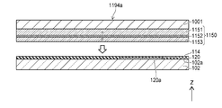
- a plurality of semiconductor growth substrates 1194 are prepared.
- the plurality of semiconductor growth substrates 1194 include a crystal growth substrate 1001, a buffer layer 1140, and a semiconductor layer 1150, respectively.
- the crystal growth substrate (first substrate) 1001 is, for example, a Si substrate, a sapphire substrate, or the like.
- the Si substrate is used as the crystal growth substrate 1001.
- a low temperature crystal growth process such as a low temperature sputtering method is used as described later, it is also possible to use a cheaper glass substrate or the like.
- the buffer layer 1140 is formed on one surface of the crystal growth substrate 1001.
- a nitride such as AlN is preferably used for the buffer layer 1140.
- the semiconductor layer 1150 is formed on the buffer layer 1140.
- the semiconductor layer 1150 includes an n-type semiconductor layer 1151, a light emitting layer 1152, and a p-type semiconductor layer 1153.
- the n-type semiconductor layer 1151, the light emitting layer 1152, and the p-type semiconductor layer 1153 are laminated in this order from the side of the buffer layer 1140.
- a vapor phase growth method (Chemical Vapor Deposition, CVD method) is used, and an organic metal vapor deposition method (Metal Organic Chemical Vapor Deposition, MOCVD method) is preferably used.
- MOCVD method Metal Organic Chemical Vapor Deposition
- the semiconductor layer 1150 can grow epitaxial crystals by a low temperature sputtering method, whereby the manufacturing cost can be reduced by using a glass substrate or an apparatus having low heat resistance. ..
- the semiconductor layer 1150 includes, for example, GaN, and more particularly includes In X Al Y Ga 1-XY N (0 ⁇ X, 0 ⁇ Y, X + Y ⁇ 1) and the like.
- crystal defects may occur due to the mismatch of crystal lattice constants, and the crystals with crystal defects exhibit n-shape. Therefore, when the semiconductor layer 1150 is formed from the n-type semiconductor layer 1151 on the crystal growth substrate 1001 as in this example, a large margin in the production process can be obtained, and the yield can be easily improved. There is an advantage.
- the support substrate 1190 is adhered to the exposed surface of the p-type semiconductor layer 1153.
- the support substrate 1190 is made of, for example, quartz glass, Si, or the like.
- the crystal growth substrate 1001 is removed to form the substrate 1195 (second substrate). For example, wet etching or laser lift-off is used to remove the crystal growth substrate 1001.
- the process up to the formation of the semiconductor growth substrate 1194 and the process of performing the processing after the substrate 1195 are formed may be executed in the same plant or may be executed in different plants.
- the substrate 1195 may be manufactured in the first plant, the substrate 1195 may be carried into a second plant different from the first plant, and the subsequent steps may be executed.
- a plurality of substrates 1195 are bonded to one substrate 102 (third substrate).
- the plurality of substrates 1195 have the semiconductor layer 1150 bonded to the first surface 102a of one substrate 102 via the buffer layer 1140.
- the surfaces of the boards are bonded to each other.
- the substrates are bonded to each other by heating and thermocompression bonding the respective substrates.
- a low melting point metal or a low melting point alloy may be used for heat crimping.
- the low melting point metal may be, for example, Sn, In, or the like, and the low melting point alloy may be, for example, an alloy containing Zn, In, Ga, Sn, Bi, or the like as a main component.
- the bonded surface of each substrate is flattened by chemical mechanical polishing (CMP), etc., and then the bonded surface is cleaned by plasma treatment in vacuum. It may be brought into close contact with each other.
- CMP chemical mechanical polishing
- the substrate 102 is, for example, a substantially rectangular glass substrate having a size of about 1500 mm ⁇ 1800 mm.
- the substrate 1195 has a rectangular shape or a square shape of several tens of mm square to 150 mm square, and has a size of, for example, about 4 inches to 6 inches in terms of wafer dimensions.
- the size of the substrate 102 is appropriately selected according to the size of the image display device and the like.
- the size of the substrate 102 is, for example, a rectangle or a square of several tens of mm square to 150 mm square
- one semiconductor layer 1150 is attached to one substrate 102 as in the case of the second embodiment described later. You may try to match.
- FIG. 6 is a perspective view illustrating the method of manufacturing the image display device of the present embodiment.
- the figure above the arrow in FIG. 6 shows that the plurality of substrates 1195 are arranged in a grid pattern.
- the figure below the arrow in FIG. 6 shows that the substrate 102 is arranged.
- the plurality of substrates 1195 arranged in a grid pattern are indicated by arrows at the positions of the alternate long and short dash lines, as will be described later. Since the quality of crystals deteriorates at and near the end of the semiconductor layer 1150, care must be taken not to form the light emitting element 150 at and near the end of the semiconductor layer 1150. As shown in FIG.
- the end portion of the semiconductor layer 1150 is formed so as to substantially coincide with the end portion of the support substrate 1190. Therefore, the plurality of substrates 1195 are arranged in a grid pattern facing the substrates 102 so as not to form a gap between the adjacent substrates 1195 as much as possible, for example, as shown by the solid line in FIG. As shown by the two-dot chain line in FIG. 6, the semiconductor layer 1150 is bonded onto the substrate 102 via the buffer layer 1140.
- the substrate 102 to which the plurality of semiconductor layers 1150 are bonded is divided before and after incorporating the color filter, and the quantity and size according to the number of divisions are divided. It can be used as an image display device. Since the end portion of the semiconductor layer 1150 having deteriorated crystal quality is preferably the end portion of the display region, the unit to be divided is preferably set to match the shape of the substrate 1195. The process of incorporating the color filter will be described later in relation to FIGS. 12 and 13A to 13D.
- FIGS. 7A to 8B are schematic cross-sectional views illustrating the manufacturing method of the image display device of the present embodiment.
- 7A-8B show two types of modifications relating to the substrate bonding process.
- the steps of FIGS. 7A to 7C can be used instead of the steps of FIGS. 5A to 5C.
- the steps of FIGS. 8A and 8B may be used.
- the semiconductor layer 1150 is formed on one surface of the crystal growth substrate 1001 without interposing the buffer layer 1140 shown in FIG. 5A.
- a plurality of semiconductor growth substrates 1194a are prepared in place of the plurality of semiconductor growth substrates 1194 shown in FIG. 5A.
- the plurality of semiconductor growth substrates 1194a include a crystal growth substrate 1001 and a semiconductor layer 1150, respectively.
- the semiconductor layer 1150 is directly formed on one surface of the crystal growth substrate 1001.
- a CVD method, a MOCVD method, or the like is used to form the semiconductor layer 1150.
- the support substrate 1190 is adhered to the exposed surface of the p-type semiconductor layer 1153.
- the crystal growth substrate 1001 is removed by wet etching, laser lift-off, or the like to form the substrate 1195a.
- the exposed surface of the n-type semiconductor layer 1151 is arranged so as to face the first surface 102a of the substrate 102. After that, the exposed surface of the n-type semiconductor layer 1151 is bonded to the first surface 102a.
- the semiconductor growth substrate 1294 is bonded to the substrate 102 without being transferred to the support substrate.
- the stacking order of the semiconductor layers formed on the crystal growth substrate 1001 is different from that in FIGS. 5A and 7A.
- the plurality of semiconductor growth substrates 1294 include a crystal growth substrate 1001 and a semiconductor layer 1150, respectively.
- the semiconductor layer 1150 is directly grown on one surface of the crystal growth substrate 1001.
- the semiconductor layer 1150 includes a p-type semiconductor layer 1153, a light emitting layer 1152, and an n-type semiconductor layer 1151.
- the p-type semiconductor layer 1153, the light emitting layer 1152, and the n-type semiconductor layer 1151 are laminated in this order from the side of the crystal growth substrate 1001.
- the semiconductor growth substrate 1294 is turned upside down, and the exposed surface of the n-type semiconductor layer 1151 is arranged so as to face the first surface 102a of the substrate 102.
- the exposed surfaces of the n-type semiconductor layers 1151 arranged to face each other are bonded to the first surface 102a of the substrate 102.
- a buffer layer is formed on the crystal growth substrate 1001, and the p-type semiconductor layer 1153, the light emitting layer 1152, and the n-type semiconductor layer 1151 are ordered from the buffer layer side on the buffer layer. It may be formed by. In this case, it is necessary to add a step of removing the residual buffer layer either before or after the step of processing the semiconductor layer 1150 to form the light emitting element.
- the method of bonding the semiconductor layer 1150 to the substrate 102 is not limited to the above, and the following method can also be used. That is, the semiconductor layer 1150 is housed in a container in a state where the crystal growth substrate 1001 is removed after being formed on the crystal growth substrate 1001, and the support substrate 1190 is mounted and stored in the container, for example. After storage, the semiconductor layer 1150 is taken out of the container and bonded to the substrate 102. Further, the semiconductor layer 1150 is stored in a container without being mounted on the support substrate 1190. After storage, the semiconductor layer 1150 is taken out of the container and bonded to the substrate 102 as it is.
- FIGS. 9A to 10B are schematic cross-sectional views illustrating the manufacturing method of the image display device of the present embodiment. As shown in FIG. 9A, the support substrate 1190 shown in FIG. 5C is removed by wet etching, laser lift-off, or the like.
- a plurality of substrates 1195 are arranged adjacent to each other and bonded to the substrate 102.
- the position X1 is a position where the respective ends of the substrates 1195 adjacent to each other are arranged. At position X1, the ends of the semiconductor layer 1150 are also adjacent to and close to each other.
- the semiconductor layer 1150 shown in FIG. 9A is processed into a desired shape by etching to form a light emitting element 150.
- the light emitting element 150 is formed at a position sufficiently distant from the region including the position X1.
- the region including the position X1 is determined based on the evaluation result by evaluating the crystal quality near the end of the semiconductor layer 1150.
- connection portion 151a is formed, and then another portion is formed by further etching.
- a dry etching process is used for forming the light emitting element 150, and anisotropic plasma etching (Reactive Ion Etching, RIE) is preferably used.
- RIE reactive Ion Etching
- the buffer layer 1140 shown in FIG. 9A is etched together with the semiconductor layer 1150 and remains as the buffer layer 140 between the first surface 102a and the n-type semiconductor layer 151.
- a first interlayer insulating film 156 (first insulating film) that covers the first surface 102a, the buffer layer 140, and the light emitting element 150 is formed.
- the TFT lower layer film 106 is formed on the first interlayer insulating film 156 by, for example, CVD.
- the TFT channel 104 is formed at a predetermined position on the TFT underlayer film 106.
- the transistor 103 is formed as follows. First, amorphous Si is formed into the shape of the TFT channel 104. For example, CVD or the like is used for forming an amorphous Si film. The formed amorphous Si film is polycrystallized by laser annealing to form a TFT channel 104.
- the source electrode and the drain electrode of the TFT channel 104 are formed by introducing impurity ions such as B + into the regions 104s and 104d by using, for example, an ion implantation technique.
- the step of forming the source electrode and the drain electrode may be performed after the step of forming the gate 107.
- the insulating layer 105 is formed over the TFT underlayer film 106 and the TFT channel 104.
- the insulating layer 105 is formed by, for example, CVD or the like.
- the gate 107 is formed at a position on the TFT channel 104 via the insulating layer 105.
- An appropriate forming method is used for forming the gate 107 depending on the material of the gate 107. For example, when the gate 107 is polycrystalline Si, it is formed by laser annealing amorphous Si to polycrystalline Si, similarly to the TFT channel 104.
- the second interlayer insulating film 108 (second insulating film) is provided so as to cover the insulating layer 105 and the gate 107.
- An appropriate manufacturing method is applied to the formation of the second interlayer insulating film 108 depending on the material of the second interlayer insulating film 108. For example, when the second interlayer insulating film 108 is formed of SiO 2 , techniques such as ALD and CVD are used.
- the flatness of the second interlayer insulating film 108 may be such that the wiring layer 110 can be formed, and the flattening step does not necessarily have to be performed.
- the number of steps can be reduced. For example, when there is a portion around the light emitting element 150 where the thickness of the second interlayer insulating film 108 becomes thin, the depth of the via hole 162k becomes shallow, so that a sufficient opening diameter can be secured. Therefore, it becomes easy to secure the electrical connection by the via, and it is possible to suppress the decrease in the yield due to the poor electrical characteristics.
- the via hole 162k is formed so as to penetrate the second interlayer insulating film 108, the insulating layer 105, the TFT lower layer film 106, and the first interlayer insulating film 156 and reach the surface of the connecting portion 151a.
- the opening 158 reaches the light emitting surface 153S by removing a part of the second interlayer insulating film 108, a part of the insulating layer 105, a part of the TFT lower layer film 106, and a part of the first interlayer insulating film 156. Is formed in.
- a part of the second interlayer insulating film 108, a part of the insulating layer 105, a part of the TFT lower layer film 106, and a part of the first interlayer insulating film 156 are placed on the light emitting surface 153S of these insulating layers and insulating films. It is the formed part.
- the via hole 112d is formed so as to penetrate the second interlayer insulating film 108 and the insulating layer 105 and reach the surface of the region 104d.
- the via hole 112s is formed so as to penetrate the second interlayer insulating film 108 and the insulating layer 105 and expose the surface of the region 104s.
- RIE is used for forming via holes and openings.
- the via 161k is formed by filling the via hole 162k shown in FIG. 10A with a conductive material.
- the vias 111d and 111s are also formed by filling the via holes 112d and 112s shown in FIG. 10A with a conductive material, respectively.
- the wiring layer 110 is formed on the second interlayer insulating film 108, and the wirings 110k, 110d, 110s are formed.
- the wiring layer 110 may be formed at the same time as the vias 161k, 111d, 111s are formed.
- 11A and 11B are schematic cross-sectional views illustrating a method of manufacturing a modified example of the image display device of the present embodiment.
- 11A and 11B show a process for forming the subpixel 20a shown in FIG.
- the same steps as described above are obtained until the second interlayer insulating film 108 is formed and the via holes 162k, 112d, 112s are formed.
- the steps of FIGS. 11A and 11B will be described as being executed after the step of FIG. 10A.
- the vias 161k, 111d, 111s are formed by filling the via holes 162k, 112d, 112s shown in FIG. 10A with a conductive material.
- the wiring layer 110 is formed, and the wirings 110k, 110d1, 110s are formed.
- one end of the wiring 110d1 is connected to the via 111d.
- the other end of the wiring 110d1 is not directly connected to the light emitting surface 153S and is located away from the opening 158.
- the vias 161k, 111d, 111s and the wiring layer 110 may be formed at the same time as in the case of the first embodiment.
- a translucent electrode 159d is formed on the wiring 110d1 and on the light emitting surface 153S.
- the translucent electrode 159d is also formed between the wiring 110d1 and the light emitting surface 153S, and electrically connects the wiring 110d1 and the light emitting surface 153S.
- the translucent electrode 159s is formed over the wiring 110s.
- the translucent electrodes 159d and 159s are formed at the same time.
- the roughening treatment on the light emitting surface 153S can be performed at an arbitrary timing from the provision of the opening 158 to the formation of the translucent electrode 159d.
- the sub-pixel 20a of the modified example is formed.
- the circuit of FIG. 3 is a drive circuit that drives the light emitting element 150 by the selection transistor 24, the drive transistor 26, and the capacitor 28.
- a drive circuit is formed in the sub-pixels 20 and 20a.
- a part of the circuit other than the drive circuit is formed on the peripheral portion of the display area 2 shown in FIG. 1, for example, outside the subpixels 20 and 20a.
- the row selection circuit 5 shown in FIG. 3 is formed at the same time as a drive transistor, a selection transistor, and the like, and is formed on the peripheral edge of the display region 2. That is, the row selection circuit 5 can be incorporated at the same time by the above-mentioned manufacturing process.
- the signal voltage output circuit 7 be incorporated in a semiconductor device manufactured by a manufacturing process capable of high integration by microfabrication.
- the signal voltage output circuit 7 is mounted on another board together with the CPU and other circuit elements, and is provided, for example, before the incorporation of the color filter described later, or after the incorporation of the color filter, for example, at the peripheral edge of the display area. It is interconnected with the sub-pixels 20 and 20a via a connector or the like.
- each light emitting element 150 can form an image in the display area 2 by radiating light upward from the light emitting surface 153S.
- the light emitting efficiency is substantially lowered because the substrate 102 has translucency. Therefore, for example, by providing a light reflecting film, a light reflecting plate, or the like on the side of the surface of the substrate 102 facing the first surface 102a, light scattering in the direction of the substrate 102 is reflected in the direction of the light emitting surface 153S. Can be done.
- a light reflecting film or the like may be provided on the substrate 102, or may be provided inside a case, a frame, or the like for fixing the image display device 1.
- FIG. 12 is a schematic cross-sectional view illustrating the method for manufacturing the image display device of the present embodiment.
- the figure above the arrow shows the configuration including the color filter 180
- the figure below the arrow shows the structure including the light emitting element 150 and the like formed in the above-mentioned steps.
- FIG. 12 shows a step of adhering a color filter to a structure including a light emitting element 150 and the like by an arrow.
- the components other than the components on the illustrated substrate 102 are omitted from the display.
- the omitted components are the buffer layer 140 shown in FIG. 1, the circuit 101 including the TFT channel 104, the wiring layer 110, and the like, and the via 161k. Further, in FIG.
- a part of the color conversion member such as the color filter 180 is displayed.
- the light emitting element 150, the first interlayer insulating film 156, the circuit 101, the TFT lower layer film 106 and the surface resin layer 170 are referred to as a light emitting circuit unit 172, and the substrate 102, the light emitting circuit unit 172 and the like.
- a structure including components whose display is omitted is referred to as a structure 1192. Note that, in FIG. 12, among the elements constituting the circuit 101, the display of the TFT channel 104, the vias 111s, 111d, and the wiring layer 110 is omitted.
- the color filter (wavelength conversion member) 180 is adhered to the structure 1192 on one side.
- the other surface of the color filter 180 is adhered to the glass substrate 186.
- a transparent thin film adhesive layer 188 is provided on one surface of the color filter 180, and is adhered to the exposed surface of the surface resin layer 170 of the structure 1192 via the transparent thin film adhesive layer 188.
- the color filter 180 has color conversion units arranged in the positive direction of the X-axis in the order of red, green, and blue.
- a red color conversion layer 183R is provided on the first layer
- a green color conversion layer 183G is provided on the first layer
- a filter layer 184 is provided on the second layer in each case.
- Each is provided.
- a single-layer color conversion layer 183B may be provided, or a filter layer 184 may be provided.
- a light-shielding unit 181 is provided between the color conversion units, it goes without saying that the frequency characteristics of the filter layer 184 can be changed for each color of the color conversion unit.
- the color filter 180 is attached to the structure 1192 by aligning the positions of the color conversion layers 183R, 183G, and 183B of each color with the positions of the light emitting element 150.
- 13A to 13D are schematic cross-sectional views showing a modified example of the manufacturing method of the image display device of the present embodiment.
- 13A to 13D show a method of forming a color filter by an inkjet method.
- a structure 1192 in which components such as a light emitting element 150 are formed on a substrate 102 is prepared.
- a light-shielding portion 181 is formed on the structure 1192.
- the light-shielding portion 181 is formed by using, for example, screen printing, photolithography technology, or the like.
- the phosphor corresponding to the emission color is ejected from the inkjet nozzle to form the color conversion layer 183.
- the phosphor colors the region where the light-shielding portion 181 is not formed.
- the fluorescent material for example, a general fluorescent material, a perovskite fluorescent material, or a fluorescent paint using a quantum dot fluorescent material is used.
- a perovskite phosphor material or a quantum dot phosphor material it is preferable because each emission color can be realized, the monochromaticity is high, and the color reproducibility can be high.
- a drying process is performed at an appropriate temperature and time. The thickness of the coating film at the time of coloring is set to be thinner than the thickness of the light-shielding portion 181.
- the color conversion layer 183 is not formed for the subpixels that emit blue light if the color conversion unit is not formed. Further, when the blue color conversion layer is formed for the subpixels of blue light emission, if the color conversion unit may be one layer, the thickness of the coating film of the blue phosphor is preferably the light-shielding portion 181. It is said to be about the same as the thickness of.
- the paint for the filter layer 184 is ejected from the inkjet nozzle.
- the paint is applied over the coating film of the phosphor.
- the total thickness of the paint film of the phosphor and the paint is about the same as the thickness of the light-shielding portion 181.
- the color conversion layer 183 be as thick as possible in order to improve the color conversion efficiency.
- the color conversion layer 183 is too thick, the emitted light of the color-converted light is approximated to Lambersian, whereas the emission angle of the non-color-converted blue light is limited by the light-shielding portion 181. .. Therefore, there arises a problem that the display color of the display image is dependent on the viewing angle.
- the thickness of the color conversion layer 183 should be about half the opening size of the light-shielding portion 181. Is desirable.
- the pitch of the subpixels 20 is about 30 ⁇ m, so that the thickness of the color conversion layer 183 is preferably about 15 ⁇ m.
- the color conversion material is made of spherical phosphor particles, it is preferable to stack them in a close-packed structure in order to suppress light leakage from the light emitting element 150. For that purpose, at least three layers of particles need to be formed. Therefore, the particle size of the phosphor material constituting the color conversion layer 183 is preferably, for example, about 5 ⁇ m or less, and more preferably about 3 ⁇ m or less.
- FIG. 14 is a schematic perspective view illustrating the image display device according to the present embodiment.
- a light emitting circuit unit 172 having a large number of subpixels 20 is provided on the substrate 102.
- a color filter 180 is provided on the light emitting circuit unit 172.
- Other embodiments and modifications described later have the same configuration as shown in FIG.
- the semiconductor layer 1150 is bonded to the substrate 102, and then the semiconductor layer 1150 is etched to form the light emitting element 150. After that, the light emitting element 150 is covered with the first interlayer insulating film 156, and a circuit 101 including a circuit element such as a transistor 103 for driving the light emitting element 150 is built on the first interlayer insulating film 156. Therefore, the manufacturing process is remarkably shortened as compared with transferring the individualized light emitting elements to the substrate 102 individually.
- the manufacturing method of the image display device of the present embodiment is as follows. The effect is obtained.
- the light emitting element is formed by etching after the entire semiconductor layer 1150 is bonded to the substrate 102, so that the transfer step is completed in one time. Therefore, in the manufacturing method of the image display device 1 of the present embodiment, the time of the transfer step can be shortened and the number of steps can be reduced as compared with the conventional manufacturing method.
- the semiconductor layer 1150 is bonded to the substrate 102 at the wafer level without being fragmented in advance or forming an electrode at a position corresponding to the circuit element. Therefore, alignment at the bonding stage is not required. Therefore, the bonding process can be easily performed in a short time. Since it is not necessary to align the light emitting element 150 at the time of bonding, it is easy to reduce the size of the light emitting element 150, which is suitable for a high-definition display.
- the glass substrate formed as described above is covered with an interlayer insulating film, and a drive circuit including a TFT or the like, a scanning circuit, or the like is formed on the flattened surface by using an LTPS process or the like. Can be done. Therefore, there is an advantage that the existing flat panel display manufacturing process and plant can be used.
- the light emitting element 150 formed in the lower layer than the transistor 103 or the like forms a via penetrating the first interlayer insulating film 156, the TFT lower layer film 106, the insulating layer 105, and the second interlayer insulating film 108.
- This makes it possible to electrically connect to a power supply line, a ground line, a driving transistor, or the like formed on the upper layer.
- a uniform connection structure can be easily realized and the yield can be improved. Therefore, the decrease in yield due to poor connection of the light emitting element or the like is suppressed.
- FIG. 15 is a schematic cross-sectional view illustrating a part of the image display device according to the present embodiment.
- the present embodiment is described above in that the light reflecting layer 120 including the light reflecting plate 120a is provided on the first surface 102a, and the light emitting element 250 is provided on the light reflecting plate 120a via the insulating layer 114.
- the n-type semiconductor layer 251 provides a light emitting surface 251S.
- This embodiment differs from the other embodiments described above in that it has a configuration in which the light emitting element 250 is driven by the transistor 203.
- the same components as in the case of other embodiments are designated by the same reference numerals, and detailed description thereof will be omitted as appropriate.
- the subpixel 220 of the image display device of the present embodiment includes a substrate 102, a light reflecting layer 120, a light emitting element 250, a first interlayer insulating film 156, a transistor 203, and a second interlayer. It includes an insulating film 108, a via 261a, and a wiring layer 110.
- the light reflecting layer 120 (layer having light reflecting property) is provided on the first surface 102a.
- the light reflecting layer 120 includes a light reflecting plate 120a.
- the light reflection plate 120a (first portion) is a film-like, layer-like, or plate-like member having a shape such as a square or an arbitrary polygon, an ellipse, or a circle in an XY plan view.
- the light reflection layer 120 includes a plurality of light reflection plates 120a, and the light reflection plate 120a is provided at each location where the light emitting element 250 is provided. In this example, the plurality of light reflection plates 120a are separated from each other.
- the outer circumference of the light reflecting plate 120a may be set to include the outer circumference of the light emitting element 250 when the light emitting element 250 is projected in the XY plan view.
- the light reflection plate 120a may be provided for each light emitting element 250, or may be provided for each of a plurality of light emitting elements 250.
- the light reflection plate 120a is not separated for each light emitting element 250, and may be formed by being connected in a grid pattern, for example. In that case, the light emitting element 250 is provided, for example, on the position of the grid where the light reflection plates 120a intersect.
- the light reflecting layer 120 may be a single light reflecting plate 120a.
- the single light reflection plate 120a is provided on the entire surface of the display area 2 shown in FIG. 2, for example.
- the light reflecting plate 120a is made of a material having light reflecting property.
- the light reflection plate 120a is made of a metal material such as Ag or an alloy containing Ag. Any material having light reflectivity can be used, not limited to Ag or the like.
- An insulating layer 114 is provided over the first surface 102a, the light reflecting layer 120, and the light reflecting plate 120a.
- the insulating layer 114 is formed of an oxide film such as SiO 2 or the like.
- the insulating layer 114 is provided to insulate the light reflecting plate 120a from the light emitting element 250. Further, as will be described later, the insulating layer 114 provides a flat surface when the substrates are bonded.
- the light emitting element 250 is provided on the light reflecting plate 120a via the insulating layer 114.
- the light emitting element 250 is provided directly above the light reflecting plate 120a.
- the outer circumference of the light reflection plate 120a is set so as not to include the outer circumference of the transistor 203 when the transistor 203 is projected onto the plane including the light reflection plate 120a in XY plan view.
- the transistor 203 is less likely to receive the reflected light from the light reflecting plate 120a, and the probability of causing a malfunction can be sufficiently reduced.
- the outer circumference of the transistor 203 in the XY plane view is the outer circumference of the TFT channel in the XY plane view.
- the light emitting element 250 includes a light emitting surface 251S.
- the light emitting element 250 is a prismatic or columnar element having a bottom surface 253B on the first surface 102a, as in the case of the other embodiments described above.
- the light emitting surface 251S is a surface facing the bottom surface 253B.
- the bottom surface 253B is, in this example, a surface in contact with the insulating layer 114.
- the light emitting element 250 includes a p-type semiconductor layer 253, a light emitting layer 252, and an n-type semiconductor layer 251.
- the p-type semiconductor layer 253, the light emitting layer 252, and the n-type semiconductor layer 251 are laminated in this order from the bottom surface 253B toward the light emitting surface 251S.
- the light emitting surface 251S is provided by the n-type semiconductor layer 251. Since the n-type semiconductor layer 251 can have a lower resistance value than the p-type semiconductor layer 253, the thickness can be increased. Therefore, roughening of the light emitting surface 251S becomes easy.
- the light emitting element 250 includes a connection portion 253a.
- the connection portion 253a is provided on the insulating layer 114 so as to project in one direction from the p-type semiconductor layer 253.
- the height of the connecting portion 253a is the same as that of the p-type semiconductor layer 253 or lower than that of the p-type semiconductor layer 253, and the light emitting element 250 is formed in a stepped shape.
- the connection portion 253a is p-type and is electrically connected to the p-type semiconductor layer 253.
- the connection portion 253a is connected to one end of the via 261a and electrically connects the p-type semiconductor layer 253 to the via 261a.
- the light emitting element 250 has the same XY plan view shape as the light emitting element 150 of the other embodiment described above. An appropriate shape is selected according to the layout of the circuit element and the like.
- the shape of the light reflection plate 120a in the XY plane view can be any shape as described above, and an appropriate shape is selected according to the layout of the circuit element or the like.
- the light emitting element 250 is a light emitting diode similar to the light emitting element 150 of the other embodiment described above. That is, the wavelength of the light emitted by the light emitting element 250 is, for example, blue light emission of about 467 nm ⁇ 20 nm or blue-purple light emission of about 410 nm ⁇ 20 nm.
- the wavelength of the light emitted by the light emitting element 250 is not limited to the above-mentioned value, and may be appropriate.
- the transistor 203 is provided on the TFT lower layer film 106.
- the transistor 203 is an n-channel TFT.
- the transistor 203 includes a TFT channel 204 and a gate 107.
- the transistor 203 is formed by an LTPS process or the like, as in the other embodiments described above.
- the circuit 101 includes a TFT channel 204, an insulating layer 105, a second interlayer insulating film 108, vias 111s, 111d, and a wiring layer 110.
- the TFT channel 204 includes regions 204s, 204i, 204d.
- the regions 204s, 204i, 204d are provided on the TFT underlayer film 106.
- the regions 204s and 204d are doped with n-type impurities such as phosphorus ions (P ⁇ ).
- the region 204s is ohmic contacted with the via 111s.
- the area 204d is ohmic contacted with the via 111d.
- the gate 107 is provided on the TFT channel 204 via the insulating layer 105.
- the insulating layer 105 insulates the TFT channel 204 from the gate 107.
- the transistor 203 when a voltage higher than the region 204s is applied to the gate 107, a channel is formed in the region 204i.
- the current flowing between the regions 204s and 204d is controlled by the voltage of the gate 107 with respect to the region 204s.
- the TFT channel 204 and the gate 107 are formed of the same material and manufacturing method as the TFT channel 104 and the gate 107 in the case of the above-mentioned other embodiments.
- the wiring layer 110 includes wirings 110s, 110d1, and 210a.
- the wirings 110s and 110d1 are the same as in the modified example of the first embodiment described above in FIG.
- a part of the wiring 210a (first wiring) is provided above the connection portion 253a.
- the other portion of the wiring 210a extends to, for example, the power supply line 3 shown in FIG. 16 described later, and is connected to the power supply line 3.
- the vias 111s and 111d are provided so as to penetrate the second interlayer insulating film 108.
- the via 111s is provided between the wiring 110s and the area 204s.
- the via 111s electrically connects the wiring 110s and the area 204s.
- the via 111d is provided between the wiring 110d1 and the area 204d.
- the via 111d electrically connects the wiring 110d1 and the area 204d.
- the vias 111s and 111d are formed of the same materials and manufacturing methods as in the other embodiments described above.
- the via 261a is provided so as to penetrate the second interlayer insulating film 108, the insulating layer 105, the TFT lower layer film 106, and the first interlayer insulating film 156.
- the via 261a is provided between the wiring 210a and the connecting portion 253a, and electrically connects the wiring 210a and the connecting portion 253a.
- the wiring 110s (second wiring) is electrically connected to, for example, the ground wire 4 shown in FIG. 16 described later.
- the wiring 110d1 is electrically connected to the n-type semiconductor layer 251 via the translucent electrode 159d.
- the translucent electrode 159d is provided over the light emitting surface 251S of the roughened n-type semiconductor layer 251.
- the translucent electrode 159d is provided over the wiring 110d1.
- the translucent electrode 159d is also provided between the light emitting surface 251S and the wiring 110d, and electrically connects the n-type semiconductor layer 251 and the wiring 110d.
- the wiring 110d may be extended and directly connected to the n-type semiconductor layer 251 as in the example shown in FIG.
- FIG. 16 is a schematic block diagram illustrating an image display device according to the present embodiment.
- the image display device 201 of the present embodiment includes a display area 2, a row selection circuit 205, and a signal voltage output circuit 207.
- the sub-pixels 220 are arranged in a grid pattern on the XY plane, as in the case of the other embodiments described above.
- Pixel 10 includes a plurality of sub-pixels 220 that emit light of different colors, as in the case of the other embodiments described above.
- the subpixel 220R emits red light.
- the subpixel 220G emits green light.
- the subpixel 220B emits blue light.
- the emission color and brightness of one pixel 10 are determined by the three types of sub-pixels 220R, 220G, and 220B emitting light at a desired brightness.
- One pixel 10 includes three sub-pixels 220R, 220G, 220B, and the sub-pixels 220R, 220G, 220B are linearly arranged on the X-axis, for example, as in this example.
- sub-pixels of the same color may be arranged in the same column, or sub-pixels of different colors may be arranged in each column as in this example.
- the subpixel 220 includes a light emitting element 222, a selection transistor 224, a drive transistor 226, and a capacitor 228.
- the selection transistor 224 may be displayed as T1
- the drive transistor 226 may be displayed as T2
- the capacitor 228 may be displayed as Cm.
- the light emitting element 222 is provided on the power supply line 3 side, and the drive transistor 226 connected in series with the light emitting element 222 is provided on the ground line 4 side. That is, the drive transistor 226 is connected to the lower potential side than the light emitting element 222.
- the drive transistor 226 is an n-channel transistor.
- a selection transistor 224 is connected between the gate electrode of the drive transistor 226 and the signal line 208.
- the capacitor 228 is connected between the gate electrode of the drive transistor 226 and the ground wire 4.
- the row selection circuit 205 and the signal voltage output circuit 207 supply a signal voltage having a polarity different from that of the above-mentioned other embodiments to the signal line 208 in order to drive the drive transistor 226 which is an n-channel transistor.
- the row selection circuit 205 supplies a selection signal to the scanning line 206 so as to sequentially select one row from the array of subpixels 220 in the m row.
- the signal voltage output circuit 207 supplies a signal voltage having the required analog voltage value for each subpixel 220 in the selected row.
- the drive transistor 226 of the subpixel 220 in the selected row causes a current corresponding to the signal voltage to flow through the light emitting element 222.
- the light emitting element 222 emits light with a brightness corresponding to the flowing current.
- FIG. 17A to 19B are schematic cross-sectional views illustrating the method of manufacturing the image display device of the present embodiment.
- one semiconductor growth substrate (second substrate) 1194a is prepared and bonded to one substrate 102 (third substrate).
- a plurality of semiconductor growth substrates can be prepared and bonded to one substrate 102.
- the above-mentioned other embodiments and various modifications thereof can be applied.
- the semiconductor growth substrate 1194a has a semiconductor layer 1150 formed on the crystal growth substrate (first substrate) 1001.
- the crystal growth substrate 1001 is, for example, a Si substrate, a sapphire substrate, or the like, and is preferably a Si substrate.
- a cheaper glass substrate can also be used.
- the semiconductor layer 1150 includes an n-type semiconductor layer 1151, a light emitting layer 1152, and a p-type semiconductor layer 1153.
- the n-type semiconductor layer 1151, the light emitting layer 1152, and the p-type semiconductor layer 1153 are laminated in the order of the n-type semiconductor layer 1151, the light emitting layer 1152, and the p-type semiconductor layer 1153 from the side of the crystal growth substrate 1001.
- the formation of the semiconductor layer 1150 is the same as in the case of the other embodiments described above, and by performing epitaxial growth by a CVD method, a MOCVD method, or a low temperature sputtering method, a low temperature process of 700 ° C. or lower can be achieved.
- the light reflecting layer 120 (layer having light reflecting property) is formed on the first surface 102a before the semiconductor layer 1150 is bonded to the substrate 102.
- the light reflecting layer 120 may be formed by sputtering or the like, or may be formed by applying Ag paste or the like to the shape of the light reflecting plate 120a and then firing the light reflecting layer 120.
- the light reflection plate 120a of the light reflection layer 120 is provided at a position where the light emitting element 250 is formed.
- the insulating layer 114 is formed over the first surface 102a, the light reflecting layer 120, and the light reflecting plate 120a before the semiconductor layer 1150 is attached to the substrate 102.
- the insulating layer 114 is formed by CVD or the like. Since the exposed surface of the insulating layer 114 is a surface to be bonded to the substrate 102, it is flattened by CMP or the like.
- the semiconductor growth substrate 1194a is arranged so that the exposed surface of the p-type semiconductor layer 1153 faces the flattened exposed surface of the insulating layer 114 provided on the substrate 102.
- the exposed surface of the p-type semiconductor layer 1153 is bonded to the exposed surface of the insulating layer 114.
- the crystal growth substrate 1001 shown in FIG. 17A is removed by wet etching, laser lift-off, or the like.
- the semiconductor layer 1150 shown in FIG. 17B is formed into a desired shape by etching to form a light emitting element 250.
- the light emitting element 250 is formed with the remaining portion after forming the connection portion 253a.
- a dry etching process is used, and RIE is preferably used.
- the first interlayer insulating film 156 is formed so as to cover the insulating layer 114 and the light emitting element 250.
- the TFT lower layer film 106 is formed by CVD or the like over the first interlayer insulating film 156.
- the TFT channel 204 is formed on the flattened TFT underlayer film 106.
- An insulating layer 105 covering the TFT underlayer film 106 and the TFT channel 204 is formed.
- a gate 107 is formed on the TFT channel 204 via the insulating layer 105.
- a second interlayer insulating film 108 is formed so as to cover the insulating layer 105 and the gate 107.
- the via hole 162a is formed so as to penetrate the second interlayer insulating film 108, the insulating layer 105, the TFT lower layer film 106, and the first interlayer insulating film 156 and reach the surface of the connecting portion 253a.
- the opening 158 reaches the light emitting surface 251S by removing a part of the second interlayer insulating film 108, a part of the insulating layer 105, a part of the TFT lower layer film 106, and a part of the first interlayer insulating film 156. Is formed in.
- a part of the second interlayer insulating film 108, a part of the insulating layer 105, a part of the TFT lower layer film 106, and a part of the first interlayer insulating film 156 are placed on the light emitting surface 251S of these insulating layers and insulating films. It is the formed part.
- the via hole 112d is formed so as to penetrate the second interlayer insulating film 108 and the insulating layer 105 and reach the surface of the region 204d.
- the via hole 112s is formed so as to penetrate the second interlayer insulating film 108 and the insulating layer 105 and reach the surface of the region 204s.
- RIE is used for forming via holes and openings.
- the via 261a is formed by filling the via hole 162a shown in FIG. 19A with a conductive material.
- the vias 111d and 111s are also formed by filling the via holes 112d and 112s shown in FIG. 19A with a conductive material, respectively.
- the wiring layer 110 is formed, and the wirings 210a, 110d1, 110s are formed.
- the wiring layer 110 may be formed at the same time as the vias 261a, 111d1, 111s are formed.
- a translucent conductive film that covers the second interlayer insulating film 108, the light emitting surface 251S, and the wiring layer 110 is formed. Photolithography forms the desired translucent electrodes 159d, 159s.
- a translucent electrode 159d is formed on the light emitting surface 251S and over the wiring 110d1.
- the translucent electrode 159d is also formed between the light emitting surface 251S and the wiring 110d, and electrically connects the light emitting surface 251S and the wiring 110d.
- the translucent electrode 159s is formed over the wiring 110s.
- the translucent electrodes 159d and 159s are formed at the same time.
- a translucent electrode may be formed on the wiring 210a.
- the sub-pixel 220 of the image display device 201 of the present embodiment is formed by providing a color filter 180 (wavelength conversion member) or the like.
- the effect of the image display device of this embodiment will be described.
- the time of the transfer step for forming the light emitting element 250 can be shortened and the number of steps can be reduced.
- the n-type semiconductor layer 251 as the light emitting surface 251S, the light emitting surface 251S can be sufficiently roughened. Therefore, the luminous efficiency is improved, and the increase in loss due to contact resistance can be suppressed.
- FIG. 20 is a schematic cross-sectional view illustrating a part of the image display device according to the present embodiment.
- This embodiment differs from the other embodiments described above in that the light emitting element 250 having the n-type semiconductor layer 251 as the light emitting surface 251S is driven by the p-type transistor 103.
- the same components as in the case of the other embodiments described above are designated by the same reference numerals, and detailed description thereof will be omitted as appropriate.
- the subpixel 320 of the image display device of the present embodiment includes a substrate 102, a light emitting element 250, a first interlayer insulating film 156, a transistor 103, a second interlayer insulating film 108, and vias. 361a and a wiring layer 110 are included.
- the transistor 103 is a p-channel TFT.
- the light emitting element 250 provides a light emitting surface 251S with an n-type semiconductor layer 251.
- the light emitting element 250 is provided on the light reflecting plate 120a via the insulating layer 114.
- the light reflection plate 120a is provided with the same configuration as in the case of the other embodiments described above.
- the light reflection plate 120a is provided directly below the light emitting element 250.
- the outer periphery of the light reflecting plate 120a is set to include the outer periphery of the light emitting element 250 when the light emitting element 250 is projected in XY plan view.
- the light reflecting plate 120a reflects the light scattered downward of the light emitting element 250 toward the light emitting surface 251S side, and substantially improves the light emitting efficiency.
- the light emitting element 250 is a prismatic or columnar element having a bottom surface 253B on the first surface 102a.
- the light emitting surface 251S is a surface facing the bottom surface 253B.
- the bottom surface 253B is, in this example, a surface in contact with the insulating layer 114.
- the light emitting element 250 includes a p-type semiconductor layer 253, a light emitting layer 252, and an n-type semiconductor layer 251.
- the p-type semiconductor layer 253, the light emitting layer 252, and the n-type semiconductor layer 251 are laminated in this order from the bottom surface 253B toward the light emitting surface 251S.
- the p-type semiconductor layer 253 includes a connection portion 253a.
- the connecting portion 253a is provided so as to project on the insulating layer 114 in one direction from the p-type semiconductor layer 253.
- the connection portion 253a is connected to one end of the via 361a, and electrically connects the p-type semiconductor layer 253 to the via 361a.
- the configuration of the transistor 103 is the same as that of the first embodiment.
- the detailed configuration of the transistor 103 will be omitted.
- the wiring layer 110 is formed on the second interlayer insulating film 108.
- the wiring layer 110 includes wirings 310k, 310a, 110d1, 110s.
- the wiring 310a and the wiring 310k are provided above the light emitting element 250 and in close proximity to the light emitting element 250.
- the wiring 310a (third wiring) is provided above the connection portion 253a.
- the wiring 310k (fourth wiring) is provided at a position that does not intersect with the wiring 310a.
- the via 361a is provided so as to penetrate the second interlayer insulating film 108, the insulating layer 105, the TFT lower layer film 106, and the first interlayer insulating film 156.
- the via 361a is provided between the wiring 310a and the connection portion 253a.
- the via 361a electrically connects the wiring 310a and the connecting portion 253a.
- Vias 111d and 111s are provided in the same manner as in the case of the other embodiments described above.
- the translucent electrode 359k is provided over the wiring 310k.
- the translucent electrode 359k is provided over the light emitting surface 251S.
- the translucent electrode 359k is also provided between the wiring 310k and the light emitting surface 251S, and electrically connects the wiring 310k and the light emitting surface 251S.
- the wiring 310k and the translucent electrode 359k are connected to, for example, the ground wire 4 shown in FIG. Therefore, the n-type semiconductor layer 251 is electrically connected to the ground wire 4 via the light emitting surface 251S, the translucent electrode 359k, and the wiring 310k.
- a translucent electrode 359d is provided over the wiring 310a.
- a translucent electrode 359d is provided over the wiring 110d1.
- the translucent electrode 359k is also provided between the wiring 310a and the wiring 110d1, and electrically connects the wiring 310a and the wiring 110d1. Therefore, the p-type semiconductor layer 253 is electrically connected to the region 104d via the connection portion 253a, the via 361a, the wiring 310a, the translucent electrode 359d, the wiring 110d1, and the via 111d.
- the translucent electrode 159s is provided over the wiring 110s.
- the wiring 110s and the translucent electrode 159s are connected to, for example, the power line 3 shown in FIG. Therefore, the region 104s of the transistor 103 is electrically connected to the power supply line 3 via the via 111s, the wiring 110s, and the translucent electrode 159s.
- the vias 361a, 111d, 111s and the wirings 310k, 310a, 110d1, 110s are formed of the same materials and manufacturing methods as in the case of the other embodiments and modifications thereof described above.
- a color filter 180 and the like are further provided.
- 21A to 22B are schematic cross-sectional views illustrating the manufacturing method of the image display device of the present embodiment.
- the process can be the same as that of the second embodiment until the semiconductor layer 1150 formed on the crystal growth substrate 1001 is bonded to the substrate 102 on which the light reflecting layer 120 and the insulating layer 114 are formed. ..
- the method of bonding the substrates described in the first embodiment may be used.
- the steps of FIGS. 21A to 22B will be described as being executed in the steps after FIG. 17B.
- the semiconductor layer 1150 shown in FIG. 17B is processed into a desired shape to form a light emitting element 250.
- the light emitting element 250 is formed with other portions.
- the first interlayer insulating film 156 covering the insulating layer 114 and the light emitting element 250 is formed.
- the TFT underlayer film 106 is formed, the TFT channel 104 is formed, the insulating layer 105 is formed, and the gate 107 is formed.
- a second interlayer insulating film 108 that covers the insulating layer 105 and the gate 107 is formed.
- the via hole 362a is formed so as to penetrate the second interlayer insulating film 108, the insulating layer 105, the TFT lower layer film 106, and the first interlayer insulating film 156 and reach the surface of the connecting portion 253a.
- the openings 158 and the via holes 112d, 112s are formed in the same manner as in the other embodiments described above.
- the via holes 362a, 112d, 112s shown in FIG. 22A are filled with a conductive material to form vias 361a, 111d, 111s.
- the wiring layer 110 is formed on the second interlayer insulating film 108.
- a translucent conductive film is formed on the wiring layer 110, and translucent electrodes 359k, 359d, and 159s are formed.
- the image display device of the present embodiment it is possible to have a circuit configuration in which the light emitting element 250 is driven by the p-channel transistor 103 while the n-type semiconductor layer 251 is used as the light emitting surface 251S.
- This has the effect of facilitating roughening of the light emitting surface, as in the second embodiment. Further, by roughening the light emitting surface, the luminous efficiency is improved and the effect of suppressing the increase in loss due to contact resistance can be obtained.
- FIG. 23 is a schematic cross-sectional view illustrating a part of the image display device according to the present embodiment.
- the image display device of the present embodiment includes a flexible substrate 402 instead of the glass substrate.
- Circuit elements such as light emitting elements and transistors are formed on the first surface 402a of the substrate 402.
- the same components are designated by the same reference numerals, and detailed description thereof will be omitted as appropriate.
- the image display device of the present embodiment includes subpixels 420.
- the subpixel 420 includes the substrate 402.
- the substrate 402 includes a first surface 402a.
- a layer 113 containing a silicon compound is formed on the first surface 402a.
- the layer 113 containing the silicon compound is formed of, for example, SiO 2 or SiN x .
- the light reflecting layer 120 is formed on the layer 113 containing the silicon compound.
- the layer 113 containing the silicon compound is provided to improve the adhesion to the light reflecting layer 120 made of a metal material.
- the insulating layer 114 is formed on the layer 113 containing the silicon compound and on the light reflecting layer 120.
- the insulating layer 114 is flattened by CMP or the like.
- the light emitting element 250 is provided on the light reflecting plate 120a via the insulating layer 114.
- the structure and components above the insulating layer 114 are the same as in the second embodiment described above, and detailed description thereof will be omitted.
- the substrate 402 has flexibility.
- the substrate 402 is made of, for example, a polyimide resin or the like.
- the first interlayer insulating film 156, the second interlayer insulating film 108, the wiring layer 110, and the like are preferably formed of a material having a certain degree of flexibility depending on the flexibility of the substrate 402.
- the wiring layer 110 having the longest wiring length has the highest risk of being destroyed during bending. Therefore, it is desirable to adjust various film thicknesses, film qualities, and materials so that the neutral surface including a plurality of protective films added to the front surface and the back surface is the position of the wiring layer 110 as needed.
- the structure and components above the insulating layer 114 are the same as in the second embodiment, but other embodiments and modifications can be used.
- FIG. 24A and 24B are schematic cross-sectional views illustrating the method of manufacturing the image display device of the present embodiment.
- a substrate 1002 different from that of the other embodiments described above is prepared.
- the substrate 1002 (fourth substrate) includes two layers of substrates 102, 402.
- the substrate 102 is, for example, a glass substrate.
- the substrate 402 is provided on the first surface 102a of the substrate 102.
- the substrate 402 is formed by applying a polyimide material on the first surface 102a of the substrate 102 and firing it.
- an inorganic film such as SiN x may be formed on the first surface 102a.
- the substrate 402 is formed by applying a polyimide material on an inorganic film and firing it.
- a layer 113 containing a silicon compound is formed over the first surface 402a of the substrate 402.
- the first surface 402a of the substrate 402 is a surface facing the surface on which the substrate 102 is provided.
- the substrate 102 is removed from the structure in which the superstructure including the color filter and the like (not shown) is formed.
- laser lift-off or the like is used to remove the substrate 102.
- the removal of the substrate 102 is not limited to the above-mentioned time point, but can be performed at another appropriate time point.
- the substrate 102 may be removed after the substrate is bonded or before the color filter is formed. By removing the substrate 102 at an earlier point in time, defects such as cracks and chips in the manufacturing process can be reduced.
- the substrate 402 Since the substrate 402 has flexibility, it can be bent as an image display device, and can be attached to a curved surface or used for a wearable terminal or the like without any discomfort.
- FIG. 25 is a schematic cross-sectional view illustrating a part of the image display device according to the present embodiment.
- a plurality of light emitting surfaces 551S1 and 551S2 on a single semiconductor layer 550 including a light emitting layer, an image display device having higher luminous efficiency is realized.
- the same components as in the case of the other embodiments described above are designated by the same reference numerals, and detailed description thereof will be omitted as appropriate.
- the image display device of the present embodiment includes a sub-pixel group 520.
- the subpixel group 520 includes a substrate 102, a semiconductor layer 550, a first interlayer insulating film 156, transistors 103-1 and 103-2, a second interlayer insulating film 108, vias 561a1, 561a2, and a wiring layer 110. And, including.
- the semiconductor layer 550 is provided on the first surface 102a side of the substrate 102.
- the light reflecting layer 120 is provided between the substrate 102 and the semiconductor layer 550.
- the light reflecting layer 120 is provided on the first surface 102a.
- the light reflecting layer 120 includes a light reflecting plate 120a.
- the insulating layer 114 covers the first surface 102a, the light reflecting layer 120, and the light reflecting plate 120a. The insulating layer 114 is flattened.
- the n-type semiconductor layer and the p-type semiconductor layer of the semiconductor layer may be interchanged up and down, and the semiconductor layer may be driven by an n-channel transistor.
- the circuit configuration of FIG. 16 is applied to the drive circuit.
- the configuration of the subpixel group 520 will be described in detail.
- the semiconductor layer 550 is provided on the light reflecting plate 120a via the insulating layer 114.
- the outer circumference of the light reflection plate 120a is set to include the outer circumference of the semiconductor layer 550 when the semiconductor layer 550 is projected onto the light reflection plate 120a in XY plan view.
- the outer circumference of the light reflection plate 120a includes the outer circumference of the transistors 103-1 and 103-2 when the transistors 103-1 and 103-2 are projected onto the surface including the light reflection plate 120a in XY plan view. It is set not to.
- the outer circumference of the transistors 103-1 and 103-2 in the XY plan view is the outer circumference of the TFT channels 104-1 and 104-2 in the XY plan view.
- the semiconductor layer 550 includes a plurality of light emitting surfaces 551S1 and 551S2.
- the semiconductor layer 550 is a prismatic or columnar laminate having a bottom surface 553B on the first surface 102a.
- the light emitting surfaces 551S1 and 551S2 are surfaces facing the bottom surface 553B of the semiconductor layer 550.
- the bottom surface 553B is a surface in contact with the insulating layer 114.
- the light emitting surfaces 551S1 and 551S2 are preferably planes in a substantially parallel plane.
- the substantially parallel planes may be the same plane or different planes.
- the light emitting surfaces 551S1 and 551S2 are provided apart from each other.
- the semiconductor layer 550 includes a p-type semiconductor layer 553, a light emitting layer 552, and an n-type semiconductor layer 551.
- the p-type semiconductor layer 553, the light emitting layer 552, and the n-type semiconductor layer 551 are laminated in this order from the bottom surface 553B toward the light emitting surfaces 551S1 and 551S2.
- the p-type semiconductor layer 553 includes connection portions 553a1 and 553a2.
- the connecting portion 553a1 is provided so as to project on the insulating layer 114 in one direction from the p-type semiconductor layer 553.
- the connecting portion 553a2 is provided so as to project from the p-type semiconductor layer 553 on the insulating layer 114 in a direction different from that of the connecting portion 553a1.
- the height of the connecting portions 553a1 and 553a2 is lower than the height of the semiconductor layer 550, which is the same as the height of the p-type semiconductor layer 553 or lower than the height of the p-type semiconductor layer 553, as in this example, and the semiconductor layer 550. Is formed in a staircase pattern.
- connection portion 553a1 is p-type, and the via 561a1 connected to the connection portion 553a1 at one end is electrically connected to the p-type semiconductor layer 553.
- the connecting portion 553a2 is p-type, and the via 561a2 connected to the connecting portion 553a2 at one end is electrically connected to the p-type semiconductor layer 553.
- the n-type semiconductor layer 551 has two light emitting surfaces 551S1 and 551S2 on the upper surface.
- the two light emitting surfaces 551S1 and 551S2 are arranged apart from each other. That is, one subpixel group 520 contains substantially two subpixels.
- the display area is formed by arranging the subpixel group 520 including substantially two subpixels in a grid pattern.
- the direction in which the connecting portions 553a1 and 553a2 project is determined according to the arrangement of the light emitting surfaces 551S1 and 551S2, for example.
- the connecting portion 553a1 is provided, for example, so that the distance from the light emitting surface 551S1 is shorter than the distance from the light emitting surface 551S2. That is, the connecting portion 553a1 is provided at a position closer to the light emitting surface 553S1 than the light emitting surface 553S2.
- the connecting portion 553a2 is provided, for example, so that the distance from the light emitting surface 551S2 is shorter than the distance from the light emitting surface 551S1. That is, the connecting portion 553a2 is provided at a position closer to the light emitting surface 551S2 than the light emitting surface 551S1.
- the first interlayer insulating film 156 (first insulating film) covers the connecting portions 553a1, 553a2, the side surface of the p-type semiconductor layer 553, the side surface of the light emitting layer 552, and the side surface of the n-type semiconductor layer 551.
- the first interlayer insulating film 156 covers a part of the upper surface of the n-type semiconductor layer 551. Of the n-type semiconductor layer 551, the light emitting surfaces 551S1 and 551S2 are not covered with the first interlayer insulating film 156.
- the first interlayer insulating film 156 is preferably a white resin, as in the case of the other embodiments described above.
- the TFT lower layer film 106 is formed over the first interlayer insulating film 156.
- the TFT underlayer film 106 is not provided on the light emitting surfaces 551S1 and 551S2.
- the TFT underlayer film 106 is flattened, and TFT channels 104-1, 104-2, etc. are formed on the TFT underlayer film 106.
- the insulating layer 105 covers the TFT underlayer film 106 and the TFT channels 104-1 and 104-2.
- the gate 107-1 is provided on the TFT channel 104-1 via the insulating layer 105.
- the gate 107-2 is provided on the TFT channel 104-2 via the insulating layer 105.
- Transistor 103-1 includes a TFT channel 104-1 and a gate 107-1.
- Transistor 103-2 includes TFT channel 104-2 and gate 107-2.
- the second interlayer insulating film 108 (second insulating film) covers the insulating layer 105 and the gates 107-1 and 107-2.
- the TFT channels 104-1 and 104-2 include a p-shaped doped region, and the transistors 103-1 and 103-2 are p-channel TFTs.
- the transistor 103-1 is provided at a position closer to the light emitting surface 551S1 than the light emitting surface 551S2.
- the transistor 103-2 is provided at a position closer to the light emitting surface 551S2 than the light emitting surface 551S1.
- An opening 558-1 is provided above the light emitting surface 551S1.
- An opening 558-2 is provided above the light emitting surface 551S2.
- the openings 558-1 and 558-2 are not provided with the second interlayer insulating film 108, the insulating layer 105, the TFT lower layer film 106 and the first interlayer insulating film 156, and the light emitting surfaces 551S1 and 551S2 are provided with the second interlayer. It is exposed from the insulating film 108, the insulating layer 105, the TFT lower layer film 106, and the first interlayer insulating film 156.
- a translucent electrode 559k is provided over the light emitting surfaces 551S1 and 551S2. Electrons are injected via the translucent electrode 559k and the light emitting surfaces 551S1 and 551S2. The light emitting surfaces 551S1 and 551S2 are covered with a translucent electrode 559k, and the openings 558-1 and 558-2 are filled with a surface resin layer 170.
- the light emitting surfaces 551S1 and 551S2 are squares, rectangles, other polygons, circles, etc. in XY plan view.
- the shape of the uppermost portion of the openings 558-1 and 558-2 can also be a square, a rectangle, another polygon, a circle, or the like.
- the openings 558-1 and 558-2 have an area that increases upward, for example, for the purpose of reducing light reflection on the wall surface of the openings 558-1 and 558-2 and causing loss. As described above, it is preferable that the shape is tapered.
- the shape of the light emitting surfaces 551S1 and 551S2 and the shape of the uppermost portion of the openings 558-1 and 558-2 may or may not be similar.
- the wiring layer 110 is provided on the second interlayer insulating film 108.
- the wiring layer 110 includes wirings 510s1, 510d1, 510k, 510d2, 510s2.
- the wiring 510k is provided between the light emitting surface 551S1 and the light emitting surface 551S2.
- a translucent electrode 559k is provided over the wiring 510k.
- the wiring 510k and the translucent electrode 559k are connected to, for example, the ground wire 4 in FIG.
- the vias 111d1, 111s1, 111d2, 111s2 are provided so as to penetrate the second interlayer insulating film 108, the insulating layer 105, and the TFT lower layer film 106.
- the via 111d1 is provided between one region doped in the p-shape of the transistor 103-1 and the wiring 510d1.
- the via 111s1 is provided between the other region doped in the p-shape of the transistor 103-1 and the wiring 510s1.
- the via 111d2 is provided between one region doped in the p-shape of the transistor 103-2 and the wiring 510d2.
- the via 111s2 is provided between the other region doped in the p-shape of the transistor 103-2 and the wiring 510s2.
- the wiring 510d1 is provided above the connection portion 553a1.
- the wiring 510d1 is connected to the p-shaped region corresponding to the drain electrode of the transistor 103-1 via the via 111d1.
- the wiring 510s1 is connected to the p-shaped region corresponding to the source electrode of the transistor 103-1 via the via 111s1.
- the wiring 510d2 is provided above the connection portion 553a2.
- the wiring 510d2 is connected to the region corresponding to the drain electrode of the transistor 103-2 via the via 111d2.
- the wiring 510s2 is connected to the region corresponding to the source electrode of the transistor 103-2 via the via 111s2.
- the via 561a1 is provided so as to penetrate the second interlayer insulating film 108, the insulating layer 105, the TFT lower layer film 106, and the first interlayer insulating film 156.
- the via 561a1 is provided between the connection portion 553a1 and the wiring 510d1, and electrically connects the connection portion 553a1 and the wiring 510d1.
- the via 561a2 is provided so as to penetrate the second interlayer insulating film 108, the insulating layer 105, the TFT lower layer film 106, and the first interlayer insulating film 156.
- the via 561a2 is provided between the connection portion 553a2 and the wiring 510d2, and electrically connects the connection portion 553a2 and the wiring 510d2.
- Transistors 103-1 and 103-2 are driving transistors of adjacent subpixels and are driven sequentially. Holes supplied from either one of the two transistors 103-1 and 103-2 are injected into the light emitting layer 552, electrons supplied from the wiring 510k are injected into the light emitting layer 552, and the light emitting layer 552 emits light. ..
- the drift current flowing in the direction parallel to the XY plane is suppressed by the resistance of the n-type semiconductor layer 551 and the p-type semiconductor layer 553. Therefore, the electrons injected from the light emitting surfaces 551S1 and 551S2 and the holes injected from the vias 561a1 and 561a2 both proceed along the stacking direction of the semiconductor layer 550. Since the light emitting surfaces 551S1 and 551S2 rarely serve as a light emitting source on the outside, a plurality of light emitting surfaces 551S1 and 551S2 provided on one semiconductor layer 550 can be made to emit light by transistors 103-1 and 103-2, respectively. can.
- the light reflecting plate 120a may be provided for each of the light emitting surfaces 551S1 and 551S2.
- 26A to 28B are schematic cross-sectional views illustrating the manufacturing method of the image display device of the present embodiment.
- a semiconductor growth substrate (second substrate) 1194a and a substrate 102 (third substrate) are prepared.
- the substrate 102 is provided with an insulating layer 114 that covers the light reflecting layer 120 including the light reflecting plate 120a and the light reflecting layer 120 on the first surface 102a in advance.
- the semiconductor growth substrate 1194a is the same as that shown in FIG. 6A, and detailed description thereof will be omitted.
- the bonding between the substrates is performed by bonding the exposed surface of the p-type semiconductor layer 1153 formed on the semiconductor growth substrate 1194a to the flattened insulating layer 114.
- the crystal growth substrate 1001 shown in FIG. 26A is removed.
- the crystal growth substrate 1001 shown in FIG. 26A is removed.
- wet etching, laser lift-off, or the like is used.
- the semiconductor layer 1150 shown in FIG. 26B is processed into a desired shape by etching to form a semiconductor layer 550 including connection portions 553a1 and 553a2.
- the desired shape is, for example, a square or a rectangle, or another polygon, a circle, or the like in an XY plan view.
- the first interlayer insulating film 156 is formed so as to cover the insulating layer 114 and the semiconductor layer 550.
- the TFT lower layer film 106 is formed on the first interlayer insulating film 156, and the TFT channels 104-1 and 104-2 are formed on the TFT lower layer film 106.
- An insulating layer 105 is formed over the TFT underlayer film 106 and the TFT channels 104-1 and 104-2.
- the gate 107-1 is formed on the TFT channel 104-1 via the insulating layer 105.
- the gate 107-2 is formed on the TFT channel 104-2 via the insulating layer 105.
- the second interlayer insulating film 108 is formed over the insulating layer 105 and the gates 107-1 and 107-2.
- the method and material for forming the TFT channels 104-1 and 104-2, the insulating layer 105, the gates 107-1 and 107-2, and the like can be the same as in the case of the other embodiments described above.
- via holes 112d1, 112s1 that penetrate the second interlayer insulating film 108, the insulating layer 105, and the TFT lower layer film 106 and reach the TFT channel 104-1 are formed.
- Via holes 112d2, 112s2 that penetrate the second interlayer insulating film 108, the insulating layer 105, and the TFT lower layer film 106 and reach the TFT channel 104-2 are formed.
- a via hole 562a1 that penetrates the second interlayer insulating film 108, the insulating layer 105, the TFT lower layer film 106, and the first interlayer insulating film 156 and reaches the connecting portion 553a1 is formed.
- a via hole 562a2 that penetrates the second interlayer insulating film 108, the insulating layer 105, the TFT lower layer film 106, and the first interlayer insulating film 156 and reaches the connecting portion 553a2 is formed.
- a part of the second interlayer insulating film 108, a part of the insulating layer 105, a part of the TFT lower layer film 106, and a part of the first interlayer insulating film 156 are removed to form an opening 558-1 reaching the light emitting surface 551S1.
- a part of the second interlayer insulating film 108, a part of the insulating layer 105, a part of the TFT lower layer film 106, and a part of the first interlayer insulating film 156 are removed to form an opening 558-2 reaching the light emitting surface 551S2.
- the via holes 112d1,112s1,112d2,112s2,562a1,562a2 are filled with a conductive material to form vias 111d1,111s1,111d2,111s2,561a1,561a2.
- the wiring layer 110 is formed, and the wiring 510d1,510s1,510d2,510s2,510k is formed.
- the light emitting surfaces 551S1 and 551S2 are each roughened. After that, a translucent conductive film is provided so as to cover the wiring layer 110, and translucent electrodes 559d1,559s1,559d2,559s2,559k are formed.
- the translucent electrode 559k is formed so as to cover the light emitting surfaces 551S1,551S2, and electrically connects the light emitting surfaces 551S1,551S2 and the wiring 510k.
- a subpixel group 520 having a semiconductor layer 550 having two light emitting surfaces 551S1 and 551S2 is formed.
- two light emitting surfaces 551S1 and 551S2 are provided on one semiconductor layer 550, but the number of light emitting surfaces is not limited to two, and three or more light emitting surfaces are one semiconductor. It can also be provided on layer 550. As an example, one row or two rows of subpixels may be realized by a single semiconductor layer 550. As a result, as will be described later, it is possible to reduce the recombination current that does not contribute to light emission per light emitting surface and to increase the effect of realizing a finer light emitting element.
- FIG. 29 is a schematic cross-sectional view illustrating a part of the image display device according to the modified example of the present embodiment.
- This modification is different from the case of the fifth embodiment described above in that two n-type semiconductor layers 5551a1 and 5551a2 are provided on the light emitting layer 552.
- the same components are designated by the same reference numerals and detailed description thereof will be omitted as appropriate.
- the image display device of this modification includes a sub-pixel group 520a.
- the subpixel group 520a includes a semiconductor layer 550a.
- the semiconductor layer 550a includes a p-type semiconductor layer 553, a light emitting layer 552, and an n-type semiconductor layer 5551a1,5551a2.
- the p-type semiconductor layer 553 and the light emitting layer 552 are laminated in this order from the side of the insulating layer 114.
- the n-type semiconductor layers 5551a1 and 5551a2 are both laminated on the light emitting layer 552.
- the n-type semiconductor layers 5551a1 and 5551a2 are arranged on the light emitting layer 552 so as to be separated from each other along the X-axis direction.
- a first interlayer insulating film 156 is provided between the n-type semiconductor layers 5551a1 and 5551a2, and the n-type semiconductor layers 5551a1 and 5551a2 are separated by a first interlayer insulating film 156.
- the n-type semiconductor layers 5551a1 and 5551a2 have substantially the same shape in XY plan view, and the shape is substantially square or rectangular, and may be another polygonal shape, circular shape, or the like.
- the n-type semiconductor layer 5551a1 has a light emitting surface 5551S1.
- the n-type semiconductor layer 5551a2 has a light emitting surface 5551S2.
- the light emitting surface 5551S1 is a surface of the n-type semiconductor layer 5551a1 exposed from the first interlayer insulating film 156, the TFT lower layer film 106, the insulating layer 105, and the second interlayer insulating film 108 by the opening 558-1.
- the light emitting surface 5551S2 is a surface of the n-type semiconductor layer 5551a2 exposed from the first interlayer insulating film 156, the TFT lower layer film 106, the insulating layer 105, and the second interlayer insulating film 108 by the opening 558-2.
- the shapes of the light emitting surfaces 5551S1 and 5551S2 in the XY plan view have substantially the same shape as the shape of the light emitting surface in the case of the fifth embodiment, and have a shape such as a square.
- the shape of the light emitting surfaces 5551S1 and 5551S2 is not limited to the square as in the present embodiment, and may be a polygon such as a circle, an ellipse, or a hexagon.
- the shapes of the light emitting surfaces 5551S1 and 5551S2 may be similar to or different from the shapes of the openings 558-1 and 558-2.
- the translucent electrodes 559k are provided on the light emitting surfaces 5551S1 and 5551S2, respectively.
- the translucent electrode 559k is also provided on the wiring 510k.
- the translucent electrode 559k is provided between the wiring 510k and the light emitting surface 5551S1 and is provided between the wiring 510k and the light emitting surface 5551S2.
- the translucent electrode 559k electrically connects the wiring 510k and the light emitting surfaces 5551S1 and 5551S2.
- 30A to 31B are schematic cross-sectional views illustrating a method for manufacturing an image display device of this modification.
- the same steps as those described in FIGS. 26A and 26B in the case of the fifth embodiment described above are applied up to the step of bonding the substrates to each other.
- the steps after the above-mentioned step in FIG. 26B will be described.
- the semiconductor layer 1150 shown in FIG. 26B is etched to form a p-type semiconductor layer 553 including a light emitting layer 552 and connecting portions 553a1 and 553a2. Further etching is performed to form two n-type semiconductor layers 5551a1 and 5551a2.
- the n-type semiconductor layers 5551a1 and 5551a2 may be etched deeper. For example, the etching for forming the n-type semiconductor layers 5551a1 and 5551a2 may be performed beyond the depth reaching the light emitting layer 552 and the p-type semiconductor layer 553.
- the n-type semiconductor layer is formed by deep etching as described above, it is desirable to etch the outside of the light emitting surfaces 5551S1 and 5551S2 shown in FIG. 29 by 1 ⁇ m or more. By separating the etching position from the outer periphery of the light emitting surfaces 5551S1 and 5551S2, the recombination current can be suppressed.
- the first interlayer insulating film 156 is formed so as to cover the insulating layer 114 and the semiconductor layer 550a.
- the TFT lower layer film 106 is formed on the first interlayer insulating film 156, and the TFT channels 104-1 and 104-2 are formed on the TFT lower layer film 106. Further, the insulating layer 105 is formed on the TFT channels 104-1 and 104-2, and the gates 107-1 and 107-2 are formed on the insulating layer 105. The second interlayer insulating film 108 is formed so as to cover the insulating layer 105 and the gates 107-1 and 107-2.
- the via holes 112d1,112s1,112d2,112s2,562a1,562a2 are formed in the same manner as in the case of the fifth embodiment.
- the opening 558-1 is formed so as to reach the light emitting surface 5551S1 by removing the second interlayer insulating film 108, the insulating layer 105, the TFT lower layer film 106, and the first interlayer insulating film 156.
- the opening 558-2 is formed so as to reach the light emitting surface 5551S2 by removing the second interlayer insulating film 108, the insulating layer 105, the TFT lower layer film 106, and the first interlayer insulating film 156.
- the wiring layer 110 is formed and a translucent conductive film is formed as in the case of the fifth embodiment.
- a sub-pixel group 520a having two light emitting surfaces 5551S1 and 5551S2 is formed.
- the number of light emitting surfaces is not limited to two, and three or more light emitting surfaces are provided on one semiconductor layer 550a. May be good.
- FIG. 32 is a graph illustrating the characteristics of the pixel LED element.
- the vertical axis of FIG. 32 represents the luminous efficiency [%].
- the horizontal axis represents the current density flowing through the pixel LED element as a relative value.
- the luminous efficiency of the pixel LED element increases substantially constant or monotonously.
- the luminous efficiency decreases monotonically. That is, the pixel LED element has an appropriate current density that maximizes the luminous efficiency.
- the light emitting element is formed by individually separating all the layers of the semiconductor layer 1150 including the light emitting layer by etching or the like. At this time, the joint surface between the light emitting layer and the n-type semiconductor layer is exposed at the end. Similarly, the joint surface between the light emitting layer and the p-type semiconductor layer is exposed at the end.
- the four side surfaces are the ends for each light emitting element, so that the two light emitting elements have a total of eight ends, which is eight. Recombination can occur at the ends.
- the semiconductor layers 550 and 550a have four side surfaces, two light emitting surfaces and four ends.
- the region between the openings 558-1 and 558-2 has few electrons and holes injected and hardly contributes to light emission, it can be considered that the number of ends contributing to light emission is six.
- the number of end portions of the semiconductor layer is substantially reduced, so that recombination that does not contribute to light emission is reduced. By reducing recombination that does not contribute to light emission, the drive current for each light emitting surface is reduced.
- the subpixel group 520 of the fifth embodiment has a light emitting surface 551S1 and a light emitting surface 551S2. The distance to and is shortened.
- the n-type semiconductor layer when the n-type semiconductor layer is shared, a part of the electrons injected into the driven light emitting surface is split and undriven light emission. The surface may emit a slight amount of light.
- the n-type semiconductor layer is separated into two, and each n-type semiconductor layer has a light emitting surface, so that a slight light emission is generated on the light emitting surface on the undriven side. It can be reduced.
- the semiconductor layer including the light emitting layer is laminated in the order of the p-type semiconductor layer, the light emitting layer, and the n-type semiconductor layer from the side of the first interlayer insulating film 156, and the exposed surface of the n-type semiconductor layer. It is preferable from the viewpoint of improving the luminous efficiency by roughening the surface.
- the stacking order of the p-type semiconductor layer and the n-type semiconductor layer may be changed so that the n-type semiconductor layer, the light emitting layer, and the p-type semiconductor layer are laminated in this order. As you did.
- the image display device described above can be an image display module having an appropriate number of pixels, for example, a computer display, a television, a portable terminal such as a smartphone, a car navigation system, or the like.
- FIG. 33 is a block diagram illustrating an image display device according to the present embodiment.
- FIG. 33 shows the main parts of the configuration of a computer display.
- the image display device 601 includes an image display module 602.
- the image display module 602 is, for example, an image display device having the configuration of the first embodiment described above.
- the image display module 602 includes a display area 2, a row selection circuit 5, and a signal voltage output circuit 7 in which a plurality of subpixels including the subpixel 20 are arranged.
- the image display device 601 further includes a controller 670.
- the controller 670 inputs a control signal separated and generated by an interface circuit (not shown) to control the drive and drive order of each subpixel to the row selection circuit 5 and the signal voltage output circuit 7.
- the image display device described above can be an image display module having an appropriate number of pixels, for example, a computer display, a television, a portable terminal such as a smartphone, a car navigation system, or the like.
- FIG. 34 is a block diagram illustrating an image display device according to a modified example of the present embodiment.
- FIG. 34 shows the configuration of a high-definition flat-screen television.
- the image display device 701 includes an image display module 702.
- the image display module 702 is, for example, an image display device 1 having the configuration of the first embodiment described above.
- the image display device 701 includes a controller 770 and a frame memory 780.
- the controller 770 controls the drive order of each subpixel in the display area 2 based on the control signal supplied by the bus 740.
- the frame memory 780 stores display data for one frame and is used for processing such as smooth moving image reproduction.
- the image display device 701 has an I / O circuit 710.
- the I / O circuit 710 is simply referred to as "I / O" in FIG. 34.
- the I / O circuit 710 provides an interface circuit or the like for connecting to an external terminal, a device, or the like.
- the I / O circuit 710 includes, for example, a USB interface for connecting an external hard disk device or the like, an audio interface, or the like.
- the image display device 701 has a receiving unit 720 and a signal processing unit 730.
- An antenna 722 is connected to the receiving unit 720, and a necessary signal is separated and generated from the radio wave received by the antenna 722.
- the signal processing unit 730 includes a DSP (Digital Signal Processor), a CPU (Central Processing Unit), etc., and the signal separated and generated by the receiving unit 720 is converted into image data, audio data, etc. by the signal processing unit 730. Separated and generated.
- an image display device provided with an image display module having an appropriate screen size and resolution can be a portable information terminal such as a smartphone or a car navigation system.
- the image display module in the case of the present embodiment is not limited to the configuration of the image display device in the case of the first embodiment, but may be a modification thereof or the case of another embodiment. Further, it goes without saying that the image display module in the case of the present embodiment and the modified example has a configuration including a large number of sub-pixels as shown in FIG.
- 1,201,601,701 image display device 2 display area, 3 power supply line, 4 ground line, 5,205 line selection circuit, 6,206 scanning line, 7,207 signal voltage output circuit, 8,208 signal line, 10 pixels, 20, 20a, 220, 320, 420 subpixels, 22,222 light emitting elements, 24,224 selection transistors, 26,226 drive transistors, 28,228 capacitors, 101 circuits, 102,402 boards, 102a first surface , 103,103-1,103-2,203 transistor, 104,104-1,104-2,204 TFT channel, 105 insulating layer, 107,107-1,107-2 gate, 108 second interlayer insulating film, 110 wiring layer, 120 light reflecting layer, 120a light reflecting plate, 150,250 light emitting element, 153S, 251S, 551S1,551S2,5551S1,5551S2 light emitting surface, 156 first interlayer insulating film, 159d, 159s, 359d, 359k, 559k Translucent electrode, 161k, 261
Landscapes
- Engineering & Computer Science (AREA)
- Microelectronics & Electronic Packaging (AREA)
- Power Engineering (AREA)
- Computer Hardware Design (AREA)
- Manufacturing & Machinery (AREA)
- Physics & Mathematics (AREA)
- Condensed Matter Physics & Semiconductors (AREA)
- General Physics & Mathematics (AREA)
- Electroluminescent Light Sources (AREA)
- Devices For Indicating Variable Information By Combining Individual Elements (AREA)
Abstract
Un mode de réalisation concerne un procédé de fabrication d'un dispositif d'affichage d'image, le procédé comprenant : une étape de préparation d'un deuxième substrat comprenant un premier substrat sur lequel une couche semi-conductrice est formée ; une étape de fixation de la couche semi-conductrice sur une première surface d'un troisième substrat ; une étape d'élimination du premier substrat ; une étape de gravure de la couche semi-conductrice pour former un élément électroluminescent comprenant une surface électroluminescente opposée à une surface inférieure sur la première surface ; une étape de formation d'un premier film isolant recouvrant la première surface et l'élément électroluminescent ; une étape de formation d'un élément de circuit sur le premier film isolant ; une étape de formation d'un second film isolant recouvrant l'élément de circuit et le premier film isolant ; une étape d'élimination d'une partie des premier et second films isolants afin d'exposer une surface comprenant la surface électroluminescente ; une étape de formation d'un trou d'interconnexion à travers les premier et second films isolants ; et une étape de formation d'une couche de câblage sur le second film isolant.
Priority Applications (4)
| Application Number | Priority Date | Filing Date | Title |
|---|---|---|---|
| EP21826710.2A EP4170734A1 (fr) | 2020-06-18 | 2021-05-25 | Procédé de fabrication de dispositif d'affichage d'image, et dispositif d'affichage d'image |
| JP2022532432A JPWO2021256190A1 (fr) | 2020-06-18 | 2021-05-25 | |
| CN202180036453.8A CN115699140A (zh) | 2020-06-18 | 2021-05-25 | 图像显示装置的制造方法以及图像显示装置 |
| US18/062,973 US20230108577A1 (en) | 2020-06-18 | 2022-12-07 | Method for manufacturing image display device and image display device |
Applications Claiming Priority (2)
| Application Number | Priority Date | Filing Date | Title |
|---|---|---|---|
| JP2020-105291 | 2020-06-18 | ||
| JP2020105291 | 2020-06-18 |
Related Child Applications (1)
| Application Number | Title | Priority Date | Filing Date |
|---|---|---|---|
| US18/062,973 Continuation US20230108577A1 (en) | 2020-06-18 | 2022-12-07 | Method for manufacturing image display device and image display device |
Publications (1)
| Publication Number | Publication Date |
|---|---|
| WO2021256190A1 true WO2021256190A1 (fr) | 2021-12-23 |
Family
ID=79267870
Family Applications (1)
| Application Number | Title | Priority Date | Filing Date |
|---|---|---|---|
| PCT/JP2021/019782 WO2021256190A1 (fr) | 2020-06-18 | 2021-05-25 | Procédé de fabrication de dispositif d'affichage d'image, et dispositif d'affichage d'image |
Country Status (6)
| Country | Link |
|---|---|
| US (1) | US20230108577A1 (fr) |
| EP (1) | EP4170734A1 (fr) |
| JP (1) | JPWO2021256190A1 (fr) |
| CN (1) | CN115699140A (fr) |
| TW (1) | TW202201774A (fr) |
| WO (1) | WO2021256190A1 (fr) |
Citations (8)
| Publication number | Priority date | Publication date | Assignee | Title |
|---|---|---|---|---|
| JP2002141492A (ja) | 2000-10-31 | 2002-05-17 | Canon Inc | 発光ダイオードディスプレイパネル及びその製造方法 |
| JP2003172950A (ja) * | 2001-06-22 | 2003-06-20 | Seiko Epson Corp | 電気光学装置及びその製造方法並びに電子機器 |
| JP2003207806A (ja) * | 2002-01-11 | 2003-07-25 | Seiko Epson Corp | 電気光学装置および電気光学装置の製造方法、並びに投射型表示装置、電子機器 |
| JP2005333042A (ja) * | 2004-05-21 | 2005-12-02 | Sony Corp | 電気光学表示装置の製造方法及び電気光学表示装置 |
| JP2009224769A (ja) * | 2008-02-18 | 2009-10-01 | Semiconductor Energy Lab Co Ltd | 半導体装置の作製方法 |
| JP2012204077A (ja) * | 2011-03-24 | 2012-10-22 | Sony Corp | 表示装置、表示装置の製造方法および電子機器 |
| US20140367719A1 (en) * | 2011-09-14 | 2014-12-18 | VerLASE TECHNOLOGIES LLC | Phosphors For Use With LEDS and Other Optoelectronic Devices |
| US20190157523A1 (en) * | 2017-11-20 | 2019-05-23 | Kaistar Lighting (Xiamen) Co., Ltd. | Micro led display device and method for manufacturing same |
-
2021
- 2021-05-25 JP JP2022532432A patent/JPWO2021256190A1/ja active Pending
- 2021-05-25 WO PCT/JP2021/019782 patent/WO2021256190A1/fr unknown
- 2021-05-25 EP EP21826710.2A patent/EP4170734A1/fr active Pending
- 2021-05-25 CN CN202180036453.8A patent/CN115699140A/zh active Pending
- 2021-06-01 TW TW110119785A patent/TW202201774A/zh unknown
-
2022
- 2022-12-07 US US18/062,973 patent/US20230108577A1/en active Pending
Patent Citations (8)
| Publication number | Priority date | Publication date | Assignee | Title |
|---|---|---|---|---|
| JP2002141492A (ja) | 2000-10-31 | 2002-05-17 | Canon Inc | 発光ダイオードディスプレイパネル及びその製造方法 |
| JP2003172950A (ja) * | 2001-06-22 | 2003-06-20 | Seiko Epson Corp | 電気光学装置及びその製造方法並びに電子機器 |
| JP2003207806A (ja) * | 2002-01-11 | 2003-07-25 | Seiko Epson Corp | 電気光学装置および電気光学装置の製造方法、並びに投射型表示装置、電子機器 |
| JP2005333042A (ja) * | 2004-05-21 | 2005-12-02 | Sony Corp | 電気光学表示装置の製造方法及び電気光学表示装置 |
| JP2009224769A (ja) * | 2008-02-18 | 2009-10-01 | Semiconductor Energy Lab Co Ltd | 半導体装置の作製方法 |
| JP2012204077A (ja) * | 2011-03-24 | 2012-10-22 | Sony Corp | 表示装置、表示装置の製造方法および電子機器 |
| US20140367719A1 (en) * | 2011-09-14 | 2014-12-18 | VerLASE TECHNOLOGIES LLC | Phosphors For Use With LEDS and Other Optoelectronic Devices |
| US20190157523A1 (en) * | 2017-11-20 | 2019-05-23 | Kaistar Lighting (Xiamen) Co., Ltd. | Micro led display device and method for manufacturing same |
Also Published As
| Publication number | Publication date |
|---|---|
| TW202201774A (zh) | 2022-01-01 |
| CN115699140A (zh) | 2023-02-03 |
| EP4170734A1 (fr) | 2023-04-26 |
| US20230108577A1 (en) | 2023-04-06 |
| JPWO2021256190A1 (fr) | 2021-12-23 |
Similar Documents
| Publication | Publication Date | Title |
|---|---|---|
| WO2020226044A1 (fr) | Procédé de fabrication de dispositif d'affichage d'image et dispositif d'affichage d'image | |
| US20230290808A1 (en) | Method for manufacturing image display device and image display device | |
| US20220149113A1 (en) | Method for manufacturing image display device and image display device | |
| WO2021095603A1 (fr) | Procédé de fabrication de dispositif d'affichage d'image et dispositif d'affichage d'image | |
| WO2022059528A1 (fr) | Dispositif d'affichage d'image, et procédé de fabrication de celui-ci | |
| WO2021065917A1 (fr) | Dispositif d'affichage d'image, et procédé de fabrication de celui-ci | |
| WO2021065918A1 (fr) | Dispositif d'affichage d'image, et procédé de fabrication de celui-ci | |
| WO2020230668A1 (fr) | Dispositif d'affichage d'image, et procédé de fabrication de celui-ci | |
| WO2020196271A1 (fr) | Procédé de fabrication de dispositif d'affichage d'image et dispositif d'affichage d'image | |
| WO2021256190A1 (fr) | Procédé de fabrication de dispositif d'affichage d'image, et dispositif d'affichage d'image | |
| WO2022004308A1 (fr) | Procédé de fabrication de dispositif d'affichage d'image et dispositif d'affichage d'image | |
| WO2022113950A1 (fr) | Procédé de fabrication de dispositif d'affichage d'image et dispositif d'affichage d'image | |
| WO2022209824A1 (fr) | Procédé de fabrication de dispositif d'affichage d'image, et dispositif d'affichage d'image | |
| WO2021014972A1 (fr) | Procédé de fabrication de dispositif d'affichage d'image et dispositif d'affichage d'image | |
| WO2022196446A1 (fr) | Dispositif d'affichage d'image, et procédé de fabrication de celui-ci | |
| WO2020230667A1 (fr) | Dispositif d'affichage d'image, et procédé de fabrication de celui-ci | |
| WO2022209823A1 (fr) | Procédé de fabrication de dispositif d'affichage d'image, et dispositif d'affichage d'image | |
| WO2022059527A1 (fr) | Dispositif d'affichage d'image, et procédé de fabrication de celui-ci | |
| WO2022209748A1 (fr) | Procédé de production de dispositif d'affichage d'image et dispositif d'affichage d'image | |
| WO2022209764A1 (fr) | Procédé de fabrication de dispositif d'affichage d'image, et dispositif d'affichage d'image | |
| TW202303544A (zh) | 圖像顯示裝置之製造方法及圖像顯示裝置 |
Legal Events
| Date | Code | Title | Description |
|---|---|---|---|
| 121 | Ep: the epo has been informed by wipo that ep was designated in this application |
Ref document number: 21826710 Country of ref document: EP Kind code of ref document: A1 |
|
| ENP | Entry into the national phase |
Ref document number: 2022532432 Country of ref document: JP Kind code of ref document: A |
|
| NENP | Non-entry into the national phase |
Ref country code: DE |
|
| ENP | Entry into the national phase |
Ref document number: 2021826710 Country of ref document: EP Effective date: 20230118 |