WO2020225641A1 - 半導体装置 - Google Patents
半導体装置 Download PDFInfo
- Publication number
- WO2020225641A1 WO2020225641A1 PCT/IB2020/053916 IB2020053916W WO2020225641A1 WO 2020225641 A1 WO2020225641 A1 WO 2020225641A1 IB 2020053916 W IB2020053916 W IB 2020053916W WO 2020225641 A1 WO2020225641 A1 WO 2020225641A1
- Authority
- WO
- WIPO (PCT)
- Prior art keywords
- oxide
- insulator
- transistor
- conductor
- oxygen
- Prior art date
- Legal status (The legal status is an assumption and is not a legal conclusion. Google has not performed a legal analysis and makes no representation as to the accuracy of the status listed.)
- Ceased
Links
Images


Classifications
-
- H—ELECTRICITY
- H10—SEMICONDUCTOR DEVICES; ELECTRIC SOLID-STATE DEVICES NOT OTHERWISE PROVIDED FOR
- H10D—INORGANIC ELECTRIC SEMICONDUCTOR DEVICES
- H10D84/00—Integrated devices formed in or on semiconductor substrates that comprise only semiconducting layers, e.g. on Si wafers or on GaAs-on-Si wafers
- H10D84/80—Integrated devices formed in or on semiconductor substrates that comprise only semiconducting layers, e.g. on Si wafers or on GaAs-on-Si wafers characterised by the integration of at least one component covered by groups H10D12/00 or H10D30/00, e.g. integration of IGFETs
- H10D84/82—Integrated devices formed in or on semiconductor substrates that comprise only semiconducting layers, e.g. on Si wafers or on GaAs-on-Si wafers characterised by the integration of at least one component covered by groups H10D12/00 or H10D30/00, e.g. integration of IGFETs of only field-effect components
- H10D84/83—Integrated devices formed in or on semiconductor substrates that comprise only semiconducting layers, e.g. on Si wafers or on GaAs-on-Si wafers characterised by the integration of at least one component covered by groups H10D12/00 or H10D30/00, e.g. integration of IGFETs of only field-effect components of only insulated-gate FETs [IGFET]
-
- H—ELECTRICITY
- H10—SEMICONDUCTOR DEVICES; ELECTRIC SOLID-STATE DEVICES NOT OTHERWISE PROVIDED FOR
- H10B—ELECTRONIC MEMORY DEVICES
- H10B12/00—Dynamic random access memory [DRAM] devices
-
- H—ELECTRICITY
- H03—ELECTRONIC CIRCUITRY
- H03K—PULSE TECHNIQUE
- H03K3/00—Circuits for generating electric pulses; Monostable, bistable or multistable circuits
- H03K3/02—Generators characterised by the type of circuit or by the means used for producing pulses
- H03K3/027—Generators characterised by the type of circuit or by the means used for producing pulses by the use of logic circuits, with internal or external positive feedback
- H03K3/03—Astable circuits
-
- H—ELECTRICITY
- H10—SEMICONDUCTOR DEVICES; ELECTRIC SOLID-STATE DEVICES NOT OTHERWISE PROVIDED FOR
- H10D—INORGANIC ELECTRIC SEMICONDUCTOR DEVICES
- H10D30/00—Field-effect transistors [FET]
- H10D30/60—Insulated-gate field-effect transistors [IGFET]
- H10D30/67—Thin-film transistors [TFT]
- H10D30/6729—Thin-film transistors [TFT] characterised by the electrodes
- H10D30/673—Thin-film transistors [TFT] characterised by the electrodes characterised by the shapes, relative sizes or dispositions of the gate electrodes
- H10D30/6733—Multi-gate TFTs
- H10D30/6734—Multi-gate TFTs having gate electrodes arranged on both top and bottom sides of the channel, e.g. dual-gate TFTs
-
- H—ELECTRICITY
- H10—SEMICONDUCTOR DEVICES; ELECTRIC SOLID-STATE DEVICES NOT OTHERWISE PROVIDED FOR
- H10D—INORGANIC ELECTRIC SEMICONDUCTOR DEVICES
- H10D30/00—Field-effect transistors [FET]
- H10D30/60—Insulated-gate field-effect transistors [IGFET]
- H10D30/67—Thin-film transistors [TFT]
- H10D30/674—Thin-film transistors [TFT] characterised by the active materials
- H10D30/6755—Oxide semiconductors, e.g. zinc oxide, copper aluminium oxide or cadmium stannate
-
- H—ELECTRICITY
- H10—SEMICONDUCTOR DEVICES; ELECTRIC SOLID-STATE DEVICES NOT OTHERWISE PROVIDED FOR
- H10D—INORGANIC ELECTRIC SEMICONDUCTOR DEVICES
- H10D30/00—Field-effect transistors [FET]
- H10D30/60—Insulated-gate field-effect transistors [IGFET]
- H10D30/67—Thin-film transistors [TFT]
- H10D30/6757—Thin-film transistors [TFT] characterised by the structure of the channel, e.g. transverse or longitudinal shape or doping profile
-
- H—ELECTRICITY
- H10—SEMICONDUCTOR DEVICES; ELECTRIC SOLID-STATE DEVICES NOT OTHERWISE PROVIDED FOR
- H10D—INORGANIC ELECTRIC SEMICONDUCTOR DEVICES
- H10D84/00—Integrated devices formed in or on semiconductor substrates that comprise only semiconducting layers, e.g. on Si wafers or on GaAs-on-Si wafers
- H10D84/01—Manufacture or treatment
- H10D84/0123—Integrating together multiple components covered by H10D12/00 or H10D30/00, e.g. integrating multiple IGBTs
- H10D84/0126—Integrating together multiple components covered by H10D12/00 or H10D30/00, e.g. integrating multiple IGBTs the components including insulated gates, e.g. IGFETs
-
- H—ELECTRICITY
- H10—SEMICONDUCTOR DEVICES; ELECTRIC SOLID-STATE DEVICES NOT OTHERWISE PROVIDED FOR
- H10D—INORGANIC ELECTRIC SEMICONDUCTOR DEVICES
- H10D84/00—Integrated devices formed in or on semiconductor substrates that comprise only semiconducting layers, e.g. on Si wafers or on GaAs-on-Si wafers
- H10D84/01—Manufacture or treatment
- H10D84/02—Manufacture or treatment characterised by using material-based technologies
- H10D84/03—Manufacture or treatment characterised by using material-based technologies using Group IV technology, e.g. silicon technology or silicon-carbide [SiC] technology
- H10D84/038—Manufacture or treatment characterised by using material-based technologies using Group IV technology, e.g. silicon technology or silicon-carbide [SiC] technology using silicon technology, e.g. SiGe
-
- H—ELECTRICITY
- H10—SEMICONDUCTOR DEVICES; ELECTRIC SOLID-STATE DEVICES NOT OTHERWISE PROVIDED FOR
- H10D—INORGANIC ELECTRIC SEMICONDUCTOR DEVICES
- H10D86/00—Integrated devices formed in or on insulating or conducting substrates, e.g. formed in silicon-on-insulator [SOI] substrates or on stainless steel or glass substrates
- H10D86/40—Integrated devices formed in or on insulating or conducting substrates, e.g. formed in silicon-on-insulator [SOI] substrates or on stainless steel or glass substrates characterised by multiple TFTs
- H10D86/421—Integrated devices formed in or on insulating or conducting substrates, e.g. formed in silicon-on-insulator [SOI] substrates or on stainless steel or glass substrates characterised by multiple TFTs having a particular composition, shape or crystalline structure of the active layer
- H10D86/423—Integrated devices formed in or on insulating or conducting substrates, e.g. formed in silicon-on-insulator [SOI] substrates or on stainless steel or glass substrates characterised by multiple TFTs having a particular composition, shape or crystalline structure of the active layer comprising semiconductor materials not belonging to the Group IV, e.g. InGaZnO
-
- H—ELECTRICITY
- H10—SEMICONDUCTOR DEVICES; ELECTRIC SOLID-STATE DEVICES NOT OTHERWISE PROVIDED FOR
- H10D—INORGANIC ELECTRIC SEMICONDUCTOR DEVICES
- H10D86/00—Integrated devices formed in or on insulating or conducting substrates, e.g. formed in silicon-on-insulator [SOI] substrates or on stainless steel or glass substrates
- H10D86/40—Integrated devices formed in or on insulating or conducting substrates, e.g. formed in silicon-on-insulator [SOI] substrates or on stainless steel or glass substrates characterised by multiple TFTs
- H10D86/421—Integrated devices formed in or on insulating or conducting substrates, e.g. formed in silicon-on-insulator [SOI] substrates or on stainless steel or glass substrates characterised by multiple TFTs having a particular composition, shape or crystalline structure of the active layer
- H10D86/427—Integrated devices formed in or on insulating or conducting substrates, e.g. formed in silicon-on-insulator [SOI] substrates or on stainless steel or glass substrates characterised by multiple TFTs having a particular composition, shape or crystalline structure of the active layer having different thicknesses of the semiconductor bodies in different TFTs
-
- H—ELECTRICITY
- H10—SEMICONDUCTOR DEVICES; ELECTRIC SOLID-STATE DEVICES NOT OTHERWISE PROVIDED FOR
- H10D—INORGANIC ELECTRIC SEMICONDUCTOR DEVICES
- H10D86/00—Integrated devices formed in or on insulating or conducting substrates, e.g. formed in silicon-on-insulator [SOI] substrates or on stainless steel or glass substrates
- H10D86/40—Integrated devices formed in or on insulating or conducting substrates, e.g. formed in silicon-on-insulator [SOI] substrates or on stainless steel or glass substrates characterised by multiple TFTs
- H10D86/441—Interconnections, e.g. scanning lines
-
- H—ELECTRICITY
- H10—SEMICONDUCTOR DEVICES; ELECTRIC SOLID-STATE DEVICES NOT OTHERWISE PROVIDED FOR
- H10D—INORGANIC ELECTRIC SEMICONDUCTOR DEVICES
- H10D86/00—Integrated devices formed in or on insulating or conducting substrates, e.g. formed in silicon-on-insulator [SOI] substrates or on stainless steel or glass substrates
- H10D86/40—Integrated devices formed in or on insulating or conducting substrates, e.g. formed in silicon-on-insulator [SOI] substrates or on stainless steel or glass substrates characterised by multiple TFTs
- H10D86/481—Integrated devices formed in or on insulating or conducting substrates, e.g. formed in silicon-on-insulator [SOI] substrates or on stainless steel or glass substrates characterised by multiple TFTs integrated with passive devices, e.g. auxiliary capacitors
-
- H—ELECTRICITY
- H10—SEMICONDUCTOR DEVICES; ELECTRIC SOLID-STATE DEVICES NOT OTHERWISE PROVIDED FOR
- H10D—INORGANIC ELECTRIC SEMICONDUCTOR DEVICES
- H10D86/00—Integrated devices formed in or on insulating or conducting substrates, e.g. formed in silicon-on-insulator [SOI] substrates or on stainless steel or glass substrates
- H10D86/40—Integrated devices formed in or on insulating or conducting substrates, e.g. formed in silicon-on-insulator [SOI] substrates or on stainless steel or glass substrates characterised by multiple TFTs
- H10D86/60—Integrated devices formed in or on insulating or conducting substrates, e.g. formed in silicon-on-insulator [SOI] substrates or on stainless steel or glass substrates characterised by multiple TFTs wherein the TFTs are in active matrices
-
- H—ELECTRICITY
- H10—SEMICONDUCTOR DEVICES; ELECTRIC SOLID-STATE DEVICES NOT OTHERWISE PROVIDED FOR
- H10D—INORGANIC ELECTRIC SEMICONDUCTOR DEVICES
- H10D87/00—Integrated devices comprising both bulk components and either SOI or SOS components on the same substrate
Definitions
- Non-Patent Document 1 In oxide semiconductors, CAAC (c-axis aligned crystalline) structures and nc (nanocrystalline) structures that are neither single crystal nor amorphous have been found (see Non-Patent Document 1 and Non-Patent Document 2).
- the gate of the second transistor is electrically connected to the input terminal in, one of the source or drain of the second transistor is electrically connected to the output terminal out, and the other of the source or drain of the second transistor has a low power potential. Be supplied.
- the first transistor and the second transistor include an oxide semiconductor in the semiconductor layer. The first transistor and the second transistor each have a back gate.
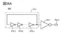
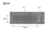
- Another aspect of the present invention is a semiconductor device including an n-stage (n is an odd number of 3 or more) inverter circuits, and the output of the i-stage (i is a natural number of 2 or more and n-1 or less) inverter circuit. Is electrically connected to the input of the i + 1th stage inverter circuit, and the output of the i-1st stage inverter circuit is electrically connected to the input of the ith stage inverter circuit.
- the semiconductor device described above preferably has a function of adjusting the voltage supplied to the second back gate according to the operating temperature.
- the present invention it is possible to provide a semiconductor device having little variation in transistor characteristics. Further, according to one aspect of the present invention, it is possible to provide a semiconductor device having a large on-current. Further, according to one aspect of the present invention, it is possible to provide a semiconductor device having good electrical characteristics. Further, according to one aspect of the present invention, it is possible to provide a semiconductor device capable of miniaturization or high integration. Further, according to one aspect of the present invention, it is possible to provide a semiconductor device having good reliability. Further, according to one aspect of the present invention, a semiconductor device having low power consumption can be provided. Further, according to one aspect of the present invention, it is possible to provide a semiconductor device that operates stably even if the operating temperature changes.
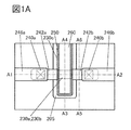
- FIG. 1A is a top view of the semiconductor device.
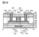
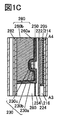
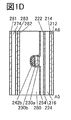
- 1B to 1D are cross-sectional views of a semiconductor device.
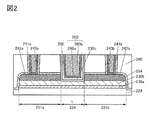
- FIG. 2 is a cross-sectional view of the semiconductor device.
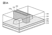
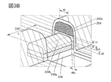
- 3A and 3B are perspective views of the semiconductor device.
- 4A to 4D are views showing a method of manufacturing a semiconductor device.
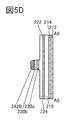
- 5A to 5D are diagrams showing a method of manufacturing a semiconductor device.
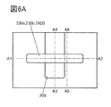
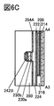
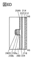
- 6A to 6D are diagrams showing a method of manufacturing a semiconductor device.
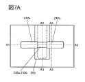
- 7A to 7D are diagrams showing a method of manufacturing a semiconductor device.
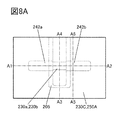
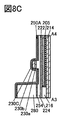
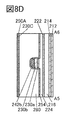
- 8A to 8D are diagrams showing a method of manufacturing a semiconductor device.
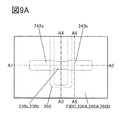
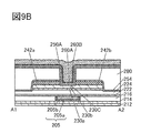
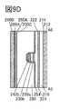
- 9A to 9D are diagrams showing a method of manufacturing a semiconductor device.
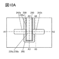
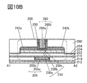
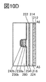
- 10A to 10D are diagrams showing a method for manufacturing a semiconductor device.
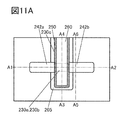
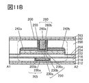
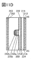
- FIG. 11A to 11D are diagrams showing a method of manufacturing a semiconductor device.
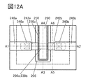
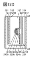
- FIG. 12A is a top view of the semiconductor device.
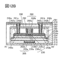
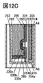
- 12B to 12D are cross-sectional views of the semiconductor device.
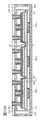
- 13A and 13B are cross-sectional views of the semiconductor device.
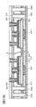
- FIG. 14 is a cross-sectional view of the semiconductor device.
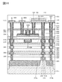
- FIG. 15 is a cross-sectional view of the semiconductor device.
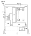
- FIG. 16A is a block diagram showing a configuration example of the storage device.
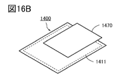
- FIG. 16B is a perspective view of the storage device.
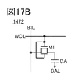
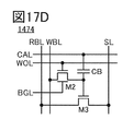
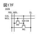
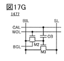
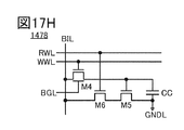
- 17A to 17H are circuit diagrams showing a configuration example of a memory cell.
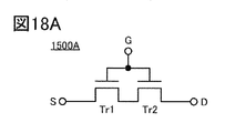
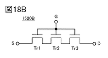
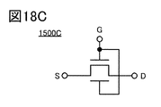
- 18A to 18D are diagrams showing circuit symbols of transistors.
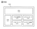
- 19A and 19B are schematic views of a semiconductor device.
- first and second ordinal numbers are used for convenience and do not indicate the process order or the stacking order. Therefore, for example, the "first” can be appropriately replaced with the “second” or “third” for explanation.
- the ordinal numbers described in the present specification and the like may not match the ordinal numbers used to specify one aspect of the present invention.
- a transistor is an element having at least three terminals including a gate, a drain, and a source. It also has a region (hereinafter, also referred to as a channel forming region) in which a channel is formed between the drain (drain terminal, drain region or drain electrode) and the source (source terminal, source region or source electrode). A current can flow between the source and the drain through the channel formation region.
- the channel formation region means a region in which a current mainly flows.
- the channel length is, for example, the source in the top view of the transistor, the region where the semiconductor (or the portion where the current flows in the semiconductor when the transistor is on) and the gate electrode overlap each other, or the channel formation region.
- the channel length does not always take the same value in all regions. That is, the channel length of one transistor may not be fixed to one value. Therefore, in the present specification, the channel length is set to any one value, the maximum value, the minimum value, or the average value in the channel formation region.
- the channel width is, for example, the channel length direction in the region where the semiconductor (or the portion where the current flows in the semiconductor when the transistor is on) and the gate electrode overlap each other in the top view of the transistor, or the channel formation region. Refers to the length of the channel formation region in the vertical direction with reference to. In one transistor, the channel width does not always take the same value in all regions. That is, the channel width of one transistor may not be fixed to one value. Therefore, in the present specification, the channel width is set to any one value, the maximum value, the minimum value, or the average value in the channel formation region.
- the channel width in the region where the channel is actually formed (hereinafter, also referred to as “effective channel width”) and the channel width shown in the top view of the transistor. (Hereinafter, also referred to as “apparent channel width”) and may be different.
- the effective channel width may be larger than the apparent channel width, and the influence thereof may not be negligible.
- the proportion of the channel forming region formed on the side surface of the semiconductor may be large. In that case, the effective channel width is larger than the apparent channel width.
- channel width may refer to an apparent channel width.
- channel width may refer to an effective channel width.
- the channel length, channel width, effective channel width, apparent channel width, and the like can be determined by analyzing a cross-sectional TEM image or the like.
- the semiconductor impurities are, for example, other than the main components constituting the semiconductor.
- an element having a concentration of less than 0.1 atomic% can be said to be an impurity. Due to the inclusion of impurities, for example, the defect level density of the semiconductor may increase or the crystallinity may decrease.
- the impurities that change the characteristics of the semiconductor include, for example, Group 1 elements, Group 2 elements, Group 13 elements, Group 14 elements, Group 15 elements, and oxide semiconductors.
- transition metals other than the main component such as hydrogen, lithium, sodium, silicon, boron, phosphorus, carbon, and nitrogen. Water may also function as an impurity.
- the oxide semiconductor to an oxygen vacancy V O: also referred to as oxygen vacancy
- normally off means that when a potential is not applied to the gate or a ground potential is applied to the gate, the drain current per 1 ⁇ m of the channel width flowing through the transistor is 1 ⁇ 10 ⁇ at room temperature. It means that it is 20 A or less, 1 ⁇ 10 -18 A or less at 85 ° C, or 1 ⁇ 10 -16 A or less at 125 ° C.
- the high power potential Vdd (hereinafter, also simply referred to as “Vdd”, “H potential”, or “H”) refers to the low power potential Vss (hereinafter, simply “Vss”, “L potential”). , Or also referred to as “L”), indicating a power supply potential with a higher potential. Further, Vss indicates a power supply potential having a potential lower than Vdd.
- the ground potential can also be used as Vdd or Vss. For example, when Vdd is the ground potential, Vss is a potential lower than the ground potential, and when V stability is the ground potential, Vdd is a potential higher than the ground potential.
- conductor 240 (conductor 240a and conductor 240b) that is electrically connected to the transistor 200 and functions as a plug.
- An insulator 241 (insulator 241a and insulator 241b) is provided in contact with the side surface of the conductor 240 that functions as a plug.
- a conductor 246 (conductor 246a and a conductor 246b) that is electrically connected to the conductor 240 and functions as wiring is provided.
- a first conductor of 240b is provided, and a second conductor of the conductor 240b is further provided inside.
- the height of the upper surface of the conductor 240 and the height of the upper surface of the insulator 281 can be made about the same.
- the transistor 200 shows a configuration in which the first conductor of the conductor 240 and the second conductor of the conductor 240 are laminated, but the present invention is not limited to this.
- the conductor 240 may be provided as a single layer or a laminated structure having three or more layers. When the structure has a laminated structure, an ordinal number may be given in the order of formation to distinguish them.
- the oxide 230c has a region in contact with the oxide 230b, a region overlapping with the side surface of the conductor 260 via the insulator 250, and a bottom surface of the conductor 260 via the insulator 250. Has a region that overlaps with.
- an In-M-Zn oxide having indium, element M and zinc (element M is aluminum, gallium, yttrium, tin, copper, vanadium, beryllium, boron, titanium, iron, nickel, germanium). , Zirconium, molybdenum, lanthanum, cerium, neodymium, hafnium, tantalum, tungsten, magnesium, etc. (one or more) and the like may be used. Further, as the oxide 230, an In—Ga oxide or an In—Zn oxide may be used.
- the oxide 230a and the oxide 230b and the oxide 230b and the oxide 230c have a common element other than oxygen as a main component.
- the defect level density at the interface between the oxide 230a and the oxide 230b and the interface between the oxide 230b and the oxide 230c can be lowered. Therefore, the influence of interfacial scattering on carrier conduction is reduced, and the transistor 200 can obtain a large on-current and high frequency characteristics.
- the conductor 260 has a conductor 260a and a conductor 260b, and the conductor 260a is arranged so as to wrap the bottom surface and the side surface of the conductor 260b.
- the conductor 260 functions as a first gate (also referred to as a top gate) electrode of the transistor 200.
- the resistance of the oxide semiconductor may be lowered.
- the electrical characteristics are liable to fluctuate, and reliability may deteriorate.
- the impurities include aluminum (Al) and silicon (Si).
- Aluminum and silicon have higher binding energies with oxygen than indium and zinc.
- In-M-Zn oxide when aluminum is mixed in the oxide semiconductor, oxygen contained in the oxide semiconductor is deprived by aluminum, so that oxygen is absorbed in the vicinity of indium or zinc. Defects may form.
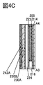
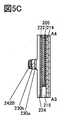
- the oxide 230b has a region 231a (not shown in FIG. 3B) in contact with at least a part of the conductor 242a, a region 231b (not shown in FIG. 3B) in contact with at least a part of the conductor 242b, and a region. Between the 231a and the region 231b, there is a region 234 that functions as a channel forming region of the transistor 200.
- the region 234 has a region in which the oxide 230b and the conductor 260 overlap with each other in the oxide 230b.
- the region where the oxide 230b and the conductor 242a overlap can be rephrased as the region 231a, and the region where the oxide 230b and the conductor 242b overlap can be rephrased as the region 231b. ..
- the end portion of the side surface and the end portion of the upper surface are curved (hereinafter, also referred to as a round shape).
- the radius of curvature on the curved surface is La.
- La is the height of the upper surface of the oxide 230b in the region where the oxide 230b and the conductor 260 overlap when the lower surface of the insulator 224 is used as a reference in the cross-sectional view of the transistor 200 in the channel width direction.
- the side surface of the oxide 230b it may be regarded as the difference from the height of the lower end portion of the region having the curved surface.
- the transistor when impurities are mixed in the oxide semiconductor, a defect level or an oxygen defect may be formed. Therefore, when impurities are mixed in the channel formation region of the oxide semiconductor, the electrical characteristics of the transistor using the oxide semiconductor are liable to fluctuate, and the reliability may be deteriorated. Further, when the channel formation region contains oxygen deficiency, the transistor tends to have a normal-on characteristic (a characteristic that a channel exists even if a voltage is not applied to the gate electrode and a current flows through the transistor).
- the upper surface of the oxide 230b in the region 234 is lower than the upper surface of the oxide 230b in the region overlapping the conductor 242.
- Lc is preferably larger than 0 nm and smaller than the film thickness of the oxide 230b in the region overlapping the conductor 242.
- Lc is larger than 0 nm and 15 nm or less, preferably 0.5 nm or more and 10 nm or less, and more preferably 1 nm or more and 5 nm or less.
- the effective channel length on the upper surface of the region 234 is L + 2 ⁇ Lc. Therefore, by reducing Lc, it is possible to suppress a decrease in the on-current of the transistor.
- the amount of film loss on the side surface of the oxide 230b in the region where the oxide 230b and the conductor 260 overlap is defined as We.
- We is calculated as, for example, the difference between the side surface of the oxide 230b in the region overlapping the conductor 242 and the side surface of the oxide 230b in the region having no curved surface in the cross-sectional view of the transistor 200 in the channel width direction. can do.
- the difference between the length of the lower surface of the oxide 230b in the region overlapping the conductor 242 and the length of the lower surface of the oxide 230b in the region not overlapping the conductor 242. Can be calculated as half of.
- x i is the value of Vsh of the i-th transistor (i is an integer of 1 or more and n or less), and ⁇ is the average value of Vsh of n transistors.
- the standard deviation ⁇ of Vsh is specifically 60 mV or less, preferably 40 mV or less, and more preferably 20 mV or less.
- the impurity concentration in the channel forming region of the oxide semiconductor and its vicinity can be reduced.
- the concentration of impurities obtained by secondary ion mass spectrometry (SIMS) in the channel formation region of the oxide semiconductor and its vicinity is preferably 1 ⁇ 10 18 atoms / cm 3 or less. Is 2 ⁇ 10 16 atoms / cm 3 or less.
- the concentration of impurities obtained by elemental analysis using energy dispersive X-ray spectroscopy (EDX) in the channel formation region of the oxide semiconductor and its vicinity is reduced to 1.0 atomic% or less. To do.
- the concentration ratio of impurities to the element M is set to less than 0.10, preferably less than 0.05 in the channel formation region of the oxide semiconductor and its vicinity. ..
- the concentration of the element M used when calculating the concentration ratio may be the concentration in the same region as the region in which the concentration of impurities is calculated, or may be the concentration in the oxide semiconductor.
- the insulator 212, the insulator 214, the insulator 254, the insulator 282, the insulator 283 and the insulator 281 a hydrogen atom, a hydrogen molecule, a water molecule, a nitrogen atom, a nitrogen molecule, nitric oxide molecule (N 2 O)
- an insulating material having a function of suppressing the diffusion of impurities such as NO, NO 2
- copper atoms the above impurities are difficult to permeate
- it is preferable to use an insulating material having a function of suppressing the diffusion of oxygen for example, at least one oxygen atom, oxygen molecule, etc.) (the oxygen is difficult to permeate).
- the transistor 200 is surrounded by an insulator 212, an insulator 214, an insulator 254, an insulator 282, and an insulator 283 having a function of suppressing the diffusion of impurities such as water and hydrogen, and oxygen. Is preferable.
- the conductor 260 may function as a first gate (also referred to as a top gate) electrode. Further, the conductor 205 may function as a second gate electrode. In that case, the threshold voltage (Vth) of the transistor 200 can be controlled by changing the potential applied to the conductor 205 independently of the potential applied to the conductor 260 without interlocking with it. In particular, by applying a negative potential to the conductor 205, it is possible to increase the Vth of the transistor 200 and reduce the off-current. Therefore, when a negative potential is applied to the conductor 205, the drain current when the potential applied to the conductor 260 is 0 V can be made smaller than when it is not applied.
- Vth threshold voltage
- the conductor 205 may be provided larger than the size of the region that does not overlap with the conductor 242a and the conductor 242b of the oxide 230.
- the conductor 205 is also stretched in a region outside the end portion intersecting the channel width direction of the oxide 230. That is, it is preferable that the conductor 205 and the conductor 260 are superimposed via an insulator on the outside of the side surface of the oxide 230 in the channel width direction.
- the channel forming region of the oxide 230 is electrically surrounded by the electric field of the conductor 260 that functions as the first gate electrode and the electric field of the conductor 205 that functions as the second gate electrode. Can be done.
- the structure of the transistor that electrically surrounds the channel forming region by the electric fields of the first gate and the second gate is referred to as a surroundd channel (S-channel) structure.
- the transistor having the S-channel structure represents the structure of the transistor that electrically surrounds the channel forming region by the electric fields of one and the other of the pair of gate electrodes.
- the side surface and the periphery of the oxide 230 in contact with the conductor 242a and the conductor 242b functioning as the source electrode and the drain electrode are said to be type I as in the channel forming region. It has characteristics. Further, since the side surface and the periphery of the oxide 230 in contact with the conductor 242a and the conductor 242b are in contact with the insulator 280, they can be type I as in the channel formation region.
- type I can be treated as the same as high-purity authenticity described later.
- the S-channel structure disclosed in the present specification and the like is different from the Fin type structure and the planar type structure. By adopting the S-channel structure, it is possible to increase the resistance to the short-channel effect, in other words, to make a transistor in which the short-channel effect is unlikely to occur.
- the conductor 205 is stretched to function as wiring.
- the present invention is not limited to this, and a conductor that functions as wiring may be provided under the conductor 205. Further, it is not always necessary to provide one conductor 205 for each transistor. For example, the conductor 205 may be shared by a plurality of transistors.
- the conductor 205 shows a configuration in which the conductor 205a and the conductor 205b are laminated, but the present invention is not limited to this.
- the conductor 205 may be provided as a single layer or a laminated structure having three or more layers. When the structure has a laminated structure, an ordinal number may be given in the order of formation to distinguish them.
- the conductor 205a By using a conductive material having a function of suppressing the diffusion of oxygen for the conductor 205a, it is possible to prevent the conductor 205b from being oxidized and the conductivity from being lowered.
- the conductive material having a function of suppressing the diffusion of oxygen for example, tantalum, tantalum nitride, ruthenium, ruthenium oxide and the like are preferably used. Therefore, as the conductor 205a, the conductive material may be a single layer or a laminated material.
- the conductor 205a may be a laminate of tantalum, tantalum nitride, ruthenium, or ruthenium oxide and titanium or titanium nitride.
- the conductor 205b it is preferable to use a conductive material containing tungsten, copper, or aluminum as a main component.
- a conductive material containing tungsten, copper, or aluminum as a main component.
- the conductor 205b is shown as a single layer, it may have a laminated structure, for example, titanium or titanium nitride may be laminated with the conductive material.
- the insulator 222 it is preferable to use an insulator containing oxides of one or both of aluminum and hafnium, which are insulating materials.
- the insulator it is preferable to use aluminum oxide, hafnium oxide, an oxide containing aluminum and hafnium (hafnium aluminate) and the like.
- the insulator 222 releases oxygen from the oxide 230 to the substrate side and diffuses impurities such as hydrogen from the peripheral portion of the transistor 200 to the oxide 230. Functions as a layer that suppresses.
- the insulator 222 it is possible to suppress the diffusion of impurities such as hydrogen into the inside of the transistor 200 and suppress the generation of oxygen deficiency in the oxide 230. Further, it is possible to suppress the conductor 205 from reacting with the oxygen contained in the insulator 224 and the oxide 230.
- aluminum oxide, bismuth oxide, germanium oxide, niobium oxide, silicon oxide, titanium oxide, tungsten oxide, yttrium oxide, and zirconium oxide may be added to the insulator.
- these insulators may be nitrided.
- the insulator 222 may be used by laminating silicon oxide, silicon oxide or silicon nitride on these insulators.
- the insulator 222 includes, for example, aluminum oxide, hafnium oxide, tantalum oxide, zirconium oxide, lead zirconate titanate (PZT), strontium titanate (SrTIO 3 ), (Ba, Sr) TiO 3 (BST) and the like. Insulators containing so-called high-k materials may be used in single layers or in layers. As the miniaturization and high integration of transistors progress, problems such as leakage current may occur due to the thinning of the gate insulator. By using a high-k material for an insulator that functions as a gate insulator, it is possible to reduce the gate potential during transistor operation while maintaining the physical film thickness.
- the insulator 224 in contact with the oxide 230 preferably desorbs oxygen by heating.
- the insulator 224 silicon oxide, silicon oxide nitride, or the like may be appropriately used.
- Oxygen that desorbs oxygen by heating is an oxide having a desorption amount of oxygen molecules of 1.0 ⁇ 10 18 molecules / cm 3 or more, preferably 1.0 ⁇ 10 19 molecules, as determined by TDS (Thermal Desorption Spectroscopy) analysis. It is an oxide film having a / cm 3 or more, more preferably 2.0 ⁇ 10 19 molecules / cm 3 or more, or 3.0 ⁇ 10 20 molecules / cm 3 or more.
- the surface temperature of the film during the TDS analysis is preferably in the range of 100 ° C. or higher and 700 ° C. or lower, or 100 ° C. or higher and 400 ° C. or lower.
- the insulator having the excess oxygen region and the oxide 230 may be brought into contact with each other to perform one or more of heat treatment, microwave treatment, or RF (Radio Frequency) treatment.
- heat treatment microwave treatment
- RF Radio Frequency
- water or hydrogen in the oxide 230 can be removed.
- a reaction bond defects that contains hydrogen to an oxygen vacancy (V O H) is cut occurs, a reaction occurs that when other words "V O H ⁇ V O + H", dehydrogenation Can be transformed into.
- the hydrogen generated as oxygen combines with H 2 O, it may be removed from the oxide 230 or oxide 230 near the insulator.
- a part of hydrogen may be diffused or captured (also referred to as gettering) in the conductor 242.
- oxygen and argon are used as the gas to be introduced into the apparatus for performing microwave treatment, and the oxygen flow rate ratio (O 2 / (O 2 + Ar)) is 50% or less, preferably 10% or more and 30. It is recommended to use less than%.
- the heat treatment may be performed, for example, at 100 ° C. or higher and 450 ° C. or lower, more preferably 350 ° C. or higher and 400 ° C. or lower.
- the heat treatment is carried out in an atmosphere of nitrogen gas or an inert gas, or an atmosphere containing 10 ppm or more, 1% or more, or 10% or more of an oxidizing gas.
- the heat treatment is preferably performed in an oxygen atmosphere.
- oxygen can be supplied to the oxide 230 to reduce oxygen deficiency ( VO ).
- the heat treatment may be performed in a reduced pressure state.
- the heat treatment may be carried out in an atmosphere containing 10 ppm or more, 1% or more, or 10% or more of oxidizing gas in order to supplement the desorbed oxygen after the heat treatment in an atmosphere of nitrogen gas or an inert gas.
- the heat treatment may be performed in an atmosphere containing 10 ppm or more, 1% or more, or 10% or more of the oxidizing gas, and then the heat treatment may be continuously performed in an atmosphere of nitrogen gas or an inert gas.
- the insulator 222 and the insulator 224 may have a laminated structure of two or more layers.
- the laminated structure is not limited to the same material, and may be a laminated structure made of different materials.
- the oxide 230 preferably has a laminated structure of a plurality of oxide layers having different chemical compositions.
- the atomic number ratio of the element M to the metal element as the main component is the ratio of the element M to the metal element as the main component in the metal oxide used for the oxide 230b. It is preferably larger than the atomic number ratio.
- the atomic number ratio of the element M to In is preferably larger than the atomic number ratio of the element M to In in the metal oxide used for the oxide 230b.
- the atomic number ratio of In to the element M is preferably larger than the atomic number ratio of In to the element M in the metal oxide used for the oxide 230a.
- the oxide 230c a metal oxide that can be used for the oxide 230a or the oxide 230b can be used.
- In-Zn oxide for the oxide 230.
- In-Zn oxide for the oxide 230, for example, a laminated structure using In-Zn oxide for the oxide 230a and In-M-Zn oxide for the oxide 230b and the oxide 230c, or oxidation. Examples thereof include a laminated structure in which an In—M—Zn oxide is used for the object 230a and an In—Zn oxide is used for either the oxide 230b or the oxide 230c.
- the lower end of the conduction band changes gently.
- the lower end of the conduction band at the junction of the oxide 230a, the oxide 230b, and the oxide 230c is continuously changed or continuously bonded.
- the oxide 230a and the oxide 230b and the oxide 230b and the oxide 230c have a common element as a main component other than oxygen, a mixed layer having a low defect level density can be formed. ..
- the oxide 230b is an In-Ga-Zn oxide, In-Ga-Zn oxide, Ga-Zn oxide, gallium oxide or the like may be used as the oxide 230a and the oxide 230c.
- the above atomic number ratio is not limited to the atomic number ratio of the formed metal oxide, but is the atomic number ratio of the sputtering target used for forming the metal oxide. It may be.
- Examples of the conductors 242 include nitrides containing tantalum, nitrides containing titanium, nitrides containing molybdenum, nitrides containing tungsten, and nitrides containing tantalum and aluminum. It is preferable to use a nitride containing titanium and aluminum. In one aspect of the invention, tantalum-containing nitrides are particularly preferred. Further, for example, ruthenium oxide, ruthenium nitride, an oxide containing strontium and ruthenium, an oxide containing lantern and nickel, and the like may be used. These materials are preferable because they are conductive materials that are difficult to oxidize or materials that maintain conductivity even when oxygen is absorbed.
- hydrogen contained in the oxide 230b or the like may diffuse into the conductor 242a or the conductor 242b.
- hydrogen contained in the oxide 230b or the like may diffuse into the conductor 242a or the conductor 242b.
- hydrogen contained in the oxide 230b or the like is easily diffused to the conductor 242a or the conductor 242b, and the diffused hydrogen is the conductor. It may bind to the nitrogen contained in the 242a or the conductor 242b. That is, hydrogen contained in the oxide 230b or the like may be absorbed by the conductor 242a or the conductor 242b.
- the insulator 254 is preferably formed by a sputtering method.
- oxygen can be added to the vicinity of the region of the insulator 224 in contact with the insulator 254.
- oxygen can be supplied from the region into the oxide 230 via the insulator 224.
- the insulator 254 has a function of suppressing the diffusion of oxygen upward, it is possible to prevent oxygen from diffusing from the oxide 230 to the insulator 280.
- the insulator 222 has a function of suppressing the diffusion of oxygen downward, it is possible to prevent oxygen from diffusing from the oxide 230 toward the substrate side. In this way, oxygen is supplied to the channel forming region of the oxide 230. As a result, the oxygen deficiency of the oxide 230 can be reduced and the normalization of the transistor can be suppressed.
- the insulator 254 for example, an insulator containing aluminum nitride may be used. As a result, a film having excellent insulating properties and excellent thermal conductivity can be formed, so that the heat dissipation of heat generated when the transistor 200 is driven can be enhanced. Further, silicon nitride, silicon nitride oxide and the like can also be used.
- the insulator 254 can have a multi-layer structure having two or more layers.
- the film formation of the lower layer and the upper layer of the insulator 254 can be performed by using the above method, and the film formation of the lower layer and the upper layer of the insulator 254 can be performed.
- the same method may be used, or different methods may be used.
- the lower layer of the insulator 254 may be formed by a sputtering method in an atmosphere containing oxygen, and then the upper layer of the insulator 254 may be formed by using the ALD method. Since the ALD method is a film forming method having good coverage, it is possible to prevent the formation of step breaks or the like due to the unevenness of the first layer.
- the above materials can be used for the lower layer and the upper layer of the insulator 254, and the lower layer and the upper layer of the insulator 254 may be the same material or different materials.
- it may be a laminated structure of silicon oxide, silicon oxide nitride, silicon nitride or silicon nitride, and an insulator having a function of suppressing the permeation of impurities such as hydrogen and oxygen.
- an insulator having a function of suppressing the permeation of impurities such as hydrogen and oxygen for example, an insulator containing an oxide of one or both of aluminum and hafnium can be used.
- the insulator 250 functions as a gate insulator.
- the insulator 250 is preferably arranged in contact with at least a part of the oxide 230c.
- the insulator 250 includes silicon oxide, silicon oxide, silicon nitride, silicon nitride, silicon oxide added with fluorine, silicon oxide added with carbon, silicon oxide added with carbon and nitrogen, silicon oxide having pores, and the like. Can be used. In particular, silicon oxide and silicon nitride nitride are preferable because they are stable against heat.
- the insulator 250 is preferably formed by using an insulator that releases oxygen by heating.
- an insulator that releases oxygen by heating as an insulator 250 in contact with at least a part of the oxide 230c, oxygen can be effectively supplied to the channel forming region of the oxide 230b, and the oxide 230b can be provided with oxygen. Oxygen deficiency in the channel formation region can be reduced. Therefore, it is possible to provide a transistor that suppresses fluctuations in electrical characteristics, has stable electrical characteristics, and has improved reliability.
- the concentration of impurities such as water and hydrogen in the insulator 250 is reduced.
- the film thickness of the insulator 250 is preferably 1 nm or more and 20 nm or less.
- the insulator 250 is shown as a single layer in FIG. 1, it may have a laminated structure of two or more layers.
- the lower layer of the insulator 250 is formed by using an insulator that releases oxygen by heating, and the upper layer of the insulator 250 has a function of suppressing the diffusion of oxygen. It is preferable to form using an insulator having. With such a configuration, oxygen contained in the lower layer of the insulator 250 can be suppressed from diffusing into the conductor 260. That is, it is possible to suppress a decrease in the amount of oxygen supplied to the oxide 230. Further, it is possible to suppress the oxidation of the conductor 260 by oxygen contained in the lower layer of the insulator 250.
- the lower layer of the insulator 250 can be provided by using a material that can be used for the insulator 250 described above, and the upper layer of the insulator 250 can be provided by using the same material as the insulator 222.
- an insulating material which is a high-k material having a high relative permittivity may be used for the upper layer of the insulator 250.
- the gate insulator By forming the gate insulator into a laminated structure of the lower layer of the insulator 250 and the upper layer of the insulator 250, it is possible to obtain a laminated structure that is stable against heat and has a high relative permittivity. Therefore, it is possible to reduce the gate potential applied during transistor operation while maintaining the physical film thickness of the gate insulator.
- the equivalent oxide film thickness (EOT) of the insulator that functions as the gate insulator can be thinned.
- a thing or a metal oxide that can be used as the oxide 230 can be used.
- a metal oxide may be provided between the insulator 250 and the conductor 260.
- the metal oxide preferably suppresses the diffusion of oxygen from the insulator 250 to the conductor 260.
- the diffusion of oxygen from the insulator 250 to the conductor 260 is suppressed. That is, it is possible to suppress a decrease in the amount of oxygen supplied to the oxide 230.
- the oxidation of the conductor 260 by oxygen of the insulator 250 can be suppressed.
- the metal oxide preferably has a function as a part of the first gate electrode.
- a metal oxide that can be used as the oxide 230 can be used as the metal oxide.
- the conductor 260a into a film by a sputtering method, the electric resistance value of the metal oxide can be lowered to form a conductor.
- This can be called an OC (Oxide Conductor) electrode.
- it can be used as the metal oxide by lowering the resistance of the oxide semiconductor that can be used for the oxide 230.
- the upper layer of the insulator 250 and / or the metal oxide By having the upper layer of the insulator 250 and / or the metal oxide, it is possible to improve the on-current of the transistor 200 without weakening the influence of the electric field from the conductor 260. Further, by keeping the distance between the conductor 260 and the oxide 230 due to the physical thickness of the insulator 250 and the metal oxide, the leakage current between the conductor 260 and the oxide 230 is maintained. Can be suppressed. Further, by providing the laminated structure of the insulator 250 and the metal oxide, the physical distance between the conductor 260 and the oxide 230 and the electric field strength applied from the conductor 260 to the oxide 230 can be determined. It can be easily adjusted as appropriate.
- the conductor 260a it is preferable to use a conductive material having a function of suppressing the diffusion of impurities such as hydrogen atom, hydrogen molecule, water molecule, nitrogen atom, nitrogen molecule, nitrogen oxide molecule and copper atom.
- impurities such as hydrogen atom, hydrogen molecule, water molecule, nitrogen atom, nitrogen molecule, nitrogen oxide molecule and copper atom.
- a conductive material having a function of suppressing the diffusion of oxygen for example, at least one oxygen atom, oxygen molecule, etc.
- the conductor 260a has a function of suppressing the diffusion of oxygen, it is possible to prevent the conductor 260b from being oxidized by the oxygen contained in the insulator 250 to reduce the conductivity.
- the conductive material having a function of suppressing the diffusion of oxygen for example, tantalum, tantalum nitride, ruthenium, ruthenium oxide and the like are preferably used.
- the upper surface of the conductor 260 substantially coincides with the upper surface of the insulator 250 and the upper surface of the oxide 230c.
- the height is preferably lower than the height of the bottom surface of the oxide 230b.
- the conductor 260 which functions as a gate electrode, covers the side surface and the upper surface of the channel forming region of the oxide 230b via an insulator 250 or the like, so that the electric field of the conductor 260 is covered with the channel forming region of the oxide 230b. It becomes easier to act on the whole. Therefore, the on-current of the transistor 200 can be increased and the frequency characteristics can be improved.
- the difference is 0 nm or more and 100 nm or less, preferably 3 nm or more and 50 nm or less, and more preferably 5 nm or more and 20 nm or less.
- the insulator 280 is provided on the insulator 224, the oxide 230a, the oxide 230b, the conductor 242, and the insulator 254. Further, the upper surface of the insulator 280 may be flattened.
- the insulator 280 that functions as an interlayer film preferably has a low dielectric constant.
- a material having a low dielectric constant as an interlayer film, it is possible to reduce the parasitic capacitance generated between the wirings.
- the insulator 280 is provided by using the same material as the insulator 216, for example.
- silicon oxide and silicon oxide nitride are preferable because they are thermally stable.
- materials such as silicon oxide, silicon oxide nitride, and silicon oxide having pores are preferable because a region containing oxygen desorbed by heating can be easily formed.
- the concentration of impurities such as water and hydrogen in the insulator 280 is reduced.
- the insulator 280 preferably has a low hydrogen concentration and an excess oxygen region or an excess oxygen, and may be provided by using the same material as the insulator 216, for example.
- the insulator 280 may have a structure in which the above materials are laminated, and is formed by, for example, silicon oxide formed by a sputtering method and a chemical vapor deposition (CVD) method laminated on the silicon oxide. It may be a laminated structure of filmed silicon oxide. Further, silicon nitride may be further laminated on top of it.
- the insulator 274 that functions as an interlayer film on the insulator 282.
- the insulator 274 preferably has a reduced concentration of impurities such as water or hydrogen in the film.
- the conductor 240a and the conductor 240b it is preferable to use a conductive material containing tungsten, copper, or aluminum as a main component. Further, the conductor 240a and the conductor 240b may have a laminated structure.
- the conductive material By using the conductive material, it is possible to prevent oxygen added to the insulator 280 from being absorbed by the conductor 240a and the conductor 240b. In addition, impurities such as water and hydrogen contained in the layer above the insulator 281 can be suppressed from being mixed into the oxide 230 through the conductor 240a and the conductor 240b.
- an insulator such as silicon nitride, aluminum oxide, or silicon nitride may be used. Since the insulator 241a and the insulator 241b are provided in contact with the insulator 254, impurities such as water and hydrogen contained in the insulator 280 and the like are prevented from being mixed into the oxide 230 through the conductor 240a and the conductor 240b. It can be suppressed.
- silicon nitride is suitable because it has a high blocking property against hydrogen. Further, it is possible to prevent oxygen contained in the insulator 280 from being absorbed by the conductor 240a and the conductor 240b.
- an insulator substrate for example, an insulator substrate, a semiconductor substrate, or a conductor substrate may be used.
- the insulator substrate include a glass substrate, a quartz substrate, a sapphire substrate, a stabilized zirconia substrate (yttria-stabilized zirconia substrate, etc.), a resin substrate, and the like.
- the semiconductor substrate include a semiconductor substrate made of silicon, germanium and the like, and a compound semiconductor substrate made of silicon carbide, silicon germanium, gallium arsenide, indium phosphide, zinc oxide and gallium oxide.
- the conductor substrate includes a graphite substrate, a metal substrate, an alloy substrate, and a conductive resin substrate.
- a substrate having a metal nitride a substrate having a metal oxide, and the like.
- a substrate in which a conductor or a semiconductor is provided in an insulator substrate a substrate in which a conductor or an insulator is provided in a semiconductor substrate, a substrate in which a semiconductor or an insulator is provided in a conductor substrate, and the like.
- those substrates provided with elements may be used.
- Elements provided on the substrate include capacitive elements, resistance elements, switch elements, light emitting elements, storage elements, and the like.
- Insulator examples include oxides, nitrides, oxide nitrides, nitride oxides, metal oxides, metal oxide nitrides, and metal nitride oxides having insulating properties.
- Examples of the insulator having a high specific dielectric constant include gallium oxide, hafnium oxide, zirconium oxide, oxides having aluminum and hafnium, nitrides having aluminum and hafnium, oxides having silicon and hafnium, silicon and hafnium. There are nitrides having oxides, or nitrides having silicon and hafnium.
- Examples of insulators having a low relative permittivity include silicon oxide, silicon oxide, silicon nitride, silicon nitride, silicon oxide with fluorine added, silicon oxide with carbon added, silicon oxide with carbon and nitrogen added, and empty. There are silicon oxide having holes, resin, and the like.
- the electric characteristics of the transistor can be stabilized by surrounding the transistor using the metal oxide with an insulator having a function of suppressing the permeation of impurities such as hydrogen and oxygen.
- the insulator having a function of suppressing the permeation of impurities such as hydrogen and oxygen include boron, carbon, nitrogen, oxygen, fluorine, magnesium, aluminum, silicon, phosphorus, chlorine, argon, gallium, germanium, yttrium, and zirconium. Insulators containing, lanthanum, neodymium, hafnium, or tantalum may be used in single layers or in layers.
- an insulator having a function of suppressing the permeation of impurities such as hydrogen and oxygen
- Metal oxides such as tantalum oxide and metal nitrides such as aluminum nitride, silicon nitride and silicon nitride can be used.
- the insulator that functions as a gate insulator is preferably an insulator having a region containing oxygen that is desorbed by heating.
- the oxygen deficiency of the oxide 230 can be compensated.
- Conductors include aluminum, chromium, copper, silver, gold, platinum, tantalum, nickel, titanium, molybdenum, tungsten, hafnium, vanadium, niobium, manganese, magnesium, zirconium, beryllium, indium, ruthenium, iridium, strontium, and lanthanum. It is preferable to use a metal element selected from the above, an alloy containing the above-mentioned metal element as a component, an alloy in which the above-mentioned metal element is combined, or the like.
- tantalum nitride, titanium nitride, tungsten, nitrides containing titanium and aluminum, nitrides containing tantalum and aluminum, ruthenium oxide, ruthenium nitride, oxides containing strontium and ruthenium, oxides containing lanthanum and nickel, etc. are used. Is preferable.
- tantalum nitride, titanium nitride, nitrides containing titanium and aluminum, nitrides containing tantalum and aluminum, ruthenium oxide, ruthenium nitride, oxides containing strontium and ruthenium, and oxides containing lanthanum and nickel are difficult to oxidize.
- the conductor functioning as the gate electrode shall have a laminated structure in which the above-mentioned material containing a metal element and a conductive material containing oxygen are combined. Is preferable.
- a conductive material containing oxygen may be provided on the channel forming region side.
- the conductor that functions as the gate electrode it is preferable to use a conductive material containing a metal element and oxygen contained in the metal oxide in which the channel is formed.
- the above-mentioned conductive material containing a metal element and nitrogen may be used.
- a conductive material containing nitrogen such as titanium nitride and tantalum nitride may be used.
- indium tin oxide, indium oxide containing tungsten oxide, indium zinc oxide containing tungsten oxide, indium oxide containing titanium oxide, indium tin oxide containing titanium oxide, indium zinc oxide, and silicon were added.
- Indium tin oxide may be used.
- indium gallium zinc oxide containing nitrogen may be used.
- the metal oxide is an In-M-Zn oxide having indium, the element M, and zinc.
- the element M is aluminum, gallium, yttrium, or tin.
- elements applicable to the other element M include boron, titanium, iron, nickel, germanium, zirconium, molybdenum, lanthanum, cerium, neodymium, hafnium, tantalum, tungsten, and magnesium.
- the element M a plurality of the above-mentioned elements may be combined in some cases.
- a metal oxide having nitrogen may also be generically referred to as a metal oxide. Further, a metal oxide having nitrogen may be referred to as a metal oxynitride.
- CAAC-OS has a c-axis orientation and has a distorted crystal structure in which a plurality of nanocrystals are connected in the ab plane direction.
- the strain refers to a region in which a plurality of nanocrystals are connected, in which the orientation of the lattice arrangement changes between a region in which the lattice arrangement is aligned and a region in which another lattice arrangement is aligned.
- nanocrystals are basically hexagonal, they are not limited to regular hexagons and may have non-regular hexagons. Further, in distortion, it may have a lattice arrangement such as a pentagon or a heptagon.
- CAAC-OS it is difficult to confirm a clear grain boundary even in the vicinity of strain. That is, it can be seen that the formation of grain boundaries is suppressed by the distortion of the lattice arrangement. This is because CAAC-OS can tolerate distortion because the arrangement of oxygen atoms is not dense in the ab plane direction and the bond distance between atoms changes due to substitution of metal elements. Because.
- CAAC-OS is a layered crystal in which a layer having indium and oxygen (hereinafter, In layer) and a layer having elements M, zinc, and oxygen (hereinafter, (M, Zn) layer) are laminated. It tends to have a structure (also called a layered structure). Indium and the element M can be replaced with each other, and when the element M of the (M, Zn) layer is replaced with indium, it can be expressed as the (In, M, Zn) layer. Further, when the indium of the In layer is replaced with the element M, it can be expressed as the (In, M) layer.
- the nc-OS has periodicity in the atomic arrangement in a minute region (for example, a region of 1 nm or more and 10 nm or less, particularly a region of 1 nm or more and 3 nm or less).
- nc-OS does not show regularity in crystal orientation between different nanocrystals. Therefore, no orientation is observed in the entire film. Therefore, nc-OS may be indistinguishable from a-like OS and amorphous oxide semiconductors depending on the analysis method.
- In-Ga-Zn oxide which is a kind of metal oxide having indium, gallium, and zinc, may have a stable structure by forming the above-mentioned nanocrystals. is there.
- IGZO tends to have difficulty in crystal growth in the atmosphere, it is recommended to use smaller crystals (for example, the above-mentioned nanocrystals) than large crystals (here, a few mm crystal or a few cm crystal). However, it may be structurally stable.
- the a-like OS is a metal oxide having a structure between the nc-OS and an amorphous oxide semiconductor.
- the a-like OS has a void or low density region. That is, the a-like OS has lower crystallinity than the nc-OS and CAAC-OS.
- Oxide semiconductors have various structures, and each has different characteristics.
- the oxide semiconductor of one aspect of the present invention may have two or more of amorphous oxide semiconductor, polycrystalline oxide semiconductor, a-like OS, nc-OS, and CAAC-OS.
- a transistor using a metal oxide fluctuates its electrical characteristics due to impurities and oxygen deficiency in the metal oxide, and has normal-on characteristics (channels exist even if no voltage is applied to the gate electrode, and current is applied to the transistor. (Characteristics of flowing). Further, when the transistor is driven in a state where the metal oxide contains excess oxygen exceeding an appropriate amount value, the valence of the excess oxygen atom changes and the electrical characteristics of the transistor fluctuate. , May be unreliable.
- the carrier concentration of the metal oxide in the channel formation region is preferably 1 ⁇ 10 18 cm -3 or less, more preferably 1 ⁇ 10 17 cm -3 or less, and 1 ⁇ 10 16 cm -3. It is more preferably less than 1 ⁇ 10 13 cm -3 , further preferably less than 1 ⁇ 10 12 cm -3 .
- the lower limit of the carrier concentration of the metal oxide in the channel formation region is not particularly limited, but may be, for example, 1 ⁇ 10 -9 cm -3 .
- impurities in the metal oxide include hydrogen, nitrogen, alkali metal, alkaline earth metal, iron, nickel, silicon and the like.
- hydrogen contained in a metal oxide reacts with oxygen bonded to a metal atom to become water, which may form an oxygen deficiency in the metal oxide. If the channel forming region in the metal oxide contains oxygen deficiency, the transistor may have a normally-on characteristic.
- oxygen vacancies and hydrogen combine to form a V O H. Defects containing hydrogen to an oxygen vacancy (V O H) serves as a donor, sometimes electrons serving as carriers are generated.
- a part of hydrogen may be combined with oxygen that is bonded to a metal atom to generate an electron as a carrier. Therefore, a transistor using a metal oxide containing a large amount of hydrogen tends to have a normally-on characteristic. Further, since hydrogen in the metal oxide is easily moved by stress such as heat and electric field, if the metal oxide contains a large amount of hydrogen, the reliability of the transistor may be deteriorated.
- the hydrogen concentration obtained by SIMS is less than 1 ⁇ 10 20 atoms / cm 3 , preferably less than 1 ⁇ 10 19 atoms / cm 3 , more preferably 5 ⁇ 10 18 atoms / cm. Less than 3 , more preferably less than 1 ⁇ 10 18 atoms / cm 3 .
- the defect level may include a trap level.
- the charge captured at the trap level of the metal oxide takes a long time to disappear and may behave as if it were a fixed charge. Therefore, a transistor having a metal oxide having a high trap level density in the channel forming region may have unstable electrical characteristics.
- the crystallinity of the channel forming region may be lowered, or the crystallinity of the oxide provided in contact with the channel forming region may be lowered. Poor crystallinity in the channel formation region tends to reduce the stability or reliability of the transistor. Further, if the crystallinity of the oxide provided in contact with the channel forming region is low, an interface state may be formed and the stability or reliability of the transistor may be deteriorated.
- Impurities include hydrogen, nitrogen, alkali metals, alkaline earth metals, iron, nickel, silicon and the like. Since the metal oxide having a reduced impurity concentration has a low defect level density, the trap level density may also be low.
- the semiconductor material that can be used for the oxide 230 is not limited to the above-mentioned metal oxide.
- a semiconductor material having a bandgap (a semiconductor material that is not a zero-gap semiconductor) may be used.
- a semiconductor of a single element such as silicon, a compound semiconductor such as gallium arsenide, a layered substance (also referred to as an atomic layer substance, a two-dimensional material, or the like) that functions as a semiconductor as a semiconductor material.
- a layered substance also referred to as an atomic layer substance, a two-dimensional material, or the like
- the layered substance is a general term for a group of materials having a layered crystal structure.
- a layered crystal structure is a structure in which layers formed by covalent bonds or ionic bonds are laminated via bonds weaker than covalent bonds or ionic bonds, such as van der Waals forces.
- the layered material has high electrical conductivity in the unit layer, that is, high two-dimensional electrical conductivity.
- Layered materials include graphene, silicene, chalcogenides and the like.
- a chalcogenide is a compound containing a chalcogen.
- chalcogen is a general term for elements belonging to Group 16, and includes oxygen, sulfur, selenium, tellurium, polonium, and livermorium.
- Examples of chalcogenides include transition metal chalcogenides and group 13 chalcogenides.
- oxide 230 for example, it is preferable to use a transition metal chalcogenide that functions as a semiconductor.
- Specific transition metal chalcogenides applicable as oxide 230 include molybdenum sulfide (typically MoS 2 ), molybdenum selenate (typically MoSe 2 ), and molybdenum tellurium (typically MoTe 2 ).
- Tungsten sulfide typically WS 2
- Tungsten disulfide typically WSe 2
- Tungsten tellurium typically WTe 2
- Hafnium sulfide typically HfS 2
- Hafnium serene typically typically
- Typical examples include HfSe 2 ), zirconium sulfide (typically ZrS 2 ), and zirconium selenium (typically ZrSe 2 ).
- a substrate (not shown) is prepared, and an insulator 212 is formed on the substrate.
- the film of the insulator 212 can be formed by using a sputtering method, a CVD method, a molecular beam epitaxy (MBE) method, a pulse laser deposition (PLD: Pulsed Laser Deposition) method, an ALD method, or the like.
- the CVD method can be classified into a plasma CVD (PECVD: Plasma Enhanced CVD) method using plasma, a thermal CVD (TCVD: Thermal CVD) method using heat, an optical CVD (Photo CVD) method using light, and the like. .. Further, it can be divided into a metal CVD (MCVD: Metal CVD) method and an organic metal CVD (MOCVD: Metal organic CVD) method depending on the raw material gas used.
- PECVD Plasma Enhanced CVD
- TCVD Thermal CVD
- Photo CVD Photo CVD
- MCVD Metal CVD
- MOCVD Metal organic CVD
- the plasma CVD method can obtain a high quality film at a relatively low temperature. Further, since the thermal CVD method does not use plasma, it is a film forming method capable of reducing plasma damage to the object to be processed. For example, wiring, electrodes, elements (transistors, capacitive elements, etc.) and the like included in a semiconductor device may be charged up by receiving electric charges from plasma. At this time, the accumulated electric charge may destroy the wiring, electrodes, elements, and the like included in the semiconductor device. On the other hand, in the case of the thermal CVD method that does not use plasma, such plasma damage does not occur, so that the yield of the semiconductor device can be increased. Further, in the thermal CVD method, plasma damage does not occur during film formation, so that a film having few defects can be obtained.
- the ALD method utilizes the self-regulating properties of atoms and allows atoms to be deposited layer by layer, so ultra-thin film formation is possible, and film formation into structures with a high aspect ratio is possible. It has the effects of being able to form a film with few defects such as holes, being able to form a film with excellent coverage, and being able to form a film at a low temperature.
- the ALD method also includes a PEALD (Plasma Enhanced ALD) method using plasma. By using plasma, it is possible to form a film at a lower temperature, which may be preferable.
- Some precursors used in the ALD method contain impurities such as carbon.
- the film provided by the ALD method may contain a large amount of impurities such as carbon as compared with the film provided by other film forming methods.
- the quantification of impurities can be performed by using X-ray photoelectron spectroscopy (XPS: X-ray Photoelectron Spectroscopy).
- the CVD method and the ALD method are different from the film forming method in which particles emitted from a target or the like are deposited, and are film forming methods in which a film is formed by a reaction on the surface of an object to be treated. Therefore, it is a film forming method that is not easily affected by the shape of the object to be treated and has good step coverage.
- the ALD method has excellent step covering property and excellent thickness uniformity, and is therefore suitable for covering the surface of an opening having a high aspect ratio.
- the ALD method since the ALD method has a relatively slow film forming rate, it may be preferable to use it in combination with another film forming method such as a CVD method having a high film forming rate.
- the composition of the obtained film can be controlled by the flow rate ratio of the raw material gas.
- a film having an arbitrary composition can be formed depending on the flow rate ratio of the raw material gas.
- a film having a continuously changed composition can be formed by changing the flow rate ratio of the raw material gas while forming the film.
- silicon nitride is formed as the insulator 212 by the CVD method.
- an insulator such as silicon nitride that is difficult for copper to permeate as the insulator 212, even if a metal such as copper that easily diffuses is used for the conductor in the lower layer (not shown) of the insulator 212.
- an insulator such as silicon nitride which is difficult for impurities such as water and hydrogen to permeate, diffusion of impurities such as water and hydrogen contained in the layer below the insulator 212 can be suppressed.
- the insulator 216 is formed on the insulator 214.
- the film formation of the insulator 216 can be performed by using a sputtering method, a CVD method, an MBE method, a PLD method, an ALD method, or the like.
- an opening is formed in the insulator 216 to reach the insulator 214.
- the opening also includes, for example, a groove or a slit. Further, the region where the opening is formed may be referred to as an opening. Wet etching may be used to form the openings, but dry etching is preferable for microfabrication.
- the insulator 214 it is preferable to select an insulator that functions as an etching stopper film when the insulator 216 is etched to form a groove. For example, when silicon oxide is used for the insulator 216 forming the groove, silicon nitride, aluminum oxide, or hafnium oxide may be used for the insulator 214.
- a capacitively coupled plasma (CCP: Capacitively Coupled Plasma) etching apparatus having parallel plate type electrodes can be used.
- the capacitively coupled plasma etching apparatus having the parallel plate type electrodes may be configured to apply a high frequency voltage to one of the parallel plate type electrodes.
- a plurality of different high frequency voltages may be applied to one of the parallel plate type electrodes.
- a high frequency voltage having the same frequency may be applied to each of the parallel plate type electrodes.
- a high frequency voltage having a different frequency may be applied to each of the parallel plate type electrodes.
- a dry etching apparatus having a high-density plasma source can be used.
- an inductively coupled plasma (ICP: Inductively Coupled Plasma) etching apparatus or the like can be used.
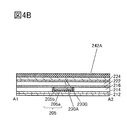
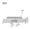
- a conductive film to be a conductor 205a is formed. It is desirable that the conductive film contains a conductor having a function of suppressing the permeation of oxygen.
- a conductor having a function of suppressing the permeation of oxygen For example, tantalum nitride, tungsten nitride, titanium nitride and the like can be used. Alternatively, it can be a laminated film of a conductor having a function of suppressing oxygen permeation and a tantalum, tungsten, titanium, molybdenum, aluminum, copper or molybdenum tungsten alloy.
- the film formation of the conductive film can be performed by using a sputtering method, a CVD method, an MBE method, a PLD method, an ALD method, or the like.
- the conductive film to be the conductor 205a has a multilayer structure.
- tantalum nitride is formed into a film by a sputtering method, and titanium nitride is laminated on the tantalum nitride.
- a metal nitride in the lower layer of the conductor 205b, even if a easily diffusible metal such as copper is used as the conductive film to be the conductor 205b described later, the metal diffuses out from the conductor 205a. Can be prevented.
- a conductive film to be the conductor 205b is formed.
- the film formation of the conductive film can be performed by using a plating method, a sputtering method, a CVD method, an MBE method, a PLD method, an ALD method, or the like.
- a low resistance conductive material such as copper is formed as a conductive film to be the conductor 205b.
- the CMP treatment is performed to remove a part of the conductive film to be the conductor 205a and a part of the conductive film to be the conductor 205b, and expose the insulator 216.
- the conductor 205a and the conductor 205b remain only in the opening.
- the conductor 205 having a flat upper surface can be formed (see FIG. 4).
- a part of the insulator 216 may be removed by the CMP treatment.
- the conductor 205 is formed so as to be embedded in the opening of the insulator 216, but the present embodiment is not limited to this.
- a conductor 205 is formed on the insulator 214, an insulator 216 is formed on the insulator 205, and the insulator 216 is subjected to CMP treatment to remove a part of the insulator 216 and to remove the conductor.
- the surface of 205 may be exposed.
- the insulator 222 is formed on the insulator 216 and the conductor 205.
- an insulator containing an oxide of one or both of aluminum and hafnium may be formed.
- the insulator containing one or both oxides of aluminum and hafnium it is preferable to use aluminum oxide, hafnium oxide, an oxide containing aluminum and hafnium (hafnium aluminate), and the like. Insulators containing oxides of one or both of aluminum and hafnium have barrier properties against oxygen, hydrogen, and water.
- the oxide film 230A and the oxide film 230B are formed on the insulator 224 in this order (see FIG. 4). It is preferable that the oxide film 230A and the oxide film 230B are continuously formed without being exposed to the atmospheric environment. By forming the film without opening it to the atmosphere, it is possible to prevent impurities or moisture from the atmospheric environment from adhering to the oxide film 230A and the oxide film 230B, and the vicinity of the interface between the oxide film 230A and the oxide film 230B can be prevented. Can be kept clean.
- the oxide film 230B is formed by a sputtering method, if the ratio of oxygen contained in the sputtering gas is more than 30% and 100% or less, preferably 70% or more and 100% or less, the oxygen excess type oxidation A physical semiconductor is formed. Transistors using oxygen-rich oxide semiconductors in the channel formation region can obtain relatively high reliability. However, one aspect of the present invention is not limited to this.
- the oxide film 230B is formed by a sputtering method and the ratio of oxygen contained in the sputtering gas is 1% or more and 30% or less, preferably 5% or more and 20% or less, an oxygen-deficient oxide semiconductor is formed. To. A transistor using an oxygen-deficient oxide semiconductor in the channel formation region can obtain a relatively high field-effect mobility. Further, the crystallinity of the oxide film can be improved by forming a film while heating the substrate.
- the resist mask can be removed by performing a dry etching process such as ashing, performing a wet etching process, performing a wet etching process after the dry etching process, or performing a dry etching process after the wet etching process.
- a dry etching process such as ashing, performing a wet etching process, performing a wet etching process after the dry etching process, or performing a dry etching process after the wet etching process.
- the oxide 230a, the oxide 230b, and the conductive layer 242B are formed so that at least a part thereof overlaps with the conductor 205. Further, it is preferable that the side surfaces of the oxide 230a, the oxide 230b, and the conductive layer 242B are substantially perpendicular to the upper surface of the insulator 222. Since the side surfaces of the oxide 230a, the oxide 230b, and the conductive layer 242B are substantially perpendicular to the upper surface of the insulator 222, it is possible to reduce the area and increase the density when a plurality of transistors 200 are provided. Become.
- a curved surface is provided between the side surface of the conductive layer 242B and the upper surface of the conductive layer 242B. That is, it is preferable that the end portion of the side surface and the end portion of the upper surface are curved.
- the curved surface has, for example, a radius of curvature of 3 nm or more and 10 nm or less, preferably 5 nm or more and 6 nm or less at the end of the conductive layer 242B.
- the insulating film is subjected to CMP treatment to form an insulator 280 having a flat upper surface (see FIG. 6).
- the heat treatment may be performed while maintaining the reduced pressure state after the microwave treatment.
- hydrogen in the insulator 280, the oxide 230b, and the oxide 230a can be efficiently removed.
- the heat treatment temperature is preferably 300 ° C. or higher and 500 ° C. or lower.
- the oxide 230b in the region overlapping the opening.
- the amount of film loss in the region corresponds to Lc shown in FIG. 3B.
- the oxide 230b it is preferable to remove a part of the side surface of the oxide 230b in the region overlapping the opening.
- the amount of film loss in the region corresponds to We shown in FIG. 3B.
- a part of the insulator 280, a part of the insulating film 254A, and a part of the conductive layer 242B may be processed under different conditions.
- a part of the insulator 280 may be processed by a dry etching method
- a part of the insulating film 254A may be processed by a wet etching method
- a part of the conductive layer 242B may be processed by a dry etching method.
- a cleaning treatment may be performed in order to remove the above impurities and the like.
- the cleaning method include wet cleaning using a cleaning liquid, plasma treatment using plasma, cleaning by heat treatment, and the like, and the above cleanings may be appropriately combined.
- the cleaning treatment may be performed using an aqueous solution obtained by diluting ammonia water, oxalic acid, phosphoric acid, hydrofluoric acid or the like with carbonated water or pure water, pure water, carbonated water or the like. Further, ultrasonic cleaning may be performed using these aqueous solutions, pure water, or carbonated water. Moreover, you may perform these washings in combination as appropriate.
- the oxide film 230C may be laminated.
- a film may be formed using an oxide target having a [atomic number ratio].
- a part of oxygen contained in the sputtering gas may be supplied to the oxide 230a and the oxide 230b.
- a part of oxygen contained in the sputtering gas may be supplied to the insulator 280. Therefore, the proportion of oxygen contained in the sputtering gas of the oxide film 230C may be 70% or more, preferably 80% or more, and more preferably 100%.
- heat treatment may be performed.
- the heat treatment may be performed under reduced pressure to continuously form the insulating film 250A without exposing it to the atmosphere (see FIG. 8).
- the temperature of the heat treatment is preferably 100 ° C. or higher and 400 ° C. or lower.
- the insulating film 250A can be formed by using a sputtering method, a CVD method, an MBE method, a PLD method, an ALD method, or the like.
- silicon oxide is formed as the insulating film 250A by the CVD method.
- the film forming temperature when forming the insulating film 250A is preferably 350 ° C. or higher and lower than 450 ° C., particularly around 400 ° C. By forming the insulating film 250A at 400 ° C., an insulating film having few impurities can be formed.
- the insulating film as the lower layer of the insulator 250 and the insulating film as the upper layer of the insulator 250 may be continuously formed without being exposed to the atmospheric environment. preferable.
- the film without opening it to the atmosphere it is possible to prevent impurities or moisture from the atmospheric environment from adhering to the insulating film that is the lower layer of the insulator 250 and the insulating film that is the upper layer of the insulator 250.
- the vicinity of the interface between the insulating film that is the lower layer of the insulator 250 and the insulating film that is the upper layer of the insulator 250 can be kept clean.
- microwave treatment may be performed in an atmosphere containing oxygen and under reduced pressure.
- an electric field due to microwaves is applied to the insulating film 250A, the oxide film 230C, the oxide 230b, the oxide 230a, and the like, and V in the oxide film 230C, the oxide 230b, and the oxide 230a.
- the O H can be divided into the V O and hydrogen.
- the hydrogen concentration in the insulating film 250A, the oxide film 230C, the oxide 230b, and the oxide 230a can be reduced. Further, repair or compensate the oxide 230a, in the oxide 230b, and the V O by oxygen is supplied to the V O which may be present after the V O H in the oxide film 230C was divided into the V O and hydrogen can do.
- the conductive film 260A and the conductive film 260B are formed in this order (see FIG. 9).
- the film formation of the conductive film 260A and the conductive film 260B can be performed by using a sputtering method, a CVD method, an MBE method, a PLD method, an ALD method, or the like.
- the conductive film 260A is formed by using the ALD method
- the conductive film 260B is formed by using the CVD method.
- the oxide film 230C, the insulating film 250A, the conductive film 260A, and the conductive film 260B are polished until the insulator 280 is exposed, thereby causing the oxide 230c, the insulator 250, and the conductor 260 (conductive).
- the body 260a and the conductor 260b) are formed (see FIG. 10).
- the oxide 230c is arranged so as to cover the inner wall (side wall and bottom surface) of the opening reaching the oxide 230b.
- the insulator 250 is arranged so as to cover the inner wall of the opening via the oxide 230c.
- the conductor 260 is arranged so as to embed the opening via the oxide 230c and the insulator 250.
- the insulator 282 is formed on the oxide 230c, the insulator 250, the conductor 260, and the insulator 280 (see FIG. 11).
- the film formation of the insulator 282 can be performed by using a sputtering method, a CVD method, an MBE method, a PLD method, an ALD method, or the like.
- oxygen can be added to the insulator 280 while forming the film. At this time, it is preferable to form the insulator 282 while heating the substrate.
- the insulator 282 in contact with the upper surface of the conductor 260, it is possible to suppress the oxygen contained in the insulator 280 from being absorbed by the conductor 260 in the subsequent heat treatment, which is preferable. ..
- heat treatment may be performed.
- the treatment is carried out in a nitrogen atmosphere at a temperature of 400 ° C. for 1 hour.
- oxygen added by the film formation of the insulator 282 can be diffused to the insulator 280, and further supplied to the oxide 230a and the oxide 230b via the oxide 230c.
- the heat treatment is not limited to the film formation of the insulator 283, but may be performed after the film formation of the insulator 282.
- the insulator 274 may be formed on the insulator 283.
- the film formation of the insulator 274 can be performed by using a sputtering method, a CVD method, an MBE method, a PLD method, an ALD method, or the like.
- the insulator 281 may be formed on the insulator 274.
- the film formation of the insulator 281 can be performed by using a sputtering method, a CVD method, an MBE method, a PLD method, an ALD method, or the like.
- an insulating film to be the insulator 241 (insulator 241a and insulator 241b) is formed, and the insulating film is anisotropically etched to form the insulator 241.
- the film formation of the insulating film can be performed by using a sputtering method, a CVD method, an MBE method, a PLD method, an ALD method, or the like.
- the insulating film to be the insulator 241 it is preferable to use an insulating film having a function of suppressing the permeation of oxygen.
- silicon nitride by using the PEALD method. Silicon nitride is preferable because it has a high blocking property against hydrogen.
- the anisotropic etching of the insulating film to be the insulator 241 for example, a dry etching method or the like may be used.
- a dry etching method or the like By providing the insulator 241 on the side wall portion of the opening, it is possible to suppress the permeation of oxygen from the outside and prevent the oxidation of the conductor 240a and the conductor 240b to be formed next. Further, it is possible to prevent impurities such as water and hydrogen from diffusing from the conductor 240a and the conductor 240b to the outside.
- a conductive film to be a conductor 246 is formed.
- the film formation of the conductive film can be performed by using a sputtering method, a CVD method, an MBE method, a PLD method, an ALD method, or the like.
- FIG. 12A shows a top view of the semiconductor device.
- FIG. 12B is a cross-sectional view corresponding to the portion indicated by the alternate long and short dash line of A1-A2 shown in FIG. 12A.
- FIG. 12C is a cross-sectional view corresponding to the portion shown by the alternate long and short dash line of A3-A4 in FIG. 12A.
- FIG. 12D is a cross-sectional view corresponding to the portion shown by the alternate long and short dash line in FIG. 12A of A5-A6.
- FIG. 12A shows a top view of the semiconductor device.
- FIG. 12B is a cross-sectional view corresponding to the portion indicated by the alternate long and short dash line of A1-A2 shown in FIG. 12A.
- FIG. 12C is a cross-sectional view corresponding to the portion shown by the alternate long and short dash line of A3-A4 in FIG. 12A.
- FIG. 12D is a cross-sectional view corresponding to
- the same reference numerals are added to the structures having the same functions as the structures constituting the semiconductor devices shown in ⁇ Semiconductor device configuration example>.
- the constituent material of the semiconductor device the material described in detail in ⁇ Semiconductor device configuration example> can be used.
- the semiconductor device shown in FIG. 12 is a modification of the semiconductor device shown in FIG.
- the semiconductor device shown in FIG. 12 has a different shape of the insulator 283 from the semiconductor device shown in FIG. It also differs in that it has oxides 243 (oxides 243a and oxides 243b). Further, the configuration in which each of the oxide 230c and the insulator 254 is provided as a two-layer laminated structure is shown.
- the insulator 214, the insulator 216, the insulator 222, the insulator 224, the insulator 254, the insulator 280, and the insulator 282 are patterned, and the insulator 283 covers them. It has become. That is, the insulator 283 includes the upper surface and the side surface of the insulator 282, the side surface of the insulator 280, the side surface of the insulator 254, the side surface of the insulator 224, the side surface of the insulator 222, and the side surface of the insulator 216. , In contact with the side surface of the insulator 214 and the upper surface of the insulator 212.
- the insulator 212 and the insulator 283 have a high function of suppressing the diffusion of hydrogen (for example, at least one hydrogen atom, hydrogen molecule, etc.) or water molecule.
- hydrogen for example, at least one hydrogen atom, hydrogen molecule, etc.
- water molecule for example, water molecule.
- the insulator 212 and the insulator 283 it is preferable to use silicon nitride or silicon nitride oxide having a higher hydrogen barrier property.
- the insulator 212, the insulator 214, and the insulator 283 are provided as a single layer, but the present invention is not limited to this.
- the insulator 212, the insulator 214, and the insulator 283 may be provided as a laminated structure of two or more layers.
- the transistor 200 shown in FIG. 12 has an oxide 243 (oxide 243a, which has a function of suppressing oxygen permeation between the conductor 242 (conductor 242a and the conductor 242b) and the oxide 230). And oxide 243b).
- oxide 243a oxide 243 having a function of suppressing the permeation of oxygen between the conductor 242 functioning as a source electrode or a drain electrode and the oxide 230b.
- electricity between the conductor 242 and the oxide 230b can be obtained. This is preferable because the resistance is reduced. With such a configuration, the electrical characteristics of the transistor 200 and the reliability of the transistor 200 can be improved.
- a metal oxide having an element M may be used.
- the element M aluminum, gallium, yttrium, or tin may be used.
- Oxide 243 preferably has a higher concentration of element M than oxide 230b.
- gallium oxide may be used as the oxide 243.
- a metal oxide such as In—M—Zn oxide may be used.
- the atomic number ratio of the element M to In is preferably larger than the atomic number ratio of the element M to In in the metal oxide used for the oxide 230b.
- the film thickness of the oxide 243 is preferably 0.5 nm or more and 5 nm or less, more preferably 1 nm or more and 3 nm or less, and further preferably 1 nm or more and 2 nm or less. Further, the oxide 243 is preferably crystalline. When the oxide 243 has crystallinity, the release of oxygen in the oxide 230 can be suitably suppressed. For example, as the oxide 243, if it has a crystal structure such as a hexagonal crystal, the release of oxygen in the oxide 230 may be suppressed.
- the lower surface of the oxide 230c in the region overlapping the conductor 260 is about the same as the lower surface of the oxide 243 (oxide 243a and oxide 243b), or the oxide. It is preferably lower than the lower surface of 243 (oxides 243a and 243b). With such a shape, impurities near the interface between the oxide 230b and the oxide 230c can be removed, and the low resistance region formed near the upper surface of the region 234 can be reduced.
- the height of the lower surface of the oxide 243 and the height of the lower surface of the oxide 230c in the region overlapping the conductor 260 is 0 nm or more and 10 nm or less, preferably 0 nm or more and 5 nm or less, and more preferably 0 nm or more and 3 nm or less.
- the oxide 230c shows a configuration in which the oxide 230c1 and the oxide 230c2 are laminated.
- the oxide 230c2 preferably contains at least one of the metal elements constituting the metal oxide used in the oxide 230c1, and more preferably contains all the metal elements.
- In-Ga-Zn oxide or In-Zn oxide may be used as the oxide 230c1
- In-Ga-Zn oxide, Ga-Zn oxide, or gallium oxide may be used as the oxide 230c2.
- the defect level density at the interface between the oxide 230c1 and the oxide 230c2 can be lowered.
- the lower end of the conduction band of the oxide 230a and 230c2 is closer to the vacuum level than the lower end of the conduction band of the oxide 230b and the oxide 230c1.
- the electron affinity of the oxide 230a and the oxide 230c2 is preferably smaller than the electron affinity of the oxide 230b and the oxide 230c1.
- the oxide 230c2 uses a metal oxide that can be used for the oxide 230a
- the oxide 230c1 uses a metal oxide that can be used for the oxide 230b.
- the main path of the carrier may be not only the oxide 230b but also the oxide 230c1 as the main path of the carrier.
- the oxide 230c2 is more preferably a metal oxide that suppresses the diffusion or permeation of oxygen than the oxide 230c1.
- oxygen contained in the insulator 280 can be suppressed from diffusing into the insulator 250. Therefore, the oxygen can be efficiently supplied to the oxide 230b via the oxide 230c1.
- the oxide 230c1 may be provided for each transistor 200. That is, the oxide 230c1 of the transistor 200 and the oxide 230c1 of the transistor 200 adjacent to the transistor 200 do not have to be in contact with each other. Further, the oxide 230c1 of the transistor 200 and the oxide 230c1 of the transistor 200 adjacent to the transistor 200 may be separated from each other. In other words, the oxide 230c1 may not be arranged between the transistor 200 and the transistor 200 adjacent to the transistor 200.
- the oxide 230c is independently provided on the transistors 200 by the above configuration. Therefore, it is possible to suppress the occurrence of a parasitic transistor between the transistor 200 and the transistor 200 adjacent to the transistor 200, and to suppress the occurrence of the leak path. Therefore, it is possible to provide a semiconductor device having good electrical characteristics and capable of miniaturization or high integration.
- L 1 is made larger than 0 nm.
- the value of the ratio of L 1 (L 1 / L 2) for L 2 is preferably greater than 0 less than 1, more preferably 0.1 to 0.9, more preferably 0.2 to 0.8 Is.
- L 2 may be the distance between the side ends of the oxide 230b of the transistor 200 facing each other and the side ends of the oxide 230b of the transistor 200 adjacent to the transistor 200.
- oxides 230c1 is a transistor 200, the positional deviation of the arrangement that are not regions between the transistors 200 adjacent to the transistor 200 Even if it occurs, the oxide 230c1 of the transistor 200 and the oxide 230c1 of the transistor 200 adjacent to the transistor 200 can be separated from each other.
- the transistor 200 by increasing the ratio of L 1 to the above L 2 (L 1 / L 2 ), the transistor 200, even by narrowing the interval between the transistor 200 adjacent to the transistor 200, the width of the minimum feature size It can be secured, and the semiconductor device can be further miniaturized or highly integrated.
- the oxide 230c2 has a region in contact with the insulator 224 between the transistor 200 and the transistor 200 adjacent to the transistor 200.
- the oxide 230c2 of the transistor 200 and the oxide 230c2 of the transistor 200 adjacent to the transistor 200 may be separated from each other.
- the insulator 250 has a region in contact with the insulator 224 between the transistor 200 and the transistor 200 adjacent to the transistor 200.
- the insulator 254 shows a configuration in which the insulator 254a and the insulator 254b are laminated.
- the explanations of the lower layer of the insulator 254 and the upper layer of the insulator 254 described in ⁇ Detailed configuration of semiconductor device> can be referred to, respectively.
- the insulator 254 may not be provided, and an insulator functioning as a barrier layer may be provided between the upper surface of the conductor 242 and the insulator 280.
- an insulator functioning as a barrier layer may be provided between the upper surface of the conductor 242 and the insulator 280.
- the insulator has a function of suppressing the diffusion of oxygen.
- the insulator preferably has a function of suppressing the diffusion of oxygen more than the insulator 280.
- an insulator containing an oxide of one or both of aluminum and hafnium may be formed.
- the ALD method By forming by using the ALD method, it is possible to form a film having a dense, reduced defects such as cracks and pinholes, or a uniform thickness.
- an insulator containing aluminum nitride may be used as the insulator.
- [Modification 2 of semiconductor device] 13A and 13B show a configuration in which a plurality of transistors (transistors 200_1 to 200_n) are comprehensively sealed with an insulator 283 and an insulator 212. Note that, in FIGS. 13A and 13B, the transistors 200_1 to 200_n appear to be arranged in the channel length direction, but the transistor 200_1 to the transistor 200_n are not limited to this.
- the transistors 200_1 to 200_n may be arranged in the channel width direction, may be arranged in a matrix, or may be arranged without regularity.
- a portion where the insulator 283 and the insulator 212 are in contact with each other (hereinafter, may be referred to as a sealing portion 265) is formed outside the plurality of transistors (transistors 200_1 to 200_n). ..
- the sealing portion 265 is formed so as to surround the plurality of transistors (also referred to as transistor groups).
- a plurality of transistors can be wrapped with the insulator 283 and the insulator 212. That is, the insulator 283 and the insulator 281 can wrap the side surfaces and the upper side of the plurality of transistors, and the insulator 212 can wrap the lower side thereof. In this way, a plurality of transistor groups surrounded by the sealing portion 265 are provided on the substrate.
- the distance between the sealing portion 265 and the oxide 230 closest to the sealing portion 265 is short.
- the distance between the sealing portion 265 and the oxide 230 closest to the sealing portion 265 is preferably 1 ⁇ m or less, more preferably 500 nm or less.
- a dicing line (sometimes referred to as a scribe line, a dividing line, or a cutting line) may be provided on the sealing portion 265. Since the substrate is divided at the dicing line, the transistor group surrounded by the sealing portion 265 is taken out as one chip.
- FIG. 13A shows an example in which a plurality of transistors (transistors 200_1 to 200_n) are surrounded by one sealing portion 265, but the present invention is not limited to this.
- a plurality of transistors may be surrounded by a plurality of sealing portions.
- the plurality of transistors are surrounded by the sealing portion 265a, and further surrounded by the outer sealing portion 265b.
- the portion where the insulator 283 and the insulator 212 are in contact with each other increases, so that the adhesion between the insulator 283 and the insulator 212 can be further improved. Can be done. As a result, the plurality of transistors can be more reliably sealed.
- a dicing line may be provided on the sealing portion 265a or the sealing portion 265b, or a dicing line may be provided between the sealing portion 265a and the sealing portion 265b.
- the insulator 212 shows a configuration in which a lower layer of the insulator 212 and an upper layer of the insulator 212 are laminated.
- silicon nitride is formed as a lower layer of the insulator 212 by a PECVD method
- silicon nitride is formed as an upper layer of the insulator 212 by a sputtering method.
- the lower layer of the insulator 212 can be formed at a higher rate than the upper layer of the insulator 212, so that the productivity can be improved.
- the hydrogen concentration in the upper layer of the insulator 212 arranged closer to the oxide 230 than the lower layer of the insulator 212 can be reduced as compared with the lower layer of the insulator 212.
- an insulator such as silicon nitride, which is difficult for impurities such as water and hydrogen to permeate, as the insulator 212, impurities such as water and hydrogen are diffused from the layer below the insulator 212 (not shown). Can be suppressed.
- the metal can be used as the insulator 212. It can be suppressed from spreading upward through.
- the structure is not limited to the above, and a single-layer structure may be provided in which either the lower layer of the insulator 212 or the upper layer of the insulator 212 is provided. Further, although the structure is such that the insulator 214 is provided in FIGS. 13 and (B), the structure is not limited to this, and the structure may not include the insulator 214.
- a semiconductor device having little variation in transistor characteristics it is possible to provide a semiconductor device having a large on-current. Further, according to one aspect of the present invention, it is possible to provide a semiconductor device having good electrical characteristics. Further, according to one aspect of the present invention, it is possible to provide a semiconductor device capable of miniaturization or high integration. Further, according to one aspect of the present invention, it is possible to provide a semiconductor device having good reliability. Further, according to one aspect of the present invention, a semiconductor device having low power consumption can be provided.
- FIG. 14 shows an example of a semiconductor device (storage device) which is one aspect of the present invention.
- the transistor 200 is provided above the transistor 300, and the capacitive element 100 is provided above the transistor 300 and the transistor 200.
- the transistor 200 the transistor 200 described in the previous embodiment can be used. Therefore, for the transistor 200 and the layer including the transistor 200, the description of the previous embodiment can be taken into consideration.
- the wiring 1001 is electrically connected to the source of the transistor 300, and the wiring 1002 is electrically connected to the drain of the transistor 300. Further, the wiring 1003 is electrically connected to one of the source and drain of the transistor 200, the wiring 1004 is electrically connected to the first gate of the transistor 200, and the wiring 1006 is electrically connected to the second gate of the transistor 200. It is connected to the. The gate of the transistor 300 and the other of the source and drain of the transistor 200 are electrically connected to one of the electrodes of the capacitive element 100, and the wiring 1005 is electrically connected to the other of the electrodes of the capacitive element 100. ..
- the storage devices shown in FIG. 14 can form a memory cell array by arranging them in a matrix.
- the transistor 300 is provided on the substrate 311 and functions as a conductor 316 that functions as a gate, an insulator 315 that functions as a gate insulator, a semiconductor region 313 that is a part of the substrate 311 and a low that functions as a source region or a drain region. It has a resistance region 314a and a low resistance region 314b.
- the transistor 300 may be either a p-channel type or an n-channel type.
- the semiconductor region 313 (a part of the substrate 311) on which the channel is formed has a convex shape. Further, the side surface and the upper surface of the semiconductor region 313 are provided so as to be covered with the conductor 316 via the insulator 315.
- the conductor 316 may be made of a material that adjusts the work function. Since such a transistor 300 utilizes a convex portion of a semiconductor substrate, it is also called a FIN type transistor. It should be noted that an insulator that is in contact with the upper portion of the convex portion and functions as a mask for forming the convex portion may be provided. Further, although the case where a part of the semiconductor substrate is processed to form a convex portion is shown here, the SOI substrate may be processed to form a semiconductor film having a convex shape.
- the transistor 300 shown in FIG. 14 is an example, and the transistor 300 is not limited to the structure thereof, and an appropriate transistor may be used according to the circuit configuration and the driving method.
- the capacitive element 100 is provided above the transistor 200.
- the capacitive element 100 has a conductor 110 that functions as a first electrode, a conductor 120 that functions as a second electrode, and an insulator 130 that functions as a dielectric.
- the conductor 112 provided on the conductor 240 and the conductor 110 can be formed at the same time.
- the conductor 112 has a function as a plug or wiring that electrically connects to the capacitance element 100, the transistor 200, or the transistor 300.
- the conductor 112 and the conductor 110 have a single-layer structure, but the structure is not limited to this, and a laminated structure of two or more layers may be used.
- a conductor having a barrier property and a conductor having a high adhesion to a conductor having a high conductivity may be formed between a conductor having a barrier property and a conductor having a high conductivity.
- the insulator 130 includes, for example, silicon oxide, silicon nitride, silicon nitride, silicon nitride, aluminum oxide, aluminum nitride, aluminum nitride, aluminum nitride, hafnium oxide, hafnium oxide, hafnium nitride, hafnium nitride. Etc. may be used, and it can be provided in a laminated or single layer.
- the capacitance element 100 can secure a sufficient capacitance by having an insulator having a high dielectric constant (high-k), and by having an insulator having a large dielectric strength, the dielectric strength is improved and the capacitance is improved.
- the electrostatic breakdown of the element 100 can be suppressed.
- the insulator of the high dielectric constant (high-k) material material having a high specific dielectric constant
- the insulator that functions as an interlayer film may function as a flattening film that covers the uneven shape below the insulator.
- the upper surface of the insulator 322 may be flattened by a flattening treatment using a chemical mechanical polishing (CMP) method or the like in order to improve the flatness.
- CMP chemical mechanical polishing
- the motherboard 1203 may be provided with a storage device such as a DRAM 1221 and a flash memory 1222.
- a storage device such as a DRAM 1221 and a flash memory 1222.
- the DOSRAM shown in the previous embodiment can be used for the DRAM 1221.
- the NO SRAM shown in the above embodiment can be used for the flash memory 1222.
- FIG. 20A is a schematic view of the USB memory.
- the USB memory 1100 has a housing 1101, a cap 1102, a USB connector 1103, and a board 1104.
- the substrate 1104 is housed in the housing 1101.
- a memory chip 1105 and a controller chip 1106 are attached to the substrate 1104.
- the semiconductor device shown in the previous embodiment can be incorporated into the memory chip 1105 or the like.
- FIG. 21A illustrates a mobile phone (smartphone) which is a kind of information terminal.
- the information terminal 5100 has a housing 5101 and a display unit 5102, and as an input interface, a touch panel is provided in the display unit 5102 and buttons are provided in the housing 5101.
- FIG. 21B illustrates a notebook information terminal 5200.
- the notebook-type information terminal 5200 includes a main body 5201 of the information terminal, a display unit 5202, and a keyboard 5203.
- a smartphone and a notebook-type information terminal are taken as examples of electronic devices, which are shown in FIGS. 21A and 21B, respectively, but information terminals other than the smartphone and the notebook-type information terminal can be applied.
- information terminals other than smartphones and notebook-type information terminals include PDAs (Personal Digital Assistants), desktop-type information terminals, workstations, and the like.
- the GPU or chip of one aspect of the present invention can be applied to a large computer.
- the supercomputer 5500 has a rack 5501 and a plurality of rack-mounted computers 5502.
- the plurality of computers 5502 are stored in the rack 5501. Further, the computer 5502 is provided with a plurality of substrates 5504, and the GPU or chip described in the above embodiment can be mounted on the substrate.
- the GPU or chip of one aspect of the present invention can be applied to a moving vehicle and around the driver's seat of the vehicle.
- FIG. 21G is a diagram showing the periphery of the windshield in the interior of an automobile, which is an example of a moving body.
- a display panel 5701 attached to the dashboard a display panel 5702, a display panel 5703, and a display panel 5704 attached to the pillar are shown.
- the display panel 5701 to the display panel 5703 can provide various other information by displaying a speedometer, a tachometer, a mileage, a fuel gauge, a gear state, an air conditioner setting, and the like.
- the display items and layout displayed on the display panel can be appropriately changed according to the user's preference, and the design can be improved.
- the display panel 5701 to 5703 can also be used as a lighting device.
- electric refrigerators and freezers have been described as an example of electric appliances
- other electric appliances include, for example, vacuum cleaners, microwave ovens, microwave ovens, rice cookers, water heaters, IH cookers, water servers, air conditioners and air conditioners. Examples include washing machines, dryers, and audiovisual equipment.
- a transistor 800 having a structure equivalent to that of the transistor 200 disclosed in the above embodiment was manufactured.
- the channel length and channel width were set to 60 nm, respectively, and the thickness of the gate insulating layer (TGI) was set to 6 nm in terms of EOT (Equivalent Oxide Pickness).
- TGI gate insulating layer
- CAAC-IGZO was used for the semiconductor layer in which a channel is formed.
- the transistor 800 is a field effect transistor (also referred to as "CAAC-IGZO FET") using CAAC-IGZO in the semiconductor layer.
- FIG. 22A and 22B show cross-sectional TEM photographs of the transistor 800.
- FIG. 22A is a cross-sectional TEM photograph of the transistor 800 in the gate length direction
- FIG. 22B is a cross-sectional TEM photograph of the transistor 800 in the gate width direction.
- 22A and 22B show the gate electrode (TGE), gate insulating layer (TGI), source electrode and drain electrode (SDE), semiconductor layer (CAAC-IGZO), back gate insulating layer (BGI), and the back gate insulating layer (BGI) of the transistor 800.
- a backgate electrode (BGE) is shown. Since FIG. 22B is a cross-sectional TEM photograph in the gate width direction passing through the gate electrode and the back gate electrode, the SDE is not shown.
- the Id-Vg characteristic of the transistor 800 was measured. Specifically, the voltage between the source and drain of the transistor 800 (also referred to as “drain voltage” or “Vds”) is set to 1.3V, and the voltage supplied to the back gate (also referred to as “Vbg”) is set to 0V. Then, the current (also referred to as “drain current” or “Id”) flowing between the source and the drain when the gate voltage (also referred to as "Vg”) was changed from -3V to 3V was measured. The Id-Vg characteristics were measured at four temperatures of ⁇ 40 ° C., room temperature (27 ° C.), 85 ° C., and 125 ° C.
- FIG. 23 shows the measurement results of the Id-Vg characteristic of the transistor 800.
- the horizontal axis of FIG. 23 is Vg, and the vertical axis shows Id on a log scale.
- the lower limit of measurement (ML) of the measuring instrument is 1 ⁇ 10 -13 A. ML is shown by a broken line in FIG. 23.
- the threshold voltage of the transistor M1 can be changed by the voltage (Vbg1) supplied to the terminal bg1.
- the threshold voltage of the transistor M2 can be changed by the voltage (Vbg2) supplied to the terminal bg2.
- the logic threshold value of the inverter circuit 810 can be adjusted by changing the voltage supplied to the back gate.
- FIG. 26A shows a circuit diagram of the ring oscillator 820.
- the ring oscillator 820 is composed of a core 811 and an output buffer 812.
- the core 811 has an odd-numbered stage inverter circuit 810 connected in a ring shape.
- the first stage inverter circuit 810 is referred to as an inverter circuit 810_1
- the second stage inverter circuit 810 is referred to as an inverter circuit 810_2
- the nth stage inverter circuit 810 is referred to as an inverter circuit 810_n (n is an odd number of 3 or more). .) Is shown.
- the output of the inverter circuit 810 of the i-th stage (i is a natural number of 2 or more and n-1 or less) is electrically connected to the input of the inverter circuit 810 of the i + 1 stage. Further, the output of the inverter circuit 810 of the i-1st stage is electrically connected to the input of the inverter circuit 810 of the i-1st stage. Further, the output of the nth stage inverter circuit 810 is electrically connected to the input of the first stage inverter circuit 810. In the core 811 the inverter circuit 810 is connected in an annular shape.
- the input of the output buffer 812 is electrically connected to the output of any inverter circuit 810 among the odd number of inverter circuits 810 included in the core 811.
- the output of the i-stage inverter circuit 810 is electrically connected to the input of the output buffer 812.
- the output of the output buffer 812 is electrically connected to the terminal Rout.
- a ring oscillator 820 having a core 811 having a 151-stage inverter circuit 810 was manufactured.
- FIG. 26B shows a die photograph of the produced ring oscillator 820.
- the size of the core 811 is 100 ⁇ m ⁇ 350 ⁇ m.
- the delay time changes with the operating temperature. However, by adjusting Vbg2, the delay time can be adjusted to the same time as when operating at room temperature even in a high temperature environment.
- FIG. 28 shows the temperature dependence of the delay time, which is standardized by the delay time at room temperature.
- FIG. 28 shows the delay time when the operating temperature is room temperature (RT: 27 ° C.), 85 ° C., 125 ° C., and 150 ° C. Further, the horizontal axis of FIG. 28 indicates the temperature, and the vertical axis on the left side indicates the delay time specified by the delay time at room temperature as a percentage. The vertical axis on the right side shows the value of Vbg2.
- the delay time measurement at room temperature was performed with Vbg1 set to 0V and Vbg2 set to 2V.
- X shown in FIG. 28 indicates the result of measuring the delay time with Vbg2 set to 2V at all operating temperatures. It can be seen that the delay time becomes shorter as the operating temperature rises. At an operating temperature of 150 ° C., the delay time is about 35% shorter than that at room temperature. This is because the temperature causes a decrease in the threshold voltage and an increase in the field effect mobility.
- “ ⁇ ” shown in FIG. 28 indicates the result of measuring the delay time by adjusting Vbg2 according to the operating temperature.
- “ ⁇ ” shown in FIG. 28 indicates the value of Vbg2 set for each operating temperature.
- “ ⁇ ” shown in FIG. 28 indicates the delay time calculation result of the CMOS inverter using the SPICE simulation.
- the transistor constituting the CMOS inverter a general bulk Si transistor having a channel length of 60 nm is assumed. From FIG. 28, it can be seen that in the CMOS inverter, the delay time becomes longer as the operating temperature rises. At an operating temperature of 150 ° C., the delay time is about 14% longer than that at room temperature. This is because the temperature rise causes the threshold voltage to rise and the field effect mobility to decrease. It is difficult to provide a back gate with a general bulk Si transistor. Therefore, it is difficult to adjust the delay time for each operating temperature.
- CAAC-IGZO FET By using the CAAC-IGZO FET, it is possible to increase the operating speed by increasing the temperature and to keep the speed constant by a simple correction circuit.
Landscapes
- Thin Film Transistor (AREA)
- Metal-Oxide And Bipolar Metal-Oxide Semiconductor Integrated Circuits (AREA)
- Semiconductor Memories (AREA)
- Non-Volatile Memory (AREA)
Priority Applications (7)
| Application Number | Priority Date | Filing Date | Title |
|---|---|---|---|
| US17/606,533 US20220208794A1 (en) | 2019-05-08 | 2020-04-27 | Semiconductor device |
| CN202080032977.5A CN113767479A (zh) | 2019-05-08 | 2020-04-27 | 半导体装置 |
| KR1020217037201A KR20220006071A (ko) | 2019-05-08 | 2020-04-27 | 반도체 장치 |
| JP2021518220A JP7530888B2 (ja) | 2019-05-08 | 2020-04-27 | 半導体装置 |
| JP2024121902A JP7746479B2 (ja) | 2019-05-08 | 2024-07-29 | 半導体装置 |
| US19/169,056 US20250261448A1 (en) | 2019-05-08 | 2025-04-03 | Semiconductor device |
| JP2025153783A JP2026001010A (ja) | 2019-05-08 | 2025-09-17 | 半導体装置 |
Applications Claiming Priority (2)
| Application Number | Priority Date | Filing Date | Title |
|---|---|---|---|
| JP2019-088132 | 2019-05-08 | ||
| JP2019088132 | 2019-05-08 |
Related Child Applications (2)
| Application Number | Title | Priority Date | Filing Date |
|---|---|---|---|
| US17/606,533 A-371-Of-International US20220208794A1 (en) | 2019-05-08 | 2020-04-27 | Semiconductor device |
| US19/169,056 Continuation US20250261448A1 (en) | 2019-05-08 | 2025-04-03 | Semiconductor device |
Publications (1)
| Publication Number | Publication Date |
|---|---|
| WO2020225641A1 true WO2020225641A1 (ja) | 2020-11-12 |
Family
ID=73051034
Family Applications (1)
| Application Number | Title | Priority Date | Filing Date |
|---|---|---|---|
| PCT/IB2020/053916 Ceased WO2020225641A1 (ja) | 2019-05-08 | 2020-04-27 | 半導体装置 |
Country Status (5)
| Country | Link |
|---|---|
| US (2) | US20220208794A1 (enExample) |
| JP (3) | JP7530888B2 (enExample) |
| KR (1) | KR20220006071A (enExample) |
| CN (1) | CN113767479A (enExample) |
| WO (1) | WO2020225641A1 (enExample) |
Families Citing this family (1)
| Publication number | Priority date | Publication date | Assignee | Title |
|---|---|---|---|---|
| JP7352058B2 (ja) * | 2017-11-01 | 2023-09-28 | セントラル硝子株式会社 | 炭化ケイ素単結晶の製造方法 |
Citations (3)
| Publication number | Priority date | Publication date | Assignee | Title |
|---|---|---|---|---|
| JP2015079949A (ja) * | 2013-09-13 | 2015-04-23 | 株式会社半導体エネルギー研究所 | トランジスタ、クロックドインバータ回路、順序回路、および順序回路を備えた半導体装置 |
| JP2016032297A (ja) * | 2014-07-25 | 2016-03-07 | 株式会社半導体エネルギー研究所 | 発振回路、および、それを有する半導体装置 |
| US20180246160A1 (en) * | 2017-02-24 | 2018-08-30 | Semiconductor Manufacturing International (Shanghai) Corporation | Detection method and detection device of process corner of mos transistor |
Family Cites Families (7)
| Publication number | Priority date | Publication date | Assignee | Title |
|---|---|---|---|---|
| US4985643A (en) * | 1988-06-24 | 1991-01-15 | National Semiconductor Corporation | Speed enhancement technique for CMOS circuits |
| WO2011103558A1 (en) | 2010-02-22 | 2011-08-25 | Nantero, Inc. | Logic elements comprising carbon nanotube field effect transistor (cntfet) devices and methods of making same |
| US20130207102A1 (en) | 2012-02-15 | 2013-08-15 | Semiconductor Energy Laboratory Co., Ltd. | Semiconductor device |
| US8988152B2 (en) | 2012-02-29 | 2015-03-24 | Semiconductor Energy Laboratory Co., Ltd. | Semiconductor device |
| JP2016019235A (ja) * | 2014-07-10 | 2016-02-01 | 株式会社半導体理工学研究センター | 増幅回路、cmosインバータ増幅回路、比較回路、δςアナログデジタル変換器、及び半導体装置 |
| US10038402B2 (en) | 2015-10-30 | 2018-07-31 | Semiconductor Energy Laboratory Co., Ltd. | Semiconductor device and electronic device |
| JP2018101884A (ja) | 2016-12-20 | 2018-06-28 | 株式会社半導体エネルギー研究所 | 映像再生装置、その動作方法および電子機器 |
-
2020
- 2020-04-27 US US17/606,533 patent/US20220208794A1/en not_active Abandoned
- 2020-04-27 JP JP2021518220A patent/JP7530888B2/ja active Active
- 2020-04-27 CN CN202080032977.5A patent/CN113767479A/zh active Pending
- 2020-04-27 KR KR1020217037201A patent/KR20220006071A/ko active Pending
- 2020-04-27 WO PCT/IB2020/053916 patent/WO2020225641A1/ja not_active Ceased
-
2024
- 2024-07-29 JP JP2024121902A patent/JP7746479B2/ja active Active
-
2025
- 2025-04-03 US US19/169,056 patent/US20250261448A1/en active Pending
- 2025-09-17 JP JP2025153783A patent/JP2026001010A/ja active Pending
Patent Citations (3)
| Publication number | Priority date | Publication date | Assignee | Title |
|---|---|---|---|---|
| JP2015079949A (ja) * | 2013-09-13 | 2015-04-23 | 株式会社半導体エネルギー研究所 | トランジスタ、クロックドインバータ回路、順序回路、および順序回路を備えた半導体装置 |
| JP2016032297A (ja) * | 2014-07-25 | 2016-03-07 | 株式会社半導体エネルギー研究所 | 発振回路、および、それを有する半導体装置 |
| US20180246160A1 (en) * | 2017-02-24 | 2018-08-30 | Semiconductor Manufacturing International (Shanghai) Corporation | Detection method and detection device of process corner of mos transistor |
Also Published As
| Publication number | Publication date |
|---|---|
| JP2026001010A (ja) | 2026-01-06 |
| US20220208794A1 (en) | 2022-06-30 |
| JP7746479B2 (ja) | 2025-09-30 |
| JP7530888B2 (ja) | 2024-08-08 |
| US20250261448A1 (en) | 2025-08-14 |
| JP2024149532A (ja) | 2024-10-18 |
| JPWO2020225641A1 (enExample) | 2020-11-12 |
| KR20220006071A (ko) | 2022-01-14 |
| CN113767479A (zh) | 2021-12-07 |
Similar Documents
| Publication | Publication Date | Title |
|---|---|---|
| US12063798B2 (en) | Semiconductor device and method for manufacturing semiconductor device | |
| WO2021053473A1 (ja) | 半導体装置、および半導体装置の作製方法 | |
| JPWO2020003047A1 (ja) | 半導体装置、および半導体装置の作製方法 | |
| JP7229669B2 (ja) | 半導体装置、および半導体装置の作製方法 | |
| US20210126130A1 (en) | Semiconductor device and method for manufacturing semiconductor device | |
| JP7508374B2 (ja) | 半導体装置 | |
| JPWO2019111096A1 (ja) | 半導体装置、および半導体装置の作製方法 | |
| WO2019166906A1 (ja) | 半導体装置、および半導体装置の作製方法 | |
| JP7170671B2 (ja) | 半導体装置 | |
| JPWO2020008296A1 (ja) | 半導体装置、および半導体装置の作製方法 | |
| JPWO2020074999A1 (ja) | 半導体装置、および半導体装置の作製方法 | |
| JPWO2020084415A1 (ja) | 半導体装置、および半導体装置の作製方法 | |
| WO2020201870A1 (ja) | 半導体装置、および半導体装置の作製方法 | |
| JPWO2020115595A1 (ja) | 半導体装置、および半導体装置の作製方法 | |
| JPWO2019207429A1 (ja) | 半導体装置、および半導体装置の作製方法 | |
| JPWO2019197946A1 (ja) | 半導体装置、および半導体装置の作製方法 | |
| JPWO2019162807A1 (ja) | 半導体装置、および半導体装置の作製方法 | |
| JP2026001010A (ja) | 半導体装置 | |
| WO2021191716A1 (ja) | 半導体装置及び半導体装置の作製方法 | |
| JPWO2020049420A1 (ja) | 半導体装置、および半導体装置の作製方法 | |
| JPWO2019145807A1 (ja) | 半導体装置、および半導体装置の作製方法 | |
| JPWO2020053697A1 (ja) | 半導体装置、および半導体装置の作製方法 | |
| JPWO2019166914A1 (ja) | 半導体装置、および半導体装置の作製方法 | |
| JP7314249B2 (ja) | 半導体装置 | |
| WO2020201873A1 (ja) | 半導体装置の作製方法 |
Legal Events
| Date | Code | Title | Description |
|---|---|---|---|
| 121 | Ep: the epo has been informed by wipo that ep was designated in this application |
Ref document number: 20802404 Country of ref document: EP Kind code of ref document: A1 |
|
| ENP | Entry into the national phase |
Ref document number: 2021518220 Country of ref document: JP Kind code of ref document: A |
|
| NENP | Non-entry into the national phase |
Ref country code: DE |
|
| ENP | Entry into the national phase |
Ref document number: 20217037201 Country of ref document: KR Kind code of ref document: A |
|
| 122 | Ep: pct application non-entry in european phase |
Ref document number: 20802404 Country of ref document: EP Kind code of ref document: A1 |