WO2020217837A1 - 電流センサ - Google Patents
電流センサ Download PDFInfo
- Publication number
- WO2020217837A1 WO2020217837A1 PCT/JP2020/013545 JP2020013545W WO2020217837A1 WO 2020217837 A1 WO2020217837 A1 WO 2020217837A1 JP 2020013545 W JP2020013545 W JP 2020013545W WO 2020217837 A1 WO2020217837 A1 WO 2020217837A1
- Authority
- WO
- WIPO (PCT)
- Prior art keywords
- core
- housing
- current sensor
- split
- pair
- Prior art date
Links
Images


Classifications
-
- G—PHYSICS
- G01—MEASURING; TESTING
- G01R—MEASURING ELECTRIC VARIABLES; MEASURING MAGNETIC VARIABLES
- G01R15/00—Details of measuring arrangements of the types provided for in groups G01R17/00 - G01R29/00, G01R33/00 - G01R33/26 or G01R35/00
- G01R15/14—Adaptations providing voltage or current isolation, e.g. for high-voltage or high-current networks
- G01R15/18—Adaptations providing voltage or current isolation, e.g. for high-voltage or high-current networks using inductive devices, e.g. transformers
- G01R15/186—Adaptations providing voltage or current isolation, e.g. for high-voltage or high-current networks using inductive devices, e.g. transformers using current transformers with a core consisting of two or more parts, e.g. clamp-on type
-
- G—PHYSICS
- G01—MEASURING; TESTING
- G01R—MEASURING ELECTRIC VARIABLES; MEASURING MAGNETIC VARIABLES
- G01R19/00—Arrangements for measuring currents or voltages or for indicating presence or sign thereof
- G01R19/145—Indicating the presence of current or voltage
- G01R19/15—Indicating the presence of current
Definitions
- This disclosure relates to a current sensor.
- Patent Document 1 discloses a conventional current sensor in which an electric conductor is arranged so as to penetrate an annular core in which a coil is partially wound.
- the annular core is divided in order to facilitate the arrangement of the electric conductor in the annular core.
- the electric conductor is first arranged in the divided core, and then the core is assembled so that the electric conductor penetrates into the annular core.
- the current sensor detects the current flowing through the electric conductor.
- the current sensor comprises a core having a hollow portion configured to penetrate an electrical conductor and a coil wound around the core.
- the core has substantially a C-shape with a gap leading to the hollow portion.
- the core has a pair of end faces facing each other in opposite directions through a gap.
- the core has a plurality of split cores joined to each other. Each pair of split cores adjacent to each other among the plurality of split cores has a joint surface parallel to each other in the opposite direction.
- This current sensor can achieve the desired sensitivity characteristics.
- FIG. 1 is a perspective view of the current sensor according to the embodiment.
- FIG. 2 is an exploded perspective view of the current sensor according to the embodiment.
- FIG. 3 is a cross-sectional view taken along the line III-III of the current sensor shown in FIG.
- FIG. 4 is a perspective view of the sensor unit of the current sensor according to the embodiment.
- FIG. 5 is an exploded perspective view of the sensor unit according to the embodiment.
- FIG. 6 is a plan view of the sensor unit according to the embodiment.
- FIG. 7 is a graph showing a BH curve of ferrite, which is a core material according to the embodiment.
- FIG. 8 is an explanatory diagram comparing the output waveforms of the core according to the embodiment and the core of the comparative example.
- FIG. 1 is a perspective view of the current sensor according to the embodiment.
- FIG. 2 is an exploded perspective view of the current sensor according to the embodiment.
- FIG. 3 is a cross-sectional view taken along the line III-III of the current
- FIG. 9 is a graph showing the relationship between the gap between the cores of the current sensor and the output according to the embodiment.
- FIG. 10A is a front view of another core according to the embodiment.
- FIG. 10B is a side view of the core shown in FIG. 10A.
- FIG. 11 is a graph showing the current and output in the core according to the embodiment.
- FIG. 12 is a plan view of still another core according to the embodiment.
- FIG. 13 is a plan view of still another core according to the embodiment.
- FIG. 14A is an explanatory diagram showing the influence of the electric conductor of the core of the modified example 1.
- FIG. 14B is an explanatory diagram showing the influence of the electric conductor of the core of the modified example 2.
- FIG. 14A is an explanatory diagram showing the influence of the electric conductor of the core of the modified example 1.
- FIG. 14B is an explanatory diagram showing the influence of the electric conductor of the core of the modified example 2.
- FIG. 14C is an explanatory diagram showing the influence of the electric conductor of the core according to the embodiment.
- FIG. 15 is an explanatory diagram showing a core and an output of the current sensor according to the embodiment.
- FIG. 16 is an explanatory diagram showing a core and an output graph of the current sensor according to the embodiment.
- FIG. 17 is an explanatory diagram showing a core and an output of the current sensor according to the embodiment.
- FIG. 18 is a perspective view of another current sensor according to the embodiment.
- FIG. 19 is a cross-sectional view taken along the line XIX-XIX of the current sensor shown in FIG.
- FIG. 20 is a cross-sectional view taken along the line XX-XX of the current sensor shown in FIG. FIG.
- FIG. 21 is a perspective view of the housing of the current sensor shown in FIG.
- FIG. 22 is an enlarged cross-sectional view of the current sensor shown in FIG.
- FIG. 23 is a perspective view of the sensor unit of the current sensor shown in FIG.
- FIG. 24 is a perspective view of another sensor unit of the current sensor shown in FIG.
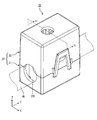
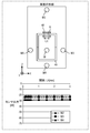
- FIG. 1 is a perspective view showing a schematic configuration of the current sensor 10 according to the embodiment.
- FIG. 2 is an exploded perspective view of the current sensor 10.
- FIG. 3 is a cross-sectional view taken along the line III-III of the current sensor 10 shown in FIG.
- the wire-shaped electric conductor W to be detected is shown by a broken line.
- the X-axis direction may be referred to as the width direction X
- the Y-axis direction may be referred to as the thickness direction Y
- the Z-axis direction may be referred to as the vertical direction Z.
- the current sensor 10 is a Current Transformer (CT) type current sensor that detects an alternating current flowing through the electric conductor W.
- CT Current Transformer
- the current sensor 10 includes a housing 20 and a sensor unit 30 housed in the housing 20.
- the housing 20 is formed in a substantially rectangular parallelepiped shape as a whole with, for example, a non-magnetic resin.
- the thickness (length in the Y-axis direction) of the housing 20 is constant as a whole.
- the housing 20 is divided into two housings 21 and 22 in the Z-axis direction. The portion in the negative direction of the Z-axis is the housing 21, and the portion in the positive direction of the Z-axis is the housing 22. is there.
- the housing 21 includes a box-shaped main body portion 211 having a space 21s in which the positive direction of the Z axis is open, and a pair of locking portions 212 that are locked to the housing 22.
- the main body portion 211 has a pair of lower wall portions 213 facing each other in the Y-axis direction, a pair of lower wall portions 214 facing each other in the X-axis direction, and a bottom plate portion 219.
- the lower wall portions 213 and 214 are connected to each other and extend from the bottom plate portion 219 to the plus side of the Z axis.
- the lower wall portions 213 and 214 and the bottom plate portion 219 surround the space 21s. Further, inside the housing 21, a pair of inner wall portions 215 parallel to the lower wall portion 213 are provided.
- the pair of inner wall portions 215 are arranged at predetermined intervals in the Y-axis direction. A part of the sensor unit 30 is fitted and fixed between the pair of inner wall portions 215. Further, the pair of lower wall portions 213 are formed with a notch portion 213a having a semicircular arc shape, and the pair of inner wall portions 215 are formed with a semicircular notch portion 215a.
- the pair of locking portions 212 extend from the outer surface of the pair of lower wall portions 214 in the positive direction of the Z axis.
- the pair of locking portions 212 have a substantially U-shape.
- Each of the pair of locking portions 212 engages with a plurality of engaging protrusions 228a and 228b of the housing 22 to integrally fix the housing 21 and the housing 22 to each other.
- the housing 22 has a box shape having a space 22s in which the negative direction of the Z axis is open.
- the housing 22 has a pair of upper wall portions 223 facing each other in the Y-axis direction, a pair of upper wall portions 224 facing each other in the X-axis direction, and a floor plate portion 229.
- the upper wall portions 223 and 224 are connected to each other and extend from the bottom plate portion 229 to the minus side of the Z axis.
- the upper wall portion 223 and 224 and the bottom plate portion 229 surround the space 22s.
- a semicircular notch 223a is formed in each of the pair of upper wall portions 223.
- the notch 223a forms the through hole 20h shown in FIG. 1 together with the notch 213a of the housing 21 when the housing 21 and the housing 22 are assembled.
- the electric conductor W is inserted into the through hole 20h. In this state, the electric conductor W is also housed in the notch 215a of the pair of inner wall portions 215 of the housing 21.
- the notch portions 213a, 215a, and 223a also function as support portions for supporting the electric conductor W.
- a pair of protrusions 224a that sandwich the sensor unit 30 in the Y-axis direction are formed on the inner surface of the pair of upper wall portions 224.
- FIG. 3 of the pair of protrusions 224a only the protrusion 224a in the positive direction of the Y-axis is shown.
- the pair of protrusions 224a extend in the Z-axis direction.
- the pair of protrusions 224a are arranged at predetermined intervals in the Y-axis direction. A part of the sensor unit 30 is fitted and fixed between the pair of protrusions 224a.
- regulation convex portions 224b that regulate the vertical displacement of the sensor unit 30 are provided.
- the regulation convex portion 224b is arranged between the pair of protrusions 224a and extends in the Z-axis direction.
- the lower end surface of the regulation convex portion 224b comes into contact with the upper end surface of the sensor unit 30 to regulate the displacement of the sensor unit 30 with respect to the housing 20 in the vertical direction Z.
- Three engaging protrusions 228a and 228b are provided on the outer surfaces of the pair of upper wall portions 224.
- the two engaging protrusions 228b are provided at the lower ends of the upper wall portion 224 and are arranged at predetermined intervals in the Y-axis direction.
- the two engaging protrusions 228b sandwich the locking portion 212 of the housing 21 in the Y-axis direction.
- the remaining one engaging protrusion 228a is arranged above the center of the two engaging protrusions 228b in the Y-axis direction.
- the engaging projection 228b supports the upper portion of the locking portion 212 of the housing 21 from below.
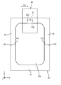
- FIG. 4 is a perspective view showing a schematic configuration of the sensor unit 30 according to the embodiment.
- FIG. 5 is an exploded perspective view of the sensor unit 30 according to the embodiment.
- FIG. 6 is a plan view of the sensor unit 30 according to the embodiment.
- the sensor unit 30 includes a core 40, a bobbin 50, and a coil 60.
- the core 40 is made of a magnetic material such as ferrite, and has a substantially C-shape having a hollow portion 40h and a gap S connected to the hollow portion 40h.
- the core 40 has a rectangular frame shape in a plan view.
- the gap S is provided in the center of the upper frame portion of the rectangular frame shape.
- the cross sections of the four outer corners of the core 40 are corners with sharp tips, and the cross sections of the four inner corners are arcuate corners.
- the cross sections of the outer four corners may have an arc shape, or the cross sections of the inner four corners may be corners with sharp tips.
- the outer shape of the core 40 does not have to be a rectangular frame shape, but may have other frame shapes such as other polygonal frame shapes, circular frame shapes, oval frame shapes, and elliptical frame shapes.
- the core 40 is composed of a plurality of divided cores 41, 42, 43 joined to each other. Specifically, the split core 41 forms the lower part of the core 40, and the split cores 42 and 43 form the upper part of the core 40.
- the split core 41 has a substantially U-shape with the upper side open.
- the pair of tip surfaces of the split core 41 are formed in a posture facing upward, and are joint surfaces 411 and 412 to be joined to the other split cores 42 and 43.
- the pair of joint surfaces 411 and 412 are planes parallel to the XY plane including the X-axis and the Y-axis.
- the joint surface 411 is arranged in the minus side direction of the X axis, and the joint surface 412 is arranged in the plus side direction of the X axis.
- the split core 42 has a substantially L-shape.
- One end surface of the split core 42 is a joint surface 421 joined to the joint surface 411 of the split core 41.
- the joint surface 421 of the split core 42 is a plane parallel to the XY surface.
- the other end surface 422 of the split core 42 is joined to the joint surface 411 of the split core 41 in a posture facing the positive side of the X-axis.
- the other end surface 422 of the split core 42 is a plane parallel to the YZ plane including the Y-axis and the Z-axis.
- the split core 43 has a substantially L-shape.
- the split core 43 is the same member as the split core 42.
- One end surface of the split core 43 is a joint surface 431 joined to the joint surface 412 of the split core 41.
- the joint surface 431 of the split core 43 is a plane parallel to the XY surface.
- the other end surface 432 of the split core 43 is joined to the joint surface 412 of the split core 41 in a posture facing the negative side of the X-axis.
- the other end surface 432 of the split core 43 is a plane parallel to the YZ plane.
- Each pair of split cores of the plurality of split cores 41, 42, 43 adjacent to each other has a joint surface parallel to the facing direction DX.
- the other end surface 422 of the split core 42 faces the other end surface 432 of the split core 43 in the opposite direction DX parallel to the X axis.
- a gap S is formed between the other end surface 422 of the split core 42 and the other end surface 432 of the split core 43. That is, the other end surface 422 of the core 42 faces the other end surface 432 of the split core 43 in the opposite direction DX through the gap S.
- both the joint surface 411 of the split core 41 and the joint surface 412 of the split core 42 are planes parallel to the XY plane. Therefore, the joint surfaces 411 and 421 of the division cores 41 and 42 are slid against each other, and the division core 42 is moved to adjust the position of the other end surface 422 of the division core 42 along the direction of the X axis, that is, The interval LX of the gap S can be adjusted. This also applies to the relationship between the joint surface 412 of the split core 41 and the joint surface 431 of the split core 43.
- the gap LX of the gap S realizes a desired sensitivity characteristic in a state where the outer surfaces of the pair of divided cores 42 and 43 are flush with the outer surfaces of the divided core 41.
- the annular core consisting of the divided cores has a boundary portion due to assembly. Since there is a slight gap in this boundary portion, the boundary portion may affect the current detection and reduce the sensitivity.
- the current sensor 10 in the embodiment can realize the desired sensitivity characteristics.
- both the joint surface 411 of the split core 41 and the joint surface 421 of the split core 42 are planes parallel to the XY plane.
- both the joint surface 411 of the split core 41 and the joint surface 421 of the split core 42 may extend parallel to the X-axis direction and may be inclined with respect to the Y-axis direction.
- the position of the other end surface 422 of the division core 42 can be adjusted along the X-axis direction. Can be done.
- Both the joint surface 411 of the split core 41 and the joint surface 421 of the split core 42 may be curved surfaces as long as they are in surface contact with each other.
- the bobbin 50 is made of a non-magnetic material such as resin.
- the bobbin 50 includes a square tubular bobbin main body 51 and a pair of flange portions 52 protruding from both ends of the bobbin main body 51 in the X-axis direction.
- the pair of collar portions 52 project from both ends of the bobbin body 51 over the entire circumference in a direction perpendicular to the X axis.
- the bobbin body 51 extends in the direction of the X axis.
- a coil 60 is wound around the bobbin body 51 around a winding shaft 60c extending in the X-axis direction on the outer circumference of the bobbin body 51.
- the wound coil 60 is housed between a pair of collars 52.
- the bobbin 50 that is, the bobbin main body 51 is provided with a pair of internal spaces 50s along the winding shaft 60c.
- an inner bottom portion 53 that shields the pair of internal spaces 50s of the bobbin main body 51 from each other is provided in the center of the inside of the bobbin main body 51.
- An end portion including the end face 422 of the split core 42 and an end portion including the end face 432 of the split core 43 are attached to the inner bottom portion 53 in the pair of openings 50p opened by the pair of internal spaces 50s of the bobbin main body 51. In this state, they are fitted so as to come into contact with the bobbin main body 51. That is, the bobbin 50 is provided so as to lock the pair of other end surfaces 422 and 432 of the core 40 and surround the gap S.
- the gap S between the other end surface 422 of the split core 42 and the other end surface 432 of the split core 43 is defined by the inner bottom portion 53.
- the thickness (length in the X-axis direction) of the inner bottom portion 53 is a value corresponding to the interval LX of the gap S. That is, the thickness of the inner bottom portion 53 is adjusted in advance so that the interval LX can realize the desired sensitivity characteristics.
- the coil 60 is a conductive wiring, and is wound around the bobbin body 51 in multiple directions. As described above, since the end portion of the split core 42 and the end portion of the split core 43 are press-fitted and fitted into the pair of internal spaces 50s of the bobbin main body 51, the pair of other end surfaces 422 of the core 40 are fitted.
- the 432 is arranged inside the coil 60.
- the current sensor 10 When a magnetic flux is generated in the core 40 by the alternating current flowing through the electric conductor W, the alternating current flows through the coil 60 so as to cancel the magnetic flux.
- Measuring devices are connected to both ends of the coil 60, and the measuring device can detect and measure the alternating current flowing through the electric conductor W based on the alternating current flowing through the coil 60.
- the current sensor 10 can be assembled by an operator or an assembling device, but here, a case where the operator assembles the current sensor 10 will be described.
- the operator prepares the bobbin 50 in which the coil 60 is wound around the bobbin body 51 by a predetermined number of turns.
- the operator fits the end of the split core 42 and the end of the split core 43 into the pair of openings 50p of the bobbin body 51, respectively.
- the operator abuts the end face 422 of the split core 42 and the end face 432 of the split core 43 against the inner bottom portion 53.
- the other end surfaces 422 and 432 face each other with a gap S of the interval LX.
- the operator assembles the pair of split cores 42, 43 and the bobbin 50 to the housing 22. Specifically, the operator fits the pair of integrated split cores 42, 43 and the bobbin 50 between the pair of protrusions 224a from below the housing 22. At this time, the operator attaches the pair of split cores 42, 43 and the bobbin 50 to the housing 22 until the upper end surfaces of the pair of split cores 42, 43 come into contact with the regulation convex portion 224b of the housing 22. Slide it. As a result, the pair of split cores 42, 43 and the bobbin 50 are fixed in the housing 22.
- the split cores 42 and 43 are press-fitted into the space 50s so as to come into contact with the inner bottom portion 53 of the bobbin 50 and abut against the bobbin main body 51, and are firmly fixed to the bobbin 50. Therefore, the bobbin 50 and the split cores 42 and 43 can be easily fixed to the housing 22.
- the worker assembles the split core 41 to the housing 21. Specifically, the operator fits the split core 41 between the pair of inner wall portions 215 from above the housing 21. At this time, the operator slides the split core 41 with respect to the housing 21 until the lower end surface of the split core 41 comes into contact with the inner bottom surface of the housing 21. As a result, the split core 41 is fixed in the housing 21.
- the operator assembles the electric conductor W to the housing 21 and the split core 41. Specifically, the operator accommodates the electric conductor W in the notches 213a, 215a, and 223a of the housing 21. As a result, the electric conductor W is supported by the notch portions 213a, 215a, and 223a, and is arranged on the open end side of the split core 41.
- the operator assembles the housing 22 to the housing 21 in a state of supporting the electric conductor W.
- the operator engages the locking portions 212 of the housing 21 with the plurality of engaging protrusions 228a and 228b provided on the upper wall portions 224 of the housing 22.
- the housing 21 and the housing 22 are integrated.
- the joint surface 421 of the split core 42 is joined to the joint surface 411 of the split core 41, and the joint surface 431 of the split core 43 is joined to the joint surface 412 of the split core 41. There is. This completes the assembly of the current sensor 10.
- the joint surface 411 of the split core 41 which is not adhered and is in contact with each other.
- the split cores 41, 42, and 43 may crack and chip at the joint surfaces 421 and 431 of the 412 and the split cores 42 and 43.
- the three engaging projections 228a and 228b engage with the locking portion 212 to regulate the relative displacement between the housing 21 and the housing 22, and integrate the two. As a result, the relative displacement of the split cores 41, 42, 43 is prevented and the split cores 41, 42, 43 are prevented from being chipped.
- the joint surfaces are joined by simply abutting the joint surfaces without bonding them, but the joint surfaces may be bonded to each other with a magnetic adhesive, or the joint surfaces may be bonded to each other.
- the surfaces may be welded together. Even after bonding or welding, it is possible to identify the bonding surfaces before bonding or before welding by analyzing the bonding marks or welding marks. If the joint surfaces are simply brought into contact with each other, the cores can be easily disassembled by separating the divided cores, and workability during maintenance can be improved, for example.
- the current sensor 10 includes a core 40 through which the electric conductor W is penetrated, and a coil 60 arranged so as to be wound around the core 40.
- the core 40 has a C-shape having a gap S in a part by joining a plurality of divided cores 41, 42, and 43.
- the pair of joint surfaces 411, 412, 421, and 431 of the plurality of divided cores 41, 42, and 43 (specifically, the pair of the joint surface 411 and the joint surface 421 and the pair of the joint surface 412 and the joint surface 431) have a gap.
- the other end surfaces 422 and 432 which are a pair of end surfaces of the core 40 forming S, are parallel to the opposing direction DX.
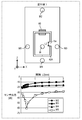
- FIG. 7 is a graph showing a BH curve of ferrite, which is an example of the material of the core 40 according to the embodiment.
- the core of the comparative example has the same configuration as the core 40 according to the present embodiment except that there is no gap S.
- the magnetic flux density of the core of the comparative example has a value L21 in the range of 455 to 465 mT. In this range, the BH curve changes in a curve, and the slope of the tangent line L22 of the BH curve is small. Therefore, in the core of the comparative example, there is a possibility of magnetic saturation when the magnetic flux density is about 0.5T.
- the magnetic flux density of the core 40 having the gap S according to the present embodiment has a value L23 in the range of 180 to 190 mT. Therefore, in the core 40, the magnetic flux density changes in the region R1 where the BH curve is straight and has a large slope. As a result, the core 40 can suppress the occurrence of magnetic saturation.
- FIG. 8 is an explanatory diagram comparing the output V40 of the core 40 according to the embodiment with the output V1 of the core of the comparative example.
- the waveforms of the outputs V40 and V1 are waveforms when a sinusoidal current (amplitude 15A, frequency 5 kHz) is passed through the electric conductor W.
- a sinusoidal current amplitude 15A, frequency 5 kHz
- the peak of the waveform is greatly distorted. This is because magnetic saturation has occurred.
- no distortion occurs in the peak of the waveform. That is, it can be seen that the core 40 according to the embodiment suppresses magnetic saturation as compared with the core of the comparative example.
- the pair of joint surfaces 411, 412, 421, and 431 of the plurality of divided cores 41, 42, and 43 forming the core 40 form the gap S of the core 40. It is parallel to the facing direction DX of the end faces 422 and 432. Thereby, by sliding the pair of joint surfaces 411, 412, 421, and 431 of the plurality of divided cores 41, 42, and 43 with each other, the distance LX of the gap S in the opposite direction DX can be adjusted.
- FIG. 9 is a graph showing the relationship between the gap S of the core 40 of the current sensor 10 and the output V40 according to the embodiment.
- the interval LX of the gap S increases, the sensitivity tends to decrease, but when the interval exceeds a certain size, the decrease in sensitivity saturates. That is, by simply adjusting the interval LX of the gap S, a desired sensitivity characteristic can be realized without being affected by a minute gap at the boundary portion of the plurality of divided cores 41, 42, 43.
- the current sensor 10 can realize a desired sensitivity characteristic even if the core 40 has a boundary portion.
- FIG. 10A and 10B are explanatory views showing a state in which at least one of the divided core 42 and the divided core 43 of the core 40 according to the embodiment is arranged with a step difference with respect to the divided core 41.
- both the split core 42 and the split core 43 are displaced in the width direction X with respect to the split core 41.
- FIG. 10B both the split core 42 and the split core 43 are displaced in the thickness direction Y with respect to the split core 41.
- FIG. 11 shows a current-output line for each of the deviation amounts in the core 40 according to the present embodiment.
- the output V41 when there is no deviation in the core 40 and the output V42 when both the divided core 42 and the divided core 43 are displaced by 0.5 mm in the width direction X with respect to the divided core 41 are displaced by 1.0 mm.
- FIG. 11 shows an output V44 when both the divided core 42 and the divided core 43 are displaced by 0.5 mm in the thickness direction Y with respect to the divided core 41, and an output V45 when both are displaced by 1.0 mm in the thickness direction Y. And are further shown.
- the current-output lines are substantially the same. That is, by adjusting the gap S, even if at least one of the split core 42 and the split core 43 is displaced with a step from the split core 41, the sensitivity characteristic of the current sensor 10 is affected. Absent.
- the gap LX of the gap S can also be determined based on various parameters of the core 40.
- the reference parameters for determining the interval LX of the gap S include, for example, the number of turns of the electric conductor W, the cross-sectional area of the electric conductor W, the shape of the core 40, the distance from the electric conductor W to the core 40, the material of the core 40, and the like. Can be mentioned.
- Examples of the material of the core 40 other than ferrite include Ni—Zn type, Mn—Zn type, iron type and the like.
- the number of the plurality of divided cores 41, 42, 43 is 3 or more, and the pair of joining surfaces 411, 412, 421, and 431 in each pair of divided cores are parallel to the facing direction DX.
- the inside of the C-shaped core 40 can be greatly opened at the time of assembly. Therefore, the electric conductor W can be easily arranged in the C-shaped core 40.
- the pair of joint surfaces 411, 421, 421, and 431 in each pair of split cores are parallel to the facing direction DX, any Even in the pair of split cores, the distance LX of the gap S can be adjusted by sliding the pair of joint surfaces 411, 412, 421, and 431 with each other.
- the current sensor 10 has a non-magnetic bobbin 50 around which the coil 60 is wound.
- the bobbin 50 is provided so as to lock the pair of end faces (the other end faces 422 and 432) of the core 40 and to surround the gap S.
- the adjusted gap S can be stably held. That is, a dedicated member for maintaining the gap LX of the gap S becomes unnecessary, and an increase in the number of parts can be suppressed. Further, since the bobbin 50 is a non-magnetic material, it does not affect the current detection.
- the coil 60 when the coil 60 is directly wound around the core 40 so as to surround the gap S, the winding work becomes difficult because of the gap S.
- the workability can be improved by winding the coil 60 around the non-magnetic bobbin 50 and surrounding the gap S with the bobbin 50.
- the current sensor 10 includes a housing 21 accommodating one divided core 41 among the plurality of divided cores 41, 42, 43, and one or more of the other divided cores 41, 42, 43.
- a housing 22 for accommodating the divided cores 42 and 43 is provided. By integrating the housing 21 and the housing 22, one split core 41 is fixed to the other split cores 42 and 43.
- the plurality of divided cores 41, 42, and 43 in the housing 21 and the housing 22 are less likely to be displaced from each other after assembly. Therefore, since the interval LX of the gap S of the core 40 is stabilized for a long period of time, the sensitivity characteristic of the current sensor 10 can be maintained for a long period of time.
- the core 40 is formed by joining a plurality of divided cores 41, 42, 43.
- a plurality of divided cores 41, 42, and 43 are assembled so as to surround the electric conductor W to form the core 40 so that the electric conductor W penetrates into the C-shaped core 40. Can be easily placed in.
- the core configuration is not limited to the configuration described in the above embodiment. Therefore, a modified example of the core will be described below, focusing on the difference from the above embodiment.
- the same parts as those in the above embodiment may be designated by the same reference numerals and the description thereof may be omitted.
- the current sensor 10 includes a core 40 including three divided cores 41, 42, and 43.
- the current sensor of the first modification includes a core 40A composed of two divided cores 44 and 45.
- FIG. 12 is a plan view of the core 40A according to the first modification.
- FIG. 12 corresponds to FIG.
- the core 40A is composed of two divided cores 44 and 45.
- the split core 44 is provided with a gap Sa in the lower portion of the rectangular frame shape in the positive direction of the X-axis.
- one tip surface 441 faces the positive side of the X-axis, and the other tip face 442 faces downward, that is, the negative side of the Z-axis.
- One tip surface 441 is a plane parallel to the YZ plane.
- the other tip surface 442 is a plane parallel to the XY plane.
- One tip surface 441 is a joint surface to be joined to the other split core 45.
- the split core 45 has a substantially L-shape.
- One end surface 451 of the split core 45 is a joint surface joined to the tip surface 441 of the split core 44.
- One end surface 451 of the split core 45 is a plane parallel to the YZ surface.
- the other end surface 452 of the split core 45 is joined to the tip surface 441 of the split core 44 in a posture of facing upward.
- the other end surface 452 of the split core 45 is a plane parallel to the XY plane.
- a gap Sa is formed between the tip surface 442 of the split core 44 and the other end surface 452 of the split core 45.
- the pair of end faces (tip surface 442, other end surface 452) forming the gap Sa face each other in the opposite direction DZ of the Z axis via the gap Sa.
- the coil 60 is wound around the upper part of the split core 45.
- the coil 60 may be directly wound around the upper part of the split core 45, or may be indirectly wound around the upper part of the split core 45 via a bobbin.
- the current sensor 10 includes a core 40 in which the gap S is provided in the center of the frame-shaped upper frame portion.
- the current sensor in the second modification includes a core 40B in which the gap Sb is provided in the center of the frame-shaped lower frame portion.
- FIG. 13 is a plan view of the core 40B according to the second modification. FIG. 13 corresponds to FIG.
- the core 40B has a C-shape having a gap Sb located at the center of the lower frame portion of the rectangular frame shape in a plan view. Specifically, the core 40B has a structure in which the core 40 is inverted upside down, and is a structure equivalent to the core 40. Further, in the core 40B according to the second modification, the coil 60 is wound around the upper portion of the divided core 41. The coil 60 may be directly wound around the upper part of the split core 41, or may be indirectly wound around the upper part of the split core 41 via a bobbin.
- FIG. 14A is an explanatory diagram showing the influence of other electric conductors W2, W3, W4, and W5 on the core 40A of the modified example 1.
- FIG. 14B is an explanatory diagram showing the influence of other electric conductors W2, W3, W4, and W5 on the core 40B of the modified example 2.
- FIG. 14C is an explanatory diagram showing the influence of other electric conductors W2, W3, W4, and W5 on the core 40 according to the embodiment.
- the other electric conductors W2 are arranged above the cores 40, 40A, 40B.
- the other electric conductors W3 are arranged in the positive direction of the X-axis of the cores 40, 40A, and 40B.
- the other electric conductor W4 is arranged below the cores 40, 40A, and 40B.
- the other electric conductor W5 is arranged in the direction of the minus side of the X-axis of the cores 40, 40A, and 40B.
- the electric conductors W2 to W4 other than the other electric conductors W5 are larger than -20 dB, and it can be seen that the detection of the current of the electric conductor W is affected.
- the electric conductors W2 and W4 other than the other electric conductors W3 are larger than ⁇ 20 dB, and it can be seen that the detection of the current of the electric conductor W is affected. It is presumed that these effects are caused by the intrusion of magnetic flux from the external electric conductors W2 to W5 into the gaps Sa and Sb.
- the output is -20 dB or less and the fluctuation is small in all of the other electric conductors W2 to W4.
- the coil 60 is wound around the gap S of the core 40, so that the coil 60 blocks the magnetic flux from the external electric conductors W2 to W5 toward the gap S, and suppresses the influence of the magnetic flux. be able to. That is, the core 40 according to the embodiment is preferable in suppressing the influence from other electric conductors W2 to W5.
- 15 to 17 are explanatory views showing the status of the cores 40, 40A, and 40B of each verification case and the output of the sensor of each verification case.
- the output of the sensor in each verification case shows the influence of the other electric conductors W2 to W4 on the detection of the current flowing through the electric conductor W.
- the coil 60 is wound around the upper part of the core 40B according to the second modification.
- the coil 60 is wound around the upper part of the core 40 according to the embodiment.
- the coil 60 is wound around the upper part of the core 40A according to the first modification. That is, in the cases A and C, the gaps Sa and Sb are totally exposed from the coil 60, but in the case B, the gap S is totally covered by the coil 60.
- the coil 60 is wound around the lower part of the core 40B according to the second modification.
- the coil 60 is wound around the lower part of the core 40 according to the embodiment.
- the coil 60 is wound around the lower part of the core 40A according to the first modification. That is, in the cases E and F, the gaps S and Sb are totally exposed from the coil 60, but in the case D, the gap Sa is totally covered by the coil 60.
- the coil 60 is wound around the central portion of the core 40B according to the second modification on the positive side of the X axis.
- the coil 60 is wound around the central portion of the core 40 according to the embodiment on the positive side of the X-axis.
- the coil 60 is wound around the center portion on the positive side of the X-axis of the core 40A according to the first modification. That is, in the cases G and H, the gaps S and Sa are totally exposed from the coil 60, but in the case I, the gap Sb is totally covered by the coil 60.
- the current sensor 10 includes a core 40 (40B, 40B) through which the electric conductor W is penetrated, and a coil 60 arranged so as to be wound around the core 40 (40A, 40B).
- the core 40 (40A, 40B) has a C-shape having a gap S, Sa, Sb in a part.
- the coil 60 is wound at a position surrounding the gap S (Sa, Sb).
- the coil 60 Since the coil 60 is wound around the gap S (Sa, Sb) of the core 40 (40A, 40B), the coil 60 transmits the magnetic flux from the external electric conductors W2 to W5 toward the gap S (Sa, Sb). By blocking, the influence of the magnetic flux, that is, the influence of external noise can be suppressed.
- a pair of end faces (the other end surface 422, 432, the tip end surface 442, the other end surface 452) of the core 40 (40A, 40B) forming the gap S (Sa, Sb) are arranged in the coil 60.
- both ends of the gap S (Sa, Sb) are covered with the coil 60.
- the coil 60 more reliably blocks the magnetic flux from the external electric conductors W2 to W5 toward the gap S (Sa, Sb). Therefore, the influence of the magnetic flux from the external electric conductors W2 to W5 can be suppressed more reliably.
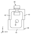
- FIG. 18 is a perspective view of another current sensor 510 according to the embodiment.
- FIG. 19 is a cross-sectional view taken along the line XIX-XIX of the current sensor 510 shown in FIG.
- FIG. 20 is a cross-sectional view taken along the line XX-XX of the current sensor 510 shown in FIG.
- the current sensor 510 includes a housing 520 and a sensor unit 530 housed in the housing 520.
- FIG. 21 is a perspective view of the housing 520.
- the housing 520 has a housing 21 and 22 divided in two in the Z-axis direction, and a hinge 551 connecting the housing 21 to the housing 22.
- the hinge 551 connects one of the pair of lower wall portions 214 of the main body portion 211 of the housing 21 to one of the pair of upper wall portions 224 of the main body portion 221 of the housing 22.
- the housing 21 includes a box-shaped main body portion 211 having a space 21s in which the positive direction of the Z axis is open, and a locking portion 212 that is locked to the housing 22.
- the locking portion 212 is located on the opposite side of the hinge 551. Specifically, the locking portion 212 is provided on the other side of the pair of lower wall portions 214 of the main body portion 211 of the housing 21.
- a split core 41 which is a part of the sensor unit 530, is fitted and fixed between the inner wall portions 215.
- the housing 22 has a box shape having a space 22s in which the negative direction of the Z axis is open.
- the housing 22 has a pair of upper wall portions 223 facing each other in the Y-axis direction, a pair of upper wall portions 224 facing each other in the X-axis direction, and a floor plate portion 229.
- the upper wall portions 223 and 224 are connected to each other and extend from the bottom plate portion 229 to the minus side of the Z axis.
- the upper wall portion 223 and 224 and the bottom plate portion 229 surround the space 22s.
- Engagement protrusions 228a are provided on the other outer surface of the pair of upper wall portions 224 of the housing 22.
- the locking portion 212 of the housing 21 extends from the outer surface of the lower wall portion 214 in the positive direction of the Z axis.
- the locking portion 212 has a substantially U-shape.
- the split cores 42 and 43 are firmly fixed to the bobbin 50 by being press-fitted into the space 50s of the bobbin body 51 so as to come into contact with the inner bottom portion 53 of the bobbin 50.
- the split cores 42 and 43 are housed in the space 50s with a gap of 50t from the bobbin main body portion 51.
- the split cores 42 and 43 are not fixed to the bobbin 50 before being housed in the housing 22, but the split core 42, the split core 43, and the bobbin 50 are used to maintain the shape of the sensor unit 530, respectively. Is positioned on the housing 22 and firmly fixed.
- the current sensor 510 is provided with an inner lid 531 that covers the bobbin 50 at the opening of the housing 22.
- the inner lid 531 can prevent foreign substances having conductivity or magnetism from entering the housing 22, protect the coil 60, and prevent the detection accuracy of the current sensor 530 from being affected.
- the housing 22 has a rib 610 that projects from the main body 221 toward the space 22s and positions the split core 41 (42).
- the ribs 610 position the split cores 41 and 42 with respect to the housing 22 and the bobbin 50.
- the bobbin 50 and the split cores 41 and 42 inserted in the space 50s of the bobbin 50 are inserted so as to press-fit the housing 22, so that the split core 42, the split core 43, and the bobbin 50 are assembled. Each is positioned on the housing 22 and firmly fixed.
- the split cores 41 and 42 scrape the housing 22 to generate shavings, which may be sandwiched between the facing surface 612a of the rib 610 and the split core 41 (42). If shavings are generated between the facing surface 612a of the rib 610 and the split core 41 (42), the positions of the split cores 41 and (42) with respect to the rib 610 shift and the shape of the core 40 cannot be maintained, or the housing There is a concern that the locking portion 212 of the body 21 may not reach the engaging projection 228a of the housing 22 and may become engaged.
- the rib 610 has a base portion 611 protruding from the main body portion 221 toward the space 22s and a positioning portion 612 extending from the base portion 611 toward the split core 41 (42).
- the positioning portion 612 has a facing surface 612a that faces and abuts the split core 41 (42).
- the positioning portion 612 is separated from the main body portion 221 via a slit 613 extending from the facing surface 612a.
- the housing 21 is a protrusion configured so that the housing 21 is integrated with the housing 22 and is fitted in the space 22s so as to abut the main body 221 of the housing 22. It has 230a and 230b.
- the protrusion 230a is not provided with the hinge portion 551 of the housing 21, and protrudes from the lower wall portion 214 on the opposite side of the hinge portion 551.
- the protrusion 230b extends from the bottom plate 219 of the housing 21.
- the protrusions 230a and 230b come into contact with the main body 221 of the housing 22 and particularly the upper wall 223 when the housing 21 is integrated with the housing 22.
- the housings 21 and 22 are integrated and fixed to each other even when a mechanical impact such as dropping or transportation is applied, and as a result, the relative displacements of the divided cores 41, 42, 43 are displaced. To prevent the split cores 41, 42, and 43 from being chipped.
- FIG. 23 is an enlarged cross-sectional view of the current sensor 510 shown in FIG. It is preferable that the current sensor 510 further includes a cushion 541 provided between the main body 211 of the housing 21 and the split core 41.
- the cushion 541 comes into contact with the lower wall portion 214 and the split core 41, particularly between the lower wall portion 214 and the split core 41 of the main body portion 211.
- the split core 41 can be reliably positioned with respect to the housing 21 and fixed to the housing 21, and the split cores 41, 42, and 43 are prevented from cracking.
- FIG. 23 is a perspective view of another sensor unit 530 of the current sensor 510.
- substantially the same parts as the sensor unit 30 shown in FIG. 4 are designated by the same reference numbers.
- the joint surface 411 of the split core 41 is joined to the joint surface 421 of the split core 42, and the joint surface 412 of the split core 41 is joined to the joint surface 431 of the split core 43.
- Both ends 411a of the joint surface 411 of the split core 41 in the Y-axis direction are chamfered.
- One of the 411a at both ends may not be chamfered.
- Both ends 412a of the joint surface 412 of the split core 41 in the Y-axis direction are chamfered.
- One of the 412a at both ends may not be chamfered. As a result, even if a mechanical impact such as dropping or transportation is applied, it is possible to prevent the corners of the divided cores 41, 42, 43 from coming into direct contact with each other, and to prevent the divided cores 41, 42, 43 from being chipped.
- FIG. 24 is a perspective view of still another sensor unit 630 of the current sensor 510.
- substantially the same parts as the sensor unit 530 shown in FIG. 23 are designated by the same reference numbers.
- Both ends 421a of the joint surface 421 of the split core 42 in the Y-axis direction are chamfered. One of both ends 421a may not be chamfered.
- Both ends 431a of the joint surface 431 of the split core 43 in the Y-axis direction are chamfered. One of both ends 431a may not be chamfered.
Abstract
電流センサは、電気導体に流れる電流を検出する。この電流センサは、電気導体が貫通されるように構成された中空部を有するコアと、コアに巻き付けられたコイルとを備える。コアは、中空部に繋がる隙間を有するC字形状を実質的に有する。コアは隙間を介して対向方向で互いに対向する一対の端面を有する。コアは互いに接合された複数の分割コアを有する。複数の分割コアのうちの互いに隣接するそれぞれの対の分割コアは対向方向に平行な接合面をそれぞれ有する。この電流センサは、所望の感度特性を実現することが可能である。
Description
本開示は、電流センサに関する。
特許文献1は、一部にコイルが巻かれた環状のコアを貫通するように電気導体を配置した従来の電流センサを開示している。この電流センサにおいては、環状のコア内に電気導体を配置しやすくするために、環状のコアが分割されている。組立時においては、分割されたコアにまず電気導体が配置され、その後、コアが組み立てられることで、環状のコア内に電気導体が貫通するように配置される。
電流センサは、電気導体に流れる電流を検出する。この電流センサは、電気導体が貫通されるように構成された中空部を有するコアと、コアに巻き付けられたコイルとを備える。コアは、中空部に繋がる隙間を有するC字形状を実質的に有する。コアは隙間を介して対向方向で互いに対向する一対の端面を有する。コアは互いに接合された複数の分割コアを有する。複数の分割コアのうちの互いに隣接するそれぞれの対の分割コアは対向方向に平行な接合面をそれぞれ有する。
この電流センサは、所望の感度特性を実現することが可能である。
以下で説明する実施の形態は、いずれも本開示の一具体例を示すものである。以下の実施の形態で示される数値、形状、材料、構成要素、構成要素の配置位置及び接続形態、工程、工程の順序などは、一例であり、本開示を限定する主旨ではない。また、以下の実施の形態における構成要素のうち、本開示の一形態に係る実現形態を示す独立請求項に記載されていない構成要素については、任意の構成要素として説明される。本開示の実現形態は、現行の独立請求項に限定されるものではなく、他の独立請求項によっても表現され得る。
[実施の形態]
[電流センサの構造]
図1は、実施の形態に係る電流センサ10の概略構成を示す斜視図である。図2は電流センサ10の分解斜視図である。図3は、図1に示す電流センサ10の線III-IIIにおける断面図である。図1では、検出対象であるワイヤ状の電気導体Wを破線で示している。なお、以降の説明においては、X軸方向を幅方向Xと称し、Y軸方向を厚み方向Yと称し、Z軸方向を上下方向Zと称する場合がある。
[電流センサの構造]
図1は、実施の形態に係る電流センサ10の概略構成を示す斜視図である。図2は電流センサ10の分解斜視図である。図3は、図1に示す電流センサ10の線III-IIIにおける断面図である。図1では、検出対象であるワイヤ状の電気導体Wを破線で示している。なお、以降の説明においては、X軸方向を幅方向Xと称し、Y軸方向を厚み方向Yと称し、Z軸方向を上下方向Zと称する場合がある。
電流センサ10は、電気導体Wを流れる交流電流を検出するCurrent Transformer(CT)方式の電流センサである。電流センサ10は、筐体20と、筐体20に収容されたセンサユニット30とを備えている。
筐体20は、例えば非磁性体の樹脂により、全体として略直方体状に形成されている。筐体20は、厚み(Y軸方向での長さ)が全体として一定である。筐体20は、筐体21、22にZ軸方向で二分割されており、Z軸のマイナス側の方向の部位が筐体21であり、Z軸のプラス側の方向部位が筐体22である。
筐体21は、Z軸のプラス側の方向が開放された空間21sを有する箱形状を有する本体部211と、筐体22に係止される一対の係止部212とを備えている。本体部211は、Y軸方向で互いに対向する一対の下壁部213と、X軸方向で互いに対向する一対の下壁部214と、底板部219とを有する。下壁部213、214は互いに繋がっており底板部219からZ軸のプラス側に延びる。下壁部213、214と底板部219とは空間21sを囲む。また、筐体21の内部には、下壁部213と平行な一対の内壁部215が設けられている。一対の内壁部215は、Y軸方向で所定の間隔をあけて配置されている。一対の内壁部215の間には、センサユニット30の一部が嵌め込まれ、固定される。また、一対の下壁部213には、半円弧形状を有する切欠き部213aが形成されている、一対の内壁部215には、半円弧状の切欠き部215aが形成されている。
一対の係止部212は、一対の下壁部214の外側面からZ軸のプラス側の方向に延在する。一対の係止部212は、略U字形状を有する。一対の係止部212のそれぞれは、筐体22の複数の係合突起228a、228bに係合することで、筐体21と筐体22とを一体化して互いに固定する。
筐体22は、Z軸のマイナス側の方向が開放された空間22sを有する箱形状を有する。筐体22は、Y軸方向で互いに対向する一対の上壁部223と、X軸方向で互いに対向する一対の上壁部224と、床板部229とを有する。上壁部223、224は互いに繋がっており底板部229からZ軸のマイナス側に延びる。上壁部223、224と底板部229とは空間22sを囲む。
一対の上壁部223のそれぞれには半円弧状の切欠き部223aが形成されている。切欠き部223aは、筐体21と筐体22とが組み立てられた状態では、筐体21の切欠き部213aとともに図1に示す貫通孔20hを形成する。貫通孔20h内に電気導体Wが挿通される。この状態では、筐体21の一対の内壁部215の切欠き部215a内にも電気導体Wが収容される。切欠き部213a、215a、223aは、電気導体Wを支持する支持部としても機能する。
一対の上壁部224の内面には、センサユニット30をY軸方向で挟む一対の突起224aがそれぞれ形成されている。図3では、一対の突起224aのうち、Y軸のプラス側の方向の突起224aのみを図示している。一対の突起224aはZ軸方向に延在している。一対の突起224aは、Y軸方向に互いに所定の間隔をあけて配置されている。一対の突起224aの間にはセンサユニット30の一部が嵌め込まれ、固定されている。
また、一対の上壁部224の内面には、センサユニット30の上下方向の位置ずれを規制する規制凸部224bがそれぞれ設けられている。規制凸部224bは、一対の突起224aの間に配置されており、Z軸方向に延在している。規制凸部224bの下端面が、センサユニット30の上端面に当接することで、センサユニット30の上下方向Zの筐体20に対する位置ずれを規制する。
一対の上壁部224のそれぞれの外側面には、三つの係合突起228a、228bが設けられている。三つの係合突起228a、228のうち、二つの係合突起228bは上壁部224の下端に設けられ、Y軸方向に互いに所定の間隔をあけて配置されている。二つの係合突起228bは、筐体21の係止部212をY軸方向で挟持する。一方、残りの一つの係合突起228aは、二つの係合突起228bのY軸方向の中央付近の上方に配置されている。係合突起228bは、筐体21の係止部212の上部を下方から支持する。三つの係合突起228a、228bがこのような状態で係止部212に係合することで、筐体21と筐体22との相対的な位置ずれを規制し、両者を一体化して互いに固定している。
次に、センサユニット30について説明する。図4は、実施の形態に係るセンサユニット30の概略構成を示す斜視図である。図5は、実施の形態に係るセンサユニット30の分解斜視図である。図6は、実施の形態に係るセンサユニット30の平面図である。
図4から図6に示すように、センサユニット30は、コア40と、ボビン50と、コイル60とを備えている。
コア40は、例えばフェライトなどの磁性体によりなり、中空部40hと、中空部40hに繋がる隙間Sとを有するC字形状を実質的に有する。具体的には、コア40は、平面視で矩形枠形状を有する。隙間Sは、矩形枠形状の上枠部の中央に設けられている。コア40の外側の四隅の断面は、先端が尖った角部であり、内側の四隅の断面は円弧形状の角部である。なお、外側の四隅の断面は円弧形状を有していてもよいし、内側の四隅の断面が先端の尖った角部であってもよい。また、コア40の外形は、矩形枠形状でなくとも、その他の多角枠形状、円形枠形状、長円枠形状、楕円枠形状等の他の枠形状を有していてもよい。
コア40は、互いに接合された複数の分割コア41、42、43よりなる。具体的には、分割コア41は、コア40の下部をなし、分割コア42、43はコア40の上部をなす。
分割コア41は、上方が開放された略U字形状を有する。分割コア41の一対の先端面は、上方を向いた姿勢に形成されており、他の分割コア42、43と接合される接合面411、412である。一対の接合面411、412は、X軸とY軸とを含むXY平面に平行な平面である。接合面411は、X軸のマイナス側の方向に配置されており、接合面412は、X軸のプラス側の方向に配置されている。
分割コア42は、略L字形状を有する。分割コア42の一端面は、分割コア41の接合面411に接合される接合面421である。分割コア42の接合面421は、XY面に平行な平面である。分割コア42の他端面422が、X軸のプラス側の方向を向く姿勢で、分割コア41の接合面411に接合されている。分割コア42の他端面422は、Y軸とZ軸とを含むYZ平面に平行な平面である。
分割コア43は、略L字形状を有する。分割コア43は、分割コア42と同じ部材である。分割コア43の一端面は、分割コア41の接合面412に接合される接合面431である。分割コア43の接合面431は、XY面に平行な平面である。分割コア43の他端面432が、X軸のマイナス側の方向を向く姿勢で、分割コア41の接合面412に接合されている。分割コア43の他端面432は、YZ平面に平行な平面である。
複数の分割コア41、42、43のうちの互いに隣接するそれぞれの対の分割コアは対向方向DXに平行な接合面をそれぞれ有する。詳細には、分割コア42の他端面422は、分割コア43の他端面432とX軸と平行な対向方向DXで対向している。コア40において分割コア42の他端面422と分割コア43の他端面432との間には隙間Sが形成されている。すなわち、コア42の他端面422は隙間Sを介して分割コア43の他端面432と対向方向DXで対向する。隙間Sの対向方向DXの間隔LX(X軸方向の長さ)は、電流センサ10の組立前に調整しておくことで、所望の感度特性を実現することが可能である。上述したように、分割コア41の接合面411と、分割コア42の接合面412の双方は、XY平面に平行な平面である。このため、分割コア41、42の接合面411、421同士をスライドさせて、分割コア42を移動することで分割コア42の他端面422の位置をX軸の方向に沿って調整する、つまり、隙間Sの間隔LXを調整することができる。これは、分割コア41の接合面412と、分割コア43の接合面431との関係においても同様である。本実施の形態では、一対の分割コア42、43の外側面が、分割コア41の外側面と面一となった状態で隙間Sの間隔LXが、所望の感度特性を実現する。なお、所望の感度特性を実現するためには、隙間S内に導電性の部材を配置しないことが望ましい。
分割されたコアよりなる環状のコアには、組立により境界部分が生じている。この境界部分には、僅かなギャップがあるために、当該境界部分が電流検出に影響を与え、感度が低下することがある。
実施の形態における電流センサ10では、前述のように、所望の感度特性を実現することが可能である。
実施の形態では、分割コア41の接合面411と、分割コア42の接合面421の双方がXY平面に平行な平面である。しかしながら、分割コア41の接合面411と、分割コア42の接合面421の双方は、X軸の方向に平行に延設されつつ、Y軸の方向に対して傾斜していてもよい。この場合においても、分割コア41、42の接合面411、421同士をスライドさせて、分割コア42を移動させれば当該分割コア42の他端面422の位置をX軸方向に沿って調整することができる。分割コア41の接合面411と、分割コア42の接合面421の双方は、相互に面接触する限り湾曲面であってもよい。
ボビン50は、樹脂等の非磁性体からなる。具体的には、ボビン50は、角筒状のボビン本体51と、ボビン本体51のX軸の方向の両端部から張り出した一対の鍔部52とを備えている。一対の鍔部52は、ボビン本体51の上記両端部からX軸に直角の方向の全周にわたって張り出している。ボビン本体51は、X軸の方向に延びる。ボビン本体51の外周には、X軸の方向に延びる巻回軸60cを中心にコイル60がボビン本体51に巻きつけられている。巻きつけられたコイル60は、一対の鍔部52の間に収容されている。ボビン50すなわちボビン本体51には、巻線軸60cに沿って一対の内部空間50sが設けられている。
図3に示すように、ボビン本体51の内部の中央には、ボビン本体51の一対の内部空間50sを互いに遮断する内底部53が設けられている。ボビン本体51の一対の内部空間50sが開口する一対の開口50pには、分割コア42の端面422を含む端部と分割コア43の端面432を含む端部とが内底部53に付き当てられた状態でボビン本体部51に当接するようにそれぞれ嵌め込まれる。つまり、ボビン50は、コア40の一対の他端面422、432を係止し、かつ隙間Sを囲むように設けられている。これにより、分割コア42の他端面422と分割コア43の他端面432との間の隙間Sが内底部53によって規定される。内底部53における厚み(X軸方向の長さ)は、隙間Sの間隔LXに対応した値となっている。つまり、所望の感度特性を実現できる間隔LXとなるように、内底部53の厚みを予め調整する。
コイル60は、導電性の配線であり、ボビン本体51に対して、多重に巻きつけられている。前述したように、ボビン本体51の一対の内部空間50s内には分割コア42の端部と分割コア43の端部とがそれぞれ圧入されて嵌め込まれているので、コア40の一対の他端面422、432は、コイル60の内方に配置されている。
電流センサ10の動作を以下に説明する。電気導体Wに流れる交流電流によってコア40内に磁束が発生すると、コイル60には、当該磁束を打ち消すように交流電流が流れる。コイル60の両端部には、計測装置が接続されており、計測装置が、コイル60を流れる交流電流に基づいて、電気導体Wを流れる交流電流を検出し計測することができる。
[電流センサの組立方法]
次に、電流センサ10の組立方法について説明する。電流センサ10の組立は、作業者または組立装置で行うことができるが、ここでは作業者が組み立てる場合について説明する。
次に、電流センサ10の組立方法について説明する。電流センサ10の組立は、作業者または組立装置で行うことができるが、ここでは作業者が組み立てる場合について説明する。
まず作業者は、ボビン本体51に所定の巻き数だけコイル60が巻き付けられたボビン50を準備する。作業者は、ボビン本体51の一対の開口50pに分割コア42の端部と分割コア43の端部とをそれぞれ嵌め込む。この際、作業者は、分割コア42の端面422及び分割コア43の端面432を内底部53に突き当てる。これにより、他端面422、432が間隔LXの隙間Sをあけて互いに対向する。
その後、作業者は、筐体22に、一対の分割コア42、43及びボビン50を組み付ける。具体的には、作業者は、一体化された一対の分割コア42、43及びボビン50を、筐体22の下方から一対の突起224aの間に嵌め込む。このとき、作業者は、一対の分割コア42、43の上端面が、筐体22の規制凸部224bに当接するまで、一対の分割コア42、43及びボビン50を、筐体22に対してスライドさせる。これにより、一対の分割コア42、43及びボビン50が筐体22内で固定される。分割コア42、43はボビン50の内底部53に付き当たるように、かつボビン本体51に当接するように空間50sに圧入されて嵌め込まれてボビン50に強固に固定されている。したがって、筐体22に対してボビン50と分割コア42、43を容易に固定することができる。
一方、作業者は、筐体21に分割コア41を組み付ける。具体的には、作業者は、分割コア41を、筐体21の上方から一対の内壁部215の間に嵌め込む。このとき、作業者は、分割コア41の下端面が、筐体21の内底面に当接するまで、分割コア41を、筐体21に対してスライドさせる。これにより、分割コア41が筐体21内で固定される。
次いで、作業者は、筐体21と分割コア41に電気導体Wを組み付ける。具体的には、作業者は、電気導体Wを筐体21の切欠き部213a、215a、223a内に収容する。これにより、電気導体Wは、切欠き部213a、215a、223aによって支持されて、分割コア41の開放端部側に配置された状態となる。
次いで、作業者は、電気導体Wを支持した状態の筐体21に筐体22を組み付ける。組み付け時においては、作業者は、筐体22の各上壁部224に備わる複数の係合突起228a、228bに、筐体21の係止部212を係合させる。これにより、筐体21と筐体22とが一体化される。筐体21と筐体22との内部では、分割コア41の接合面411に分割コア42の接合面421が接合され、分割コア41の接合面412に分割コア43の接合面431が接合されている。これにより、電流センサ10の組立が完了する。
電流センサ10では、落下や運搬等の機械的な衝撃が加わって筐体21、22が互いに相対的に位置ずれすると、接着されておらずに互いに当接している分割コア41の接合面411、412と分割コア42、43の接合面421、431で分割コア41、42、43が割れて欠ける場合がある。電流センサ10では、前述のように三つの係合突起228a、228bが係止部212に係合することで、筐体21と筐体22との相対的な位置ずれを規制し、両者を一体化して互いに固定し、結果として分割コア41、42、43の相対的な変位を防止して分割コア41、42、43が欠けることを防止する。
なお、本実施の形態では、接合面を接着せずに単に当接させていることで接合面が接合されているが、磁性を有する接着剤で接合面同士を接着してもよいし、接合面同士を溶着してもよい。接着後あるいは溶着後であっても、接着痕あるいは溶着痕を解析することで、接着前あるいは溶着前の接合面同士を特定することが可能である。なお、接合面同士を単に当接させている場合であれば、分割コアの分離によりコアを容易に分解でき、例えばメンテナンス時の作業性を高めることができる。
[効果など]
以上のように、本実施の形態に係る電流センサ10は、電気導体Wが貫通されるコア40と、コア40の周囲に巻きつけられるように配置されたコイル60とを備える。コア40は、複数の分割コア41、42、43が接合されることで、一部に隙間Sを有するC字形状を有する。複数の分割コア41、42、43の一対の接合面411、412、421、431(具体的には、接合面411及び接合面421の対、接合面412及び接合面431の対)は、隙間Sをなすコア40の一対の端面である他端面422、432が対向する対向方向DXに平行である。
以上のように、本実施の形態に係る電流センサ10は、電気導体Wが貫通されるコア40と、コア40の周囲に巻きつけられるように配置されたコイル60とを備える。コア40は、複数の分割コア41、42、43が接合されることで、一部に隙間Sを有するC字形状を有する。複数の分割コア41、42、43の一対の接合面411、412、421、431(具体的には、接合面411及び接合面421の対、接合面412及び接合面431の対)は、隙間Sをなすコア40の一対の端面である他端面422、432が対向する対向方向DXに平行である。
本発明者は、鋭意検討を重ねて、複数の分割コア41、42、43の境界部分よりも極度に大きな隙間Sをコア40の一部に設けることで、境界部分を無視できることを見出した。図7は、実施の形態に係るコア40の材料の一例であるフェライトのBH曲線を示すグラフである。
ここで、隙間Sのない比較例のコアを準備する。比較例のコアは、隙間Sがない以外は、本実施の形態に係るコア40と同等の構成である。比較例のコアの磁束密度は455~465mTの範囲の値L21を有する。この範囲では、BHカーブが曲線的に変化しており、BH曲線の接線L22の傾きは小さい。このため、比較例のコアでは、磁束密度が0.5T程度で磁気飽和するおそれがある。
一方、本実施の形態に係る隙間Sを有するコア40の磁束密度は、180~190mTの範囲の値L23となる。このため、コア40では、BH曲線が直線的であり大きな傾きを有する領域R1で磁束密度が変化する。これにより、コア40では磁気飽和の発生を抑制することができる。
図8は、実施の形態に係るコア40の出力V40と、比較例のコアの出力V1とを比較した説明図である。なお、出力V40、V1の波形は、電気導体Wに正弦波の電流(振幅15A、周波数5kHz)を流したときの波形である。図8に示すように、比較例のコアの出力では、波形のピークが大きく歪んでいる。これは磁気飽和が発生しているためである。一方、実施の形態に係るコア40の出力V40では、波形のピークに歪みが発生していない。つまり、実施の形態に係るコア40では、比較例のコアと比べて磁気飽和が抑制されていることが分かる。
また、本実施の形態に係る電流センサ10では、コア40をなす複数の分割コア41、42、43の一対の接合面411、412、421、431が、コア40の隙間Sをなす一対の他端面422、432の対向方向DXに平行である。これにより、複数の分割コア41、42、43の一対の接合面411、412、421、431を互いにスライドさせることで、隙間Sの対向方向DXの間隔LXを調整することができる。
図9は、実施の形態に係る電流センサ10のコア40の隙間Sと出力V40の関係を示すグラフである。図9に示すように、隙間Sの間隔LXが大きくなると、感度は低下していく傾向ではあるが、ある程度の大きさの間隔以上になると感度の低下が飽和している。つまり、隙間Sの間隔LXを調整するだけで、複数の分割コア41、42、43の境界部分の微少な隙間に影響されることなく、所望の感度特性を実現できる。
以上のことから、本実施の形態に係る電流センサ10は、コア40に境界部分があったとしても、所望の感度特性を実現することができる。
また、同一種のコア40であっても、隙間Sの間隔LXを調整すれば多様な感度特性を得ることができるので、他の種類の電流センサでの部品を共通化することも可能である。
隙間Sを調整したことによって、分割コア42及び分割コア43の少なくとも一方が分割コア41に対して段差を持ってずれて配置される場合がある。図10Aと図10Bは、実施の形態に係るコア40の分割コア42及び分割コア43の少なくとも一方が分割コア41に対して段差を持ってずれて配置された状態を示す説明図である。具体的には、図10Aでは、分割コア42及び分割コア43の両者が、分割コア41に対して幅方向Xにずれている。また、図10Bでは、分割コア42及び分割コア43の両者が、分割コア41に対して厚み方向Yにずれている。本発明者は、分割コア42及び分割コア43の両者が、分割コア41に対するずれているずれ量を変更して、それぞれの電流-出力線を求めた。図11は、本実施の形態に係るコア40におけるずれ量のそれぞれでの電流-出力線を表す。ここでは、コア40にずれがない場合の出力V41と、分割コア42及び分割コア43の両者が分割コア41に対して幅方向Xに0.5mmずれた場合の出力V42と、1.0mmずれた場合の出力V43とを示す。図11は、分割コア42及び分割コア43の両者が分割コア41に対して厚さ方向Yに0.5mmずれた場合の出力V44と、厚さ方向Yに1.0mmずれた場合の出力V45とをさらに示す。図11に示すように、いずれの場合においても、電流-出力線は概ね同一となっている。つまり、隙間Sを調整したことによって、分割コア42及び分割コア43の少なくとも一方が、分割コア41に対して段差を持ってずれて配置されたとしても、電流センサ10の感度特性に影響を及ぼさない。
なお、隙間Sの間隔LXは、コア40の各種のパラメータを基準として決定することも可能である。隙間Sの間隔LXを決める基準となるパラメータとしては、例えば、電気導体Wの巻き数、電気導体Wの断面積、コア40の形状、電気導体Wからコア40までの距離、コア40の材質などが挙げられる。フェライト以外のコア40の材質としては、Ni-Zn系、Mn-Zn系、鉄系等が挙げられる。
また、複数の分割コア41、42、43の数は3以上であり、各対の分割コアにおける一対の接合面411、412、421、431は、対向方向DXに平行である。
複数の分割コア41、42、43の数が3以上であるので、組立時に、C字形状のコア40の内部を大きく開放することができる。このため、電気導体Wを、C字状のコア40内に容易に配置することができる。
また、各対の分割コア(分割コア41及び分割コア42の対、分割コア41と分割コア43の対)における一対の接合面411、412、421、431が、対向方向DXに平行なので、いずれの対の分割コアにおいても、その一対の接合面411、412、421、431を互いにスライドさせれば、隙間Sの間隔LXを調整することができる。
また、電流センサ10は、コイル60が巻き付けられる非磁性体のボビン50を有する。ボビン50は、コア40の一対の端面(他端面422、432)を係止し、かつ隙間Sを囲むように設けられている。
これによれば、コイル60が巻きつけられた非磁性体のボビン50によって、コア40の一対の端面が係止されているので、調整後の隙間Sを安定して保持することができる。つまり、隙間Sの間隔LXを保持するための専用の部材が不要となり、部品点数の増加を抑制することができる。さらに、ボビン50は、非磁性体であるため、電流検出に対して影響も与えない。
ここで、隙間Sを囲むように、コア40に対してコイル60を直接巻き付ける場合には、隙間Sがあるがゆえに巻き付け作業が困難となる。しかしながら、非磁性体のボビン50に対してコイル60を巻き付け、ボビン50によって隙間Sを囲むことにより、その作業性を高めることができる。
また、電流センサ10は、複数の分割コア41、42、43のうち、一つの分割コア41を収容する筐体21と、複数の分割コア41、42、43のうち、他の1つ以上の分割コア42、43を収容する筐体22とを備える。筐体21と、筐体22とが一体化されることで、一つの分割コア41が、他の分割コア42、43と固定されている。
これにより、筐体21及び筐体22内で複数の分割コア41、42、43が組立後に互いに位置ずれしにくくなる。したがって、コア40の隙間Sの間隔LXが長期的に安定化されるため、電流センサ10の感度特性を長期的に維持することができる。
また、コア40は、複数の分割コア41、42、43が接合されることで形成されている。
これにより、組立時においては、電気導体Wを囲むように複数の分割コア41、42、43を組み立ててコア40を形成することで、C字形状のコア40内に電気導体Wを貫通するように容易に配置することができる。
[変形例]
なお、コアの構成は、上記実施の形態で説明された構成に限定されない。そこで、以下に、コアについての変形例を上記実施の形態との差分を中心に説明する。以降の説明では、上記実施の形態と同一部分については同一の符号を付してその説明を省略する場合がある。
なお、コアの構成は、上記実施の形態で説明された構成に限定されない。そこで、以下に、コアについての変形例を上記実施の形態との差分を中心に説明する。以降の説明では、上記実施の形態と同一部分については同一の符号を付してその説明を省略する場合がある。
(変形例1)
上記実施の形態では、電流センサ10は3つの分割コア41、42、43からなるコア40を備える。変形例1の電流センサは、二つの分割コア44、45からなるコア40Aを備える。図12は、変形例1に係るコア40Aの平面図である。図12は、図6に対応する。
上記実施の形態では、電流センサ10は3つの分割コア41、42、43からなるコア40を備える。変形例1の電流センサは、二つの分割コア44、45からなるコア40Aを備える。図12は、変形例1に係るコア40Aの平面図である。図12は、図6に対応する。
図12に示すように、コア40Aは、二つの分割コア44、45から構成されている。分割コア44は、矩形枠形状のX軸のプラス側の方向の下部部分に隙間Saが設けられている。分割コア44の一対の先端面441、442のうち、一方の先端面441は、X軸のプラス側の方向を向き、他方の先端面442は、下方すなわちZ軸のマイナス側の方向を向いている。一方の先端面441はYZ平面に平行な平面である。他方の先端面442はXY平面に平行な平面である。一方の先端面441は、他方の分割コア45と接合される接合面である。
分割コア45は、略L字形状を有する。分割コア45の一端面451は、分割コア44の先端面441に接合される接合面である。分割コア45の一端面451は、YZ面に平行な平面である。分割コア45の他端面452が上方を向く姿勢で、分割コア44の先端面441に接合されている。分割コア45の他端面452は、XY平面に平行な平面である。
分割コア44の先端面442と、分割コア45の他端面452との間には隙間Saが形成されている。隙間Saをなす一対の端面(先端面442、他端面452)とは隙間Saを介してZ軸の対向方向DZで互いに対向する。隙間Saの間隔LZ(Z軸方向の長さ)は、組立前に調整しておくことで、所望の感度特性を実現することが可能である。上述したように、分割コア44の先端面441と、分割コア45の一端面451の双方は、YZ平面に平行な平面である。このため、分割コア44、45の接合面(先端面441、一端面451)を互いにスライドさせて、分割コア45を移動することで分割コア45の他端面452の位置をZ軸の方向に沿って調整することができ、隙間Saの間隔LZを調整することができる。
また、変形例1に係るコア40Aでは、分割コア45の上部の周囲にコイル60が巻き付けられている。コイル60は、分割コア45の上部に直接的に巻き付けられていてもよいし、分割コア45の上部にボビンを介して間接的に巻き付けられていてもよい。
(変形例2)
上記実施の形態では、電流センサ10は隙間Sが枠形状の上枠部の中央に設けられたコア40を備える。変形例2における電流センサは、隙間Sbが枠形状の下枠部の中央に設けられたコア40Bを備える。図13は、変形例2に係るコア40Bの平面図である。図13は、図6に対応する。
上記実施の形態では、電流センサ10は隙間Sが枠形状の上枠部の中央に設けられたコア40を備える。変形例2における電流センサは、隙間Sbが枠形状の下枠部の中央に設けられたコア40Bを備える。図13は、変形例2に係るコア40Bの平面図である。図13は、図6に対応する。
コア40Bは、平面視で矩形枠形状の下枠部の中央に位置する隙間Sbを有するC字形状を有する。具体的には、コア40Bは、コア40を上下で反転させた構造であり、コア40と同等の構造体である。また、変形例2に係るコア40Bでは、分割コア41の上部の周囲にコイル60が巻き付けられている。コイル60は、分割コア41の上部に直接的に巻き付けられていてもよいし、分割コア41の上部にボビンを介して間接的に巻き付けられていてもよい。
[コイルの位置]
電流センサ10において、電気導体Wとは異なる他の電気導体がコア40の外方に存在する場合がある。他の電気導体が存在することにより、電気導体Wに対する電流検出の正確性が低下するおそれがある。しかし、コア40に対してコイル60を適切な位置に配置することで、他の電気導体の影響を抑制し、電気導体Wに対する電流検出の正確性を高めることが可能である。
電流センサ10において、電気導体Wとは異なる他の電気導体がコア40の外方に存在する場合がある。他の電気導体が存在することにより、電気導体Wに対する電流検出の正確性が低下するおそれがある。しかし、コア40に対してコイル60を適切な位置に配置することで、他の電気導体の影響を抑制し、電気導体Wに対する電流検出の正確性を高めることが可能である。
図14Aは、変形例1のコア40Aに対する他の電気導体W2、W3、W4、W5の影響を示す説明図である。図14Bは、変形例2のコア40Bに対する他の電気導体W2、W3、W4、W5の影響を示す説明図である。図14Cは、実施の形態に係るコア40に対する他の電気導体W2、W3、W4、W5の影響を示す説明図である。図14Aから図14Cに示すように、他の電気導体W2は、コア40、40A、40Bの上方に配置されている。他の電気導体W3は、コア40、40A、40BのX軸のプラス側の方向に配置されている。他の電気導体W4は、コア40、40A、40Bの下方に配置されている。他の電気導体W5は、コア40、40A、40BのX軸のマイナス側の方向に配置されている。
図14Aから図14Cに示す各グラフでは、隙間S、Sa、Sbを0~3mmで変動させた場合の、他の電気導体W2~W5が、電気導体Wを流れる電流の検出に及ぼす影響を示している。なお、変形例2及び実施の形態では、他の電気導体W5の影響は、他の電気導体W3と同等なので省略している。センサ出力が-20dBよりも大きくなっているものは、他の電気導体の影響が顕著に現れていることを示している。
変形例1では、他の電気導体W5以外の電気導体W2~W4が、-20dBよりも大きくなっており、電気導体Wの電流の検出に影響が生じていることがわかる。変形例2では、他の電気導体W3以外の電気導体W2、W4が、-20dBよりも大きくなっており、電気導体Wの電流の検出に影響が生じていることがわかる。これらの影響は、隙間Sa、Sbに対して外部の電気導体W2~W5からの磁束が侵入することに起因すると推測される。
一方、実施の形態では、他の電気導体W2~W4の全てで、出力は-20dB以下であり、変動も小さいことがわかる。これは、コア40の隙間Sを囲む位置にコイル60が巻き付けられているので、外部の電気導体W2~W5から隙間Sに向かう磁束を、コイル60が遮ることとなり、当該磁束の影響を抑制することができる。つまり、実施の形態に係るコア40は、他の電気導体W2~W5からの影響を抑制するうえで好ましい。
次に、変形例1、2及び実施の形態に係るコア40、40A、40Bのそれぞれに対して、異なる位置にコイル60を配置した場合の、他の電気導体W2、W3、W4、W5の影響について検証する。
図15から図17は、各検証ケースのコア40、40A、40Bの状況と、各検証ケースのセンサの出力とを示す説明図である。各検証ケースのセンサの出力では、他の電気導体W2~W4が、電気導体Wに流れる電流の検出に及ぼす影響を示している。センサの出力を示すグラフでは、出力が小さいほど(棒グラフが長いほど)、電気導体Wの電流の検出に及ぼす影響が小さいことを示している。
図15に示すように、ケースAでは、変形例2に係るコア40Bの上部にコイル60が巻き付けられている。ケースBでは、実施の形態に係るコア40の上部にコイル60が巻き付けられている。ケースCでは、変形例1に係るコア40Aの上部にコイル60が巻き付けられている。つまり、ケースA、Cでは隙間Sa、Sbが全体的にコイル60から露出しているが、ケースBでは隙間Sがコイル60によって全体的に覆われている。
図15に示すように、ケースBは、ケースA、Cよりも、他の電気導体W2、W3、W4のいずれの影響が小さいことがわかる。
図16に示すように、ケースDでは、変形例2に係るコア40Bの下部にコイル60が巻き付けられている。ケースEでは、実施の形態に係るコア40の下部にコイル60が巻き付けられている。ケースFでは、変形例1に係るコア40Aの下部にコイル60が巻き付けられている。つまり、ケースE、Fでは隙間S、Sbが全体的にコイル60から露出しているが、ケースDでは隙間Saがコイル60によって全体的に覆われている。
図16に示すように、ケースDは、ケースEと比較すると他の電気導体W3の影響が大きいものの、その他の電気導体W2、W4の影響は小さい。また、ケースDは、ケースFに対しては、全ての他の電気導体W2、W3、W4の影響が小さいことがわかる。ケースDは、総合的に見るとケースE、Fよりも他の電気導体W2、W3、W4の影響が小さいと言える。
図17に示すように、ケースGでは、変形例2に係るコア40BのX軸のプラス側の中央部分にコイル60が巻き付けられている。ケースHでは、実施の形態に係るコア40のX軸のプラス側の中央部分にコイル60が巻き付けられている。ケースIでは、変形例1に係るコア40AのX軸のプラス側の中央部分にコイル60が巻き付けられている。つまり、ケースG、Hでは隙間S、Saが全体的にコイル60から露出しているが、ケースIでは隙間Sbがコイル60によって全体的に覆われている。
図17に示すように、ケースIは、ケースG、Hよりも、他の電気導体W2、W3、W4のいずれの影響が小さいことがわかる。
実施の形態に係るコア40に関するケースB、E、Hに着目する。隙間Sがコイル60によって囲まれたケースBは、ケースEと比較すると他の電気導体W3の影響が大きいものの、その他の電気導体W2、W4の影響は小さい。また、ケースBは、ケースHに比較して、全ての他の電気導体W2、W3、W4の影響が小さいことがわかる。ケースBは、総合的に見るとケースE、Hよりも他の電気導体W2、W3、W4の影響が小さいと言える。
変形例1に係るコア40Aに関するケースA、D、Gに着目する。隙間Saがコイル60によって囲まれたケースDは、ケースA、Gよりも、他の電気導体W2、W3、W4のいずれの影響が小さいことがわかる。
また、変形例2に係るコア40Bに関するケースC、F、Iに着目する。隙間Sbがコイル60によって囲まれたケースIは、ケースCと比較すると他の電気導体W3の影響が大きいものの、その他の電気導体W2、W4の影響は小さい。また、ケースIは、ケースFに比較して、全ての他の電気導体W2、W3、W4の影響が小さいことがわかる。ケースIは、総合的に見るとケースC、Fよりも他の電気導体W2、W3、W4の影響が小さいと言える。
このように、電流センサ10は、電気導体Wが貫通されるコア40(40B、40B)と、コア40(40A、40B)の周囲に巻きつけられるように配置されたコイル60とを備える。コア40(40A、40B)は、一部に隙間S、Sa、Sbを有するC字形状を有する。コイル60は、隙間S(Sa、Sb)を囲む位置に巻き付けられている。
コア40(40A、40B)の隙間S(Sa、Sb)を囲む位置にコイル60が巻き付けられているので、外部の電気導体W2~W5から隙間S(Sa、Sb)に向かう磁束をコイル60が遮ることとなり、当該磁束の影響すなわち外部ノイズの影響を抑制することができる。
また、隙間S(Sa、Sb)をなすコア40(40A、40B)の一対の端面(他端面422、432、先端面442、他端面452)は、コイル60内に配置されている。
これにより、隙間S(Sa、Sb)の両端部がコイル60によって覆われることとなる。これにより、外部の電気導体W2~W5から隙間S(Sa、Sb)に向かう磁束を、コイル60がより確実に遮ることとなる。したがって、外部の電気導体W2~W5からの磁束の影響をより確実に抑制することができる。
[他の実施の形態]
図18は、実施の形態に係る他の電流センサ510の斜視図である。図19は、図18に示す電流センサ510の線XIX-XIXにおける断面図である。図20は、図18に示す電流センサ510の線XX-XXにおける断面図である。図18から図20において、図1から図5に示す電流センサ10と実質的に同じ部分には同じ参照番号を付す。電流センサ510は、筐体520と、筐体520に収容されたセンサユニット530とを備える。
図18は、実施の形態に係る他の電流センサ510の斜視図である。図19は、図18に示す電流センサ510の線XIX-XIXにおける断面図である。図20は、図18に示す電流センサ510の線XX-XXにおける断面図である。図18から図20において、図1から図5に示す電流センサ10と実質的に同じ部分には同じ参照番号を付す。電流センサ510は、筐体520と、筐体520に収容されたセンサユニット530とを備える。
図21は筐体520の斜視図である。図21において、図1と図2に示す電流センサ10の筐体と実質的に同じ部分には同じ参照番号を付す。筐体520は、筐体520は、Z軸方向で二分割された筐体21、22と、筐体21を筐体22に繋ぐヒンジ551とを有する。詳細には、ヒンジ551は筐体21の本体部211の一対の下壁部214の一方を筐体22の本体部221の一対の上壁部224の一方に繋ぐ。
筐体21は、Z軸のプラス側の方向が開放された空間21sを有する箱形状を有する本体部211と、筐体22に係止される係止部212とを備えている。係止部212はヒンジ551の反対側に位置する。詳細には、係止部212は、筐体21の本体部211の一対の下壁部214の他方に設けられている。内壁部215の間には、センサユニット530の一部である分割コア41が嵌め込まれ、固定される。
筐体22は、Z軸のマイナス側の方向が開放された空間22sを有する箱形状を有する。筐体22は、Y軸方向で互いに対向する一対の上壁部223と、X軸方向で互いに対向する一対の上壁部224と、床板部229とを有する。上壁部223、224は互いに繋がっており底板部229からZ軸のマイナス側に延びる。上壁部223、224と底板部229とは空間22sを囲む。
筐体22の一対の上壁部224の他方の外側面には係合突起228aが設けられている。
筐体21の係止部212は、下壁部214の外側面からZ軸のプラス側の方向に延在する。係止部212は、略U字形状を有する。ヒンジ551を中心に筐体21を筐体22に対して相対的に回転させることにより係止部212は筐体22の係合突起228aに係合し、筐体21と筐体22とを一体化して互いに固定する。
図3に示す電流センサ10では、分割コア42、43はボビン50の内底部53に付き当たるように、かつボビン本体51の空間50sに圧入されてボビン50に強固に固定されている。電流センサ510では、図19に示すように、分割コア42、43は内底部53に突き当たっているものの、ボビン本体部51から隙間50tを空けて空間50s内に収容されている。このように、筐体22に収容する前では分割コア42、43はボビン50に固定されていないが、センサユニット530の形状を維持するために分割コア42と分割コア43とボビン50とのそれぞれが筐体22に位置決めされて強固に固定される。
図18から図20に示すように、と図電流センサ510では、筐体22の開口においてボビン50を覆う内蓋531が設けられている。内蓋531は筐体22内に導電性または磁性を有する異物が入ることを防止し、コイル60を保護してかつ電流センサ530の検出精度が影響されることを防止できる。
電流センサ510では、図19と図21に示すように、筐体22は、本体部221から空間22sに向かって突出して分割コア41(42)を位置決めするリブ610を有する。リブ610により分割コア41、42が筐体22とボビン50に対して位置決めされる。電流センサ510の組み立てでは、ボビン50と、ボビン50の空間50sに挿入された分割コア41、42とを筐体22圧入するように挿入することで分割コア42と分割コア43とボビン50とのそれぞれが筐体22に位置決めされて強固に固定される。その挿入の際に、分割コア41、42が筐体22を削って削りくずが発生し、リブ610の対向面612aと分割コア41(42)との間に挟まれるおそれがある。削りくずが発生リブ610の対向面612aと分割コア41(42)との間に挟まれると、リブ610に対する分割コア41、(42)の位置がずれてコア40の形状を維持できない、もしくは筐体21の係止部212が筐体22の係合突起228aに届かずに係合できくなる懸念がある。
電流センサ510では、上記懸念を払拭するために、リブ610は、本体部221から空間22sに向かって突出する基部611と、基部611から分割コア41(42)に向かって延びる位置決め部612とを有する。位置決め部612は、分割コア41(42)に対向して当接する対向面612aを有する。位置決め部612は、対向面612aから延びるスリット613を介して本体部221から離れている。この構成により、分割コア41、42を筐体22に挿入する際に発生する削りくずがスリット613を通って移動するので、リブ610の対向面612aと分割コア41(42)との間に残ることを防止する。
電流センサ510では、筐体21は、筐体21が筐体22と一体化されることで筐体22の本体部221に当接するように空間22s内に嵌合わされるように構成された突起部230a、230bを有する。突起部230aは筐体21のヒンジ部551が設けられておらずヒンジ部551の反対側の下壁部214から突出する。突起部230bは筐体21の底板部219から延びている。突起部230a、230bは、筐体21が筐体22と一体化されることで筐体22の本体部221の特に上壁部223に当接する。これにより、筐体21、22の相対的な互いの変位、特にヒンジ551を中心として筐体21、22が相対的な互いに反対方向に回転することを防止できる。この構成により、電流センサ10と同様、落下や運搬等の機械的な衝撃が加わっても筐体21、22を一体化して互いに固定し、結果として分割コア41、42、43の相対的な変位を防止し、分割コア41、42、43が欠けることを防止する。
図23は、図19に示す電流センサ510の拡大断面図である。電流センサ510は、筐体21の本体部211と分割コア41との間に設けられたクッション541をさらに備えることが好ましい。クッション541は本体部211の特に下壁部214と分割コア41との間で下壁部214と分割コア41とに当接する。これにより、分割コア41を筐体21に対して確実に位置決めして筐体21に固定することができ、分割コア41、42、43の割れを防止する。
図23は、電流センサ510の他のセンサユニット530の斜視図である。図23において図4に示すセンサユニット30と実質的に同じ部分には同じ参照番号を付す。筐体21が筐体22と一体化されることで、分割コア41の接合面411は分割コア42の接合面421に接合し、分割コア41の接合面412は分割コア43の接合面431に接合する。分割コア41の接合面411のY軸の方向の両端411aは面取りされている。両端411aのうちの一方は面取りされていなくてもよい。分割コア41の接合面412のY軸の方向の両端412aは面取りされている。両端412aのうちの一方は面取りされていなくてもよい。これにより、落下や運搬等の機械的な衝撃が加わっても、分割コア41、42、43の角が互いに直接接触することを回避し、分割コア41、42、43が欠けることを防止する。
図24は、電流センサ510のさらに他のセンサユニット630の斜視図である。図24において図23に示すセンサユニット530と実質的に同じ部分には同じ参照番号を付す。分割コア42の接合面421のY軸の方向の両端421aは面取りされている。両端421aのうちの一方は面取りされていなくてもよい。分割コア43の接合面431のY軸の方向の両端431aは面取りされている。両端431aのうちの一方は面取りされていなくてもよい。これにより、落下や運搬等の機械的な衝撃が加わっても、分割コア41、42、43の角が互いに直接接触することを回避し、分割コア41、42、43が欠けることを防止する。
[その他]
以上、本開示に係る電流センサについて、上記実施の形態及び各変形例に基づいて説明したが、本開示は、上記の実施の形態及び各変形例に限定されるものではない。
以上、本開示に係る電流センサについて、上記実施の形態及び各変形例に基づいて説明したが、本開示は、上記の実施の形態及び各変形例に限定されるものではない。
上記実施の形態では、コアの分割数が二つあるいは三つである場合を例示したが、コアの分割数は四つ以上であってもよい。また、他の電気導体W2~W5からの影響を抑制する点のみを考慮する場合、つまり、隙間Sの間隔LXの調整を考慮しない場合であれば、コアは分割されていなくてもよい。
その他、実施の形態に対して当業者が思いつく各種変形を施して得られる形態や、本開示の趣旨を逸脱しない範囲で実施の形態及び各変形例における構成要素及び機能を任意に組み合わせることで実現される形態も本開示に含まれる。
10 電流センサ
20 筐体
21 筐体(第一筐体)
22 筐体(第二筐体)
30 センサユニット
40,40A,40B コア
41,42,43,44,45 分割コア
50 ボビン
51 ボビン本体
52 鍔部
53 内底部
60 コイル
211 本体部
212 係止部
213 下壁部
213a,215a,223a 切欠き部
214 下壁部
215 内壁部
221 本体部
223 上壁部
224 上壁部
224a 突起
224b 規制凸部
228a,228b 係合突起
411,412,421,431 接合面
422,432,452 端面
441,442 先端面
451 一端面
510 電流センサ
520 筐体
530 センサユニット
630 センサユニット
W 電気導体
Claims (13)
- 電気導体に流れる電流を検出する電流センサであって、
前記電気導体が貫通されるように構成された中空部を有するコアと、
前記コアに巻き付けられたコイルと、
を備え、
前記コアは、前記中空部に繋がる隙間を有するC字形状を実質的に有し、
前記コアは前記隙間を介して対向方向で互いに対向する一対の端面を有し、
前記コアは互いに接合された複数の分割コアを有し、
前記複数の分割コアのうちの互いに隣接するそれぞれの対の分割コアは前記対向方向に平行な接合面をそれぞれ有する、電流センサ。 - 前記複数の分割コアの数は3つ以上であり、
前記複数の分割コアのうちの互いに隣接するそれぞれの対の分割コアは前記対向方向に平行な接合面をそれぞれ有する、請求項1に記載の電流センサ。 - 前記コイルが巻きつけられた非磁性体のボビンをさらに備え、
前記ボビンは、前記コアの前記一対の端面を係止し、かつ前記隙間を囲むように設けられている、請求項1または2に記載の電流センサ。 - 前記複数の分割コアのうちの第一分割コアを収容する空間を有する第一本体部を有する第一筐体と、
前記複数の分割コアのうちの第二分割コアを収容する空間を有する第二本体部を有する第二筐体と、
をさらに備え、
前記第一筐体と前記第二筐体とが一体化されることで、前記第一分割コアと前記第二分割コアとが互いに固定されている、請求項1から3のいずれか一項に記載の電流センサ。 - 前記第二筐体は、前記第二本体部から空間に向かって突出して前記第二分割コアを位置決めするリブをさらに有し、
前記リブは、
前記第二本体部から前記空間に向かって突出する基部と、
前記基部から前記第二分割コアに向かって延び、前記第二分割コアに対向する対向面を有して前記第二分割コアを位置決めする位置決め部と、
を有し、
前記リブの前記位置決め部は、前記位置決め部の前記対向面から延びるスリットを介して前記第二本体部から離れている、請求項4に記載の電流センサ。 - 前記筐体は、前記第一筐体を前記第二筐体に接続するヒンジをさらに有する、請求項5に記載の電流センサ。
- 前記第一筐体は、前記第一筐体が前記第二筐体と一体化されることで前記第二筐体の前記第二本体部に当接するように前記第二本体部の前記空間内に嵌合わされるように構成された突起部を有する、請求項5または6に記載の電流センサ。
- 前記第一本体部と前記第一分割コアとの間に設けられたクッションをさらに備えた、請求項4から7のいずれか一項に記載の電流センサ。
- 前記第一筐体が前記第二筐体と一体化されることで、前記第一分割コアの接合面は前記第二分割コアの接合面に接合し、
前記第一分割コアの前記接合面の端は面取りされている、請求項4から8のいずれか一項に記載の電流センサ。 - 前記第一分割コアの前記接合面の両端は面取りされている、請求項9に記載の電流センサ。
- 前記第二分割コアの前記接合面の端は面取りされている、請求項9または10に記載の電流センサ。
- 前記第二分割コアの前記接合面の両端は面取りされている、請求項11に記載の電流センサ。
- 前記第一分割コアの前記接合面は前記対向方向に平行である、請求項7から12のいずれか一項に記載の電流センサ。
Priority Applications (3)
| Application Number | Priority Date | Filing Date | Title |
|---|---|---|---|
| JP2021515894A JPWO2020217837A1 (ja) | 2019-04-24 | 2020-03-26 | |
| CN202080028748.6A CN113711058A (zh) | 2019-04-24 | 2020-03-26 | 电流传感器 |
| US17/429,134 US11761989B2 (en) | 2019-04-24 | 2020-03-26 | Current sensor |
Applications Claiming Priority (2)
| Application Number | Priority Date | Filing Date | Title |
|---|---|---|---|
| JP2019-082973 | 2019-04-24 | ||
| JP2019082973 | 2019-04-24 |
Publications (1)
| Publication Number | Publication Date |
|---|---|
| WO2020217837A1 true WO2020217837A1 (ja) | 2020-10-29 |
Family
ID=72942251
Family Applications (1)
| Application Number | Title | Priority Date | Filing Date |
|---|---|---|---|
| PCT/JP2020/013545 WO2020217837A1 (ja) | 2019-04-24 | 2020-03-26 | 電流センサ |
Country Status (4)
| Country | Link |
|---|---|
| US (1) | US11761989B2 (ja) |
| JP (1) | JPWO2020217837A1 (ja) |
| CN (1) | CN113711058A (ja) |
| WO (1) | WO2020217837A1 (ja) |
Citations (6)
| Publication number | Priority date | Publication date | Assignee | Title |
|---|---|---|---|---|
| JP2009002736A (ja) * | 2007-06-20 | 2009-01-08 | Fdk Corp | 電流センサ |
| US20090115403A1 (en) * | 2007-09-10 | 2009-05-07 | James Bernklau | Split core status indicator |
| US20100308797A1 (en) * | 2007-08-27 | 2010-12-09 | Rudolf Zimmermann | Power sensor |
| JP2012098305A (ja) * | 2008-01-25 | 2012-05-24 | Liaisons Electroniques Mech Lem Sa | 電流センサー |
| US20130002236A1 (en) * | 2011-06-28 | 2013-01-03 | Schneider Electric Industries Sas | Device for measuring the electric current flowing in an electric apparatus, said device enabling power measurement, and an electric apparatus comprising same |
| JP2014070914A (ja) * | 2012-09-27 | 2014-04-21 | Sumitomo Electric Ind Ltd | 電流センサ |
Family Cites Families (13)
| Publication number | Priority date | Publication date | Assignee | Title |
|---|---|---|---|---|
| US5140257A (en) * | 1984-06-22 | 1992-08-18 | Davis Murray W | System for rating electric power transmission lines and equipment |
| FR2737922B1 (fr) | 1995-08-14 | 1997-09-19 | Schneider Electric Sa | Capteur de courant et appareil electrique le comportant |
| US6064192A (en) * | 1998-04-08 | 2000-05-16 | Ohio Semitronics | Revenue meter with integral current transformer |
| US7557563B2 (en) * | 2005-01-19 | 2009-07-07 | Power Measurement Ltd. | Current sensor assembly |
| JP2009248987A (ja) * | 2008-04-03 | 2009-10-29 | Mitsubishi Chemicals Corp | 電子写真感光体の梱包用支持体 |
| US8115475B2 (en) * | 2009-09-23 | 2012-02-14 | Electrical Reliability Services, Inc. | Manipulation assembly for online electrical system test probe installation |
| CN201634077U (zh) * | 2010-03-15 | 2010-11-17 | 圆展科技股份有限公司 | 缓冲包装结构 |
| CN201770180U (zh) * | 2010-05-13 | 2011-03-23 | 宁波圣龙汽车动力系统股份有限公司 | 包装箱 |
| US9198500B2 (en) * | 2012-12-21 | 2015-12-01 | Murray W. Davis | Portable self powered line mountable electric power line and environment parameter monitoring transmitting and receiving system |
| US9411025B2 (en) * | 2013-04-26 | 2016-08-09 | Allegro Microsystems, Llc | Integrated circuit package having a split lead frame and a magnet |
| US9424975B2 (en) * | 2013-08-23 | 2016-08-23 | Veris Industries, Llc | Split core transformer with self-aligning cores |
| JP2016099320A (ja) * | 2014-11-26 | 2016-05-30 | アイシン精機株式会社 | 電流センサ |
| CN208150100U (zh) * | 2018-02-28 | 2018-11-27 | 苏州达浦静电技术有限公司 | 一种耐摩擦防碎屑包装内材 |
-
2020
- 2020-03-26 WO PCT/JP2020/013545 patent/WO2020217837A1/ja active Application Filing
- 2020-03-26 CN CN202080028748.6A patent/CN113711058A/zh active Pending
- 2020-03-26 US US17/429,134 patent/US11761989B2/en active Active
- 2020-03-26 JP JP2021515894A patent/JPWO2020217837A1/ja active Pending
Patent Citations (6)
| Publication number | Priority date | Publication date | Assignee | Title |
|---|---|---|---|---|
| JP2009002736A (ja) * | 2007-06-20 | 2009-01-08 | Fdk Corp | 電流センサ |
| US20100308797A1 (en) * | 2007-08-27 | 2010-12-09 | Rudolf Zimmermann | Power sensor |
| US20090115403A1 (en) * | 2007-09-10 | 2009-05-07 | James Bernklau | Split core status indicator |
| JP2012098305A (ja) * | 2008-01-25 | 2012-05-24 | Liaisons Electroniques Mech Lem Sa | 電流センサー |
| US20130002236A1 (en) * | 2011-06-28 | 2013-01-03 | Schneider Electric Industries Sas | Device for measuring the electric current flowing in an electric apparatus, said device enabling power measurement, and an electric apparatus comprising same |
| JP2014070914A (ja) * | 2012-09-27 | 2014-04-21 | Sumitomo Electric Ind Ltd | 電流センサ |
Also Published As
| Publication number | Publication date |
|---|---|
| US11761989B2 (en) | 2023-09-19 |
| CN113711058A (zh) | 2021-11-26 |
| US20220034943A1 (en) | 2022-02-03 |
| JPWO2020217837A1 (ja) | 2020-10-29 |
Similar Documents
| Publication | Publication Date | Title |
|---|---|---|
| EP0647853B1 (en) | DC current sensor | |
| JP5804628B2 (ja) | コイル部品 | |
| KR100726262B1 (ko) | 자기 소자 | |
| JP6578093B2 (ja) | 磁気結合型リアクトル | |
| JP2010071822A (ja) | 電流センサ | |
| EP2515125A2 (en) | Current sensor with a magnetic core | |
| EP3526615B1 (en) | Electrical current transducer | |
| JP6132553B2 (ja) | コイル部品 | |
| CN111527413A (zh) | 环形磁通门电流传感器 | |
| WO2020217837A1 (ja) | 電流センサ | |
| WO2020217838A1 (ja) | 電流センサ | |
| EP1850356B1 (en) | Magnetic element | |
| JP6696343B2 (ja) | コイル装置 | |
| JP4373295B2 (ja) | コイル装置 | |
| JP6711139B2 (ja) | コイル装置 | |
| WO2018198763A1 (ja) | リアクトル | |
| JP6084407B2 (ja) | リアクトル | |
| JP2008294140A (ja) | コイル部品及びコイル部品の製造方法 | |
| JP2012163401A (ja) | 電流センサ | |
| JP4786744B2 (ja) | 複合磁性素子 | |
| JP2019186296A (ja) | コイル装置 | |
| JPH05135974A (ja) | 電流変成器 | |
| JP2022156398A (ja) | リアクトル | |
| JP2005061847A (ja) | 電磁流量計 | |
| JP2007171011A (ja) | 電磁流量計 |
Legal Events
| Date | Code | Title | Description |
|---|---|---|---|
| 121 | Ep: the epo has been informed by wipo that ep was designated in this application |
Ref document number: 20794423 Country of ref document: EP Kind code of ref document: A1 |
|
| ENP | Entry into the national phase |
Ref document number: 2021515894 Country of ref document: JP Kind code of ref document: A |
|
| NENP | Non-entry into the national phase |
Ref country code: DE |
|
| 122 | Ep: pct application non-entry in european phase |
Ref document number: 20794423 Country of ref document: EP Kind code of ref document: A1 |