WO2020209235A1 - センシング装置 - Google Patents
センシング装置 Download PDFInfo
- Publication number
- WO2020209235A1 WO2020209235A1 PCT/JP2020/015592 JP2020015592W WO2020209235A1 WO 2020209235 A1 WO2020209235 A1 WO 2020209235A1 JP 2020015592 W JP2020015592 W JP 2020015592W WO 2020209235 A1 WO2020209235 A1 WO 2020209235A1
- Authority
- WO
- WIPO (PCT)
- Prior art keywords
- base
- electrode
- electrode portion
- sensing device
- wiring
- Prior art date
- Legal status (The legal status is an assumption and is not a legal conclusion. Google has not performed a legal analysis and makes no representation as to the accuracy of the status listed.)
- Ceased
Links
Images





Classifications
-
- B—PERFORMING OPERATIONS; TRANSPORTING
- B25—HAND TOOLS; PORTABLE POWER-DRIVEN TOOLS; MANIPULATORS
- B25J—MANIPULATORS; CHAMBERS PROVIDED WITH MANIPULATION DEVICES
- B25J19/00—Accessories fitted to manipulators, e.g. for monitoring, for viewing; Safety devices combined with or specially adapted for use in connection with manipulators
- B25J19/02—Sensing devices
-
- H—ELECTRICITY
- H01—ELECTRIC ELEMENTS
- H01H—ELECTRIC SWITCHES; RELAYS; SELECTORS; EMERGENCY PROTECTIVE DEVICES
- H01H36/00—Switches actuated by change of magnetic field or of electric field, e.g. by change of relative position of magnet and switch, by shielding
Definitions
- the present disclosure relates to a sensing device.
- an industrial robot in which an appropriate hand (end effector) according to a work content is attached to the tip of an arm and a work gripped by the hand is transferred by driving the arm.
- the robot hand is equipped with a sensor that can acquire information on various workpieces having different shapes or postures.
- a capacitance type proximity sensor that detects a change in capacitance due to the approach of a workpiece is known.
- An electrostatic detection device that detects a change in capacitance is known (for example, Japanese Patent Application Laid-Open No. 2018-37352).
- This electrostatic detection device includes an electrode for electrostatic detection set on a fixed portion of a vehicle and a conductor set on a window glass which is a movable portion and is independent of the electrode.
- a charge having the opposite sign to the charge of the charged object appears on the side close to the charged object of the conductor, and the same sign as the charge of the charged object appears on the side far from the charged object of the conductor.
- the phenomenon that the electric charge of is appeared occurs.
- Such a phenomenon is called electrostatic induction.
- the electrode indirectly detects the target while directly detecting the change in capacitance caused by the electrostatic induction generated in the conductor.
- An object of the present disclosure is to provide a sensing technique capable of appropriately detecting an object to be detected.
- the exemplary sensing device of the present disclosure is a capacitance type sensing device, which includes a capacitance sensor having a detection electrode and a structure having a surface facing the detection electrode.
- the structure has an insulating base, a first electrode portion arranged at a position facing the detection electrode of the base, and a second electrode portion arranged at a position away from the first electrode portion of the base. It has an electrode portion and a wiring portion arranged on the base and electrically connecting the first electrode portion and the second electrode portion.
- the exemplary sensing apparatus of the present disclosure it is possible to appropriately detect an object to be detected.
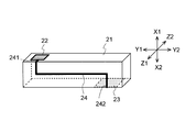
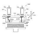
- FIG. 1 is a schematic diagram showing a configuration of a sensing device according to an embodiment of the present disclosure.
- FIG. 2 is a schematic perspective view of the structure according to the embodiment of the present disclosure.
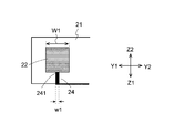
- FIG. 3 is an enlarged view showing a configuration in the vicinity of the first end portion of the wiring portion.
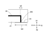
- FIG. 4 is an enlarged view showing a configuration in the vicinity of the second end portion of the wiring portion.
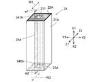
- FIG. 5 is a schematic perspective view showing a configuration of a structure included in the sensing device of the first modification.
- FIG. 6 is a schematic perspective view showing a configuration of a structure included in the sensing device of the second modification.
- FIG. 7 is a schematic cross-sectional view of the structure of the second modified example.
- FIG. 1 is a schematic diagram showing a configuration of a sensing device according to an embodiment of the present disclosure.
- FIG. 2 is a schematic perspective view of the structure according to the embodiment of the present disclosure.
- FIG. 3 is an enlarged view showing a configuration in
- FIG. 8 is a schematic perspective view showing the structure of the structure included in the sensing device of the third modification.
- FIG. 9 is a schematic cross-sectional view of the structure of the third modified example.
- FIG. 10 is a schematic perspective view showing the configuration of the sensing device of the fourth modification.
- FIG. 11 is a diagram for explaining a first use example of the sensing device of the fourth modification.
- FIG. 12A is a diagram for explaining a second use example of the sensing device of the fourth modification.
- FIG. 12B is a diagram for explaining a second use example of the sensing device of the fourth modification.
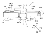
- FIG. 13 is a schematic perspective view showing a configuration of a structure included in the sensing device of the fifth modification.
- FIG. 14 is an exploded view of the periphery of the portion of the structure shown in FIG. 13 where the movable mechanism is provided.
- the X direction in which the detection electrode 11 and the first electrode portion 22 face each other is defined as the vertical direction.
- the Y direction which is one of the two directions orthogonal to each other on the plane orthogonal to the X direction, is the left-right direction
- the Z direction which is the other direction, is the front-back direction.
- the X1 side shown in the drawing is the upper side
- the X2 side is the lower side
- the Y1 side is the left side
- the Y2 side is the right side
- the Z1 side is the front side
- the Z2 side is the rear side.
- FIG. 1 is a schematic view showing the configuration of the sensing device 100 according to the embodiment of the present disclosure.
- FIG. 1 also shows a target 200 to be detected by the sensing device 100.
- the target 200 is, for example, an object (work) to be processed such as processing or inspection at a production site.
- the target 200 is, for example, an object gripped by a robot hand.
- the shape of the target 200 may be diverse.
- the sensing device 100 is a capacitance type sensing device.
- the sensing device 100 detects the approach of the target 200.
- the sensing device 100 includes a capacitance sensor 1 and a structure 2.
- the capacitance sensor 1 detects a change in capacitance.
- the capacitance sensor 1 has a detection electrode 11.
- the detection electrode 11 is made of a metal such as copper or a copper alloy.
- the detection electrode 11 has a plate shape or a thin film shape extending in a direction orthogonal to the vertical direction.
- the detection electrode 11 may have another shape such as a curved shape.
- the detection electrode 11 is an electrode for detecting a change in capacitance due to electrostatic induction occurring in a conductor portion of the structure 2.
- the capacitance sensor 1 further includes a case 12, a circuit unit 13, and a lead wire 14.
- the case 12 is made of, for example, resin, and houses the detection electrode 11 and the circuit unit 13. In this embodiment, the case 12 extends in the vertical direction.
- the detection electrode 11 is arranged at the lower end of the case 12. Therefore, the lower end surface of the case 12 becomes the detection surface of the capacitance sensor 1.
- An opening (not shown) is provided on the upper end surface of the case 12, so that the lead wire 14 can be pulled out to the outside of the case 12.
- the lead wire 14 includes, for example, a power line and a signal line.
- the circuit unit 13 is electrically connected to the detection electrode 11.
- the circuit unit 13 together with the detection electrode 11 constitutes a detection circuit for detecting a change in capacitance.
- the circuit unit 13 detects a change in capacitance by the detection circuit, the circuit unit 13 outputs a detection signal to the outside of the capacitance sensor 1 via the lead wire 14.
- the circuit unit 13 is composed of, for example, a printed circuit board having a circuit pattern formed of copper foil or the like. In the present embodiment, the printed circuit board constituting the circuit unit 13 is arranged above the detection electrode 11, and is electrically connected to the detection electrode 11 by a connection line (not shown).
- the structure 2 has a surface facing the detection electrode 11.
- the structure 2 has a surface facing the detection electrode 11 via the case 12.
- the structure 2 may have a surface that directly faces the detection electrode 11.
- the capacitance sensor 1 may be attached to the structure 2 or may be attached to an object different from the structure 2.
- the structure 2 has a base 21, a first electrode portion 22, a second electrode portion 23, and a wiring portion 24.
- the base 21 has an insulating property.
- the insulating base 21 is made of, for example, a resin.
- the base 21 is a main member constituting the structure 2.
- the shape of the base 21 may be diverse.
- the base 21 may be, for example, a columnar column such as a prismatic column or a columnar column. Further, the base 21 may have a shape in which a plurality of columnar portions are combined, and may be, for example, an L-shape or an S-shape. Further, the base 21 may be configured to partially include a movable mechanism.
- the base 21 may be, for example, a component constituting the robot hand.
- the first electrode portion 22 is made of an electric conductor, and is made of a metal such as copper or a copper alloy.
- the first electrode portion 22 is arranged at a position facing the detection electrode 11 of the base 21.
- the first electrode portion 22 is arranged vertically separated from the detection electrode 11.
- the first electrode portion 22 has a plate shape or a thin film shape that spreads in a direction orthogonal to the vertical direction.
- the first electrode portion 22 may have another shape such as a curved shape.
- the first electrode portion 22 and the detection electrode 11 may face each other with the same area, or may face one with a larger area of the other.
- the second electrode portion 23 is made of an electric conductor, and is made of a metal such as copper or a copper alloy.
- the second electrode portion 23 is arranged at a position away from the first electrode portion 22 of the base 21.
- the second electrode portion 23 is arranged at a position where it is desired to detect the approach of the target 200 to be detected.
- the second electrode portion 23 has a plate shape or a thin film shape that spreads in a direction orthogonal to the direction facing the target 200.
- the second electrode portion 23 may have another shape such as a curved shape.
- the second electrode portion 23 and the target 200 may face each other with the same area, or may face one with a larger area of the other.
- the first electrode portion 22 and the second electrode portion 23 are preferably arranged on the outer surface of the base 21. As a result, the distance between the detection electrode 11 and the first electrode portion 22 and the distance from the target 200 to the second electrode portion 23 can be shortened, so that the approach of the target 200 can be detected. Sensitivity can be improved.
- the first electrode portion 22 and the second electrode portion 23 may be arranged inside the base 21.
- the first electrode portion 22 and the second electrode portion 23 are preferably arranged near the outer surface of the base 21.
- the respective electrode portions 22 and 23 may be coated with a protective material for the purpose of improving durability and the like.
- the wiring portion 24 is made of an electric conductor, and is made of a metal such as copper or a copper alloy.
- the wiring portion 24 is arranged on the base 21.
- the wiring portion 24 may be arranged on the outer surface of the base 21 or may be arranged inside the base 21.
- the wiring portion 24 may be coated with a protective material for the purpose of improving durability or the like.
- the wiring portion 24 electrically connects the first electrode portion 22 and the second electrode portion 23.
- the wiring portion 24 is basically linear.
- the wiring portion 24 may have a thick wire shape or a thin wire shape.
- the line width of the wiring portion 24 may be constant, but may have a plurality of line widths.
- the wiring portion 24 may be composed of only a straight portion, but is not limited to this, and may have a configuration having a straight portion and a curved portion, or a configuration having only a curved portion.
- the wiring portion 24 may have a configuration in which, when the base 21 has a movable mechanism, a coupling electrode portion for keeping the capacitance constant regardless of the movement by the movable mechanism is provided between both ends. That is, the wiring portion 24 may have a non-linear portion.
- the sensing device 100 when the target 200 approaches the second electrode portion 23, electrostatic induction occurs in the conductor portion composed of the first electrode portion 22, the second electrode portion 23, and the wiring portion 24. .. As a result, the detection electrode 11 detects the change in capacitance. By detecting the change in capacitance by the detection electrode 11, the sensing device 100 detects the approach of the target 200.
- the target 200 can be detected by the second electrode portion 23 provided at a position away from the detection electrode 11 of the capacitance sensor 1. Therefore, the degree of freedom in designing the detection location of the target 200 can be improved.
- the second electrode portion 23 can be arranged so as to narrow down the target 200 to a region to be detected. Further, according to this configuration, since the electrode portions 22 and 23 are connected by the wiring portion 24, the surface area of the conductor of the structure 2 can be reduced. That is, according to this configuration, it is possible to suppress the change in capacitance due to an object approaching a position away from the position where the target 200 should be detected. Therefore, the approach of the target 200 can be appropriately detected.
- FIG. 2 is a schematic perspective view of the structure 2 according to the embodiment of the present disclosure.
- the base 21 has a rectangular parallelepiped shape extending in the left-right direction. That is, the base 21 has a plurality of surfaces. However, the base 21 may have a configuration having only one surface such as a spherical shape.
- the first electrode portion 22, the second electrode portion 23, and the wiring portion 24 are arranged on the outer surface of the base 21.
- the first electrode portion 22 and the second electrode portion 23 are arranged on different surfaces. According to this, the degree of freedom regarding the arrangement of the second electrode portion 23 for detecting the target 200 can be improved.
- the first electrode portion 22 is arranged on one of the four surfaces extending in the left-right direction. As an example, the first electrode portion 22 is arranged on the upper surface of the base 21.
- the second electrode portion 23 is arranged on the lower surface opposite to the surface on which the first electrode portion 22 is arranged.
- the second electrode portion 23 may be arranged on any one of four surfaces adjacent to the surface on which the first electrode portion 22 is arranged. Further, the first electrode portion 22 and the second electrode portion 23 may be arranged on the same surface.
- the second electrode portion 23 is arranged on one of the plurality of surfaces of the base 21. According to this, the range in which the second electrode portion 23 for detecting the target 200 is provided in the structure 2 can be narrowed down, and the surface area of the conductor provided in the structure 2 can be reduced. Therefore, it is possible to suppress the change in capacitance with the approach of an object other than the target 200, and it is possible to appropriately detect the approach of the target 200.
- the second electrode portion 23 may be arranged so as to straddle a plurality of surfaces of the base 21. For example, when the target 200 approaches in a plurality of directions, the second electrode portion 23 may be arranged across the plurality of surfaces. The second electrode portion 23 may be divided into a plurality of surfaces and arranged. Further, the first electrode portion 22 may also be arranged on a plurality of surfaces of the base 21.
- the wiring portion 24 has a first end portion 241 and a second end portion 242.
- the first end portion 241 is one end portion of the wiring portion 24.
- the second end portion 242 is the other end portion of the wiring portion 24.
- the first end 241 and the second end 242 are linear.
- the linear first end portion 241 extends from the first electrode portion 22.
- the linear second end portion 242 extends from the second electrode portion 23.
- the wiring portion 24 is linear as a whole, and the line width is constant.
- FIG. 3 is an enlarged view showing a configuration in the vicinity of the first end portion 241 of the wiring portion 24.
- FIG. 3 is a plan view of the upper surface including the first end portion 241 of the base 21 from above.
- the first electrode portion 22 has a rectangular shape.
- the first electrode portion 22 may have another shape such as a circular shape or an elliptical shape.
- the first end portion 241 extends from one side of the first electrode portion 22. Specifically, the first end portion 241 extends forward from the front side of the two sides parallel to the left and right directions of the first electrode portion 22. In the present embodiment, the first end portion 241 is arranged on the same surface of the first electrode portion 22 and the base 21. However, the first end portion 241 may be arranged on different surfaces of the first electrode portion 22 and the base 21.
- the width w1 of the first end portion 241 is narrower than the width W1 of the first electrode portion 22 in the same direction in a plan view toward the surface including the first end portion 241.
- the width w1 of the first end portion 241 is the line width of the linear first end portion 241.
- the linear first end portion 241 has a length in a direction extending from the first electrode portion 22 and a direction orthogonal to the direction in a plan view toward the surface including the first end portion 241.
- the width w1 of the first end portion 241 is the length of the latter.
- the first end portion 241 extends forward from the first electrode portion 22.
- the width w1 of the first end portion 241 is the length of the first end portion 241 in the left-right direction.
- FIG. 4 is an enlarged view showing a configuration in the vicinity of the second end portion 242 of the wiring portion 24.
- FIG. 4 is a plan view of the front surface including the second end portion 242 of the base 21 from the front side.
- the second electrode portion 23 has a rectangular shape.
- the second electrode portion 23 may have another shape such as a circular shape or an elliptical shape.
- the second end portion 242 extends from one side of the second electrode portion 23. Specifically, the second end portion 242 extends upward from the front side of the two sides parallel to the left and right directions of the second electrode portion 23. In the present embodiment, the second end portion 242 is arranged on a separate surface of the second electrode portion 23 and the base 21. The second end portion 242 is arranged on a surface adjacent to the surface on which the second electrode portion 23 is arranged. However, the second end portion 242 may be arranged on the same surface of the second electrode portion 23 and the base 21.
- the width w2 of the second end portion 242 is narrower than the width W2 of the second electrode portion 23 in the same direction.
- the width w2 of the second end portion 242 is the linear width of the second end portion 242.
- the linear second end portion 242 has a length in a direction extending from the second electrode portion 23 and a direction orthogonal to the direction in a plan view toward the surface including the second end portion 242.
- the width w2 of the second end 242 is the length of the latter.
- the second end portion 242 extends upward from the second electrode portion 23.
- the width w2 of the second end portion 242 is the length of the second end portion 242 in the left-right direction.
- the width W2 of the second electrode portion 23 in the same direction refers to the width in the same direction as the width w2 of the second end portion 242 of the second electrode portion 23.
- the width W2 of the second electrode portion 23 is the length of the second electrode portion 23 in the left-right direction. This is equal to the length of the side extending in the left-right direction of the second electrode portion 23.
- the width W2 of the second electrode portion 23 is equal to the diameter of the second electrode portion 23.
- the width of the wiring portion 24 is narrower than the width of the electrode portions 22 and 23 at least in the vicinity of the electrode portions 22 and 23, the surface area of the wiring portion 24 can be reduced and the wiring portion 24 approaches the wiring portion 24.
- the change in capacitance due to the object can be suppressed to a small value. That is, according to the present embodiment, the change in capacitance due to an object approaching a position away from the position where the target 200 should be detected can be suppressed to a small value, and the target 200 can be detected appropriately.
- the structure 2 configured as described above may be formed by, for example, a known MID (Molded Interconnect Device) method.
- a MID method a metal thin film is formed on the surface of a three-dimensional molded product formed by an injection molding method by sputtering or the like, and then the metal thin film is partially removed by laser processing to perform metal wiring on the surface of the three-dimensional molded product.
- the method of forming the above is exemplified.
- the structure 2 may be manufactured by a technique (AM-MID technique) in which a MID method and an additive manufacturing method (AM: Additive Manufacturing) are combined. That is, for the structure 2, the powder bed melt bonding method in the addition manufacturing method may be used instead of the injection molding method in the MID method.
- the powder bed fusion bonding method is a method in which powder materials are laminated layer by layer, the cross-sectional shape is melted by an energy source such as a laser or an electron beam, and then solidified to form a model.
- the metal complex added to the powder material can be activated by laser light to perform modeling, and the formation of metal wiring can be promoted while performing modeling.
- the structure 2 to which the metal wiring is applied can be obtained.
- the structure 2 by the AM-MID technique it is possible to freely form the wiring portion 24 having a predetermined shape not only on the surface of the structure 2 but also inside.
- FIG. 5 is a schematic perspective view showing the configuration of the structure 2A included in the sensing device of the first modification.
- the structure 2A has a rectangular parallelepiped base 21A extending in the vertical direction.
- the first electrode portion 22A facing the detection electrode 11 is provided on the upper surface of the base 21A.
- the first electrode portion 22A is provided on the entire upper surface of the base 21A. That is, the first electrode portion 22A has a rectangular shape.
- the second electrode portion 23A is provided on the lower surface of the base 21A.
- the second electrode portion 23A is provided on the entire lower surface of the base 21A. That is, the second electrode portion 23A is also rectangular.
- the first electrode portion 22A and the second electrode portion 23A may have a shape other than a rectangular shape, and may not be provided on the entire end face of the base 21.
- At least a part of the wiring portion 24A is arranged on the inner surface of the base 21A. According to this, since at least a part of the wiring portion 24A can be arranged at a position away from the outer surface of the base 21A, it is possible to suppress a small change in capacitance due to the influence of an object approaching the wiring portion 24A. Therefore, the approach of the target 200 can be appropriately detected. Further, according to this, it is possible to prevent foreign matter such as dust or moisture from adhering to the wiring portion 24A.
- the wiring portion 24A is arranged on the inner surface of the base 21A.
- the base 21A is provided with a through hole 211.
- the inner surface of the base 21A on which the wiring portion 24A is arranged is a surface forming the through hole 211.
- Such a configuration can be easily formed by AM-MID technology.
- the wiring portion 24A can be formed on the inner surface of the base 21A by eliminating the step of covering the wiring portion 24A with the insulating member. That is, the structure 2A of the present modification is easy to manufacture even though the wiring portion 24A is provided on the inner surface of the base 21A.
- the through hole 211 penetrates the base 21A in the vertical direction.
- the through hole 211 extends from the upper surface to the lower surface of the base 21A.
- the through hole 211 has a rectangular shape in a plan view from the vertical direction.
- the through hole 211 may have a shape other than a rectangular shape in a plan view from the vertical direction, and may have a circular shape, for example.
- the wiring portion 24A is formed on the entire surface of one of the four inner surfaces forming the through hole 211 of the base 21A. Specifically, the wiring portion 24A is formed on the surface located on the left side of the two inner surfaces orthogonal to the left-right direction. However, the wiring portion 24A may be formed on any of the four inner surfaces. Further, the wiring portion 24A may be formed over a plurality of four inner surfaces. Further, when the wiring portion 24A is formed on one inner surface, it may be formed on a part of the inner surface instead of the entire inner surface.
- the first end portion 241A of the wiring portion 24A extends downward from the first electrode portion 22A.
- the width w1 of the first end portion 241A is narrower than the width W1 of the first electrode portion 22A in the same direction in a plan view toward the surface including the first end portion 241A.
- the direction toward the surface including the first end portion 241A is a direction parallel to the left-right direction.
- the width w1 of the first end portion 241A is equal to the width of the through hole 211 in the front-rear direction.
- the width W1 of the first electrode portion 22A is equal to the width of the base 21A in the front-rear direction.
- the second end portion 242A of the wiring portion 24A extends upward from the second electrode portion 23A.
- the width w2 of the second end portion 242A is narrower than the width W2 of the second electrode portion 23A in the same direction in a plan view toward the surface including the second end portion 242A.
- the direction toward the surface including the second end portion 242A is a direction parallel to the left-right direction.
- the width w2 of the second end portion 242A is equal to the width of the through hole 211 in the front-rear direction.
- the width W2 of the second electrode portion 23A is equal to the width of the base 21A in the front-rear direction.
- the surface area of the wiring portion 24A can be reduced to keep the change in capacitance due to an object approaching the wiring portion 24A small. Further, in this modification, since the wiring portion 24A is arranged inside the base 21A, the change in capacitance due to an object approaching the wiring portion 24A can be further suppressed. That is, according to this modification, the target 200 can be detected more accurately.
- the structure 2 of this modification is suitable for manufacturing by AM-MID technology.
- the MID method using an injection molding method it is necessary to irradiate the inside of the base 21A with a laser beam in order to form the wiring portion 24A, which increases the difficulty of forming the wiring portion 24A.
- the AM-MID technology is used, the irradiation of the laser beam for forming the wiring portion 24A can be performed while performing the modeling, and the wiring portion 24A can be obtained only by performing the plating treatment after the modeling is completed. In addition, the wiring portion 24A can be easily formed.
- an insulating material may be inserted into the through hole 211 to fill the through hole 211. With this configuration, it is possible to prevent foreign matter such as moisture from adhering to the wiring portion 24A.
- FIG. 6 is a schematic perspective view showing the configuration of the structure 2B included in the sensing device of the second modification.
- the structure 2B has a rectangular parallelepiped base 21B extending in the left-right direction.
- the structure 2B has a first electrode portion 22B provided on the upper surface of the base 21B and a second electrode portion 23B provided on the lower surface of the base 21B, as in the first modification.
- the structure 2B has two through holes 211Ba and 211Bb that penetrate in the vertical direction, similarly to the through holes 211 of the first modification.
- the first through hole 211Ba and the second through hole 211Bb are arranged at intervals in the left-right direction.
- the first through hole 211Ba is arranged on the left side with respect to the second through hole 211Bb.
- the first wiring portion 24Ba is formed on one of the four inner surfaces constituting the first through hole 211Ba. Specifically, the first wiring portion 24Ba is formed on the inner surface on the right side of the two inner surfaces orthogonal to the left-right direction.
- a second wiring portion 24Bb is formed on one of the four inner surfaces constituting the second through hole 211Bb. Specifically, the second wiring portion 24Bb is formed on the inner surface on the left side of the two inner surfaces orthogonal to the left-right direction.
- the first end portion 241Ba of the first wiring portion 24Ba is connected to the first electrode portion 22B.
- the second end portion 242Ba of the first wiring portion 24Ba is connected to the second electrode portion 23B.
- the first end portion 241Bb of the second wiring portion 24Bb is connected to the first electrode portion 22B.
- the second end portion 242Bb of the second wiring portion 24Bb is connected to the second electrode portion 23B.
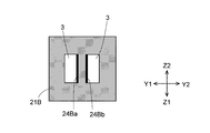
- the structure 2B has a low dielectric constant layer 3 having a dielectric constant lower than that of the base 21B between the outer surface of the base 21B and the wiring portion 24B.
- the change in capacitance due to an object approaching the outer surface of the base 21B is smaller than that in the case where the space between the outer surface of the base 21B and the wiring portion 24B is filled with the material constituting the base 21B. It can be suppressed. This will be described in detail with reference to FIG.
- the low dielectric constant layer 3 is in contact with the wiring portion 24B.
- FIG. 7 is a schematic cross-sectional view of the structure 2B of the second modification.
- FIG. 7 is a cross-sectional view of the structure 2B of the second modified example cut in a direction orthogonal to the vertical direction.
- the base 21B has a low dielectric constant layer 3 facing the first wiring portion 24Ba between the left outer surface of the base 21B and the first wiring portion 24Ba.
- the low dielectric constant layer 3 is an air layer.
- the left side of the base 21B is compared with the case where only the resin material constituting the base 21B is arranged between the outer surface on the left side of the base 21B and the first wiring portion 24Ba. It is possible to reduce the change in capacitance that occurs when an object approaches the outer surface of the side.
- the base 21B also has an air layer 3 facing the second wiring portion 24Bb between the outer surface on the right side of the base 21B and the second wiring portion 24Bb. Therefore, in this modification, the right side of the base 21B is compared with the case where only the resin material constituting the base 21B is arranged between the outer surface on the right side of the base 21B and the second wiring portion 24Bb. It is possible to reduce the change in capacitance that occurs when an object approaches the outer surface of the side.
- the change in capacitance due to an object approaching the left and right outer surfaces of the base 21B can be suppressed to a small extent, so that the approach of the target 200 can be appropriately detected.
- the right side of the wiring portion 24A faces the air layer.
- the left side of the wiring portion 24A is configured not to face the air layer. For this reason, in the configuration of the first modification, the change in capacitance due to the approach of an object tends to be larger on the left side than on the right side.
- the structure 2B of this modified example is also more suitable for manufacturing by the AM-MID technique than the MID method using the injection molding method.
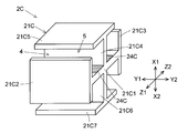
- FIG. 8 is a schematic perspective view showing the configuration of the structure 2C included in the sensing device of the third modification.
- FIG. 8 shows a part of the structure 2C.
- the structure 2C extends in the left-right direction.
- the structure 2C has a base 21C formed by combining a plurality of rectangular parallelepiped flat plate portions 21C1 to 21C7.
- the first flat plate portion 21C1 extends in a direction orthogonal to the vertical direction and extends in the horizontal direction.
- the second flat plate portion 21C2 is connected to the front end portion of the first flat plate portion 21C1.
- the second flat plate portion 21C2 extends in a direction orthogonal to the front-rear direction and extends in the left-right direction.
- the third flat plate portion 21C3 is connected to the rear end portion of the first flat plate portion 21C1.
- the third flat plate portion 21C3 extends in a direction orthogonal to the front-rear direction and extends in the left-right direction.
- the fourth flat plate portion 21C4 extends upward from the central portion in the front-rear direction of the first flat plate portion 21C1.
- the fifth flat plate portion 21C5 is connected to the upper end portion of the fourth flat plate portion 21C4.
- the fifth flat plate portion 21C5 extends in a direction orthogonal to the vertical direction and extends in the horizontal direction.
- the sixth flat plate portion 21C6 extends downward from the central portion in the front-rear direction of the first flat plate portion 21C1.
- the seventh flat plate portion 21C7 is connected to the lower end portion of the sixth flat plate portion 21C6.
- the seventh flat plate portion 21C7 extends in a direction orthogonal to the vertical direction and extends in the horizontal direction.
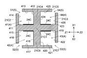
- FIG. 9 is a schematic cross-sectional view of the structure 2C of the third modification.
- FIG. 9 is a cross-sectional view of the structure 2C cut in a direction orthogonal to the left-right direction.
- the base 21C is provided with an internal space 4 having an opening 5 in a cross-sectional view extending in a specific direction and having a cross section orthogonal to the specific direction.
- the specific direction is the left-right direction.
- Four internal spaces 4 are provided.
- the first internal space 41 is composed of a first inner surface 411, a second inner surface 412, a third inner surface 413, and a fourth inner surface 414.
- the first inner surface 411 is an upper surface of the first flat plate portion 21C1 and a surface located in front of the fourth flat plate portion 21C4.
- the second inner surface 412 is the front surface of the fourth flat plate portion 21C4.
- the third inner surface 413 is a surface located on the lower surface of the fifth flat plate portion 21C5 and in front of the fourth flat plate portion 21C4.
- the fourth inner surface 414 is a rear surface of the second flat plate portion 21C2 and a surface located above the first flat plate portion 21C1.
- the first inner surface 411 and the second inner surface 412 are connected to each other.
- the second inner surface 412 and the third inner surface 413 are connected to each other.
- the third inner surface 413 and the fourth inner surface 414 are not connected to each other, and a first opening 51 is formed between them.
- the fourth inner surface 414 and the first inner surface 411 are connected to each other.
- the second internal space 42 is composed of a fifth inner surface 415, a sixth inner surface 416, a seventh inner surface 417, and an eighth inner surface 418.
- the fifth inner surface 415 is a lower surface of the first flat plate portion 21C1 and a surface located in front of the sixth flat plate portion 21C6.
- the sixth inner surface 416 is a front surface of the sixth flat plate portion 21C6.
- the seventh inner surface 417 is an upper surface of the seventh flat plate portion 21C7 and a surface located in front of the sixth flat plate portion 21C6.
- the eighth inner surface 418 is a rear surface of the second flat plate portion 21C2 and a surface located below the first flat plate portion 21C1.
- the fifth inner surface 415 and the sixth inner surface 416 are connected to each other.
- the sixth inner surface 416 and the seventh inner surface 417 are connected to each other.
- the seventh inner surface 417 and the eighth inner surface 418 are not connected to each other, and a second opening 52 is formed between them.
- the eighth inner surface 418 and the fifth inner surface 415 are connected to each other.
- the third interior space 43 is composed of a ninth inner surface 419, a tenth inner surface 420, an eleventh inner surface 421, and a twelfth inner surface 422.
- the ninth inner surface 419 is a lower surface of the first flat plate portion 21C1 and a surface located behind the sixth flat plate portion 21C6.
- the tenth inner surface 420 is the rear surface of the sixth flat plate portion 21C6.
- the eleventh inner surface 421 is a surface located on the upper surface of the seventh flat plate portion 21C7 and behind the sixth flat plate portion 21C6.
- the twelfth inner surface 422 is a surface located on the front surface of the third flat plate portion 21C3 and below the first flat plate portion 21C1.
- the 9th inner surface 419 and the 10th inner surface 420 are connected to each other.
- the 10th inner surface 420 and the 11th inner surface 421 are connected to each other.
- the eleventh inner surface 421 and the twelfth inner surface 422 are not connected to each other, and a third opening 53 is formed between the two.
- the twelfth inner surface 422 and the ninth inner surface 419 are connected to each other.
- the fourth interior space 44 is composed of a thirteenth inner surface 423, a fourteenth inner surface 424, a fifteenth inner surface 425, and a sixteenth inner surface 426.
- the thirteenth inner surface 423 is an upper surface of the first flat plate portion 21C1 and a surface located behind the fourth flat plate portion 21C4.
- the 14th inner surface 424 is the rear surface of the 4th flat plate portion 21C4.
- the fifteenth inner surface 425 is a lower surface of the fifth flat plate portion 21C5 and a surface located behind the fourth flat plate portion 21C4.
- the 16th inner surface 426 is a surface located on the front surface of the third flat plate portion 21C3 and above the first flat plate portion 21C1.
- the 13th inner surface 423 and the 14th inner surface 424 are connected to each other.
- the 14th inner surface 424 and the 15th inner surface 425 are connected to each other.
- the 15th inner surface 425 and the 16th inner surface 426 are not connected to each other, and a fourth opening 54 is formed between the two.
- the 16th inner surface 426 and the 13th inner surface 423 are connected to each other.
- the wiring portion 24C is arranged on the first inner surface 411, the fifth inner surface 415, the ninth inner surface 419, and the thirteenth inner surface 423.
- the number of wiring portions 24C is not limited to four, and may be a single number or a plurality of wiring portions 24C other than four.
- the inner surfaces 411, 415, 419, and 423 of the base 21 on which the wiring portion 24C is arranged are the surfaces forming the internal spaces 41 to 44 of the base 21C. According to this, since the wiring portion 24C can be arranged at a position away from the outer surface of the base 21C, it is possible to suppress a small change in capacitance due to the influence of an object approaching the wiring portion 24C.
- the wiring portion 24C can be arranged not only in the closed internal space but also in the internal space having an opening in a part thereof.
- the wiring portion 24C may be provided on the entire surface of each inner surface 411, 415, 419, 423, but is preferably provided on a part of the inner surface. Further, in each of the internal spaces 41 to 44, the surface on which the wiring portion 24C is provided may be different from the surface described above. Further, the wiring portion 24C may be formed so as to straddle a plurality of inner surfaces. Further, also in this modification, the width of the first end portion (not shown) of the wiring portion 24C is the same direction as that of the first electrode portion (not shown) in a plan view toward the surface including the first end portion. Narrower than the width.
- the width of the second end portion (not shown) of the wiring portion 24C is narrower than the width of the second electrode portion (not shown) in the same direction in a plan view toward the surface including the second end portion. That is, the surface area of the wiring portion 24C can be reduced, and the change in capacitance due to an object approaching the wiring portion 24C can be suppressed to be small.
- FIG. 10 is a schematic perspective view showing the configuration of the sensing device 100D of the fourth modification.
- the sensing device 100D has two capacitance sensors 1Da and 1Db.
- the first capacitance sensor 1Da and the second capacitance sensor 1Db have the same configuration, and have the same configuration as the capacitance sensor 1 of the above-described embodiment.
- the structure 2D included in the sensing device 100D has a rectangular parallelepiped base 21D extending in the left-right direction.
- the two capacitance sensors 1Da and 1Db are arranged in the left-right direction and face the upper surface of the base 21D in the vertical direction.
- the first capacitance sensor 1Da is arranged on the left side of the second capacitance sensor 1Db.
- Two first electrode portions 22Da and 22Db which are arranged at intervals in the left-right direction, are arranged on the upper surface of the base 21D.
- One of the two first electrode portions 22Da and 22Db, the first electrode portion 22Da is arranged at a position facing the detection electrode 11Da of the first capacitance sensor 1Da.
- the other first electrode portion 22Db of the two first electrode portions 22Da and 22Db is arranged at a position facing the detection electrode 11Db of the second capacitance sensor 1Db.
- the shapes of the two first electrode portions 22Da and 22Db are the same as those of the first electrode portion 22 of the above-described embodiment.
- Two second electrode portions 23Da and 23Db which are arranged at intervals in the left-right direction, are arranged on the lower surface of the base 21D.
- the second electrode portion 23Da arranged on the left side of the two second electrode portions 23Da and 23Db includes the first electrode portion 22Da arranged on the left side of the two first electrode portions 22Da and 22Db. It is connected by the wiring unit 24Da.
- the second electrode portion 23Db arranged on the right side of the two second electrode portions 23Da and 23Db includes the first electrode portion 22Db arranged on the right side of the two first electrode portions 22Da and 22Db. It is electrically connected by the wiring portion 24Db.
- the shapes of the two second electrode portions 23Da and 23Db are the same as those of the second electrode portion 23 of the above-described embodiment.
- both of the two wiring portions 24Da and 24Db are in the form of fine wires as a preferable form. That is, in a plan view toward the surface including the first end portions 241Da and 241Db, the width of the first end portions 241Da and 241Db is narrower than the width of the first electrode portions 22Da and 22Db in the same direction. The width of the second end portions 242Da and 242Db is narrower than the width of the second electrode portions 23Da and 23Db in the same direction in a plan view toward the surface including the second end portions 242Da and 242Db. As a result, it is possible to suppress a change in capacitance when an object approaches the wiring portions 24Da and 24Db, and it is possible to appropriately detect the approach of the target to the second electrode portions 23Da and 23Db.
- the structure 2D has a plurality of sets of the capacitance sensors 1Da and 1Db, the first electrode portions 22Da and 22Db, the second electrode portions 23Da and 23Db, and the wiring portions 24Da and 24Db. ..
- the number of pairs is two. However, the number of pairs may be three or more.
- the set composed of the capacitance sensor 1Da, the first electrode section 22Da, the second electrode section 23Da, and the wiring section 24Da is referred to as the first set Gr1.
- the set composed of the capacitance sensor 1Db, the first electrode section 22Db, the second electrode section 23Db, and the wiring section 24Db is referred to as the second set Gr2. According to this modification, it is possible to separately detect a plurality of targets 200 approaching different positions of the structure 2D. Further, according to the present modification, it is possible to distinguish and detect a plurality of types of targets 200 approaching the structure 2D.
- the two first electrode portions 22Da and 22Db may be arranged on different surfaces of the base 21D. Further, the two second electrode portions 23Da and 23Db may be arranged on different surfaces of the base 21D.
- the arrangement and shape of the wiring portions 24Da and 24Db may be changed according to the arrangement of the first electrode portions 22Da and 22Db and the second electrode portions 23Da and 23Db.
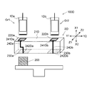
- FIG. 11 is a diagram for explaining a first use example of the sensing device 100D of the fourth modification.
- the first use example it is assumed that different targets 201 and 202 approach two predetermined positions of the structure 2D.
- the approach of the first target 201 to the left side of the lower surface of the structure 2D is detected.
- the approach of the second target 202 to the right side of the lower surface of the structure 2D is detected.
- the first target 201 approaches to the left of the lower surface of the structure 2D and the second target to the right of the lower surface of the structure 2D.
- the approach of 202 can be detected at the same time.
- the type of the first target 201 and the second target 202 does not matter.
- the first target 201 may be a human hand
- the second target 202 may be a work to be processed by the robot.
- 12A and 12B are diagrams for explaining a second use example of the sensing device 100D of the fourth modification.
- the second use example it is assumed that two targets 203 and 204 having different lengths in the left-right direction approach the structure 2D at different timings.
- FIG. 13 is a schematic perspective view showing the configuration of the structure 2E included in the sensing device of the fifth modification. At least a part of the structure 2E is movably provided with respect to the detection electrode 11 included in the capacitance sensor 1. According to this, since the position where the target 200 is detected can be changed without moving the capacitance sensor 1, the degree of freedom in designing the sensing device for detecting the target 200 can be improved. In this modification, a part of the structure 2E is movably provided with respect to the detection electrode 11.
- the base 21E is composed of a plurality of base members.
- the structure 2E has at least one movable mechanism 20 between the first electrode portion 22E and the second electrode portion 23E that allows the other member to move with respect to one member.
- the base 21E has two base members 21E1 and 21E2.
- the number of movable mechanisms 20 included in the structure 2E is one.
- the movable mechanism 20 makes the second base member 21E2 movable with respect to the first base member 21E1.
- FIG. 14 is an exploded view of the periphery of the portion of the structure 2E shown in FIG. 13 where the movable mechanism 20 is provided.
- the first base member 21E1 has a main body portion 21E11, a first connecting portion 21E12, and a second connecting portion 21E13.
- the main body portion 21E11, the first connecting portion 21E12, and the second connecting portion 21E13 are prepared separately and integrated in the middle of manufacturing to form the first base member 21E1.
- the main body portion 21E11 and the first connecting portion 21E12 may be formed by the AM-MID technique including a part of the first electrode portion 22E and the wiring portion 24E, respectively.
- the main body portion 21E11 and the first connecting portion 21E12, or the main body portion 21E11 and the second connecting portion 21E13 may be integrally formed by AM-MID technology.
- the main body 21E11 is a prismatic shape extending in the left-right direction.
- the first connecting portion 21E12 has a plate shape extending in the left-right direction, and is arranged on the right side of the main body portion 21E11.
- the first connecting portion 21E12 has a connecting portion recess 21E12a that is recessed upward on the right side of the lower surface.
- the connecting portion recess 21E12a has a circular shape in a plan view from the vertical direction.
- the second connecting portion 21E13 has a plate shape extending in the left-right direction, and is arranged on the right side of the main body portion 21E11.
- the second connecting portion 21E13 has a connecting portion convex portion 21E13a projecting upward on the right side of the upper surface.
- the convex portion 21E13a of the connecting portion is a columnar shape extending in the vertical direction.
- a part of the first connecting portion 21E12 is overlapped with the right end portion of the upper surface of the main body portion 21E11 and fixed to the main body portion 21E11.
- the connecting portion recess 21E12a is arranged on the right side of the right end of the main body portion 21E11 and is exposed without being covered by the main body portion 21E11.
- a part of the second connecting portion 21E13 is overlapped with the right end portion of the lower surface of the main body portion 21E11 and fixed to the main body portion 21E11.
- the connecting portion convex portion 21E13a is arranged on the right side of the right end of the main body portion 21E11 and does not overlap with the main body portion 21E11.
- the circular connecting portion concave portion 21E12a and the columnar connecting portion convex portion 21E13a are arranged in the vertical direction with the same center position.
- the upper part of the connecting portion convex portion 21E13a is inserted into the connecting portion concave portion 21E12a.
- the main body portion 21E11 and the connecting portions 21E12 and 21E13 may be fixed by, for example, an adhesive or a screw.
- a fixing method other than fixing with an adhesive or a screw may be used.
- the second base member 21E2 has a prismatic portion 21E21 and a tubular portion 21E22.
- the prismatic portion 21E21 and the tubular portion 21E22 are single members.
- the prism portion 21E21 is a square pillar extending in the left-right direction.
- the tubular portion 21E22 has a cylindrical shape extending in the vertical direction.
- the tubular portion 21E22 is arranged on the left side of the prismatic portion 21E21.
- the tubular portion 21E22 is arranged with a gap on the right side of the main body portion 21E11.
- the convex portion 21E13a of the connecting portion is inserted into the hole 21E22a extending in the vertical direction of the tubular portion 21E22.
- the second base member 21E2 is rotatably supported by the first base member 21E1 about the central axis C.
- the structure 2E may have a drive unit (not shown) that rotates the second base member 21E2 with respect to the first base member 21E1.
- the drive unit may be, for example, a motor or the like.
- the right end portion of the second base member 21E2 can be moved in the front-rear direction by rotation.
- the first connecting portion 21E12, the second connecting portion 21E13, and the tubular portion 21E22 form a movable mechanism 20.
- the movable mechanism 20 is a rotating mechanism.
- the movable mechanism 20 makes the other member 21E2 rotatable with respect to one member 21E1.
- the movable mechanism may have a configuration that allows the other member to move linearly with respect to one member. That is, the movable mechanism may be a linear motion mechanism.
- a first electrode portion 22E is provided on the upper surface of the main body portion 21E11. That is, the first base member 21E1 has a first electrode portion 22E.
- the first electrode portion 22E is a circular thin film, and is arranged at the left end portion of the main body portion 21E11.
- the first electrode portion 22E may have another shape such as a rectangular shape.
- a second electrode portion 23E is provided on the front surface of the prism portion 21E21. That is, the second base member 21E2 has a second electrode portion 23E.
- the second electrode portion 23E is a rectangular thin film, and is arranged at the right end portion of the prism portion 21E21.
- the second electrode portion 23E may have another shape such as a circular shape.
- the wiring portion 24E includes a first coupling electrode portion 24E1 included in the first base member 21E1 and a second coupling electrode portion 24E2 included in the second base member 21E2.
- the wiring portion 24E has a first coupling electrode portion 24E1 included in one member 21E1 and a second coupling electrode portion 24E2 included in the other member 21E2.
- the wiring portion 24E has a linear portion 24E3 in addition to the first coupling electrode portion 24E1 and the second coupling electrode portion 24E2.
- the wiring portion 24E including the first coupling electrode portion 24E1 and the second coupling electrode portion 24E2 is composed of a thin film.
- the upper surface of the main body 21E11 has a linear portion 24E3 extending from the first electrode portion 22E to the right end of the main body 21E11.
- a linear portion 24E3 and a first coupling electrode portion 24E1 are provided on the lower surface of the first connecting portion 21E12.
- the first coupling electrode portion 24E1 is an annular electrode centered on the central axis C.
- the first coupling electrode portion 24E1 surrounds the connecting portion recess 21E12a.
- the linear portion 24E3 provided in the first connecting portion 21E12 extends from the left end of the first connecting portion 21E12 to the first coupling electrode portion 24E1.
- the linear portion 24E3 provided in the first connecting portion 21E12 overlaps in a state of being in contact with the linear portion 24E3 provided in the main body portion 21E11.
- a second coupling electrode portion 24E2 is provided on the upper surface of the second base member 21E2.
- the second coupling electrode portion 24E2 surrounds the hole 21E22a of the tubular portion 21E22 and has an annular shape centered on the central axis C.
- the second base member 21E2 is provided with a linear portion 24E3 that connects the second coupling electrode portion 24E2 and the second electrode portion 23E.
- the second coupling electrode portion 24E2 is an annular electrode that faces the first coupling electrode portion 24E1 with a certain gap in the direction in which the central axis C extends.
- the first coupling electrode portion 24E1 and the second coupling electrode portion 24E2 are congruent. However, the two do not have to be joint.
- the area and gap of the second coupling electrode portion 24E2 facing the first coupling electrode portion 24E1 do not change when the second base member 21E2 moves with respect to the first base member 21E1.
- the second coupling electrode portion 24E2 keeps the capacitance between the second coupling electrode portion 24E2 and the first coupling electrode portion 24E1 constant regardless of the movement of the movable mechanism 20. Therefore, even when the movable mechanism 20 is present between the first electrode portion 22E and the second electrode portion 23E of the structure 2E, the first electrode portion 22E is not affected by the movement of the movable mechanism 20. , The capacitance between the conductor composed of the second electrode portion 23E and the wiring portion 24E and the detection electrode 11 can be kept constant. That is, even if the movable mechanism 20 is provided between the first electrode portion 22E and the second electrode portion 23E, the target can be stably detected using the second electrode portion 23E.
- the first end portion 241E of the wiring portion 24E extends from the first electrode portion 22A toward the right.
- the width of the first end portion 241E is narrower than the width of the first electrode portion 22E in the same direction.
- the direction toward the surface including the first end portion 241E is a direction parallel to the vertical direction.
- the first end portion 241E is linear, and the width of the first end portion 241E in the front-rear direction is equal to the line width.
- the width of the first electrode portion 22E is equal to the diameter of the circular first electrode portion 22E.
- the second end portion 242E of the wiring portion 24E extends upward from the second electrode portion 23E.
- the width of the second end portion 242E is narrower than the width of the second electrode portion 23E in the same direction.
- the direction toward the surface including the second end portion 242E is a direction parallel to the front-rear direction.
- the second end portion 242E is linear, and the width of the second end portion 242E in the left-right direction is equal to the line width.
- the width of the second electrode portion 23E is equal to the width of the rectangular second electrode portion 23E in the left-right direction.
- the surface area of the wiring portion 24E can be reduced as much as possible, and the change in capacitance due to an object approaching the wiring portion 24E can be suppressed to be small. That is, according to this modification, the target 200 can be detected accurately.
- the present disclosure can be used, for example, for industrial robots.
Landscapes
- Engineering & Computer Science (AREA)
- Robotics (AREA)
- Mechanical Engineering (AREA)
- Switches That Are Operated By Magnetic Or Electric Fields (AREA)
Abstract
静電容量型のセンシング装置は、検出電極を有する静電容量センサと、前記検出電極と対向する面を有する構造体と、を有する。前記構造体は、絶縁性を有するベースと、前記ベースの前記検出電極と対向する位置に配置される第1電極部と、前記ベースの前記第1電極部から離れた位置に配置される第2電極部と、前記ベースに配置され、前記第1電極部と前記第2電極部とを電気的に接続する配線部と、を有する。
Description
本開示は、センシング装置に関する。
従来、作業内容に応じた適切なハンド(エンドエフェクタ)をアームの先端に装着し、ハンドで把持したワークをアームの駆動により移送する産業用ロボットが知られる。ロボットハンドには、形状又は姿勢等が異なる多様なワークそれぞれの情報を取得できるセンサが搭載される。このようなセンサの一例として、ワークの接近に伴う静電容量の変化を検出する静電容量型の近接センサが知られる。
静電容量の変化を検出する静電検出装置が知られている(例えば、日本国公開公報特開2018-37352号公報)。この静電検出装置は、車両の固定部に設定された静電検出用の電極と、可動部である窓ガラスに設定され、該電極とは独立した導電体とを備えている。帯電物によるターゲットが導電体に接近すると、導電体の帯電物に近い側には帯電物の電荷と反対符号の電荷が現れ、導電体の帯電物から遠い側には帯電物の電荷と同符号の電荷が現れる現象が起こる。こうした現象は静電誘導と呼ばれる。電極は、導電体に生じる静電誘導に伴う静電容量の変化を直接検出しつつ、ターゲットを間接的に検出する。
日本国公開公報特開2018-37352号公報の静電検出装置によれば、導電体に比べて小さい電極が導電体から間接的に影響を受けるために、フロアノイズを小さくできる。また、この静電検出装置は、独立した導電体が電波をカットするため、外来ノイズに対して強いとされる。
ロボットハンドの周辺には、多くの部材が存在することが想定される。また、日本国公開公報特開2018-37352号公報の静電検出装置においては、ターゲットを検出するための導電体が占める面積が大きくなり易い。このために、日本国公開公報特開2018-37352号公報の静電検出装置がロボットハンドに搭載された場合、検出すべきワーク以外の物体によって導電体の静電誘導が生じる可能性が高くなり、検出対象のワークを適切に検出できない可能性がある。
本開示は、検出すべき対象を適切に検出することができるセンシング技術を提供することを目的とする。
本開示の例示的なセンシング装置は、静電容量型のセンシング装置であって、検出電極を有する静電容量センサと、前記検出電極と対向する面を有する構造体と、を有する。前記構造体は、絶縁性を有するベースと、前記ベースの前記検出電極と対向する位置に配置される第1電極部と、前記ベースの前記第1電極部から離れた位置に配置される第2電極部と、前記ベースに配置され、前記第1電極部と前記第2電極部とを電気的に接続する配線部と、を有する。
例示的な本開示のセンシング装置によれば、検出すべき対象を適切に検出することができる。
以下、本開示の例示的な実施形態について、図面を参照しながら詳細に説明する。本明細書では、センシング装置100の説明において、検出電極11と第1電極部22とが互いに向き合うX方向を上下方向とする。また、X方向と直交する平面上において互いに直交する2つの方向のうちの一方であるY方向を左右方向とし、他方であるZ方向を前後方向とする。図面中に示されるX1側を上側、X2側を下側、Y1側を左側、Y2側を右側、Z1側を前側、Z2側を後側とする。これらの方向は単に説明のために用いられる名称であって、実際の位置関係及び方向を限定する意図はない。
<1.センシング装置の概要>
図1は、本開示の実施形態に係るセンシング装置100の構成を示す模式図である。図1には、センシング装置100の他に、センシング装置100によって検出すべき対象であるターゲット200も示されている。ターゲット200は、例えば、生産現場において加工又は検査等の処理の対象となる物体(ワーク)である。ターゲット200は、例えばロボットハンドによって把持される物体である。ターゲット200の形状は、多種多様であってよい。
図1は、本開示の実施形態に係るセンシング装置100の構成を示す模式図である。図1には、センシング装置100の他に、センシング装置100によって検出すべき対象であるターゲット200も示されている。ターゲット200は、例えば、生産現場において加工又は検査等の処理の対象となる物体(ワーク)である。ターゲット200は、例えばロボットハンドによって把持される物体である。ターゲット200の形状は、多種多様であってよい。
センシング装置100は、静電容量型のセンシング装置である。センシング装置100は、ターゲット200の接近を検出する。図1に示すように、センシング装置100は、静電容量センサ1と、構造体2とを有する。
静電容量センサ1は、静電容量の変化を検出する。静電容量センサ1は、検出電極11を有する。検出電極11は、例えば銅又は銅合金等の金属により構成される。本実施形態では、検出電極11は、上下方向に直交する方向に広がる板状又は薄膜状である。ただし、検出電極11は、湾曲形状等の他の形状であってもよい。検出電極11は、構造体2が有する導体部分に生じる静電誘導に伴う静電容量の変化を検出するための電極である。
静電容量センサ1は、ケース12と、回路部13と、リード線14とを更に有する。ケース12は、例えば樹脂で構成され、検出電極11および回路部13を収容する。本実施形態では、ケース12は上下方向に延びる。検出電極11は、ケース12の下端部に配置される。このために、ケース12の下端面が、静電容量センサ1の検出面になる。ケース12の上端面には、不図示の開口が設けられており、リード線14がケース12の外部に引き出し可能になっている。リード線14には、例えば電源線および信号線が含まれる。
回路部13は、検出電極11と電気的に接続される。回路部13は、検出電極11とともに、静電容量の変化を検出する検出回路を構成する。回路部13は、検出回路により静電容量の変化を検出すると、リード線14を介して検出信号を静電容量センサ1の外部に出力する。回路部13は、例えば、銅箔等で回路パターンが形成されたプリント基板により構成される。本実施形態では、回路部13を構成するプリント基板は、検出電極11に対して上側に配置され、不図示の接続線により検出電極11と電気的に接続される。
構造体2は、検出電極11と対向する面を有する。本実施形態では、構造体2は、ケース12を介して検出電極11と対向する面を有する。ただし、構造体2は、検出電極11と直接対向する面を有してもよい。なお、静電容量センサ1は、構造体2に取り付けられてもよいし、構造体2とは別の物体に取り付けられてもよい。図1に示すように、構造体2は、ベース21と、第1電極部22と、第2電極部23と、配線部24とを有する。
ベース21は、絶縁性を有する。絶縁性のベース21は、例えば樹脂により構成される。ベース21は、構造体2を構成する主要部材である。ベース21の形状は、多種多様であってよい。ベース21は、例えば、角柱状、円柱状等の柱状であってよい。また、ベース21は、複数の柱状部を組み合わせた形状であってよく、例えばL字状やS字状等であってよい。また、ベース21は、一部に可動機構を含んだ構成であってもよい。ベース21は、例えば、ロボットハンドを構成する構成要素であってよい。
第1電極部22は、電気伝導体で構成され、例えば銅又は銅合金等の金属で構成される。第1電極部22は、ベース21の検出電極11と対向する位置に配置される。第1電極部22は、検出電極11と上下方向に離間して配置される。第1電極部22は、上下方向と直交する方向に広がる板状又は薄膜状である。ただし、第1電極部22は、湾曲形状等の他の形状であってもよい。第1電極部22と検出電極11とは、面積を同じくして対向してもよいし、一方に対して他方の面積を大きくして対向してもよい。
第2電極部23は、電気伝導体で構成され、例えば銅又は銅合金等の金属で構成される。第2電極部23は、ベース21の第1電極部22から離れた位置に配置される。第2電極部23は、検出対象となるターゲット200の接近を検出したい位置に配置にされる。第2電極部23は、ターゲット200との対向方向と直交する方向に広がる板状又は薄膜状である。ただし、第2電極部23は、湾曲形状等の他の形状であってもよい。第2電極部23とターゲット200とは、面積を同じくして対向してもよいし、一方に対して他方の面積を大きくして対向してもよい。
第1電極部22および第2電極部23は、ベース21の外面に配置されることが好ましい。これにより、検出電極11と第1電極部22との間の距離、および、ターゲット200から第2電極部23までの距離とをそれぞれ短くすることができるために、ターゲット200の接近を検出するための感度を向上することができる。
なお、第1電極部22および第2電極部23は、ベース21の内部に配置されてもよい。この場合には、第1電極部22および第2電極部23は、ベース21の外面近傍に配置されることが好ましい。また、第1電極部22および第2電極部23がベース21の外面に配置される場合において、各電極部22、23は、耐久性の向上等を目的として保護材でコーティングされてもよい。
配線部24は、電気伝導体で構成され、例えば銅又は銅合金等の金属で構成される。配線部24は、ベース21に配置される。配線部24は、ベース21の外面に配置されてもよいし、ベース21の内部に配置されてもよい。配線部24は、ベース21の外面に配置される場合に、耐久性の向上等を目的として保護材でコーティングされてもよい。
配線部24は、第1電極部22と第2電極部23とを電気的に接続する。本実施形態において、配線部24は基本的に線状である。配線部24は、太線状であっても細線状であってもよい。配線部24の線幅は、一定でもよいが複数の線幅を有してもよい。配線部24は、直線部分のみで構成されてよいが、これに限らず、直線部分と曲線部分とを有する構成であったり、曲線部分のみを有する構成であったりしてよい。例えば、配線部24は、ベース21が可動機構を有する場合に、可動機構による動きによらず静電容量を一定に保つためのカップリング電極部を両端部の間に有する構成であってよい。すなわち、配線部24は、一部に線状でない部分を有してよい。
センシング装置100においては、第2電極部23にターゲット200が接近することにより、第1電極部22、第2電極部23、および、配線部24で構成される導体部分に静電誘導が起る。これにより、検出電極11が静電容量の変化を検出する。検出電極11による静電容量の変化の検出により、センシング装置100は、ターゲット200の接近を検出する。
本実施形態においては、静電容量センサ1の検出電極11から離れた位置に設けられる第2電極部23によりターゲット200を検出することができる。このために、ターゲット200の検出箇所に関する設計の自由度を向上することができる。第2電極部23は、ターゲット200を検出したい領域に絞って配置することができる。また、本構成によれば、配線部24により電極部22、23間が接続される構成であるために、構造体2が有する導体の表面積を低減することができる。すなわち、本構成によれば、ターゲット200を検出すべき位置から離れた箇所に接近する物体による静電容量の変化を小さく抑えることができる。このために、ターゲット200の接近を適切に検出することができる。
<2.構造体の具体例>
図2は、本開示の実施形態に係る構造体2の概略斜視図である。本実施形態では、ベース21は、左右方向に延びる直方体状である。すなわち、ベース21は複数の面を有する。ただし、ベース21は、球状等の1つの面のみを有する構成であってもよい。本実施形態では、第1電極部22、第2電極部23、および、配線部24は、ベース21の外面に配置される。
図2は、本開示の実施形態に係る構造体2の概略斜視図である。本実施形態では、ベース21は、左右方向に延びる直方体状である。すなわち、ベース21は複数の面を有する。ただし、ベース21は、球状等の1つの面のみを有する構成であってもよい。本実施形態では、第1電極部22、第2電極部23、および、配線部24は、ベース21の外面に配置される。
また、本実施形態では、第1電極部22と第2電極部23とは別の面に配置される。これによれば、ターゲット200を検出するための第2電極部23の配置に関する自由度を向上することができる。第1電極部22は、左右方向に延びる4つの面のうちの1つの面に配置される。一例として、第1電極部22は、ベース21の上面に配置されている。第2電極部23は、第1電極部22が配置される面と反対となる下面に配置される。ただし、第2電極部23は、第1電極部22が配置される面と隣り合う4つの面のうちのいずれか1つに配置されてもよい。また、第1電極部22と第2電極部23とは同一の面に配置されてもよい。
また、本実施形態では、第2電極部23は、ベース21が有する複数の面のうちの1つの面に配置される。これによれば、ターゲット200を検出するための第2電極部23が構造体2に設けられる範囲を絞ることができ、構造体2に設けられる導体の表面積を低減することができる。このために、ターゲット200以外の物体の接近に伴って静電容量が変化することを抑制でき、ターゲット200の接近を適切に検出することができる。
ただし、第2電極部23は、ベース21の複数の面に跨って配置されてもよい。例えば、ターゲット200の接近方向が複数方向である場合に、複数の面に跨って第2電極部23が配置される構成としてよい。なお、第2電極部23は、複数の面に分かれて配置されてもよい。また、第1電極部22も、ベース21の複数の面に配置されてもよい。
配線部24は、第1端部241と第2端部242とを有する。第1端部241は、配線部24の一方の端部である。第2端部242は、配線部24の他方の端部である。第1端部241および第2端部242は線状である。線状の第1端部241は、第1電極部22から延びる。線状の第2端部242は、第2電極部23から延びる。本実施形態では、配線部24は、全体が線状であり、線幅は一定である。
図3は、配線部24の第1端部241の近傍の構成を示す拡大図である。図3は、ベース21の第1端部241を含む上面を上から平面視した図である。図3に示すように、第1電極部22は矩形状である。ただし、第1電極部22は、例えば円形状又は楕円形状等の他の形状であってよい。
第1端部241は、第1電極部22の一辺から延びる。詳細には、第1端部241は、第1電極部22の左右方向に平行な2辺のうちの前方側の辺から前方に延びる。本実施形態では、第1端部241は、第1電極部22とベース21の同じ面に配置される。ただし、第1端部241は、第1電極部22とベース21の別面に配置されてもよい。
第1端部241を含む面に向かう平面視において、第1端部241の幅w1は、第1電極部22の同方向の幅W1よりも狭い。第1端部241の幅w1は、線状の第1端部241の線幅である。詳細には、線状の第1端部241は、第1端部241を含む面に向かう平面視において、第1電極部22から延びる方向と、当該方向と直交する方向に長さを有する。第1端部241の幅w1は、後者の長さである。本実施形態では、第1端部241は第1電極部22から前方に延びる。第1端部241の幅w1は、第1端部241の左右方向の長さである。なお、第1端部241の幅w1が変化する場合には、端部位置における最大幅が第1端部241の幅w1とされてよい。
第1電極部22の同方向の幅W1は、第1電極部22の第1端部241の幅w1と同方向の幅のことを指す。本実施形態では、第1電極部22の幅W1は、第1電極部22の左右方向の長さである。これは、第1電極部22の左右方向に延びる辺の長さに等しい。なお、例えば、第1電極部22が円形状である場合には、第1電極部22の幅W1は、第1電極部22の直径と等しくなる。
図4は、配線部24の第2端部242の近傍の構成を示す拡大図である。図4は、ベース21の第2端部242を含む前面を前方側から平面視した図である。上述の図2に示すように、第2電極部23は矩形状である。ただし、第2電極部23は、例えば円形状又は楕円形状等の他の形状であってよい。
第2端部242は、第2電極部23の一辺から延びる。詳細には、第2端部242は、第2電極部23の左右方向に平行な2辺のうちの前方側の辺から上方に延びる。本実施形態では、第2端部242は、第2電極部23とベース21の別面に配置される。第2端部242は、第2電極部23が配置される面と隣り合う面に配置される。ただし、第2端部242は、第2電極部23とベース21の同じ面に配置されてもよい。
第2端部242を含む面に向かう平面視において、第2端部242の幅w2は、第2電極部23の同方向の幅W2よりも狭い。第2端部242の幅w2は、線状の第2端部242の線幅である。詳細には、線状の第2端部242は、第2端部242を含む面に向かう平面視において、第2電極部23から延びる方向と、当該方向と直交する方向に長さを有する。第2端部242の幅w2は、後者の長さである。本実施形態では、第2端部242は第2電極部23から上方に延びる。第2端部242の幅w2は、第2端部242の左右方向の長さである。なお、第2端部242の幅w2が変化する場合には、端部位置における最大幅が第2端部242の幅w2とされてよい。
第2電極部23の同方向の幅W2は、第2電極部23の第2端部242の幅w2と同方向の幅のことを指す。本実施形態では、第2電極部23の幅W2は、第2電極部23の左右方向の長さである。これは、第2電極部23の左右方向に延びる辺の長さに等しい。なお、例えば、第2電極部23が円形状である場合には、第2電極部23の幅W2は、第2電極部23の直径と等しくなる。
本実施形態によれば、電極部22、23の少なくとも近傍で配線部24の幅が電極部22、23の幅より狭いために、配線部24の表面積を減らすことができ、配線部24に近づく物体による静電容量の変化を小さく抑えることができる。すなわち、本実施形態によれば、ターゲット200を検出すべき位置から離れた箇所に接近する物体による静電容量の変化を小さく抑えることができ、ターゲット200を適切に検出することができる。
以上のように構成される構造体2は、例えば、公知のMID(Molded Interconnect Device)工法によって形成されてよい。MID工法として、射出成形法により形成された立体成形物の表面に、スパッタリングなどにより金属薄膜を成形した後、レーザ加工によって金属薄膜を部分的に除去することにより、立体成形物の表面に金属配線を形成する工法が例示される。
また、構造体2は、MID工法と付加製造法(AM:Additive Manufacturing)とを組み合わせた技術(AM-MID技術)により製造されてもよい。すなわち、構造体2は、MID工法における射出成形法の代わりに、付加製造法における粉末床溶融結合法が用いられてよい。粉末床溶融結合法は、粉末材料を1層ごとに積層し、断面形状をレーザ又は電子ビームなどのエネルギー源で溶融してから固化させ造形する工法である。粉末床溶融結合法においては、粉末材料中に添加された金属錯体をレーザ光により活性化させて造形を行うことができ、造形を行いながら金属配線の形成も進めることができる。造形中に金属錯体をレーザ光により活性化させた部分にめっき処理を施すことにより、金属配線が施された構造体2が得られる。構造体2をAM-MID技術により製造することにより、構造体2の表面のみならず内部に所定の形状の配線部24を自由に形成することができる。
<3.変形例>
(3-1.第1変形例)
図5は、第1変形例のセンシング装置が有する構造体2Aの構成を示す概略斜視図である。構造体2Aは、上下方向に延びる直方体状のベース21Aを有する。
(3-1.第1変形例)
図5は、第1変形例のセンシング装置が有する構造体2Aの構成を示す概略斜視図である。構造体2Aは、上下方向に延びる直方体状のベース21Aを有する。
検出電極11と対向する第1電極部22Aは、ベース21Aの上面に設けられる。本変形例では、第1電極部22Aは、ベース21Aの上面全体に設けられる。すなわち、第1電極部22Aは矩形状である。第2電極部23Aは、ベース21Aの下面に設けられる。本変形例では、第2電極部23Aは、ベース21Aの下面全体に設けられる。すなわち、第2電極部23Aも矩形状である。なお、第1電極部22Aおよび第2電極部23Aは、矩形状以外の形状であってよく、また、ベース21の端面全体に設けられなくてよい。
配線部24Aの少なくとも一部は、ベース21Aの内面に配置される。これによれば、配線部24Aの少なくとも一部をベース21Aの外面から離れた位置に配置できるために、配線部24Aに接近した物体の影響による静電容量の変化を小さく抑えることができる。このために、ターゲット200の接近を適切に検出することができる。また、これによれば、例えば埃又は水分等の異物が配線部24Aに付着することを抑制することができる。
本変形例では、配線部24Aは、ベース21Aの内面に配置される。ベース21Aには、貫通孔211が設けられる。配線部24Aが配置されるベース21Aの内面は、貫通孔211を構成する面である。このような構成は、AM-MID技術により簡単に形成することができる。AM-MID技術によれば、配線部24Aの形成を完了した後に、配線部24Aを絶縁部材で覆う工程をなくして、配線部24Aをベース21Aの内面に形成することができる。すなわち、本変形例の構造体2Aは、ベース21Aの内面に配線部24Aを有するにもかかわらず、製造が容易である。
詳細には、貫通孔211は、ベース21Aを上下方向に貫通する。貫通孔211は、ベース21Aの上面から下面まで延びる。貫通孔211は、上下方向からの平面視において矩形状である。ただし、貫通孔211は、上下方向からの平面視において、矩形状以外であってよく、例えば円形状等であってよい。
配線部24Aは、ベース21Aの貫通孔211を形成する4つの内面のうち、1つの面の全体に形成されている。詳細には、配線部24Aは、左右方向と直交する2つの内面のうち、左側に位置する面に形成されている。ただし、配線部24Aは、4つの内面のいずれに形成されてもよい。また、配線部24Aは、4つの内面の複数に跨って形成されてよい。また、配線部24Aは、1つの内面に形成される場合に、当該1つの内面全体でなく一部に形成されてよい。
配線部24Aの第1端部241Aは、第1電極部22Aから下方に向けて延びる。第1端部241Aを含む面に向かう平面視において、第1端部241Aの幅w1は、第1電極部22Aの同方向の幅W1より狭い。本変形例において、第1端部241Aを含む面に向かう方向は、左右方向に平行な方向である。第1端部241Aの幅w1は、貫通孔211の前後方向の幅に等しい。第1電極部22Aの幅W1は、ベース21Aの前後方向の幅に等しい。
配線部24Aの第2端部242Aは、第2電極部23Aから上方に向けて延びる。第2端部242Aを含む面に向かう平面視において、第2端部242Aの幅w2は、第2電極部23Aの同方向の幅W2より狭い。本変形例において、第2端部242Aを含む面に向かう方向は、左右方向向に平行な方向である。第2端部242Aの幅w2は、貫通孔211の前後方向の幅に等しい。第2電極部23Aの幅W2は、ベース21Aの前後方向の幅に等しい。
本変形例においても、配線部24Aの表面積を減らして、配線部24Aに近づく物体による静電容量の変化を小さく抑えることができる。また、本変形例では、配線部24Aがベース21Aの内部に配置されるために、配線部24Aに近づく物体による静電容量の変化を更に小さく抑えることができる。すなわち、本変形例によれば、ターゲット200の検出をより正確に行うことができる。
本変形例の構造体2は、AM-MID技術での製造に適する。例えば射出成形法を利用するMID工法では、配線部24Aの形成のためにベース21Aの内部にレーザ光を照射する必要があり、配線部24Aの形成の難易度が上がる。これに比べて、AM-MID技術を利用すれば、配線部24Aを形成するためのレーザ光の照射は造形を行いながら実行でき、造形終了後にめっき処理を施すだけで配線部24Aが得られるために、配線部24Aの形成が容易である。
なお、配線部24Aの形成後に、貫通孔211内に絶縁材を入れて貫通孔211を埋めてもよい。このように構成することにより、水分等の異物を配線部24Aにより付着し難くすることができる。
(3-2.第2変形例)
図6は、第2変形例のセンシング装置が有する構造体2Bの構成を示す概略斜視図である。構造体2Bは、左右方向に延びる直方体状のベース21Bを有する。構造体2Bは、第1変形例と同様に、ベース21Bの上面に設けられる第1電極部22Bと、ベース21Bの下面に設けられる第2電極部23Bとを有する。また、構造体2Bは、第1変形例の貫通孔211と同様に、上下方向に貫通する2つの貫通孔211Ba、211Bbを有する。
図6は、第2変形例のセンシング装置が有する構造体2Bの構成を示す概略斜視図である。構造体2Bは、左右方向に延びる直方体状のベース21Bを有する。構造体2Bは、第1変形例と同様に、ベース21Bの上面に設けられる第1電極部22Bと、ベース21Bの下面に設けられる第2電極部23Bとを有する。また、構造体2Bは、第1変形例の貫通孔211と同様に、上下方向に貫通する2つの貫通孔211Ba、211Bbを有する。
第1貫通孔211Baと第2貫通孔211Bbとは、左右方向に間隔をあけて配置される。第1貫通孔211Baは、第2貫通孔211Bbに対して左側に配置される。第1貫通孔211Baを構成する4つの内面のうち、1つの面に第1配線部24Baが形成されている。詳細には、左右方向と直交する2つの内面のうち、右側の内面に第1配線部24Baが形成されている。また、第2貫通孔211Bbを構成する4つの内面のうち、1つの面に第2配線部24Bbが形成されている。詳細には、左右方向と直交する2つの内面のうち、左側の内面に第2配線部24Bbが形成されている。
第1配線部24Baの第1端部241Baは、第1電極部22Bに接続される。第1配線部24Baの第2端部242Baは、第2電極部23Bに接続される。第2配線部24Bbの第1端部241Bbは、第1電極部22Bに接続される。第2配線部24Bbの第2端部242Bbは、第2電極部23Bに接続される。本変形例でも、配線部24Bの幅を細くすることにより、配線部24Bに近づく物体による静電容量の変化を小さく抑えることができる。また、本変形例でも、配線部24Bがベース21Bの内部に配置されるために、配線部24Bに近づく物体による静電容量の変化を更に小さく抑えることができる。
また、本変形例では、構造体2Bは、ベース21Bの外面と配線部24Bとの間に、ベース21Bより誘電率が低い低誘電率層3を有する。これによれば、例えばベース21Bの外面と配線部24Bとの間がベース21Bを構成する材料で埋められている場合に比べて、ベース21Bの外面に接近する物体による静電容量の変化を小さく抑えることができる。これについて、図7を参照して、詳細に説明する。なお、本変形例では、低誘電率層3は、配線部24Bに接している。
図7は、第2変形例の構造体2Bの概略断面図である。図7は、第2変形例の構造体2Bを上下方向と直交する方向に切った断面図である。図7に示すように、ベース21Bは、ベース21Bの左方の外面と、第1配線部24Baとの間に、第1配線部24Baに面する低誘電率層3を有する。本変形例では、低誘電率層3は空気層である。空気の比誘電率(≒1)は、ベース21Bを構成する樹脂材料の比誘電率(=2~3)より低い。このために、本変形例では、ベース21Bの左方の外面と、第1配線部24Baとの間に、ベース21Bを構成する樹脂材料のみが配置されている場合に比べて、ベース21Bの左方の外面に物体が接近した場合に生じる静電容量の変化を小さくすることができる。
また、ベース21Bは、ベース21Bの右方の外面と、第2配線部24Bbとの間にも、第2配線部24Bbに面する空気層3を有する。このために、本変形例では、ベース21Bの右方の外面と、第2配線部24Bbとの間に、ベース21Bを構成する樹脂材料のみが配置されている場合に比べて、ベース21Bの右方の外面に物体が接近した場合に生じる静電容量の変化を小さくすることができる。
本変形例によれば、ベース21Bの左右の外面に接近する物体による静電容量の変化を小さく抑制することができるために、ターゲット200の接近を適切に検出することができる。なお、第1変形例の構成では、配線部24Aの右方が空気層に面する構成になっている。一方、配線部24Aの左方は空気層に面しない構成になっている。このために、第1変形例の構成では、右方に比べて左方の方が、物体の接近による静電容量の変化が大きくなり易い。
なお、本変形例の構造体2Bも、射出成形法を用いたMID工法よりも、AM-MID技術での製造に適する。
(3-3.第3変形例)
図8は、第3変形例のセンシング装置が有する構造体2Cの構成を示す概略斜視図である。図8は、構造体2Cの一部を示す。構造体2Cは、左右方向に延びる。
図8は、第3変形例のセンシング装置が有する構造体2Cの構成を示す概略斜視図である。図8は、構造体2Cの一部を示す。構造体2Cは、左右方向に延びる。
構造体2Cは、複数の直方体形状の平板部21C1~21C7を組み合わせて構成されるベース21Cを有する。第1平板部21C1は、上下方向と直交する方向に広がり、左右方向に延びる。第2平板部21C2は、第1平板部21C1の前端部に接続される。第2平板部21C2は、前後方向と直交する方向に広がり、左右方向に延びる。第3平板部21C3は、第1平板部21C1の後端部に接続される。第3平板部21C3は、前後方向と直交する方向に広がり、左右方向に延びる。
第4平板部21C4は、第1平板部21C1の前後方向の中央部から上方に延びる。第5平板部21C5は、第4平板部21C4の上端部に接続される。第5平板部21C5は、上下方向と直交する方向に広がり、左右方向に延びる。第6平板部21C6は、第1平板部21C1の前後方向の中央部から下方に延びる。第7平板部21C7は、第6平板部21C6の下端部に接続される。第7平板部21C7は、上下方向と直交する方向に広がり、左右方向に延びる。
図9は、第3変形例の構造体2Cの概略断面図である。図9は、構造体2Cを左右方向と直交する方向に切った断面図である。図8および図9に示すように、ベース21Cには、特定方向に延び、且つ、特定方向と直交する断面による断面視において開口5を有する内部空間4が設けられる。本変形例において、特定方向は左右方向である。内部空間4は4つ設けられる。
第1内部空間41は、第1内面411と、第2内面412と、第3内面413と、第4内面414とで構成される。第1内面411は、第1平板部21C1の上面、且つ、第4平板部21C4より前方に位置する面である。第2内面412は、第4平板部21C4の前面である。第3内面413は、第5平板部21C5の下面、且つ、第4平板部21C4より前方に位置する面である。第4内面414は、第2平板部21C2の後面、且つ、第1平板部21C1より上方に位置する面である。第1内面411と第2内面412とは繋がっている。第2内面412と第3内面413とは繋がっている。第3内面413と第4内面414とは繋がっておらず、両者の間には第1開口51が形成されている。第4内面414と第1内面411とは繋がっている。
第2内部空間42は、第5内面415と、第6内面416と、第7内面417と、第8内面418とで構成される。第5内面415は、第1平板部21C1の下面、且つ、第6平板部21C6より前方に位置する面である。第6内面416は、第6平板部21C6の前方の面である。第7内面417は、第7平板部21C7の上面、且つ、第6平板部21C6より前方に位置する面である。第8内面418は、第2平板部21C2の後面、且つ、第1平板部21C1より下方に位置する面である。第5内面415と第6内面416とは繋がっている。第6内面416と第7内面417とは繋がっている。第7内面417と第8内面418とは繋がっておらず、両者の間には第2開口52が形成されている。第8内面418と第5内面415とは繋がっている。
第3内部空間43は、第9内面419と、第10内面420と、第11内面421と、第12内面422とで構成される。第9内面419は、第1平板部21C1の下面、且つ、第6平板部21C6より後方に位置する面である。第10内面420は、第6平板部21C6の後面である。第11内面421は、第7平板部21C7の上面、且つ、第6平板部21C6より後方に位置する面である。第12内面422は、第3平板部21C3の前面、且つ、第1平板部21C1より下方に位置する面である。第9内面419と第10内面420とは繋がっている。第10内面420と第11内面421とは繋がっている。第11内面421と第12内面422とは繋がっておらず、両者の間には第3開口53が形成されている。第12内面422と第9内面419とは繋がっている。
第4内部空間44は、第13内面423と、第14内面424と、第15内面425と、第16内面426とで構成される。第13内面423は、第1平板部21C1の上面、且つ、第4平板部21C4より後方に位置する面である。第14内面424は、第4平板部21C4の後面である。第15内面425は、第5平板部21C5の下面、且つ、第4平板部21C4より後方に位置する面である。第16内面426は、第3平板部21C3の前面、且つ、第1平板部21C1より上方に位置する面である。第13内面423と第14内面424とは繋がっている。第14内面424と第15内面425とは繋がっている。第15内面425と第16内面426とは繋がっておらず、両者の間には第4開口54が形成されている。第16内面426と第13内面423とは繋がっている。
本変形例では、第1内面411、第5内面415、第9内面419、および、第13内面423に配線部24Cが配置されている。配線部24Cの数は、4つに限らず、単数、或いは、4つ以外の複数であってよい。本変形例では、配線部24Cが配置されるベース21の内面411、415、419、423は、ベース21Cの内部空間41~44を構成する面である。これによれば、配線部24Cをベース21Cの外面から離れた位置に配置できるために、配線部24Cに接近した物体の影響による静電容量の変化を小さく抑えることができる。このために、ターゲット200の接近を適切に検出することができる。本変形例も、射出成形法を用いたMID工法よりも、AM-MID技術での製造に適する。配線部24Cは、閉じられた内部空間に限らず、一部に開口を有する内部空間にも配置することができる。
なお、配線部24Cは、各内面411、415、419、423の全面に設けられてもよいが、一部に設けられることが好ましい。また、各内部空間41~44において、配線部24Cが設けられる面は、上述した面と異なってもよい。また、配線部24Cは、複数の内面に跨って形成されてもよい。また、本変形例においても、配線部24Cの第1端部(不図示)の幅は、当該第1端部を含む面に向かう平面視において、第1電極部(不図示)の同方向の幅より狭い。また、配線部24Cの第2端部(不図示)の幅は、当該第2端部を含む面に向かう平面視において、第2電極部(不図示)の同方向の幅より狭い。すなわち、配線部24Cの表面積を減らして、配線部24Cに近づく物体による静電容量の変化を小さく抑えることができる。
(3-4.第4変形例)
図10は、第4変形例のセンシング装置100Dの構成を示す概略斜視図である。センシング装置100Dは、2つの静電容量センサ1Da、1Dbを有する。第1静電容量センサ1Daと第2静電容量センサ1Dbとは、同じ構成であり、上述した実施形態の静電容量センサ1と同様の構成である。センシング装置100Dが有する構造体2Dは、左右方向に延びる直方体状のベース21Dを有する。2つの静電容量センサ1Da、1Dbは、左右方向に並び、ベース21Dの上面と上下向に対向して配置される。第1静電容量センサ1Daは、第2静電容量センサ1Dbより左側に配置される。
図10は、第4変形例のセンシング装置100Dの構成を示す概略斜視図である。センシング装置100Dは、2つの静電容量センサ1Da、1Dbを有する。第1静電容量センサ1Daと第2静電容量センサ1Dbとは、同じ構成であり、上述した実施形態の静電容量センサ1と同様の構成である。センシング装置100Dが有する構造体2Dは、左右方向に延びる直方体状のベース21Dを有する。2つの静電容量センサ1Da、1Dbは、左右方向に並び、ベース21Dの上面と上下向に対向して配置される。第1静電容量センサ1Daは、第2静電容量センサ1Dbより左側に配置される。
ベース21Dの上面には、左右方向に間隔をあけて配置される2つの第1電極部22Da、22Dbが配置される。2つの第1電極部22Da、22Dbのうちの一方の第1電極部22Daは、第1静電容量センサ1Daの検出電極11Daと対向する位置に配置される。2つの第1電極部22Da、22Dbのうちの他方の第1電極部22Dbは、第2静電容量センサ1Dbの検出電極11Dbと対向する位置に配置される。2つの第1電極部22Da、22Dbの形状は、上述した実施形態の第1電極部22と同様の構成である。
ベース21Dの下面には、左右方向に間隔をあけて配置される2つの第2電極部23Da、23Dbが配置される。2つの第2電極部23Da、23Dbのうち、左方に配置される第2電極部23Daは、2つの第1電極部22Da、22Dbのうち、左方に配置される第1電極部22Daと、配線部24Daにより接続される。2つの第2電極部23Da、23Dbのうち、右方に配置される第2電極部23Dbは、2つの第1電極部22Da、22Dbのうち、右方に配置される第1電極部22Dbと、配線部24Dbにより電気的に接続される。2つの第2電極部23Da、23Dbの形状は、上述した実施形態の第2電極部23と同様の構成である。
なお、本変形例では、2つの配線部24Da、24Dbは、いずれも、好ましい形態として細線状である。すなわち、第1端部241Da、241Dbを含む面に向かう平面視において、第1端部241Da、241Dbの幅は、第1電極部22Da、22Dbの同方向の幅より狭い。第2端部242Da、242Dbを含む面に向かう平面視において、第2端部242Da、242Dbの幅は、第2電極部23Da、23Dbの同方向の幅より狭い。これにより、配線部24Da、24Dbに物体が接近した場合における静電容量の変化を抑制することができ、第2電極部23Da、23Dbへのターゲットの接近を適切に検出することができる。
以上の通り、本変形例では、構造体2Dは、静電容量センサ1Da、1Db、第1電極部22Da、22Db、第2電極部23Da、23Db、および、配線部24Da、24Dbの組を複数有する。本変形例は、組の数は2つである。ただし、組の数は3つ以上であってもよい。以下、静電容量センサ1Da、第1電極部22Da、第2電極部23Da、および、配線部24Daで構成される組を第1組Gr1とする。静電容量センサ1Db、第1電極部22Db、第2電極部23Db、および、配線部24Dbで構成される組を第2組Gr2とする。本変形例によれば、構造体2Dの別々の位置に接近する複数のターゲット200を別々に検出することができる。また、本変形例によれば、構造体2Dに接近する複数種類のターゲット200を区別して検出することができる。
なお、2つの第1電極部22Da、22Dbは、ベース21Dの異なる面に配置されてもよい。また、2つの第2電極部23Da、23Dbは、ベース21Dの異なる面に配置されてもよい。第1電極部22Da、22Db、および、第2電極部23Da、23Dbの配置の仕方に合わせて、配線部24Da、24Dbの配置および形状も変更されてよい。
図11は、第4変形例のセンシング装置100Dの第1使用例について説明するための図である。第1使用例では、構造体2Dの異なる所定の2つの位置に異なるターゲット201、202が接近することが想定されている。
第1組Gr1のみで静電容量の変化が検出された場合、構造体2Dの下面左方への第1ターゲット201の接近が検出される。第2組Gr2のみで静電容量の変化が検出された場合、構造体2Dの下面右方への第2ターゲット202の接近が検出される。第1組Gr1および第2組Gr2で静電容量の変化が検出された場合、構造体2Dの下面左方への第1ターゲット201の接近と、構造体2Dの下面右方への第2ターゲット202の接近とを同時に検出することができる。
なお、第1ターゲット201と第2ターゲット202との種類は問わない。例えば、第1ターゲット201は人の手であり、第2ターゲット202はロボットによる処理の対象であるワークであってよい。
図12Aおよび図12Bは、第4変形例のセンシング装置100Dの第2使用例について説明するための図である。第2使用例では、構造体2Dに、左右方向の長さが異なる2つのターゲット203、204が異なるタイミングで接近することが想定されている。
図12Aに示すように、左右方向の長さが短い第3ターゲット203が構造体2Dに接近した場合、第1組Gr1のみによってターゲットの接近が検出される。一方、図12Bに示すように、左右方向の長さが長い第4ターゲット204が構造体2Dに接近した場合、第1組Gr1と第2組Gr2との両方において同時にターゲットの接近が検出される。このために、異なる種類の2つのターゲット203、204のうちのいずれが構造体2Dに接近したかを区別して検出することができる。
(3-5.第5変形例)
図13は、第5変形例のセンシング装置が有する構造体2Eの構成を示す概略斜視図である。構造体2Eは、静電容量センサ1が有する検出電極11に対して少なくとも一部が移動可能に設けられる。これによれば、静電容量センサ1を動かすことなく、ターゲット200を検出する位置を変化させることができるために、ターゲット200を検出するセンシング装置の設計の自由度を向上することができる。なお、本変形例では、構造体2Eは、検出電極11に対して一部が移動可能に設けられる。
図13は、第5変形例のセンシング装置が有する構造体2Eの構成を示す概略斜視図である。構造体2Eは、静電容量センサ1が有する検出電極11に対して少なくとも一部が移動可能に設けられる。これによれば、静電容量センサ1を動かすことなく、ターゲット200を検出する位置を変化させることができるために、ターゲット200を検出するセンシング装置の設計の自由度を向上することができる。なお、本変形例では、構造体2Eは、検出電極11に対して一部が移動可能に設けられる。
ベース21Eは、複数のベース部材で構成される。構造体2Eは、第1電極部22Eと第2電極部23Eとの間に、一方の部材に対して他方の部材を移動可能とする可動機構20を少なくとも1つ有する。本変形例では、ベース21Eは、2つのベース部材21E1、21E2を有する。構造体2Eが有する可動機構20の数は1つである。可動機構20は、第1ベース部材21E1に対して第2ベース部材21E2を移動可能とする。
図14は、図13示す構造体2Eの可動機構20が設けられる部分周辺を分解して示した図である。第1ベース部材21E1は、本体部21E11と、第1連結部21E12と、第2連結部21E13とを有する。本体部21E11と、第1連結部21E12と、第2連結部21E13とは、別々に準備され、製造の途中で一体化されて第1ベース部材21E1を構成する。なお、本変形例では、本体部21E11および第1連結部21E12は、それぞれ、AM-MID技術により第1電極部22Eと配線部24Eの一部とを含んで形成されてよい。また、本体部21E11および第1連結部21E12、或いは、本体部21E11および第2連結部21E13は、AM-MID技術により一体的に形成されてよい。
本体部21E11は、左右方向に延びる角柱状である。第1連結部21E12は、左右方向に延びる板状であり、本体部21E11の右方側に配置される。第1連結部21E12は、下面の右方側に、上方に向けて凹む連結部凹部21E12aを有する。連結部凹部21E12aは、上下方向からの平面視において円形状である。第2連結部21E13は、左右方向に延びる板状であり、本体部21E11の右方側に配置される。第2連結部21E13は、上面の右方側に、上方に向けて突出する連結部凸部21E13aを有する。連結部凸部21E13aは、上下方向に延びる円柱状である。
第1連結部21E12は、本体部21E11の上面の右端部に一部が重ねられ、本体部21E11に固定される。連結部凹部21E12aは、本体部21E11の右端よりも右側に配置され、本体部21E11に覆われることなく露出する。第2連結部21E13は、本体部21E11の下面の右端部に一部が重ねられ、本体部21E11に固定される。連結部凸部21E13aは、本体部21E11の右端よりも右側に配置され、本体部21E11とは重ならない。上下方向からの平面視において円形状の連結部凹部21E12aと、円柱状の連結部凸部21E13aとは、中心位置を同じとして、上下方向に並ぶ。連結部凸部21E13aの上方は、連結部凹部21E12aに挿入される。
なお、本体部21E11と、各連結部21E12、21E13とは、例えば接着剤によって固定されたり、螺子によって固定されたりしてよい。接着剤又は螺子による固定以外の固定方法が用いられてもよい。
第2ベース部材21E2は、角柱部21E21と筒状部21E22とを有する。角柱部21E21と筒状部21E22とは単一部材である。角柱部21E21は、左右方向に延びる四角柱状である。筒状部21E22は、上下方向に延びる円筒状である。筒状部21E22は、角柱部21E21の左方に配置される。
筒状部21E22は、本体部21E11の右側に隙間をあけて配置される。筒状部21E22の上下方向に延びる孔21E22aには、連結部凸部21E13aが挿入される。これにより、第2ベース部材21E2は、第1ベース部材21E1に中心軸Cを中心として回転可能に支持される。構造体2Eは、第1ベース部材21E1に対して第2ベース部材21E2を回転させる不図示の駆動部を有してよい。駆動部は、例えばモータ等であってよい。第2ベース部材21E2の右端部は、回転により、前後方向に移動可能である。
第1連結部21E12と、第2連結部21E13と、筒状部21E22とは、可動機構20を構成する。本例では、可動機構20は回転機構である。本変形例では、可動機構20は、一方の部材21E1に対して他方の部材21E2を回転可能とする。ただし、可動機構は、一方の部材に対して他方の部材を直線移動可能とする構成であってよい。すなわち、可動機構は直動機構であってよい。
図13に示すように、本体部21E11の上面には、第1電極部22Eが設けられる。すなわち、第1ベース部材21E1は第1電極部22Eを有する。第1電極部22Eは、円形状の薄膜であり、本体部21E11の左端部に配置される。第1電極部22Eは、例えば矩形状等の他の形状であってよい。
また、角柱部21E21の前面には、第2電極部23Eが設けられる。すなわち、第2ベース部材21E2は第2電極部23Eを有する。第2電極部23Eは、矩形状の薄膜であり、角柱部21E21の右端部に配置される。第2電極部23Eは、例えば円形状等の他の形状であってよい。
図14に示すように、配線部24Eは、第1ベース部材21E1が有する第1カップリング電極部24E1と、第2ベース部材21E2が有する第2カップリング電極部24E2とを有する。換言すると、配線部24Eは、一方の部材21E1が有する第1カップリング電極部24E1と、他方の部材21E2が有する第2カップリング電極部24E2とを有する。
詳細には、配線部24Eは、第1カップリング電極部24E1および第2カップリング電極部24E2の他に、線状部24E3を有する。本例において、第1カップリング電極部24E1および第2カップリング電極部24E2を含む配線部24Eは薄膜で構成される。
図13および図14に示すように、本体部21E11の上面には、第1電極部22Eから本体部21E11の右端まで延びる線状部24E3を有する。第1連結部21E12の下面には、線状部24E3および第1カップリング電極部24E1が設けられる。第1カップリング電極部24E1は、中心軸Cを中心とする環状の電極である。第1カップリング電極部24E1は、連結部凹部21E12aを囲む。第1連結部21E12に設けられる線状部24E3は、第1連結部21E12の左端から第1カップリング電極部24E1まで延びる。第1連結部21E12に設けられる線状部24E3は、本体部21E11に設けられる線状部24E3に接触した状態で重なる。
また、第2ベース部材21E2の上面には、第2カップリング電極部24E2が設けられる。第2カップリング電極部24E2は、筒状部21E22の孔21E22aを囲み、中心軸Cを中心とする環状である。第2ベース部材21E2には、第2カップリング電極部24E2と第2電極部23Eとを接続する線状部24E3が設けられる。
第2カップリング電極部24E2は、第1カップリング電極部24E1と中心軸Cが延びる方向に一定の間隙を介して対向する環状の電極である。本例では、第1カップリング電極部24E1と第2カップリング電極部24E2とは合同である。ただし、両者は合同でなくてもよい。第2カップリング電極部24E2は、第2ベース部材21E2が第1ベース部材21E1に対して移動する際に、第1カップリング電極部24E1との対向面積およびギャップが変動しなければよい。
第2カップリング電極部24E2は、可動機構20の動きにかかわらず第1カップリング電極部24E1との間の静電容量を一定に保つ。このために、構造体2Eの第1電極部22Eと第2電極部23Eとの間に可動機構20が存在する場合においても、可動機構20の動きに影響を受けることなく、第1電極部22E、第2電極部23Eおよび配線部24Eで構成される導体と、検出電極11との間の静電容量を一定に保つことができる。すなわち、第1電極部22Eと第2電極部23Eとの間に可動機構20があっても第2電極部23Eを用いたターゲットの検出を安定して行うことができる。
配線部24Eの第1端部241Eは、第1電極部22Aから右方に向けて延びる。第1端部241Eを含む面に向かう平面視において、第1端部241Eの幅は、第1電極部22Eの同方向の幅より狭い。本変形例において、第1端部241Eを含む面に向かう方向は、上下方向に平行な方向である。第1端部241Eは線状であり、第1端部241Eの前後方向の幅は線幅に等しい。第1電極部22Eの幅は、円形状の第1電極部22Eの直径に等しい。
配線部24Eの第2端部242Eは、第2電極部23Eから上方に向けて延びる。第2端部242Eを含む面に向かう平面視において、第2端部242Eの幅は、第2電極部23Eの同方向の幅より狭い。本変形例において、第2端部242Eを含む面に向かう方向は、前後方向に平行な方向である。第2端部242Eは線状であり、第2端部242Eの左右方向の幅は線幅に等しい。第2電極部23Eの幅は、矩形状の第2電極部23Eの左右方向の幅に等しい。
本変形例においても、配線部24Eの表面積をできる限り減らして、配線部24Eに近づく物体による静電容量の変化を小さく抑えることができる。すなわち、本変形例によれば、ターゲット200の検出を正確に行うことができる。
<4.その他>
本明細書中に開示されている種々の技術的特徴は、その技術的創作の主旨を逸脱しない範囲で種々の変更を加えることが可能である。また、本明細書中に示される複数の実施形態および変形例は可能な範囲で組み合わせて実施されてよい。
本明細書中に開示されている種々の技術的特徴は、その技術的創作の主旨を逸脱しない範囲で種々の変更を加えることが可能である。また、本明細書中に示される複数の実施形態および変形例は可能な範囲で組み合わせて実施されてよい。
本開示は、例えば産業用ロボットに利用することができる。
1・・・静電容量センサ 2・・・構造体 3・・・低誘電率層 4・・・内部空間 5・・・開口 11・・・検出電極 20・・・可動機構 21・・・ベース 21E1・・・第1ベース部材(一方の部材) 21E2・・・第2ベース部材(他方の部材) 22・・・第1電極部 23・・・第2電極部 24・・・配線部 24E1・・・第1カップリング電極部 24E2・・・第2カップリング電極部 100・・・センシング装置 211・・・貫通孔 241・・・第1端部 242・・・第2端部
Claims (12)
- 静電容量型のセンシング装置であって、検出電極を有する静電容量センサと、前記検出電極と対向する面を有する構造体と、
を有し、
前記構造体は、絶縁性を有するベースと、
前記ベースの前記検出電極と対向する位置に配置される第1電極部と、
前記ベースの前記第1電極部から離れた位置に配置される第2電極部と、
前記ベースに配置され、前記第1電極部と前記第2電極部とを電気的に接続する配線部と、を有する、
センシング装置。 - 前記配線部は、当該配線部の一方側の端部であり前記第1電極部から延びる線状の第1端部と、当該配線部の他方側の端部であり前記第2電極部から延びる線状の第2端部と、
を有し、
前記第1端部を含む面に向かう平面視において、前記第1端部の幅は、前記第1電極部の同方向の幅より狭く、
前記第2端部を含む面に向かう平面視において、前記第2端部の幅は、前記第2電極部の同方向の幅より狭い、
請求項1に記載のセンシング装置。 - 前記第1電極部および前記第2電極部は、前記ベースの外面に配置される、
請求項1又は2に記載のセンシング装置。 - 前記ベースは複数の面を有し、前記第2電極部は、前記複数の面のうちの1つの面に配置される、
請求項1から3のいずれか1項に記載のセンシング装置。 - 前記第1電極部と前記第2電極部とは別の面に配置される、
請求項4に記載のセンシング装置。 - 前記配線部の少なくとも一部は、前記ベースの内面に配置される、
請求項1から5のいずれか1項に記載のセンシング装置。 - 前記ベースには貫通孔が設けられ、前記ベースの内面は、前記ベースの前記貫通孔を構成する面である、
請求項6に記載のセンシング装置。 - 前記ベースには、特定方向に延び、且つ、前記特定方向と直交する断面による断面視において開口を有する内部空間が設けられ、
前記ベースの内面は、前記ベースの前記内部空間を構成する面である、
請求項6に記載のセンシング装置。 - 前記構造体は、前記ベースの外面と前記配線部との間に、前記ベースより誘電率が低い低誘電率層を更に有する、
請求項6から8のいずれか1項に記載のセンシング装置。 - 前記構造体は、前記静電容量センサ、前記第1電極部、前記第2電極部、および、前記配線部の組を複数有する、
請求項1から9のいずれか1項に記載のセンシング装置。 - 前記構造体は、前記検出電極に対して少なくとも一部が移動可能に設けられる、
請求項1から10のいずれか1項に記載のセンシング装置。 - 前記ベースは、複数のベース部材で構成され、
前記構造体は、前記第1電極部と前記第2電極部との間に、一方の前記ベース部材に対して他方の前記ベース部材を移動可能とする可動機構を少なくとも1つ有し、
前記配線部は、前記一方のベース部材が有する第1カップリング電極部と、
前記他方のベース部材が有し、前記可動機構の動きにかかわらず前記第1カップリング電極部と間の静電容量を一定に保つ第2カップリング電極部と、を有する、
請求項11に記載のセンシング装置。
Priority Applications (1)
| Application Number | Priority Date | Filing Date | Title |
|---|---|---|---|
| JP2021513634A JPWO2020209235A1 (ja) | 2019-04-08 | 2020-04-07 |
Applications Claiming Priority (2)
| Application Number | Priority Date | Filing Date | Title |
|---|---|---|---|
| JP2019-073628 | 2019-04-08 | ||
| JP2019073628 | 2019-04-08 |
Publications (1)
| Publication Number | Publication Date |
|---|---|
| WO2020209235A1 true WO2020209235A1 (ja) | 2020-10-15 |
Family
ID=72751270
Family Applications (1)
| Application Number | Title | Priority Date | Filing Date |
|---|---|---|---|
| PCT/JP2020/015592 Ceased WO2020209235A1 (ja) | 2019-04-08 | 2020-04-07 | センシング装置 |
Country Status (2)
| Country | Link |
|---|---|
| JP (1) | JPWO2020209235A1 (ja) |
| WO (1) | WO2020209235A1 (ja) |
Citations (2)
| Publication number | Priority date | Publication date | Assignee | Title |
|---|---|---|---|---|
| JPS5834267U (ja) * | 1981-08-29 | 1983-03-05 | オムロン株式会社 | 静電容量型近接スイツチ |
| JPS62154506U (ja) * | 1986-03-20 | 1987-10-01 |
-
2020
- 2020-04-07 WO PCT/JP2020/015592 patent/WO2020209235A1/ja not_active Ceased
- 2020-04-07 JP JP2021513634A patent/JPWO2020209235A1/ja active Pending
Patent Citations (2)
| Publication number | Priority date | Publication date | Assignee | Title |
|---|---|---|---|---|
| JPS5834267U (ja) * | 1981-08-29 | 1983-03-05 | オムロン株式会社 | 静電容量型近接スイツチ |
| JPS62154506U (ja) * | 1986-03-20 | 1987-10-01 |
Also Published As
| Publication number | Publication date |
|---|---|
| JPWO2020209235A1 (ja) | 2020-10-15 |
Similar Documents
| Publication | Publication Date | Title |
|---|---|---|
| CN109773832B (zh) | 传感器及机器人 | |
| CN112513580B (zh) | 机械设备的壳体和机器人 | |
| US9032811B2 (en) | Robot apparatus | |
| JPWO2017170305A1 (ja) | 近接センサ装置及びロボットアーム機構 | |
| JP6836923B2 (ja) | 電磁駆動アセンブリおよびそれを用いたレンズ駆動装置 | |
| JP2014507633A (ja) | 機械部品での周辺監視のためのセンサシステムおよびセンサシステムの駆動制御および評価方法 | |
| WO2018012329A1 (ja) | 近接触覚センサ | |
| JP2014228489A (ja) | センサーユニットおよびその製造方法並びに電子機器および運動体 | |
| CN108196309B (zh) | 接近传感器 | |
| WO2021147456A1 (zh) | 接近传感器、电子皮肤、制作方法以及接近感应方法 | |
| CN110168333A (zh) | 传感器装置 | |
| CN211916890U (zh) | 机械设备的壳体和机器人 | |
| JP7265878B2 (ja) | 入力装置 | |
| JP2012020360A (ja) | 産業用ロボット | |
| JP7416056B2 (ja) | ワークセンシング装置およびロボット | |
| JP2011007654A (ja) | 接触検出装置及びロボット | |
| JP7591721B2 (ja) | 近接センサ、制御システム及び機器 | |
| JP2009259480A (ja) | ワイヤーハーネス用組立図板装置およびワイヤーハーネス組立方法 | |
| WO2022004022A1 (ja) | ワーク吸着装置 | |
| CN114571503B (zh) | 多电极层堆叠式电子皮肤、接近感应方法、机械臂及机器人 | |
| KR101884923B1 (ko) | 3차원 프린팅을 이용한 물리 센서 제작 장치 및 상기 제작 장치로 제작된 물리 센서 | |
| CN112689553A (zh) | 机械臂以及机械臂的制造方法 | |
| KR101380737B1 (ko) | 변위센서를 구비하는 다자유도 구동장치 | |
| JP6459467B2 (ja) | センサ及びセンサの製造方法 | |
| WO2024157651A1 (ja) | タッチセンサ用部材 |
Legal Events
| Date | Code | Title | Description |
|---|---|---|---|
| 121 | Ep: the epo has been informed by wipo that ep was designated in this application |
Ref document number: 20787376 Country of ref document: EP Kind code of ref document: A1 |
|
| ENP | Entry into the national phase |
Ref document number: 2021513634 Country of ref document: JP Kind code of ref document: A |
|
| NENP | Non-entry into the national phase |
Ref country code: DE |
|
| 122 | Ep: pct application non-entry in european phase |
Ref document number: 20787376 Country of ref document: EP Kind code of ref document: A1 |