WO2020203797A1 - 撮像素子、及び、撮像装置 - Google Patents
撮像素子、及び、撮像装置 Download PDFInfo
- Publication number
- WO2020203797A1 WO2020203797A1 PCT/JP2020/014101 JP2020014101W WO2020203797A1 WO 2020203797 A1 WO2020203797 A1 WO 2020203797A1 JP 2020014101 W JP2020014101 W JP 2020014101W WO 2020203797 A1 WO2020203797 A1 WO 2020203797A1
- Authority
- WO
- WIPO (PCT)
- Prior art keywords
- signal
- unit
- output
- processing unit
- control
- Prior art date
- Legal status (The legal status is an assumption and is not a legal conclusion. Google has not performed a legal analysis and makes no representation as to the accuracy of the status listed.)
- Ceased
Links
Images



Classifications
-
- H—ELECTRICITY
- H04—ELECTRIC COMMUNICATION TECHNIQUE
- H04N—PICTORIAL COMMUNICATION, e.g. TELEVISION
- H04N25/00—Circuitry of solid-state image sensors [SSIS]; Control thereof
- H04N25/40—Extracting pixel data from image sensors by controlling scanning circuits, e.g. by modifying the number of pixels sampled or to be sampled
- H04N25/46—Extracting pixel data from image sensors by controlling scanning circuits, e.g. by modifying the number of pixels sampled or to be sampled by combining or binning pixels
Definitions
- the present invention relates to an image pickup device and an image pickup device.
- Patent Document 1 an image sensor that outputs a pixel signal by arranging a plurality of signal lines has been known (for example, Patent Document 1).
- the image pickup device transmits a first photoelectric conversion unit and a second photoelectric conversion unit that generate a charge by photoelectric conversion, and a first signal based on the charge generated by the first photoelectric conversion unit. Processing to process at least one of the first signal line to be output, the second signal line to output the second signal based on the charge generated by the second photoelectric conversion unit, and the first signal and the second signal.
- the first output unit that outputs to the unit, the second output unit that outputs the second signal to the processing unit, and the first signal and the second signal are output to the processing unit by the first output unit.
- the image pickup apparatus includes an image pickup device according to the first aspect and a generation unit that generates image data based on a signal processed by the processing unit.
- FIG. It is a figure which shows the structural example of a part of the image pickup element which concerns on modification 1.
- FIG. It is a figure which shows the structural example of a part of the image pickup element which concerns on the modification 2.
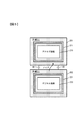
- FIG. 1 is a diagram showing a configuration example of a camera 1 which is an example of the image pickup apparatus according to the first embodiment.
- the camera 1 includes a photographing optical system (imaging optical system) 2, an image sensor 3, a control unit 4, a memory 5, a display unit 6, and an operation unit 7.
- the photographing optical system 2 has a plurality of lenses including a focus adjusting lens (focus lens) and an aperture diaphragm, and forms a subject image on the image pickup element 3.
- the photographing optical system 2 may be detachable from the camera 1.
- the image sensor 3 is an image sensor such as a CMOS image sensor or a CCD image sensor.
- the image sensor 3 receives the light flux that has passed through the photographing optical system 2 and images a subject image formed by the photographing optical system 2.
- a plurality of pixels having a photoelectric conversion unit are arranged in a two-dimensional shape (row direction and column direction) in the image sensor 3.
- the photoelectric conversion element is composed of a photodiode (PD).
- PD photodiode
- Memory 5 is a recording medium such as a memory card. Image data, a control program, and the like are recorded in the memory 5. The writing of data to the memory 5 and the reading of data from the memory 5 are controlled by the control unit 4.
- the display unit 6 displays an image based on the image data, information on shooting such as a shutter speed and an aperture value, a menu screen, and the like.
- the operation unit 7 includes various setting switches such as a release button, a power switch, and a switch for switching various modes, and outputs a signal based on each operation to the control unit 4.
- the control unit 4 is composed of a processor such as a CPU, FPGA, and ASIC, and a memory such as ROM and RAM, and controls each part of the camera 1 based on a control program.
- the control unit 4 supplies a signal for controlling the image sensor 3 to the image sensor 3 to control the operation of the image sensor 3. Further, the control unit 4 performs various image processing on the signal output from the image sensor 3 to generate image data.
- the control unit 4 is also an image generation unit that generates image data, and generates still image data and moving image data based on a signal output from the image sensor 3.
- the image processing includes known image processing such as gradation conversion processing and color interpolation processing.
- the control unit 4 performs a process of individually reading out the signals of each pixel of the image sensor 3 and a process of adding and reading out the signals of a plurality of pixels. For example, the control unit 4 performs a process of adding and reading signals of a plurality of pixels when displaying a through image (live view image) of a subject on the display unit 6 or when shooting a moving image. Further, the control unit 4 performs a process of individually reading out the signal of each pixel when shooting a high-resolution still image.
- FIG. 2 is a diagram showing a configuration example of the image sensor according to the first embodiment.
- the image sensor 3 includes a pixel unit (pixel area) 20, a column circuit unit 40 (column circuit unit 40a, column circuit unit 40b), a horizontal transfer unit 50 (horizontal transfer unit 50a, horizontal transfer unit 50b), and a processing unit. It has 60 (processing unit 60a, processing unit 60b) and a signal output unit 70 (signal output unit 70a, signal output unit 70b). Further, the image sensor 3 includes a read control unit 100, a first supply unit 110 (first supply unit 110a, first supply unit 110b), and a second supply unit 120 (second supply unit 120a, It has a second supply unit 120b).
- the number and arrangement of pixels arranged in the pixel unit 20 is not limited to the illustrated example.
- the pixel 10 is provided with any one of three color filters (color filters) 18 having different spectral characteristics of red (R), green (G), and blue (B).
- the pixel 10 was incident with a pixel (hereinafter, referred to as an R pixel) having a color filter 18 having a spectral characteristic for dispersing light in the first wavelength region (red (R) light) among the incident light.
- a pixel (hereinafter referred to as G pixel) having a color filter 18 having spectral characteristics for dispersing light in the second wavelength region of light (light of green (G)) and a third wavelength of the incident light.
- the image sensor 3 has a first pixel row in which R pixels 10 and G pixels 10 are alternately arranged in the left-right direction, that is, in the row direction (horizontal direction), and G pixels 10 and B pixels. It has a second pixel row in which 10 and 10 are alternately arranged in the row direction. The first pixel row and the second pixel row are arranged alternately in the column direction.
- the R pixel 10, the G pixel 10, and the B pixel 10 are arranged according to the Bayer arrangement.
- the image sensor 3 is provided with vertical signal lines 25 (vertical signal lines 25a, vertical signal lines 25b) for each pixel row, which is a row of a plurality of pixels 10 arranged in the vertical direction, that is, in the row direction (vertical direction). ..
- the plurality of vertical signal lines 25a are connected to the pixel rows of the odd-numbered rows, respectively.
- the plurality of vertical signal lines 25b are connected to the even-numbered pixel rows, respectively.
- the read control unit 100 is commonly provided for a plurality of pixel strings.
- the read-out control unit 100 is controlled by the control unit 4 of the camera 1 and supplies signals such as a signal TX, a signal RST, and a signal SEL, which will be described later, to each pixel 10 to control the operation of each pixel 10.
- the read control unit 100 supplies a signal to the gate of each transistor of the pixel 10, and turns the transistor on (connected state, conducting state, short-circuited state) or off state (disconnected state, non-conducting state, open state, cutoff state). ).
- the signal of the pixel of the pixel unit 20 selected by the read-out control unit 100 is output to the vertical signal line 25 connected to the pixel 10.
- a column circuit unit 40a is provided for an odd number of pixel rows among the plurality of pixels 10 of the pixel unit 20.
- the column circuit unit 40a includes a plurality of current sources 41a, a horizontal addition unit 42a, and a plurality of analog / digital conversion units (AD conversion units) 43a.
- the current source 41a and the AD conversion unit 43a in the column circuit unit 40a are provided for each vertical signal line 25a.
- the current source 41a is connected to each pixel 10 via the vertical signal line 25a.
- the current source 41a generates a current for reading a signal from the pixel 10, and supplies the generated current to the vertical signal line 25a and each pixel 10.
- the horizontal addition unit 42a is composed of a plurality of switches and adds the signals of the pixels output to the vertical signal line 25a.
- the read control unit 100 controls on / off of a plurality of switches constituting the horizontal addition unit 42a to control the addition processing of signals of a plurality of pixels arranged in the row direction (horizontal direction).
- the AD conversion unit 43a converts the signal input from each pixel 10 via the horizontal addition unit 42a into a digital signal, and outputs the converted digital signal to the horizontal transfer unit 50a.
- a column circuit unit 40b is provided for an even number of pixel rows among the plurality of pixels 10 of the pixel unit 20.
- the column circuit unit 40b includes a plurality of current sources 41b, a horizontal addition unit 42b, and a plurality of AD conversion units 43b.
- the current source 41b and the AD conversion unit 43b in the column circuit unit 40b are provided for each vertical signal line 25b.
- the current source 41b is connected to each pixel 10 via the vertical signal line 25b.
- the current source 41b generates a current for reading a signal from the pixel 10, and supplies the generated current to the vertical signal line 25b and each pixel 10.
- the horizontal addition unit 42b is composed of a plurality of switches and adds the signals of the pixels output to the vertical signal line 25b.
- the read control unit 100 controls on / off of a plurality of switches constituting the horizontal addition unit 42b to control a signal addition process between a plurality of pixels arranged in the row direction (horizontal direction).
- the AD conversion unit 43b converts the signal input from each pixel 10 via the horizontal addition unit 42b into a digital signal, and outputs the converted digital signal to the horizontal transfer unit 50b.
- the horizontal transfer unit 50a is provided for a plurality of AD conversion units 43a, and sequentially outputs the signal converted into a digital signal by each AD conversion unit 43a to the processing unit 60a.
- the horizontal transfer unit 50b is provided for a plurality of AD conversion units 43b, and sequentially outputs the signals converted into digital signals by each AD conversion unit 43b to the processing unit 60b. In this way, in the image sensor 3, the signals of the pixels in the odd-numbered columns and the signals of the pixels in the even-numbered columns are read out by different paths.
- the first supply unit 110a has a current source, generates a current for operating the AD conversion unit 43a, and supplies the generated current to the AD conversion unit 43a.
- the first supply unit 110b has a current source, generates a current for operating the AD conversion unit 43b, and supplies the generated current to the AD conversion unit 43b.
- the first supply unit 110a and the first supply unit 110b are each controlled by the read control unit 100.
- the processing unit 60a and the processing unit 60b are configured to include an amplifier circuit, a decoder circuit, and the like, respectively.
- a pixel signal converted into a digital signal from the horizontal transfer unit 50a is input to the processing unit 60a.
- the processing unit 60a performs signal processing such as code conversion processing and correlation double sampling on the signal input from the horizontal transfer unit 50a, and outputs the signal to the signal output unit 70a.
- a pixel signal converted into a digital signal from the horizontal transfer unit 50b is input to the processing unit 60b.
- the processing unit 60b performs signal processing such as code conversion processing and correlation double sampling on the signal input from the horizontal transfer unit 50b, and outputs the signal to the signal output unit 70b.
- the second supply unit 120a generates a control signal for operating the processing unit 60a, a pulse signal (pulse) in the present embodiment, and supplies the generated pulse signal to the processing unit 60a.
- the second supply unit 120b generates a control signal for operating the processing unit 60b, a pulse signal in the present embodiment, and supplies the generated pulse signal to the processing unit 60b.
- the second supply unit 120a and the second supply unit 120b are each controlled by the read control unit 100. Note that these control signals may be signals having a constant potential (for example, power supply potential).
- the signal output unit 70a and the signal output unit 70b each have an output circuit corresponding to a high-speed interface such as SLVS or LVDS.
- the signal output unit 70a outputs (transmits) the signal input from the processing unit 60a to the control unit 4 of the camera 1 at high speed.
- the signal output unit 70b outputs the signal input from the processing unit 60b to the control unit 4 at high speed.
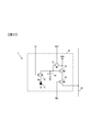
- FIG. 3 is a diagram showing a configuration example of pixels of the image sensor according to the first embodiment.
- the pixel 10 includes a photoelectric conversion unit 11, a transfer unit 12, a reset unit 13, a floating diffusion (FD) 14, an amplification unit 15, and a selection unit 16.
- the photoelectric conversion unit 11 is a photodiode PD, which converts incident light into electric charges and stores the photoelectrically converted electric charges.
- the transfer unit 12 is composed of a transistor M1 controlled by a signal TX, and transfers the charge photoelectrically converted by the photoelectric conversion unit 11 to the FD 14.
- the transistor M1 is a transfer transistor.
- the capacitance C of the FD 14 accumulates (holds) the electric charge transferred to the FD 14 and converts it into a voltage.
- the amplification unit 15 is composed of a transistor M3 whose gate (terminal) is connected to the FD 14, and outputs a signal based on the voltage of the capacitance C of the FD 14.
- the amplification unit 15 is connected to the vertical signal line 25 via the selection unit 16.
- the transistor M3 is an amplification transistor.
- the amplification unit 15 and the selection unit 16 form an output unit that generates and outputs a signal based on the electric charge generated by the photoelectric conversion unit 11.
- the reset unit 13 is composed of the transistor M2 controlled by the signal RST, discharges the electric charge accumulated in the FD 14, and resets the voltage of the FD 14.
- the transistor M2 is a reset transistor.
- the selection unit 16 is composed of a transistor M4 controlled by a signal SEL, and electrically connects or disconnects the amplification unit 15 and the vertical signal line 25.
- the transistor M4 of the selection unit 16 outputs a signal from the amplification unit 15 to the vertical signal line 25 when it is in the ON state.
- the transistor M4 is a selection transistor.
- the pixel 10 transmits a signal (dark signal) when the voltage of the FD 14 is reset and a signal (photoelectric conversion signal) corresponding to the electric charge transferred from the photoelectric conversion unit 11 to the FD 14 by the transfer unit 12 as a vertical signal line 25. Output sequentially to.
- the dark signal is an analog signal indicating a reference level for the photoelectric conversion signal.
- the photoelectric conversion signal is an analog signal generated based on the charge photoelectrically converted by the photoelectric conversion unit 11.
- the dark signal and the photoelectric conversion signal sequentially output from the pixel 10 are input to the horizontal addition unit 42 via the vertical signal line 25.
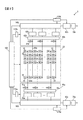
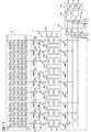
- FIG. 4 is a diagram showing a partial configuration example of the image pickup device according to the first embodiment.
- FIG. 4 shows a part of pixels 10 among a plurality of pixels provided in the image sensor 3, a column circuit unit 40a, a horizontal transfer unit 50a, a processing unit 60a, and a signal output unit 70a. .. Further, in FIG. 4, the pixel 10 in the upper left corner is the pixel 10 (1,1) in the first row and the first column, and the pixel 10 in the lower right corner is the pixel 10 (5, 17) in the fifth row and the 17th column. , 85 pixels 10 of 17 pixels in the row direction ⁇ 5 pixels in the column direction are illustrated.
- the horizontal addition unit 42a is a switch that connects or disconnects the vertical signal line 25a (vertical signal line 25a1 to vertical signal line 25a9 in FIG. 4) and the AD conversion unit 43a (AD conversion unit 43a1 to AD conversion unit 43a9 in FIG. 4). It has SW1 (SW1a to SW1i in FIG. 4). Further, the horizontal addition unit 42a has switches SW2 (SW2a to SW2f in FIG. 4) for connecting or disconnecting adjacent vertical signal lines 25a.
- the switch SW2 is a connection portion that connects the vertical signal lines 25.
- the switch SW1 and the switch SW2 are on / off controlled by the read control unit 100 (see FIG. 2).
- the AD conversion unit 43a is configured to include a comparison unit 44 and a storage unit 45, and converts a pixel signal input via the horizontal addition unit 42a into a digital signal having a predetermined number of bits.
- the comparison unit 44 includes a comparator circuit. A current for operating the comparator circuit is supplied to the comparison unit 44 of the AD conversion unit 43a from the first supply unit 110a (see FIG. 2).
- the comparison unit 44 compares the signal output from the pixel 10 with the reference signal (lamp signal) that changes constantly with the passage of time, and outputs the output signal as the comparison result to the storage unit 45.
- the storage unit 45 is composed of a plurality of latch circuits corresponding to the number of bits of the digital signal to be stored. An output signal indicating a comparison result is input to the storage unit 45 from the comparison unit 44, and a clock signal indicating a count value is input from a counter circuit (not shown).
- the storage unit 45 stores as a digital signal a count value according to the elapsed time from the start of comparison by the comparison unit 44 until the comparison result is inverted, based on the output signal of the comparison unit 44 and the clock signal from the counter circuit. .. In other words, the storage unit 45 responds to the time until the magnitude relationship between the level of the signal output from the pixel 10 and the level of the reference signal changes (inverts) based on the signal output from the comparison unit 44.
- the count value is stored as a digital signal.
- the comparison unit 44 compares the dark signal with the reference signal and outputs the comparison result to the storage unit 45. Based on the comparison result by the comparison unit 44 and the clock signal, the storage unit 45 sets a count value according to the elapsed time from the start of the comparison by the comparison unit 44 to the inversion of the comparison result as a digital signal corresponding to the dark signal.
- the comparison unit 44 compares the photoelectric conversion signal with the reference signal and outputs the comparison result to the storage unit 45. To do.
- the storage unit 45 Based on the comparison result by the comparison unit 44 and the clock signal, the storage unit 45 sets a count value according to the elapsed time from the start of the comparison by the comparison unit 44 to the inversion of the comparison result as a digital signal according to the photoelectric conversion signal.
- the AD conversion unit 43a converts the photoelectric conversion signal, which is an analog signal, into a digital signal having a predetermined number of bits, and converts the dark signal, which is an analog signal, into a digital signal having a predetermined number of bits. Further, the AD conversion unit 43a has an output circuit (not shown) that operates by the current supplied from the first supply unit 110a, and outputs the digital signal stored in the storage unit 45 to the horizontal transfer unit 50a.
- the horizontal transfer unit 50a has a switch SW3 (SW3a to SW3i in FIG. 4), a data lane 55 (data lanes 55a to 55c), a sense amplifier 62 (sense amplifiers 62a to 62c), and an AND circuit 61.
- the switch SW3 is on / off controlled by the read control unit 100 (see FIG. 2) to connect or disconnect the AD conversion unit 43a and the data lane 55.
- the data lane 55 is provided for a plurality of AD conversion units 43a, and transfers (transmits) a digital signal input from each AD conversion unit 43a via the switch SW3 to the sense amplifier 62.
- the data lane 55 is a transmission line for transmitting a pixel signal converted into a digital signal.
- the horizontal transfer unit 50a has a data lane 55a, a data lane 55b, and a data lane 55c.
- Each of the data lanes 55a to 55c is composed of a plurality of signal lines corresponding to the number of bits of the transmitted digital signal.
- the sense amplifier 62 is composed of a plurality of amplifier circuits corresponding to the number of bits of the input digital signal, and is arranged for each data lane 55.
- the sense amplifier 62a is provided for the data lane 55a
- the sense amplifier 62b is provided for the data lane 55b
- the sense amplifier 62c is provided for the data lane 55c.
- a control signal for operating the amplifier circuit and a pulse signal in the present embodiment are supplied to the sense amplifiers 62a to 62c from the second supply unit 120a (see FIG. 2), respectively.
- the sense amplifiers 62a to 62c amplify and read the signal input to the data lane 55 connected to each of them.
- the control signal for operating the amplifier circuit may be a signal having a constant potential (for example, a power supply potential).
- a signal V1 and a signal V2 are input to the AND circuit 61.
- the signal V1 is also input to the sense amplifier 62b.
- the output signal of the AND circuit 61 is input to the sense amplifier 62a and the sense amplifier 62c, respectively.
- the signal V1 and the signal V2 are signals used for controlling the sense amplifiers 62a to 62c.
- the read control unit 100 controls the operating states of the sense amplifiers 62a to 62c by controlling the signal V1 and the signal V2. In this way, the horizontal transfer unit 50a sequentially outputs the signal converted into the digital signal by each AD conversion unit 43a to the processing unit 60a.
- the processing unit 60a has a signal processing unit 64 (signal processing units 64a to 64c).
- the signal processing unit 64 is provided for each sense amplifier 62.
- the signal processing unit 64a is provided for the sense amplifier 62a
- the signal processing unit 64b is provided for the sense amplifier 62b
- the signal processing unit 64c is provided for the sense amplifier 62c.
- the signal processing unit 64 is composed of a decoding circuit, a memory circuit, and the like.
- the signal processing unit 64 performs signal processing such as code conversion processing and correlation double sampling on the signal input from the sense amplifier 62.
- the signal processing unit 64 outputs the signal after signal processing to the signal output unit 70a.
- the signal output unit 70a has output I / F units 71a to 71c.
- the output I / F units 71a to 71c are configured by an output circuit corresponding to a high-speed interface such as SLVS.
- the output I / F unit 71a outputs the signal input from the signal processing unit 64a to the control unit 4 of the camera 1.
- the output I / F unit 71b outputs the signal input from the signal processing unit 64b to the control unit 4, and the output I / F unit 71c outputs the signal input from the signal processing unit 64c to the control unit 4. To do.
- the configurations of the column circuit unit 40b, the horizontal transfer unit 50b, the processing unit 60b, and the signal output unit 70b are also the same as the configurations of the column circuit unit 40a, the horizontal transfer unit 50a, the processing unit 60a, and the signal output unit 70a described above. The same is true.
- the read control unit 100 controls each switch of the horizontal addition unit 42 and the horizontal transfer unit 50 to individually read out the signal of each pixel of the image sensor 3 (individual read control), and a plurality of times. A process of adding and reading pixel signals (additional reading control) is performed.
- the control unit 4 of the camera 1 controls the read control unit 100 to switch the pixel signal reading method.
- the read control unit 100 turns off the switch SW2 of the horizontal addition unit 42, sequentially selects a plurality of pixels of the image sensor 3 line by line, and outputs the signal of the selected pixel to the AD conversion unit 43. To output to. Further, the read control unit 100 uses the plurality of data lanes 55 of the horizontal transfer unit 50 to sequentially output the pixel signals converted into digital signals by each AD conversion unit 43 to the processing unit 60.
- the reading control unit 100 turns on the switch SW2 of the horizontal addition unit 42, sequentially selects a plurality of pixels of the image pickup element 3 line by line, and transmits signals of the plurality of pixels on the vertical signal line 25. to add.
- the read-out control unit 100 outputs the signal of the added pixels to the AD conversion unit 43, which is a part of the plurality of AD conversion units 43 arranged in the image sensor 3.
- a part of the AD conversion unit 43 to which the signal of the added pixels is input is connected to a part of the data lanes 55 of the plurality of data lanes 55 of the horizontal transfer unit 50. Will be done. Therefore, in the addition / reading control, the reading control unit 100 processes the signal of the pixel converted into a digital signal by each AD conversion unit 43 by using only a part of the data lanes 55 among the plurality of data lanes 55. It is possible to make the unit 60 output sequentially.
- the read control unit 100 uses a part of the AD conversion unit 43 and a part of the data lane 55 when performing the addition / read control.
- the other AD conversion unit 43 to which the signal of the added pixel is not input, the data lane 55 to which the AD conversion unit 43 is connected, and the sense amplifier 62 connected to the data lane 55 are added / read controlled.
- the read control unit 100 controls the first supply unit 110 to stop the current supplied to the AD conversion unit 43, which is not used when performing the addition / read control. Further, the read control unit 100 stops the operation of the data lane 55 which is not used when performing the addition read control.
- the read control unit 100 controls the second supply unit 120 to stop the operation of the sense amplifier 62 which is not used when performing the addition read control. As a result, the power consumption of the image sensor 3 can be reduced. Therefore, when shooting a moving image at a high frame rate, it is possible to suppress an increase in power consumption by performing addition / reading control.
- the AD conversion unit 43 used when performing addition / reading control is, for example, an AD conversion unit 43a2, an AD conversion unit 43a5, and an AD conversion unit 43a8.
- the AD conversion unit 43a2, the AD conversion unit 43a5, and the AD conversion unit 43a8 are connected to the same data lane 55b among the plurality of data lanes 55a to 55c via the switch SW3b, the switch SW3e, and the switch SW3h, respectively.
- a part of the AD conversion unit 43 (AD conversion units 43a2, 43a5, 43a8 in FIG. 4), a part of the data lane 55 (data lane 55b in FIG. 4), and a part of the sense amplifier 62 (in FIG. 4) of the image sensor 3.
- the sense amplifier 62b) constitutes a first output unit that outputs the pixel signal output to the vertical signal line 25 to the processing unit 60.
- the first output unit is supplied with the current from the first supply unit 110 and the pulse signal from the second supply unit 120 both when the individual read control is performed and when the additive read control is performed. It becomes an operating state.
- AD conversion units 43 AD conversion units 43a1, 43a3, 43a4, 43a6, 43a7, 43a9 in FIG. 4
- other data lanes 55 data lanes 55a, 55c in FIG. 4
- the 62 sense amplifiers 62a and 62c in FIG. 4 constitutes a second output unit that outputs the pixel signal output to the vertical signal line 25 to the processing unit 60.
- the second output unit is put into an operating state by being supplied with a current from the first supply unit 110 and a pulse signal from the second supply unit 120.
- the addition / reading control is performed, the pixel signal is not input to the second output unit.
- the read control unit 100 stops the supply of current to the second output unit by the first supply unit 110, and causes the second supply unit 120 to pulse to the second output unit. Stop the signal supply.
- the second output unit is stopped without the current being supplied from the first supply unit 110 and the pulse signal not being supplied from the second supply unit 120.
- the sense amplifier 62 (sense amplifiers 62a and 62c in FIG. 4) of the second output unit is not used in the addition / reading control.
- the read control unit 100 causes the second supply unit 120 to stop the supply of the pulse signal to the sense amplifiers 62a and 62c.
- the sense amplifiers 62a and 62c are stopped (paused) without being supplied with the pulse signal from the second supply unit 120.
- the second output unit is stopped, and the power consumption of the image sensor 3 is reduced.
- the read control unit 100 When the individual read control is selected (set) by the control unit 4, the read control unit 100 turns on the switches SW1a to SW1i of the horizontal addition unit 42 and turns off the switches SW2a to SW2f. Further, the read control unit 100 sets both the signal V1 and the signal V2 to a high level. As a result, the sense amplifiers 62a to 62c are in a state where they can amplify and read the input signal.
- the read control unit 100 turns on the reset units 13 of the R pixels 10 (1,1) to the R pixels 10 (1,17), which are the pixels of the first row. As a result, the voltage of each FD 14 is reset in the pixel 10 in the first row. Further, the selection unit 16 of the pixel 10 in the first row is turned on. The read control unit 100 turns off the selection units 16 of the pixels 10 in the rows other than the first row. As a result, each dark signal of the R pixel 10 (1,1) to the R pixel 10 (1,17) in the first row is the selection unit 16 of each pixel and the vertical signal line connected to each pixel. It is output to the AD conversion unit 43a1 to the AD conversion unit 43a9 via the vertical signal lines 25a9 from 25a1 and the switches SW1a to SW1i, respectively.
- the AD conversion unit 43a1 to the AD conversion unit 43a9 convert the input dark signal into a digital signal.
- the read control unit 100 controls the switches SW3a to SW3i of the horizontal transfer unit 50a to sequentially output the dark signal converted into a digital signal by each AD conversion unit 43a to the processing unit 60a via the sense amplifier 62. ..
- the read control unit 100 outputs the digital signals converted by the AD conversion units 43a1 to 43a3 to the processing units 60a via the data lanes 55a to 55c, respectively, with only the switches SW3a to SW3c of the switches SW3a to SW3i turned on. Let me.
- the read control unit 100 turns on only the switches SW3d to SW3f among the switches SW3a to SW3i, and processes the digital signals converted by the AD conversion units 43a4 to 43a6 via the data lanes 55a to 55c, respectively. To output to. After that, the read control unit 100 turns on only the switches SW3g to SW3i among the switches SW3a to SW3i, and processes the digital signals converted by the AD conversion units 43a7 to 43a9 via the data lanes 55a to 55c, respectively. To output to.
- the read control unit 100 turns on the transfer units 12 of the R pixels 10 (1,1) to the R pixels 10 (1,17), which are the pixels of the first row. As a result, in the pixel 10 of the first row, the charge photoelectrically converted in each PD 11 is transferred to the FD 14.
- the photoelectric conversion signals of the R pixels 10 (1,1) to the R pixels 10 (1,17) in the first row are the selection unit 16 of each pixel, the vertical signal line 25 connected to each pixel, and the like. It is output to the AD conversion unit 43a1 to the AD conversion unit 43a9, respectively, via the switch SW1.
- the AD conversion unit 43a1 to the AD conversion unit 43a9 convert the input photoelectric conversion signal into a digital signal.
- the photoelectric conversion signals converted into digital signals by the AD conversion units 43a1 to 43a9 are processed via the data lanes 55a to 55c, respectively, in the same manner as when the dark signals converted into digital signals are sequentially output to the processing units 60a. It is sequentially output to unit 60a.
- the read control unit 100 reads a dark signal and photoelectric signals from pixels 10 (2, 1) to 10 (2, 17), which are pixels in the second row, in the same manner as in the case of reading a signal from the pixels in the first row. Read the converted signal. Similarly, the read control unit 100 sequentially selects the pixels of the third and subsequent rows one by one in the order of the third row, the fourth row, the fifth row, and the sixth row, and signals from each selected pixel. Is read.
- the read control unit 100 individually reads the signal of the pixel of the image sensor 3.
- the dark signal and photoelectric conversion signal sequentially output to the data lanes 55a to 55c are subjected to signal processing such as correlation double sampling by the processing unit 60a.
- the signal output to the data lane 55a is input to the signal processing unit 64a via the sense amplifier 62a, processed by the signal processing unit 64a, and then output to the control unit 4 by the output I / F unit 71a.
- the signal output to the data lane 55b is input to the signal processing unit 64b via the sense amplifier 62b, processed by the signal processing unit 64b, and then output to the control unit 4 by the output I / F unit 71b.
- the signal output to the data lane 55c is input to the signal processing unit 64c via the sense amplifier 62c, and after the signal processing is performed by the signal processing unit 64c, the output I / F unit 71c sends the signal to the control unit 4. It is output.
- addition / reading control a case where signals of the same color pixels are added and read out for each of three pixels in the row direction will be described.
- the read control unit 100 When the addition / reading control is selected by the control unit 4, the read control unit 100 turns on the switch SW1b, the switch SW1e, and the switch SW1h of the horizontal addition unit 42. The read control unit 100 turns off the switch SW1a, the switch SW1c, the switch SW1d, the switch SW1f, the switch SW1g, and the switch SW1i. Further, the read control unit 100 turns on the switch SW2a to the switch SW2f. The read control unit 100 controls the first supply unit 110a to stop the supply of current to the AD conversion units 43a1, 43a3, 43a4, 43a6, 43a7, 43a9. Further, the read control unit 100 sets the signal V1 to a high level so that the sense amplifier 62b can operate, and sets the signal V2 to a low level to stop the sense amplifier 62a and the sense amplifier 62c.
- the read control unit 100 turns on the reset units 13 of the R pixels 10 (1,1) to the R pixels 10 (1,17), which are the pixels of the first row. In addition, the selection units 16 of the pixels in the first row are turned on. The read control unit 100 turns off the pixel selection units 16 of the pixels in the rows other than the first row. Since both the switch SW2a and the switch SW2b are in the ON state, each amplification unit 15 of the R pixel 10 (1,1), the R pixel 10 (1,3), and the R pixel 10 (1,5) is a vertical signal. It is electrically connected via the wires 25a1 to 25a3.
- the dark signal of the R pixel 10 (1,1), the dark signal of the R pixel 10 (1,3), and the dark signal of the R pixel 10 (1,5) are added and averaged. Further, since the switch SW1b is in the ON state, the added dark signal is output to the AD conversion unit 43a2.
- the dark signal of the R pixel 10 (1,7), the dark signal of the R pixel 10 (1,9), and the dark signal of the R pixel 10 (1,11) are added and averaged, and the dark signal of the R pixel 10 (1,11) is added and averaged, and the dark signal is added and averaged, and the dark signal is passed through the switch SW1e. It is output to the AD conversion unit 43a5. Further, the dark signal of the R pixel 10 (1,13), the dark signal of the R pixel 10 (1,15), and the dark signal of the R pixel 10 (1,17) are added and averaged, and AD is performed via the switch SW1h. It is output to the conversion unit 43a8.
- the AD conversion unit 43a2, the AD conversion unit 43a5, and the AD conversion unit 43a8 each convert the added dark signal into a digital signal.
- the read control unit 100 sequentially turns on the switch SW3b, the switch SW3e, and the switch SW3h of the horizontal transfer unit 50a, and sends the digital signal converted by each AD conversion unit 43a to the processing unit 60a via the sense amplifier 62. Output sequentially.
- the read control unit 100 turns on only the switch SW3b among the switches SW3a to SW3i, and outputs the digital signal converted by the AD conversion unit 43a2 to the processing unit 60a via the data lane 55b.
- the read control unit 100 turns on only the switch SW3e of the switches SW3a to SW3i, and outputs the digital signal converted by the AD conversion unit 43a5 to the processing unit 60a via the data lane 55b.
- the read control unit 100 turns on only the switch SW3h among the switches SW3a to SW3i, and outputs the digital signal converted by the AD conversion unit 43a8 to the processing unit 60a via the data lane 55b.
- the read control unit 100 turns on the transfer units 12 of the R pixels 10 (1,1) to the R pixels 10 (1,17), which are the pixels of the first row. As a result, in the pixel 10 of the first row, the charge photoelectrically converted in each PD 11 is transferred to the FD 14. Since both the switch SW2a and the switch SW2b are in the ON state, each amplification unit 15 of the R pixel 10 (1,1), the R pixel 10 (1,3), and the R pixel 10 (1,5) is a vertical signal. It is electrically connected via the wires 25a1 to 25a3.
- the photoelectric conversion signal of the R pixel 10 (1,1), the photoelectric conversion signal of the R pixel 10 (1,3), and the photoelectric conversion signal of the R pixel 10 (1,5) are added and averaged. Further, since the switch SW1b is in the ON state, the added and averaged photoelectric conversion signal is output to the AD conversion unit 43a2.
- the photoelectric conversion signal of the R pixel 10 (1,7), the photoelectric conversion signal of the R pixel 10 (1,9), and the photoelectric conversion signal of the R pixel 10 (1,11) are added and averaged, and the switch SW1e Is output to the AD conversion unit 43a5 via. Further, the photoelectric conversion signal of the R pixel 10 (1,13), the photoelectric conversion signal of the R pixel 10 (1,15), and the photoelectric conversion signal of the R pixel 10 (1,17) are added and averaged, and the switch SW1h is pressed. It is output to the AD conversion unit 43a8 via the device.
- the AD conversion unit 43a2, the AD conversion unit 43a5, and the AD conversion unit 43a8 each convert the added photoelectric conversion signal into a digital signal.
- the read control unit 100 sequentially turns on the switch SW3b, the switch SW3e, and the switch SW3h of the horizontal transfer unit 50a, and sends the digital signal converted by each AD conversion unit 43a to the processing unit 60a via the sense amplifier 62. Output sequentially.
- the read control unit 100 turns on only the switch SW3b among the switches SW3a to SW3i, and outputs the digital signal converted by the AD conversion unit 43a2 to the processing unit 60a via the data lane 55b.
- the read control unit 100 turns on only the switch SW3e of the switches SW3a to SW3i, and outputs the digital signal converted by the AD conversion unit 43a5 to the processing unit 60a via the data lane 55b.
- the read control unit 100 turns on only the switch SW3h among the switches SW3a to SW3i, and outputs the digital signal converted by the AD conversion unit 43a8 to the processing unit 60a via the data lane 55b.
- the read control unit 100 adds from the pixels 10 (2, 1) to 10 (2, 17), which are the pixels of the second row, in the same manner as in the case of reading the signal added from the pixels of the first row.
- the dark signal and the photoelectric conversion signal are read out.
- the read control unit 100 sequentially selects the pixels of the third and subsequent rows one by one in the order of the third row, the fourth row, the fifth row, and the sixth row, and signals from each selected pixel. Is read.
- the reading control unit 100 adds and reads the signals of the plurality of pixels of the image pickup device 3.
- the added dark signal and photoelectric conversion signal are converted into digital signals by the AD conversion unit 43, and then sequentially output to the data lane 55b.
- the dark signal and photoelectric conversion signal sequentially output to the data lane 55b are input to the signal processing unit 64b via the sense amplifier 62b, and are output after signal processing such as correlation double sampling is performed by the signal processing unit 64b. It is output to the control unit 4 by the I / F unit 71b.
- FIG. 5 is a diagram showing a layout example of a part of the image sensor according to the first embodiment.
- the image pickup device 3 is configured by using a semiconductor substrate having p-well 201 and p-well 202.
- the p-well 201 is provided with a region 210 and a region 211 formed so as to surround the region 210.
- the p-well 202 is provided with a region 220 and a region 221 formed so as to surround the region 220.
- the region 210 in the p-well 201 is a region (analog circuit region) in which the elements constituting the analog circuit are formed.
- the comparison unit 44 of the AD conversion unit 43 is provided in the analog circuit area 210.
- the region 220 in the p-well 202 is a region (digital circuit region) in which the elements constituting the digital circuit are formed.
- the storage unit 45 and the horizontal transfer unit 50 are provided in the digital circuit area 220.
- the region 211 and the region 221 are p + regions formed by using p-type impurities, respectively. Regions 211 and 221 respectively function as guard rings to prevent charge from leaking into adjacent regions.
- the analog circuit area 210 and the digital circuit area 220 are arranged close to each other, and a parasitic capacitance 90 is formed between the analog circuit area 210 and the digital circuit area 220. Further, since the comparison unit 44 of the analog circuit area 210 and the horizontal transfer unit 50 of the digital circuit area 220 are arranged relatively close to each other, they may interfere with each other via the parasitic capacitance 90 to generate noise. If the operating state of the horizontal transfer unit 50 changes while the AD conversion unit 43 is performing the AD conversion, the noise interference state changes during the AD conversion, so that the AD conversion result may vary. The accuracy of AD conversion may decrease due to the change in the magnitude of noise exerted by the horizontal transfer unit 50 on the AD conversion unit 43.
- the AD conversion unit 43 used in the addition / reading control is connected to different data lanes 55.
- the AD conversion unit 43a2 is connected to the data lane 55a
- the AD conversion unit 43a5 is connected to the data lane 55b
- the AD conversion unit 43a8 is connected to the data lane 55c.
- the reading control unit 100 when performing addition / reading control, the reading control unit 100 outputs the digital signal converted by the AD conversion unit 43a2 to the data lane 55a, and outputs the digital signal converted by the AD conversion unit 43a5 to the data lane.
- the operation of outputting to the 55b and the operation of outputting the digital signal converted by the AD conversion unit 43a8 to the data lane 55c are performed at the same time.
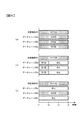
- FIG. 6 is a diagram comparing the read control according to the first embodiment and the read control according to the comparative example.
- FIG. 6A shows the operating states of the AD conversion unit 43 and the data lanes 55a to 55c when the image sensor according to the present embodiment performs individual read-out control.
- FIG. 6B shows the operating states of the AD conversion unit 43 and the data lanes 55a to 55c when the image sensor according to the comparative example performs additive / readout control.
- FIG. 6C shows the operating states of the AD conversion unit 43 and the data lanes 55a to 55c when the image sensor according to the present embodiment performs additive / readout control. Note that FIGS.
- FIGS. 6A to 6C in order to compare the operating states of the data lanes 55a to 55c during the period of the AD conversion process by the AD conversion unit 43, the signal of the pixel in the (N + 1) th row The AD conversion process and the signal transfer process of the pixel in the Nth row are shown side by side.
- the read control unit 100 sequentially outputs the signal of the pixel converted into the digital signal to the processing unit 60 by using the three data lanes 55a to 55c of the horizontal transfer unit 50. ..
- the data lanes 55a to 55c sequentially output the signal of the pixel in the Nth line to the processing unit 60.
- the period from time t1 to time t4 is a period (read period) for reading the signal of the pixel in the Nth row to the processing unit 60.
- the AD conversion units 43a1 to 43a9 sequentially convert the photoelectric conversion signal and the dark signal output from the pixels of the (N + 1) th row into digital signals.
- the period from time t1 to time t4 is a period for converting the signal of the pixel in the (N + 1) th row into a digital signal.
- the individual read control in the case of the comparative example is also the same as in FIG. 6A.
- the reading control unit 100 sequentially outputs the pixel signals to the processing unit 60 using the three data lanes 55a to 55c. Since the signals of the pixels are added and read by 3 pixels in the horizontal direction, the number of signals (data amount) transferred to the processing unit 60 by the horizontal transfer unit 50 is 1/3 of that in the case of individual read control. Become. Further, since the signal of the pixel with the number of signals of 1/3 is read out to the processing unit 60 using the three data lanes 55a to 55c as in the case of the individual read-out control, the read in the case of the additive read-out control according to the comparative example. The period is approximately 1/3 of the read period in the case of individual read control.
- the data lanes 55a to 55c are the Nth line input from the AD conversion units 43a2, 43a5, 43a8.
- the signals of the eye pixels are sequentially output to the processing unit 60.
- the reading of the signal of the Nth row pixel to the processing unit 60 is completed.
- the data lanes 55a to 55c are in a state in which the pixel signal is not input from the AD conversion unit 43 and is not used for data transfer.
- the AD conversion units 43a2, 43a5, 43a8 sequentially convert the photoelectric conversion signal and the dark signal of the added pixels in the (N + 1) th row into digital signals.
- the period from time t1 to time t4 is a period for converting the signal of the pixel in the (N + 1) th row into a digital signal, as in the case of individual read control.
- the data lanes 55a to 55c change from the operating state to the stopped state in the middle of the period in which the AD conversion process of the pixel signal of the (N + 1) th row is performed. Therefore, in the comparative example, when the addition / reading control is performed, the noise received by the AD conversion unit 43 changes during the period in which the AD conversion process is performed by the AD conversion unit 43. As a result, in the comparative example, the accuracy of the AD conversion is lowered. It is conceivable to transfer signals to the data lanes 55a to 55c during the period from time t2 to time t4 to suppress the change in noise received by the AD conversion unit 43, but in this case, the power consumption increases. Resulting in.
- the read control unit 100 uses one data lane 55b to sequentially output pixel signals to the processing unit 60 when performing additive read control.
- the data lane 55 used for the addition / reading control is aggregated into one data lane 55b.
- the data lane 55b outputs the pixel signals sequentially input from the AD conversion units 43a2, 43a5, and 43a8 to the processing unit 60 during the period from time t1 to time t4.
- the data lanes 55b are in the operating state
- the data lanes 55a and 55c are in the stopped state.
- the period from the time t1 to the time t4 is the period for reading the signal of the pixel in the Nth line to the processing unit 60, as in the case of performing the individual read control. ..
- the data lanes 55b remain in the operating state and the data lanes 55a and 55c are in the stopped state during the period in which the AD conversion process of the pixel signal in the (N + 1) th row is performed. There is up to. As a result, it is possible to prevent the noise received by the AD conversion unit 43 from changing during the period during which the AD conversion process is performed by the AD conversion unit 43. As a result, in the present embodiment, it is possible to prevent the accuracy of AD conversion from being lowered. Further, in the present embodiment, since the data lane 55 used for the addition / reading control is narrowed down, the power consumption can be reduced.
- the image pickup element 3 has a photoelectric conversion unit 11 that generates a charge by photoelectric conversion, and has a first pixel and a second pixel (pixel 10) that output a signal based on the charge generated by the photoelectric conversion unit 11.
- the first signal line for example, vertical signal line 25a2 that outputs the signal of the first pixel
- the second signal line for example, vertical signal line 25a3 that outputs the signal of the second pixel
- the first signal line are output.
- the first output unit (for example, AD conversion unit 43a2, data lane 55b, and sense amplifier 62b) that outputs at least one of the signal and the signal output to the second signal line to the processing unit 60 that processes the signal
- the second The second output unit (for example, AD conversion unit 43a3, data lane 55c, and sense amplifier 62c) that outputs the signal output to the signal line to the processing unit 60, and the signal of the first pixel and the signal of the second pixel
- a control unit (reading control unit 100) for performing the second control to be performed is provided.
- the image sensor 3 operates the first output unit of the first and second output units, and performs addition / reading control to output the signal of the added pixels to the processing unit 60. Therefore, the power consumption of the image sensor 3 can be reduced by stopping the second output unit when performing addition / reading control.
- the image sensor 3 uses the data lane 55b of the data lanes 55a to 55c when performing addition / reading control for adding and reading the pixel signals for each of three pixels in the horizontal direction.
- the signal of the added pixel is sequentially output to the processing unit 60.
- the data lanes 55b remain in the operating state
- the data lanes 55a and 55c remain in the stopped state. Therefore, it is possible to prevent the operating state of the data lane 55 from changing during the period in which the AD conversion process is performed by the AD conversion unit 43, and the noise received by the AD conversion unit 43 from changing. As a result, it is possible to suppress a decrease in the accuracy of AD conversion.
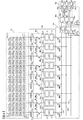
- FIG. 7 is a diagram showing a partial configuration example of the image pickup device according to the first modification.
- the image pickup device 3 according to the first modification includes an AND circuit 63.
- the clock signal CLK and the signal V3 are input to the AND circuit 63.
- the clock signal CLK is also input to the signal processing unit 64b.
- the output signal of the AND circuit 63 is input to the signal processing unit 64a and the signal processing unit 64c, respectively.
- the read control unit 100 controls the operating states of the signal processing units 64a and 64c by controlling the signal V3.
- the read control unit 100 sets the signal V3 to a high level when the individual read control is selected by the control unit 4.
- the clock signal CLK is input to the signal processing units 64a and 64c via the AND circuit 63.
- the signal processing units 64a to 64c can perform signal processing on the signal output from the sense amplifier 62 based on the clock signal CLK. It becomes a state.
- the read control unit 100 sets the signal V3 to a low level when the additive read control is selected by the control unit 4. As a result, the signal processing units 64a and 64c are stopped without inputting the clock signal. Since the clock signal CLK is input to the signal processing unit 64b, the signal processing unit 64b is in an operable state.
- the read control unit 100 controls the signal V3 input to the AND circuit 63 to control the operating states of the signal processing units 64a and 64c. Therefore, the read control unit 100 can reduce the power consumption of the image sensor 3 by stopping the signal processing units 64a and 64c when performing the addition / read control.
- FIG. 8 is a diagram showing a partial configuration example of the image pickup device according to the second modification.
- the image sensor 3 according to the second modification includes a conversion unit 65 and multiplexers 66a to 66c.
- the conversion unit 65 is connected to the signal processing unit 64b, and outputs the signal input from the signal processing unit 64b by dividing it into the multiplexers 66a to 66c.
- the multiplexer 66a is controlled by the read control unit 100, and selects a signal to be output to the output I / F unit 71a from a signal output by the signal processing unit 64a and a signal output by the conversion unit 65.
- the multiplexer 66b is controlled by the read control unit 100, and selects the signal output to the output I / F unit 71b from the signal output by the signal processing unit 64b and the signal output by the conversion unit 65.
- the multiplexer 66c is controlled by the read control unit 100, and selects the signal output to the output I / F unit 71c from the signal output by the signal processing unit 64c and the signal output by the conversion unit 65.
- the multiplexer 66a outputs the pixel signal input from the signal processing unit 64a to the output I / F unit 71a.
- the multiplexer 66b outputs the pixel signal input from the signal processing unit 64b to the output I / F unit 71b.
- the multiplexer 66c outputs a pixel signal input from the signal processing unit 64c to the output I / F unit 71c.
- the output I / F units 71a, 71b, and 71c output the signals input from the signal processing units 64a, 64b, and 64c to the control unit 4, respectively.
- the signal processing unit 64b performs signal processing on the pixel signals sequentially input via the data lane 55b and the sense amplifier 62b, and sequentially outputs the signals to the conversion unit 65.
- the conversion unit 65 divides the signals sequentially input from the signal processing unit 64b into the multiplexers 66a to 66c and outputs them.
- the multiplexer 66a outputs the pixel signal input from the conversion unit 65 to the output I / F unit 71a
- the multiplexer 66b outputs the pixel signal input from the conversion unit 65 to the output I / F unit 71b.
- the multiplexer 66c outputs a pixel signal input from the conversion unit 65 to the output I / F unit 71c.
- the output I / F units 71a, 71b, and 71c each output the signal input from the conversion unit 65 to the control unit 4.
- the pixel signal is output to the control unit 4 by one output I / F unit 71b out of the three output I / F units 71a to 71c.
- the pixel signals are output to the control unit 4 by the output I / F units 71a to 71c.
- Signals can be output to the control unit 4 from the three output I / F units 71a to 71c in both the case of performing the individual read control and the case of performing the additive read control.
- the number of output I / F units 71 used in the case of individual read control and the number of output I / F units 71 used in the case of additive read control can be made uniform. Therefore, it is possible to communicate the pixel signal between the image sensor 3 and the control unit 4 in the same manner as in the case of performing the addition / reading control and the case of performing the individual reading control.
- FIG. 9 is a diagram showing a partial configuration example of the image pickup device according to the modified example 3.
- the horizontal transfer unit 50 (horizontal transfer unit 50a in FIG. 9) has four data lanes 55: a data lane 55a, a data lane 55b, a data lane 55c, and a data lane 55d.
- the horizontal transfer unit 50 further includes a sense amplifier 62d.
- the processing unit 60 (processing unit 60a in FIG. 9) further includes a signal processing unit 64d and a multiplexer 66d.
- the signal output unit 70 (signal output unit 70a in FIG. 9) further has an output I / F unit 71d.
- the AD conversion unit 43 (AD conversion units 43a2, 43a5, 43a8 in FIG. 9) used in the addition / reading control is assigned to one of the two data lanes 55 (data lanes 55a, 55b in FIG. 9). Be connected.
- the AD conversion unit 43a2 is connected to the data lane 55b
- the AD conversion unit 43a5 is connected to the data lane 55a
- the AD conversion unit 43a8 is connected to the data lane 55b.
- the signal of the pixel of each line is AD via the selection unit 16 of each pixel, the vertical signal lines 25a1 to 25a9 connected to each pixel, and the switches SW1a to SW1i, respectively. It is output to the conversion unit 43a1 to the AD conversion unit 43a9.
- the AD conversion unit 43a1 to the AD conversion unit 43a9 each convert the input pixel signal into a digital signal.
- the read control unit 100 controls the switches SW3a to SW3i of the horizontal transfer unit 50a, and sequentially outputs the digital signals converted by the AD conversion units 43a1 to 43a9 to the processing units 60a by the data lanes 55a to 55d.
- the signals output to the data lanes 55a to 55d are input to the signal processing units 64a to 64d via the sense amplifiers 62a to 62d, respectively, and after the signal processing is performed by the signal processing units 64a to 64d, the output I / It is output to the control unit 4 by the F units 71a to 71d.
- the read control unit 100 sequentially outputs the pixel signals to the processing unit 60 using the two data lanes 55a and 55b.
- the read control unit 100 outputs a digital signal converted by one AD conversion unit 43a (for example, AD conversion unit 43a2) to the data lane 55b, and another AD conversion unit 43 (for example, AD conversion unit 43).
- the operation of outputting the digital signal converted in 43a5) to the data lane 55a is performed at the same time.
- the signal output to the data lane 55a is input to the signal processing unit 64a via the sense amplifier 62a, processed by the signal processing unit 64a, and then output to the control unit 4 by the output I / F unit 71a.
- the signal output to the data lane 55b is input to the signal processing unit 64b via the sense amplifier 62b, processed by the signal processing unit 64b, and then output to the control unit 4 by the output I / F unit 71b.
- the data lanes 55c and 55d are in a state in which the pixel signal is not input from the AD conversion unit 43 and is not used for data transfer. Therefore, the power consumption of the image sensor 3 can be reduced by stopping the AD conversion unit 43 connected to the data lanes 55c and 55d, the sense amplifiers 62c and 62d, and the signal processing units 64c and 64d.
- An amplifier unit may be provided between the switch SW1 connected to the vertical signal line 25 and the AD conversion unit 43.
- the amplifier unit is provided for each vertical signal line 25, amplifies the pixel signal input via the vertical signal line 25 with a predetermined gain (amplification rate), and outputs the amplified pixel signal to the AD conversion unit 43. To do.
- a current for operating the amplifier unit is supplied to the amplifier unit from the first supply unit 110.
- the AD conversion unit 43 converts the amplified pixel signal into a digital signal and outputs it to the horizontal transfer unit 50.
- AD conversion unit 43 of the image pickup element 3 A part of the AD conversion unit 43 of the image pickup element 3 (AD conversion units 43a2, 43a5, 43a8 in FIG. 4), an amplifier unit connected to some of these AD conversion units 43, and a part of the data lane 55 (FIG. 4).
- the data lane 55b) and a part of the sense amplifier 62 form a first output unit that outputs the signal of the pixel output to the vertical signal line 25 to the processing unit 60.
- another AD conversion unit 43 (AD conversion units 43a1, 43a3, 43a4, 43a6, 43a7, 43a9 in FIG. 4) of the image pickup element 3, an amplifier unit connected to these other AD conversion units 43, and other units.
- the data lane 55 (data lanes 55a, 55c in FIG. 4) and the other sense amplifier 62 (sense amplifiers 62a, 62c in FIG. 4) output the pixel signal output to the vertical signal line 25 to the processing unit 60.
- the second output unit is configured.
- the read control unit 100 stops the supply of current to the second output unit by the first supply unit 110, and causes the second supply unit 120 to pulse to the second output unit. Stop the signal supply. As a result, when the addition / reading control is performed, the second output unit is stopped, and the power consumption of the image sensor 3 can be reduced.
- the read control unit 100 may turn on the switches SW1a to SW1i of the horizontal addition unit 42 in the case of performing the addition / reading control or in the case of performing the individual reading control.
- the signal of the added pixel is also input to the AD conversion unit 43 of the second output unit.
- the read control unit 100 may control the second output unit so that the pixel signal is not output from the second output unit to the processing unit 60.
- the read control unit 100 may stop the supply of the current to the second output unit by the first supply unit 110 so that the pixel signal is not output from the second output unit to the processing unit 60.
- the read control unit 100 outputs the pixel signal to the second output unit 120 by stopping the supply of the pulse signal to the sense amplifiers 62 (sense amplifiers 62a and 62c in FIG. 4) of the second output unit.
- the unit may not output to the processing unit 60.
- the read control unit 100 supplies a signal of a constant potential (for example, 0 V or ground potential) to the sense amplifier 62 of the second output unit by the second supply unit 120 for a predetermined time, so that the second output unit 100 is second.
- the sense amplifier 62 of the output unit may be stopped.
- the signal processing unit 64 (signal processing units 64a and 64c in FIG. 4) connected to the second output unit does not process the pixel signal. 2
- the signal processing unit 64 connected to the output unit may be controlled.
- the read control unit 100 is connected to the second output unit by stopping the supply of the clock signal to the signal processing unit 64 connected to the second output unit, as shown in the example shown in FIG.
- the signal processing unit 64 may not process the pixel signal.
Landscapes
- Engineering & Computer Science (AREA)
- Multimedia (AREA)
- Signal Processing (AREA)
- Transforming Light Signals Into Electric Signals (AREA)
Abstract
撮像素子は、光電変換により電荷を生成する第1光電変換部と第2光電変換部と、前記第1光電変換部で生成された電荷に基づく第1信号を出力する第1信号線と、前記第2光電変換部で生成された電荷に基づく第2信号を出力する第2信号線と、前記第1信号および前記第2信号の少なくとも一方を信号処理する処理部に出力する第1出力部と、前記第2信号を前記処理部に出力する第2出力部と、前記第1信号と前記第2信号とを前記第1出力部により前記処理部に出力させる第1制御と、前記第1信号を前記第1出力部により前記処理部に出力し、前記第2信号を前記第2出力部により前記処理部に出力させる第2制御とを行う制御部と、を備える。
Description
本発明は、撮像素子、及び、撮像装置に関する。
従来から、複数の信号線を配置して画素の信号を出力する撮像素子が知られている(例えば特許文献1)。
発明の第1の態様によると、撮像素子は、光電変換により電荷を生成する第1光電変換部と第2光電変換部と、前記第1光電変換部で生成された電荷に基づく第1信号を出力する第1信号線と、前記第2光電変換部で生成された電荷に基づく第2信号を出力する第2信号線と、前記第1信号および前記第2信号の少なくとも一方を信号処理する処理部に出力する第1出力部と、前記第2信号を前記処理部に出力する第2出力部と、前記第1信号と前記第2信号とを前記第1出力部により前記処理部に出力させる第1制御と、前記第1信号を前記第1出力部により前記処理部に出力し、前記第2信号を前記第2出力部により前記処理部に出力させる第2制御とを行う制御部と、を備える。
発明の第2の態様によると、撮像装置は、第1の態様による撮像素子と、前記処理部で処理された信号に基づいて画像データを生成する生成部と、を備える。
発明の第2の態様によると、撮像装置は、第1の態様による撮像素子と、前記処理部で処理された信号に基づいて画像データを生成する生成部と、を備える。
(第1の実施の形態)
図1は、第1の実施の形態に係る撮像装置の一例であるカメラ1の構成例を示す図である。カメラ1は、撮影光学系(結像光学系)2、撮像素子3、制御部4、メモリ5、表示部6、及び操作部7を備える。撮影光学系2は、焦点調節レンズ(フォーカスレンズ)を含む複数のレンズ及び開口絞りを有し、撮像素子3に被写体像を結像する。なお、撮影光学系2は、カメラ1から着脱可能にしてもよい。
図1は、第1の実施の形態に係る撮像装置の一例であるカメラ1の構成例を示す図である。カメラ1は、撮影光学系(結像光学系)2、撮像素子3、制御部4、メモリ5、表示部6、及び操作部7を備える。撮影光学系2は、焦点調節レンズ(フォーカスレンズ)を含む複数のレンズ及び開口絞りを有し、撮像素子3に被写体像を結像する。なお、撮影光学系2は、カメラ1から着脱可能にしてもよい。
撮像素子3は、CMOSイメージセンサやCCDイメージセンサ等の撮像素子である。撮像素子3は、撮影光学系2を通過した光束を受光し、撮影光学系2により形成される被写体像を撮像する。撮像素子3には、光電変換部を有する複数の画素が二次元状(行方向及び列方向)に配置される。光電変換素子は、フォトダイオード(PD)によって構成される。撮像素子3は、受光した光を光電変換して信号を生成し、生成した信号を制御部4に出力する。
メモリ5は、メモリカード等の記録媒体である。メモリ5には、画像データや制御プログラム等が記録される。メモリ5へのデータの書き込みや、メモリ5からのデータの読み出しは、制御部4によって制御される。表示部6は、画像データに基づく画像、シャッター速度や絞り値等の撮影に関する情報、及びメニュー画面等を表示する。操作部7は、レリーズボタン、電源スイッチ、各種モードを切り替えるためのスイッチなどの各種設定スイッチ等を含み、それぞれの操作に基づく信号を制御部4へ出力する。
制御部4は、CPUやFPGA、ASIC等のプロセッサ、及びROMやRAM等のメモリにより構成され、制御プログラムに基づきカメラ1の各部を制御する。制御部4は、撮像素子3を制御する信号を撮像素子3に供給して、撮像素子3の動作を制御する。また、制御部4は、撮像素子3から出力される信号に各種の画像処理を行って画像データを生成する。制御部4は、画像データを生成する画像生成部でもあり、撮像素子3から出力される信号に基づいて静止画像データや動画像データを生成する。画像処理には、階調変換処理や色補間処理等の公知の画像処理が含まれる。
制御部4は、撮像素子3の各画素の信号を個別に読み出す処理と、複数の画素の信号を加算して読み出す処理とを行う。例えば、制御部4は、表示部6に被写体のスルー画像(ライブビュー画像)を表示する場合や動画撮影を行う場合に、複数の画素の信号を加算して読み出す処理を行う。また、制御部4は、高解像度の静止画撮影を行う場合に、各画素の信号を個別に読み出す処理を行う。
図2は、第1の実施の形態に係る撮像素子の構成例を示す図である。撮像素子3は、画素部(画素領域)20と、カラム回路部40(カラム回路部40a、カラム回路部40b)と、水平転送部50(水平転送部50a、水平転送部50b)と、処理部60(処理部60a、処理部60b)と、信号出力部70(信号出力部70a、信号出力部70b)とを有する。また、撮像素子3は、読み出し制御部100と、第1の供給部110(第1の供給部110a、第1の供給部110b)と、第2の供給部120(第2の供給部120a、第2の供給部120b)とを有する。なお、画素部20に配置される画素の数及び配置は、図示した例に限られない。
画素10には、赤(R)、緑(G)、青(B)の異なる分光特性を有する3つのカラーフィルタ(色フィルタ)18のいずれかが設けられる。画素10には、入射した光のうち第1の波長域の光(赤(R)の光)を分光する分光特性を有するカラーフィルタ18を有する画素(以下、R画素と称する)と、入射した光のうち第2の波長域の光(緑(G)の光)を分光する分光特性を有するカラーフィルタ18を有する画素(以下、G画素と称する)と、入射した光のうち第3の波長域の光(青(B)の光)を分光する分光特性を有するカラーフィルタ18を有する画素(以下、B画素と称する)とが含まれる。
撮像素子3は、図2に示すように、R画素10とG画素10とが左右方向、即ち行方向(水平方向)に交互に配置される第1の画素行と、G画素10とB画素10とが行方向に交互に配置される第2の画素行とを有する。第1の画素行と第2の画素行とは、列方向に交互に配置される。このように、本実施の形態では、R画素10と、G画素10と、B画素10とは、ベイヤー配列に従って配置されている。
撮像素子3には、縦方向、即ち列方向(垂直方向)に並んだ複数の画素10の列である画素列ごとに、垂直信号線25(垂直信号線25a、垂直信号線25b)が設けられる。図2に示す例では、複数の垂直信号線25aは、奇数列目の画素列にそれぞれ接続される。複数の垂直信号線25bは、偶数列目の画素列にそれぞれ接続される。
読み出し制御部100は、複数の画素列に共通に設けられる。読み出し制御部100は、カメラ1の制御部4によって制御され、後述する信号TX、信号RST、信号SELなどの信号を各画素10に供給して、各画素10の動作を制御する。読み出し制御部100は、画素10の各トランジスタのゲートに信号を供給して、トランジスタをオン状態(接続状態、導通状態、短絡状態)又はオフ状態(切断状態、非導通状態、開放状態、遮断状態)とする。読み出し制御部100によって選択される画素部20の画素の信号は、その画素10に接続された垂直信号線25に出力される。
画素部20の複数の画素10のうち奇数列の画素列に対して、カラム回路部40aが設けられる。カラム回路部40aは、複数の電流源41a、水平加算部42a、及び複数のアナログ/デジタル変換部(AD変換部)43aを含んで構成される。カラム回路部40a内の電流源41a及びAD変換部43aは、垂直信号線25a毎に設けられる。電流源41aは、垂直信号線25aを介して各画素10に接続される。電流源41aは、画素10から信号を読み出すための電流を生成し、生成した電流を垂直信号線25a及び各画素10に供給する。
水平加算部42aは、後述するが、複数のスイッチにより構成され、垂直信号線25aに出力された画素の信号間の加算を行う。読み出し制御部100は、水平加算部42aを構成する複数のスイッチをオンオフ制御して、行方向(水平方向)に配置された複数の画素の信号の加算処理を制御する。AD変換部43aは、各画素10から水平加算部42aを介して入力される信号をデジタル信号に変換し、変換後のデジタル信号を水平転送部50aに出力する。
画素部20の複数の画素10のうち偶数列の画素列に対して、カラム回路部40bが設けられる。カラム回路部40bは、複数の電流源41b、水平加算部42b、及び複数のAD変換部43bを含んで構成される。カラム回路部40b内の電流源41b及びAD変換部43bは、垂直信号線25b毎に設けられる。電流源41bは、垂直信号線25bを介して各画素10に接続される。電流源41bは、画素10から信号を読み出すための電流を生成し、生成した電流を垂直信号線25b及び各画素10に供給する。
水平加算部42bは、後述するが、複数のスイッチにより構成され、垂直信号線25bに出力された画素の信号間の加算を行う。読み出し制御部100は、水平加算部42bを構成する複数のスイッチをオンオフ制御して、行方向(水平方向)に配置された複数の画素間の信号の加算処理を制御する。AD変換部43bは、各画素10から水平加算部42bを介して入力される信号をデジタル信号に変換し、変換後のデジタル信号を水平転送部50bに出力する。
水平転送部50aは、複数のAD変換部43aに対して設けられ、各AD変換部43aによってデジタル信号に変換された信号を、処理部60aに順次出力する。水平転送部50bは、複数のAD変換部43bに対して設けられ、各AD変換部43bによってデジタル信号に変換された信号を、処理部60bに順次出力する。このように、撮像素子3では、奇数列目の画素の信号と、偶数列目の画素の信号とが別々の経路で読み出される。
第1の供給部110aは、電流源を有し、AD変換部43aを動作させるための電流を生成し、生成した電流をAD変換部43aに供給する。第1の供給部110bは、電流源を有し、AD変換部43bを動作させるための電流を生成し、生成した電流をAD変換部43bに供給する。第1の供給部110a及び第1の供給部110bは、それぞれ読み出し制御部100によって制御される。
処理部60aと処理部60bは、それぞれ、アンプ回路およびデコーダ回路等を含んで構成される。処理部60aには、水平転送部50aからデジタル信号に変換された画素の信号が入力される。処理部60aは、水平転送部50aから入力された信号に対して、コード(符号)を変換する処理や相関二重サンプリング等の信号処理を行って、信号出力部70aに出力する。処理部60bには、水平転送部50bからデジタル信号に変換された画素の信号が入力される。処理部60bは、水平転送部50bから入力された信号に対して、コードを変換する処理や相関二重サンプリング等の信号処理を行って、信号出力部70bに出力する。
第2の供給部120aは、処理部60aを動作させるための制御信号、本実施の形態ではパルス信号(パルス)を生成し、生成したパルス信号を処理部60aに供給する。第2の供給部120bは、処理部60bを動作させるための制御信号、本実施の形態ではパルス信号を生成し、生成したパルス信号を処理部60bに供給する。第2の供給部120a及び第2の供給部120bは、それぞれ読み出し制御部100によって制御される。なお、これら制御信号は、一定の電位(例えば電源電位)の信号であってもよい。
信号出力部70aと信号出力部70bは、それぞれ、SLVSやLVDS等の高速インタフェースに対応した出力回路を有する。信号出力部70aは、処理部60aから入力された信号を、カメラ1の制御部4に高速に出力(伝送)する。信号出力部70bは、処理部60bから入力された信号を、制御部4に高速に出力する。
図3は、第1の実施の形態に係る撮像素子の画素の構成例を示す図である。画素10は、光電変換部11と、転送部12と、リセット部13と、フローティングディフュージョン(FD)14と、増幅部15と、選択部16とを有する。光電変換部11は、フォトダイオードPDであり、入射した光を電荷に変換し、光電変換された電荷を蓄積する。
転送部12は、信号TXにより制御されるトランジスタM1から構成され、光電変換部11で光電変換された電荷をFD14に転送する。トランジスタM1は、転送トランジスタである。FD14の容量Cは、FD14に転送された電荷を蓄積(保持)して、電圧に変換する。
増幅部15は、ゲート(端子)がFD14に接続されるトランジスタM3から構成され、FD14の容量Cの電圧に基づく信号を出力する。増幅部15は、選択部16を介して垂直信号線25に接続される。トランジスタM3は、増幅トランジスタである。増幅部15と選択部16とは、光電変換部11により生成された電荷に基づく信号を生成し出力する出力部を構成する。
リセット部13は、信号RSTにより制御されるトランジスタM2から構成され、FD14に蓄積された電荷を排出し、FD14の電圧をリセットする。トランジスタM2は、リセットトランジスタである。選択部16は、信号SELにより制御されるトランジスタM4から構成され、増幅部15と垂直信号線25とを電気的に接続又は切断する。選択部16のトランジスタM4は、オン状態の場合に、増幅部15からの信号を垂直信号線25に出力する。トランジスタM4は、選択トランジスタである。
画素10は、FD14の電圧をリセットしたときの信号(ダーク信号)と、転送部12により光電変換部11からFD14に転送された電荷に応じた信号(光電変換信号)とを、垂直信号線25に順次出力する。ダーク信号は、光電変換信号に対する基準レベルを示すアナログ信号となる。また、光電変換信号は、光電変換部11によって光電変換された電荷に基づいて生成されるアナログ信号である。画素10から順次出力されるダーク信号及び光電変換信号は、垂直信号線25を介して水平加算部42に入力される。
図4は、第1の実施の形態に係る撮像素子の一部の構成例を示す図である。図4では、撮像素子3に設けられた複数の画素のうちの一部の画素10と、カラム回路部40aと、水平転送部50aと、処理部60aと、信号出力部70aとを示している。また、図4においては、左上隅の画素10を第1行第1列の画素10(1,1)とし、右下隅の画素10を第5行第17列の画素10(5,17)として、行方向17画素×列方向5画素の85個の画素10を図示している。
水平加算部42aは、垂直信号線25a(図4では垂直信号線25a1~垂直信号線25a9)とAD変換部43a(図4ではAD変換部43a1~AD変換部43a9)とを接続又は切断するスイッチSW1(図4ではSW1a~SW1i)を有する。また、水平加算部42aは、隣り合う垂直信号線25aを接続又は切断するスイッチSW2(図4ではSW2a~SW2f)を有する。スイッチSW2は、垂直信号線25間を接続する接続部である。スイッチSW1及びスイッチSW2は、読み出し制御部100(図2参照)によりオンオフ制御される。
AD変換部43aは、比較部44と記憶部45とを含んで構成され、水平加算部42aを介して入力される画素の信号を所定のビット数のデジタル信号に変換する。比較部44は、コンパレータ回路を含んで構成される。AD変換部43aの比較部44には、コンパレータ回路を動作させるための電流が第1の供給部110a(図2参照)から供給される。比較部44は、画素10から出力される信号と時間経過とともに一定に変化する基準信号(ランプ信号)とを比較し、比較結果である出力信号を記憶部45に出力する。
記憶部45は、記憶されるデジタル信号のビット数に対応して複数のラッチ回路により構成される。記憶部45には、比較部44から比較結果を示す出力信号が入力され、不図示のカウンタ回路からカウント値を示すクロック信号が入力される。記憶部45は、比較部44の出力信号とカウンタ回路からのクロック信号とに基づいて、比較部44による比較開始から比較結果が反転するまでの経過時間に応じたカウント値をデジタル信号として記憶する。換言すると、記憶部45は、比較部44から出力される信号に基づき、画素10から出力された信号のレベルと基準信号のレベルとの大小関係が変化する(反転する)までの時間に応じたカウント値をデジタル信号として記憶する。
画素10のダーク信号が水平加算部42aを介して比較部44に入力されると、比較部44は、ダーク信号と基準信号とを比較して、比較結果を記憶部45に出力する。記憶部45は、比較部44による比較結果とクロック信号とに基づいて、比較部44による比較開始時から比較結果の反転時までの経過時間に応じたカウント値をダーク信号に応じたデジタル信号として記憶する。また、画素10の光電変換信号が水平加算部42aを介して比較部44に入力されると、比較部44は、光電変換信号と基準信号とを比較して、比較結果を記憶部45に出力する。記憶部45は、比較部44による比較結果とクロック信号とに基づいて、比較部44による比較開始時から比較結果の反転時までの経過時間に応じたカウント値を光電変換信号に応じたデジタル信号として記憶する。
このように、AD変換部43aは、アナログ信号である光電変換信号を所定のビット数のデジタル信号に変換し、アナログ信号であるダーク信号を所定のビット数のデジタル信号に変換する。また、AD変換部43aは、第1の供給部110aから供給される電流によって動作する出力回路(不図示)を有し、記憶部45に記憶されたデジタル信号を水平転送部50aに出力する。
水平転送部50aは、スイッチSW3(図4ではSW3a~SW3i)と、データレーン55(データレーン55a~55c)と、センスアンプ62(センスアンプ62a~62c)と、AND回路61とを有する。スイッチSW3は、読み出し制御部100(図2参照)によりオンオフ制御され、AD変換部43aとデータレーン55とを接続又は切断する。
データレーン55は、複数のAD変換部43aに対して設けられ、各AD変換部43aからスイッチSW3を介して入力されるデジタル信号をセンスアンプ62に転送(伝送)する。データレーン55は、デジタル信号に変換された画素の信号を伝送する伝送路である。図4に示す例では、水平転送部50aは、データレーン55aと、データレーン55bと、データレーン55cとを有する。データレーン55a~55cは、それぞれ、伝送されるデジタル信号のビット数に対応して複数の信号線により構成される。
センスアンプ62は、入力されるデジタル信号のビット数に対応して複数のアンプ回路により構成され、データレーン55毎に配置される。センスアンプ62aはデータレーン55aに対して設けられ、センスアンプ62bはデータレーン55bに対して設けられ、センスアンプ62cはデータレーン55cに対して設けられる。センスアンプ62a~62cには、それぞれ、アンプ回路を動作させるための制御信号、本実施の形態ではパルス信号が第2の供給部120a(図2参照)から供給される。センスアンプ62a~62cは、各々に接続されるデータレーン55に入力された信号を増幅して読み出す。こうして、記憶部45に記憶されたデジタル信号は、データレーン55及びセンスアンプ62を介して、処理部60aに順次出力される。なお、アンプ回路を動作させるための制御信号は、一定の電位(例えば電源電位)の信号であってもよい。
AND回路61には、信号V1と信号V2とが入力される。信号V1は、センスアンプ62bにも入力される。AND回路61の出力信号は、センスアンプ62a及びセンスアンプ62cにそれぞれ入力される。信号V1及び信号V2は、センスアンプ62a~62cの制御に用いる信号である。読み出し制御部100は、信号V1及び信号V2を制御することにより、センスアンプ62a~62cの動作状態を制御する。
このように、水平転送部50aは、各AD変換部43aによってデジタル信号に変換された信号を、処理部60aに順次出力する。
このように、水平転送部50aは、各AD変換部43aによってデジタル信号に変換された信号を、処理部60aに順次出力する。
処理部60aは、信号処理部64(信号処理部64a~64c)を有する。信号処理部64は、センスアンプ62毎に設けられる。信号処理部64aはセンスアンプ62aに対して設けられ、信号処理部64bはセンスアンプ62bに対して設けられ、信号処理部64cはセンスアンプ62cに対して設けられる。信号処理部64は、デコード回路およびメモリ回路等により構成される。信号処理部64は、センスアンプ62から入力された信号に対して、コードを変換する処理や相関二重サンプリング等の信号処理を行う。信号処理部64は、信号処理後の信号を信号出力部70aに出力する。
信号出力部70aは、出力I/F部71a~71cを有する。出力I/F部71a~71cは、SLVS等の高速インタフェースに対応した出力回路により構成される。出力I/F部71aは、信号処理部64aから入力された信号を、カメラ1の制御部4に出力する。また、出力I/F部71bは、信号処理部64bから入力された信号を制御部4に出力し、出力I/F部71cは、信号処理部64cから入力された信号を制御部4に出力する。なお、カラム回路部40b、水平転送部50b、処理部60b、及び信号出力部70bの構成も、上述したカラム回路部40a、水平転送部50a、処理部60a、及び信号出力部70aの構成とそれぞれ同様である。
読み出し制御部100(図2参照)は、水平加算部42および水平転送部50の各スイッチを制御して、撮像素子3の各画素の信号を個別に読み出す処理(個別読み出し制御)と、複数の画素の信号を加算して読み出す処理(加算読み出し制御)とを行う。カメラ1の制御部4は、読み出し制御部100を制御して、画素の信号の読み出し方法を切り替える。
個別読み出し制御では、読み出し制御部100は、水平加算部42のスイッチSW2をオフ状態とし、撮像素子3の複数の画素を行単位で順次選択して、選択された画素の信号をAD変換部43に出力させる。また、読み出し制御部100は、水平転送部50の複数のデータレーン55を用いて、各AD変換部43によりデジタル信号に変換された画素の信号を、処理部60に順次出力させる。
加算読み出し制御では、読み出し制御部100は、水平加算部42のスイッチSW2をオン状態とし、撮像素子3の複数の画素を行単位で順次選択して、複数の画素の信号を垂直信号線25において加算する。読み出し制御部100は、加算された画素の信号を、撮像素子3に配置された複数のAD変換部43のうちの一部のAD変換部43に出力させる。
本実施の形態では、後述するが、加算された画素の信号が入力される一部のAD変換部43は、水平転送部50の複数のデータレーン55のうちの一部のデータレーン55に接続される。このため、加算読み出し制御では、読み出し制御部100は、複数のデータレーン55のうち一部のデータレーン55のみを用いて、各AD変換部43によりデジタル信号に変換された画素の信号を、処理部60に順次出力させることが可能となる。
上述のように、読み出し制御部100は、加算読み出し制御を行う場合、一部のAD変換部43及び一部のデータレーン55を用いる。加算された画素の信号が入力されない他のAD変換部43と、それらのAD変換部43が接続されるデータレーン55と、それらのデータレーン55に接続されるセンスアンプ62とは、加算読み出し制御においては使用されない。このため、読み出し制御部100は、第1の供給部110を制御して、加算読み出し制御を行う場合に使用しないAD変換部43に供給される電流を停止させる。また、読み出し制御部100は、加算読み出し制御を行う場合に使用しないデータレーン55の動作を停止させる。更に、読み出し制御部100は、第2の供給部120を制御して、加算読み出し制御を行う場合に使用しないセンスアンプ62の動作を停止させる。これにより、撮像素子3の消費電力を低減させることができる。このため、高いフレームレートの動画撮影を行う場合において、加算読み出し制御を行って消費電力が増大することを抑制することができる。
図4に示す例では、加算読み出し制御を行う場合に使用するAD変換部43は、例えば、AD変換部43a2と、AD変換部43a5と、AD変換部43a8である。AD変換部43a2、AD変換部43a5、及びAD変換部43a8は、それぞれスイッチSW3b、スイッチSW3e、スイッチSW3hを介して、複数のデータレーン55a~55cのうちの同一のデータレーン55bに接続される。
撮像素子3の一部のAD変換部43(図4ではAD変換部43a2、43a5、43a8)と一部のデータレーン55(図4ではデータレーン55b)と一部のセンスアンプ62(図4ではセンスアンプ62b)とは、垂直信号線25に出力された画素の信号を処理部60に出力する第1出力部を構成する。この第1出力部は、個別読み出し制御が行われる場合と加算読み出し制御が行われる場合に共に、第1の供給部110からの電流と第2の供給部120からのパルス信号とが供給されて動作状態となる。
撮像素子3の他のAD変換部43(図4ではAD変換部43a1、43a3、43a4、43a6、43a7、43a9)と他のデータレーン55(図4ではデータレーン55a、55c)と他のセンスアンプ62(図4ではセンスアンプ62a、62c)とは、垂直信号線25に出力された画素の信号を処理部60に出力する第2出力部を構成する。この第2出力部は、個別読み出し制御が行われる場合に、第1の供給部110から電流が供給されると共に、第2の供給部120からパルス信号が供給されて動作状態となる。加算読み出し制御が行われる場合には、第2出力部には、画素の信号が入力されない。このため、読み出し制御部100は、加算読み出し制御を行う場合、第1の供給部110に第2出力部への電流の供給を停止させ、第2の供給部120に第2出力部へのパルス信号の供給を停止させる。これにより、加算読み出し制御を行う場合、第2出力部は、第1の供給部110から電流が供給されず、また第2の供給部120からパルス信号が供給されずに停止状態となる。
上述のように、第2出力部のセンスアンプ62(図4ではセンスアンプ62a、62c)は、加算読み出し制御においては使用されない。読み出し制御部100は、加算読み出し制御を行う場合、第2の供給部120にセンスアンプ62a、62cへのパルス信号の供給を停止させる。これにより、加算読み出し制御を行う場合、センスアンプ62a、62cは、第2の供給部120からパルス信号が供給されずに停止(休止)状態となる。加算読み出し制御を行う場合、第2出力部は停止状態となり、撮像素子3の消費電力が低減される。
以下では、個別読み出し制御および加算読み出し制御について、より詳しく説明する。
以下では、個別読み出し制御および加算読み出し制御について、より詳しく説明する。
読み出し制御部100は、制御部4により個別読み出し制御が選択(設定)された場合、水平加算部42のスイッチSW1a~スイッチSW1iをオン状態とし、スイッチSW2a~スイッチSW2fをオフ状態とする。また、読み出し制御部100は、信号V1及び信号V2を共にハイレベルにする。これにより、センスアンプ62a~62cは、入力された信号を増幅して読み出す動作が可能な状態となる。
読み出し制御部100は、第1行目の画素であるR画素10(1,1)~R画素10(1,17)のリセット部13をそれぞれオン状態とする。これにより、第1行目の画素10において、それぞれのFD14の電圧がリセットされる。また、第1行目の画素10の選択部16をそれぞれオン状態とする。読み出し制御部100は、第1行目以外の他の行の画素10の選択部16をそれぞれオフ状態とする。これにより、第1行目のR画素10(1,1)~R画素10(1,17)の各々のダーク信号は、各々の画素の選択部16、各々の画素に接続された垂直信号線25a1~垂直信号線25a9、及びスイッチSW1a~スイッチSW1iを介して、それぞれAD変換部43a1~AD変換部43a9に出力される。
AD変換部43a1~AD変換部43a9は、入力されたダーク信号をデジタル信号に変換する。読み出し制御部100は、水平転送部50aのスイッチSW3a~スイッチSW3iを制御して、各AD変換部43aによりデジタル信号に変換されたダーク信号を、センスアンプ62を介して処理部60aに順次出力させる。読み出し制御部100は、スイッチSW3a~SW3iのうちのスイッチSW3a~SW3cのみをオン状態として、AD変換部43a1~43a3で変換されたデジタル信号をそれぞれデータレーン55a~55cを介して処理部60aに出力させる。その後、読み出し制御部100は、スイッチSW3a~SW3iのうちのスイッチSW3d~SW3fのみをオン状態として、AD変換部43a4~43a6で変換されたデジタル信号をそれぞれデータレーン55a~55cを介して処理部60aに出力させる。その後、読み出し制御部100は、スイッチSW3a~SW3iのうちのスイッチSW3g~SW3iのみをオン状態として、AD変換部43a7~43a9で変換されたデジタル信号をそれぞれデータレーン55a~55cを介して処理部60aに出力させる。
読み出し制御部100は、第1行目の画素であるR画素10(1,1)~R画素10(1,17)の転送部12をそれぞれオン状態とする。これにより、第1行目の画素10において、それぞれのPD11で光電変換された電荷がFD14に転送される。第1行目のR画素10(1,1)~R画素10(1,17)の各々の光電変換信号は、各々の画素の選択部16、各々の画素に接続された垂直信号線25、及びスイッチSW1を介して、それぞれAD変換部43a1~AD変換部43a9に出力される。
AD変換部43a1~AD変換部43a9は、入力された光電変換信号をデジタル信号に変換する。AD変換部43a1~43a9でデジタル信号に変換された光電変換信号は、デジタル信号に変換されたダーク信号が処理部60aに順次出力される場合と同様に、それぞれデータレーン55a~55cを介して処理部60aに順次出力される。
読み出し制御部100は、第1行目の画素から信号を読み出す場合と同様にして、第2行目の画素である画素10(2、1)~画素10(2、17)からダーク信号および光電変換信号の読み出しを行う。また、同様に、読み出し制御部100は、第3行目以降の画素を、第3行、第4行、第5行、第6行の順に1行ずつ順次選択し、選択した各画素から信号を読み出す。
このように、個別読み出し制御では、読み出し制御部100は、撮像素子3の画素の信号を個別に読み出す。データレーン55a~55cに順次出力されるダーク信号及び光電変換信号は、処理部60aによって相関二重サンプリング等の信号処理が施される。データレーン55aに出力された信号は、センスアンプ62aを介して信号処理部64aに入力され、信号処理部64aにより信号処理が施された後に、出力I/F部71aによって制御部4に出力される。データレーン55bに出力された信号は、センスアンプ62bを介して信号処理部64bに入力され、信号処理部64bにより信号処理が施された後に、出力I/F部71bによって制御部4に出力される。また、データレーン55cに出力された信号は、センスアンプ62cを介して信号処理部64cに入力され、信号処理部64cにより信号処理が施された後に、出力I/F部71cによって制御部4に出力される。
次に、加算読み出し制御の一例として、行方向の3画素ずつ、同色画素の信号を加算して読み出す場合について説明する。
次に、加算読み出し制御の一例として、行方向の3画素ずつ、同色画素の信号を加算して読み出す場合について説明する。
読み出し制御部100は、制御部4により加算読み出し制御が選択された場合、水平加算部42のスイッチSW1b、スイッチSW1e、及びスイッチSW1hをオン状態とする。読み出し制御部100は、スイッチSW1a、スイッチSW1c、スイッチSW1d、スイッチSW1f、スイッチSW1g、及びスイッチSW1iをオフ状態とする。また、読み出し制御部100は、スイッチSW2a~スイッチSW2fをオン状態とする。読み出し制御部100は、第1の供給部110aを制御して、AD変換部43a1、43a3、43a4、43a6、43a7、43a9への電流の供給を停止させる。また、読み出し制御部100は、信号V1をハイレベルにしてセンスアンプ62bを動作可能な状態とすると共に、信号V2をローレベルにしてセンスアンプ62a及びセンスアンプ62cを停止状態とする。
読み出し制御部100は、第1行目の画素であるR画素10(1,1)~R画素10(1,17)のリセット部13をそれぞれオン状態とする。また、第1行目の画素の選択部16をそれぞれオン状態とする。読み出し制御部100は、第1行目以外の他の行の画素の選択部16をそれぞれオフ状態とする。スイッチSW2a及びスイッチSW2bが共にオン状態であるため、R画素10(1,1)、R画素10(1,3)、及びR画素10(1,5)の各々の増幅部15が、垂直信号線25a1~25a3を介して電気的に接続される。これにより、R画素10(1,1)のダーク信号、R画素10(1,3)のダーク信号、及びR画素10(1,5)のダーク信号が加算平均される。また、スイッチSW1bがオン状態であるため、この加算されたダーク信号はAD変換部43a2に出力される。
同様に、R画素10(1,7)のダーク信号、R画素10(1,9)のダーク信号、及びR画素10(1,11)のダーク信号が加算平均されて、スイッチSW1eを介してAD変換部43a5に出力される。また、R画素10(1,13)のダーク信号、R画素10(1,15)のダーク信号、及びR画素10(1,17)のダーク信号が加算平均されて、スイッチSW1hを介してAD変換部43a8に出力される。
AD変換部43a2、AD変換部43a5、及びAD変換部43a8は、それぞれ、加算されたダーク信号をデジタル信号に変換する。読み出し制御部100は、水平転送部50aのスイッチSW3b、スイッチSW3e、及びスイッチSW3hを順次オン状態にして、各AD変換部43aにより変換されたデジタル信号を、センスアンプ62を介して処理部60aに順次出力させる。読み出し制御部100は、スイッチSW3a~SW3iのうちのスイッチSW3bのみをオン状態として、AD変換部43a2で変換されたデジタル信号をデータレーン55bを介して処理部60aに出力させる。その後、読み出し制御部100は、スイッチSW3a~SW3iのうちのスイッチSW3eのみをオン状態として、AD変換部43a5で変換されたデジタル信号をデータレーン55bを介して処理部60aに出力させる。その後、読み出し制御部100は、スイッチSW3a~SW3iのうちのスイッチSW3hのみをオン状態として、AD変換部43a8で変換されたデジタル信号をデータレーン55bを介して処理部60aに出力させる。
読み出し制御部100は、第1行目の画素であるR画素10(1,1)~R画素10(1,17)の転送部12をそれぞれオン状態とする。これにより、第1行目の画素10において、それぞれのPD11で光電変換された電荷がFD14に転送される。スイッチSW2a及びスイッチSW2bが共にオン状態であるため、R画素10(1,1)、R画素10(1,3)、及びR画素10(1,5)の各々の増幅部15が、垂直信号線25a1~25a3を介して電気的に接続される。これにより、R画素10(1,1)の光電変換信号、R画素10(1,3)の光電変換信号、及びR画素10(1,5)の光電変換信号が加算平均される。また、スイッチSW1bがオン状態であるため、加算平均された光電変換信号はAD変換部43a2に出力される。
同様に、R画素10(1,7)の光電変換信号、R画素10(1,9)の光電変換信号、及びR画素10(1,11)の光電変換信号が加算平均されて、スイッチSW1eを介してAD変換部43a5に出力される。また、R画素10(1,13)の光電変換信号、R画素10(1,15)の光電変換信号、及びR画素10(1,17)の光電変換信号が加算平均されて、スイッチSW1hを介してAD変換部43a8に出力される。
AD変換部43a2、AD変換部43a5、及びAD変換部43a8は、それぞれ、加算された光電変換信号をデジタル信号に変換する。読み出し制御部100は、水平転送部50aのスイッチSW3b、スイッチSW3e、及びスイッチSW3hを順次オン状態にして、各AD変換部43aにより変換されたデジタル信号を、センスアンプ62を介して処理部60aに順次出力させる。読み出し制御部100は、スイッチSW3a~SW3iのうちのスイッチSW3bのみをオン状態として、AD変換部43a2で変換されたデジタル信号をデータレーン55bを介して処理部60aに出力させる。その後、読み出し制御部100は、スイッチSW3a~SW3iのうちのスイッチSW3eのみをオン状態として、AD変換部43a5で変換されたデジタル信号をデータレーン55bを介して処理部60aに出力させる。その後、読み出し制御部100は、スイッチSW3a~SW3iのうちのスイッチSW3hのみをオン状態として、AD変換部43a8で変換されたデジタル信号をデータレーン55bを介して処理部60aに出力させる。
読み出し制御部100は、第1行目の画素から加算された信号を読み出す場合と同様にして、第2行目の画素である画素10(2、1)~画素10(2、17)から加算されたダーク信号および光電変換信号の読み出しを行う。また、同様に、読み出し制御部100は、第3行目以降の画素を、第3行、第4行、第5行、第6行の順に1行ずつ順次選択し、選択した各画素から信号を読み出す。
このように、加算読み出し制御では、読み出し制御部100は、撮像素子3の複数の画素の信号を加算して読み出す。加算されたダーク信号及び光電変換信号は、AD変換部43によってデジタル信号に変換された後に、データレーン55bに順次出力される。データレーン55bに順次出力されるダーク信号及び光電変換信号は、センスアンプ62bを介して信号処理部64bに入力され、信号処理部64bにより相関二重サンプリング等の信号処理が行われた後に、出力I/F部71bによって制御部4に出力される。
図5は、第1の実施の形態に係る撮像素子の一部のレイアウト例を示す図である。撮像素子3は、pウェル201及びpウェル202を有する半導体基板を用いて構成される。pウェル201には、領域210と、領域210を囲むように形成された領域211とが設けられる。pウェル202には、領域220と、領域220を囲むように形成された領域221とが設けられる。
pウェル201内の領域210は、アナログ回路を構成する素子が形成された領域(アナログ回路領域)である。AD変換部43の比較部44は、アナログ回路領域210に設けられる。pウェル202内の領域220は、デジタル回路を構成する素子が形成された領域(デジタル回路領域)である。記憶部45、及び水平転送部50は、デジタル回路領域220に設けられる。領域211及び領域221は、それぞれ、p型の不純物を用いて形成されるp+領域である。領域211及び領域221は、それぞれ、ガードリングとして機能し、隣接する領域に電荷が漏れることを抑制する。
アナログ回路領域210とデジタル回路領域220とは近くに配置され、アナログ回路領域210とデジタル回路領域220との間には寄生容量90が形成される。また、アナログ回路領域210の比較部44とデジタル回路領域220の水平転送部50とは、比較的近くに配置されるため、寄生容量90を介して互いに干渉してノイズを生じうる。仮にAD変換部43がAD変換を行っている間に水平転送部50の動作状態が変わると、ノイズ干渉の状態がAD変換途中で変わってしまうため、AD変換結果にばらつきが生じうる。水平転送部50がAD変換部43に及ぼすノイズの大きさが変化することに起因して、AD変換の精度が低下しうる。
本実施の形態では、上述したように、水平方向の3つの画素の信号を加算して読み出す加算読み出し制御を行う場合に、3つのデータレーン55のうちの1つのデータレーン55のみを用いてデジタル信号の転送を行う。1つの行の画素から信号を読み出す期間において、その1つのデータレーン55はデジタル信号の転送を繰り返す状態となり、他の2つのデータレーン55はデジタル信号の転送を行わない停止状態となる。これにより、加算読み出し制御を行う場合に、データレーン55の動作状態が変わることを防ぐことが可能となる。この結果、AD変換部43が受けるノイズが変わることが抑えられ、AD変換結果にばらつきが生じることを防止することができる。以下に、AD変換部43が受けるノイズの変化が抑制されることを、比較例と対比して説明する。
比較例は、加算読み出し制御において使用されるAD変換部43が、互いに異なるデータレーン55に接続されるものである。AD変換部43a2がデータレーン55aに接続され、AD変換部43a5がデータレーン55bに接続され、AD変換部43a8がデータレーン55cに接続される。比較例では、加算読み出し制御を行う場合、読み出し制御部100は、AD変換部43a2で変換されたデジタル信号をデータレーン55aに出力する動作と、AD変換部43a5で変換されたデジタル信号をデータレーン55bに出力する動作と、AD変換部43a8で変換されたデジタル信号をデータレーン55cに出力する動作とを同時に行う。
図6は、第1の実施の形態に係る読み出し制御と比較例に係る読み出し制御とを比較する図である。図6(a)は、本実施の形態に係る撮像素子が個別読み出し制御を行う場合のAD変換部43及びデータレーン55a~55cの動作状態を示している。図6(b)は、比較例に係る撮像素子が加算読み出し制御を行う場合のAD変換部43及びデータレーン55a~55cの動作状態を示している。図6(c)は、本実施の形態に係る撮像素子が加算読み出し制御を行う場合のAD変換部43及びデータレーン55a~55cの動作状態を示している。なお、図6(a)~図6(c)は、水平転送部50によって第N行目の画素の信号を読み出す場合について、同一の時間軸上に示している。なお、図6(a)~図6(c)では、AD変換部43によるAD変換処理の期間におけるデータレーン55a~55cの動作状態を比較するために、第(N+1)行目の画素の信号に対するAD変換処理と第N行目の画素の信号の転送処理とを並べて示している。
個別読み出し制御の場合、読み出し制御部100は、上述したように、水平転送部50の3つのデータレーン55a~55cを用いて、デジタル信号に変換された画素の信号を処理部60に順次出力させる。図6(a)に示す例では、時刻t1から時刻t4までの期間において、データレーン55a~55cは、第N行目の画素の信号を処理部60に順次出力する。時刻t1から時刻t4までの期間が、第N行目の画素の信号を処理部60に読み出す期間(リード期間)となる。
また、時刻t1から時刻t4までの期間において、AD変換部43a1~43a9は、第(N+1)行目の画素から出力される光電変換信号およびダーク信号を順次デジタル信号に変換する。時刻t1から時刻t4までの期間が、第(N+1)行目の画素の信号をデジタル信号に変換する期間となる。なお、比較例の場合の個別読み出し制御も、図6(a)と同様である。
比較例において加算読み出し制御が行われる場合、読み出し制御部100は、3つのデータレーン55a~55cを用いて、画素の信号を処理部60に順次出力させる。水平方向の3画素ずつ、画素の信号を加算して読み出すため、水平転送部50によって処理部60に転送される信号数(データ量)は、個別読み出し制御の場合と比較して1/3となる。また、1/3の信号数の画素の信号を、個別読み出し制御の場合と同様に3つのデータレーン55a~55cを用いて処理部60に読み出すため、比較例に係る加算読み出し制御の場合のリード期間は、個別読み出し制御の場合のリード期間の略1/3となる。
図6(b)に示す比較例に係る加算読み出し制御の場合は、時刻t1から時刻t2までの期間において、データレーン55a~55cは、AD変換部43a2、43a5、43a8から入力される第N行目の画素の信号を処理部60に順次出力する。時刻t2において、第N行目の画素の信号の処理部60への読み出しが完了する。時刻t2から時刻t4までの期間は、データレーン55a~55cは、AD変換部43から画素の信号が入力されず、データ転送に使用されない状態となる。また、時刻t1から時刻t4までの期間において、AD変換部43a2、43a5、43a8は、加算された第(N+1)行目の画素の光電変換信号およびダーク信号を順次デジタル信号に変換する。時刻t1から時刻t4までの期間が、個別読み出し制御の場合と同様に、第(N+1)行目の画素の信号をデジタル信号に変換する期間となる。
このように、比較例では、第(N+1)行目の画素の信号のAD変換処理が行われる期間の途中で、データレーン55a~55cが動作状態から停止状態に変化することになる。このため、比較例では、加算読み出し制御を行う場合に、AD変換部43によりAD変換処理が行われる期間の途中でAD変換部43が受けるノイズが変わる。この結果、比較例では、AD変換の精度が低下する。なお、時刻t2から時刻t4までの期間もデータレーン55a~55cに信号の転送を行わせて、AD変換部43が受けるノイズが変わることを抑えることが考えられるが、この場合は消費電力が増加してしまう。
本実施の形態に係る読み出し制御部100は、加算読み出し制御を行う場合に、1つのデータレーン55bを用いて、画素の信号を処理部60に順次出力させる。加算読み出し制御に用いられるデータレーン55は、1つのデータレーン55bに集約される。図6(c)に示す例では、時刻t1から時刻t4までの期間において、データレーン55bは、AD変換部43a2、43a5、43a8から順次入力される画素の信号を処理部60に出力する。時刻t1から時刻t4までの期間において、データレーン55bは動作状態となり、データレーン55a、55cは停止状態となる。本実施の形態では、加算読み出し制御を行う場合も、個別読み出し制御を行う場合と同様に、時刻t1から時刻t4までの期間が第N行目の画素の信号を処理部60に読み出す期間となる。
このように、本実施の形態では、第(N+1)行目の画素の信号のAD変換処理が行われる期間に、データレーン55bは動作状態のままであり、データレーン55a、55cは停止状態のままである。これにより、AD変換部43によりAD変換処理が行われる期間の途中でAD変換部43が受けるノイズが変わることを防ぐことができる。この結果、本実施の形態では、AD変換の精度が低下することを防止することができる。また、本実施の形態では、加算読み出し制御に用いるデータレーン55を絞るため、消費電力を低減することが可能となる。
上述した実施の形態によれば、次の作用効果が得られる。
(1)撮像素子3は、光電変換により電荷を生成する光電変換部11を有し、光電変換部11で生成された電荷に基づく信号を出力する第1画素と第2画素(画素10)と、第1画素の信号を出力する第1信号線(例えば垂直信号線25a2)と、第2画素の信号を出力する第2信号線(例えば垂直信号線25a3)と、第1信号線に出力された信号および第2信号線に出力された信号の少なくとも一方を信号処理する処理部60に出力する第1出力部(例えば、AD変換部43a2、データレーン55b、及びセンスアンプ62b)と、第2信号線に出力された信号を処理部60に出力する第2出力部(例えば、AD変換部43a3、データレーン55c、及びセンスアンプ62c)と、第1画素の信号と第2画素の信号とを第1出力部により処理部60に出力させる第1制御と、第1画素の信号を第1出力部により処理部60に出力し、第2画素の信号を第2出力部により処理部60に出力させる第2制御とを行う制御部(読み出し制御部100)と、を備える。本実施の形態では、撮像素子3は、第1及び第2の出力部のうちの第1の出力部を動作させ、加算された画素の信号を処理部60に出力させる加算読み出し制御を行う。このため、加算読み出し制御を行う場合に第2出力部を停止させて、撮像素子3の消費電力を低減することができる。
(1)撮像素子3は、光電変換により電荷を生成する光電変換部11を有し、光電変換部11で生成された電荷に基づく信号を出力する第1画素と第2画素(画素10)と、第1画素の信号を出力する第1信号線(例えば垂直信号線25a2)と、第2画素の信号を出力する第2信号線(例えば垂直信号線25a3)と、第1信号線に出力された信号および第2信号線に出力された信号の少なくとも一方を信号処理する処理部60に出力する第1出力部(例えば、AD変換部43a2、データレーン55b、及びセンスアンプ62b)と、第2信号線に出力された信号を処理部60に出力する第2出力部(例えば、AD変換部43a3、データレーン55c、及びセンスアンプ62c)と、第1画素の信号と第2画素の信号とを第1出力部により処理部60に出力させる第1制御と、第1画素の信号を第1出力部により処理部60に出力し、第2画素の信号を第2出力部により処理部60に出力させる第2制御とを行う制御部(読み出し制御部100)と、を備える。本実施の形態では、撮像素子3は、第1及び第2の出力部のうちの第1の出力部を動作させ、加算された画素の信号を処理部60に出力させる加算読み出し制御を行う。このため、加算読み出し制御を行う場合に第2出力部を停止させて、撮像素子3の消費電力を低減することができる。
(2)本実施の形態では、撮像素子3は、水平方向の3画素ずつ、画素の信号を加算して読み出す加算読み出し制御を行う場合、データレーン55a~55cのうちのデータレーン55bを用いて、加算された画素の信号を処理部60に順次出力させる。この場合、データレーン55bは動作状態のままとなり、データレーン55a、55cは停止状態のままとなる。このため、AD変換部43によりAD変換処理が行われる期間の途中でデータレーン55の動作状態が変化して、AD変換部43が受けるノイズが変わることを抑えることができる。この結果、AD変換の精度の低下を抑制することができる。
次のような変形も本発明の範囲内であり、変形例の一つ、もしくは複数を上述の実施形態と組み合わせることも可能である。
(変形例1)
図7は、変形例1に係る撮像素子の一部の構成例を示す図である。変形例1に係る撮像素子3は、AND回路63を備える。AND回路63には、クロック信号CLKと信号V3とが入力される。クロック信号CLKは、信号処理部64bにも入力される。AND回路63の出力信号は、信号処理部64a及び信号処理部64cにそれぞれ入力される。読み出し制御部100は、信号V3を制御することにより、信号処理部64a、64cの動作状態を制御する。
図7は、変形例1に係る撮像素子の一部の構成例を示す図である。変形例1に係る撮像素子3は、AND回路63を備える。AND回路63には、クロック信号CLKと信号V3とが入力される。クロック信号CLKは、信号処理部64bにも入力される。AND回路63の出力信号は、信号処理部64a及び信号処理部64cにそれぞれ入力される。読み出し制御部100は、信号V3を制御することにより、信号処理部64a、64cの動作状態を制御する。
読み出し制御部100は、制御部4により個別読み出し制御が選択された場合、信号V3をハイレベルにする。これにより、信号処理部64a、64cには、AND回路63を介してクロック信号CLKが入力される。また、信号処理部64bにもクロック信号CLKが入力されるため、信号処理部64a~64cは、クロック信号CLKに基づき、センスアンプ62から出力された信号に対して信号処理を行うことが可能な状態となる。
読み出し制御部100は、制御部4により加算読み出し制御が選択された場合、信号V3をローレベルにする。これにより、信号処理部64a、64cは、クロック信号が入力されず、停止状態となる。なお、信号処理部64bは、クロック信号CLKが入力されるため、動作可能な状態となる。
上述のように、読み出し制御部100は、AND回路63に入力される信号V3を制御して、信号処理部64a、64cの動作状態を制御する。このため、読み出し制御部100は、加算読み出し制御を行う場合に、信号処理部64a、64cを停止させて、撮像素子3の消費電力を低減することができる。
(変形例2)
図8は、変形例2に係る撮像素子の一部の構成例を示す図である。変形例2に係る撮像素子3は、変換部65と、マルチプレクサ66a~66cとを備える。変換部65は、信号処理部64bに接続され、信号処理部64bから入力された信号を、マルチプレクサ66a~66cに分けて出力する。
図8は、変形例2に係る撮像素子の一部の構成例を示す図である。変形例2に係る撮像素子3は、変換部65と、マルチプレクサ66a~66cとを備える。変換部65は、信号処理部64bに接続され、信号処理部64bから入力された信号を、マルチプレクサ66a~66cに分けて出力する。
マルチプレクサ66aは、読み出し制御部100により制御され、出力I/F部71aに出力する信号を、信号処理部64aにより出力される信号及び変換部65により出力される信号から選択する。マルチプレクサ66bは、読み出し制御部100により制御され、出力I/F部71bに出力する信号を、信号処理部64bにより出力される信号及び変換部65により出力される信号から選択する。マルチプレクサ66cは、読み出し制御部100により制御され、出力I/F部71cに出力する信号を、信号処理部64cにより出力される信号及び変換部65により出力される信号から選択する。
個別読み出し制御においては、マルチプレクサ66aは、信号処理部64aから入力される画素の信号を出力I/F部71aに出力する。マルチプレクサ66bは、信号処理部64bから入力される画素の信号を出力I/F部71bに出力する。また、マルチプレクサ66cは、信号処理部64cから入力される画素の信号を出力I/F部71cに出力する。出力I/F部71a、71b、71cは、それぞれ、信号処理部64a、64b、64cから入力された信号を制御部4に出力する。
加算読み出し制御においては、信号処理部64bは、データレーン55b及びセンスアンプ62bを介して順次入力される画素の信号に対して信号処理を行い、変換部65に順次出力する。変換部65は、信号処理部64bから順次入力される信号を、マルチプレクサ66a~66cに分けて出力する。マルチプレクサ66aは、変換部65から入力される画素の信号を出力I/F部71aに出力し、マルチプレクサ66bは、変換部65から入力される画素の信号を出力I/F部71bに出力する。また、マルチプレクサ66cは、変換部65から入力される画素の信号を出力I/F部71cに出力する。出力I/F部71a、71b、71cは、それぞれ、変換部65から入力された信号を制御部4に出力する。
上述した実施の形態では、加算読み出し制御を行う場合は、3つの出力I/F部71a~71cのうち、1つの出力I/F部71bによって画素の信号が制御部4に出力された。本変形例では、加算読み出し制御を行う場合、出力I/F部71a~71cによって画素の信号が制御部4に出力される。個別読み出し制御を行う場合と、加算読み出し制御を行う場合とで、共に3つの出力I/F部71a~71cから信号を制御部4に出力することができる。個別読み出し制御の場合に用いられる出力I/F部71の数と、加算読み出し制御の場合に用いられる出力I/F部71の数を揃えることができる。このため、加算読み出し制御を行う場合と個別読み出し制御を行う場合とで同様に、撮像素子3及び制御部4間における画素の信号の通信を行うことが可能となる。
(変形例3)
上述した実施の形態では、撮像素子3が1つの水平転送部50あたり3つのデータレーン55を有する例について説明した。しかし、撮像素子は、1つの水平転送部あたり3つ以上のデータレーンを有する構成であってもよい。
上述した実施の形態では、撮像素子3が1つの水平転送部50あたり3つのデータレーン55を有する例について説明した。しかし、撮像素子は、1つの水平転送部あたり3つ以上のデータレーンを有する構成であってもよい。
図9は、変形例3に係る撮像素子の一部の構成例を示す図である。本変形例では、水平転送部50(図9においては水平転送部50a)は、データレーン55a、データレーン55b、データレーン55c、及びデータレーン55dの4つのデータレーン55を有する。また、水平転送部50は、センスアンプ62dを更に有する。処理部60(図9においては処理部60a)は、信号処理部64dと、マルチプレクサ66dとを更に有する。また、信号出力部70(図9においては信号出力部70a)は、出力I/F部71dを更に有する。
本変形例では、加算読み出し制御において使用されるAD変換部43(図9ではAD変換部43a2、43a5、43a8)が、2つのデータレーン55(図9ではデータレーン55a、55b)のいずれかに接続される。AD変換部43a2がデータレーン55bに接続され、AD変換部43a5がデータレーン55aに接続され、AD変換部43a8がデータレーン55bに接続される。
個別読み出し制御の場合、各行の画素の信号は、各々の画素の選択部16、各々の画素に接続された垂直信号線25a1~垂直信号線25a9、及びスイッチSW1a~スイッチSW1iを介して、それぞれAD変換部43a1~AD変換部43a9に出力される。AD変換部43a1~AD変換部43a9は、それぞれ、入力された画素の信号をデジタル信号に変換する。読み出し制御部100は、水平転送部50aのスイッチSW3a~スイッチSW3iを制御し、AD変換部43a1~43a9で変換されたデジタル信号をデータレーン55a~55dによって処理部60aに順次出力させる。データレーン55a~55dに出力された信号は、それぞれ、センスアンプ62a~62dを介して信号処理部64a~64dに入力され、信号処理部64a~64dにより信号処理が施された後に、出力I/F部71a~71dによって制御部4に出力される。
加算読み出し制御の場合、読み出し制御部100は、2つのデータレーン55a、55bを用いて、画素の信号を処理部60に順次出力させる。読み出し制御部100は、或る1つのAD変換部43a(例えばAD変換部43a2)で変換されたデジタル信号をデータレーン55bに出力する動作と、他の1つのAD変換部43(例えばAD変換部43a5)で変換されたデジタル信号をデータレーン55aに出力する動作とを同時に行う。データレーン55aに出力された信号は、センスアンプ62aを介して信号処理部64aに入力され、信号処理部64aにより信号処理が施された後に、出力I/F部71aによって制御部4に出力される。データレーン55bに出力された信号は、センスアンプ62bを介して信号処理部64bに入力され、信号処理部64bにより信号処理が施された後に、出力I/F部71bによって制御部4に出力される。本変形例の場合の加算読み出し制御においては、データレーン55c、55dは、AD変換部43から画素の信号が入力されず、データ転送に使用されない状態となる。このため、データレーン55c、55dに接続されるAD変換部43と、センスアンプ62c、62dと、信号処理部64c、64dとを停止させて、撮像素子3の消費電力を低減することができる。
(変形例4)
垂直信号線25に接続されるスイッチSW1とAD変換部43との間にアンプ部を設けるようにしてもよい。アンプ部は、垂直信号線25毎に設けられ、垂直信号線25を介して入力される画素の信号を所定のゲイン(増幅率)で増幅し、増幅した画素の信号をAD変換部43に出力する。アンプ部には、アンプ部を動作させるための電流が第1の供給部110から供給される。AD変換部43は、増幅された画素の信号をデジタル信号に変換して、水平転送部50に出力する。
垂直信号線25に接続されるスイッチSW1とAD変換部43との間にアンプ部を設けるようにしてもよい。アンプ部は、垂直信号線25毎に設けられ、垂直信号線25を介して入力される画素の信号を所定のゲイン(増幅率)で増幅し、増幅した画素の信号をAD変換部43に出力する。アンプ部には、アンプ部を動作させるための電流が第1の供給部110から供給される。AD変換部43は、増幅された画素の信号をデジタル信号に変換して、水平転送部50に出力する。
撮像素子3の一部のAD変換部43(図4ではAD変換部43a2、43a5、43a8)と、これら一部のAD変換部43に接続されるアンプ部と、一部のデータレーン55(図4ではデータレーン55b)と、一部のセンスアンプ62(図4ではセンスアンプ62b)とは、垂直信号線25に出力された画素の信号を処理部60に出力する第1出力部を構成する。また、撮像素子3の他のAD変換部43(図4ではAD変換部43a1、43a3、43a4、43a6、43a7、43a9)と、これら他のAD変換部43に接続されるアンプ部と、他のデータレーン55(図4ではデータレーン55a、55c)と、他のセンスアンプ62(図4ではセンスアンプ62a、62c)とは、垂直信号線25に出力された画素の信号を処理部60に出力する第2出力部を構成する。
加算読み出し制御が行われる場合には、第2出力部には、画素の信号が入力されない。このため、読み出し制御部100は、加算読み出し制御を行う場合、第1の供給部110に第2出力部への電流の供給を停止させ、第2の供給部120に第2出力部へのパルス信号の供給を停止させる。これにより、加算読み出し制御を行う場合、第2出力部が停止状態となり、撮像素子3の消費電力を低減することができる。
(変形例5)
読み出し制御部100は、加算読み出し制御を行う場合も、個別読み出し制御を行う場合と同様に、水平加算部42のスイッチSW1a~スイッチSW1iをオン状態としてもよい。第2出力部のAD変換部43にも、加算された画素の信号が入力されることになる。この場合、読み出し制御部100は、画素の信号を第2出力部から処理部60に出力しないように、第2出力部を制御してもよい。
読み出し制御部100は、加算読み出し制御を行う場合も、個別読み出し制御を行う場合と同様に、水平加算部42のスイッチSW1a~スイッチSW1iをオン状態としてもよい。第2出力部のAD変換部43にも、加算された画素の信号が入力されることになる。この場合、読み出し制御部100は、画素の信号を第2出力部から処理部60に出力しないように、第2出力部を制御してもよい。
読み出し制御部100は、第1の供給部110に第2出力部への電流の供給を停止させることで、画素の信号を第2出力部から処理部60に出力しないようにしてもよい。読み出し制御部100は、第2の供給部120に第2出力部のセンスアンプ62(図4ではセンスアンプ62a、62c)へのパルス信号の供給を停止させることで、画素の信号を第2出力部から処理部60に出力しないようにしてもよい。このとき、読み出し制御部100は、所定時間の間、第2の供給部120によって一定の電位(例えば0Vや接地電位)の信号を第2出力部のセンスアンプ62に供給することによって、第2出力部のセンスアンプ62を停止状態にさせてもよい。
また、読み出し制御部100は、加算読み出し制御を行う場合に、第2出力部に接続される信号処理部64(図4では信号処理部64a、64c)が画素の信号を処理しないように、第2出力部に接続される信号処理部64を制御してもよい。この場合、読み出し制御部100は、図7に示す例のように、第2出力部に接続される信号処理部64へのクロック信号の供給を停止させることで、第2出力部に接続される信号処理部64が画素の信号の処理を行わないようにしてもよい。
(変形例6)
上述の実施の形態及び変形例で説明した撮像素子及び撮像装置は、カメラ、スマートフォン、タブレット、PCに内蔵のカメラ、車載カメラ、無人航空機(ドローン、ラジコン機等)に搭載されるカメラ等に適用されてもよい。
上述の実施の形態及び変形例で説明した撮像素子及び撮像装置は、カメラ、スマートフォン、タブレット、PCに内蔵のカメラ、車載カメラ、無人航空機(ドローン、ラジコン機等)に搭載されるカメラ等に適用されてもよい。
上記では、種々の実施の形態および変形例を説明したが、本発明はこれらの内容に限定されるものではない。本発明の技術的思想の範囲内で考えられるその他の態様も本発明の範囲内に含まれる。
次の優先権基礎出願の開示内容は引用文としてここに組み込まれる。
日本国特願2019-69146号(2019年3月29日出願)
日本国特願2019-69146号(2019年3月29日出願)
1…撮像装置、3…撮像素子、4…制御部、10…画素、11…光電変換部、25…垂直信号線、40…カラム回路部、43…AD変換部、50…水平転送部、60…処理部、65…変換部、70…信号出力部、71…出力I/F部、100…読み出し制御部、110…第1の供給部、120…第2の供給部
Claims (17)
- 光電変換により電荷を生成する第1光電変換部と第2光電変換部と、
前記第1光電変換部で生成された電荷に基づく第1信号を出力する第1信号線と、
前記第2光電変換部で生成された電荷に基づく第2信号を出力する第2信号線と、
前記第1信号および前記第2信号の少なくとも一方を信号処理する処理部に出力する第1出力部と、
前記第2信号を前記処理部に出力する第2出力部と、
前記第1信号と前記第2信号とを前記第1出力部により前記処理部に出力させる第1制御と、前記第1信号を前記第1出力部により前記処理部に出力し、前記第2信号を前記第2出力部により前記処理部に出力させる第2制御とを行う制御部と、
を備える撮像素子。 - 請求項1に記載の撮像素子において、
前記制御部は、前記第1制御において、前記第1出力部に制御信号を送信し、前記第2出力部に制御信号を送信しない撮像素子。 - 請求項1または請求項2に記載の撮像素子において、
前記制御部は、前記第1制御において、前記第2信号を前記処理部に出力しないよう前記第2出力部を制御する撮像素子。 - 請求項1から請求項3までのいずれか一項に記載の撮像素子において、
前記処理部は、前記第1出力部および前記第2出力部の少なくとも一方と接続される第1処理部と、前記第2出力部と接続される第2処理部とを有し、
前記処理部は、前記第1制御において、前記第1処理部で前記第1信号と前記第2信号を処理する撮像素子。 - 請求項4に記載の撮像素子において、
前記制御部は、前記第1制御において、前記第1処理部に制御信号を送信し、前記第2処理部に制御信号を送信しない撮像素子。 - 請求項4または請求項5に記載の撮像素子において、
前記制御部は、前記第1制御において、前記第1信号および前記第2信号の少なくとも一方を処理しないよう前記第2処理部を制御する撮像素子。 - 請求項4から請求項6までのいずれか一項に記載の撮像素子において、
前記処理部は、前記第2制御において、前記第1処理部で前記第1信号を処理し、前記第2処理部で前記第2信号を処理する撮像素子。 - 請求項1から請求項7までのいずれか一項に記載の撮像素子において、
前記処理部で処理された信号を複数の出力回路に分けて出力できるよう変換する変換部を備える撮像素子。 - 請求項1から請求項8までのいずれか一項に記載の撮像素子において、
前記制御部は、前記第1制御において、前記第1信号と前記第2信号とを加算した信号を前記第1出力部により前記処理部に出力させる撮像素子。 - 請求項1から請求項9までのいずれか一項に記載の撮像素子において、
前記第1信号線と前記第2信号線とを接続可能な接続部を備え、
前記接続部は、前記第1制御において、前記第1信号線と前記第2信号線とを電気的に接続する撮像素子。 - 請求項1から請求項9までのいずれか一項に記載の撮像素子において、
前記第1出力部と前記第2出力部とを接続可能な接続部を備え、
前記接続部は、前記第1制御において、前記第1出力部と前記第2出力部とを電気的に接続する撮像素子。 - 請求項1から請求項11までのいずれか一項に記載の撮像素子において、
前記第1出力部は、前記第1信号および前記第2信号の少なくとも一方の信号を前記処理部に出力する第1出力線を有し、
前記第2出力部は、前記第2信号を前記処理部に出力する第2出力線を有する撮像素子。 - 請求項12に記載の撮像素子において、
前記第1出力部は、前記第1出力線で出力される信号を増幅する増幅部を有し、
前記第2出力部は、前記第2出力線で出力される信号を増幅する増幅部を有する撮像素子。 - 請求項1から請求項13までのいずれか一項に記載の撮像素子において、
アナログ信号である前記第1信号および前記第2信号の少なくとも一方の信号をデジタル信号に変換する第1AD変換部と、
アナログ信号である前記第2信号をデジタル信号に変換する第2AD変換部と、を備え、
前記第1出力部は、前記第1AD変換部により変換されたデジタル信号を前記処理部に出力し、
前記第2出力部は、前記第2AD変換部により変換されたデジタル信号を前記処理部に出力する撮像素子。 - 請求項14に記載の撮像素子において、
前記第1AD変換部は、前記第1制御において、前記第1信号と前記第2信号とを加算したアナログ信号を第1デジタル信号に変換し、前記第2制御において、アナログ信号である前記第1信号を第2デジタル信号に変換し、
前記第1出力部は、前記第1制御において、前記第1デジタル信号を前記処理部に出力し、前記第2制御において、前記第2デジタル信号を前記処理部に出力する撮像素子。 - 請求項1から請求項15までのいずれか一項に記載の撮像素子において、
前記第1光電変換部と前記第2光電変換部とは第1方向に設けられ、
前記第1信号線と前記第2信号線とは、前記第1方向と異なる第2方向に設けられ、
前記第1出力部と前記第2出力部は、前記第1方向に設けられる撮像素子。 - 請求項1から請求項16までのいずれか一項に記載の撮像素子と、
前記処理部で処理された信号に基づいて画像データを生成する生成部と、
を備える撮像装置。
Priority Applications (1)
| Application Number | Priority Date | Filing Date | Title |
|---|---|---|---|
| JP2021512013A JP7294406B2 (ja) | 2019-03-29 | 2020-03-27 | 撮像素子、及び、撮像装置 |
Applications Claiming Priority (2)
| Application Number | Priority Date | Filing Date | Title |
|---|---|---|---|
| JP2019-069146 | 2019-03-29 | ||
| JP2019069146 | 2019-03-29 |
Publications (1)
| Publication Number | Publication Date |
|---|---|
| WO2020203797A1 true WO2020203797A1 (ja) | 2020-10-08 |
Family
ID=72668450
Family Applications (1)
| Application Number | Title | Priority Date | Filing Date |
|---|---|---|---|
| PCT/JP2020/014101 Ceased WO2020203797A1 (ja) | 2019-03-29 | 2020-03-27 | 撮像素子、及び、撮像装置 |
Country Status (2)
| Country | Link |
|---|---|
| JP (3) | JP7294406B2 (ja) |
| WO (1) | WO2020203797A1 (ja) |
Cited By (1)
| Publication number | Priority date | Publication date | Assignee | Title |
|---|---|---|---|---|
| CN116582179A (zh) * | 2023-06-09 | 2023-08-11 | 上海艾庐传感技术有限公司 | 一种应用混合信号传输的医疗系统 |
Families Citing this family (1)
| Publication number | Priority date | Publication date | Assignee | Title |
|---|---|---|---|---|
| WO2025192032A1 (ja) * | 2024-03-12 | 2025-09-18 | ソニーセミコンダクタソリューションズ株式会社 | 撮像装置および撮像方法 |
Citations (3)
| Publication number | Priority date | Publication date | Assignee | Title |
|---|---|---|---|---|
| JP2009044680A (ja) * | 2007-08-10 | 2009-02-26 | Canon Inc | 撮像システム |
| JP2009124550A (ja) * | 2007-11-16 | 2009-06-04 | Sony Corp | 固体撮像装置、駆動制御方法、および撮像装置 |
| WO2018181723A1 (ja) * | 2017-03-29 | 2018-10-04 | 株式会社ニコン | 撮像素子および電子カメラ |
Family Cites Families (13)
| Publication number | Priority date | Publication date | Assignee | Title |
|---|---|---|---|---|
| JP3003313B2 (ja) * | 1991-08-06 | 2000-01-24 | ソニー株式会社 | 固体撮像装置及びその駆動方法 |
| JPH11284913A (ja) * | 1998-03-30 | 1999-10-15 | Victor Co Of Japan Ltd | 固体撮像素子の読み出し方式 |
| JP4723994B2 (ja) * | 2005-12-19 | 2011-07-13 | 株式会社東芝 | 固体撮像装置 |
| JP4442695B2 (ja) * | 2008-02-29 | 2010-03-31 | ソニー株式会社 | 固体撮像装置及びカメラ装置 |
| JP2013042001A (ja) * | 2011-08-17 | 2013-02-28 | Panasonic Corp | 固体撮像装置 |
| JP6124697B2 (ja) * | 2012-07-12 | 2017-05-10 | キヤノン株式会社 | 撮像素子 |
| JP6098437B2 (ja) * | 2013-08-27 | 2017-03-22 | 株式会社ニコン | 固体撮像素子及び撮像装置 |
| JP6671130B2 (ja) * | 2014-12-02 | 2020-03-25 | キヤノン株式会社 | 撮像素子、撮像装置、焦点検出装置ならびに画像処理装置およびその制御方法 |
| CN109196647B (zh) * | 2016-03-31 | 2023-08-22 | 株式会社尼康 | 摄像元件以及摄像装置 |
| JP2018072390A (ja) * | 2016-10-24 | 2018-05-10 | オリンパス株式会社 | 撮像装置 |
| CN114520864A (zh) * | 2017-03-28 | 2022-05-20 | 株式会社尼康 | 摄像元件及电子相机 |
| JP2019012933A (ja) * | 2017-06-30 | 2019-01-24 | ルネサスエレクトロニクス株式会社 | Ad変換器および固体撮像素子 |
| JP7047116B2 (ja) * | 2017-11-27 | 2022-04-04 | イタルトラクトル・イティエンメ・ソチエタ・ペル・アツィオーニ | 関節式チェーンのための接続アセンブリ |
-
2020
- 2020-03-27 WO PCT/JP2020/014101 patent/WO2020203797A1/ja not_active Ceased
- 2020-03-27 JP JP2021512013A patent/JP7294406B2/ja active Active
-
2023
- 2023-05-25 JP JP2023086000A patent/JP7758016B2/ja active Active
-
2025
- 2025-10-09 JP JP2025170869A patent/JP2026004570A/ja active Pending
Patent Citations (3)
| Publication number | Priority date | Publication date | Assignee | Title |
|---|---|---|---|---|
| JP2009044680A (ja) * | 2007-08-10 | 2009-02-26 | Canon Inc | 撮像システム |
| JP2009124550A (ja) * | 2007-11-16 | 2009-06-04 | Sony Corp | 固体撮像装置、駆動制御方法、および撮像装置 |
| WO2018181723A1 (ja) * | 2017-03-29 | 2018-10-04 | 株式会社ニコン | 撮像素子および電子カメラ |
Cited By (1)
| Publication number | Priority date | Publication date | Assignee | Title |
|---|---|---|---|---|
| CN116582179A (zh) * | 2023-06-09 | 2023-08-11 | 上海艾庐传感技术有限公司 | 一种应用混合信号传输的医疗系统 |
Also Published As
| Publication number | Publication date |
|---|---|
| JP7294406B2 (ja) | 2023-06-20 |
| JP2026004570A (ja) | 2026-01-14 |
| JPWO2020203797A1 (ja) | 2020-10-08 |
| JP7758016B2 (ja) | 2025-10-22 |
| JP2023106550A (ja) | 2023-08-01 |
Similar Documents
| Publication | Publication Date | Title |
|---|---|---|
| JP6440844B2 (ja) | 固体撮像装置 | |
| US10218928B2 (en) | Image capturing apparatus and mobile telephone | |
| JP7704268B2 (ja) | 撮像素子、および撮像装置 | |
| JP2026004570A (ja) | 撮像素子 | |
| JP2016082453A (ja) | 固体撮像装置及びその駆動方法、並びに、撮像システム | |
| JP7816310B2 (ja) | 撮像素子及び撮像装置 | |
| JP6166562B2 (ja) | 撮像素子及びその駆動方法、及び撮像装置 | |
| JP5721518B2 (ja) | 撮像素子及び撮像装置 | |
| KR20060093913A (ko) | 동일 색상의 화소 데이터를 가산하여 출력하는 컬러 촬상장치 및 그 화소 데이터 독출 방법 | |
| CN110495165A (zh) | 摄像元件及摄像装置 | |
| WO2018181723A1 (ja) | 撮像素子および電子カメラ | |
| JP2025084925A (ja) | 撮像素子 | |
| CN110291781B (zh) | 摄像元件以及数码相机 | |
| JP2016019232A (ja) | 撮像素子及び撮像装置 | |
| JP6257348B2 (ja) | 固体撮像装置、撮像システム及び複写機 | |
| JP2022102594A (ja) | 撮像素子、及び、撮像装置 | |
| JP6393087B2 (ja) | 撮像素子及び撮像装置 | |
| JP7786037B2 (ja) | 撮像素子、及び、撮像装置 | |
| JP2010178168A (ja) | 固体撮像素子による取得画像の補正方法および電子カメラ | |
| JP2011120148A (ja) | 撮像素子 | |
| JP2015173387A (ja) | 撮像素子、その駆動方法、およびプログラム |
Legal Events
| Date | Code | Title | Description |
|---|---|---|---|
| 121 | Ep: the epo has been informed by wipo that ep was designated in this application |
Ref document number: 20785106 Country of ref document: EP Kind code of ref document: A1 |
|
| ENP | Entry into the national phase |
Ref document number: 2021512013 Country of ref document: JP Kind code of ref document: A |
|
| NENP | Non-entry into the national phase |
Ref country code: DE |
|
| 122 | Ep: pct application non-entry in european phase |
Ref document number: 20785106 Country of ref document: EP Kind code of ref document: A1 |