WO2020196629A1 - 基体構造体およびウエハ載置装置 - Google Patents
基体構造体およびウエハ載置装置 Download PDFInfo
- Publication number
- WO2020196629A1 WO2020196629A1 PCT/JP2020/013359 JP2020013359W WO2020196629A1 WO 2020196629 A1 WO2020196629 A1 WO 2020196629A1 JP 2020013359 W JP2020013359 W JP 2020013359W WO 2020196629 A1 WO2020196629 A1 WO 2020196629A1
- Authority
- WO
- WIPO (PCT)
- Prior art keywords
- substrate
- terminal
- recess
- cover
- bonding material
- Prior art date
- Legal status (The legal status is an assumption and is not a legal conclusion. Google has not performed a legal analysis and makes no representation as to the accuracy of the status listed.)
- Ceased
Links
Images




Classifications
-
- H—ELECTRICITY
- H05—ELECTRIC TECHNIQUES NOT OTHERWISE PROVIDED FOR
- H05B—ELECTRIC HEATING; ELECTRIC LIGHT SOURCES NOT OTHERWISE PROVIDED FOR; CIRCUIT ARRANGEMENTS FOR ELECTRIC LIGHT SOURCES, IN GENERAL
- H05B3/00—Ohmic-resistance heating
- H05B3/02—Details
-
- H—ELECTRICITY
- H05—ELECTRIC TECHNIQUES NOT OTHERWISE PROVIDED FOR
- H05B—ELECTRIC HEATING; ELECTRIC LIGHT SOURCES NOT OTHERWISE PROVIDED FOR; CIRCUIT ARRANGEMENTS FOR ELECTRIC LIGHT SOURCES, IN GENERAL
- H05B3/00—Ohmic-resistance heating
- H05B3/68—Heating arrangements specially adapted for cooking plates or analogous hot-plates
- H05B3/74—Non-metallic plates, e.g. vitroceramic, ceramic or glassceramic hobs, also including power or control circuits
-
- H—ELECTRICITY
- H10—SEMICONDUCTOR DEVICES; ELECTRIC SOLID-STATE DEVICES NOT OTHERWISE PROVIDED FOR
- H10P—GENERIC PROCESSES OR APPARATUS FOR THE MANUFACTURE OR TREATMENT OF DEVICES COVERED BY CLASS H10
- H10P72/00—Handling or holding of wafers, substrates or devices during manufacture or treatment thereof
- H10P72/70—Handling or holding of wafers, substrates or devices during manufacture or treatment thereof for supporting or gripping
-
- H—ELECTRICITY
- H10—SEMICONDUCTOR DEVICES; ELECTRIC SOLID-STATE DEVICES NOT OTHERWISE PROVIDED FOR
- H10P—GENERIC PROCESSES OR APPARATUS FOR THE MANUFACTURE OR TREATMENT OF DEVICES COVERED BY CLASS H10
- H10P95/00—Generic processes or apparatus for manufacture or treatments not covered by the other groups of this subclass
Definitions
- the present disclosure relates to a substrate structure and a wafer mounting device using the substrate structure.
- a substrate structure on which an object such as a wafer is placed is known.
- a ceramic heater disclosed in Patent Document 1 below and a wafer holder disclosed in Patent Document 2 below are known.
- the substrate structure includes an insulating substrate, a conductor, terminals, a cover, and a metal member.
- the conductor is located within the substrate. At least a part of the terminal is located in the substrate and is electrically connected to the conductor. Further, the terminal has a first portion facing the outside of the substrate.
- the cover has a recess, the opening of the recess faces the substrate, and at least a part thereof has an insertion hole.
- the metal member has a length extending from the first end to the second end, the first end side is connected to the terminal, the inside of the recess extends into the insertion hole, and the second end is outside the cover. Is located in. At least the area surrounded by the substrate and the recesses of the cover is a closed space.
- the wafer mounting device includes the substrate structure, a power supply unit capable of supplying power to the conductor, and a control unit for controlling the power supply of the power supply unit.
- FIG. 2 is a sectional view taken along line II-II of the wafer mounting device shown in FIG.
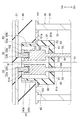
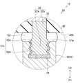
- FIG. 3 is an enlarged view of III shown in FIG. It is an IV enlarged view shown in FIG.
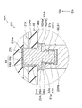
- It is a figure which shows the cross section around the terminal of the substrate structure in 2nd Embodiment.
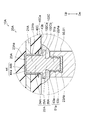
- It is a figure which shows the cross section around the terminal of the substrate structure in 3rd Embodiment.
- It is a figure which shows the cross section around the terminal of the substrate structure in 4th Embodiment.
- top and bottom refer to the top and bottom based on the state in which the wafer is placed on the substrate structure. Further, in the figure, Up is shown above and Dn is shown below. It should be noted that each of the drawings to be referred to is schematically shown, and details may be omitted.
- the cross-sectional view is exemplified only in the line II-II of FIG.
- the other cross sections shown in FIG. 2 having different directions around the straight line Li may be the same as the cross section on the line II-II or may be inferred from the cross section on the line II-II as long as there is no contradiction.
- the wafer mounting device 10 includes a base structure 20 on which an object (for example, a wafer) is placed, a power supply unit 11 that supplies electric power to the base structure 20, and power supply in the power supply unit 11. It has a control unit 13 for controlling the above.
- the base structure 20 includes a tubular hollow member 30, a base 40 joined to the hollow member 30 on which an object is placed, a conductor 21 located in the base 40, and at least a part of the base 40. Is located and the terminal 22 (metal body 22) connected to the conductor 21, the metal member 50 electrically connected to the conductor 21 via the terminal 22, and the base 40 while covering a part of the metal member 50. It has a cover 60 joined to the metal member 50 and a wiring unit 14 for electrically connecting the metal member 50 and the power supply unit 11.
- the hollow member 30 supports the substrate 40.
- the upper end of the hollow member 30 is joined to the lower surface of the base 40, and the lower end faces the direction away from the base 40.
- a cover 60 joined to the substrate 40 is located inside the tubular hollow member 30.
- the hollow member 30 is joined to the base 40 at a peripheral position where the cover 60 is joined to the base 40.
- the hollow member 30 houses the cover 60.
- the shape of the hollow member 30 is arbitrary.
- the hollow member 30 has, for example, a through hole, and the hollow portion has a cylindrical shape.
- the hollow member 30 has, for example, a through hole, and the hollow portion has a shape formed by a polygonal pillar such as a square pillar.
- the plan view shape for example, it may have a circular shape, an elliptical shape, or a polygonal shape such as a rectangular shape.
- the material of the hollow member 30 is arbitrary.
- the material of the hollow member 30 is, for example, insulating ceramics.
- the material of the hollow member 30 is, for example, a conductive material (metal).
- the shape of the hole located at the center of the hollow member 30 is arbitrary.
- the hollow member 30 connects the upper surface portion 31 facing the lower surface of the substrate 40, the lower surface portion 32 located on the opposite side of the upper surface portion 31, and the upper surface portion 31 and the lower surface portion 32, and the inner surface of the hollow member 30. It has an inner surface portion 33 that constitutes the above, and an outer surface portion 34 that connects the upper surface portion 31 and the lower surface portion 32 and constitutes the outer surface of the hollow member 30.
- the inner surface portion 33 and the outer surface portion 34 are along a straight line Li extending from each other in the thickness direction of the substrate 40.
- the inner surface portion 33 and the outer surface portion 34 may be inclined with respect to the straight line Li extending in the thickness direction of the substrate 40.
- the hollow member 30 may have a passage (not shown) for introducing a fluid into the flow path in the substrate 40 described later.
- a fluid consisting of a gas or a liquid passes through the passage.
- the shape and size of the passage can be set as appropriate.
- an insulating joining material 101 (hereinafter, referred to as a first joining material 101) that joins the base 40 and the hollow member 30 may be located.
- the substrate 40 is bonded to the hollow member 30 by the first bonding material 101.
- the first bonding material 101 may be located between the lower surface of the substrate 40 and the upper surface portion 31, may be located at a position where the lower surface of the substrate 40 and the inner surface portion 33 are in contact with each other, or the lower surface of the substrate 40. And may be located at a position in contact with the outer surface portion 34.
- the location where the first bonding material 101 is located may be a combination of two or more as described above.
- the first bonding material 101 is located at the boundary between the substrate 40 and the hollow member 30 over the entire circumferential direction.
- the first bonding material 101 can be paraphrased as an insulating bonding material.
- the thickness (vertical direction) of the first bonding material 101 is arbitrary.
- the thickness of the first bonding material 101 may be, for example, 1 mm or more, 3 mm or more, 5 mm or more, or 10 mm between the substrate 40 and the upper surface portion 31. It may be more than or equal to 15 mm or more. Further, the thickness of the first bonding material 101 may be smaller than 1 mm between the substrate 40 and the upper surface portion 31.
- the material of the first bonding material 101 is arbitrary.
- the material of the first bonding material 101 may be, for example, glass.
- the first bonding material 101 is a glass layer.
- the glass is made of, for example, silicate glass or crystallized glass.
- the first bonding material 101 may be a bonding material (adhesive material) other than glass.
- a bonding material adheresive material
- a compound containing Al 2 O 3 , Ca O and Y 2 O 3 as main components may be used. By containing these as main components, the coefficient of thermal expansion of the compound becomes close to the coefficient of thermal expansion of the substrate 40 (when the substrate 40 is ceramics).
- the resistance to halogen-based corrosion gas used in the production of semiconductors and the like can be improved.
- the contents of Al 2 O 3 , Ca O and Y 2 O 3 may be appropriately set.
- the first bonding material 101 may be two layers of a glass layer and a material other than glass. It can be said that the first bonding material 101 is an insulating bonding material.
- the lower surface portion 32 of the hollow member 30 may be connected to another part (not shown).
- a joining material (same or different joining material as the first joining material 101) may be positioned between the lower surface portion 32 and the other part.
- the hollow member 30 and the separate parts may be fixed by, for example, screwing.
- the substrate 40 is an insulating material such as ceramics.
- the ceramics constituting the substrate 40 are, for example, aluminum nitride (AlN), aluminum oxide (Al 2 O 3 , alumina), silicon carbide (SiC), and silicon nitride (Si 3 N 4 ). Etc. as the main component.
- the substrate 40 is a sintered body (aluminum nitride ceramics) containing aluminum nitride as a main component.
- the main component referred to here is, for example, a component that accounts for 50% by mass or more or 80% by mass or more of 100% by mass of all the components constituting the substrate 40.
- the substrate 40 is a flat plate-like substrate having thicknesses at the top and bottom.
- the shape of the substrate 40 is arbitrary.
- the shape of the substrate 40 may be circular, elliptical, rectangular, trapezoidal or the like in a plan view.
- the size of the substrate 40 is arbitrary.
- the dimensions of the substrate 40 are, for example, a diameter (for example, a circle-equivalent diameter when the shape in a plan view is not circular) is 20 cm or more and 40 cm or less, and a thickness is 5 mm or more and 35 mm or less.
- the substrate 40 has a first surface 41 on which an object is placed, a second surface 42 forming a surface opposite to the first surface 41, and the second surface 42 toward the first surface 41. It has a dent 43 and a dent 43.
- the first surface 41 constitutes the upper surface of the base 40
- the second surface 42 constitutes the lower surface of the base 40.
- the first surface 41 and the second surface 42 are parallel to each other.
- the recess 43 is located inside the hollow member 30, and has a polygonal shape such as a circular shape, an elliptical shape, or a rectangular shape in a cross section parallel to the first surface 41, for example.
- the recess 43 is connected to a third surface 43a extending from the second surface 42 toward the first surface 41 and the third surface 43a to form the bottom of the recess 43. It has a fourth surface 43b.
- the length of the third surface 43a is arbitrary, and may be 1/2 or more or 1/4 or more of the thickness of the substrate 40 in the vertical direction. , 1/8 or more in size. Further, the length of the third surface 43a may be smaller than 1/8 with respect to the thickness of the substrate 40 described above. In the example shown in FIG. 3, the third surface 43a extends along the straight line Li.
- the third surface 43a In the region surrounded by the third surface 43a, a portion located outside the base 40 of the terminal 22 is located. That is, it can be said that the third surface 43a surrounds a portion of the terminal 22 located outside the base 40. Further, the upper end of the metal member 50 is located in the region surrounded by the third surface 43a. That is, it can be said that the third surface 43a surrounds the upper end of the metal member 50 connected to the terminal 22.
- the fourth surface 43b is perpendicular to the straight line Li.
- the substrate 40 may have a flow path inside through which a fluid for cooling the mounted wafer and / or a fluid heated by a resistance heating element described later passes.
- the shape and size of the flow path can be appropriately changed according to the purpose of use of the flow path. That is, the shape and size of the flow path can be determined by various types of fluids consisting of gas or liquid, which are flowed according to the purpose of use.
- the conductor 21 may be a resistance heating element that generates heat by the electric power from the power supply unit 11. The heat generated by the resistance heating element heats the wafer placed on the first surface 41. That is, it can be said that the substrate structure 20 is a heater.
- the conductor 21 is made of, for example, a coil or a layered conductor.
- the conductor 21 is connected (directly connected) to the upper surface of the terminal 22.
- the conductor 21 may be connected to the side surface of the terminal 22.
- the conductor 21 has a spiral shape or a mianda shape, for example, in a plan view of the substrate 40.
- FIG. 2 shows an example in which the layered conductor 21 extends in a spiral shape or a meander shape, and the conductor 21 is shown in a cross section orthogonal to the extending direction (cross section along the width direction of the conductor 21). ..
- the conductor 21 may extend over the entire area of the substrate 40 along the first surface 41. As a result, the temperature of the entire first surface 41 can be efficiently raised.
- the conductor 21 is, for example, a metal made of Ni, W, Mo, Pt, or the like, or an alloy containing at least a part thereof.
- Such a conductor 21 can be positioned in the substrate 40 by, for example, screen printing the substrate before sintering and firing the substrate.
- the conductor 21 can be positioned in the substrate 40 by using a method such as CVD, vapor deposition, or sputtering.
- the substrate structure 20 may have one or more conductors 21. In other embodiments, the substrate structure 20 may have two or more conductors 21. When the base structure 20 has two conductors 21, the materials of these conductors 21 may be different from each other. The two conductors 21, 21 may differ in length and / or thickness. The resistance values of the two conductors 21 and 21 may be different from each other.
- the terminal 22 may be a metal (bulk material) having a predetermined length in the thickness direction of the substrate 40.
- the terminal 22 is, for example, a metal made of Ni, W, Mo, Pt, or the like, or an alloy containing at least a part thereof.
- the shape of the terminal 22 is arbitrary.
- the terminal 22 has, for example, a circular shape, a rectangular shape, a pentagonal shape, or the like in a cross section perpendicular to the direction in which the terminal 22 extends.
- the terminal 22 has a first portion 22a facing the outside of the substrate 40 and a second portion 22b located inside the substrate 40 and in contact with the conductor 21.
- the first portion 22a may occupy 15% or more, 35% or more, 50% or more, or 50% or more of the total volume of the terminal 22. It may occupy 65% or more.
- the ratio of the first portion 22a to the entire terminal 22 may be smaller than 15%.
- the first portion 22a may be entirely located within the substrate 40. When the entire first portion 22a is located inside the substrate 40, only the lower end of the first portion 22a is exposed to the outside of the substrate 40, and the lower end faces the outside of the substrate 40.
- the first portion 22a is connected to the metal member 50.
- the surface of the first portion 22a may have a screw shape. Further, the terminal 22 may be screwed into the metal member 50 having a screw shape. As another aspect, the surface of the first site 22a may be, for example, smooth.
- the surface of the second portion 22b may be smooth.
- the surface of the second portion 22b may have a screw shape. Since the surface of the second portion 22b has a screw shape, the contact area of the second portion 22b with respect to the substrate 40 increases. As a result, the terminal 22 is firmly fixed to the substrate 40 as compared with the case where the surface of the second portion 22b is smooth.
- the upper surface of the second portion 22b may be connected to the lower surface of the conductor 21 (example of FIG. 3), and the side surface (outer peripheral surface) thereof is connected to the side surface of the conductor 21 or the inner peripheral surface of the hole of the conductor 21. It may be (see FIG. 5 described later).
- the substrate structure 20 can have a plurality (two or more) of terminals 22.
- the substrate structure 20 has two terminals 22.
- the number of terminals 22 included in the substrate structure 20 may be one.
- the metal member 50 has a length extending from the upper end (first end) to the lower end (second end).
- the upper end side of the metal member 50 is connected to the terminal 22 and is covered with a cover 60.
- the lower end side of the metal member 50 is located outside the cover 60.
- the metal member 50 is, for example, a metal made of Cu, Fe, Al, Ag, Ni, W, Mo, Pt, or the like, or an alloy containing at least a part thereof.
- the alloy stainless steel containing Fe as a main component can be mentioned.
- the type of metal or alloy can be appropriately set from the viewpoint of cost, durability, and the like.
- the metal may be an alloy containing Ni or Pt.
- Ni plating or Pt plating can be applied to the surface of the metal member 50.
- the metal member 50 includes a connection portion 51 that constitutes the upper end side of the metal member 50 and is connected to the terminal 22, and the metal member 50 that extends from the connection portion 51 to the side opposite to the base 40. It has an extending portion 52 that constitutes the lower end side.
- the connecting portion 51 includes an A surface 51a forming the upper end of the connecting portion 51, a B surface 51b located on the opposite side of the A surface 51a and forming the lower end of the connecting portion 51, and A. It has a recess 51c (reference numeral is FIG. 4) that is recessed from the surface 51a toward the B surface 51b.
- the A surface 51a is bonded to the substrate 40. From these facts, it can be said that the metal member 50 is bonded to the substrate 40 around the terminal 22.
- the recess 51c is located on the A surface 51a and faces the first portion 22a of the terminal 22 together with the A surface 51a. Further, the recess 51c covers the first portion 22a. From this, it can be said that the metal member 50 (upper end side of the metal member 50) covers the first portion 22a from the outside of the substrate 40.
- the shape of the recess 51c is arbitrary.
- the recess 51c has a polygonal shape such as a circular shape, an elliptical shape, or a rectangular shape in a plan view.
- the inner diameter of the recess 51c is slightly larger than the outer diameter of the first portion 22a.
- the recess 51c may have, for example, a rectangular shape, a trapezoidal shape, a semicircular shape, a semi-elliptical shape, or the like in the vertical cross section of the metal member 50.
- the recess 51c has an inner wall 53a extending from the A surface 51a toward the B surface 51b and a bottom portion 53b connected to the lower portion of the inner wall 53a and forming the bottom of the recess 51c.
- the inner wall 53a may have a screw shape on its surface. To reiterate, the inner wall 53a having a screw shape on the surface may be screwed into the first portion 22a having a screw shape. Further, the inner wall 53a may be smooth. The inner wall 53a may be parallel to the straight line Li or may be tilted by a predetermined angle with respect to the straight line Li.
- the bottom portion 53b is a surface (part) that is located on the B surface 51b side of the elements constituting the recess 51c and faces the fourth surface 43b of the substrate 40.
- the bottom 53b may be parallel to the first surface 41.
- the bottom 53b may be tilted by a predetermined angle with respect to the first surface 41.
- the recess 51c can be easily formed by pressing a rotating body or the like against the bottom portion 53b.
- the extending portion 52 extends downward from the lower end of the connecting portion 51.
- the diameter of the extending portion 52 is smaller than the diameter of the connecting portion 51, for example.
- the diameter of the extending portion 52 may be, for example, 1/2 or less, 1/4 or less, or 1/8 or less with respect to the diameter of the connecting portion 51. You may.
- the diameter of the extending portion 52 may be larger than 1/2 with respect to the diameter of the connecting portion 51, for example.
- the diameter of the extending portion 52 may be the same as the diameter of the connecting portion 51.
- the lower end of the extending portion 52 may be located above the center of the hollow member 30. In another aspect, the lower end of the extending portion 52 may be located below the center of the hollow member 30. Further, the lower end of the extending portion 52 may be located below the lower end of the hollow member 30. In this case, the substrate structure 20 may have a structure in which the extending portion 52 is directly connected to the power supply portion 11.
- a metal layer 23 that connects the terminals 22 and the connecting portion 51 so as to be energized may be located.
- the metal layer 23 is, for example, a metal made of Cu, Fe, Al, Ag, Ni, W, Mo, Pt, or the like, or a metal containing at least a part thereof.
- the type of metal or alloy can be appropriately set from the viewpoint of cost, durability, and the like.
- the metal is Ni or Pt
- the durability of the metal layer 23 can be improved from the viewpoint of oxidation resistance.
- the durability of the substrate structure 20 is improved.
- the metal layer 23 may be an alloy containing Ni or Pt.
- the metal layer 23 may be located in the recess 51c, for example. More specifically, the metal layer 23 may be located, for example, between the terminal 22 and the bottom 53b and at least one between the terminal 22 and the inner wall 53a.
- the metal layer 23 includes, in addition to, or in place of, a portion located outside the recess 51c, between the terminal 22 and the bottom 53b and between the terminal 22 and the inner wall 53a. It may be.
- an insulating bonding material 102 (hereinafter, referred to as a second bonding material 102) may be located between the substrate 40 and the connecting portion 51.
- the second bonding material 102 is located between the substrate 40 and the A surface 51a on the substrate 40 side of the metal layer 23.
- the second bonding material 102 and the metal layer 23 are located in this order in the downward direction (direction from the base 40 to the terminal 22) from the first surface 41 (see FIG. 2).
- the second bonding material 102 may be located at a position other than the base 40 and the A surface 51a (for example, a position in contact with the side surfaces of the base 40 and the connecting portion 51).
- the second bonding material 102 may be located at a position formed by a combination of the two or more. From another viewpoint, the second bonding material 102 has a size of a gap between the A surface 51a and the surface of the base 40 facing the A surface 51a (the fourth surface 43b, which is the bottom surface of the recess 43 in the illustrated example). It may have the same thickness as the vertical direction), or may have a thickness larger than the thickness.
- the second bonding material 102 may be located between the first portion 22a (terminal 22) and the connecting portion 51 over the entire circumferential direction, and may seal the first portion 22a (terminal 22). ..
- the connecting portion 51 may cover the terminal 22 from the outside of the base 40 and may be joined to the base 40 around the terminal 22 to seal the terminal 22.
- At least a part of the second bonding material 102 may or may not be in contact with the metal layer 23.
- the second bonding material 102 may cover the metal layer 23 together with the substrate 40. Thereby, the airtightness of the metal layer 23 can be improved.
- the material of the second bonding material 102 is arbitrary.
- the second bonding material 102 is glass.
- the glass for example, silicate glass, crystallized glass and the like can be adopted.
- the second bonding material 102 is glass, it can be said that the second bonding material 102 is a glass layer.
- the second bonding material 102 may be a bonding material (adhesive) other than glass.
- a compound containing Al 2 O 3 , Ca O and Y 2 O 3 as main components may be used. By containing these as main components, the coefficient of thermal expansion of the compound becomes close to the coefficient of thermal expansion of the substrate 40 (when the substrate 40 is ceramics).
- the resistance to halogen-based corrosion gas used in the production of semiconductors and the like can be improved.
- the contents of Al 2 O 3 , Ca O and Y 2 O 3 may be appropriately set.
- the second bonding material 102 may be two layers of a glass layer and a material other than glass.
- the components of the second bonding material 102 may be the same as or different from the components of the first bonding material 101. It can be said that the second bonding material 102 is an insulating bonding material.
- the two connecting portions 51 and 51 are joined to the base 40 in a state of being connected to the two terminals 22 and 22, respectively.
- the two connecting portions 51 and 51 are joined to the substrate 40 via the second joining member 102, respectively.
- the component of the second joining member 102 that joins one connecting portion 51 may be the same as the component of the second joining member 102 that joins the other connecting portion 51, or the other connecting portion 51. It may be different from the component of the second joining material 102 that joins.
- the cover 60 See FIG.
- the cover 60 has a box shape with an open top.
- the cover 60 is fitted in the recess 43 constituting the base 40. Since the cover 60 is fitted in the recess 43, it can be said that the region SP inside the cover 60 is a closed space SP.
- the shape of the cover 60 is arbitrary.
- the cover 60 may have, for example, a cylindrical shape or a cubic shape in appearance.
- the shape of the cover 60 in a plan view may be, for example, a circular shape, an elliptical shape, or a polygonal shape such as a rectangular shape.
- the cover 60 may have a rectangular shape, a semicircular shape, a semi-elliptical shape, or a trapezoidal shape in a lateral view.
- the first portion 22a terminal 22
- the second bonding material 102 the connecting portion 51, and the metal layer 23 are located in the space SP sealed by the cover 60.
- the space SP sealed by the cover 60 may be filled with, for example, an inert gas. As a result, oxygen is suppressed from being contained in the space SP sealed by the cover 60.
- the inside of the space SP sealed by the cover 60 may be, for example, a vacuum.
- the cover 60 has a box-shaped thick portion 61 having an open upper surface and a thin portion 62 protruding from the upper surface of the thick portion 61 toward the substrate 40. .. Further, the cover 60 has a recess 63 that goes from the opening portion of the thin wall portion 62 to the thick wall portion 61 and constitutes the inner surface of the cover 60.
- the thick portion 61 is thicker than the thin portion 62.
- the outer diameter of the cover 60 differs in the vertical direction with the boundary between the thick portion 61 and the thin portion 62 as a boundary.
- the outer diameter of the thick portion 61 is larger than the outer diameter of the thin portion 62.
- the outer surface (outer surface) of the cover 60 has a bend.
- the inner diameter of the thick portion 61 and the inner diameter of the thin portion 62 are the same as each other. However, the two may be different.
- the thick portion 61 includes a first cover surface 61a that constitutes the upper surface of the thick portion 61 and is connected to the thin portion 62, a second cover surface 61b that extends in the direction from the first cover surface 61a, and the first cover surface 61b. It has a third cover surface 61c that is connected to the cover surface 61b and forms the lower surface of the thick portion 61, and an insertion hole 64 that opens at least a part of the third cover surface 61c.
- the first cover surface 61a faces the substrate 40. There is a gap between the first cover surface 61a and the substrate 40.
- the size of this interval may be, for example, 0.1 mm or more, 0.5 mm or more, 1 mm or more, or smaller than 0.1 mm.
- the third bonding material 103 which will be described later, is located within the above interval. There may not be a gap between the first cover surface 61a and the substrate 40.
- the cover 60 has two insertion holes 64 and 64 (at least a part of the cover 60 has an insertion hole 64). Extension portions 52 and 52 pass through the two insertion holes 64 and 64, respectively.
- the number of insertion holes 64 is arbitrary and may be one or three or more.
- the size of this interval may be, for example, 0.1 mm or more, 0.5 mm or more, 1 mm or more, or smaller than 0.1 mm.
- the fourth joint member 104 which will be described later, is located within the above interval.
- the thin portion 62 has a fourth cover surface 62a facing the recess 43 of the base 40, and a fifth cover surface 62b connecting the fourth cover surface 62a and the first cover surface 61a.
- the shape of the recess 63 is arbitrary, and in the vertical cross section of the cover 60, for example, a rectangular shape, a semicircular shape, a semi-elliptical shape, a trapezoidal shape, or the like is exhibited.
- the opening portion of the recess 63 faces the base 40, and in the sealed space SP surrounded by the base 40 and the recess 63, the first portion 22a (terminal 22), the second bonding material 102, the connecting portion 51, and the metal layer 23 are provided. Is located.
- the metal member 50 that positions the connecting portion 51 in the recess 63 has the lower end side (extending portion 52) positioned outside the cover 60 through the insertion hole 64.
- a bonding material 103 (hereinafter, referred to as a third bonding material 103) is located between the substrate 40 and the first cover surface 61a.
- the third bonding material 103 may be located at a position where the base 40 and the second cover surface 61b are in contact with each other, or may be located at a position where the base 40 and the fifth cover surface 62b are in contact with each other. May be good. Further, the third bonding material 103 may be located at a position where two or more of the above three places are combined.
- the third bonding material 103 has the cover 60 bonded to the substrate 40.
- the third bonding material 103 may be located, for example, between the substrate 40 and the cover 60 over the entire circumferential direction.
- the material of the third bonding material 103 is arbitrary.
- the third bonding material 103 is glass.
- the glass for example, silicate glass, crystallized glass and the like can be adopted.
- the third bonding material 103 is glass, it can be said that the third bonding material 103 is a glass layer.
- the third bonding material 103 may be a bonding material (adhesive) other than glass.
- a compound containing Al 2 O 3 , Ca O and Y 2 O 3 as main components may be used. By containing these as main components, the coefficient of thermal expansion of the compound becomes close to the coefficient of thermal expansion of the substrate 40 and the cover 60 (when the substrate 40 and the cover 60 are ceramics).
- the resistance to halogen-based corrosion gas used in the production of semiconductors and the like can be improved.
- the contents of Al 2 O 3 , Ca O and Y 2 O 3 may be appropriately set.
- the third bonding material 103 may be two layers of a glass layer and a material other than glass.
- the components of the third bonding material 103 may be the same as or different from the components of the first bonding material 101 and / or the second bonding material 102. It can be said that the third bonding material 103 is an insulating bonding material.
- a joining material 104 (hereinafter, referred to as a fourth joining material 104) is located between the extending portion 52 and the inner surface of the insertion hole 64.
- the fourth joining member 104 may be located at a position where the third cover surface 61c and the extending portion 52 are in contact with each other, or a portion where the recess 63 (for example, the bottom surface thereof) is in contact with the extending portion 52. It may be located in. Further, the fourth bonding material 104 may be located at a position where two or more of the above three places are combined. The fourth joining member 104 fills the space between the extending portion 52 and the inner surface of the insertion hole 64.
- the material of the fourth bonding material 104 is arbitrary.
- the fourth bonding material 104 is glass.
- the glass for example, silicate glass, crystallized glass and the like can be adopted.
- the fourth bonding material 104 is glass, it can be said that the fourth bonding material 104 is a glass layer.
- the fourth bonding material 104 may be a bonding material (adhesive) other than glass.
- a compound containing Al 2 O 3 , Ca O and Y 2 O 3 as main components may be used. By containing these as main components, the coefficient of thermal expansion of the compound becomes close to the coefficient of thermal expansion of the substrate 40 (when the substrate 40 is ceramic and the metal member 50 is tungsten W).
- the fourth bonding material 104 may be two layers of a glass layer and a material other than glass.
- the components of the fourth bonding material 104 may be the same as or different from the components of the first bonding material 101 and / or the second bonding material 102.
- the components of the fourth bonding material 104 may be the same as or different from the components of the third bonding material 103. It can be said that the third bonding material 103 is an insulating bonding material.
- the fourth bonding material 104 can also be called a bonding layer together with the first to third bonding materials 101, 102, 103.
- the airtightness of the region SP (sealed space SP) surrounded by the recess 63 is further improved. Further, for example, by closing the space between the base 40 and the cover 60 over the entire circumferential direction, for example, the airtightness of the region SP surrounded by the recess 63 can be further improved. Further, for example, by closing the space between the metal member 50 and the cover 60 over the entire circumferential direction, the airtightness of the region SP surrounded by the recess 63 can be further improved.
- the upper end of the wiring unit 14 is connected to the metal member 50, and the lower end is connected to the power supply unit 11.
- the wiring portion 14 may be entirely located in the hollow member 30, or may be partially located in the hollow member 30.
- the power supply unit 11 is located outside the substrate 40 and supplies electric power to the conductor 21 (for example, a resistance heating element) via the wiring unit 14.
- the power supply unit 11 is electrically connected to the conductor 21 via the wiring unit 14.
- the power supply unit 11 includes a power supply circuit that converts the electric power supplied from the power source into electric power having an appropriate voltage and supplies the electric power to the conductor 21.
- Control unit 13 controls the supply of electric power to the conductor 21 in the power supply unit 11. For example, when the control unit 13 controls the power supply unit 11, the resistance heating element generates heat. The heat generated by the resistance heating element heats the object placed on the first surface 41.
- the base structure 20 has at least a region SP surrounded by the base 40 and the recess 63 of the cover 60.
- a terminal 22 connected to the first end side of the metal member 50 is located in the region SP surrounded by the base 40 and the recess 63. Therefore, it can be said that the terminal 22 is located in the region SP surrounded by the substrate 40 and the recess 63.
- the entry of external air (for example, oxygen) into the space where the terminal 22 is located is reduced.
- contact with the terminal 22 oxygen is suppressed. Therefore, the substrate structure 20 has durability.
- the area SP is surrounded by the cover 60, it can be said that the area SP is a closed space SP sealed by the cover 60. Since the region SP is a space, it is possible to suppress the application of thermal stress due to the temperature change in the region SP. As a result, it is possible to suppress the load applied to the terminal 22.
- the base structure 20 may accommodate the cover 60 and may further have a hollow member 30 joined to the base 40 around the joint position between the cover 60 and the base 40.
- the terminal 22 is doubly surrounded by the hollow member 30 together with the cover 60.
- the airtightness of the terminal 22 located in the cover 60 can be further improved. Therefore, the durability of the substrate structure 20 is improved.
- the substrate 40 may have a recess 43.
- the cover 60 has a thin-walled portion 62 fitted in the recess 43 and a thick-walled portion 61 connected to the thin-walled portion 62 and partially facing the substrate 40.
- the base 40 and the cover 60 are fixed in close contact with each other.
- the bonding material can be positioned between the base 40 and the thick portion 61. As a result, the durability of the substrate structure 20 is improved.
- the metal member 50 may cover the first portion 22a of the terminal 22. By covering the first portion 22a with the metal member 50, the airtightness of the terminal 22 can be further improved. Therefore, the durability of the substrate structure 20 is improved.
- the terminal 22 is sealed at the same time as the metal member 50 is attached in the assembly work of the base structure 20. You will be able to do it. Further, it is not necessary to prepare a separate component for sealing the terminal 22. As a result, the efficiency of the assembling work of the substrate structure 20 can be improved, and the increase in the number of parts can be suppressed.
- the metal member 50 may have a recess 51c on the first end side, and the first portion 22a may be covered with the recess 51c of the metal member 50. Since the first portion 22a is covered with the recess 51c, the airtightness of the terminal 22 is further improved. As a result, the durability of the substrate structure 20 is improved.
- the substrate structure 20 may have a glass layer 102 that is in contact with each of the metal layer 23 and the substrate 40 and covers the metal layer 23 together with the substrate 40. Since the metal layer 23 is covered with the glass layer 102 together with the substrate 40, the metal layer 23 is in a sealed state. As a result, the metal layer 23 is suppressed from being exposed to the outside air. As a result, oxidation of the metal layer 23 is suppressed. Therefore, the durability of the substrate structure 20 is improved.
- the substrate structure 20 may have a metal member 50 that is connected to the terminal 22 from the outside of the substrate 40 while covering the first portion 22a, and is joined to the substrate 40 to seal the terminal 22. ..
- a metal member 50 that is connected to the terminal 22 from the outside of the substrate 40 while covering the first portion 22a, and is joined to the substrate 40 to seal the terminal 22. ..
- the terminal 22 is connected to the metal member 50 while being covered (sealed) by the metal member 50, the terminal 22 is connected to the metal member 50 at the same time as the metal member 50 is attached in the assembly work of the base structure 20. Can be sealed. Further, it is not necessary to prepare a separate component for sealing the terminal 22. As a result, the efficiency of the assembling work of the substrate structure 20 can be improved, and the increase in the number of parts can be suppressed.
- the substrate structure 20 may be a heater in which the conductor 21 is a resistance heating element. As a result, the substrate structure 20 can directly heat the placed object. As a result, the substrate structure 20 can raise the temperature of the object faster.
- the terminal 22 is located in the sealed space SP, oxygen is suppressed from coming into contact with the high temperature terminal 22 when heating the object. As a result, the heater is durable.
- the wafer mounting device 10 includes the above-mentioned substrate structure 20. As a result, the wafer mounting device 10 has durability.
- FIG. 5 is a diagram showing a second embodiment in the present disclosure, and corresponds to FIG. 4 above.
- the substrate structure 20A in the second embodiment is mainly different in that the terminal 22A has a collar portion 25A and that the metal layer 23A is provided around the terminal 22A in relation to the first embodiment. ing.
- Other specific structures for example, the cover 60, etc.
- reference numerals are used and detailed description thereof will be omitted.
- matters not particularly mentioned are the same as those of the embodiments described above, or have been described above. It may be inferred from the embodiment.
- the conductor 21A is in contact with the metal layer 23A described later.
- the conductor 21A is connected to the terminal 22A via the metal layer 23A.
- the terminal 22A has a shaft-shaped portion 24A whose upper end side is located inside the base 40 and whose lower end side is located outside the base 40, a protruding portion 26A protruding from the lower end of the shaft-shaped portion 24A toward the connecting portion 51, and the outside of the base 40. It has a flange portion 25A protruding from the side surface of the shaft-shaped portion 24A toward the side.
- the terminal 22A can be distinguished into a first portion 22Aa located outside the substrate 40 and a second portion 22Ab located inside the substrate 40.
- the first portion 22Aa is a portion constituting a part (lower end side) of the shaft-shaped portion 24A, the protruding portion 26A, and the flange portion 25A.
- the second portion 22Ab is a portion constituting the remaining portion (upper end side) of the shaft-shaped portion 24A.
- the protruding portion 26A has a screw shape at least a part of the surface thereof, and may be screwed into the recess 51c of the metal member 50.
- the protruding portion 26A may have a smooth surface and may be joined to the metal member 50 by a metal layer 23 described later.
- the flange portion 25A protrudes from the protruding portion 26A in the direction intersecting the straight line Li.
- the flange portion 25A may project in a direction perpendicular to the straight line Li, for example.
- the flange portion 25A may project so that the inclination angle with respect to the straight line Li is 60 ° or less, or the inclination angle with respect to the straight line Li may be 45 ° or less, for example.
- At least a part of the collar portion 25A is bonded to the substrate 40, for example. Since the collar portion 25A protrudes from the shaft-shaped portion 24A constituting the first portion 22Aa, it can be said that the collar portion 25A protrudes from the first portion 22Aa.
- a conductive metal layer 23Aa containing at least a metal (hereinafter, may be referred to as a first metal layer 23Aa) is located between the substrate 40 and the terminal 22A.
- the first metal layer 23Aa connects the conductor 21A and the terminal 22A so as to be energized.
- the recess into which the terminal 22A of the substrate 40 is inserted is defined as the terminal recess 44.
- the first metal layer 23Aa may be located between the inner peripheral surface 44a of the terminal recess 44 and the shaft-shaped portion 24A, and / or the bottom surface 44b of the terminal recess 44 and the shaft-shaped portion 24A. It may be located in between.
- first metal layer 23Aa may be located between the surface on which the terminal recess 44 is open (the fourth surface 43b, which is the bottom surface of the recess 43 in the illustrated example) and the upper surface of the flange portion 25A. .. From another aspect, the first metal layer 23Aa may be interposed between the side surface of the terminal 22A and the inner surface (or side surface) of the hole of the conductor 21 to contribute to the connection between the two (illustrated example). It may be interposed between the upper surface of the terminal 22A and the lower surface of the conductor 21 to contribute to the connection between the two.
- the first metal layer 23Aa may have a function as a bonding material.
- the first metal layer 23Aa may be in close contact with the substrate 40 (and the conductor 21) and the terminal 22A, and may be bonded to each other.
- the first metal layer 23Aa is a conductive bonding material made of metal.
- the first metal layer 23Aa is located above the substrate-side bonding material 102Aa described later.
- a conductive metal layer 23Ab containing at least a metal (hereinafter, may be referred to as a second metal layer 23Ab) is located between the terminal 22A and the metal member 50.
- the second metal layer 23Ab connects the terminal 22A and the metal member 50 so as to be energized.
- the second metal layer 23Ab may be located between the A surface 51a and the flange portion 25A, may be located between the protruding portion 26A and the inner wall 53a, or may be located between the protruding portion 26A and the bottom portion 53b. It may be located in between. Further, the second metal layer 23Ab may be located at a location where two or more of the above three locations are combined.
- the second metal layer 23Ab may have a function as a bonding material.
- the second metal layer 23Ab may be in close contact with the terminal 22A and the metal member 50 to fix both.
- the second metal layer 23Ab is a conductive bonding material made of metal.
- the component of the second metal layer 23Ab may be the same as the component of the first metal layer 23Aa, or may be different from the component of the first metal layer 23Aa.
- a part of the second bonding material 102A (hereinafter, may be referred to as a substrate side bonding material 102Aa) is located between the substrate 40 and the terminal 22A. More specifically, the substrate-side bonding material 102Aa is located between the substrate 40 and the terminal 22A at a position below the first metal layer 23Aa so that the first metal layer 23Aa is sealed. At this time, the first metal layer 23Aa and the base-side bonding material 102Aa are located in this order in the downward direction (direction from the base 40 to the terminal 22A) from the first surface 41 (see FIG. 2).
- the first metal layer 23Aa is covered with the substrate 40, the terminals 22A, and the substrate-side bonding material 102Aa. As a result, the first metal layer 23Aa is sealed with the substrate side bonding material 102Aa together with the substrate 40 and the terminal 22A. As a result, the exposure of the metal layer 23 to the outside air is suppressed. Therefore, it is possible to provide a durable substrate structure 20A.
- the substrate-side bonding material 102Aa may be located between the substrate 40 and the terminal 22A over the entire circumferential direction. As a result, the first metal layer 23Aa is more reliably sealed.
- the substrate-side bonding material 102Aa may be located between the flange portion 25A and the substrate 40 (fourth surface 43b), or may be located between the shaft-shaped portion 24A and the substrate 40 (inner peripheral surface 44a). You may. Further, the substrate-side bonding material 102Aa may be located at a position formed by a combination thereof.
- the substrate side bonding material 102Aa (bonding material 102) is located between the substrate 40 and the flange portion 25A.
- the substrate-side bonding material 102Aa is located between the flange portion 25A and the substrate 40, it can be said that the flange portion 25A is bonded to the substrate 40. Since the flange portion 25A is bonded to the substrate 40, the terminal 22A is bonded to the substrate 40 more strongly than when the collar portion 25A is not bonded to the substrate 40.
- the substrate-side bonding material 102Aa is located between the flange portion 25A and the substrate 40, the flange portion 25A is not bonded to the substrate 40, so that the flange portion 25A is between the substrate 40 and the terminal 22A.
- the amount of the substrate-side bonding material 102Aa increases.
- the first metal layer 23Aa can be more reliably sealed.
- the airtightness of the first metal layer 23Aa can be further improved.
- the substrate-side bonding material 102Aa may or may not be in contact with the first metal layer 23Aa. Since the substrate-side bonding material 102Aa is in contact with the first metal layer 23Aa, the airtightness of the first metal layer 23Aa is further improved.
- the material of the substrate-side bonding material 102Aa is arbitrary.
- the substrate-side bonding material 102Aa is made of, for example, glass.
- the substrate-side bonding material 102Aa is made of glass, it can be said that the substrate-side bonding material 102Aa is a glass layer 102Aa. Since the substrate-side bonding material 102Aa is a glass layer, for example, the terminal 22A is fixed by the glass layer together with the first metal layer 23Aa.
- the glass layer has a large bonding force to the substrate 40, the terminal 22A, and the metal layer 23A (first metal layer 23Aa). As a result, the terminal 22A can be more firmly bonded to the substrate 40.
- the substrate-side bonding material 102Aa may be a bonding material (adhesive) other than glass.
- a compound containing Al 2 O 3 , Ca O and Y 2 O 3 as main components may be used.
- the coefficient of thermal expansion of the compound becomes close to the coefficient of thermal expansion of the substrate 40 (when the substrate 40 is ceramic and the terminal 22A and / or the metal member 50 is tungsten W).
- the resistance to halogen-based corrosion gas used in the production of semiconductors and the like can be improved.
- the contents of Al 2 O 3 , Ca O and Y 2 O 3 may be appropriately set.
- the remainder of the second bonding material 102A (hereinafter, may be referred to as the metal member side bonding material 102Ab) is located between the terminal 22A and the metal member 50.
- the metal member side bonding member 102Ab may be located between the terminal 22A and the metal member 50 over the entire circumferential direction. As a result, the second metal layer 23Ab is more reliably sealed.
- a part of the metal member side bonding member 102Ab may enter between the terminal 22A and the inner wall 53a.
- the metal member side bonding material 102Ab may or may not be in contact with the second metal layer 23Ab.
- the material of the metal member side bonding material 102Ab is arbitrary.
- the metal member side bonding material 102Ab is made of, for example, glass.
- the metal member side bonding material 102Ab is glass, it can be said that the metal member side bonding material 102Ab is a glass layer.
- the metal member side bonding material 102Ab may be a bonding material (adhesive) other than glass.
- the component of the metal member side bonding material 102Ab may be the same as the component of the substrate side bonding material 102Aa, or may be different from the component of the substrate side bonding material 102Aa.
- the substrate-side bonding material 102Aa may be a bonding material (adhesive) other than glass.
- a compound containing Al 2 O 3 , Ca O and Y 2 O 3 as main components may be used.
- the coefficient of thermal expansion of the compound becomes close to the coefficient of thermal expansion of the terminal 22A and / or the metal member 50 (when the terminal 22A and / or the metal member 50 is tungsten W).
- the resistance to halogen-based corrosion gas used in the production of semiconductors and the like can be improved.
- the contents of Al 2 O 3 , Ca O and Y 2 O 3 may be appropriately set.
- the metal member side bonding member 102Ab may be located between the lower surface of the flange portion 25A and the upper end of the metal member 50.
- the metal member side bonding member 102Ab may be located between the side surface of the protrusion 26A and the inner wall 53a.
- the metal member side joining material 102Ab is, for example, an insulating joining material, and joins the terminal 22A and the metal member 50. Further, the metal member side bonding material 102Ab is in contact with, for example, the second metal layer 23Ab, and seals the second metal layer 23Ab. As a result, the airtightness of the second metal layer 23Ab can be improved.
- the first metal layer 23Aa and the second metal layer 23Ab constitute the metal layer 23A corresponding to the first embodiment.
- FIG. 6 is a diagram showing a third embodiment in the present disclosure, and corresponds to FIG.
- the insulating joining material 102B extends over the entire fourth surface 43b (bottom surface) of the recess 43, and the joining material 102B covers the cover 60B and the base 40.
- the main difference is that it also contributes to the connection with.
- the bonding material 102B covers the entire fourth surface 43b.
- the fourth surface 43b covered with the bonding material 102B referred to here excludes a region where a recess such as a terminal recess 44 into which the terminal 22 is inserted is formed. Further, even though the entire fourth surface 43b is covered with the joining material 102B, the position where the joining material 102B cannot be arranged may not be covered with the joining material 102B. For example, in the illustrated example, a gap is formed between the cover 60B and the fourth surface 43b, but when the cover 60B has a portion that abuts on the fourth surface 43b, the fourth surface at the contact position is the fourth. The surface 43b may not be covered by the bonding material 102B.
- voids may be generated due to the viscosity of the bonding material 102B or the like.
- a relatively small gap may be formed in the vicinity of the corner formed by the fourth surface 43b and the third surface 43a, and the bonding material 102B may not cover the fourth surface 43b. Such a case is also included in the mode in which the entire fourth surface 43b is covered.
- the thickness of the bonding material 102B is different from the thickness of the bonding material 102 illustrated in FIG. 3, and the A surface 51a of the metal member 50 and the surface (recess 43) of the base 40 facing the A surface 51a. It is made larger than the size of the gap (vertical direction) with the fourth surface 43b) which is the bottom surface of the above.
- the joining member 102B is in contact with not only the A surface 51a but also the side surface of the metal member 50. Of course, the bonding material 102B may be in contact with only the A surface 51a of the metal member 50.
- the joining material 102B is also in contact with the cover 60B, and joins the cover 60B and the base 40 (contributing to the fixing of both). Further, the bonding material 102B may be in contact with the cover 60B and the base 40 over the entire circumferential direction of the cover 60B, and may contribute to sealing the sealed space SP. More specifically, in the example of FIG. 6, the upper surface (fourth cover surface 62a) of the cover 60B is the surface of the base 40 facing the fourth cover surface 62a (the fourth surface which is the bottom surface of the recess 43 in the illustrated example). It is far from 43b).
- the joining material 102B is in contact with the fourth cover surface 62a and also in contact with a part of the inner peripheral surface and the outer peripheral surface of the cover 60B. Unlike the illustrated example, the bonding material 102B may only be in contact with any one of the upper surface, the inner peripheral surface, and the outer peripheral surface of the cover 60B.
- the joining material 102B extends over the entire fourth surface 43b (bottom surface) of the recess 43, and joins the cover 60B and the base 40.
- the bonding material 102B extends over the entire fourth surface 43b (bottom surface)
- the cover 60B and the substrate 40 do not have to be bonded.
- the upper surface of the cover 60B (fourth cover surface 62a) may be separated from the fourth surface 43b of the substrate 40 with a gap larger than the thickness of the bonding material 102B.
- the joining material 102B may join the metal member 50 (and / or the terminal 22) and the base 40, and may join the cover 60B and the base 40 in a manner that does not spread over the entire fourth surface 43b. ..
- the terminal 22 of the first embodiment is illustrated, but the bonding material 102B of the present embodiment may be combined with the terminal 22A of the second embodiment.
- the thickness of the bonding material 102B at this time may be the thickness from the fourth surface 43b to the upper surface of the flange portion 25A, or the thickness from the fourth surface 43b to the middle of the outer peripheral surface of the collar portion 25A. It may be the thickness from the fourth surface 43b to the lower surface of the collar portion 25A, or may be the thickness from the fourth surface 43b to the lower surface of the collar portion 25A. , The thickness may reach the metal member 50 as in the present embodiment.
- the bonding material 102B may contribute to the bonding between the terminal 22 or 22A and the substrate 40, or may contribute to the bonding between the metal member 50 and the substrate 40. , It may contribute to both.
- the bonding material 102B may or may not be provided.
- the insulating bonding material 102B may come into contact with the bonding material 103, and in such a form, the bonding between the cover 60B and the base 40 becomes stronger and is sealed. Sex is obtained.
- the substrate 40 has a recess 43 and a terminal recess 44 (FIG. 5) that is open to the bottom surface (fourth surface 43b) of the recess 43. ,have. A part of the terminal 22 is inserted into the terminal recess 44. At least the first end (upper end) of the metal member 50 is housed in the recess 43. At least the opening portion (upper end portion) of the cover 60B is housed in the recess 43. Therefore, as in the other embodiments, the airtightness of the sealed space SP accommodating the terminal 22 and the metal member 50 is improved.
- the insulating bonding material 102B extends over the entire bottom surface (fourth surface 43b) of the recess 43. In this case, for example, heat dissipation from the fourth surface 43b can be reduced.
- the substrate structure is a heater, the heating efficiency of the wafer can be improved.
- the insulating joining material 102B joins the metal member 50 and the bottom surface (fourth surface 43b) of the recess 43, and also joins the cover 60B and the fourth surface 43b. ..
- the bonding material 102B between the fourth surface 43b and the cover 60B, heat dissipation from the fourth surface 43b to the cover 60B can be reduced.
- the substrate structure is a heater, the heating efficiency of the wafer can be improved.
- FIG. 7 is a diagram showing a fourth embodiment in the present disclosure, and corresponds to FIG.
- the base body side bonding material 102Ca and the metal member side bonding material 102Cb are connected to cover the flange portion 25A, and the bonding material 102C is a gap between the base body 40C.
- the main difference is that it penetrates into 40Ca. The difference between the two does not have to hold at the same time. Further, the point that the bonding material 102C enters the gap 40Ca may be applied to the first or third embodiment.
- the base-side bonding material 102Ca and the metal member-side bonding material 102Cb are connected, for example, over the entire circumferential direction of the terminal 22A. Therefore, the terminal 22A is entirely covered (sealed) with the substrate 40C, the metal member 50, and the bonding material 102C. Also in such an embodiment, the description of other embodiments may be incorporated with respect to the material of the bonding material 102C, the portion where the bonding material 102C contacts the metal member 50, and the like. In the illustrated example, the bonding material 102C covers only the periphery of the terminal recess 44 on the bottom surface (fourth surface 43b) of the recess 43, as in the first and second embodiments. However, as shown in the third embodiment, the bonding material 102C may spread over the entire fourth surface 43b or contribute to the bonding between the cover 60 and the base 40C.
- the gap 40Ca is open to the inner peripheral surface 44a of the terminal recess 44.
- the gap 40Ca extends along the first surface 41 (FIG. 1) of the substrate 40C, for example, and forms a layered space. From another viewpoint, the gap 40Ca extends in a vertical cross section as shown in FIG. 7 in a direction intersecting the insertion direction of the terminal 22A into the terminal recess 44.
- the shape of the gap 40Ca may be appropriately set.
- the gap 40Ca may expand around the terminal recess 44 in a plan view of the first surface 41, or may expand unevenly in a predetermined direction from the terminal recess 44.
- the gap 40Ca may have an appropriate planar shape such as a circle or a polygon.
- the height (length in the vertical direction) of the gap 40Ca may or may not be constant in the vertical cross section as shown in FIG. 7. As an example of the latter, there can be mentioned an aspect in which the height becomes smaller as the distance from the terminal recess 44 increases.
- the gap 40Ca is expressed as a layered space, but the gap 40Ca may have a shape that cannot be regarded as a layered space (a shape in which the lateral spread is smaller than the height).
- the height of the gap 40Ca (length in the vertical direction) and the length in the vertical cross section (length in the horizontal direction of the paper surface) may be appropriately set.
- the height of the gap 40Ca is relatively small, and in the illustrated example, it is smaller than the size of the gap between the terminal 22A and the inner peripheral surface 44a of the terminal recess 44 (in the left-right direction of the paper surface).
- the height of the gap 40Ca may be larger than the size of the latter gap.
- an example of the height of the gap 40Ca is 200 ⁇ m or less.
- the gap 40Ca may have the above-mentioned portion having a thickness of 200 ⁇ m or less over 50% or more, 80% or more, or the entire area of the gap 40Ca in a plan view. Further, the length of the gap 40Ca from the terminal recess 44 in the vertical cross section (or the maximum distance from the terminal recess 44 in the plan view to the outer edge of the gap 40Ca) is twice or more and five times or more the height of the gap 40Ca. Or 10 times or more.
- the gap 40Ca may be formed by an appropriate method. For example, when the substrate 40C is produced by firing a laminate of ceramic green sheets, the firing conditions are appropriately set, and the shrinkage of the sheets accompanying the firing is used to generate a gap 40Ca between the sheets. You can. Further, for example, by arranging a relatively small spacer between the sheets when laminating the ceramic green sheet, a gap 40Ca may be formed before firing, or a gap due to shrinkage during firing may be easily generated. ..
- the bonding material 102C is filled in the gap 40Ca.
- the filling rate may be appropriately set.
- the bonding material 102C may be filled in 50% or more of the volume of the gap 40Ca, or may be only filled in less than 50%. Further, the bonding material 102C is in contact with at least one of the lower surface and the upper surface of the gap 40Ca (both in the illustrated example).
- the substrate-side bonding material 102Ca located between the flange portion 25A and the substrate 40C is composed of an insulating material, and the insulating material (bonding material 102C) is the flange portion 25A. It reaches between the flange portion 25A and the metal member 50 via the outer peripheral surface of the flange portion 25A from between the substrate 40C and the base 40C. In this case, for example, heat dissipation from the collar portion 25A is reduced. As a result, the power supply efficiency is improved.
- the substrate 40C has a terminal recess 44 into which a part of the terminal 22A (second portion 22Ab) is inserted, and a gap 40Ca opened on the inner peripheral surface of the terminal recess 44. have.
- An insulating bonding material 102C is located between the terminal 22A and the inner peripheral surface 44a of the terminal recess 44 and in the gap 40Ca. In this case, for example, since the bonding material 102C is also located in the gap 40Ca, the adhesion between the bonding material 102C and the substrate 40C is improved, and the reliability of bonding is improved.
- FIG. 8 is a diagram showing a fifth embodiment in the present disclosure, and corresponds to FIG.
- the fifth embodiment can be regarded as a modification of the third embodiment.
- the description of the third embodiment may be incorporated for matters not particularly mentioned.
- the bonding material 102B spreads over the entire fourth surface 43b (bottom surface) of the recess 43.
- the joining material 102B of the third embodiment is divided in the direction along the fourth surface 43b, and becomes the joining material 102D and the joining material 103A.
- the dividing position is, for example, between the connecting portion 51 and the inner surface of the recess 63 of the cover 60.
- the bonding material 102D may be regarded as the same as the bonding material 102 of the first embodiment. Then, in addition to the joining material 102 of the first embodiment, a joining material 103A for joining the upper end of the cover 60B (the fourth cover surface 62a and its surroundings) and the base 40 is provided. The joining material 103A may be connected to the joining material 103 in the same manner as the joining material 102B of the third embodiment.
- At least one of the joint between the metal member 50 and the bottom surface (fourth surface 43b) of the recess 43 and the joint between the cover 60B and the bottom surface of the recess 43 is formed. It has the joining materials 102B and 103A of. Therefore, the airtightness around the terminal 22 and / or in the cover 60B is improved.
- the substrate is bonded to the hollow member via the first bonding material.
- the substrate may be integrally joined by firing.
- the materials of the first joint material to the fourth joint material can be arbitrarily set, and the materials of these joint materials can be the same.
- the temperature of the heat treatment for the first joint material to the fourth joint material at the time of assembling the substrate structure can be made the same.
- the manufacturing process can be simplified.
- the conductor which is a resistance heating element has been described.
- the conductor may be an electrostatic chuck that adsorbs the wafer on the first surface, or may be a high-frequency electrode used when generating plasma.
- the terminals may be arranged on the upper surface of the substrate, the side surface of the substrate, or the like.
- the place where the terminal is arranged is arbitrary.
- the substrate structure in which the first surface on which the wafer is placed is parallel to the second surface has been described.
- the first plane does not necessarily have to be parallel to the second plane.
- the substrate structure in which the substrate has a recess has been described.
- the substrate does not have to have a recess.
- the recess may not be located inside the hollow member or may not be fitted to the cover.
- the substrate structure in which the metal member has a recess on the upper end side has been described.
- the depression is not an essential component and may be eliminated if necessary.
- an example in which the first portion is covered with a depression has been described.
- the first portion may be covered with the protrusion. That is, there are at least two or more methods in which the metal member covers the terminal (first portion).
- the cover has a recess.
- the cover is not limited to the one having a recess.
- the cover may have a flat plate shape that closes the recess of the substrate.
- such a cover may have, for example, a notch cut out to a depth overlapping the recess of the substrate at the edge.
- the metal member may be extended from the notch.
- the substrate structure of the present disclosure can also mount an object other than the wafer.
- the wafer mounted on the substrate structure of the present disclosure is not limited to a semiconductor, and includes, for example, a crystal wafer.
Landscapes
- Chemical & Material Sciences (AREA)
- Engineering & Computer Science (AREA)
- Ceramic Engineering (AREA)
- Container, Conveyance, Adherence, Positioning, Of Wafer (AREA)
- Resistance Heating (AREA)
Abstract
基体構造体は、絶縁性の基体と、基体内に位置している導体と、少なくとも一部が基体内に位置して導体に電気的に接続されている端子と、を備えている。端子は、基体の外部に臨んでいる第1部位を有する。カバーは、凹部を有し、凹部の開口部分が基体に臨み、少なくとも一部に挿通孔を有する。金属部材は、第1端から第2端に亘る長さを有し、第1端側が端子に接続され、凹部内から挿通孔内に亘り、第2端がカバー外に位置している。少なくとも基体およびカバーの凹部により囲まれた領域は、密閉空間である。
Description
本開示は、基体構造体、および基体構造体を用いたウエハ載置装置に関する。
例えば、半導体を製造する半導体製造装置において、ウエハなどの対象物が載置される基体構造体が知られている。基体構造体としては、例えば、下記特許文献1に開示のセラミックヒータ、および下記特許文献2に開示のウエハ保持体が知られている。
本開示の一態様にかかる基体構造体は、絶縁性の基体と、導体と、端子と、カバーと、金属部材とを備えている。前記導体は、前記基体内に位置している。前記端子は、少なくとも一部が前記基体内に位置して前記導体に電気的に接続されている。また、前記端子は、前記基体の外部に臨んでいる第1部位を有する。前記カバーは、凹部を有し、前記凹部の開口部分が前記基体に臨み、少なくとも一部に挿通孔を有する。前記金属部材は、第1端から第2端に亘る長さを有し、前記第1端側が前記端子に接続され、前記凹部内から前記挿通孔内に亘り、前記第2端が前記カバー外に位置している。少なくとも前記基体および前記カバーの前記凹部により囲まれた領域が、密閉空間である。
本開示の一態様にかかるウエハ載置装置は、上記基体構造体と、前記導体に給電可能な電力供給部と、前記電力供給部の給電を制御する制御部と、を有している。
本開示の実施形態を添付図を用いて以下説明する。尚、説明中、上下とは基体構造体にウエハが載置される状態を基準として上下をいう。また、図中、Upは上、Dnは下を示している。尚、参照する各図面は模式的に示したものであり、細部が省略されていることもある。断面図は、図1のII-II線におけるもののみが例示される。図2に示す直線Li回りの向きが異なる他の断面は、矛盾等が生じない範囲で、II-II線における断面と同様とされたり、II-II線における断面から類推されたりしてよい。
また、本開示を説明するに当たって、上端および下端などの方向を表す表現が所々に用いられる。これらの表現は図との関係で便宜的に用いられたものである。このため、上端が上方側の端部に限定されることはなく、下端が下方側の端部に限定されることはない。以下、上端を一端(一方の端部)と読み替えることができるし、下端を他端(他方の端部)と読み替えることができる。尚、上面および下面などの上下方向を表す表現についても同様である。
[第1実施形態]
図1を参照する。ウエハ載置装置10は、対象物(例えば、ウエハ)が載置される基体構造体20と、この基体構造体20に電力を供給する電力供給部11と、この電力供給部11における電力の供給を制御する制御部13と、を有している。
図1を参照する。ウエハ載置装置10は、対象物(例えば、ウエハ)が載置される基体構造体20と、この基体構造体20に電力を供給する電力供給部11と、この電力供給部11における電力の供給を制御する制御部13と、を有している。
(基体構造体)
図2を参照する。基体構造体20は、筒状の中空部材30と、この中空部材30に接合され対象物が載置される基体40と、この基体40内に位置する導体21と、基体40内に少なくとも一部が位置すると共に導体21に接続された端子22(金属体22)と、この端子22を介し導体21と電気的に接続された金属部材50と、この金属部材50の一部を覆うと共に基体40に接合されているカバー60と、金属部材50および電力供給部11を通電可能に接続する配線部14と、を有している。
図2を参照する。基体構造体20は、筒状の中空部材30と、この中空部材30に接合され対象物が載置される基体40と、この基体40内に位置する導体21と、基体40内に少なくとも一部が位置すると共に導体21に接続された端子22(金属体22)と、この端子22を介し導体21と電気的に接続された金属部材50と、この金属部材50の一部を覆うと共に基体40に接合されているカバー60と、金属部材50および電力供給部11を通電可能に接続する配線部14と、を有している。
(中空部材)
中空部材30は、基体40を支持している。中空部材30は、上端が基体40の下面に接合され、下端が基体40から離れる方向に臨んでいる。筒状の中空部材30の内側には、基体40に接合されたカバー60が位置している。別の観点では、中空部材30は、カバー60が基体40に接合されている周囲の位置にて基体40に接合されている。中空部材30はカバー60を収容している。
中空部材30は、基体40を支持している。中空部材30は、上端が基体40の下面に接合され、下端が基体40から離れる方向に臨んでいる。筒状の中空部材30の内側には、基体40に接合されたカバー60が位置している。別の観点では、中空部材30は、カバー60が基体40に接合されている周囲の位置にて基体40に接合されている。中空部材30はカバー60を収容している。
中空部材30の形状は任意である。1つの態様として、中空部材30は、例えば、貫通孔を有し、中空部分が円柱形状を呈している。その他の態様として、中空部材30は、例えば、貫通孔を有し、中空部分が四角柱などの多角柱による形状を呈している。平面視形状としては、例えば、円形状を呈していてもよいし、楕円形状を呈していてもよいし、矩形状などの多角形状を呈していてもよい。中空部材30の素材は、任意である。1つの態様として、中空部材30の素材は、例えば、絶縁性のセラミックスである。その他の態様として、中空部材30の素材は、例えば、導電性の素材(金属)である。中空部材30の中央に位置する孔の形状は、任意である。
中空部材30は、基体40の下面に臨んでいる上面部31と、この上面部31とは反対側に位置する下面部32と、これら上面部31および下面部32を繋ぐと共に中空部材30の内面を構成している内面部33と、上面部31および下面部32を繋ぐと共に中空部材30の外面を構成している外面部34と、を有している。
図3の例において、内面部33および外面部34は、互いが基体40の厚さ方向に延びる直線Liに沿っている。その他の態様として、内面部33および外面部34は、基体40の厚さ方向に延びる直線Liに対して傾斜していてもよい。
中空部材30は、後述する基体40内の流路に流体を導入する通路(図示せず)を有していてもよい。通路には、気体または液体からなる流体が通る。通路の形状や大きさなどは、適宜設定することができる。
ここで、基体40と中空部材30との間には、例えば、両者を接合する絶縁性の接合材101(以下、第1接合材101と呼ぶ。)が位置してもよい。第1接合材101によって、中空部材30に対して基体40が接合されている。第1接合材101は、基体40の下面と上面部31との間に位置してもよいし、基体40の下面と内面部33とに接する箇所に位置してもよいし、基体40の下面と外面部34とに接する箇所に位置してもよい。第1接合材101が位置する箇所は、上記にいう2つ以上の組み合わせでもよい。1つの例として、第1接合材101は、周方向の全体に亘って基体40と中空部材30との境界に位置している。尚、第1接合材101は絶縁性接合材と言い替えることもできる。
第1接合材101の厚み(上下方向)は、任意である。第1接合材101の厚みは、基体40と上面部31との間において、例えば、1mm以上であってもよいし、3mm以上であってもよいし、5mm以上であってもよいし、10mm以上であってもよいし、15mm以上であってもよい。更には、第1接合材101の厚みは、基体40と上面部31との間において、1mmより小さくてもよい。
第1接合材101の素材は、任意である。1つの態様として、第1接合材101の素材は、例えば、ガラスであってもよい。この時、第1接合材101はガラス層である、ということができる。ガラスは、例えば、珪酸ガラスや結晶化ガラスなどからなる。その他の態様として、第1接合材101は、ガラス以外の接合材(接着材)でもよい。例えば、Al2O3、CaOおよびY2O3を主成分として含んだ化合物でもよい。これらを主成分として含んでいることにより、化合物の熱膨張係数が基体40(基体40がセラミックスである場合)の熱膨張係数に近くなる。これにより、例えば、基体構造体20において、半導体の製造などで用いられるハロゲン系腐蝕ガスに対する耐性を向上させることができる。尚、Al2O3、CaOおよびY2O3の含有量については、適宜設定してよい。更には、第1接合材101は、ガラス層とガラス以外の素材との2層であってもよい。尚、第1接合材101は絶縁性接合材である、ということができる。
中空部材30は、下面部32を別部品(図示せず)に接続させてもよい。中空部材30を別部品に接続させる場合、下面部32と別部品との間にも接合材(第1接合材101と同一または異なる接合材)を位置させてもよい。これにより、中空部材30の内側に外気が入り込むことが抑制される。尚、中空部材30と別部品とは、例えば、ネジ止めなどによって固定されてもよい。
(基体)
基体40は、例えば、セラミックスなどの絶縁性の素材である。基体40がセラミックスである場合、基体40を構成するセラミックスは、例えば、窒化アルミニウム(AlN)、酸化アルミニウム(Al2O3、アルミナ)、炭化珪素(SiC)、および窒化珪素(Si3N4)等を主成分とする。より詳細には、基体40は、窒化アルミニウムを主成分とする焼結体(窒化アルミニウム質セラミックス)である。ここでいう主成分とは、例えば、基体40を構成する全成分100質量%のうち、50質量%以上又は80質量%以上を占める成分のことである。
基体40は、例えば、セラミックスなどの絶縁性の素材である。基体40がセラミックスである場合、基体40を構成するセラミックスは、例えば、窒化アルミニウム(AlN)、酸化アルミニウム(Al2O3、アルミナ)、炭化珪素(SiC)、および窒化珪素(Si3N4)等を主成分とする。より詳細には、基体40は、窒化アルミニウムを主成分とする焼結体(窒化アルミニウム質セラミックス)である。ここでいう主成分とは、例えば、基体40を構成する全成分100質量%のうち、50質量%以上又は80質量%以上を占める成分のことである。
図2に示す例において、基体40は、上下に厚みがある平板状の基板である。基体40の形状は任意である。基体40の形状は、平面視において、円形状、楕円形状、矩形状、台形状などを呈していてもよい。基体40の大きさは任意である。基体40の寸法は、例えば、直径(平面視における形状が円形でない場合は例えば円相当径)が20cm以上40cm以下、厚さが5mm以上35mm以下である。
図2及び図3を参照する。基体40は、対象物が載置される第1面41と、この第1面41とは反対側の面を構成する第2面42と、この第2面42から第1面41に向かって凹んだ凹み43と、を有している。第1面41は基体40の上面を構成し、第2面42は基体40の下面を構成している。第1面41および第2面42は、互いに平行である。
凹み43は、中空部材30の内側に位置し、例えば、第1面41に対し平行な断面において、円形状、楕円形状または矩形状などの多角形状を呈している。図3に示す例において、凹み43は、第2面42から第1面41に向かって延びている第3面43aと、この第3面43aと繋がっており凹み43の底を構成している第4面43bと、を有している。
第3面43aの長さは任意であり、上下方向における基体40の厚みに対して、1/2以上の大きさであってもよいし、1/4以上の大きさであってもよいし、1/8以上の大きさであってもよい。更には、第3面43aの長さは、上記にいう基体40の厚みに対して、1/8より小さくてもよい。図3に示す例において、第3面43aは、直線Liに沿って延びている。
第3面43aによって囲われた領域には、端子22の基体40外に位置する部位が位置している。つまり、第3面43aは端子22の基体40外に位置する部位を囲っている、ということができる。更に、第3面43aによって囲われた領域には、金属部材50の上端が位置している。つまり、第3面43aは端子22に接続された金属部材50の上端を囲っている、ということができる。図3に示す例において、第4面43bは、直線Liに対して垂直である。
基体40は、載置されたウエハを冷却する流体、および/または、後述する抵抗発熱体によって加熱される流体が通る流路を内部に有していてもよい。この流路の形状や大きさなどは、流路の使用目的に応じて適宜変更することができる。つまり、使用目的に応じて流される、気体または液体からなる様々な種類の流体によって、流路の形状や大きさを決めることができる。
(導体)
図2を参照する。導体21は、電力供給部11からの電力によって発熱する抵抗発熱体であってもよい。抵抗発熱体が発熱することにより、第1面41に載置されたウエハが加熱される。つまり、基体構造体20はヒータである、ということができる。導体21は、例えば、コイルまたは層状導体などからなる。導体21は、端子22の上面に接続(直接接続)されている。尚、導体21は、端子22の側面に接続されてもよい。
図2を参照する。導体21は、電力供給部11からの電力によって発熱する抵抗発熱体であってもよい。抵抗発熱体が発熱することにより、第1面41に載置されたウエハが加熱される。つまり、基体構造体20はヒータである、ということができる。導体21は、例えば、コイルまたは層状導体などからなる。導体21は、端子22の上面に接続(直接接続)されている。尚、導体21は、端子22の側面に接続されてもよい。
導体21は、例えば、基体40の平面透視で渦巻き状またはミアンダ状を呈している。なお、図2は、層状の導体21が渦巻き状またはミアンダ状に延びている例において、導体21が延びる方向に直交する断面(導体21の幅方向に沿う断面)において導体21が示されている。導体21は、第1面41に沿って基体40の全域に亘っていてもよい。これにより、第1面41全体の温度を効率よく上げること上げることができる。導体21は、例えば、Ni、W、MoまたはPtなどからなる金属、または、これらの少なくとも一部を含む合金である。このような導体21は、例えば、焼結前の基体にスクリーン印刷をし、この基体を焼成することにより基体40内に位置させることができる。その他の態様として、導体21は、CVDや蒸着、スパッタなどの方法を用いて基体40内に位置させることができる。
基体構造体20は、導体21を1つ以上有していればよい。その他の態様において、基体構造体20は、導体21を2つ以上有していてもよい。基体構造体20が導体21を2つ有する場合、これらの導体21の素材は、それぞれ異なっていてもよい。2つの導体21、21は、長さおよび/または太さが異なっていてもよい。2つの導体21、21は、それぞれ抵抗値が異なっていてもよい。
(端子)
図3を参照する。端子22は、基体40の厚み方向に所定の長さを有する金属(バルク材)であってもよい。端子22は、例えば、Ni、W、MoまたはPtなどからなる金属、または、これらの少なくとも一部を含む合金である。端子22の形状は任意である。端子22は、例えば、端子22が延びる方向に垂直な断面において、円形状、矩形状、五角形状などを呈している。
図3を参照する。端子22は、基体40の厚み方向に所定の長さを有する金属(バルク材)であってもよい。端子22は、例えば、Ni、W、MoまたはPtなどからなる金属、または、これらの少なくとも一部を含む合金である。端子22の形状は任意である。端子22は、例えば、端子22が延びる方向に垂直な断面において、円形状、矩形状、五角形状などを呈している。
端子22は、基体40外に臨んでいる第1部位22aと、基体40内に位置し導体21に接している第2部位22bと、を有している。
第1部位22aは、体積に関して、端子22の全体に対して、15%以上を占めていてもよいし、35%以上を占めていてもよいし、50%以上を占めていてもよいし、65%以上を占めていてもよい。端子22の全体に対し第1部位22aが占める割合は、15%よりも小さくてもよい。更に、第1部位22aは、全部が基体40内に位置していてもよい。第1部位22aの全部が基体40内に位置している場合、第1部位22aの下端のみが基体40外に露出し、この下端が基体40外に臨んでいる。第1部位22aは、金属部材50に接続されている。
図3に示す例において、第1部位22aの表面は、ネジ形状を呈してもよい。更に、端子22は、ネジ形状を有する金属部材50に螺合されてもよい。その他の態様として、第1部位22aの表面は、例えば、平滑であってもよい。
図3に示す例において、第2部位22bの表面は、平滑であってもよい。その他の態様として、第2部位22bの表面は、ネジ形状を呈していてもよい。第2部位22bの表面がネジ形状を呈していることにより、基体40に対する第2部位22bの接触面積が増える。これにより、第2部位22bの表面が平滑な場合と比べ、端子22は、基体40に対し強く固定される。第2部位22bは、その上面が導体21の下面と接続されていてもよいし(図3の例)、その側面(外周面)が導体21の側面又は導体21の孔の内周面と接続されていてもよい(後述する図5参照。)。
ここで、基体構造体20は、端子22を複数(2つ以上)有することができる。図3に示す例では、基体構造体20は、端子22を2つ有している。但し、基体構造体20が有する端子22の数は、1つであってもよい。
(金属部材)
金属部材50は、上端(第1端)から下端(第2端)に亘る長さを有している。金属部材50の上端側は、端子22に接続されていると共に、カバー60によって覆われている。金属部材50の下端側は、カバー60の外部に位置している。金属部材50は、例えば、Cu、Fe、Al、Ag、Ni、W、MoまたはPtなどからなる金属、または、これらの少なくとも一部を含む合金である。合金における1つの例として、Feを主成分とするステンレス鋼を挙げることができる。尚、金属または合金の種類は、コスト面や耐久性などの観点を踏まえて、適宜設定することができる。例えば、金属をNiまたはPtとした場合、耐酸化の観点における、金属部材50の耐久性を向上させることができる。これにより、基体構造体20の耐久性が向上する。尚、耐酸化性能の向上の観点から、金属部材50をNiまたはPtを含む合金とすることもできる。更には、金属部材50の表面にNiめっきやPtめっきを施すこともできる。
金属部材50は、上端(第1端)から下端(第2端)に亘る長さを有している。金属部材50の上端側は、端子22に接続されていると共に、カバー60によって覆われている。金属部材50の下端側は、カバー60の外部に位置している。金属部材50は、例えば、Cu、Fe、Al、Ag、Ni、W、MoまたはPtなどからなる金属、または、これらの少なくとも一部を含む合金である。合金における1つの例として、Feを主成分とするステンレス鋼を挙げることができる。尚、金属または合金の種類は、コスト面や耐久性などの観点を踏まえて、適宜設定することができる。例えば、金属をNiまたはPtとした場合、耐酸化の観点における、金属部材50の耐久性を向上させることができる。これにより、基体構造体20の耐久性が向上する。尚、耐酸化性能の向上の観点から、金属部材50をNiまたはPtを含む合金とすることもできる。更には、金属部材50の表面にNiめっきやPtめっきを施すこともできる。
図3に示す例において、金属部材50は、金属部材50の上端側を構成し端子22に接続されている接続部51と、この接続部51から基体40とは反対側に延び金属部材50の下端側を構成している延在部52と、を有している。
図3に示す例において、接続部51は、接続部51の上端を構成するA面51aと、このA面51aとは反対側に位置し接続部51の下端を構成するB面51bと、A面51aからB面51bに向かって窪んでいる窪み51c(符号は図4)と、を有している。
図3に示す例において、A面51aは、基体40に接合されている。これらのことから、金属部材50は端子22の周囲にて基体40に接合されている、ということができる。
窪み51cは、A面51aに位置しており、A面51aと共に端子22の第1部位22aに臨んでいる。更に、窪み51cは、第1部位22aを覆っている。このことから、金属部材50(金属部材50の上端側)は、基体40の外側から第1部位22aを覆っている、ということができる。
窪み51cの形状は任意である。窪み51cは、平面視において、例えば、円形状、楕円形状、矩形状などの多角形状などを呈している。窪み51cの内径は、第1部位22aの外径よりも僅かに大きい。窪み51cは、金属部材50の縦断面において、例えば、矩形状、台形状、半円形状、半楕円形状などを呈していてもよい。
図4の例において、窪み51cは、A面51aからB面51bに向かって延びている内壁53aと、この内壁53aの下部に繋がっており窪み51cの底を構成している底部53bと、を有している。
内壁53aは、表面にネジ形状を有していてもよい。繰り返しになるが、表面にネジ形状を有する内壁53aは、ネジ形状を有する第1部位22aに螺合されていてもよい。更に、内壁53aは、平滑であってもよい。内壁53aは、直線Liに対して平行であってもよいし、直線Liに対して所定の角度だけ傾いていてもよい。
底部53bは、窪み51cを構成する要素のうちB面51b側に位置していると共に、基体40の第4面43bに臨んでいる面(部位)である。図4の例において、底部53bは、第1面41に対し平行であってもよい。その他の例において、底部53bは、第1面41に対して所定の角度だけ傾いていてもよい。例えば、底部53bが所定の角度だけ傾いていることにより、底部53bに回転体などを押し当てることにより、容易に窪み51cを作ることができる。
図3の例において、延在部52は、接続部51の下端から下方に向かって延びている。延在部52の径は、例えば、接続部51の径よりも小さい。延在部52の径の大きさは、例えば、接続部51の径に対して、1/2以下であってもよいし、1/4以下であってもよいし、1/8以下であってもよい。延在部52の径の大きさは、例えば、接続部51の径に対して、1/2よりも大きくてもよい。尚、延在部52の径の大きさは、接続部51の径と同一であってもよい。
図2に示す例において、延在部52(金属部材50)の下端は、中空部材30の中央よりも上方側に位置していてもよい。その他の態様において、延在部52の下端は、中空部材30の中央よりも下方側に位置していてもよい。更には、延在部52の下端は、中空部材30の下端よりも下方に位置していてもよい。この場合、基体構造体20は、延在部52が電力供給部11に直接接続された構造であってもよい。
図4を参照する。図4に示す例において、端子22と接続部51との間には、これらを通電可能に接続する金属層23が位置していてもよい。金属層23は、例えば、Cu、Fe、Al、Ag、Ni、W、MoまたはPtなどからなる金属、または、これらの少なくとも一部を含む金属である。尚、金属または合金の種類は、コスト面や耐久性などの観点を踏まえて、適宜設定することができる。例えば、金属をNiまたはPtとした場合、耐酸化の観点における、金属層23の耐久性を向上させることができる。これにより、基体構造体20の耐久性が向上する。尚、耐酸化性能の向上の観点から、金属層23をNiまたはPtを含む合金とすることもできる。
金属層23は、例えば、窪み51c内に位置してよい。より詳細には、金属層23は、例えば、端子22と底部53bとの間、および、端子22と内壁53aとの間の少なくとも一方の間に位置してよい。金属層23は、端子22と底部53bとの間、および、端子22と内壁53aとの間の少なくとも一方の間に位置する部位に加えて、又は代えて、窪み51c外に位置する部位を含んでもよい。
基体40と接続部51との間には、例えば、絶縁性の接合材102(以下、第2接合材102と呼ぶ。)が位置してもよい。図4に示す例において、第2接合材102は、金属層23よりも基体40側における、基体40とA面51aとの間に位置している。別の観点では、第1面41(図2参照)から下方に向かう方向(基体40から端子22に向かう方向)において、第2接合材102および金属層23は、この順で位置している。尚、第2接合材102は、基体40とA面51a以外の箇所(例えば、基体40および接続部51の側面に接する箇所)に位置していてもよい。更に、第2接合材102は、上記2つ以上の組み合わせによる箇所に位置してもよい。別の観点では、第2接合材102は、A面51aと、A面51aに対向する基体40の面(図示の例では凹み43の底面である第4面43b)との隙間の大きさ(上下方向)と同等の厚みを有していてもよいし、当該厚みよりも大きい厚さを有していてもよい。
第2接合材102は、例えば、周方向の全体に亘って第1部位22a(端子22)と接続部51との間に位置し、第1部位22a(端子22)を封止してもよい。接続部51は、例えば、基体40の外側から端子22を覆い、端子22の周囲にて基体40に接合されて端子22を封止してもよい。第2接合材102の少なくとも一部は、金属層23に接していてもよいし、金属層23に接していなくてもよい。第2接合材102は、基体40と共に金属層23を覆ってもよい。これにより、金属層23の気密性を向上させることができる。
第2接合材102の素材は、任意である。1つの態様として、第2接合材102は、ガラスである。ガラスとしては、例えば、珪酸ガラスや結晶化ガラスなどを採用することができる。上記のように、第2接合材102がガラスである場合、第2接合材102はガラス層である、ということができる。尚、第2接合材102は、ガラス以外の接合材(接着材)であってもよい。例えば、Al2O3、CaOおよびY2O3を主成分として含んだ化合物でもよい。これらを主成分として含んでいることにより、化合物の熱膨張係数が基体40(基体40がセラミックスである場合)の熱膨張係数に近くなる。これにより、例えば、基体構造体20において、半導体の製造などで用いられるハロゲン系腐蝕ガスに対する耐性を向上させることができる。尚、Al2O3、CaOおよびY2O3の含有量については、適宜設定してよい。更には、第2接合材102は、ガラス層とガラス以外の素材との2層であってもよい。第2接合材102の成分は、第1接合材101の成分と同一であってもよいし、異なっていてもよい。尚、第2接合材102は絶縁性接合材である、ということができる。
図4に示す例において、2つの接続部51、51は、2つの端子22、22に接続された状態において、それぞれ基体40に接合されている。2つの接続部51、51は、それぞれ第2接合材102を介して基体40に接合されている。このような基体構造体20においては、一方の接続部51と基体40とを接合している第2接合材102、および、他方の接続部51と基体40とを接合している第2接合材102を共に一体的に連続させることができる。一方の接続部51を接合している第2接合材102の成分は、他方の接続部51を接合している第2接合材102の成分と同一であってもよいし、他方の接続部51を接合している第2接合材102の成分と異なっていてもよい。
(カバー)
図3を参照する。図3に示す例では、カバー60は、上部が開口した箱状を呈している。図3に示す例では、カバー60は、基体40を構成する凹み43に嵌合されている。カバー60が凹み43に嵌合されているため、カバー60の内側の領域SPは密閉された空間SPである、ということができる。
図3を参照する。図3に示す例では、カバー60は、上部が開口した箱状を呈している。図3に示す例では、カバー60は、基体40を構成する凹み43に嵌合されている。カバー60が凹み43に嵌合されているため、カバー60の内側の領域SPは密閉された空間SPである、ということができる。
カバー60の形状は任意である。カバー60は、外観における形状が、例えば、円柱形状であってもよいし、立方形状などであってもよい。カバー60は、平面視の形状が、例えば、円形状であってもよいし、楕円形状であってもよいし、矩形状などの多角形状であってもよい。更に、カバー60は、側方視の形状が、例えば、矩形状であってもよいし、半円形状または半楕円形状であってもよいし、台形形状であってもよい。
図3に示す例において、カバー60によって密閉された空間SP内には、第1部位22a(端子22)、第2接合材102、接続部51および金属層23が位置している。1つの態様として、カバー60によって密閉された空間SP内は、例えば、不活性ガスで満たされていてもよい。これにより、カバー60によって密閉された空間SP内に酸素が含まれることが抑制される。その他の態様として、カバー60によって密閉された空間SP内は、例えば、真空であってもよい。
図3に示す例において、カバー60は、上面が開口した箱状の厚肉部61と、この厚肉部61の上面から基体40に向かって突出している薄肉部62と、を有している。更に、カバー60は、薄肉部62の開口部分から厚肉部61に向かうと共に、カバー60の内面を構成する凹部63を有している。
厚肉部61は、薄肉部62よりも肉厚が厚い。カバー60を上下方向に沿って見ると、カバー60は、厚肉部61および薄肉部62の境界を境として、上下方向で外径が異なる。厚肉部61の外径は、薄肉部62の外径よりも大きい。カバー60の外側(外面)は、屈曲を有している。厚肉部61の内径および薄肉部62の内径は、互いに同一である。ただし、両者は異なっていてもよい。
厚肉部61は、厚肉部61の上面を構成し薄肉部62に繋がっている第1カバー面61aと、この第1カバー面61aから方向に向かって延びる第2カバー面61bと、この第2カバー面61bに繋がっており厚肉部61の下面を構成している第3カバー面61cと、この第3カバー面61cの少なくとも一部を開口した挿通孔64と、を有している。
図3に示す例において、第1カバー面61aは、基体40に対向している。第1カバー面61aと基体40とには、間隔がある。この間隔の大きさは、例えば、0.1mm以上であってもよいし、0.5mm以上であってもよいし、1mm以上であってもよいし、0.1mmより小さくてもよい。図3に示す例において、上記間隔内には後述する第3接合材103が位置している。尚、第1カバー面61aと基体40との間には、間隔が空いてなくてもよい。
図3に示す例において、カバー60は、2つの挿通孔64、64を有している(少なくとも一部に挿通孔64を有している)。2つの挿通孔64、64には、それぞれ延在部52、52が通っている。挿通孔64の数は、任意であり、1つであってもよいし、3つ以上であってもよい。挿通孔64と延在部52との間には、間隔がある。この間隔の大きさは、例えば、0.1mm以上であってもよいし、0.5mm以上であってもよいし、1mm以上であってもよいし、0.1mmより小さくてもよい。図3に示す例において、上記間隔内には後述する第4接合材104が位置している。
薄肉部62は、基体40の凹み43に臨んでいる第4カバー面62aと、この第4カバー面62aおよび第1カバー面61aを繋いでいる第5カバー面62bと、を有している。
凹部63の形状は、任意であり、カバー60の縦断面において、例えば、矩形状、半円形状、半楕円形状、台形形状などを呈している。凹部63の開口部分は基体40に臨んでおり、基体40および凹部63によって囲われた密閉空間SPには、第1部位22a(端子22)、第2接合材102、接続部51および金属層23が位置している。接続部51を凹部63内に位置させる金属部材50は、挿通孔64を通って下端側(延在部52)をカバー60外に位置させている。
図3に示す例において、基体40と第1カバー面61aとの間には、接合材103(以下、第3接合材103と呼ぶ。)が位置している。その他の態様として、第3接合材103は、基体40と第2カバー面61bとに接する箇所に位置していてもよいし、基体40と第5カバー面62bとに接する箇所に位置していてもよい。更には、第3接合材103は、上記3箇所のうちの2つ以上を組み合わせた箇所に位置していてもよい。第3接合材103は、カバー60を基体40に接合させている。第3接合材103は、例えば、基体40とカバー60との間に周方向の全体に亘って位置してもよい。
第3接合材103の素材は、任意である。1つの態様として、第3接合材103は、ガラスである。ガラスとしては、例えば、珪酸ガラスや結晶化ガラスなどを採用することができる。上記のように、第3接合材103がガラスである場合、第3接合材103はガラス層である、ということができる。尚、第3接合材103は、ガラス以外の接合材(接着材)であってもよい。例えば、Al2O3、CaOおよびY2O3を主成分として含んだ化合物でもよい。これらを主成分として含んでいることにより、化合物の熱膨張係数が基体40やカバー60(基体40やカバー60がセラミックスである場合)の熱膨張係数に近くなる。これにより、例えば、基体構造体20において、半導体の製造などで用いられるハロゲン系腐蝕ガスに対する耐性を向上させることができる。尚、Al2O3、CaOおよびY2O3の含有量については、適宜設定してよい。更には、第3接合材103は、ガラス層とガラス以外の素材との2層であってもよい。第3接合材103の成分は、第1接合材101および/または第2接合材102の成分と同一であってもよいし、異なっていてもよい。尚、第3接合材103は絶縁性接合材である、ということができる。
図3に示す例において、延在部52と挿通孔64の内面との間には、接合材104(以下、第4接合材104と呼ぶ。)が位置している。その他の態様として、第4接合材104は、第3カバー面61cと延在部52とに接する箇所に位置してもよいし、凹部63(例えばその底面)と延在部52とに接する箇所に位置してもよい。更には、第4接合材104は、上記3箇所のうちの2つ以上を組み合わせた箇所に位置してもよい。第4接合材104は、延在部52と挿通孔64の内面との間を埋めている。
第4接合材104の素材は、任意である。1つの態様として、第4接合材104は、ガラスである。ガラスとしては、例えば、珪酸ガラスや結晶化ガラスなどを採用することができる。上記のように、第4接合材104がガラスである場合、第4接合材104はガラス層である、ということができる。尚、第4接合材104は、ガラス以外の接合材(接着材)であってもよい。例えば、Al2O3、CaOおよびY2O3を主成分として含んだ化合物でもよい。これらを主成分として含んでいることにより、化合物の熱膨張係数が基体40(基体40がセラミックスであり、金属部材50がタングステンWの場合)の熱膨張係数に近くなる。これにより、例えば、基体構造体20において、半導体の製造などで用いられるハロゲン系腐蝕ガスに対する耐性を向上させることができる。尚、Al2O3、CaOおよびY2O3の含有量については、適宜設定してよい。更には、第4接合材104は、ガラス層とガラス以外の素材との2層であってもよい。第4接合材104の成分は、第1接合材101および/または第2接合材102の成分と同一であってもよいし、異なっていてもよい。更には、第4接合材104の成分は、第3接合材103の成分と同一であってもよいし、異なっていてもよい。尚、第3接合材103は絶縁性接合材である、ということができる。また、第4接合材104は、第1~第3接合材101、102、103と共に接合層と呼ぶこともできる。
接合材103、104によってカバー60が接合されることで、凹部63によって囲まれた領域SP(密閉空間SP)の気密性はより向上する。また、例えば、第3接合材103が基体40とカバー60との間を周方向の全体に亘って塞ぐことにより、凹部63によって囲まれた領域SPの気密性をより向上させることができる。また、例えば、第4接合材104が金属部材50とカバー60との間を周方向の全体に亘って塞ぐことにより、凹部63によって囲まれた領域SPの気密性をより向上させることができる。
(配線部)
図2を参照する。図2に示す例において、配線部14は、上端が金属部材50に接続され、下端が電力供給部11に接続されている。配線部14は、例えば、全部が中空部材30内に位置してもよいし、一部のみが中空部材30内に位置してもよい。
図2を参照する。図2に示す例において、配線部14は、上端が金属部材50に接続され、下端が電力供給部11に接続されている。配線部14は、例えば、全部が中空部材30内に位置してもよいし、一部のみが中空部材30内に位置してもよい。
(電力供給部)
電力供給部11は、基体40の外部に位置し、配線部14を介して導体21(例えば、抵抗発熱体)に電力を供給する。電力供給部11は、配線部14を介して導体21と電気的に接続されている。電力供給部11は、電源から供給された電力を適切な電圧の電力に変換して、これを導体21に供給する電源回路を含んでいる。
電力供給部11は、基体40の外部に位置し、配線部14を介して導体21(例えば、抵抗発熱体)に電力を供給する。電力供給部11は、配線部14を介して導体21と電気的に接続されている。電力供給部11は、電源から供給された電力を適切な電圧の電力に変換して、これを導体21に供給する電源回路を含んでいる。
(制御部)
制御部13は、電力供給部11における導体21への電力の供給を制御する。例えば、制御部13が電力供給部11を制御することによって、抵抗発熱体は発熱する。抵抗発熱体が発熱することによって、第1面41に載置された対象物が加熱される。
制御部13は、電力供給部11における導体21への電力の供給を制御する。例えば、制御部13が電力供給部11を制御することによって、抵抗発熱体は発熱する。抵抗発熱体が発熱することによって、第1面41に載置された対象物が加熱される。
基体構造体20は、少なくとも基体40およびカバー60の凹部63により囲まれた領域SPを有している。基体40および凹部63に囲まれた領域SPには、金属部材50の第1端側に接続された端子22が位置している。このため、基体40および凹部63に囲まれた領域SP内に端子22が位置している、ということができる。結果、端子22が位置する空間に外部の空気(例えば、酸素)が入ることが軽減される。これにより、端子22酸素に触れることが抑制される。よって、基体構造体20は耐久性を有する。
加えて、領域SPがカバー60によって囲われているため、領域SPはカバー60によって密閉された密閉空間SPである、ということができる。領域SPが空間になっていることにより、領域SP内には温度変化に伴う熱応力が加わることが抑制される。結果、端子22に負荷が加わることを抑制することができる。
基体構造体20は、カバー60を収容していると共に、カバー60と基体40との接合位置の周囲にて基体40に接合されている中空部材30を更に有していてもよい。これにより、端子22は、カバー60と共に中空部材30によって2重に囲われる。結果、カバー60内に位置する端子22の気密性をより向上することができる。よって、基体構造体20の耐久性が向上する。
基体40は、凹み43を有していてもよい。更に、カバー60は、凹み43に嵌合された薄肉部62と、薄肉部62に繋がっており基体40に一部が臨んでいる厚肉部61と、を有している。薄肉部62が凹み43に嵌合されることで、基体40およびカバー60は、密着した状態で固定されることになる。更に、薄肉部62に繋がっている厚肉部61の一部が臨んでいることにより、例えば、基体40と厚肉部61との間に接合材を位置させることができる。これらにより、基体構造体20の耐久性が向上する。
金属部材50は、端子22における第1部位22aを覆っていてもよい。第1部位22aが金属部材50によって覆われることによって、端子22の気密性をより向上させることができる。よって、基体構造体20の耐久性が向上する。
加えて、端子22に電気的に接続される金属部材50が端子22を封止する機能を備えることから、基体構造体20の組み立て作業において、金属部材50の取り付けと同時に端子22を封止することができるようになる。更に、端子22を封止するための別部品を用意することが不要になる。結果、基体構造体20の組み立て作業の効率化を図ることができると共に、部品点数の増加を抑制することができる。
金属部材50は、第1端側に窪み51cを有し、第1部位22aが、金属部材50の窪み51cにより覆われていてもよい。第1部位22aが窪み51cによって覆われていることにより、端子22の気密性がより向上する。結果、基体構造体20の耐久性が向上する。
基体構造体20は、金属層23および基体40のそれぞれに接し、基体40と共に金属層23を覆っているガラス層102を有していてもよい。金属層23が基体40と共にガラス層102により覆われていることによって、金属層23は封止された状態になる。これにより、金属層23が外部の空気に晒されることが抑制される。結果、金属層23が酸化することが抑制される。よって、基体構造体20の耐久性が向上する。
基体構造体20は、基体40の外側から第1部位22aを覆いつつ端子22に接続されていると共に、基体40に接合され端子22を封止している金属部材50を有していてもよい。端子22が金属部材50によって封止されることで、端子22が直接的に空気(酸素)に触れることが抑制される。結果、基体構造体20の耐久性が向上する。
加えて、端子22は、金属部材50に覆われつつ(封止されつつ)金属部材50に接続されていることから、基体構造体20の組み立て作業において、金属部材50の取り付けと同時に端子22を封止することができる。更に、端子22を封止するための別部品を用意することが不要になる。結果、基体構造体20の組み立て作業の効率化を図ることができると共に、部品点数の増加を抑制することができる。
図2を参照する。基体構造体20は、導体21が抵抗発熱体であるヒータであってもよい。これにより、基体構造体20は、載置した対象物を直接加熱することができる。結果、基体構造体20は、対象物の温度をより早く上昇させることができる。
加えて、密閉された空間SP内に端子22が位置していることから、対象物を加熱するときに酸素が高温の端子22に接触することが抑制される。結果、ヒータは耐久性を有する。
図1を参照する。ウエハ載置装置10は、上記の基体構造体20を含んでいる。これにより、ウエハ載置装置10は耐久性を有する。
[第2実施形態]
図5を参照する。図5は、本開示における第2実施形態を示した図であり、上記図4に対応している。第2実施形態における基体構造体20Aは、第1実施形態との関係において、端子22Aが鍔部25Aを有している点、および、端子22Aの周辺に金属層23Aがある点が主に異なっている。その他の具体的な構造(例えば、カバー60など)については、第1実施形態による基体構造体20と共通する。第1実施形態と共通する部分については、符号を流用すると共に詳細な説明を省略する。以下に説明する種々の実施形態において、先に説明された実施形態の構成と対応する構成に関して、特に言及が無い事項は、先に説明された実施形態と同様とされたり、先に説明された実施形態から類推されたりしてよい。
図5を参照する。図5は、本開示における第2実施形態を示した図であり、上記図4に対応している。第2実施形態における基体構造体20Aは、第1実施形態との関係において、端子22Aが鍔部25Aを有している点、および、端子22Aの周辺に金属層23Aがある点が主に異なっている。その他の具体的な構造(例えば、カバー60など)については、第1実施形態による基体構造体20と共通する。第1実施形態と共通する部分については、符号を流用すると共に詳細な説明を省略する。以下に説明する種々の実施形態において、先に説明された実施形態の構成と対応する構成に関して、特に言及が無い事項は、先に説明された実施形態と同様とされたり、先に説明された実施形態から類推されたりしてよい。
図5に示す例において、導体21Aは、後述する金属層23Aに接している。導体21Aは、金属層23Aを介して端子22Aに接続されている。
端子22Aは、上端側が基体40内に位置し下端側が基体40外に位置する軸状部24Aと、この軸状部24Aの下端から接続部51に向かって突出する突出部26Aと、基体40外にて軸状部24Aの側面から側方に向かって突出している鍔部25Aと、を有している。
端子22Aは、基体40外に位置する第1部位22Aaと、基体40内に位置する第2部位22Abと、に区別することができる。図5に示す例において、第1部位22Aaは、軸状部24Aの一部(下端側)、突出部26Aおよび鍔部25Aを構成する部位である。図5に示す例において、第2部位22Abは、軸状部24Aの残りの部分(上端側)を構成する部位である。
図5に示す例において、突出部26Aは、表面の少なくとも一部にネジ形状を有し、金属部材50の窪み51cに螺合されてもよい。その他の態様において、突出部26Aは、表面が平滑であり、後述する金属層23によって金属部材50に接合されていてもよい。
図5に示す例において、鍔部25Aは、突出部26Aから直線Liに交わる方向に突出している。鍔部25Aは、例えば、直線Liに対して垂直な方向に突出してもよい。その他の態様において、鍔部25Aは、例えば、直線Liに対する傾斜角度が60°以下になるよう突出してもよいし、直線Liに対する傾斜角度が45°以下になるよう突出してもよい。鍔部25Aは、例えば、少なくとも一部が基体40に接合されている。尚、第1部位22Aaを構成する軸状部24Aから鍔部25Aが突出しているため、鍔部25Aは第1部位22Aaから突出している、ということができる。
図5に示す例において、基体40と端子22Aとの間には、少なくとも金属を含む導電性の金属層23Aa(以下、第1金属層23Aaと呼ぶこともある。)が位置している。第1金属層23Aaは、導体21Aおよび端子22Aを通電可能に接続している。基体40の端子22Aが挿入される凹部を端子用凹部44とする。第1金属層23Aaは、端子用凹部44の内周面44aと軸状部24Aとの間に位置してもよいし、および/または、端子用凹部44の底面44bと軸状部24Aとの間に位置してもよい。更に、第1金属層23Aaは、端子用凹部44が開口している面(図示の例では凹み43の底面である第4面43b)と鍔部25Aの上面との間に位置してもよい。別の観点では、第1金属層23Aaは、端子22Aの側面と導体21の孔の内面(または側面)との間に介在して両者の接続に寄与してもよいし(図示の例)、端子22Aの上面と、導体21の下面との間に介在して両者の接続に寄与してもよい。
第1金属層23Aaは、接合材としての機能を有してもよい。言い替えると、第1金属層23Aaは、基体40(および導体21)および端子22Aに密着し、両者を接合していてよい。この場合、第1金属層23Aaは金属からなる導電性接合材である、ということができる。尚、図5に示す例において、第1金属層23Aaは、後述する基体側接合材102Aaよりも上方に位置している。
図5に示す例において、端子22Aと金属部材50との間には、少なくとも金属を含む導電性の金属層23Ab(以下、第2金属層23Abと呼ぶこともある。)が位置している。第2金属層23Abは、端子22Aおよび金属部材50を通電可能に接続している。第2金属層23Abは、A面51aと鍔部25Aとの間に位置してもよいし、突出部26Aと内壁53aとの間に位置してもよいし、突出部26Aと底部53bとの間に位置してもよい。更に、第2金属層23Abは、上記3つの箇所のうちの2つ以上を組み合わせた箇所に位置してもよい。
第2金属層23Abは、接合材としての機能を有してもよい。言い換えると、第2金属層23Abは、端子22Aおよび金属部材50に密着し、両者を固定していてよい。この場合、第2金属層23Abは金属からなる導電性接合材である、ということができる。第2金属層23Abの成分は、第1金属層23Aaの成分と同一であってもよいし、第1金属層23Aaの成分と異なっていてもよい。
図5に示す例において、基体40と端子22Aとの間には、第2接合材102Aの一部(以下、基体側接合材102Aaと呼ぶこともある。)が位置している。より具体的には、第1金属層23Aaが封止されるよう、第1金属層23Aaよりも下方の箇所において、基体側接合材102Aaが基体40と端子22Aとの間に位置している。この時、第1面41(図2参照)から下方に向かう方向(基体40から端子22Aに向かう方向)において、第1金属層23Aaおよび基体側接合材102Aaは、この順に位置している。第1金属層23Aaは、基体40、端子22Aおよび基体側接合材102Aaによって覆われている。これにより、第1金属層23Aaは、基体40および端子22Aと共に、基体側接合材102Aaによって封止される。結果、金属層23が外部の空気に晒されることが抑制される。よって、耐久性のある基体構造体20Aを提供することができる。
基体側接合材102Aaは、周方向の全体に亘って、基体40と端子22Aとの間に位置していてもよい。これにより、第1金属層23Aaがより確実に封止される。尚、基体側接合材102Aaは、鍔部25Aと基体40(第4面43b)との間に位置してもよいし、軸状部24Aと基体40(内周面44a)との間に位置してもよい。更に、基体側接合材102Aaは、これらの組み合わせによる箇所に位置してもよい。
ここで、基体40と鍔部25Aとの間に基体側接合材102Aa(接合材102)が位置している場合に着目する。鍔部25Aと基体40との間に基体側接合材102Aaが位置している場合、鍔部25Aは基体40に接合されている、ということができる。鍔部25Aが基体40に接合されていることにより、鍔部25Aが基体40に接合されていない場合と比べ、基体40に対して端子22Aをより強く接合される。更に、鍔部25Aと基体40との間に基体側接合材102Aaが位置していることにより、鍔部25Aが基体40に接合されていない場合と比べ、基体40と端子22Aとの間において、基体側接合材102Aaの量が増える。これにより、第1金属層23Aaをより確実に封止することができる。結果、第1金属層23Aaの気密性をより向上させることができる。尚、基体側接合材102Aaは、第1金属層23Aaに接していてもよいし、第1金属層23Aaに接していなくてもよい。基体側接合材102Aaが第1金属層23Aaに接していることにより、第1金属層23Aaの気密性は更に向上する。
基体側接合材102Aaの素材は任意である。基体側接合材102Aaは、例えば、ガラスからなる。基体側接合材102Aaがガラスからなる場合、基体側接合材102Aaはガラス層102Aaである、ということができる。基体側接合材102Aaがガラス層であることにより、例えば、端子22Aは、第1金属層23Aaと共にガラス層によって固定されることになる。ガラス層は、基体40、端子22Aおよび金属層23A(第1金属層23Aa)に対する接合力が大きい。結果、基体40に対し端子22Aをより強固に接合することができる。尚、基体側接合材102Aaは、ガラス以外の接合材(接着材)であってもよい。例えば、Al2O3、CaOおよびY2O3を主成分として含んだ化合物でもよい。これらを主成分として含んでいることにより、化合物の熱膨張係数が基体40(基体40がセラミックスであり、端子22Aおよび/または金属部材50がタングステンWの場合)の熱膨張係数に近くなる。これにより、例えば、基体構造体20において、半導体の製造などで用いられるハロゲン系腐蝕ガスに対する耐性を向上させることができる。尚、Al2O3、CaOおよびY2O3の含有量については、適宜設定してよい。
図5に示す例において、端子22Aと金属部材50との間には、第2接合材102Aの残り(以下、金属部材側接合材102Abと呼ぶこともある。)が位置している。金属部材側接合材102Abは、周方向の全体に亘って端子22Aと金属部材50との間に位置してもよい。これにより、第2金属層23Abは、より確実に封止される。金属部材側接合材102Abの一部は、端子22Aと内壁53aとの間に入り込んでいてもよい。金属部材側接合材102Abは、第2金属層23Abに接していてもよいし、第2金属層23Abに接していなくてもよい。
金属部材側接合材102Abの素材は任意である。金属部材側接合材102Abは、例えば、ガラスからなる。金属部材側接合材102Abがガラスである場合、金属部材側接合材102Abはガラス層である、ということができる。更に、金属部材側接合材102Abは、ガラス以外の接合材(接着材)であってもよい。尚、金属部材側接合材102Abの成分は、基体側接合材102Aaの成分と同一であってもよいし、基体側接合材102Aaの成分と異なっていてもよい。尚、基体側接合材102Aaは、ガラス以外の接合材(接着材)であってもよい。例えば、Al2O3、CaOおよびY2O3を主成分として含んだ化合物でもよい。これらを主成分として含んでいることにより、化合物の熱膨張係数が端子22Aおよび/または金属部材50(端子22Aおよび/または金属部材50がタングステンWの場合)の熱膨張係数に近くなる。これにより、例えば、基体構造体20において、半導体の製造などで用いられるハロゲン系腐蝕ガスに対する耐性を向上させることができる。尚、Al2O3、CaOおよびY2O3の含有量については、適宜設定してよい。
図5に示す例において、金属部材側接合材102Abは、鍔部25Aの下面と金属部材50の上端との間に位置してもよい。金属部材側接合材102Abは、突出部26Aの側面と内壁53aとの間に位置してもよい。金属部材側接合材102Abは、例えば、絶縁性の接合材であり、端子22Aと金属部材50とを接合している。更に、金属部材側接合材102Abは、例えば、第2金属層23Abと接し、第2金属層23Abを封止している。これらにより、第2金属層23Abの気密性を向上させることができる。
第1金属層23Aaおよび第2金属層23Abは、第1実施形態に対応する金属層23Aを構成している。
[第3実施形態]
図6は、本開示における第3実施形態を示した図であり、図3に対応している。第3実施形態は、第1実施形態との関係において、絶縁性の接合材102Bが凹み43の第4面43b(底面)全体に広がっている点、および、接合材102Bがカバー60Bと基体40との接合にも寄与している点が主に異なっている。
図6は、本開示における第3実施形態を示した図であり、図3に対応している。第3実施形態は、第1実施形態との関係において、絶縁性の接合材102Bが凹み43の第4面43b(底面)全体に広がっている点、および、接合材102Bがカバー60Bと基体40との接合にも寄与している点が主に異なっている。
既述のように、接合材102Bは、第4面43bの全体を覆っている。ここでいう接合材102Bに覆われる第4面43bは、端子22が挿入される端子用凹部44等の凹部が形成されている領域を除く。また、第4面43bの全体が接合材102Bによって覆われているといっても、接合材102Bを配置不可能な位置は接合材102Bによって覆われていなくてもよい。例えば、図示の例では、カバー60Bと第4面43bとの間に隙間が生じているが、カバー60Bが第4面43bに当接する部位を有する場合においては、その当接位置において、第4面43bは接合材102Bによって覆われていなくてもよい。また、接合材102Bの粘性等に起因する空隙が生じていてもよい。例えば、第4面43bと第3面43aとがなす角部付近において、比較的小さい空隙が生じ、接合材102Bが第4面43bを覆っていなくてもよい。このような場合も、第4面43bの全体が覆われている態様に含まれる。
接合材102Bの材料、配置位置及び厚さ等は、矛盾しない限り、第1実施形態の接合材102に係る説明が援用されてよい。図6の例では、接合材102Bの厚さは、図3に例示した接合材102の厚さとは異なり、金属部材50のA面51aと、A面51aに対向する基体40の面(凹み43の底面である第4面43b)との隙間の大きさ(上下方向)よりも大きくされている。そして、接合材102Bは、A面51aだけでなく、金属部材50の側面にも接している。もちろん、接合材102Bは、金属部材50のうちA面51aのみに接していてもよい。
接合材102Bは、既述のように、カバー60Bにも接しており、カバー60Bと基体40とを接合している(両者の固定に寄与している。)。さらに、接合材102Bは、カバー60Bの周方向の全体に亘ってカバー60Bと基体40とに接し、密閉空間SPの密閉に寄与してもよい。より詳細には、図6の例では、カバー60Bの上面(第4カバー面62a)は、第4カバー面62aに対向する基体40の面(図示の例では凹み43の底面である第4面43b)から離れている。そして、接合材102Bは、第4カバー面62aに接するとともに、カバー60Bの内周面および外周面の一部にも接している。図示の例とは異なり、接合材102Bは、カバー60Bの上面、内周面および外周面のいずれか1つのみに接するだけであってもよい。
本実施形態では、接合材102Bは、凹み43の第4面43b(底面)全体に広がっているとともに、カバー60Bと基体40とを接合している。ただし、接合材102Bは、第4面43b(底面)全体に広がっている一方で、カバー60Bと基体40とを接合していなくてもよい。例えば、カバー60Bの上面(第4カバー面62a)は、接合材102Bの厚みよりも大きい隙間で基体40の第4面43bから離れていてもよい。また、接合材102Bは、第4面43b全体に広がらない態様で、金属部材50(および/または端子22)と基体40とを接合するとともに、カバー60Bと基体40とを接合していてもよい。
上記の説明では、第1実施形態の端子22を例示したが、本実施形態の接合材102Bは、第2実施形態の端子22Aと組み合わされてもよい。このときの接合材102Bの厚さは、第4面43bから鍔部25Aの上面までの厚さであってもよいし、第4面43bから鍔部25Aの外周面の中途までの厚さであってもよいし、第4面43bから鍔部25Aの下面までの厚さであってもよいし、第4面43bから鍔部25Aの下面よりも下方までの厚さであってもよいし、本実施形態と同様に金属部材50に到達する厚さであってもよい。別の観点では、接合材102Bは、端子22又は22Aと基体40との接合に寄与するものであってもよいし、金属部材50と基体40との接合に寄与するものであってもよいし、双方に寄与するものであってもよい。接合材102Bが設けられる場合において、接合材103は、設けられてもよいし、設けられなくてもよい。また、接合材103が設けられた場合、絶縁性の接合材102Bは、接合材103と接触してもよく、そのような形態ならば、カバー60Bと基体40の接合がより強固になり、密閉性が得られる。
以上のとおり、本実施形態においても、他の実施形態と同様に、基体40は、凹み43と、凹み43の底面(第4面43b)に開口している端子用凹部44(図5)と、を有している。端子22は、一部が端子用凹部44に挿入されている。金属部材50は、少なくとも第1端(上端)が凹み43に収容されている。カバー60Bは、少なくとも開口部分(上端部分)が凹み43に収容されている。従って、他の実施形態と同様に、端子22および金属部材50を収容する密閉空間SPの密閉性が向上する。
また、本実施形態では、絶縁性の接合材102Bは、凹み43の底面(第4面43b)全体に広がっている。この場合、例えば、第4面43bからの放熱を低減することができる。基体構造体がヒータの場合においては、ウエハの加熱効率を向上させることができる。
また、本実施形態では、絶縁性の接合材102Bは、金属部材50と凹み43の底面(第4面43b)とを接合しているとともに、カバー60Bと第4面43bとを接合している。この場合、例えば、第4面43bとカバー60Bとの間に接合材102Bが介在することによって、第4面43bからカバー60Bへの放熱を低減することができる。基体構造体がヒータの場合においては、ウエハの加熱効率を向上させることができる。
[第4実施形態]
図7は、本開示における第4実施形態を示した図であり、図5に対応している。第4実施形態は、第2実施形態との関係において、基体側接合材102Caと金属部材側接合材102Cbとがつながって鍔部25Aを覆っている点、および、接合材102Cが基体40Cの隙間40Caに入り込んでいる点が主に異なっている。この2つの相違点は、同時に成立している必要は無い。また、接合材102Cが隙間40Caに入り込んでいる点は、第1または第3実施形態に適用されてもよい。
図7は、本開示における第4実施形態を示した図であり、図5に対応している。第4実施形態は、第2実施形態との関係において、基体側接合材102Caと金属部材側接合材102Cbとがつながって鍔部25Aを覆っている点、および、接合材102Cが基体40Cの隙間40Caに入り込んでいる点が主に異なっている。この2つの相違点は、同時に成立している必要は無い。また、接合材102Cが隙間40Caに入り込んでいる点は、第1または第3実施形態に適用されてもよい。
基体側接合材102Caと金属部材側接合材102Cbとは、例えば、端子22Aの周方向の全体に亘ってつながっている。従って、端子22Aは、基体40C、金属部材50および接合材102Cによってその全体が覆われている(封止されている。)。このような態様においても、接合材102Cの材料、および接合材102Cが金属部材50に接する箇所等について、他の実施形態の説明が援用されてよい。図示の例では、接合材102Cは、第1および第2実施形態と同様に、凹み43の底面(第4面43b)のうち端子用凹部44の周囲のみを覆っている。ただし、接合材102Cは、第3実施形態で示したように、第4面43b全体に広がったり、カバー60と基体40Cとの接合に寄与したりしてよい。
隙間40Caは、端子用凹部44の内周面44aに開口している。隙間40Caは、例えば、基体40Cの第1面41(図1)に沿って広がっており、層状の空間を構成している。別の観点では、隙間40Caは、図7に示すような縦断面において、端子22Aの端子用凹部44への挿入方向に交差する方向に延びている。
隙間40Caの形状は、適宜に設定されてよい。例えば、隙間40Caは、第1面41の平面視において、端子用凹部44を中心として広がっていてもよいし、端子用凹部44から所定方向に偏って広がっていてもよい。また、隙間40Caは、円形又は多角形等の適宜な平面形状を有してよい。また、隙間40Caは、図7に示すような縦断面において、高さ(上下方向の長さ)が一定であってもよいし、一定でなくてもよい。後者の例としては、端子用凹部44から離れるほど高さが小さくなる態様を挙げることができる。上記では、隙間40Caを層状空間と表現したが、隙間40Caは、層状空間と捉えられない形状(横方向の広がりが高さに比較して小さい形状)であってもよい。
隙間40Caの高さ(上下方向の長さ)及び縦断面における長さ(紙面左右方向)は適宜に設定されてよい。例えば、隙間40Caの高さは、比較的小さく、図示の例では、端子22Aと端子用凹部44の内周面44aとの隙間の大きさ(紙面左右方向)よりも小さい。ただし、隙間40Caの高さは、後者の隙間の大きさよりも大きくてもよい。また、隙間40Caの高さの一例を挙げると、200μm以下である。隙間40Caは、上記の200μm以下の厚さの部分を平面視における隙間40Caの面積のうち5割以上、8割以上又は全部に亘って有してよい。また、縦断面における隙間40Caの端子用凹部44からの長さ(あるいは平面視における端子用凹部44から隙間40Caの外縁までの最大距離)は、隙間40Caの高さの2倍以上、5倍以上または10倍以上である。
隙間40Caは、適宜な方法によって形成されてよい。例えば、基体40Cがセラミックグリーンシートの積層体を焼成することによって作製される場合においては、焼成の条件を適宜に設定し、焼成に伴うシートの収縮を利用してシート間に隙間40Caを生じさせてよい。また、例えば、セラミックグリーンシートの積層時にシート間に比較的微小なスペーサを配置することによって、焼成前から隙間40Caを形成したり、又は焼成時の収縮による隙間を生じやすくしたりしてもよい。
接合材102Cは、隙間40Caに充填されている。その充填率は適宜に設定されてよい。例えば、接合材102Cは、隙間40Caの体積の50%以上に充填されていてもよいし、50%未満に充填されているだけであってもよい。また、接合材102Cは、隙間40Caの下面および上面の少なくとも一方(図示の例では双方)に接している。
以上のとおり、本実施形態では、鍔部25Aと基体40Cとの間に位置する基体側接合材102Caは絶縁性材料によって構成されており、当該絶縁性材料(接合材102C)は、鍔部25Aと基体40Cとの間から鍔部25Aの外周面を経由して鍔部25Aと金属部材50との間に至っている。この場合、例えば、鍔部25Aからの放熱が低減される。その結果、電力供給効率が向上する。
また、本実施形態では、基体40Cは、端子22Aの一部(第2部位22Ab)が挿入されている端子用凹部44と、端子用凹部44の内周面に開口している隙間40Caと、を有している。端子22Aと端子用凹部44の内周面44aとの間、および隙間40Caには、絶縁性の接合材102Cが位置している。この場合、例えば、接合材102Cが隙間40Caにも位置していることによって、接合材102Cと基体40Cとの密着性が向上し、接合の信頼性が向上する。
[第5実施形態]
図8は、本開示における第5実施形態を示した図であり、図6に対応している。第5実施形態は、第3実施形態の変形例と捉えることができるものである。特に言及が無い事項については、第3実施形態の説明が援用されてよい。第3実施形態では、接合材102Bが凹み43の第4面43b(底面)全体に広がった。これに対して、本実施形態では、第3実施形態の接合材102Bは、第4面43bに沿う方向において分断されており、接合材102Dと、接合材103Aとなっている。分断位置は、例えば、接続部51とカバー60の凹部63の内面との間となっている。
図8は、本開示における第5実施形態を示した図であり、図6に対応している。第5実施形態は、第3実施形態の変形例と捉えることができるものである。特に言及が無い事項については、第3実施形態の説明が援用されてよい。第3実施形態では、接合材102Bが凹み43の第4面43b(底面)全体に広がった。これに対して、本実施形態では、第3実施形態の接合材102Bは、第4面43bに沿う方向において分断されており、接合材102Dと、接合材103Aとなっている。分断位置は、例えば、接続部51とカバー60の凹部63の内面との間となっている。
接合材102Dは、別の観点では、第1実施形態の接合材102と同様のものと捉えられてよい。そして、第1実施形態の接合材102に加えて、カバー60Bの上端(第4カバー面62a及びその周囲)と基体40とを接合する接合材103Aが設けられている。接合材103Aは、第3実施形態の接合材102Bと同様に、接合材103とつながっていてもよい。
以上のとおり、本実施形態では、金属部材50と凹み43の底面(第4面43b)との接合、及びカバー60Bと凹み43の底面との接合の少なくとも一方の接合をなしている、絶縁性の接合材102B及び103Aを有している。従って、端子22の周囲及び/又はカバー60B内の気密性が向上する。
本開示に係る技術は、以上の実施形態に限定されず、種々の態様で実施されてよい。
第1実施形態において、第1接合材を介して基体が中空部材に接合されている態様について説明した。しかしながら、中空部材および基体のそれぞれがセラミックスからなる場合、これらは焼成によって一体的に接合されてもよい。
また、第1実施形態において、第1接合材~第4接合材の素材については任意に設定することができ、これらの接合材の素材を同一とすることができる旨も説明した。第1接合材~第4接合材の素材を同一とすることで、基体構造体の組み立ての際における、第1接合材~第4接合材に対する熱処理の温度を同一とすることができる。結果、各接合材ごとの温度設定が不要になるため、第1接合材~第4接合材に対し同時に熱処理をすることができる。これにより、製造工程を簡略化できる。
更に、第1実施形態において、抵抗発熱体である導体について説明した。しかしながら、導体は、抵抗発熱体以外にも、第1面にウエハを吸着させる静電チャックであってもよいし、プラズマを発生させる際に用いられる高周波電極であってもよい。
また、第1実施形態において、基体の下面に端子が配置されている基体構造体について説明した。しかしながら、端子は、基体の上面または基体の側面などに配置されてもよい。端子が配置される箇所は任意である。
更に、第1実施形態において、ウエハが載置される第1面が第2面に対して平行である基体構造体について説明した。しかしながら、第1面は、第2面に対して必ずしも平行である必要はない。また、第1実施態様において、基体が凹みを有している基体構造体について説明した。しかしながら、基体は凹みを有していなくてもよい。更に、凹みは、中空部材の内側に位置してなくてもよいし、カバーに嵌合されてなくてもよい。
更に、第1実施形態において、金属部材が上端側に窪みを有している基体構造体について説明した。しかしながら、窪みは必須の構成要素ではなく、必要に応じて廃してもよい。また、第1実施形態において、第1部位が窪みに覆われている例について説明した。しかしながら、例えば、金属部材の第1端から基体に向かって突出する突起を有する態様において、第1部位は突起に覆われていてもよい。即ち、金属部材が端子(第1部位)を覆う方法は、少なくとも2つ以上ある。
また、第1実施形態において、カバーが凹部を有している例について説明した。しかしながら、カバーは、凹部を有するものに限定されない。例えば、カバーは、基体の凹みをふさぐ平板状であってもよい。また、そのようなカバーは、例えば、縁部に基体の凹みに重なる深さまで切りかかれた切り欠き部があってもよい。更には、この切り欠き部から金属部材を延び出させてもよい。
本開示の基体構造体は、ウエハ以外の対象物も載置することができる。本開示の基体構造体に載置されるウエハは、半導体に限定されず、例えば水晶ウエハなども含んでいる。
10、10A…ウエハ載置装置
11…電力供給部
13…制御部
20、20A…基体構造体
21、21A…導体
22、22A…端子
22a、22Aa…第1部位
22b、22Ab…第2部位
23、23A…金属層
25A…鍔部
30…中空部材
40、40C…基体
43…凹み
44…端子用凹部
50…金属部材
51…接続部
51c…窪み
52…延在部
60、60B…カバー
101…接合層(第1接合材)
102、102A、102B…接合層(第2接合材)
103…接合層(第3接合材)
104…接合層(第4接合材)
Li…直線
SP…領域(密閉空間)
11…電力供給部
13…制御部
20、20A…基体構造体
21、21A…導体
22、22A…端子
22a、22Aa…第1部位
22b、22Ab…第2部位
23、23A…金属層
25A…鍔部
30…中空部材
40、40C…基体
43…凹み
44…端子用凹部
50…金属部材
51…接続部
51c…窪み
52…延在部
60、60B…カバー
101…接合層(第1接合材)
102、102A、102B…接合層(第2接合材)
103…接合層(第3接合材)
104…接合層(第4接合材)
Li…直線
SP…領域(密閉空間)
Claims (17)
- 絶縁性の基体と、
前記基体内に位置している導体と、
少なくとも一部が前記基体内に位置して前記導体に電気的に接続されていると共に、前記基体の外部に臨んでいる第1部位を有する端子と、
凹部を有し、前記凹部の開口部分が前記基体に臨み、少なくとも一部に挿通孔を有するカバーと、
第1端から第2端に亘る長さを有し、前記第1端側が前記端子に接続され、前記凹部内から前記挿通孔内に亘り、前記第2端が前記カバー外に位置している金属部材と、を備え、
少なくとも前記基体および前記カバーの前記凹部により囲まれた領域が、密閉空間である、
基体構造体。 - 前記カバーを収容していると共に、前記カバーと前記基体との接合位置の周囲にて前記基体に接合されている中空部材を更に有している
請求項1記載の基体構造体。 - 前記基体は、凹みを有し、
前記カバーは、前記凹みに嵌合された薄肉部と、前記薄肉部に繋がり前記基体に一部が臨んでいる厚肉部と、を有している
請求項1又は請求項2記載の基体構造体。 - 前記基体は、
凹みと、
前記凹みの底面に開口している端子用凹部と、を有しており、
前記端子は、前記一部が前記端子用凹部に挿入されており、
前記金属部材は、少なくとも前記第1端が前記凹みに収容されており、
前記カバーは、少なくとも前記開口部分が前記凹みに収容されている
請求項1又は2に記載の基体構造体。 - 前記金属部材と前記凹みの底面との接合、及び前記カバーと前記凹みの底面との接合の少なくとも一方の接合をなしている、絶縁性の接合材を有している
請求項4に記載の基体構造体。 - 前記接合材は、前記凹みの底面全体に広がって、前記金属部材と前記凹みの底面とを接合しているとともに、前記カバーと前記凹みの底面とを接合している
請求項5に記載の基体構造体。 - 前記金属部材は、前記端子における前記第1部位を覆っている
請求項1~請求項6のいずれか1項記載の基体構造体。 - 前記金属部材は、前記第1端に窪みを有し、
前記第1部位は、前記基体外に位置していると共に、前記金属部材の前記窪みにより覆われている
請求項1~請求項7のいずれか1項記載の基体構造体。 - 前記基体が、窒化アルミニウム質セラミックスからなり、
前記基体から前記端子に向かって、前記基体に接する金属層、前記金属層および前記端子のそれぞれに接する接合層が位置する
請求項1~請求項8のいずれか1項記載の基体構造体。 - 前記端子は、前記第1部位に鍔部を有し、前記鍔部の少なくとも一部が前記基体に接合されている
請求項1~9のいずれか1項に記載の基体構造体。 - 前記鍔部と前記基体との間に、接合層が位置する
請求項10に記載の基体構造体。 - 前記接合層は、絶縁性材料によって構成されており、当該絶縁性材料は、前記鍔部と前記基体との間から前記鍔部の外周面を経由して前記鍔部と前記金属部材との間に至っている
請求項11に記載の基体構造体。 - 前記基体は、
前記端子の前記一部が挿入されている端子用凹部と、
当該端子用凹部の内周面に開口している隙間と、を有しており、
前記端子と前記端子用凹部の内周面との間、および前記隙間に、絶縁性接合材が位置している
請求項1~請求項3のいずれか1項に記載の基体構造体。 - 絶縁性の基体と、
前記基体内に位置している導体と、
少なくとも一部が前記基体内に位置して前記導体に電気的に接続されていると共に、前記基体の外部に臨んでいる第1部位を有する端子と、
前記基体の外側から前記第1部位を覆いつつ前記端子に接続されていると共に、前記基体に接合され前記端子を封止している金属部材と、
を有している基体構造体。 - 窒化アルミニウムを主成分とする焼結体からなる基体と、
金属体と、
前記金属体に接して当該金属体に接合されている絶縁性接合材と、
前記基体と前記絶縁性接合材とに接して両者を接合している金属からなる導電性接合材と、
を有している基体構造体。 - 前記導体が抵抗発熱体である、ヒータである
請求項1~請求項15のいずれか1項記載の基体構造体。 - 請求項1~請求項16のいずれか1項記載の基体構造体と、
前記導体に給電可能な電力供給部と、
前記電力供給部の給電を制御する制御部と、
を有しているウエハ載置装置。
Priority Applications (1)
| Application Number | Priority Date | Filing Date | Title |
|---|---|---|---|
| JP2021509510A JP7223120B2 (ja) | 2019-03-28 | 2020-03-25 | 基体構造体およびウエハ載置装置 |
Applications Claiming Priority (2)
| Application Number | Priority Date | Filing Date | Title |
|---|---|---|---|
| JP2019063622 | 2019-03-28 | ||
| JP2019-063622 | 2019-03-28 |
Publications (1)
| Publication Number | Publication Date |
|---|---|
| WO2020196629A1 true WO2020196629A1 (ja) | 2020-10-01 |
Family
ID=72609925
Family Applications (1)
| Application Number | Title | Priority Date | Filing Date |
|---|---|---|---|
| PCT/JP2020/013359 Ceased WO2020196629A1 (ja) | 2019-03-28 | 2020-03-25 | 基体構造体およびウエハ載置装置 |
Country Status (2)
| Country | Link |
|---|---|
| JP (1) | JP7223120B2 (ja) |
| WO (1) | WO2020196629A1 (ja) |
Citations (4)
| Publication number | Priority date | Publication date | Assignee | Title |
|---|---|---|---|---|
| JPS49121142U (ja) * | 1973-02-13 | 1974-10-17 | ||
| JPH08306629A (ja) * | 1995-05-09 | 1996-11-22 | Kyocera Corp | ウエハ保持装置 |
| JP2003059789A (ja) * | 2001-08-09 | 2003-02-28 | Ibiden Co Ltd | 接続構造体および半導体製造・検査装置 |
| JP2003160874A (ja) * | 2001-09-11 | 2003-06-06 | Sumitomo Electric Ind Ltd | 被処理物保持体、半導体製造装置用サセプタおよび処理装置 |
-
2020
- 2020-03-25 JP JP2021509510A patent/JP7223120B2/ja active Active
- 2020-03-25 WO PCT/JP2020/013359 patent/WO2020196629A1/ja not_active Ceased
Patent Citations (4)
| Publication number | Priority date | Publication date | Assignee | Title |
|---|---|---|---|---|
| JPS49121142U (ja) * | 1973-02-13 | 1974-10-17 | ||
| JPH08306629A (ja) * | 1995-05-09 | 1996-11-22 | Kyocera Corp | ウエハ保持装置 |
| JP2003059789A (ja) * | 2001-08-09 | 2003-02-28 | Ibiden Co Ltd | 接続構造体および半導体製造・検査装置 |
| JP2003160874A (ja) * | 2001-09-11 | 2003-06-06 | Sumitomo Electric Ind Ltd | 被処理物保持体、半導体製造装置用サセプタおよび処理装置 |
Also Published As
| Publication number | Publication date |
|---|---|
| JPWO2020196629A1 (ja) | 2020-10-01 |
| JP7223120B2 (ja) | 2023-02-15 |
Similar Documents
| Publication | Publication Date | Title |
|---|---|---|
| JP7213953B2 (ja) | 基体構造体及びウエハ載置装置 | |
| KR20150122699A (ko) | 저 열팽창 계수의 정상부를 갖는 받침부 구성 | |
| JP2009005117A (ja) | 表面実装型圧電振動デバイス | |
| JP2010251702A (ja) | 電子部品、パッケージおよび赤外線センサ | |
| JP7015484B2 (ja) | Memsデバイス | |
| CN102272960A (zh) | 多层结构的压电执行器和压电执行器的外电极固定方法 | |
| JP7223120B2 (ja) | 基体構造体およびウエハ載置装置 | |
| JP7143256B2 (ja) | ウエハ載置台及びその製法 | |
| WO2020067128A1 (ja) | セラミック構造体及びウェハ用システム | |
| US20260090330A1 (en) | Adsorption substrate | |
| JP7285855B2 (ja) | セラミック構造体及び端子付構造体 | |
| JP7321285B2 (ja) | セラミック構造体及びウェハ用システム | |
| US6765162B2 (en) | Multi-seal fluid conductor electrical switch device and method of manufacture therefor | |
| JP4862822B2 (ja) | 電子部品用容器、および圧電振動デバイス | |
| JP2020107519A (ja) | 多層基板及びその製造方法 | |
| JP4799211B2 (ja) | 蓋体およびそれを用いた電子装置 | |
| JP7360992B2 (ja) | 端子付構造体 | |
| JP7195336B2 (ja) | セラミック構造体及びセラミック構造体の製造方法 | |
| JPWO2020067129A1 (ja) | ウェハ用部材、ウェハ用システム及びウェハ用部材の製造方法 | |
| JP2007012706A (ja) | 電子部品収納用パッケージおよび電子装置 | |
| JP2020009902A (ja) | 保持装置 | |
| JP2019047309A (ja) | 圧電振動子 | |
| JP6293518B2 (ja) | 圧電デバイスの実装構造、圧電デバイスおよびその実装方法 | |
| WO2025173493A1 (ja) | 半導体装置、および半導体装置アッセンブリ | |
| WO2025143007A1 (ja) | 多層基板 |
Legal Events
| Date | Code | Title | Description |
|---|---|---|---|
| 121 | Ep: the epo has been informed by wipo that ep was designated in this application |
Ref document number: 20777470 Country of ref document: EP Kind code of ref document: A1 |
|
| ENP | Entry into the national phase |
Ref document number: 2021509510 Country of ref document: JP Kind code of ref document: A |
|
| NENP | Non-entry into the national phase |
Ref country code: DE |
|
| 122 | Ep: pct application non-entry in european phase |
Ref document number: 20777470 Country of ref document: EP Kind code of ref document: A1 |