WO2020195972A1 - 表示装置および表示装置の製造方法 - Google Patents
表示装置および表示装置の製造方法 Download PDFInfo
- Publication number
- WO2020195972A1 WO2020195972A1 PCT/JP2020/011184 JP2020011184W WO2020195972A1 WO 2020195972 A1 WO2020195972 A1 WO 2020195972A1 JP 2020011184 W JP2020011184 W JP 2020011184W WO 2020195972 A1 WO2020195972 A1 WO 2020195972A1
- Authority
- WO
- WIPO (PCT)
- Prior art keywords
- layer
- oxide semiconductor
- insulating layer
- transistor
- conductive layer
- Prior art date
- Legal status (The legal status is an assumption and is not a legal conclusion. Google has not performed a legal analysis and makes no representation as to the accuracy of the status listed.)
- Ceased
Links
Images









Classifications
-
- G—PHYSICS
- G02—OPTICS
- G02F—OPTICAL DEVICES OR ARRANGEMENTS FOR THE CONTROL OF LIGHT BY MODIFICATION OF THE OPTICAL PROPERTIES OF THE MEDIA OF THE ELEMENTS INVOLVED THEREIN; NON-LINEAR OPTICS; FREQUENCY-CHANGING OF LIGHT; OPTICAL LOGIC ELEMENTS; OPTICAL ANALOGUE/DIGITAL CONVERTERS
- G02F1/00—Devices or arrangements for the control of the intensity, colour, phase, polarisation or direction of light arriving from an independent light source, e.g. switching, gating or modulating; Non-linear optics
- G02F1/01—Devices or arrangements for the control of the intensity, colour, phase, polarisation or direction of light arriving from an independent light source, e.g. switching, gating or modulating; Non-linear optics for the control of the intensity, phase, polarisation or colour
- G02F1/13—Devices or arrangements for the control of the intensity, colour, phase, polarisation or direction of light arriving from an independent light source, e.g. switching, gating or modulating; Non-linear optics for the control of the intensity, phase, polarisation or colour based on liquid crystals, e.g. single liquid crystal display cells
- G02F1/133—Constructional arrangements; Operation of liquid crystal cells; Circuit arrangements
- G02F1/136—Liquid crystal cells structurally associated with a semi-conducting layer or substrate, e.g. cells forming part of an integrated circuit
- G02F1/1362—Active matrix addressed cells
-
- H—ELECTRICITY
- H10—SEMICONDUCTOR DEVICES; ELECTRIC SOLID-STATE DEVICES NOT OTHERWISE PROVIDED FOR
- H10D—INORGANIC ELECTRIC SEMICONDUCTOR DEVICES
- H10D64/00—Electrodes of devices having potential barriers
- H10D64/01—Manufacture or treatment
- H10D64/011—Manufacture or treatment of electrodes ohmically coupled to a semiconductor
-
- G—PHYSICS
- G02—OPTICS
- G02F—OPTICAL DEVICES OR ARRANGEMENTS FOR THE CONTROL OF LIGHT BY MODIFICATION OF THE OPTICAL PROPERTIES OF THE MEDIA OF THE ELEMENTS INVOLVED THEREIN; NON-LINEAR OPTICS; FREQUENCY-CHANGING OF LIGHT; OPTICAL LOGIC ELEMENTS; OPTICAL ANALOGUE/DIGITAL CONVERTERS
- G02F1/00—Devices or arrangements for the control of the intensity, colour, phase, polarisation or direction of light arriving from an independent light source, e.g. switching, gating or modulating; Non-linear optics
- G02F1/01—Devices or arrangements for the control of the intensity, colour, phase, polarisation or direction of light arriving from an independent light source, e.g. switching, gating or modulating; Non-linear optics for the control of the intensity, phase, polarisation or colour
- G02F1/13—Devices or arrangements for the control of the intensity, colour, phase, polarisation or direction of light arriving from an independent light source, e.g. switching, gating or modulating; Non-linear optics for the control of the intensity, phase, polarisation or colour based on liquid crystals, e.g. single liquid crystal display cells
- G02F1/133—Constructional arrangements; Operation of liquid crystal cells; Circuit arrangements
- G02F1/136—Liquid crystal cells structurally associated with a semi-conducting layer or substrate, e.g. cells forming part of an integrated circuit
- G02F1/1362—Active matrix addressed cells
- G02F1/1368—Active matrix addressed cells in which the switching element is a three-electrode device
-
- H—ELECTRICITY
- H10—SEMICONDUCTOR DEVICES; ELECTRIC SOLID-STATE DEVICES NOT OTHERWISE PROVIDED FOR
- H10D—INORGANIC ELECTRIC SEMICONDUCTOR DEVICES
- H10D30/00—Field-effect transistors [FET]
- H10D30/60—Insulated-gate field-effect transistors [IGFET]
- H10D30/67—Thin-film transistors [TFT]
- H10D30/6704—Thin-film transistors [TFT] having supplementary regions or layers in the thin films or in the insulated bulk substrates for controlling properties of the device
- H10D30/6713—Thin-film transistors [TFT] having supplementary regions or layers in the thin films or in the insulated bulk substrates for controlling properties of the device characterised by the properties of the source or drain regions, e.g. compositions or sectional shapes
-
- H—ELECTRICITY
- H10—SEMICONDUCTOR DEVICES; ELECTRIC SOLID-STATE DEVICES NOT OTHERWISE PROVIDED FOR
- H10D—INORGANIC ELECTRIC SEMICONDUCTOR DEVICES
- H10D30/00—Field-effect transistors [FET]
- H10D30/60—Insulated-gate field-effect transistors [IGFET]
- H10D30/67—Thin-film transistors [TFT]
- H10D30/674—Thin-film transistors [TFT] characterised by the active materials
- H10D30/6755—Oxide semiconductors, e.g. zinc oxide, copper aluminium oxide or cadmium stannate
-
- H—ELECTRICITY
- H10—SEMICONDUCTOR DEVICES; ELECTRIC SOLID-STATE DEVICES NOT OTHERWISE PROVIDED FOR
- H10D—INORGANIC ELECTRIC SEMICONDUCTOR DEVICES
- H10D86/00—Integrated devices formed in or on insulating or conducting substrates, e.g. formed in silicon-on-insulator [SOI] substrates or on stainless steel or glass substrates
- H10D86/40—Integrated devices formed in or on insulating or conducting substrates, e.g. formed in silicon-on-insulator [SOI] substrates or on stainless steel or glass substrates characterised by multiple TFTs
- H10D86/421—Integrated devices formed in or on insulating or conducting substrates, e.g. formed in silicon-on-insulator [SOI] substrates or on stainless steel or glass substrates characterised by multiple TFTs having a particular composition, shape or crystalline structure of the active layer
- H10D86/423—Integrated devices formed in or on insulating or conducting substrates, e.g. formed in silicon-on-insulator [SOI] substrates or on stainless steel or glass substrates characterised by multiple TFTs having a particular composition, shape or crystalline structure of the active layer comprising semiconductor materials not belonging to the Group IV, e.g. InGaZnO
-
- H—ELECTRICITY
- H10—SEMICONDUCTOR DEVICES; ELECTRIC SOLID-STATE DEVICES NOT OTHERWISE PROVIDED FOR
- H10D—INORGANIC ELECTRIC SEMICONDUCTOR DEVICES
- H10D86/00—Integrated devices formed in or on insulating or conducting substrates, e.g. formed in silicon-on-insulator [SOI] substrates or on stainless steel or glass substrates
- H10D86/40—Integrated devices formed in or on insulating or conducting substrates, e.g. formed in silicon-on-insulator [SOI] substrates or on stainless steel or glass substrates characterised by multiple TFTs
- H10D86/60—Integrated devices formed in or on insulating or conducting substrates, e.g. formed in silicon-on-insulator [SOI] substrates or on stainless steel or glass substrates characterised by multiple TFTs wherein the TFTs are in active matrices
-
- H—ELECTRICITY
- H10—SEMICONDUCTOR DEVICES; ELECTRIC SOLID-STATE DEVICES NOT OTHERWISE PROVIDED FOR
- H10K—ORGANIC ELECTRIC SOLID-STATE DEVICES
- H10K59/00—Integrated devices, or assemblies of multiple devices, comprising at least one organic light-emitting element covered by group H10K50/00
- H10K59/10—OLED displays
- H10K59/12—Active-matrix OLED [AMOLED] displays
- H10K59/124—Insulating layers formed between TFT elements and OLED elements
-
- H—ELECTRICITY
- H10—SEMICONDUCTOR DEVICES; ELECTRIC SOLID-STATE DEVICES NOT OTHERWISE PROVIDED FOR
- H10K—ORGANIC ELECTRIC SOLID-STATE DEVICES
- H10K71/00—Manufacture or treatment specially adapted for the organic devices covered by this subclass
- H10K71/40—Thermal treatment, e.g. annealing in the presence of a solvent vapour
-
- H—ELECTRICITY
- H10—SEMICONDUCTOR DEVICES; ELECTRIC SOLID-STATE DEVICES NOT OTHERWISE PROVIDED FOR
- H10K—ORGANIC ELECTRIC SOLID-STATE DEVICES
- H10K59/00—Integrated devices, or assemblies of multiple devices, comprising at least one organic light-emitting element covered by group H10K50/00
- H10K59/10—OLED displays
- H10K59/12—Active-matrix OLED [AMOLED] displays
-
- H—ELECTRICITY
- H10—SEMICONDUCTOR DEVICES; ELECTRIC SOLID-STATE DEVICES NOT OTHERWISE PROVIDED FOR
- H10K—ORGANIC ELECTRIC SOLID-STATE DEVICES
- H10K59/00—Integrated devices, or assemblies of multiple devices, comprising at least one organic light-emitting element covered by group H10K50/00
- H10K59/10—OLED displays
- H10K59/12—Active-matrix OLED [AMOLED] displays
- H10K59/1201—Manufacture or treatment
Definitions
- One embodiment of the present invention relates to a display device and a method for manufacturing the display device.
- liquid crystal display devices that utilize the electro-optical effect of liquid crystals and organic electroluminescence display devices that use organic EL: Organic Electro-Luminescence (organic EL) elements.
- organic EL Organic Electro-Luminescence
- Patent Document 1 discloses a display device using an oxide semiconductor.
- the characteristics of transistors using oxide semiconductors may fluctuate in reliability tests depending on the processing temperature during the manufacturing process. Fluctuations in the characteristics of the transistor can cause various defects such as display unevenness in the display device. Therefore, further improvement in transistor reliability is required.
- one of the purposes is to provide a display device having a transistor with improved reliability.
- one of the purposes is to provide a display device having high reliability.
- the display device includes a gate electrode on an insulating surface, a gate insulating layer on the gate electrode, an oxide semiconductor layer on the gate insulating layer, and an oxide semiconductor layer superposed on the gate electrode.
- a source / drain electrode including a first conductive layer containing nitrogen on the oxide semiconductor layer and the gate insulating layer and a second conductive layer on the first conductive layer, and on the oxide semiconductor layer and the source / drain electrode. Includes a transistor, including an insulating layer containing oxygen, and a display element on the transistor.
- a gate electrode is formed on an insulating surface, a gate insulating layer is formed on the gate electrode, and the gate electrode is superimposed on the gate insulating layer.
- a source / drain electrode that forms an oxide semiconductor layer containing a region and includes a first conductive layer containing nitrogen and a second conductive layer on the first conductive layer on the oxide semiconductor layer and the gate insulating layer. Is formed, an insulating layer is formed on the source / drain electrode, a transistor is formed by performing heat treatment, and a display element is formed on the transistor.
- a member or region when a member or region is “above (or below)” another member or region, it is directly above (or directly below) the other member or region unless otherwise specified. ) Not only when it is above (or below) another member or area, that is, when another component is included above (or below) another member or area. Also includes.
- the side on which the second substrate is arranged with respect to the first substrate is referred to as “upper” or “upper”, and the opposite is referred to as “lower” or “lower”. Described as “downward”.
- a and B are connected includes those in which A and B are directly connected and those in which A and B are electrically connected.
- a and B are electrically connected means that when an object having some kind of electrical action exists between A and B, an electric signal is exchanged between A and B. It means something that makes it possible.
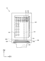
- FIG. 1 shows a top view of the display device 10.
- the display device 10 includes a substrate 100, a substrate 200, a display unit 101 having a plurality of pixels 103, a peripheral portion 104, a drive circuit 106 having a function as a source driver, and a drive having a function as a gate driver. It has a circuit 107, a flexible printed circuit board 108, and a terminal portion 109.
- the pixels 103 are provided in a matrix and include a display element (light emitting element 130 described later).
- the peripheral edge portion 104 is arranged outside the display unit 101 and is provided so as to surround the display unit 101.
- the pixel 103, the drive circuit 106, the drive circuit 107, and the flexible printed circuit board 108 are electrically connected to each other.
- Information (signals) from the external device is input to the drive circuit 106 and the drive circuit 107 via the flexible printed circuit board 108 and the terminal portion 109.
- FIG. 2 shows a circuit diagram of the pixel circuit 30 of the pixel 103 included in the display device 10.
- the circuit configuration of the pixel circuit 30 described below is an example, and is not limited to this.
- Each of the plurality of pixel circuits 30 includes at least a transistor 110, a transistor 111, a light emitting element 130, and a capacitance element 120.
- the transistor 110 and the transistor 111 can be collectively referred to as a semiconductor device.
- the transistor 110 is a transistor that is connected to the light emitting element 130 and controls the emission brightness of the light emitting element 130.
- the drain current of the transistor 110 is controlled by the gate-source voltage.
- the gate is connected to one of the source or drain of the transistor 111, one of the source or drain is connected to the drive power supply line 115, and the other of the source or drain is connected to the anode of the light emitting element 130.
- the transistor 111 is a transistor that controls the conduction state between the signal line 118 that sends a video signal from the drive circuit 106 and the gate of the transistor 110 by an on / off operation.
- the transistor 111 has a gate connected to a scanning line 113 that sends a scanning signal, a source connected to a signal line 118, and a drain connected to the gate of the transistor 110.
- the anode is connected to the drain of the transistor 110, and the cathode is connected to the reference power line 117.
- the capacitive element 120 is connected between the gate and drain of the transistor 110.
- the capacitive element 120 holds the gate-drain voltage of the transistor 110.
- the reference power line 117 is provided in common to the plurality of pixels 103. A constant potential is given to the reference power line.
- the video signal transmitted from the drive circuit 106 and the scanning signal transmitted from the drive circuit 107 are input to the respective pixels 103, so that the still image and the moving image are displayed on the display unit 101.
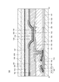
- FIG. 3 is a cross-sectional view between A1 and A2 of pixels 103 in the display device 10 shown in FIG.
- the pixel 103 includes a substrate 100, a transistor 110, a capacitive element 120, a light emitting element 130, an insulating layer 141, a flattening layer 150, ribs 157, a sealing layer 161 and an adhesive layer 190, and a substrate 200. .. Each configuration will be described in detail below.
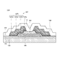
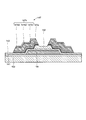
- FIG. 4 is an enlarged cross-sectional view of the transistor 110 of FIG.
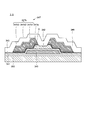
- the transistor 110 has a gate electrode 145, a gate insulating layer 143, an oxide semiconductor layer 142, and a source / drain electrode 147 and an insulating layer 149.
- the transistor 110 has a bottom gate top contact structure.
- the gate electrode 145 is provided on the insulating layer 141, that is, the insulating surface.
- the gate electrode 145 is provided with conductive materials such as aluminum (Al), titanium (Ti), chromium (Cr), cobalt (Co), nickel (Ni), zinc (Zn), molybdenum (Mo), and copper (Cu). ), Indium (In), tin (Sn), hafnium (Hf), tantalum (Ta), tungsten (W), platinum (Pt), bismuth (Bi) and the like. Further, an alloy of these metals may be used for the gate electrode 145.
- the gate electrode 145 is provided with conductive oxides such as ITO (indium tin oxide), IGO (indium tin oxide), IZO (indium zinc oxide), and GZO (zinc oxide to which gallium is added as a dopant). May be used. Moreover, these films may be laminated.
- the gate insulating layer 143 includes silicon nitride (SiN x ), silicon oxide (SiO x ), silicon nitride (SiO x Ny ), aluminum nitride (AlN x ), aluminum oxide (AlO x ), and aluminum nitride (AlO).
- x N y ) etc. are used (x, y are arbitrary integers).
- the gate insulating layer 143 may have a single-layer structure or a laminated structure of the above materials.
- the gate insulating layer 145 in contact with the oxide semiconductor layer 142 is preferably an insulating layer containing oxygen such as a silicon oxide film.
- the oxide semiconductor layer 142 is provided on the gate insulating layer 143.
- the oxide semiconductor layer 142 is arranged so as to overlap the gate electrode 145.
- the oxide semiconductor layer 142 can contain Group 13 elements such as indium and gallium.
- the oxide semiconductor layer 142 may contain a plurality of different Group 13 elements.
- the oxide semiconductor layer 142 may further contain a Group 12 element.
- IGZO a compound containing indium, gallium, and zinc is used for the oxide semiconductor layer 142.
- the oxide semiconductor layer 142 may contain other elements.
- the oxide semiconductor layer 142 may contain tin, which is a Group 14 element, titanium, zirconium, and the like, which are Group 4 elements.
- oxide semiconductor layer 142 InO x , ZnO x , SnO x , In—Ga—O, In—Zn—O, In—Al—O, In—Sn—O, In—Hf—O.
- the crystallinity of the oxide semiconductor layer 142 is not limited, and may be single crystal, polycrystalline, microcrystal, or amorphous.
- the oxide semiconductor layer 142 has few crystal defects such as oxygen deficiency. Further, the oxide semiconductor layer 142 preferably has a low hydrogen concentration.
- the source / drain electrode 147 includes a conductive layer 147a (also referred to as a first conductive layer) and a conductive layer 147b (also referred to as a second conductive layer).
- the conductive layer 147a is provided on the oxide semiconductor layer 142 and the gate insulating layer 143.
- the conductive layer 147a contains nitrogen together with the metallic material. Titanium nitride (TiN x ) is used for the conductive layer 147a in this example. By containing nitrogen, the conductive layer 147a has a function of diffusing oxygen from the oxide semiconductor layer 142 to a part of the conductive layer 147a and suppressing the diffusion of oxygen to the conductive layer 147b.
- the conductive layer 147a is not limited to titanium nitride, and tantalum nitride (TaN x ), molybdenum nitride (MoN x ), and tungsten nitride (WN x ) may be used (x is an arbitrary integer).
- the film thickness of the conductive layer 147a may be appropriately set, and is preferably 10 nm or more and 30 nm or less.
- the conductive layer 147b is provided on the conductive layer 147a.
- a metal material having a low resistance is used for the conductive layer 147b.
- the conductive layer 147b has aluminum (Al), titanium (Ti), chromium (Cr), cobalt (Co), nickel (Ni), zinc (Zn), molybdenum (Mo), copper (Cu), and indium (In).
- Tin (Sn), Hafnium (Hf), Tantal (Ta), Tungsten (W), Platinum (Pt), Bismuth (Bi) and the like are used. Alloys of these metals may be used for the conductive layer 147b. Further, these films may be laminated on the conductive layer 147b.
- the conductive layer 147b is laminated with the conductive layer 147b1, the conductive layer 147b2, and the conductive layer 147b3. Titanium is used for the conductive layer 147b1 and the conductive layer 147b3 in this example. Aluminum is used for the conductive layer 147b2 in this example.
- the film thickness of the conductive layer 147b may be appropriately set, and is preferably 50 nm or more and 1000 nm or less.
- FIG. 5 is an enlarged view of the oxide semiconductor layer 142 and the source / drain electrode 147 of the region A shown in FIG.
- a conductive layer 147c (also referred to as a third conductive layer) may be provided between the oxide semiconductor layer 142 and the conductive layer 147a of the source / drain electrodes 147.
- the conductive layer 147c contains oxygen diffused from the oxide semiconductor layer 142 together with the metal material of the conductive layer 147a.
- the content of oxygen contained in the conductive layer 147c is preferably 5 atomic% or more and 20 atomic% or less.
- the conductive layer 147c may further contain a part of the metal material contained in the oxide semiconductor layer 142.
- the thickness of the conductive layer 147c is preferably 2 nm or more and 10 nm or less. As a result, the conductive layer 147c can have conductivity.
- the insulating layer 149 is provided on the oxide semiconductor layer 142, the source / drain electrode 147, and the gate insulating layer 143.
- An insulating material containing oxygen is used for the insulating layer 149.
- silicon oxide (SiO x ) is used for the insulating layer 149 (x is an arbitrary integer).
- the insulating layer 149 is not limited to silicon oxide, and silicon oxide (SiO x N y ), aluminum oxide (AlO x ), aluminum nitride (AlO x N y ), or the like may be used (x, y is an arbitrary integer).
- the insulating layer 149 is preferably a film capable of releasing oxygen by heat treatment. Further, the insulating layer 149 preferably has a small defect level density.
- the source / drain electrode since the source / drain electrode has a conductive layer containing nitrogen on the oxide semiconductor layer 142 side, the diffusion of oxygen from the oxide semiconductor layer 142 is suppressed. Further, when the heat treatment is performed, oxygen diffuses from the oxide semiconductor layer to the source / drain electrode (specifically, the conductive layer 147a) to form a conductive region, and the entire source / drain electrode (specifically, the conductive layer 147a) is formed. Since oxidation as the conductive layer 147b) is suppressed, fluctuations in the characteristics of the transistor 110 can be reduced. Therefore, the reliability of the transistor 110 can be improved, and the reliability of the display performance in the display device can also be improved.
- a glass substrate or an organic resin substrate is used as the substrate 100.
- the organic resin substrate for example, polyimide is used.
- the organic resin substrate is not limited to polyimide, and polyethylene terephthalate, polyethylene naphthalate, triacetyl cellulose, cyclic olefin copolymer, cycloolefin polymer and the like may be used.
- the thickness of the substrate 100 and the substrate 200 can be appropriately set. In the case of an organic resin substrate, it is possible to realize a flexible sheet display.
- the insulating layer 141 has a function as a base film. Silicon oxide, silicon oxide, silicon nitride, or the like is used for the insulating layer 141.
- the insulating layer 141 may be a single layer or a laminated layer. By using the above material, it is possible to suppress the diffusion of impurities, typically alkali metals, water, hydrogen and the like from the substrate 100 into the oxide semiconductor layer 142.
- the flattening layer 150 is provided on the insulating layer 149.
- Polyimide, polyamide, acrylic, epoxy or the like is used for the flattening layer 150. These materials have a feature that a film can be formed by a solution coating method and a flattening effect is high. Further, the insulating layer 149 and the flattening layer 150 are provided with openings.
- the insulating layer 154 is used as a dielectric, and the conductive layer 153 and the pixel electrode 155 are used. Further, the conductive layer 151 provided in the same layer of the conductive layer 153 is connected to the source / drain electrode 147 and also to the pixel electrode 155.
- a pixel electrode 155, an organic EL layer 159, and a counter electrode 160 are used for the light emitting element 130.
- the light emitting element 130 has a so-called top emission type structure in which the light emitted by the organic EL layer 159 is radiated to the counter electrode 160 side.
- the organic EL layer 159 is provided on the pixel electrode 155 and has a light emitting material such as an organic electroluminescence material. Further, as the organic EL layer 159, a hole transport material and an electron transport material may be used together with the light emitting material. Further, the organic EL layer 159 of the present embodiment may be provided with a light emitting material for emitting light in a laminated manner. At this time, the display device 10 may display each color of RGB through a color filter.
- An organic resin material is used for the rib 157 in order to cover the peripheral region of the pixel electrode 155 and to form a smooth step at the end of the pixel electrode 155. Further, the rib 157 may use an organic resin material containing a black pigment in order to increase the contrast ratio of the displayed image.
- the sealing layer 161 is arranged on the light emitting element 130 and the rib 157.
- the sealing layer 161 includes an inorganic insulating layer 162, an organic insulating layer 163, and an inorganic insulating layer 164.
- An insulating film such as silicon nitride, silicon oxide, or aluminum oxide is used for the inorganic insulating layer 162 and the inorganic insulating layer 164.
- the film thickness of the inorganic insulating layer 162 and the inorganic insulating layer 164 is preferably 30 nm or more and 1 ⁇ m or less.
- the film thickness of the organic insulating layer 163 is preferably 1 ⁇ m or more and 20 ⁇ m or less, preferably 3 ⁇ m or more and 10 ⁇ m or less.
- the organic insulating layer 163 By having the organic insulating layer 163 between the inorganic insulating layer 162 and the inorganic insulating layer 164, the surface of the organic insulating layer 163 is flattened even when foreign matter is mixed in when forming the sealing layer 161. To. Therefore, the coverage of the inorganic insulating layer 164 is increased. Therefore, the moisture blocking performance can be stably maintained.
- the substrate 200 may be provided on the inorganic insulating layer 164 via the adhesive layer 190.
- the adhesive layer 190 for example, an acrylic, rubber, silicone, urethane, or other adhesive material can be used.
- a touch panel may be provided on the substrate 200.
- the substrate 200 may have optical performance such as a polarizer.
- the adhesive layer 190 may contain a hygroscopic substance such as calcium or zeolite. Since the adhesive layer 190 contains a hygroscopic substance, it is possible to delay the arrival of the moisture in the light emitting element 130 even when the moisture invades the inside of the display device 10.
- a glass substrate, a quartz substrate, or a flexible substrate polyimide, polyethylene terephthalate, polyethylene naphthalate, triacetyl cellulose, cyclic olefin copolymer, cycloolefin polymer, or other flexible resin substrate
- a glass substrate polyimide, polyethylene terephthalate, polyethylene naphthalate, triacetyl cellulose, cyclic olefin copolymer, cycloolefin polymer, or other flexible resin substrate
- the adhesive layer 190 may be provided with a spacer in order to secure a gap between the substrate 100 and the substrate 200.
- a spacer may be mixed with the adhesive layer 190, or may be formed on the substrate 100 with a resin or the like.
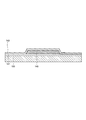
- a gate electrode 145 is formed on the insulating layer 141.
- a conductive film is formed on the insulating layer 141 provided on the substrate 100, and then processed into a desired shape by using a patterning method and an etching method to form a gate electrode 145.
- the conductive film is formed by a sputtering method in a single-layer structure or a laminated structure using the above-mentioned materials.
- the film thickness of the gate electrode 145 is preferably 100 nm or more and 500 nm or less. In this example, an alloy film of molybdenum and tungsten is used as the gate electrode 145.
- a gate insulating layer 143 is formed on the gate electrode 145 and the insulating layer 141.
- the gate insulating layer 143 is formed by a sputtering method, a thermal CVD method, or a plasma CVD method in a single-layer structure or a laminated structure using the above-mentioned materials.
- the formation temperature of the gate insulating layer 143 is preferably 325 ° C. or higher and 450 ° C. or lower, preferably 350 ° C. or higher and 400 ° C. or lower.
- the film thickness of the gate insulating layer 143 is preferably 50 nm or more and 500 nm or less.
- a material capable of releasing oxygen by heat treatment for the gate insulating layer 143.
- silicon oxide is preferably used as the gate insulating layer 143.
- the oxide semiconductor layer 142 is formed on the gate insulating layer 143.
- the oxide semiconductor layer 142 is formed by forming an oxide semiconductor film on the gate insulating layer 143 and then processing it into a desired shape by using a patterning method and an etching method.
- the oxide semiconductor film is preferably formed with a film thickness of 30 nm or more and 100 nm or less, for example, by using a sputtering method and setting the film formation temperature to 250 ° C. or more and 450 ° C. or less.
- the power source applied to the oxide semiconductor target may be a direct current (DC) or an alternating current power source (AC), and is determined by the shape and composition of the oxide semiconductor target. be able to.
- oxygen gas when forming the oxide semiconductor film, oxygen gas, a mixed gas of oxygen and a rare gas, or a rare gas may be used.
- the sputtering gas for forming the oxide semiconductor film in this example, it is preferably performed in a mixed gas atmosphere of oxygen and a rare gas, and the oxygen gas flow rate ratio to the rare gas is more preferably 5% or more. It is preferable to set the oxygen gas flow rate ratio to 5% or more because oxygen is easily added to the oxide semiconductor film.
- the heat treatment may be performed after the oxide semiconductor layer 142 is formed.
- the heat treatment may be performed before processing the oxide semiconductor film (before patterning treatment) or after processing (after etching). Since the volume of the oxide semiconductor layer 142 may become smaller (shrink) due to the heat treatment, it is preferable to perform the heat treatment before processing. Further, by heat-treating the oxide semiconductor layer 142, it is possible to improve the film quality such as reducing the hydrogen concentration and improving the density of the oxide semiconductor layer 142.
- the heat treatment performed on the oxide semiconductor layer 142 can be performed at atmospheric pressure or low pressure (vacuum) in the presence of nitrogen, dry air, or the atmosphere.
- the heat treatment is carried out at 250 ° C. or higher and 500 ° C. or lower, preferably 350 ° C. or higher and 450 ° C. or lower.
- the heating time is preferably, for example, 15 minutes or more and 1 hour or less.
- oxygen is introduced into the oxygen deficiency of the oxide semiconductor layer 142 or the oxygen is dislocated, so that the oxide semiconductor layer 142 having few crystal defects and high crystallinity can be obtained.
- the hydrogen concentration of the oxide semiconductor layer 142 can be reduced by the heat treatment. As a result, it is possible to manufacture a transistor having a low defect level density in the oxide semiconductor layer 142 and a small characteristic variation.
- a source / drain electrode 147 is formed on the oxide semiconductor layer 142.
- a conductive film to be a conductive layer 147a is formed on the oxide semiconductor layer 142.
- the conductive film to be the conductive layer 147a is formed by a sputtering method using the above-mentioned materials.
- the conductive film is not limited to the sputtering method, and may be formed by a CVD method or a printing method.
- the film thickness of the conductive layer 147a is preferably 10 nm or more and 50 nm or less. In this example, titanium nitride formed by the sputtering method is used as the conductive layer 147a.
- a conductive film to be the conductive layer 147b is formed on the conductive layer 147a.
- the conductive film to be the conductive layer 147b is formed by a single layer structure or a laminated structure by a sputtering method using the above-mentioned material, but may be formed by other methods.
- the film thickness of the conductive layer 147b is preferably 50 nm or more and 1000 nm or less.
- the conductive layer 147b1, the conductive layer 147b2, and the conductive layer 147b3 are continuously formed as the conductive layer 147b. More specifically, a titanium film is formed as the conductive layer 147b1 by a sputtering method.
- An aluminum film is formed as the conductive layer 147b2 by a sputtering method.
- a titanium film is formed as the conductive layer 147b3 by a sputtering method.
- the conductive layer 147a and the conductive layer 147b are collectively processed by a patterning method and an etching method, so that the source / drain electrode 147 has a desired shape.
- the conductive layer 147a and the conductive layer 147b may be processed separately instead of being processed all at once.
- an insulating layer 149 is formed on the oxide semiconductor layer 142 and the source / drain electrode 147.
- the insulating layer 149 is formed in a single layer structure or a laminated structure by using the above-mentioned materials by a plasma CVD method, a thermal CVD method, or a sputtering method.
- the formation temperature of the insulating layer 149 is preferably 325 ° C or higher and 450 ° C or lower, preferably 350 ° C or higher and 400 ° C or lower.
- the film thickness of the gate insulating layer 143 is preferably 100 nm or more and 500 nm or less.
- a material capable of releasing oxygen by heat treatment for the insulating layer 149, for example, a silicon oxide film is preferably used.
- heat treatment is performed.
- the heat treatment can be performed at atmospheric pressure or low pressure (vacuum) in the presence of nitrogen, dry air, or air.
- the heat treatment is preferably performed at 325 ° C. or higher and 450 ° C. or lower, preferably 350 ° C. or higher and 400 ° C. or lower.
- the heating time is preferably, for example, 15 minutes or more and 12 hours or less, preferably 30 minutes or more and 2 hours or less.
- oxygen deficiency contained in the oxide semiconductor layer 142 can be reduced, and an oxide semiconductor layer 142 having few crystal defects and high crystallinity can be obtained.
- the hydrogen concentration of the oxide semiconductor layer 142 can be reduced by the heat treatment. Further, the heat treatment reduces the defect level density contained in the gate insulating layer 143 and the insulating layer 149. As a result, the defect level density of the entire transistor 110 is reduced.
- the oxide semiconductor layer 142 has a conductive region (n + region).
- a part of the source / drain electrode 147 may be oxidized by the diffused oxygen.
- titanium when used as the source / drain electrode, it reacts with the oxide semiconductor layer 142 to form a good n + region, but easily reacts with oxygen. For this reason, the reaction with oxygen continues to proceed due to the driving stress (temperature, voltage, light, etc.).
- the driving stress temperature, voltage, light, etc.
- the source / drain electrode 147 includes a conductive layer 147a having nitrogen at a portion in contact with the oxide semiconductor layer 142.
- the conductive layer 147a As a result, when the heat treatment is performed after the insulating layer 149 is formed, oxygen diffuses from the oxide semiconductor layer 142 to the source / drain electrode 147 side (specifically, the conductive layer 147a).
- the conductive region (n + region) is effectively formed, and oxidation of the entire source / drain electrode (specifically, the conductive layer 147b) is suppressed.
- the conductive layer 147c (also referred to as the third conductive layer) may be formed between the oxide semiconductor layer 142 and the conductive layer 147a of the source / drain electrodes by the heat treatment.
- the conductive layer 147c contains the metallic material and oxygen contained in the conductive layer 147a. Further, the conductive layer 147c may further contain a part of the metal material contained in the oxide semiconductor layer 142. In this example, the conductive layer 147c contains titanium and oxygen, and may also contain indium, gallium, and zinc, respectively.
- the film thickness of the conductive layer 147c is preferably 2 nm or more and 10 nm.
- the transistor 110 having the above configuration good ohmic contact can be formed between the oxide semiconductor layer 142 and the source / drain electrode 147. Further, the transistor 110 suppresses oxidation of the entire source / drain electrode due to stress (temperature, voltage, light, etc.) when driving the display device. Further, by forming the gate insulating layer and the oxide insulating layer at a high temperature and performing heat treatment, the defect level density in the gate insulating layer and the oxide insulating layer is reduced. Therefore, the transistor 110 of the present embodiment can have high reliability because fluctuations in characteristics such as drain current and threshold voltage can be suppressed. Therefore, the display device of the present embodiment can have high display reliability by including the transistor 110.
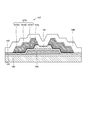
- FIG. 11 is a cross-sectional view of the transistor 110A according to the present embodiment.
- the transistor 110A is provided on the insulating layer 141 and has an insulating layer 146 in addition to the gate electrode 145, the gate insulating layer 143, the oxide semiconductor layer 142, the source / drain electrode 147, and the insulating layer 149.
- the insulating layer 146 is provided on the gate insulating layer 143 and the oxide semiconductor layer 142.
- the same material as that of the insulating layer 149 is used.
- a silicon oxide film is used for the insulating layer 146.
- the transistor 110A has a structure that protects the back channel side of the oxide semiconductor layer 142 by having the insulating layer 146 on the oxide semiconductor layer 142.
- an insulating layer 146 is formed on the gate insulating layer 143. It is desirable that the insulating layer 146 is formed by the same method as that of the insulating layer 149.
- the formation temperature of the insulating layer 146 is preferably 325 ° C. or higher and 450 ° C., preferably 350 ° C. or higher and 400 ° C. or lower.
- heat treatment may be appropriately performed. It is desirable that the heat treatment is carried out at 325 ° C. or higher and 450 ° C. or lower, preferably 350 ° C. or higher and 400 ° C. or lower, and 15 minutes or longer and 12 hours or shorter, preferably 30 minutes or longer and 2 hours or shorter.
- the pore 146a is formed on the oxide semiconductor layer 142 by a patterning method and a dry etching method.
- a source / drain electrode 147 is formed on the insulating layer 146.
- the steps after the formation of the source / drain electrode 147 are the same as those in the first embodiment.
- good ohmic contact can be formed between the oxide semiconductor layer 142 and the source / drain electrode 147 while protecting the oxide semiconductor layer 142, and when the display device is driven. Oxidation of the entire source / drain electrode 147 (specifically, the conductive layer 147b) due to stress (temperature, voltage, light, etc.) is suppressed. Therefore, a transistor having high reliability can be provided, and a display device having high reliability can be provided.
- a transistor different from that of the first embodiment will be described.
- the transistor 110B having a top gate structure will be described with reference to FIG.
- the same structure, material, and manufacturing method as the transistors according to the first embodiment and the second embodiment will not be described.
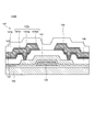
- FIG. 14 is a cross-sectional view of the transistor 110B according to the present embodiment.
- the transistor 110B is provided on the insulating layer 141 and has an oxide semiconductor layer 142B, a gate insulating layer 143B, a gate electrode 145B, an insulating layer 146B, a source / drain electrode 147B, and an insulating layer 149B. ..
- the oxide semiconductor layer 142B is arranged on the insulating layer 141.
- the gate insulating layer 143B is arranged on the insulating layer 141 and the oxide semiconductor layer 142B.
- the gate electrode 145B is arranged on the gate insulating layer 143B.
- the insulating layer 146B is arranged on the gate insulating layer 143B and the gate electrode 145B.
- the source / drain electrode 147B is arranged on the insulating layer 146B and in contact with the oxide semiconductor layer 142B.
- the insulating layer 149B is arranged on the insulating layer 146B and the source / drain electrode 147B.
- the transistor 110B is provided with a gate electrode 145B on the oxide semiconductor layer 142B. Further, the transistor 110B can reduce the transistor size as compared with the transistor 110 by controlling the size of the gate electrode 145B. Further, the oxide semiconductor layer 142B is entirely covered with the insulating layer 146B, and defects such as oxygen deficiency in the oxide semiconductor layer 142B are reduced by forming the insulating layer 146B and performing heat treatment. be able to. Therefore, good ohmic contact can be formed between the oxide semiconductor layer 142 and the source / drain electrode 147 while protecting the oxide semiconductor layer.
- the oxidation of the entire source / drain electrode 147 (specifically, the conductive layer 147b) due to stress (temperature, voltage, light, etc.) when driving the display device is suppressed. Therefore, by using this embodiment, it is possible to provide a transistor having high reliability and to provide a display device having high reliability.
- a display device different from the first embodiment will be described with reference to FIG. Specifically, a display device using a liquid crystal element in the pixels 103 shown in FIGS. 1 and 3 will be described.
- the example of using the transistor 110 described in the first embodiment will be described, but the transistor 110A of the second embodiment and the transistor 110B of the third embodiment may be used.
- FIG. 15 is a cross-sectional view of pixel 103C.
- the pixel 103C includes a liquid crystal element 131, a color filter layer 195, and a light-shielding layer 197 in addition to the substrate 100, the insulating layer 141, the transistor 110, the flattening layer 150, and the substrate 200.
- the pixel electrode 171 is provided on the flattening layer 150.
- a transparent conductive material is used for the pixel electrode 171.
- ITO indium tin oxide
- ZnO zinc oxide
- IZO indium zinc oxide
- the pixel electrode 171 is connected to the source / drain electrode 147 via an opening.
- the pixel electrode 171 is separated for each pixel and is provided in a comb-teeth shape in a plan view.
- the insulating layer 172 is provided on the pixel electrode 171.
- a silicon oxide film or a silicon nitride film is used for the insulating layer 172.
- the common electrode 173 is provided on the insulating layer 172.
- the same material as the pixel electrode 171 can be used for the common electrode 173.
- the common electrode 173 is provided across each pixel in a plan view. In this example, the common electrode 173 is arranged on the upper side of the pixel electrode 171 but is not limited to this and may be arranged on the lower side of the pixel electrode 171. Further, although the common electrode 173 is also provided in a comb-teeth shape in the cross-sectional view of the present embodiment, it may be provided continuously.
- the light-shielding layer 197 is provided on the substrate 200 side.
- the light-shielding layer 197 has a function of light-shielding.
- an inorganic film such as a black chromium film, carbon black, or a composite oxide containing a solid solution of a plurality of inorganic oxides can be used.
- the color filter layer 195 is provided at the opening of the light shielding layer 196.
- the color filter layer 195 has a function of transmitting light in a specific wavelength band with respect to the light transmitted and emitted from the liquid crystal element 131. For example, light in the red, green, or blue wavelength band can be transmitted.
- the flattening layer 191 is provided on the color filter layer 195 and the light shielding layer 197.
- the same material as the flattening layer 150 is used for the flattening layer 191.
- a liquid crystal layer 175 is provided between the common electrode 173 and the flattening layer 191.
- An FFS (Fringe Field Switching) type liquid crystal element is used for the liquid crystal element 131 of the present embodiment composed of the pixel electrode 171 and the common electrode 173 and the liquid crystal layer 175.
- various liquid crystal elements such as TN type and VA type may be used.
- the transistor 110 by using the transistor 110, it is possible to suppress fluctuations in transistor characteristics against long-term driving stress. Therefore, it is possible to provide a liquid crystal display device having high reliability.
- FIG. 16 is a cross-sectional view of the transistor 310 produced in this embodiment.
- the transistor 310 includes a gate electrode 345, a gate insulating layer 343, an oxide semiconductor layer 342, and a source / drain electrode 347 on a substrate 300 and an insulating layer 341 which are 6th generation glass substrates (1,500 mm ⁇ 1,850 mm). And has an insulating layer 349.
- the transistor 310 has the same configuration as the transistor 110 of the first embodiment of the present invention. The method for manufacturing the transistor 310 is shown below.
- an insulating layer 341 of silicon oxide was formed on the substrate, and a gate electrode 345 was formed on the insulating layer 341.
- a 200 nm molybdenum and tungsten alloy film (MoW) was formed by a DC sputtering method and processed by a patterning method and a dry etching method.
- a gate insulating layer 343 was formed on the gate electrode 345.
- a laminated film of a silicon nitride film having a film thickness of 150 nm and a silicon oxide film having a film thickness of 100 nm was formed at 350 ° C. by a plasma CVD method.
- an oxide semiconductor layer 342 was formed on the gate insulating layer 343 so as to overlap the gate electrode 345.
- an IGZO film having a film thickness of 75 nm was formed at 100 ° C. by an AC sputtering method, and processed by a patterning method and a dry etching method.
- a source / drain electrode 347 was formed on the oxide semiconductor layer 342.
- the source / drain electrode 347 titanium nitride (TiN) having a film thickness of 20 nm, titanium (Ti) having a film thickness of 50 nm, aluminum (Al) having a film thickness of 200 nm, and titanium (Ti) having a film thickness of 50 nm are laminated by a sputtering method. The film was filmed and processed in a batch by the patterning method and the dry etching method.
- an insulating layer 349 was formed on the source / drain electrode 347.
- a silicon oxide film having a film thickness of 300 nm was formed at 350 ° C. by a plasma CVD method.
- FIG. 17 shows a transmission electron microscope-energy dispersive X-ray analysis (TEM-EDX) of the interface region A between the oxide semiconductor layer 342 of the transistor 310 and the source / drain electrode layer after forming the insulating layer 349 and heat-treated. )
- TEM-EDX transmission electron microscope-energy dispersive X-ray analysis
- the transistor 310 was manufactured on a 6th generation glass substrate (1,500 mm ⁇ 1,850 mm).
- the manufacturing conditions for the transistor 310 are the same as in the first embodiment.
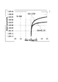
- the Id-Vg characteristics of 84 transistors made on a 6th generation glass substrate were evaluated.
- the Id-Vg characteristic of the transistor 310 was measured by applying a voltage (Vg) applied to the gate electrode 345 of the transistor 310 from ⁇ 15 V to + 15 V in 0.1 V steps.
- the voltage (Vs) applied to the source electrode of the source / drain electrodes 347 was set to 0V
- the voltage (Vd) applied to the drain electrode was set to 0.1V and 10V.
- the measurement of Id-Vg characteristics was performed at room temperature.
- FIG. 18 shows the results of evaluating the Id-Vg characteristics of 84 transistors manufactured on a 6th generation glass substrate.
- Table 1 summarizes the field effect mobility ( ⁇ FE), the threshold voltage (Vth), and the subthreshold value (SS) as the results of evaluating the Id-Vg characteristics of the 84 transistors.
- the field effect mobility ( ⁇ FE) refers to the channel mobility obtained from the change in the drain current with respect to the gate voltage when the drain voltage is constant in the linear region of the metal oxide semiconductor field effect transistor (MOSFET) operation.
- the threshold voltage (Vth) refers to the gate voltage required to pass the drain current in the MOSFET.
- the subthreshold value (SS) refers to the rate at which the MOSFET current (drain current) increases with respect to the voltage (gate voltage).
- the average value, 3 ⁇ , maximum value (Mix) and minimum value (Min) of the field effect mobility ( ⁇ FE (cm 2 / V ⁇ s)) of the 84 transistors 310 are They were 12.36, 1.88, 13.66, and 11.30, respectively.
- the average value (Average), 3 ⁇ , maximum value (Mix) and minimum value (Min) of the threshold voltage (Vth (V)) were 0.65, 0.17, 0.73, 0.53, respectively.
- the average value (Average), 3 ⁇ , maximum value (Mix) and minimum value (Min) of the subthreshold value (SS (V / decode)) are 0.10, 0.05, 0.12, 0, respectively. It was .07. Therefore, it was found that the transistor 310 of this embodiment showed stable characteristics without any variation in characteristics.
- a gate bias-heat stress test (hereinafter referred to as a GBT test) was performed on the manufactured transistor 310.
- the gate voltage (Vg) was -40V
- the drain voltage (Vd) and the source voltage (Vs) were 0V
- the stress temperature was 125 ° C.
- the measurement environment was dark.
- the Id-Vg characteristics of the transistor 310 were measured at stress times of 0 sec, 100 sec, 500 sec, and 1000 sec.
- FIG. 19 shows the reliability evaluation result of the Id-Vg characteristic. As shown in FIG. 19, no change in the characteristics of the transistor 310 of this embodiment was observed even when the stress time passed 1000 sec.
- the following transistor 410 was manufactured and the reliability of the Id-Vg characteristics was evaluated.
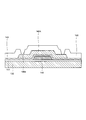
- FIG. 20 is a cross-sectional view of the transistor 410 of the comparative example.
- the transistor 410 of the comparative example has a gate electrode 445, a gate insulating layer 443, an oxide semiconductor layer 442, a source / drain electrode 447, and an insulating layer 449 on a substrate 400 and an insulating layer 441.
- the transistor 410 is the same as the transistor 310 except that the source / drain electrode 447 does not have the conductive layer 347a containing nitrogen in the portion in contact with the oxide semiconductor layer 342 like the transistor 310.
- the film formation temperature of the gate insulating layer 443 and the insulating layer 449 and the heat treatment temperature after the formation of the insulating layer 449 are set to 300 ° C. or lower, and oxidation occurs between the oxide semiconductor layer 442 and the source / drain electrode 447.
- An object specifically, titanium oxide was prevented from being formed.
- FIG. 21 shows the results of the Id-Vg characteristics of the transistor 310 of the comparative example. As shown in FIG. 21, it was found that in the transistor 410 of the comparative example, the Id-Vg characteristics fluctuated as the stress application time increased.
- the present invention is not limited thereto.
- An oxide semiconductor layer 142 may be provided on the source / drain electrode 147.
- the conductive layer 147a may be provided above the source / drain electrode 147.
- the gate electrode may be provided on the upper side of the oxide semiconductor layer 142, or the oxide semiconductor 142 may be sandwiched between two gate electrodes provided on the upper side and the lower side thereof.
Landscapes
- Physics & Mathematics (AREA)
- Engineering & Computer Science (AREA)
- Nonlinear Science (AREA)
- Microelectronics & Electronic Packaging (AREA)
- Crystallography & Structural Chemistry (AREA)
- Chemical & Material Sciences (AREA)
- Mathematical Physics (AREA)
- General Physics & Mathematics (AREA)
- Optics & Photonics (AREA)
- Manufacturing & Machinery (AREA)
- Thin Film Transistor (AREA)
- Devices For Indicating Variable Information By Combining Individual Elements (AREA)
- Electroluminescent Light Sources (AREA)
- Electrodes Of Semiconductors (AREA)
- Semiconductor Integrated Circuits (AREA)
Abstract
Description
(1-1.表示装置の構成)
図1は、表示装置10の上面図を示す。図1において、表示装置10は、基板100、基板200、複数の画素103を有する表示部101と、周縁部104、ソースドライバとしての機能を有する駆動回路106と、ゲートドライバとしての機能を有する駆動回路107、フレキシブルプリント基板108、および端子部109を有する。
次に、表示装置10の画素103の各構成について、図面を用いて説明する。
図4は、図3のトランジスタ110を拡大した断面図である。トランジスタ110は、ゲート電極145、ゲート絶縁層143、酸化物半導体層142、およびソース・ドレイン電極147、絶縁層149を有する。本実施形態では、トランジスタ110は、ボトムゲート・トップコンタクト構造を有する。
図3に戻って、表示装置10のその他の各構成について以下に説明する。
次に、表示装置10のうちトランジスタ110の製造方法について、図6乃至図10を参照して説明する。
本実施形態では、第1実施形態と形態が異なるトランジスタについて説明する。具体的には、チャネル保護型トランジスタの構造について図面を参照して説明する。なお、第1実施形態に係る半導体装置と同様の構造、材料、および製造方法については、適宜説明を省略する。
図11は、本実施形態に係るトランジスタ110Aの断面図である。トランジスタ110Aは、絶縁層141上に設けられ、ゲート電極145、ゲート絶縁層143、酸化物半導体層142、ソース・ドレイン電極147、および絶縁層149に加えて絶縁層146を有する。
次に、本実施形態に係るトランジスタ110Aの製造方法について、図12及び図13を参照して説明する。まず、第1実施形態で説明したように、ゲート絶縁層143上に、酸化物半導体層142を形成する。
本実施形態では、第1実施形態と形態が異なるトランジスタについて説明する。具体的には、トップゲート構造を有するトランジスタ110Bについて図14を参照して説明する。なお、第1実施形態および第2実施形態に係るトランジスタと同様の構造、材料、および製造方法については、説明を省略する。
図14は、本実施形態に係るトランジスタ110Bの断面図である。図14に示すように、トランジスタ110Bは、絶縁層141上に設けられ、酸化物半導体層142B、ゲート絶縁層143B、ゲート電極145B、絶縁層146B、ソース・ドレイン電極147B、および絶縁層149Bを有する。
本実施形態では、第1実施形態と異なる表示装置について、図15を参照して説明する。具体的には、図1および図3に示す画素103において、液晶素子を用いる表示装置について説明する。なお、本実施形態では、第1実施形態で説明したトランジスタ110を用いる例について説明するが、第2実施形態のトランジスタ110A及び第3実施形態のトランジスタ110Bを用いてもよい。
図15は、画素103Cの断面図である。画素103Cは、基板100、絶縁層141、トランジスタ110、平坦化層150、および基板200に加えて、液晶素子131、カラーフィルタ層195および遮光層197を含む。

図20は、比較例のトランジスタ410の断面図である。比較例のトランジスタ410は基板400、絶縁層441上にゲート電極445、ゲート絶縁層443、酸化物半導体層442、ソース・ドレイン電極447、および絶縁層449を有する。トランジスタ410は、ソース・ドレイン電極447が、トランジスタ310のように窒素を含む導電層347aを酸化物半導体層342と接する部分に有していない以外はトランジスタ310と同様である。また、トランジスタ410は、ゲート絶縁層443および絶縁層449の成膜温度および絶縁層449形成後の加熱処理温度は300℃以下とし、酸化物半導体層442とソース・ドレイン電極447との間で酸化物(具体的には、酸化チタン)が形成されないようにした。
本発明の第1~第3実施形態では、酸化物半導体層142上にソース・ドレイン電極147が設けられる例を示したが、これに限定されない。ソース・ドレイン電極147上に酸化物半導体層142が設けられてもよい。この場合、ソース・ドレイン電極147の上側に導電層147aが設けられてもよい。また、ゲート電極が酸化物半導体層142の上側に設けられてもよいし、酸化物半導体142がその上側と下側に設けられた2つのゲート電極により挟まれてもよい。
Claims (10)
- 絶縁表面上のゲート電極と、
前記ゲート電極上のゲート絶縁層と、
前記ゲート絶縁層上に配置され、前記ゲート電極と重畳する酸化物半導体層と、
前記酸化物半導体層および前記ゲート絶縁層上の窒素を含む第1導電層および前記第1導電層上の第2導電層を含むソース・ドレイン電極と、
前記酸化物半導体層および前記ソース・ドレイン電極上の酸素を含む絶縁層と、
を含む、トランジスタと、
前記トランジスタ上の表示素子と、
を含む表示装置。 - 前記第1導電層と前記酸化物半導体層との間に酸素を含む第3導電層を含む、
請求項1に記載の表示装置。 - 前記第3導電層は、前記酸化物半導体層の一部の金属材料を含む、
請求項2に記載の表示装置。 - 前記第3導電層の厚さは、2nm以上10nm以下である
請求項2に記載の表示装置。 - 前記第3導電層中の酸素の含有量は、10atmic%以上である、
請求項2乃至4のいずれか一項に記載の表示装置。 - 絶縁表面上にゲート電極を形成し、
前記ゲート電極上にゲート絶縁層を形成し、
前記ゲート絶縁層上に、前記ゲート電極と重畳する領域を含む酸化物半導体層を形成し、
前記酸化物半導体層および前記ゲート絶縁層上に、窒素を含む第1導電層、および前記第1導電層上の第2導電層を含むソース・ドレイン電極を形成し、
前記ソース・ドレイン電極上に絶縁層を形成し、
加熱処理を行うことによりトランジスタを形成し、
前記トランジスタ上に表示素子を形成する、
表示装置の製造方法。 - 前記ゲート絶縁層の形成温度と前記加熱処理の温度は、325℃以上450℃以下である、
請求項6に記載の表示装置の製造方法。 - 前記ゲート絶縁層の形成温度と前記加熱処理の温度は、350℃以上400℃以下である、
請求項6に記載の表示装置の製造方法。 - 前記加熱処理によって、前記酸化物半導体層と前記第1導電層との間に酸素を含む第3導電層が形成される、
請求項7または8に記載の表示装置の製造方法。 - 前記第3導電層は、前記酸化物半導体層に含まれる一部の金属材料を含む、
請求項9に記載の表示装置の製造方法。
Priority Applications (5)
| Application Number | Priority Date | Filing Date | Title |
|---|---|---|---|
| KR1020217032976A KR102650842B1 (ko) | 2019-03-28 | 2020-03-13 | 표시 장치 및 표시 장치의 제조 방법 |
| CN202080019549.9A CN113544859A (zh) | 2019-03-28 | 2020-03-13 | 显示装置和显示装置的制造方法 |
| DE112020000878.9T DE112020000878B4 (de) | 2019-03-28 | 2020-03-13 | Anzeigevorrichtung |
| US17/447,740 US11927859B2 (en) | 2019-03-28 | 2021-09-15 | Display device and method for manufacturing display device |
| US18/594,462 US12298640B2 (en) | 2019-03-28 | 2024-03-04 | Display device and method for manufacturing display device |
Applications Claiming Priority (2)
| Application Number | Priority Date | Filing Date | Title |
|---|---|---|---|
| JP2019-063815 | 2019-03-28 | ||
| JP2019063815A JP2020167188A (ja) | 2019-03-28 | 2019-03-28 | 表示装置および表示装置の製造方法 |
Related Child Applications (1)
| Application Number | Title | Priority Date | Filing Date |
|---|---|---|---|
| US17/447,740 Continuation US11927859B2 (en) | 2019-03-28 | 2021-09-15 | Display device and method for manufacturing display device |
Publications (1)
| Publication Number | Publication Date |
|---|---|
| WO2020195972A1 true WO2020195972A1 (ja) | 2020-10-01 |
Family
ID=72611439
Family Applications (1)
| Application Number | Title | Priority Date | Filing Date |
|---|---|---|---|
| PCT/JP2020/011184 Ceased WO2020195972A1 (ja) | 2019-03-28 | 2020-03-13 | 表示装置および表示装置の製造方法 |
Country Status (6)
| Country | Link |
|---|---|
| US (2) | US11927859B2 (ja) |
| JP (1) | JP2020167188A (ja) |
| KR (1) | KR102650842B1 (ja) |
| CN (1) | CN113544859A (ja) |
| DE (1) | DE112020000878B4 (ja) |
| WO (1) | WO2020195972A1 (ja) |
Families Citing this family (2)
| Publication number | Priority date | Publication date | Assignee | Title |
|---|---|---|---|---|
| JP7516210B2 (ja) | 2020-10-29 | 2024-07-16 | 株式会社ジャパンディスプレイ | 半導体装置の製造方法 |
| CN114284362B (zh) * | 2021-12-27 | 2025-07-29 | 广东省科学院半导体研究所 | 薄膜晶体管、薄膜晶体管的制备方法和显示器件 |
Citations (4)
| Publication number | Priority date | Publication date | Assignee | Title |
|---|---|---|---|---|
| JP2007284342A (ja) * | 2006-04-18 | 2007-11-01 | Samsung Electronics Co Ltd | ZnO半導体薄膜及びZnO薄膜トランジスタの製造方法、並びにその方法を適用したZnO薄膜トランジスタ |
| JP2014082388A (ja) * | 2012-10-17 | 2014-05-08 | Semiconductor Energy Lab Co Ltd | 半導体装置 |
| JP2014099602A (ja) * | 2012-10-17 | 2014-05-29 | Semiconductor Energy Lab Co Ltd | 半導体装置 |
| JP2014112659A (ja) * | 2012-10-24 | 2014-06-19 | Semiconductor Energy Lab Co Ltd | 半導体装置 |
Family Cites Families (27)
| Publication number | Priority date | Publication date | Assignee | Title |
|---|---|---|---|---|
| JPH07104505B2 (ja) | 1987-09-04 | 1995-11-13 | 凸版印刷株式会社 | 液晶表示装置のマトリックス駆動方法 |
| US4799077A (en) | 1987-11-23 | 1989-01-17 | Polaroid Corporation | Common drive for shutter blades and objective lens assembly |
| JP5126729B2 (ja) | 2004-11-10 | 2013-01-23 | キヤノン株式会社 | 画像表示装置 |
| US7791072B2 (en) | 2004-11-10 | 2010-09-07 | Canon Kabushiki Kaisha | Display |
| JP2008091599A (ja) * | 2006-10-02 | 2008-04-17 | Sony Corp | 薄膜トランジスタおよびその製造方法ならびに表示装置 |
| TWI352431B (en) * | 2008-01-08 | 2011-11-11 | Au Optronics Corp | Active matrix array structure and manufacturing me |
| US8187919B2 (en) * | 2008-10-08 | 2012-05-29 | Lg Display Co. Ltd. | Oxide thin film transistor and method of fabricating the same |
| KR101213708B1 (ko) * | 2009-06-03 | 2012-12-18 | 엘지디스플레이 주식회사 | 어레이 기판 및 이의 제조방법 |
| US8906739B2 (en) * | 2010-04-06 | 2014-12-09 | Sharp Kabushiki Kaisha | Thin film transistor substrate and method for manufacturing same |
| KR101706081B1 (ko) * | 2010-04-06 | 2017-02-15 | 삼성디스플레이 주식회사 | 박막 트랜지스터, 그 제조 방법 및 이를 포함하는 액정 표시 장치 |
| JP5133469B2 (ja) * | 2010-06-08 | 2013-01-30 | シャープ株式会社 | 薄膜トランジスタ基板及びそれを備えた液晶表示装置並びに薄膜トランジスタ基板の製造方法 |
| KR101782081B1 (ko) * | 2010-08-30 | 2017-09-26 | 엘지이노텍 주식회사 | 발광 소자 |
| KR101895421B1 (ko) * | 2011-02-24 | 2018-09-07 | 삼성디스플레이 주식회사 | 배선, 박막 트랜지스터, 및 박막 트랜지스터 표시판과 이들을 제조하는 방법들 |
| CN102655165B (zh) * | 2011-03-28 | 2015-04-29 | 京东方科技集团股份有限公司 | 一种非晶氧化物薄膜晶体管及其制作方法、显示面板 |
| DE112012004061B4 (de) | 2011-09-29 | 2024-06-20 | Semiconductor Energy Laboratory Co., Ltd. | Halbleitervorrichtung |
| KR101926513B1 (ko) * | 2011-11-09 | 2018-12-11 | 엘지디스플레이 주식회사 | 산화물 박막트랜지스터를 포함하는 액정표시장치 및 액정표시장치 제조방법 |
| TWI458150B (zh) * | 2012-01-11 | 2014-10-21 | E Ink Holdings Inc | 薄膜電晶體 |
| WO2013168748A1 (ja) * | 2012-05-09 | 2013-11-14 | 株式会社神戸製鋼所 | 薄膜トランジスタおよび表示装置 |
| JP6002088B2 (ja) * | 2012-06-06 | 2016-10-05 | 株式会社神戸製鋼所 | 薄膜トランジスタ |
| US9312392B2 (en) * | 2013-05-16 | 2016-04-12 | Semiconductor Energy Laboratory Co., Ltd. | Semiconductor device |
| US9461126B2 (en) * | 2013-09-13 | 2016-10-04 | Semiconductor Energy Laboratory Co., Ltd. | Transistor, clocked inverter circuit, sequential circuit, and semiconductor device including sequential circuit |
| US9755036B2 (en) * | 2013-09-18 | 2017-09-05 | Sharp Kabushiki Kaisha | Semiconductor device, display device, and method for producing semiconductor device |
| US9246013B2 (en) * | 2013-12-18 | 2016-01-26 | Intermolecular, Inc. | IGZO devices with composite channel layers and methods for forming the same |
| US9887291B2 (en) * | 2014-03-19 | 2018-02-06 | Semiconductor Energy Laboratory Co., Ltd. | Semiconductor device, display device including the semiconductor device, display module including the display device, and electronic device including the semiconductor device, the display device, or the display module |
| JP6240017B2 (ja) * | 2014-03-31 | 2017-11-29 | 株式会社東芝 | 半導体装置及びその製造方法 |
| WO2017002672A1 (ja) * | 2015-06-29 | 2017-01-05 | シャープ株式会社 | 半導体装置およびその製造方法 |
| US10483285B2 (en) * | 2016-06-01 | 2019-11-19 | Innolux Corporation | Element substrate and display device |
-
2019
- 2019-03-28 JP JP2019063815A patent/JP2020167188A/ja active Pending
-
2020
- 2020-03-13 CN CN202080019549.9A patent/CN113544859A/zh active Pending
- 2020-03-13 DE DE112020000878.9T patent/DE112020000878B4/de active Active
- 2020-03-13 WO PCT/JP2020/011184 patent/WO2020195972A1/ja not_active Ceased
- 2020-03-13 KR KR1020217032976A patent/KR102650842B1/ko active Active
-
2021
- 2021-09-15 US US17/447,740 patent/US11927859B2/en active Active
-
2024
- 2024-03-04 US US18/594,462 patent/US12298640B2/en active Active
Patent Citations (4)
| Publication number | Priority date | Publication date | Assignee | Title |
|---|---|---|---|---|
| JP2007284342A (ja) * | 2006-04-18 | 2007-11-01 | Samsung Electronics Co Ltd | ZnO半導体薄膜及びZnO薄膜トランジスタの製造方法、並びにその方法を適用したZnO薄膜トランジスタ |
| JP2014082388A (ja) * | 2012-10-17 | 2014-05-08 | Semiconductor Energy Lab Co Ltd | 半導体装置 |
| JP2014099602A (ja) * | 2012-10-17 | 2014-05-29 | Semiconductor Energy Lab Co Ltd | 半導体装置 |
| JP2014112659A (ja) * | 2012-10-24 | 2014-06-19 | Semiconductor Energy Lab Co Ltd | 半導体装置 |
Also Published As
| Publication number | Publication date |
|---|---|
| DE112020000878T5 (de) | 2021-11-11 |
| KR20210138059A (ko) | 2021-11-18 |
| DE112020000878B4 (de) | 2025-07-31 |
| CN113544859A (zh) | 2021-10-22 |
| US20220004039A1 (en) | 2022-01-06 |
| KR102650842B1 (ko) | 2024-03-26 |
| US20240248361A1 (en) | 2024-07-25 |
| US12298640B2 (en) | 2025-05-13 |
| US11927859B2 (en) | 2024-03-12 |
| JP2020167188A (ja) | 2020-10-08 |
Similar Documents
| Publication | Publication Date | Title |
|---|---|---|
| KR102712473B1 (ko) | 디스플레이 장치 | |
| TWI471950B (zh) | 包括電晶體的顯示裝置和其製造方法 | |
| JP5933890B2 (ja) | 半導体膜、及び半導体装置 | |
| JP2021052191A (ja) | 表示装置 | |
| CN102157558A (zh) | 薄膜晶体管及其制造方法、以及显示装置 | |
| JP2017126693A (ja) | 半導体装置 | |
| JP5856395B2 (ja) | 半導体装置 | |
| KR102188690B1 (ko) | 박막트랜지스터, 그의 제조방법 및 박막트랜지스터를 구비하는 평판 표시장치 | |
| US11189734B2 (en) | Semiconductor device and display device | |
| US12298640B2 (en) | Display device and method for manufacturing display device | |
| US20220004071A1 (en) | Display device | |
| CN112687747A (zh) | 半导体器件和半导体器件的制造方法 | |
| KR102276687B1 (ko) | 반도체 소자 |
Legal Events
| Date | Code | Title | Description |
|---|---|---|---|
| 121 | Ep: the epo has been informed by wipo that ep was designated in this application |
Ref document number: 20777684 Country of ref document: EP Kind code of ref document: A1 |
|
| ENP | Entry into the national phase |
Ref document number: 20217032976 Country of ref document: KR Kind code of ref document: A |
|
| 122 | Ep: pct application non-entry in european phase |
Ref document number: 20777684 Country of ref document: EP Kind code of ref document: A1 |
|
| WWG | Wipo information: grant in national office |
Ref document number: 112020000878 Country of ref document: DE |