JP7516210B2 - 半導体装置の製造方法 - Google Patents
半導体装置の製造方法 Download PDFInfo
- Publication number
- JP7516210B2 JP7516210B2 JP2020181414A JP2020181414A JP7516210B2 JP 7516210 B2 JP7516210 B2 JP 7516210B2 JP 2020181414 A JP2020181414 A JP 2020181414A JP 2020181414 A JP2020181414 A JP 2020181414A JP 7516210 B2 JP7516210 B2 JP 7516210B2
- Authority
- JP
- Japan
- Prior art keywords
- insulating film
- oxide semiconductor
- electrode
- opening
- transistor
- Prior art date
- Legal status (The legal status is an assumption and is not a legal conclusion. Google has not performed a legal analysis and makes no representation as to the accuracy of the status listed.)
- Active
Links
Images


Classifications
-
- H—ELECTRICITY
- H10—SEMICONDUCTOR DEVICES; ELECTRIC SOLID-STATE DEVICES NOT OTHERWISE PROVIDED FOR
- H10D—INORGANIC ELECTRIC SEMICONDUCTOR DEVICES
- H10D99/00—Subject matter not provided for in other groups of this subclass
-
- H—ELECTRICITY
- H10—SEMICONDUCTOR DEVICES; ELECTRIC SOLID-STATE DEVICES NOT OTHERWISE PROVIDED FOR
- H10D—INORGANIC ELECTRIC SEMICONDUCTOR DEVICES
- H10D30/00—Field-effect transistors [FET]
- H10D30/60—Insulated-gate field-effect transistors [IGFET]
- H10D30/67—Thin-film transistors [TFT]
- H10D30/674—Thin-film transistors [TFT] characterised by the active materials
- H10D30/6755—Oxide semiconductors, e.g. zinc oxide, copper aluminium oxide or cadmium stannate
-
- H—ELECTRICITY
- H10—SEMICONDUCTOR DEVICES; ELECTRIC SOLID-STATE DEVICES NOT OTHERWISE PROVIDED FOR
- H10D—INORGANIC ELECTRIC SEMICONDUCTOR DEVICES
- H10D86/00—Integrated devices formed in or on insulating or conducting substrates, e.g. formed in silicon-on-insulator [SOI] substrates or on stainless steel or glass substrates
- H10D86/40—Integrated devices formed in or on insulating or conducting substrates, e.g. formed in silicon-on-insulator [SOI] substrates or on stainless steel or glass substrates characterised by multiple TFTs
- H10D86/421—Integrated devices formed in or on insulating or conducting substrates, e.g. formed in silicon-on-insulator [SOI] substrates or on stainless steel or glass substrates characterised by multiple TFTs having a particular composition, shape or crystalline structure of the active layer
- H10D86/423—Integrated devices formed in or on insulating or conducting substrates, e.g. formed in silicon-on-insulator [SOI] substrates or on stainless steel or glass substrates characterised by multiple TFTs having a particular composition, shape or crystalline structure of the active layer comprising semiconductor materials not belonging to the Group IV, e.g. InGaZnO
-
- H—ELECTRICITY
- H10—SEMICONDUCTOR DEVICES; ELECTRIC SOLID-STATE DEVICES NOT OTHERWISE PROVIDED FOR
- H10D—INORGANIC ELECTRIC SEMICONDUCTOR DEVICES
- H10D86/00—Integrated devices formed in or on insulating or conducting substrates, e.g. formed in silicon-on-insulator [SOI] substrates or on stainless steel or glass substrates
- H10D86/40—Integrated devices formed in or on insulating or conducting substrates, e.g. formed in silicon-on-insulator [SOI] substrates or on stainless steel or glass substrates characterised by multiple TFTs
- H10D86/60—Integrated devices formed in or on insulating or conducting substrates, e.g. formed in silicon-on-insulator [SOI] substrates or on stainless steel or glass substrates characterised by multiple TFTs wherein the TFTs are in active matrices
-
- H—ELECTRICITY
- H10—SEMICONDUCTOR DEVICES; ELECTRIC SOLID-STATE DEVICES NOT OTHERWISE PROVIDED FOR
- H10P—GENERIC PROCESSES OR APPARATUS FOR THE MANUFACTURE OR TREATMENT OF DEVICES COVERED BY CLASS H10
- H10P32/00—Diffusion of dopants within, into or out of wafers, substrates or parts of devices
- H10P32/10—Diffusion of dopants within, into or out of semiconductor bodies or layers
- H10P32/14—Diffusion of dopants within, into or out of semiconductor bodies or layers within a single semiconductor body or layer in a solid phase; between different semiconductor bodies or layers, both in a solid phase
-
- H—ELECTRICITY
- H10—SEMICONDUCTOR DEVICES; ELECTRIC SOLID-STATE DEVICES NOT OTHERWISE PROVIDED FOR
- H10P—GENERIC PROCESSES OR APPARATUS FOR THE MANUFACTURE OR TREATMENT OF DEVICES COVERED BY CLASS H10
- H10P32/00—Diffusion of dopants within, into or out of wafers, substrates or parts of devices
- H10P32/10—Diffusion of dopants within, into or out of semiconductor bodies or layers
- H10P32/17—Diffusion of dopants within, into or out of semiconductor bodies or layers characterised by the semiconductor material
Landscapes
- Thin Film Transistor (AREA)
- Devices For Indicating Variable Information By Combining Individual Elements (AREA)
- Liquid Crystal (AREA)
- Electrochromic Elements, Electrophoresis, Or Variable Reflection Or Absorption Elements (AREA)
- Electroluminescent Light Sources (AREA)
- Electrodes Of Semiconductors (AREA)
Description
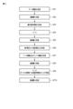
ゲート電極を形成し、前記ゲート電極を覆う第1絶縁膜を形成し、前記ゲート電極の上方において、前記第1絶縁膜に接する島状の酸化物半導体を形成し、前記酸化物半導体を覆う第2絶縁膜を形成し、前記第2絶縁膜において、前記酸化物半導体まで貫通した第1開口及び第2開口を形成し、前記第1開口において前記酸化物半導体に接するソース電極を形成し、前記第2開口において前記酸化物半導体に接するドレイン電極を形成し、前記ソース電極及び前記ドレイン電極を覆う第3絶縁膜を形成し、前記ソース電極と前記ドレイン電極との間において、前記第3絶縁膜から前記第2絶縁膜を介して前記酸化物半導体に酸素を供給し、チャネル領域を形成する。
共通電極CEは、複数の画素PXに亘って配置されている。共通電極CEは、所定電圧が供給される電圧供給部Vcomに接続されている。
なお、ここで説明した電気泳動表示装置は、モノクロ仕様に限定されるわけではなく、赤色粒子、緑色粒子、青色粒子を含む複数のカラー粒子を電気泳動法で動作させるカラー仕様にも適用できる。特にカラー仕様の場合、高い電圧を印加することで、元々遅い電気泳動速度を向上でき、カラー画面の高速書換えが可能となる利点がある。
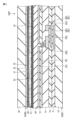
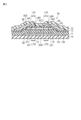
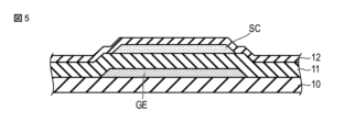
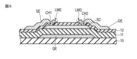
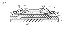
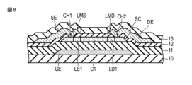
ソース電極SEは、絶縁膜12の第1開口CH1において、酸化物半導体SCに接している。ドレイン電極DEは、絶縁膜12の第2開口CH2において、酸化物半導体SCに接している。
一方で、チャネル領域C1に隣接する領域では、ソース電極SE及びドレイン電極DEが酸素供給路における障壁となるため、ソース電極SEとドレイン電極DEとの間の領域と比較して、酸素供給量が低減される。このため、酸化物半導体SCのうち、チャネル領域C1に隣接する領域では、チャネル領域C1よりも酸化の度合いが小さく制限され、低抵抗領域LS1及びLD1が形成される。したがって、信頼性の高い酸化物半導体トランジスタを容易に形成することができる。
ストレス付与前とストレス付与後とでVg-Id特性を比較すると、ドレイン電流が出力されるゲート電圧(しきい値電圧)が大きくシフトしていることが確認された。ここで、ソース-ドレイン間の電圧を30Vに設定した場合(C)のVg-Id特性に着目し、ストレス付与前とストレス付与後におけるしきい値電圧の差をシフト量ΔVthと定義する。
尚、本実施形態では、要求される駆動電圧の高い電気泳動表示装置について説明したが、本発明は、通常の液晶ディスプレイより高い印加電圧が必要とされる液晶ディスプレイや、高速応答用の液晶ディスプレイとして、ポリマー分散型液晶やそれを用いた高速駆動ディスプレイへの適用も可能である。
10…絶縁基板 11…絶縁膜(第1絶縁膜) 12…絶縁膜(第2絶縁膜)
13…絶縁膜(第3絶縁膜)
TR…トランジスタ(酸化物半導体トランジスタ)
GE…ゲート電極 SE…ソース電極 DE…ドレイン電極
SC…酸化物半導体 C1…チャネル領域 LS1、LD1…低抵抗領域
CH1…第1開口 CH2…第2開口
Claims (8)
- ゲート電極を形成し、
前記ゲート電極を覆う第1絶縁膜を形成し、
前記ゲート電極の上方において、前記第1絶縁膜に接する島状の酸化物半導体を形成し、
前記酸化物半導体を覆う第2絶縁膜を形成し、
前記第2絶縁膜において、前記酸化物半導体まで貫通した第1開口及び第2開口を形成し、
前記第1開口において前記酸化物半導体に接するソース電極を形成し
前記第2開口において前記酸化物半導体に接するドレイン電極を形成し、
前記ソース電極及び前記ドレイン電極を覆う第3絶縁膜を形成し、
前記ソース電極と前記ドレイン電極との間において、前記第3絶縁膜から前記第2絶縁膜を介して前記酸化物半導体に酸素を供給し、チャネル領域を形成する、半導体装置の製造方法。 - さらに、前記酸化物半導体のうち、前記第1開口と前記第2開口との間における前記第2絶縁膜及び前記ソース電極の積層体と重畳する領域、及び、前記第1開口と前記第2開口との間における前記第2絶縁膜及び前記ドレイン電極の積層体と重畳する領域において、前記第3絶縁膜から前記第2絶縁膜を介して前記酸化物半導体に酸素を供給し、前記チャネル領域よりも低抵抗の低抵抗領域を形成する、請求項1に記載の半導体装置の製造方法。
- 前記チャネル領域の形成、及び、前記低抵抗領域の形成は、前記第3絶縁膜を形成した後のベークによって行う、請求項2に記載の半導体装置の製造方法。
- 前記第2絶縁膜及び前記第3絶縁膜は、シリコン酸化物によって形成されている、請求項3に記載の半導体装置の製造方法。
- 前記第1絶縁膜のうち、少なくとも前記酸化物半導体の下面に接する薄膜は、シリコン酸化物によって形成されている、請求項4に記載の半導体装置の製造方法。
- 前記第1開口と前記第2開口との間における前記第2絶縁膜及び前記ソース電極の積層体の長さ、及び、前記第1開口と前記第2開口との間における前記第2絶縁膜及び前記ドレイン電極の積層体の長さは、1.5μm以上である、請求項2に記載の半導体装置の製造方法。
- 前記低抵抗領域の長さは、1.5μm以上である、請求項6に記載の半導体装置の製造方法。
- 前記酸化物半導体の膜厚は、60nm以上である、請求項7に記載の半導体装置の製造方法。
Priority Applications (2)
| Application Number | Priority Date | Filing Date | Title |
|---|---|---|---|
| JP2020181414A JP7516210B2 (ja) | 2020-10-29 | 2020-10-29 | 半導体装置の製造方法 |
| US17/511,633 US12068399B2 (en) | 2020-10-29 | 2021-10-27 | Semiconductor device manufacturing method |
Applications Claiming Priority (1)
| Application Number | Priority Date | Filing Date | Title |
|---|---|---|---|
| JP2020181414A JP7516210B2 (ja) | 2020-10-29 | 2020-10-29 | 半導体装置の製造方法 |
Publications (2)
| Publication Number | Publication Date |
|---|---|
| JP2022072129A JP2022072129A (ja) | 2022-05-17 |
| JP7516210B2 true JP7516210B2 (ja) | 2024-07-16 |
Family
ID=81380489
Family Applications (1)
| Application Number | Title | Priority Date | Filing Date |
|---|---|---|---|
| JP2020181414A Active JP7516210B2 (ja) | 2020-10-29 | 2020-10-29 | 半導体装置の製造方法 |
Country Status (2)
| Country | Link |
|---|---|
| US (1) | US12068399B2 (ja) |
| JP (1) | JP7516210B2 (ja) |
Citations (4)
| Publication number | Priority date | Publication date | Assignee | Title |
|---|---|---|---|---|
| JP2017084435A (ja) | 2015-10-30 | 2017-05-18 | 株式会社半導体エネルギー研究所 | 半導体装置、電子機器 |
| JP2018185397A (ja) | 2017-04-25 | 2018-11-22 | 株式会社ジャパンディスプレイ | 表示装置及びその製造方法 |
| JP2020113779A (ja) | 2014-02-28 | 2020-07-27 | 株式会社半導体エネルギー研究所 | 半導体装置 |
| JP2020167188A (ja) | 2019-03-28 | 2020-10-08 | 株式会社ジャパンディスプレイ | 表示装置および表示装置の製造方法 |
Family Cites Families (9)
| Publication number | Priority date | Publication date | Assignee | Title |
|---|---|---|---|---|
| US8541266B2 (en) * | 2011-04-01 | 2013-09-24 | Semiconductor Energy Laboratory Co., Ltd. | Method for manufacturing semiconductor device |
| JP6329762B2 (ja) * | 2012-12-28 | 2018-05-23 | 株式会社半導体エネルギー研究所 | 半導体装置 |
| WO2015029286A1 (ja) * | 2013-08-27 | 2015-03-05 | パナソニック株式会社 | 薄膜トランジスタ基板の製造方法及び薄膜トランジスタ基板 |
| US10121898B2 (en) * | 2014-05-09 | 2018-11-06 | Joled Inc. | Thin-film transistor substrate and method of manufacturing the same |
| JP6358596B2 (ja) * | 2014-11-27 | 2018-07-18 | 株式会社Joled | 薄膜トランジスタ基板の製造方法 |
| WO2016108122A1 (en) * | 2014-12-29 | 2016-07-07 | Semiconductor Energy Laboratory Co., Ltd. | Semiconductor device and display device having semiconductor device |
| CN107406966B (zh) * | 2015-03-03 | 2020-11-20 | 株式会社半导体能源研究所 | 氧化物半导体膜、包括该氧化物半导体膜的半导体装置以及包括该半导体装置的显示装置 |
| JP6827270B2 (ja) | 2016-03-28 | 2021-02-10 | 株式会社ジャパンディスプレイ | 半導体装置の作製方法 |
| JP2020129635A (ja) | 2019-02-12 | 2020-08-27 | 株式会社ジャパンディスプレイ | 半導体装置および半導体装置の製造方法 |
-
2020
- 2020-10-29 JP JP2020181414A patent/JP7516210B2/ja active Active
-
2021
- 2021-10-27 US US17/511,633 patent/US12068399B2/en active Active
Patent Citations (4)
| Publication number | Priority date | Publication date | Assignee | Title |
|---|---|---|---|---|
| JP2020113779A (ja) | 2014-02-28 | 2020-07-27 | 株式会社半導体エネルギー研究所 | 半導体装置 |
| JP2017084435A (ja) | 2015-10-30 | 2017-05-18 | 株式会社半導体エネルギー研究所 | 半導体装置、電子機器 |
| JP2018185397A (ja) | 2017-04-25 | 2018-11-22 | 株式会社ジャパンディスプレイ | 表示装置及びその製造方法 |
| JP2020167188A (ja) | 2019-03-28 | 2020-10-08 | 株式会社ジャパンディスプレイ | 表示装置および表示装置の製造方法 |
Also Published As
| Publication number | Publication date |
|---|---|
| JP2022072129A (ja) | 2022-05-17 |
| US20220140117A1 (en) | 2022-05-05 |
| US12068399B2 (en) | 2024-08-20 |
Similar Documents
| Publication | Publication Date | Title |
|---|---|---|
| CN114664865B (zh) | 显示装置 | |
| CN102237412B (zh) | 图像显示装置及其制造方法 | |
| JP2010003910A (ja) | 表示素子 | |
| US7079199B2 (en) | Liquid crystal display panel | |
| US7636145B2 (en) | Display apparatus and method of manufacturing the same | |
| CN100505315C (zh) | 薄膜晶体管和图像显示装置 | |
| CN107507835A (zh) | 半导体装置及显示装置 | |
| CN110007505A (zh) | 显示设备 | |
| US10209592B2 (en) | Active matrix substrate, display device and display device manufacturing method | |
| US10067393B2 (en) | Thin film display panel and liquid crystal display device including the same | |
| JP2010145875A (ja) | 液晶表示装置及びその製造方法 | |
| JP2008225034A (ja) | 電気光学装置及び電子機器 | |
| JP7516210B2 (ja) | 半導体装置の製造方法 | |
| KR20050068187A (ko) | 액정표시장치 | |
| JP7520690B2 (ja) | 表示装置 | |
| KR102938368B1 (ko) | 표시 장치 | |
| JP2002189428A (ja) | アレイ基板及びそれを用いた液晶表示装置 | |
| US12563899B2 (en) | Display panel and display apparatus including the same | |
| KR101151797B1 (ko) | 액정표시장치용 기판 및 그 제조방법 | |
| JP7446774B2 (ja) | 半導体基板及び表示装置 | |
| JP2002297058A (ja) | アクティブマトリクス型表示装置 | |
| KR101202534B1 (ko) | 액정표시장치 및 그의 제조방법 | |
| KR101463026B1 (ko) | 액정표시장치 및 그 제조방법 | |
| JP2026003247A (ja) | 表示装置 | |
| US10490772B2 (en) | Display device |
Legal Events
| Date | Code | Title | Description |
|---|---|---|---|
| A621 | Written request for application examination |
Free format text: JAPANESE INTERMEDIATE CODE: A621 Effective date: 20230907 |
|
| A977 | Report on retrieval |
Free format text: JAPANESE INTERMEDIATE CODE: A971007 Effective date: 20240528 |
|
| A131 | Notification of reasons for refusal |
Free format text: JAPANESE INTERMEDIATE CODE: A131 Effective date: 20240604 |
|
| A521 | Request for written amendment filed |
Free format text: JAPANESE INTERMEDIATE CODE: A523 Effective date: 20240611 |
|
| TRDD | Decision of grant or rejection written | ||
| A01 | Written decision to grant a patent or to grant a registration (utility model) |
Free format text: JAPANESE INTERMEDIATE CODE: A01 Effective date: 20240625 |
|
| A61 | First payment of annual fees (during grant procedure) |
Free format text: JAPANESE INTERMEDIATE CODE: A61 Effective date: 20240703 |
|
| R150 | Certificate of patent or registration of utility model |
Ref document number: 7516210 Country of ref document: JP Free format text: JAPANESE INTERMEDIATE CODE: R150 |
|
| S111 | Request for change of ownership or part of ownership |
Free format text: JAPANESE INTERMEDIATE CODE: R313113 |
|
| R350 | Written notification of registration of transfer |
Free format text: JAPANESE INTERMEDIATE CODE: R350 |