WO2020195142A1 - パワー半導体装置 - Google Patents
パワー半導体装置 Download PDFInfo
- Publication number
- WO2020195142A1 WO2020195142A1 PCT/JP2020/003318 JP2020003318W WO2020195142A1 WO 2020195142 A1 WO2020195142 A1 WO 2020195142A1 JP 2020003318 W JP2020003318 W JP 2020003318W WO 2020195142 A1 WO2020195142 A1 WO 2020195142A1
- Authority
- WO
- WIPO (PCT)
- Prior art keywords
- power semiconductor
- semiconductor element
- conductor
- semiconductor device
- insulating substrate
- Prior art date
- Legal status (The legal status is an assumption and is not a legal conclusion. Google has not performed a legal analysis and makes no representation as to the accuracy of the status listed.)
- Ceased
Links
Images






Classifications
-
- H—ELECTRICITY
- H10—SEMICONDUCTOR DEVICES; ELECTRIC SOLID-STATE DEVICES NOT OTHERWISE PROVIDED FOR
- H10W—GENERIC PACKAGES, INTERCONNECTIONS, CONNECTORS OR OTHER CONSTRUCTIONAL DETAILS OF DEVICES COVERED BY CLASS H10
- H10W90/00—Package configurations
-
- H—ELECTRICITY
- H10—SEMICONDUCTOR DEVICES; ELECTRIC SOLID-STATE DEVICES NOT OTHERWISE PROVIDED FOR
- H10W—GENERIC PACKAGES, INTERCONNECTIONS, CONNECTORS OR OTHER CONSTRUCTIONAL DETAILS OF DEVICES COVERED BY CLASS H10
- H10W72/00—Interconnections or connectors in packages
- H10W72/071—Connecting or disconnecting
- H10W72/073—Connecting or disconnecting of die-attach connectors
- H10W72/07351—Connecting or disconnecting of die-attach connectors characterised by changes in properties of the die-attach connectors during connecting
- H10W72/07354—Connecting or disconnecting of die-attach connectors characterised by changes in properties of the die-attach connectors during connecting changes in dispositions
-
- H—ELECTRICITY
- H10—SEMICONDUCTOR DEVICES; ELECTRIC SOLID-STATE DEVICES NOT OTHERWISE PROVIDED FOR
- H10W—GENERIC PACKAGES, INTERCONNECTIONS, CONNECTORS OR OTHER CONSTRUCTIONAL DETAILS OF DEVICES COVERED BY CLASS H10
- H10W72/00—Interconnections or connectors in packages
- H10W72/30—Die-attach connectors
- H10W72/341—Dispositions of die-attach connectors, e.g. layouts
- H10W72/347—Dispositions of multiple die-attach connectors
-
- H—ELECTRICITY
- H10—SEMICONDUCTOR DEVICES; ELECTRIC SOLID-STATE DEVICES NOT OTHERWISE PROVIDED FOR
- H10W—GENERIC PACKAGES, INTERCONNECTIONS, CONNECTORS OR OTHER CONSTRUCTIONAL DETAILS OF DEVICES COVERED BY CLASS H10
- H10W90/00—Package configurations
- H10W90/701—Package configurations characterised by the relative positions of pads or connectors relative to package parts
- H10W90/751—Package configurations characterised by the relative positions of pads or connectors relative to package parts of bond wires
- H10W90/753—Package configurations characterised by the relative positions of pads or connectors relative to package parts of bond wires between laterally-adjacent chips
Definitions
- the present invention relates to a power semiconductor device.
- Power semiconductor devices are applied to power conversion devices that control motors for driving vehicles. It is also applied not only to vehicle driving but also to power conversion devices that control motors of railways, elevators, industrial equipment, aircraft, and the like.
- Patent Document 1 discloses a power semiconductor device that cools a plurality of semiconductor elements constituting the upper and lower arms of the power conversion device from both sides.
- thermal warpage may occur in the laminated structure portion with the insulating substrate, causing peeling or the like in the laminated structure portion, which may reduce reliability.
- the power semiconductor device is connected to the first semiconductor element and the second semiconductor element, and the first semiconductor element and the second semiconductor element are arranged side by side so as to be separated from each other with a gap region between them.
- a first insulating substrate to be laminated is provided, and the first conductor has a penetrating portion formed in a portion corresponding to the gap region.
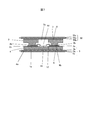
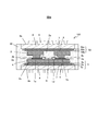
- FIG. 1 is a cross-sectional view of the power semiconductor device 100.
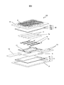
- FIG. 2 is a developed perspective view of the power semiconductor device 100.
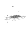
- FIG. 3 is an external view of the power semiconductor device 100. Note that FIG. 1 shows a cross-sectional view taken along the line AA'in FIG.
- the power semiconductor element 1a and the power semiconductor element 1b are arranged side by side. That is, the power semiconductor element 1a and the power semiconductor element 1b are arranged side by side so as to be separated from each other with the gap region 30 interposed therebetween.
- Each electrode of the power semiconductor element 1a and the power semiconductor element 1b is sandwiched between the first conductor 3 and the second conductor 4 arranged so as to face each electrode surface.
- the first power semiconductor element 1a and the second power semiconductor element 1b are joined to the first conductor 3 and the second conductor 4 by connecting materials 2a and 2b, respectively.
- the first conductor 3 and the second conductor 4 are formed of, for example, copper, a copper alloy, aluminum, an aluminum alloy, or the like.
- the connecting materials 2a and 2b are formed of a solder material, a sintered material, or the like.
- the first conductor 3 has a penetrating portion 3a formed in a portion corresponding to the gap region 30. Further, a wiring board 11 is provided between the first power semiconductor element 1a and the second power semiconductor element 1b on the second conductor 4, that is, in the gap region 30.
- the wiring substrate 11 has, for example, a pattern wiring in which a copper electrode is provided on a glass epoxy resin, and is electrically connected to the first power semiconductor element 1a and the second power semiconductor element 1b by a wiring 12.
- a wiring 12 for example, an aluminum wire or a copper wire can be used.
- the insulating substrate 50 is laminated on the surface opposite to the surface of the first conductor 3 connected to the first power semiconductor element 1a and the second power semiconductor element 1b.
- the insulating substrate 50 is composed of an insulating member 50a, a first conductor layer 50b, and a second conductor layer 50c.
- the first conductor layer 50b is arranged on one surface of the insulating member 50a, and the second conductor layer 50c is arranged on the other surface.
- the surface of the first conductor 3 opposite to the surface connected to the first power semiconductor element 1a and the second power semiconductor element 1b is connected to the first conductor layer 50b via the connecting material 6.
- the second conductor layer 50c is connected to the heat radiating member 8 via the connecting material 7.
- a heat radiating fin 9 is formed on the surface of the heat radiating member 8.
- the insulating substrate 5 is laminated on the second conductor 4.
- the insulating substrate 5 is composed of an insulating member 5a, a first conductor layer 5b, and a second conductor layer 5c.
- the first conductor layer 5b is arranged on one surface of the insulating member 5a, and the second conductor layer 5c is arranged on the other surface.
- the surface of the second conductor 4 opposite to the surface connected to the first power semiconductor element 1a and the second power semiconductor element 1b is connected to the first conductor layer 5b via the connecting material 6.
- the second conductor layer 5c is connected to the heat radiating member 8 via the connecting material 7.
- a heat radiating fin 9 is formed on the surface of the heat radiating member 8.
- the insulating member 5a and the insulating member 50a conduct the heat generated from the first power semiconductor element 1a and the second power semiconductor element 1b to the heat radiating member 8, and have high thermal conductivity and high insulation withstand voltage.
- a ceramic material is used as the material.
- ceramic materials such as aluminum oxide (alumina), aluminum nitride, and silicon nitride are used.
- the connecting material 6 and the connecting material 7 are formed of a solder material, a sintered material, or the like.
- the heat radiating member 8 and the heat radiating fin 9 are members having electrical conductivity, for example, a composite material such as Cu, Cu alloy, Cu-C, Cu-CuO, or a composite material such as Al, Al alloy, AlSiC, Al-C, etc. Is formed from.
- first power semiconductor elements 1a and five second power semiconductor elements 1b are provided in one row, and two rows are provided in parallel.
- Two first conductors 3, two second conductors 4, and two wiring boards 11 are provided corresponding to the first power semiconductor element 1a and the second power semiconductor element 1b provided in parallel in two rows.
- a penetrating portion 3a is provided in the first conductor 3 corresponding to the gap region between the first power semiconductor element 1a and the second power semiconductor element 1b shown by AA in FIG. ..
- the terminal 14 shown in FIG. 2 is connected to the first conductor layer 5b of the insulating substrate 5 and the first conductor layer 50b of the insulating substrate 50.
- FIG. 3 is an external view of the power semiconductor device 100. As shown in FIG. 3, except for the heat radiating surface 8a and the terminal 14 on which the heat radiating fins 9 are formed, the heat radiating surface 8a and the terminal 14 are sealed with the sealing resin 10.
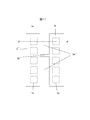
- FIG. 4 is a top view showing the first conductor 3. That is, it is a top view of only the first conductor 3 taken out and viewed from the connection surface side with the insulating substrate 50.
- the first conductor 3 is provided with a penetrating portion 3a.
- the penetrating portion 3a is provided elongated along the arrangement direction of the first power semiconductor element 1a and the second power semiconductor element 1b.
- the position of the penetrating portion 3a corresponds to the gap region 30 between the first power semiconductor element 1a and the second power semiconductor element 1b, that is, the wiring substrate between the first power semiconductor element 1a and the second power semiconductor element 1b. It is provided at a position facing the 11.
- the joint area between the insulating substrate 5 and the first conductor 3 can be reduced.
- the length of the first power semiconductor element 1a and the second power semiconductor element 1b in the arrangement direction is L10 and the length of the penetrating portion 3a is L11, it is desirable that L11 ⁇ L10.
- 5 to 8 are diagrams showing a manufacturing process of the power semiconductor device 100.
- the first power semiconductor element 1a and the second power semiconductor element 1b are connected to the second conductor 4 via a connecting material 2a.
- a wiring board 11 is provided on the second conductor 4, and a first power semiconductor element 1a and a second power semiconductor element 1b are arranged so as to sandwich the wiring board 11.
- the first power semiconductor element 1a and the second power semiconductor element 1b are each connected to the pattern wiring on the wiring board 11 by the wiring 12.
- the second conductor 4 is formed of, for example, copper, a copper alloy, aluminum, an aluminum alloy, or the like.
- the connecting material 2a is formed of a solder material, a sintered material, or the like.
- the first conductor 3 is placed on the surface opposite to the surface of the first power semiconductor element 1a and the second power semiconductor element 1b to which the second conductor 4 is connected via the connecting material 2b.
- the first conductor 3 is formed of, for example, copper, a copper alloy, aluminum, an aluminum alloy, or the like.
- the connecting material 2b is formed of a solder material, a sintered material, or the like.
- the first conductor 3 and the second conductor 4 are connected to the first conductor layer 50b of the insulating substrate 50 and the first conductor layer 5b of the insulating substrate 5 via the connecting material 6, respectively.
- the first conductor layer 5b is arranged on one surface of the insulating member 5a, and the second conductor layer 5c is arranged on the other surface.
- the insulating substrate 50 and the insulating substrate 5 may be connected to the first conductor 3 and the second conductor 4 at the same time. By connecting at the same time, symmetry can be maintained and warpage deformation during assembly can be suppressed.
- the heat radiating member 8 is connected to the insulating substrate 50 and the insulating substrate 5 via the connecting material 7. At this time, the heat radiating members 8 on both sides may be connected at the same time. By connecting at the same time, it is possible to suppress warpage deformation during assembly. Heat dissipation fins 9 are formed on the surface of the heat dissipation member 8. Finally, the heat radiating surface 8a on which the heat radiating fins 9 of the heat radiating member 8 are formed is sealed with the sealing resin 10.
- the wiring board 11 is provided between the first power semiconductor element 1a and the second power semiconductor element 1b.
- the distance between the first power semiconductor element 1a and the second power semiconductor element 1b becomes longer.
- the first power is provided by providing the penetrating portion 3a at a position facing the wiring board 11 between the first power semiconductor element 1a and the second power semiconductor element 1b of the first conductor 3.
- the lengths L1 and L2 in which only the first conductor 3 is connected to the insulating substrate 50, which is an insulating substrate, can be shortened.
- the region where only the first conductor 3 is connected to the insulating substrate 50 is reduced, so that thermal warpage can be suppressed, and the connecting material 2b at the interface between the first power semiconductor element 1a and the second conductor and the second
- the stress generated in the connecting material 2b at the interface between the power semiconductor element 1b and the second conductor is also reduced. Therefore, it is possible to prevent cracks and peeling of the laminated structure of the first conductor 3 and the insulating substrate 50, and it is possible to provide a highly reliable power semiconductor device.
- the power semiconductor device 100 when the power semiconductor device 100 is installed and used in a vehicle or the like, the power semiconductor device 100 repeatedly operates and stops, and as a result, repeatedly generates heat and cools. Since the power semiconductor device 100 repeatedly applies a large strain to the laminated portion of the insulating substrate and the conductor, there is a concern that the laminated portion may be peeled off.
- the penetrating portion 3a is provided at a position facing the wiring board 11 between the first power semiconductor element 1a and the second power semiconductor element 1b of the first conductor 3. As a result, the stress that occurs repeatedly is reduced, and the fatigue life is improved. As a result, a highly reliable power semiconductor device 100 can be realized.
- the shape of the heat radiating fin 9 of the heat radiating member 8 has been described with the example of a pin fin, other shapes such as straight fins and corrugated fins may be used.
- the sealing resin 10 includes the heat radiating member 8 and the heat radiating surface 8a is sealed, but the insulating substrate 5 may be resin-sealed. In this case, if the second conductor layer 50c of the insulating substrate 50 and the heat radiating member 8 are connected and the second conductor layer 5c of the insulating substrate 5 and the heat radiating member 8 are connected, the same effect can be obtained.
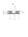
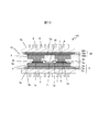
- FIG. 9 is a cross-sectional view of the power semiconductor device 100 similar to that shown in FIG.
- the width of the penetrating portion is L3 and the width of the wiring board 11 is L4, it is desirable that L3 ⁇ L4.
- the distance between the first power semiconductor element 1a and the second power semiconductor element 1b is L5. That is, when the side surface of the first power semiconductor element 1a on the wiring board 11 side is 1c and the side surface of the second power semiconductor element 1b on the wiring board side is 1d, the distance between the side surface 1c and the side surface 1d is L5. , L3 ⁇ L5.
- the first power semiconductor element 1a and the second power semiconductor elements 1b are provided, but the first power semiconductor element 1a and the second power It is sufficient that there is one or more semiconductor elements 1b each.
- the penetrating portion 3a may be provided at least between the first power semiconductor element 1a and the second power semiconductor element 1b. This has the same effect.
- FIG. 10 is a top view showing the first conductor 3'.
- the cross-sectional view of the power semiconductor device 100 in AA'in FIG. 10 including the first conductor 3' is the same as that in FIG. 1, and the developed perspective view of the power semiconductor device 100 including the first conductor 3'is shown in FIG. It is the same as 2.
- the first conductor 3'in the present embodiment is provided with a penetrating portion 3a'between the first power semiconductor element 1a and the second power semiconductor element 1b.
- a plurality of penetrating portions 3a' are provided in the arrangement direction of the first power semiconductor element 1a and the second power semiconductor element 1b.
- a connecting portion 3b'connecting between the first power semiconductor element side and the second power semiconductor element side of the first conductor 3' is provided at intervals of each first power semiconductor element 1a and each second power semiconductor element 1b.
- the length of the first power semiconductor element 1a and the second power semiconductor element 1b in the arrangement direction is L10'and the length of the penetrating portion 3a is L11', it is desirable that L11' ⁇ L10'. According to this embodiment, in addition to having the effect described in the first embodiment, an effect of reducing the electric resistance in the first conductor 3'can be obtained.
- FIG. 11 is a top view showing the first conductor 3 ′′.
- the cross-sectional view of the power semiconductor device 100 in AA'in FIG. 11 including the first conductor 3 ′′ is the same as that in FIG. 1, and a developed perspective view of the power semiconductor device 100 including the first conductor 3 ′′. Is the same as in FIG.
- the first conductor 3 ′′ in the present embodiment is provided with a connecting portion 3b ′′ connecting between the first power semiconductor element side and the second power semiconductor element side at only one place. There is.
- a penetrating portion 3a'' is formed between the first power semiconductor element 1a and the second power semiconductor element 1b excluding the connecting portion 3b''.
- the bonding area of the first conductor 3 ′′ connected to the insulating substrate 50 can be reduced, and the first conductor 3 ′′ can be made smaller. 3e on the 1-power semiconductor element side and 3f on the 2nd power semiconductor element side of the 1st conductor 3 ′′ can be freely deformed. Therefore, the thermal warpage of the laminated structure of the first conductor 3'' and the insulating substrate 50 can be further suppressed, and cracks and peeling of the laminated structure of the first conductor 3'' and the insulating substrate 50 can be prevented. It is possible to provide a highly reliable power semiconductor device.
- the number of parts is reduced by connecting the first conductor 3'' at at least one place instead of completely dividing it into two by 3e on the first power semiconductor element side and 3f on the second power semiconductor element side. Further, the height adjustment when connecting the first conductor 3'' and the insulating substrate 50 becomes easy.
- the sealing resin includes the heat radiating member 8 and the heat radiating surface 8a is sealed.
- the insulating substrates 5 and 50 may have a sealed structure. If the second conductor layers 5c and 50c of the insulating substrates 5 and 50 and the heat radiating member 8 are connected, the same effect can be obtained. Since other configurations are the same as those in FIG. 1, the same parts are designated by the same reference numerals and the description thereof will be omitted.
- the structure may be such that the heat radiation fins 9 are directly provided on the second conductor layers 5c and 50c. Since other configurations are the same as those in FIG. 1, the same parts are designated by the same reference numerals and the description thereof will be omitted.
- the power semiconductor device 100 includes a first power semiconductor element 1a and a second power semiconductor element 1b arranged side by side so as to be separated from each other with a gap region 30 interposed therebetween, and a first power semiconductor element 1a and a second power semiconductor element. Connected to the first conductor 3 and the second conductor 4 connected to 1b and arranged so as to sandwich the first power semiconductor element 1a and the second power semiconductor element 1b, and connected to the first power semiconductor element 1a and the second power semiconductor element 1b.
- An insulating substrate 5 laminated on a surface opposite to the surface of the first conductor 3 is provided, and the first conductor 3 has a penetrating portion 3a formed in a portion corresponding to the gap region 30.
- the present invention is not limited to the above-described embodiment, and other embodiments considered within the scope of the technical idea of the present invention are also included within the scope of the present invention as long as the features of the present invention are not impaired. .. Further, the configuration may be a combination of the above-described embodiments.
Landscapes
- Cooling Or The Like Of Semiconductors Or Solid State Devices (AREA)
Abstract
第1導体3には、間隙領域30に対応する部分に貫通部3aが形成されている。第1導体3には、絶縁基板50が積層される。第1導体3に貫通部3aをもうけることにより、絶縁基板50に第1導体3のみが接続される領域が減少するため、熱反りを抑制することができ、第1パワー半導体素子1aと第2導体界面の接続材2bや、第2パワー半導体素子1bと第2導体界面の接続材2bに発生する応力も低減される。したがって、第1導体3と絶縁基板50との積層構造のクラックやはく離を防止することができ、信頼性の高いパワー半導体装置を提供できる。
Description
本発明は、パワー半導体装置に関する。
パワー半導体装置は、車両駆動用のモータを制御する電力変換装置に適用されている。また、車両駆動用のみならず、鉄道、エレベータ、産業機器、航空機等のモータを制御する電力変換装置にも適用されている。
例えば、ハイブリッド自動車や電気自動車向けの電力変換装置では、充電時間を短縮する目的で動作電圧の高いパワー半導体装置が望まれている。動作電圧の高いパワー半導体装置では絶縁基板として絶縁耐圧の高いセラミック材料を使用する場合がある。一方で、小型化や、冷却性能の要求により両面直接冷却方式のパワー半導体装置が知られている。特許文献1には、電力変換装置の上下アームを構成する複数の半導体素子を両面から冷却するパワー半導体装置が開示されている。
パワー半導体装置の製造過程で絶縁基板との積層構造部分に熱反りが発生し、積層構造部分に剥離等が生じて信頼性が低下する虞がある。
本発明によるパワー半導体装置は、互いに間隙領域を介して離間して並べて配置される第1半導体素子及び第2半導体素子と、前記第1半導体素子及び前記第2半導体素子に接続され、前記第1半導体素子及び前記第2半導体素子を挟んで配置される第1導体および第2導体と、前記第1半導体素子及び前記第2半導体素子に接続された前記第1導体の面とは反対の面に積層される第1絶縁基板と、を備え、前記第1導体は、前記間隙領域に対応する部分に貫通部が形成される。
本発明によれば、絶縁基板との積層構造部分の剥離等を防止して信頼性の高いパワー半導体装置を提供できる。
[第1の実施形態]
本実施形態に係るパワー半導体装置100について、図1~図9を参照して説明する。図1は、パワー半導体装置100の断面図である。図2は、パワー半導体装置100の展開斜視図である。図3は、パワー半導体装置100の外観図である。なお、図1は、図2中のA-A’における断面図を示している。
本実施形態に係るパワー半導体装置100について、図1~図9を参照して説明する。図1は、パワー半導体装置100の断面図である。図2は、パワー半導体装置100の展開斜視図である。図3は、パワー半導体装置100の外観図である。なお、図1は、図2中のA-A’における断面図を示している。
図1に示すように、パワー半導体装置100は、パワー半導体素子1aおよびパワー半導体素子1bが並べて配置される。すなわち、パワー半導体素子1aおよびパワー半導体素子1bは、互いに間隙領域30を介して離間して並べて配置される。パワー半導体素子1aおよびパワー半導体素子1bの各電極は、それぞれの電極面に対向して配置される第1導体3と第2導体4とによって挟まれる。第1パワー半導体素子1aおよび第2パワー半導体素子1bは、第1導体3及び第2導体4とそれぞれ接続材2a、2bによって接合される。第1導体3、第2導体4は、例えば、銅、銅合金、あるいはアルミニウム、アルミニウム合金などにより形成されている。接続材2a、2bは、はんだ材、焼結材などにより形成されている。
第1導体3には、間隙領域30に対応する部分に貫通部3aが形成されている。また、第2導体4上の第1パワー半導体素子1aと第2パワー半導体素子1bとの間、すなわち間隙領域30には、配線基板11が設けられている。配線基板11は、例えばガラスエポキシ樹脂上に銅電極が設けられたパターン配線を有しており、第1パワー半導体素子1aおよび第2パワー半導体素子1bと配線12で電気的に接続されている。配線12は例えばアルミワイヤや銅ワイヤなどを用いることができる。
第1導体3には、第1パワー半導体素子1aおよび第2パワー半導体素子1bに接続された第1導体3の面とは反対の面に絶縁基板50が積層される。絶縁基板50は、絶縁部材50a、第1導体層50b及び第2導体層50cから構成され、絶縁部材50aの一面に第1導体層50bが配置され、他面に第2導体層50cが配置される。第1導体3の第1パワー半導体素子1aおよび第2パワー半導体素子1bと接続する面と反対の面は、接続材6を介して第1導体層50bと接続される。第2導体層50cは、接続材7を介して放熱部材8と接続される。放熱部材8の表面には放熱フィン9が形成される。
第2導体4には絶縁基板5が積層される。絶縁基板5は、絶縁部材5a、第1導体層5b及び第2導体層5cから構成され、絶縁部材5aの一面に第1導体層5bが配置され、他面に第2導体層5cが配置される。第2導体4の第1パワー半導体素子1aおよび第2パワー半導体素子1bと接続する面と反対の面は、接続材6を介して第1導体層5bと接続される。第2導体層5cは、接続材7を介して放熱部材8と接続される。放熱部材8の表面には放熱フィン9が形成される。
絶縁部材5aおよび絶縁部材50aは、第1パワー半導体素子1aと第2パワー半導体素子1bから発生する熱を放熱部材8に熱伝導するものであり、熱伝導率が高く、かつ、絶縁耐圧が大きい材料であるセラミック材料を用いる。例えば、酸化アルミニウム(アルミナ)、窒化アルミニウム、窒化ケイ素等のセラミック材料を用いる。接続材6および接続材7は、はんだ材や焼結材などから形成されている。放熱部材8および放熱フィン9は、電気伝導性を有する部材、例えばCu、Cu合金、Cu-C、Cu-CuOなどの複合材、あるいはAl、Al合金、AlSiC、Al-Cなどの複合材などから形成されている。
図2に示すように、第1パワー半導体素子1aと第2パワー半導体素子1bは、それぞれ1列に5個設けられ、さらに2列並列に設けられている。2列並列に設けられた第1パワー半導体素子1aと第2パワー半導体素子1bに対応して、第1導体3、第2導体4、配線基板11がそれぞれ2個設けられる。そして、図2中のA-A’で示す第1パワー半導体素子1aと第2パワー半導体素子1bとの間の間隙領域に対応して、第1導体3には貫通部3aが設けられている。図2に示す端子14は、絶縁基板5の第1導体層5b、および絶縁基板50の第1導体層50bに接続される。
図3は、パワー半導体装置100の外観図である。図3に示すように、放熱フィン9が形成されている放熱面8a及び端子14以外は、封止樹脂10で封止されている。
図4は、第1導体3を示す上面図である。すなわち、第1導体3のみを取り出し、絶縁基板50との接続面側からみた上面図である。図4に示すように、第1導体3には貫通部3aが設けられている。貫通部3aは、第1パワー半導体素子1aおよび第2パワー半導体素子1bの配列方向に沿って細長く設けられている。貫通部3aの位置は、第1パワー半導体素子1aと第2パワー半導体素子1bの間の間隙領域30に対応して、すなわち第1パワー半導体素子1aおよび第2パワー半導体素子1bの間の配線基板11に対向する位置に設けられている。このように第1導体3に貫通部3aを設けることにより、絶縁基板5と第1導体3との接合面積を小さくすることができる。ここで、第1パワー半導体素子1aと第2パワー半導体素子1bの配列方向の長さをL10、貫通部3aの長さをL11とした場合、L11≧L10とすることが望ましい。
図5~図8は、パワー半導体装置100の製造工程を示す図である。
まず、図5に示すように、第1パワー半導体素子1aと第2パワー半導体素子1bが第2導体4に接続材2aを介して接続される。第2導体4には配線基板11が設けられており、この配線基板11を挟むように第1パワー半導体素子1aと第2パワー半導体素子1bが配置されている。第1パワー半導体素子1aと第2パワー半導体素子1bはそれぞれ配線12で配線基板11上のパターン配線に接続される。第2導体4は、例えば、銅、銅合金、あるいはアルミニウム、アルミニウム合金などにより形成される。接続材2aは、はんだ材または焼結材などにより形成されている。
まず、図5に示すように、第1パワー半導体素子1aと第2パワー半導体素子1bが第2導体4に接続材2aを介して接続される。第2導体4には配線基板11が設けられており、この配線基板11を挟むように第1パワー半導体素子1aと第2パワー半導体素子1bが配置されている。第1パワー半導体素子1aと第2パワー半導体素子1bはそれぞれ配線12で配線基板11上のパターン配線に接続される。第2導体4は、例えば、銅、銅合金、あるいはアルミニウム、アルミニウム合金などにより形成される。接続材2aは、はんだ材または焼結材などにより形成されている。
次に、図6に示すように、第1パワー半導体素子1aと第2パワー半導体素子1bの第2導体4が接続されている面と反対の面に、接続材2bを介して第1導体3を接続する。第1導体3は、例えば、銅、銅合金、あるいはアルミニウム、アルミニウム合金などにより形成される。接続材2bは、はんだ材または焼結材などにより形成される。
次に、図7に示すように、第1導体3及び第2導体4が、接続材6を介してそれぞれ絶縁基板50の第1導体層50b、絶縁基板5の第1導体層5bに接続される。絶縁基板5は、絶縁部材5aの一面に第1導体層5bが配置され、他面に第2導体層5cが配置される。なお、絶縁基板50と絶縁基板5を同時に、第1導体3および第2導体4に接続してもよい。同時に接続することで、対称性を保つことができ、組立時の反り変形を抑制することができる。
次に、図8に示すように、放熱部材8は、絶縁基板50および絶縁基板5に接続材7を介して、接続される。このとき、両面の放熱部材8を同時に接続してもよい。同時に接続することにより、組立時の反り変形を抑制することができる。放熱部材8の表面には放熱フィン9が形成されている。そして最後に、放熱部材8の放熱フィン9が形成されている放熱面8a以外は、封止樹脂10で封止される。
一般に、SiCチップを使用したパワー半導体素子を複数並列駆動させるパワー半導体装置の場合、パワー半導体素子のゲート配線を接続するための配線基板を設ける必要がある。具体的には、第1パワー半導体素子1aと第2パワー半導体素子1bの間に配線基板11が設けられる。これにより、第1パワー半導体素子1aと第2パワー半導体素子1bの間の距離が長くなる。第1導体3に貫通部3aを設けない場合、パワー半導体装置100の製造工程において高温で接続し室温まで冷却する過程で、絶縁基板と導体との線膨張係数差により、絶縁基板と導体の積層構造の反り変形が大きくなる。これにより、接合面積の小さい第1パワー半導体素子1aと第2導体界面の接続材2bや、第2パワー半導体素子1bと第2導体界面の接続材2bに応力が発生し、クラックが発生しやすくなる。特にパワー半導体素子の両面に第1導体3および第2導体4を接続し、さらにその外側に絶縁基板を接続する両面冷却構造のパワー半導体装置では、第1導体3および第2導体4と絶縁基板の積層構造の熱反りによって、積層構造部分に剥離が生じて信頼性が低下する虞がある。
しかし、本実施形態のように、第1導体3の第1パワー半導体素子1aと第2パワー半導体素子1bの間の配線基板11に対向する位置に、貫通部3aを設けることにより、第1パワー半導体素子1aと第2パワー半導体素子1bの間において、絶縁基板である絶縁基板50に第1導体3のみが接続される長さL1、L2(図9参照)を短くすることができる。これにより、絶縁基板50に第1導体3のみが接続される領域が減少するため、熱反りを抑制することができ、第1パワー半導体素子1aと第2導体界面の接続材2bや、第2パワー半導体素子1bと第2導体界面の接続材2bに発生する応力も低減される。したがって、第1導体3と絶縁基板50との積層構造のクラックやはく離を防止することができ、信頼性の高いパワー半導体装置を提供できる。
さらに、パワー半導体装置100を車両等に設置して使用した場合、パワー半導体装置100は、動作、停止を繰り返し、その結果、発熱と冷却を繰り返す。パワー半導体装置100は、絶縁基板と導体の積層部に繰り返し大きな歪み加わるため、積層部のはく離等が懸念される。本実施形態では、第1導体3の第1パワー半導体素子1aと第2パワー半導体素子1bの間の配線基板11に対向する位置に、貫通部3aを設ける。これにより、繰り返し発生する応力が減少し、疲労寿命が向上する。これにより信頼性の高いパワー半導体装置100が実現できる。
なお、放熱部材8の放熱フィン9の形状をピンフィンの例で説明したが、他の形状、例えばストレートフィンやコルゲートフィンであっても良い。また、本説明では、封止樹脂10が放熱部材8を含み、放熱面8a以外が封止された例を示したが、絶縁基板5までが樹脂封止された構造であってもよい。この場合、絶縁基板50の第2導体層50cと放熱部材8とが接続され、絶縁基板5の第2導体層5cと放熱部材8とが接続されていれば、同様の効果が得られる。
図9は、図1と同様のパワー半導体装置100の断面図であるが、貫通部3a他の幅を表記した図である。
図9に示すように、貫通部の幅をL3、配線基板11の幅をL4とした場合、L3≧L4とすることが望ましい。さらに第1パワー半導体素子1aと第2パワー半導体素子1b間の距離をL5とする。すなわち、第1パワー半導体素子1aの配線基板11側の側面を1cとし、第2パワー半導体素子1bの配線基板側の側面を1dとした場合に、側面1cと側面1dとの距離をL5とすると、L3≦L5とすることが望ましい。
図9に示すように、貫通部の幅をL3、配線基板11の幅をL4とした場合、L3≧L4とすることが望ましい。さらに第1パワー半導体素子1aと第2パワー半導体素子1b間の距離をL5とする。すなわち、第1パワー半導体素子1aの配線基板11側の側面を1cとし、第2パワー半導体素子1bの配線基板側の側面を1dとした場合に、側面1cと側面1dとの距離をL5とすると、L3≦L5とすることが望ましい。
本実施形態においては、図2に示したように第1パワー半導体素子1aを5個、第2パワー半導体素子1bを5個備えた例を示したが、第1パワー半導体素子1a、第2パワー半導体素子1bがそれぞれ1つ以上あればよい。そして、貫通部3aは少なくとも第1パワー半導体素子1aと第2パワー半導体素子1bの間に設けられていればよい。これにより同様の効果が得られる。
[第2の実施形態]
第2の実施形態について、図10を参照して説明する。図10は、第1導体3’を示す上面図である。なお、第1導体3’を含む図10中のA-A’におけるパワー半導体装置100の断面図は図1と同様であり、第1導体3’を含むパワー半導体装置100の展開斜視図は図2と同様である。
第2の実施形態について、図10を参照して説明する。図10は、第1導体3’を示す上面図である。なお、第1導体3’を含む図10中のA-A’におけるパワー半導体装置100の断面図は図1と同様であり、第1導体3’を含むパワー半導体装置100の展開斜視図は図2と同様である。
本実施形態における第1導体3’は、図10に示すように、第1パワー半導体素子1aと第2パワー半導体素子1bとの間には貫通部3a’が設けられている。貫通部3a’は、第1パワー半導体素子1aおよび第2パワー半導体素子1bの配列方向に複数個設けられている。第1導体3’における第1パワー半導体素子側と第2パワー半導体素子側の間をつなぐ接続部3b’が各第1パワー半導体素子1aおよび各第2パワー半導体素子1bの間隔毎に設けられている。
ここで、第1パワー半導体素子1aと第2パワー半導体素子1bの配列方向における長さをL10’、貫通部3aの長さをL11’とした場合、L11’≧L10’とすることが望ましい。
本実施形態によれば、第1の実施形態で述べた効果を有する他に、第1導体3’における電気抵抗を低減できる効果が得られる。
本実施形態によれば、第1の実施形態で述べた効果を有する他に、第1導体3’における電気抵抗を低減できる効果が得られる。
[第3の実施形態]
第3の実施形態について、図11を参照して説明する。図11は、第1導体3’’を示す上面図である。なお、第1導体3’’を含む図11中のA-A’におけるパワー半導体装置100の断面図は図1と同様であり、第1導体3’’を含むパワー半導体装置100の展開斜視図は図2と同様である。
第3の実施形態について、図11を参照して説明する。図11は、第1導体3’’を示す上面図である。なお、第1導体3’’を含む図11中のA-A’におけるパワー半導体装置100の断面図は図1と同様であり、第1導体3’’を含むパワー半導体装置100の展開斜視図は図2と同様である。
本実施形態における第1導体3’’は、図11に示すように、第1パワー半導体素子側と第2パワー半導体素子側の間をつなぐ接続部3b’’が1か所にだけ設けられている。
そして、接続部3b’’を除く第1パワー半導体素子1aと第2パワー半導体素子1bとの間は貫通部3a’’が形成されている。
そして、接続部3b’’を除く第1パワー半導体素子1aと第2パワー半導体素子1bとの間は貫通部3a’’が形成されている。
本実施形態によれば、第1の実施形態で述べた効果を有する他に、絶縁基板50に接続される第1導体3’’の接合面積が小さくでき、かつ第1導体3’’の第1パワー半導体素子側の3eと第1導体3’’の第2パワー半導体素子側3fが自由に変形できる。このため、第1導体3’’と絶縁基板50の積層構造の熱反りをさらに抑制することができ、第1導体3’’と絶縁基板50との積層構造のクラックやはく離を防止することができ、信頼性の高いパワー半導体装置を提供できる。また、第1導体3’’を第1パワー半導体素子側の3eと第2パワー半導体素子側3fで完全に2分割するのではなく、少なくとも一か所で接続することにより、部品点数を少なくすることができ、さらに、第1導体3’’と絶縁基板50を接続する際の高さ調整が容易になる。
上述した第1の実施形態~第3の実施形態では、封止樹脂が放熱部材8を含み、放熱面8a以外が封止された例を示した。しかし、図12に示すように、絶縁基板5、50までが封止された構造であってもよい。絶縁基板5、50の第2の導体層5c、50cと放熱部材8とが接続されていれば、同様の効果が得られる。その他の構成は、図1と同様であるので、同一箇所には同一の符号を付してその説明を省略する。
また、上述した第1の実施形態~第3の実施形態では、絶縁基板5、50の第2の導体層5c全面に放熱部材8を接続した場合について説明した。しかし、図13に示すように、第2の導体層5c、50cに放熱フィン9を直接設けた構造であってもよい。その他の構成は、図1と同様であるので、同一箇所には同一の符号を付してその説明を省略する。
以上説明した実施形態によれば、次の作用効果が得られる。
(1)パワー半導体装置100は、互いに間隙領域30を介して離間して並べて配置される第1パワー半導体素子1a及び第2パワー半導体素子1bと、第1パワー半導体素子1a及び第2パワー半導体素子1bに接続され、第1パワー半導体素子1a及び第2パワー半導体素子1bを挟んで配置される第1導体3および第2導体4と、第1パワー半導体素子1a及び第2パワー半導体素子1bに接続された第1導体3の面とは反対の面に積層される絶縁基板5と、を備え、第1導体3は、間隙領域30に対応する部分に貫通部3aが形成される。これにより、絶縁基板との積層構造部分の剥離等を防止して信頼性の高いパワー半導体装置を提供できる。
(1)パワー半導体装置100は、互いに間隙領域30を介して離間して並べて配置される第1パワー半導体素子1a及び第2パワー半導体素子1bと、第1パワー半導体素子1a及び第2パワー半導体素子1bに接続され、第1パワー半導体素子1a及び第2パワー半導体素子1bを挟んで配置される第1導体3および第2導体4と、第1パワー半導体素子1a及び第2パワー半導体素子1bに接続された第1導体3の面とは反対の面に積層される絶縁基板5と、を備え、第1導体3は、間隙領域30に対応する部分に貫通部3aが形成される。これにより、絶縁基板との積層構造部分の剥離等を防止して信頼性の高いパワー半導体装置を提供できる。
本発明は、上記の実施形態に限定されるものではなく、本発明の特徴を損なわない限り、本発明の技術思想の範囲内で考えられるその他の形態についても、本発明の範囲内に含まれる。また、上述の実施形態を組み合わせた構成としてもよい。
1a…第1パワー半導体素子
1b…第2パワー半導体素子
2a、2b…接続材
3、3’、3’’…第1導体
3a…貫通部
3b…接続部
4…第2導体
5…絶縁基板
5a…絶縁部材
5b…第1導体層
5c…第2導体層
6、7…接続材
8…放熱部材
8a…放熱面
9…放熱フィン
10…封止樹脂
11…配線基板
12…配線
14…端子
30…間隙領域
50…絶縁基板
50a…絶縁部材
50b…第1導体層
50c…第2導体層
1b…第2パワー半導体素子
2a、2b…接続材
3、3’、3’’…第1導体
3a…貫通部
3b…接続部
4…第2導体
5…絶縁基板
5a…絶縁部材
5b…第1導体層
5c…第2導体層
6、7…接続材
8…放熱部材
8a…放熱面
9…放熱フィン
10…封止樹脂
11…配線基板
12…配線
14…端子
30…間隙領域
50…絶縁基板
50a…絶縁部材
50b…第1導体層
50c…第2導体層
Claims (8)
- 互いに間隙領域を介して離間して並べて配置される第1半導体素子及び第2半導体素子と、
前記第1半導体素子及び前記第2半導体素子に接続され、前記第1半導体素子及び前記第2半導体素子を挟んで配置される第1導体および第2導体と、
前記第1半導体素子及び前記第2半導体素子に接続された前記第1導体の面とは反対の面に積層される第1絶縁基板と、を備え、
前記第1導体は、前記間隙領域に対応する部分に貫通部が形成されるパワー半導体装置。 - 請求項1に記載のパワー半導体装置において、
前記第1半導体素子及び第2半導体素子に接続された前記第2導体の面とは反対の面に積層される第2絶縁基板を備えるパワー半導体装置。 - 請求項2に記載のパワー半導体装置において、
前記第1絶縁基板および前記第2絶縁基板はセラミック材料を含む基板であるパワー半導体装置。 - 請求項1に記載のパワー半導体装置において、
前記第2導体上であって、前記間隙領域に、前記第1半導体素子および第2半導体素子と電気的に接続される配線基板が設けられ、前記第1導体に形成される前記貫通部は前記配線基板と対向する位置に設けられるパワー半導体装置。 - 請求項4に記載のパワー半導体装置において、
前記貫通部の幅をL3、前記配線基板の幅をL4とした場合、L3≧L4であるパワー半導体装置。 - 請求項1から請求項4までのいずれか一項に記載のパワー半導体装置において、
前記第1半導体素子と前記第2半導体素子の間の前記貫通部の幅をL3、前記第1半導体素子と前記第2半導体素子の間の距離をL5とした場合、L3≦L5であるパワー半導体装置。 - 請求項1から請求項4までのいずれか一項に記載のパワー半導体装置において、
前記第1半導体素子もしくは第2半導体素子の配列方向の長さをL10、前記配列方向における前記貫通部の長さをL11とした場合、L11≧L10であるパワー半導体装置。 - 請求項1から請求項4までのいずれか一項に記載のパワー半導体装置において、
前記貫通部に封止樹脂が充填されているパワー半導体装置。
Applications Claiming Priority (2)
| Application Number | Priority Date | Filing Date | Title |
|---|---|---|---|
| JP2019060328A JP7193395B2 (ja) | 2019-03-27 | 2019-03-27 | パワー半導体装置 |
| JP2019-060328 | 2019-03-27 |
Publications (1)
| Publication Number | Publication Date |
|---|---|
| WO2020195142A1 true WO2020195142A1 (ja) | 2020-10-01 |
Family
ID=72609976
Family Applications (1)
| Application Number | Title | Priority Date | Filing Date |
|---|---|---|---|
| PCT/JP2020/003318 Ceased WO2020195142A1 (ja) | 2019-03-27 | 2020-01-30 | パワー半導体装置 |
Country Status (2)
| Country | Link |
|---|---|
| JP (1) | JP7193395B2 (ja) |
| WO (1) | WO2020195142A1 (ja) |
Cited By (1)
| Publication number | Priority date | Publication date | Assignee | Title |
|---|---|---|---|---|
| US12412847B2 (en) * | 2022-03-14 | 2025-09-09 | Fuji Electric Co., Ltd. | Semiconductor module, semiconductor device and vehicle |
Citations (2)
| Publication number | Priority date | Publication date | Assignee | Title |
|---|---|---|---|---|
| WO2016021341A1 (ja) * | 2014-08-07 | 2016-02-11 | 日立オートモティブシステムズ株式会社 | パワーモジュール |
| JP2017073483A (ja) * | 2015-10-08 | 2017-04-13 | 三菱マテリアル株式会社 | ヒートシンク付きパワーモジュール用基板及びパワーモジュール |
-
2019
- 2019-03-27 JP JP2019060328A patent/JP7193395B2/ja active Active
-
2020
- 2020-01-30 WO PCT/JP2020/003318 patent/WO2020195142A1/ja not_active Ceased
Patent Citations (2)
| Publication number | Priority date | Publication date | Assignee | Title |
|---|---|---|---|---|
| WO2016021341A1 (ja) * | 2014-08-07 | 2016-02-11 | 日立オートモティブシステムズ株式会社 | パワーモジュール |
| JP2017073483A (ja) * | 2015-10-08 | 2017-04-13 | 三菱マテリアル株式会社 | ヒートシンク付きパワーモジュール用基板及びパワーモジュール |
Cited By (1)
| Publication number | Priority date | Publication date | Assignee | Title |
|---|---|---|---|---|
| US12412847B2 (en) * | 2022-03-14 | 2025-09-09 | Fuji Electric Co., Ltd. | Semiconductor module, semiconductor device and vehicle |
Also Published As
| Publication number | Publication date |
|---|---|
| JP7193395B2 (ja) | 2022-12-20 |
| JP2020161675A (ja) | 2020-10-01 |
Similar Documents
| Publication | Publication Date | Title |
|---|---|---|
| JP4967447B2 (ja) | パワー半導体モジュール | |
| US4970577A (en) | Semiconductor chip module | |
| CN113039636B (zh) | 功率半导体装置 | |
| JP2019067949A (ja) | 半導体装置 | |
| JP6988345B2 (ja) | 半導体装置 | |
| JPH1093017A (ja) | 多層構造方式での高実装密度の半導体パワーモジュール | |
| WO2020116116A1 (ja) | 半導体装置 | |
| WO2012165045A1 (ja) | 半導体装置及び配線基板 | |
| KR102857469B1 (ko) | 다층 스페이서 및 이를 적용한 양면냉각 파워모듈 | |
| JP2004022973A (ja) | セラミック回路基板および半導体モジュール | |
| CN1258934A (zh) | 包括冷却器的电力电子部件 | |
| JP2007012831A (ja) | パワー半導体装置 | |
| JP7163583B2 (ja) | 半導体装置 | |
| JP7193395B2 (ja) | パワー半導体装置 | |
| KR102564818B1 (ko) | 파워모듈 및 그 제조방법 | |
| CN111834307B (zh) | 半导体模块 | |
| JP2023134143A (ja) | 半導体モジュール、半導体装置、及び車両 | |
| JP7230419B2 (ja) | 半導体装置、半導体装置の製造方法 | |
| JP2020161676A (ja) | パワー半導体装置 | |
| JP4992302B2 (ja) | パワー半導体モジュール | |
| JPH1032218A (ja) | 半導体装置 | |
| JP2000174198A (ja) | モジュール型半導体装置及びこれを用いた電力変換装置 | |
| JP6608728B2 (ja) | 回路基板および電子装置 | |
| WO2022239154A1 (ja) | パワーモジュールおよび電力変換装置 | |
| JP6777440B2 (ja) | 回路基板および電子装置 |
Legal Events
| Date | Code | Title | Description |
|---|---|---|---|
| 121 | Ep: the epo has been informed by wipo that ep was designated in this application |
Ref document number: 20776594 Country of ref document: EP Kind code of ref document: A1 |
|
| NENP | Non-entry into the national phase |
Ref country code: DE |
|
| 122 | Ep: pct application non-entry in european phase |
Ref document number: 20776594 Country of ref document: EP Kind code of ref document: A1 |