WO2020189686A1 - シールドプリント配線板、シールドプリント配線板の製造方法、及び、接続部材 - Google Patents
シールドプリント配線板、シールドプリント配線板の製造方法、及び、接続部材 Download PDFInfo
- Publication number
- WO2020189686A1 WO2020189686A1 PCT/JP2020/011799 JP2020011799W WO2020189686A1 WO 2020189686 A1 WO2020189686 A1 WO 2020189686A1 JP 2020011799 W JP2020011799 W JP 2020011799W WO 2020189686 A1 WO2020189686 A1 WO 2020189686A1
- Authority
- WO
- WIPO (PCT)
- Prior art keywords
- electromagnetic wave
- shield
- film
- layer
- wiring board
- Prior art date
- Legal status (The legal status is an assumption and is not a legal conclusion. Google has not performed a legal analysis and makes no representation as to the accuracy of the status listed.)
- Ceased
Links
Images












Classifications
-
- H—ELECTRICITY
- H05—ELECTRIC TECHNIQUES NOT OTHERWISE PROVIDED FOR
- H05K—PRINTED CIRCUITS; CASINGS OR CONSTRUCTIONAL DETAILS OF ELECTRIC APPARATUS; MANUFACTURE OF ASSEMBLAGES OF ELECTRICAL COMPONENTS
- H05K9/00—Screening of apparatus or components against electric or magnetic fields
- H05K9/0073—Shielding materials
- H05K9/0081—Electromagnetic shielding materials, e.g. EMI, RFI shielding
- H05K9/0084—Electromagnetic shielding materials, e.g. EMI, RFI shielding comprising a single continuous metallic layer on an electrically insulating supporting structure, e.g. metal foil, film, plating coating, electro-deposition, vapour-deposition
-
- H—ELECTRICITY
- H05—ELECTRIC TECHNIQUES NOT OTHERWISE PROVIDED FOR
- H05K—PRINTED CIRCUITS; CASINGS OR CONSTRUCTIONAL DETAILS OF ELECTRIC APPARATUS; MANUFACTURE OF ASSEMBLAGES OF ELECTRICAL COMPONENTS
- H05K1/00—Printed circuits
- H05K1/02—Details
- H05K1/0213—Electrical arrangements not otherwise provided for
- H05K1/0216—Reduction of cross-talk, noise or electromagnetic interference
-
- H—ELECTRICITY
- H05—ELECTRIC TECHNIQUES NOT OTHERWISE PROVIDED FOR
- H05K—PRINTED CIRCUITS; CASINGS OR CONSTRUCTIONAL DETAILS OF ELECTRIC APPARATUS; MANUFACTURE OF ASSEMBLAGES OF ELECTRICAL COMPONENTS
- H05K1/00—Printed circuits
- H05K1/02—Details
- H05K1/0213—Electrical arrangements not otherwise provided for
- H05K1/0216—Reduction of cross-talk, noise or electromagnetic interference
- H05K1/0218—Reduction of cross-talk, noise or electromagnetic interference by printed shielding conductors, ground planes or power plane
-
- H—ELECTRICITY
- H05—ELECTRIC TECHNIQUES NOT OTHERWISE PROVIDED FOR
- H05K—PRINTED CIRCUITS; CASINGS OR CONSTRUCTIONAL DETAILS OF ELECTRIC APPARATUS; MANUFACTURE OF ASSEMBLAGES OF ELECTRICAL COMPONENTS
- H05K1/00—Printed circuits
- H05K1/18—Printed circuits structurally associated with non-printed electric components
- H05K1/182—Printed circuits structurally associated with non-printed electric components associated with components mounted in printed circuit boards [PCB], e.g. insert-mounted components [IMC]
-
- H—ELECTRICITY
- H05—ELECTRIC TECHNIQUES NOT OTHERWISE PROVIDED FOR
- H05K—PRINTED CIRCUITS; CASINGS OR CONSTRUCTIONAL DETAILS OF ELECTRIC APPARATUS; MANUFACTURE OF ASSEMBLAGES OF ELECTRICAL COMPONENTS
- H05K9/00—Screening of apparatus or components against electric or magnetic fields
- H05K9/0007—Casings
- H05K9/002—Casings with localised screening
- H05K9/0039—Galvanic coupling of ground layer on printed circuit board [PCB] to conductive casing
-
- H—ELECTRICITY
- H05—ELECTRIC TECHNIQUES NOT OTHERWISE PROVIDED FOR
- H05K—PRINTED CIRCUITS; CASINGS OR CONSTRUCTIONAL DETAILS OF ELECTRIC APPARATUS; MANUFACTURE OF ASSEMBLAGES OF ELECTRICAL COMPONENTS
- H05K1/00—Printed circuits
- H05K1/02—Details
- H05K1/0213—Electrical arrangements not otherwise provided for
- H05K1/0215—Grounding of printed circuits by connection to external grounding means
-
- H—ELECTRICITY
- H05—ELECTRIC TECHNIQUES NOT OTHERWISE PROVIDED FOR
- H05K—PRINTED CIRCUITS; CASINGS OR CONSTRUCTIONAL DETAILS OF ELECTRIC APPARATUS; MANUFACTURE OF ASSEMBLAGES OF ELECTRICAL COMPONENTS
- H05K1/00—Printed circuits
- H05K1/02—Details
- H05K1/03—Use of materials for the substrate
- H05K1/0393—Flexible materials
-
- H—ELECTRICITY
- H05—ELECTRIC TECHNIQUES NOT OTHERWISE PROVIDED FOR
- H05K—PRINTED CIRCUITS; CASINGS OR CONSTRUCTIONAL DETAILS OF ELECTRIC APPARATUS; MANUFACTURE OF ASSEMBLAGES OF ELECTRICAL COMPONENTS
- H05K3/00—Apparatus or processes for manufacturing printed circuits
- H05K3/0058—Laminating printed circuit boards onto other substrates, e.g. metallic substrates
- H05K3/0061—Laminating printed circuit boards onto other substrates, e.g. metallic substrates onto a metallic substrate, e.g. a heat sink
Definitions
- the present invention relates to a shield printed wiring board, a method for manufacturing a shield printed wiring board, and a connecting member.
- Patent Document 1 discloses the following shield-printed wiring board. That is, Patent Document 1 includes a base member on which a ground wiring pattern is formed, and an insulating film provided on the base member so as to cover the ground wiring pattern, and the electronic component is the base member. A printed wiring plate connected to a mounting portion provided on the lower surface of the above, a conductive layer having the same potential as the ground wiring pattern and arranged up to a region facing the mounting portion, and a conductive layer provided on the conductive layer. It has an insulating layer, a shield film provided on the printed wiring board, and a conductive reinforcing member arranged in a region facing the mounting portion and provided on the shield film.
- the reinforcing member is a shield-printed wiring board, and the reinforcing member is adhered onto the insulating layer by a conductive adhesive containing spherical conductive particles, and the insulating layer is attached after the conductive adhesive is adhered.
- the conductive particles are formed with a layer thickness thinner than the protruding length of the conductive particles protruding from the conductive adhesive, and after the conductive adhesive is adhered to the insulating layer, the conductive particles are attached to the conductive layer. Shielded printed wiring boards characterized by contact are disclosed.
- the reinforcing member is shielded so that the spherical conductive particles of the reinforcing member penetrate the insulating layer of the shield film. By pressing on the film, the reinforcing member will be arranged.
- the conductive particles of the reinforcing member were not evenly pressured, and some of the conductive particles could not sufficiently penetrate the insulating layer of the shield film.
- the reinforcing member and the conductive adhesive are recessed. And / or it may not be able to follow the convex portion, and it may be difficult for the conductive particles to break through the insulating layer of the shield film. If the conductive particles do not sufficiently penetrate the insulating layer of the shield film, the electrical resistance value will increase.
- the present invention has been made in view of the above problems, and an object of the present invention is a substrate film in which a printed circuit including a ground circuit is formed on a base film, and an electromagnetic wave shielding film including a shield layer and an insulating layer.
- a shield-printed wiring board including a reinforcing member composed of a conductive adhesive layer and a metal reinforcing plate, a shield in which the ground circuit of the base film and the metal reinforcing plate of the reinforcing member are sufficiently electrically connected. It is to provide a printed wiring board.
- a base film in which a printed circuit including a ground circuit is formed on a base film, an electromagnetic wave shielding film including a shield layer and an insulating layer, and a conductive filler are made into a metal foil by an adhesive resin.
- the above is provided with a fixed connecting member, a reinforcing member composed of a conductive adhesive layer and a metal reinforcing plate, and the insulating layer of the electromagnetic wave shielding film is positioned on the shield layer of the electromagnetic wave shielding film.
- the electromagnetic wave shielding film is arranged on the substrate film, the conductive filler of the connecting member penetrates the insulating layer of the electromagnetic wave shielding film, and the conductive filler of the connecting member becomes the shield layer of the electromagnetic wave shielding film.
- the connecting member is arranged on the electromagnetic wave shielding film so as to come into contact with each other so that the insulating layer of the electromagnetic wave shielding film and the metal foil of the connecting member come into contact with the conductive adhesive layer of the reinforcing member.
- the reinforcing member is arranged on the electromagnetic wave shielding film and the connecting member, and the ground circuit of the base film and the metal reinforcing plate of the reinforcing member are electrically connected. ..
- another shield-printed wiring board of the present invention includes a base film in which a printed circuit including a ground circuit is formed on a base film, an electromagnetic wave shielding film including a shield layer and an insulating layer, and a metal foil having conductive protrusions.
- the above-mentioned connecting member is provided with the formed connecting member, and the reinforcing member composed of a conductive adhesive layer and a metal reinforcing plate, so that the insulating layer of the electromagnetic wave shielding film is located on the shield layer of the electromagnetic wave shielding film.
- the electromagnetic wave shielding film is arranged on the substrate film, the conductive projections of the connecting member penetrate the insulating layer of the electromagnetic wave shielding film, and the conductive projections of the connecting member form the shield layer of the electromagnetic wave shielding film.
- the connecting member is arranged on the electromagnetic wave shielding film so as to be in contact with each other so that the insulating layer of the electromagnetic wave shielding film and the metal foil of the connecting member are in contact with the conductive adhesive layer of the reinforcing member.
- the reinforcing member is arranged on the electromagnetic wave shielding film and the connecting member, and the ground circuit of the base film and the metal reinforcing plate of the reinforcing member are electrically connected. ..
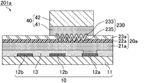
- a base film in which a printed circuit including a ground circuit is formed on a base film, an electromagnetic wave shield film including a shield layer and an insulating layer, and a metal foil are bent a plurality of times.
- a connecting member having a mountain fold portion formed in the above, a reinforcing member composed of a conductive adhesive layer and a metal reinforcing plate, and an insulating layer of the electromagnetic wave shielding film is formed on the shield layer of the electromagnetic wave shielding film.
- the electromagnetic wave shielding film is arranged on the base film so as to be located, the mountain fold portion of the connecting member penetrates the insulating layer of the electromagnetic wave shielding film, and the mountain folding portion of the connecting member is the electromagnetic wave.
- the connecting member is arranged on the electromagnetic wave shielding film so as to be in contact with the shield layer of the shield film, and the conductive adhesive of the reinforcing member is applied to the insulating layer of the electromagnetic wave shielding film and the metal foil of the connecting member.
- the reinforcing member is arranged on the electromagnetic wave shielding film and the connecting member so that the layers are in contact with each other, and the ground circuit of the base film and the metal reinforcing plate of the reinforcing member are electrically connected. It is characterized by being.
- a connecting member is used in order to electrically connect the ground circuit of the base film and the metal reinforcing plate of the reinforcing member. That is, in these shield-printed wiring boards of the present invention, the conductive filler, the conductive protrusion, or the mountain fold portion of the connecting member penetrates the insulating layer of the electromagnetic wave shielding film, and the conductive filler, the conductive protrusion, or the mountain of the connecting member. The folded portion is in contact with the shield layer of the electromagnetic wave shield film. Therefore, in the shield-printed wiring board of the present invention, the metal reinforcing plate of the reinforcing member and the shield layer of the electromagnetic wave shield film can be electrically connected via the connecting member. Therefore, in these shield-printed wiring boards of the present invention, the ground circuit of the substrate film and the metal reinforcing plate of the reinforcing member can be electrically connected via the connecting member.
- a conductive filler or the like is arranged on the conductive adhesive layer of the reinforcing member, and the metal of the reinforcing member is provided so that the conductive filler or the like penetrates the insulating layer of the electromagnetic wave shielding film.
- Pressure was applied to the reinforcing plate.
- the pressure may be dispersed and the conductive filler or the like may not sufficiently penetrate the insulating layer of the electromagnetic wave shielding film.
- the metal foil of the connecting member constituting the shield-printed wiring board of the present invention is more likely to apply pressure evenly than the metal reinforcing plate of the reinforcing member.
- the conductive filler, the conductive protrusion, or the mountain fold portion of the connecting member can easily penetrate the insulating layer of the electromagnetic wave shield film. Therefore, in the manufactured shield-printed wiring board of the present invention, the conductive filler, the conductive protrusion, or the mountain fold portion of the connecting member can be sufficiently brought into contact with the shield layer of the electromagnetic wave shield film. Therefore, the electric resistance value between the electromagnetic wave shield film and the connecting member can be lowered. As a result, in the shield-printed wiring board of the present invention, the ground circuit of the base film and the metal reinforcing plate of the reinforcing member are sufficiently electrically connected.
- the insulating layer of the electromagnetic wave shielding film has convex portions and / or concave portions, and the connecting member straddles the boundary between the convex portions and / or concave portions of the insulating layer of the electromagnetic wave shielding film. It may be arranged so as to.
- a conductive filler or the like is placed on the conductive adhesive layer of the reinforcing member, and pressure is applied to the reinforcing member so that the conductive filler or the like penetrates the insulating layer of the electromagnetic wave shielding film. Was there.
- the insulating layer of the electromagnetic wave shielding film is formed with recesses and / or protrusions caused by a printed circuit or the like provided on the substrate film, the pressure is easily dispersed, and a conductive filler or the like is formed. In some cases, it could not sufficiently penetrate the insulating layer of the electromagnetic wave shielding film.
- the metal foil of the connecting member constituting the shield-printed wiring board of the present invention is flexible and can be easily deformed. Therefore, even if the insulating layer of the electromagnetic wave shielding film has a concave portion and / or a convex portion, it can be deformed according to the shape.
- the conductive filler, the conductive protrusions, or the mountain folds of the connecting member can sufficiently penetrate the insulating layer of the electromagnetic wave shielding film. ..
- the electromagnetic wave shield film further includes a conductive adhesive layer
- the electromagnetic wave shield film includes a conductive adhesive layer of the electromagnetic wave shield film, a shield layer of the electromagnetic wave shield film, and ,
- the insulating layer of the electromagnetic wave shielding film is laminated in this order, the shielding layer of the electromagnetic wave shielding film is made of metal, and the conductive adhesive layer of the electromagnetic wave shielding film is in contact with the ground circuit of the substrate film. May be good.
- the electromagnetic wave shield film is laminated in the order of the shield layer of the electromagnetic wave shield film and the insulating layer of the electromagnetic wave shield film, and the shield layer of the electromagnetic wave shield film. Is made of a conductive adhesive, and the shield layer of the electromagnetic wave shielding film may be in contact with the ground circuit of the substrate film.
- the electromagnetic wave shield film further includes an insulating adhesive layer
- the electromagnetic wave shield film is an insulating adhesive layer of the electromagnetic wave shield film and a shield layer of the electromagnetic wave shield film.
- the insulating layer of the electromagnetic wave shielding film is laminated in this order, the shield layer of the electromagnetic wave shielding film is made of metal, and the surface of the shielding layer of the electromagnetic wave shielding film on the insulating adhesive layer side of the electromagnetic wave shielding film is The surface is roughened, and a part of the shield layer of the electromagnetic wave shield film may penetrate the insulating adhesive layer of the electromagnetic wave shield film and be in contact with the ground circuit of the base film.
- the structure of the electromagnetic wave shield film can function even if it has the above structure.
- the method for manufacturing a shielded printed wiring board of the present invention comprises a substrate film preparation step of preparing a substrate film in which a printed circuit including a ground circuit is formed on a base film, and an electromagnetic wave shielding film including a shield layer and an insulating layer.
- the electromagnetic wave shield film arranging step of laminating the base film so that the insulating layer of the electromagnetic wave shield film is located on the shield layer of the electromagnetic wave shield film, and the conductive filler is fixed to the metal foil by the adhesive resin.
- Reinforcing member arrangement in which the reinforcing member composed of the sex adhesive layer and the metal reinforcing plate is arranged so that the conductive adhesive layer of the reinforcing member comes into contact with the insulating layer of the electromagnetic wave shielding film and the metal foil of the connecting member. It is characterized by including a process.
- Another method for manufacturing a shield-printed wiring board of the present invention includes a base film preparation step of preparing a base film in which a printed circuit including a ground circuit is formed on a base film, and an electromagnetic wave shield film including a shield layer and an insulating layer.
- the electromagnetic wave shield film arranging step of laminating the base film so that the insulating layer of the electromagnetic wave shield film is located on the shield layer of the electromagnetic wave shield film, and the connecting member in which the conductive protrusions are formed on the metal foil.
- Another method for manufacturing a shielded printed wiring board of the present invention includes a substrate film preparation step of preparing a substrate film in which a printed circuit including a ground circuit is formed on a base film, and an electromagnetic wave shielding film including a shield layer and an insulating layer.
- the electromagnetic shielding film arranging step of laminating the base film so that the insulating layer of the electromagnetic shielding film is located on the shielding layer of the electromagnetic shielding film, and the pile formed by bending the metal foil a plurality of times.
- the connecting member having the fold portion is arranged on the electromagnetic wave shielding film so that the mountain fold portion of the connecting member penetrates the insulating layer of the electromagnetic wave shielding film and comes into contact with the shield layer of the electromagnetic wave shielding film.
- the process and the reinforcing member composed of the conductive adhesive layer and the metal reinforcing plate are arranged so that the conductive adhesive layer of the reinforcing member comes into contact with the insulating layer of the electromagnetic wave shielding film and the metal foil of the connecting member. It is characterized by including a reinforcing member arranging step.
- the conductive filler, the conductive protrusion, or the mountain fold portion of the connecting member penetrates the insulating layer of the electromagnetic wave shield film and comes into contact with the shield layer of the electromagnetic wave shield film. As shown above, it is arranged on the electromagnetic wave shield film. Therefore, in the manufactured shield printed wiring board, the electric resistance value between the electromagnetic wave shield film and the connecting member can be lowered. Therefore, according to the method for manufacturing a shield-printed wiring board of the present invention, it is possible to manufacture a shield-printed wiring board in which the ground circuit of the base film and the metal reinforcing plate of the reinforcing member are sufficiently electrically connected.
- the insulating layer of the electromagnetic wave shielding film has a convex portion and / or a concave portion
- the connecting member in the connecting member arranging step, is insulated from the electromagnetic wave shielding film. It may be arranged so as to straddle the boundary between the convex portion and / or the concave portion of the layer.
- the metal foil of the connecting member is flexible and can be easily deformed. Therefore, even if the insulating layer of the electromagnetic wave shielding film has a concave portion and / or a convex portion, it can be deformed according to the shape.
- the conductive filler, the conductive protrusions, or the mountain folds of the connecting member can sufficiently penetrate the insulating layer of the electromagnetic wave shielding film. ..
- the connecting member in which the conductive filler is fixed to the metal foil by the adhesive resin used in the method for manufacturing the shield printed wiring board of the present invention is the connecting member of the present invention.
- the connecting member in which the conductive protrusions are formed on the metal foil used in the method for manufacturing the shield printed wiring board of the present invention is the connecting member of the present invention.
- the connecting member having a mountain fold portion formed by bending the metal foil a plurality of times, which is used in the method for manufacturing the shield printed wiring board of the present invention is the connecting member of the present invention.
- the conductive filler, the conductive protrusion or the mountain fold portion of the connecting member penetrates the insulating layer of the electromagnetic wave shield film by the conductive filler, the conductive protrusion or the mountain fold portion of the connecting member, and the conductive filler, the conductive protrusion or the mountain fold portion of the connecting member is formed. It is in contact with the shield layer of the electromagnetic wave shield film. Therefore, in the shield-printed wiring board of the present invention, the metal reinforcing plate of the reinforcing member and the conductive filler, the conductive protrusion or the mountain fold portion of the connecting member are the conductive adhesive layer of the reinforcing member and the metal of the connecting member. It can be electrically connected via foil.
- the ground circuit of the substrate film and the metal reinforcing plate of the reinforcing member can be electrically connected via the connecting member.
- the metal foil of the connecting member constituting the shield-printed wiring board of the present invention can easily apply pressure evenly. Therefore, when the shield-printed wiring board of the present invention is manufactured, the conductive filler, the conductive protrusion, or the mountain fold portion of the connecting member can easily penetrate the insulating layer of the electromagnetic wave shield film. Therefore, in the manufactured shield-printed wiring board of the present invention, the conductive filler, the conductive protrusion, or the mountain fold portion of the connecting member can be sufficiently brought into contact with the shield layer of the electromagnetic wave shield film.
- the electric resistance value between the electromagnetic wave shield film and the connecting member can be lowered.
- the ground circuit of the base film and the metal reinforcing plate of the reinforcing member are sufficiently electrically connected.
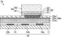
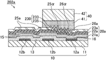
- FIG. 1 is a cross-sectional view schematically showing a cross-sectional view of a shield-printed wiring board according to a first embodiment of the present invention.
- FIG. 2 is a cross-sectional view schematically showing an example of a cross section of a shield printed wiring board in which a reinforcing member is arranged on an electromagnetic wave shield film having recesses and protrusions in an insulating layer without using a connecting member.
- FIG. 3 is a cross-sectional view schematically showing another example of the cross section of the shield printed wiring board according to the first embodiment of the present invention.
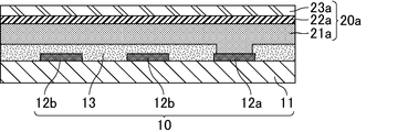
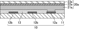
- FIG. 4 is a schematic view schematically showing an example of the substrate film preparation step according to the first embodiment of the present invention.
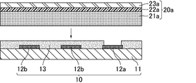
- FIG. 5A is a schematic view schematically showing an example of the electromagnetic wave shielding film arranging process according to the first embodiment of the present invention.
- FIG. 5B is a schematic view schematically showing an example of the electromagnetic wave shielding film arranging process according to the first embodiment of the present invention.
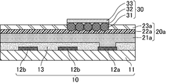
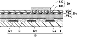
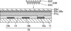
- FIG. 6A is a schematic view schematically showing an example of the connecting member arranging process according to the first embodiment of the present invention.
- FIG. 6B is a schematic view schematically showing an example of the connecting member arranging process according to the first embodiment of the present invention.
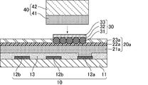
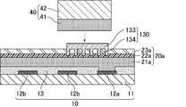
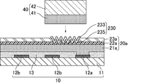
- FIG. 7A is a schematic view schematically showing an example of the reinforcing member arranging process according to the first embodiment of the present invention.
- FIG. 7B is a schematic view schematically showing an example of the reinforcing member arranging process according to the first embodiment of the present invention.
- FIG. 8 is a cross-sectional view schematically showing an example of a cross section of another shield printed wiring board according to the first embodiment of the present invention.
- FIG. 9 is a cross-sectional view schematically showing an example of a cross section of another shield printed wiring board according to the first embodiment of the present invention.
- FIG. 10 is a cross-sectional view schematically showing an example of a cross section of the shield printed wiring board according to the second embodiment of the present invention.
- FIG. 11 is a cross-sectional view schematically showing another example of the cross section of the shield printed wiring board according to the second embodiment of the present invention.
- FIG. 12 is a schematic view schematically showing an example of the substrate film preparation step according to the second embodiment of the present invention.
- FIG. 13A is a schematic view schematically showing an example of the electromagnetic wave shielding film arranging process according to the second embodiment of the present invention.
- FIG. 13B is a schematic view schematically showing an example of the electromagnetic wave shielding film arranging process according to the second embodiment of the present invention.
- FIG. 14A is a schematic view schematically showing an example of the connecting member arranging process according to the second embodiment of the present invention.
- FIG. 14B is a schematic view schematically showing an example of the connecting member arranging process according to the second embodiment of the present invention.
- FIG. 15A is a schematic view schematically showing an example of the reinforcing member arranging process according to the second embodiment of the present invention.
- FIG. 15B is a schematic view schematically showing an example of the reinforcing member arranging process according to the second embodiment of the present invention.
- FIG. 16 is a cross-sectional view schematically showing an example of a cross section of another shield printed wiring board according to the second embodiment of the present invention.
- FIG. 17 is a cross-sectional view schematically showing an example of a cross section of another shield-printed wiring board according to a second embodiment of the present invention.
- FIG. 18 is a cross-sectional view schematically showing an example of a cross section of the shield printed wiring board according to the third embodiment of the present invention.
- FIG. 19 is a cross-sectional view schematically showing another example of the cross section of the shield printed wiring board according to the third embodiment of the present invention.
- FIG. 16 is a cross-sectional view schematically showing an example of a cross section of another shield printed wiring board according to the second embodiment of the present invention.
- FIG. 17 is a cross-sectional view schematically showing an example of a cross section of
- FIG. 20 is a schematic view schematically showing an example of the substrate film preparation step according to the third embodiment of the present invention.
- FIG. 21A is a schematic view schematically showing an example of the electromagnetic wave shielding film arranging process according to the third embodiment of the present invention.
- FIG. 21B is a schematic view schematically showing an example of the electromagnetic wave shielding film arranging process according to the third embodiment of the present invention.
- FIG. 22A is a schematic view schematically showing an example of the connecting member arranging process according to the third embodiment of the present invention.
- FIG. 22B is a schematic view schematically showing an example of the connecting member arranging process according to the third embodiment of the present invention.
- FIG. 23A is a schematic view schematically showing an example of the reinforcing member arranging process according to the third embodiment of the present invention.
- FIG. 23B is a schematic view schematically showing an example of the reinforcing member arranging process according to the third embodiment of the present invention.
- FIG. 24 is a cross-sectional view schematically showing an example of a cross section of another shield-printed wiring board according to a third embodiment of the present invention.
- FIG. 25 is a cross-sectional view schematically showing an example of a cross section of another shield-printed wiring board according to a third embodiment of the present invention.
- the shield printed wiring board of the present invention will be specifically described.
- the present invention is not limited to the following embodiments, and can be appropriately modified and applied without changing the gist of the present invention.
- FIG. 1 is a cross-sectional view schematically showing an example of a cross section of a shielded printed wiring board according to a first embodiment of the present invention.
- the shield-printed wiring board 1a according to the first embodiment of the present invention is conductively adhered to a base film 10 on which a ground circuit 12a and other printed circuits 12b are formed on a base film 11.
- An electromagnetic wave shield film 20a in which an agent layer 21a, a shield layer 22a, and an insulating layer 23a are laminated in this order, a connecting member 30 in which a conductive filler 31 is fixed to a metal foil 33 by an adhesive resin 32, and a conductive adhesive layer 41.
- a reinforcing member 40 made of a metal reinforcing plate 42.
- the printed circuit 12b of the substrate film 10 is covered with the coverlay 13, and the ground circuit 12a of the substrate film 10 is not covered with the coverlay 13. Further, in the shield printed wiring board 1a, the electromagnetic wave shield film 20a is arranged on the base film 10 so that the conductive adhesive layer 21a of the electromagnetic wave shield film 20a comes into contact with the ground circuit 12a of the base film 10. In the shield printed wiring board 1a, since the printed circuit 12b of the base film 10 is covered with the coverlay 13, the printed circuit 12b and the conductive adhesive layer 21a of the electromagnetic wave shielding film 20a are not in contact with each other.
- the conductive filler 31 of the connecting member 30 penetrates the insulating layer 23a of the electromagnetic wave shielding film 20a, and the conductive filler 31 of the connecting member 30 comes into contact with the shield layer 22a of the electromagnetic wave shielding film 20a.
- the connecting member 30 is arranged on the electromagnetic wave shielding film 20a.
- the electromagnetic wave shield film 20a and the connecting member 30 are provided so that the conductive adhesive layer 41 of the reinforcing member 40 comes into contact with the insulating layer 23a of the electromagnetic wave shielding film 20a and the metal foil 33 of the connecting member 30.
- the reinforcing member 40 is arranged on the top.
- the ground circuit 12a of the base film 10 and the metal reinforcing plate 42 of the reinforcing member 40 are electrically connected.
- a connecting member 30 is used in order to electrically connect the ground circuit 12a of the base film 10 and the metal reinforcing plate 42 of the reinforcing member 40. That is, in the shield printed wiring board 1a, the conductive filler 31 of the connecting member 30 penetrates the insulating layer 23a of the electromagnetic wave shielding film 20a, and the conductive filler 31 of the connecting member 30 comes into contact with the shield layer 22a of the electromagnetic wave shielding film 20a. I'm letting you. Therefore, in the shield printed wiring board 1a, the metal reinforcing plate 42 of the reinforcing member 40 and the shield layer 22a of the electromagnetic wave shielding film 20a can be electrically connected to each other via the connecting member 30. Therefore, in the shield-printed wiring board 1a, the ground circuit 12a of the base film 10 and the metal reinforcing plate 42 of the reinforcing member 40 can be electrically connected via the connecting member 30.
- a conductive filler or the like is arranged on the conductive adhesive layer of the reinforcing member, and the metal of the reinforcing member is provided so that the conductive filler or the like penetrates the insulating layer of the electromagnetic wave shielding film.
- Pressure was applied to the reinforcing plate.
- the pressure may be dispersed and the conductive filler or the like may not sufficiently penetrate the insulating layer of the electromagnetic wave shielding film.
- the metal foil 33 of the connecting member 30 constituting the shield printed wiring board 1a is more likely to apply pressure evenly than the metal reinforcing plate 42 of the reinforcing member 40.
- the conductive filler 31 of the connecting member 30 can easily penetrate the insulating layer 23a of the electromagnetic wave shielding film 20a. Therefore, in the manufactured shield printed wiring board 1a, the conductive filler 31 of the connecting member 30 can be sufficiently brought into contact with the shield layer 22a of the electromagnetic wave shielding film 20a. Therefore, the electric resistance value between the electromagnetic wave shielding film 20a and the connecting member 30 can be lowered. As a result, in the shield printed wiring board 1a, the ground circuit 12a of the base film 10 and the metal reinforcing plate 42 of the reinforcing member 40 are sufficiently electrically connected.
- Electronic components will be mounted on the shield printed wiring board 1a.
- the reinforcing member 40 By arranging the reinforcing member 40 on the opposite side of the mounting portion of the electronic component, the mounting portion can be reinforced. Therefore, when the electronic component is mounted on the shield printed wiring board 1a, it is possible to prevent distortion or the like from occurring in the mounting portion.
- the insulating layer of the electromagnetic wave shielding film has a convex portion and / or a concave portion
- the connecting member is a convex portion and / or a convex portion of the insulating layer of the electromagnetic wave shielding film. It may be arranged so as to straddle the boundary of the recess.
- the shield-printed wiring board according to the first embodiment of the present invention in which the insulating layer of the electromagnetic wave shield film has a concave portion and / or a convex portion, first, a conventional shield-printed wiring board that does not use a connecting member is used. The board will be described.
- FIG. 2 is a cross-sectional view schematically showing an example of a cross section of a shield printed wiring board in which a reinforcing member is arranged on an electromagnetic wave shield film having recesses and protrusions in an insulating layer without using a connecting member.
- the conventional shield-printed wiring board 501 includes a base film 510 in which a ground circuit 512a and other printed circuits 512b are formed on a base film 511, a conductive adhesive layer 521, and a shield layer 522.
- the electromagnetic shielding film 520 in which the insulating layers 523 are laminated in this order, and the reinforcing member 540 composed of the conductive adhesive layer 541 containing the conductive filler 543 and the metal reinforcing plate 542 are provided.
- the printed circuit 512b of the substrate film 510 is covered with the coverlay 513, and the ground circuit 512a of the substrate film 510 is not covered with the coverlay 513.
- a convex portion 515 is formed on the coverlay 513 of the portion covering the print circuit 512b.
- a recess 516 is formed in the substrate film 510.
- the electromagnetic wave shield film 520 is arranged on the base film 510 so that the conductive adhesive layer 521 of the electromagnetic wave shield film 520 comes into contact with the ground circuit 512a.
- the concave portion 526 and the convex portion 525 are formed in the insulating layer 523 of the electromagnetic wave shield film 520 due to the concave portion 516 and the convex portion 515 of the base film 510.
- the insulating layer 523 of the electromagnetic wave shield film 520 is penetrated by the conductive filler 543 of the reinforcing member 540, and the conductive filler 543 of the reinforcing member 540 comes into contact with the shield layer 522 of the electromagnetic wave shield film 520.
- the reinforcing member 540 is arranged on the electromagnetic wave shielding film 520 so as to do so. Further, in the shield printed wiring board 501, the reinforcing member 540 is arranged so as to straddle the boundary 526 ⁇ of the concave portion 526 and the boundary 525 ⁇ of the convex portion 525 of the insulating layer 523 of the electromagnetic wave shielding film 520.
- the reinforcing member 540 When the shield printed wiring board 501 is manufactured, the reinforcing member 540 is pressed against the electromagnetic wave shielding film 520, so that the conductive filler 543 of the reinforcing member 540 penetrates the insulating layer 523 of the electromagnetic wave shielding film 520.
- the metal reinforcing plate 542 of the reinforcing member 540 is hard and hard to be deformed. Therefore, if the insulating layer 523 of the electromagnetic wave shielding film 520 has a concave portion 526 and a convex portion 525, it becomes difficult to apply uniform pressure to the entire conductive filler 543 of the reinforcing member 540. Therefore, as shown in FIG. 2, the shield printed wiring board 501 is provided with the conductive filler 543 of the reinforcing member 540 that does not sufficiently penetrate the insulating layer 523 of the electromagnetic wave shielding film 520.
- the conductive filler 543 of the reinforcing member 540 does not sufficiently penetrate the insulating layer 523 of the electromagnetic wave shielding film 520, the electrical resistance between the ground circuit 512a of the base film 510 and the metal reinforcing plate 542 of the reinforcing member 540. The value tends to be large.
- FIG. 3 is a cross-sectional view schematically showing another example of the cross section of the shield printed wiring board according to the first embodiment of the present invention.
- the shield-printed wiring board 2a is composed of a base film 10, an electromagnetic wave shield film 20a, a connecting member 30, and a reinforcing member 40, similarly to the shield-printed wiring board 1a.
- the printed circuit 12b of the substrate film 10 is covered with the coverlay 13, and the ground circuit 12a of the substrate film 10 is not covered with the coverlay 13.
- a convex portion 15 is formed on the coverlay 13 of the portion covering the print circuit 12b. Further, in the substrate film 10, since the ground circuit 12a is not covered with the coverlay 13, the recess 16 is formed.
- the electromagnetic wave shielding film 20a is arranged on the base film 10 so that the conductive adhesive layer 21a of the electromagnetic wave shielding film 20a comes into contact with the ground circuit 12a.
- the concave portion 26a and the convex portion 25a are formed in the insulating layer 23a of the electromagnetic wave shield film 20a due to the concave portion 16 and the convex portion 15 of the base film 10.
- the conductive filler 31 of the connecting member 30 penetrates the insulating layer 23a of the electromagnetic wave shielding film 20a so that the conductive filler 31 of the connecting member 30 comes into contact with the shield layer 22a of the electromagnetic wave shielding film 20a.
- the connecting member 30 is arranged on the electromagnetic wave shielding film 20a. Further, in the shield printed wiring board 2a, the connecting member 30 is arranged so as to straddle the boundary 26 ⁇ of the concave portion 26a and the boundary 25 ⁇ of the convex portion 25a of the insulating layer 23a of the electromagnetic wave shielding film 20a.
- the electromagnetic wave shield film 20a and the connecting member 30 are contacted with the conductive adhesive layer 41 of the reinforcing member 40 so that the insulating layer 23a of the electromagnetic wave shielding film 20a and the metal foil 33 of the connecting member 30 are in contact with each other.
- the reinforcing member 40 is arranged on the top.
- the metal foil 33 of the connecting member 30 is flexible and can be easily deformed. Therefore, even if the insulating layer 23a of the electromagnetic wave shielding film 20a has the concave portion 26a and the convex portion 25a, the metal foil 33 of the connecting member 30 can be deformed according to the shape. Therefore, even if the insulating layer 23a of the electromagnetic wave shielding film 20a has the concave portion 26a and the convex portion 25a, the conductive filler 31 of the connecting member 30 can sufficiently penetrate the insulating layer 23a of the electromagnetic wave shielding film 20a.
- the ground circuit 12a of the base film 10 and the metal reinforcing plate 42 of the reinforcing member 40 are sufficiently electrically connected.
- the materials of the base film 11 and the coverlay 13 constituting the base film 10 are not particularly limited, but are preferably made of engineering plastics.
- engineering plastics include resins such as polyethylene terephthalate, polypropylene, cross-linked polyethylene, polyester, polybenzimidazole, polyimide, polyimideamide, polyetherimide, and polyphenylene sulfide.
- a polyphenylene sulfide film is desirable when flame retardancy is required, and a polyimide film is desirable when heat resistance is required.
- the thickness of the base film 11 is preferably 10 to 40 ⁇ m.
- the thickness of the coverlay 13 is preferably 10 to 50 ⁇ m.
- the ground circuit 12a and the other printed circuits 12b constituting the substrate film 10 are not particularly limited, but can be formed by etching a conductive material or the like.
- Examples of the conductive material include known conductive materials such as copper, nickel, and gold.
- the thickness of the ground circuit 12a and the print circuit 12b is not particularly limited, but is appropriately set within the range of, for example, 10 to 100 ⁇ m.
- the conductive adhesive layer 21a may be made of any material as long as it has conductivity and can function as an adhesive.
- the conductive adhesive layer 21a may be composed of conductive particles and an adhesive resin composition.
- the conductive particles are not particularly limited, but may be metal fine particles, carbon nanotubes, carbon fibers, metal fibers, or the like.
- the metal fine particles are not particularly limited, but are silver powder, copper powder, nickel powder, solder powder, aluminum powder, silver-coated copper powder obtained by silver-plating copper powder, and polymer fine particles. Or glass beads or the like may be fine particles coated with metal. Among these, from the viewpoint of economy, it is desirable to use inexpensively available copper powder or silver-coated copper powder.
- the average particle size of the conductive particles is not particularly limited, but is preferably 0.5 to 15.0 ⁇ m. When the average particle diameter of the conductive particles is 0.5 ⁇ m or more, the conductivity of the conductive adhesive layer becomes good. When the average particle size of the conductive particles is 15.0 ⁇ m or less, the conductive adhesive layer can be thinned.
- the shape of the conductive particles is not particularly limited, but can be appropriately selected from spherical, flat, phosphorus flaky, dendrite-shaped, rod-shaped, fibrous, and the like.
- the material of the adhesive resin composition is not particularly limited, but is limited to a styrene resin composition, a vinyl acetate resin composition, a polyester resin composition, a polyethylene resin composition, a polypropylene resin composition, and an imide resin composition.
- Thermosetting resin compositions such as amide-based resin compositions and acrylic resin compositions, phenol-based resin compositions, epoxy-based resin compositions, urethane-based resin compositions, melamine-based resin compositions, and alkyd-based resin compositions.
- a thermosetting resin composition or the like can be used.
- the material of the adhesive resin composition may be one of these alone or in combination of two or more.
- the conductive adhesive layer 21a is provided with a curing accelerator, a tackifier, an antioxidant, a pigment, a dye, a plasticizer, an ultraviolet absorber, a defoaming agent, a leveling agent, a filler, and a flame retardant, if necessary. , A viscosity modifier and the like may be included.
- the blending amount of the conductive particles in the conductive adhesive layer 21a is not particularly limited, but is preferably 15 to 80% by mass, and more preferably 15 to 60% by mass. Within the above range, the adhesiveness is improved.
- the thickness of the conductive adhesive layer 21a is not particularly limited and can be appropriately set as needed, but it is preferably 0.5 to 20.0 ⁇ m. If the thickness of the conductive adhesive layer is less than 0.5 ⁇ m, it becomes difficult to obtain good conductivity. If the thickness of the conductive adhesive layer exceeds 20.0 ⁇ m, the thickness of the entire shield-printed wiring board becomes thick and difficult to handle.
- the conductive adhesive layer 21a has anisotropic conductivity.
- the transmission characteristics of the high frequency signal transmitted by the signal circuit of the printed wiring board are improved as compared with the case where the conductive adhesive layer 21a has anisotropic conductivity.
- the shield layer 22a is made of metal.
- the shield layer 22a may include a layer made of a material such as gold, silver, copper, aluminum, nickel, tin, palladium, chromium, titanium, zinc, etc., and preferably includes a copper layer. Copper is a suitable material for the shield layer 22a from the viewpoint of conductivity and economy.
- the shield layer 22a may include a layer made of the above metal alloy.
- the insulating layer 23a has sufficient insulating properties and is not particularly limited as long as it can protect the conductive adhesive layer 21a and the shielding layer 22a.
- a thermoplastic resin composition or a thermosetting resin composition It is desirable that it is composed of an active energy ray-curable composition or the like.
- the thermoplastic resin composition is not particularly limited, but is a styrene resin composition, a vinyl acetate resin composition, a polyester resin composition, a polyethylene resin composition, a polypropylene resin composition, and an imide resin composition. , Acrylic resin composition and the like.
- thermosetting resin composition is not particularly limited, and examples thereof include a phenol-based resin composition, an epoxy-based resin composition, a urethane-based resin composition, a melamine-based resin composition, and an alkyd-based resin composition.
- the active energy ray-curable composition is not particularly limited, and examples thereof include a polymerizable compound having at least two (meth) acryloyloxy groups in the molecule.
- the insulating layer 23a may be composed of one kind of single material, or may be made of two or more kinds of materials.
- the insulating layer 23a is provided with a curing accelerator, a tackifier, an antioxidant, a pigment, a dye, a plasticizer, an ultraviolet absorber, a defoaming agent, a leveling agent, a filler, a flame retardant, and a viscosity adjuster, if necessary. Agents, antiblocking agents and the like may be included.
- the thickness of the insulating layer 23a is not particularly limited and can be appropriately set as needed, but it is preferably 1 to 15 ⁇ m, and more preferably 3 to 10 ⁇ m. If the thickness of the insulating layer is less than 1 ⁇ m, it is too thin and it becomes difficult to sufficiently protect the conductive adhesive layer and the shield layer. If the thickness of the insulating layer exceeds 15 ⁇ m, the electromagnetic wave shielding film is difficult to bend because it is too thick, and the insulating layer itself is easily damaged. Therefore, it becomes difficult to apply it to a member that requires bending resistance.
- an anchor coat layer may be formed between the shielding layer 22a and the insulating layer 23a.
- the material of the anchor coat layer urethane resin, acrylic resin, core-shell type composite resin having urethane resin as shell and acrylic resin as core, epoxy resin, imide resin, amide resin, melamine resin, phenol resin, urea formaldehyde resin , Blocked isocyanate obtained by reacting polyisocyanate with a blocking agent such as phenol, polyvinyl alcohol, polyvinylpyrrolidone and the like.
- the conductive filler 31 is a group consisting of copper powder, silver powder, nickel powder, silver-coated copper powder, gold-coated copper powder, silver-coated nickel powder, gold-coated nickel powder, and particles obtained by coating resin with metal powder. It is desirable to include at least one selected from. These particles are excellent in conductivity.
- the average particle size of the conductive filler 31 is preferably 1 to 200 ⁇ m. If the average particle size of the conductive filler is less than 1 ⁇ m, the conductive filler is small and therefore difficult to penetrate the insulating layer of the electromagnetic wave shielding film. When the average particle size of the conductive filler exceeds 200 ⁇ m, the conductive filler becomes large, so that a large pressure is required to penetrate the insulating layer of the electromagnetic wave shielding film.
- the material of the adhesive resin 32 is not particularly limited, but is a styrene resin composition, a vinyl acetate resin composition, a polyester resin composition, a polyethylene resin composition, a polypropylene resin composition, and an imide.
- Thermoplastic resin compositions such as based resin compositions, amide based resin compositions, acrylic resin compositions, phenolic resin compositions, epoxy resin compositions, urethane resin compositions, melamine resin compositions, alkyds
- a thermosetting resin composition such as a based resin composition can be used.
- the material of the adhesive resin may be one of these alone or in combination of two or more.
- the metal leaf 33 is not particularly limited as long as it is made of a conductive metal, and is selected from the group consisting of, for example, copper, aluminum, silver, gold, platinum, nickel, chromium, titanium, zinc and stainless steel. It is desirable to include at least one of them. These materials have excellent conductivity.
- the thickness of the metal foil 33 is preferably 0.1 ⁇ m or more, and more preferably 1 ⁇ m or more. If the thickness of the metal foil is less than 0.1 ⁇ m, the strength of the metal foil is weakened and it is easily damaged.
- the thickness of the metal foil 33 of the connecting member 30 is equal to or less than the larger of the depth of the concave portion and the height of the convex portion. It is desirable that the thickness is 50% or less of the greater of the depth of the concave portion and the height of the convex portion.
- the thickness of the metal foil exceeds the height of the convex portion and / or the depth of the concave portion of the insulating layer of the electromagnetic wave shielding film, whichever is larger, the flexibility becomes low, and the concave portion of the insulating layer of the electromagnetic wave shielding film and the concave portion / Or it becomes difficult to deform according to the shape of the convex part.
- the conductive adhesive layer 41 may be made of any material as long as it has conductivity and can function as an adhesive.
- the conductive adhesive layer 41 may be composed of conductive particles and an adhesive resin composition.
- the conductive particles are not particularly limited, but may be metal fine particles, carbon nanotubes, carbon fibers, metal fibers, or the like.
- the metal fine particles are not particularly limited, but are silver powder, copper powder, nickel powder, solder powder, aluminum powder, silver-coated copper powder obtained by silver-plating copper powder, and polymer fine particles. Or glass beads or the like may be fine particles coated with metal. Among these, from the viewpoint of economy, it is desirable to use inexpensively available copper powder or silver-coated copper powder.
- the average particle size of the conductive particles is not particularly limited, but is preferably 0.5 to 15.0 ⁇ m. When the average particle diameter of the conductive particles is 0.5 ⁇ m or more, the conductivity of the conductive adhesive layer becomes good. When the average particle size of the conductive particles is 15.0 ⁇ m or less, the conductive adhesive layer can be thinned.
- the shape of the conductive particles is not particularly limited, but can be appropriately selected from spherical, flat, phosphorus flaky, dendrite-shaped, rod-shaped, fibrous, and the like.
- the material of the adhesive resin composition is not particularly limited, but is limited to a styrene resin composition, a vinyl acetate resin composition, a polyester resin composition, a polyethylene resin composition, a polypropylene resin composition, and an imide resin composition.
- Thermosetting resin compositions such as amide-based resin compositions and acrylic resin compositions, phenol-based resin compositions, epoxy-based resin compositions, urethane-based resin compositions, melamine-based resin compositions, and alkyd-based resin compositions.
- a thermosetting resin composition or the like can be used.
- the material of the adhesive resin composition may be one of these alone or in combination of two or more.
- the conductive adhesive layer 41 may contain, if necessary, a curing accelerator, a tackifier, an antioxidant, a pigment, a dye, a plasticizer, an ultraviolet absorber, a defoamer, a leveling agent, a filler, and a flame retardant. , A viscosity modifier and the like may be included.
- the blending amount of the conductive particles in the conductive adhesive layer 41 is not particularly limited, but is preferably 15 to 80% by mass, and more preferably 15 to 60% by mass. Within the above range, the adhesiveness is improved.
- the thickness of the conductive adhesive layer 41 is not particularly limited and can be appropriately set as needed, but it is preferably 0.5 to 80.0 ⁇ m. If the thickness of the conductive adhesive layer is less than 0.5 ⁇ m, it becomes difficult to obtain good conductivity. If the thickness of the conductive adhesive layer exceeds 80.0 ⁇ m, the thickness of the entire reinforcing member becomes thick and difficult to handle.
- the metal reinforcing plate 42 is made of a conductive metal material, and when an electronic component is mounted on the shield-printed wiring board 1a, distortion or the like caused at the mounting portion due to bending or the like is generated. Any metal material can be used as long as it can be prevented. Examples of such metal materials include copper, aluminum, silver, gold, platinum, nickel, chromium, titanium, zinc, stainless steel, and alloys thereof.
- the thickness of the metal reinforcing plate 42 is preferably 0.05 mm to 1 mm. If the thickness of the metal reinforcing plate is less than 0.05 mm, the strength is not sufficient, and distortion or the like is likely to occur when mounting electronic components on the shield-printed wiring board. If the thickness of the metal reinforcing plate exceeds 1 mm, it becomes bulky, and it becomes difficult to arrange the shield printed wiring board in the electronic device.
- the method for manufacturing the shield printed wiring board is also an example of the method for manufacturing the shield printed wiring board according to the first embodiment of the present invention.
- the method for manufacturing the shield printed wiring board 1a includes (1) a substrate film preparation step, (2) an electromagnetic wave shield film placement step, (3) a connection member placement step, and (4) a reinforcement member placement step. May be good.
- FIG. 4 is a schematic view schematically showing an example of the substrate film preparation step according to the first embodiment of the present invention.
- 5A and 5B are schematic views schematically showing an example of an electromagnetic wave shielding film arranging process according to the first embodiment of the present invention.
- 6A and 6B are schematic views schematically showing an example of a connecting member arranging process according to the first embodiment of the present invention.
- 7A and 7B are schematic views schematically showing an example of a reinforcing member arranging process according to the first embodiment of the present invention.
- an electromagnetic wave shield film 20a in which the conductive adhesive layer 21a, the shield layer 22a, and the insulating layer 23a are laminated in this order is prepared.
- the electromagnetic wave shielding film 20a is laminated on the base film 10 so that the conductive adhesive layer 21a of the electromagnetic wave shielding film 20a comes into contact with the ground circuit 12a of the base film 10.
- connection member placement step Next, as shown in FIG. 6A, the conductive filler 31 is fixed to the metal foil 33 with the adhesive resin 32 so that a part of the conductive filler 31 is exposed, and the conductive filler 31 is conductive.
- a connecting member 30 in which the sex filler 31 is fixed to the metal foil 33 by the adhesive resin 32 is prepared.
- the connecting member 30 is electromagnetically shielded so that the conductive filler 31 of the connecting member 30 penetrates the insulating layer 23a of the electromagnetic wave shielding film 20a and comes into contact with the shield layer 22a of the electromagnetic wave shielding film 20a.
- the connecting member 30 is arranged on the electromagnetic wave shielding film 20a.
- a reinforcing member 40 composed of the conductive adhesive layer 41 and the metal reinforcing plate 42 is prepared.
- the reinforcing member 40 is arranged so that the conductive adhesive layer 41 of the reinforcing member 40 comes into contact with the insulating layer 23a of the electromagnetic wave shielding film 20a and the metal foil 33 of the connecting member 30.
- the shield printed wiring board 1a can be manufactured.
- the insulating layer 23a of the electromagnetic wave shielding film 20a has no concave portion and / or convex portion.
- the insulating layer of the electromagnetic wave shield film has a convex portion and / or a concave portion, and in the connection member arranging step, the connection member is used. It may be arranged so as to straddle the boundary between the convex portion and / or the concave portion of the insulating layer of the electromagnetic wave shielding film.
- the metal foil of the connecting member is flexible and can be easily deformed.
- the conductive filler of the connecting member can sufficiently penetrate the insulating layer of the electromagnetic wave shielding film.
- the connecting member 30 used in the method for manufacturing the shield printed wiring board 1a is also the connecting member of the present invention.
- the conductive filler 31 was fixed to the metal foil 33 by the adhesive resin 32 so that a part of the conductive filler 31 was exposed, but the connecting member of the present invention has adhesiveness.
- the conductive filler may be fixed to the metal foil so that the resin covers the entire conductive filler.
- FIG. 8 is a cross-sectional view schematically showing an example of a cross section of another shield printed wiring board according to the first embodiment of the present invention.
- Another shield-printed wiring board 1b according to the first embodiment of the present invention is an electromagnetic wave in which the electromagnetic wave shield film 20a of the shield-printed wiring board 1a is laminated with a shield layer 22b and an insulating layer 23b made of a conductive adhesive in this order. It has the same configuration as the shield printed wiring board 1a except that it is replaced with the shield film 20b.
- the shield printed wiring board 1b includes a base film 10 on which a ground circuit 12a and other printed circuits 12b are formed on a base film 11, a shield layer 22b made of a conductive adhesive, and the like. It is composed of an electromagnetic wave shielding film 20b in which an insulating layer 23b is laminated in order, a connecting member 30 in which a conductive filler 31 is fixed to a metal foil 33 by an adhesive resin 32, a conductive adhesive layer 41, and a metal reinforcing plate 42. A reinforcing member 40 is provided.
- the printed circuit 12b of the substrate film 10 is covered with the coverlay 13, and the ground circuit 12a of the substrate film 10 is not covered with the coverlay 13. Further, in the shield printed wiring board 1b, the electromagnetic wave shield film 20b is arranged on the base film 10 so that the shield layer 22b of the electromagnetic wave shield film 20b comes into contact with the ground circuit 12a of the base film 10. In the shield print wiring board 1b, since the print circuit 12b of the base film 10 is covered with the coverlay 13, the print circuit 12b and the shield layer 22b of the electromagnetic wave shield film 20b are not in contact with each other.
- the conductive filler 31 of the connecting member 30 penetrates the insulating layer 23b of the electromagnetic wave shielding film 20b, and the conductive filler 31 of the connecting member 30 comes into contact with the shield layer 22b of the electromagnetic wave shielding film 20b.
- the connecting member 30 is arranged on the electromagnetic wave shielding film 20b.
- the electromagnetic wave shield film 20b and the connecting member 30 are provided so that the conductive adhesive layer 41 of the reinforcing member 40 comes into contact with the insulating layer 23b of the electromagnetic wave shielding film 20b and the metal foil 33 of the connecting member 30.
- the reinforcing member 40 is arranged on the top.
- the ground circuit 12a of the base film 10 and the metal reinforcing plate 42 of the reinforcing member 40 are electrically connected.
- the shield-printed wiring board 1b has the same effect as the shield-printed wiring board 1a, although the structure of the electromagnetic wave shield film is different.
- the shield layer 22b may be made of any material as long as it is made of a conductive adhesive and has an electromagnetic wave shielding function.
- the shield layer 22b may be composed of conductive particles and an adhesive resin composition.
- the conductive particles are not particularly limited, but may be metal fine particles, carbon nanotubes, carbon fibers, metal fibers, or the like.
- the metal fine particles are not particularly limited, but are silver powder, copper powder, nickel powder, solder powder, aluminum powder, silver-coated copper powder obtained by silver-plating copper powder, and polymer fine particles. Or glass beads or the like may be fine particles coated with metal. Among these, from the viewpoint of economy, it is desirable to use inexpensively available copper powder or silver-coated copper powder.
- the average particle size of the conductive particles is not particularly limited, but is preferably 0.5 to 15.0 ⁇ m. When the average particle diameter of the conductive particles is 0.5 ⁇ m or more, the conductivity of the conductive adhesive layer becomes good. When the average particle size of the conductive particles is 15.0 ⁇ m or less, the conductive adhesive layer can be thinned.
- the shape of the conductive particles is not particularly limited, but can be appropriately selected from spherical, flat, phosphorus flaky, dendrite-shaped, rod-shaped, fibrous, and the like.
- the material of the adhesive resin composition is not particularly limited, but is limited to a styrene resin composition, a vinyl acetate resin composition, a polyester resin composition, a polyethylene resin composition, a polypropylene resin composition, and an imide resin composition.
- Thermosetting resin compositions such as amide-based resin compositions and acrylic resin compositions, phenol-based resin compositions, epoxy-based resin compositions, urethane-based resin compositions, melamine-based resin compositions, and alkyd-based resin compositions.
- a thermosetting resin composition or the like can be used.
- the material of the adhesive resin composition may be one of these alone or in combination of two or more.
- the shield layer 22b is provided with a curing accelerator, a tackifier, an antioxidant, a pigment, a dye, a plasticizer, an ultraviolet absorber, an antifoaming agent, a leveling agent, a filler, a flame retardant, and a viscosity adjuster, if necessary. Agents and the like may be included.
- the blending amount of the conductive particles in the shield layer 22b is not particularly limited, but is preferably 15 to 80% by mass, and more preferably 15 to 60% by mass. Within the above range, the adhesiveness is improved.
- the insulating layer 23b has sufficient insulating properties and is not particularly limited as long as the shield layer 22b can be protected.
- a thermoplastic resin composition for example, a thermoplastic resin composition, a thermosetting resin composition, or an active energy ray-curable composition. It is desirable that it is composed of things.
- the thermoplastic resin composition is not particularly limited, but is a styrene resin composition, a vinyl acetate resin composition, a polyester resin composition, a polyethylene resin composition, a polypropylene resin composition, and an imide resin composition. , Acrylic resin composition and the like.
- thermosetting resin composition is not particularly limited, and examples thereof include a phenol-based resin composition, an epoxy-based resin composition, a urethane-based resin composition, a melamine-based resin composition, and an alkyd-based resin composition.
- the active energy ray-curable composition is not particularly limited, and examples thereof include a polymerizable compound having at least two (meth) acryloyloxy groups in the molecule.
- the insulating layer 23b may be composed of one kind of single material, or may be made of two or more kinds of materials.
- the insulating layer 23b is provided with a curing accelerator, a tackifier, an antioxidant, a pigment, a dye, a plasticizer, an ultraviolet absorber, a defoaming agent, a leveling agent, a filler, a flame retardant, and a viscosity adjuster, if necessary. Agents, antiblocking agents and the like may be included.
- the thickness of the insulating layer 23b is not particularly limited and can be appropriately set as needed, but it is preferably 1 to 15 ⁇ m, and more preferably 3 to 10 ⁇ m. If the thickness of the insulating layer is less than 1 ⁇ m, it is too thin and it becomes difficult to sufficiently protect the conductive adhesive layer and the shield layer. If the thickness of the insulating layer exceeds 15 ⁇ m, the electromagnetic wave shielding film is difficult to bend because it is too thick, and the insulating layer itself is easily damaged. Therefore, it becomes difficult to apply it to a member that requires bending resistance.
- an anchor coat layer may be formed between the shield layer 22b and the insulating layer 23b.
- the material of the anchor coat layer urethane resin, acrylic resin, core-shell type composite resin having urethane resin as shell and acrylic resin as core, epoxy resin, imide resin, amide resin, melamine resin, phenol resin, urea formaldehyde resin , Blocked isocyanate obtained by reacting polyisocyanate with a blocking agent such as phenol, polyvinyl alcohol, polyvinylpyrrolidone and the like.
- the desirable configurations and materials of the base film 10 and the reinforcing member 40 in the shield printed wiring board 1b are the same as the desirable configurations and materials of the substrate film 10 and the reinforcing member 40 in the shield printed wiring board 1a.
- a shield layer made of a conductive adhesive instead of the electromagnetic wave shield film 20a.
- An electromagnetic wave shielding film 20b in which 22b and an insulating layer 23b are laminated in this order may be used.
- the insulating layer 23b of the electromagnetic wave shield film 20b is formed with recesses and protrusions due to the print circuit 12b and the ground circuit 12a.
- the shield print of the present invention is provided.
- the insulating layer of the electromagnetic wave shielding film is not formed with recesses and protrusions, and may be flat.
- FIG. 9 is a cross-sectional view schematically showing an example of a cross section of another shield printed wiring board according to the first embodiment of the present invention.
- the electromagnetic wave shield film 20a of the shield-printed wiring board 1a is laminated with an insulating adhesive layer 24c, a shield layer 22c made of metal, and an insulating layer 23c in this order. It has the same configuration as the shield printed wiring board 1a except that it is replaced with the electromagnetic wave shield film 20c.
- the shield printed wiring board 1c is a shield made of a base film 10 in which a ground circuit 12a and other printed circuits 12b are formed on a base film 11, an insulating adhesive layer 24c, and a metal.
- the surface 27c of the shield layer 22c on the insulating adhesive layer 24c side is roughened, and a concave portion 28c and a convex portion 29c are formed.
- the printed circuit 12b of the substrate film 10 is covered with the coverlay 13, and the ground circuit 12a of the substrate film 10 is not covered with the coverlay 13. Further, in the shield printed wiring board 1c, an electromagnetic wave is applied on the base film 10 so that the convex portion 29c, which is a part of the shield layer 22c, penetrates the insulating adhesive layer 24c and contacts the ground circuit 12a of the base film 10.
- the shield film 20c is arranged.
- the print circuit 12b of the base film 10 is covered with the coverlay 13
- the print circuit 12b and the shield layer 22c of the electromagnetic wave shield film 20c are not in contact with each other.
- the conductive filler 31 of the connecting member 30 penetrates the insulating layer 23c of the electromagnetic wave shielding film 20c, and the conductive filler 31 of the connecting member 30 comes into contact with the shield layer 22c of the electromagnetic wave shielding film 20c.
- the connecting member 30 is arranged on the electromagnetic wave shielding film 20c.
- the electromagnetic wave shield film 20c and the connecting member 30 are provided so that the conductive adhesive layer 41 of the reinforcing member 40 comes into contact with the insulating layer 23c of the electromagnetic wave shielding film 20c and the metal foil 33 of the connecting member 30.
- the reinforcing member 40 is arranged on the top.
- the ground circuit 12a of the base film 10 and the metal reinforcing plate 42 of the reinforcing member 40 are electrically connected.
- the shield-printed wiring board 1c has a different structure of the electromagnetic wave shield film, it has the same effect as the shield-printed wiring board 1a.
- the material of the insulating adhesive layer 24c is not particularly limited, but is a styrene resin composition, a vinyl acetate resin composition, a polyester resin composition, a polyethylene resin composition, and a polypropylene resin composition. , Imid resin composition, amide resin composition, acrylic resin composition and other thermoplastic resin compositions, phenol resin composition, epoxy resin composition, urethane resin composition, melamine resin composition. , A thermocurable resin composition such as an alkyd resin composition can be used.
- the material of the insulating adhesive layer 24c may be one of these alone or in combination of two or more.
- the insulating adhesive layer 24c contains, if necessary, a curing accelerator, a tackifier, an antioxidant, a pigment, a dye, a plasticizer, an ultraviolet absorber, a defoamer, a leveling agent, a filler, a flame retardant, and the like.
- a viscosity modifier or the like may be contained.
- the thickness of the insulating adhesive layer 24c is not particularly limited, but is preferably 0.5 to 20.0 ⁇ m, and more preferably 1 to 15 ⁇ m. If the thickness of the insulating adhesive layer is less than 0.5 ⁇ m, the strength of the insulating adhesive layer is weak and it is easily damaged. If the thickness of the insulating adhesive layer exceeds 20.0 ⁇ m, it becomes difficult for the shield layer to penetrate the insulating adhesive layer.
- the shield layer 22c is made of metal.
- the shield layer 22c may include a layer made of a material such as gold, silver, copper, aluminum, nickel, tin, palladium, chromium, titanium, zinc, etc., and preferably includes a copper layer. Copper is a suitable material for the shield layer 22c from the viewpoint of conductivity and economy.
- the shield layer 22c may include a layer made of the above metal alloy.
- the surface 27c of the shield layer 22c on the insulating adhesive layer 24c side is roughened, but the surface roughness Ra is preferably 0.5 to 30 ⁇ m, and 0.5 to 0.5 to It is preferably 20 ⁇ m.
- the surface roughness Ra is less than 0.5 ⁇ m, it becomes difficult for the convex portion of the shield layer to penetrate the insulating adhesive layer.
- the surface roughness Ra exceeds 30 ⁇ m, the shield layer is rougher than necessary, and the cost of forming such a shield layer is high.
- the insulating layer 23c has sufficient insulating properties and is not particularly limited as long as it can protect the insulating adhesive layer 24c and the shielding layer 22c.
- a thermoplastic resin composition for example, a thermoplastic resin composition, a thermosetting resin composition, and the like. It is desirable that it is composed of an active energy ray-curable composition or the like.
- the thermoplastic resin composition is not particularly limited, but is a styrene resin composition, a vinyl acetate resin composition, a polyester resin composition, a polyethylene resin composition, a polypropylene resin composition, and an imide resin composition. , Acrylic resin composition and the like.
- thermosetting resin composition is not particularly limited, and examples thereof include a phenol-based resin composition, an epoxy-based resin composition, a urethane-based resin composition, a melamine-based resin composition, and an alkyd-based resin composition.
- the active energy ray-curable composition is not particularly limited, and examples thereof include a polymerizable compound having at least two (meth) acryloyloxy groups in the molecule.
- the insulating layer 23c may be composed of one kind of single material, or may be made of two or more kinds of materials.
- the insulating layer 23c is provided with a curing accelerator, a tackifier, an antioxidant, a pigment, a dye, a plasticizer, an ultraviolet absorber, a defoaming agent, a leveling agent, a filler, a flame retardant, and a viscosity adjuster, if necessary. Agents, antiblocking agents and the like may be included.
- the thickness of the insulating layer 23c is not particularly limited and can be appropriately set as needed, but it is preferably 1 to 15 ⁇ m, and more preferably 3 to 10 ⁇ m. If the thickness of the insulating layer is less than 1 ⁇ m, it is too thin and it becomes difficult to sufficiently protect the conductive adhesive layer and the shield layer. If the thickness of the insulating layer exceeds 15 ⁇ m, the electromagnetic wave shielding film is difficult to bend because it is too thick, and the insulating layer itself is easily damaged. Therefore, it becomes difficult to apply it to a member that requires bending resistance.
- an anchor coat layer may be formed between the shielding layer 22c and the insulating layer 23c.
- the material of the anchor coat layer urethane resin, acrylic resin, core-shell type composite resin having urethane resin as shell and acrylic resin as core, epoxy resin, imide resin, amide resin, melamine resin, phenol resin, urea formaldehyde resin , Blocked isocyanate obtained by reacting polyisocyanate with a blocking agent such as phenol, polyvinyl alcohol, polyvinylpyrrolidone and the like.
- the desirable configurations and materials of the base film 10 and the reinforcing member 40 in the shield printed wiring board 1c are the same as the desirable configurations and materials of the substrate film 10 and the reinforcing member 40 in the shield printed wiring board 1a.
- the shield printed wiring board 1c As a method of manufacturing the shield printed wiring board 1c, in the (2) electromagnetic wave shield film arranging step of the method of manufacturing the shield printed wiring board 1a, instead of the electromagnetic wave shield film 20a, the insulating adhesive layer 24c and metal are used. An electromagnetic wave shielding film 20c in which the shielding layer 22c and the insulating layer 23c are laminated in this order may be used. When preparing the electromagnetic wave shield film 20c, the convex portion 29c of the shield layer 22c does not have to penetrate the insulating adhesive layer 24c.
- the insulating layer 23b of the electromagnetic wave shield film 20c is formed with recesses and protrusions due to the print circuit 12b and the ground circuit 12a, but the shield print of the present invention is formed.
- the insulating layer of the electromagnetic wave shielding film is not formed with recesses and protrusions, and may be flat.
- FIG. 10 is a cross-sectional view schematically showing an example of a cross section of the shield printed wiring board according to the second embodiment of the present invention.
- the connecting member 30 of the shield-printed wiring board 1a is replaced with the connecting member 130 in which the conductive protrusion 134 is formed on the metal foil 133. It has the same configuration as the shield printed wiring board 1a.
- the shield printed wiring board 101a includes a base film 10 in which a ground circuit 12a and other printed circuits 12b are formed on a base film 11, a conductive adhesive layer 21a, and a shield layer 22a.
- a base film 10 in which a ground circuit 12a and other printed circuits 12b are formed on a base film 11, a conductive adhesive layer 21a, and a shield layer 22a.
- An electromagnetic wave shielding film 20a in which an insulating layer 23a is laminated in this order, a connecting member 130 in which a conductive projection 134 is formed on a metal foil 133, and a reinforcing member 40 composed of a conductive adhesive layer 41 and a metal reinforcing
- the electromagnetic wave shield film 20a is provided so that the conductive protrusion 134 of the connecting member 130 penetrates the insulating layer 23a of the electromagnetic wave shield film 20a and comes into contact with the shield layer 22a of the electromagnetic wave shield film 20a.
- the connecting member 130 is arranged on the top.
- the electromagnetic wave shield film 20a and the connecting member 130 are provided so that the conductive adhesive layer 41 of the reinforcing member 40 comes into contact with the insulating layer 23a of the electromagnetic wave shielding film 20a and the metal foil 133 of the connecting member 130.
- the reinforcing member 40 is arranged on the top.
- the connecting member 130 in the shield printed wiring board 101a, the conductive projection 134 of the connecting member 130 can be sufficiently brought into contact with the shield layer 22a of the electromagnetic wave shielding film 20a. Therefore, the electric resistance value between the electromagnetic wave shielding film 20a and the connecting member 130 can be lowered. As a result, in the shield printed wiring board 101a, the ground circuit 12a of the base film 10 and the metal reinforcing plate 42 of the reinforcing member 40 are sufficiently electrically connected.
- the insulating layer of the electromagnetic wave shielding film has a convex portion and / or a concave portion
- the connecting member is a convex portion and / or a convex portion of the insulating layer of the electromagnetic wave shielding film. It may be arranged so as to straddle the boundary of the recess.
- FIG. 11 is a cross-sectional view schematically showing another example of the cross section of the shield printed wiring board according to the second embodiment of the present invention.
- the shield-printed wiring board 102a is composed of a base film 10, an electromagnetic wave shield film 20a, a connecting member 130, and a reinforcing member 40, similarly to the shield-printed wiring board 101a.
- the printed circuit 12b of the substrate film 10 is covered with the coverlay 13, and the ground circuit 12a of the substrate film 10 is not covered with the coverlay 13.
- a convex portion 15 is formed on the coverlay 13 of the portion covering the print circuit 12b. Further, in the substrate film 10, since the ground circuit 12a is not covered with the coverlay 13, the recess 16 is formed.
- the electromagnetic wave shielding film 20a is arranged on the base film 10 so that the conductive adhesive layer 21a of the electromagnetic wave shielding film 20a comes into contact with the ground circuit 12a.
- the concave portion 26a and the convex portion 25a are formed in the insulating layer 23a of the electromagnetic wave shield film 20a due to the concave portion 16 and the convex portion 15 of the base film 10.
- the conductive projection 134 of the connecting member 130 penetrates the insulating layer 23a of the electromagnetic wave shielding film 20a, and the conductive projection 134 of the connecting member 130 contacts the shield layer 22a of the electromagnetic wave shielding film 20a.
- the connecting member 130 is arranged on the electromagnetic wave shielding film 20a so as to do so. Further, in the shield printed wiring board 102a, the connecting member 130 is arranged so as to straddle the boundary 26 ⁇ of the concave portion 26a and the boundary 25 ⁇ of the convex portion 25a of the insulating layer 23a of the electromagnetic wave shielding film 20a.
- the electromagnetic wave shield film 20a and the connecting member 130 are contacted so that the conductive adhesive layer 41 of the reinforcing member 40 comes into contact with the insulating layer 23a of the electromagnetic wave shielding film 20a and the metal foil 133 of the connecting member 130.
- the reinforcing member 40 is arranged on the top.
- the metal foil 133 of the connecting member 130 is flexible and can be easily deformed. Therefore, even if the insulating layer 23a of the electromagnetic wave shielding film 20a has the concave portion 26a and the convex portion 25a, the metal foil 133 of the connecting member 130 can be deformed according to the shape. Therefore, even if the insulating layer 23a of the electromagnetic wave shielding film 20a has the concave portion 26a and the convex portion 25a, the conductive projection 134 of the connecting member 130 can sufficiently penetrate the insulating layer 23a of the electromagnetic wave shielding film 20a.
- the ground circuit 12a of the base film 10 and the metal reinforcing plate 42 of the reinforcing member 40 are sufficiently electrically connected.
- the conductive protrusion 134 may be integrated with the metal foil 133, or may be adhered to the metal foil 133 with an adhesive resin.
- the metal leaf 133 is not particularly limited as long as it is made of a conductive metal, for example, at least selected from the group consisting of copper, aluminum, silver, gold, nickel, chromium, titanium, zinc and stainless steel. It is desirable to include one type. These materials have excellent conductivity.
- the thickness of the metal foil 133 is preferably 0.1 ⁇ m or more, and more preferably 1 ⁇ m or more. If the thickness of the metal foil is less than 0.1 ⁇ m, the strength of the metal foil is weakened and it is easily damaged.
- the thickness of the metal foil 133 of the connecting member 130 is equal to or less than the larger of the depth of the concave portion and the height of the convex portion. It is desirable that the thickness is 50% or less of the greater of the depth of the concave portion and the height of the convex portion. If the thickness of the metal foil exceeds the height of the convex portion and / or the depth of the concave portion of the insulating layer of the electromagnetic wave shielding film, whichever is greater, the flexibility becomes low, and the concave portion and the concave portion of the insulating layer of the electromagnetic wave shielding film are formed. / Or it becomes difficult to deform according to the shape of the convex part.
- the material of the conductive projection 134 is not particularly limited and includes, for example, at least one selected from the group consisting of copper, aluminum, silver, gold, nickel, chromium, titanium, zinc and stainless steel. Is desirable. Further, it is desirable that the metal foil 133 and the conductive protrusion 134 are made of the same material.
- the conductive protrusion 134 may be a cylinder, for example, a cylinder, an elliptical prism, a triangular prism, a quadrangular prism, a pentagonal prism, a hexagonal prism, an octagonal prism, or the like.
- the conductive projection 134 When the conductive projection 134 is columnar, it easily penetrates the insulating layer 23a of the electromagnetic wave shielding film 20a.
- the area of the bottom surface of the conductive protrusions 134 is desirably 1.0 ⁇ 1.0 ⁇ 10 6 ⁇ m 2 . If the area of the bottom surface of the conductive protrusion is less than 1.0 ⁇ m 2 , the strength of the conductive protrusion is weakened, and the conductive protrusion is easily broken. When the area of the bottom surface of the conductive protrusions is more than 1.0 ⁇ 10 6 ⁇ m 2, since the conductive protrusions is too thick, hardly penetrate the insulating layer of the electromagnetic wave shielding film.
- the pitch between the conductive projections 134 is preferably 1 to 1000 ⁇ m. It is technically difficult to manufacture a connecting member in which the pitch between the conductive protrusions is less than 1 ⁇ m. When the pitch between the conductive protrusions exceeds 1000 ⁇ m, the density becomes low, and the total contact area between the conductive protrusions of the connecting member and the shield layer of the electromagnetic wave shielding film becomes small. Therefore, the electrical resistance tends to be high.
- the height of the conductive projection 134 is not particularly limited as long as it can penetrate the insulating layer 23a of the electromagnetic wave shielding film 20a, but it is preferably 1 to 60 ⁇ m.
- the desirable configurations and materials of the base film 10, the electromagnetic wave shield film 20a, and the reinforcing member 40 of the shield printed wiring board 101a are the desirable configurations and materials of the base film 10, the electromagnetic wave shielding film 20a, and the reinforcing member 40 of the shield printed wiring board 1a. And so on.
- the method for manufacturing the shield printed wiring board is also an example of the method for manufacturing the shield printed wiring board according to the second embodiment of the present invention.
- the method for manufacturing the shield printed wiring board 101a includes (1) a substrate film preparation step, (2) an electromagnetic wave shield film placement step, (3) a connection member placement step, and (4) a reinforcement member placement step. May be good.
- FIG. 12 is a schematic view schematically showing an example of the substrate film preparation step according to the second embodiment of the present invention.
- 13A and 13B are schematic views schematically showing an example of an electromagnetic wave shielding film arranging process according to a second embodiment of the present invention.
- 14A and 14B are schematic views schematically showing an example of a connecting member arranging process according to a second embodiment of the present invention.
- 15A and 15B are schematic views schematically showing an example of a reinforcing member arranging process according to a second embodiment of the present invention.
- an electromagnetic wave shield film 20a in which the conductive adhesive layer 21a, the shield layer 22a, and the insulating layer 23a are laminated in this order is prepared.
- the electromagnetic wave shielding film 20a is laminated on the base film 10 so that the conductive adhesive layer 21a of the electromagnetic wave shielding film 20a comes into contact with the ground circuit 12a of the base film 10.
- connection member 130 in which the conductive protrusions 134 are formed on the metal foil 133 is prepared.
- the connecting member 130 is electromagnetically shielded so that the conductive protrusion 134 of the connecting member 130 penetrates the insulating layer 23a of the electromagnetic wave shielding film 20a and comes into contact with the shield layer 22a of the electromagnetic wave shielding film 20a.
- the connecting member 130 is arranged on the electromagnetic wave shielding film 20a.
- a reinforcing member 40 composed of the conductive adhesive layer 41 and the metal reinforcing plate 42 is prepared.
- the reinforcing member 40 is arranged so that the conductive adhesive layer 41 of the reinforcing member 40 comes into contact with the insulating layer 23a of the electromagnetic wave shielding film 20a and the metal foil 133 of the connecting member 130.
- the shield printed wiring board 101a can be manufactured.
- the insulating layer 23a of the electromagnetic wave shielding film 20a has no concave portion and / or convex portion.
- the insulating layer of the electromagnetic wave shield film has a convex portion and / or a concave portion, and in the connection member arranging step, the connection member is used. It may be arranged so as to straddle the boundary between the convex portion and / or the concave portion of the insulating layer of the electromagnetic wave shielding film.
- the metal foil of the connecting member is flexible and can be easily deformed.
- the insulating layer of the electromagnetic wave shielding film has a concave portion and / or a convex portion, it can be deformed according to the shape. Therefore, even if the insulating layer of the electromagnetic wave shielding film has recesses and / or convex portions, the conductive protrusions of the connecting member can sufficiently penetrate the insulating layer of the electromagnetic wave shielding film.
- the connecting member 130 used in the method for manufacturing the shield printed wiring board 101a is also the connecting member of the present invention.
- a shield-printed wiring board using such a connecting member a shield-printed wiring board in which the ground circuit of the base film and the metal reinforcing plate of the reinforcing member are sufficiently electrically connected is manufactured. can do.
- FIG. 16 is a cross-sectional view schematically showing an example of a cross section of another shield printed wiring board according to the second embodiment of the present invention.
- the electromagnetic wave shield film 20a of the shield-printed wiring board 101a is an electromagnetic wave in which a shield layer 22b and an insulating layer 23b made of a conductive adhesive are laminated in this order. It has the same configuration as the shield printed wiring board 101a except that it is replaced with the shield film 20b.
- the shield printed wiring board 101b includes a base film 10 in which a ground circuit 12a and other printed circuits 12b are formed on a base film 11, a shield layer 22b made of a conductive adhesive, and the like.
- the electromagnetic wave shielding film 20b in which the insulating layers 23b are laminated in order, the connecting member 130 in which the conductive protrusions 134 are formed on the metal foil 133, and the reinforcing member 40 composed of the conductive adhesive layer 41 and the metal reinforcing plate 42 are formed. Be prepared.
- the printed circuit 12b of the substrate film 10 is covered with the coverlay 13, and the ground circuit 12a of the substrate film 10 is not covered with the coverlay 13. Further, in the shield printed wiring board 101b, the electromagnetic wave shield film 20b is arranged on the base film 10 so that the shield layer 22b of the electromagnetic wave shield film 20b comes into contact with the ground circuit 12a of the base film 10. In the shield print wiring board 101b, since the print circuit 12b of the base film 10 is covered with the coverlay 13, the print circuit 12b and the shield layer 22b of the electromagnetic wave shield film 20b are not in contact with each other.
- the electromagnetic wave shield film 20b is provided so that the conductive protrusion 134 of the connecting member 130 penetrates the insulating layer 23b of the electromagnetic wave shield film 20b and comes into contact with the shield layer 22b of the electromagnetic wave shield film 20b.
- the connecting member 130 is arranged on the top.
- the electromagnetic wave shield film 20b and the connecting member 130 are provided so that the conductive adhesive layer 41 of the reinforcing member 40 comes into contact with the insulating layer 23b of the electromagnetic wave shielding film 20b and the metal foil 133 of the connecting member 130.
- the reinforcing member 40 is arranged on the top.
- the ground circuit 12a of the base film 10 and the metal reinforcing plate 42 of the reinforcing member 40 are electrically connected.
- the shield-printed wiring board 101b has the same effect as the shield-printed wiring board 101a, although the structure of the electromagnetic wave shield film is different.
- the desirable configuration and material of the electromagnetic wave shielding film 20b of the shield printed wiring board 101b are the same as the desirable configuration and material of the electromagnetic wave shielding film 20b of the shield printed wiring board 1b. Further, the desirable configurations and materials of the base film 10 and the reinforcing member 40 in the shield printed wiring board 101b are the same as the desirable configurations and materials of the substrate film 10 and the reinforcing member 40 in the shield printed wiring board 1a.
- a shield layer made of a conductive adhesive instead of the electromagnetic wave shield film 20a instead of the electromagnetic wave shield film 20a.
- An electromagnetic wave shielding film 20b in which 22b and an insulating layer 23b are laminated in this order may be used.
- the insulating layer 23b of the electromagnetic wave shield film 20b is formed with recesses and protrusions due to the printed circuit 12b and the ground circuit 12a, but the shield print of the present invention is formed.
- the insulating layer of the electromagnetic wave shielding film is not formed with recesses and protrusions, and may be flat.
- FIG. 17 is a cross-sectional view schematically showing an example of a cross section of another shield-printed wiring board according to a second embodiment of the present invention.
- the electromagnetic wave shield film 20a of the shield-printed wiring board 101a is laminated with an insulating adhesive layer 24c, a shield layer 22c made of metal, and an insulating layer 23c in this order. It has the same configuration as the shield printed wiring board 101a except that it is replaced with the electromagnetic wave shield film 20c.
- the shield printed wiring board 101c is a shield made of a base film 10 in which a ground circuit 12a and other printed circuits 12b are formed on a base film 11, an insulating adhesive layer 24c, and metal.
- a reinforcing member composed of an electromagnetic wave shielding film 20c in which layers 22c and an insulating layer 23c are laminated in this order, a connecting member 130 in which conductive protrusions 134 are formed on a metal foil 133, a conductive adhesive layer 41, and a metal reinforcing plate 42. 40 and.
- the surface 27c of the shield layer 22c on the insulating adhesive layer 24c side is roughened, and a concave portion 28c and a convex portion 29c are formed.
- the printed circuit 12b of the substrate film 10 is covered with the coverlay 13, and the ground circuit 12a of the substrate film 10 is not covered with the coverlay 13. Further, in the shield printed wiring board 101c, an electromagnetic wave is applied on the base film 10 so that the convex portion 29c, which is a part of the shield layer 22c, penetrates the insulating adhesive layer 24c and contacts the ground circuit 12a of the base film 10.
- the shield film 20c is arranged.
- the printed circuit 12b of the base film 10 is covered with the coverlay 13
- the printed circuit 12b and the shield layer 22c of the electromagnetic wave shielding film 20c are not in contact with each other.
- the electromagnetic wave shield film 20c is provided so that the conductive protrusion 134 of the connecting member 130 penetrates the insulating layer 23c of the electromagnetic wave shield film 20c and comes into contact with the shield layer 22c of the electromagnetic wave shield film 20c.
- the connecting member 130 is arranged on the top.
- the electromagnetic wave shield film 20c and the connecting member 130 are provided so that the conductive adhesive layer 41 of the reinforcing member 40 comes into contact with the insulating layer 23c of the electromagnetic wave shielding film 20c and the metal foil 133 of the connecting member 130.
- the reinforcing member 40 is arranged on the top.
- the ground circuit 12a of the base film 10 and the metal reinforcing plate 42 of the reinforcing member 40 are electrically connected.
- the shield-printed wiring board 101c has a different structure of the electromagnetic wave shield film, it has the same effect as the shield-printed wiring board 101a.
- the desirable configuration and material of the electromagnetic wave shielding film 20c of the shield printed wiring board 101c are the same as the desirable configuration and material of the electromagnetic wave shielding film 20c of the shield printed wiring board 1c.
- the desirable configurations and materials of the base film 10 and the reinforcing member 40 in the shield printed wiring board 101c are the same as the desirable configurations and materials of the substrate film 10 and the reinforcing member 40 in the shield printed wiring board 1a.
- the insulating adhesive layer 24c and the metal are used.
- An electromagnetic wave shielding film 20c in which the shielding layer 22c and the insulating layer 23c are laminated in this order may be used.
- the convex portion 29c of the shield layer 22c does not have to penetrate the insulating adhesive layer 24c.
- the insulating layer 23b of the electromagnetic wave shield film 20c is formed with recesses and protrusions due to the print circuit 12b and the ground circuit 12a.
- the shield print of the present invention is provided.
- the insulating layer of the electromagnetic wave shielding film is not formed with recesses and protrusions, and may be flat.
- FIG. 18 is a cross-sectional view schematically showing an example of a cross section of the shield printed wiring board according to the third embodiment of the present invention.
- the connecting member 30 of the shield printed wiring board 1a is a connecting member 230 having a mountain fold portion 235 formed by bending a metal foil 233 a plurality of times. It has the same configuration as the shield-printed wiring board 1a except that it has been replaced.
- the shield printed wiring board 201a includes a base film 10 in which a ground circuit 12a and other printed circuits 12b are formed on a base film 11, a conductive adhesive layer 21a, and a shield layer 22a.
- An electromagnetic wave shielding film 20a in which an insulating layer 23a is laminated in this order, a connecting member 230 having a mountain fold portion 235 formed by bending a metal foil 233 a plurality of times, a conductive adhesive layer 41, and a metal reinforcing plate 42. It is provided with a reinforcing member 40 made of.
- the mountain fold portion 235 of the connecting member 230 penetrates the insulating layer 23a of the electromagnetic wave shield film 20a and comes into contact with the shield layer 22a of the electromagnetic wave shield film 20a.
- the connecting member 230 is arranged on the top.
- the mountain fold portion 235 of the connecting member 230 can be sufficiently brought into contact with the shield layer 22a of the electromagnetic wave shielding film 20a. Therefore, the electric resistance value between the electromagnetic wave shielding film 20a and the connecting member 230 can be lowered. As a result, in the shield printed wiring board 201a, the ground circuit 12a of the base film 10 and the metal reinforcing plate 42 of the reinforcing member 40 are sufficiently electrically connected.
- the insulating layer of the electromagnetic wave shielding film has a convex portion and / or a concave portion
- the connecting member is a convex portion and / or a convex portion of the insulating layer of the electromagnetic wave shielding film. It may be arranged so as to straddle the boundary of the recess.
- FIG. 19 is a cross-sectional view schematically showing another example of the cross section of the shield printed wiring board according to the third embodiment of the present invention.
- the shield-printed wiring board 202a is composed of a base film 10, an electromagnetic wave shield film 20a, a connecting member 230, and a reinforcing member 40, similarly to the shield-printed wiring board 201a.
- the printed circuit 12b of the substrate film 10 is covered with the coverlay 13, and the ground circuit 12a of the substrate film 10 is not covered with the coverlay 13.
- a convex portion 15 is formed on the coverlay 13 of the portion covering the print circuit 12b. Further, in the substrate film 10, since the ground circuit 12a is not covered with the coverlay 13, the recess 16 is formed.
- the electromagnetic wave shielding film 20a is arranged on the base film 10 so that the conductive adhesive layer 21a of the electromagnetic wave shielding film 20a comes into contact with the ground circuit 12a.
- the concave portion 26a and the convex portion 25a are formed in the insulating layer 23a of the electromagnetic wave shield film 20a due to the concave portion 16 and the convex portion 15 of the base film 10.
- the mountain fold portion 235 of the connecting member 230 penetrates the insulating layer 23a of the electromagnetic wave shield film 20a, and the mountain fold portion 235 of the connecting member 230 contacts the shield layer 22a of the electromagnetic wave shield film 20a.
- the connecting member 230 is arranged on the electromagnetic wave shielding film 20a so as to do so. Further, in the shield printed wiring board 202a, the connecting member 230 is arranged so as to straddle the boundary 26 ⁇ of the concave portion 26a and the boundary 25 ⁇ of the convex portion 25a of the insulating layer 23a of the electromagnetic wave shielding film 20a.
- the electromagnetic wave shield film 20a and the connecting member 230 are contacted so that the conductive adhesive layer 41 of the reinforcing member 40 comes into contact with the insulating layer 23a of the electromagnetic wave shielding film 20a and the metal foil 233 of the connecting member 230.
- the reinforcing member 40 is arranged on the top.
- the metal foil 233 of the connecting member 230 is flexible and can be easily deformed. Therefore, even if the insulating layer 23a of the electromagnetic wave shielding film 20a has the concave portion 26a and the convex portion 25a, the metal foil 233 of the connecting member 230 can be deformed according to the shape. Therefore, even if the insulating layer 23a of the electromagnetic wave shielding film 20a has the concave portion 26a and the convex portion 25a, the mountain fold portion 235 of the connecting member 230 can sufficiently penetrate the insulating layer 23a of the electromagnetic wave shielding film 20a.
- the ground circuit 12a of the base film 10 and the metal reinforcing plate 42 of the reinforcing member 40 are sufficiently electrically connected.
- the material of the metal leaf 233 is not particularly limited as long as it is made of a conductive metal, and is selected from the group consisting of, for example, copper, aluminum, silver, gold, nickel, chromium, titanium, zinc and stainless steel. It is desirable to include at least one of the above. These materials have excellent conductivity.
- the thickness of the metal foil 233 is preferably 0.1 ⁇ m or more, and more preferably 1 ⁇ m or more. If the thickness of the metal foil is less than 0.1 ⁇ m, the strength of the metal foil is weakened and it is easily damaged.
- the thickness of the metal foil 33 of the connecting member 30 is equal to or less than the larger of the depth of the concave portion and the height of the convex portion. It is desirable that the thickness is 50% or less of the greater of the depth of the concave portion and the height of the convex portion.
- the thickness of the metal foil exceeds the larger of the height of the convex portion and / or the depth of the concave portion of the insulating layer of the electromagnetic wave shielding film, the flexibility becomes low and the concave portion of the insulating layer of the electromagnetic wave shielding film becomes low. And / or it becomes difficult to deform according to the shape of the convex portion.
- the height of the mountain fold portion 235 is not particularly limited as long as it can penetrate the insulating layer 23a of the electromagnetic wave shielding film 20a, but it is preferably 2 to 30 ⁇ m.
- the desirable configurations and materials of the base film 10, the electromagnetic wave shield film 20a, and the reinforcing member 40 of the shield printed wiring board 201a are the desirable configurations and materials of the base film 10, the electromagnetic wave shielding film 20a, and the reinforcing member 40 of the shield printed wiring board 1a. And so on.
- the method for manufacturing the shield printed wiring board is also an example of the method for manufacturing the shield printed wiring board according to the third embodiment of the present invention.
- the method for manufacturing the shield printed wiring board 201a includes (1) a substrate film preparation step, (2) an electromagnetic wave shield film placement step, (3) a connection member placement step, and (4) a reinforcement member placement step. May be good.
- FIG. 20 is a schematic view schematically showing an example of the substrate film preparation step according to the third embodiment of the present invention.
- 21A and 21B are schematic views schematically showing an example of an electromagnetic wave shielding film arranging process according to a third embodiment of the present invention.
- 22A and 22B are schematic views schematically showing an example of a connecting member arranging process according to a third embodiment of the present invention.
- 23A and 23B are schematic views schematically showing an example of a reinforcing member arranging process according to a third embodiment of the present invention.
- an electromagnetic wave shield film 20a in which the conductive adhesive layer 21a, the shield layer 22a, and the insulating layer 23a are laminated in this order is prepared.
- the electromagnetic wave shielding film 20a is laminated on the base film 10 so that the conductive adhesive layer 21a of the electromagnetic wave shielding film 20a comes into contact with the ground circuit 12a of the base film 10.
- a connecting member 230 having a mountain fold portion 235 formed by bending the metal foil 233 a plurality of times is prepared.
- the connecting member 230 is electromagnetically shielded so that the mountain fold portion 235 of the connecting member 230 penetrates the insulating layer 23a of the electromagnetic wave shielding film 20a and comes into contact with the shield layer 22a of the electromagnetic wave shielding film 20a.
- the connecting member 230 is arranged on the electromagnetic wave shielding film 20a.
- a reinforcing member 40 composed of the conductive adhesive layer 41 and the metal reinforcing plate 42 is prepared. Then, as shown in FIG. 23B, the reinforcing member 40 is arranged so that the conductive adhesive layer 41 of the reinforcing member 40 comes into contact with the insulating layer 23a of the electromagnetic wave shielding film 20a and the metal foil 233 of the connecting member 230.
- the shield printed wiring board 201a can be manufactured.
- the insulating layer 23a of the electromagnetic wave shielding film 20a has no concave portion and / or convex portion.
- the insulating layer of the electromagnetic wave shield film has a convex portion and / or a concave portion, and in the connection member arranging step, the connection member is used. It may be arranged so as to straddle the boundary between the convex portion and / or the concave portion of the insulating layer of the electromagnetic wave shielding film.
- the metal foil of the connecting member is flexible and can be easily deformed.
- the insulating layer of the electromagnetic wave shielding film has a concave portion and / or a convex portion, it can be deformed according to the shape. Therefore, even if the insulating layer of the electromagnetic wave shielding film has concave portions and / or convex portions, the mountain-folded portion of the connecting member can sufficiently penetrate the insulating layer of the electromagnetic wave shielding film.
- the connecting member 230 used in the method for manufacturing the shield printed wiring board 201a is also the connecting member of the present invention.
- a shield-printed wiring board using such a connecting member a shield-printed wiring board in which the ground circuit of the base film and the metal reinforcing plate of the reinforcing member are sufficiently electrically connected is manufactured. can do.
- FIG. 24 is a cross-sectional view schematically showing an example of a cross section of another shield-printed wiring board according to a third embodiment of the present invention.
- the electromagnetic wave shield film 20a of the shield-printed wiring board 201a is an electromagnetic wave in which a shield layer 22b and an insulating layer 23b made of a conductive adhesive are laminated in this order. It has the same configuration as the shield printed wiring board 201a except that it is replaced with the shield film 20b.
- the shield printed wiring board 201b includes a base film 10 in which a ground circuit 12a and other printed circuits 12b are formed on a base film 11, a shield layer 22b made of a conductive adhesive, and the like. From the electromagnetic wave shielding film 20b in which the insulating layers 23b are laminated in order, the connecting member 230 having the mountain fold portion 235 formed by bending the metal foil 233 a plurality of times, the conductive adhesive layer 41, and the metal reinforcing plate 42. A reinforcing member 40 is provided.
- the printed circuit 12b of the substrate film 10 is covered with the coverlay 13, and the ground circuit 12a of the substrate film 10 is not covered with the coverlay 13. Further, in the shield printed wiring board 201b, the electromagnetic wave shield film 20b is arranged on the base film 10 so that the shield layer 22b of the electromagnetic wave shield film 20b comes into contact with the ground circuit 12a of the base film 10. In the shield print wiring board 201b, since the print circuit 12b of the base film 10 is covered with the coverlay 13, the print circuit 12b and the shield layer 22b of the electromagnetic wave shield film 20b are not in contact with each other.
- the mountain fold portion 235 of the connecting member 230 penetrates the insulating layer 23b of the electromagnetic wave shield film 20b and comes into contact with the shield layer 22b of the electromagnetic wave shield film 20b.
- the connecting member 230 is arranged on the top.
- the electromagnetic wave shield film 20b and the connecting member 230 are provided so that the conductive adhesive layer 41 of the reinforcing member 40 comes into contact with the insulating layer 23b of the electromagnetic wave shielding film 20b and the metal foil 233 of the connecting member 230.
- the reinforcing member 40 is arranged on the top.
- the ground circuit 12a of the base film 10 and the metal reinforcing plate 42 of the reinforcing member 40 are electrically connected.
- the shield-printed wiring board 201b has a different structure of the electromagnetic wave shield film, it has the same effect as the shield-printed wiring board 201a.
- the desirable configuration and material of the electromagnetic wave shield film 20b of the shield printed wiring board 201b are the same as the desirable configuration and material of the electromagnetic wave shield film 20b of the shield printed wiring board 1b.
- the desirable configurations and materials of the base film 10 and the reinforcing member 40 in the shield printed wiring board 201b are the same as the desirable configurations and materials of the substrate film 10 and the reinforcing member 40 in the shield printed wiring board 1a.
- a shield layer made of a conductive adhesive instead of the electromagnetic wave shield film 20a.
- An electromagnetic wave shielding film 20b in which 22b and an insulating layer 23b are laminated in this order may be used.
- the insulating layer 23b of the electromagnetic wave shield film 20b is formed with recesses and protrusions due to the print circuit 12b and the ground circuit 12a, but the shield print of the present invention is formed.
- the insulating layer of the electromagnetic wave shielding film is not formed with recesses and protrusions, and may be flat.
- FIG. 25 is a cross-sectional view schematically showing an example of a cross section of another shield-printed wiring board according to a third embodiment of the present invention.
- the electromagnetic wave shield film 20a of the shield-printed wiring board 201a is laminated with an insulating adhesive layer 24c, a shield layer 22c made of metal, and an insulating layer 23c in this order. It has the same configuration as the shield printed wiring board 201a except that it is replaced with the electromagnetic wave shield film 20c.
- the shield printed wiring board 201c is a shield made of a base film 10 in which a ground circuit 12a and other printed circuits 12b are formed on a base film 11, an insulating adhesive layer 24c, and a metal.
- a reinforcing member 40 made of a plate 42 is provided. Further, the surface 27c of the shield layer 22c on the insulating adhesive layer 24c side is roughened, and a concave portion 28c and a convex portion 29c are formed.
- the shield printed wiring board 201c In the shield printed wiring board 201c, the printed circuit 12b of the substrate film 10 is covered with the coverlay 13, and the ground circuit 12a of the substrate film 10 is not covered with the coverlay 13. Further, in the shield printed wiring board 201c, an electromagnetic wave is applied on the base film 10 so that the convex portion 29c, which is a part of the shield layer 22c, penetrates the insulating adhesive layer 24c and contacts the ground circuit 12a of the base film 10.
- the shield film 20c is arranged.
- the print circuit 12b of the base film 10 is covered with the coverlay 13
- the print circuit 12b and the shield layer 22c of the electromagnetic wave shield film 20c are not in contact with each other.
- the electromagnetic wave shield film 20c is provided so that the mountain fold portion 235 of the connecting member 230 penetrates the insulating layer 23c of the electromagnetic wave shield film 20c and comes into contact with the shield layer 22c of the electromagnetic wave shield film 20c.
- the connecting member 230 is arranged on the top.
- the electromagnetic wave shield film 20c and the connecting member 230 are provided so that the conductive adhesive layer 41 of the reinforcing member 40 comes into contact with the insulating layer 23c of the electromagnetic wave shielding film 20c and the metal foil 133 of the connecting member 230.
- the reinforcing member 40 is arranged on the top.
- the ground circuit 12a of the base film 10 and the metal reinforcing plate 42 of the reinforcing member 40 are electrically connected.
- the shield-printed wiring board 201c has the same effect as the shield-printed wiring board 201a, although the structure of the electromagnetic wave shield film is different.
- the desirable configuration and material of the electromagnetic wave shield film 20c of the shield printed wiring board 201c are the same as the desirable configuration and material of the electromagnetic wave shield film 20c of the shield printed wiring board 1c. Further, the desirable configurations and materials of the base film 10 and the reinforcing member 40 in the shield printed wiring board 201c are the same as the desirable configurations and materials of the substrate film 10 and the reinforcing member 40 in the shield printed wiring board 1a.
- the insulating adhesive layer 24c and the metal are used.
- An electromagnetic wave shielding film 20c in which the shielding layer 22c and the insulating layer 23c are laminated in this order may be used.
- the convex portion 29c of the shield layer 22c does not have to penetrate the insulating adhesive layer 24c.
- the insulating layer 23b of the electromagnetic wave shield film 20c is formed with recesses and protrusions due to the print circuit 12b and the ground circuit 12a, but the shield print of the present invention is formed.
- the insulating layer of the electromagnetic wave shielding film is not formed with recesses and protrusions, and may be flat.
Landscapes
- Engineering & Computer Science (AREA)
- Microelectronics & Electronic Packaging (AREA)
- Physics & Mathematics (AREA)
- Electromagnetism (AREA)
- Structure Of Printed Boards (AREA)
- Shielding Devices Or Components To Electric Or Magnetic Fields (AREA)
Abstract
ベースフィルム上にグランド回路を含むプリント回路が形成された基体フィルムと、シールド層及び絶縁層を含む電磁波シールドフィルムと、導電性接着剤層及び金属製補強板からなる補強部材とを備えるシールドプリント配線板において、基体フィルムのグランド回路と、補強部材の金属製補強板とが充分に電気的に接続されたシールドプリント配線板を提供する。 本発明のシールドプリント配線板は、ベースフィルム上にグランド回路を含むプリント回路が形成された基体フィルムと、シールド層及び絶縁層を含む電磁波シールドフィルムと、導電性フィラーが接着性樹脂により金属箔に固定された接続部材と、導電性接着剤層及び金属製補強板からなる補強部材とを備え、上記電磁波シールドフィルムのシールド層の上に、上記電磁波シールドフィルムの絶縁層が位置するように、上記基体フィルムの上に上記電磁波シールドフィルムが配置されており、上記電磁波シールドフィルムの絶縁層を上記接続部材の導電性フィラーが貫いて、上記接続部材の導電性フィラーが上記電磁波シールドフィルムのシールド層と接触するように、上記電磁波シールドフィルムの上に上記接続部材が配置されており、上記電磁波シールドフィルムの絶縁層及び上記接続部材の金属箔に上記補強部材の導電性接着剤層が接触するように上記電磁波シールドフィルム及び上記接続部材の上に上記補強部材が配置されており、上記基体フィルムのグランド回路と、上記補強部材の金属製補強板とが電気的に接続されていることを特徴とする。
Description
本発明は、シールドプリント配線板、シールドプリント配線板の製造方法、及び、接続部材に関する。
従来、携帯電話やコンピュータなどの電子機器は、小型化や高速処理化などにより、メイン基板や外部から受ける電磁波などのノイズの影響を受けやすくなっている。そのため、電磁波などのノイズを遮蔽するシールドフィルムを備えたプリント配線板の要求が高くなっている。また、このようなプリント配線板は、携帯電話やコンピュータなどに使用される電子部品が接続されて用いられ、使用時の曲げなどによって、電子部品が実装される実装部位には歪みなどが生じる場合がある。そのため、電子部品が実装される実装部位に対向する位置には、補強部材が設けられる。
例えば、このような補強部材が形成されたシールドプリント配線板として、特許文献1には、以下のシールドプリント配線板が開示されている。
すなわち、特許文献1には、グランド用配線パターンが形成されたベース部材と、当該グランド用配線パターンを覆って当該ベース部材上に設けられた絶縁フィルムと、を有すると共に、電子部品が当該ベース部材の下面に設けられた実装部位に接続されたプリント配線板と、前記グランド用配線パターンと同電位であると共に前記実装部位に対向する領域まで配置された導電層と、当該導電層上に設けられた絶縁層と、を備え、前記プリント配線板上に設けられたシールドフィルムと、前記実装部位に対向する領域に配置され、前記シールドフィルム上に設けられた導電性を有する補強部材と、を有するシールドプリント配線板であって、前記補強部材は、球状の導電性粒子を含んだ導電性接着剤により前記絶縁層上に接着され、前記絶縁層は、前記導電性接着剤が接着された後において、当該導電性接着剤から突出した前記導電性粒子の突出長よりも薄い層厚みで形成され、前記導電性接着剤が前記絶縁層に接着された後において、前記導電性粒子が前記導電層と接触することを特徴とするシールドプリント配線板が開示されている。
すなわち、特許文献1には、グランド用配線パターンが形成されたベース部材と、当該グランド用配線パターンを覆って当該ベース部材上に設けられた絶縁フィルムと、を有すると共に、電子部品が当該ベース部材の下面に設けられた実装部位に接続されたプリント配線板と、前記グランド用配線パターンと同電位であると共に前記実装部位に対向する領域まで配置された導電層と、当該導電層上に設けられた絶縁層と、を備え、前記プリント配線板上に設けられたシールドフィルムと、前記実装部位に対向する領域に配置され、前記シールドフィルム上に設けられた導電性を有する補強部材と、を有するシールドプリント配線板であって、前記補強部材は、球状の導電性粒子を含んだ導電性接着剤により前記絶縁層上に接着され、前記絶縁層は、前記導電性接着剤が接着された後において、当該導電性接着剤から突出した前記導電性粒子の突出長よりも薄い層厚みで形成され、前記導電性接着剤が前記絶縁層に接着された後において、前記導電性粒子が前記導電層と接触することを特徴とするシールドプリント配線板が開示されている。
特許文献1に記載のシールドプリント配線板を製造する場合、プリント配線板にシールドフィルムを配置した後、補強部材の球状の導電性粒子が、シールドフィルムの絶縁層を突き破るように、補強部材をシールドフィルムにプレスすることにより、補強部材を配置することになる。
この際、補強部材の導電性粒子に均等に圧力がかからず、一部の導電性粒子がシールドフィルムの絶縁層を充分に突き破れないことがあった。
特に、シールドフィルムの絶縁層に、シールドプリント配線板に設けられた回路パターンや、グランド開口部等に起因した凹部及び/又は凸部が形成されていると、補強部材及び導電性接着剤が凹部及び/又は凸部に追随できず、導電性粒子がシールドフィルムの絶縁層を突き破りにくくなることがある。
導電性粒子がシールドフィルムの絶縁層を充分に突き破っていない場合、電気抵抗値の増加につながる。
特に、シールドフィルムの絶縁層に、シールドプリント配線板に設けられた回路パターンや、グランド開口部等に起因した凹部及び/又は凸部が形成されていると、補強部材及び導電性接着剤が凹部及び/又は凸部に追随できず、導電性粒子がシールドフィルムの絶縁層を突き破りにくくなることがある。
導電性粒子がシールドフィルムの絶縁層を充分に突き破っていない場合、電気抵抗値の増加につながる。
本発明は、上記問題点を鑑みてなされた発明であり、本発明の目的は、ベースフィルム上にグランド回路を含むプリント回路が形成された基体フィルムと、シールド層及び絶縁層を含む電磁波シールドフィルムと、導電性接着剤層及び金属製補強板からなる補強部材とを備えるシールドプリント配線板において、基体フィルムのグランド回路と、補強部材の金属製補強板とが充分に電気的に接続されたシールドプリント配線板を提供することである。
本発明のシールドプリント配線板は、ベースフィルム上にグランド回路を含むプリント回路が形成された基体フィルムと、シールド層及び絶縁層を含む電磁波シールドフィルムと、導電性フィラーが接着性樹脂により金属箔に固定された接続部材と、導電性接着剤層及び金属製補強板からなる補強部材とを備え、上記電磁波シールドフィルムのシールド層の上に、上記電磁波シールドフィルムの絶縁層が位置するように、上記基体フィルムの上に上記電磁波シールドフィルムが配置されており、上記電磁波シールドフィルムの絶縁層を上記接続部材の導電性フィラーが貫いて、上記接続部材の導電性フィラーが上記電磁波シールドフィルムのシールド層と接触するように、上記電磁波シールドフィルムの上に上記接続部材が配置されており、上記電磁波シールドフィルムの絶縁層及び上記接続部材の金属箔に上記補強部材の導電性接着剤層が接触するように上記電磁波シールドフィルム及び上記接続部材の上に上記補強部材が配置されており、上記基体フィルムのグランド回路と、上記補強部材の金属製補強板とが電気的に接続されていることを特徴とする。
また、本発明の別のシールドプリント配線板は、ベースフィルム上にグランド回路を含むプリント回路が形成された基体フィルムと、シールド層及び絶縁層を含む電磁波シールドフィルムと、導電性突起が金属箔に形成された接続部材と、導電性接着剤層及び金属製補強板からなる補強部材とを備え、上記電磁波シールドフィルムのシールド層の上に、上記電磁波シールドフィルムの絶縁層が位置するように、上記基体フィルムの上に上記電磁波シールドフィルムが配置されており、上記電磁波シールドフィルムの絶縁層を上記接続部材の導電性突起が貫いて、上記接続部材の導電性突起が上記電磁波シールドフィルムのシールド層と接触するように、上記電磁波シールドフィルムの上に上記接続部材が配置されており、上記電磁波シールドフィルムの絶縁層及び上記接続部材の金属箔に上記補強部材の導電性接着剤層が接触するように上記電磁波シールドフィルム及び上記接続部材の上に上記補強部材が配置されており、上記基体フィルムのグランド回路と、上記補強部材の金属製補強板とが電気的に接続されていることを特徴とする。
また、本発明の別のシールドプリント配線板は、ベースフィルム上にグランド回路を含むプリント回路が形成された基体フィルムと、シールド層及び絶縁層を含む電磁波シールドフィルムと、金属箔が複数回屈曲して形成された山折り部を有する接続部材と、導電性接着剤層及び金属製補強板からなる補強部材とを備え、上記電磁波シールドフィルムのシールド層の上に、上記電磁波シールドフィルムの絶縁層が位置するように、上記基体フィルムの上に上記電磁波シールドフィルムが配置されており、上記電磁波シールドフィルムの絶縁層を上記接続部材の山折り部が貫いて、上記接続部材の山折り部が上記電磁波シールドフィルムのシールド層と接触するように、上記電磁波シールドフィルムの上に上記接続部材が配置されており、上記電磁波シールドフィルムの絶縁層及び上記接続部材の金属箔に上記補強部材の導電性接着剤層が接触するように上記電磁波シールドフィルム及び上記接続部材の上に上記補強部材が配置されており、上記基体フィルムのグランド回路と、上記補強部材の金属製補強板とが電気的に接続されていることを特徴とする。
これらの本発明のシールドプリント配線板では、基体フィルムのグランド回路と、補強部材の金属製補強板とを電気的に接続させるため、接続部材を使用している。
すなわち、これらの本発明のシールドプリント配線板では、接続部材の導電性フィラー、導電性突起又は山折り部により、電磁波シールドフィルムの絶縁層を貫き、接続部材の導電性フィラー、導電性突起又は山折り部を、電磁波シールドフィルムのシールド層と接触させている。
そのため、本発明のシールドプリント配線板では、補強部材の金属製補強板と、電磁波シールドフィルムのシールド層とは、接続部材を介して電気的に接続可能である。
従って、これらの本発明のシールドプリント配線板では、接続部材を介し、基体フィルムのグランド回路と、補強部材の金属製補強板とを電気的に接続させることができる。
すなわち、これらの本発明のシールドプリント配線板では、接続部材の導電性フィラー、導電性突起又は山折り部により、電磁波シールドフィルムの絶縁層を貫き、接続部材の導電性フィラー、導電性突起又は山折り部を、電磁波シールドフィルムのシールド層と接触させている。
そのため、本発明のシールドプリント配線板では、補強部材の金属製補強板と、電磁波シールドフィルムのシールド層とは、接続部材を介して電気的に接続可能である。
従って、これらの本発明のシールドプリント配線板では、接続部材を介し、基体フィルムのグランド回路と、補強部材の金属製補強板とを電気的に接続させることができる。
また、従来のシールドプリント配線板を製造する際は、補強部材の導電性接着剤層に導電性フィラー等を配置し、導電性フィラー等が電磁波シールドフィルムの絶縁層を貫くように補強部材の金属製補強板に圧力をかけていた。しかし、このような方法では、圧力が分散して、導電性フィラー等が充分に電磁波シールドフィルムの絶縁層を貫けない場合があった。
本発明のシールドプリント配線板を構成する接続部材の金属箔は、補強部材の金属製補強板に比べ均等に圧力をかけやすい。そのため、本発明のシールドプリント配線板を製造する際に、接続部材の導電性フィラー、導電性突起又は山折り部が電磁波シールドフィルムの絶縁層を充分に貫きやすくなる。
従って、製造された本発明のシールドプリント配線板では、接続部材の導電性フィラー、導電性突起、又は、山折り部を、充分に電磁波シールドフィルムのシールド層と接触させることができる。そのため、電磁波シールドフィルムと、接続部材との間の電気抵抗値を低くすることができる。
その結果、本発明のシールドプリント配線板では、基体フィルムのグランド回路と、補強部材の金属製補強板とが充分に電気的に接続されることになる。
本発明のシールドプリント配線板を構成する接続部材の金属箔は、補強部材の金属製補強板に比べ均等に圧力をかけやすい。そのため、本発明のシールドプリント配線板を製造する際に、接続部材の導電性フィラー、導電性突起又は山折り部が電磁波シールドフィルムの絶縁層を充分に貫きやすくなる。
従って、製造された本発明のシールドプリント配線板では、接続部材の導電性フィラー、導電性突起、又は、山折り部を、充分に電磁波シールドフィルムのシールド層と接触させることができる。そのため、電磁波シールドフィルムと、接続部材との間の電気抵抗値を低くすることができる。
その結果、本発明のシールドプリント配線板では、基体フィルムのグランド回路と、補強部材の金属製補強板とが充分に電気的に接続されることになる。
本発明のシールドプリント配線板では、上記電磁波シールドフィルムの絶縁層には凸部及び/又は凹部があり、上記接続部材は、上記電磁波シールドフィルムの絶縁層の凸部及び/又は凹部の境界を跨ぐように配置されていてもよい。
従来のシールドプリント配線板を製造する際は、補強部材の導電性接着剤層に導電性フィラー等を配置し、導電性フィラー等が電磁波シールドフィルムの絶縁層を貫くように補強部材に圧力をかけていた。
このような場合において、電磁波シールドフィルムの絶縁層に、基体フィルムに設けられたプリント回路等に起因した凹部及び/又は凸部が形成されていると、圧力が分散しやすくなり、導電性フィラー等が充分に電磁波シールドフィルムの絶縁層を貫けない場合があった。
本発明のシールドプリント配線板を構成する接続部材の金属箔は、柔軟性があり容易に変形させることができる。そのため、電磁波シールドフィルムの絶縁層に凹部及び/又は凸部があったとしても、その形状に合わせ変形することができる。
従って、電磁波シールドフィルムの絶縁層に凹部及び/又は凸部があったとしても、接続部材の導電性フィラー、導電性突起又は山折り部は、電磁波シールドフィルムの絶縁層を充分に貫くことができる。
従来のシールドプリント配線板を製造する際は、補強部材の導電性接着剤層に導電性フィラー等を配置し、導電性フィラー等が電磁波シールドフィルムの絶縁層を貫くように補強部材に圧力をかけていた。
このような場合において、電磁波シールドフィルムの絶縁層に、基体フィルムに設けられたプリント回路等に起因した凹部及び/又は凸部が形成されていると、圧力が分散しやすくなり、導電性フィラー等が充分に電磁波シールドフィルムの絶縁層を貫けない場合があった。
本発明のシールドプリント配線板を構成する接続部材の金属箔は、柔軟性があり容易に変形させることができる。そのため、電磁波シールドフィルムの絶縁層に凹部及び/又は凸部があったとしても、その形状に合わせ変形することができる。
従って、電磁波シールドフィルムの絶縁層に凹部及び/又は凸部があったとしても、接続部材の導電性フィラー、導電性突起又は山折り部は、電磁波シールドフィルムの絶縁層を充分に貫くことができる。
本発明のシールドプリント配線板では、上記電磁波シールドフィルムは、さらに導電性接着剤層を含み、上記電磁波シールドフィルムは、上記電磁波シールドフィルムの導電性接着剤層、上記電磁波シールドフィルムのシールド層、及び、上記電磁波シールドフィルムの絶縁層の順に積層されてなり、上記電磁波シールドフィルムのシールド層は金属からなり、上記電磁波シールドフィルムの導電性接着剤層は、上記基体フィルムのグランド回路に接触していてもよい。
また、本発明の別のシールドプリント配線板では、上記電磁波シールドフィルムは、上記電磁波シールドフィルムのシールド層、及び、上記電磁波シールドフィルムの絶縁層の順に積層されてなり、上記電磁波シールドフィルムのシールド層は導電性接着剤からなり、上記電磁波シールドフィルムのシールド層は、上記基体フィルムのグランド回路に接触していてもよい。
また、本発明の別のシールドプリント配線板では、上記電磁波シールドフィルムは、さらに絶縁接着剤層を含み、上記電磁波シールドフィルムは、上記電磁波シールドフィルムの絶縁接着剤層、上記電磁波シールドフィルムのシールド層、及び、上記電磁波シールドフィルムの絶縁層の順に積層されてなり、上記電磁波シールドフィルムのシールド層は金属からなり、上記電磁波シールドフィルムの絶縁接着剤層側の上記電磁波シールドフィルムのシールド層の面は粗面化されており、上記電磁波シールドフィルムのシールド層の一部は、上記電磁波シールドフィルムの絶縁接着剤層を貫き、上記基体フィルムのグランド回路に接触していてもよい。
本発明のシールドプリント配線板では、電磁波シールドフィルムの構成が、上記構成であっても機能することができる。
本発明のシールドプリント配線板の製造方法は、ベースフィルム上にグランド回路を含むプリント回路が形成された基体フィルムを準備する基体フィルム準備工程と、シールド層及び絶縁層を含む電磁波シールドフィルムを、上記電磁波シールドフィルムのシールド層の上に、上記電磁波シールドフィルムの絶縁層が位置するように、上記基体フィルムに積層する電磁波シールドフィルム配置工程と、導電性フィラーが接着性樹脂により金属箔に固定された接続部材を、上記接続部材の導電性フィラーが、上記電磁波シールドフィルムの絶縁層を貫き、上記電磁波シールドフィルムのシールド層と接触するように、上記電磁波シールドフィルムに配置する接続部材配置工程と、導電性接着剤層及び金属製補強板からなる補強部材を、上記補強部材の導電性接着剤層が、上記電磁波シールドフィルムの絶縁層及び上記接続部材の金属箔に接触するように配置する補強部材配置工程とを含むことを特徴とする。
本発明の別のシールドプリント配線板の製造方法は、ベースフィルム上にグランド回路を含むプリント回路が形成された基体フィルムを準備する基体フィルム準備工程と、シールド層及び絶縁層を含む電磁波シールドフィルムを、上記電磁波シールドフィルムのシールド層の上に、上記電磁波シールドフィルムの絶縁層が位置するように、上記基体フィルムに積層する電磁波シールドフィルム配置工程と、導電性突起が金属箔に形成された接続部材を、上記接続部材の導電性突起が、上記電磁波シールドフィルムの絶縁層を貫き、上記電磁波シールドフィルムのシールド層と接触するように、上記電磁波シールドフィルムに配置する接続部材配置工程と、導電性接着剤層及び金属製補強板からなる補強部材を、上記補強部材の導電性接着剤層が、上記電磁波シールドフィルムの絶縁層及び上記接続部材の金属箔に接触するように配置する補強部材配置工程とを含むことを特徴とする。
本発明の別のシールドプリント配線板の製造方法は、ベースフィルム上にグランド回路を含むプリント回路が形成された基体フィルムを準備する基体フィルム準備工程と、シールド層及び絶縁層を含む電磁波シールドフィルムを、上記電磁波シールドフィルムのシールド層の上に、上記電磁波シールドフィルムの絶縁層が位置するように、上記基体フィルムに積層する電磁波シールドフィルム配置工程と、金属箔が複数回屈曲して形成された山折り部を有する接続部材を、上記接続部材の山折り部が、上記電磁波シールドフィルムの絶縁層を貫き、上記電磁波シールドフィルムのシールド層と接触するように、上記電磁波シールドフィルムに配置する接続部材配置工程と、導電性接着剤層及び金属製補強板からなる補強部材を、上記補強部材の導電性接着剤層が、上記電磁波シールドフィルムの絶縁層及び上記接続部材の金属箔に接触するように配置する補強部材配置工程とを含むことを特徴とする。
これらの本発明のシールドプリント配線板の製造方法では、接続部材の導電性フィラー、導電性突起、又は、山折り部が、電磁波シールドフィルムの絶縁層を貫き、電磁波シールドフィルムのシールド層と接触するように、電磁波シールドフィルムに配置している。
そのため、製造されたシールドプリント配線板において、電磁波シールドフィルムと、接続部材との間の電気抵抗値を低くすることができる。
従って、本発明のシールドプリント配線板の製造方法により、基体フィルムのグランド回路と、補強部材の金属製補強板とが充分に電気的に接続されたシールドプリント配線板を製造することができる。
そのため、製造されたシールドプリント配線板において、電磁波シールドフィルムと、接続部材との間の電気抵抗値を低くすることができる。
従って、本発明のシールドプリント配線板の製造方法により、基体フィルムのグランド回路と、補強部材の金属製補強板とが充分に電気的に接続されたシールドプリント配線板を製造することができる。
これらの本発明のシールドプリント配線板の製造方法では、上記電磁波シールドフィルムの絶縁層には凸部及び/又は凹部があり、上記接続部材配置工程では、上記接続部材を、上記電磁波シールドフィルムの絶縁層の凸部及び/又は凹部の境界を跨ぐように配置してもよい。
接続部材の金属箔は、柔軟性があり容易に変形させることができる。そのため、電磁波シールドフィルムの絶縁層に凹部及び/又は凸部があったとしても、その形状に合わせ変形することができる。
従って、電磁波シールドフィルムの絶縁層に凹部及び/又は凸部があったとしても、接続部材の導電性フィラー、導電性突起又は山折り部は、電磁波シールドフィルムの絶縁層を充分に貫くことができる。
接続部材の金属箔は、柔軟性があり容易に変形させることができる。そのため、電磁波シールドフィルムの絶縁層に凹部及び/又は凸部があったとしても、その形状に合わせ変形することができる。
従って、電磁波シールドフィルムの絶縁層に凹部及び/又は凸部があったとしても、接続部材の導電性フィラー、導電性突起又は山折り部は、電磁波シールドフィルムの絶縁層を充分に貫くことができる。
上記本発明のシールドプリント配線板の製造方法に使用される、導電性フィラーが接着性樹脂により金属箔に固定された接続部材は、本発明の接続部材である。
また、上記本発明のシールドプリント配線板の製造方法に使用される、導電性突起が金属箔に形成された接続部材は、本発明の接続部材である。
また、上記本発明のシールドプリント配線板の製造方法に使用される、金属箔が複数回屈曲して形成された山折り部を有する接続部材は、本発明の接続部材である。
これらの本発明の接続部材を使用して、シールドプリント配線板を製造することにより、基体フィルムのグランド回路と、補強部材の金属製補強板とが充分に電気的に接続されたシールドプリント配線板を製造することができる。
また、上記本発明のシールドプリント配線板の製造方法に使用される、導電性突起が金属箔に形成された接続部材は、本発明の接続部材である。
また、上記本発明のシールドプリント配線板の製造方法に使用される、金属箔が複数回屈曲して形成された山折り部を有する接続部材は、本発明の接続部材である。
これらの本発明の接続部材を使用して、シールドプリント配線板を製造することにより、基体フィルムのグランド回路と、補強部材の金属製補強板とが充分に電気的に接続されたシールドプリント配線板を製造することができる。
本発明のシールドプリント配線板では、接続部材の導電性フィラー、導電性突起又は山折り部により、電磁波シールドフィルムの絶縁層を貫き、接続部材の導電性フィラー、導電性突起又は山折り部を、電磁波シールドフィルムのシールド層と接触させている。
そのため、本発明のシールドプリント配線板では、補強部材の金属製補強板と、接続部材の導電性フィラー、導電性突起又は山折り部とは、補強部材の導電性接着剤層及び接続部材の金属箔を介して電気的に接続可能である。
従って、これらの本発明のシールドプリント配線板では、接続部材を介し、基体フィルムのグランド回路と、補強部材の金属製補強板とを電気的に接続させることができる。
また、本発明のシールドプリント配線板を構成する接続部材の金属箔は、均等に圧力をかけやすい。そのため、本発明のシールドプリント配線板を製造する際に、接続部材の導電性フィラー、導電性突起又は山折り部が電磁波シールドフィルムの絶縁層を充分に貫きやすい。
従って、製造された本発明のシールドプリント配線板では、接続部材の導電性フィラー、導電性突起、又は、山折り部を、充分に電磁波シールドフィルムのシールド層と接触させることができる。そのため、電磁波シールドフィルムと、接続部材との間の電気抵抗値を低くすることができる。
その結果、本発明のシールドプリント配線板では、基体フィルムのグランド回路と、補強部材の金属製補強板とが充分に電気的に接続されることになる。
そのため、本発明のシールドプリント配線板では、補強部材の金属製補強板と、接続部材の導電性フィラー、導電性突起又は山折り部とは、補強部材の導電性接着剤層及び接続部材の金属箔を介して電気的に接続可能である。
従って、これらの本発明のシールドプリント配線板では、接続部材を介し、基体フィルムのグランド回路と、補強部材の金属製補強板とを電気的に接続させることができる。
また、本発明のシールドプリント配線板を構成する接続部材の金属箔は、均等に圧力をかけやすい。そのため、本発明のシールドプリント配線板を製造する際に、接続部材の導電性フィラー、導電性突起又は山折り部が電磁波シールドフィルムの絶縁層を充分に貫きやすい。
従って、製造された本発明のシールドプリント配線板では、接続部材の導電性フィラー、導電性突起、又は、山折り部を、充分に電磁波シールドフィルムのシールド層と接触させることができる。そのため、電磁波シールドフィルムと、接続部材との間の電気抵抗値を低くすることができる。
その結果、本発明のシールドプリント配線板では、基体フィルムのグランド回路と、補強部材の金属製補強板とが充分に電気的に接続されることになる。
以下、本発明のシールドプリント配線板について具体的に説明する。しかしながら、本発明は、以下の実施形態に限定されるものではなく、本発明の要旨を変更しない範囲において適宜変更して適用することができる。
(第1実施形態)
図1は、本発明の第1実施形態に係るシールドプリント配線板の断面の一例を模式的に示す断面図である。
図1に示すように、本発明の第1実施形態に係るシールドプリント配線板1aは、ベースフィルム11上にグランド回路12a及びそれ以外のプリント回路12bが形成された基体フィルム10と、導電性接着剤層21a、シールド層22a及び絶縁層23aが順に積層された電磁波シールドフィルム20aと、導電性フィラー31が接着性樹脂32により金属箔33に固定された接続部材30と、導電性接着剤層41及び金属製補強板42からなる補強部材40とを備える。
図1は、本発明の第1実施形態に係るシールドプリント配線板の断面の一例を模式的に示す断面図である。
図1に示すように、本発明の第1実施形態に係るシールドプリント配線板1aは、ベースフィルム11上にグランド回路12a及びそれ以外のプリント回路12bが形成された基体フィルム10と、導電性接着剤層21a、シールド層22a及び絶縁層23aが順に積層された電磁波シールドフィルム20aと、導電性フィラー31が接着性樹脂32により金属箔33に固定された接続部材30と、導電性接着剤層41及び金属製補強板42からなる補強部材40とを備える。
シールドプリント配線板1aでは、基体フィルム10のプリント回路12bは、カバーレイ13により覆われており、基体フィルム10のグランド回路12aは、カバーレイ13により覆われていない。
また、シールドプリント配線板1aでは、基体フィルム10のグランド回路12aに電磁波シールドフィルム20aの導電性接着剤層21aが接触するように、基体フィルム10の上に電磁波シールドフィルム20aが配置されている。
なお、シールドプリント配線板1aでは、基体フィルム10のプリント回路12bはカバーレイ13に覆われているので、プリント回路12bと、電磁波シールドフィルム20aの導電性接着剤層21aとは接触していない。
また、シールドプリント配線板1aでは、基体フィルム10のグランド回路12aに電磁波シールドフィルム20aの導電性接着剤層21aが接触するように、基体フィルム10の上に電磁波シールドフィルム20aが配置されている。
なお、シールドプリント配線板1aでは、基体フィルム10のプリント回路12bはカバーレイ13に覆われているので、プリント回路12bと、電磁波シールドフィルム20aの導電性接着剤層21aとは接触していない。
また、シールドプリント配線板1aでは、電磁波シールドフィルム20aの絶縁層23aを接続部材30の導電性フィラー31が貫いて、接続部材30の導電性フィラー31が電磁波シールドフィルム20aのシールド層22aと接触するように、電磁波シールドフィルム20aの上に接続部材30が配置されている。
また、シールドプリント配線板1aでは、電磁波シールドフィルム20aの絶縁層23a及び接続部材30の金属箔33に補強部材40の導電性接着剤層41が接触するように電磁波シールドフィルム20a及び接続部材30の上に補強部材40が配置されている。
さらに、シールドプリント配線板1aでは、基体フィルム10のグランド回路12aと、補強部材40の金属製補強板42とが電気的に接続されている。
シールドプリント配線板1aでは、基体フィルム10のグランド回路12aと、補強部材40の金属製補強板42とを電気的に接続させるため、接続部材30を使用している。
すなわち、シールドプリント配線板1aでは、接続部材30の導電性フィラー31により、電磁波シールドフィルム20aの絶縁層23aを貫き、接続部材30の導電性フィラー31を、電磁波シールドフィルム20aのシールド層22aと接触させている。
そのため、シールドプリント配線板1aでは、補強部材40の金属製補強板42と、電磁波シールドフィルム20aのシールド層22aとは、接続部材30を介して電気的に接続可能である。
従って、シールドプリント配線板1aでは、接続部材30を介し、基体フィルム10のグランド回路12aと、補強部材40の金属製補強板42とを電気的に接続させることができる。
すなわち、シールドプリント配線板1aでは、接続部材30の導電性フィラー31により、電磁波シールドフィルム20aの絶縁層23aを貫き、接続部材30の導電性フィラー31を、電磁波シールドフィルム20aのシールド層22aと接触させている。
そのため、シールドプリント配線板1aでは、補強部材40の金属製補強板42と、電磁波シールドフィルム20aのシールド層22aとは、接続部材30を介して電気的に接続可能である。
従って、シールドプリント配線板1aでは、接続部材30を介し、基体フィルム10のグランド回路12aと、補強部材40の金属製補強板42とを電気的に接続させることができる。
また、従来のシールドプリント配線板を製造する際は、補強部材の導電性接着剤層に導電性フィラー等を配置し、導電性フィラー等が電磁波シールドフィルムの絶縁層を貫くように補強部材の金属製補強板に圧力をかけていた。しかし、このような方法では、圧力が分散して、導電性フィラー等が充分に電磁波シールドフィルムの絶縁層を貫けない場合があった。
シールドプリント配線板1aを構成する接続部材30の金属箔33は、補強部材40の金属製補強板42に比べ均等に圧力をかけやすい。そのため、シールドプリント配線板1aを製造する際に、接続部材30の導電性フィラー31が電磁波シールドフィルム20aの絶縁層23aを充分に貫きやすい。
従って、製造されたシールドプリント配線板1aでは、接続部材30の導電性フィラー31を、充分に電磁波シールドフィルム20aのシールド層22aと接触させることができる。そのため、電磁波シールドフィルム20aと、接続部材30との間の電気抵抗値を低くすることができる。
その結果、シールドプリント配線板1aでは、基体フィルム10のグランド回路12aと、補強部材40の金属製補強板42とが充分に電気的に接続されることになる。
シールドプリント配線板1aを構成する接続部材30の金属箔33は、補強部材40の金属製補強板42に比べ均等に圧力をかけやすい。そのため、シールドプリント配線板1aを製造する際に、接続部材30の導電性フィラー31が電磁波シールドフィルム20aの絶縁層23aを充分に貫きやすい。
従って、製造されたシールドプリント配線板1aでは、接続部材30の導電性フィラー31を、充分に電磁波シールドフィルム20aのシールド層22aと接触させることができる。そのため、電磁波シールドフィルム20aと、接続部材30との間の電気抵抗値を低くすることができる。
その結果、シールドプリント配線板1aでは、基体フィルム10のグランド回路12aと、補強部材40の金属製補強板42とが充分に電気的に接続されることになる。
シールドプリント配線板1aには、電子部品が搭載されることになる。
電子部品の搭載部位の反対側に補強部材40を配置させることにより、実装部位を補強することができる。
そのため、シールドプリント配線板1aに電子部品を搭載する際に、実装部位に歪み等が生じることを防ぐことができる。
電子部品の搭載部位の反対側に補強部材40を配置させることにより、実装部位を補強することができる。
そのため、シールドプリント配線板1aに電子部品を搭載する際に、実装部位に歪み等が生じることを防ぐことができる。
また、本発明の第1実施形態に係るシールドプリント配線板では、電磁波シールドフィルムの絶縁層には凸部及び/又は凹部があり、接続部材は、電磁波シールドフィルムの絶縁層の凸部及び/又は凹部の境界を跨ぐように配置されていてもよい。
このような、電磁波シールドフィルムの絶縁層に凹部及び/又は凸部がある本発明の第1実施形態に係るシールドプリント配線板を説明する前に、まず、接続部材を使用しない従来のシールドプリント配線板について説明する。
従来のシールドプリント配線板において、基体フィルムには、グランド回路や、それ以外のプリント回路が形成されているので、基体フィルムには凹部及び/又は凸部が生じることになる。
凹部及び/又は凸部がある基体フィルムの上に電磁波シールドフィルムを配置すると、基体フィルムの凹部及び/又は凸部に起因して、電磁波シールドフィルムの絶縁層に凹部及び/又は凸部が生じることがある。
特に電磁波シールドフィルムの導電性接着剤層が薄い場合、電磁波シールドの絶縁層に、このような凹部及び/又は凸部が生じやすい。
凹部及び/又は凸部がある基体フィルムの上に電磁波シールドフィルムを配置すると、基体フィルムの凹部及び/又は凸部に起因して、電磁波シールドフィルムの絶縁層に凹部及び/又は凸部が生じることがある。
特に電磁波シールドフィルムの導電性接着剤層が薄い場合、電磁波シールドの絶縁層に、このような凹部及び/又は凸部が生じやすい。
絶縁層に凹部及び/又は凸部がある電磁波シールドフィルムに、接続部材を使用せずに補強部材を配置する場合について図面を用いて説明する。
図2は、絶縁層に凹部及び凸部がある電磁波シールドフィルムに、接続部材を使用せずに補強部材を配置したシールドプリント配線板の断面の一例を模式的に示す断面図である。
図2は、絶縁層に凹部及び凸部がある電磁波シールドフィルムに、接続部材を使用せずに補強部材を配置したシールドプリント配線板の断面の一例を模式的に示す断面図である。
図2に示すように、従来のシールドプリント配線板501は、ベースフィルム511上にグランド回路512a及びそれ以外のプリント回路512bが形成された基体フィルム510と、導電性接着剤層521、シールド層522及び絶縁層523が順に積層された電磁波シールドフィルム520と、導電性フィラー543を含む導電性接着剤層541及び金属製補強板542からなる補強部材540とを備える。
シールドプリント配線板501では、基体フィルム510のプリント回路512bは、カバーレイ513により覆われており、基体フィルム510のグランド回路512aは、カバーレイ513により覆われていない。
基体フィルム510において、プリント回路512bを覆う部分のカバーレイ513には凸部515が形成されている。また、基体フィルム510において、グランド回路512aはカバーレイ513で覆われていないので、凹部516が形成されている。
基体フィルム510において、プリント回路512bを覆う部分のカバーレイ513には凸部515が形成されている。また、基体フィルム510において、グランド回路512aはカバーレイ513で覆われていないので、凹部516が形成されている。
また、シールドプリント配線板501では、グランド回路512aに電磁波シールドフィルム520の導電性接着剤層521が接触するように、基体フィルム510の上に電磁波シールドフィルム520が配置されている。
シールドプリント配線板501では、基体フィルム510の凹部516及び凸部515に起因して、電磁波シールドフィルム520の絶縁層523には、凹部526及び凸部525が形成されている。
シールドプリント配線板501では、基体フィルム510の凹部516及び凸部515に起因して、電磁波シールドフィルム520の絶縁層523には、凹部526及び凸部525が形成されている。
また、シールドプリント配線板501では、電磁波シールドフィルム520の絶縁層523を、補強部材540の導電性フィラー543が貫いて、補強部材540の導電性フィラー543が電磁波シールドフィルム520のシールド層522と接触するように、電磁波シールドフィルム520の上に補強部材540が配置されている。
さらに、シールドプリント配線板501では、補強部材540が、電磁波シールドフィルム520の絶縁層523の凹部526の境界526α及び凸部525の境界525αを跨ぐように配置されている。
さらに、シールドプリント配線板501では、補強部材540が、電磁波シールドフィルム520の絶縁層523の凹部526の境界526α及び凸部525の境界525αを跨ぐように配置されている。
シールドプリント配線板501を製造する場合、電磁波シールドフィルム520に補強部材540を押し付けることにより、補強部材540の導電性フィラー543が、電磁波シールドフィルム520の絶縁層523を貫くことになる。
ここで、補強部材540の金属製補強板542は、硬く変形しにくい。
そのため、電磁波シールドフィルム520の絶縁層523に凹部526及び凸部525があると、補強部材540の導電性フィラー543全体に均一な圧力をかけにくくなる。
そのため、図2に示すように、シールドプリント配線板501には、電磁波シールドフィルム520の絶縁層523を充分に貫いていない補強部材540の導電性フィラー543が生じることになる。
そのため、電磁波シールドフィルム520の絶縁層523に凹部526及び凸部525があると、補強部材540の導電性フィラー543全体に均一な圧力をかけにくくなる。
そのため、図2に示すように、シールドプリント配線板501には、電磁波シールドフィルム520の絶縁層523を充分に貫いていない補強部材540の導電性フィラー543が生じることになる。
補強部材540の導電性フィラー543が、電磁波シールドフィルム520の絶縁層523を充分に貫いていないと、基体フィルム510のグランド回路512aと、補強部材540の金属製補強板542との間の電気抵抗値が大きくなりやすくなる。
次に、電磁波シールドフィルムの絶縁層に凹部及び/又は凸部がある本発明の第1実施形態に係るシールドプリント配線板を、図面を用いて説明する。
図3は、本発明の第1実施形態に係るシールドプリント配線板の断面の別の一例を模式的に示す断面図である。
図3に示すように、シールドプリント配線板2aは、上記シールドプリント配線板1aと同様に、基体フィルム10、電磁波シールドフィルム20a、接続部材30及び補強部材40からなる。
図3は、本発明の第1実施形態に係るシールドプリント配線板の断面の別の一例を模式的に示す断面図である。
図3に示すように、シールドプリント配線板2aは、上記シールドプリント配線板1aと同様に、基体フィルム10、電磁波シールドフィルム20a、接続部材30及び補強部材40からなる。
シールドプリント配線板2aでは、基体フィルム10のプリント回路12bは、カバーレイ13により覆われており、基体フィルム10のグランド回路12aは、カバーレイ13により覆われていない。
基体フィルム10において、プリント回路12bを覆う部分のカバーレイ13には凸部15が形成されている。また、基体フィルム10において、グランド回路12aはカバーレイ13で覆われていないので、凹部16が形成されている。
基体フィルム10において、プリント回路12bを覆う部分のカバーレイ13には凸部15が形成されている。また、基体フィルム10において、グランド回路12aはカバーレイ13で覆われていないので、凹部16が形成されている。
また、シールドプリント配線板2aでは、グランド回路12aに電磁波シールドフィルム20aの導電性接着剤層21aが接触するように、基体フィルム10の上に電磁波シールドフィルム20aが配置されている。
シールドプリント配線板2aでは、基体フィルム10の凹部16及び凸部15に起因して、電磁波シールドフィルム20aの絶縁層23aには、凹部26a及び凸部25aが形成されている。
シールドプリント配線板2aでは、基体フィルム10の凹部16及び凸部15に起因して、電磁波シールドフィルム20aの絶縁層23aには、凹部26a及び凸部25aが形成されている。
シールドプリント配線板2aでは、電磁波シールドフィルム20aの絶縁層23aを、接続部材30の導電性フィラー31が貫いて、接続部材30の導電性フィラー31が電磁波シールドフィルム20aのシールド層22aと接触するように、電磁波シールドフィルム20aの上に接続部材30が配置されている。
また、シールドプリント配線板2aでは、接続部材30が、電磁波シールドフィルム20aの絶縁層23aの凹部26aの境界26α及び凸部25aの境界25αを跨ぐように配置されている。
また、シールドプリント配線板2aでは、接続部材30が、電磁波シールドフィルム20aの絶縁層23aの凹部26aの境界26α及び凸部25aの境界25αを跨ぐように配置されている。
そして、シールドプリント配線板2aでは、電磁波シールドフィルム20aの絶縁層23a及び接続部材30の金属箔33に補強部材40の導電性接着剤層41が接触するように電磁波シールドフィルム20a及び接続部材30の上に補強部材40が配置されている。
ここで、接続部材30の金属箔33は、柔軟性があり容易に変形させることができる。そのため、電磁波シールドフィルム20aの絶縁層23aに、凹部26a及び凸部25aがあったとしても、その形状に合わせ、接続部材30の金属箔33は変形することができる。
従って、電磁波シールドフィルム20aの絶縁層23aに凹部26a及び凸部25aがあったとしても、接続部材30の導電性フィラー31は、電磁波シールドフィルム20aの絶縁層23aを充分に貫くことができる。
従って、電磁波シールドフィルム20aの絶縁層23aに凹部26a及び凸部25aがあったとしても、接続部材30の導電性フィラー31は、電磁波シールドフィルム20aの絶縁層23aを充分に貫くことができる。
従って、シールドプリント配線板2aでは、基体フィルム10のグランド回路12aと、補強部材40の金属製補強板42とが充分に電気的に接続されることになる。
次に、シールドプリント配線板101aの各構成について説明する。
(基体フィルム)
基体フィルム10を構成するベースフィルム11及びカバーレイ13の材料は、特に限定されないが、エンジニアリングプラスチックからなることが望ましい。このようなエンジニアリングプラスチックとしては、例えば、ポリエチレンテレフタレート、ポリプロピレン、架橋ポリエチレン、ポリエステル、ポリベンズイミダゾール、ポリイミド、ポリイミドアミド、ポリエーテルイミド、ポリフェニレンサルファイドなどの樹脂が挙げられる。
また、これらのエンジニアリングプラスチックの内、難燃性が要求される場合には、ポリフェニレンサルファイドフィルムが望ましく、耐熱性が要求される場合にはポリイミドフィルムが望ましい。なお、ベースフィルム11の厚みは、10~40μmであることが望ましい。また、カバーレイ13の厚みは、10~50μmであることが望ましい。
基体フィルム10を構成するベースフィルム11及びカバーレイ13の材料は、特に限定されないが、エンジニアリングプラスチックからなることが望ましい。このようなエンジニアリングプラスチックとしては、例えば、ポリエチレンテレフタレート、ポリプロピレン、架橋ポリエチレン、ポリエステル、ポリベンズイミダゾール、ポリイミド、ポリイミドアミド、ポリエーテルイミド、ポリフェニレンサルファイドなどの樹脂が挙げられる。
また、これらのエンジニアリングプラスチックの内、難燃性が要求される場合には、ポリフェニレンサルファイドフィルムが望ましく、耐熱性が要求される場合にはポリイミドフィルムが望ましい。なお、ベースフィルム11の厚みは、10~40μmであることが望ましい。また、カバーレイ13の厚みは、10~50μmであることが望ましい。
基体フィルム10を構成するグランド回路12a及びそれ以外のプリント回路12bは、特に限定されないが、導電性材料をエッチング処理すること等により形成することができる。
導電材料としては、銅、ニッケル、金等、公知の導電材料が挙げられる。また、グランド回路12a及びプリント回路12bの厚みは特に限定されないが、例えば10~100μmの範囲内で適宜設定される。
導電材料としては、銅、ニッケル、金等、公知の導電材料が挙げられる。また、グランド回路12a及びプリント回路12bの厚みは特に限定されないが、例えば10~100μmの範囲内で適宜設定される。
(電磁波シールドフィルム)
電磁波シールドフィルム20aでは、導電性接着剤層21aは、導電性を有し接着剤として機能できればどのような材料から構成されていてもよい。
例えば、導電性接着剤層21aは、導電性粒子と、接着性樹脂組成物とから構成されていてもよい。
電磁波シールドフィルム20aでは、導電性接着剤層21aは、導電性を有し接着剤として機能できればどのような材料から構成されていてもよい。
例えば、導電性接着剤層21aは、導電性粒子と、接着性樹脂組成物とから構成されていてもよい。
導電性粒子としては、特に限定されないが、金属微粒子、カーボンナノチューブ、炭素繊維、金属繊維等であってもよい。
導電性粒子が金属微粒子である場合、金属微粒子としては、特に限定されないが、銀粉、銅粉、ニッケル粉、ハンダ粉、アルミニウム粉、銅粉に銀めっきを施した銀コート銅粉、高分子微粒子やガラスビーズ等を金属で被覆した微粒子等であってもよい。
これらの中では、経済性の観点から、安価に入手できる銅粉又は銀コート銅粉であることが望ましい。
これらの中では、経済性の観点から、安価に入手できる銅粉又は銀コート銅粉であることが望ましい。
導電性粒子の平均粒子径は、特に限定されないが、0.5~15.0μmであることが望ましい。導電性粒子の平均粒子径が0.5μm以上であると、導電性接着剤層の導電性が良好となる。導電性粒子の平均粒子径が15.0μm以下であると、導電性接着剤層を薄くすることができる。
導電性粒子の形状は、特に限定されないが、球状、扁平状、リン片状、デンドライト状、棒状、繊維状等から適宜選択することができる。
接着性樹脂組成物の材料としては、特に限定されないが、スチレン系樹脂組成物、酢酸ビニル系樹脂組成物、ポリエステル系樹脂組成物、ポリエチレン系樹脂組成物、ポリプロピレン系樹脂組成物、イミド系樹脂組成物、アミド系樹脂組成物、アクリル系樹脂組成物等の熱可塑性樹脂組成物や、フェノール系樹脂組成物、エポキシ系樹脂組成物、ウレタン系樹脂組成物、メラミン系樹脂組成物、アルキッド系樹脂組成物等の熱硬化性樹脂組成物等を用いることができる。
接着性樹脂組成物の材料はこれらの1種単独であってもよく、2種以上の組み合わせであってもよい。
接着性樹脂組成物の材料はこれらの1種単独であってもよく、2種以上の組み合わせであってもよい。
導電性接着剤層21aには、必要に応じて、硬化促進剤、粘着性付与剤、酸化防止剤、顔料、染料、可塑剤、紫外線吸収剤、消泡剤、レベリング剤、充填剤、難燃剤、粘度調節剤等が含まれていてもよい。
導電性接着剤層21aにおける導電性粒子の配合量は、特に限定されないが、15~80質量%であることが好ましく、15~60質量%であることがより望ましい。
上記範囲であると、接着性が向上する。
上記範囲であると、接着性が向上する。
導電性接着剤層21aの厚さは、特に限定されず、必要に応じ適宜設定することができるが、0.5~20.0μmであることが望ましい。
導電性接着剤層の厚さが0.5μm未満であると、良好な導電性が得られにくくなる。
導電性接着剤層の厚さが20.0μmを超えると、シールドプリント配線板全体の厚さが厚くなり扱いにくくなる。
導電性接着剤層の厚さが0.5μm未満であると、良好な導電性が得られにくくなる。
導電性接着剤層の厚さが20.0μmを超えると、シールドプリント配線板全体の厚さが厚くなり扱いにくくなる。
また、導電性接着剤層21aは、異方導電性を有することが望ましい。
導電性接着剤層21aが異方導電性を有すると、等方導電性を有する場合に比べて、プリント配線板の信号回路で伝送される高周波信号の伝送特性が向上する。
導電性接着剤層21aが異方導電性を有すると、等方導電性を有する場合に比べて、プリント配線板の信号回路で伝送される高周波信号の伝送特性が向上する。
電磁波シールドフィルム20aにおいて、シールド層22aは金属からなる。
シールド層22aは、金、銀、銅、アルミニウム、ニッケル、スズ、パラジウム、クロム、チタン、亜鉛等の材料からなる層を含んでいてもよく、銅層を含むことが望ましい。
銅は、導電性及び経済性の観点からシールド層22aにとって好適な材料である。
なお、シールド層22aは、上記金属の合金からなる層を含んでいてもよい。
銅は、導電性及び経済性の観点からシールド層22aにとって好適な材料である。
なお、シールド層22aは、上記金属の合金からなる層を含んでいてもよい。
電磁波シールドフィルム20aでは、絶縁層23aは充分な絶縁性を有し、導電性接着剤層21a及びシールド層22aを保護できれば特に限定されないが、例えば、熱可塑性樹脂組成物、熱硬化性樹脂組成物、活性エネルギー線硬化性組成物等から構成されていることが望ましい。
上記熱可塑性樹脂組成物としては、特に限定されないが、スチレン系樹脂組成物、酢酸ビニル系樹脂組成物、ポリエステル系樹脂組成物、ポリエチレン系樹脂組成物、ポリプロピレン系樹脂組成物、イミド系樹脂組成物、アクリル系樹脂組成物等が挙げられる。
上記熱可塑性樹脂組成物としては、特に限定されないが、スチレン系樹脂組成物、酢酸ビニル系樹脂組成物、ポリエステル系樹脂組成物、ポリエチレン系樹脂組成物、ポリプロピレン系樹脂組成物、イミド系樹脂組成物、アクリル系樹脂組成物等が挙げられる。
上記熱硬化性樹脂組成物としては、特に限定されないが、フェノール系樹脂組成物、エポキシ系樹脂組成物、ウレタン系樹脂組成物、メラミン系樹脂組成物、アルキッド系樹脂組成物等が挙げられる。
上記活性エネルギー線硬化性組成物としては、特に限定されないが、例えば、分子中に少なくとも2個の(メタ)アクリロイルオキシ基を有する重合性化合物等が挙げられる。
絶縁層23aは、1種単独の材料から構成されていてもよく、2種以上の材料から構成されていてもよい。
絶縁層23aには、必要に応じて、硬化促進剤、粘着性付与剤、酸化防止剤、顔料、染料、可塑剤、紫外線吸収剤、消泡剤、レベリング剤、充填剤、難燃剤、粘度調節剤、ブロッキング防止剤等が含まれていてもよい。
絶縁層23aの厚さは、特に限定されず、必要に応じて適宜設定することができるが、1~15μmであることが望ましく、3~10μmであることがより望ましい。
絶縁層の厚さが1μm未満であると、薄すぎるので導電性接着剤層及びシールド層を充分に保護しにくくなる。
絶縁層の厚さが15μmを超えると、厚すぎるので電磁波シールドフィルムが折り曲りにくくなり、また、絶縁層自身が破損しやすくなる。そのため、耐折り曲げ性が要求される部材へ適用しにくくなる。
絶縁層の厚さが1μm未満であると、薄すぎるので導電性接着剤層及びシールド層を充分に保護しにくくなる。
絶縁層の厚さが15μmを超えると、厚すぎるので電磁波シールドフィルムが折り曲りにくくなり、また、絶縁層自身が破損しやすくなる。そのため、耐折り曲げ性が要求される部材へ適用しにくくなる。
電磁波シールドフィルム20aでは、シールド層22aと絶縁層23aとの間にアンカーコート層が形成されていてもよい。
アンカーコート層の材料としては、ウレタン樹脂、アクリル樹脂、ウレタン樹脂をシェルとしアクリル樹脂をコアとするコア・シェル型複合樹脂、エポキシ樹脂、イミド樹脂、アミド樹脂、メラミン樹脂、フェノール樹脂、尿素ホルムアルデヒド樹脂、ポリイソシアネートにフェノール等のブロック化剤を反応させて得られたブロックイソシアネート、ポリビニルアルコール、ポリビニルピロリドン等が挙げられる。
アンカーコート層の材料としては、ウレタン樹脂、アクリル樹脂、ウレタン樹脂をシェルとしアクリル樹脂をコアとするコア・シェル型複合樹脂、エポキシ樹脂、イミド樹脂、アミド樹脂、メラミン樹脂、フェノール樹脂、尿素ホルムアルデヒド樹脂、ポリイソシアネートにフェノール等のブロック化剤を反応させて得られたブロックイソシアネート、ポリビニルアルコール、ポリビニルピロリドン等が挙げられる。
(接続部材)
接続部材30では、導電性フィラー31は、銅粉、銀粉、ニッケル粉、銀コート銅粉、金コート銅粉、銀コートニッケル粉、金コートニッケル粉及び樹脂に金属粉を被覆した粒子からなる群から選択される少なくとも1種を含むことが望ましい。
これらの粒子は、導電性に優れている。
接続部材30では、導電性フィラー31は、銅粉、銀粉、ニッケル粉、銀コート銅粉、金コート銅粉、銀コートニッケル粉、金コートニッケル粉及び樹脂に金属粉を被覆した粒子からなる群から選択される少なくとも1種を含むことが望ましい。
これらの粒子は、導電性に優れている。
接続部材30では、導電性フィラー31の平均粒子径は、1~200μmであることが望ましい。
導電性フィラーの平均粒子径が、1μm未満であると、導電性フィラーが小さいので、電磁波シールドフィルムの絶縁層を貫通しにくくなる。
導電性フィラーの平均粒子径が、200μmを超えると、導電性フィラーが大きくなるので、電磁波シールドフィルムの絶縁層を貫くのに大きな圧力が必要になる。
導電性フィラーの平均粒子径が、1μm未満であると、導電性フィラーが小さいので、電磁波シールドフィルムの絶縁層を貫通しにくくなる。
導電性フィラーの平均粒子径が、200μmを超えると、導電性フィラーが大きくなるので、電磁波シールドフィルムの絶縁層を貫くのに大きな圧力が必要になる。
接続部材30では、接着性樹脂32の材料としては特に限定されないが、スチレン系樹脂組成物、酢酸ビニル系樹脂組成物、ポリエステル系樹脂組成物、ポリエチレン系樹脂組成物、ポリプロピレン系樹脂組成物、イミド系樹脂組成物、アミド系樹脂組成物、アクリル系樹脂組成物等の熱可塑性樹脂組成物や、フェノール系樹脂組成物、エポキシ系樹脂組成物、ウレタン系樹脂組成物、メラミン系樹脂組成物、アルキッド系樹脂組成物等の熱硬化性樹脂組成物等を用いることができる。
接着性樹脂の材料はこれらの1種単独であってもよく、2種以上の組み合わせであってもよい。
接着性樹脂の材料はこれらの1種単独であってもよく、2種以上の組み合わせであってもよい。
接続部材30では、金属箔33は導電性を有する金属からなれば特に限定されず、例えば、銅、アルミニウム、銀、金、白金、ニッケル、クロム、チタン、亜鉛及びステンレス鋼からなる群から選択される少なくとも1種を含むことが望ましい。
これらの材料は導電性に優れる。
これらの材料は導電性に優れる。
接続部材30では、金属箔33の厚さは、0.1μm以上であることが望ましく、1μm以上であることがより望ましい。
金属箔の厚さが0.1μm未満であると、金属箔の強度が弱くなり破損しやすくなる。
金属箔の厚さが0.1μm未満であると、金属箔の強度が弱くなり破損しやすくなる。
また、電磁波シールドフィルム20aに凹部及び/又は凸部が形成されている場合、接続部材30の金属箔33の厚さは、凹部の深さ及び凸部の高さのいずれか大きい方の距離以下の厚さであることが望ましく、凹部の深さ及び凸部の高さのいずれか大きい方の距離の50%以下の厚さであることがより望ましい。
金属箔の厚さが電磁波シールドフィルムの絶縁層の凸部高さ及び/又は凹部の深さのいずれか大きい方の距離を超えると、柔軟性が低くなり、電磁波シールドフィルムの絶縁層の凹部及び/又は凸部の形状に合わせて変形しにくくなる。
金属箔の厚さが電磁波シールドフィルムの絶縁層の凸部高さ及び/又は凹部の深さのいずれか大きい方の距離を超えると、柔軟性が低くなり、電磁波シールドフィルムの絶縁層の凹部及び/又は凸部の形状に合わせて変形しにくくなる。
(補強部材)
補強部材40では、導電性接着剤層41は導電性を有し接着剤として機能できればどのような材料から構成されていてもよい。
例えば、導電性接着剤層41は、導電性粒子と、接着性樹脂組成物とから構成されていてもよい。
補強部材40では、導電性接着剤層41は導電性を有し接着剤として機能できればどのような材料から構成されていてもよい。
例えば、導電性接着剤層41は、導電性粒子と、接着性樹脂組成物とから構成されていてもよい。
導電性粒子としては、特に限定されないが、金属微粒子、カーボンナノチューブ、炭素繊維、金属繊維等であってもよい。
導電性粒子が金属微粒子である場合、金属微粒子としては、特に限定されないが、銀粉、銅粉、ニッケル粉、ハンダ粉、アルミニウム粉、銅粉に銀めっきを施した銀コート銅粉、高分子微粒子やガラスビーズ等を金属で被覆した微粒子等であってもよい。
これらの中では、経済性の観点から、安価に入手できる銅粉又は銀コート銅粉であることが望ましい。
これらの中では、経済性の観点から、安価に入手できる銅粉又は銀コート銅粉であることが望ましい。
導電性粒子の平均粒子径は、特に限定されないが、0.5~15.0μmであることが望ましい。導電性粒子の平均粒子径が0.5μm以上であると、導電性接着剤層の導電性が良好となる。導電性粒子の平均粒子径が15.0μm以下であると、導電性接着剤層を薄くすることができる。
導電性粒子の形状は、特に限定されないが、球状、扁平状、リン片状、デンドライト状、棒状、繊維状等から適宜選択することができる。
接着性樹脂組成物の材料としては、特に限定されないが、スチレン系樹脂組成物、酢酸ビニル系樹脂組成物、ポリエステル系樹脂組成物、ポリエチレン系樹脂組成物、ポリプロピレン系樹脂組成物、イミド系樹脂組成物、アミド系樹脂組成物、アクリル系樹脂組成物等の熱可塑性樹脂組成物や、フェノール系樹脂組成物、エポキシ系樹脂組成物、ウレタン系樹脂組成物、メラミン系樹脂組成物、アルキッド系樹脂組成物等の熱硬化性樹脂組成物等を用いることができる。
接着性樹脂組成物の材料はこれらの1種単独であってもよく、2種以上の組み合わせであってもよい。
接着性樹脂組成物の材料はこれらの1種単独であってもよく、2種以上の組み合わせであってもよい。
導電性接着剤層41には、必要に応じて、硬化促進剤、粘着性付与剤、酸化防止剤、顔料、染料、可塑剤、紫外線吸収剤、消泡剤、レベリング剤、充填剤、難燃剤、粘度調節剤等が含まれていてもよい。
導電性接着剤層41における導電性粒子の配合量は、特に限定されないが、15~80質量%であることが好ましく、15~60質量%であることがより望ましい。
上記範囲であると、接着性が向上する。
上記範囲であると、接着性が向上する。
導電性接着剤層41の厚さは、特に限定されず、必要に応じ適宜設定することができるが、0.5~80.0μmであることが望ましい。
導電性接着剤層の厚さが0.5μm未満であると、良好な導電性が得られにくくなる。導電性接着剤層の厚さが80.0μmを超えると、補強部材全体の厚さが厚くなり扱いにくくなる。
導電性接着剤層の厚さが0.5μm未満であると、良好な導電性が得られにくくなる。導電性接着剤層の厚さが80.0μmを超えると、補強部材全体の厚さが厚くなり扱いにくくなる。
補強部材40では、金属製補強板42は、導電性を有する金属材料からなっており、シールドプリント配線板1aに電子部品を実装する際に、曲げなどに起因して実装部位に生じる歪みなどを防ぐことができれば、どのような金属材料であってもよい、
このような金属材料としては、例えば、銅、アルミニウム、銀、金、白金、ニッケル、クロム、チタン、亜鉛及びステンレス鋼及びこれらの合金等が挙げられる。
このような金属材料としては、例えば、銅、アルミニウム、銀、金、白金、ニッケル、クロム、チタン、亜鉛及びステンレス鋼及びこれらの合金等が挙げられる。
金属製補強板42の厚さとしては、0.05mm~1mmであることが望ましい。
金属製補強板の厚さが、0.05mm未満であると、強度が充分でなく、シールドプリント配線板に電子部品を実装する際に歪み等が生じやすくなる。
金属製補強板の厚さが、1mmを超えると、嵩張るので、シールドプリント配線板を電子機器に配置しにくくなる。
金属製補強板の厚さが、0.05mm未満であると、強度が充分でなく、シールドプリント配線板に電子部品を実装する際に歪み等が生じやすくなる。
金属製補強板の厚さが、1mmを超えると、嵩張るので、シールドプリント配線板を電子機器に配置しにくくなる。
次に、シールドプリント配線板1aの製造方法を説明する。
なお、このシールドプリント配線板の製造方法は、本発明の第1実施形態に係るシールドプリント配線板の製造方法の一例でもある。
なお、このシールドプリント配線板の製造方法は、本発明の第1実施形態に係るシールドプリント配線板の製造方法の一例でもある。
シールドプリント配線板1aの製造方法は、(1)基体フィルム準備工程と、(2)電磁波シールドフィルム配置工程と、(3)接続部材配置工程と、(4)補強部材配置工程とを含んでいてもよい。
以下、各工程について図面を用いて詳述する。
図4は、本発明の第1実施形態に係る基体フィルム準備工程の一例を模式的に示す模式図である。
図5A及び図5Bは、本発明の第1実施形態に係る電磁波シールドフィルム配置工程の一例を模式的に示す模式図である。
図6A及び図6Bは、本発明の第1実施形態に係る接続部材配置工程の一例を模式的に示す模式図である。
図7A及び図7Bは、本発明の第1実施形態に係る補強部材配置工程の一例を模式的に示す模式図である。
図4は、本発明の第1実施形態に係る基体フィルム準備工程の一例を模式的に示す模式図である。
図5A及び図5Bは、本発明の第1実施形態に係る電磁波シールドフィルム配置工程の一例を模式的に示す模式図である。
図6A及び図6Bは、本発明の第1実施形態に係る接続部材配置工程の一例を模式的に示す模式図である。
図7A及び図7Bは、本発明の第1実施形態に係る補強部材配置工程の一例を模式的に示す模式図である。
(1)基体フィルム準備工程
まず、図4に示すように、ベースフィルム11上にグランド回路12a及びそれ以外のプリント回路12bが形成され、かつ、プリント回路12bを覆うようにカバーレイ13が形成された基体フィルム10を準備する。
まず、図4に示すように、ベースフィルム11上にグランド回路12a及びそれ以外のプリント回路12bが形成され、かつ、プリント回路12bを覆うようにカバーレイ13が形成された基体フィルム10を準備する。
(2)電磁波シールドフィルム配置工程
次に、図5Aに示すように、導電性接着剤層21a、シールド層22a及び絶縁層23aが順に積層された電磁波シールドフィルム20aを準備する。
そして、図5Bに示すように、電磁波シールドフィルム20aの導電性接着剤層21aが、基体フィルム10のグランド回路12aと接触するように、電磁波シールドフィルム20aを基体フィルム10に積層する。
次に、図5Aに示すように、導電性接着剤層21a、シールド層22a及び絶縁層23aが順に積層された電磁波シールドフィルム20aを準備する。
そして、図5Bに示すように、電磁波シールドフィルム20aの導電性接着剤層21aが、基体フィルム10のグランド回路12aと接触するように、電磁波シールドフィルム20aを基体フィルム10に積層する。
(3)接続部材配置工程
次に、図6Aに示すように、導電性フィラー31の一部が剥き出しになるように、接着性樹脂32により導電性フィラー31を金属箔33に固定して、導電性フィラー31が接着性樹脂32により金属箔33に固定された接続部材30を準備する。
そして、図6Bに示すように、接続部材30の導電性フィラー31が、電磁波シールドフィルム20aの絶縁層23aを貫き、電磁波シールドフィルム20aのシールド層22aと接触するように、接続部材30を電磁波シールドフィルム20aに押し付けることにより、接続部材30を電磁波シールドフィルム20aに配置する。
次に、図6Aに示すように、導電性フィラー31の一部が剥き出しになるように、接着性樹脂32により導電性フィラー31を金属箔33に固定して、導電性フィラー31が接着性樹脂32により金属箔33に固定された接続部材30を準備する。
そして、図6Bに示すように、接続部材30の導電性フィラー31が、電磁波シールドフィルム20aの絶縁層23aを貫き、電磁波シールドフィルム20aのシールド層22aと接触するように、接続部材30を電磁波シールドフィルム20aに押し付けることにより、接続部材30を電磁波シールドフィルム20aに配置する。
(4)補強部材配置工程
次に、図7Aに示すように、導電性接着剤層41及び金属製補強板42からなる補強部材40を準備する。
そして、図7Bに示すように、補強部材40の導電性接着剤層41が、電磁波シールドフィルム20aの絶縁層23a及び接続部材30の金属箔33に接触するように、補強部材40を配置する。
以上の工程を経て、シールドプリント配線板1aを製造することができる。
次に、図7Aに示すように、導電性接着剤層41及び金属製補強板42からなる補強部材40を準備する。
そして、図7Bに示すように、補強部材40の導電性接着剤層41が、電磁波シールドフィルム20aの絶縁層23a及び接続部材30の金属箔33に接触するように、補強部材40を配置する。
以上の工程を経て、シールドプリント配線板1aを製造することができる。
なお、上記シールドプリント配線板1aの製造方法では、図5A及び図5Bに示すように、電磁波シールドフィルム20aの絶縁層23aには、凹部及び/又は凸部がない。しかし、本発明の第1実施形態に係るシールドプリント配線板の製造方法では、電磁波シールドフィルムの絶縁層には凸部及び/又は凹部があり、上記接続部材配置工程では、上記接続部材を、上記電磁波シールドフィルムの絶縁層の凸部及び/又は凹部の境界を跨ぐように配置してもよい。
接続部材の金属箔は、柔軟性があり容易に変形させることができる。そのため、電磁波シールドフィルムの絶縁層に凹部及び/又は凸部があったとしても、その形状に合わせ変形することができる。
従って、電磁波シールドフィルムの絶縁層に凹部及び/又は凸部があったとしても、接続部材の導電性フィラーは、電磁波シールドフィルムの絶縁層を充分に貫くことができる。
接続部材の金属箔は、柔軟性があり容易に変形させることができる。そのため、電磁波シールドフィルムの絶縁層に凹部及び/又は凸部があったとしても、その形状に合わせ変形することができる。
従って、電磁波シールドフィルムの絶縁層に凹部及び/又は凸部があったとしても、接続部材の導電性フィラーは、電磁波シールドフィルムの絶縁層を充分に貫くことができる。
また、上記シールドプリント配線板1aの製造方法に使用される接続部材30は、本発明の接続部材でもある。
なお、接続部材30では、導電性フィラー31の一部が剥き出しになるように、接着性樹脂32により導電性フィラー31が金属箔33に固定されていたが、本発明の接続部材では、接着性樹脂が導電性フィラーの全体を覆うようにして、導電性フィラーが金属箔に固定されていてもよい。
このような接続部材を使用して、シールドプリント配線板を製造することにより、基体フィルムのグランド回路と、補強部材の金属製補強板とが充分に電気的に接続されたシールドプリント配線板を製造することができる。
なお、接続部材30では、導電性フィラー31の一部が剥き出しになるように、接着性樹脂32により導電性フィラー31が金属箔33に固定されていたが、本発明の接続部材では、接着性樹脂が導電性フィラーの全体を覆うようにして、導電性フィラーが金属箔に固定されていてもよい。
このような接続部材を使用して、シールドプリント配線板を製造することにより、基体フィルムのグランド回路と、補強部材の金属製補強板とが充分に電気的に接続されたシールドプリント配線板を製造することができる。
次に、本発明の第1実施形態に係る別のシールドプリント配線板について説明する。
図8は、本発明の第1実施形態に係る別のシールドプリント配線板の断面の一例を模式的に示す断面図である。
本発明の第1実施形態に係る別のシールドプリント配線板1bは、上記シールドプリント配線板1aの電磁波シールドフィルム20aが、導電性接着剤からなるシールド層22b及び絶縁層23bが順に積層された電磁波シールドフィルム20bに置換された以外は、上記シールドプリント配線板1aと同じ構成である。
図8は、本発明の第1実施形態に係る別のシールドプリント配線板の断面の一例を模式的に示す断面図である。
本発明の第1実施形態に係る別のシールドプリント配線板1bは、上記シールドプリント配線板1aの電磁波シールドフィルム20aが、導電性接着剤からなるシールド層22b及び絶縁層23bが順に積層された電磁波シールドフィルム20bに置換された以外は、上記シールドプリント配線板1aと同じ構成である。
すなわち、図8に示すように、シールドプリント配線板1bは、ベースフィルム11上にグランド回路12a及びそれ以外のプリント回路12bが形成された基体フィルム10と、導電性接着剤からなるシールド層22b及び絶縁層23bが順に積層された電磁波シールドフィルム20bと、導電性フィラー31が接着性樹脂32により金属箔33に固定された接続部材30と、導電性接着剤層41及び金属製補強板42からなる補強部材40とを備える。
シールドプリント配線板1bでは、基体フィルム10のプリント回路12bは、カバーレイ13により覆われており、基体フィルム10のグランド回路12aは、カバーレイ13により覆われていない。
また、シールドプリント配線板1bでは、基体フィルム10のグランド回路12aに電磁波シールドフィルム20bのシールド層22bが接触するように、基体フィルム10の上に電磁波シールドフィルム20bが配置されている。
なお、シールドプリント配線板1bでは、基体フィルム10のプリント回路12bはカバーレイ13に覆われているので、プリント回路12bと、電磁波シールドフィルム20bのシールド層22bとは接触していない。
また、シールドプリント配線板1bでは、基体フィルム10のグランド回路12aに電磁波シールドフィルム20bのシールド層22bが接触するように、基体フィルム10の上に電磁波シールドフィルム20bが配置されている。
なお、シールドプリント配線板1bでは、基体フィルム10のプリント回路12bはカバーレイ13に覆われているので、プリント回路12bと、電磁波シールドフィルム20bのシールド層22bとは接触していない。
また、シールドプリント配線板1bでは、電磁波シールドフィルム20bの絶縁層23bを接続部材30の導電性フィラー31が貫いて、接続部材30の導電性フィラー31が電磁波シールドフィルム20bのシールド層22bと接触するように、電磁波シールドフィルム20bの上に接続部材30が配置されている。
また、シールドプリント配線板1bでは、電磁波シールドフィルム20bの絶縁層23b及び接続部材30の金属箔33に補強部材40の導電性接着剤層41が接触するように電磁波シールドフィルム20b及び接続部材30の上に補強部材40が配置されている。
さらに、シールドプリント配線板1bでは、基体フィルム10のグランド回路12aと、補強部材40の金属製補強板42とが電気的に接続されている。
シールドプリント配線板1bは、電磁波シールドフィルムの構成が異なるものの、上記シールドプリント配線板1aと同じ効果を奏する。
次に、シールドプリント配線板1bの電磁波シールドフィルム20bの構成について説明する。
電磁波シールドフィルム20bでは、シールド層22bは、導電性接着剤からなり電磁波シールド機能を有すればどのような材料から構成されていてもよい。
例えば、シールド層22bは、導電性粒子と、接着性樹脂組成物とから構成されていてもよい。
電磁波シールドフィルム20bでは、シールド層22bは、導電性接着剤からなり電磁波シールド機能を有すればどのような材料から構成されていてもよい。
例えば、シールド層22bは、導電性粒子と、接着性樹脂組成物とから構成されていてもよい。
導電性粒子としては、特に限定されないが、金属微粒子、カーボンナノチューブ、炭素繊維、金属繊維等であってもよい。
導電性粒子が金属微粒子である場合、金属微粒子としては、特に限定されないが、銀粉、銅粉、ニッケル粉、ハンダ粉、アルミニウム粉、銅粉に銀めっきを施した銀コート銅粉、高分子微粒子やガラスビーズ等を金属で被覆した微粒子等であってもよい。
これらの中では、経済性の観点から、安価に入手できる銅粉又は銀コート銅粉であることが望ましい。
これらの中では、経済性の観点から、安価に入手できる銅粉又は銀コート銅粉であることが望ましい。
導電性粒子の平均粒子径は、特に限定されないが、0.5~15.0μmであることが望ましい。導電性粒子の平均粒子径が0.5μm以上であると、導電性接着剤層の導電性が良好となる。導電性粒子の平均粒子径が15.0μm以下であると、導電性接着剤層を薄くすることができる。
導電性粒子の形状は、特に限定されないが、球状、扁平状、リン片状、デンドライト状、棒状、繊維状等から適宜選択することができる。
接着性樹脂組成物の材料としては、特に限定されないが、スチレン系樹脂組成物、酢酸ビニル系樹脂組成物、ポリエステル系樹脂組成物、ポリエチレン系樹脂組成物、ポリプロピレン系樹脂組成物、イミド系樹脂組成物、アミド系樹脂組成物、アクリル系樹脂組成物等の熱可塑性樹脂組成物や、フェノール系樹脂組成物、エポキシ系樹脂組成物、ウレタン系樹脂組成物、メラミン系樹脂組成物、アルキッド系樹脂組成物等の熱硬化性樹脂組成物等を用いることができる。
接着性樹脂組成物の材料はこれらの1種単独であってもよく、2種以上の組み合わせであってもよい。
接着性樹脂組成物の材料はこれらの1種単独であってもよく、2種以上の組み合わせであってもよい。
シールド層22bには、必要に応じて、硬化促進剤、粘着性付与剤、酸化防止剤、顔料、染料、可塑剤、紫外線吸収剤、消泡剤、レベリング剤、充填剤、難燃剤、粘度調節剤等が含まれていてもよい。
シールド層22bにおける導電性粒子の配合量は、特に限定されないが、15~80質量%であることが好ましく、15~60質量%であることがより望ましい。
上記範囲であると、接着性が向上する。
上記範囲であると、接着性が向上する。
シールド層22bの厚さは、特に限定されず、必要に応じ適宜設定することができるが、0.5~20.0μmであることが望ましい。
シールド層の厚さが0.5μm未満であると、良好な電磁波シールド機能が得られにくくなる。
シールド層の厚さが20.0μmを超えると、シールドプリント配線板全体の厚さが厚くなり扱いにくくなる。
シールド層の厚さが0.5μm未満であると、良好な電磁波シールド機能が得られにくくなる。
シールド層の厚さが20.0μmを超えると、シールドプリント配線板全体の厚さが厚くなり扱いにくくなる。
電磁波シールドフィルム20bでは、絶縁層23bは充分な絶縁性を有し、シールド層22bを保護できれば特に限定されないが、例えば、熱可塑性樹脂組成物、熱硬化性樹脂組成物、活性エネルギー線硬化性組成物等から構成されていることが望ましい。
上記熱可塑性樹脂組成物としては、特に限定されないが、スチレン系樹脂組成物、酢酸ビニル系樹脂組成物、ポリエステル系樹脂組成物、ポリエチレン系樹脂組成物、ポリプロピレン系樹脂組成物、イミド系樹脂組成物、アクリル系樹脂組成物等が挙げられる。
上記熱可塑性樹脂組成物としては、特に限定されないが、スチレン系樹脂組成物、酢酸ビニル系樹脂組成物、ポリエステル系樹脂組成物、ポリエチレン系樹脂組成物、ポリプロピレン系樹脂組成物、イミド系樹脂組成物、アクリル系樹脂組成物等が挙げられる。
上記熱硬化性樹脂組成物としては、特に限定されないが、フェノール系樹脂組成物、エポキシ系樹脂組成物、ウレタン系樹脂組成物、メラミン系樹脂組成物、アルキッド系樹脂組成物等が挙げられる。
上記活性エネルギー線硬化性組成物としては、特に限定されないが、例えば、分子中に少なくとも2個の(メタ)アクリロイルオキシ基を有する重合性化合物等が挙げられる。
絶縁層23bは、1種単独の材料から構成されていてもよく、2種以上の材料から構成されていてもよい。
絶縁層23bには、必要に応じて、硬化促進剤、粘着性付与剤、酸化防止剤、顔料、染料、可塑剤、紫外線吸収剤、消泡剤、レベリング剤、充填剤、難燃剤、粘度調節剤、ブロッキング防止剤等が含まれていてもよい。
絶縁層23bの厚さは、特に限定されず、必要に応じて適宜設定することができるが、1~15μmであることが望ましく、3~10μmであることがより望ましい。
絶縁層の厚さが1μm未満であると、薄すぎるので導電性接着剤層及びシールド層を充分に保護しにくくなる。
絶縁層の厚さが15μmを超えると、厚すぎるので電磁波シールドフィルムが折り曲りにくくなり、また、絶縁層自身が破損しやすくなる。そのため、耐折り曲げ性が要求される部材へ適用しにくくなる。
絶縁層の厚さが1μm未満であると、薄すぎるので導電性接着剤層及びシールド層を充分に保護しにくくなる。
絶縁層の厚さが15μmを超えると、厚すぎるので電磁波シールドフィルムが折り曲りにくくなり、また、絶縁層自身が破損しやすくなる。そのため、耐折り曲げ性が要求される部材へ適用しにくくなる。
電磁波シールドフィルム20bでは、シールド層22bと絶縁層23bとの間にアンカーコート層が形成されていてもよい。
アンカーコート層の材料としては、ウレタン樹脂、アクリル樹脂、ウレタン樹脂をシェルとしアクリル樹脂をコアとするコア・シェル型複合樹脂、エポキシ樹脂、イミド樹脂、アミド樹脂、メラミン樹脂、フェノール樹脂、尿素ホルムアルデヒド樹脂、ポリイソシアネートにフェノール等のブロック化剤を反応させて得られたブロックイソシアネート、ポリビニルアルコール、ポリビニルピロリドン等が挙げられる。
アンカーコート層の材料としては、ウレタン樹脂、アクリル樹脂、ウレタン樹脂をシェルとしアクリル樹脂をコアとするコア・シェル型複合樹脂、エポキシ樹脂、イミド樹脂、アミド樹脂、メラミン樹脂、フェノール樹脂、尿素ホルムアルデヒド樹脂、ポリイソシアネートにフェノール等のブロック化剤を反応させて得られたブロックイソシアネート、ポリビニルアルコール、ポリビニルピロリドン等が挙げられる。
なお、シールドプリント配線板1bにおける基体フィルム10及び補強部材40の望ましい構成及び材料等は、上記シールドプリント配線板1aにおける基体フィルム10及び補強部材40の望ましい構成及び材料等と同じである。
上記シールドプリント配線板1bを製造する方法としては、上記シールドプリント配線板1aを製造する方法の(2)電磁波シールドフィルム配置工程において、電磁波シールドフィルム20aの代わりに、導電性接着剤からなるシールド層22b及び絶縁層23bが順に積層された電磁波シールドフィルム20bを用いればよい。
なお、図8に示すシールドプリント配線板1bでは、電磁波シールドフィルム20bの絶縁層23bには、プリント回路12b及びグランド回路12aに起因する凹部及び凸部が形成されているが、本発明のシールドプリント配線板では、電磁波シールドフィルムの絶縁層に凹部及び凸部が形成されておらず、平坦であってもよい。
次に、本発明の第1実施形態に係る別のシールドプリント配線板について説明する。
図9は、本発明の第1実施形態に係る別のシールドプリント配線板の断面の一例を模式的に示す断面図である。
本発明の第1実施形態に係る別のシールドプリント配線板1cは、上記シールドプリント配線板1aの電磁波シールドフィルム20aが、絶縁接着剤層24c、金属からなるシールド層22c及び絶縁層23cが順に積層された電磁波シールドフィルム20cに置換された以外は、上記シールドプリント配線板1aと同じ構成である。
図9は、本発明の第1実施形態に係る別のシールドプリント配線板の断面の一例を模式的に示す断面図である。
本発明の第1実施形態に係る別のシールドプリント配線板1cは、上記シールドプリント配線板1aの電磁波シールドフィルム20aが、絶縁接着剤層24c、金属からなるシールド層22c及び絶縁層23cが順に積層された電磁波シールドフィルム20cに置換された以外は、上記シールドプリント配線板1aと同じ構成である。
すなわち、図9に示すように、シールドプリント配線板1cは、ベースフィルム11上にグランド回路12a及びそれ以外のプリント回路12bが形成された基体フィルム10と、絶縁接着剤層24c、金属からなるシールド層22c及び絶縁層23cが順に積層された電磁波シールドフィルム20cと、導電性フィラー31が接着性樹脂32により金属箔33に固定された接続部材30と、導電性接着剤層41及び金属製補強板42からなる補強部材40とを備える。
また、絶縁接着剤層24c側のシールド層22cの面27cは粗面化されており、凹部28c及び凸部29cが形成されている。
また、絶縁接着剤層24c側のシールド層22cの面27cは粗面化されており、凹部28c及び凸部29cが形成されている。
シールドプリント配線板1cでは、基体フィルム10のプリント回路12bは、カバーレイ13により覆われており、基体フィルム10のグランド回路12aは、カバーレイ13により覆われていない。
また、シールドプリント配線板1cでは、シールド層22cの一部である凸部29cが、絶縁接着剤層24cを貫き、基体フィルム10のグランド回路12aに接触するように、基体フィルム10の上に電磁波シールドフィルム20cが配置されている。
また、シールドプリント配線板1cでは、シールド層22cの一部である凸部29cが、絶縁接着剤層24cを貫き、基体フィルム10のグランド回路12aに接触するように、基体フィルム10の上に電磁波シールドフィルム20cが配置されている。
なお、シールドプリント配線板1cでは、基体フィルム10のプリント回路12bはカバーレイ13に覆われているので、プリント回路12bと、電磁波シールドフィルム20cのシールド層22cとは接触していない。
また、シールドプリント配線板1cでは、電磁波シールドフィルム20cの絶縁層23cを接続部材30の導電性フィラー31が貫いて、接続部材30の導電性フィラー31が電磁波シールドフィルム20cのシールド層22cと接触するように、電磁波シールドフィルム20cの上に接続部材30が配置されている。
また、シールドプリント配線板1cでは、電磁波シールドフィルム20cの絶縁層23c及び接続部材30の金属箔33に補強部材40の導電性接着剤層41が接触するように電磁波シールドフィルム20c及び接続部材30の上に補強部材40が配置されている。
さらに、シールドプリント配線板1cでは、基体フィルム10のグランド回路12aと、補強部材40の金属製補強板42とが電気的に接続されている。
シールドプリント配線板1cは、電磁波シールドフィルムの構成が異なるものの、上記シールドプリント配線板1aと同じ効果を奏する。
次に、シールドプリント配線板1cの電磁波シールドフィルム20cの構成について説明する。
電磁波シールドフィルム20cでは、絶縁接着剤層24cの材料は、特に限定されないが、スチレン系樹脂組成物、酢酸ビニル系樹脂組成物、ポリエステル系樹脂組成物、ポリエチレン系樹脂組成物、ポリプロピレン系樹脂組成物、イミド系樹脂組成物、アミド系樹脂組成物、アクリル系樹脂組成物等の熱可塑性樹脂組成物や、フェノール系樹脂組成物、エポキシ系樹脂組成物、ウレタン系樹脂組成物、メラミン系樹脂組成物、アルキッド系樹脂組成物等の熱硬化性樹脂組成物等を用いることができる。
絶縁接着剤層24cの材料はこれらの1種単独であってもよく、2種以上の組み合わせであってもよい。
絶縁接着剤層24cの材料はこれらの1種単独であってもよく、2種以上の組み合わせであってもよい。
絶縁接着剤層24cには、必要に応じて、硬化促進剤、粘着性付与剤、酸化防止剤、顔料、染料、可塑剤、紫外線吸収剤、消泡剤、レベリング剤、充填剤、難燃剤、粘度調節剤等が含まれていてもよい。
絶縁接着剤層24cの厚さは、特に限定されないが、0.5~20.0μmであることが望ましく、1~15μmであることがより望ましい。
絶縁接着剤層の厚さが、0.5μm未満であると、絶縁接着剤層の強度が弱く、破損しやすくなる。
絶縁接着剤層の厚さが、20.0μmを超えると、シールド層が絶縁接着剤層を貫きにくくなる。
絶縁接着剤層の厚さが、0.5μm未満であると、絶縁接着剤層の強度が弱く、破損しやすくなる。
絶縁接着剤層の厚さが、20.0μmを超えると、シールド層が絶縁接着剤層を貫きにくくなる。
電磁波シールドフィルム20cでは、シールド層22cは金属からなる。
シールド層22cは、金、銀、銅、アルミニウム、ニッケル、スズ、パラジウム、クロム、チタン、亜鉛等の材料からなる層を含んでいてもよく、銅層を含むことが望ましい。
銅は、導電性及び経済性の観点からシールド層22cにとって好適な材料である。
なお、シールド層22cは、上記金属の合金からなる層を含んでいてもよい。
銅は、導電性及び経済性の観点からシールド層22cにとって好適な材料である。
なお、シールド層22cは、上記金属の合金からなる層を含んでいてもよい。
電磁波シールドフィルム20cでは、絶縁接着剤層24c側のシールド層22cの面27cは粗面化されているが、その表面粗さRaは、0.5~30μmであることが望ましく、0.5~20μmであることが望ましい。
表面粗さRaが、0.5μm未満であると、シールド層の凸部が、絶縁接着剤層を貫きにくくなる。
表面粗さRaが、30μmを超える場合、シールド層が必要以上に粗く、このようなシールド層を形成するコストが高くなる。
表面粗さRaが、0.5μm未満であると、シールド層の凸部が、絶縁接着剤層を貫きにくくなる。
表面粗さRaが、30μmを超える場合、シールド層が必要以上に粗く、このようなシールド層を形成するコストが高くなる。
電磁波シールドフィルム20cでは、絶縁層23cは充分な絶縁性を有し、絶縁接着剤層24c及びシールド層22cを保護できれば特に限定されないが、例えば、熱可塑性樹脂組成物、熱硬化性樹脂組成物、活性エネルギー線硬化性組成物等から構成されていることが望ましい。
上記熱可塑性樹脂組成物としては、特に限定されないが、スチレン系樹脂組成物、酢酸ビニル系樹脂組成物、ポリエステル系樹脂組成物、ポリエチレン系樹脂組成物、ポリプロピレン系樹脂組成物、イミド系樹脂組成物、アクリル系樹脂組成物等が挙げられる。
上記熱可塑性樹脂組成物としては、特に限定されないが、スチレン系樹脂組成物、酢酸ビニル系樹脂組成物、ポリエステル系樹脂組成物、ポリエチレン系樹脂組成物、ポリプロピレン系樹脂組成物、イミド系樹脂組成物、アクリル系樹脂組成物等が挙げられる。
上記熱硬化性樹脂組成物としては、特に限定されないが、フェノール系樹脂組成物、エポキシ系樹脂組成物、ウレタン系樹脂組成物、メラミン系樹脂組成物、アルキッド系樹脂組成物等が挙げられる。
上記活性エネルギー線硬化性組成物としては、特に限定されないが、例えば、分子中に少なくとも2個の(メタ)アクリロイルオキシ基を有する重合性化合物等が挙げられる。
絶縁層23cは、1種単独の材料から構成されていてもよく、2種以上の材料から構成されていてもよい。
絶縁層23cには、必要に応じて、硬化促進剤、粘着性付与剤、酸化防止剤、顔料、染料、可塑剤、紫外線吸収剤、消泡剤、レベリング剤、充填剤、難燃剤、粘度調節剤、ブロッキング防止剤等が含まれていてもよい。
絶縁層23cの厚さは、特に限定されず、必要に応じて適宜設定することができるが、1~15μmであることが望ましく、3~10μmであることがより望ましい。
絶縁層の厚さが1μm未満であると、薄すぎるので導電性接着剤層及びシールド層を充分に保護しにくくなる。
絶縁層の厚さが15μmを超えると、厚すぎるので電磁波シールドフィルムが折り曲りにくくなり、また、絶縁層自身が破損しやすくなる。そのため、耐折り曲げ性が要求される部材へ適用しにくくなる。
絶縁層の厚さが1μm未満であると、薄すぎるので導電性接着剤層及びシールド層を充分に保護しにくくなる。
絶縁層の厚さが15μmを超えると、厚すぎるので電磁波シールドフィルムが折り曲りにくくなり、また、絶縁層自身が破損しやすくなる。そのため、耐折り曲げ性が要求される部材へ適用しにくくなる。
電磁波シールドフィルム20cでは、シールド層22cと絶縁層23cとの間にアンカーコート層が形成されていてもよい。
アンカーコート層の材料としては、ウレタン樹脂、アクリル樹脂、ウレタン樹脂をシェルとしアクリル樹脂をコアとするコア・シェル型複合樹脂、エポキシ樹脂、イミド樹脂、アミド樹脂、メラミン樹脂、フェノール樹脂、尿素ホルムアルデヒド樹脂、ポリイソシアネートにフェノール等のブロック化剤を反応させて得られたブロックイソシアネート、ポリビニルアルコール、ポリビニルピロリドン等が挙げられる。
アンカーコート層の材料としては、ウレタン樹脂、アクリル樹脂、ウレタン樹脂をシェルとしアクリル樹脂をコアとするコア・シェル型複合樹脂、エポキシ樹脂、イミド樹脂、アミド樹脂、メラミン樹脂、フェノール樹脂、尿素ホルムアルデヒド樹脂、ポリイソシアネートにフェノール等のブロック化剤を反応させて得られたブロックイソシアネート、ポリビニルアルコール、ポリビニルピロリドン等が挙げられる。
なお、シールドプリント配線板1cにおける基体フィルム10及び補強部材40の望ましい構成及び材料等は、上記シールドプリント配線板1aにおける基体フィルム10及び補強部材40の望ましい構成及び材料等と同じである。
上記シールドプリント配線板1cを製造する方法としては、上記シールドプリント配線板1aを製造する方法の(2)電磁波シールドフィルム配置工程において、電磁波シールドフィルム20aの代わりに、絶縁接着剤層24c、金属からなるシールド層22c及び絶縁層23cが順に積層された電磁波シールドフィルム20cを用いればよい。
なお、電磁波シールドフィルム20cを準備する際に、シールド層22cの凸部29cは、絶縁接着剤層24cを貫いていなくてもよい。この場合、電磁波シールドフィルム20cを基体フィルム10に積層する際に、圧力をかけ、電磁波シールドフィルム20cのシールド層22cの凸部29cが、絶縁接着剤層24cを貫き、基体フィルム10のグランド回路12aと接触するようにしてもよい。
なお、電磁波シールドフィルム20cを準備する際に、シールド層22cの凸部29cは、絶縁接着剤層24cを貫いていなくてもよい。この場合、電磁波シールドフィルム20cを基体フィルム10に積層する際に、圧力をかけ、電磁波シールドフィルム20cのシールド層22cの凸部29cが、絶縁接着剤層24cを貫き、基体フィルム10のグランド回路12aと接触するようにしてもよい。
なお、図9に示すシールドプリント配線板1cでは、電磁波シールドフィルム20cの絶縁層23bには、プリント回路12b及びグランド回路12aに起因する凹部及び凸部が形成されているが、本発明のシールドプリント配線板では、電磁波シールドフィルムの絶縁層に凹部及び凸部が形成されておらず、平坦であってもよい。
(第2実施形態)
次に、本発明の第2実施形態に係るシールドプリント配線板について説明する。
図10は、本発明の第2実施形態に係るシールドプリント配線板の断面の一例を模式的に示す断面図である。
本発明の第2実施形態に係るシールドプリント配線板101aは、上記シールドプリント配線板1aの接続部材30が、導電性突起134が金属箔133に形成された接続部材130に置換された以外は、上記シールドプリント配線板1aと同じ構成である。
次に、本発明の第2実施形態に係るシールドプリント配線板について説明する。
図10は、本発明の第2実施形態に係るシールドプリント配線板の断面の一例を模式的に示す断面図である。
本発明の第2実施形態に係るシールドプリント配線板101aは、上記シールドプリント配線板1aの接続部材30が、導電性突起134が金属箔133に形成された接続部材130に置換された以外は、上記シールドプリント配線板1aと同じ構成である。
すなわち、図10に示すように、シールドプリント配線板101aは、ベースフィルム11上にグランド回路12a及びそれ以外のプリント回路12bが形成された基体フィルム10と、導電性接着剤層21a、シールド層22a及び絶縁層23aが順に積層された電磁波シールドフィルム20aと、導電性突起134が金属箔133に形成された接続部材130と、導電性接着剤層41及び金属製補強板42からなる補強部材40とを備える。
また、シールドプリント配線板101aでは、接続部材130の導電性突起134が、電磁波シールドフィルム20aの絶縁層23aを貫いて、電磁波シールドフィルム20aのシールド層22aと接触するように、電磁波シールドフィルム20aの上に接続部材130が配置されている。
また、シールドプリント配線板101aでは、電磁波シールドフィルム20aの絶縁層23a及び接続部材130の金属箔133に補強部材40の導電性接着剤層41が接触するように電磁波シールドフィルム20a及び接続部材130の上に補強部材40が配置されている。
このように、接続部材130を使用することにより、シールドプリント配線板101aでは、接続部材130の導電性突起134を、充分に電磁波シールドフィルム20aのシールド層22aと接触させることができる。そのため、電磁波シールドフィルム20aと、接続部材130との間の電気抵抗値を低くすることができる。
その結果、シールドプリント配線板101aでは、基体フィルム10のグランド回路12aと、補強部材40の金属製補強板42とが充分に電気的に接続されることになる。
その結果、シールドプリント配線板101aでは、基体フィルム10のグランド回路12aと、補強部材40の金属製補強板42とが充分に電気的に接続されることになる。
また、本発明の第2実施形態に係るシールドプリント配線板では、電磁波シールドフィルムの絶縁層には凸部及び/又は凹部があり、接続部材は、電磁波シールドフィルムの絶縁層の凸部及び/又は凹部の境界を跨ぐように配置されていてもよい。
電磁波シールドフィルムの絶縁層に凹部及び/又は凸部がある本発明の第2実施形態に係るシールドプリント配線板を、図面を用いて説明する。
図11は、本発明の第2実施形態に係るシールドプリント配線板の断面の別の一例を模式的に示す断面図である。
図11に示すように、シールドプリント配線板102aは、上記シールドプリント配線板101aと同様に、基体フィルム10、電磁波シールドフィルム20a、接続部材130及び補強部材40からなる。
図11は、本発明の第2実施形態に係るシールドプリント配線板の断面の別の一例を模式的に示す断面図である。
図11に示すように、シールドプリント配線板102aは、上記シールドプリント配線板101aと同様に、基体フィルム10、電磁波シールドフィルム20a、接続部材130及び補強部材40からなる。
シールドプリント配線板102aでは、基体フィルム10のプリント回路12bは、カバーレイ13により覆われており、基体フィルム10のグランド回路12aは、カバーレイ13により覆われていない。
基体フィルム10において、プリント回路12bを覆う部分のカバーレイ13には凸部15が形成されている。また、基体フィルム10において、グランド回路12aはカバーレイ13で覆われていないので、凹部16が形成されている。
基体フィルム10において、プリント回路12bを覆う部分のカバーレイ13には凸部15が形成されている。また、基体フィルム10において、グランド回路12aはカバーレイ13で覆われていないので、凹部16が形成されている。
また、シールドプリント配線板102aでは、グランド回路12aに電磁波シールドフィルム20aの導電性接着剤層21aが接触するように、基体フィルム10の上に電磁波シールドフィルム20aが配置されている。
シールドプリント配線板102aでは、基体フィルム10の凹部16及び凸部15に起因して、電磁波シールドフィルム20aの絶縁層23aには、凹部26a及び凸部25aが形成されている。
シールドプリント配線板102aでは、基体フィルム10の凹部16及び凸部15に起因して、電磁波シールドフィルム20aの絶縁層23aには、凹部26a及び凸部25aが形成されている。
また、シールドプリント配線板102aでは、電磁波シールドフィルム20aの絶縁層23aを、接続部材130の導電性突起134が貫いて、接続部材130の導電性突起134が電磁波シールドフィルム20aのシールド層22aと接触するように、電磁波シールドフィルム20aの上に接続部材130が配置されている。
また、シールドプリント配線板102aでは、接続部材130が、電磁波シールドフィルム20aの絶縁層23aの凹部26aの境界26α及び凸部25aの境界25αを跨ぐように配置されている。
また、シールドプリント配線板102aでは、接続部材130が、電磁波シールドフィルム20aの絶縁層23aの凹部26aの境界26α及び凸部25aの境界25αを跨ぐように配置されている。
そして、シールドプリント配線板102aでは、電磁波シールドフィルム20aの絶縁層23a及び接続部材130の金属箔133に補強部材40の導電性接着剤層41が接触するように電磁波シールドフィルム20a及び接続部材130の上に補強部材40が配置されている。
ここで、接続部材130の金属箔133は、柔軟性があり容易に変形させることができる。そのため、電磁波シールドフィルム20aの絶縁層23aに、凹部26a及び凸部25aがあったとしても、その形状に合わせ、接続部材130の金属箔133は変形することができる。
従って、電磁波シールドフィルム20aの絶縁層23aに凹部26a及び凸部25aがあったとしても、接続部材130の導電性突起134は、電磁波シールドフィルム20aの絶縁層23aを充分に貫くことができる。
従って、電磁波シールドフィルム20aの絶縁層23aに凹部26a及び凸部25aがあったとしても、接続部材130の導電性突起134は、電磁波シールドフィルム20aの絶縁層23aを充分に貫くことができる。
従って、シールドプリント配線板102aでは、基体フィルム10のグランド回路12aと、補強部材40の金属製補強板42とが充分に電気的に接続されることになる。
次に、シールドプリント配線板101aの各構成について説明する。
(接続部材)
接続部材130では、導電性突起134は、金属箔133と一体化していてもよく、接着性樹脂により金属箔133に接着されていてもよい。
接続部材130では、導電性突起134は、金属箔133と一体化していてもよく、接着性樹脂により金属箔133に接着されていてもよい。
接続部材130において、金属箔133は導電性を有する金属からなれば特に限定されず、例えば、銅、アルミニウム、銀、金、ニッケル、クロム、チタン、亜鉛及びステンレス鋼からなる群から選択される少なくとも1種を含むことが望ましい。
これらの材料は導電性に優れる。
これらの材料は導電性に優れる。
接続部材130では、金属箔133の厚さは0.1μm以上であることが望ましく、1μm以上であることがより望ましい。
金属箔の厚さが0.1μm未満であると、金属箔の強度が弱くなり破損しやすくなる。
金属箔の厚さが0.1μm未満であると、金属箔の強度が弱くなり破損しやすくなる。
また、電磁波シールドフィルム20aに凹部及び/又は凸部が形成されている場合、接続部材130の金属箔133の厚さは、凹部の深さ及び凸部の高さのいずれか大きい方の距離以下の厚さであることが望ましく、凹部の深さ及び凸部の高さのいずれか大きい方の距離の50%以下の厚さであることがより望ましい。
金属箔の厚さが電磁波シールドフィルムの絶縁層の凸部高さ及び/又は凹部の深さのいずれか大きい方の距離を超えると、柔軟性が低くなり、電磁波シールドフィルムの絶縁層に凹部及び/又は凸部の形状に合わせて変形しにくくなる。
金属箔の厚さが電磁波シールドフィルムの絶縁層の凸部高さ及び/又は凹部の深さのいずれか大きい方の距離を超えると、柔軟性が低くなり、電磁波シールドフィルムの絶縁層に凹部及び/又は凸部の形状に合わせて変形しにくくなる。
接続部材130では、導電性突起134の材料は、特に限定されず、例えば、銅、アルミニウム、銀、金、ニッケル、クロム、チタン、亜鉛及びステンレス鋼からなる群から選択される少なくとも1種を含むことが望ましい。
また、金属箔133と導電性突起134とは同じ材料からなることが望ましい。
また、金属箔133と導電性突起134とは同じ材料からなることが望ましい。
接続部材130では、導電性突起134は柱状であってもよく、例えば、円柱、楕円柱、三角柱、四角柱、五角柱、六角柱、八角柱等であってもよい。
導電性突起134が柱状であると、電磁波シールドフィルム20aの絶縁層23aを貫きやすくなる。
導電性突起134が柱状であると、電磁波シールドフィルム20aの絶縁層23aを貫きやすくなる。
接続部材130では、導電性突起134の底面の面積は、1.0~1.0×106μm2であることが望ましい。
導電性突起の底面の面積が1.0μm2未満であると、導電性突起の強度が弱くなり、導電性突起が折れやすくなる。
導電性突起の底面の面積が1.0×106μm2を超えると、導電性突起が太すぎるので、電磁波シールドフィルムの絶縁層を貫きにくくなる。
導電性突起の底面の面積が1.0μm2未満であると、導電性突起の強度が弱くなり、導電性突起が折れやすくなる。
導電性突起の底面の面積が1.0×106μm2を超えると、導電性突起が太すぎるので、電磁波シールドフィルムの絶縁層を貫きにくくなる。
接続部材130では、導電性突起134同士のピッチは、1~1000μmであることが望ましい。
導電性突起同士のピッチが1μm未満である接続部材は、作製することが技術的に難しい。
導電性突起同士のピッチが1000μmを超えると、密度が低くなり、接続部材の導電性突起と、電磁波シールドフィルムのシールド層との総接触面積が小さくなる。そのため、電気抵抗が高くなりやすくなる。
導電性突起同士のピッチが1μm未満である接続部材は、作製することが技術的に難しい。
導電性突起同士のピッチが1000μmを超えると、密度が低くなり、接続部材の導電性突起と、電磁波シールドフィルムのシールド層との総接触面積が小さくなる。そのため、電気抵抗が高くなりやすくなる。
接続部材130では、導電性突起134の高さは、電磁波シールドフィルム20aの絶縁層23aを貫くことができれば、特に限定されないが、1~60μmであることが望ましい。
シールドプリント配線板101aの基体フィルム10、電磁波シールドフィルム20a及び補強部材40の望ましい構成及び材料等は、上記シールドプリント配線板1aの基体フィルム10、電磁波シールドフィルム20a及び補強部材40の望ましい構成及び材料等と同じである。
次に、シールドプリント配線板101aの製造方法を説明する。
なお、このシールドプリント配線板の製造方法は、本発明の第2実施形態に係るシールドプリント配線板の製造方法の一例でもある。
なお、このシールドプリント配線板の製造方法は、本発明の第2実施形態に係るシールドプリント配線板の製造方法の一例でもある。
シールドプリント配線板101aの製造方法は、(1)基体フィルム準備工程と、(2)電磁波シールドフィルム配置工程と、(3)接続部材配置工程と、(4)補強部材配置工程とを含んでいてもよい。
以下、各工程について図面を用いて詳述する。
図12は、本発明の第2実施形態に係る基体フィルム準備工程の一例を模式的に示す模式図である。
図13A及び図13Bは、本発明の第2実施形態に係る電磁波シールドフィルム配置工程の一例を模式的に示す模式図である。
図14A及び図14Bは、本発明の第2実施形態に係る接続部材配置工程の一例を模式的に示す模式図である。
図15A及び図15Bは、本発明の第2実施形態に係る補強部材配置工程の一例を模式的に示す模式図である。
図12は、本発明の第2実施形態に係る基体フィルム準備工程の一例を模式的に示す模式図である。
図13A及び図13Bは、本発明の第2実施形態に係る電磁波シールドフィルム配置工程の一例を模式的に示す模式図である。
図14A及び図14Bは、本発明の第2実施形態に係る接続部材配置工程の一例を模式的に示す模式図である。
図15A及び図15Bは、本発明の第2実施形態に係る補強部材配置工程の一例を模式的に示す模式図である。
(1)基体フィルム準備工程
まず、図12に示すように、ベースフィルム11上にグランド回路12a及びそれ以外のプリント回路12bが形成され、かつ、プリント回路12bを覆うようにカバーレイ13が形成された基体フィルム10を準備する。
まず、図12に示すように、ベースフィルム11上にグランド回路12a及びそれ以外のプリント回路12bが形成され、かつ、プリント回路12bを覆うようにカバーレイ13が形成された基体フィルム10を準備する。
(2)電磁波シールドフィルム配置工程
次に、図13Aに示すように、導電性接着剤層21a、シールド層22a及び絶縁層23aが順に積層された電磁波シールドフィルム20aを準備する。
そして、図13Bに示すように、電磁波シールドフィルム20aの導電性接着剤層21aが、基体フィルム10のグランド回路12aと接触するように、電磁波シールドフィルム20aを基体フィルム10に積層する。
次に、図13Aに示すように、導電性接着剤層21a、シールド層22a及び絶縁層23aが順に積層された電磁波シールドフィルム20aを準備する。
そして、図13Bに示すように、電磁波シールドフィルム20aの導電性接着剤層21aが、基体フィルム10のグランド回路12aと接触するように、電磁波シールドフィルム20aを基体フィルム10に積層する。
(3)接続部材配置工程
次に、図14Aに示すように、導電性突起134が金属箔133に形成された接続部材130を準備する。
そして、図14Bに示すように、接続部材130の導電性突起134が、電磁波シールドフィルム20aの絶縁層23aを貫き、電磁波シールドフィルム20aのシールド層22aと接触するように、接続部材130を電磁波シールドフィルム20aに押し付けることにより、接続部材130を電磁波シールドフィルム20aに配置する。
次に、図14Aに示すように、導電性突起134が金属箔133に形成された接続部材130を準備する。
そして、図14Bに示すように、接続部材130の導電性突起134が、電磁波シールドフィルム20aの絶縁層23aを貫き、電磁波シールドフィルム20aのシールド層22aと接触するように、接続部材130を電磁波シールドフィルム20aに押し付けることにより、接続部材130を電磁波シールドフィルム20aに配置する。
(4)補強部材配置工程
次に、図15Aに示すように、導電性接着剤層41及び金属製補強板42からなる補強部材40を準備する。
そして、図15Bに示すように、補強部材40の導電性接着剤層41が、電磁波シールドフィルム20aの絶縁層23a及び接続部材130の金属箔133に接触するように、補強部材40を配置する。
以上の工程を経て、シールドプリント配線板101aを製造することができる。
次に、図15Aに示すように、導電性接着剤層41及び金属製補強板42からなる補強部材40を準備する。
そして、図15Bに示すように、補強部材40の導電性接着剤層41が、電磁波シールドフィルム20aの絶縁層23a及び接続部材130の金属箔133に接触するように、補強部材40を配置する。
以上の工程を経て、シールドプリント配線板101aを製造することができる。
なお、上記シールドプリント配線板101aの製造方法では、図13A及び図13Bに示すように、電磁波シールドフィルム20aの絶縁層23aには、凹部及び/又は凸部がない。しかし、本発明の第2実施形態に係るシールドプリント配線板の製造方法では、電磁波シールドフィルムの絶縁層には凸部及び/又は凹部があり、上記接続部材配置工程では、上記接続部材を、上記電磁波シールドフィルムの絶縁層の凸部及び/又は凹部の境界を跨ぐように配置してもよい。
接続部材の金属箔は、柔軟性があり容易に変形させることができる。そのため、電磁波シールドフィルムの絶縁層に凹部及び/又は凸部があったとしても、その形状に合わせ変形することができる。
従って、電磁波シールドフィルムの絶縁層に凹部及び/又は凸部があったとしても、接続部材の導電性突起は、電磁波シールドフィルムの絶縁層を充分に貫くことができる。
接続部材の金属箔は、柔軟性があり容易に変形させることができる。そのため、電磁波シールドフィルムの絶縁層に凹部及び/又は凸部があったとしても、その形状に合わせ変形することができる。
従って、電磁波シールドフィルムの絶縁層に凹部及び/又は凸部があったとしても、接続部材の導電性突起は、電磁波シールドフィルムの絶縁層を充分に貫くことができる。
また、上記シールドプリント配線板101aの製造方法に使用される接続部材130は、本発明の接続部材でもある。
このような接続部材を使用して、シールドプリント配線板を製造することにより、基体フィルムのグランド回路と、補強部材の金属製補強板とが充分に電気的に接続されたシールドプリント配線板を製造することができる。
このような接続部材を使用して、シールドプリント配線板を製造することにより、基体フィルムのグランド回路と、補強部材の金属製補強板とが充分に電気的に接続されたシールドプリント配線板を製造することができる。
次に、本発明の第2実施形態に係る別のシールドプリント配線板について説明する。
図16は、本発明の第2実施形態に係る別のシールドプリント配線板の断面の一例を模式的に示す断面図である。
本発明の第2実施形態に係る別のシールドプリント配線板101bは、上記シールドプリント配線板101aの電磁波シールドフィルム20aが、導電性接着剤からなるシールド層22b及び絶縁層23bが順に積層された電磁波シールドフィルム20bに置換された以外は、上記シールドプリント配線板101aと同じ構成である。
図16は、本発明の第2実施形態に係る別のシールドプリント配線板の断面の一例を模式的に示す断面図である。
本発明の第2実施形態に係る別のシールドプリント配線板101bは、上記シールドプリント配線板101aの電磁波シールドフィルム20aが、導電性接着剤からなるシールド層22b及び絶縁層23bが順に積層された電磁波シールドフィルム20bに置換された以外は、上記シールドプリント配線板101aと同じ構成である。
すなわち、図16に示すように、シールドプリント配線板101bは、ベースフィルム11上にグランド回路12a及びそれ以外のプリント回路12bが形成された基体フィルム10と、導電性接着剤からなるシールド層22b及び絶縁層23bが順に積層された電磁波シールドフィルム20bと、導電性突起134が金属箔133に形成された接続部材130と、導電性接着剤層41及び金属製補強板42からなる補強部材40とを備える。
シールドプリント配線板101bでは、基体フィルム10のプリント回路12bは、カバーレイ13により覆われており、基体フィルム10のグランド回路12aは、カバーレイ13により覆われていない。
また、シールドプリント配線板101bでは、基体フィルム10のグランド回路12aに電磁波シールドフィルム20bのシールド層22bが接触するように、基体フィルム10の上に電磁波シールドフィルム20bが配置されている。
なお、シールドプリント配線板101bでは、基体フィルム10のプリント回路12bはカバーレイ13に覆われているので、プリント回路12bと、電磁波シールドフィルム20bのシールド層22bとは接触していない。
また、シールドプリント配線板101bでは、基体フィルム10のグランド回路12aに電磁波シールドフィルム20bのシールド層22bが接触するように、基体フィルム10の上に電磁波シールドフィルム20bが配置されている。
なお、シールドプリント配線板101bでは、基体フィルム10のプリント回路12bはカバーレイ13に覆われているので、プリント回路12bと、電磁波シールドフィルム20bのシールド層22bとは接触していない。
また、シールドプリント配線板101bでは、接続部材130の導電性突起134が、電磁波シールドフィルム20bの絶縁層23bを貫いて、電磁波シールドフィルム20bのシールド層22bと接触するように、電磁波シールドフィルム20bの上に接続部材130が配置されている。
また、シールドプリント配線板101bでは、電磁波シールドフィルム20bの絶縁層23b及び接続部材130の金属箔133に補強部材40の導電性接着剤層41が接触するように電磁波シールドフィルム20b及び接続部材130の上に補強部材40が配置されている。
さらに、シールドプリント配線板101bでは、基体フィルム10のグランド回路12aと、補強部材40の金属製補強板42とが電気的に接続されている。
シールドプリント配線板101bは、電磁波シールドフィルムの構成が異なるものの、上記シールドプリント配線板101aと同じ効果を奏する。
シールドプリント配線板101bの電磁波シールドフィルム20bの望ましい構成及び材料等は、上記シールドプリント配線板1bの電磁波シールドフィルム20bの望ましい構成及び材料等と同じである。
また、シールドプリント配線板101bにおける基体フィルム10及び補強部材40の望ましい構成及び材料等は、上記シールドプリント配線板1aにおける基体フィルム10及び補強部材40の望ましい構成及び材料等と同じである。
また、シールドプリント配線板101bにおける基体フィルム10及び補強部材40の望ましい構成及び材料等は、上記シールドプリント配線板1aにおける基体フィルム10及び補強部材40の望ましい構成及び材料等と同じである。
上記シールドプリント配線板101bを製造する方法としては、上記シールドプリント配線板101aを製造する方法の(2)電磁波シールドフィルム配置工程において、電磁波シールドフィルム20aの代わりに、導電性接着剤からなるシールド層22b及び絶縁層23bが順に積層された電磁波シールドフィルム20bを用いればよい。
なお、図16に示すシールドプリント配線板101bでは、電磁波シールドフィルム20bの絶縁層23bには、プリント回路12b及びグランド回路12aに起因する凹部及び凸部が形成されているが、本発明のシールドプリント配線板では、電磁波シールドフィルムの絶縁層に凹部及び凸部が形成されておらず、平坦であってもよい。
次に、本発明の第2実施形態に係る別のシールドプリント配線板について説明する。
図17は、本発明の第2実施形態に係る別のシールドプリント配線板の断面の一例を模式的に示す断面図である。
本発明の第2実施形態に係る別のシールドプリント配線板101cは、上記シールドプリント配線板101aの電磁波シールドフィルム20aが、絶縁接着剤層24c、金属からなるシールド層22c及び絶縁層23cが順に積層された電磁波シールドフィルム20cに置換された以外は、上記シールドプリント配線板101aと同じ構成である。
図17は、本発明の第2実施形態に係る別のシールドプリント配線板の断面の一例を模式的に示す断面図である。
本発明の第2実施形態に係る別のシールドプリント配線板101cは、上記シールドプリント配線板101aの電磁波シールドフィルム20aが、絶縁接着剤層24c、金属からなるシールド層22c及び絶縁層23cが順に積層された電磁波シールドフィルム20cに置換された以外は、上記シールドプリント配線板101aと同じ構成である。
すなわち、図17に示すように、シールドプリント配線板101cは、ベースフィルム11上にグランド回路12a及びそれ以外のプリント回路12bが形成された基体フィルム10と、絶縁接着剤層24c、金属からなるシールド層22c及び絶縁層23cが順に積層された電磁波シールドフィルム20cと、導電性突起134が金属箔133に形成された接続部材130と、導電性接着剤層41及び金属製補強板42からなる補強部材40とを備える。
また、絶縁接着剤層24c側のシールド層22cの面27cは粗面化されており、凹部28c及び凸部29cが形成されている。
また、絶縁接着剤層24c側のシールド層22cの面27cは粗面化されており、凹部28c及び凸部29cが形成されている。
シールドプリント配線板101cでは、基体フィルム10のプリント回路12bは、カバーレイ13により覆われており、基体フィルム10のグランド回路12aは、カバーレイ13により覆われていない。
また、シールドプリント配線板101cでは、シールド層22cの一部である凸部29cが、絶縁接着剤層24cを貫き、基体フィルム10のグランド回路12aに接触するように、基体フィルム10の上に電磁波シールドフィルム20cが配置されている。
また、シールドプリント配線板101cでは、シールド層22cの一部である凸部29cが、絶縁接着剤層24cを貫き、基体フィルム10のグランド回路12aに接触するように、基体フィルム10の上に電磁波シールドフィルム20cが配置されている。
なお、シールドプリント配線板101cでは、基体フィルム10のプリント回路12bはカバーレイ13に覆われているので、プリント回路12bと、電磁波シールドフィルム20cのシールド層22cとは接触していない。
また、シールドプリント配線板101cでは、接続部材130の導電性突起134が、電磁波シールドフィルム20cの絶縁層23cを貫いて、電磁波シールドフィルム20cのシールド層22cと接触するように、電磁波シールドフィルム20cの上に接続部材130が配置されている。
また、シールドプリント配線板101cでは、電磁波シールドフィルム20cの絶縁層23c及び接続部材130の金属箔133に補強部材40の導電性接着剤層41が接触するように電磁波シールドフィルム20c及び接続部材130の上に補強部材40が配置されている。
さらに、シールドプリント配線板101cでは、基体フィルム10のグランド回路12aと、補強部材40の金属製補強板42とが電気的に接続されている。
シールドプリント配線板101cは、電磁波シールドフィルムの構成が異なるものの、上記シールドプリント配線板101aと同じ効果を奏する。
シールドプリント配線板101cの電磁波シールドフィルム20cの望ましい構成及び材料等は、上記シールドプリント配線板1cの電磁波シールドフィルム20cの望ましい構成及び材料等と同じである。
また、シールドプリント配線板101cにおける基体フィルム10及び補強部材40の望ましい構成及び材料等は、上記シールドプリント配線板1aにおける基体フィルム10及び補強部材40の望ましい構成及び材料等と同じである。
また、シールドプリント配線板101cにおける基体フィルム10及び補強部材40の望ましい構成及び材料等は、上記シールドプリント配線板1aにおける基体フィルム10及び補強部材40の望ましい構成及び材料等と同じである。
上記シールドプリント配線板101cを製造する方法としては、上記シールドプリント配線板101aを製造する方法の(2)電磁波シールドフィルム配置工程において、電磁波シールドフィルム20aの代わりに、絶縁接着剤層24c、金属からなるシールド層22c及び絶縁層23cが順に積層された電磁波シールドフィルム20cを用いればよい。
なお、電磁波シールドフィルム20cを準備する際に、シールド層22cの凸部29cは、絶縁接着剤層24cを貫いていなくてもよい。この場合、電磁波シールドフィルム20cを基体フィルム10に積層する際に、圧力をかけ、電磁波シールドフィルム20cのシールド層22cの凸部29cが、絶縁接着剤層24cを貫き、基体フィルム10のグランド回路12aと接触するようにしてもよい。
なお、電磁波シールドフィルム20cを準備する際に、シールド層22cの凸部29cは、絶縁接着剤層24cを貫いていなくてもよい。この場合、電磁波シールドフィルム20cを基体フィルム10に積層する際に、圧力をかけ、電磁波シールドフィルム20cのシールド層22cの凸部29cが、絶縁接着剤層24cを貫き、基体フィルム10のグランド回路12aと接触するようにしてもよい。
なお、図17に示すシールドプリント配線板101cでは、電磁波シールドフィルム20cの絶縁層23bには、プリント回路12b及びグランド回路12aに起因する凹部及び凸部が形成されているが、本発明のシールドプリント配線板では、電磁波シールドフィルムの絶縁層に凹部及び凸部が形成されておらず、平坦であってもよい。
(第3実施形態)
次に、本発明の第3実施形態に係るシールドプリント配線板について説明する。
図18は、本発明の第3実施形態に係るシールドプリント配線板の断面の一例を模式的に示す断面図である。
本発明の第3実施形態に係るシールドプリント配線板201aは、上記シールドプリント配線板1aの接続部材30が、金属箔233が複数回屈曲して形成された山折り部235を有する接続部材230に置換された以外は、上記シールドプリント配線板1aと同じ構成である。
次に、本発明の第3実施形態に係るシールドプリント配線板について説明する。
図18は、本発明の第3実施形態に係るシールドプリント配線板の断面の一例を模式的に示す断面図である。
本発明の第3実施形態に係るシールドプリント配線板201aは、上記シールドプリント配線板1aの接続部材30が、金属箔233が複数回屈曲して形成された山折り部235を有する接続部材230に置換された以外は、上記シールドプリント配線板1aと同じ構成である。
すなわち、図18に示すように、シールドプリント配線板201aは、ベースフィルム11上にグランド回路12a及びそれ以外のプリント回路12bが形成された基体フィルム10と、導電性接着剤層21a、シールド層22a及び絶縁層23aが順に積層された電磁波シールドフィルム20aと、金属箔233が複数回屈曲して形成された山折り部235を有する接続部材230と、導電性接着剤層41及び金属製補強板42からなる補強部材40とを備える。
また、シールドプリント配線板201aでは、接続部材230の山折り部235が、電磁波シールドフィルム20aの絶縁層23aを貫いて、電磁波シールドフィルム20aのシールド層22aと接触するように、電磁波シールドフィルム20aの上に接続部材230が配置されている。
このように、接続部材230を使用することにより、シールドプリント配線板201aでは、接続部材230の山折り部235を、充分に電磁波シールドフィルム20aのシールド層22aと接触させることができる。そのため、電磁波シールドフィルム20aと、接続部材230との間の電気抵抗値を低くすることができる。
その結果、シールドプリント配線板201aでは、基体フィルム10のグランド回路12aと、補強部材40の金属製補強板42とが充分に電気的に接続されることになる。
その結果、シールドプリント配線板201aでは、基体フィルム10のグランド回路12aと、補強部材40の金属製補強板42とが充分に電気的に接続されることになる。
また、本発明の第3実施形態に係るシールドプリント配線板では、電磁波シールドフィルムの絶縁層には凸部及び/又は凹部があり、接続部材は、電磁波シールドフィルムの絶縁層の凸部及び/又は凹部の境界を跨ぐように配置されていてもよい。
電磁波シールドフィルムの絶縁層に凹部及び/又は凸部がある本発明の第3実施形態に係るシールドプリント配線板を、図面を用いて説明する。
図19は、本発明の第3実施形態に係るシールドプリント配線板の断面の別の一例を模式的に示す断面図である。
図19に示すように、シールドプリント配線板202aは、上記シールドプリント配線板201aと同様に、基体フィルム10、電磁波シールドフィルム20a、接続部材230及び補強部材40からなる。
図19は、本発明の第3実施形態に係るシールドプリント配線板の断面の別の一例を模式的に示す断面図である。
図19に示すように、シールドプリント配線板202aは、上記シールドプリント配線板201aと同様に、基体フィルム10、電磁波シールドフィルム20a、接続部材230及び補強部材40からなる。
シールドプリント配線板202aでは、基体フィルム10のプリント回路12bは、カバーレイ13により覆われており、基体フィルム10のグランド回路12aは、カバーレイ13により覆われていない。
基体フィルム10において、プリント回路12bを覆う部分のカバーレイ13には凸部15が形成されている。また、基体フィルム10において、グランド回路12aはカバーレイ13で覆われていないので、凹部16が形成されている。
基体フィルム10において、プリント回路12bを覆う部分のカバーレイ13には凸部15が形成されている。また、基体フィルム10において、グランド回路12aはカバーレイ13で覆われていないので、凹部16が形成されている。
また、シールドプリント配線板202aでは、グランド回路12aに電磁波シールドフィルム20aの導電性接着剤層21aが接触するように、基体フィルム10の上に電磁波シールドフィルム20aが配置されている。
シールドプリント配線板202aでは、基体フィルム10の凹部16及び凸部15に起因して、電磁波シールドフィルム20aの絶縁層23aには、凹部26a及び凸部25aが形成されている。
シールドプリント配線板202aでは、基体フィルム10の凹部16及び凸部15に起因して、電磁波シールドフィルム20aの絶縁層23aには、凹部26a及び凸部25aが形成されている。
また、シールドプリント配線板202aでは、電磁波シールドフィルム20aの絶縁層23aを、接続部材230の山折り部235が貫いて、接続部材230の山折り部235が電磁波シールドフィルム20aのシールド層22aと接触するように、電磁波シールドフィルム20aの上に接続部材230が配置されている。
また、シールドプリント配線板202aでは、接続部材230が、電磁波シールドフィルム20aの絶縁層23aの凹部26aの境界26α及び凸部25aの境界25αを跨ぐように配置されている。
また、シールドプリント配線板202aでは、接続部材230が、電磁波シールドフィルム20aの絶縁層23aの凹部26aの境界26α及び凸部25aの境界25αを跨ぐように配置されている。
そして、シールドプリント配線板202aでは、電磁波シールドフィルム20aの絶縁層23a及び接続部材230の金属箔233に補強部材40の導電性接着剤層41が接触するように電磁波シールドフィルム20a及び接続部材230の上に補強部材40が配置されている。
ここで、接続部材230の金属箔233は、柔軟性があり容易に変形させることができる。そのため、電磁波シールドフィルム20aの絶縁層23aに、凹部26a及び凸部25aがあったとしても、その形状に合わせ、接続部材230の金属箔233は変形することができる。
従って、電磁波シールドフィルム20aの絶縁層23aに凹部26a及び凸部25aがあったとしても、接続部材230の山折り部235は、電磁波シールドフィルム20aの絶縁層23aを充分に貫くことができる。
従って、電磁波シールドフィルム20aの絶縁層23aに凹部26a及び凸部25aがあったとしても、接続部材230の山折り部235は、電磁波シールドフィルム20aの絶縁層23aを充分に貫くことができる。
従って、シールドプリント配線板202aでは、基体フィルム10のグランド回路12aと、補強部材40の金属製補強板42とが充分に電気的に接続されることになる。
次に、シールドプリント配線板201aの各構成について説明する。
(接続部材)
接続部材230において、金属箔233の材料は、導電性を有する金属からなれば特に限定されず、例えば、銅、アルミニウム、銀、金、ニッケル、クロム、チタン、亜鉛及びステンレス鋼からなる群から選択される少なくとも1種を含むことが望ましい。
これらの材料は導電性に優れる。
接続部材230において、金属箔233の材料は、導電性を有する金属からなれば特に限定されず、例えば、銅、アルミニウム、銀、金、ニッケル、クロム、チタン、亜鉛及びステンレス鋼からなる群から選択される少なくとも1種を含むことが望ましい。
これらの材料は導電性に優れる。
接続部材230では、金属箔233の厚さは0.1μm以上であることが望ましく、1μm以上であることがより望ましい。
金属箔の厚さが0.1μm未満であると、金属箔の強度が弱くなり破損しやすくなる。
金属箔の厚さが0.1μm未満であると、金属箔の強度が弱くなり破損しやすくなる。
また、電磁波シールドフィルム20aに凹部及び/又は凸部が形成されている場合、接続部材30の金属箔33の厚さは、凹部の深さ及び凸部の高さのいずれか大きい方の距離以下の厚さであることが望ましく、凹部の深さ及び凸部の高さのいずれか大きい方の距離の50%以下の厚さであることがより望ましい。
金属箔の厚さが、電磁波シールドフィルムの絶縁層の凸部高さ及び/又は凹部の深さのいずれか大きい方の距離を超えると、柔軟性が低くなり、電磁波シールドフィルムの絶縁層の凹部及び/又は凸部の形状に合わせて変形しにくくなる。
金属箔の厚さが、電磁波シールドフィルムの絶縁層の凸部高さ及び/又は凹部の深さのいずれか大きい方の距離を超えると、柔軟性が低くなり、電磁波シールドフィルムの絶縁層の凹部及び/又は凸部の形状に合わせて変形しにくくなる。
接続部材230では、山折り部235の高さは、電磁波シールドフィルム20aの絶縁層23aを貫くことができれば、特に限定されないが、2~30μmであることが望ましい。
シールドプリント配線板201aの基体フィルム10、電磁波シールドフィルム20a及び補強部材40の望ましい構成及び材料等は、上記シールドプリント配線板1aの基体フィルム10、電磁波シールドフィルム20a及び補強部材40の望ましい構成及び材料等と同じである。
次に、シールドプリント配線板201aの製造方法を説明する。
なお、このシールドプリント配線板の製造方法は、本発明の第3実施形態に係るシールドプリント配線板の製造方法の一例でもある。
なお、このシールドプリント配線板の製造方法は、本発明の第3実施形態に係るシールドプリント配線板の製造方法の一例でもある。
シールドプリント配線板201aの製造方法は、(1)基体フィルム準備工程と、(2)電磁波シールドフィルム配置工程と、(3)接続部材配置工程と、(4)補強部材配置工程とを含んでいてもよい。
以下、各工程について図面を用いて詳述する。
図20は、本発明の第3実施形態に係る基体フィルム準備工程の一例を模式的に示す模式図である。
図21A及び図21Bは、本発明の第3実施形態に係る電磁波シールドフィルム配置工程の一例を模式的に示す模式図である。
図22A及び図22Bは、本発明の第3実施形態に係る接続部材配置工程の一例を模式的に示す模式図である。
図23A及び図23Bは、本発明の第3実施形態に係る補強部材配置工程の一例を模式的に示す模式図である。
図20は、本発明の第3実施形態に係る基体フィルム準備工程の一例を模式的に示す模式図である。
図21A及び図21Bは、本発明の第3実施形態に係る電磁波シールドフィルム配置工程の一例を模式的に示す模式図である。
図22A及び図22Bは、本発明の第3実施形態に係る接続部材配置工程の一例を模式的に示す模式図である。
図23A及び図23Bは、本発明の第3実施形態に係る補強部材配置工程の一例を模式的に示す模式図である。
(1)基体フィルム準備工程
まず、図20に示すように、ベースフィルム11上にグランド回路12a及びそれ以外のプリント回路12bが形成され、かつ、プリント回路12bを覆うようにカバーレイ13が形成された基体フィルム10を準備する。
まず、図20に示すように、ベースフィルム11上にグランド回路12a及びそれ以外のプリント回路12bが形成され、かつ、プリント回路12bを覆うようにカバーレイ13が形成された基体フィルム10を準備する。
(2)電磁波シールドフィルム配置工程
次に、図21Aに示すように、導電性接着剤層21a、シールド層22a及び絶縁層23aが順に積層された電磁波シールドフィルム20aを準備する。
そして、図21Bに示すように、電磁波シールドフィルム20aの導電性接着剤層21aが、基体フィルム10のグランド回路12aと接触するように、電磁波シールドフィルム20aを基体フィルム10に積層する。
次に、図21Aに示すように、導電性接着剤層21a、シールド層22a及び絶縁層23aが順に積層された電磁波シールドフィルム20aを準備する。
そして、図21Bに示すように、電磁波シールドフィルム20aの導電性接着剤層21aが、基体フィルム10のグランド回路12aと接触するように、電磁波シールドフィルム20aを基体フィルム10に積層する。
(3)接続部材配置工程
次に、図22Aに示すように、金属箔233が複数回屈曲して形成された山折り部235を有する接続部材230を準備する。
そして、図22Bに示すように、接続部材230の山折り部235が、電磁波シールドフィルム20aの絶縁層23aを貫き、電磁波シールドフィルム20aのシールド層22aと接触するように、接続部材230を電磁波シールドフィルム20aに押し付けることにより、接続部材230を電磁波シールドフィルム20aに配置する。
次に、図22Aに示すように、金属箔233が複数回屈曲して形成された山折り部235を有する接続部材230を準備する。
そして、図22Bに示すように、接続部材230の山折り部235が、電磁波シールドフィルム20aの絶縁層23aを貫き、電磁波シールドフィルム20aのシールド層22aと接触するように、接続部材230を電磁波シールドフィルム20aに押し付けることにより、接続部材230を電磁波シールドフィルム20aに配置する。
(4)補強部材配置工程
次に、図23Aに示すように、導電性接着剤層41及び金属製補強板42からなる補強部材40を準備する。
そして、図23Bに示すように、補強部材40の導電性接着剤層41が、電磁波シールドフィルム20aの絶縁層23a及び接続部材230の金属箔233に接触するように、補強部材40を配置する。
以上の工程を経て、シールドプリント配線板201aを製造することができる。
次に、図23Aに示すように、導電性接着剤層41及び金属製補強板42からなる補強部材40を準備する。
そして、図23Bに示すように、補強部材40の導電性接着剤層41が、電磁波シールドフィルム20aの絶縁層23a及び接続部材230の金属箔233に接触するように、補強部材40を配置する。
以上の工程を経て、シールドプリント配線板201aを製造することができる。
なお、上記シールドプリント配線板201aの製造方法では、図21A及び図21Bに示すように、電磁波シールドフィルム20aの絶縁層23aには、凹部及び/又は凸部がない。しかし、本発明の第3実施形態に係るシールドプリント配線板の製造方法では、電磁波シールドフィルムの絶縁層には凸部及び/又は凹部があり、上記接続部材配置工程では、上記接続部材を、上記電磁波シールドフィルムの絶縁層の凸部及び/又は凹部の境界を跨ぐように配置してもよい。
接続部材の金属箔は、柔軟性があり容易に変形させることができる。そのため、電磁波シールドフィルムの絶縁層に凹部及び/又は凸部があったとしても、その形状に合わせ変形することができる。
従って、電磁波シールドフィルムの絶縁層に凹部及び/又は凸部があったとしても、接続部材の山折り部は、電磁波シールドフィルムの絶縁層を充分に貫くことができる。
接続部材の金属箔は、柔軟性があり容易に変形させることができる。そのため、電磁波シールドフィルムの絶縁層に凹部及び/又は凸部があったとしても、その形状に合わせ変形することができる。
従って、電磁波シールドフィルムの絶縁層に凹部及び/又は凸部があったとしても、接続部材の山折り部は、電磁波シールドフィルムの絶縁層を充分に貫くことができる。
また、上記シールドプリント配線板201aの製造方法に使用される接続部材230は、本発明の接続部材でもある。
このような接続部材を使用して、シールドプリント配線板を製造することにより、基体フィルムのグランド回路と、補強部材の金属製補強板とが充分に電気的に接続されたシールドプリント配線板を製造することができる。
このような接続部材を使用して、シールドプリント配線板を製造することにより、基体フィルムのグランド回路と、補強部材の金属製補強板とが充分に電気的に接続されたシールドプリント配線板を製造することができる。
次に、本発明の第3実施形態に係る別のシールドプリント配線板について説明する。
図24は、本発明の第3実施形態に係る別のシールドプリント配線板の断面の一例を模式的に示す断面図である。
本発明の第3実施形態に係る別のシールドプリント配線板201bは、上記シールドプリント配線板201aの電磁波シールドフィルム20aが、導電性接着剤からなるシールド層22b及び絶縁層23bが順に積層された電磁波シールドフィルム20bに置換された以外は、上記シールドプリント配線板201aと同じ構成である。
図24は、本発明の第3実施形態に係る別のシールドプリント配線板の断面の一例を模式的に示す断面図である。
本発明の第3実施形態に係る別のシールドプリント配線板201bは、上記シールドプリント配線板201aの電磁波シールドフィルム20aが、導電性接着剤からなるシールド層22b及び絶縁層23bが順に積層された電磁波シールドフィルム20bに置換された以外は、上記シールドプリント配線板201aと同じ構成である。
すなわち、図24に示すように、シールドプリント配線板201bは、ベースフィルム11上にグランド回路12a及びそれ以外のプリント回路12bが形成された基体フィルム10と、導電性接着剤からなるシールド層22b及び絶縁層23bが順に積層された電磁波シールドフィルム20bと、金属箔233が複数回屈曲して形成された山折り部235を有する接続部材230と、導電性接着剤層41及び金属製補強板42からなる補強部材40とを備える。
シールドプリント配線板201bでは、基体フィルム10のプリント回路12bは、カバーレイ13により覆われており、基体フィルム10のグランド回路12aは、カバーレイ13により覆われていない。
また、シールドプリント配線板201bでは、基体フィルム10のグランド回路12aに電磁波シールドフィルム20bのシールド層22bが接触するように、基体フィルム10の上に電磁波シールドフィルム20bが配置されている。
なお、シールドプリント配線板201bでは、基体フィルム10のプリント回路12bはカバーレイ13に覆われているので、プリント回路12bと、電磁波シールドフィルム20bのシールド層22bとは接触していない。
また、シールドプリント配線板201bでは、基体フィルム10のグランド回路12aに電磁波シールドフィルム20bのシールド層22bが接触するように、基体フィルム10の上に電磁波シールドフィルム20bが配置されている。
なお、シールドプリント配線板201bでは、基体フィルム10のプリント回路12bはカバーレイ13に覆われているので、プリント回路12bと、電磁波シールドフィルム20bのシールド層22bとは接触していない。
また、シールドプリント配線板201bでは、接続部材230の山折り部235が、電磁波シールドフィルム20bの絶縁層23bを貫いて、電磁波シールドフィルム20bのシールド層22bと接触するように、電磁波シールドフィルム20bの上に接続部材230が配置されている。
また、シールドプリント配線板201bでは、電磁波シールドフィルム20bの絶縁層23b及び接続部材230の金属箔233に補強部材40の導電性接着剤層41が接触するように電磁波シールドフィルム20b及び接続部材230の上に補強部材40が配置されている。
さらに、シールドプリント配線板201bでは、基体フィルム10のグランド回路12aと、補強部材40の金属製補強板42とが電気的に接続されている。
シールドプリント配線板201bは、電磁波シールドフィルムの構成が異なるものの、上記シールドプリント配線板201aと同じ効果を奏する。
シールドプリント配線板201bの電磁波シールドフィルム20bの望ましい構成及び材料等は、上記シールドプリント配線板1bの電磁波シールドフィルム20bの望ましい構成及び材料等と同じである。
また、シールドプリント配線板201bにおける基体フィルム10及び補強部材40の望ましい構成及び材料等は、上記シールドプリント配線板1aにおける基体フィルム10及び補強部材40の望ましい構成及び材料等と同じである。
また、シールドプリント配線板201bにおける基体フィルム10及び補強部材40の望ましい構成及び材料等は、上記シールドプリント配線板1aにおける基体フィルム10及び補強部材40の望ましい構成及び材料等と同じである。
上記シールドプリント配線板201bを製造する方法としては、上記シールドプリント配線板201aを製造する方法の(2)電磁波シールドフィルム配置工程において、電磁波シールドフィルム20aの代わりに、導電性接着剤からなるシールド層22b及び絶縁層23bが順に積層された電磁波シールドフィルム20bを用いればよい。
なお、図24に示すシールドプリント配線板201bでは、電磁波シールドフィルム20bの絶縁層23bには、プリント回路12b及びグランド回路12aに起因する凹部及び凸部が形成されているが、本発明のシールドプリント配線板では、電磁波シールドフィルムの絶縁層に凹部及び凸部が形成されておらず、平坦であってもよい。
次に、本発明の第3実施形態に係る別のシールドプリント配線板について説明する。
図25は、本発明の第3実施形態に係る別のシールドプリント配線板の断面の一例を模式的に示す断面図である。
本発明の第3実施形態に係る別のシールドプリント配線板201cは、上記シールドプリント配線板201aの電磁波シールドフィルム20aが、絶縁接着剤層24c、金属からなるシールド層22c及び絶縁層23cが順に積層された電磁波シールドフィルム20cに置換された以外は、上記シールドプリント配線板201aと同じ構成である。
図25は、本発明の第3実施形態に係る別のシールドプリント配線板の断面の一例を模式的に示す断面図である。
本発明の第3実施形態に係る別のシールドプリント配線板201cは、上記シールドプリント配線板201aの電磁波シールドフィルム20aが、絶縁接着剤層24c、金属からなるシールド層22c及び絶縁層23cが順に積層された電磁波シールドフィルム20cに置換された以外は、上記シールドプリント配線板201aと同じ構成である。
すなわち、図25に示すように、シールドプリント配線板201cは、ベースフィルム11上にグランド回路12a及びそれ以外のプリント回路12bが形成された基体フィルム10と、絶縁接着剤層24c、金属からなるシールド層22c及び絶縁層23cが順に積層された電磁波シールドフィルム20cと、金属箔233が複数回屈曲して形成された山折り部235を有する接続部材230と、導電性接着剤層41及び金属製補強板42からなる補強部材40とを備える。
また、絶縁接着剤層24c側のシールド層22cの面27cは粗面化されており、凹部28c及び凸部29cが形成されている。
また、絶縁接着剤層24c側のシールド層22cの面27cは粗面化されており、凹部28c及び凸部29cが形成されている。
シールドプリント配線板201cでは、基体フィルム10のプリント回路12bは、カバーレイ13により覆われており、基体フィルム10のグランド回路12aは、カバーレイ13により覆われていない。
また、シールドプリント配線板201cでは、シールド層22cの一部である凸部29cが、絶縁接着剤層24cを貫き、基体フィルム10のグランド回路12aに接触するように、基体フィルム10の上に電磁波シールドフィルム20cが配置されている。
また、シールドプリント配線板201cでは、シールド層22cの一部である凸部29cが、絶縁接着剤層24cを貫き、基体フィルム10のグランド回路12aに接触するように、基体フィルム10の上に電磁波シールドフィルム20cが配置されている。
なお、シールドプリント配線板201cでは、基体フィルム10のプリント回路12bはカバーレイ13に覆われているので、プリント回路12bと、電磁波シールドフィルム20cのシールド層22cとは接触していない。
また、シールドプリント配線板201cでは、接続部材230の山折り部235が、電磁波シールドフィルム20cの絶縁層23cを貫いて、電磁波シールドフィルム20cのシールド層22cと接触するように、電磁波シールドフィルム20cの上に接続部材230が配置されている。
また、シールドプリント配線板201cでは、電磁波シールドフィルム20cの絶縁層23c及び接続部材230の金属箔133に補強部材40の導電性接着剤層41が接触するように電磁波シールドフィルム20c及び接続部材230の上に補強部材40が配置されている。
さらに、シールドプリント配線板201cでは、基体フィルム10のグランド回路12aと、補強部材40の金属製補強板42とが電気的に接続されている。
シールドプリント配線板201cは、電磁波シールドフィルムの構成が異なるものの、上記シールドプリント配線板201aと同じ効果を奏する。
シールドプリント配線板201cの電磁波シールドフィルム20cの望ましい構成及び材料等は、上記シールドプリント配線板1cの電磁波シールドフィルム20cの望ましい構成及び材料等と同じである。
また、シールドプリント配線板201cにおける基体フィルム10及び補強部材40の望ましい構成及び材料等は、上記シールドプリント配線板1aにおける基体フィルム10及び補強部材40の望ましい構成及び材料等と同じである。
また、シールドプリント配線板201cにおける基体フィルム10及び補強部材40の望ましい構成及び材料等は、上記シールドプリント配線板1aにおける基体フィルム10及び補強部材40の望ましい構成及び材料等と同じである。
上記シールドプリント配線板201cを製造する方法としては、上記シールドプリント配線板201aを製造する方法の(2)電磁波シールドフィルム配置工程において、電磁波シールドフィルム20aの代わりに、絶縁接着剤層24c、金属からなるシールド層22c及び絶縁層23cが順に積層された電磁波シールドフィルム20cを用いればよい。
なお、電磁波シールドフィルム20cを準備する際に、シールド層22cの凸部29cは、絶縁接着剤層24cを貫いていなくてもよい。この場合、電磁波シールドフィルム20cを基体フィルム10に積層する際に、圧力をかけ、電磁波シールドフィルム20cのシールド層22cの凸部29cが、絶縁接着剤層24cを貫き、基体フィルム10のグランド回路12aと接触するようにしてもよい。
なお、電磁波シールドフィルム20cを準備する際に、シールド層22cの凸部29cは、絶縁接着剤層24cを貫いていなくてもよい。この場合、電磁波シールドフィルム20cを基体フィルム10に積層する際に、圧力をかけ、電磁波シールドフィルム20cのシールド層22cの凸部29cが、絶縁接着剤層24cを貫き、基体フィルム10のグランド回路12aと接触するようにしてもよい。
なお、図25に示すシールドプリント配線板201cでは、電磁波シールドフィルム20cの絶縁層23bには、プリント回路12b及びグランド回路12aに起因する凹部及び凸部が形成されているが、本発明のシールドプリント配線板では、電磁波シールドフィルムの絶縁層に凹部及び凸部が形成されておらず、平坦であってもよい。
1a、1b、1c、2a、101a、101b、101c、102a、201a、201b、201c、202a シールドプリント配線板
10 基体フィルム
11 ベースフィルム
12a グランド回路
12b プリント回路
13 カバーレイ
15 凸部
16 凹部
20a、20b、20c 電磁波シールドフィルム
21a 導電性接着剤層
22a、22b、22c シールド層
23a、23b、23c 絶縁層
24c 絶縁接着剤層
25a 凸部
25α 凸部の境界
26a 凹部
26α 凹部の境界
27c 粗面化された面
28c 凹部
29c 凸部
30、130、230 接続部材
31 導電性フィラー
32 接着性樹脂
33、133、233 金属箔
40 補強部材
41 導電性接着剤層
42 金属製補強板
134 導電性突起
235 山折り部
10 基体フィルム
11 ベースフィルム
12a グランド回路
12b プリント回路
13 カバーレイ
15 凸部
16 凹部
20a、20b、20c 電磁波シールドフィルム
21a 導電性接着剤層
22a、22b、22c シールド層
23a、23b、23c 絶縁層
24c 絶縁接着剤層
25a 凸部
25α 凸部の境界
26a 凹部
26α 凹部の境界
27c 粗面化された面
28c 凹部
29c 凸部
30、130、230 接続部材
31 導電性フィラー
32 接着性樹脂
33、133、233 金属箔
40 補強部材
41 導電性接着剤層
42 金属製補強板
134 導電性突起
235 山折り部
Claims (24)
- ベースフィルム上にグランド回路を含むプリント回路が形成された基体フィルムと、
シールド層及び絶縁層を含む電磁波シールドフィルムと、
導電性フィラーが接着性樹脂により金属箔に固定された接続部材と、
導電性接着剤層及び金属製補強板からなる補強部材とを備え、
前記電磁波シールドフィルムのシールド層の上に、前記電磁波シールドフィルムの絶縁層が位置するように、前記基体フィルムの上に前記電磁波シールドフィルムが配置されており、
前記電磁波シールドフィルムの絶縁層を前記接続部材の導電性フィラーが貫いて、前記接続部材の導電性フィラーが前記電磁波シールドフィルムのシールド層と接触するように、前記電磁波シールドフィルムの上に前記接続部材が配置されており、
前記電磁波シールドフィルムの絶縁層及び前記接続部材の金属箔に前記補強部材の導電性接着剤層が接触するように前記電磁波シールドフィルム及び前記接続部材の上に前記補強部材が配置されており、
前記基体フィルムのグランド回路と、前記補強部材の金属製補強板とが電気的に接続されていることを特徴とするシールドプリント配線板。 - 前記電磁波シールドフィルムの絶縁層には凸部及び/又は凹部があり、前記接続部材は、前記電磁波シールドフィルムの絶縁層の凸部及び/又は凹部の境界を跨ぐように配置されている請求項1に記載のシールドプリント配線板。
- 前記電磁波シールドフィルムは、さらに導電性接着剤層を含み、
前記電磁波シールドフィルムは、前記電磁波シールドフィルムの導電性接着剤層、前記電磁波シールドフィルムのシールド層、及び、前記電磁波シールドフィルムの絶縁層の順に積層されてなり、
前記電磁波シールドフィルムのシールド層は金属からなり、
前記電磁波シールドフィルムの導電性接着剤層は、前記基体フィルムのグランド回路に接触している請求項1又は2に記載のシールドプリント配線板。 - 前記電磁波シールドフィルムは、前記電磁波シールドフィルムのシールド層、及び、前記電磁波シールドフィルムの絶縁層の順に積層されてなり、
前記電磁波シールドフィルムのシールド層は導電性接着剤からなり、
前記電磁波シールドフィルムのシールド層は、前記基体フィルムのグランド回路に接触している請求項1又は2に記載のシールドプリント配線板。 - 前記電磁波シールドフィルムは、さらに絶縁接着剤層を含み、
前記電磁波シールドフィルムは、前記電磁波シールドフィルムの絶縁接着剤層、前記電磁波シールドフィルムのシールド層、及び、前記電磁波シールドフィルムの絶縁層の順に積層されてなり、
前記電磁波シールドフィルムのシールド層は金属からなり、
前記電磁波シールドフィルムの絶縁接着剤層側の前記電磁波シールドフィルムのシールド層の面は粗面化されており、
前記電磁波シールドフィルムのシールド層の一部は、前記電磁波シールドフィルムの絶縁接着剤層を貫き、前記基体フィルムのグランド回路に接触している請求項1又は2に記載のシールドプリント配線板。 - ベースフィルム上にグランド回路を含むプリント回路が形成された基体フィルムと、
シールド層及び絶縁層を含む電磁波シールドフィルムと、
導電性突起が金属箔に形成された接続部材と、
導電性接着剤層及び金属製補強板からなる補強部材とを備え、
前記電磁波シールドフィルムのシールド層の上に、前記電磁波シールドフィルムの絶縁層が位置するように、前記基体フィルムの上に前記電磁波シールドフィルムが配置されており、
前記電磁波シールドフィルムの絶縁層を前記接続部材の導電性突起が貫いて、前記接続部材の導電性突起が前記電磁波シールドフィルムのシールド層と接触するように、前記電磁波シールドフィルムの上に前記接続部材が配置されており、
前記電磁波シールドフィルムの絶縁層及び前記接続部材の金属箔に前記補強部材の導電性接着剤層が接触するように前記電磁波シールドフィルム及び前記接続部材の上に前記補強部材が配置されており、
前記基体フィルムのグランド回路と、前記補強部材の金属製補強板とが電気的に接続されていることを特徴とするシールドプリント配線板。 - 前記電磁波シールドフィルムの絶縁層には凸部及び/又は凹部があり、前記接続部材は、前記電磁波シールドフィルムの絶縁層の凸部及び/又は凹部の境界を跨ぐように配置されている請求項6に記載のシールドプリント配線板。
- 前記電磁波シールドフィルムは、さらに導電性接着剤層を含み、
前記電磁波シールドフィルムは、前記電磁波シールドフィルムの導電性接着剤層、前記電磁波シールドフィルムのシールド層、及び、前記電磁波シールドフィルムの絶縁層の順に積層されてなり、
前記電磁波シールドフィルムのシールド層は金属からなり、
前記電磁波シールドフィルムの導電性接着剤層は、前記基体フィルムのグランド回路に接触している請求項6又は7に記載のシールドプリント配線板。 - 前記電磁波シールドフィルムは、前記電磁波シールドフィルムのシールド層、及び、前記電磁波シールドフィルムの絶縁層の順に積層されてなり、
前記電磁波シールドフィルムのシールド層は導電性接着剤からなり、
前記電磁波シールドフィルムのシールド層は、前記基体フィルムのグランド回路に接触している請求項6又は7に記載のシールドプリント配線板。 - 前記電磁波シールドフィルムは、さらに絶縁接着剤層を含み、
前記電磁波シールドフィルムは、前記電磁波シールドフィルムの絶縁接着剤層、前記電磁波シールドフィルムのシールド層、及び、前記電磁波シールドフィルムの絶縁層の順に積層されてなり、
前記電磁波シールドフィルムのシールド層は金属からなり、
前記電磁波シールドフィルムの絶縁接着剤層側の前記電磁波シールドフィルムのシールド層の面は粗面化されており、
前記電磁波シールドフィルムのシールド層の一部は、前記電磁波シールドフィルムの絶縁接着剤層を貫き、前記基体フィルムのグランド回路に接触している請求項6又は7に記載のシールドプリント配線板。 - ベースフィルム上にグランド回路を含むプリント回路が形成された基体フィルムと、
シールド層及び絶縁層を含む電磁波シールドフィルムと、
金属箔が複数回屈曲して形成された山折り部を有する接続部材と、
導電性接着剤層及び金属製補強板からなる補強部材とを備え、
前記電磁波シールドフィルムのシールド層の上に、前記電磁波シールドフィルムの絶縁層が位置するように、前記基体フィルムの上に前記電磁波シールドフィルムが配置されており、
前記電磁波シールドフィルムの絶縁層を前記接続部材の山折り部が貫いて、前記接続部材の山折り部が前記電磁波シールドフィルムのシールド層と接触するように、前記電磁波シールドフィルムの上に前記接続部材が配置されており、
前記電磁波シールドフィルムの絶縁層及び前記接続部材の金属箔に前記補強部材の導電性接着剤層が接触するように前記電磁波シールドフィルム及び前記接続部材の上に前記補強部材が配置されており、
前記基体フィルムのグランド回路と、前記補強部材の金属製補強板とが電気的に接続されていることを特徴とするシールドプリント配線板。 - 前記電磁波シールドフィルムの絶縁層には凸部及び/又は凹部があり、前記接続部材は、前記電磁波シールドフィルムの絶縁層の凸部及び/又は凹部の境界を跨ぐように配置されている請求項11に記載のシールドプリント配線板。
- 前記電磁波シールドフィルムは、さらに導電性接着剤層を含み、
前記電磁波シールドフィルムは、前記電磁波シールドフィルムの導電性接着剤層、前記電磁波シールドフィルムのシールド層、及び、前記電磁波シールドフィルムの絶縁層の順に積層されてなり、
前記電磁波シールドフィルムのシールド層は金属からなり、
前記電磁波シールドフィルムの導電性接着剤層は、前記基体フィルムのグランド回路に接触している請求項11又は12に記載のシールドプリント配線板。 - 前記電磁波シールドフィルムは、前記電磁波シールドフィルムのシールド層、及び、前記電磁波シールドフィルムの絶縁層の順に積層されてなり、
前記電磁波シールドフィルムのシールド層は導電性接着剤からなり、
前記電磁波シールドフィルムのシールド層は、前記基体フィルムのグランド回路に接触している請求項11又は12に記載のシールドプリント配線板。 - 前記電磁波シールドフィルムは、さらに絶縁接着剤層を含み、
前記電磁波シールドフィルムは、前記電磁波シールドフィルムの絶縁接着剤層、前記電磁波シールドフィルムのシールド層、及び、前記電磁波シールドフィルムの絶縁層の順に積層されてなり、
前記電磁波シールドフィルムのシールド層は金属からなり、
前記電磁波シールドフィルムの絶縁接着剤層側の前記電磁波シールドフィルムのシールド層の面は粗面化されており、
前記電磁波シールドフィルムのシールド層の一部は、前記電磁波シールドフィルムの絶縁接着剤層を貫き、前記基体フィルムのグランド回路に接触している請求項11又は12に記載のシールドプリント配線板。 - ベースフィルム上にグランド回路を含むプリント回路が形成された基体フィルムを準備する基体フィルム準備工程と、
シールド層及び絶縁層を含む電磁波シールドフィルムを、前記電磁波シールドフィルムのシールド層の上に、前記電磁波シールドフィルムの絶縁層が位置するように、前記基体フィルムに積層する電磁波シールドフィルム配置工程と、
導電性フィラーが接着性樹脂により金属箔に固定された接続部材を、前記接続部材の導電性フィラーが、前記電磁波シールドフィルムの絶縁層を貫き、前記電磁波シールドフィルムのシールド層と接触するように、前記電磁波シールドフィルムに配置する接続部材配置工程と、
導電性接着剤層及び金属製補強板からなる補強部材を、前記補強部材の導電性接着剤層が、前記電磁波シールドフィルムの絶縁層及び前記接続部材の金属箔に接触するように配置する補強部材配置工程とを含むことを特徴とするシールドプリント配線板の製造方法。 - 前記電磁波シールドフィルムの絶縁層には凸部及び/又は凹部があり、前記接続部材配置工程では、前記接続部材を、前記電磁波シールドフィルムの絶縁層の凸部及び/又は凹部の境界を跨ぐように配置する請求項16に記載のシールドプリント配線板の製造方法。
- ベースフィルム上にグランド回路を含むプリント回路が形成された基体フィルムを準備する基体フィルム準備工程と、
シールド層及び絶縁層を含む電磁波シールドフィルムを、前記電磁波シールドフィルムのシールド層の上に、前記電磁波シールドフィルムの絶縁層が位置するように、前記基体フィルムに積層する電磁波シールドフィルム配置工程と、
導電性突起が金属箔に形成された接続部材を、前記接続部材の導電性突起が、前記電磁波シールドフィルムの絶縁層を貫き、前記電磁波シールドフィルムのシールド層と接触するように、前記電磁波シールドフィルムに配置する接続部材配置工程と、
導電性接着剤層及び金属製補強板からなる補強部材を、前記補強部材の導電性接着剤層が、前記電磁波シールドフィルムの絶縁層及び前記接続部材の金属箔に接触するように配置する補強部材配置工程とを含むことを特徴とするシールドプリント配線板の製造方法。 - 前記電磁波シールドフィルムの絶縁層には凸部及び/又は凹部があり、前記接続部材配置工程では、前記接続部材を、前記電磁波シールドフィルムの絶縁層の凸部及び/又は凹部の境界を跨ぐように配置する請求項18に記載のシールドプリント配線板の製造方法。
- ベースフィルム上にグランド回路を含むプリント回路が形成された基体フィルムを準備する基体フィルム準備工程と、
シールド層及び絶縁層を含む電磁波シールドフィルムを、前記電磁波シールドフィルムのシールド層の上に、前記電磁波シールドフィルムの絶縁層が位置するように、前記基体フィルムに積層する電磁波シールドフィルム配置工程と、
金属箔が複数回屈曲して形成された山折り部を有する接続部材を、前記接続部材の山折り部が、前記電磁波シールドフィルムの絶縁層を貫き、前記電磁波シールドフィルムのシールド層と接触するように、前記電磁波シールドフィルムに配置する接続部材配置工程と、
導電性接着剤層及び金属製補強板からなる補強部材を、前記補強部材の導電性接着剤層が、前記電磁波シールドフィルムの絶縁層及び前記接続部材の金属箔に接触するように配置する補強部材配置工程とを含むことを特徴とするシールドプリント配線板の製造方法。 - 前記電磁波シールドフィルムの絶縁層には凸部及び/又は凹部があり、前記接続部材配置工程では、前記接続部材を、前記電磁波シールドフィルムの絶縁層の凸部及び/又は凹部の境界を跨ぐように配置する請求項20に記載のシールドプリント配線板の製造方法。
- 請求項16に記載のシールドプリント配線板の製造方法に使用される、導電性フィラーが接着性樹脂により金属箔に固定された接続部材。
- 請求項18に記載のシールドプリント配線板の製造方法に使用される、導電性突起が金属箔に形成された接続部材。
- 請求項20に記載のシールドプリント配線板の製造方法に使用される、金属箔が複数回屈曲して形成された山折り部を有する接続部材。
Priority Applications (4)
| Application Number | Priority Date | Filing Date | Title |
|---|---|---|---|
| CN202080021936.6A CN113545181B (zh) | 2019-03-19 | 2020-03-17 | 屏蔽印制线路板、屏蔽印制线路板的制造方法以及连接构件 |
| KR1020217030318A KR102585011B1 (ko) | 2019-03-19 | 2020-03-17 | 차폐 프린트 배선판, 차폐 프린트 배선판의 제조 방법, 및 접속 부재 |
| JP2021507377A JP7254904B2 (ja) | 2019-03-19 | 2020-03-17 | シールドプリント配線板、シールドプリント配線板の製造方法、及び、接続部材 |
| US17/440,323 US12028964B2 (en) | 2019-03-19 | 2020-03-17 | Shielded printed wiring board, method for manufacturing shielded printed wiring board, and connecting member |
Applications Claiming Priority (2)
| Application Number | Priority Date | Filing Date | Title |
|---|---|---|---|
| JP2019-051386 | 2019-03-19 | ||
| JP2019051386 | 2019-03-19 |
Publications (1)
| Publication Number | Publication Date |
|---|---|
| WO2020189686A1 true WO2020189686A1 (ja) | 2020-09-24 |
Family
ID=72520144
Family Applications (1)
| Application Number | Title | Priority Date | Filing Date |
|---|---|---|---|
| PCT/JP2020/011799 Ceased WO2020189686A1 (ja) | 2019-03-19 | 2020-03-17 | シールドプリント配線板、シールドプリント配線板の製造方法、及び、接続部材 |
Country Status (5)
| Country | Link |
|---|---|
| US (1) | US12028964B2 (ja) |
| JP (1) | JP7254904B2 (ja) |
| KR (1) | KR102585011B1 (ja) |
| CN (1) | CN113545181B (ja) |
| WO (1) | WO2020189686A1 (ja) |
Cited By (1)
| Publication number | Priority date | Publication date | Assignee | Title |
|---|---|---|---|---|
| CN113691230A (zh) * | 2021-08-25 | 2021-11-23 | 北京超材信息科技有限公司 | 声学装置封装结构 |
Families Citing this family (3)
| Publication number | Priority date | Publication date | Assignee | Title |
|---|---|---|---|---|
| CN113540029B (zh) * | 2020-04-16 | 2024-10-18 | 奥特斯奥地利科技与系统技术有限公司 | 部件承载件以及制造和设计部件承载件的方法 |
| KR102869375B1 (ko) * | 2020-07-28 | 2025-10-14 | 삼성전자주식회사 | Fpcb 조립체 및 이를 포함하는 전자 기기 |
| CN118215202A (zh) * | 2024-02-29 | 2024-06-18 | 京东方科技集团股份有限公司 | 柔性电路板及显示装置 |
Citations (2)
| Publication number | Priority date | Publication date | Assignee | Title |
|---|---|---|---|---|
| JP2017059802A (ja) * | 2015-09-17 | 2017-03-23 | 東洋インキScホールディングス株式会社 | 電磁波シールド用積層体、電磁波シールド積層体、電子機器およびその製造方法 |
| WO2018147423A1 (ja) * | 2017-02-13 | 2018-08-16 | タツタ電線株式会社 | グランド部材、シールドプリント配線板及びシールドプリント配線板の製造方法 |
Family Cites Families (9)
| Publication number | Priority date | Publication date | Assignee | Title |
|---|---|---|---|---|
| JP5308465B2 (ja) | 2011-01-28 | 2013-10-09 | タツタ電線株式会社 | シールドプリント配線板 |
| US20150305144A1 (en) * | 2012-06-07 | 2015-10-22 | Tatsuta Electric Wire & Cable Co., Ltd. | Shield film and shield printed wiring board |
| TWI599274B (zh) | 2013-02-26 | 2017-09-11 | 大自達電線股份有限公司 | 撓性印刷電路板用補強構件、撓性印刷電路板及遮蔽印刷電路板 |
| JP6467701B2 (ja) * | 2014-10-28 | 2019-02-13 | 信越ポリマー株式会社 | 電磁波シールドフィルム、電磁波シールドフィルム付きフレキシブルプリント配線板、およびそれらの製造方法 |
| KR101895745B1 (ko) | 2015-07-03 | 2018-09-05 | 미쓰이금속광업주식회사 | 조면화 처리 동박, 동장 적층판 및 프린트 배선판 |
| BR112018009761B1 (pt) * | 2015-11-13 | 2023-05-02 | Samsung Electronics Co., Ltd | Dispositivo eletrônico |
| JP2018041953A (ja) | 2016-08-31 | 2018-03-15 | 東洋インキScホールディングス株式会社 | 電磁波シールド積層体、この電磁波シールド積層体を用いた電子機器およびその製造方法 |
| JP2018053155A (ja) | 2016-09-30 | 2018-04-05 | 信越ポリマー株式会社 | 光硬化性組成物、塗膜、塗膜の製造方法、電磁波シールドフィルム、電磁波シールドフィルム付きプリント配線板およびその製造方法 |
| WO2018147426A1 (ja) | 2017-02-13 | 2018-08-16 | タツタ電線株式会社 | シールドフィルム、シールドプリント配線板及びシールドプリント配線板の製造方法 |
-
2020
- 2020-03-17 CN CN202080021936.6A patent/CN113545181B/zh active Active
- 2020-03-17 KR KR1020217030318A patent/KR102585011B1/ko active Active
- 2020-03-17 WO PCT/JP2020/011799 patent/WO2020189686A1/ja not_active Ceased
- 2020-03-17 US US17/440,323 patent/US12028964B2/en active Active
- 2020-03-17 JP JP2021507377A patent/JP7254904B2/ja active Active
Patent Citations (2)
| Publication number | Priority date | Publication date | Assignee | Title |
|---|---|---|---|---|
| JP2017059802A (ja) * | 2015-09-17 | 2017-03-23 | 東洋インキScホールディングス株式会社 | 電磁波シールド用積層体、電磁波シールド積層体、電子機器およびその製造方法 |
| WO2018147423A1 (ja) * | 2017-02-13 | 2018-08-16 | タツタ電線株式会社 | グランド部材、シールドプリント配線板及びシールドプリント配線板の製造方法 |
Cited By (2)
| Publication number | Priority date | Publication date | Assignee | Title |
|---|---|---|---|---|
| CN113691230A (zh) * | 2021-08-25 | 2021-11-23 | 北京超材信息科技有限公司 | 声学装置封装结构 |
| CN113691230B (zh) * | 2021-08-25 | 2023-11-28 | 北京超材信息科技有限公司 | 声学装置封装结构 |
Also Published As
| Publication number | Publication date |
|---|---|
| CN113545181B (zh) | 2024-10-11 |
| US20220046788A1 (en) | 2022-02-10 |
| KR102585011B1 (ko) | 2023-10-04 |
| JP7254904B2 (ja) | 2023-04-10 |
| JPWO2020189686A1 (ja) | 2020-09-24 |
| KR20210143190A (ko) | 2021-11-26 |
| CN113545181A (zh) | 2021-10-22 |
| US12028964B2 (en) | 2024-07-02 |
Similar Documents
| Publication | Publication Date | Title |
|---|---|---|
| KR101956091B1 (ko) | 전자파 차폐 필름 | |
| TWI700984B (zh) | 印刷配線板用屏蔽薄膜及印刷配線板 | |
| WO2020189686A1 (ja) | シールドプリント配線板、シールドプリント配線板の製造方法、及び、接続部材 | |
| KR102530878B1 (ko) | 전자파 차폐 필름, 차폐 프린트 배선판의 제조 방법, 및 차폐 프린트 배선판 | |
| JP6187568B2 (ja) | 電磁波シールド用積層体、電磁波シールド積層体、電子機器およびその製造方法 | |
| JP6194939B2 (ja) | 電磁波シールド用積層体、電磁波シールド積層体、電子機器およびその製造方法 | |
| JP7244535B2 (ja) | 電磁波シールドフィルム、シールドプリント配線板の製造方法、及び、シールドプリント配線板 | |
| JP7463523B2 (ja) | 電磁波シールドフィルム及びシールドプリント配線板 | |
| KR102026751B1 (ko) | 형상 유지 필름, 및 이 형상 유지 필름을 구비한 형상 유지형 플렉시블 배선판 | |
| JP7307095B2 (ja) | シールドプリント配線板及びシールドプリント配線板の製造方法 | |
| KR102419510B1 (ko) | 배선 기판용 보강판 | |
| US11758705B2 (en) | Electromagnetic wave shielding film | |
| KR102423541B1 (ko) | 전자파 차폐 필름 및 차폐 프린트 배선판 | |
| JP2019096684A (ja) | 電磁波シールドフィルム | |
| TW202610387A (zh) | 電磁波屏蔽膜及屏蔽印刷配線板 | |
| HK40044815B (zh) | 电磁波屏蔽膜、屏蔽印制线路板的制造方法及屏蔽印制线路板 | |
| WO2022131183A1 (ja) | 電磁波シールドフィルム及びシールドプリント配線板 | |
| HK40044815A (en) | Electromagnetic shielding film, method for producing shielded printed wiring board, and shielded printed wiring board | |
| HK40044816A (en) | Electromagnetic wave shielding film, method of manufacturing shielded printed wiring board, and shielded printed wiring board |
Legal Events
| Date | Code | Title | Description |
|---|---|---|---|
| 121 | Ep: the epo has been informed by wipo that ep was designated in this application |
Ref document number: 20773520 Country of ref document: EP Kind code of ref document: A1 |
|
| ENP | Entry into the national phase |
Ref document number: 2021507377 Country of ref document: JP Kind code of ref document: A |
|
| NENP | Non-entry into the national phase |
Ref country code: DE |
|
| 122 | Ep: pct application non-entry in european phase |
Ref document number: 20773520 Country of ref document: EP Kind code of ref document: A1 |