WO2020189545A1 - プラズマ処理装置、プラズマ処理方法及び導通部材 - Google Patents
プラズマ処理装置、プラズマ処理方法及び導通部材 Download PDFInfo
- Publication number
- WO2020189545A1 WO2020189545A1 PCT/JP2020/011050 JP2020011050W WO2020189545A1 WO 2020189545 A1 WO2020189545 A1 WO 2020189545A1 JP 2020011050 W JP2020011050 W JP 2020011050W WO 2020189545 A1 WO2020189545 A1 WO 2020189545A1
- Authority
- WO
- WIPO (PCT)
- Prior art keywords
- conductive member
- plasma processing
- metal film
- etching
- plasma
- Prior art date
- Legal status (The legal status is an assumption and is not a legal conclusion. Google has not performed a legal analysis and makes no representation as to the accuracy of the status listed.)
- Ceased
Links
Images












Classifications
-
- H—ELECTRICITY
- H01—ELECTRIC ELEMENTS
- H01J—ELECTRIC DISCHARGE TUBES OR DISCHARGE LAMPS
- H01J37/00—Discharge tubes with provision for introducing objects or material to be exposed to the discharge, e.g. for the purpose of examination or processing thereof
- H01J37/32—Gas-filled discharge tubes
- H01J37/32009—Arrangements for generation of plasma specially adapted for examination or treatment of objects, e.g. plasma sources
- H01J37/32082—Radio frequency generated discharge
- H01J37/32174—Circuits specially adapted for controlling the RF discharge
-
- H—ELECTRICITY
- H01—ELECTRIC ELEMENTS
- H01J—ELECTRIC DISCHARGE TUBES OR DISCHARGE LAMPS
- H01J37/00—Discharge tubes with provision for introducing objects or material to be exposed to the discharge, e.g. for the purpose of examination or processing thereof
- H01J37/32—Gas-filled discharge tubes
- H01J37/32009—Arrangements for generation of plasma specially adapted for examination or treatment of objects, e.g. plasma sources
- H01J37/32082—Radio frequency generated discharge
- H01J37/321—Radio frequency generated discharge the radio frequency energy being inductively coupled to the plasma
- H01J37/3211—Antennas, e.g. particular shapes of coils
-
- H—ELECTRICITY
- H01—ELECTRIC ELEMENTS
- H01J—ELECTRIC DISCHARGE TUBES OR DISCHARGE LAMPS
- H01J37/00—Discharge tubes with provision for introducing objects or material to be exposed to the discharge, e.g. for the purpose of examination or processing thereof
- H01J37/32—Gas-filled discharge tubes
- H01J37/32431—Constructional details of the reactor
- H01J37/32458—Vessel
-
- H—ELECTRICITY
- H01—ELECTRIC ELEMENTS
- H01J—ELECTRIC DISCHARGE TUBES OR DISCHARGE LAMPS
- H01J37/00—Discharge tubes with provision for introducing objects or material to be exposed to the discharge, e.g. for the purpose of examination or processing thereof
- H01J37/32—Gas-filled discharge tubes
- H01J37/32431—Constructional details of the reactor
- H01J37/32715—Workpiece holder
-
- H—ELECTRICITY
- H05—ELECTRIC TECHNIQUES NOT OTHERWISE PROVIDED FOR
- H05H—PLASMA TECHNIQUE; PRODUCTION OF ACCELERATED ELECTRICALLY-CHARGED PARTICLES OR OF NEUTRONS; PRODUCTION OR ACCELERATION OF NEUTRAL MOLECULAR OR ATOMIC BEAMS
- H05H1/00—Generating plasma; Handling plasma
- H05H1/24—Generating plasma
- H05H1/46—Generating plasma using applied electromagnetic fields, e.g. high frequency or microwave energy
-
- H—ELECTRICITY
- H10—SEMICONDUCTOR DEVICES; ELECTRIC SOLID-STATE DEVICES NOT OTHERWISE PROVIDED FOR
- H10P—GENERIC PROCESSES OR APPARATUS FOR THE MANUFACTURE OR TREATMENT OF DEVICES COVERED BY CLASS H10
- H10P50/00—Etching of wafers, substrates or parts of devices
- H10P50/20—Dry etching; Plasma etching; Reactive-ion etching
- H10P50/24—Dry etching; Plasma etching; Reactive-ion etching of semiconductor materials
- H10P50/242—Dry etching; Plasma etching; Reactive-ion etching of semiconductor materials of Group IV materials
-
- H—ELECTRICITY
- H10—SEMICONDUCTOR DEVICES; ELECTRIC SOLID-STATE DEVICES NOT OTHERWISE PROVIDED FOR
- H10P—GENERIC PROCESSES OR APPARATUS FOR THE MANUFACTURE OR TREATMENT OF DEVICES COVERED BY CLASS H10
- H10P72/00—Handling or holding of wafers, substrates or devices during manufacture or treatment thereof
- H10P72/04—Apparatus for manufacture or treatment
- H10P72/0402—Apparatus for fluid treatment
- H10P72/0418—Apparatus for fluid treatment for etching
- H10P72/0421—Apparatus for fluid treatment for etching for drying etching
-
- H—ELECTRICITY
- H01—ELECTRIC ELEMENTS
- H01J—ELECTRIC DISCHARGE TUBES OR DISCHARGE LAMPS
- H01J2237/00—Discharge tubes exposing object to beam, e.g. for analysis treatment, etching, imaging
- H01J2237/32—Processing objects by plasma generation
- H01J2237/33—Processing objects by plasma generation characterised by the type of processing
- H01J2237/334—Etching
Definitions
- the embodiment relates to a plasma processing apparatus, a plasma processing method, and a conductive member.
- Elements such as transistors, capacitors, and diodes are integrated in semiconductor devices such as memories, logic circuits, power devices, and TFT (thin film transistor) substrates for liquid crystal panels, and wiring and vias are connected between these elements. It is connected by a conductive member of.
- a conductive film, an insulating film, and a semiconductor are placed on a substrate made of silicon, silicon carbide, sapphire, gallium nitride, glass, or the like. The formation of thin films such as films and the patterning of these thin films are repeated.
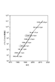
- FIG. 24 is a graph showing the tendency of miniaturization of semiconductor devices, with the horizontal axis representing the age and the vertical axis representing the degree of integration of transistors.
- the degree of integration of semiconductor devices has increased exponentially according to Moore's law. Along with this, the pattern of semiconductor devices has become finer. In recent years, devices having a transistor channel length of 10 nm or less have also been announced. Therefore, the mask pattern used for patterning is also required to be miniaturized, and for example, the line width needs to be 10 nm or less.
- the shape error becomes relatively large, so the shape error, which was not a problem before, will no longer be acceptable. For example, a slight shape error will significantly reduce the yield of the semiconductor device. Therefore, the controllability required for patterning becomes stricter.
- low-level dust and pollution which were not previously a problem, will become a problem in the future. Therefore, in the future, higher controllability will be required for various processes constituting the manufacturing process of semiconductor devices. In particular, improvement of patterning controllability is a decisive requirement for miniaturization of semiconductor devices.
- plasma etching the portion not covered by the mask pattern is physicochemically etched using ions and radicals excited by plasma.
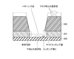
- FIG. 25 (a) to 25 (e) are cross-sectional views showing a general plasma etching process.
- FIG. 26 is a diagram showing typical factors to be controlled by plasma etching.
- the base member 300 is prepared.
- the base member 300 may be a washed substrate or a thin film formed on the substrate.
- the thin film 301 is deposited on the entire surface of the base member 300.
- the method of depositing the thin film 301 is, for example, sputtering or CVD (Chemical Vapor Deposition) or the like.
- a photoresist is applied onto the thin film 301, exposed, and developed to form a resist pattern 302 in which a predetermined pattern is formed.
- the thin film 301 is patterned by performing etching using plasma using the resist pattern 302 as a mask.
- ashing is performed to remove the resist pattern 302. In this way, the thin film 301 is patterned into a predetermined shape.
- factors that determine the controllability of plasma etching include the dimensions of the resist pattern 302, the shape of the thin film 301, the etching selectivity between the resist pattern 302 and the thin film 301, and the thin film 301 and the base member 300.
- Large dimensional factors related to pattern formation such as etching selectivity and etching residue of the thin film 301.
- contamination by impurities caused by plasma etching equipment and etching gas, structural changes of the underlying member due to ion injection, and the like also have a large effect on the electrical characteristics of the semiconductor device.
- the residue of the etching product, the structural change of the mask pattern, and the like are factors that affect the controllability in the next step and thereafter.
- the channel length of the transistor will vary. Therefore, the electrical characteristics of the transistor are directly affected.
- the plasma etching step shown in FIG. 26 is a step of forming wiring, and when the wiring is embedded with an insulating film in the subsequent step, voids (voids) are formed in the insulating film. Is formed, the capacitance between the wirings may change, the signal may be delayed, or the reliability may decrease. Further, if the etching product remains at the connection portion between the wiring and the transistor, the electric resistance increases, which causes wiring delay and disconnection failure.
- the etching selectivity between the thin film 301 and the base member 300 is lowered, so-called overetching occurs when the thin film 301 is etched, and the base member 300 is also etched. Therefore, the shape accuracy is lowered. Further, when the over-etching is remarkable, the recess formed by the over-etching penetrates the base member 300 and reaches the member (not shown) further below.
- the lower member and the thin film 301 are conductive members and the base member 300 is an insulating film, the conductive members that should be originally insulated come into contact with each other, causing short circuits and leaks, and the semiconductor device is normally operated. It stops working.
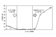
- FIG. 27 is a graph showing a margin of an allowable etching amount, with the horizontal axis representing the etching time and the vertical axis representing the defect rate.
- the etching amount is often controlled by the etching time. As shown in FIG. 27, if the etching amount is insufficient, etching residue is generated and the product becomes defective, and if the etching amount is excessive, the base member is excessively etched, and the product is also defective.
- the allowable etching amount is such that no etching residue is generated and the etching amount of the base member is equal to or less than the allowable amount. However, as the semiconductor device becomes finer, this margin becomes narrower. Become.
- the etching characteristics of the equipment will not always be completely uniform after maintenance. For example, a slight mounting error between parts affects the etching characteristics. This not only causes an error in each maintenance of the same device, but also causes an error between the devices, and when multiple chambers are provided in one device to improve productivity, even between the chambers. There will be an error.
- the present invention has been made in view of the above-mentioned problems, and an object of the present invention is to provide a plasma processing apparatus, a plasma processing method, and a conductive member having stable operation.
- the plasma processing apparatus is arranged between a chamber having a first member, a second member that can be attached to and detached from the first member, and the first member and the second member. It includes a conductive member and a first high-frequency power source that generates plasma in the chamber.
- the conductive member has a resin member made of a resin material and a metal film provided on the surface of the resin member.
- a member to be treated is charged in a chamber including a first member and a second member, and a resin member made of a resin material is placed between the first member and the second member.
- a step of arranging a conductive member provided with a metal film on the surface of the chamber and compressing the conductive member, and a step of generating plasma in the chamber by applying a high frequency current are provided.
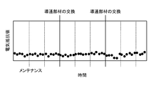
- the horizontal axis is time
- the vertical axis is the electric resistance value between the lower part and the upper part of the chamber.
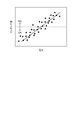
- the horizontal axis represents the electric power supplied to the holder, and the vertical axis represents the etching amount.
- the graph shows an example of the relationship between the supplied power and the etching amount. It is sectional drawing which shows the plasma etching apparatus which concerns on 1st Embodiment.
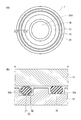
- (A) is a plan view showing the lower part of the plasma etching apparatus according to the first embodiment, and (b) is a cross-sectional view taken along the line AA'shown in (a).
- (A) is a perspective view showing a conduction member of the plasma etching apparatus according to this embodiment, and (b) is a sectional view thereof.
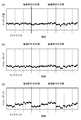
- (A) is a graph showing an example of the relationship between the etching amount and maintenance and parts replacement in the plasma etching apparatus according to the first embodiment, with time on the horizontal axis and etching amount on the vertical axis.
- b) is a graph showing an example of the relationship between impedance and maintenance and component replacement in the plasma etching apparatus according to the first embodiment, with time on the horizontal axis and impedance on the vertical axis. It is a graph which shows an example of the relationship between impedance and maintenance, and component replacement in the plasma etching apparatus which concerns on comparative example, which takes time on the horizontal axis and impedance on the vertical axis.
- A) is a cross-sectional view showing the shape of the conductive member when the chamber is released
- (b) is a cross-sectional view showing the shape of the conductive member when the chamber is closed
- (c) is a state in which a crack is generated in the metal film.
- the compressibility is taken on the horizontal axis
- the electric resistance value is taken on the vertical axis
- the compressive force is repeatedly applied to the conductive member having a metal film made of nickel and a thickness of 400 nm while changing the compressibility.
- (b) shows the compressibility at the time of compression for the data shown in (a) on the horizontal axis
- the electric resistance value at the time of compression and release on the vertical axis It is a graph which shows the influence which the compressibility has on the electric resistance value.
- the compressibility is taken on the horizontal axis
- the electric resistance value is taken on the vertical axis
- the compressive force is repeatedly applied to the conductive member having a metal film made of nickel and a thickness of 800 nm while changing the compressibility.
- (b) shows the compressibility at the time of compression for the data shown in (a) on the horizontal axis
- the electric resistance value at the time of compression and release on the vertical axis It is a graph which shows the influence which the compressibility has on the electric resistance value.
- the compressibility is taken on the horizontal axis
- the electric resistance value is taken on the vertical axis
- the compressive force is repeatedly applied to the conductive member having a metal film made of copper and a thickness of 100 nm while changing the compressibility.
- (b) shows the compressibility at the time of compression for the data shown in (a) on the horizontal axis
- the electric resistance value at the time of compression and release on the vertical axis It is a graph which shows the influence which the compressibility has on the electric resistance value.
- the compressibility is taken on the horizontal axis
- the electric resistance value is taken on the vertical axis
- the compressive force is repeatedly applied to the conductive member having a metal film made of copper and a thickness of 400 nm while changing the compressibility.
- (b) shows the compressibility at the time of compression for the data shown in (a) on the horizontal axis
- the electric resistance value at the time of compression and release on the vertical axis It is a graph which shows the influence which the compressibility has on the electric resistance value.
- the compressibility is taken on the horizontal axis
- the electric resistance value is taken on the vertical axis
- the compressive force is repeatedly applied to the conductive member having a metal film made of copper and a thickness of 800 nm while changing the compressibility.
- (b) shows the compressibility at the time of compression for the data shown in (a) on the horizontal axis
- the electric resistance value at the time of compression and release on the vertical axis It is a graph which shows the influence which the compressibility has on the electric resistance value.
- the horizontal axis is the compressibility at the time of compression
- the vertical axis is the electric resistance value at the time of release.
- (A) is a cross-sectional view showing a conductive member of the plasma etching apparatus according to the second embodiment
- (b) is a perspective view showing a conductive member in an open state
- (c) is a conductive member in a compressed state. It is a perspective view which shows.
- (A) is a plan view showing a test material to be etched in a test example
- (b) is a cross-sectional view showing a test material before etching treatment
- (c) is a cross-sectional view showing a test material after etching treatment. It is a figure.
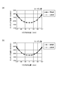
- (A) and (b) are graphs showing the etching rate distribution with respect to the carbon film, with positions on the horizontal axis and etching rates on the vertical axis.
- (A) and (b) are graphs showing the etching rate distribution with respect to the silicon oxide film, with positions on the horizontal axis and etching rates on the vertical axis.
- (A) and (b) are graphs showing the etching rate distribution with respect to the silicon nitride film, with the horizontal axis representing the position and the vertical axis representing the etching rate. It is a graph which shows the presence or absence of nickel contamination by taking a sample on the horizontal axis and taking the amount of nickel detected in the test material after etching on the vertical axis. It is a graph which shows the tendency of miniaturization of a semiconductor device by taking the age on the horizontal axis and the degree of integration of transistors on the vertical axis.
- (A) to (e) are cross-sectional views showing a general plasma etching process. It is a figure which shows the typical factor which should be controlled by plasma etching.
- FIG. 28 is a diagram showing an example of factors that affect the controllability of etching. As shown in FIG. 28, at least the following factors can be considered as factors that affect the controllability of etching.
- Variation of gas composition, flow rate, and pressure as plasma species (2) Variation of output of high frequency power supply for forming plasma (3) Variation of processing temperature (4) Variation of high frequency power supply for applying bias Output variation (5) Bias voltage and etching rate calibration line deviation (6) Damage and repair of each part in the chamber due to etching (7) Deterioration and replacement of parts that make up the plasma processing device
- the purchased high-purity gas is usually introduced by controlling the flow rate directly from the supply line into the chamber. Therefore, unless there is a leak in the air supply pipe or the chamber, it is unlikely that the variation in the composition of the plasma species is the cause of the variation in the etching rate. Further, since the gas flow rate and pressure can be easily controlled and measured, it is unlikely that the gas flow rate and pressure will fluctuate greatly.
- the processing amount is not always excessive, but is normal, too small, or excessive. Or something. Therefore, unless there is a failure in the high-frequency power supply, it is unlikely that the variation in the output of the high-frequency power supply is the cause of the variation in the etching rate. Further, since the same variation occurs in many plasma processing devices, it is unlikely that the high frequency power supply is out of order.
- the temperature of the wafer during plasma processing may vary due to various factors.
- the wafer temperature can be measured directly, and no significant relationship is found between the measured wafer temperature and the etching amount. Therefore, the influence of the variation in the processing temperature on the etching rate is considered to be limited, if any.
- the processing amount is not always excessive, and it may be normal or insufficient. .. Therefore, it is unlikely that the deviation of the calibration curve is the cause of the variation in the etching rate, and even if the accuracy of the calibration curve is further improved, the effect of converging the variation in the etching rate is considered to be small.
- ICP inductively coupled plasma
- FIG. 29 is a diagram showing an example of a general inductively coupled plasma type dry etching apparatus.
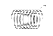
- FIG. 30 is a perspective view showing a conductive member.
- the plasma etching apparatus 100 is provided with a chamber 101.
- the chamber 101 is composed of a lower portion 102 and an upper portion 103. Normally, the lower portion 102 is fixed to a frame or the like and is grounded.
- the upper portion 103 is provided so as to be openable and closable with respect to the lower portion 102, and functions as a lid of the chamber 101.
- a holder 106 is provided in the lower portion 102.
- the holder 106 holds the wafer 200 as a member to be processed.
- the holder 106 is connected to the high frequency power supply 108 via the voltage control unit 107.
- the voltage control unit 107 and the high frequency power supply 108 are each grounded.
- a dielectric plate 109 is provided on the upper portion 103, a coil 110 is provided on the dielectric plate 109, and the coil 110 is connected to a high frequency power supply 111.
- the high frequency power supply 111 is also grounded.
- an airtight member 115 for ensuring airtightness in the chamber 101 and a conductive member 116 for ensuring continuity between the lower portion 102 and the upper portion 103 are provided. ..
- the airtight member 115 is, for example, an O-ring
- the conductive member 116 is, for example, a metal coil.
- the lower portion 102 and the upper portion 103 are connected by metal bolts and nuts. As a result, the lower portion 102 and the upper portion 103 are mechanically bonded and equipotential.
- the chamber 101 is provided with an air supply pipe 118 for supplying gas into the chamber 101 and an exhaust pipe 119 for discharging gas from the inside of the chamber 101.
- the conductive member 116 is a coil-shaped member formed by winding a metal band in a spiral shape.
- a groove slightly shallower than the diameter of the conductive member 116 is formed on the surface of the lower 102 of the chamber 101 that comes into contact with the upper portion 103, and the conductive member 116 is housed in this groove.
- the wafer 200 is mounted on the holder 106. Further, the upper portion 103 is connected to the lower portion 102 to make the inside of the chamber 101 airtight. Then, the inside of the chamber 101 is exhausted through the exhaust pipe 119, and a gas serving as a plasma species is introduced through the air supply pipe 118. In this state, the high frequency power supply 111 supplies the high frequency current to the coil 110. As a result, the gas is ionized to form the plasma 250. Further, the high frequency power supply 108 supplies a high frequency current to the holder 106. As a result, a bias voltage is applied to the plasma 250, the ions in the plasma are accelerated, and the ions collide with the wafer 200. As a result, the wafer 200 is etched.
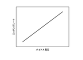
- FIG. 31 is a graph showing the bias voltage dependence of the etching rate, with the horizontal axis representing the bias voltage and the vertical axis representing the etching rate.
- the higher the bias voltage the higher the accelerating voltage of the ions and the higher the etching rate.
- This correlation differs depending on the material of the member to be processed, the design of the device, and the individual difference of the device. Therefore, the relationship between the bias voltage and the etching rate is calibrated in advance.
- the bias voltage corresponding to the target etching rate is input to the voltage control unit 107.
- the voltage control unit 107 controls the output of the high frequency power supply 108 to realize a desired etching rate.
- the wafer 200 is etched in a certain amount.
- FIG. 1 is a graph showing an example of the relationship between the etching amount and maintenance and component replacement in a conventional plasma etching apparatus, with time on the horizontal axis and etching amount on the vertical axis.
- FIG. 1 shows the results of a survey on one plasma etching apparatus.
- the broken line extending in the vertical direction in the drawing represents the maintenance timing
- the solid line represents the replacement timing of the conductive member 116.
- FIG. 2 which will be described later.
- the drawings attached to the present specification are basically schematic views. It is created based on actual data, but does not represent an absolute value.
- the etching amount tended to increase with each maintenance of the above (6) and decrease after the replacement of the conductive member 116 of the above (7).
- the replacement cycle of the conductive member 116 is longer than the maintenance cycle, and the conductive member 116 is replaced once every several maintenances.
- the results shown in FIG. 1 suggest that the maintenance and conduction member 116 contributes to the variation in etching rate.
- the conductive member 116 is a component that electrically connects the lower portion 102 and the upper portion 103 of the chamber 101.
- FIG. 2 is a graph showing an example of the relationship between the replacement time of the conductive member and the electric resistance value, with time on the horizontal axis and the electric resistance value between the lower part and the upper part of the chamber on the vertical axis. As shown in FIG. 2, the electric resistance value was stable and low, and sufficient conduction was obtained between the lower portion 102 and the upper portion 103. In addition, no correlation was found between the maintenance time and the replacement time of the conductive member 116 and the electrical resistance value.
- the present inventors have made the following hypothesis. Since the etching amount changes discontinuously at the time of maintenance and the time of replacement of the conductive member 116, it is presumed that the maintenance and the conductive member 116 affect the etching conditions. On the other hand, the electric resistance value of the direct current and the impedance of the high frequency current are not necessarily the same, and even if the direct current is sufficiently conducted between the lower 102 and the upper 103 of the chamber 101, the high frequency current is not sufficiently conducted. Is also possible. Therefore, it is considered that the impedance of the conductive member 116 does not change but the impedance increases with the maintenance.
- the upper part 103 When performing maintenance, the upper part 103 is removed from the lower part 102, and the chamber 101 is opened. Then, after performing necessary measures such as repairing the portion damaged by etching, the upper portion 103 is fixed to the lower portion 102, and the chamber 101 is closed. Each time this work is performed, the conductive member 116 repeats compression and release. Since the conductive member 116 is made of metal, it elastically deforms when a compressive force is applied, but at this time, plastic deformation also occurs locally.
- the conductive member 116 when the conductive member 116 is repeatedly deformed by opening and closing the chamber 101, the force with which the conductive member 116 presses the lower portion 102 and the upper portion 103 decreases, and even if the DC electric resistance value does not change, the high frequency power supply 108 and The impedance to the high frequency current output by 111 may be increasing.
- the average potential of the upper 103 deviates from the average potential of the lower 102, and the ground potential referenced by the voltage control unit 107 and the ground potential seen from the plasma 250 deviate from each other.
- the ground potential seen from the plasma 250 is considered to be the average potential of the inner wall of the chamber 101. Therefore, even if the bias voltage is adjusted according to the calibration curve shown in FIG. 31, the etching amount deviates from the calibration curve shown in FIG. 31. As a result, it is estimated that the etching amount may be excessive.
- FIG. 3 is a graph showing the relationship between the supplied power and the etching amount, with the horizontal axis representing the power supplied to the holder and the vertical axis representing the etching amount.
- the etching amount showed a positive correlation with the input power, and when the etching was excessive, the input power was also excessive.
- the high-frequency power supply 108 has a bias voltage higher than the set value from the voltage control unit 107. It is considered that such a control signal is input.
- the bias voltage acting on 250 is different from the set value.
- the cause is an increase in impedance of the conductive member 116 with respect to high frequency power.
- the cause of the increase in impedance is considered to be plastic deformation of the conductive member 116.
- the result shown in FIG. 1 is interpreted based on such an estimation as follows. That is, when maintenance is performed, the impedance between the parts increases and the ground potential shifts, so that the etching amount per unit time tends to increase. However, by replacing the conductive member 116 (see FIG. 30) installed between the parts with a new one, the impedance tends to decrease and the etching amount per unit time tends to return to the initial state.
- Fig. 3 The result shown in Fig. 3 is interpreted as follows.
- the self-bias of the plasma is measured, and the input power is controlled so that the value approaches the set value.
- the magnitude of this input power is shown on the horizontal axis in FIG. Due to the change in impedance between the lower part 102 and the upper part 103 of the chamber 101, the ground potential referred to when measuring the self-bias of plasma shifts, and an error depending on the impedance occurs in the measured value of self-bias. Therefore, an error also occurs in the input power controlled based on this measured value. As described above, an error occurs in the input power depending on the impedance between the lower portion 102 and the upper portion 103, and as a result, an error also occurs in the etching amount per unit time.
- the present inventors have studied a policy for solving the problem.
- a new conductive member instead of the conductive member 116 in which the metal band is formed into a coil shape.
- the new conductive member is required to be elastically deformable, substantially free from plastic deformation, and capable of conducting a high-frequency current.
- a resin material can be considered as a material that is elastically deformed and does not undergo plastic deformation.
- the resin material is not conductive as it is. Therefore, it is required to impart conductivity to the resin material.
- a method of imparting conductivity to the resin material As a method of imparting conductivity to the resin material, a method of containing conductive particles such as carbon black or a metal filler in the resin material and a method of coating a metal on the surface can be considered.
- a high-frequency current is passed through a conductor, the higher the frequency, the more the current concentrates on the surface. Therefore, it is expected that the impedance of the high-frequency current can be effectively reduced by coating the surface of the member made of the resin material with a metal rather than containing the conductive particles in the resin material.
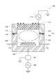
- FIG. 4 is a cross-sectional view showing a plasma etching apparatus according to the present embodiment.
- FIG. 5A is a plan view showing the lower part of the plasma etching apparatus according to the present embodiment
- FIG. 5B is a cross-sectional view taken along the line AA'shown in FIG. 5A.
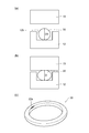
- FIG. 6A is a perspective view showing a conductive member of the plasma etching apparatus according to the present embodiment
- FIG. 6B is a cross-sectional view thereof.
- the plasma etching apparatus 1 is provided with the chamber 11.
- a lower portion 12 and an upper portion 13 are provided.
- the lower portion 12 is fixed to a frame or the like and is grounded.
- the upper portion 13 is detachably provided with respect to the lower portion 12, and is not grounded.
- the chamber 11 is opened and closed by attaching and detaching the upper portion 13 to the lower portion 12. There is a slight gap between the lower portion 12 and the upper portion 13. The gap interval is, for example, 0.3 mm or less.
- the chamber 11 is provided with an air supply pipe 28 for supplying gas into the chamber 11 and an exhaust pipe 29 for discharging gas from the inside of the chamber 11.
- a holder 16 is provided in the lower portion 12.
- the holder 16 holds the wafer 200, which is a member to be processed.
- the holder 16 is connected to the high frequency power supply 18 via the voltage control unit 17.
- the voltage control unit 17 and the high frequency power supply 18 are each grounded.
- the high frequency power supply 18 outputs, for example, a high frequency current having a frequency of 13.56 MHz.
- a dielectric plate 19 is provided on the upper portion 13, and a coil 20 is provided on the dielectric plate 19.
- the coil 20 is fixed to the upper portion 13.
- the coil 20 is connected to the high frequency power supply 21.
- the high frequency power supply 21 is also grounded.
- the high frequency power supply 21 outputs, for example, a high frequency current having a frequency of 13.56 MHz.
- an airtight member 15 for ensuring airtightness in the chamber 11 and a conductive member 30 for ensuring continuity between the lower portion 12 and the upper portion 13 are provided. .. That is, an annular groove 12a is formed on the upper surface of the lower portion 12, and an annular groove 12b is formed on the outside of the groove 12a. An airtight member 15 is arranged in the groove 12a. The airtight member 15 is, for example, an O-ring. A conductive member 30 is arranged in the groove 12b. In this way, the conductive member 30 is arranged outside the airtight member 15. Further, the lower portion 12 and the upper portion 13 are connected by metal bolts and nuts. As a result, the lower portion 12 and the upper portion 13 are mechanically coupled, and the airtight member 15 and the conductive member 30 are pressed by the lower portion 12 and the upper portion 13.
- the overall shape of the conductive member 30 of this embodiment is annular.
- the entire surface of the resin ring 31 made of the resin material is covered with the metal film 32 made of the metal material.
- the ring diameter R0 of the conductive member 30 depends on the outer diameter of the chamber 11. For example, when the diameter of the wafer 200 is 300 mm (millimeters), the ring diameter R0 is about 600 mm.
- the diameter D0 of the conductive member 30 is, for example, about 2 to 4 mm (millimeters).
- the film thickness T0 of the metal film 32 is, for example, 200 nm (nanometers) or more.
- the conductive member 30 preferably has a maximum diameter of 2 mm or more and 4 mm or less in the compression direction when the compressibility is compressed in the range of 5% or more and 25% or less.
- the resin material forming the resin ring 31 is, for example, elastic rubber, for example, fluororubber, for example, FKM-70.
- the elastic modulus of the resin ring 31 is, for example, 10 MPa.
- the diameter of the resin ring 31 is, for example, 3 mm, and the Poisson ratio is about 0.5.
- the film structure of the metal film 32 may be, for example, a single-layer film made of nickel (Ni) or copper (Cu), or a multilayer film in which two or more layers are laminated.
- the metal film 32 can be adhered to the surface of the resin ring 31 by, for example, intermolecular adhesive bonding. Specifically, after the resin ring 31 is formed, the resin ring 31 is subjected to a corona discharge treatment to generate OH groups on the surface. Next, the resin ring 31 is brought into contact with alkoxysilylpropylamide triazinethiol to form a dithioltriazine group on the surface. Next, the resin ring 31 is immersed in the plating solution. As a result, the metal ions in the plating solution chemically bond with the dithioltriazine group to form the metal film 32. As a result, a high adhesion force can be realized between the resin ring 31 and the metal film 32.
- the operation of the plasma processing apparatus according to the present embodiment that is, the plasma processing method according to the present embodiment will be described.
- the chamber 11 when maintaining the inside of the chamber 11, the chamber 11 is opened by removing the upper portion 13 from the lower portion 12. At this time, the compressive force applied to the conductive member 30 is removed. In this state, perform necessary maintenance. After the maintenance is completed, the airtight member 15 is arranged in the groove 12a of the lower portion 12, and the upper portion 13 is connected to the lower portion 12 with the conductive member 30 arranged in the groove 12b. As a result, the conductive member 30 is compressed.
- the wafer 200 When plasma etching is performed on the wafer 200, the wafer 200 is mounted on the holder 16 via the load lock portion of the chamber 11. Then, the inside of the chamber 11 is exhausted through the exhaust pipe 29, and a gas serving as a plasma species is introduced through the air supply pipe 28. In this state, the high frequency power supply 21 supplies a high frequency current to the coil 20. As a result, the gas is ionized to form the plasma 250. Further, the high frequency power supply 18 supplies a high frequency current to the holder 16. As a result, a bias voltage is applied to the plasma 250, the ions in the plasma are accelerated, and the ions collide with the wafer 200. As a result, the wafer 200 is etched. At this time, a high frequency current is conducted between the lower portion 12 and the upper portion 13 via the conductive member 30.
- the resin ring 31 is made of a resin material and therefore does not undergo plastic deformation. Therefore, the force of pressing the metal film 32 against the lower portion 12 and the upper portion 13 due to the plastic deformation does not decrease. As a result, an increase in the impedance of the metal film 32 can be suppressed.
- the metal film 32 may be plastically deformed due to the above-mentioned deformation of the resin ring 31, but the force pressing the metal film 32 against the lower portion 12 and the upper portion 13 is not the metal film 32 itself but the elasticity of the resin ring 31. It is due to force. Therefore, even if the metal film 32 is plastically deformed, the pressing force does not change, and the impedance does not increase significantly due to the plastic deformation of the metal film 32. Further, since most of the volume of the conductive member 30 is occupied by the insulating resin ring 31, the electric resistance value of the conductive member 30 with respect to the direct current is higher than the electric resistance value of the conventional conductive member 116 shown in FIG. Sometimes. However, as described above, the high-frequency current is concentrated on the surface layer portion of the conductive member 30, and the metal film 32 is arranged in this portion, so that the impedance with respect to the high-frequency current is sufficiently low.
- FIG. 7A is a graph showing an example of the relationship between the etching amount and maintenance and component replacement in the plasma etching apparatus according to the present embodiment, with time on the horizontal axis and etching amount on the vertical axis.
- (B) is a graph showing an example of the relationship between impedance and maintenance and component replacement in the plasma etching apparatus according to the first embodiment, with time on the horizontal axis and impedance on the vertical axis.
- Is a graph showing an example of the relationship between impedance and maintenance and component replacement in a plasma etching apparatus according to a comparative example, with time on the horizontal axis and impedance on the vertical axis.
- the etching amount does not change significantly, and stable operation is possible.
- FIG. 7B according to the present embodiment, even if maintenance and replacement of the conductive member 30 are performed, the change in impedance between the lower portion 12 and the upper portion 13 is small, and stable operation can be performed. It was confirmed that it was possible.
- the impedance between the lower portion 102 and the upper portion 103 was measured.
- FIG. 7C in the plasma etching apparatus 100 according to the comparative example, due to the deformation of the conductive member 116 (see FIG. 30) due to the maintenance, the lower part after the maintenance.
- the impedance between 102 and the upper 103 has increased.
- the impedance tended to return to the initial value by replacing the conductive member 116 with a new one.
- a one-to-one correlation was observed between this change in impedance and the amount of etching per unit time.
- the conductive member 30 is provided with the resin material, for example, the resin ring 31 made of elastic rubber and the metal film 32 covering the surface of the resin ring 31, the chamber Even if the opening and closing of 11 is repeated, the elastic force of the resin ring 31 does not decrease. Therefore, it is possible to suppress an increase in impedance between the lower portion 12 and the upper portion 13 and suppress a deviation in the etching rate. As a result, the plasma etching process can be stably performed.
- the conductive member 30 is soft as a whole. Therefore, as compared with the conductive member 116 made of a metal band, it is easier to mount the lower portion 12 in the recess 12b.
- the dimensions and the like of each part differ depending on the required specifications, so the problem is how to design the plasma etching apparatus 1 including the conductive member 30.
- the ring diameter R0 of the conductive member 30 is determined according to the size of the chamber 11, and the size of the chamber 11 is determined by the size of the wafer 200 which is a member to be processed.
- the diameter D0 of the conductive member 30 is determined in consideration of the compressibility.
- FIG. 8A is a cross-sectional view showing the shape of the conductive member 30 when the chamber is open
- FIG. 8B is a cross-sectional view showing the shape of the conductive member 30 when the chamber is closed
- FIG. 8C is a metal film 32. It is a photograph which shows the conduction member 30 in the state where a crack is generated.
- the compressibility C is defined as the following mathematical formula 1.
- C (D0-D) / D0 ⁇ 100 [%] (Formula 1)
- the horizontal axis represents the compressibility
- the vertical axis represents the electrical resistance value
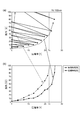
- the conductive member having the metal film 32 made of nickel and having a thickness of 100 nm is repeatedly compressed while changing the compressibility.
- (b) is the compressibility at the time of compression for the data shown in (a) on the horizontal axis
- the electric resistance at the time of compression and release on the vertical axis It is a graph which takes a value and shows the influence which a compressibility has on an electric resistance value.
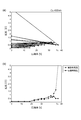
- 10 (a) to 14 (b) are the same graphs as in FIGS. 9 (a) and 9 (b).
- 10 (a) and 10 (b) show a case where the metal film 32 is made of nickel and has a thickness of 400 nm
- FIGS. 11 (a) and 11 (b) show a case where the metal film 32 is made of nickel and has a thickness of 800 nm
- 12 (a) and 12 (b) show the case where the metal film 32 is made of copper and the thickness is 100 nm
- FIGS. 13 (a) and 13 (b) show the case where the metal film 32 is made of copper.
- the case where the thickness is 400 nm is shown
- FIGS. 14 (a) and 14 (b) show the case where the metal film 32 is made of copper and the thickness is 800 nm.
- the horizontal axis represents the compression rate at the time of compression
- the vertical axis represents the electric resistance value at the time of release, showing the influence of the composition and film thickness of the metal film on the relationship between the compression rate and the electric resistance value.
- FIG. 16 is a graph showing a suitable range of use of the conductive member, with the horizontal axis representing the film thickness of the metal film and the vertical axis representing the compressibility immediately before the resistance value shows an irreversible change.
- the resistance to compression is higher when the metal film 32 is formed of copper than when it is formed of nickel. Further, if the materials of the metal film 32 are the same, the thicker the film thickness, the higher the resistance to compression.
- the critical value Tc of the compressibility according to the composition and the film thickness of the metal film 32, as shown in FIG. 16 the range of the compressibility at which the conductive member 30 can be used repeatedly can be obtained. ..
- the relationship between the diameter D0 of the conductive member 30 and the depth of the groove 12b formed in the lower portion 12 can be determined.
- the compressibility is preferably 25% or less, and when the film thickness is 400 nm or more, the compressibility is 30% or less.
- the compressibility is preferably 35% or less.
- the compressibility is preferably 35% or less.
- the film thickness of the metal film 32 is preferably 100 nm or more and 2000 nm or less, and more preferably 100 nm or more and 1000 nm or less.
- the material of the metal film 32 is not limited to nickel and copper.
- Examples of the material of the metal film 32 include nickel (Ni), chromium (Cr), titanium (Ti), tungsten (W), cobalt (Co), gold (Au), silver (Ag), copper (Cu), and tin.
- One or more metals selected from the group consisting of (Sn) and zinc (Zn) may be used.
- the metal film 32 may be a multilayer film.
- the metal film 32 may be a three-layer film composed of a base layer, a main layer, and a surface layer in this order from the resin ring 31 side.
- a material having a dense crystal structure and high chemical stability for example, nickel is used
- a material having excellent ductility for example, copper is used.
- the surface material a material having excellent chemical stability and conductivity, for example, gold may be used. That is, the metal film 32 may be a (Ni / Cu / Au) three-layer film.
- the base layer and the surface layer may be formed of nickel, and the main layer may be formed of copper. That is, the metal film 32 may be a (Ni / Cu / Ni) three-layer film. In this case, for example, the thickness of the base layer and the surface layer may be 100 nm, and the thickness of the main layer may be 400 nm.
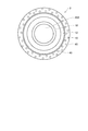
- FIG. 17 is a plan view showing the lower part of the plasma etching apparatus according to the present embodiment.
- FIG. 18A is a cross-sectional view showing a conductive member of the plasma etching apparatus according to the present embodiment,
- FIG. 18B is a perspective view showing a conductive member in an open state, and
- FIG. 18C is a conductive member in a compressed state. It is a perspective view which shows.
- each conducting member 40 is not an annular shape but a spherical shape.
- a cylindrical recess is formed on the upper surface of the lower portion 12 of the chamber 11, and the conductive member 40 is housed in the recess.
- Each conductive member 40 is provided with a resin ball 41 made of a resin material, for example, elastic rubber, for example, fluororubber, and a metal film 42 is coated on the surface of the resin ball 41.
- the composition and film thickness of the metal film 42 are the same as those of the metal film 32 in the first embodiment.
- the conductive member 40 does not necessarily have to be annular. As in the present embodiment, a massive, for example, spherical conductive member 40 may be provided. Further, by providing a plurality of conductive members 40, low impedance can be realized in each part of the chamber 11.
- the conductive member 40 is spherical, when compressed in the uniaxial direction, for example, in the Z-axis direction shown in FIGS. 18 (b) and 18 (c).
- it can be extended in other biaxial directions, for example, in the X-axis direction and the Y-axis direction.
- the stretching ratio per axis is reduced, and the mechanical stress applied to the metal film 42 is dispersed.
- the metal film 42 can withstand higher compressibility. Therefore, the conductive member 40 can be used with a higher compressibility, and the impedance can be reduced more reliably.
- the shape of the conductive member 40 preferably satisfies the following mathematical formula 2.
- the following formula 2 is an inequality of Euler's formula.
- P is the load applied to the conductive member 40
- P cr is the buckling load of the conductive member 40
- C is the terminal condition coefficient
- ⁇ is the pi
- E is Young's modulus
- I is the moment of inertia of area.
- L is the length.
- the plasma etching apparatus has been described as an example of the plasma processing apparatus, but the plasma processing apparatus is not limited to the etching apparatus, and for example, plasma CVD (Chemical Vapor Deposition) is used. ) It may be a film forming apparatus such as an apparatus.
- plasma CVD Chemical Vapor Deposition
- Example> the plasma etching apparatus 1 according to the first embodiment shown in FIGS. 4, 5 (a) and 5 (b), and FIGS. 6 (a) and 6 (b) was actually manufactured, and this was referred to as " Example ”.
- the material of the metal film 32 of the conductive member 30 was nickel, and the thickness was 400 nm.
- the general plasma etching apparatus 100 shown in FIGS. 29 and 30 was actually manufactured and used as a "comparative example". Then, the test material was subjected to an etching treatment by the apparatus according to the example and the apparatus according to the comparative example, and the distribution of the etching rate in the test material was measured.
- FIG. 19A is a plan view showing a test material to be etched in this test example
- FIG. 19B is a cross-sectional view showing a test material before etching treatment
- FIG. 19C is a test material after etching treatment. It is sectional drawing which shows.
- the silicon wafer 301 is provided in the test material 300 used in this test example.
- a notch 301n is formed in the silicon wafer 301.
- the direction from the center 301c of the silicon wafer 301 toward the notch 301n is defined as the "X direction”
- the direction orthogonal to the X direction is defined as the "Y direction”.
- the following films are sequentially laminated on the silicon wafer 301.
- the numbers in parentheses indicate the thickness of each film.
- the silicon oxide film 304 was formed by a CVD method using TEOS (Tetraethyl orthosilicate: Tetraethyl orthosilicate: Si (OC 2 H 5 ) 4 ) as a raw material.
- the silicon oxide film 306 was formed by a coating method.
- a predetermined pattern was formed on the resist pattern 310 by a lithography method.
- test materials 300 Two of these test materials 300 were prepared and subjected to RIE (Reactive Ion Etching) by the plasma etching apparatus according to the example and the comparative example. Although the etching conditions are adjusted according to the film to be etched, they are the same between the examples and the comparative examples.
- RIE Reactive Ion Etching
- the silicon oxide film 306 was patterned by etching the silicon oxide film 306 using the resist pattern 310 as a mask. Then, the resist pattern 310 was removed.
- the carbon film 305 was patterned by etching the carbon film 305 using the patterned silicon oxide film 306 as a mask. At this time, the etching rate distribution of the carbon film 305 in the plane of the test material 300 was measured.
- the silicon oxide film 304 was patterned by etching the silicon oxide film 304 using the patterned carbon film 305 as a mask. At this time, the etching rate distribution of the silicon oxide film 304 in the plane of the test material 300 was measured. Then, the residue generated by the etching of the silicon oxide film 304 was removed.
- the silicon nitride film 303 was patterned by etching the silicon nitride film 303 using the patterned carbon film 305 and the silicon oxide film 304 as masks. At this time, the etching rate distribution of the silicon nitride film 303 in the plane of the test material 300 was measured.
- 20 (a) and 20 (b) are graphs showing the etching rate distribution with respect to the carbon film 305, with positions on the horizontal axis and etching rates on the vertical axis.
- 21 (a) and 21 (b) are graphs showing the etching rate distribution with respect to the silicon oxide film 304, with positions on the horizontal axis and etching rates on the vertical axis.
- 22 (a) and 22 (b) are graphs showing the etching rate distribution with respect to the silicon nitride film 303, with positions on the horizontal axis and etching rates on the vertical axis.
- the horizontal axis of each figure represents the position of the silicon wafer 301 in the X direction or the Y direction, and the position of the center 301c is “0”.
- the etching rate has a distribution in the plane of the test material 300, the etching rate and its distribution are substantially different between the examples and the comparative examples. It was the same. Therefore, it has been found that even if the conventional plasma etching apparatus is replaced with the plasma etching apparatus according to the first embodiment, it is not necessary to readjust the etching conditions and it can be continuously used.
- the metal film 32 of the conductive member 30 is formed of nickel, there is a concern that the inside of the apparatus may be contaminated with nickel. Therefore, the amount of nickel was measured in the test material 300 after etching.
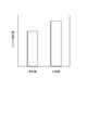
- FIG. 23 is a graph showing the presence or absence of nickel contamination by taking a sample on the horizontal axis and the amount of nickel detected in the test material after etching on the vertical axis.
- the detected amount of nickel in the examples was equal to or less than the detected amount of nickel in the comparative example. Therefore, it can be said that nickel contamination caused by the conductive member 30 has not occurred.
- the amount of dust generated in the examples was equal to or less than that in the comparative examples, and satisfied the current standard.
- the plasma etching apparatus 1 according to the embodiment has substantially the same etching rate and distribution thereof as compared with the plasma etching apparatus 100 according to the comparative example, and contamination due to the conductive member 30 is also observed. However, the amount of dust generated did not increase. As a result, it was confirmed that there is no problem even if the conventional plasma etching apparatus is replaced with the plasma etching apparatus according to the first embodiment. For example, in the plasma etching apparatus 100 shown in FIG. 29, the plasma etching apparatus 1 can be realized at low cost by replacing the conductive member 116 with the conductive member 30 (see FIGS. 6A and 6B).
Landscapes
- Physics & Mathematics (AREA)
- Engineering & Computer Science (AREA)
- Plasma & Fusion (AREA)
- Chemical & Material Sciences (AREA)
- Analytical Chemistry (AREA)
- Electromagnetism (AREA)
- Spectroscopy & Molecular Physics (AREA)
- Drying Of Semiconductors (AREA)
- Plasma Technology (AREA)
Abstract
プラズマ処理装置は、第1部材と、前記第1部材に対して着脱可能な第2部材と、を有するチャンバーと、前記第1部材と前記第2部材との間に配置された導通部材と、前記チャンバー内にプラズマを生成させる第1高周波電源と、を備える。前記導通部材は、樹脂材料からなる樹脂部材と、前記樹脂部材の表面上に設けられた金属膜と、を有する。
Description
実施形態は、プラズマ処理装置、プラズマ処理方法及び導通部材に関する。
メモリ、ロジック回路、パワーデバイス、液晶パネルのTFT(Thin Film Transistor:薄膜トランジスタ)基板等の半導体デバイスには、トランジスタ、キャパシタ、ダイオード等の素子が集積されており、これらの素子間が配線及びビア等の導電部材によって接続されている。半導体デバイスの製造においては、このような素子及び導電部材を統合的に形成するために、シリコン、炭化シリコン、サファイア、窒化ガリウム、及び、ガラス等からなる基板上に、導電膜、絶縁膜、半導体膜等の薄膜の形成と、これらの薄膜のパターニングとが繰り返される。
半導体デバイスの製造工程においては、薄膜の形成及びパターニングの他にも、半導体の電気物性を制御するためのイオン注入、薄膜やその界面の物性を制御するためのアニール処理、基板全体やパターンの表面の清浄化又は表面改質を目的とした洗浄処理、CMP(Chemical Mechanical Polishing:化学的機械的研磨)等の平坦化処理等の各種処理を適宜組み合わせる。そして、半導体デバイスの種類や世代によっても異なるが、通常はパターニングだけでも数十回程度実施して、ようやく半導体デバイスが完成する。
しかしながら、上述の各種処理には、不可避的にバラツキが発生する。例えば、薄膜のパターニングにおいて、薄膜のパターンに寸法のバラツキや形状の異常等の形状誤差が発生すると、パターンを積層したときに、上下のパターン間で位置がずれたり、意図しない空隙や凸部が形成される。また、形状誤差は電気的特性のバラツキの原因となり、半導体デバイスとしての性能を確保できなくなる。また、各種処理の制御性が半導体デバイスの歩留まりに及ぼす影響も極めて大きい。例えば、ダストや汚染が許容量を超えて発生すると、パターンの欠陥や薄膜の電気的特性の劣化の要因となり、半導体デバイスの歩留まりを低下させる。
一方で、半導体デバイスは年々微細化している。
図24は、横軸に年代をとり、縦軸にトランジスタの集積度をとって、半導体デバイスの微細化の傾向を示すグラフである。
図24は、横軸に年代をとり、縦軸にトランジスタの集積度をとって、半導体デバイスの微細化の傾向を示すグラフである。
図24に示すように、少なくとも現在までは、ムーアの法則にしたがって、半導体デバイスの集積度が指数関数的に増加している。これに伴い、半導体デバイスのパターンは微細化している。近年では、トランジスタのチャネル長が10nm以下のデバイスも発表されている。このため、パターニングに用いるマスクパターンも微細化が要求され、例えば線幅を10nm以下とする必要がある。
マスクパターンを微細化すると、形状誤差が相対的に大きくなるため、従前は問題にならなかった形状誤差が今後は許容できなくなる。例えば、わずかな形状誤差が半導体デバイスの歩留まりを著しく低下させることになる。このため、パターニングに要求される制御性がより厳しくなる。また、パターンの微細化に伴い、従前は問題とならなかった低レベルのダストや汚染が、今後は問題となる。このため、将来的には、半導体デバイスの製造工程を構成する各種処理について、より高い制御性が要求される。特に、パターニングの制御性の向上は、半導体デバイスの微細化の決定的な要件となる。
パターニングの制御性を決定する要因は数多く存在するが、そのうち、プラズマエッチングにおける要因の例を以下に列挙する。プラズマエッチングでは、マスクパターンに覆われていない部分を、プラズマにより励起されたイオンやラジカルを用いて、物理化学的にエッチングする。
図25(a)~(e)は、一般的なプラズマエッチング工程を示す断面図である。
図26は、プラズマエッチングで制御すべき代表的な要因を示す図である。
図26は、プラズマエッチングで制御すべき代表的な要因を示す図である。
図25(a)に示すように、下地部材300を準備する。下地部材300は洗浄された基板でもよく、基板上に形成された薄膜でもよい。次に、図25(b)に示すように、下地部材300上の全面に薄膜301を堆積させる。薄膜301の堆積方法は、例えば、スパッタリング又はCVD(Chemical Vapor Deposition:化学気相成長法)等である。次に、図25(c)に示すように、薄膜301上にフォトレジストを塗布し、露光し、現像することにより、所定のパターンが形成されたレジストパターン302を形成する。次に、図25(d)に示すように、レジストパターン302をマスクとして、プラズマを用いたエッチングを施すことにより、薄膜301をパターニングする。次に、図25(e)に示すように、例えばアッシングを行い、レジストパターン302を除去する。このようにして、薄膜301が所定の形状にパターニングされる。
図26に示すように、プラズマエッチングの制御性を決定する要因には、レジストパターン302の寸法、薄膜301の形状、レジストパターン302と薄膜301とのエッチング選択性、薄膜301と下地部材300とのエッチング選択性、薄膜301のエッチング残り等、パターン形成に関わる寸法的な要因が大きい。その他にも、プラズマエッチング装置やエッチングガスなどに起因する不純物による汚染、イオンの打ち込みによる下地部材の構造変化等も、半導体デバイスの電気的特性に及ぼす影響が大きい。さらに、エッチング生成物の残留や、マスクパターンの構造変化等は、次工程以降の制御性に影響を及ぼす要因となる。
レジストパターン302の寸法に誤差が生じると、例えば図26に示すプラズマエッチング工程がトランジスタのゲートを形成する工程である場合、トランジスタのチャネル長にバラツキが生じることになる。このため、トランジスタの電気的特性が直接的な影響を受ける。
エッチング後の薄膜301の形状に誤差が生じると、例えば図26に示すプラズマエッチング工程が配線を形成する工程であり、その後の工程で配線を絶縁膜で埋め込む場合に、絶縁膜にボイド(空隙)が形成されてしまい、配線間の容量が変化して信号が遅延したり、信頼性が低下することがある。また、配線とトランジスタの接続部分にエッチング生成物が残留すると、電気抵抗が大きくなり、配線遅延や断線不良の原因となる。
薄膜301と下地部材300とのエッチング選択性が低下すると、薄膜301をエッチングする際に、いわゆるオーバーエッチングが生じ、下地部材300もエッチングされてしまう。このため、形状精度が低下する。また、オーバーエッチングが著しい場合には、オーバーエッチングにより形成された凹部が下地部材300を貫通し、さらに下方に配置された部材(図示せず)まで到達してしまう。下方の部材と薄膜301が導電部材であり、下地部材300が絶縁膜である場合は、本来絶縁されるべき導電部材同士が接触することになり、短絡やリークが発生し、半導体デバイスが正常に動作しなくなる。
図27は、横軸にエッチング時間をとり、縦軸に不良率をとって、許容されるエッチング量のマージンを示すグラフである。
図25(a)~(e)及び図26において説明した薄膜のパターニングにおいて、エッチング量はエッチング時間によって制御することが多い。図27に示すように、エッチング量が不足するとエッチング残りが発生して不良品となり、エッチング量が過剰であると下地部材を過度にエッチングしてしまい、やはり不良品となる。エッチング残りが発生せず、かつ、下地部材のエッチング量が許容量以下となるようなエッチング量が、許容されるエッチング量のマージンであるが、半導体デバイスの微細化が進むと、このマージンが狭くなる。
図25(a)~(e)及び図26において説明した薄膜のパターニングにおいて、エッチング量はエッチング時間によって制御することが多い。図27に示すように、エッチング量が不足するとエッチング残りが発生して不良品となり、エッチング量が過剰であると下地部材を過度にエッチングしてしまい、やはり不良品となる。エッチング残りが発生せず、かつ、下地部材のエッチング量が許容量以下となるようなエッチング量が、許容されるエッチング量のマージンであるが、半導体デバイスの微細化が進むと、このマージンが狭くなる。
このように、1回のエッチングによっても、様々な形状誤差が発生する。上述の如く、半導体デバイスを製造する際には、数十回程度のエッチングが必要となるため、各エッチングにおいて発生した形状誤差が蓄積されてしまう。このため、1回のエッチングにおいて発生した形状誤差が微小なものであっても、最終的な半導体デバイスの特性や歩留まりには大きく影響する。また、今後の半導体デバイスの微細化に伴い、形状誤差は相対的に大きくなるため、許容マージンは格段に小さくなり、エッチング工程の難易度がますます上昇する。
また、半導体デバイスの微細化が進むと、チャンバーの内壁への生成物の堆積、プラズマによる各パーツの消耗に伴う寸法の微小な変化、高周波電力の出力の整合状態等もエッチングの制御性に影響を及ぼすようになり、処理装置間の機差や、同じ装置における経時変化も問題となる。
このため、ガスの流量、圧力及び温度、高周波電力の出力及び整合状態等のパラメータを常に装置側でモニターし、異常があれば警告を表示したり処理を中断する機構が実用化されている。しかし、チャンバーの内壁の状態や、パーツのわずかな消耗などは、直接モニターすることが難しく、いわゆる装置QC(Quality Check)によるエッチング特性の確認や、基板に形成されたテストパターンの出来栄え評価による確認が実施されている。また、エッチング装置などは、部材の消耗や内壁状態の変化による経時変化を抑制するために、定期的に装置をメンテナンスし、消耗部材の交換及び装置内のクリーニングを実施している。
しかしながら、定期的にメンテナンスを実施しても、メンテナンス後に装置のエッチング特性が完全に均一になるとは限らない。例えば、パーツ同士のわずかな取り付け誤差がエッチング特性に影響を与える。これは、同一の装置においてメンテナンスの度に誤差が生じるだけでなく、装置間でも誤差が生じ、生産性向上のために一台の装置に複数のチャンバーが設けられている場合にはチャンバー間でも誤差が生じる。
このため、装置QCにより合わせ込みを行い、上述の誤差を低減している。しかしながら、そのためには、作業者及び作業時間が必要となり、また、高価な処理装置を生産に使用できない時間が長くなるため、半導体デバイスの生産性を著しく低下させる。
本発明は上述の課題に鑑みてなされたものであり、動作が安定したプラズマ処理装置、プラズマ処理方法及び導通部材を提供することを目的とする。
実施形態に係るプラズマ処理装置は、第1部材と、前記第1部材に対して着脱可能な第2部材と、を有するチャンバーと、前記第1部材と前記第2部材との間に配置された導通部材と、前記チャンバー内にプラズマを生成させる第1高周波電源と、を備える。前記導通部材は、樹脂材料からなる樹脂部材と、前記樹脂部材の表面上に設けられた金属膜と、を有する。
実施形態に係るプラズマ処理方法は、第1部材と第2部材とを含むチャンバー内に被処理部材を装入し、前記第1部材と前記第2部材との間に、樹脂材料からなる樹脂部材の表面上に金属膜が設けられた導通部材を配置し、前記導通部材を圧縮する工程と、高周波電流を印加することにより、前記チャンバー内にプラズマを生成する工程と、を備える。
<課題の原因究明>
本発明者らは、上述のプラズマエッチング処理のばらつきの原因を推定した。
図28は、エッチングの制御性に影響を及ぼす要因の例を示す図である。
図28に示すように、エッチングの制御性に影響を及ぼす要因としては、少なくとも以下の要因が考えられる。
本発明者らは、上述のプラズマエッチング処理のばらつきの原因を推定した。
図28は、エッチングの制御性に影響を及ぼす要因の例を示す図である。
図28に示すように、エッチングの制御性に影響を及ぼす要因としては、少なくとも以下の要因が考えられる。
(1)プラズマ種となるガスの組成、流量、圧力のばらつき
(2)プラズマを形成するための高周波電源の出力のばらつき
(3)処理温度のばらつき
(4)バイアスを印加するための高周波電源の出力のばらつき
(5)バイアス電圧とエッチングレートの検量線のずれ
(6)エッチングによるチャンバー内の各部の損傷及び補修
(7)プラズマ処理装置を構成する部品の劣化及び交換
(2)プラズマを形成するための高周波電源の出力のばらつき
(3)処理温度のばらつき
(4)バイアスを印加するための高周波電源の出力のばらつき
(5)バイアス電圧とエッチングレートの検量線のずれ
(6)エッチングによるチャンバー内の各部の損傷及び補修
(7)プラズマ処理装置を構成する部品の劣化及び交換
上記(1)のプラズマ種となるガスの組成、流量、圧力のばらつきについては、通常、購入した高純度ガスを供給ラインから直接チャンバー内に流量制御を行って導入している。このため、給気管やチャンバーのリーク等がない限り、プラズマ種の組成のばらつきがエッチングレートのばらつきの原因とは考えにくい。また、ガスの流量及び圧力は容易に制御及び測定できるため、ガスの流量及び圧力が大きくばらつくことも考えにくい。
上記(2)のプラズマを形成するための高周波電源の出力のばらつきについては、あるプラズマ処理装置において、常に処理量が過多となるわけではなく、正常であったり、過小であったり、過多であったりする。このため、高周波電源に故障がない限り、高周波電源の出力のばらつきがエッチングレートのばらつきの原因とは考えにくい。また、多くのプラズマ処理装置で同様なばらつきが発生するため、高周波電源の故障であるとも考えにくい。
上記(3)の処理温度のばらつきについては、種々の要因によりプラズマ処理中のウェーハの温度がばらつくことはあり得る。しかし、ウェーハの温度は直接的に測定することができ、測定されたウェーハの温度とエッチング量との間に有意な関係は認められない。このため、処理温度のばらつきがエッチングレートに及ぼす影響は、仮にあったとしても限定的であると考えられる。
上記(4)のバイアスを印加するための高周波電源の出力のばらつきについても、上記(2)と同じ理由により、エッチングレートのばらつきの原因としては考えにくい。
上記(5)のバイアス電圧とエッチングレートの検量線のずれについては、上述のごとく、あるプラズマ処理装置において、常に処理量が過多となるわけではなく、正常となる場合も過少となる場合もある。このため、検量線のずれがエッチングレートのばらつきの原因とは考えにくく、検量線の精度をさらに向上させても、エッチングレートのばらつきを収束させる効果は少ないと考えられる。
上記(6)のエッチングによるチャンバー内の各部の損傷及び補修については、上述の如く、各装置について定期的にメンテナンスを行い、損傷した部分を補修している。このため、メンテナンスの時期とばらつきとの間に相関関係があれば、エッチングによる損傷及び補修がばらつきの原因であることが推定される。
上記(7)の部品の劣化及び交換についても、上述の如く、各装置において消耗部品を定期的に交換している。このため、交換の時期とばらつきとの間に相関関係があれば、部品の劣化及び交換がばらつきの原因であることが推定される。
以下、本発明者らが検討の対象とした典型的なプラズマ処理装置について説明する。
プラズマ処理装置の一例として誘導結合型プラズマ(ICP:Inductively Coupled Plasma)方式のドライエッチング装置について説明する。
プラズマ処理装置の一例として誘導結合型プラズマ(ICP:Inductively Coupled Plasma)方式のドライエッチング装置について説明する。
図29は、一般的な誘導結合型プラズマ方式のドライエッチング装置の例を示す図である。
図30は、導通部材を示す斜視図である。
図29に示すように、プラズマエッチング装置100においては、チャンバー101が設けられている。チャンバー101は、下部102及び上部103により構成されている。通常、下部102はフレーム等に固定され、接地されている。上部103は、下部102に対して開閉可能に設けられており、チャンバー101の蓋として機能する。
図30は、導通部材を示す斜視図である。
図29に示すように、プラズマエッチング装置100においては、チャンバー101が設けられている。チャンバー101は、下部102及び上部103により構成されている。通常、下部102はフレーム等に固定され、接地されている。上部103は、下部102に対して開閉可能に設けられており、チャンバー101の蓋として機能する。
下部102内には、ホルダー106が設けられている。ホルダー106は、被処理部材としてのウェーハ200を保持する。ホルダー106は電圧制御部107を介して高周波電源108に接続されている。電圧制御部107及び高周波電源108はそれぞれ接地されている。上部103には誘電体板109が設けられており、誘電体板109上にはコイル110が設けられており、コイル110は高周波電源111に接続されている。高周波電源111も接地されている。
下部102と上部103との境界部分には、チャンバー101内の気密を担保するための気密部材115と、下部102と上部103との間の導通を担保するための導通部材116が設けられている。気密部材115は例えばOリングであり、導通部材116は例えば金属コイルである。また、下部102と上部103とは、金属製のボルト及びナットにより連結される。これにより、下部102と上部103とが機械的に結合されると共に、同電位化される。チャンバー101には、チャンバー101内にガスを供給する給気管118と、チャンバー101内からガスを排出する排気管119が設けられている。
図30に示すように、導通部材116は、金属帯をスパイラル状に巻きあげて形成したコイル状の部材である。例えば、チャンバー101の下部102における上部103と当接する面に、導通部材116の直径よりも少し浅い溝が形成されており、この溝内に導通部材116が収納される。これにより、上部103を閉じたときに、導通部材116が圧縮されて弾性変形し、下部102及び上部103の双方を押圧する。この結果、下部102と上部103との間で、導通部材116を介して電気的な導通が確保される。
次に、このプラズマエッチング装置100を用いたプラズマ処理方法を説明する。
図29に示すように、ホルダー106にウェーハ200を装着する。また、上部103を下部102に連結させて、チャンバー101内を気密状態とする。そして、排気管119を介してチャンバー101内を排気すると共に、給気管118を介してプラズマ種となるガスを導入する。この状態で、高周波電源111がコイル110に対して高周波電流を供給する。これにより、ガスが電離してプラズマ250が形成される。また、高周波電源108がホルダー106に対して高周波電流を供給する。これにより、プラズマ250にバイアス電圧が印加され、プラズマ中のイオンが加速されて、ウェーハ200に衝突する。この結果、ウェーハ200がエッチングされる。
図29に示すように、ホルダー106にウェーハ200を装着する。また、上部103を下部102に連結させて、チャンバー101内を気密状態とする。そして、排気管119を介してチャンバー101内を排気すると共に、給気管118を介してプラズマ種となるガスを導入する。この状態で、高周波電源111がコイル110に対して高周波電流を供給する。これにより、ガスが電離してプラズマ250が形成される。また、高周波電源108がホルダー106に対して高周波電流を供給する。これにより、プラズマ250にバイアス電圧が印加され、プラズマ中のイオンが加速されて、ウェーハ200に衝突する。この結果、ウェーハ200がエッチングされる。
図31は、横軸にバイアス電圧をとり、縦軸にエッチングレートをとって、エッチングレートのバイアス電圧依存性を示すグラフである。
図31に示すように、バイアス電圧を高くするほど、イオンの加速電圧が高くなり、エッチングレートが高くなる。この相関関係は被処理部材の材料によって異なり、装置の設計によっても異なり、装置の個体差もある。そこで、バイアス電圧とエッチングレートとの関係を予め検量しておく。そして、エッチング処理を行う際には、目標とするエッチングレートに対応したバイアス電圧を電圧制御部107に入力する。これにより、電圧制御部107が高周波電源108の出力を制御し、所望のエッチングレートを実現する。一定のエッチングレートで一定時間エッチングを行うことにより、ウェーハ200が一定量エッチングされる。
図31に示すように、バイアス電圧を高くするほど、イオンの加速電圧が高くなり、エッチングレートが高くなる。この相関関係は被処理部材の材料によって異なり、装置の設計によっても異なり、装置の個体差もある。そこで、バイアス電圧とエッチングレートとの関係を予め検量しておく。そして、エッチング処理を行う際には、目標とするエッチングレートに対応したバイアス電圧を電圧制御部107に入力する。これにより、電圧制御部107が高周波電源108の出力を制御し、所望のエッチングレートを実現する。一定のエッチングレートで一定時間エッチングを行うことにより、ウェーハ200が一定量エッチングされる。
本発明者らが多数のプラズマ処理装置について長期間にわたって調査したところ、以下の傾向が認められた。
図1は、横軸に時間をとり、縦軸にエッチング量をとって、従来のプラズマエッチング装置におけるエッチング量とメンテナンス及び部品交換との関係の一例を示すグラフである。
図1は、1台のプラズマエッチング装置についての調査結果である。図1において、図示の縦方向に延びる破線はメンテナンスのタイミングを表し、実線は導通部材116の交換のタイミングを表す。後述する図2についても同様である。
なお、本明細書に添付した図面は基本的に模式図である。実際のデータに基づいて作成されているが、絶対値を表すものではない。
図1は、横軸に時間をとり、縦軸にエッチング量をとって、従来のプラズマエッチング装置におけるエッチング量とメンテナンス及び部品交換との関係の一例を示すグラフである。
図1は、1台のプラズマエッチング装置についての調査結果である。図1において、図示の縦方向に延びる破線はメンテナンスのタイミングを表し、実線は導通部材116の交換のタイミングを表す。後述する図2についても同様である。
なお、本明細書に添付した図面は基本的に模式図である。実際のデータに基づいて作成されているが、絶対値を表すものではない。
図1に示すように、エッチング量は、上記(6)のメンテナンスの度に増加し、上記(7)の導通部材116の交換の後、減少する傾向が認められた。この装置の場合は、導通部材116の交換周期はメンテナンスの周期よりも長く、数回のメンテナンスに1回、導通部材116を交換する。図1に示す結果からは、メンテナンス及び導通部材116が、エッチングレートのばらつきの一因であることが示唆される。上述の如く、導通部材116はチャンバー101の下部102と上部103とを電気的に接続する部品である。
そこで、本発明者らは、チャンバー101の下部102と上部103との間の電気抵抗値を、長期間にわたって測定した。なお、本明細書において、「電気抵抗値」とは直流電流の流れにくさを意味し、「インピーダンス」とは、高周波電流の流れにくさを意味する。
図2は、横軸に時間をとり、縦軸にチャンバーの下部と上部との間の電気抵抗値をとって、導通部材の交換時期と電気抵抗値との関係の一例を示すグラフである。
図2に示すように、電気抵抗値は安定して低く、下部102と上部103との間で十分に導通がとれていた。また、メンテナンスの時期及び導通部材116の交換時期と電気抵抗値との間に相関関係は認められなかった。
図2は、横軸に時間をとり、縦軸にチャンバーの下部と上部との間の電気抵抗値をとって、導通部材の交換時期と電気抵抗値との関係の一例を示すグラフである。
図2に示すように、電気抵抗値は安定して低く、下部102と上部103との間で十分に導通がとれていた。また、メンテナンスの時期及び導通部材116の交換時期と電気抵抗値との間に相関関係は認められなかった。
本発明者らは、以上の調査結果から、以下の仮説を立てた。
エッチング量がメンテナンスの時期及び導通部材116の交換の時期に不連続的に変化していることから、メンテナンス及び導通部材116がエッチングの条件に影響を及ぼしていることが推定される。一方、直流電流の電気抵抗値と高周波電流のインピーダンスは必ずしも同じではなく、チャンバー101の下部102と上部103との間で、直流電流は十分に導通しても、高周波電流は十分に導通しないことも考えられる。このため、メンテナンスに伴って、導通部材116の電気抵抗値は変わらないがインピーダンスが増加していることが考えられる。
エッチング量がメンテナンスの時期及び導通部材116の交換の時期に不連続的に変化していることから、メンテナンス及び導通部材116がエッチングの条件に影響を及ぼしていることが推定される。一方、直流電流の電気抵抗値と高周波電流のインピーダンスは必ずしも同じではなく、チャンバー101の下部102と上部103との間で、直流電流は十分に導通しても、高周波電流は十分に導通しないことも考えられる。このため、メンテナンスに伴って、導通部材116の電気抵抗値は変わらないがインピーダンスが増加していることが考えられる。
メンテナンスを行う際には、上部103を下部102から取り外して、チャンバー101を開く。そして、エッチングにより損傷した部分の補修等、必要な処置を施した後、上部103を下部102に固定して、チャンバー101を閉じる。この作業の度に、導通部材116は圧縮と開放を繰り返す。導通部材116は金属製であるため、圧縮力が印加されれば弾性変形するが、このとき、局所的に塑性変形も発生する。このため、チャンバー101の開閉により導通部材116が変形を繰り返すと、導通部材116が下部102及び上部103を押圧する力が減少し、直流の電気抵抗値は変化しなくても、高周波電源108及び111が出力する高周波電流に対するインピーダンスは増加している可能性がある。
この結果、プラズマ処理の進行中に、上部103の平均電位が下部102の平均電位からずれ、電圧制御部107が基準とする接地電位と、プラズマ250から見た接地電位とがずれる。プラズマ250から見た接地電位とは、チャンバー101の内壁の電位の平均であると考えられる。このため、図31に示す検量線に従ってバイアス電圧を調整しても、エッチング量は図31に示す検量線からずれてしまう。この結果、エッチング量が過多になる場合があると推定される。
しかしながら、上記仮説を検証するために、プラズマ250から見た接地電位を測定することは困難であり、チャンバー101の下部102と上部103との間の高周波電流のインピーダンスを測定することも困難である。そこで、実際にホルダー106に供給されている高周波電力[W]とエッチング量との関係を測定した。
図3は、横軸にホルダーに供給する電力をとり、縦軸にエッチング量をとって、供給電力とエッチング量との関係を示すグラフである。
図3は、横軸にホルダーに供給する電力をとり、縦軸にエッチング量をとって、供給電力とエッチング量との関係を示すグラフである。
図3に示すように、エッチング量は投入電力に対して正の相関を示し、エッチングが過多になるときは、投入電力も過多になっていた。上記(4)で考察したように、バイアスを印加するための高周波電源108の出力がばらつくことは考えにくいため、高周波電源108には、電圧制御部107から、設定値よりも高いバイアス電圧になるような制御信号が入力されていると考えられる。
このため、上記仮説のとおり、事前に取得した検量線に従ってバイアス電圧を設定しても、電圧制御部107が基準とする接地電位と、プラズマ250から見た接地電位とが異なるため、実際にプラズマ250に作用するバイアス電圧が設定値とは異なることが推定される。また、その原因としては、導通部材116の高周波電力に対するインピーダンスの増加が推定される。インピーダンスが増加する原因としては、導通部材116の塑性変形が考えられる。
このような推定に基づいて、図1に示す結果を解釈すると、以下のようになる。すなわち、メンテナンスを実施すると、パーツ間のインピーダンスが増大し、接地電位がずれることで、単位時間当たりのエッチング量が大きくなる傾向が生じる。しかし、パーツ間に設置されている導通部材116(図30参照)を新品に交換することにより、インピーダンスが低下し、単位時間あたりのエッチング量が初期状態に戻る傾向がある。
また、図3に示す結果を解釈すると、以下のようになる。図29に示すプラズマエッチング装置100においては、プラズマの自己バイアスを測定し、その値が設定値に近づくように投入電力を制御している。この投入電力の大きさを図3の横軸に示す。チャンバー101の下部102と上部103との間のインピーダンスが変化することにより、プラズマの自己バイアスの測定する際に参照する接地電位がずれ、自己バイアスの測定値にインピーダンスに依存する誤差が生じる。このため、この測定値に基づいて制御される投入電力にも誤差が生じる。このように、下部102と上部103とのインピーダンスに依存して投入電力に誤差が生じるため、結果として単位時間当たりのエッチング量にも誤差が生じる。
<課題を解決するための方針>
本発明者らは、上述の考察を踏まえ、課題を解決するための方針を研究した。
チャンバー101の下部102と上部103との間の高周波電流に対するインピーダンスの増加を抑制するために、金属帯をコイル状に成形した導通部材116の替わりに、新たな導通部材を設けることを検討した。新たな導通部材は、弾性変形が可能で、塑性変形が実質的に発生せず、かつ、高周波電流を導電可能であることが要求される。
本発明者らは、上述の考察を踏まえ、課題を解決するための方針を研究した。
チャンバー101の下部102と上部103との間の高周波電流に対するインピーダンスの増加を抑制するために、金属帯をコイル状に成形した導通部材116の替わりに、新たな導通部材を設けることを検討した。新たな導通部材は、弾性変形が可能で、塑性変形が実質的に発生せず、かつ、高周波電流を導電可能であることが要求される。
弾性変形し、かつ、塑性変形が発生しない材料としては、樹脂材料が考えられる。しかしながら、樹脂材料はそのままでは導電性がない。そこで、樹脂材料に導電性を付与することが要求される。
樹脂材料に導電性を付与する方法としては、樹脂材料内にカーボンブラック又は金属フィラー等の導電性の粒子を含有させる方法と、表面に金属をコーティングする方法が考えられる。導体に高周波電流を流す場合、周波数が高くなるほど、電流が表面に集中する。このため、樹脂材料中に導電性の粒子を含有させるよりも、樹脂材料からなる部材の表面に金属をコーティングした方が、高周波電流のインピーダンスを効果的に低減できることが予想される。以上の考察に基づいて、以下の実施形態を考案した。
<第1の実施形態>
先ず、第1の実施形態について説明する。
本実施形態においては、プラズマ処理装置として、ICP方式のプラズマエッチング装置を例に挙げて説明するが、これには限定されない。
図4は、本実施形態に係るプラズマエッチング装置を示す断面図である。
図5(a)は本実施形態に係るプラズマエッチング装置の下部を示す平面図であり、(b)は(a)に示すA-A’線による断面図である。
図6(a)は本実施形態に係るプラズマエッチング装置の導通部材を示す斜視図であり、(b)はその断面図である。
先ず、第1の実施形態について説明する。
本実施形態においては、プラズマ処理装置として、ICP方式のプラズマエッチング装置を例に挙げて説明するが、これには限定されない。
図4は、本実施形態に係るプラズマエッチング装置を示す断面図である。
図5(a)は本実施形態に係るプラズマエッチング装置の下部を示す平面図であり、(b)は(a)に示すA-A’線による断面図である。
図6(a)は本実施形態に係るプラズマエッチング装置の導通部材を示す斜視図であり、(b)はその断面図である。
図4、図5(a)及び図5(b)に示すように、本実施形態に係るプラズマエッチング装置1においては、チャンバー11が設けられている。チャンバー11においては、下部12及び上部13が設けられている。通常、下部12はフレーム等に固定され、接地されている。上部13は、下部12に対して着脱可能に設けられており、接地されていない。下部12に上部13が着脱することで、チャンバー11が開閉される。下部12と上部13との間には、若干の隙間がある。隙間の間隔は、例えば、0.3mm以下である。チャンバー11には、チャンバー11内にガスを供給する給気管28と、チャンバー11内からガスを排出する排気管29が設けられている。
下部12内には、ホルダー16が設けられている。ホルダー16は被処理部材であるウェーハ200を保持する。ホルダー16は電圧制御部17を介して高周波電源18に接続されている。電圧制御部17及び高周波電源18はそれぞれ接地されている。高周波電源18は、例えば、周波数が13.56MHzの高周波電流を出力する。
上部13には誘電体板19が設けられており、誘電体板19上にはコイル20が設けられている。コイル20は上部13に固定されている。コイル20は高周波電源21に接続されている。高周波電源21も接地されている。高周波電源21は、例えば、周波数が13.56MHzの高周波電流を出力する。
下部12と上部13との境界部分には、チャンバー11内の気密を担保するための気密部材15と、下部12と上部13との間の導通を担保するための導通部材30が設けられている。すなわち、下部12の上面には、円環状の溝12aが形成されており、溝12aの外側には、円環状の溝12bが形成されている。そして、溝12a内には、気密部材15が配置されている。気密部材15は、例えば、Oリングである。溝12b内には、導通部材30が配置されている。このように、導通部材30は気密部材15の外側に配置されている。また、下部12と上部13とは、金属製のボルト及びナットにより連結される。これにより、下部12と上部13とが機械的に結合されると共に、気密部材15及び導通部材30が下部12と上部13とにより押圧される。
図6(a)及び(b)に示すように、本実施形態の導通部材30の全体的な形状は環状である。導通部材30においては、樹脂材料からなる樹脂リング31の表面全体に、金属材料からなる金属膜32が被覆されている。導通部材30のリング径R0は、チャンバー11の外径に依存するが、例えば、ウェーハ200の直径が300mm(ミリメートル)である場合は、リング径R0は600mm程度である。導通部材30の直径D0は、例えば、2~4mm(ミリメートル)程度である。金属膜32の膜厚T0は、例えば、200nm(ナノメートル)以上である。例えば、導通部材30は、圧縮率が5%以上25%以下の範囲で圧縮されたときに、圧縮方向の最大径が2mm以上4mm以下であることが好ましい。
樹脂リング31を形成する樹脂材料は、例えば、弾性ゴムであり、例えば、フッ素ゴムであり、例えば、FKM-70である。樹脂リング31の弾性率は、例えば、10MPaである。樹脂リング31の直径は、例えば、3mmであり、ポアッソン比は約0.5である。金属膜32の膜構成は、例えば、ニッケル(Ni)又は銅(Cu)からなる単層膜であってもよく、2以上の層を積層させた多層膜であってもよい。
金属膜32は、例えば、分子間接着接合により樹脂リング31の表面に被着させることができる。具体的には、樹脂リング31を形成した後、樹脂リング31に対してコロナ放電処理を施して、表面にOH基を生成する。次に、樹脂リング31をアルコキシシリルプロピルアミドトリアジンチオールに接触させて、表面にジチオールトリアジン基を生成する。次に、樹脂リング31をめっき液に浸漬する。これにより、めっき液中の金属イオンがジチオールトリアジン基と化学結合して、金属膜32が形成される。これにより、樹脂リング31と金属膜32の間で高い密着力を実現することができる。
次に、本実施形態に係るプラズマ処理装置の動作、すなわち、本実施形態に係るプラズマ処理方法について説明する。
図4に示すように、チャンバー11内をメンテナンスする際には、下部12から上部13を取り外すことにより、チャンバー11を開く。このとき、導通部材30に印加されていた圧縮力が除去される。この状態で、必要なメンテナンスを行う。メンテナンス終了後、下部12の溝12a内に気密部材15が配置され、溝12b内に導通部材30が配置された状態で、上部13を下部12に連結する。これにより、導通部材30が圧縮される。
図4に示すように、チャンバー11内をメンテナンスする際には、下部12から上部13を取り外すことにより、チャンバー11を開く。このとき、導通部材30に印加されていた圧縮力が除去される。この状態で、必要なメンテナンスを行う。メンテナンス終了後、下部12の溝12a内に気密部材15が配置され、溝12b内に導通部材30が配置された状態で、上部13を下部12に連結する。これにより、導通部材30が圧縮される。
ウェーハ200に対してプラズマエッチングを行う際には、チャンバー11のロードロック部を介して、ホルダー16にウェーハ200を装着する。そして、排気管29を介してチャンバー11内を排気すると共に、給気管28を介してプラズマ種となるガスを導入する。この状態で、高周波電源21がコイル20に対して高周波電流を供給する。これにより、ガスが電離してプラズマ250が形成される。また、高周波電源18がホルダー16に対して高周波電流を供給する。これにより、プラズマ250にバイアス電圧が印加され、プラズマ中のイオンが加速されて、ウェーハ200に衝突する。この結果、ウェーハ200がエッチングされる。このとき、下部12と上部13との間で、導通部材30を介して、高周波電流が導通する。
上部13を下部12に連結したときは、樹脂リング31に上下方向の圧力が加わり、樹脂リング31が弾性変形する。金属膜32も樹脂リング31の弾性変形に伴って変形する。樹脂リング31の弾性力により、金属膜32が下部12及び上部13に押し付けられる。そして、高周波電源18及び21が出力する高周波電流は、金属膜32を介して、下部12と上部13との間で伝導する。この結果、下部12の平均電位と上部13の平均電位との差が小さくなり、電圧制御部17が基準とする接地電位と、プラズマ250から見た接地電位との差が小さくなる。一方、チャンバー11を開いたとき、すなわち、上部13を下部12から脱離させたときは、樹脂リング31に加わっていた圧力が消失するため、樹脂リング31の形状が元に戻る。このとき、金属膜32の形状も元に戻る。
このように、樹脂リング31に対して圧縮力が繰り返し印加されても、樹脂リング31は樹脂材料により形成されているため、塑性変形することはない。このため、塑性変形によって金属膜32を下部12及び上部13に押し付ける力が減少することもない。これにより、金属膜32のインピーダンスの増加を抑制できる。
なお、上述の樹脂リング31の変形に伴い、金属膜32が塑性変形する可能性もあるが、金属膜32を下部12及び上部13に押し付ける力は、金属膜32自体ではなく樹脂リング31の弾性力に起因している。このため、金属膜32が塑性変形しても、押し付け力は変わらず、金属膜32の塑性変形に起因してインピーダンスが大きく増加することはない。また、導通部材30の体積の大部分は絶縁性の樹脂リング31が占めるため、導通部材30の直流電流に対する電気抵抗値は、図30に示す従来の導通部材116の電気抵抗値よりも高くなることがある。しかしながら、上述の如く、高周波電流は導通部材30の表層部分に集中し、この部分には金属膜32が配置されているため、高周波電流に対するインピーダンスは十分に低い。
次に、本実施形態の効果について説明する。
図7(a)は、横軸に時間をとり、縦軸にエッチング量をとって、本実施形態に係るプラズマエッチング装置におけるエッチング量とメンテナンス及び部品交換との関係の一例を示すグラフであり、(b)は横軸に時間をとり、縦軸にインピーダンスをとって、第1の実施形態に係るプラズマエッチング装置におけるインピーダンスとメンテナンス及び部品交換との関係の一例を示すグラフであり、(c)は横軸に時間をとり、縦軸にインピーダンスをとって、比較例に係るプラズマエッチング装置におけるインピーダンスとメンテナンス及び部品交換との関係の一例を示すグラフである。
図7(a)は、横軸に時間をとり、縦軸にエッチング量をとって、本実施形態に係るプラズマエッチング装置におけるエッチング量とメンテナンス及び部品交換との関係の一例を示すグラフであり、(b)は横軸に時間をとり、縦軸にインピーダンスをとって、第1の実施形態に係るプラズマエッチング装置におけるインピーダンスとメンテナンス及び部品交換との関係の一例を示すグラフであり、(c)は横軸に時間をとり、縦軸にインピーダンスをとって、比較例に係るプラズマエッチング装置におけるインピーダンスとメンテナンス及び部品交換との関係の一例を示すグラフである。
図7(a)に示すように、本実施形態によれば、メンテナンス及び導通部材30の交換を行っても、エッチング量が大きく変化することはなく、安定した運転が可能であった。また、図7(b)に示すように、本実施形態によれば、メンテナンス及び導通部材30の交換を行っても、下部12と上部13との間のインピーダンスの変化が小さく、安定した運転が可能であることが裏付けられた。
一方、図29に示す比較例に係るプラズマエッチング装置100においても、下部102と上部103との間のインピーダンスを測定した。この結果、図7(c)に示すように、比較例に係るプラズマエッチング装置100においては、メンテナンスを実施することで、導通部材116(図30参照)の変形等に起因して、メンテナンス後に下部102と上部103との間のインピーダンスが大きくなった。但し、導通部材116を新品に交換することにより、インピーダンスは初期値に戻る傾向が認められた。このインピーダンスの変化と単位時間当たりのエッチング量には1対1の相関が認められた。
このように、本実施形態によれば、導通部材30において、樹脂材料、例えば、弾性ゴムからなる樹脂リング31と、樹脂リング31の表面を被覆する金属膜32とが設けられているため、チャンバー11の開閉を繰り返しても、樹脂リング31の弾性力が低下することがない。このため、下部12と上部13との間のインピーダンスの増加を抑制し、エッチングレートがずれることを抑制することができる。この結果、プラズマエッチング処理を安定して実施することができる。
また、導通部材30の体積の大部分は樹脂リング31によって構成されているため、導通部材30は全体として軟質である。このため、金属帯からなる導通部材116と比較して、下部12の凹部12b内への装着が容易である。
<実装のための検討>
次に、本実施形態に係るプラズマエッチング装置1を実際に設計する場合について検討する。
次に、本実施形態に係るプラズマエッチング装置1を実際に設計する場合について検討する。
本実施形態に係るプラズマエッチング装置1を実際に設計する際には、要求される仕様によって各部の寸法等が異なるため、導通部材30を含むプラズマエッチング装置1をどのように設計するかが問題となる。導通部材30のリング径R0はチャンバー11のサイズに応じて決定され、チャンバー11のサイズは被処理部材であるウェーハ200のサイズによって決定される。一方、導通部材30の直径D0は圧縮率を考慮して決定する。
図8(a)はチャンバー解放時の導通部材30の形状を示す断面図であり、(b)はチャンバー密閉時の導通部材30の形状を示す断面図であり、(c)は金属膜32に亀裂が発生した状態の導通部材30を示す写真である。
図8(a)に示すように、チャンバー11が解放されて、導通部材30に外力が印加されていないときの導通部材30の直径をD0とし、図8(b)に示すように、チャンバー11が密閉されたときの導通部材30の直径をDとしたとき、圧縮率Cを下記数式1のように定義する。
C=(D0-D)/D0×100[%] (数式1)
C=(D0-D)/D0×100[%] (数式1)
図8(c)に示すように、圧縮率Cが所定の値を超えると、導通部材30の金属膜32に亀裂32aが発生する。亀裂32aが発生すると、高周波電流に対するインピーダンスが著しく増加する可能性が高い。そこで、導通部材30は、金属膜32に亀裂32aが発生しないような圧縮率Cで使用することが好ましい。
以下、亀裂32aが発生しないような圧縮率Cの範囲を求める実験例について説明する。
本実験例においては、導通部材30に圧縮率を変えながら繰り返し圧縮力を印加し、圧縮及び解放の度に、導通部材30の電気抵抗値を測定する。金属膜32に大きな亀裂32aが生成すると、導通部材30の電気抵抗値が不可逆的に大きく増加する。
本実験例においては、導通部材30に圧縮率を変えながら繰り返し圧縮力を印加し、圧縮及び解放の度に、導通部材30の電気抵抗値を測定する。金属膜32に大きな亀裂32aが生成すると、導通部材30の電気抵抗値が不可逆的に大きく増加する。
図9(a)は、横軸に圧縮率をとり、縦軸に電気抵抗値をとって、金属膜32がニッケルからなり、厚さが100nmである導通部材について、圧縮率を変えながら繰り返し圧縮力を印加したときの抵抗値の変化を示すグラフであり、(b)は(a)に示すデータについて、横軸に圧縮時の圧縮率をとり、縦軸に圧縮時及び解放時の電気抵抗値をとって、圧縮率が電気抵抗値に及ぼす影響を示すグラフである。
図10(a)~図14(b)も図9(a)及び(b)と同様なグラフである。
図10(a)及び(b)は金属膜32がニッケルからなり、厚さが400nmである場合を示し、図11(a)及び(b)は金属膜32がニッケルからなり、厚さが800nmである場合を示し、図12(a)及び(b)は金属膜32が銅からなり、厚さが100nmである場合を示し、図13(a)及び(b)は金属膜32が銅からなり、厚さが400nmである場合を示し、図14(a)及び(b)は金属膜32が銅からなり、厚さが800nmである場合を示す。
図10(a)及び(b)は金属膜32がニッケルからなり、厚さが400nmである場合を示し、図11(a)及び(b)は金属膜32がニッケルからなり、厚さが800nmである場合を示し、図12(a)及び(b)は金属膜32が銅からなり、厚さが100nmである場合を示し、図13(a)及び(b)は金属膜32が銅からなり、厚さが400nmである場合を示し、図14(a)及び(b)は金属膜32が銅からなり、厚さが800nmである場合を示す。
図15は、横軸に圧縮時の圧縮率をとり、縦軸に解放時の電気抵抗値をとって、金属膜の組成及び膜厚が圧縮率と電気抵抗値との関係に及ぼす影響を示すグラフである。
図16は、横軸に金属膜の膜厚をとり、縦軸に抵抗値が不可逆的な変化を示す直前の圧縮率をとって、導通部材の好適な使用範囲を示すグラフである。
図16は、横軸に金属膜の膜厚をとり、縦軸に抵抗値が不可逆的な変化を示す直前の圧縮率をとって、導通部材の好適な使用範囲を示すグラフである。
図9(a)~図14(b)に示すように、金属膜32がニッケル又は銅からなり、膜厚が100nm~800nmの範囲においては、圧縮率を増加させながら圧縮と解放を繰り返すと、次第に電気抵抗値が増加し、圧縮率がある臨界値Tcを超えるように圧縮すると、次の解放時に電気抵抗値が大幅に増加するような臨界値Tcの存在が認められた。臨界値Tcまで圧縮し、その後解放したときに、金属膜32に大きな亀裂32aが生成したものと考えられる。
図15及び図16に示すように、膜厚が同じであれば、金属膜32をニッケルにより形成するよりも銅により形成した方が圧縮に対する耐性が高い。また、金属膜32の材料が同じであれば、膜厚が厚い方が圧縮に対する耐性が高い。
このように、金属膜32の組成及び膜厚に応じて圧縮率の臨界値Tcを求めることにより、図16に示すように、導通部材30を繰り返し使用可能な圧縮率の範囲を求めることができる。この結果、導通部材30の直径D0と、下部12に形成する溝12bの深さとの関係を決定することができる。
例えば、金属膜32がニッケルからなり、膜厚が200nm以上である場合、圧縮率は25%以下とすることが好ましく、膜厚が400nm以上である場合、圧縮率は30%以下とすることが好ましく、膜厚が800nm以上の場合、圧縮率は35%以下とすることが好ましい。また、金属膜32が銅からなり、膜厚が200nm以上である場合、圧縮率は35%以下とすることが好ましい。一方、インピーダンスを十分に低く抑えるためには、圧縮率は5%以上とすることが好ましい。例えば、金属膜32の膜厚は、100nm以上2000nm以下とすることが好ましく、100nm以上1000nm以下とすることがより好ましい。
なお、金属膜32の材料は、ニッケル及び銅には限定されない。金属膜32の材料として、例えば、ニッケル(Ni)、クロム(Cr)、チタン(Ti)、タングステン(W)、コバルト(Co)、金(Au)、銀(Ag)、銅(Cu)、錫(Sn)及び亜鉛(Zn)からなる群より選択された1種以上の金属を用いてもよい。
また、金属膜32は多層膜としてもよい。例えば、金属膜32を、樹脂リング31側から順に下地層、主層、表層からなる三層膜としてもよい。この場合に、例えば、下地層の材料として、結晶構造が緻密で化学的安定性が高い材料、例えば、ニッケルを使用し、主層の材料として、延展性が優れた材料、例えば、銅を使用し、表層の材料として、化学的安定性及び導電性が優れた材料、例えば、金を使用してもよい。すなわち、金属膜32を、(Ni/Cu/Au)三層膜としてもよい。下地層をニッケルにより形成することによって、主層中の銅が樹脂リング31内に拡散し、銅害により樹脂リング31を劣化させることを抑制できる。また、主層を銅により形成することによって、金属膜32に亀裂32aが発生することを抑制できる。更に、表層を金により形成することによって、主層中の銅が大気によって酸化することを抑制できる。又は、下地層及び表層をニッケルにより形成し、主層を銅によって形成してもよい。すなわち、金属膜32を、(Ni/Cu/Ni)三層膜としてもよい。この場合に例えば、下地層及び表層の厚さをそれぞれ100nmとし、主層の厚さを400nmとしてもよい。
<第2の実施形態>
次に、第2の実施形態について説明する。
図17は、本実施形態に係るプラズマエッチング装置の下部を示す平面図である。
図18(a)は本実施形態に係るプラズマエッチング装置の導通部材を示す断面図であり、(b)は開放状態の導通部材を示す斜視図であり、(c)は圧縮状態の導通部材を示す斜視図である。
次に、第2の実施形態について説明する。
図17は、本実施形態に係るプラズマエッチング装置の下部を示す平面図である。
図18(a)は本実施形態に係るプラズマエッチング装置の導通部材を示す断面図であり、(b)は開放状態の導通部材を示す斜視図であり、(c)は圧縮状態の導通部材を示す斜視図である。
図17に示すように、本実施形態に係るプラズマエッチング装置2においては、気密部材15の周囲に、複数の導通部材40が設けられている。
図17、図18(a)及び(b)に示すように、各導通部材40の形状は円環状ではなく、球形である。チャンバー11の下部12の上面には、例えば円筒状の凹部が形成されており、この凹部内に導通部材40が収納されている。各導通部材40においては、樹脂材料、例えば弾性ゴム、例えばフッ素ゴムからなる樹脂球41が設けられており、樹脂球41の表面上に金属膜42が被覆されている。金属膜42の組成及び膜厚は、第1の実施形態における金属膜32と同様である。
図17、図18(a)及び(b)に示すように、各導通部材40の形状は円環状ではなく、球形である。チャンバー11の下部12の上面には、例えば円筒状の凹部が形成されており、この凹部内に導通部材40が収納されている。各導通部材40においては、樹脂材料、例えば弾性ゴム、例えばフッ素ゴムからなる樹脂球41が設けられており、樹脂球41の表面上に金属膜42が被覆されている。金属膜42の組成及び膜厚は、第1の実施形態における金属膜32と同様である。
プラズマエッチング装置2においては、チャンバー11の気密性は気密部材15によって実現されているため、導通部材40は必ずしも環状でなくてもよい。本実施形態のように、塊状、例えば球状の導通部材40を設けてもよい。また、導通部材40を複数個設けることにより、チャンバー11の各部において低いインピーダンスを実現することができる。
また、図18(b)及び(c)に示すように、導通部材40は球形であるため、1軸方向、例えば、図18(b)及び(c)に示すZ軸方向に圧縮されたときに、他の2軸方向、例えば、X軸方向及びY軸方向に延伸することができる。これにより、1軸当たりの延伸率が小さくなり、金属膜42に印加される機械的なストレスが分散する。この結果、金属膜42はより高い圧縮率に耐えることができる。このため、導通部材40をより高い圧縮率で使用することができ、インピーダンスをより確実に低減することができる。
但し、導通部材40の形状は、下記数式2を満たすことが好ましい。下記数式2は、オイラーの式を不等式としたものである。下記数式2を満たすことにより、導通部材40が座屈することを確実に回避できる。下記数式2において、Pは導通部材40に印加される荷重、Pcrは導通部材40の座屈荷重、Cは端末条件係数、πは円周率、Eはヤング率、Iは断面2次モーメント、Lは長さである。
P<Pcr=Cπ2EI/L2 (数式2)
本実施形態における上記以外の構成、動作及び効果は、前述の第1の実施形態と同様である。
なお、前述の各実施形態においては、導通部材をチャンバー11の下部12と上部13との間に配置する例を示したが、これには限定されない。プラズマ処理装置のうち、ウェーハ200を脱着するためのロードロック部分、及び、フランジの継目等、プラズマに近接する部分であって他の部材と十分に電気的に接続されていない部分があれば、上述の各実施形態で説明した導通部材を介在させることができる。
また、前述の各実施形態においては、プラズマ処理装置の例として、プラズマエッチング装置について説明したが、プラズマ処理装置はエッチング装置には限定されず、例えば、プラズマCVD(Chemical Vapor Deposition:化学気相成長)装置等の成膜装置であってもよい。
以上説明した実施形態によれば、動作が安定したプラズマ処理装置、プラズマ処理方法及び導通部材を実現することができる。
<試験例>
以下、試験例について説明する。
本試験例においては、図4、図5(a)及び(b)、図6(a)及び(b)に示す第1の実施形態に係るプラズマエッチング装置1を実際に作製し、これを「実施例」とした。このとき、導通部材30の金属膜32の材料はニッケルとし、厚さは400nmとした。
以下、試験例について説明する。
本試験例においては、図4、図5(a)及び(b)、図6(a)及び(b)に示す第1の実施形態に係るプラズマエッチング装置1を実際に作製し、これを「実施例」とした。このとき、導通部材30の金属膜32の材料はニッケルとし、厚さは400nmとした。
一方、図29及び図30に示す一般的なプラズマエッチング装置100を実際に作製し、これを「比較例」とした。そして、実施例に係る装置及び比較例に係る装置により、テスト材に対してエッチング処理を施して、テスト材内におけるエッチング速度の分布を測定した。
図19(a)は本試験例においてエッチング対象としたテスト材を示す平面図であり、(b)はエッチング処理前のテスト材を示す断面図であり、(c)はエッチング処理後のテスト材を示す断面図である。
図19(a)~(c)に示すように、本試験例において使用するテスト材300においては、シリコンウェーハ301が設けられている。シリコンウェーハ301には、ノッチ301nが形成されている。シリコンウェーハ301の上面に平行な方向のうち、シリコンウェーハ301の中心301cからノッチ301nに向かう方向を「X方向」とし、X方向に直交する方向を「Y方向」とする。
テスト材300においては、シリコンウェーハ301上に、以下の膜が順に積層されている。括弧内の数値は、各膜の厚さを示す。
・シリコン酸化膜302(10nm)
・シリコン窒化膜303(20nm)
・シリコン酸化膜304(500nm)
・カーボン膜305(500nm)
・シリコン酸化膜306(50nm)
・レジストパターン310(100nm)
・シリコン酸化膜302(10nm)
・シリコン窒化膜303(20nm)
・シリコン酸化膜304(500nm)
・カーボン膜305(500nm)
・シリコン酸化膜306(50nm)
・レジストパターン310(100nm)
シリコン酸化膜304は、TEOS(Tetraethyl orthosilicate:オルトケイ酸テトラエチル:Si(OC2H5)4)を原料としたCVD法により形成した。シリコン酸化膜306は、塗布法により形成した。レジストパターン310には、リソグラフィ法により、所定のパターンを形成した。
このテスト材300を2つ作製し、実施例及び比較例に係るプラズマエッチング装置により、RIE(Reactive Ion Etching)を施した。エッチング条件は、エッチング対象となる膜に応じて調整するものの、実施例と比較例の間では同じとした。
先ず、レジストパターン310をマスクとしてシリコン酸化膜306をエッチングすることにより、シリコン酸化膜306をパターニングした。その後、レジストパターン310を除去した。
次に、パターニングされたシリコン酸化膜306をマスクとしてカーボン膜305をエッチングすることにより、カーボン膜305をパターニングした。このとき、テスト材300の面内におけるカーボン膜305のエッチング速度分布を測定した。
次に、パターニングされたカーボン膜305をマスクとしてシリコン酸化膜304をエッチングすることにより、シリコン酸化膜304をパターニングした。このとき、テスト材300の面内におけるシリコン酸化膜304のエッチング速度分布を測定した。その後、シリコン酸化膜304のエッチングに伴って発生した残渣物を除去した。
次に、パターニングされたカーボン膜305及びシリコン酸化膜304をマスクとしてシリコン窒化膜303をエッチングすることにより、シリコン窒化膜303をパターニングした。このとき、テスト材300の面内におけるシリコン窒化膜303のエッチング速度分布を測定した。
図20(a)及び(b)は、横軸に位置をとり、縦軸にエッチング速度をとって、カーボン膜305に対するエッチング速度分布を示すグラフである。
図21(a)及び(b)は、横軸に位置をとり、縦軸にエッチング速度をとって、シリコン酸化膜304に対するエッチング速度分布を示すグラフである。
図22(a)及び(b)は、横軸に位置をとり、縦軸にエッチング速度をとって、シリコン窒化膜303に対するエッチング速度分布を示すグラフである。
各図の横軸は、シリコンウェーハ301におけるX方向又はY方向の位置を表し、中心301cの位置が「0」である。
図21(a)及び(b)は、横軸に位置をとり、縦軸にエッチング速度をとって、シリコン酸化膜304に対するエッチング速度分布を示すグラフである。
図22(a)及び(b)は、横軸に位置をとり、縦軸にエッチング速度をとって、シリコン窒化膜303に対するエッチング速度分布を示すグラフである。
各図の横軸は、シリコンウェーハ301におけるX方向又はY方向の位置を表し、中心301cの位置が「0」である。
図20(a)~図22(b)に示すように,エッチング速度はテスト材300の面内において分布を持つものの、エッチング速度及びその分布は、実施例と比較例との間で実質的に同一であった。このため、従来のプラズマエッチング装置を、第1の実施形態に係るプラズマエッチング装置に置き換えても、エッチング条件を再調整する必要はなく、継続して使用できることが判明した。
実施例に係るプラズマエッチング装置1においては、導通部材30の金属膜32をニッケルにより形成しているため、装置内がニッケルで汚染される懸念があった。そこで、エッチング後のテスト材300において、ニッケル量を測定した。
図23は、横軸にサンプルをとり、縦軸にエッチング後のテスト材におけるニッケル検出量をとって、ニッケル汚染の有無を示すグラフである。
図23に示すように、実施例におけるニッケルの検出量は、比較例におけるニッケル検出量と比較して同等以下であった。このため、導通部材30に起因するニッケル汚染は発生していないといえる。また、ダストの発生量についても、実施例は比較例と比較して同等以下であり、現行の基準を満たしていた。
図23に示すように、実施例におけるニッケルの検出量は、比較例におけるニッケル検出量と比較して同等以下であった。このため、導通部材30に起因するニッケル汚染は発生していないといえる。また、ダストの発生量についても、実施例は比較例と比較して同等以下であり、現行の基準を満たしていた。
このように、実施例に係るプラズマエッチング装置1は、比較例に係るプラズマエッチング装置100と比較して、エッチング速度及びその分布が実質的に同一であり、導通部材30に起因する汚染も認められず、ダストの発生量も増加しなかった。これにより、従来のプラズマエッチング装置を第1の実施形態に係るプラズマエッチング装置に置き換えても、問題がないことが確認された。例えば、図29に示すプラズマエッチング装置100において、導通部材116を導通部材30(図6(a)及び(b)参照)に置き換えることにより、低コストでプラズマエッチング装置1を実現することができる。
以上、本発明のいくつかの実施形態を説明したが、これらの実施形態は、例として提示したものであり、発明の範囲を限定することは意図していない。これら新規な実施形態は、その他の様々な形態で実施されることが可能であり、発明の要旨を逸脱しない範囲で、種々の省略、置き換え、変更を行うことができる。これら実施形態やその変形は、発明の範囲や要旨に含まれるとともに、請求の範囲に記載された発明及びその等価物の範囲に含まれる。
Claims (20)
- 第1部材と、前記第1部材に対して着脱可能な第2部材と、を有するチャンバーと、
前記第1部材と前記第2部材との間に配置された導通部材と、
前記チャンバー内にプラズマを生成させる第1高周波電源と、
を備え、
前記導通部材は、
樹脂材料からなる樹脂部材と、
前記樹脂部材の表面上に設けられた金属膜と、
を有したプラズマ処理装置。 - 前記第1部材と前記第2部材との間には隙間が形成されている請求項1記載のプラズマ処理装置。
- 前記第2部材は接地されていない請求項1または2に記載のプラズマ処理装置。
- 前記チャンバー内に設けられ被処理部材を保持するホルダーと、
前記ホルダーに対して高周波電流を供給する第2高周波電源と、
をさらに備えた請求項1~3のいずれか1つに記載のプラズマ処理装置。 - 前記第2部材に固定され、前記第1高周波電源から高周波電流が供給されるコイルをさらに備えた請求項1~4のいずれか1つに記載のプラズマ処理装置。
- 前記導通部材の圧縮率は、前記金属膜に亀裂が発生しない範囲の圧縮率である請求項1~5のいずれか1つに記載のプラズマ処理装置。
- 前記導通部材の圧縮率は、圧縮率を変えながら前記導通部材を繰り返し圧縮し、圧縮及び解放の度に前記導通部材の電気抵抗値を測定することによって決定された請求項1~6のいずれか1つに記載のプラズマ処理装置。
- 前記導通部材の圧縮率は5%以上25%以下である請求項1~7のいずれか1つに記載のプラズマ処理装置。
- 前記樹脂材料は弾性ゴムである請求項1~8のいずれか1つに記載のプラズマ処理装置。
- 前記樹脂材料はフッ素ゴムである請求項1~9のいずれか1つに記載のプラズマ処理装置。
- 前記金属膜は、ニッケル、クロム、チタン、タングステン、コバルト、金、銀、銅、錫及び亜鉛からなる群より選択された1種以上の金属を含む請求項1~10のいずれか1つに記載のプラズマ処理装置。
- 前記金属膜の膜厚は200nm以上である請求項1~11のいずれか1つに記載のプラズマ処理装置。
- プラズマエッチング装置である請求項1~12のいずれか1つに記載のプラズマ処理装置。
- 第1部材と第2部材とを含むチャンバー内に被処理部材を装入し、前記第1部材と前記第2部材との間に、樹脂材料からなる樹脂部材の表面上に金属膜が設けられた導通部材を配置し、前記導通部材を圧縮する工程と、
高周波電流を印加することにより、前記チャンバー内にプラズマを生成する工程と、
を備えたプラズマ処理方法。 - プラズマ処理装置の電気的に分離した部品を導通させる導通部材であって、
ゴム弾性基材と、
前記ゴム弾性基材の表面にめっきされた金属膜と、
を備えた導通部材。 - 圧縮率が5~25%の範囲で圧縮された状態で、前記プラズマ処理装置に配置される請求項15記載の導通部材。
- 前記金属膜の膜厚は100~2000nmである請求項15または16に記載の導通部材。
- 前記金属膜の膜厚は100~1000nmである請求項17記載の導通部材。
- 前記金属膜の材料は、ニッケル、クロム、チタン、タングステン、コバルト、金、銀、銅、錫及び亜鉛からなる群より選択された1種以上の金属である請求項15~18のいずれか1つに記載の導通部材。
- 前記金属膜は、相互に異なる材料からなる2層以上の金属層が積層された積層膜である請求項15~19のいずれか1つに記載の導通部材。
Priority Applications (3)
| Application Number | Priority Date | Filing Date | Title |
|---|---|---|---|
| US17/438,184 US20220130644A1 (en) | 2019-03-15 | 2020-03-13 | Plasma processing apparatus, plasma processing method, and conductive member |
| KR1020217028822A KR102901176B1 (ko) | 2019-03-15 | 2020-03-13 | 플라스마 처리 장치, 플라스마 처리 방법 및 도통 부재 |
| JP2021507302A JP7496961B2 (ja) | 2019-03-15 | 2020-03-13 | プラズマ処理装置、プラズマ処理方法及び導通部材 |
Applications Claiming Priority (2)
| Application Number | Priority Date | Filing Date | Title |
|---|---|---|---|
| JP2019-048408 | 2019-03-15 | ||
| JP2019048408 | 2019-03-15 |
Publications (1)
| Publication Number | Publication Date |
|---|---|
| WO2020189545A1 true WO2020189545A1 (ja) | 2020-09-24 |
Family
ID=72519337
Family Applications (1)
| Application Number | Title | Priority Date | Filing Date |
|---|---|---|---|
| PCT/JP2020/011050 Ceased WO2020189545A1 (ja) | 2019-03-15 | 2020-03-13 | プラズマ処理装置、プラズマ処理方法及び導通部材 |
Country Status (4)
| Country | Link |
|---|---|
| US (1) | US20220130644A1 (ja) |
| JP (1) | JP7496961B2 (ja) |
| KR (1) | KR102901176B1 (ja) |
| WO (1) | WO2020189545A1 (ja) |
Citations (3)
| Publication number | Priority date | Publication date | Assignee | Title |
|---|---|---|---|---|
| JPH04269822A (ja) * | 1991-02-26 | 1992-09-25 | Tokyo Electron Sagami Ltd | 熱処理装置の封止構造 |
| JP2008060148A (ja) * | 2006-08-29 | 2008-03-13 | Tokyo Electron Ltd | 真空処理装置及び真空処理方法 |
| WO2014184824A1 (ja) * | 2013-05-15 | 2014-11-20 | 国立大学法人東北大学 | プラズマ処理装置およびそのシール方法 |
Family Cites Families (11)
| Publication number | Priority date | Publication date | Assignee | Title |
|---|---|---|---|---|
| US4975141A (en) * | 1990-03-30 | 1990-12-04 | International Business Machines Corporation | Laser ablation for plasma etching endpoint detection |
| JP3317209B2 (ja) * | 1997-08-12 | 2002-08-26 | 東京エレクトロンエイ・ティー株式会社 | プラズマ処理装置及びプラズマ処理方法 |
| US20020134513A1 (en) * | 2001-03-22 | 2002-09-26 | David Palagashvili | Novel thermal transfer apparatus |
| JP2003303882A (ja) | 2002-04-09 | 2003-10-24 | Sony Corp | 半導体装置の製造方法及び半導体装置の製造装置 |
| US7405872B2 (en) * | 2003-05-28 | 2008-07-29 | Astic Signals Defenses Llc | System and method for filtering electromagnetic transmissions |
| CN101681830B (zh) * | 2007-05-11 | 2014-03-12 | 爱发科股份有限公司 | 干式蚀刻装置及干式蚀刻方法 |
| JP5213530B2 (ja) * | 2008-06-11 | 2013-06-19 | 東京エレクトロン株式会社 | プラズマ処理装置 |
| JP2011256946A (ja) * | 2010-06-09 | 2011-12-22 | Tohoku Univ | 減圧処理装置 |
| US10090211B2 (en) * | 2013-12-26 | 2018-10-02 | Lam Research Corporation | Edge seal for lower electrode assembly |
| US20170213705A1 (en) * | 2016-01-27 | 2017-07-27 | Applied Materials, Inc. | Slit valve gate coating and methods for cleaning slit valve gates |
| JP7061889B2 (ja) * | 2018-02-15 | 2022-05-02 | 東京エレクトロン株式会社 | 被処理体の載置装置及び処理装置 |
-
2020
- 2020-03-13 WO PCT/JP2020/011050 patent/WO2020189545A1/ja not_active Ceased
- 2020-03-13 JP JP2021507302A patent/JP7496961B2/ja active Active
- 2020-03-13 US US17/438,184 patent/US20220130644A1/en active Pending
- 2020-03-13 KR KR1020217028822A patent/KR102901176B1/ko active Active
Patent Citations (3)
| Publication number | Priority date | Publication date | Assignee | Title |
|---|---|---|---|---|
| JPH04269822A (ja) * | 1991-02-26 | 1992-09-25 | Tokyo Electron Sagami Ltd | 熱処理装置の封止構造 |
| JP2008060148A (ja) * | 2006-08-29 | 2008-03-13 | Tokyo Electron Ltd | 真空処理装置及び真空処理方法 |
| WO2014184824A1 (ja) * | 2013-05-15 | 2014-11-20 | 国立大学法人東北大学 | プラズマ処理装置およびそのシール方法 |
Also Published As
| Publication number | Publication date |
|---|---|
| US20220130644A1 (en) | 2022-04-28 |
| KR102901176B1 (ko) | 2025-12-18 |
| KR20210134662A (ko) | 2021-11-10 |
| JP7496961B2 (ja) | 2024-06-10 |
| JPWO2020189545A1 (ja) | 2020-09-24 |
Similar Documents
| Publication | Publication Date | Title |
|---|---|---|
| CN100543960C (zh) | 载置装置、等离子体处理装置和等离子体处理方法 | |
| US10391526B2 (en) | Electrostatic chuck cleaning fixture | |
| US6549393B2 (en) | Semiconductor wafer processing apparatus and method | |
| KR101894613B1 (ko) | 플라즈마 에칭 방법 | |
| US12601051B2 (en) | Oxidation resistant protective layer in chamber conditioning | |
| JP2007005381A (ja) | プラズマエッチング方法、及びプラズマエッチング装置 | |
| CN101207014A (zh) | 防止处理腔室暴露于等离子体的端口处电弧的方法和装置 | |
| KR20010043965A (ko) | 예비 세정 챔버용 페디스틀 절연체 | |
| JP7496961B2 (ja) | プラズマ処理装置、プラズマ処理方法及び導通部材 | |
| JP2007317887A (ja) | スルーホール電極の形成方法 | |
| US20050011612A1 (en) | Plasma etching apparatus and plasma etching method | |
| CN102800605B (zh) | 用于监控铜势垒层预清洗工艺的系统和方法 | |
| TWI775987B (zh) | 電漿處理裝置 | |
| US6607989B2 (en) | Method for forming an interconnect pattern in a semiconductor device | |
| Yang et al. | Implementation of thick copper inductor integrated into chip scaled package | |
| TWI699455B (zh) | 蝕刻多層膜之方法 | |
| US8263495B2 (en) | Release accumulative charges by tuning ESC voltages in via-etchers | |
| Rogers et al. | Selective self-assembled monolayer for copper surface protection during plasma activation of hybrid-bonded wafers | |
| CN111739813A (zh) | 芯片封装方法与芯片封装结构 | |
| US20160336388A1 (en) | METHOD FOR FORMING Ti/TiN STACKED FILM AND METHOD FOR PRODUCING SEMICONDUCTOR DEVICE | |
| JP2007081221A (ja) | プラズマ処理装置および処理方法 | |
| CN100527408C (zh) | 半导体器件及其制造方法 | |
| JP5349805B2 (ja) | 半導体デバイス製造装置の製造方法及び半導体デバイス製造装置の洗浄方法 | |
| TW202216436A (zh) | 層積構造體及層積構造體之製造方法 | |
| US20080160773A1 (en) | Method of fabricating semiconductor device |
Legal Events
| Date | Code | Title | Description |
|---|---|---|---|
| 121 | Ep: the epo has been informed by wipo that ep was designated in this application |
Ref document number: 20773231 Country of ref document: EP Kind code of ref document: A1 |
|
| ENP | Entry into the national phase |
Ref document number: 2021507302 Country of ref document: JP Kind code of ref document: A |
|
| NENP | Non-entry into the national phase |
Ref country code: DE |
|
| 122 | Ep: pct application non-entry in european phase |
Ref document number: 20773231 Country of ref document: EP Kind code of ref document: A1 |