WO2020189330A1 - 機能性膜、その形成方法及び有機エレクトロルミネッセンス素子 - Google Patents
機能性膜、その形成方法及び有機エレクトロルミネッセンス素子 Download PDFInfo
- Publication number
- WO2020189330A1 WO2020189330A1 PCT/JP2020/009624 JP2020009624W WO2020189330A1 WO 2020189330 A1 WO2020189330 A1 WO 2020189330A1 JP 2020009624 W JP2020009624 W JP 2020009624W WO 2020189330 A1 WO2020189330 A1 WO 2020189330A1
- Authority
- WO
- WIPO (PCT)
- Prior art keywords
- group
- film
- ring
- aromatic
- electrons
- Prior art date
- Legal status (The legal status is an assumption and is not a legal conclusion. Google has not performed a legal analysis and makes no representation as to the accuracy of the status listed.)
- Ceased
Links
- OQGGQPNEWSVYAA-UHFFFAOYSA-N Cc(c(-[n]1c2ccccc2c2c1cccc2)c(c(-[n]1c(cccc2)c2c2c1cccc2)c1-[n](c2c3cccc2)c2c3nccc2)-[n]2c3cccnc3c3ccccc23)c1-[n]1c(cccc2)c2c2c1cccc2 Chemical compound Cc(c(-[n]1c2ccccc2c2c1cccc2)c(c(-[n]1c(cccc2)c2c2c1cccc2)c1-[n](c2c3cccc2)c2c3nccc2)-[n]2c3cccnc3c3ccccc23)c1-[n]1c(cccc2)c2c2c1cccc2 OQGGQPNEWSVYAA-UHFFFAOYSA-N 0.000 description 1
- NOGKCRLNLLAPRU-UHFFFAOYSA-N N#Cc(c(-[n]1c(nccc2)c2c2c1cccc2)c(c(-[n]1c2ncccc2c2c1cccc2)c1-[n](c(cccc2)c2c2c3)c2ccc3-[n]2c(cccc3)c3c3c2cccc3)-[n](c(c(c2c3)c4)ccc4-c4ccc5c6ccccc6c(-c6c(-c7cc(cccc8)c8c8ccccc78)c(-c7cc(cccc8)c8c8c7cccc8)c(-c7cc8ccccc8c8ccccc78)nc6-c6cc(cccc7)c7c7c6cccc7)cc5c4)c2ccc3-[n]2c3ccccc3c3c2cccc3)c1-[n]1c(nccc2)c2c2c1cccc2 Chemical compound N#Cc(c(-[n]1c(nccc2)c2c2c1cccc2)c(c(-[n]1c2ncccc2c2c1cccc2)c1-[n](c(cccc2)c2c2c3)c2ccc3-[n]2c(cccc3)c3c3c2cccc3)-[n](c(c(c2c3)c4)ccc4-c4ccc5c6ccccc6c(-c6c(-c7cc(cccc8)c8c8ccccc78)c(-c7cc(cccc8)c8c8c7cccc8)c(-c7cc8ccccc8c8ccccc78)nc6-c6cc(cccc7)c7c7c6cccc7)cc5c4)c2ccc3-[n]2c3ccccc3c3c2cccc3)c1-[n]1c(nccc2)c2c2c1cccc2 NOGKCRLNLLAPRU-UHFFFAOYSA-N 0.000 description 1
- ZUYWMBUAGXTNOI-UHFFFAOYSA-N N#Cc(cc1)cc(c2ccccc22)c1[n]2-c(c(-[n]1c2ccccc2c2c1cccc2)c(c(-[n]1c2ccccc2c2c1cccc2)c1-[n]2c(ccc(C#N)c3)c3c3ccccc23)-[n](c(cccc2)c2c2c3)c2ccc3C#N)c1-[n]1c2ccccc2c2c1cccc2 Chemical compound N#Cc(cc1)cc(c2ccccc22)c1[n]2-c(c(-[n]1c2ccccc2c2c1cccc2)c(c(-[n]1c2ccccc2c2c1cccc2)c1-[n]2c(ccc(C#N)c3)c3c3ccccc23)-[n](c(cccc2)c2c2c3)c2ccc3C#N)c1-[n]1c2ccccc2c2c1cccc2 ZUYWMBUAGXTNOI-UHFFFAOYSA-N 0.000 description 1
- YLKXDCZXIRQAOL-UHFFFAOYSA-N c(cc1)cc(c2ccc3)c1[s]c2c3-c1ccc(c2ccccc2c2c3cc(-c4c5[s]c(cccc6)c6c5ccc4)c(-c4c5[s]c6ccccc6c5ccc4)c2-c2c4[s]c(cccc5)c5c4ccc2)c3c1 Chemical compound c(cc1)cc(c2ccc3)c1[s]c2c3-c1ccc(c2ccccc2c2c3cc(-c4c5[s]c(cccc6)c6c5ccc4)c(-c4c5[s]c6ccccc6c5ccc4)c2-c2c4[s]c(cccc5)c5c4ccc2)c3c1 YLKXDCZXIRQAOL-UHFFFAOYSA-N 0.000 description 1
- GVGBSMZSXMXZNG-UHFFFAOYSA-N c(cc1)cc(c2ccccc22)c1[n]2-c1c(-[n]2c3ccccc3c3c2cccc3)nc(-[n](c2ccccc22)c3c2c(cccc2)c2c2c3[s]c3ccccc23)nc1-[n]1c2ccccc2c2c1cccc2 Chemical compound c(cc1)cc(c2ccccc22)c1[n]2-c1c(-[n]2c3ccccc3c3c2cccc3)nc(-[n](c2ccccc22)c3c2c(cccc2)c2c2c3[s]c3ccccc23)nc1-[n]1c2ccccc2c2c1cccc2 GVGBSMZSXMXZNG-UHFFFAOYSA-N 0.000 description 1
Images


Classifications
-
- C—CHEMISTRY; METALLURGY
- C07—ORGANIC CHEMISTRY
- C07D—HETEROCYCLIC COMPOUNDS
- C07D471/00—Heterocyclic compounds containing nitrogen atoms as the only ring hetero atoms in the condensed system, at least one ring being a six-membered ring with one nitrogen atom, not provided for by groups C07D451/00 - C07D463/00
- C07D471/02—Heterocyclic compounds containing nitrogen atoms as the only ring hetero atoms in the condensed system, at least one ring being a six-membered ring with one nitrogen atom, not provided for by groups C07D451/00 - C07D463/00 in which the condensed system contains two hetero rings
- C07D471/04—Ortho-condensed systems
-
- C—CHEMISTRY; METALLURGY
- C07—ORGANIC CHEMISTRY
- C07D—HETEROCYCLIC COMPOUNDS
- C07D209/00—Heterocyclic compounds containing five-membered rings, condensed with other rings, with one nitrogen atom as the only ring hetero atom
- C07D209/56—Ring systems containing three or more rings
- C07D209/80—[b, c]- or [b, d]-condensed
- C07D209/82—Carbazoles; Hydrogenated carbazoles
- C07D209/86—Carbazoles; Hydrogenated carbazoles with only hydrogen atoms, hydrocarbon or substituted hydrocarbon radicals, directly attached to carbon atoms of the ring system
-
- C—CHEMISTRY; METALLURGY
- C09—DYES; PAINTS; POLISHES; NATURAL RESINS; ADHESIVES; COMPOSITIONS NOT OTHERWISE PROVIDED FOR; APPLICATIONS OF MATERIALS NOT OTHERWISE PROVIDED FOR
- C09K—MATERIALS FOR MISCELLANEOUS APPLICATIONS, NOT PROVIDED FOR ELSEWHERE
- C09K11/00—Luminescent materials, e.g. electroluminescent or chemiluminescent
- C09K11/06—Luminescent materials, e.g. electroluminescent or chemiluminescent containing organic luminescent materials
-
- H—ELECTRICITY
- H10—SEMICONDUCTOR DEVICES; ELECTRIC SOLID-STATE DEVICES NOT OTHERWISE PROVIDED FOR
- H10K—ORGANIC ELECTRIC SOLID-STATE DEVICES
- H10K85/00—Organic materials used in the body or electrodes of devices covered by this subclass
- H10K85/60—Organic compounds having low molecular weight
- H10K85/649—Aromatic compounds comprising a hetero atom
- H10K85/657—Polycyclic condensed heteroaromatic hydrocarbons
- H10K85/6572—Polycyclic condensed heteroaromatic hydrocarbons comprising only nitrogen in the heteroaromatic polycondensed ring system, e.g. phenanthroline or carbazole
-
- C—CHEMISTRY; METALLURGY
- C09—DYES; PAINTS; POLISHES; NATURAL RESINS; ADHESIVES; COMPOSITIONS NOT OTHERWISE PROVIDED FOR; APPLICATIONS OF MATERIALS NOT OTHERWISE PROVIDED FOR
- C09K—MATERIALS FOR MISCELLANEOUS APPLICATIONS, NOT PROVIDED FOR ELSEWHERE
- C09K2211/00—Chemical nature of organic luminescent or tenebrescent compounds
- C09K2211/10—Non-macromolecular compounds
- C09K2211/1018—Heterocyclic compounds
-
- H—ELECTRICITY
- H10—SEMICONDUCTOR DEVICES; ELECTRIC SOLID-STATE DEVICES NOT OTHERWISE PROVIDED FOR
- H10K—ORGANIC ELECTRIC SOLID-STATE DEVICES
- H10K2101/00—Properties of the organic materials covered by group H10K85/00
- H10K2101/10—Triplet emission
-
- H—ELECTRICITY
- H10—SEMICONDUCTOR DEVICES; ELECTRIC SOLID-STATE DEVICES NOT OTHERWISE PROVIDED FOR
- H10K—ORGANIC ELECTRIC SOLID-STATE DEVICES
- H10K2101/00—Properties of the organic materials covered by group H10K85/00
- H10K2101/20—Delayed fluorescence emission
-
- H—ELECTRICITY
- H10—SEMICONDUCTOR DEVICES; ELECTRIC SOLID-STATE DEVICES NOT OTHERWISE PROVIDED FOR
- H10K—ORGANIC ELECTRIC SOLID-STATE DEVICES
- H10K50/00—Organic light-emitting devices
- H10K50/10—OLEDs or polymer light-emitting diodes [PLED]
- H10K50/11—OLEDs or polymer light-emitting diodes [PLED] characterised by the electroluminescent [EL] layers
-
- H—ELECTRICITY
- H10—SEMICONDUCTOR DEVICES; ELECTRIC SOLID-STATE DEVICES NOT OTHERWISE PROVIDED FOR
- H10K—ORGANIC ELECTRIC SOLID-STATE DEVICES
- H10K71/00—Manufacture or treatment specially adapted for the organic devices covered by this subclass
- H10K71/10—Deposition of organic active material
- H10K71/16—Deposition of organic active material using physical vapour deposition [PVD], e.g. vacuum deposition or sputtering
- H10K71/164—Deposition of organic active material using physical vapour deposition [PVD], e.g. vacuum deposition or sputtering using vacuum deposition
-
- H—ELECTRICITY
- H10—SEMICONDUCTOR DEVICES; ELECTRIC SOLID-STATE DEVICES NOT OTHERWISE PROVIDED FOR
- H10K—ORGANIC ELECTRIC SOLID-STATE DEVICES
- H10K85/00—Organic materials used in the body or electrodes of devices covered by this subclass
- H10K85/30—Coordination compounds
- H10K85/341—Transition metal complexes, e.g. Ru(II)polypyridine complexes
- H10K85/342—Transition metal complexes, e.g. Ru(II)polypyridine complexes comprising iridium
-
- Y—GENERAL TAGGING OF NEW TECHNOLOGICAL DEVELOPMENTS; GENERAL TAGGING OF CROSS-SECTIONAL TECHNOLOGIES SPANNING OVER SEVERAL SECTIONS OF THE IPC; TECHNICAL SUBJECTS COVERED BY FORMER USPC CROSS-REFERENCE ART COLLECTIONS [XRACs] AND DIGESTS
- Y02—TECHNOLOGIES OR APPLICATIONS FOR MITIGATION OR ADAPTATION AGAINST CLIMATE CHANGE
- Y02P—CLIMATE CHANGE MITIGATION TECHNOLOGIES IN THE PRODUCTION OR PROCESSING OF GOODS
- Y02P70/00—Climate change mitigation technologies in the production process for final industrial or consumer products
- Y02P70/50—Manufacturing or production processes characterised by the final manufactured product
Definitions
- the present invention relates to a functional film, a method for forming the same, and an organic electroluminescence device. More specifically, the present invention relates to a functional film having excellent low voltage driveability, high luminous efficiency, long life, drive voltage fluctuation resistance, and vapor deposition reproducibility, and which does not burn the vapor deposition boat.
- organic electroluminescence device an organic electroluminescence device
- thermal stability of the compound contained in the functional film is improved and the thermal stability is improved.
- a high glass transition temperature (Tg) is required to suppress changes in film quality and crystallization during driving.
- Tg glass transition temperature
- the molecular weight is large and it is necessary to increase the ⁇ -conjugated system.
- the ⁇ - ⁇ interaction also increases, so the sublimation temperature rises and the material decomposes. Will happen.
- the intermolecular interaction of the highest occupied orbital (HOMO) and the lowest empty orbital (LUMO) is also suppressed, and there is also a problem that the carrier transportability is lowered.
- Patent Document 1 an attempt is made to suppress an interaction between molecules by using a compound containing a large number of conformations capable of having various three-dimensional structures, but with a high molecular weight
- Patent Document 2 it is known that deterioration during driving or high-temperature storage can be suppressed by defining the film density of the organic layer of the organic EL element.
- Patent Document 3 discloses a technique in which a film density close to that of thin film deposition can be obtained by heating while applying tension during drying in device fabrication in a wet process.
- Patent Document 4 discloses a technique in which entropy is increased by having chirality in the molecule and stability is improved by suppressing film quality fluctuation / crystallization.
- a compound having chirality and capable of forming a plurality of atropisomers is vapor-deposited, there is a problem that isomerization occurs due to heat and the reproducibility is lowered, which is not described in the above patent.
- Patent Document 5 describes a compound in which an aromatic heterocycle having 6 ⁇ electrons or 10 ⁇ electrons is bonded adjacent to a benzene ring.
- these compounds have low steric hindrance, and the suppression of changes over time such as during film formation and driving / storage is insufficient, and further improvement has been required.
- the present invention has been made in view of the above problems and situations, and the problems to be solved are excellent low voltage driveability, high luminous efficiency, long life, drive voltage fluctuation resistance, and vapor deposition reproducibility, and the vapor deposition boat is scorched. It is an object of the present invention to provide a functional film without a substance, a method for forming the same, and an organic electroluminescence element.
- the present inventor has an aromatic compound having a specific structure in the process of examining the cause of the above problem in order to solve the above problem (hereinafter, may be referred to as "aromatic compound having a polysubstituted structure").
- the initial film density is the value of the film density calculated by the molecular dynamics calculation of the NPT ensemble, and the difference between the initial film density and the value of the film density after storage is the initial film density.
- a functional film within a specific fluctuation ratio provides a functional film that is excellent in low voltage drive, high light emission efficiency, long life, drive voltage fluctuation resistance, and vapor deposition reproducibility, and does not burn the vapor deposition boat. I found that it was possible.
- a functional membrane containing an aromatic compound The aromatic compound has four or more condensed or non-condensed six-membered fused aromatic ring groups containing 14 ⁇ electrons or more in the aromatic hydrocarbon ring or aromatic heterocycle, and the 14 ⁇ electrons. It is an aromatic compound having three or more adjacent fused aromatic ring groups containing the above ⁇ electrons as substituents.
- the value of the film density calculated by the molecular dynamics calculation of the NPT ensemble at 300 K was used as the initial film density of the functional film containing only the aromatic compound.
- the value of the film density calculated by the molecular dynamics calculation at 370 K is used as the value of the film density after storage of the functional film stored at the temperature, the initial film density and the above.
- Ar represents a substituted or unsubstituted heteroaryl, or a substituted or unsubstituted aryl.
- HetAr represents a fused aromatic heterocyclic group containing 14 ⁇ or more ⁇ electrons of the substituted or unsubstituted. Represents an integer of 4 or more.
- R 1 represents a condensed aromatic heterocyclic group containing ⁇ electrons of 14 ⁇ electrons or more.
- R 2 represents a hydrogen atom or R 1. , Alkyl group, cycloalkyl group, alkenyl group, aromatic hydrocarbon group, aromatic heterocyclic group, heterocyclic group, alkoxy group, cycloalkoxy group, aryloxy group, alkylthio group, cycloalkylthio group, arylthio group.
- R 2 represents R 1 , or a cycloalkyl group, an aromatic hydrocarbon group, an aromatic heterocyclic group, an amino group, or a fluorinated hydrocarbon group.
- An organic electroluminescence device having at least a pair of electrodes and one or a plurality of layers, wherein at least one layer of the plurality of layers has the functionality according to any one of the items 1 to 12.
- An organic electroluminescence device characterized by having a film.
- the above-mentioned means of the present invention provides a functional film having excellent low voltage drive, high luminous efficiency, long life, drive voltage fluctuation resistance, and vapor deposition reproducibility, which does not burn the vapor deposition boat, a method for forming the same, and an organic electroluminescence element. can do.
- an aromatic compound having a specific polysubstituted structure by using an aromatic compound having a specific polysubstituted structure, it is possible to provide a functional film in which the movement of each aromatic group is suppressed and the change in film density during driving or storage is small. .. In other words, since there is little ⁇ - ⁇ interaction and aggregation and the like can be suppressed, sublimation can be performed without decomposition even if the molecular weight is increased, and changes in the molecular state during the film formation state are suppressed, resulting in stability. It is possible to provide an aromatic compound which is expensive and suitable for vapor deposition.
- the aromatic compound is a mixture of amorphous isomers
- its entropy-increasing effect further suppresses molecular fluctuations by suppressing film quality fluctuations / crystallization, so that it is stable even during energization and at high temperature storage.
- An amorphous film can be formed, and the luminous efficiency and the life of the light emitting element can be improved.
- an atropisomer mixed material is used, there is a problem that isomerization occurs due to heating during vapor deposition and the isomer mixing ratio changes, so that the vapor deposition reproducibility is lowered.
- the functional film of the present invention is a functional film containing an aromatic compound, wherein the aromatic compound has 14 ⁇ electrons in a condensed or non-condensed 6-membered aromatic hydrocarbon ring or aromatic heterocycle. It is an aromatic compound having four or more condensed aromatic ring groups containing the above ⁇ electrons and having three or more adjacent condensed aromatic ring groups containing the above 14 ⁇ electrons or more as substituents.
- the value of the film density calculated by the molecular dynamics calculation of the NPT ensemble at 300 K was used as the initial film density of the functional film containing only the aromatic compound, and for the aromatic compound, the molecule at 370 K.
- the difference between the initial film density and the value of the film density after storage is It is characterized in that it is 1% or less with respect to the initial film density.
- the value of the initial film density is in the range of 1.00 to 1.20 g / cm 3 , which is the film quality due to charge transportability and aging. It is preferable from the viewpoint of suppressing changes.
- the aromatic compound has a chirality generation site in that the stability of the charge transfer / luminescent thin film can be enhanced as an effect of increasing the entropy by increasing the number of isomers.
- the aromatic compound has a structure represented by the general formula (1) from the viewpoint of charge transportability.
- the aromatic compound has a structure represented by the general formula (2) from the viewpoint of improving stability over time.
- the condensed aromatic heterocyclic group containing ⁇ electrons of 14 ⁇ electrons or more has at least a nitrogen (N) atom from the viewpoint of improving charge transportability.
- the condensed aromatic heterocyclic group containing ⁇ electrons of 14 ⁇ electrons or more has at least two nitrogen (N) atoms from the viewpoint of improving charge transportability.
- the number of condensed aromatic ring groups containing ⁇ electrons of 14 ⁇ electrons or more contained in the aromatic compound is 5 or less from the viewpoint of improving charge transportability.
- R 2 represents R 1 , or a cycloalkyl group, an aromatic hydrocarbon group, an aromatic heterocyclic group, an amino group, or a fluorinated hydrocarbon group.
- Nitro group, silyl group, and phosphono group are preferably represented from the viewpoint of stability over time.
- the molecular weight of the compound is in the range of 1000 to 2000 from the viewpoint of improving the stability of the compound. It is more preferably in the range of 1000 to 1500 from the viewpoint of the stability of the compound and the suppression of the occurrence of scorching after vapor deposition.
- the functional membrane of the present invention contains 50% by mass or more of the compound from the viewpoint of improving stability over time.
- the functional film of the present invention is a charge-transporting film from the viewpoint of improving charge-transporting property.
- the method for forming the functional film of the present invention is characterized in that it is formed by a vacuum vapor deposition method.
- the organic electroluminescence device of the present invention is an organic electroluminescence device having at least a pair of electrodes and one or a plurality of layers, and at least one layer of the plurality of layers contains the functional film of the present invention. It is characterized by that.
- At least two adjacent layers are the functional membranes of the present invention from the viewpoint of improving charge transportability.
- the functional film of the present invention is a functional film containing an aromatic compound, wherein the aromatic compound has 14 ⁇ electrons in a condensed or non-condensed 6-membered aromatic hydrocarbon ring or aromatic heterocycle. It is an aromatic compound having four or more condensed aromatic ring groups containing the above ⁇ electrons and having three or more adjacent condensed aromatic ring groups containing the above 14 ⁇ electrons or more as substituents.
- the value of the film density calculated by the molecular dynamics calculation of the NPT ensemble at 300 K was used as the initial film density of the functional film containing only the aromatic compound, and for the aromatic compound, the molecule at 370 K.
- the difference between the initial film density and the value of the film density after storage is It is characterized in that it is 1% or less with respect to the initial film density.
- the "molecular dynamics calculation of the NPT ensemble” is as follows.
- NPT ensemble Molecular dynamics calculation of NPT ensemble
- NPT ensemble canonical ensemble
- NPT ensemble constant temperature and constant pressure ensemble
- the value of the initial film density is preferably in the range of 1.00 to 1.20 g / cm 3 . Furthermore, from the viewpoint of maintaining charge transportability, it is preferably 1.05 g / cm 3 or more. Further, to suppress aggregation, since it improves the stability, it is preferably 1.15 g / cm 3 or less, and more preferably is 1.10 g / cm 3 or less.
- Rate of change in film density before and after storage The value of the film density of the functional film calculated by performing the molecular dynamics calculation under the condition of 370 K is the value of the film density of the functional film stored under the temperature after storage. When used as a value, the difference between the initial film density and the film density after storage is obtained. From that value, as shown below, the percentage of the initial film density is obtained and used as a measure of the rate of change in film density.
- Membrane density change rate (%) ⁇
- the film density specified in the present invention is calculated and obtained by the following method.
- the term "cell” as used in the present invention refers to a unit unit containing a specified number of molecules.
- ⁇ MD calculation conditions> The calculation time was 10 nanoseconds, the ensemble method was NPT, the pressure was 1 atm, and the number of molecules was 300 molecules.
- the temperature was 300 K or 370 K.
- Aromatic compound having a polysubstituted structure is a condensed or non-condensed 6-membered aromatic hydrocarbon ring or aromatic heterocycle containing ⁇ electrons of 14 ⁇ electrons or more. It is characterized by containing an aromatic compound having a polysubstituted structure, which has four or more group ring groups and has three or more adjacent fused aromatic ring groups containing ⁇ electrons of 14 ⁇ electrons or more as substituents. And.
- the aromatic compound having a polysubstituted structure according to the present invention is a compound in which a plurality of aromatic rings having ⁇ electrons of 14 ⁇ electrons or more are bonded adjacent to a 6-membered aromatic ring.
- the present inventors have been able to maintain a good film state not only during film formation but also over time by substituting an aromatic ring having a certain size or more adjacent to the 6-membered ring. I found out what I could do.
- Japanese Patent Application Laid-Open No. 2006-100394 describes a compound in which a plurality of aromatic rings having 10 ⁇ electrons are adjacent to a benzene ring.
- an aromatic ring having 10 ⁇ electrons alone is not sufficient to suppress intramolecular and intermolecular changes as described above under a long-term charge load over time and high temperature conditions.
- the film containing only the compound according to the present invention has a film density of a constant value calculated by molecular dynamics calculation, and It is characterized in that the change in film density is small when the film is placed at a high temperature.
- the above-mentioned intramolecular and intermolecular changes are particularly remarkable.
- the aromatic compound having a polysubstituted structure according to the present invention needs to have a density within a certain range even under such conditions and a small change in film density at high temperatures.
- the use of such a compound shows a remarkable effect in suppressing changes with time, especially in a film state, and a functional film that is stable even under a charge load or at a high temperature can be obtained. I found that I could provide it.
- Japanese Patent Application Laid-Open No. 2006-100394 also discloses a compound in which a plurality of aromatic rings having 14 ⁇ electrons are adjacent to each other in the mother nucleus of a 6-membered ring.
- a benzonitrile derivative penentacarbazolyl benzonitrile: 2,3,4,5,6-pentakis (carbazol-9-yl) benzonitrile
- 5CzBN 5 carbazole ring groups as a light emitting material
- Japanese Patent Application Laid-Open No. 2006-100394 describes that a benzimidazole ring or an imidazole pyridine ring is preferable as the nitrogen-containing aromatic heterocycle that replaces the mother nucleus of the 6-membered ring. The idea was not disclosed.
- 5CzBN derivatives and compounds around them which have been widely reported, are also light-emitting materials that are doped into a matrix and used, and their performance in a single film in which remarkable intramolecular and intermolecular changes appear. It is not a compound intended to be good.
- the present invention does not refer to the film density in a single film according to the present invention.
- the technical ideas found by them are not disclosed. As a result, its use as a means of solving problems was not easily speculated.
- the condensed or non-condensed 6-membered aromatic hydrocarbon ring or aromatic heterocycle that serves as the parent nucleus of the aromatic compound having a polysubstituted structure according to the present invention is preferably a non-condensed type. This is because the mother nucleus is a non-condensation type 6-membered aromatic ring, and aromatic ring groups containing ⁇ electrons of 14 ⁇ electrons or more are substituted at positions close to each other. As a result, the rotation of the single bond that binds to the mother nucleus in the molecule can be suppressed, and the surface area of the entire compound can be suppressed to be small, so that the interaction between the molecules can also be suppressed, and the fluctuation with time is further increased.
- a 6-membered aromatic hydrocarbon ring is preferable. Further, as described above, in order to further suppress the fluctuation of the molecule, it is preferable that four or more condensed aromatic ring groups containing ⁇ electrons of 14 ⁇ electrons or more are adjacent to each other.
- the number of condensed aromatic ring groups containing 14 ⁇ electrons or more of the compound is preferably 5 or less. These groups are advantageous for carrier transfer because of their wide ⁇ -conjugated plane, but they are also easily affected by the surroundings, where charges are easily localized and interact with each other in radical and excited states. ..
- the number of intermolecular orbitals (HOMO) and the lowest empty orbitals (LUMO) is set to 5 or less. The suppression of action can be adjusted to an appropriate range, and the interaction related to the deterioration of film quality can be suppressed while suppressing the decrease in carrier transportability.
- the molecular weight of the compound is preferably in the range of 900 to 2000, and more preferably in the range of 1000 to 2000. This is because a large molecular weight can be expected to have an effect of increasing the decomposition temperature, and further, an increase in Tg leads to an improvement in stability over time.
- the interaction increases as the molecular weight increases, so that the vapor deposition temperature rises at the same time. For this reason, there are problems that decomposition occurs at the vapor deposition temperature and vapor deposition cannot be performed, reproducibility is lowered due to the influence of decomposition products in the heating boat, and the material cannot be reused.
- the compound according to the present invention can suppress an increase in the vapor deposition temperature even if the molecular weight is large, and even if the molecular weight is 1000 or more, both stability improvement and vapor deposition possibility can be achieved at the same time. More preferably, it is in the range of 1000 to 1500.
- the non-condensation type 6-membered aromatic hydrocarbon ring represents a benzene ring and may be further substituted with a substituent.
- fused 6-membered aromatic hydrocarbon ring examples include a biphenylene ring, a naphthalene ring, an acenaphthene ring, a fluorene ring, a phenanthrene ring, an anthracene ring, a phenanthrene ring, a fluorene ring, a pyrene ring, a chrysen ring, and a triphenylene.
- Rings, tetracene rings, perylene rings, pentacene rings, pentaphene rings, picene rings, coronene rings and the like can be mentioned, but naphthalene rings, fluorene rings, anthracene rings, phenanthrene rings and triphenylene rings are preferable, from the viewpoint of suppressing crystallization. It is more preferable that the ring is a naphthalene ring or a fluorene ring. From the viewpoint of improving the stability of the compound, an anthracene ring, a phenanthrene ring, and a triphenylene ring are particularly preferable. In addition, these groups may be further substituted with a substituent, or they may be condensed with each other to further form a ring.
- non-condensed 6-membered aromatic heterocycle examples include a pyridine ring, a pyridazine ring, a pyrimidine ring, a triazine ring and the like, but a pyridine ring and a pyrimidine ring are preferable, and a pyridine ring is particularly preferable. Is preferable. In addition, these groups may be further substituted with a substituent.
- Examples of the condensed 6-membered aromatic heterocycle include an indole ring, a benzimidazole ring, a benzpyrazole ring, a benztriazole ring, an indole ring, a benzthiazole ring, a benzoxazole ring, a benzofuran ring, and a benzothiophene ring.
- Kinolin ring between isoquinolins, synnoline ring, quinazoline ring, quinoxaline ring, phthalazine ring, naphthylidine ring, perimidine ring, tepenidine ring, acredin ring, phenazine ring, phenanthridine ring, phenanthroline ring, carbazole ring, carbazole ring, diazacarbazole Ring (representing an arbitrary two or more carbon atoms constituting the carbazole ring replaced with a nitrogen atom), dibenzofuran ring, dibenzothiophene ring, azadibenzofuran ring, azadibenzothiophene ring (benzothiophene ring or dibenzofuran ring) Represents a ring in which any one or more of the constituent carbon atoms are replaced by nitrogen atoms.), Phenoxatiin ring, phenoxazine ring, phenothia
- Phenantroline ring carbazole ring, carboline ring, azadibenzofuran ring, azadibenzothiophene ring.
- benzimidazole ring, phenanthroline ring, azadibenzofuran ring or azadibenzothiophene ring is particularly preferable, and from the viewpoint of hole transportability, indole ring, carbazole ring, carboline ring and indolizine ring. Is preferable.
- these groups may be further substituted with a substituent, or they may be condensed with each other to further form a ring.
- the condensed aromatic ring group containing ⁇ electrons of 14 ⁇ electrons or more represents a condensed aromatic hydrocarbon ring or a condensed aromatic hetero ring containing ⁇ electrons of 14 ⁇ electrons or more, and is a condensed aromatic complex from the viewpoint of charge transportability. It is preferably a ring.
- fused aromatic hydrocarbon ring containing ⁇ electrons of 14 ⁇ electrons or more examples include anthracene ring, phenanthrene ring, fluorentrene ring, pyrene ring, chrysen ring, triphenylene ring, tetracene ring, perylene ring, pentacene ring, and pentaphene ring. , Pyrene ring, coronene ring and the like, but preferably a fused aromatic ring group of 14 ⁇ electrons, and more preferably an anthracene ring and a phenanthrene ring. Further, it is preferable that the group does not have a plane of symmetry. In addition, these groups may be further substituted with a substituent, or they may be condensed with each other to further form a ring.
- Examples of the condensed aromatic heterocycle containing ⁇ electrons of 14 ⁇ electrons or more include a perimidine ring, a tepenidine ring, an acresin ring, a phenazine ring, a phenanthridine ring, a phenanthroline ring, a carbazole ring, a carbazole ring, a diazacarbazole ring, and a dibenzofuran.
- ⁇ -carbolin is preferable from the viewpoint of electron transportability, and ⁇ -carbolin is preferable from the viewpoint of stability.
- these groups may be further substituted with a substituent, or they may be condensed with each other to further form a ring.
- the compound preferably has one or more chirality generation sites.
- a chirality generation site in the molecule, it becomes a molecule containing optical isomers. Since the optical isomers have the same structural formula, the basic physical properties are almost the same, and even if a functional film is prepared from a compound containing a plurality of optical isomers, the physicochemical properties of the film are almost changed. There is no.
- the optical isomers have different steric arrangements from each other, the intermolecular interaction is suppressed, and not only can crystallization be prevented when the functional film is formed, but also during driving or storage at high temperature, the time of time. Changes in film quality can also be suppressed.
- the number of chirality generation sites is preferably two or more, and more preferably four to five. This is because there are enantiomers and diastereomers in the optical isomer, but diastereomers occur when there are two or more chirality generation sites. Therefore, when there are two or more chirality generation sites, diastereomers other than enantiomers This is because mer is also included, and the effect of suppressing intermolecular interaction can be expected.
- the group substituted in the middle is preferably a group having no plane of symmetry. In particular, it is preferably a compound having no plane of symmetry. This is because even if there is a chirality generation site, it becomes optically inactive due to having a plane of symmetry, and the number of optical isomers decreases.
- the aromatic compound having a polysubstituted structure has a structure represented by the following general formula (1).
- Ar represents a substituted or unsubstituted heteroaryl, or a substituted or unsubstituted aryl.
- HetAr represents a fused aromatic heterocyclic group containing 14 ⁇ or more ⁇ electrons of the substituted or unsubstituted. Represents an integer of 4 or more.
- the substituted or unsubstituted heteroaryl represents a group similar to the condensed or non-condensed 6-membered aromatic heterocycle.
- the substituted or unsubstituted aryl represents a group similar to the condensed or non-condensed 6-membered aromatic hydrocarbon ring.
- HetAr represents a condensed aromatic heterocyclic group containing 14 ⁇ electrons or more of substituted or unsubstituted, of which 3 or more HetAr are adjacently substituted with Ar.
- N represents an integer of 4 or more, but is particularly preferably 5 or less.
- n 4
- n 5
- at least five HetArs are adjacently bonded to Ar.
- the compound having the structure represented by the general formula (1) preferably has the structure represented by the general formula (2).
- R 1 represents a condensed aromatic heterocyclic group containing ⁇ electrons of 14 ⁇ electrons or more.
- R 2 represents a hydrogen atom or R 1. , Alkyl group, cycloalkyl group, alkenyl group, aromatic hydrocarbon group, aromatic heterocyclic group, heterocyclic group, alkoxy group, cycloalkoxy group, aryloxy group, alkylthio group, cycloalkylthio group, arylthio group.
- X represents N or CR 2 , and at least one represents CR 2 .
- R 1 represents a condensed aromatic heterocyclic group containing ⁇ electrons of 14 ⁇ electrons or more.
- R 2 represents a hydrogen atom or R 1 or an alkyl group (eg, methyl group, ethyl group, propyl group, isopropyl group, tert-butyl group, pentyl group, hexyl group, octyl group, dodecyl group, tridecyl group, Tetradecyl group, pentadecyl group, etc.), cycloalkyl group (eg, cyclopentyl group, cyclohexyl group, etc.), alkenyl group (eg, vinyl group, allyl group, etc.), alkynyl group (eg, ethynyl group, propargyl group, etc.), aromatic Hydrocarbon groups (eg, phenyl group, p-chlorophenyl group, mesityl group, tolyl group, xsilyl group, naphthyl group, anthryl group, azulenyl group, acena
- Aromatic heterocyclic group eg, pyridyl group, pyrimidinyl group, furyl group, pyrrolyl group, imidazolyl group, benzoimidazolyl group, pyrazolyl group, pyrazinyl group, triazolyl group (eg 1,2,4-triazol-1-yl) Group, 1,2,3-triazole-1-yl group, etc.), pyrazolotriazolyl group, oxazolyl group, benzoxazolyl group, thiazolyl group, isooxazolyl group, isothiazolyl group, frazayl group, thienyl group, quinolyl group , Benzofuryl group, dibenzofuryl group, benzothienyl group, dibenzothienyl group, indolyl group, carbazolyl group, carbolinyl group, diazacarbazolyl group (one of the carbon atoms constituting the carbolin ring of the carb
- R 2 is preferably a group other than hydrogen, and is expected to have an effect of improving stability over time by having an appropriate steric hindrance. Therefore, R 2 represents R 1 , a cycloalkyl group, or an aromatic hydrocarbon. Any of groups selected from groups, aromatic heterocyclic groups, heterocyclic groups, cycloalkoxy groups, aryloxy groups, cycloalkylthio groups, arylthio groups, amino groups, fluorinated hydrocarbon groups, nitro groups, silyl groups and phosphono groups. It is preferably a group.
- R 1 represents R 1 or is any group selected from a cycloalkyl group, an aromatic hydrocarbon group, an aromatic heterocyclic group, an amino group, a fluorinated hydrocarbon group, a nitro group, a silyl group, and a phosphono group. Is preferable.
- R 2 represents R 1, it is preferable that two especially R 1.
- R 2 does not represent R 1 , it is preferably any group selected from a cycloalkyl group, an aromatic hydrocarbon ring, a fluorinated hydrocarbon group, and a silyl group from the viewpoint of improving compound stability.
- R 2 is preferably any group selected from a cycloalkyl group, an aromatic hydrocarbon ring, a fluorinated hydrocarbon group, and a silyl group from the viewpoint of improving compound stability.
- R 2 is preferably any group selected from a cycloalkyl group, an aromatic hydrocarbon ring, a fluorinated hydrocarbon group, and a silyl group from the viewpoint of improving compound stability.
- R 2 is preferably any group selected from a cycloalkyl group, an aromatic hydrocarbon ring, a fluorinated hydrocarbon group, and a silyl group from the viewpoint of improving compound stability.
- R 2 is preferably any group selected from a cycloalkyl group, an aromatic hydrocarbon ring, a fluorinated hydrocarbon
- R 2 does not represent R 1 , it is any group selected from an aromatic heterocycle, an aromatic heterocyclic group, a heterocyclic group, an amino group, or a phosphono group from the viewpoint of charge transportability. Is preferable. In particular, it preferably contains one or more nitrogen atoms.
- the functional membrane of the present invention preferably contains 50% by mass or more of the aromatic compound according to the present invention, more preferably 75% by mass or more, and further preferably 96% by mass or more, according to the present invention.
- a film containing only an aromatic compound is particularly preferable. This is because the aromatic compound according to the present invention is particularly effective in a situation where the influence of the interaction is remarkably exhibited.
- the functional membrane of the present invention contains only the compound having a film density value calculated by molecular dynamics calculation of an NPT ensemble at 300 K for the compound having a polysubstituted structure.
- the initial film density of the functional film was used, and the value of the film density calculated by the molecular dynamics calculation at 370 K for the aromatic compound was used as the value of the film density after storage of the functional film stored at the temperature. Occasionally, the difference between the initial film density and the value of the film density after storage is 1% or less with respect to the initial film density.
- the structure of the compound used in the film formation of the functional film is appropriately selected. It can be achieved by doing.
- the functional film of the present invention there are a spin coating method, a casting method, an inkjet method, a vapor deposition method, a printing method, etc., but a homogeneous film can be easily obtained and pinholes are hard to be formed. From the point of view, the spin coating method or the vapor deposition method is preferable. In particular, it is preferable to employ a thin-film deposition method for forming a film having a range of initial film densities according to the present invention or for forming a film in which fluctuations in film density before and after storage are controlled.
- Physical vapor deposition methods such as vacuum vapor deposition, ion beam deposition, ion plating, etc. for vapor deposition systems, and sputtering methods, ion beam sputtering methods, magnetron sputtering methods, etc. for sputtering systems are known, and further, thermal CVD is known.
- Chemical vapor deposition methods such as method, catalytic chemical vapor deposition method (Cat-CVD), capacitive coupled plasma CVD method (CCP-CVD), optical CVD method, plasma CVD method (PE-CVD), epitaxial growth method, atomic layer growth method, etc. It is also possible to form a film by such means.
- Cat-CVD catalytic chemical vapor deposition method
- CCP-CVD capacitive coupled plasma CVD method
- PE-CVD plasma CVD method
- epitaxial growth method atomic layer growth method, etc. It is also possible to form a film by such means.
- the vapor deposition conditions differ depending on the type of compound used, etc., but generally, the boat heating temperature is within the range of 50 to 450 ° C, and the degree of vacuum is 1 ⁇ 10 -6 to 1 ⁇ 10-2. It is preferable to appropriately select within the range of Pa, the vapor deposition rate in the range of 0.01 to 50 nm / sec, and the substrate temperature in the range of -50 to 300 ° C.
- a method for consistently forming a film by a vacuum vapor deposition method in a single vacuum is preferable, but it is taken out in the middle and formed by a different film forming method, for example, a wet method. It doesn't matter.
- the working environment at that time is preferably carried out in a dry inert gas atmosphere.
- the vacuum vapor deposition method examples include resistance heating vapor deposition, high frequency induction heating vapor deposition, electron beam deposition, ion beam deposition, and plasma-assisted vapor deposition.
- the vacuum vapor deposition method is a method in which a material to be formed into a film is evaporated or sublimated in a vacuum, and the vapor reaches a substrate (an object or a place to which the film is to be attached) and is deposited to form a film. Since the vaporized material reaches the substrate as it is without being electrically applied to the evaporative material or the substrate, it is possible to form a highly pure film with less damage to the substrate.
- a vacuum vapor deposition method using an ion assisted deposition (IAD) method can also be mentioned as a preferable vapor deposition method.
- the IAD method is a method in which the high kinetic energy of ions is applied during film formation to form a dense film, or the adhesion of the film is enhanced.
- the method using an ion beam is ionized by being irradiated from an ion source. This is a method of accelerating the adherend material with gas molecules to form a film on the substrate surface.
- the IAD method is also referred to as an "ion beam assist method". Details are described in JP-A-2003-221663 and International Publication No. 2015/030015.
- Examples of the sputtering method include reactive sputtering methods such as magnetron cathode sputtering, flat plate magnetron sputtering, 2-pole AC flat plate magnetron sputtering, and 2-pole AC rotation magnetron sputtering.
- reactive sputtering methods such as magnetron cathode sputtering, flat plate magnetron sputtering, 2-pole AC flat plate magnetron sputtering, and 2-pole AC rotation magnetron sputtering.
- particles having high energy such as plasma are made to collide with a material (target)
- the material components are knocked out by the impact
- the particles are deposited on a substrate to form a film. Since the material itself is knocked out, the alloy components can be deposited on the substrate almost as they are.
- Examples of the ion plating method include the DC ion plating method and the RF ion plating method.
- the ion plating method has almost the same principle as the vapor deposition method, except that the evaporated particles are allowed to pass through the plasma to be positively charged, and a negative charge is applied to the substrate to attract the evaporated particles. It is deposited to prepare a film. As a result, it is possible to form a film having stronger adhesion to the lower layer than the vapor deposition method.
- the thickness of the functional film of the present invention (the total thickness when a plurality of layers are laminated) is preferably about 5 nm to 5 ⁇ m, preferably about 5 to 200 nm. If the thickness is 5 nm or more, it becomes a functional layer having low voltage drive, high luminous efficiency, long life and resistance to drive voltage fluctuation, and if the thickness is 5 ⁇ m or less, the surface deformation due to the film stress of the multilayer film itself is caused. It can be prevented from occurring.
- Organic EL Element is an organic electroluminescence device having at least a pair of electrodes and one or a plurality of layers, and at least one layer of the layers is the functional film of the present invention. It is characterized by having.
- the functional membrane of the present invention is a charge transporting membrane (hole transporting layer and electron transporting layer described later), and it is more preferable that at least two adjacent layers are the functional membranes of the present invention. ..
- Typical element configurations in the organic EL device include, but are not limited to, the following configurations.
- anode / light emitting layer // cathode (2) anode / light emitting layer / electron transport layer / cathode (3) anode / hole transport layer / light emitting layer / cathode (4) anode / hole transport layer / light emitting layer / Electron transport layer / cathode (5) Electron / hole transport layer / light emitting layer / electron transport layer / electron injection layer / cathode (6) Electron / hole injection layer / hole transport layer / light emitting layer / electron transport layer / cathode (7) Electron / hole injection layer / hole transport layer / (electron blocking layer /) light emitting layer / (hole blocking layer /) electron transport layer / electron injection layer / cathode Among the above, the configuration of (7) is It is preferably used, but is not limited thereto.
- the hole injection layer, the hole transport layer, etc. may be referred to as “organic functional layer group 1”, and the electron transport layer, electron injection layer, etc. may be referred to as “organic functional layer group 2”.
- the light emitting layer used in the present invention is composed of a single layer or a plurality of layers, and when there are a plurality of light emitting layers, a non-light emitting intermediate layer may be provided between the light emitting layers.
- a hole blocking layer also referred to as “hole barrier layer” or an electron injection layer (also referred to as “cathode buffer layer”) may be provided between the light emitting layer and the cathode.
- An electron blocking layer also referred to as “electron barrier layer” or a hole injection layer (also referred to as “cathode buffer layer) may be provided between the light emitting layer and the cathode.
- the electron transport layer used in the present invention is a layer having a function of transporting electrons, and in a broad sense, an electron injection layer and a hole blocking layer are also included in the electron transport layer. Further, it may be composed of a plurality of layers.
- the hole transport layer used in the present invention is a layer having a function of transporting holes, and in a broad sense, a hole injection layer and an electron blocking layer are also included in the hole transport layer. Further, it may be composed of a plurality of layers.
- the layer excluding the anode and cathode is also referred to as an "organic layer".
- the organic EL element may be an element having a so-called tandem structure in which a plurality of light emitting units including at least one light emitting layer are laminated.
- a plurality of light emitting units may be directly laminated or may be laminated via an intermediate layer, and the intermediate layer is generally an intermediate electrode, an intermediate conductive layer, a charge generation layer, an electron extraction layer, a connection layer, or an intermediate layer.
- a known material structure can be used as long as it is also called an insulating layer and has a function of supplying electrons to the adjacent layer on the anode side and holes to the adjacent layer on the cathode side.
- Examples of the material used for the intermediate layer include ITO (inorganic tin oxide), IZO (inorganic zinc oxide), ZnO 2 , TiN, ZrN, HfN, TiO x , VO x , CuI, InN, GaN, and CuAlO.
- Preferred configurations in the light emitting unit include, for example, configurations in which the anode and the cathode are removed from the configurations (1) to (7) mentioned in the above typical element configurations, and the present invention includes these. Not limited.
- tandem organic EL element examples include, for example, US Pat. No. 6,337,492, US Pat. No. 7,420,203, US Pat. No. 7,473,923, US Pat. No. 6,872,472, and US Pat. No. 6,107,734. Specification, US Pat. No. 6,337,492, International Publication No. 2005/09087, JP-A-2006-228712, JP-A-2006-24791, JP-A-2006-49393, JP-A-2006-49394. , Japanese Patent Application Laid-Open No. 2006-49396, Japanese Patent Application Laid-Open No. 2011-96679, Japanese Patent Application Laid-Open No. 2005-340187, Japanese Patent No. 4711424, Japanese Patent No.
- the substrate applicable to the organic EL element is not particularly limited, and examples thereof include types such as glass and plastic.
- the substrate used in the present invention may be light-transmitting or light-impermeable.
- the substrate applicable to the present invention is not particularly limited, and examples thereof include a resin substrate, a thin film metal foil, and a thin flexible glass.
- polyesters such as polyethylene terephthalate (abbreviation: PET) and polyethylene naphthalate (abbreviation: PEN), polyethylene, polypropylene, cellophane, cellulose diacetate, and cellulose triacetate (abbreviation: TAC).
- PET polyethylene terephthalate
- PEN polyethylene naphthalate
- TAC cellulose triacetate
- Cellulose acetate butyrate Cellulose acetate propionate
- Cellulose acetate phthalate Cellulose acetate and other cellulose esters and their derivatives
- Polyvinylidene chloride Polyvinyl alcohol, Polyethylene vinyl alcohol, Syndiotactic polystyrene, Polycarbonate (abbreviation: PC), norbornene resin, polymethylpentene, polyether ketone, polyimide, polyether sulfone (abbreviation: PES), polyphenylene sulfide, polysulfones, polyetherimide, polyetherketoneimide, polyamide, fluororesin, nylon , Polymethylmethacrylate, acrylic and polyarylates, cycloolefin resins such as Arton (trade name, manufactured by JSR) and Apel (trade name, manufactured by Mitsui Chemicals, Inc.) and the like.
- Arton trade name, manufactured by JSR
- Apel trade name, manufactured by Mitsui Chemicals
- films such as polyethylene terephthalate (abbreviation: PET), polybutylene terephthalate, polyethylene naphthalate (abbreviation: PEN), and polycarbonate (abbreviation: PC) are flexible in terms of cost and availability. It is preferably used as a resin substrate of.
- PET polyethylene terephthalate
- PEN polyethylene naphthalate
- PC polycarbonate
- the thickness of the resin substrate is preferably a thin film resin substrate in the range of 3 to 200 ⁇ m, more preferably in the range of 10 to 150 ⁇ m, and particularly preferably in the range of 20 to 120 ⁇ m. is there.
- the thin glass plate applicable as the substrate used in the present invention is a glass plate thin enough to be curved.
- the thickness of the thin glass can be appropriately set within a range in which the thin glass exhibits flexibility.
- the thin glass examples include soda lime glass, barium / strontium-containing glass, lead glass, aluminosilicate glass, borosilicate glass, barium borosilicate glass, and quartz.
- the thickness of the thin glass is, for example, in the range of 5 to 300 ⁇ m, preferably in the range of 20 to 150 ⁇ m.
- the material for forming the thin metal foil is, for example, one or more metals selected from the group consisting of stainless steel, iron, copper, aluminum, magnesium, nickel, zinc, chromium, titanium, molybdenum, silicon, germanium and tantalum. Examples include those made of alloys.
- the thickness of the thin-film metal foil can be appropriately set within a range in which the thin-film metal foil exhibits flexibility, for example, in the range of 10 to 100 ⁇ m, preferably in the range of 20 to 60 ⁇ m.
- anode constituting the organic EL element
- the anode constituting the organic EL element include metals such as Ag and Au, alloys containing metal as a main component, CuI, or metal oxides such as indium-tin composite oxide (ITO), SnO 2 and ZnO.
- metals such as Ag and Au, alloys containing metal as a main component, CuI, or metal oxides such as indium-tin composite oxide (ITO), SnO 2 and ZnO.
- ITO indium-tin composite oxide
- SnO 2 and ZnO zinc-dode
- it is preferably a metal or an alloy containing a metal as a main component, and more preferably an alloy containing silver or a silver as a main component.
- the purity of silver is preferably 99% or more. Further, palladium (Pd), copper (Cu), gold (Au) and the like may be added to ensure the stability of silver.
- the transparent anode is a layer composed mainly of silver, but specifically, it may be formed of silver alone or may be composed of an alloy containing silver (Ag).
- alloys include silver / magnesium (Ag / Mg), silver / copper (Ag / Cu), silver / palladium (Ag / Pd), silver / palladium / copper (Ag / Pd / Cu), and silver.
- -Indium (Ag / In) and the like can be mentioned.
- the anode constituting the organic EL element used in the present invention is a transparent anode composed mainly of silver and having a thickness in the range of 2 to 20 nm. It is preferable, but more preferably, the thickness is in the range of 4 to 12 nm. When the thickness is 20 nm or less, the absorption component and the reflection component of the transparent anode are suppressed to a low level, and a high light transmittance is maintained, which is preferable.
- the layer composed of silver as a main component in the present invention means that the silver content in the transparent anode is 60% by mass or more, preferably the silver content is 80% by mass or more. More preferably, the silver content is 90% by mass or more, and particularly preferably the silver content is 98% by mass or more.
- "transparent" in the transparent anode according to the present invention means that the light transmittance at a wavelength of 550 nm is 50% or more.
- the transparent anode may have a structure in which layers composed mainly of silver are divided into a plurality of layers and laminated as needed.
- a base layer may be provided under the transparent anode from the viewpoint of improving the uniformity of the silver film of the transparent anode to be formed.
- the base layer is not particularly limited, but is preferably a layer containing an organic compound having a nitrogen atom or a sulfur atom, and a method of forming a transparent anode on the base layer is a preferred embodiment.
- a phosphorescent compound or a fluorescent compound can be used as the light emitting material in the light emitting layer constituting the organic EL element, but in the present invention, a phosphorescent compound is particularly contained as the light emitting material. preferable.
- This light emitting layer is a layer in which electrons injected from an electrode or an electron transporting layer and holes injected from a hole transporting layer recombine to emit light, and the light emitting portion is in the light emitting layer. It may be the interface between the light emitting layer and the adjacent layer.
- Such a light emitting layer is not particularly limited as long as the contained light emitting material satisfies the light emitting requirements. Further, there may be a plurality of layers having the same emission spectrum and emission maximum wavelength. In this case, it is preferable to have a non-luminescent intermediate layer between each light emitting layer.
- the total thickness of the light emitting layer is preferably in the range of 1 to 100 nm, and more preferably in the range of 1 to 30 nm because a lower driving voltage can be obtained.
- the total thickness of the light emitting layers is the thickness including the non-light emitting intermediate layer when there is a non-light emitting intermediate layer between the light emitting layers.
- the light emitting layer as described above can be obtained by using a light emitting material or a host compound described later, for example, a known method such as a vacuum deposition method, a spin coating method, a casting method, an LB method (Langmuir Blodgett method), or an inkjet method.
- a known method such as a vacuum deposition method, a spin coating method, a casting method, an LB method (Langmuir Blodgett method), or an inkjet method.
- the light emitting layer may be a mixture of a plurality of light emitting materials, and a phosphorescent light emitting material and a fluorescent light emitting material (also referred to as “fluorescent dopant” or “fluorescent compound”) are mixed and used in the same light emitting layer. You may. It is preferable that the light emitting layer contains a host compound (also referred to as “light emitting host” or the like) and a light emitting material (also referred to as “light emitting dopant compound”) and emits light from the light emitting material.
- a host compound also referred to as “light emitting host” or the like
- a light emitting material also referred to as “light emitting dopant compound”
- a compound having a phosphorescent quantum yield of phosphorescent emission at room temperature (25 ° C.) of less than 0.1 is preferable. Further, the phosphorus photon yield is preferably less than 0.01. Further, among the compounds contained in the light emitting layer, the volume ratio in the layer is preferably 50% or more.
- a known host compound may be used alone, or a plurality of types of host compounds may be used.
- a plurality of types of host compounds it is possible to adjust the charge transfer, and it is possible to improve the efficiency of the organic electroluminescent device.
- a plurality of types of light emitting materials described later it is possible to mix different light emitting materials, whereby an arbitrary light emitting color can be obtained.
- the host compound used in the light emitting layer may be a conventionally known low molecular weight compound or a high molecular weight compound having a repeating unit, and a low molecular weight compound having a polymerizable group such as a vinyl group or an epoxy group (vapor deposition polymerizable light emitting host). ) May be used.
- Examples of the host compound applicable to the present invention include Japanese Patent Application Laid-Open No. 2001-257076, Japanese Patent Application Laid-Open No. 2001-357977, Japanese Patent Application Laid-Open No. 2002-8860, Japanese Patent Application Laid-Open No. 2002-43056, and Japanese Patent Application Laid-Open No. 2002-105445. 2002-352957, 2002-231453, 2002-234888, 2002-260861, 2002-305083, US Patent Application Publication No. 2005/0112407, US Patent Application Publication 2009/0030202, International Publication No. 2001/039234, International Publication No. 2008/056746, International Publication No. 2005/089025, International Publication No. 2007/0637554, International Publication No. 2005/030900, International Publication No. Examples thereof include compounds described in No. 2009/086028, International Publication No. 2012/023947, Japanese Patent Application Laid-Open No. 2007-254297, European Patent No. 2034538 and the like.
- Luminescent materials that can be used in the present invention include phosphorescent compounds (also referred to as “phosphorescent compounds”, “phosphorescent materials or phosphorescent dopants”) and phosphorescent compounds ("fluorescent compounds”). , Or “fluorescent light emitting material”), but it is particularly preferable to use a phosphorescent compound from the viewpoint of obtaining high light emitting efficiency.
- the phosphorescent compound is a compound in which light emission from the excited triplet is observed, specifically, a compound that emits phosphorescence at room temperature (25 ° C.), and the phosphorescence quantum yield is 0 at 25 ° C. It is defined as a compound of 0.01 or more, but a preferable phosphorescence quantum yield is 0.1 or more.
- the phosphorus photon yield can be measured by the method described on page 398 (1992 edition, Maruzen) of Spectroscopy II of the 4th edition Experimental Chemistry Course 7.
- the phosphorescence quantum yield in a solution can be measured using various solvents, but when a phosphorescent luminescent compound is used in the present invention, the phosphorescence quantum yield in any of the solvents is 0.01 or more. Should be achieved.
- the phosphorescent compound can be appropriately selected from known compounds used for the light emitting layer of a general organic EL element, and preferably contains a metal of Group 8 to 10 in the periodic table of the element. It is a complex compound, more preferably an iridium compound, an osmium compound, a platinum compound (platinum complex compound) or a rare earth complex, and the most preferable is an iridium compound.
- At least one light emitting layer may contain two or more kinds of phosphorescent compounds, and the concentration ratio of the phosphorescent compounds in the light emitting layer changes in the thickness direction of the light emitting layer. It may be the mode.
- preferred phosphorescent compounds include organometallic complexes having Ir as the central metal. More preferably, a complex containing at least one coordination mode of metal-carbon bond, metal-nitrogen bond, metal-oxygen bond, and metal-sulfur bond is preferable.
- the phosphorescent compound described above (also referred to as “phosphorescent metal complex”) is described, for example, in Organic Letters, vol3, No. 16, 2579-2581 (2001), Inorganic Chemistry, Vol. 30, No. 8, pp. 1685-1687 (1991), J. Mol. Am. Chem. Soc. , 123, 4304 (2001), Inorganic Chemistry, 40, 7, 1704-1711 (2001), Inorganic Chemistry, 41, 12, 3055-3066 (2002). , New Journal of Chemistry. , Vol. 26, p. 1171 (2002), European Journal of It can be synthesized by applying the methods disclosed in Organic Chemistry, Vol. 4, pp. 695-709 (2004), and the references described in these documents.
- Fluorescent compounds include coumarin dyes, pyran dyes, cyanine dyes, croconium dyes, squalium dyes, oxobenzanthracene dyes, fluorescein dyes, rhodamine dyes, pyrylium dyes, perylene dyes, and stillbens. Examples include system dyes, polythiophene dyes, rare earth complex phosphors and the like.
- a benzonitrile derivative having a carbazole ring group has been proposed as a host material or a light emitting material for an organic EL device (for example, a thermally activated delayed fluorescence (TADF) compound that emits blue light).
- TADF thermally activated delayed fluorescence
- each layer constituting the organic functional layer groups 1 and 2 will be described in the order of the charge injection layer, the hole transport layer, the electron transport layer, and the blocking layer.
- the charge injection layer is a layer provided between the electrode and the light emitting layer in order to reduce the driving voltage and improve the light emitting brightness.
- Organic EL element and its industrialization frontline June 30, 1998 NT
- the details are described in Chapter 2 "Electrode Materials” (pages 123 to 166) of Volume 2 of "S Co., Ltd.”, and there are a hole injection layer and an electron injection layer.
- the charge injection layer is generally present between the anode and the light emitting layer or the hole transport layer in the case of the hole injection layer, and between the cathode and the light emitting layer or the electron transport layer in the case of the electron injection layer.
- the present invention is characterized in that the charge injection layer is arranged adjacent to the transparent electrode. When used as an intermediate electrode, at least one of the adjacent electron injection layer and hole injection layer may satisfy the requirements of the present invention.
- the hole injection layer is a layer arranged adjacent to the anode, which is a transparent electrode, in order to reduce the driving voltage and improve the emission brightness.
- Organic EL element and its forefront of industrialization June 30, 1998) -Published by TS), Volume 2, Chapter 2, “Electrode Materials” (pages 123-166).
- the details of the hole injection layer are also described in JP-A-9-45479, 9-2660062, 8-288609, etc., and examples of the material used for the hole injection layer include , Porphyrin derivative, phthalocyanine derivative, oxazole derivative, oxadiazole derivative, triazole derivative, imidazole derivative, pyrazoline derivative, pyrazolone derivative, phenylenediamine derivative, hydrazone derivative, stilben derivative, polyarylalkane derivative, triarylamine derivative, carbazole derivative, Indrocarbazole derivatives, isoindole derivatives, acene derivatives such as anthracene and naphthalene, fluorene derivatives, fluorenone derivatives, and polymer materials or oligomers with polyvinylcarbazole and aromatic amines introduced into the main and side chains, polysilanes, and conductivity.
- Examples thereof include polymers or oligomers (for example, PEDOT (polyethylene dioxythiophene): PSS (polystyrene sulfonic acid), aniline-based copolymers, polyaniline, polythiophene, etc.).
- PEDOT polyethylene dioxythiophene
- PSS polystyrene sulfonic acid
- aniline-based copolymers polyaniline, polythiophene, etc.
- Triarylamine derivatives include benzidine type represented by ⁇ -NPD (4,4'-bis [N- (1-naphthyl) -N-phenylamino] biphenyl) and MTDATA (4,4', 4 "". Examples thereof include a starburst type represented by -tris [N- (3-methylphenyl) -N-phenylamino] triphenylamine), a compound having fluorene or anthracene in the triarylamine connecting core portion, and the like.
- Hexaazatriphenylene derivatives as described in JP-A-2003-591432 and JP-A-2006-135145 can also be used as the hole transport material in the same manner.
- the electron injection layer is a layer provided between the cathode and the light emitting layer in order to reduce the driving voltage and improve the emission brightness, and when the cathode is composed of the transparent electrode according to the present invention, the electron injection layer is concerned.
- Organic EL element and its forefront of industrialization published by NTS Co., Ltd. on November 30, 1998)
- Volume 2 Chapter 2, “Electrode material” (pages 123-166) ) Is described in detail.
- JP-A-6-325871, JP-A-9-17574, JP-A-10-74586, and the like specific examples of materials preferably used for the electron-injected layer include , Metals such as strontium and aluminum, alkali metal compounds such as lithium fluoride, sodium fluoride, potassium fluoride, alkali metal halide layer represented by magnesium fluoride, calcium fluoride, etc., fluoride Examples thereof include an alkaline earth metal compound layer typified by magnesium, a metal oxide typified by molybdenum oxide and aluminum oxide, and a metal complex typified by lithium 8-hydroxyquinolate (Liq).
- Metals such as strontium and aluminum
- alkali metal compounds such as lithium fluoride, sodium fluoride, potassium fluoride
- fluoride examples thereof include an alkaline earth metal compound layer typified by magnesium, a metal oxide typified by molybdenum oxide and aluminum oxide
- the transparent electrode in the present invention is a cathode
- an organic material such as a metal complex is particularly preferably used.
- the electron injection layer is preferably a very thin film, and the layer thickness is preferably in the range of 1 nm to 10 ⁇ m, although it depends on the constituent materials.
- the hole transport layer is made of a hole transport material having a function of transporting holes, and in a broad sense, a hole injection layer and an electron blocking layer also have a function of a hole transport layer.
- the hole transport layer may be provided as a single layer or a plurality of layers.
- the hole transporting material has either injection or transport of holes or an electron barrier property, and may be either an organic substance or an inorganic substance.
- triazole derivatives, oxadiasol derivatives, imidazole derivatives, polyarylalkane derivatives, pyrazoline derivatives, pyrazolone derivatives, phenylenediamine derivatives, arylamine derivatives, amino-substituted chalcone derivatives, oxazole derivatives, styrylanthracene derivatives, fluorenone derivatives, hydrazone derivatives examples thereof include stillben derivatives, silazane derivatives, aniline-based copolymers, conductive polymer oligomers and thiophene oligomers.
- the hole transporting material As the hole transporting material, the above-mentioned ones can be used, but porphyrin compounds, aromatic tertiary amine compounds and styrylamine compounds can be used, and in particular, aromatic tertiary amine compounds can be used. preferable.
- aromatic tertiary amine compounds and styrylamine compounds are N, N, N', N'-tetraphenyl-4,4'-diaminophenyl, N, N'-diphenyl-N, N'-.
- the hole transport layer is a known method of using the hole transport material, for example, a printing method including a vacuum deposition method, a spin coating method, a casting method, an inkjet method, and an LB method (Langmuir Blodgett method). Therefore, it can be formed by thinning the film.
- the thickness of the hole transport layer is not particularly limited, but is usually in the range of about 5 nm to 5 ⁇ m, preferably in the range of 5 to 200 nm.
- the hole transport layer may have a single-layer structure composed of one or more of the above materials.
- the p property can be enhanced by doping the material of the hole transport layer with impurities.
- impurities include JP-A-4-297076, JP-A-2000-196140, JP-A-2001-102175, and J. Am. Apple. Phys. , 95, 5773 (2004) and the like.
- the electron transport layer is composed of a material having a function of transporting electrons, and in a broad sense, an electron injection layer and a hole blocking layer are also included in the electron transport layer.
- the electron transport layer can be provided as a single-layer structure or a multi-layer laminated structure.
- electrons injected from the cathode are used as the light emitting layer. It suffices if it has a function of transmitting.
- an electron transport material also serving as a hole blocking material
- electrons injected from the cathode are used as the light emitting layer. It suffices if it has a function of transmitting.
- any one can be selected and used from conventionally known compounds. Examples thereof include nitro-substituted fluorene derivatives, diphenylquinone derivatives, thiopyrandioxide derivatives, carbodiimides, freolenidene methane derivatives, anthracinodimethane, anthrone derivatives and oxadiazole derivatives.
- a thiadiazole derivative in which the oxygen atom of the oxadiazole ring is replaced with a sulfur atom, and a quinoxalin derivative having a quinoxalin ring known as an electron-withdrawing group can also be used as a material for the electron transport layer. It can. Further, a polymer material in which these materials are introduced into a polymer chain or a polymer material in which these materials are used as a polymer main chain can also be used.
- metal complexes of 8-quinolinol derivatives such as tris (8-quinolinol) aluminum (abbreviation: Alq 3 ), tris (5,7-dichloro-8-quinolinol) aluminum, tris (5,7-dibromo-8-).
- a metal complex replaced with In, Mg, Cu, Ca, Sn, Ga or Pb can also be used as a material for the electron transport layer.
- the electron transport layer can be formed by thinning the above material by a known method such as a vacuum deposition method, a spin coating method, a casting method, a printing method including an inkjet method, and an LB method.
- the thickness of the electron transport layer is not particularly limited, but is usually in the range of about 5 nm to 5 ⁇ m, preferably in the range of 5 to 200 nm.
- the electron transport layer may have a single structure composed of one or more of the above materials.
- blocking layer examples include a hole blocking layer and an electron blocking layer, which are layers provided as needed in addition to the constituent layers of the organic functional layer unit 3 described above. For example, it is described in JP-A-11-204258, No. 11-204359, and page 237 of "Organic EL Element and Its Industrialization Frontline (November 30, 1998, published by NTS)". Examples include a hole blocking (hole block) layer.
- the hole blocking layer has a function of an electron transporting layer in a broad sense.
- the hole blocking layer is made of a hole blocking material that has a function of transporting electrons and a significantly small ability to transport holes, and recombines electrons and holes by blocking holes while transporting electrons. The probability can be improved.
- the structure of the electron transport layer can be used as a hole blocking layer, if necessary.
- the hole blocking layer is preferably provided adjacent to the light emitting layer.
- the electron blocking layer has a function of a hole transporting layer in a broad sense.
- the electron blocking layer is made of a material that has a function of transporting holes and has a significantly small ability to transport electrons, and improves the probability of recombination of electrons and holes by blocking electrons while transporting holes. Can be made to.
- the structure of the hole transport layer can be used as an electron blocking layer, if necessary.
- the layer thickness of the hole blocking layer applied to the present invention is preferably in the range of 3 to 100 nm, and more preferably in the range of 5 to 30 nm.
- the cathode is an electrode film that functions to supply holes to the organic functional layer group and the light emitting layer, and a metal, an alloy, an organic or inorganic conductive compound, or a mixture thereof is used.
- a metal, an alloy, an organic or inorganic conductive compound, or a mixture thereof is used.
- gold, aluminum, silver, magnesium, lithium, magnesium / copper mixture, magnesium / silver mixture, magnesium / aluminum mixture, magnesium / indium mixture, indium, lithium / aluminum mixture, rare earth metal, ITO, ZnO, TIO examples thereof include oxide semiconductors such as 2 and SnO 2 .
- the cathode can be produced by forming a thin film of these conductive materials and their dispersion liquid by a method such as a spin coating method, a casting method, an inkjet method, a vapor deposition method, or a printing method.
- the sheet resistance as the second electrode is several hundred ⁇ / sq. The following is preferable, and the film thickness is usually selected in the range of 5 nm to 5 ⁇ m, preferably 5 to 200 nm.
- a cathode having good light transmission may be selected and configured.
- sealing member examples of the sealing means used for sealing the organic EL element include a method of bonding the flexible sealing member, the cathode and the transparent substrate with a sealing adhesive.
- the sealing member may be arranged so as to cover the display area of the organic EL element, and may be intaglio-shaped or flat-plate-shaped. Further, transparency and electrical insulation are not particularly limited.
- Specific examples include a thin film glass plate, a polymer plate, a film, and a metal film (metal foil) having flexibility.
- the glass plate include soda lime glass, barium / strontium-containing glass, lead glass, aluminosilicate glass, borosilicate glass, barium borosilicate glass, and quartz.
- the polymer plate include polycarbonate, acrylic, polyethylene terephthalate, polyether sulfide, and polysulfone.
- the metal film include one or more metals or alloys selected from the group consisting of stainless steel, iron, copper, aluminum, magnesium, nickel, zinc, chromium, titanium, molybdenum, silicon, germanium and tantalum.
- a polymer film and a metal film can be preferably used as the sealing member from the viewpoint that the organic EL element can be thinned.
- the polymer film has a water vapor permeability of 1 ⁇ 10 -3 g / m 2 at a temperature of 25 ⁇ 0.5 ° C. and a relative humidity of 90 ⁇ 2% RH measured by a method according to JIS K 7129-1992.
- the measured oxygen permeability by the method based on JIS K 7126-1987 is, 1 ⁇ 10 -3 mL / m 2 ⁇ 24h ⁇ atom (1atom is 1.01325 ⁇ 10 5 a Pa) equal to or lower than a temperature of 25 ⁇ 0.5 ° C.
- water vapor permeability at a relative humidity of 90 ⁇ 2% RH is preferably not more than 1 ⁇ 10 -3 g / m 2 ⁇ 24h.
- an inert gas such as nitrogen or argon or an inert liquid such as fluorinated hydrocarbon or silicone oil is injected into the gap between the sealing member and the display region (light emitting region) of the organic EL element. You can also do it. Further, the gap between the sealing member and the display region of the organic EL element can be evacuated, or a hygroscopic compound can be sealed in the gap.
- a sealing film can also be provided on the substrate.
- Such a sealing film is composed of an inorganic material or an organic material, and in particular, a material having a function of suppressing the infiltration of water, oxygen, etc., for example, an inorganic material such as silicon oxide, silicon dioxide, silicon nitride, etc. Used. Further, in order to improve the brittleness of the sealing film, a film made of an organic material may be used together with the film made of these inorganic materials to form a laminated structure.
- the method for forming these sealing films is not particularly limited, and for example, vacuum deposition method, sputtering method, reactive sputtering method, molecular beam epitaxy method, cluster ion beam method, ion plating method, plasma polymerization method, and large.
- a pressure plasma polymerization method, a plasma CVD method, a laser CVD method, a thermal CVD method, a coating method and the like can be used.
- the encapsulant as described above is provided so as to expose the terminal portions of the anode (3) which is the first electrode and the cathode (6) which is the second electrode in the organic EL element and at least cover the light emitting functional layer. Has been done.
- a transparent base material is prepared, and a thin film made of a desired electrode material, for example, an anode material is vapor-deposited on the transparent base material so as to have a film thickness of 1 ⁇ m or less, preferably in the range of 10 to 200 nm.
- the anode is formed by forming the anode by a method such as or sputtering.
- a connection electrode portion for connecting to an external power source is formed at the anode end portion.
- the hole injection layer and the hole transport layer forming the organic functional layer group 1, the light emitting layer, the electron transport layer forming the organic functional layer group 2, and the like are laminated in this order.
- each of these layers includes a spin coating method, a casting method, an inkjet method, a vapor deposition method, a printing method, etc., but vacuum deposition is performed because a homogeneous layer can be easily obtained and pinholes are unlikely to be formed.
- the method is particularly preferred.
- different forming methods may be applied to each layer.
- the vapor deposition conditions differ depending on the type of compound used, etc., but in general, the boat heating temperature is 50 to 450 ° C. and the degree of vacuum is 1 ⁇ 10 -6 to 1 ⁇ 10 -2 Pa. It is desirable to appropriately select each condition within the range of a vapor deposition rate of 0.01 to 50 nm / sec, a substrate temperature of -50 to 300 ° C., and a layer thickness of 0.1 to 5 ⁇ m.
- a cathode is formed on the upper portion by an appropriate forming method such as a spin coating method, a casting method, an inkjet method, a vapor deposition method, or a printing method.
- an appropriate forming method such as a spin coating method, a casting method, an inkjet method, a vapor deposition method, or a printing method.
- the cathode is patterned in a shape in which the terminal portion is pulled out from above the organic functional layer group to the peripheral edge of the transparent substrate while maintaining the insulating state with respect to the anode by the organic functional layer group.
- these transparent substrates, anodes, organic functional layers, light emitting layers and cathodes are sealed with a sealing material. That is, with the anode and cathode terminal portions exposed, a sealing material that covers at least the organic functional layer group is provided on the transparent substrate.
- the organic EL element can be used as an electronic device, for example, a display device, a display, and various light emitting devices.
- a lighting device household lighting, interior lighting
- a backlight for a clock or a liquid crystal a signboard advertisement, a traffic light
- a light source of an optical storage medium a light source of an electrophotographic copying machine
- a light source of an optical communication processor light Examples thereof include, but are not limited to, a light source for a sensor, but the light source can be effectively used as a backlight for a liquid crystal display device and a light source for lighting.
- the non-light emitting surface of the organic EL element of the present invention is covered with a glass case, a glass substrate having a thickness of 300 ⁇ m is used as a sealing substrate, and an epoxy-based photocurable adhesive (Lux manufactured by Toa Synthetic Co., Ltd.) is used as a sealing material around the glass substrate.
- Track LC0629B is applied, which is placed on the cathode and brought into close contact with the transparent support substrate, irradiated with UV light from the glass substrate side, cured, sealed, and illuminated as shown in FIGS. 1 and 2.
- the device can be formed.
- FIG. 1 shows a schematic view of a lighting device, and the organic EL element (organic EL element 101 in the lighting device) of the present invention is covered with a glass cover 102 (note that the sealing work with the glass cover is lighting.
- the organic EL element 101 in the apparatus was carried out in a glove box in a nitrogen atmosphere (in an atmosphere of high-purity nitrogen gas having a purity of 99.999% or more) without being brought into contact with the atmosphere).
- FIG. 2 shows a cross-sectional view of the lighting device, where 105 is a cathode, 106 is an organic layer, and 107 is a glass substrate with a transparent electrode.
- the glass cover 102 is filled with nitrogen gas 108, and a water catching agent 109 is provided.
- Carbazole (6.47 g, 38.68 mol) was dissolved in THF (tetrahydrofuran) (42 mL), NaH (1.68 g, 42.0 mol) was added, and the mixture was stirred for 30 minutes. Then, 2,3,4,5,6-pentafluorobenzonitrile (1.32 g, 10.8 mol) was added to the solution, and the mixture was stirred with heating under reflux for 5 hours. Water was added to the reaction solution, and the precipitate was collected by filtration. This was recrystallized to obtain 6.51 g of an intermediate.
- THF tetrahydrofuran
- Exemplified compound 15 was synthesized by the following scheme in the same manner as above except that the raw material carbazole was mainly changed.
- Example 1 The following mCP (Sample A) and the following Exemplified Compound 10 (Sample B) were calculated at 300 K by the molecular dynamics calculation of the NPT ensemble, respectively, and the functional film density value (initial film density) and the molecular dynamics calculation were performed at 370 K.
- Membrane density change rate (%) ⁇
- ⁇ MD calculation conditions> The calculation time was 10 nanoseconds, the ensemble method was NPT, the pressure was 1 atm, and the number of molecules was 300 molecules.
- the temperature was 300 K or 370 K.
- Example 2 An organic EL device was produced using the above-synthesized exemplary compound.
- the compounds used for producing the organic EL device are as follows.
- Patterning was performed on a substrate (NA45 manufactured by AvanStrate Inc.) in which ITO (indium tin oxide) was formed with a film thickness of 100 nm on a glass substrate having a thickness of 100 mm ⁇ 100 mm ⁇ 1.1 mm as an anode. Then, the transparent support substrate provided with the ITO transparent electrode was ultrasonically cleaned with isopropyl alcohol, dried with dry nitrogen gas, and UV ozone washed for 5 minutes.
- ITO indium tin oxide
- polystyrene sulfonate PEDOT / PSS, Bayer, Bayer P. Al 4083
- PEDOT / PSS polystyrene sulfonate
- a thin film was formed by a spin coating method under the conditions of 2000 rpm and 30 seconds using a solution of polyvinylcarbazole (Mw to 1100000) in 1,2 dichlorobenzene, and then dried at 120 ° C. for 10 minutes to form a layer.
- a hole transport layer having a thickness of 15 nm was provided.
- this substrate was fixed to the substrate holder of a commercially available vacuum vapor deposition apparatus.
- Each of the vapor deposition crucibles in the vacuum vapor deposition apparatus was filled with the constituent materials of each layer in the optimum amount for manufacturing the device.
- a crucible for vapor deposition a crucible made of molybdenum or tungsten made of a resistance heating material was used.
- TPBi (1,3,5-tris (N-phenylbenzimidazol-2-yl)) is vapor-deposited at a vapor deposition rate of 1.0 nm / sec, and electrons having a layer thickness of 30 nm are deposited.
- a transport layer was formed.
- lithium fluoride with a film thickness of 0.5 nm
- aluminum 100 nm was vapor-deposited to form a cathode.
- the non-light emitting surface side of the above element was covered with a can-shaped glass case in an atmosphere of high-purity nitrogen gas having a purity of 99.999% or more, and an electrode take-out wiring was installed to prepare an organic EL element 1-1.
- Organic EL devices 1-2 and 1-3 were produced in the same manner as the organic EL device 1-1 except that the host compound was changed as shown in Table I below.
- ⁇ The difference between the initial film density of each element and the value of the film density after storage is 1% or less with respect to the initial film density
- ⁇ The difference between the initial film density of each element and the value of the film density after storage is Rate of change greater than 1% with respect to the initial film density
- Drive voltage (drive voltage of each element / drive voltage of organic EL element 1-1) ⁇ 100 The smaller the value, the lower the drive voltage as compared with the comparative example.
- the emission brightness was measured using CS-1000 (manufactured by Konica Minolta Sensing Co., Ltd.), and the external extraction quantum efficiency was expressed as a relative value with the organic EL element 1-1 as 100.
- Each organic EL element was driven with a constant current with a current giving an initial brightness of 1000 cd / m 2, and the time to become 1/2 (500 cd / m 2 ) of the initial brightness was obtained, and this was used as a measure of half life.
- the half-life was expressed as a relative value with the organic EL element 1-1 as 100.
- Voltage increase during driving Drive voltage when brightness is halved-Initial drive voltage Note that the smaller the value, the smaller the voltage increase during drive compared to the comparative example.
- This transparent support substrate is fixed to the substrate holder of a commercially available vacuum vapor deposition apparatus, while 200 mg of NPD as a hole transport material is put into a molybdenum resistance heating boat, and 200 mg of F-1 is put into another molybdenum resistance heating boat as a dopant.
- 200 mg of comparative compound 2 as host compound 1 in another molybdenum resistance heating boat 200 mg of CBP as host compound 2 in another molybdenum resistance heating boat, and as a hole blocking material in another molybdenum resistance heating boat.
- 200 mg of BCP was added, and 200 mg of Alq 3 as an electron transporting material was added to another molybdenum resistance heating boat and attached to a vacuum vapor deposition apparatus.
- the heating boat containing the NPD was energized and heated, and the holes were deposited on the transparent support substrate at a vapor deposition rate of 0.1 nm / sec to form holes having a layer thickness of 10 nm.
- a transport layer was formed.
- the heating boat containing F-1, CBP and the comparative compound 2 was energized and heated, and the deposition rates were 0.06 nm / sec, 0.20 nm / sec, and 0.74 nm / sec, respectively, on the hole transport layer. Co-deposited to form a light emitting layer having a layer thickness of 40 nm.
- a heating boat containing BCP was energized and heated, and vapor deposition was performed on the light emitting layer at a vapor deposition rate of 0.1 nm / sec to form a hole blocking layer having a layer thickness of 10 nm.
- a heating boat containing Alq 3 was energized and heated, and vapor deposition was performed on the hole blocking layer at a vapor deposition rate of 0.1 nm / sec to form an electron transport layer having a layer thickness of 30 nm. Further, magnesium and silver were co-deposited on the electron injection layer at a ratio of 10: 1 (molar ratio) at 100 nm to form a cathode, thereby producing an organic EL device 2-1.
- Example 1 For each sample prepared in this way, the initial film density, the density change rate before and after storage, the external extraction quantum efficiency, the half-life, the driving voltage, and the voltage increase during driving were evaluated in the same manner as in Example 1. .. The measurement results of the density change rate before and after storage, the quantum efficiency taken out from the outside, the half-life, the driving voltage, and the voltage rise during driving in Table III are shown as relative values with the measured value of the organic EL element 2-1 as 100. did.
- Organic EL devices were manufactured 10 times by the same method using the same material, the half-life of each organic EL device was measured, and then the average value was calculated.
- ⁇ The difference between the average value of the half-life of the element and the value of the half-life of each of the 10 elements is within 10%.
- ⁇ The average value of the half-life of the element and the half of each of the 10 elements The difference from the life value is all within 20%.
- ⁇ The difference between the average value of the half life of each element and the value of the half life of each 10 elements is greater than 20%.
- Example 4 ⁇ Manufacturing of organic EL element 3-1> Patterning was performed on a substrate (NA45 manufactured by AvanStrate Inc.) in which ITO (indium tin oxide) was deposited at 100 nm on a glass substrate having a size of 100 mm ⁇ 100 mm ⁇ 1.1 mm as an anode. Then, the transparent support substrate provided with the ITO transparent electrode was ultrasonically cleaned with isopropyl alcohol, dried with dry nitrogen gas, and UV ozone washed for 5 minutes.
- substrate NA45 manufactured by AvanStrate Inc.
- ITO indium tin oxide
- polystyrene sulfonate PEDOT / PSS, Bayer, Bayer P. Al 4083
- PEDOT / PSS polystyrene sulfonate
- This transparent support substrate is fixed to the substrate holder of a commercially available vacuum vapor deposition apparatus, and after rough exhaust of this apparatus is performed by an oil rotary pump, cryopump is performed until the degree of vacuum in the apparatus becomes 1.0 ⁇ 10-4 Pa or less. Evacuated using a pump.
- a heating boat containing NPD was energized and heated, and vapor deposition was performed on a transparent support substrate at a vapor deposition rate of 0.1 nm / sec to form a hole transport layer having a layer thickness of 30 nm.
- the heating boat containing Pt-1 and the host 1 is energized and heated, and co-deposited on the hole transport layer at a vapor deposition rate of 0.05 nm / sec and 0.95 nm / sec, respectively, and emits light having a layer thickness of 40 nm. A layer was formed.
- the heating boat containing the comparative compound 2 was energized and heated, and vapor deposition was performed on the light emitting layer at a vapor deposition rate of 0.1 nm / sec to form a hole blocking layer having a layer thickness of 10 nm.
- a heating boat containing Alq 3 was energized and heated, and vapor deposition was performed on the hole blocking layer at a vapor deposition rate of 0.1 nm / sec to form an electron transport layer having a layer thickness of 30 nm.
- lithium fluoride with a film thickness of 0.5 nm
- aluminum 100 nm was vapor-deposited to form a cathode.
- the non-light emitting surface side of the above element was covered with a can-shaped glass case in an atmosphere of high-purity nitrogen gas having a purity of 99.999% or more, and an electrode take-out wiring was installed to prepare an organic EL element 3-1.
- Example 2 For each sample prepared in this way, the initial film density, the density change rate before and after storage, the quantum efficiency taken out from the outside, the half-life, the drive voltage and the voltage increase during drive, the vapor deposition reproducibility, as in Example 2. The presence or absence of scorching of the boat was evaluated. The measurement results of the density change rate before and after storage, the quantum efficiency taken out from the outside, the half-life, the driving voltage, and the voltage rise during driving in Table IV are shown as relative values with the measured value of the organic EL element 3-1 as 100. did.
- the light emission efficiency and the light emission life were superior to those of the organic EL element of the comparative example, the drive voltage was low, and the voltage rise during drive was suppressed. This is because having chirality does not change the physical properties of the molecule itself, so even if it has multiple optical isomers, it is possible to suppress changes in film quality without compromising initial performance such as voltage and brightness, and over time. This is because the stability could be improved.
- Example 5 ⁇ Manufacturing of organic EL element 4-1> Patterning was performed on a substrate (NA45 manufactured by AvanStrate Inc.) in which ITO (indium tin oxide) was deposited at 100 nm on a glass substrate having a size of 100 mm ⁇ 100 mm ⁇ 1.1 mm as an anode. Then, the transparent support substrate provided with the ITO transparent electrode was ultrasonically cleaned with isopropyl alcohol, dried with dry nitrogen gas, and UV ozone washed for 5 minutes.
- substrate NA45 manufactured by AvanStrate Inc.
- ITO indium tin oxide
- This transparent support substrate is fixed to the substrate holder of a commercially available vacuum vapor deposition apparatus, the vacuum chamber is depressurized to 4 ⁇ 10 -4 Pa, and then a heating boat containing NPD is energized to heat it, and the vapor deposition rate is 0.1 nm / It was deposited on a transparent support substrate in seconds to form a hole transport layer having a layer thickness of 35 nm.
- a heating boat containing mCP was energized and heated, and vapor deposition was performed on the hole transport layer at a vapor deposition rate of 0.1 nm / sec to form an electron blocking layer having a layer thickness of 10 nm.
- a heating boat containing Exemplified Compound 9 (5 CzBN) and mCP was energized and heated, and co-deposited on the electron blocking layer at a vapor deposition rate of 0.08 nm / sec and 0.92 nm / sec, respectively, to a layer thickness of 15 nm.
- a light emitting layer was formed.
- a heating boat containing PPT was energized and heated, and vapor deposition was performed on the light emitting layer at a vapor deposition rate of 0.1 nm / sec to form a hole blocking layer having a layer thickness of 10 nm.
- the heating boat containing the comparative compound 2 was energized and heated, and vapor deposition was performed on the hole blocking layer at a vapor deposition rate of 0.1 nm / sec to form an electron transport layer having a layer thickness of 40 nm.
- lithium fluoride with a film thickness of 0.8 nm
- aluminum 100 nm was vapor-deposited to form a cathode.
- the non-light emitting surface side of the above element was covered with a can-shaped glass case in an atmosphere of high-purity nitrogen gas having a purity of 99.999% or more, and an electrode take-out wiring was installed to prepare an organic EL element 4-1.
- Example 2 For each sample prepared in this way, the initial film density, the density change rate before and after storage, the quantum efficiency taken out from the outside, the half-life, the drive voltage and the voltage increase during drive, the vapor deposition reproducibility, as in Example 2. The presence or absence of scorching of the boat was evaluated. The measurement results of the density change rate before and after storage, the quantum efficiency taken out from the outside, the half-life, the driving voltage, and the voltage rise during driving in Table V are shown as relative values with the measured value of the organic EL element 4-1 as 100. did.
- Example 6 ⁇ Manufacturing of organic EL element 5-1> Patterning was performed on a substrate (NA45 manufactured by AvanStrate Inc.) in which ITO (indium tin oxide) was deposited at 100 nm on a glass substrate having a size of 100 mm ⁇ 100 mm ⁇ 1.1 mm as an anode. Then, the transparent support substrate provided with the ITO transparent electrode was ultrasonically cleaned with isopropyl alcohol, dried with dry nitrogen gas, and UV ozone washed for 5 minutes.
- substrate NA45 manufactured by AvanStrate Inc.
- ITO indium tin oxide
- This transparent support substrate is fixed to a substrate holder of a commercially available vacuum vapor deposition apparatus, the vacuum chamber is depressurized to 4 ⁇ 10 -4 Pa, and then a heating boat containing HAT-CN is energized to heat the film.
- a hole injection layer having a layer thickness of 10 nm was formed by vapor deposition on a transparent support substrate at 1 nm / sec.
- a heating boat containing TBB was energized and heated, and vapor deposition was performed on the hole injection layer at a vapor deposition rate of 0.1 nm / sec to form a hole transport layer having a layer thickness of 30 nm.
- the heating boat containing F-2, Ir-1, Ir-2 and the host 2 is energized and heated, and the deposition rates are 0.08 nm / sec and 0.92 nm / sec, respectively, on the hole transport layer.
- the vapor deposition was performed to form a light emitting layer having a layer thickness of 30 nm.
- the heating boat containing the comparative compound 4 was energized and heated, but it could not be vapor-deposited.
- a heating boat containing the comparative compound 3 was energized and heated, and vapor deposition was performed on the light emitting layer at a vapor deposition rate of 0.1 nm / sec to form an electron transport layer having a layer thickness of 50 nm.
- lithium fluoride with a film thickness of 1 nm
- aluminum 100 nm was vapor-deposited to form a cathode.
- the non-light emitting surface side of the element was covered with a can-shaped glass case in an atmosphere of high-purity nitrogen gas having a purity of 99.999% or more, and an electrode take-out wiring was installed to prepare an organic EL element 5-2.
- ⁇ Manufacturing of organic EL elements 5-3 to 5-6> In the production of the organic EL element 5-2, the organic EL elements 5-3 to 5-6 were produced in the same manner except that the comparative compound 3 was changed to the compound shown in Table VI.
- the initial film density, the density change rate before and after storage, the quantum efficiency taken out from the outside, the half-life, the drive voltage and the voltage increase during drive, and the possibility of vapor deposition (evaporation) Possible ⁇ ), vapor deposition reproducibility, and whether or not the boat was scorched were evaluated.
- the measurement results of the density change rate before and after storage, the quantum efficiency taken out from the outside, the half-life, the driving voltage, and the voltage rise during driving in Table VI are shown as relative values with the measured value of the organic EL element 5-2 as 100. did.
- Example 7 ⁇ Manufacturing of organic EL element 6-1> Patterning was performed on a substrate (NA45 manufactured by AvanStrate Inc.) in which ITO (indium tin oxide) was deposited at 100 nm on a glass substrate having a size of 100 mm ⁇ 100 mm ⁇ 1.1 mm as an anode. Then, the transparent support substrate provided with the ITO transparent electrode was ultrasonically cleaned with isopropyl alcohol, dried with dry nitrogen gas, and UV ozone washed for 5 minutes.
- substrate NA45 manufactured by AvanStrate Inc.
- ITO indium tin oxide
- This transparent support substrate is fixed to a substrate holder of a commercially available vacuum vapor deposition apparatus, the vacuum chamber is depressurized to 5 ⁇ 10 -4 Pa, and then a heating boat containing HAT-CN is energized to heat the film.
- a hole injection layer having a layer thickness of 10 nm was formed by vapor deposition on a transparent support substrate at 1 nm / sec.
- a heating boat containing TAPC was energized and heated, and vapor deposition was performed on the hole transport layer at a vapor deposition rate of 0.1 nm / sec to form a hole transport layer having a layer thickness of 30 nm.
- a heating boat containing mCP was energized and heated, and vapor deposition was performed on the hole transport layer at a vapor deposition rate of 0.1 nm / sec to form an electron blocking layer having a layer thickness of 10 nm.
- a heating boat containing the example compound 10 and PPT is energized and heated, and co-deposited on the electron blocking layer at vapor deposition rates of 0.15 nm / sec and 0.75 nm / sec, respectively, to form a light emitting layer having a layer thickness of 30 nm. Formed.
- a heating boat containing PPT was energized and heated, and vapor deposition was performed on the light emitting layer at a vapor deposition rate of 0.1 nm / sec to form an electron transport layer having a layer thickness of 40 nm.
- lithium fluoride with a film thickness of 0.8 nm
- aluminum 100 nm was vapor-deposited to form a cathode.
- the non-light emitting surface side of the above element was covered with a can-shaped glass case in an atmosphere of high-purity nitrogen gas having a purity of 99.999% or more, and an electrode take-out wiring was installed to prepare an organic EL element 6-1.
- Example 2 For each sample prepared in this way, the external extraction quantum efficiency, half life, drive voltage, voltage increase during drive, and vapor deposition reproducibility were evaluated in the same manner as in Example 2.
- the measurement results of the density change rate before and after storage, the quantum efficiency taken out from the outside, the half-life, the driving voltage, and the voltage rise during driving in Table VII are shown as relative values with the measured value of the organic EL element 6-1 as 100. did.
- each aromatic compound related to the samples a to d shown in the table below was measured using a saturated vapor pressure measuring device VPE-9000 (manufactured by Advance Riko). About 10 mg of the sample was placed on a pan, the inside of the apparatus was depressurized to a vacuum degree of 1.5 ⁇ 10 ⁇ 2 Pa, and then the change in heating weight was measured at a heating rate of 20 ° C./10 minutes while keeping the depressurization. The intersection of the tangent of the curve and the initial mass value at the temperature at which the slope of the mass reduction curve is maximized was defined as the deposition start temperature.
- the aromatic compound according to the present invention can suppress an increase in the vapor deposition temperature even if the molecular weight is 900 or more.
- the device can be manufactured by thin film deposition, so that a device having a high Tg and high stability can be manufactured.
- the functional film of the present invention is suitable as an organic EL light emitting device, for example, a light emitting device for a display or a lighting device, because it is excellent in low voltage driveability, high luminous efficiency, long life, drive voltage fluctuation resistance and vapor deposition reproducibility. Used for.
Landscapes
- Chemical & Material Sciences (AREA)
- Organic Chemistry (AREA)
- Engineering & Computer Science (AREA)
- Materials Engineering (AREA)
- Physics & Mathematics (AREA)
- Spectroscopy & Molecular Physics (AREA)
- Electroluminescent Light Sources (AREA)
Abstract
本発明の課題は、低電圧駆動性、高発光効率、長寿命、駆動電圧変動耐性及び蒸着再現性に優れる機能性膜、その形成方法及び有機EL素子を提供することである。 本発明の機能性膜は、芳香族化合物を含有し、前記芳香族化合物が、縮合若しくは非縮合型の6員の、芳香族炭化水素環又は芳香族複素環に14π電子以上のπ電子を含む縮合芳香族環基を4個以上有し、前記14π電子以上のπ電子を含む縮合芳香族環基を置換基として3つ以上隣接して有する芳香族化合物であり、前記芳香族化合物について、300KにおいてNPTアンサンブルの分子動力学計算で算出した膜密度の値を、前記機能性膜の初期膜密度とし、370Kにおいて算出した膜密度の値を、当該温度下で保存した機能性膜の保存後の膜密度の値としたときに、前記初期膜密度と前記保存後の膜密度の値の差が、前記初期膜密度に対して1%以下であることを特徴とする。
Description
本発明は、機能性膜、その形成方法及び有機エレクトロルミネッセンス素子に関する。より詳しくは、低電圧駆動性、高発光効率、長寿命、駆動電圧変動耐性、及び蒸着再現性に優れ、蒸着ボートの焦げ付きの無い機能性膜等に関する。
有機エレクトロルミネッセンス素子(以下、「有機EL素子」ともいう。)を構成する機能性膜を蒸着法で形成するには、当該機能性膜に含有される化合物において、熱的安定性の向上、及び駆動時の膜質変化や結晶化を抑制するため、ガラス転移温度(Tg)が高いことが求められる。しかし、Tgを高くするには分子量が大きく、π共役系を増やすことが必要であるが、π共役系が増えると、π-π相互作用も大きくなるため、昇華温度が上昇し、材料の分解が起こってしまう。
π―π相互作用を抑えるために、立体障害性基を導入したり、多数の立体配座を持つ化合物が提案されているが、その効果は不十分であったり、高分子量化による昇華温度の上昇の解決には至っていなかった。
また、π-π相互作用を抑えることで、最高被占軌道(HOMO)や最低空軌道(LUMO)の分子間相互作用も抑えられてしまい、キャリア輸送性が低下するという問題もあった。
このように、蒸着法を用いた素子作製においては、Tg上昇(高分子量化)による安定性向上と蒸着可否の間にトレードオフの関係がある。
例えば、特許文献1に開示されている技術では、様々な立体構造をとりうる立体配座を多数含む化合物を用いることで、分子間の相互作用を抑える試みは行われているが、高分子量での蒸着温度上昇、電荷輸送性部位の体積分率低下による輸送性低下という問題点があり、蒸着に適した解決法ではない。
特許文献2に開示されている技術では、有機EL素子の有機層の膜密度を規定することで、駆動時や高温保存時の劣化を抑制できることは知られている。また、特許文献3では、ウェットプロセスでの素子作製において、乾燥時に張力をかけながら加熱することで、蒸着に近い膜密度が得られるという技術が開示されている。
しかしながら、駆動時や保存時等において、経時で膜密度の変化が起こり、膜質変動が起こるという課題の記載はない。このような経時での膜状態の変化によって、素子性能が劣化するため、さらなる改良が求められている。
一方、特許文献4では、分子内にキラリティを持つことでエントロピーが増大し、膜質変動/結晶化抑制による安定性を向上させる技術が開示されている。しかしながら、キラリティを持ち複数のアトロプ異性体を形成しうる化合物の蒸着を行う際、熱による異性化がおこり、再現性が低下するという問題があるが、上記特許にはその記載はない。
また、特許文献5では、ベンゼン環に6π電子や10π電子を持つ芳香族複素環が隣接して結合した化合物が記載されている。しかしながら、これらの化合物は立体障害性が小さく、膜形成時や駆動・保存等の経時での変化抑制は不十分であり、さらなる改良が求められてきた。
本発明は、上記問題・状況に鑑みてなされたものであり、その解決課題は、低電圧駆動性、高発光効率、長寿命、駆動電圧変動耐性、及び蒸着再現性に優れ、蒸着ボートの焦げ付きの無い機能性膜、その形成方法及び有機エレクトロルミネッセンス素子を提供することである。
本発明者は、上記課題を解決すべく、上記問題の原因等について検討する過程において、特定の構造を有する芳香族化合物(以下、「多置換構造を有する芳香族化合物」という場合がある。)を含有する機能性膜であって、NPTアンサンブルの分子動力学計算で算出した膜密度の値を初期膜密度とし、当該初期膜密度と保存後の膜密度の値の差が、初期膜密度に対して特定の変動比率の範囲内である機能性膜によって、低電圧駆動、高発光効率、長寿命、駆動電圧変動耐性、及び蒸着再現性に優れ、蒸着ボートの焦げ付きの無い機能性膜が得られることを見出した。
すなわち、本発明に係る上記課題は、以下の手段により解決される。
1.芳香族化合物を含有する機能性膜であって、
前記芳香族化合物が、縮合若しくは非縮合型の6員の、芳香族炭化水素環又は芳香族複素環に14π電子以上のπ電子を含む縮合芳香族環基を4個以上有し、前記14π電子以上のπ電子を含む縮合芳香族環基を置換基として3つ以上隣接して有する芳香族化合物であり、
前記芳香族化合物について、300KにおいてNPTアンサンブルの分子動力学計算で算出した膜密度の値を、前記芳香族化合物のみを含有する機能性膜の初期膜密度とし、
前記芳香族化合物について、370Kにおいて前記分子動力学計算で算出した膜密度の値を、当該温度下で保存した機能性膜の保存後の膜密度の値としたときに、前記初期膜密度と前記保存後の膜密度の値の差が、前記初期膜密度に対して1%以下であることを特徴とする機能性膜。
前記芳香族化合物が、縮合若しくは非縮合型の6員の、芳香族炭化水素環又は芳香族複素環に14π電子以上のπ電子を含む縮合芳香族環基を4個以上有し、前記14π電子以上のπ電子を含む縮合芳香族環基を置換基として3つ以上隣接して有する芳香族化合物であり、
前記芳香族化合物について、300KにおいてNPTアンサンブルの分子動力学計算で算出した膜密度の値を、前記芳香族化合物のみを含有する機能性膜の初期膜密度とし、
前記芳香族化合物について、370Kにおいて前記分子動力学計算で算出した膜密度の値を、当該温度下で保存した機能性膜の保存後の膜密度の値としたときに、前記初期膜密度と前記保存後の膜密度の値の差が、前記初期膜密度に対して1%以下であることを特徴とする機能性膜。
2.前記初期膜密度の値が、1.00~1.20g/cm3の範囲内であることを特徴とする第1項に記載の機能性膜。
3.前記芳香族化合物が、キラリティ発生部位を有することを特徴とする第1項又は第2項に記載の機能性膜。
4.前記芳香族化合物が、下記一般式(1)で表される構造を有することを特徴とする第1項から第3項までのいずれか一項に記載の機能性膜。

(式中、Arは置換若しくは無置換のヘテロアリール、又は置換若しくは無置換のアリールを表す。HetArは置換又は無置換の14π電子以上のπ電子を含む縮合芳香族複素環基を表す。nは4以上の整数を表す。)
5.前記芳香族化合物が、一般式(2)で表される構造を有することを特徴とする第1項から第4項までのいずれか一項に記載の機能性膜。

(式中、XはN又はCR2を表し、少なくとも1つはCR2を表す。R1は14π電子以上のπ電子を含む縮合芳香族複素環基を表す。R2は水素原子又はR1を表すか、アルキル基、シクロアルキル基、アルケニル基、芳香族炭化水素基、芳香族複素環基、複素環基、アルコキシ基、シクロアルコキシ基、アリールオキシ基、アルキルチオ基、シクロアルキルチオ基、アリールチオ基、アリールオキシカルボニル基、スルファモイル基、アルコキシカルボニル基、アシル基、アシルオキシ基、アミド基、カルバモイル基、ウレイド基、スルフィニル基、アルキルスルホニル基、アリールスルホニル基又はヘテロアリールスルホニル基、アミノ基、ハロゲン原子、フッ化炭化水素基、シアノ基、ニトロ基、ヒドロキシ基、メルカプト基、シリル基、及びホスホノ基から選ばれるいずれかの基を表す。ただし、R2の少なくとも1つはR1を表す。)
6.前記14π電子以上のπ電子を含む縮合芳香族複素環基が、窒素(N)原子を有することを特徴とする第1項から第5項までのいずれか一項に記載の機能性膜。
7.前記14π電子以上のπ電子を含む縮合芳香族複素環基が、少なくとも2つは窒素(N)原子を有することを特徴とする第1項から第6項までのいずれか一項に記載の機能性膜。
8.前記芳香族化合物が有する14π電子以上のπ電子を含む縮合芳香族環基が、5個以下であることを特徴とする第1項から第7項までのいずれか一項に記載の機能性膜。
9.前記一般式(2)で表される構造を有する化合物において、R2が、R1を表すか、シクロアルキル基、芳香族炭化水素基、芳香族複素環基、アミノ基、フッ化炭化水素基、ニトロ基、シリル基及びホスホノ基から選ばれるいずれかの基を表すことを特徴とする第5項に記載の機能性膜。
9.前記一般式(2)で表される構造を有する化合物において、R2が、R1を表すか、シクロアルキル基、芳香族炭化水素基、芳香族複素環基、アミノ基、フッ化炭化水素基、ニトロ基、シリル基及びホスホノ基から選ばれるいずれかの基を表すことを特徴とする第5項に記載の機能性膜。
10.前記芳香族化合物の分子量が、1000~2000の範囲内であることを特徴とする第1項から第9項までのいずれか一項に記載の機能性膜。
11.前記芳香族化合物を、50質量%以上含有することを特徴とする第1項から第10項までのいずれか一項に記載の機能性膜。
12.第1項から第11項までのいずれか一項に記載の機能性膜が、電荷輸送性膜であることを特徴とする機能性膜。
13.第1項から第12項までのいずれか一項に記載の機能性膜を、真空蒸着法により形成することを特徴とする機能性膜の形成方法。
14.少なくとも、一対の電極と一つ又は複数の層とを有する有機エレクトロルミネッセンス素子であって、前記複数の層の少なくとも一層が、第1項から第12項までのいずれか一項に記載の機能性膜を有することを特徴とする有機エレクトロルミネッセンス素子。
15.前記複数の層のうち、隣接した少なくとも2層が第1項から第12項までのいずれか一項に記載の機能性膜であることを特徴とする第14項に記載の有機エレクトロルミネッセンス素子。
本発明の上記手段により、低電圧駆動、高発光効率、長寿命、駆動電圧変動耐性、及び蒸着再現性に優れ、蒸着ボートの焦げ付きの無い機能性膜、その形成方法及び有機エレクトロルミネッセンス素子を提供することができる。
本発明の効果の発現機構ないし作用機構については、明確にはなっていないが、以下のように推察している。
本発明では、特定の多置換構造を有する芳香族化合物を用いることで、各々の芳香族基の動きも抑制され、駆動時や保存時の膜密度変化が小さい機能性膜を提供することができる。つまり、πーπ相互作用が少なく、凝集等を抑制することができるため、高分子量化しても分解なく昇華することができ、成膜状態での分子状態の変化が抑制されるため安定性の高い、蒸着に適した芳香族化合物を提供することができる。
さらに、本発明では、前記芳香族化合物がアトロプ異性体の混合物であることで、そのエントロピー増大効果により、さらなる膜質変動/結晶化抑制による分子変動抑制によって、通電経時でも高温保存下でも、安定なアモルファス膜を形成することが可能となり、発光効率及び発光素子寿命の向上が図れる。アトロプ異性体混合材料を使用時には、蒸着時の加熱により異性化が起こり、異性体混合比が変化するため、蒸着再現性が低下してしまうという問題がある。しかしながら本発明においては、多置換構造による立体障害が大きいこと・蒸着温度の上昇を抑えられることで、異性化が起こりづらく、再現性も良好な素子を提供することができる。
本発明の機能性膜は、芳香族化合物を含有する機能性膜であって、前記芳香族化合物が、縮合若しくは非縮合型の6員の、芳香族炭化水素環又は芳香族複素環に14π電子以上のπ電子を含む縮合芳香族環基を4個以上有し、前記14π電子以上のπ電子を含む縮合芳香族環基を置換基として3つ以上隣接して有する芳香族化合物であり、前記芳香族化合物について、300KにおいてNPTアンサンブルの分子動力学計算で算出した膜密度の値を、前記芳香族化合物のみを含有する機能性膜の初期膜密度とし、前記芳香族化合物について、370Kにおいて前記分子動力学計算で算出した膜密度の値を、当該温度下で保存した機能性膜の保存後の膜密度の値としたときに、前記初期膜密度と前記保存後の膜密度の値の差が、前記初期膜密度に対して1%以下であることを特徴とする。この特徴は、下記実施態様に共通する又は対応する技術的特徴である。
本発明の実施態様としては、本発明の効果発現の観点から、前記初期膜密度の値が、1.00~1.20g/cm3の範囲内であることが、電荷輸送性や経時による膜質変化抑制の観点で、好ましい。
また、前記芳香族化合物が、キラリティ発生部位を有することが、異性体の数の増加によるエントロピー増大効果として、電荷移動/発光性薄膜の安定性を高めることができる点で、好ましい。
また、前記芳香族化合物が、前記一般式(1)で表される構造を有することが、電荷輸送性の観点から、好ましい。
さらに、前記芳香族化合物が、前記一般式(2)で表される構造を有することが、経時安定性向上の観点から、好ましい。
前記14π電子以上のπ電子を含む縮合芳香族複素環基が、少なくとも窒素(N)原子を有することが、電荷輸送性向上の観点から、好ましい。
また、前記14π電子以上のπ電子を含む縮合芳香族複素環基が、少なくとも2つは窒素(N)原子を有することが、電荷輸送性向上の観点から、好ましい。
さらに、前記芳香族化合物が有する14π電子以上のπ電子を含む縮合芳香族環基が、5個以下であることが、電荷輸送性向上の観点から、好ましい。
前記一般式(2)で表される構造を有する化合物において、R2が、R1を表すか、シクロアルキル基、芳香族炭化水素基、芳香族複素環基、アミノ基、フッ化炭化水素基、ニトロ基、シリル基、及びホスホノ基から選ばれるいずれかの基を表すことが、経時安定性の観点から、好ましい。
前記化合物の分子量が、1000~2000の範囲内であることが、化合物の安定性向上の観点から、好ましい。1000~1500の範囲内であることが、化合物の安定性に加え、蒸着後の焦げ付きの発生抑制の観点から、より好ましい。
本発明の機能性膜が、前記化合物を50質量%以上含有することが、経時安定性向上の観点から、好ましい。
本発明の機能性膜が、電荷輸送性膜であることが、電荷輸送性向上の観点から、好ましい。
本発明の機能性膜の形成方法は、真空蒸着法により形成することが特徴である。
本発明の有機エレクトロルミネッセンス素子は、少なくとも、一対の電極と一つ又は複数の層とを有する有機エレクトロルミネッセンス素子であって、前記複数の層の少なくとも一層が、本発明の機能性膜を含有することを特徴とする。
前記複数の層のうち、隣接した少なくとも2層が本発明の機能性膜であることが、電荷輸送性向上の観点から、好ましい。
以下、本発明とその構成要素、及び本発明を実施するための形態・態様について詳細な説明をする。なお、本願において、「~」は、その前後に記載される数値を下限値及び上限値として含む意味で使用する。
≪本発明の機能性膜の概要≫
本発明の機能性膜は、芳香族化合物を含有する機能性膜であって、前記芳香族化合物が、縮合若しくは非縮合型の6員の、芳香族炭化水素環又は芳香族複素環に14π電子以上のπ電子を含む縮合芳香族環基を4個以上有し、前記14π電子以上のπ電子を含む縮合芳香族環基を置換基として3つ以上隣接して有する芳香族化合物であり、前記芳香族化合物について、300KにおいてNPTアンサンブルの分子動力学計算で算出した膜密度の値を、前記芳香族化合物のみを含有する機能性膜の初期膜密度とし、前記芳香族化合物について、370Kにおいて前記分子動力学計算で算出した膜密度の値を、当該温度下で保存した機能性膜の保存後の膜密度の値としたときに、前記初期膜密度と前記保存後の膜密度の値の差が、前記初期膜密度に対して1%以下であることを特徴とする。
本発明の機能性膜は、芳香族化合物を含有する機能性膜であって、前記芳香族化合物が、縮合若しくは非縮合型の6員の、芳香族炭化水素環又は芳香族複素環に14π電子以上のπ電子を含む縮合芳香族環基を4個以上有し、前記14π電子以上のπ電子を含む縮合芳香族環基を置換基として3つ以上隣接して有する芳香族化合物であり、前記芳香族化合物について、300KにおいてNPTアンサンブルの分子動力学計算で算出した膜密度の値を、前記芳香族化合物のみを含有する機能性膜の初期膜密度とし、前記芳香族化合物について、370Kにおいて前記分子動力学計算で算出した膜密度の値を、当該温度下で保存した機能性膜の保存後の膜密度の値としたときに、前記初期膜密度と前記保存後の膜密度の値の差が、前記初期膜密度に対して1%以下であることを特徴とする。
本発明において、「NPTアンサンブルの分子動力学計算」とは以下のとおりである。
「NPTアンサンブルの分子動力学計算」とは、「分子動力学シミュレーション」ともいい、コンピューター上で仮想的に原子や分子を配置し,その運動を調べる手法である。実際の分子動力学シミュレーションでは実験と比較するため、温度や圧力を一定に保つことが多い.そのためにはニュートンの運動方程式を書き換えて、運動エネルギーや体積を制御することにより温度一定のカノニカルアンサンブル(NVTアンサンブル)又は温度と圧力が一定の定温定圧アンサンブル(NPTアンサンブル)でシミュレーションを行う。
本発明では、「NPTアンサンブルの分子動力学計算」を採用し、下記初期膜密度及び保存前後の膜密度変化率を計算する。
(1)初期膜密度
300KにおいてNPTアンサンブルの分子動力学計算で算出した密度の値を、化合物のみを含有する機能膜の初期膜密度とする。
300KにおいてNPTアンサンブルの分子動力学計算で算出した密度の値を、化合物のみを含有する機能膜の初期膜密度とする。
本発明においては、前記初期膜密度の値は、1.00~1.20g/cm3の範囲内であることが好ましい。さらには、電荷輸送性を保つ観点から1.05g/cm3以上であることが好ましい。また、凝集を抑制し、安定性を向上させることから、1.15g/cm3以下であることが好ましく、更には1.10g/cm3以下であることが好ましい。
(2)保存前後の膜密度変化率
分子動力学計算を370Kの条件下で実施して算出した機能性膜の膜密度の値を、当該温度下で保存した機能膜の保存後の膜密度の値としたときに、前記初期膜密度と保存後の膜密度の差を求める。その値から下記に示すように、初期膜密度に対する百分率を求め、膜密度変化率の尺度とする。
分子動力学計算を370Kの条件下で実施して算出した機能性膜の膜密度の値を、当該温度下で保存した機能膜の保存後の膜密度の値としたときに、前記初期膜密度と保存後の膜密度の差を求める。その値から下記に示すように、初期膜密度に対する百分率を求め、膜密度変化率の尺度とする。
膜密度変化率(%)={|初期膜密度-保存後膜密度|/初期膜密度}×100
<膜密度の測定方法>
本発明で規定する膜密度は、下記の方法により計算して求める。
<膜密度の測定方法>
本発明で規定する膜密度は、下記の方法により計算して求める。
<計算ソフト>
Materials Science Suite (Schrodinger K.K.社製)
<計算手順>
(1)分子構造を作成し構造最適を行う。
(2)(1)で最適化した構造を用いて、初期膜密度0.5g/cm3のアモルファス構造を作成する。
(3)下記の分子動力学(MD)計算条件を用いて、(2)で作成したアモルファス構造を平衡化させる。
(4)下記の条件に合致するように、得られたセル中の膜密度(g/cm3)を求める。なお、本発明でいう「セル」とは、規定の分子数を含んだ単位ユニットをさす。
Materials Science Suite (Schrodinger K.K.社製)
<計算手順>
(1)分子構造を作成し構造最適を行う。
(2)(1)で最適化した構造を用いて、初期膜密度0.5g/cm3のアモルファス構造を作成する。
(3)下記の分子動力学(MD)計算条件を用いて、(2)で作成したアモルファス構造を平衡化させる。
(4)下記の条件に合致するように、得られたセル中の膜密度(g/cm3)を求める。なお、本発明でいう「セル」とは、規定の分子数を含んだ単位ユニットをさす。
<MD計算条件>
計算時間は10ナノ秒、アンサンブル法はNPT、圧力は1気圧、分子数は300分子とした。温度は300K、又は370Kとした。
計算時間は10ナノ秒、アンサンブル法はNPT、圧力は1気圧、分子数は300分子とした。温度は300K、又は370Kとした。
<膜密度の算出条件>
本発明で規定する膜密度は、10ナノ秒の計算が完了したところで、トラジェクトリデータの最終20%の平均値を膜密度とした。このとき、経時変化する密度の標準偏差が5%以内に収まることを確認し、充分、構造が平衡化したとみなした。
本発明で規定する膜密度は、10ナノ秒の計算が完了したところで、トラジェクトリデータの最終20%の平均値を膜密度とした。このとき、経時変化する密度の標準偏差が5%以内に収まることを確認し、充分、構造が平衡化したとみなした。
以下、本発明の機能性膜、その形成方法、及び有機EL素子について詳細に説明する。〔1〕多置換構造を有する芳香族化合物
本発明の機能性膜は、縮合若しくは非縮合型の6員の、芳香族炭化水素環又は芳香族複素環に14π電子以上のπ電子を含む縮合芳香族環基を4個以上有し、前記14π電子以上のπ電子を含む縮合芳香族環基を置換基として3つ以上隣接して有する、多置換構造を有する芳香族化合物を含有することを特徴とする。
本発明の機能性膜は、縮合若しくは非縮合型の6員の、芳香族炭化水素環又は芳香族複素環に14π電子以上のπ電子を含む縮合芳香族環基を4個以上有し、前記14π電子以上のπ電子を含む縮合芳香族環基を置換基として3つ以上隣接して有する、多置換構造を有する芳香族化合物を含有することを特徴とする。
本発明に係る多置換構造を有する芳香族化合物は、6員の芳香環に14π電子以上のπ電子を持つ芳香環が複数隣接して結合した化合物である。本発明者らは鋭意検討の結果、6員環に一定以上の大きさをもつ芳香族環が隣接して置換することで、膜形成だけでなく、経時においても膜状態を良好に保つことができることを見出した。
これは、6員環の母核に14π電子を持つ芳香族環が複数隣接することで、母核を覆い隠すように立体障害性基が置換し、化合物全体の表面積が小さく、かつ、立体障害性が大きい化合物となるためである。このような化合物においては、高温条件や電荷を負荷した際に、分子内の動きが抑制されるだけでなく、他の分子との相互作用も抑制される。
例えば、特開2006-100394号公報に記載には、ベンゼン環に10π電子をもつ芳香族環が隣接して複数置換した化合物が記載されている。しかしながら、このような10π電子をもつ芳香族環だけでは、経時における長時間の電荷負荷や高温条件において、上記の様に分子内および分子間の変化を抑制するには不十分であった。
本発明に係る多置換構造を有する芳香族化合物は、上記の構造上の特徴と共に、本発明に係る化合物のみを含む膜が、分子動力計算により算出される一定の値の膜密度を持ち、かつ前記膜を高温下に置いた場合の膜密度変化が小さいという特徴を持つ。
上記のような、ある化合物のみを含む膜においては、特に前述した分子内及び分子間の変化が顕著に表れる。本発明に係る多置換構造を有する芳香族化合物においては、このような条件下においても、一定の範囲内の密度となり、さらに高温下での膜密度変化が小さい化合物である必要がある。本発明者らが鋭意検討した結果、このような化合物を用いることで、特に膜状態で経時での変化の抑制に顕著な効果を示し、電荷負荷時や高温下においても安定な機能性膜を提供できることを見出した。
上記特開2006-100394号公報には6員環の母核に14π電子を持つ芳香族環が複数隣接して置換する化合物も開示されている。また、近年、発光材料として5個のカルバゾール環基で置換されたベンゾニトリル誘導体(ペンタカルバゾリルベンゾニトリル:2,3,4,5,6-pentakis(carbazol-9-yl)benzonitrile、以下において「5CzBN」と略称する。)誘導体の使用が提案され、実用化のための研究・開発等がなされている。このように、6員環の母核に14π電子以上の電子を持つ芳香族環が複数隣接して置換する構造上の特徴をもつ化合物は知られている。
しかしながら、これらは意図的に本発明のような効果を期待したものではなく、偶然に効果を発現していたとしても、産業上汎用的に利用するには発揮される効果が十分ではなかった。例えば、上記特開2006-100394号公報においては、6員環の母核に置換する含窒素芳香族複素環として、ベンズイミダゾール環又はイミダゾピリジン環が好ましいとの記載があるが、本発明における技術思想が開示されたものではない。一方、多くの報告がされている5CzBN誘導体やその周辺の化合物に関しても、マトリックスにドープされて使用される発光材料であり、顕著な分子内及び分子間の変化が現れる単一膜での性能が良好となることを意図した化合物ではない。
上記の様に、本発明に係る構造上の特徴を持つ化合物の一部は公知の文献に記載されているものの、本発明に係る単一膜における膜密度について言及したものではなく、本発明者らが見出した技術思想の開示がなされているものではない。
その結果として、課題を解決する手段としての利用は容易に推測できるものではなかった。
その結果として、課題を解決する手段としての利用は容易に推測できるものではなかった。
本発明に係る多置換構造を有する芳香族化合物の母核となる、縮合若しくは非縮合型の6員の芳香族炭化水素環又は芳香族複素環としては、非縮合型であることが好ましい。これは、母核が非縮合型の6員芳香族環であることで、14π電子以上のπ電子を含む芳香族環基同士が近接した位置で置換するためである。これにより、分子内の母核と結合する単結合の回転を抑制できると共に、化合物全体の表面積を小さく抑えることができるため、分子間の相互作用も抑制できるためであり、より経時での変動を抑えることができる。また、安定性の観点から、6員の芳香族炭化水素環であることが好ましい。さらに前述のように、より分子の変動を抑えるため、14π電子以上のπ電子を含む縮合芳香族環基は、4つ以上が隣接することが好ましい。
一方で、前記化合物が有する14π電子以上のπ電子を含む縮合芳香族環基は、5つ以下であることが好ましい。これらの基は、π共役面が広いことから、キャリアの受け渡しに有利である一方、ラジカル状態や励起状態において電荷が局在化したり、互いに相互作用しやすい、周囲の影響を受けやすい部位である。本発明においては、隣接して置換することで立体的な嵩高さを持たせるだけでなく、5つ以下とすることで、最高被占軌道(HOMO)や最低空軌道(LUMO)の分子間相互作用抑制を適切な範囲に調整し、キャリア輸送性の低下を抑えながら、膜質低下に関わる相互作用を抑制することができる。
また、前記化合物の分子量は、900~2000の範囲であることが好ましく、さらに1000~2000の範囲内であることが好ましい。これは、分子量が大きいことで分解温度の上昇効果が期待でき、更にはTgが上昇するため経時での安定性向上につながるためである。しかしながら、一般的に用いられる化合物においては、高分子量化により相互作用も大きくなるため、同時に蒸着温度が上昇する。このため、蒸着温度で分解が起こり蒸着ができなかったり、加熱ボート内の分解物の影響で再現性の低下や材料の再利用ができないといった問題が起こってしまう。本発明に係る化合物おいては、その特徴から分子量が大きくなっても、蒸着温度の上昇を抑えることができ、分子量が1000以上となっても、安定性向上と蒸着可否が両立できる。より好ましくは、1000~1500の範囲内である。
前記非縮合型の6員の芳香族炭化水素環とは、ベンゼン環を表し、さらに置換基によって置換されていてもよい。
前記縮合型の6員の芳香族炭化水素環としては、例えば、ビフェニレン環、ナフタレン環、アセナフテン環、フルオレン環、フェナレン環、アントラセン環、フェナントレン環、フルオラントレン環、ピレン環、クリセン環、トリフェニレン環、テトラセン環、ペリレン環、ペンタセン環、ペンタフェン環、ピセン環、コロネン環等が挙げられるが、好ましくは、ナフタレン環、フルオレン環、アントラセン環、フェナントレン環、トリフェニレン環であり、結晶化抑制の観点からはナフタレン環又はフルオレン環であることがより好ましい。化合物の安定性向上の観点からは、特にアントラセン環、フェナントレン環、トリフェニレン環であることが好ましい。なお、これらの基は、さらに置換基によって置換されていてもよいし、また、それらが互いに縮合してさらに環を形成してもよい。
前記非縮合型の6員の芳香族複素環としては、例えば、ピリジン環、ピリダジン環、ピリミジン環、トリアジン環等が挙げられるが、好ましくは、ピリジン環、ピリミジン環であり、特にピリジン環であることが好ましい。なお、これらの基は、さらに置換基によって置換されていてもよい。
前記縮合型の6員の芳香族複素環としては、例えば、インドール環、ベンズイミダゾール環、ベンズピラゾール環、ベンズトリアゾール環、インドリジン環、ベンズチアゾール環、ベンズオキサゾール環、ベンゾフラン環、ベンゾチオフェン環、キノリン環、イソキノリン間、シンノリン環、キナゾリン環、キノキサリン環、フタラジン環、ナフチリジン環、ペリミジン環、テペニジン環、アクリジン環、フェナジン環、フェナントリジン環、フェナントロリン環、カルバゾール環、カルボリン環、ジアザカルバゾール環(カルバゾール環を構成する炭素原子の任意の二つ以上が窒素原子で置き換わったものを表す。)、ジベンゾフラン環、ジベンゾチオフェン環、アザジベンゾフラン環、アザジベンゾチオフェン環(ベンゾチオフェン環やジベンゾフラン環を構成する炭素原子の任意の一つ以上が窒素原子で置き換わった環を表す。)、フェノキサチイン環、フェノキサジン環、フェノチアジン環、チアントレン環、ナフトフラン環、ナフトチオフェン環、アントラフラン環、アントラチオフェン環、キンドリン環、キニンドリン環、インドロインドール環、ベンゾフラインドール環、ベンゾチアインドール環、ジベンゾカルバゾール環、インドロカルバゾール環、アクリンドリン環、トリフェノジチアジン環、トリフェノジオキサジン環、フェナントラジン環等が挙げられるが、好ましくは、少なくとも1つN原子を含有する環であり、さらに好ましくは、インドール環、ベンズイミダゾール環、インドリジン環、キノリン環、イソキノリン間、キナゾリン環、アクリジン環、フェナジン環、フェナントロリン環、カルバゾール環、カルボリン環、アザジベンゾフラン環、アザジベンゾチオフェン環である。電子輸送性の観点からは、ベンズイミダゾール環、フェナントロリン環、アザジベンゾフラン環又はアザジベンゾチオフェン環が特に好ましく、正孔輸送性の観点からは、インドール環、カルバゾール環、カルボリン環、インドリジン環であることが好ましい。なお、これらの基は、さらに置換基によって置換されていてもよいし、また、それらが互いに縮合してさらに環を形成してもよい。
前記14π電子以上のπ電子を含む縮合芳香族環基とは、14π電子以上のπ電子を含む縮合芳香族炭化水素環又は縮合芳香族複素環を表し、電荷輸送性の観点から縮合芳香族複素環であることが好ましい。
14π電子以上のπ電子を含む縮合芳香族炭化水素環としては、例えば、アントラセン環、フェナントレン環、フルオラントレン環、ピレン環、クリセン環、トリフェニレン環、テトラセン環、ペリレン環、ペンタセン環、ペンタフェン環、ピセン環、コロネン環等が挙げられるが、好ましくは14π電子の縮合芳香族環基であり、さらにはアントラセン環、フェナントレン環であることが好ましい。また、対称面をもたない基であることが好ましい。なお、これらの基は、さらに置換基によって置換されていてもよいし、また、それらが互いに縮合してさらに環を形成してもよい。
14π電子以上のπ電子を含む縮合芳香族複素環としては、例えば、ペリミジン環、テペニジン環、アクリジン環、フェナジン環、フェナントリジン環、フェナントロリン環、カルバゾール環、カルボリン環、ジアザカルバゾール環、ジベンゾフラン環、ジベンゾチオフェン環、アザジベンゾフラン環、アザジベンゾチオフェン環、フェノキサチイン環、フェノキサジン環、フェノチアジン環、チアントレン環、ナフトフラン環、ナフトチオフェン環、アントラフラン環、アントラチオフェン環、キンドリン環、キニンドリン環、インドロインドール環、ベンゾフラインドール環、ベンゾチアインドール環、ジベンゾカルバゾール環、インドロカルバゾール環、アクリンドリン環、トリフェノジチアジン環、トリフェノジオキサジン環、フェナントラジン環等が挙げられるが、好ましくは少なくとも1つのN原子を有する基であり、より好ましくは2つ以上N原子を有する基である。また、好ましくは14π電子を含む基であり、カルバゾール環、カルボリン環、ジアザカルバゾール環、ジベンゾフラン環、ジベンゾチオフェン環、アザジベンゾフラン環、アザジベンゾチオフェン環であることがより好ましい。また、対称面を持たない基であることが好ましく、さらにカルボリン環、アザジベンゾフラン環、アザジベンゾチオフェン環であることが好ましく、特にカルボリン環であることが好ましい。中でも、電子輸送性の観点からδ-カルボリンであることが好ましく、安定性の観点からはα-カルボリンであることが好ましい。なお、これらの基は、さらに置換基によって置換されていてもよいし、また、それらが互いに縮合してさらに環を形成してもよい。
前記化合物は、キラリティ発生部位を1つ以上有することが好ましい。分子内にキラリティ発生部位を持つことで、光学異性体を含む分子となる。光学異性体は互いに構造式が同一であるので基本的な物理特性はほとんど変わらず、複数の光学異性体を含む化合物から機能性膜を作製しても、膜の物理化学的性質はほとんど変わることはない。一方で、光学異性体は互いに立体配置が異なるため、分子間相互作用が抑制され、機能性膜の成膜時に結晶化を防ぐことができるだけでなく、駆動時や高温保存下と言った経時における膜質の変化についても抑制することができる。このことから、キラリティ発生部位を1つ以上有することで、さらなる経時での膜安定性の維持効果が期待され、長寿命化、駆動電圧変動耐性、高分子量化による蒸着温度の上昇を抑制することができ、蒸着ボートの焦げ付き発生を抑えることができる。
さらに本発明では、キラリティ発生部位が2つ以上であることが好ましく、さらには4~5個であることが好ましい。これは、光学異性にはエナンチオマーとジアステレオマーが存在するが、ジアステレオマーはキラリティ発生部位が2つ以上ある時に発生するため、キラリティ発生部位が2つ以上あることで、エナンチオマー以外にジアステレオマーも含むこととなり、より分子間相互作用の抑制効果が期待できるためである。さらに、本発明においては、隣接して置換する3つ以上の14π電子以上のπ電子を含む縮合芳香族環基にうち、真ん中に置換する基が対称面をもたない基であることが好ましく、特に対称面を持たない化合物であることが好ましい。これは、キラリティ発生部位があったとしても対称面を持つことで光学不活性となり、光学異性体数が減ってしまうためである。
本発明では、前記多置換構造を有する芳香族化合物が、下記一般式(1)で表される構造を有することが好ましい。

(式中、Arは置換若しくは無置換のヘテロアリール、又は置換若しくは無置換のアリールを表す。HetArは置換又は無置換の14π電子以上のπ電子を含む縮合芳香族複素環基を表す。nは4以上の整数を表す。)
一般式(1)において、置換又は無置換のヘテロアリールとは、前記縮合又は非縮合型の6員の芳香族複素環と同様の基を表す。
一般式(1)において、置換又は無置換のヘテロアリールとは、前記縮合又は非縮合型の6員の芳香族複素環と同様の基を表す。
置換若しくは無置換のアリールとは、前記縮合又は非縮合型の6員の芳香族炭化水素環と同様の基を表す。
HetArは置換若しくは無置換の14π電子以上のπ電子を含む縮合芳香族複素環基を表すが、うち3つ以上のHetArは、隣接してArに置換している。
nは4以上の整数を表すが、特に5以下であることが好ましい。
nが4の場合は、4つのHetAr全てが隣接してArに結合することが好ましく、5以上の場合は、少なくとも5つのHetAr全てが隣接してArに結合することが好ましい。
前記一般式(1)で表される構造を有する化合物は、一般式(2)で表される構造を有することが好ましい。

(式中、XはN又はCR2を表し、少なくとも1つはCR2を表す。R1は14π電子以上のπ電子を含む縮合芳香族複素環基を表す。R2は水素原子又はR1を表すか、アルキル基、シクロアルキル基、アルケニル基、芳香族炭化水素基、芳香族複素環基、複素環基、アルコキシ基、シクロアルコキシ基、アリールオキシ基、アルキルチオ基、シクロアルキルチオ基、アリールチオ基、アリールオキシカルボニル基、スルファモイル基、アルコキシカルボニル基、アシル基、アシルオキシ基、アミド基、カルバモイル基、ウレイド基、スルフィニル基、アルキルスルホニル基、アリールスルホニル基又はヘテロアリールスルホニル基、アミノ基、ハロゲン原子、フッ化炭化水素基、シアノ基、ニトロ基、ヒドロキシ基、メルカプト基、シリル基、及びホスホノ基から選ばれるいずれかの基を表す。ただし、R2の少なくとも1つはR1を表す。)
一般式(2)において、XはN又はCR2を表し、少なくとも1つはCR2を表す。
一般式(2)において、XはN又はCR2を表し、少なくとも1つはCR2を表す。
R1は、14π電子以上のπ電子を含む縮合芳香族複素環基を表す。
R2は、水素原子又はR1を表すか、アルキル基(例えば、メチル基、エチル基、プロピル基、イソプロピル基、tert-ブチル基、ペンチル基、ヘキシル基、オクチル基、ドデシル基、トリデシル基、テトラデシル基、ペンタデシル基等)、シクロアルキル基(例えば、シクロペンチル基、シクロヘキシル基等)、アルケニル基(例えば、ビニル基、アリル基等)、アルキニル基(例えば、エチニル基、プロパルギル基等)、芳香族炭化水素基(例えば、フェニル基、p-クロロフェニル基、メシチル基、トリル基、キシリル基、ナフチル基、アントリル基、アズレニル基、アセナフテニル基、フルオレニル基、フェナントリル基、インデニル基、ピレニル基、ビフェニリル基等)、芳香族複素環基(例えば、ピリジル基、ピリミジニル基、フリル基、ピロリル基、イミダゾリル基、ベンゾイミダゾリル基、ピラゾリル基、ピラジニル基、トリアゾリル基(例えば、1,2,4-トリアゾール-1-イル基、1,2,3-トリアゾール-1-イル基等)、ピラゾロトリアゾリル基、オキサゾリル基、ベンゾオキサゾリル基、チアゾリル基、イソオキサゾリル基、イソチアゾリル基、フラザニル基、チエニル基、キノリル基、ベンゾフリル基、ジベンゾフリル基、ベンゾチエニル基、ジベンゾチエニル基、インドリル基、カルバゾリル基、カルボリニル基、ジアザカルバゾリル基(前記カルボリニル基のカルボリン環を構成する炭素原子の一つが窒素原子で置き換わったものを示す。)、キノキサリニル基、ピリダジニル基、トリアジニル基、キナゾリニル基、フタラジニル基等)、複素環基(例えば、ピロリジル基、イミダゾリジル基、モルホリル基、オキサゾリジル基等)、アルコキシ基(例えば、メトキシ基、エトキシ基、プロピルオキシ基、ペンチルオキシ基、ヘキシルオキシ基、オクチルオキシ基、ドデシルオキシ基等)、シクロアルコキシ基(例えば、シクロペンチルオキシ基、シクロヘキシルオキシ基等)、アリールオキシ基(例えば、フェノキシ基、ナフチルオキシ基等)、アルキルチオ基(例えば、メチルチオ基、エチルチオ基、プロピルチオ基、ペンチルチオ基、ヘキシルチオ基、オクチルチオ基、ドデシルチオ基等)、シクロアルキルチオ基(例えば、シクロペンチルチオ基、シクロヘキシルチオ基等)、アリールチオ基(例えば、フェニルチオ基、ナフチルチオ基等)、アルコキシカルボニル基(例えば、メチルオキシカルボニル基、エチルオキシカルボニル基、ブチルオキシカルボニル基、オクチルオキシカルボニル基、ドデシルオキシカルボニル基等)、アリールオキシカルボニル基(例えば、フェニルオキシカルボニル基、ナフチルオキシカルボニル基等)、スルファモイル基(例えば、アミノスルホニル基、メチルアミノスルホニル基、ジメチルアミノスルホニル基、ブチルアミノスルホニル基、ヘキシルアミノスルホニル基、シクロヘキシルアミノスルホニル基、オクチルアミノスルホニル基、ドデシルアミノスルホニル基、フェニルアミノスルホニル基、ナフチルアミノスルホニル基、2-ピリジルアミノスルホニル基等)、アシル基(例えば、アセチル基、エチルカルボニル基、プロピルカルボニル基、ペンチルカルボニル基、シクロヘキシルカルボニル基、オクチルカルボニル基、2-エチルヘキシルカルボニル基、ドデシルカルボニル基、フェニルカルボニル基、ナフチルカルボニル基、ピリジルカルボニル基等)、アシルオキシ基(例えば、アセチルオキシ基、エチルカルボニルオキシ基、ブチルカルボニルオキシ基、オクチルカルボニルオキシ基、ドデシルカルボニルオキシ基、フェニルカルボニルオキシ基等)、アミド基(例えば、メチルカルボニルアミノ基、エチルカルボニルアミノ基、ジメチルカルボニルアミノ基、プロピルカルボニルアミノ基、ペンチルカルボニルアミノ基、シクロヘキシルカルボニルアミノ基、2-エチルヘキシルカルボニルアミノ基、オクチルカルボニルアミノ基、ドデシルカルボニルアミノ基、フェニルカルボニルアミノ基、ナフチルカルボニルアミノ基等)、カルバモイル基(例えば、アミノカルボニル基、メチルアミノカルボニル基、ジメチルアミノカルボニル基、プロピルアミノカルボニル基、ペンチルアミノカルボニル基、シクロヘキシルアミノカルボニル基、オクチルアミノカルボニル基、2-エチルヘキシルアミノカルボニル基、ドデシルアミノカルボニル基、フェニルアミノカルボニル基、ナフチルアミノカルボニル基、2-ピリジルアミノカルボニル基等)、ウレイド基(例えば、メチルウレイド基、エチルウレイド基、ペンチルウレイド基、シクロヘキシルウレイド基、オクチルウレイド基、ドデシルウレイド基、フェニルウレイド基ナフチルウレイド基、2-ピリジルアミノウレイド基等)、スルフィニル基(例えば、メチルスルフィニル基、エチルスルフィニル基、ブチルスルフィニル基、シクロヘキシルスルフィニル基、2-エチルヘキシルスルフィニル基、ドデシルスルフィニル基、フェニルスルフィニル基、ナフチルスルフィニル基、2-ピリジルスルフィニル基等)、アルキルスルホニル基(例えば、メチルスルホニル基、エチルスルホニル基、ブチルスルホニル基、シクロヘキシルスルホニル基、2-エチルヘキシルスルホニル基、ドデシルスルホニル基等)、アリールスルホニル基又はヘテロアリールスルホニル基(例えば、フェニルスルホニル基、ナフチルスルホニル基、2-ピリジルスルホニル基等)、アミノ基(例えば、アミノ基、エチルアミノ基、ジメチルアミノ基、ジフェニルアミノ基、ジイソプロピルアミノ基、ジタートブチル基、シクロヘキシルアミノ基、ブチルアミノ基、シクロペンチルアミノ基、2-エチルヘキシルアミノ基、ドデシルアミノ基、アニリノ基、ナフチルアミノ基、2-ピリジルアミノ基等)、ハロゲン原子(例えば、フッ素原子、塩素原子、臭素原子等)、フッ化炭化水素基(例えば、フルオロメチル基、トリフルオロメチル基、ペンタフルオロエチル基、ペンタフルオロフェニル基等)、シアノ基、ニトロ基、ヒドロキシ基、メルカプト基、シリル基(例えば、トリメチルシリル基、トリイソプロピルシリル基、トリフェニルシリル基、フェニルジエチルシリル基等)、又はホスホノ基等が挙げられる。なお、これらの基は、さらに置換基によって置換されていてもよいし、また、それらが互いに縮合してさらに環を形成してもよい。
R2は、好ましくは水素以外の基であり、さらに適度な立体障害性をもつことでより経時安定性向上の効果が期待されるため、R1を表すか、シクロアルキル基、芳香族炭化水素基、芳香族複素環基、複素環基、シクロアルコキシ基、アリールオキシ基、シクロアルキルチオ基、アリールチオ基、アミノ基、フッ化炭化水素基、ニトロ基、シリル基、ホスホノ基から選ばれるいずれかの基であることが好ましい。特にR1を表すか、シクロアルキル基、芳香族炭化水素基、芳香族複素環基、アミノ基、フッ化炭化水素基、ニトロ基、シリル基、及びホスホノ基から選ばれるいずれかの基であることが好ましい。
R2の1つはR1を表し、特に2つがR1であることが好ましい。
R2がR1を表さない場合、化合物安定性向上の観点で、シクロアルキル基、芳香族炭化水素環、フッ化炭化水素基、シリル基から選ばれるいずれかの基であることが好ましい。芳香族炭化水素環基である場合には、さらに置換基を有することが好ましい。置換基としては、アルキル基、シクロアルキル基、芳香族炭化水素基、芳香族複素環基、複素環基、アミノ基、ハロゲン原子、フッ化炭化水素基、シアノ基、ニトロ基、シリル基、ホスホノ基から選ばれるいずれかの基であることが好ましい。
また、R2がR1を表さない場合、電荷輸送性の観点から、芳香族複素環、芳香族複素環基、複素環基、アミノ基、又はホスホノ基から選ばれるいずれかの基であることが好ましい。特に1つ以上の窒素原子が含まれることが好ましい。
本発明の機能性膜は、本発明に係る芳香族化合物を50質量%以上含有することが好ましく、75質量%以上含むことがより好ましく、さらに96質量%以上含むことが好ましく、本発明に係る芳香族化合物のみを含有する膜であることが特に好ましい。これは、本発明に係る芳香族化合物は、相互作用による影響が顕著に発現する状況で特に効果を発揮するものであるためである。
以下、本発明に係る多置換構造を有する化合物を例示するが、これに限定されるものではない。
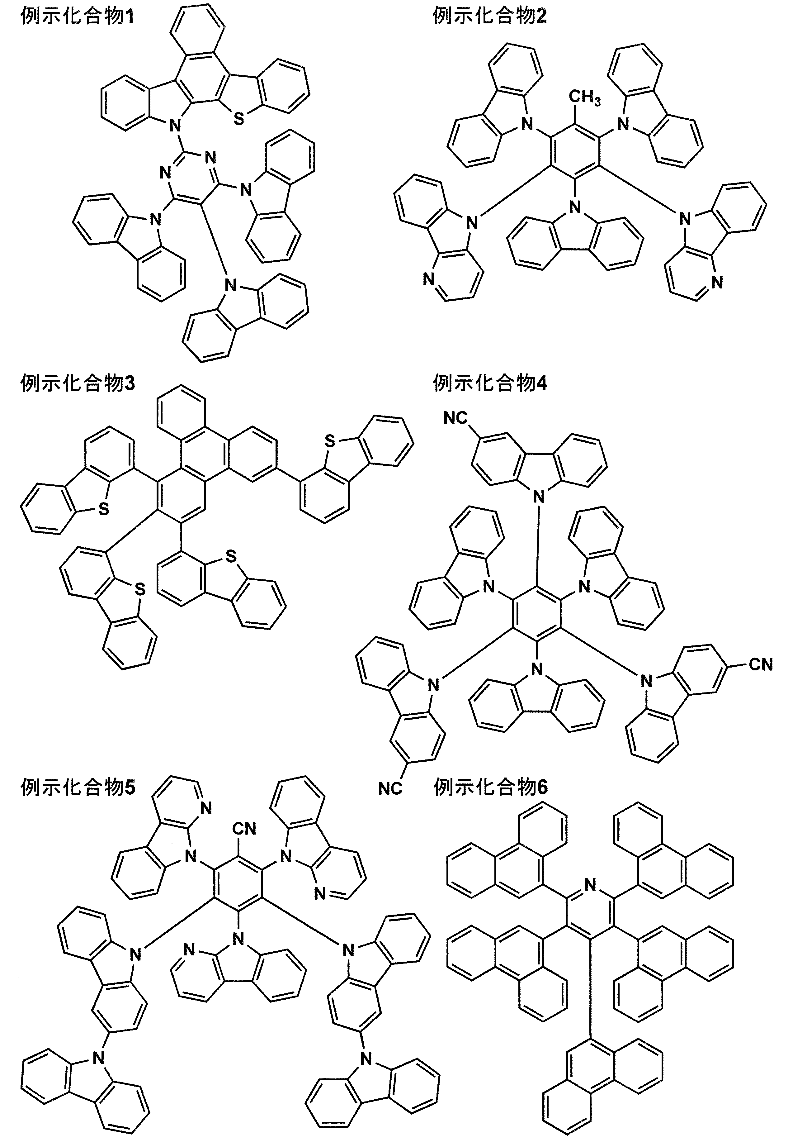
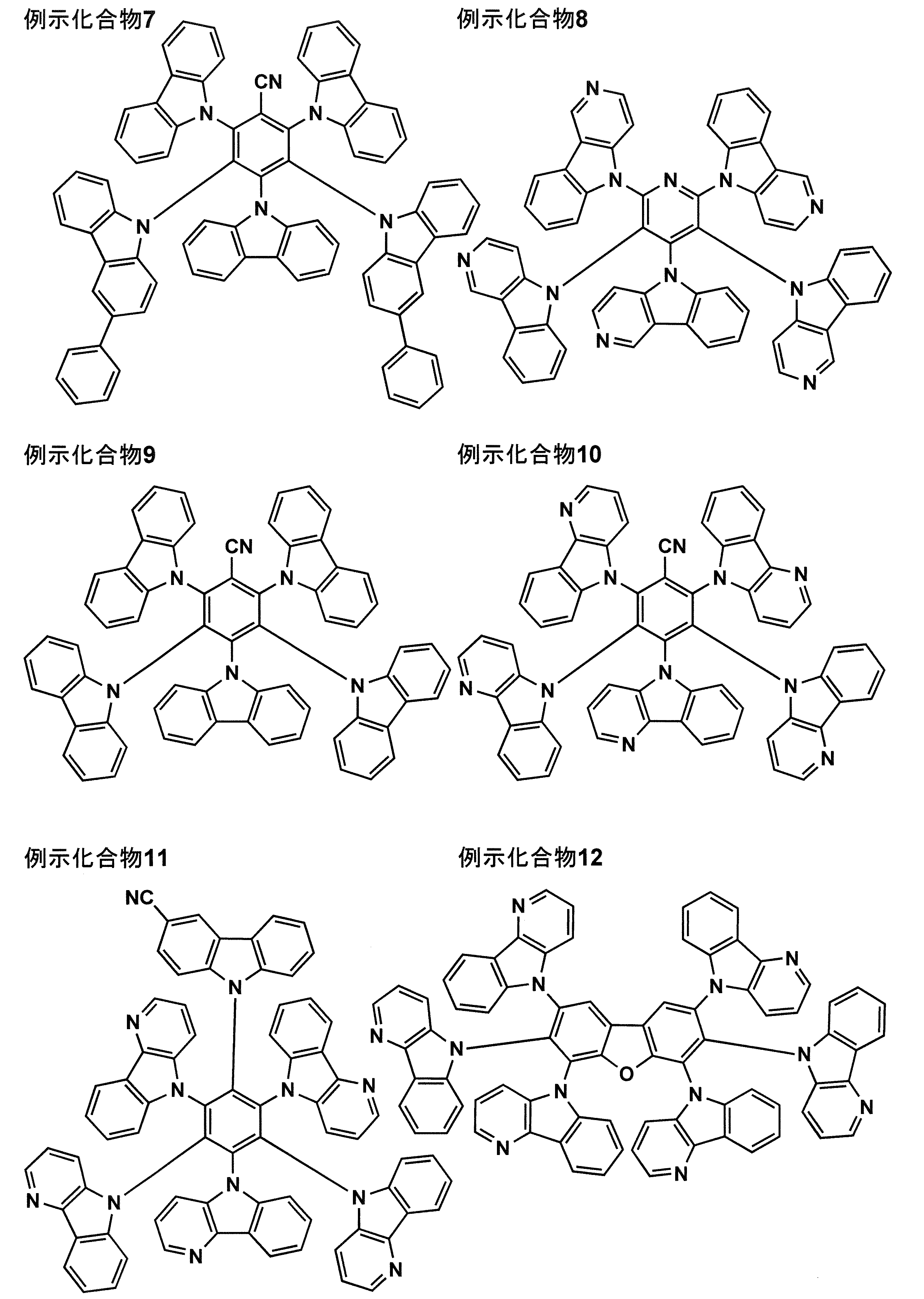


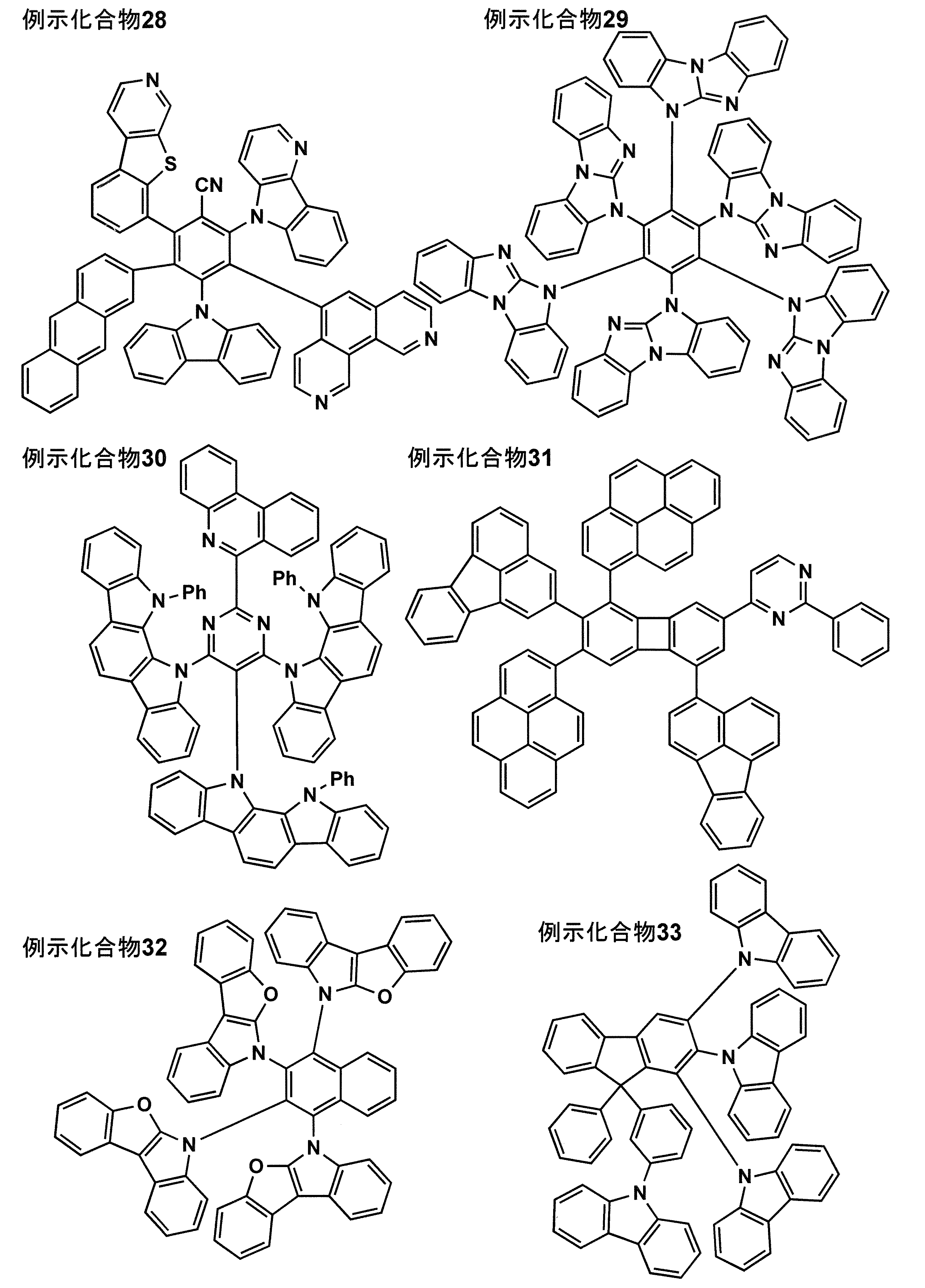


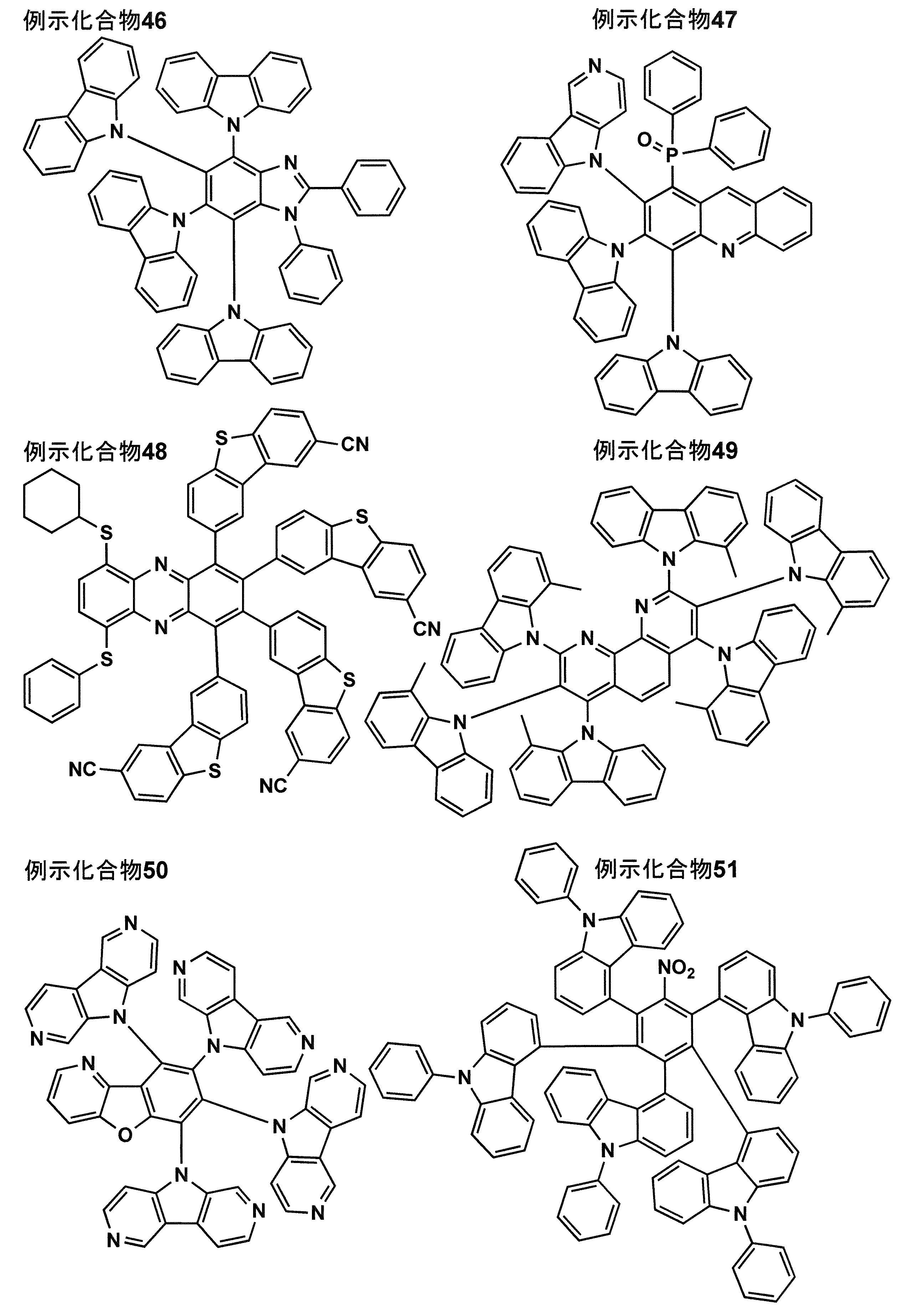
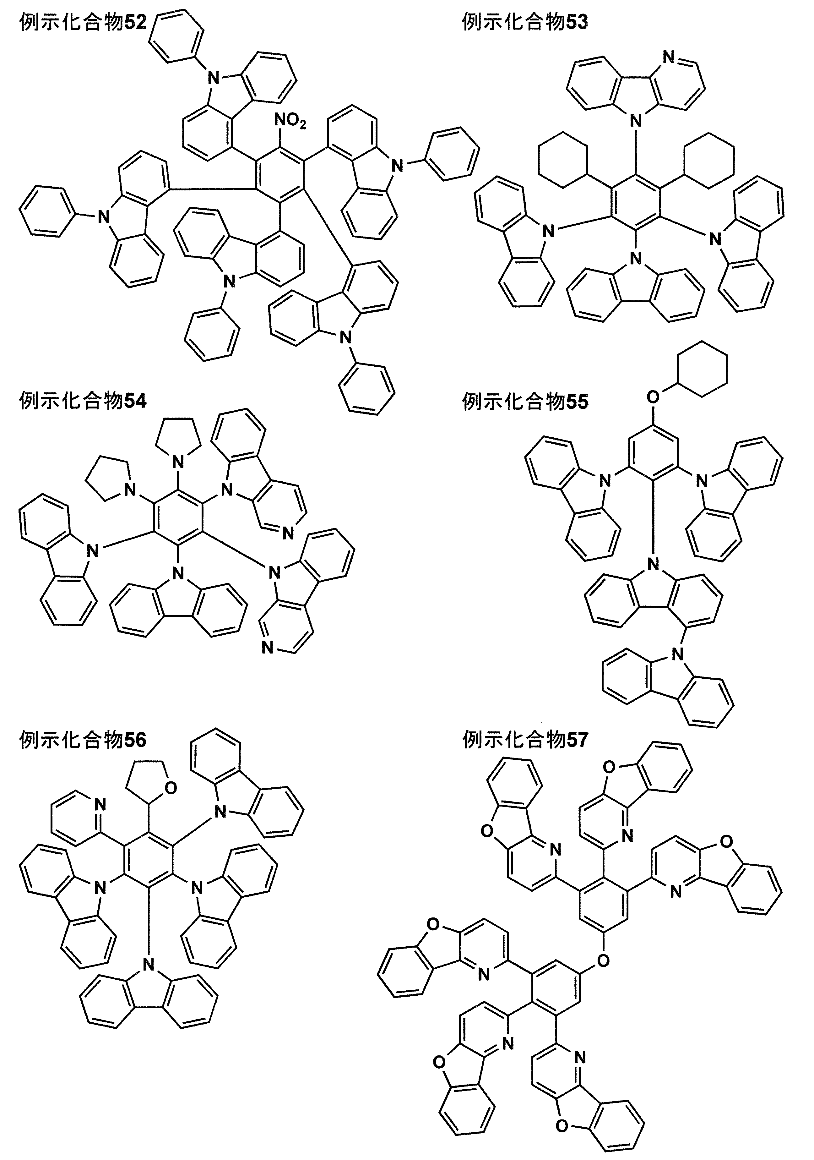
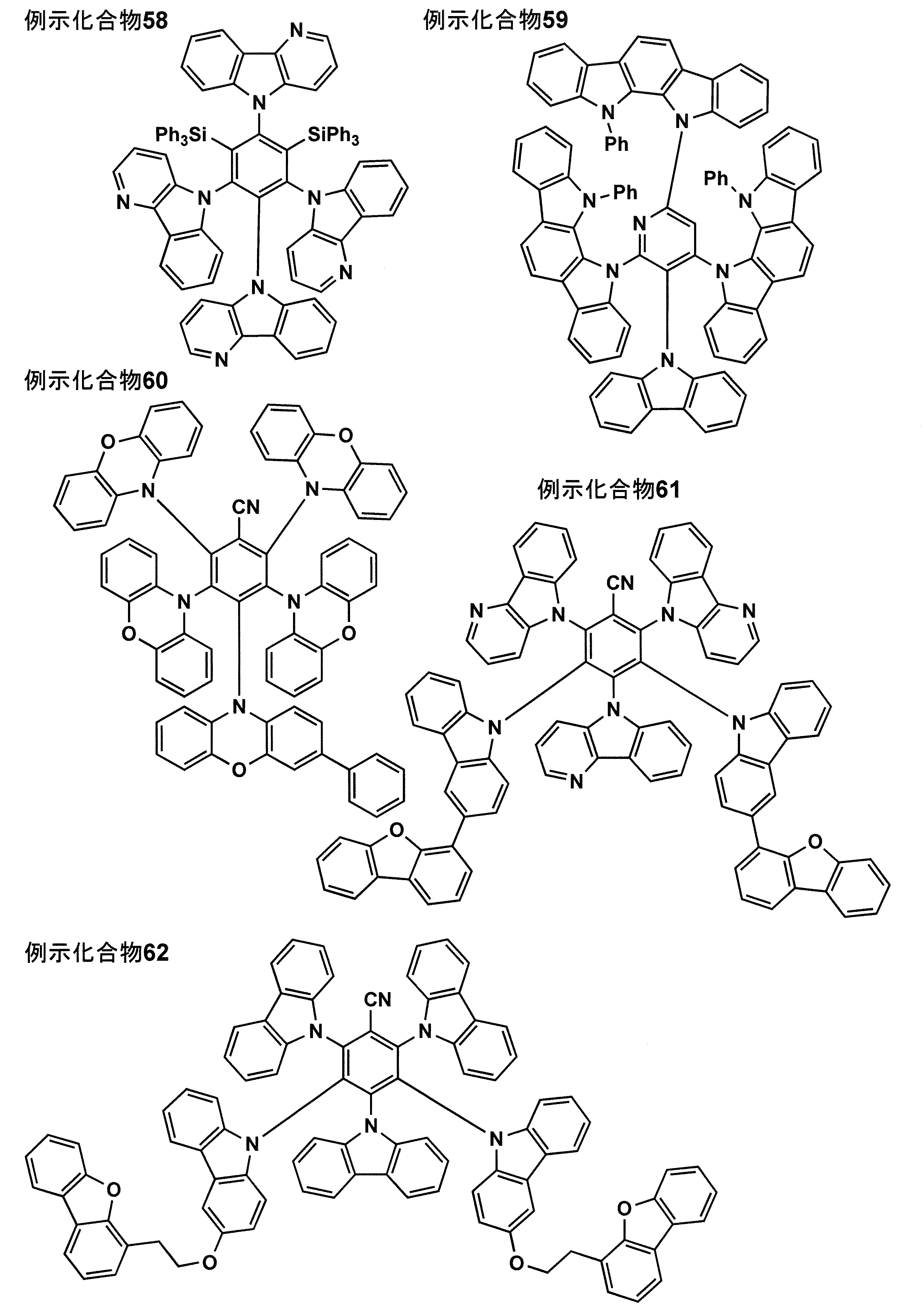
〔2〕機能性膜の形成方法
本発明の機能性膜は、前記多置換構造を有する化合物を、300KにおいてNPTアンサンブルの分子動力学計算で算出した膜密度の値を、前記化合物のみを含有する機能性膜の初期膜密度とし、前記芳香族化合物を、370Kにおいて前記分子動力学計算で算出した膜密度の値を、当該温度下で保存した機能性膜の保存後の膜密度の値としたときに、前記初期膜密度と前記保存後の膜密度の値の差が、初期膜密度に対して1%以下であることを特徴とする。
本発明の機能性膜は、前記多置換構造を有する化合物を、300KにおいてNPTアンサンブルの分子動力学計算で算出した膜密度の値を、前記化合物のみを含有する機能性膜の初期膜密度とし、前記芳香族化合物を、370Kにおいて前記分子動力学計算で算出した膜密度の値を、当該温度下で保存した機能性膜の保存後の膜密度の値としたときに、前記初期膜密度と前記保存後の膜密度の値の差が、初期膜密度に対して1%以下であることを特徴とする。
前記初期膜密度の値の範囲と前記初期膜密度と保存後の膜密度の値の差を、上記値の範囲に制御するには、機能性膜の成膜において、用いる化合物の構造を適宜選択することで達成することができる。
本発明の機能性膜を形成する方法として、スピンコート法、キャスト法、インクジェット法、蒸着法、印刷法等があるが、均質な膜が得られやすく、かつ、ピンホールが生成しにくい等の点から、スピンコート法又は蒸着法が好ましい。特に本発明に係る初期膜密度の範囲を有する成膜や、保存前後の膜密度の変動が制御された成膜をするには、蒸着法を採用することが好ましい。
蒸着系では真空蒸着法、イオンビーム蒸着法、イオンプレーティング法等、スパッタ系ではスパッタリング法、イオンビームスパッタリング法、マグネトロンスパッタリング法等の物理気相成膜法が知られており、さらに、熱CVD法、触媒化学気相成長法(Cat-CVD)、容量結合プラズマCVD法(CCP-CVD)、光CVD法、プラズマCVD法(PE-CVD)、エピタキシャル成長法、原子層成長法等の化学蒸着法等によって成膜することもできる。本発明で、真空蒸着法、イオンビーム蒸着法、イオンプレーティング法等、又はスパッタリング法を採用することが好ましい。
成膜に真空蒸着法を採用する場合、その蒸着条件は使用する化合物の種類等により異なるが、一般にボート加熱温度50~450℃の範囲内、真空度1×10⁻⁶~1×10⁻²Paの範囲内、蒸着速度0.01~50nm/秒の範囲内、基板温度-50~300℃の範囲内で適宜選ぶことが好ましい。
本発明の機能性膜の形成方法としては、一回の真空引きで一貫して真空蒸着法で成膜する方法が好ましいが、途中で取り出して異なる成膜法、例えば、湿式法による形成を行っても構わない。その際の作業環境としては、乾燥不活性ガス雰囲気下で行うことが好ましい。
真空蒸着法は、例えば、抵抗加熱蒸着、高周波誘導加熱蒸着、電子ビーム蒸着、イオンビーム蒸着、プラズマ支援蒸着などが挙げられる。真空蒸着法は真空中で膜にしたい材料を蒸発又は昇華させ、その蒸気が基板(膜をつけたい対象物や箇所)に到達して堆積することで膜を形成する方法である。蒸発材料や基板に、電気的に印加させることもなく、気化した材料がそのまま基板に到達するため、基板のダメージが少なく純度の高い膜が形成できる。真空蒸着法の一例として、イオンアシストデポジション(IAD:Ion Assisted Deposition)法を用いる真空蒸着法であることも好ましい蒸着法として挙げることができる。IAD法は、成膜中にイオンの持つ高い運動エネルギーを作用させて緻密な膜としたり、膜の密着力を高める方法であり、例えばイオンビームによる方法は、イオンソースから照射されるイオン化されたガス分子により被着材料を加速し、基板表面に成膜する方法である。IAD法は、「イオンビームアシスト法」ともいう。詳細は、特開2003-221663号公報や国際公開第2015/030015号等に記載されている。
スパッタリング法は、例えば、マグネトロンカソードスパッタリング、平板マグネトロンスパッタリング、2極AC平板マグネトロンスパッタリング、2極AC回転マグネトロンスパッタリングなど、反応性スパッタ法などが挙げられる。スパッタリング法は、プラズマ等により高いエネルギーをもった粒子を材料(ターゲット)に衝突させて、その衝撃で材料成分をたたき出し、その粒子を基板上に膜を堆積させることで膜を形成する。材料そのものをたたき出しているので、合金の成分がほとんどそのまま基板上に堆積することができる。
イオンプレーティング法はDCイオンプレーティン法、RFイオンプレーティング法などが挙げられる。イオンプレーティング法は、蒸着法とほぼ同じ原理だが、異なるところは、蒸発粒子をプラズマ中を通過させることで、プラスの電荷を帯びさせ、基板にマイナスの電荷を印加して蒸発粒子を引き付けて堆積させ膜を作製する。これにより蒸着法に比べより下層との密着性の強い膜を作ることができる。
本発明の機能性膜の厚さ(複数層積層した場合は全体の厚さ)については、好ましくは、5nm~5μm程度、好ましくは5~200nm程度である。厚さが5nm以上であれば、低電圧駆動、高発光効率、長寿命及び駆動電圧変動耐性を有する機能性層となり、厚さが5μm以下であれば、多層膜自体の膜応力による面変形が発生するのを防止することができる。
〔3〕有機EL素子
本発明の有機EL素子は、少なくとも、一対の電極と一つ又は複数の層とを有する有機エレクトロルミネッセンス素子であって、前記層の少なくとも一層が、本発明の機能性膜を有することを特徴とする。特に、本発明の機能性膜が電荷輸送性膜(後述する正孔輸送層及び電子輸送層)であることが好ましく、隣接した少なくとも2層が本発明の機能性膜であることが、より好ましい。
〔3〕有機EL素子
本発明の有機EL素子は、少なくとも、一対の電極と一つ又は複数の層とを有する有機エレクトロルミネッセンス素子であって、前記層の少なくとも一層が、本発明の機能性膜を有することを特徴とする。特に、本発明の機能性膜が電荷輸送性膜(後述する正孔輸送層及び電子輸送層)であることが好ましく、隣接した少なくとも2層が本発明の機能性膜であることが、より好ましい。
有機EL素子における代表的な素子構成としては、以下の構成を挙げることができるが、これらに限定されるものではない。
(1)陽極/発光層//陰極
(2)陽極/発光層/電子輸送層/陰極
(3)陽極/正孔輸送層/発光層/陰極
(4)陽極/正孔輸送層/発光層/電子輸送層/陰極
(5)陽極/正孔輸送層/発光層/電子輸送層/電子注入層/陰極
(6)陽極/正孔注入層/正孔輸送層/発光層/電子輸送層/陰極
(7)陽極/正孔注入層/正孔輸送層/(電子阻止層/)発光層/(正孔阻止層/)電子輸送層/電子注入層/陰極
上記の中で(7)の構成が好ましく用いられるが、これに限定されるものではない。
(2)陽極/発光層/電子輸送層/陰極
(3)陽極/正孔輸送層/発光層/陰極
(4)陽極/正孔輸送層/発光層/電子輸送層/陰極
(5)陽極/正孔輸送層/発光層/電子輸送層/電子注入層/陰極
(6)陽極/正孔注入層/正孔輸送層/発光層/電子輸送層/陰極
(7)陽極/正孔注入層/正孔輸送層/(電子阻止層/)発光層/(正孔阻止層/)電子輸送層/電子注入層/陰極
上記の中で(7)の構成が好ましく用いられるが、これに限定されるものではない。
本発明では、正孔注入層及び正孔輸送層等を「有機機能層群1」とし、電子輸送層、電子注入層等を「有機機能層群2」という場合がある。
本発明に用いられる発光層は、単層又は複数層で構成されており、発光層が複数の場合は各発光層の間に非発光性の中間層を設けてもよい。
必要に応じて、発光層と陰極との間に正孔阻止層(「正孔障壁層」ともいう。)や電子注入層(「陰極バッファー層」ともいう。)を設けてもよく、また、発光層と陽極との間に電子阻止層(「電子障壁層」ともいう・)や正孔注入層(「陽極バッファー層」ともいう。)を設けてもよい。
本発明に用いられる電子輸送層とは、電子を輸送する機能を有する層であり、広い意味で電子注入層、正孔阻止層も電子輸送層に含まれる。また、複数層で構成されていてもよい。
本発明に用いられる正孔輸送層とは、正孔を輸送する機能を有する層であり、広い意味で正孔注入層、電子阻止層も正孔輸送層に含まれる。また、複数層で構成されていてもよい。
上記の代表的な素子構成において、陽極と陰極を除いた層を「有機層」ともいう。
(タンデム構造)
また、当該有機EL素子は、少なくとも1層の発光層を含む発光ユニットを複数積層した、いわゆるタンデム構造の素子であってもよい。
また、当該有機EL素子は、少なくとも1層の発光層を含む発光ユニットを複数積層した、いわゆるタンデム構造の素子であってもよい。
タンデム構造の代表的な素子構成としては、例えば以下の構成を挙げることができる。
陽極/第1発光ユニット/中間層/第2発光ユニット/中間層/第3発光ユニット/陰極
ここで、上記第1発光ユニット、第2発光ユニット及び第3発光ユニットは全て同じであっても、異なっていてもよい。また二つの発光ユニットが同じであり、残る一つが異なっていてもよい。
ここで、上記第1発光ユニット、第2発光ユニット及び第3発光ユニットは全て同じであっても、異なっていてもよい。また二つの発光ユニットが同じであり、残る一つが異なっていてもよい。
複数の発光ユニットは直接積層されていても、中間層を介して積層されていてもよく、中間層は、一般的に中間電極、中間導電層、電荷発生層、電子引抜層、接続層、中間絶縁層とも呼ばれ、陽極側の隣接層に電子を、陰極側の隣接層に正孔を供給する機能を持った層であれば、公知の材料構成を用いることができる。
中間層に用いられる材料としては、例えば、ITO(インジウムスズ酸化物)、IZO(インジウム・亜鉛酸化物)、ZnO2、TiN、ZrN、HfN、TiOx、VOx、CuI、InN、GaN、CuAlO2、CuGaO2、SrCu2O2、LaB6、RuO2、Al等の導電性無機化合物層や、Au/Bi2O3等の2層膜や、SnO2/Ag/SnO2、ZnO/Ag/ZnO、Bi2O3/Au/Bi2O3、TiO2/TiN/TiO2、TiO2/ZrN/TiO2等の多層膜、またC60等のフラーレン類、オリゴチオフェン等の導電性有機物層、金属フタロシアニン類、無金属フタロシアニン類、金属ポルフィリン類、無金属ポルフィリン類等の導電性有機化合物層等が挙げられるが、本発明はこれらに限定されない。
発光ユニット内の好ましい構成としては、例えば、上記の代表的な素子構成で挙げた(1)~(7)の構成から、陽極と陰極を除いたもの等が挙げられるが、本発明はこれらに限定されない。
タンデム型有機EL素子の具体例としては、例えば、米国特許第6337492号明細書、米国特許第7420203号明細書、米国特許第7473923号明細書、米国特許第6872472号明細書、米国特許第6107734号明細書、米国特許第6337492号明細書、国際公開第2005/009087号、特開2006-228712号公報、特開2006-24791号公報、特開2006-49393号公報、特開2006-49394号公報、特開2006-49396号公報、特開2011-96679号公報、特開2005-340187号公報、特許第4711424号公報、特許第3496681号公報、特許第3884564号公報、特許第4213169号公報、特開2010-192719号公報、特開2009-076929号公報、特開2008-078414号公報、特開2007-059848号公報、特開2003-272860号公報、特開2003-045676号公報、国際公開第2005/094130号等に記載の素子構成や構成材料等が挙げられるが、本発明はこれらに限定されない。
さらに、有機EL素子を構成する各層について説明する。
〔基板〕
有機EL素子に適用可能な基板としては、特に制限はなく、例えば、ガラス、プラスチック等の種類を挙げることができる。
有機EL素子に適用可能な基板としては、特に制限はなく、例えば、ガラス、プラスチック等の種類を挙げることができる。
本発明に用いられる基板は、光透過性であっても、光不透過性であってもよい。本発明に適用可能な基板としては、特に制限されず、例えば、樹脂基板、薄膜金属箔、薄板フレキシブルガラス等が挙げられる。
本発明に適用可能な樹脂基板としては、例えば、ポリエチレンテレフタレート(略称:PET)、ポリエチレンナフタレート(略称:PEN)等のポリエステル、ポリエチレン、ポリプロピレン、セロファン、セルロースジアセテート、セルローストリアセテート(略称:TAC)、セルロースアセテートブチレート、セルロースアセテートプロピオネート(略称:CAP)、セルロースアセテートフタレート、セルロースナイトレート等のセルロースエステル類及びそれらの誘導体、ポリ塩化ビニリデン、ポリビニルアルコール、ポリエチレンビニルアルコール、シンジオタクティックポリスチレン、ポリカーボネート(略称:PC)、ノルボルネン樹脂、ポリメチルペンテン、ポリエーテルケトン、ポリイミド、ポリエーテルスルホン(略称:PES)、ポリフェニレンスルフィド、ポリスルホン類、ポリエーテルイミド、ポリエーテルケトンイミド、ポリアミド、フッ素樹脂、ナイロン、ポリメチルメタクリレート、アクリル及びポリアリレート類、アートン(商品名、JSR社製)及びアペル(商品名、三井化学社製)等のシクロオレフィン系樹脂等を挙げることができる。
これら樹脂基板のうち、コストや入手の容易性の点では、ポリエチレンテレフタレート(略称:PET)、ポリブチレンテレフタレート、ポリエチレンナフタレート(略称:PEN)、ポリカーボネート(略称:PC)等のフィルムが可撓性の樹脂基板として好ましく用いられる。
樹脂基板の厚さとしては、3~200μmの範囲内にある薄膜の樹脂基板であることが好ましいが、より好ましくは10~150μmの範囲内であり、特に好ましくは、20~120μmの範囲内である。
また、本発明用いられる基板として適用可能な薄板ガラスは、湾曲できるほど薄くしたガラス板である。薄板ガラスの厚さは、薄板ガラスが可撓性を示す範囲で適宜設定できる。
薄板ガラスとしては、ソーダ石灰ガラス、バリウム・ストロンチウム含有ガラス、鉛ガラス、アルミノケイ酸ガラス、ホウケイ酸ガラス、バリウムホウケイ酸ガラス、石英等を挙げることができる。薄板ガラスの厚さとしては、例えば、5~300μmの範囲であり、好ましくは20~150μmの範囲である。
また、薄膜金属箔の形成材料としては、例えば、ステンレス、鉄、銅、アルミニウム、マグネシウム、ニッケル、亜鉛、クロム、チタン、モリブテン、シリコン、ゲルマニウム及びタンタルからなる群から選ばれる1種以上の金属又は合金からなるものが挙げられる。薄膜金属箔の厚さは、薄膜金属箔がフレキシビリティーを示す範囲で適宜設定することができ、例えば、10~100μmの範囲内であり、好ましくは20~60μmの範囲内である。
(第1電極:陽極)
有機EL素子を構成する陽極としては、Ag、Au等の金属又は金属を主成分とする合金、CuI、又はインジウム-スズの複合酸化物(ITO)、SnO2及びZnO等の金属酸化物を挙げることができるが、金属又は金属を主成分とする合金であることが好ましく、更に好ましくは、銀又は銀を主成分とする合金である。
有機EL素子を構成する陽極としては、Ag、Au等の金属又は金属を主成分とする合金、CuI、又はインジウム-スズの複合酸化物(ITO)、SnO2及びZnO等の金属酸化物を挙げることができるが、金属又は金属を主成分とする合金であることが好ましく、更に好ましくは、銀又は銀を主成分とする合金である。
透明陽極を、銀を主成分として構成する場合、銀の純度としては、99%以上であることが好ましい。また、銀の安定性を確保するためにパラジウム(Pd)、銅(Cu)及び金(Au)等が添加されていてもよい。
透明陽極は銀を主成分として構成されている層であるが、具体的には、銀単独で形成しても、又は銀(Ag)を含有する合金から構成されていてもよい。そのような合金としては、例えば、銀・マグネシウム(Ag・Mg)、銀・銅(Ag・Cu)、銀・パラジウム(Ag・Pd)、銀・パラジウム・銅(Ag・Pd・Cu)、銀・インジウム(Ag・In)などが挙げられる。
上記陽極を構成する各構成材料の中でも、本発明用いられる有機EL素子を構成する陽極としては、銀を主成分として構成し、厚さが2~20nmの範囲内にある透明陽極であることが好ましいが、更に好ましくは厚さが4~12nmの範囲内である。厚さが20nm以下であれば、透明陽極の吸収成分及び反射成分が低く抑えられ、高い光透過率が維持されるため好ましい。
本発明でいう銀を主成分として構成されている層とは、透明陽極中の銀の含有量が60質量%以上であることをいい、好ましくは銀の含有量が80質量%以上であり、より好ましくは銀の含有量が90質量%以上であり、特に好ましくは銀の含有量が98質量%以上である。また、本発明に係る透明陽極でいう「透明」とは、波長550nmでの光透過率が50%以上であることをいう。
透明陽極においては、銀を主成分として構成されている層が、必要に応じて複数の層に分けて積層された構成であっても良い。
また、本発明においては、陽極が、銀を主成分として構成する透明陽極である場合には、形成する透明陽極の銀膜の均一性を高める観点から、その下部に、下地層を設けることが好ましい。下地層としては、特に制限はないが、窒素原子又は硫黄原子を有する有機化合物を含有する層であることが好ましく、当該下地層上に、透明陽極を形成する方法が好ましい態様である。
〔発光層〕
有機EL素子を構成する発光層は、発光材料としてリン光発光化合物、又は蛍光性化合物を用いることができるが、本発明においては、特に、発光材料としてリン光発光化合物が含有されている構成が好ましい。
有機EL素子を構成する発光層は、発光材料としてリン光発光化合物、又は蛍光性化合物を用いることができるが、本発明においては、特に、発光材料としてリン光発光化合物が含有されている構成が好ましい。
この発光層は、電極又は電子輸送層から注入された電子と、正孔輸送層から注入された正孔とが再結合して発光する層であり、発光する部分は発光層の層内であっても発光層と隣接する層との界面であってもよい。
このような発光層としては、含まれる発光材料が発光要件を満たしていれば、その構成には特に制限はない。また、同一の発光スペクトルや発光極大波長を有する層が複数層あってもよい。この場合、各発光層間には非発光性の中間層を有していることが好ましい。
発光層の厚さの総和は、1~100nmの範囲内にあることが好ましく、より低い駆動電圧を得ることができることから1~30nmの範囲内がさらに好ましい。なお、発光層の厚さの総和とは、発光層間に非発光性の中間層が存在する場合には、当該中間層も含む厚さである。
以上のような発光層は、後述する発光材料やホスト化合物を、例えば、真空蒸着法、スピンコート法、キャスト法、LB法(ラングミュア・ブロジェット、Langmuir Blodgett法)及びインクジェット法等の公知の方法により形成することができる。
また発光層は、複数の発光材料を混合してもよく、リン光発光材料と蛍光発光材料(「蛍光ドーパント」、「蛍光性化合物」ともいう。)とを同一発光層中に混合して用いてもよい。発光層の構成としては、ホスト化合物(「発光ホスト」等ともいう。)及び発光材料(「発光ドーパント化合物」ともいう。)を含有し、発光材料より発光させることが好ましい。
(ホスト化合物)
発光層に含有されるホスト化合物としては、室温(25℃)におけるリン光発光のリン光量子収率が0.1未満の化合物が好ましい。さらにリン光量子収率が0.01未満であることが好ましい。また、発光層に含有される化合物の中で、その層中での体積比が50%以上であることが好ましい。
発光層に含有されるホスト化合物としては、室温(25℃)におけるリン光発光のリン光量子収率が0.1未満の化合物が好ましい。さらにリン光量子収率が0.01未満であることが好ましい。また、発光層に含有される化合物の中で、その層中での体積比が50%以上であることが好ましい。
ホスト化合物としては、公知のホスト化合物を単独で用いてもよく、又は、複数種のホスト化合物を用いてもよい。ホスト化合物を複数種用いることで、電荷の移動を調整することが可能であり、有機電界発光素子を高効率化することができる。また、後述する発光材料を複数種用いることで、異なる発光を混ぜることが可能となり、これにより任意の発光色を得ることができる。
発光層に用いられるホスト化合物としては、従来公知の低分子化合物でも、繰り返し単位をもつ高分子化合物でもよく、ビニル基やエポキシ基のような重合性基を有する低分子化合物(蒸着重合性発光ホスト)でもよい。
本発明に適用可能なホスト化合物としては、例えば、特開2001-257076号公報、同2001-357977号公報、同2002-8860号公報、同2002-43056号公報、同2002-105445号公報、同2002-352957号公報、同2002-231453号公報、同2002-234888号公報、同2002-260861号公報、同2002-305083号公報、米国特許出願公開第2005/0112407号明細書、米国特許出願公開第2009/0030202号明細書、国際公開第2001/039234号、国際公開第2008/056746号、国際公開第2005/089025号、国際公開第2007/063754号、国際公開第2005/030900号、国際公開第2009/086028号、国際公開第2012/023947号、特開2007-254297号公報、欧州特許第2034538号明細書等に記載されている化合物を挙げることができる。
(発光材料)
本発明で用いることのできる発光材料としては、リン光発光性化合物(「リン光性化合物」、「リン光発光材料又はリン光発光ドーパント」ともいう。)及び蛍光発光性化合物(「蛍光性化合物」又は「蛍光発光材料」ともいう。)が挙げられるが、特に、リン光発光性化合物を用いることが、高い発光効率を得ることができる観点から好ましい。
本発明で用いることのできる発光材料としては、リン光発光性化合物(「リン光性化合物」、「リン光発光材料又はリン光発光ドーパント」ともいう。)及び蛍光発光性化合物(「蛍光性化合物」又は「蛍光発光材料」ともいう。)が挙げられるが、特に、リン光発光性化合物を用いることが、高い発光効率を得ることができる観点から好ましい。
〈リン光発光性化合物〉
リン光発光性化合物とは、励起三重項からの発光が観測される化合物であり、具体的には室温(25℃)にてリン光発光する化合物であり、リン光量子収率が25℃において0.01以上の化合物であると定義されるが、好ましいリン光量子収率は0.1以上である。
リン光発光性化合物とは、励起三重項からの発光が観測される化合物であり、具体的には室温(25℃)にてリン光発光する化合物であり、リン光量子収率が25℃において0.01以上の化合物であると定義されるが、好ましいリン光量子収率は0.1以上である。
上記リン光量子収率は、第4版実験化学講座7の分光IIの398頁(1992年版、丸善)に記載の方法により測定できる。溶液中でのリン光量子収率は、種々の溶媒を用いて測定できるが、本発明においてリン光発光性化合物を用いる場合、任意の溶媒のいずれかにおいて、上記リン光量子収率として0.01以上が達成されればよい。
リン光発光性化合物は、一般的な有機EL素子の発光層に使用される公知のものの中から適宜選択して用いることができるが、好ましくは元素の周期表で8~10族の金属を含有する錯体系化合物であり、さらに好ましくはイリジウム化合物、オスミウム化合物、白金化合物(白金錯体系化合物)又は希土類錯体であり、中でも最も好ましいのはイリジウム化合物である。
本発明においては、少なくとも一つの発光層が、二種以上のリン光発光性化合物が含有されていてもよく、発光層におけるリン光発光性化合物の濃度比が発光層の厚さ方向で変化している態様であってもよい。
本発明に使用できる公知のリン光発光性化合物の具体例としては、以下の文献に記載されている化合物等が挙げられる。
Nature 395,151(1998)、Appl.Phys.Lett.78, 1622(2001)、Adv.Mater.19,739(2007)、Chem.Mater.17,3532(2005)、Adv.Mater.17,1059(2005)、国際公開第2009/100991号、国際公開第2008/101842号、国際公開第2003/040257号、米国特許出願公開第2006/835469号明細書、米国特許出願公開第2006/0202194号明細書、米国特許出願公開第2007/0087321号明細書、米国特許出願公開第2005/0244673号明細書等に記載の化合物を挙げることができる。
また、Inorg.Chem.40,1704(2001)、Chem.Mater.16,2480(2004)、Adv.Mater.16,2003(2004)、Angew.Chem.Int.Ed.2006,45,7800、Appl.Phys.Lett.86,153505(2005)、Chem.Lett.34,592(2005)、Chem.Commun.2906(2005)、Inorg.Chem.42,1248(2003)、国際公開第2009/050290号、国際公開第2009/000673号、米国特許第7332232号明細書、米国特許出願公開第2009/0039776号、米国特許第6687266号明細書、米国特許出願公開第2006/0008670号明細書、米国特許出願公開第2008/0015355号明細書、米国特許第7396598号明細書、米国特許出願公開第2003/0138657号明細書、米国特許第7090928号明細書等に記載の化合物を挙げることができる。
また、Angew.Chem.lnt.Ed.47,1(2008)、Chem.Mater.18,5119(2006)、Inorg.Chem.46,4308(2007)、Organometallics 23,3745(2004)、Appl.Phys.Lett.74,1361(1999)、国際公開第2006/056418号、国際公開第2005/123873号、国際公開第2006/082742号、米国特許出願公開第2005/0260441号明細書、米国特許第7534505号明細書、米国特許出願公開第2007/0190359号明細書、米国特許第7338722号明細書、米国特許第7279704号明細書、米国特許出願公開第2006/103874号明細書等に記載の化合物も挙げることができる。
さらには、国際公開第2005/076380号、国際公開第2008/140115号、国際公開第2011/134013号、国際公開第2010/086089号、国際公開第2012/020327号、国際公開第2011/051404号、国際公開第2011/073149号、特開2009-114086号公報、特開2003-81988号公報、特開2002-363552号公報等に記載の化合物も挙げることができる。
本発明においては、好ましいリン光発光性化合物としてはIrを中心金属に有する有機金属錯体が挙げられる。さらに好ましくは、金属-炭素結合、金属-窒素結合、金属-酸素結合、金属-硫黄結合の少なくとも一つの配位様式を含む錯体が好ましい。
上記説明したリン光発光性化合物(「リン光発光性金属錯体」ともいう。)は、例えば、Organic Letter誌、vol3、No.16、2579~2581頁(2001)、Inorganic Chemistry,第30巻、第8号、1685~1687頁(1991年)、J.Am.Chem.Soc.,123巻、4304頁(2001年)、Inorganic Chemistry,第40巻、第7号、1704~1711頁(2001年)、Inorganic Chemistry,第41巻、第12号、3055~3066頁(2002年)、New Journal of Chemistry.,第26巻、1171頁(2002年)、European Journal of
Organic Chemistry,第4巻、695~709頁(2004年)、さらにこれらの文献中に記載されている参考文献等に開示されている方法を適用することにより合成することができる。
Organic Chemistry,第4巻、695~709頁(2004年)、さらにこれらの文献中に記載されている参考文献等に開示されている方法を適用することにより合成することができる。
〈蛍光発光性化合物〉
蛍光発光性化合物としては、クマリン系色素、ピラン系色素、シアニン系色素、クロコニウム系色素、スクアリウム系色素、オキソベンツアントラセン系色素、フルオレセイン系色素、ローダミン系色素、ピリリウム系色素、ペリレン系色素、スチルベン系色素、ポリチオフェン系色素又は希土類錯体系蛍光体等が挙げられる。
蛍光発光性化合物としては、クマリン系色素、ピラン系色素、シアニン系色素、クロコニウム系色素、スクアリウム系色素、オキソベンツアントラセン系色素、フルオレセイン系色素、ローダミン系色素、ピリリウム系色素、ペリレン系色素、スチルベン系色素、ポリチオフェン系色素又は希土類錯体系蛍光体等が挙げられる。
また、近年、有機EL素子用のホスト材料又は発光材料(例えば青色発光する熱活性型遅延蛍光(TADF:thermally activated delayed fluorescence)化合物)として、カルバゾール環基を有するベンゾニトリル誘導体の使用が提案されている。なお、ベンゾニトリル骨格を有し、青色発光性のTADF化合物としては、2CzPN(ジカルバゾリルフタロニトリル:4,5-di(9H-carbazol-9-yl)phthalonitrile)、4CzIPN(テトラカルバゾリルイソフタロニトリル:2,4,5,6-tetra(9H-carbazol-9-yl)isophthalonitrile)及び5CzBN(ペンタカルバゾリルベンゾニトリル:2,3,4,5,6-pentakis(carbazol-9-yl)benzonitrile)等が知られており、好適に用いることができる。
〔有機機能層群〕
次いで、有機機能層群1及び2を構成する各層について、電荷注入層、正孔輸送層、電子輸送層及び阻止層の順に説明する。
次いで、有機機能層群1及び2を構成する各層について、電荷注入層、正孔輸送層、電子輸送層及び阻止層の順に説明する。
(電荷注入層)
電荷注入層は、駆動電圧低下や発光輝度向上のために、電極と発光層の間に設けられる層のことで、「有機EL素子とその工業化最前線(1998年11月30日エヌ・ティー・エス社発行)」の第2編第2章「電極材料」(123~166頁)にその詳細が記載されており、正孔注入層と電子注入層とがある。
電荷注入層は、駆動電圧低下や発光輝度向上のために、電極と発光層の間に設けられる層のことで、「有機EL素子とその工業化最前線(1998年11月30日エヌ・ティー・エス社発行)」の第2編第2章「電極材料」(123~166頁)にその詳細が記載されており、正孔注入層と電子注入層とがある。
電荷注入層としては、一般には、正孔注入層であれば、陽極と発光層又は正孔輸送層との間、電子注入層であれば陰極と発光層又は電子輸送層との間に存在させることができるが、本発明においては、透明電極に隣接して電荷注入層を配置させることを特徴とする。また、中間電極で用いられる場合は、隣接する電子注入層及び正孔注入層の少なくとも一方が、本発明の要件を満たしていれば良い。
正孔注入層は、駆動電圧低下や発光輝度向上のために、透明電極である陽極に隣接して配置される層であり、「有機EL素子とその工業化最前線(1998年11月30日エヌ・ティー・エス社発行)」の第2編第2章「電極材料」(123~166頁)に詳細に記載されている。
正孔注入層は、特開平9-45479号公報、同9-260062号公報、同8-288069号公報等にもその詳細が記載されており、正孔注入層に用いられる材料としては、例えば、ポルフィリン誘導体、フタロシアニン誘導体、オキサゾール誘導体、オキサジアゾール誘導体、トリアゾール誘導体、イミダゾール誘導体、ピラゾリン誘導体、ピラゾロン誘導体、フェニレンジアミン誘導体、ヒドラゾン誘導体、スチルベン誘導体、ポリアリールアルカン誘導体、トリアリールアミン誘導体、カルバゾール誘導体、インドロカルバゾール誘導体、イソインドール誘導体、アントラセンやナフタレン等のアセン系誘導体、フルオレン誘導体、フルオレノン誘導体、及びポリビニルカルバゾール、芳香族アミンを主鎖又は側鎖に導入した高分子材料又はオリゴマー、ポリシラン、導電性ポリマー又はオリゴマー(例えば、PEDOT(ポリエチレンジオキシチオフェン):PSS(ポリスチレンスルホン酸)、アニリン系共重合体、ポリアニリン、ポリチオフェン等)等が挙げられる。
トリアリールアミン誘導体としては、α-NPD(4,4′-ビス〔N-(1-ナフチル)-N-フェニルアミノ〕ビフェニル)に代表されるベンジジン型や、MTDATA(4,4′,4″-トリス〔N-(3-メチルフェニル)-N-フェニルアミノ〕トリフェニルアミン)に代表されるスターバースト型、トリアリールアミン連結コア部にフルオレンやアントラセンを有する化合物等が挙げられる。
また、特表2003-519432号公報や特開2006-135145号公報等に記載されているようなヘキサアザトリフェニレン誘導体も同様に正孔輸送材料として用いることができる。
電子注入層は、駆動電圧低下や発光輝度向上のために、陰極と発光層との間に設けられる層のことであり、陰極が本発明に係る透明電極で構成されている場合には、当該透明電極に隣接して設けられ、「有機EL素子とその工業化最前線(1998年11月30日エヌ・ティー・エス社発行)」の第2編第2章「電極材料」(123~166頁)に詳細に記載されている。
電子注入層は、特開平6-325871号公報、同9-17574号公報、同10-74586号公報等にもその詳細が記載されており、電子注入層に好ましく用いられる材料の具体例としては、ストロンチウムやアルミニウム等に代表される金属、フッ化リチウム、フッ化ナトリウム、フッ化カリウム等に代表されるアルカリ金属化合物、フッ化マグネシウム、フッ化カルシウム等に代表されるアルカリ金属ハライド層、フッ化マグネシウムに代表されるアルカリ土類金属化合物層、酸化モリブデン、酸化アルミニウム等に代表される金属酸化物、リチウム8-ヒドロキシキノレート(Liq)等に代表される金属錯体等が挙げられる。また、本発明における透明電極が陰極の場合は、金属錯体等の有機材料が特に好適に用いられる。電子注入層はごく薄い膜であることが望ましく、構成材料にもよるが、その層厚は1nm~10μmの範囲が好ましい。
(正孔輸送層)
正孔輸送層とは正孔を輸送する機能を有する正孔輸送材料からなり、広い意味で正孔注入層及び電子阻止層も正孔輸送層の機能を有する。正孔輸送層は単層又は複数層設けることができる。
正孔輸送層とは正孔を輸送する機能を有する正孔輸送材料からなり、広い意味で正孔注入層及び電子阻止層も正孔輸送層の機能を有する。正孔輸送層は単層又は複数層設けることができる。
正孔輸送材料としては、正孔の注入又は輸送、電子の障壁性のいずれかを有するものであり、有機物、無機物のいずれであってもよい。例えば、トリアゾール誘導体、オキサジアゾール誘導体、イミダゾール誘導体、ポリアリールアルカン誘導体、ピラゾリン誘導体、ピラゾロン誘導体、フェニレンジアミン誘導体、アリールアミン誘導体、アミノ置換カルコン誘導体、オキサゾール誘導体、スチリルアントラセン誘導体、フルオレノン誘導体、ヒドラゾン誘導体、スチルベン誘導体、シラザン誘導体、アニリン系共重合体、導電性高分子オリゴマー及びチオフェンオリゴマー等が挙げられる。
正孔輸送材料としては、上記のものを使用することができるが、ポルフィリン化合物、芳香族第3級アミン化合物及びスチリルアミン化合物を用いることができ、特に芳香族第3級アミン化合物を用いることが好ましい。
芳香族第3級アミン化合物及びスチリルアミン化合物の代表例としては、N,N,N′,N′-テトラフェニル-4,4′-ジアミノフェニル、N,N′-ジフェニル-N,N′-ビス(3-メチルフェニル)-〔1,1′-ビフェニル〕-4,4′-ジアミン(略称:TPD)、2,2-ビス(4-ジ-p-トリルアミノフェニル)プロパン、1,1-ビス(4-ジ-p-トリルアミノフェニル)シクロヘキサン、N,N,N′,N′-テトラ-p-トリル-4,4′-ジアミノビフェニル、1,1-ビス(4-ジ-p-トリルアミノフェニル)-4-フェニルシクロヘキサン、ビス(4-ジメチルアミノ-2-メチルフェニル)フェニルメタン、ビス(4-ジ-p-トリルアミノフェニル)フェニルメタン、N,N′-ジフェニル-N,N′-ジ(4-メトキシフェニル)-4,4′-ジアミノビフェニル、N,N,N′,N′-テトラフェニル-4,4′-ジアミノジフェニルエーテル、4,4′-ビス(ジフェニルアミノ)クオードリフェニル、N,N,N-トリ(p-トリル)アミン、4-(ジ-p-トリルアミノ)-4′-〔4-(ジ-p-トリルアミノ)スチリル〕スチルベン、4-N,N-ジフェニルアミノ-(2-ジフェニルビニル)ベンゼン、3-メトキシ-4′-N,N-ジフェニルアミノスチルベンゼン及びN-フェニルカルバゾール等が挙げられる。
正孔輸送層は、上記正孔輸送材料を、例えば、真空蒸着法、スピンコート法、キャスト法、インクジェット法を含む印刷法及びLB法(ラングミュア・ブロジェット、Langmuir Blodgett法)等の公知の方法により、薄膜化することにより形成することができる。正孔輸送層の層厚については特に制限はないが、通常は5nm~5μm程度、好ましくは5~200nmの範囲である。この正孔輸送層は、上記材料の一種又は二種以上からなる一層構造であってもよい。
また、正孔輸送層の材料に不純物をドープすることにより、p性を高くすることもできる。その例としては、特開平4-297076号公報、特開2000-196140号公報、同2001-102175号公報及びJ.Appl.Phys.,95,5773(2004)等に記載されたものが挙げられる。
このように、正孔輸送層のp性を高くすると、より低消費電力の素子を作製することができるため好ましい。
(電子輸送層)
電子輸送層は、電子を輸送する機能を有する材料から構成され、広い意味で電子注入層、正孔阻止層も電子輸送層に含まれる。電子輸送層は、単層構造又は複数層の積層構造として設けることができる。
電子輸送層は、電子を輸送する機能を有する材料から構成され、広い意味で電子注入層、正孔阻止層も電子輸送層に含まれる。電子輸送層は、単層構造又は複数層の積層構造として設けることができる。
単層構造の電子輸送層及び積層構造の電子輸送層において、発光層に隣接する層部分を構成する電子輸送材料(正孔阻止材料を兼ねる)としては、カソードより注入された電子を発光層に伝達する機能を有していれば良い。このような材料としては、従来公知の化合物の中から任意のものを選択して用いることができる。例えば、ニトロ置換フルオレン誘導体、ジフェニルキノン誘導体、チオピランジオキシド誘導体、カルボジイミド、フレオレニリデンメタン誘導体、アントラキノジメタン、アントロン誘導体及びオキサジアゾール誘導体等が挙げられる。さらに、上記オキサジアゾール誘導体において、オキサジアゾール環の酸素原子を硫黄原子に置換したチアジアゾール誘導体、電子吸引基として知られているキノキサリン環を有するキノキサリン誘導体も、電子輸送層の材料として用いることができる。さらにこれらの材料を高分子鎖に導入した高分子材料又はこれらの材料を高分子の主鎖とした高分子材料を用いることもできる。
また、8-キノリノール誘導体の金属錯体、例えば、トリス(8-キノリノール)アルミニウム(略称:Alq3)、トリス(5,7-ジクロロ-8-キノリノール)アルミニウム、トリス(5,7-ジブロモ-8-キノリノール)アルミニウム、トリス(2-メチル-8-キノリノール)アルミニウム、トリス(5-メチル-8-キノリノール)アルミニウム、ビス(8-キノリノール)亜鉛(略称:Znq)等及びこれらの金属錯体の中心金属がIn、Mg、Cu、Ca、Sn、Ga又はPbに置き替わった金属錯体も、電子輸送層の材料として用いることができる。
電子輸送層は、上記材料を、例えば、真空蒸着法、スピンコート法、キャスト法、インクジェット法を含む印刷法及びLB法等の公知の方法により、薄膜化することで形成することができる。電子輸送層の層厚については特に制限はないが、通常は5nm~5μm程度、好ましくは5~200nmの範囲内である。電子輸送層は上記材料の1種又は2種以上からなる単一構造であってもよい。
(阻止層)
阻止層としては、正孔阻止層及び電子阻止層が挙げられ、上記説明した有機機能層ユニット3の各構成層の他に、必要に応じて設けられる層である。例えば、特開平11-204258号公報、同11-204359号公報、及び「有機EL素子とその工業化最前線(1998年11月30日エヌ・ティー・エス社発行)」の237頁等に記載されている正孔阻止(ホールブロック)層等を挙げることができる。
阻止層としては、正孔阻止層及び電子阻止層が挙げられ、上記説明した有機機能層ユニット3の各構成層の他に、必要に応じて設けられる層である。例えば、特開平11-204258号公報、同11-204359号公報、及び「有機EL素子とその工業化最前線(1998年11月30日エヌ・ティー・エス社発行)」の237頁等に記載されている正孔阻止(ホールブロック)層等を挙げることができる。
正孔阻止層とは、広い意味では、電子輸送層の機能を有する。正孔阻止層は、電子を輸送する機能を有しつつ正孔を輸送する能力が著しく小さい正孔阻止材料からなり、電子を輸送しつつ正孔を阻止することで電子と正孔の再結合確率を向上させることができる。また、電子輸送層の構成を必要に応じて、正孔阻止層として用いることができる。正孔阻止層は、発光層に隣接して設けられていることが好ましい。
一方、電子阻止層とは、広い意味では、正孔輸送層の機能を有する。電子阻止層は、正孔を輸送する機能を有しつつ、電子を輸送する能力が著しく小さい材料からなり、正孔を輸送しつつ電子を阻止することで電子と正孔の再結合確率を向上させることができる。また、正孔輸送層の構成を必要に応じて電子阻止層として用いることができる。本発明に適用する正孔阻止層の層厚としては、好ましくは3~100nmの範囲であり、さらに好ましくは5~30nmの範囲である。
〔第2電極:陰極〕
陰極は、有機機能層群や発光層に正孔を供給するために機能する電極膜であり、金属、合金、有機又は無機の導電性化合物若しくはこれらの混合物が用いられる。具体的には、金、アルミニウム、銀、マグネシウム、リチウム、マグネシウム/銅混合物、マグネシウム/銀混合物、マグネシウム/アルミニウム混合物、マグネシウム/インジウム混合物、インジウム、リチウム/アルミニウム混合物、希土類金属、ITO、ZnO、TiO2及びSnO2等の酸化物半導体などが挙げられる。
陰極は、有機機能層群や発光層に正孔を供給するために機能する電極膜であり、金属、合金、有機又は無機の導電性化合物若しくはこれらの混合物が用いられる。具体的には、金、アルミニウム、銀、マグネシウム、リチウム、マグネシウム/銅混合物、マグネシウム/銀混合物、マグネシウム/アルミニウム混合物、マグネシウム/インジウム混合物、インジウム、リチウム/アルミニウム混合物、希土類金属、ITO、ZnO、TiO2及びSnO2等の酸化物半導体などが挙げられる。
陰極は、これらの導電性材料やその分散液をスピンコート法、キャスト法、インクジェット法、蒸着法、印刷法等の方法により薄膜を形成させて作製することができる。また、第2電極としてのシート抵抗は、数百Ω/sq.以下が好ましく、膜厚は通常5nm~5μm、好ましくは5~200nmの範囲で選ばれる。
なお、有機EL素子が、陰極側からも発光光Lを取り出す、両面発光型の場合には、光透過性の良好な陰極を選択して構成すればよい。
〔封止部材〕
有機EL素子を封止するのに用いられる封止手段としては、例えば、フレキシブル封止部材と、陰極及び透明基板とを封止用接着剤で接着する方法を挙げることができる。
有機EL素子を封止するのに用いられる封止手段としては、例えば、フレキシブル封止部材と、陰極及び透明基板とを封止用接着剤で接着する方法を挙げることができる。
封止部材としては、有機EL素子の表示領域を覆うように配置されていればよく、凹板状でも、平板状でもよい。また透明性及び電気絶縁性は特に限定されない。
具体的には、フレキシブル性を備えた薄膜ガラス板、ポリマー板、フィルム、金属フィルム(金属箔)等が挙げられる。ガラス板としては、特にソーダ石灰ガラス、バリウム・ストロンチウム含有ガラス、鉛ガラス、アルミノケイ酸ガラス、ホウケイ酸ガラス、バリウムホウケイ酸ガラス、石英等を挙げることができる。また、ポリマー板としては、ポリカーボネート、アクリル、ポリエチレンテレフタレート、ポリエーテルサルファイド、ポリサルフォン等を挙げることができる。金属フィルムとしては、ステンレス、鉄、銅、アルミニウム、マグネシウム、ニッケル、亜鉛、クロム、チタン、モリブテン、シリコン、ゲルマニウム及びタンタルからなる群から選ばれる1種以上の金属又は合金が挙げられる。
本発明においては、封止部材としては、有機EL素子を薄膜化することできる観点から、ポリマーフィルム及び金属フィルムを好ましく使用することができる。さらに、ポリマーフィルムは、JIS K 7129-1992に準拠した方法で測定された温度25±0.5℃、相対湿度90±2%RHにおける水蒸気透過度が、1×10⁻³g/m2・24h以下であることが好ましく、さらには、JIS K 7126-1987に準拠した方法で測定された酸素透過度が、1×10⁻³mL/m2・24h・atom(1atomは、1.01325×105Paである)以下であって、温度25±0.5℃、相対湿度90±2%RHにおける水蒸気透過度が、1×10-3g/m2・24h以下であることが好ましい。
封止部材と有機EL素子の表示領域(発光領域)との間隙には、気相及び液相では窒素、アルゴン等の不活性気体やフッ化炭化水素、シリコーンオイルのような不活性液体を注入することもできる。また、封止部材と有機EL素子の表示領域との間隙を真空とすることや、間隙に吸湿性化合物を封入することもできる。
また、有機EL素子における発光機能層ユニットを完全に覆い、かつ有機EL素子における第1電極である陽極(3)と、第2電極である陰極(6)の端子部分を露出させる状態で、透明基板上に封止膜を設けることもできる。
このような封止膜は、無機材料や有機材料を用いて構成され、特に、水分や酸素等の浸入を抑制する機能を有する材料、例えば、酸化ケイ素、二酸化ケイ素、窒化ケイ素等の無機材料が用いられる。さらに封止膜の脆弱性を改良するために、これら無機材料からなる膜とともに、有機材料からなる膜を用いて積層構造としても良い。
これらの封止膜の形成方法については、特に限定はなく、例えば、真空蒸着法、スパッタリング法、反応性スパッタリング法、分子線エピタキシー法、クラスターイオンビーム法、イオンプレーティング法、プラズマ重合法、大気圧プラズマ重合法、プラズマCVD法、レーザーCVD法、熱CVD法、コーティング法等を用いることができる。
以上のような封止材は、有機EL素子における第1電極である陽極(3)と、第2電極である陰極(6)の端子部分を露出させるとともに、少なくとも発光機能層を覆う状態で設けられている。
〔有機EL素子の製造方法〕
有機EL素子の製造方法としては、透明基材上に、陽極、有機機能層群1、発光層、有機機能層群2及び陰極を積層して積層体を形成する。
有機EL素子の製造方法としては、透明基材上に、陽極、有機機能層群1、発光層、有機機能層群2及び陰極を積層して積層体を形成する。
まず、透明基材を準備し、該透明基材上に、所望の電極物質、例えば、陽極用物質からなる薄膜を1μm以下、好ましくは10~200nmの範囲内の膜厚になるように、蒸着やスパッタリング等の方法により形成させ、陽極を形成する。同時に、陽極端部に、外部電源と接続する接続電極部を形成する。
次に、この上に、有機機能層群1を構成する正孔注入層及び正孔輸送層、発光層、有機機能層群2を構成する電子輸送層等を順に積層する。
これらの各層の形成は、スピンコート法、キャスト法、インクジェット法、蒸着法、印刷法等があるが、均質な層が得られやすく、かつ、ピンホールが生成しにくい等の点から、真空蒸着法が特に好ましい。更に、層ごとに異なる形成法を適用しても良い。これらの各層の形成に蒸着法を採用する場合、その蒸着条件は使用する化合物の種類等により異なるが、一般にボート加熱温度50~450℃、真空度1×10⁻⁶~1×10⁻²Pa、蒸着速度0.01~50nm/秒、基板温度-50~300℃、層厚0.1~5μmの範囲内で、各条件を適宜選択することが望ましい。
以上のようにして有機機能層群2を形成した後、この上部に陰極をスピンコート法、キャスト法、インクジェット法、蒸着法、印刷法などの適宜の形成法によって形成する。この際、陰極は、有機機能層群によって陽極に対して絶縁状態を保ちつつ、有機機能層群の上方から透明基板の周縁に端子部分を引き出した形状にパターン形成する。
陰極の形成後、これら透明基材、陽極、有機機能層群、発光層及び陰極を封止材で封止する。すなわち、陽極及び陰極の端子部分を露出させた状態で、透明基材上に、少なくとも有機機能層群を覆う封止材を設ける。
有機EL素子は、電子機器、例えば、表示装置、ディスプレイ、各種発光装置として用いることができる。発光装置として、例えば、照明装置(家庭用照明、車内照明)、時計や液晶用バックライト、看板広告、信号機、光記憶媒体の光源、電子写真複写機の光源、光通信処理機の光源、光センサーの光源等が挙げられるがこれに限定するものではないが、特に液晶表示装置のバックライト、照明用光源としての用途に有効に用いることができる。
[照明装置の一態様]
本発明の有機EL素子を具備した、照明装置の一態様について説明する。
本発明の有機EL素子を具備した、照明装置の一態様について説明する。
本発明の有機EL素子の非発光面をガラスケースで覆い、厚さ300μmのガラス基板を封止用基板として用いて、周囲にシール材として、エポキシ系光硬化型接着剤(東亞合成社製ラックストラックLC0629B)を適用し、これを陰極上に重ねて透明支持基板と密着させ、ガラス基板側からUV光を照射して、硬化させて、封止し、図1及び図2に示すような照明装置を形成することができる。
図1は、照明装置の概略図を示し、本発明の有機EL素子(照明装置内の有機EL素子101)はガラスカバー102で覆われている(なお、ガラスカバーでの封止作業は、照明装置内の有機EL素子101を大気に接触させることなく窒素雰囲気下のグローブボックス(純度99.999%以上の高純度窒素ガスの雰囲気下)で行った)。
図2は、照明装置の断面図を示し、105は陰極、106は有機層、107は透明電極付きガラス基板を示す。なお、ガラスカバー102内には窒素ガス108が充填され、捕水剤109が設けられている。
本発明の有機EL素子を用いることにより、発光効率が向上した照明装置が得られる。
以下、実施例を挙げて本発明を具体的に説明するが、本発明はこれらに限定されるものではない。なお、実施例において「部」又は「%」の表示を用いるが、特に断りがない限り「質量部」又は「質量%」を表す。
まず、実施例で用いる化合物を以下の手順にて合成した。
<例示化合物7の合成>
下記スキームにより合成した。
下記スキームにより合成した。

THF(テトラヒドロフラン)(42mL)中にカルバゾール(6.47g、38.68mol)を溶かしNaH(1.68g、42.0mol)を加え30分撹拌した。その後2,3,4,5,6-ペンタフルオロベンゾニトリル(1.32g、10.8mol)を溶液中に加え、加熱還流させながら5時間撹拌した。反応液に水を加え、析出物を濾取した。これを再結晶して中間体を6.51g得た。
次に、NMP:N-メチルピロリドン(42mL)中に3-フェニル-9H-カルバゾール(5.96g、24.5mol)を溶かしNaH(0.98g、24.5mol)を加え30分撹拌した。その後、中間体(6.51g、10.2mol)を溶液中に加え、120℃で5時間加熱撹拌した。反応液に水を加え、析出物を濾取した。これを再結晶して目的の例示化合物(7)9.93gを得た。
<例示化合物10の合成>
主に原材料のカルバゾールを変更した以外は上記と同様にして、下記スキームにより合成した。
主に原材料のカルバゾールを変更した以外は上記と同様にして、下記スキームにより合成した。
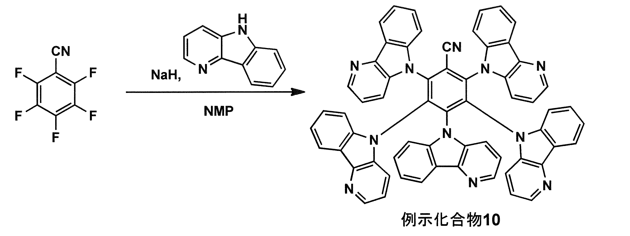
NMP(42mL)中にカルボリン(10.9g、64.6mol)を溶かしNaH(2.80g、70.0mol)を加え30分撹拌した。その後2,3,4,5,6-ペンタフルオロベンゾニトリル(1.32g、10.8mol)を溶液中に加え、120℃で5時間加熱撹拌した。反応液に水を加え、析出物を濾取した。これを再結晶して目的の例示化合物(10)9.20gを得た。
<例示化合物15の合成>
主に原材料のカルバゾールを変更した以外は上記と同様にして、例示化合物15を下記スキームにより合成した。
主に原材料のカルバゾールを変更した以外は上記と同様にして、例示化合物15を下記スキームにより合成した。

ジオキサン(50mL)中に4-シアノフェニルボロン酸(1.2g,4.1mmol)とペンタフルオロヨードベンゼン(0.6g,4.1mmol)を溶かしてPd2(dba)3(0.2g,0.2mmol),K2CO3(1.7g,12.2mmol)、S-Phos(0.3g,0.8mmol)を加えて110℃で6時間攪拌した。反応液に水を加え、析出物を濾取した。これを再結晶して中間体1.07gを得た。
次にTHF(42mL)中に5H-ピリド[3,2-b]インドール(4.0g,23.9mmol)を溶かしNaH(1.0g,23.9mmol)を加え30分撹拌した。その後中間体(1.07g,4.0mmol)を溶液中に加え、70℃で5時間加熱撹拌した。反応液に水を加え、析出物を濾取した。これをカラムクロマトグラフィーで精製して目的の例示化合物(15)3.6gを得た。
<その他の例示化合物の合成>
上記例示化合物の合成と同様にして、例示化合物1~6、8、9、及び11~14を合成した。
<その他の例示化合物の合成>
上記例示化合物の合成と同様にして、例示化合物1~6、8、9、及び11~14を合成した。
〔実施例1〕
下記mCP(試料A)及び下記例示化合物10(試料B)をそれぞれ、300KにおいてNPTアンサンブルの分子動力学計算で算出した機能性膜の密度の値(初期膜密度)と、分子動力学計算を370Kの条件下で実施して算出した機能性膜の膜密度の値(保存後膜密度)を下記表Iに示した。
下記mCP(試料A)及び下記例示化合物10(試料B)をそれぞれ、300KにおいてNPTアンサンブルの分子動力学計算で算出した機能性膜の密度の値(初期膜密度)と、分子動力学計算を370Kの条件下で実施して算出した機能性膜の膜密度の値(保存後膜密度)を下記表Iに示した。
また、下記に示すように膜密度変化率を求め、下記表Iに示した。
膜密度変化率(%)={|初期膜密度-保存後膜密度|/初期膜密度}×100
(1)膜密度の測定方法
本発明で規定する膜密度は、下記の方法により計算して求める。
(1)膜密度の測定方法
本発明で規定する膜密度は、下記の方法により計算して求める。
<計算ソフト>
Materials Science Suite (Schrodinger K.K.社製)
<計算手順>
(a)分子構造を作成し構造最適を行う。
(b)(a)で最適化した構造を用いて、初期膜密度0.5g/cm3のアモルファス構造を作成する。
(c)下記の分子動力学(MD)計算条件を用いて、(b)で作成したアモルファス構造を平衡化させる。
(d)下記の条件に合致するように、得られたセル中の膜密度(g/cm3)を求める。なお、本発明でいう「セル」とは、規定の分子数を含んだ単位ユニットをさす。
Materials Science Suite (Schrodinger K.K.社製)
<計算手順>
(a)分子構造を作成し構造最適を行う。
(b)(a)で最適化した構造を用いて、初期膜密度0.5g/cm3のアモルファス構造を作成する。
(c)下記の分子動力学(MD)計算条件を用いて、(b)で作成したアモルファス構造を平衡化させる。
(d)下記の条件に合致するように、得られたセル中の膜密度(g/cm3)を求める。なお、本発明でいう「セル」とは、規定の分子数を含んだ単位ユニットをさす。
<MD計算条件>
計算時間は10ナノ秒、アンサンブル法はNPT、圧力は1気圧、分子数は300分子とした。温度は300K、又は370Kとした。
計算時間は10ナノ秒、アンサンブル法はNPT、圧力は1気圧、分子数は300分子とした。温度は300K、又は370Kとした。
<膜密度の算出条件>
本発明で規定する膜密度は、10ナノ秒の計算が完了したところで、トラジェクトリデータの最終20%の平均値を膜密度とした。このとき、経時変化する密度の標準偏差が5%以内に収まることを確認し、充分、構造が平衡化したとみなした。
本発明で規定する膜密度は、10ナノ秒の計算が完了したところで、トラジェクトリデータの最終20%の平均値を膜密度とした。このとき、経時変化する密度の標準偏差が5%以内に収まることを確認し、充分、構造が平衡化したとみなした。

表Iから明らかなとおり、本発明に係る化合物を用いると、初期膜密度が小さく、保存前後の膜密度変化率が優位に小さいことが分かった。
〔実施例2〕
上記合成した例示化合物を用いて、有機EL素子を作製した。
〔実施例2〕
上記合成した例示化合物を用いて、有機EL素子を作製した。
なお、有機EL素子の作製に用いる化合物は以下のとおりである。
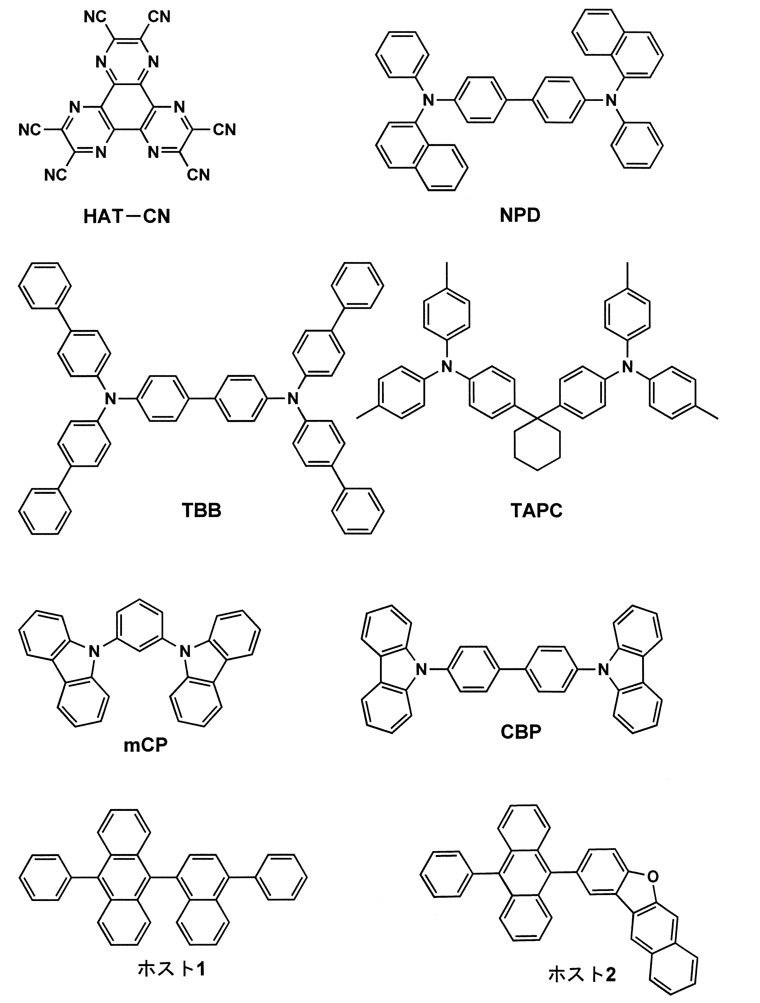
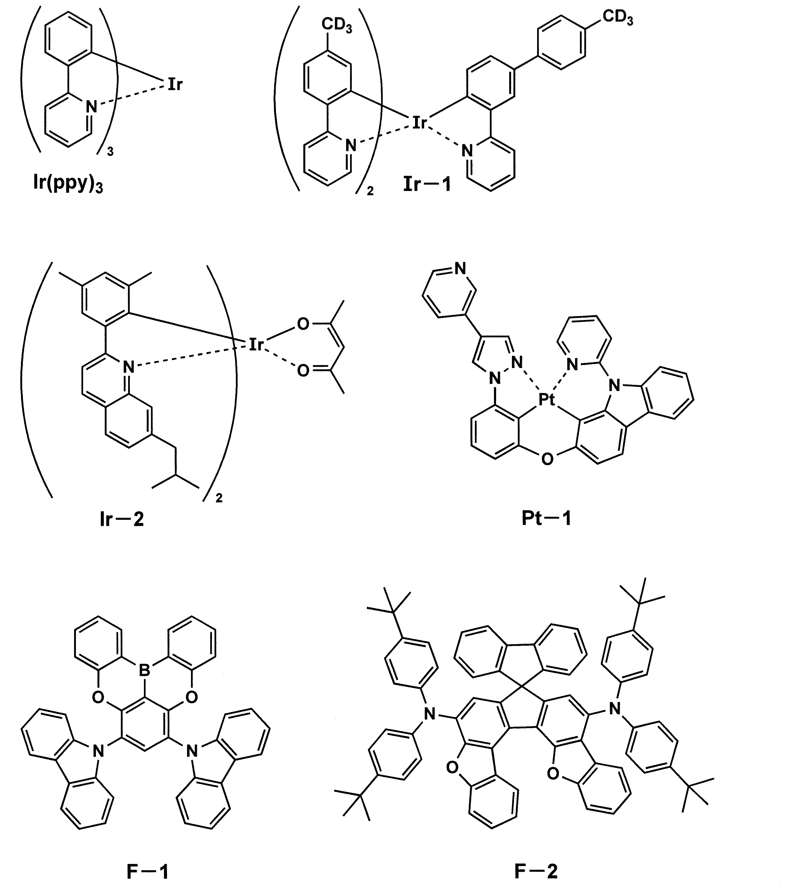


<有機EL素子1-1の作製>
陽極として100mm×100mm×1.1mmのガラス基板上にITO(インジウムチンオキシド)を膜厚100nmで成膜した基板(AvanStrate社製NA45)にパターニングを行った。その後、このITO透明電極を設けた透明支持基板をイソプロピルアルコールで超音波洗浄し、乾燥窒素ガスで乾燥し、UVオゾン洗浄を5分間行った。
陽極として100mm×100mm×1.1mmのガラス基板上にITO(インジウムチンオキシド)を膜厚100nmで成膜した基板(AvanStrate社製NA45)にパターニングを行った。その後、このITO透明電極を設けた透明支持基板をイソプロピルアルコールで超音波洗浄し、乾燥窒素ガスで乾燥し、UVオゾン洗浄を5分間行った。
この透明支持基板上に、ポリ(3,4-エチレンジオキシチオフェン)-ポリスチレンスルホネート(PEDOT/PSS、Bayer社製、Baytron P Al 4083)を純水で70%に希釈した溶液を用いて3000rpm、30秒の条件下、スピンコート法により薄膜を形成した後、200℃にて1時間乾燥し、層厚20nmの正孔注入層を設けた。
その後、ポリビニルカルバゾール(Mw~1100000)を1,2ジクロロベンゼンに溶かした溶液を用いて2000rpm、30秒の条件下、スピンコート法により薄膜を形成した後、120℃にて10分間乾燥し、層厚15nmの正孔輸送層を設けた。
さらに、発光ドーパントとしてIr(ppy)3とホスト化合物として表II記載の比較化合物1が、それぞれ10%、90%の質量%になるようトルエンに溶かした溶液を用い、2000rpm、30秒の条件下、スピンコート法により薄膜を形成した後、100℃にて10分間乾燥し、層厚35nmの発光層を設けた。
次に、この基板を市販の真空蒸着装置の基板ホルダーに固定した。
真空蒸着装置内の蒸着用るつぼの各々に、各層の構成材料を、各々素子作製に最適の量を充填した。蒸着用るつぼはモリブデン製又はタングステン製の抵抗加熱用材料で作製されたものを用いた。
真空度1×10⁻⁴Paまで減圧した後、TPBi(1,3,5-トリス(N-フェニルベンゾイミダゾール-2-イル)を蒸着速度1.0nm/秒で蒸着し、層厚30nmの電子輸送層を形成した。
さらに、フッ化リチウムを膜厚0.5nmで形成した後に、アルミニウム100nmを蒸着して陰極を形成した。
上記素子の非発光面側を、純度99.999%以上の高純度窒素ガスの雰囲気下で、缶状ガラスケースで覆い、電極取り出し配線を設置して、有機EL素子1-1を作製した。
<有機EL素子1-2及び1-3の作製>
ホスト化合物を下記表Iに示すように変えた以外は有機EL素子1-1と同様の方法で有機EL素子1-2及び1-3を作製した。
ホスト化合物を下記表Iに示すように変えた以外は有機EL素子1-1と同様の方法で有機EL素子1-2及び1-3を作製した。
《有機EL素子1-1~1-3の評価》
得られた有機EL素子1-1~1-3を評価するに際しては、上記陰極作製後の各有機EL素子の非発光面を上記の缶状ガラスケースで覆い、厚さ300μmのガラス基板を封止用基板として用いて、周囲にシール材としてエポキシ系光硬化型接着剤(東亞合成社製ラックストラックLC0629B)を適用し、これを陰極上に重ねて透明支持基板と密着させ、ガラス基板側からUV光を照射して硬化させて封止し、図1及び図2に示すような照明装置を作製した。
得られた有機EL素子1-1~1-3を評価するに際しては、上記陰極作製後の各有機EL素子の非発光面を上記の缶状ガラスケースで覆い、厚さ300μmのガラス基板を封止用基板として用いて、周囲にシール材としてエポキシ系光硬化型接着剤(東亞合成社製ラックストラックLC0629B)を適用し、これを陰極上に重ねて透明支持基板と密着させ、ガラス基板側からUV光を照射して硬化させて封止し、図1及び図2に示すような照明装置を作製した。
このようにして作製した各サンプルについて下記の評価を行った。評価結果を表IIに示す。
(2)保存前後の膜密度変化率
分子動力学計算を370Kの条件下で実施して算出した機能性膜の膜密度の値を、該温度下で保存した機能性膜の膜密度の値とし、前記初期膜密度との差を求めた。
分子動力学計算を370Kの条件下で実施して算出した機能性膜の膜密度の値を、該温度下で保存した機能性膜の膜密度の値とし、前記初期膜密度との差を求めた。
○: 各素子の初期膜密度と保存後の膜密度の値の差が初期膜密度に対して1%以下の変化率
×: 各素子の初期膜密度と保存後の膜密度の値の差が初期膜密度に対して1%より大きい変化率
(3)駆動電圧
有機EL素子を室温(約23~25℃)、2.5mA/cm2の定電流条件下で駆動したときの電圧を各々測定し、その測定結果から下記に示すように、有機EL素子1-1を100とする相対値を求めた。
×: 各素子の初期膜密度と保存後の膜密度の値の差が初期膜密度に対して1%より大きい変化率
(3)駆動電圧
有機EL素子を室温(約23~25℃)、2.5mA/cm2の定電流条件下で駆動したときの電圧を各々測定し、その測定結果から下記に示すように、有機EL素子1-1を100とする相対値を求めた。
駆動電圧=(各素子の駆動電圧/有機EL素子1-1の駆動電圧)×100
なお、値が小さい方が比較例に対して駆動電圧が低いことを示す。
なお、値が小さい方が比較例に対して駆動電圧が低いことを示す。
(4)外部取り出し量子効率(「発光効率」ともいう。)
上記有機EL素子を用いて室温(約23~25℃)、2.5mA/cm2の定電流条件下による点灯を行い、点灯開始直後の発光輝度(L)[cd/m2]を測定することにより、外部取り出し量子効率(η)を算出した。
上記有機EL素子を用いて室温(約23~25℃)、2.5mA/cm2の定電流条件下による点灯を行い、点灯開始直後の発光輝度(L)[cd/m2]を測定することにより、外部取り出し量子効率(η)を算出した。
ここで、発光輝度の測定はCS-1000(コニカミノルタセンシング社製)を用いて行い、外部取り出し量子効率は有機EL素子1-1を100とする相対値で表した。
(5)半減寿命
下記に示す測定方法に従って、半減寿命の評価を行った。
下記に示す測定方法に従って、半減寿命の評価を行った。
各有機EL素子を初期輝度1000cd/m2を与える電流で定電流駆動して、初期輝度の1/2(500cd/m2)になる時間を求め、これを半減寿命の尺度とした。なお、半減寿命は有機EL素子1-1を100とする相対値で表した。
(6)駆動時の電圧上昇
有機EL素子を室温(約23~25℃)、2.5mA/cm2の定電流条件下で駆動したときの電圧を各々測定し、その測定結果から下記計算式より駆動時の電圧上昇を求めた。なお、駆動時の電圧上昇は有機EL素子1-1を100とする相対値で表した。
有機EL素子を室温(約23~25℃)、2.5mA/cm2の定電流条件下で駆動したときの電圧を各々測定し、その測定結果から下記計算式より駆動時の電圧上昇を求めた。なお、駆動時の電圧上昇は有機EL素子1-1を100とする相対値で表した。
駆動時の電圧上昇=輝度半減時の駆動電圧-初期駆動電圧
なお、値が小さいほうが比較例に対して駆動時の電圧上昇が小さいことを示す。
なお、値が小さいほうが比較例に対して駆動時の電圧上昇が小さいことを示す。

表IIから明らかなとおり、本発明に係る化合物を用いると、初期膜密度が小さく、保存前後の膜密度変化率が優位に小さいことが分かった。
更に、比較例の有機EL素子に比べ、発光効率及び発光寿命に優れ、低駆動電圧であることが明らかであり、また駆動時の電圧上昇も抑えられることも分かった。
〔実施例3〕
<有機EL素子2-1の作製>
100mm×100mm×1.1mmのガラス基板上に、陽極としてITO(インジウムチンオキシド)を100nmの厚さで成膜した基板(AvanStrate株式会社製、NA-45)にパターニングを行った。その後、このITO透明電極を設けた透明支持基板をイソプロピルアルコールで超音波洗浄し、乾燥窒素ガスで乾燥し、UVオゾン洗浄を5分間行った。
〔実施例3〕
<有機EL素子2-1の作製>
100mm×100mm×1.1mmのガラス基板上に、陽極としてITO(インジウムチンオキシド)を100nmの厚さで成膜した基板(AvanStrate株式会社製、NA-45)にパターニングを行った。その後、このITO透明電極を設けた透明支持基板をイソプロピルアルコールで超音波洗浄し、乾燥窒素ガスで乾燥し、UVオゾン洗浄を5分間行った。
この透明支持基板を市販の真空蒸着装置の基板ホルダーに固定し、一方モリブデン製抵抗加熱ボートに正孔輸送材料としてNPDを200mg入れ、別のモリブデン製抵抗加熱ボートにドーパントとしてF-1を200mg入れ、別のモリブデン製抵抗加熱ボートにホスト化合物1として比較化合物2を200mg入れ、別のモリブデン製抵抗加熱ボートにホスト化合物2としてCBPを200mg入れ、別のモリブデン製抵抗加熱ボートに正孔阻止材料としてBCPを200mg入れ、更に別のモリブデン製抵抗加熱ボートに電子輸送材料としてAlq3を200mg入れ、真空蒸着装置に取り付けた。
次いで、真空槽を4×10⁻⁴Paまで減圧した後、NPDの入った加熱ボートに通電して加熱し、蒸着速度0.1nm/秒で透明支持基板に蒸着し、層厚10nmの正孔輸送層を形成した。
更に、F-1、CBPと比較化合物2の入った加熱ボートに通電して加熱し、それぞれ蒸着速度0.06nm/秒、0.20nm/秒、0.74nm/秒で正孔輸送層上に共蒸着し、層厚40nmの発光層を形成した。
更に、BCPの入った加熱ボートに通電して加熱し、蒸着速度0.1nm/秒で発光層上に蒸着し、層厚10nmの正孔阻止層を形成した。
更に、Alq3の入った加熱ボートに通電して加熱し、蒸着速度0.1nm/秒で正孔阻止層上に蒸着し、層厚30nmの電子輸送層を形成した。
更に、電子注入層上にマグネシウムと銀を10:1の比率(モル比)で100nm共蒸着して陰極を形成し、有機EL素子2-1を作製した。
更に、電子注入層上にマグネシウムと銀を10:1の比率(モル比)で100nm共蒸着して陰極を形成し、有機EL素子2-1を作製した。
<有機EL素子2-2~2-4の作製>
有機EL素子2-1の作製において、比較化合物2を表IIIに記載の化合物に変更した以外は同様にして、有機EL素子2-2~2-4を各々作製した。
有機EL素子2-1の作製において、比較化合物2を表IIIに記載の化合物に変更した以外は同様にして、有機EL素子2-2~2-4を各々作製した。
《有機EL素子2-1~2-4の評価》
得られた有機EL素子を評価するに際しては、実施例1の有機EL素子1-1~1-3と同様に封止し、図1及び図2に示すような照明装置を作製して評価した。
得られた有機EL素子を評価するに際しては、実施例1の有機EL素子1-1~1-3と同様に封止し、図1及び図2に示すような照明装置を作製して評価した。
このようにして作製した各サンプルに対し、実施例1と同様に、初期膜密度、保存前後の密度変化率、外部取り出し量子効率、半減寿命、駆動電圧及び駆動時の電圧上昇について評価を行った。なお、表IIIにおける保存前後の密度変化率、外部取り出し量子効率、半減寿命、駆動電圧及び駆動時の電圧上昇の測定結果は、有機EL素子2-1の測定値を100とする相対値で表した。
さらに、各サンプルについて更に下記の評価を行った。以上の評価結果を表IIIに示す。
(7)蒸着再現性
同一の材料を用い、同一の方法で有機EL素子を10回作製し、各有機EL素子の半減寿命を測定した後、その平均値を算出した。
同一の材料を用い、同一の方法で有機EL素子を10回作製し、各有機EL素子の半減寿命を測定した後、その平均値を算出した。
○:素子の半減寿命の平均値と、各10個の素子の半減寿命の値との差が、すべて10%以内である
△:素子の半減寿命の平均値と、各10個の素子の半減寿命の値との差が、すべて20%以内である
×:素子の半減寿命の平均値と、各10個の素子の半減寿命の値との差が、20%より大きいものが1つ以上ある
(8)蒸着ボートの焦げ付きの有無
各有機EL素子の作製の際に使用した、本発明に係る芳香族化合物が入ったモリブデン製抵抗加熱ボートを、素子化終了後に開け、蒸着ボート内に焦げ付き(「コゲーション」ともいう。)があるか目視で確認した。
△:素子の半減寿命の平均値と、各10個の素子の半減寿命の値との差が、すべて20%以内である
×:素子の半減寿命の平均値と、各10個の素子の半減寿命の値との差が、20%より大きいものが1つ以上ある
(8)蒸着ボートの焦げ付きの有無
各有機EL素子の作製の際に使用した、本発明に係る芳香族化合物が入ったモリブデン製抵抗加熱ボートを、素子化終了後に開け、蒸着ボート内に焦げ付き(「コゲーション」ともいう。)があるか目視で確認した。
○:加熱後のモリブデン製抵抗加熱ボート内に、焦げ付きが認められない
△:加熱後のモリブデン製抵抗加熱ボート内の一部に、焦げ付きが認められる
×: 加熱後のモリブデン製抵抗加熱ボート内の全てに、焦げ付きが認められる
△:加熱後のモリブデン製抵抗加熱ボート内の一部に、焦げ付きが認められる
×: 加熱後のモリブデン製抵抗加熱ボート内の全てに、焦げ付きが認められる

表IIIから明らかなとおり、本発明に係る化合物を蒸着によって素子作製に用いると、加熱時の分解が起こらず、再現性良く素子を作製することができた。また、初期膜密度が小さく、保存前後の膜密度変化率が優位に小さいことが分かった。
更に、比較例の有機EL素子に比べ、発光効率及び発光寿命に優れ、低駆動電圧であることが明らかであり、また駆動時の電圧上昇も抑えられることも分かった。
また、抵抗加熱ボートの焦げ付きも小さいことが分かった。
〔実施例4〕
<有機EL素子3-1の作製>
陽極として100mm×100mm×1.1mmのガラス基板上にITO(インジウムチンオキシド)を100nm成膜した基板(AvanStrate社製NA45)にパターニングを行った。その後、このITO透明電極を設けた透明支持基板をイソプロピルアルコールで超音波洗浄し、乾燥窒素ガスで乾燥し、UVオゾン洗浄を5分間行った。
<有機EL素子3-1の作製>
陽極として100mm×100mm×1.1mmのガラス基板上にITO(インジウムチンオキシド)を100nm成膜した基板(AvanStrate社製NA45)にパターニングを行った。その後、このITO透明電極を設けた透明支持基板をイソプロピルアルコールで超音波洗浄し、乾燥窒素ガスで乾燥し、UVオゾン洗浄を5分間行った。
この透明支持基板上に、ポリ(3,4-エチレンジオキシチオフェン)-ポリスチレンスルホネート(PEDOT/PSS、Bayer社製、Baytron P Al 4083)を純水で70%に希釈した溶液を用いて3000rpm、30秒の条件下、スピンコート法により薄膜を形成した後、200℃にて1時間乾燥し、層厚20nmの正孔注入層を設けた。
この透明支持基板を市販の真空蒸着装置の基板ホルダーに固定し、この装置の粗排気を油回転ポンプにより行った後、装置内の真空度1.0×10⁻⁴Pa以下になるまでクライオポンプを用いて排気した。
次いで、NPDの入った加熱ボートに通電して加熱し、蒸着速度0.1nm/秒で透明支持基板に蒸着し、層厚30nmの正孔輸送層を形成した。
更に、Pt-1、ホスト1の入った加熱ボートに通電して加熱し、それぞれ蒸着速度0.05nm/秒、0.95nm/秒で正孔輸送層上に共蒸着し、層厚40nmの発光層を形成した。
更に、比較化合物2の入った加熱ボートに通電して加熱し、蒸着速度0.1nm/秒で発光層上に蒸着し、層厚10nmの正孔阻止層を形成した。
更に、Alq3の入った加熱ボートに通電して加熱し、蒸着速度0.1nm/秒で正孔阻止層上に蒸着し、層厚30nmの電子輸送層を形成した。
さらに、フッ化リチウムを膜厚0.5nmで形成した後に、アルミニウム100nmを蒸着して陰極を形成した。
上記素子の非発光面側を、純度99.999%以上の高純度窒素ガスの雰囲気下で、缶状ガラスケースで覆い、電極取り出し配線を設置して、有機EL素子3-1を作製した。
<有機EL素子3-2~3-5の作製>
有機EL素子3-1の作製において、比較化合物2を表IVに記載の化合物に変更した以外は同様にして、有機EL素子3-2~3-5を各々作製した。
有機EL素子3-1の作製において、比較化合物2を表IVに記載の化合物に変更した以外は同様にして、有機EL素子3-2~3-5を各々作製した。
《有機EL素子3-2~3-5の評価》
得られた有機EL素子を評価するに際しては、実施例1の有機EL素子1-1~1-3と同様に封止し、図1及び図2に示すような照明装置を作製して評価した。
得られた有機EL素子を評価するに際しては、実施例1の有機EL素子1-1~1-3と同様に封止し、図1及び図2に示すような照明装置を作製して評価した。
このようにして作製した各サンプルに対し、実施例2と同様に、初期膜密度、保存前後の密度変化率、外部取り出し量子効率、半減寿命、駆動電圧及び駆動時の電圧上昇、蒸着再現性、ボートの焦げ付きの有無について評価を行った。なお、表IVにおける保存前後の密度変化率、外部取り出し量子効率、半減寿命、駆動電圧及び駆動時の電圧上昇の測定結果は、有機EL素子3-1の測定値を100とする相対値で表した。

表IVから明らかなとおり、本発明に係る化合物を蒸着での素子作製に用いると、加熱時の分解が起こらず、再現性良く素子を作製することができた。また、初期膜密度が小さく、保存前後の膜密度変化率が優位に小さいことが分かった。
更に、比較例の有機EL素子に比べ、発光効率及び発光寿命に優れ、低駆動電圧であることが明らかであり、また駆動時の電圧上昇も抑えられることも分かった。これは、キラリティを持つことで、分子自体の物理特性は変わらないため、複数の光学異性体を有していても電圧や輝度等の初期性能の取り崩すことなく膜質変化を抑制でき、経時での安定性を高めることができたためである。
また同様に、抵抗加熱ボートの焦げ付きも小さいことが分かった。
〔実施例5〕
<有機EL素子4-1の作製>
陽極として100mm×100mm×1.1mmのガラス基板上にITO(インジウムチンオキシド)を100nm成膜した基板(AvanStrate社製NA45)にパターニングを行った。その後、このITO透明電極を設けた透明支持基板をイソプロピルアルコールで超音波洗浄し、乾燥窒素ガスで乾燥し、UVオゾン洗浄を5分間行った。
<有機EL素子4-1の作製>
陽極として100mm×100mm×1.1mmのガラス基板上にITO(インジウムチンオキシド)を100nm成膜した基板(AvanStrate社製NA45)にパターニングを行った。その後、このITO透明電極を設けた透明支持基板をイソプロピルアルコールで超音波洗浄し、乾燥窒素ガスで乾燥し、UVオゾン洗浄を5分間行った。
この透明支持基板を市販の真空蒸着装置の基板ホルダーに固定し、真空槽を4×10⁻⁴Paまで減圧した後、NPDの入った加熱ボートに通電して加熱し、蒸着速度0.1nm/秒で透明支持基板に蒸着し、層厚35nmの正孔輸送層を形成した。
更に、mCPの入った加熱ボートに通電して加熱し、蒸着速度0.1nm/秒で正孔輸送層上に蒸着し、層厚10nmの電子阻止層を形成した。
更に、例示化合物9(5CzBN)とmCPの入った加熱ボートに通電して加熱し、それぞれ蒸着速度0.08nm/秒、0.92nm/秒で電子阻止層上に共蒸着し、層厚15nmの発光層を形成した。
更に、PPTの入った加熱ボートに通電して加熱し、蒸着速度0.1nm/秒で発光層上に蒸着し、層厚10nmの正孔阻止層を形成した。
更に、比較化合物2の入った加熱ボートに通電して加熱し、蒸着速度0.1nm/秒で正孔阻止層上に蒸着し、層厚40nmの電子輸送層を形成した。
さらに、フッ化リチウムを膜厚0.8nmで形成した後に、アルミニウム100nmを蒸着して陰極を形成した。
上記素子の非発光面側を、純度99.999%以上の高純度窒素ガスの雰囲気下で、缶状ガラスケースで覆い、電極取り出し配線を設置して、有機EL素子4-1を作製した。
<有機EL素子4-2~4-4の作製>
有機EL素子4-1の作製において、比較化合物2を表Vに記載の化合物に変更した以外は同様にして、有機EL素子4-2~4-4を各々作製した。
有機EL素子4-1の作製において、比較化合物2を表Vに記載の化合物に変更した以外は同様にして、有機EL素子4-2~4-4を各々作製した。
《有機EL素子4-2~4-4の評価》
得られた有機EL素子を評価するに際しては、実施例1の有機EL素子1-1~1-3と同様に封止し、図1及び図2に示すような照明装置を作製して評価した。
得られた有機EL素子を評価するに際しては、実施例1の有機EL素子1-1~1-3と同様に封止し、図1及び図2に示すような照明装置を作製して評価した。
このようにして作製した各サンプルに対し、実施例2と同様に、初期膜密度、保存前後の密度変化率、外部取り出し量子効率、半減寿命、駆動電圧及び駆動時の電圧上昇、蒸着再現性、ボートの焦げ付きの有無について評価を行った。なお、表Vにおける保存前後の密度変化率、外部取り出し量子効率、半減寿命、駆動電圧及び駆動時の電圧上昇の測定結果は、有機EL素子4-1の測定値を100とする相対値で表した。
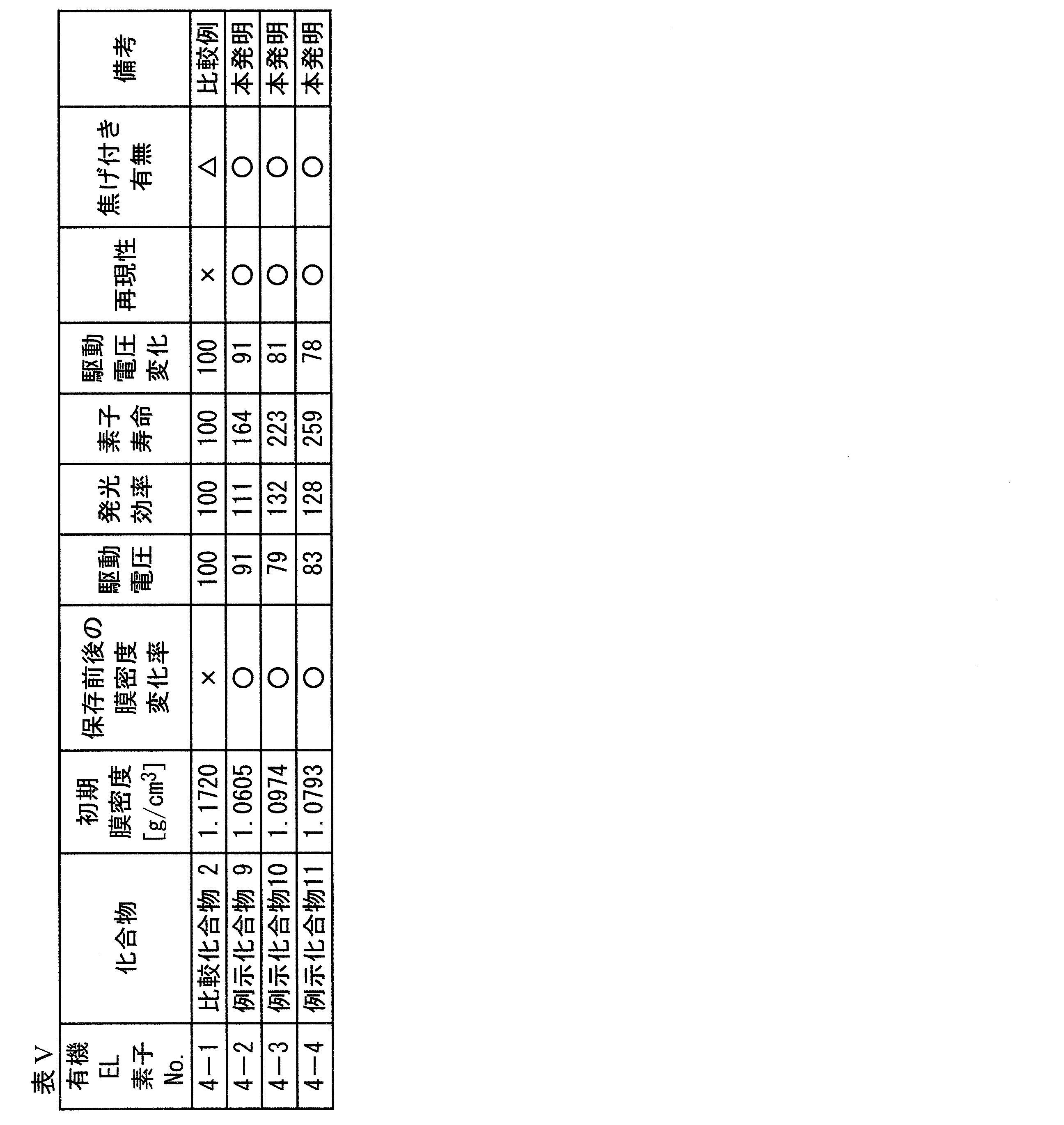
表Vから明らかなとおり、本発明に係る化合物を蒸着による素子作製に用いると、加熱時の分解が起こらず、再現性良く素子を作製することができた。また、初期膜密度が小さく、保存前後の膜密度変化率が優位に小さいことが分かった。
更に、比較例の有機EL素子に比べ、発光効率及び発光寿命に優れ、低駆動電圧であることが明らかであり、また駆動時の電圧上昇も抑えられることも分かった。
また同様に、抵抗加熱ボートの焦げ付きも小さいことが分かった。
〔実施例6〕
<有機EL素子5-1の作製>
陽極として100mm×100mm×1.1mmのガラス基板上にITO(インジウムチンオキシド)を100nm成膜した基板(AvanStrate社製NA45)にパターニングを行った。その後、このITO透明電極を設けた透明支持基板をイソプロピルアルコールで超音波洗浄し、乾燥窒素ガスで乾燥し、UVオゾン洗浄を5分間行った。
<有機EL素子5-1の作製>
陽極として100mm×100mm×1.1mmのガラス基板上にITO(インジウムチンオキシド)を100nm成膜した基板(AvanStrate社製NA45)にパターニングを行った。その後、このITO透明電極を設けた透明支持基板をイソプロピルアルコールで超音波洗浄し、乾燥窒素ガスで乾燥し、UVオゾン洗浄を5分間行った。
この透明支持基板を市販の真空蒸着装置の基板ホルダーに固定し、真空槽を4×10⁻⁴Paまで減圧した後、HAT-CNの入った加熱ボートに通電して加熱し、蒸着速度0.1nm/秒で透明支持基板に蒸着し、層厚10nmの正孔注入層を形成した。
更に、TBBの入った加熱ボートに通電して加熱し、蒸着速度0.1nm/秒で正孔注入層上に蒸着し、層厚30nmの正孔輸送層を形成した。
更に、F-2とIr-1とIr-2とホスト2の入った加熱ボートに通電して加熱し、それぞれ蒸着速度0.08nm/秒、0.92nm/秒で正孔輸送層上に共蒸着し、層厚30nmの発光層を形成した。
更に、比較化合物4の入った加熱ボートに通電して加熱したが、蒸着することはできなかった。
<有機EL素子5-2の作製>
有機EL素子5-1の作製において、発光層の形成までは同様にして作製した。
有機EL素子5-1の作製において、発光層の形成までは同様にして作製した。
更に、比較化合物3の入った加熱ボートに通電して加熱し、蒸着速度0.1nm/秒で発光層上に蒸着し、層厚50nmの電子輸送層を形成した。
さらに、フッ化リチウムを膜厚1nmで形成した後に、アルミニウム100nmを蒸着して陰極を形成した。
上記素子の非発光面側を、純度99.999%以上の高純度窒素ガスの雰囲気下で、缶状ガラスケースで覆い、電極取り出し配線を設置して、有機EL素子5-2を作製した。
<有機EL素子5-3~5-6の作製>
有機EL素子5-2の作製において、比較化合物3を表VIに記載の化合物に変更した以外は同様にして、有機EL素子5-3~5-6を各々作製した。
<有機EL素子5-3~5-6の作製>
有機EL素子5-2の作製において、比較化合物3を表VIに記載の化合物に変更した以外は同様にして、有機EL素子5-3~5-6を各々作製した。
《有機EL素子5-2~5-6の評価》
得られた有機EL素子を評価するに際しては、実施例1の有機EL素子1-1~1-3と同様に封止し、図1及び図2に示すような照明装置を作製して評価した。
得られた有機EL素子を評価するに際しては、実施例1の有機EL素子1-1~1-3と同様に封止し、図1及び図2に示すような照明装置を作製して評価した。
このようにして作製した各サンプルに対し、実施例2と同様に、初期膜密度、保存前後の密度変化率、外部取り出し量子効率、半減寿命、駆動電圧及び駆動時の電圧上昇、蒸着可否(蒸着可能は〇)、蒸着再現性、ボートの焦げ付きの有無について評価を行った。なお、表VIにおける保存前後の密度変化率、外部取り出し量子効率、半減寿命、駆動電圧及び駆動時の電圧上昇の測定結果は、有機EL素子5-2の測定値を100とする相対値で表した。
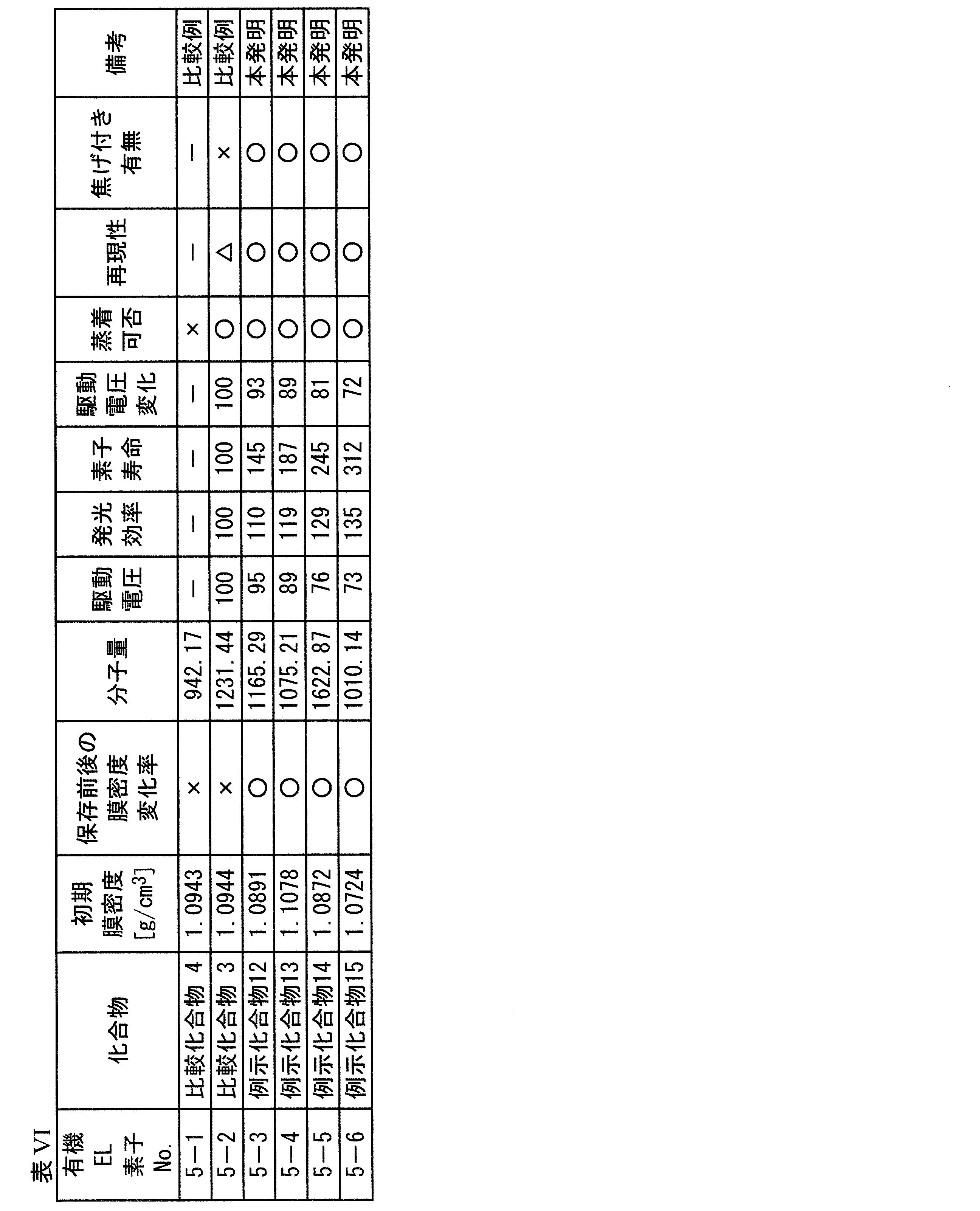
表VIから明らかなとおり、本発明に係る化合物を蒸着での素子作製に用いると、加熱時の分解が起こらず、再現性良く素子を作製することができた。また、初期膜密度が小さく、保存前後の膜密度変化率が優位に小さいことが分かった。
更に、比較例の有機EL素子に比べ、発光効率及び発光寿命に優れ、低駆動電圧であることが明らかであり、また駆動時の電圧上昇も抑えられることも分かった。
また同様に、抵抗加熱ボートの焦げ付きも小さいことが分かった。
〔実施例7〕
<有機EL素子6-1の作製>
陽極として100mm×100mm×1.1mmのガラス基板上にITO(インジウムチンオキシド)を100nm成膜した基板(AvanStrate社製NA45)にパターニングを行った。その後、このITO透明電極を設けた透明支持基板をイソプロピルアルコールで超音波洗浄し、乾燥窒素ガスで乾燥し、UVオゾン洗浄を5分間行った。
<有機EL素子6-1の作製>
陽極として100mm×100mm×1.1mmのガラス基板上にITO(インジウムチンオキシド)を100nm成膜した基板(AvanStrate社製NA45)にパターニングを行った。その後、このITO透明電極を設けた透明支持基板をイソプロピルアルコールで超音波洗浄し、乾燥窒素ガスで乾燥し、UVオゾン洗浄を5分間行った。
この透明支持基板を市販の真空蒸着装置の基板ホルダーに固定し、真空槽を5×10⁻⁴Paまで減圧した後、HAT-CNの入った加熱ボートに通電して加熱し、蒸着速度0.1nm/秒で透明支持基板に蒸着し、層厚10nmの正孔注入層を形成した。
更に、TAPCの入った加熱ボートに通電して加熱し、蒸着速度0.1nm/秒で正孔輸送層上に蒸着し、層厚30nmの正孔輸送層を形成した。
更に、mCPの入った加熱ボートに通電して加熱し、蒸着速度0.1nm/秒で正孔輸送層上に蒸着し、層厚10nmの電子阻止層を形成した。
更に、例示化合物10とPPTの入った加熱ボートに通電して加熱し、それぞれ蒸着速度0.15nm/秒、0.75nm/秒で電子阻止層上に共蒸着し、層厚30nmの発光層を形成した。
更に、PPTの入った加熱ボートに通電して加熱し、蒸着速度0.1nm/秒で発光層上に蒸着し、層厚40nmの電子輸送層を形成した。
さらに、フッ化リチウムを膜厚0.8nmで形成した後に、アルミニウム100nmを蒸着して陰極を形成した。
上記素子の非発光面側を、純度99.999%以上の高純度窒素ガスの雰囲気下で、缶状ガラスケースで覆い、電極取り出し配線を設置して、有機EL素子6-1を作製した。
<有機EL素子6-2~6-6の作製>
有機EL素子6-1の作製において、例示化合物10とPPTの入った加熱ボートに通電して加熱し、それぞれ蒸着速度0.20nm/秒、0.80nm/秒で発光層上に共蒸着し、層厚40nmの電子輸送層を形成した以外は同様にして、有機EL素子6-2を各々作製した。このとき、例示化合物の濃度は20質量%とした。同様に、有機EL素子6-3~6-6の作製において、表VIIに記載の濃度となるように電子輸送層を形成した以外は同様にして、有機EL素子6-3~6-6を各々作製した。
有機EL素子6-1の作製において、例示化合物10とPPTの入った加熱ボートに通電して加熱し、それぞれ蒸着速度0.20nm/秒、0.80nm/秒で発光層上に共蒸着し、層厚40nmの電子輸送層を形成した以外は同様にして、有機EL素子6-2を各々作製した。このとき、例示化合物の濃度は20質量%とした。同様に、有機EL素子6-3~6-6の作製において、表VIIに記載の濃度となるように電子輸送層を形成した以外は同様にして、有機EL素子6-3~6-6を各々作製した。
《有機EL素子6-1~6-6の評価》
得られた有機EL素子を評価するに際しては、実施例1の有機EL素子1-1~1-3と同様に封止し、図1及び図2に示すような照明装置を作製して評価した。
得られた有機EL素子を評価するに際しては、実施例1の有機EL素子1-1~1-3と同様に封止し、図1及び図2に示すような照明装置を作製して評価した。
このようにして作製した各サンプルに対し、実施例2と同様に、外部取り出し量子効率、半減寿命、駆動電圧及び駆動時の電圧上昇、蒸着再現性について評価を行った。なお、表VIIにおける保存前後の密度変化率、外部取り出し量子効率、半減寿命、駆動電圧及び駆動時の電圧上昇の測定結果は、有機EL素子6-1の測定値を100とする相対値で表した。
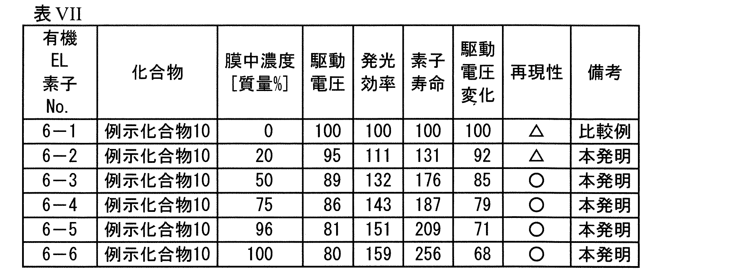
表VIIから明らかなとおり、本発明に係る化合物を蒸着での素子作製に用いると、加熱時の分解が起こらず、再現性良く素子を作製することができた。また、例示化合物10を用いない比較の有機EL素子6-1に比べ、膜中の濃度を上げることで、発光効率及び発光寿命に優れ、低駆動電圧であることが明らかであり、また駆動時の電圧上昇も抑えられることも分かった。
〔実施例8〕
蒸着開始温度として、飽和蒸気圧測定装置VPE-9000(アドバンス理工製)を用い、下記表に示す試料a~dに係る各芳香族化合物について測定を行いった。試料約10mgをパンに乗せ、装置内を真空度1.5×10⁻²Paまで減圧した後、減圧に保ちながら、昇温速度20℃/10分で加熱重量変化を測定した。質量減少曲線の傾きが最大となる温度における曲線の接線と初期質量値の交点を蒸着開始温度とした。
蒸着開始温度として、飽和蒸気圧測定装置VPE-9000(アドバンス理工製)を用い、下記表に示す試料a~dに係る各芳香族化合物について測定を行いった。試料約10mgをパンに乗せ、装置内を真空度1.5×10⁻²Paまで減圧した後、減圧に保ちながら、昇温速度20℃/10分で加熱重量変化を測定した。質量減少曲線の傾きが最大となる温度における曲線の接線と初期質量値の交点を蒸着開始温度とした。
このように測定した蒸着開始温度と各化合物の分子量を下記表VIIIに示した。
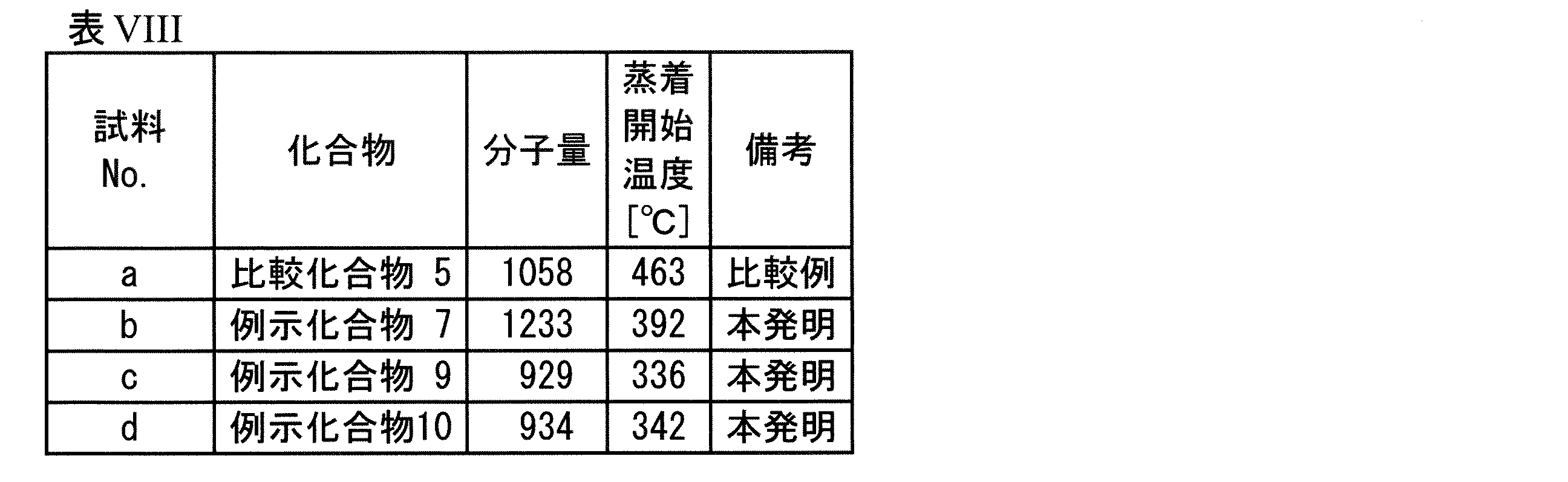
表VIIIから明らかなように、本発明に係る芳香族化合物は分子量が900以上の高分子量であっても蒸着温度の上昇を抑制することができる。特に分子量が1000を超えても、蒸着による素子作製が可能となるため、高Tgで安定性の高い素子を作製することができる。
本発明の機能性膜は、低電圧駆動性、高発光効率、長寿命、駆動電圧変動耐性及び蒸着再現性に優れることによって、有機EL発光装置として、例えば、ディスプレイ用発光装置や照明装置に好適に用いられる。
101 有機EL素子
102 ガラスカバー
105 陰極
106 有機EL層
107 透明電極付きガラス基板
108 窒素ガス
109 捕水剤
102 ガラスカバー
105 陰極
106 有機EL層
107 透明電極付きガラス基板
108 窒素ガス
109 捕水剤
Claims (15)
- 芳香族化合物を含有する機能性膜であって、
前記芳香族化合物が、縮合若しくは非縮合型の6員の、芳香族炭化水素環又は芳香族複素環に14π電子以上のπ電子を含む縮合芳香族環基を4個以上有し、前記14π電子以上のπ電子を含む縮合芳香族環基を置換基として3つ以上隣接して有する芳香族化合物であり、
前記芳香族化合物について、300KにおいてNPTアンサンブルの分子動力学計算で算出した膜密度の値を、前記芳香族化合物のみを含有する機能性膜の初期膜密度とし、
前記芳香族化合物について、370Kにおいて前記分子動力学計算で算出した膜密度の値を、当該温度下で保存した機能性膜の保存後の膜密度の値としたときに、前記初期膜密度と前記保存後の膜密度の値の差が、前記初期膜密度に対して1%以下であることを特徴とする機能性膜。 - 前記初期膜密度の値が、1.00~1.20g/cm3の範囲内であることを特徴とする請求項1に記載の機能性膜。
- 前記芳香族化合物が、キラリティ発生部位を有することを特徴とする請求項1又は請求項2に記載の機能性膜。
- 前記芳香族化合物が、下記一般式(1)で表される構造を有することを特徴とする請求項1から請求項3までのいずれか一項に記載の機能性膜。

- 前記芳香族化合物が、一般式(2)で表される構造を有することを特徴とする請求項1から請求項4までのいずれか一項に記載の機能性膜。

- 前記14π電子以上のπ電子を含む縮合芳香族複素環基が、窒素(N)原子を有することを特徴とする請求項1から請求項5までのいずれか一項に記載の機能性膜。
- 前記14π電子以上のπ電子を含む縮合芳香族複素環基が、少なくとも2つは窒素(N)原子を有することを特徴とする請求項1から請求項6までのいずれか一項に記載の機能性膜。
- 前記芳香族化合物が有する14π電子以上のπ電子を含む縮合芳香族環基が、5個以下であることを特徴とする請求項1から請求項7までのいずれか一項に記載の機能性膜。
- 前記一般式(2)で表される構造を有する化合物において、R2が、R1を表すか、シクロアルキル基、芳香族炭化水素基、芳香族複素環基、アミノ基、フッ化炭化水素基、ニトロ基、シリル基及びホスホノ基から選ばれるいずれかの基を表すことを特徴とする請求項5に記載の機能性膜。
- 前記芳香族化合物の分子量が、1000~2000の範囲内であることを特徴とする請求項1から請求項9までのいずれか一項に記載の機能性膜。
- 前記芳香族化合物を、50質量%以上含有することを特徴とする請求項1から請求項10までのいずれか一項に記載の機能性膜。
- 請求項1から請求項11までのいずれか一項に記載の機能性膜が、電荷輸送性膜であることを特徴とする機能性膜。
- 請求項1から請求項12までのいずれか一項に記載の機能性膜を、真空蒸着法により形成することを特徴とする機能性膜の形成方法。
- 少なくとも、一対の電極と一つ又は複数の層とを有する有機エレクトロルミネッセンス素子であって、前記複数の層の少なくとも一層が、請求項1から請求項12までのいずれか一項に記載の機能性膜を有することを特徴とする有機エレクトロルミネッセンス素子。
- 前記複数の層のうち、隣接した少なくとも2層が請求項1から請求項12までのいずれか一項に記載の機能性膜であることを特徴とする請求項14に記載の有機エレクトロルミネッセンス素子。
Priority Applications (2)
| Application Number | Priority Date | Filing Date | Title |
|---|---|---|---|
| JP2021507201A JP7405135B2 (ja) | 2019-03-19 | 2020-03-06 | 機能性膜、その形成方法及び有機エレクトロルミネッセンス素子 |
| US17/440,353 US20220190257A1 (en) | 2019-03-19 | 2020-03-06 | Functional film, method for forming same, and organic electroluminescent element |
Applications Claiming Priority (2)
| Application Number | Priority Date | Filing Date | Title |
|---|---|---|---|
| JP2019-050713 | 2019-03-19 | ||
| JP2019050713 | 2019-03-19 |
Publications (1)
| Publication Number | Publication Date |
|---|---|
| WO2020189330A1 true WO2020189330A1 (ja) | 2020-09-24 |
Family
ID=72521017
Family Applications (1)
| Application Number | Title | Priority Date | Filing Date |
|---|---|---|---|
| PCT/JP2020/009624 Ceased WO2020189330A1 (ja) | 2019-03-19 | 2020-03-06 | 機能性膜、その形成方法及び有機エレクトロルミネッセンス素子 |
Country Status (3)
| Country | Link |
|---|---|
| US (1) | US20220190257A1 (ja) |
| JP (1) | JP7405135B2 (ja) |
| WO (1) | WO2020189330A1 (ja) |
Cited By (3)
| Publication number | Priority date | Publication date | Assignee | Title |
|---|---|---|---|---|
| JPWO2020189283A1 (ja) * | 2019-03-18 | 2020-09-24 | ||
| CN114656467A (zh) * | 2020-12-22 | 2022-06-24 | 广州华睿光电材料有限公司 | 有机化合物、混合物、组合物及有机电子器件 |
| CN114671857A (zh) * | 2022-03-07 | 2022-06-28 | 宁波卢米蓝新材料有限公司 | 一种有机化合物及其在有机电致发光器件中的应用 |
Citations (4)
| Publication number | Priority date | Publication date | Assignee | Title |
|---|---|---|---|---|
| WO2015022835A1 (ja) * | 2013-08-14 | 2015-02-19 | コニカミノルタ株式会社 | 有機エレクトロルミネッセンス素子、照明装置、表示装置及び蛍光発光性化合物 |
| CN108264478A (zh) * | 2016-12-30 | 2018-07-10 | 昆山国显光电有限公司 | 载流子传输材料及载流子传输层及有机发光器件 |
| JP2018519663A (ja) * | 2015-06-16 | 2018-07-19 | 昆山国顕光電有限公司Kunshan Go−Visionox Opto−Electronics Co., Ltd. | 有機エレクトロルミネッセンス装置及びその製造方法 |
| WO2018155642A1 (ja) * | 2017-02-24 | 2018-08-30 | 国立大学法人九州大学 | 化合物、発光材料および発光素子 |
Family Cites Families (7)
| Publication number | Priority date | Publication date | Assignee | Title |
|---|---|---|---|---|
| JP4810805B2 (ja) * | 2003-07-31 | 2011-11-09 | 三菱化学株式会社 | 有機化合物、電荷輸送材料、有機電界発光素子材料および有機電界発光素子 |
| EP4498784A3 (en) * | 2018-03-30 | 2025-04-23 | Kyulux, Inc. | Composition of matter for use in organic light-emitting diodes |
| WO2020059520A1 (ja) * | 2018-09-21 | 2020-03-26 | コニカミノルタ株式会社 | ベンゾニトリル誘導体及びその製造方法、インク組成物、有機エレクトロルミネッセンス素子材料、発光材料、電荷輸送材料、発光性薄膜及び有機エレクトロルミネッセンス素子 |
| JPWO2020059326A1 (ja) * | 2018-09-21 | 2021-09-16 | コニカミノルタ株式会社 | ベンゾニトリル誘導体及びその製造方法、インク組成物、有機エレクトロルミネッセンス素子材料、発光材料、電荷輸送材料、発光性薄膜及び有機エレクトロルミネッセンス素子 |
| KR102647025B1 (ko) * | 2018-12-28 | 2024-03-12 | 엘지디스플레이 주식회사 | 발광 특성이 우수한 유기 화합물, 이를 포함하는 유기발광다이오드 및 유기발광장치 |
| JPWO2020189283A1 (ja) * | 2019-03-18 | 2020-09-24 | ||
| WO2020189236A1 (ja) * | 2019-03-18 | 2020-09-24 | コニカミノルタ株式会社 | 有機膜及び有機エレクトロルミネッセンス素子 |
-
2020
- 2020-03-06 WO PCT/JP2020/009624 patent/WO2020189330A1/ja not_active Ceased
- 2020-03-06 US US17/440,353 patent/US20220190257A1/en active Pending
- 2020-03-06 JP JP2021507201A patent/JP7405135B2/ja active Active
Patent Citations (4)
| Publication number | Priority date | Publication date | Assignee | Title |
|---|---|---|---|---|
| WO2015022835A1 (ja) * | 2013-08-14 | 2015-02-19 | コニカミノルタ株式会社 | 有機エレクトロルミネッセンス素子、照明装置、表示装置及び蛍光発光性化合物 |
| JP2018519663A (ja) * | 2015-06-16 | 2018-07-19 | 昆山国顕光電有限公司Kunshan Go−Visionox Opto−Electronics Co., Ltd. | 有機エレクトロルミネッセンス装置及びその製造方法 |
| CN108264478A (zh) * | 2016-12-30 | 2018-07-10 | 昆山国显光电有限公司 | 载流子传输材料及载流子传输层及有机发光器件 |
| WO2018155642A1 (ja) * | 2017-02-24 | 2018-08-30 | 国立大学法人九州大学 | 化合物、発光材料および発光素子 |
Cited By (5)
| Publication number | Priority date | Publication date | Assignee | Title |
|---|---|---|---|---|
| JPWO2020189283A1 (ja) * | 2019-03-18 | 2020-09-24 | ||
| CN114656467A (zh) * | 2020-12-22 | 2022-06-24 | 广州华睿光电材料有限公司 | 有机化合物、混合物、组合物及有机电子器件 |
| CN114656467B (zh) * | 2020-12-22 | 2024-06-25 | 广州华睿光电材料有限公司 | 有机化合物、混合物、组合物及有机电子器件 |
| CN114671857A (zh) * | 2022-03-07 | 2022-06-28 | 宁波卢米蓝新材料有限公司 | 一种有机化合物及其在有机电致发光器件中的应用 |
| CN114671857B (zh) * | 2022-03-07 | 2024-02-09 | 宁波卢米蓝新材料有限公司 | 一种有机化合物及其在有机电致发光器件中的应用 |
Also Published As
| Publication number | Publication date |
|---|---|
| US20220190257A1 (en) | 2022-06-16 |
| JP7405135B2 (ja) | 2023-12-26 |
| JPWO2020189330A1 (ja) | 2020-09-24 |
Similar Documents
| Publication | Publication Date | Title |
|---|---|---|
| KR102241439B1 (ko) | 유기 일렉트로루미네센스 소자, 유기 일렉트로루미네센스 소자의 제조 방법, 표시 장치 및 조명 장치 | |
| US10109800B2 (en) | Organic electroluminescent element, display device and lighting device | |
| JP5011908B2 (ja) | 有機エレクトロルミネッセンス素子、表示装置および照明装置 | |
| JP5593696B2 (ja) | 有機エレクトロルミネッセンス素子の製造方法 | |
| JP5088025B2 (ja) | 有機エレクトロルミネッセンス材料、有機エレクトロルミネッセンス素子、表示装置及び照明装置 | |
| JP2014068027A (ja) | 有機エレクトロルミネッセンス素子、表示装置及び照明装置 | |
| US20150333272A1 (en) | Transparent electrode, electronic device, and organic electroluminescent element | |
| JP6225915B2 (ja) | 有機エレクトロルミネッセンス素子 | |
| JPWO2008035595A1 (ja) | 有機エレクトロルミネッセンス素子 | |
| US20140377546A1 (en) | Transparent electrode, electronic device, and organic electroluminescent element | |
| JP2009013366A (ja) | 有機エレクトロルミネッセンス素子材料、有機エレクトロルミネッセンス素子、表示装置及び照明装置 | |
| JP2014044972A (ja) | 有機エレクトロルミネッセンス素子、表示装置、照明装置及び有機エレクトロルミネッセンス素子の製造方法 | |
| JP2012153753A (ja) | 有機エレクトロルミネッセンス素子材料、有機エレクトロルミネッセンス素子と、表示装置及び照明装置 | |
| JP6939795B2 (ja) | 透明電極及び電子デバイス | |
| JP5560517B2 (ja) | 有機エレクトロルミネッセンス素子、表示装置及び照明装置 | |
| JP7405135B2 (ja) | 機能性膜、その形成方法及び有機エレクトロルミネッセンス素子 | |
| JP2012023127A (ja) | 有機エレクトロルミネッセンス素子、その製造方法、及び照明装置 | |
| JP2012099515A (ja) | 有機エレクトロルミネッセンス素子材料、有機エレクトロルミネッセンス素子とその製造方法、表示装置及び照明装置 | |
| JPWO2009008263A1 (ja) | 有機エレクトロルミネッセンス材料、有機エレクトロルミネッセンス素子、表示装置及び照明装置 | |
| US20150118507A1 (en) | Transparent electrode, electronic device, and organic electroluminescence element | |
| JP5521753B2 (ja) | 有機エレクトロルミネッセンス素子 | |
| JP6295958B2 (ja) | 透明電極、電子デバイス及び有機エレクトロルミネッセンス素子 | |
| WO2018221173A1 (ja) | 有機エレクトロルミネッセンス素子、表示装置及び照明装置 | |
| JP6028668B2 (ja) | 透明電極、電子デバイス及び有機エレクトロルミネッセンス素子 | |
| JP6187471B2 (ja) | 透明電極、電子デバイス及び有機エレクトロルミネッセンス素子 |
Legal Events
| Date | Code | Title | Description |
|---|---|---|---|
| 121 | Ep: the epo has been informed by wipo that ep was designated in this application |
Ref document number: 20773496 Country of ref document: EP Kind code of ref document: A1 |
|
| ENP | Entry into the national phase |
Ref document number: 2021507201 Country of ref document: JP Kind code of ref document: A |
|
| NENP | Non-entry into the national phase |
Ref country code: DE |
|
| 122 | Ep: pct application non-entry in european phase |
Ref document number: 20773496 Country of ref document: EP Kind code of ref document: A1 |