WO2020189322A1 - 有機半導体素子の製造方法 - Google Patents
有機半導体素子の製造方法 Download PDFInfo
- Publication number
- WO2020189322A1 WO2020189322A1 PCT/JP2020/009571 JP2020009571W WO2020189322A1 WO 2020189322 A1 WO2020189322 A1 WO 2020189322A1 JP 2020009571 W JP2020009571 W JP 2020009571W WO 2020189322 A1 WO2020189322 A1 WO 2020189322A1
- Authority
- WO
- WIPO (PCT)
- Prior art keywords
- electrode
- organic semiconductor
- manufacturing
- base material
- self
- Prior art date
- Legal status (The legal status is an assumption and is not a legal conclusion. Google has not performed a legal analysis and makes no representation as to the accuracy of the status listed.)
- Ceased
Links
Images











Classifications
-
- H—ELECTRICITY
- H10—SEMICONDUCTOR DEVICES; ELECTRIC SOLID-STATE DEVICES NOT OTHERWISE PROVIDED FOR
- H10K—ORGANIC ELECTRIC SOLID-STATE DEVICES
- H10K10/00—Organic devices specially adapted for rectifying, amplifying, oscillating or switching; Organic capacitors or resistors having potential barriers
- H10K10/40—Organic transistors
-
- H—ELECTRICITY
- H10—SEMICONDUCTOR DEVICES; ELECTRIC SOLID-STATE DEVICES NOT OTHERWISE PROVIDED FOR
- H10D—INORGANIC ELECTRIC SEMICONDUCTOR DEVICES
- H10D30/00—Field-effect transistors [FET]
- H10D30/60—Insulated-gate field-effect transistors [IGFET]
- H10D30/67—Thin-film transistors [TFT]
Definitions
- the present invention relates to a technique for manufacturing an organic semiconductor element, for example, an organic thin film transistor on a base material such as a glass plate, a resin plate, or a resin sheet.
- Patent Document 1 describes a technique for manufacturing an electrode for a thin film transistor by applying a conductive ink containing metal nanoparticles as a main component to a base material.
- an electrode is formed by applying or printing a conductive ink on the surface of a base material and then firing the electrode, and the electrode is washed with an acidic solution and then a semiconductor layer is laminated.
- the thin film transistor manufactured by the method including such a step is a so-called top gate / bottom contact type.
- Patent Document 1 describes that, in order to modify the electrode surface, a step of modifying the electrode surface with a self-assembled film after cleaning may be provided.
- the present invention has been made in view of the above problems, and proposes a method for manufacturing an organic semiconductor device, which does not perform acid cleaning and can sufficiently secure the conductivity between the electrode and the semiconductor layer. It is the purpose.
- One aspect of the method for manufacturing an organic semiconductor element according to the present invention is a step of forming an electrode on the surface of a base material using an ink containing an electrode material, and on the surface of the base material in order to achieve the above object.
- the electrode which has not been washed with an acidic solution since it was formed, is brought into contact with a treatment liquid containing a self-assembling material to form a self-assembled monolayer with the self-assembling material on the surface of the electrode.
- the step includes a step of laminating an organic semiconductor layer conductive to the electrode via the self-assembled monolayer on the electrode on which the self-assembled monolayer is formed.
- the inventor of the present application has formed a self-assembled monolayer without performing cleaning with an acid after forming the electrodes as described above. It was found that it is effective to bring the electrode into direct contact with the treatment solution of. As will be described later, the organic semiconductor device manufactured by such a manufacturing method is not affected by the organic residue derived from the ink, and is electrically equivalent to the organic semiconductor device manufactured by the manufacturing process involving acid cleaning. It has been confirmed to have performance.
- the treatment liquid containing the self-assembling material is brought into direct contact with the electrodes formed on the substrate by the ink.
- a self-assembled monolayer is formed on the electrode surface, and an organic semiconductor layer is further laminated.
- an organic semiconductor device capable of sufficiently ensuring the conductivity between the electrode and the semiconductor layer without performing acid cleaning.
- FIG. 1 is a flowchart showing an embodiment of a method for manufacturing an organic semiconductor device according to the present invention.
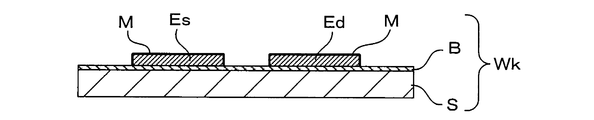
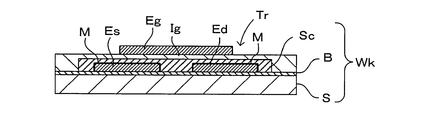
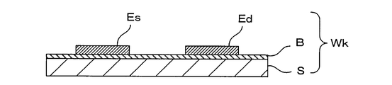
- FIGS. 2A to 2F are diagrams showing structures in each process of the semiconductor element manufactured by this manufacturing method.
- This manufacturing method can be used to form a semiconductor element on various flat plates such as a semiconductor substrate, a glass substrate, and a resin substrate.
- a process for forming an organic thin film transistor as an example of a semiconductor element on the surface of, for example, a glass plate or a polyimide sheet as the substrate S will be described in detail.
- the following methods and devices can be used for forming various semiconductor elements.
- a structure in which various functional layers are laminated on the substrate S is referred to as a "work" which is a processing target in each process, and is designated by a reference numeral Wk.
- the structure of such a structure changes sequentially with the progress of the manufacturing process, and all of them are referred to as work Wk. Further, in the following cross-sectional view of the work, the relative thickness of each layer does not always match the actual one in order to clarify the structural features.
- the substrate to be treated is cleaned with an appropriate cleaning agent (step S101), and the surface of the substrate is cleaned.
- a resin layer to be the base layer B is formed on one surface Sa of the substrate S (step S102).
- the base layer B can be formed, for example, by uniformly applying a solution containing a material of a resin (for example, various polymer resins) that exhibits electrical insulation in a cured state to the substrate surface Sa by, for example, a spin coating method. it can.
- the base layer B can be formed by any forming method capable of forming a uniform layer without being limited to this.
- a firing treatment is performed after the application in order to dry and cure the formed coating film (step S103).
- the coating film is cured to form the base layer B in close contact with the substrate surface Sa.
- a new layer can be formed on the surface of the cured base layer B.
- the base layer B has a function of covering the surface of the substrate S with a uniform and stable insulating layer and maintaining the shape of each layer formed in a subsequent step in a stable manner.
- the base layer B functions as a primer layer to improve the adhesion of the electrodes to the substrate S.
- the polymer resin material constituting the base layer B for example, polyurethane, polyimide, polyamideimide, polyvinyl alcohol, polyvinylphenol, polyester, polyethylene and the like can be used.
- the firing process for curing the polymer can be performed under the conditions of, for example, 120 ° C. for about 30 minutes.
- the firing process can be executed by holding the work Wk for a predetermined time in a heating furnace such as an oven whose temperature is adjusted to a predetermined firing temperature.
- a resin material having low heat resistance can also be used as a substrate.
- the work Wk may be allowed to stand in the heating furnace, or may be heated while being conveyed in the heating furnace.
- the source electrodes Es and drain electrodes Ed constituting the organic semiconductor thin film transistor are formed on the surface of the base layer B using the work Wk in which the base layer B is laminated on the substrate S as a base material.
- Step S104 Various methods can be adopted for forming these electrodes.
- a method applying a printing technique in which an electrode is formed by transferring a preformed electrode pattern to the base layer B will be described.
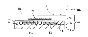
- FIGS. 3A to 3D are diagrams schematically illustrating a method of manufacturing an electrode by printing.
- the electrode pattern PT formed of a conductive material such as metal particles (for example, silver) and a conductive ink containing a solvent is a blanket BL which is a transfer medium formed of a glass plate, a resin plate, or the like.
- a blanket BL which is a transfer medium formed of a glass plate, a resin plate, or the like.
- two electrode pattern PTs separated from each other are supported on the pattern supporting surface (lower surface in the figure) of the blanket BL.
- These two electrode patterns PT finally function as source electrodes and drain electrodes, respectively.
- the blanket BL is arranged close to the work Wk with the pattern supporting surface facing the surface of the base layer B. From this state, as shown in FIG. 3B, the roller member RL is brought into contact with the blanket BL surface on the side opposite to the pattern supporting surface. The roller member RL rolls along the surface of the blanket BL while pushing the blanket BL toward the work Wk side. By doing so, the electrode pattern PT supported on the blanket BL is pressed against the base layer B and finally transferred to the surface of the base layer B. The blanket BL after transfer is carried out from the vicinity of the work Wk.
- Such an electrode forming process is subdivided into a patterning step of forming an electrode pattern PT with conductive ink on the blanket BL and a transfer step of transferring the formed electrode pattern PT to the work Wk. can do.
- the patterning step and the transfer step can be performed using the same processing apparatus. The process described here can be performed, for example, by the transfer apparatus described in JP-A-2014-144628, which was previously disclosed by the applicant of the present application.
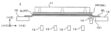
- FIGS. 4A to 4D are diagrams showing the process of electrode forming processing. Further, FIG. 5A is a schematic diagram showing a patterning process, and FIG. 5B is a schematic diagram showing a transfer process.
- the XY plane represents the horizontal plane. Further, the Z direction represents the vertical direction, and more specifically, the (+ Z) direction represents the vertical upward direction.
- the patterning process will be described with reference to FIGS. 4A to 4D.
- the upper stage 11 having a vacuum suction surface on the lower surface and the lower stage 12 having a frame shape with a large opening at the center are arranged close to each other in a horizontal posture. There is.
- the opening size of the opening 121 of the lower stage 12 is larger than the plane size of the upper stage 11.
- a plurality of elevating hands 13 are arranged so as to be individually supported by an elevating mechanism (not shown).
- a cylindrical or cylindrical pressing roller 14 extending in the Y direction is arranged near the ( ⁇ X) side end of the opening 121.
- the pressing roller 14 is rotatably supported around the central axis in the Y direction by the support member 15.
- the support member 15 can move up and down in the Z direction and travel in the X direction by a drive mechanism (not shown).
- the pressing roller 14 has a function corresponding to the roller member RL shown in FIG. 3B.
- a plate PP having a convex pattern obtained by reversing a desired electrode pattern is carried into the transfer device 1 and set on the upper stage 11.
- the upper stage 11 attracts and holds the plate PP with the pattern forming surface on which the convex pattern is formed facing downward.
- the blanket BL to which the conductive ink Ik is uniformly applied is carried into the transfer device 1 and set on the lower stage 12.
- the lower stage 12 attracts and holds the peripheral edge portion of the blanket BL in a state where the surface coated with the conductive ink Ik faces upward and faces the plate PP.
- each elevating hand 13 is positioned at a height such that the upper surface thereof is the same height as the upper surface of the lower stage 12.
- the central portion of the blanket BL in the open state is maintained in the horizontal posture.
- the pressing roller 14 is positioned below the ( ⁇ X) side end of the plate PP in the horizontal direction and at a position where the upper end is separated from the lower surface of the blanket BL in the vertical direction.
- the support member 15 raises the pressing roller 14, so that the pressing roller 14 comes into contact with the lower surface of the blanket BL.
- the pressing roller 14 continues to rise even after coming into contact with the lower surface of the blanket BL.
- the blanket BL is pushed up by the pressing roller 14, and finally the upper surface of the blanket BL comes into contact with the lower surface of the plate PP.
- the ink Ik supported on the upper surface of the blanket BL comes into close contact with the plate PP.
- the pressing roller 14 pushes up the blanket BL, so that the ink Ik is pressed against the plate PP with a predetermined pressing force.
- the support member 15 moves the pressing roller 14 in the (+ X) direction.
- the pressing roller 14 comes into contact with the lower surface of the blanket BL and travels in the (+ X) direction while being driven to rotate.
- the region where the blanket BL and the plate PP are in close contact with each other via the ink Ik expands in the X direction.
- each of the plurality of elevating hands 13 sequentially descends with the movement of the support member 15 in order to avoid interference with the traveling pressing roller 14.
- FIG. 4D when the pressing roller 14 reaches the end position just below the (+ X) side end of the plate PP, the entire plate PP is in contact with the blanket BL.
- the portion of the ink Ik uniformly applied to the blanket BL that corresponds to the convex pattern shifts to the plate PP, and the other portion remains on the blanket BL. ..
- the ink Ik is patterned by the convex pattern, and the inverted pattern of the convex pattern is transferred to the blanket BL as the electrode pattern PT.
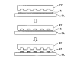
- FIG. 5A is a diagram schematically showing a process in which the ink Ik applied to the blanket BL is patterned by the plate PP to form the electrode pattern PT.
- the transfer step of transferring the electrode pattern PT formed on the blanket BL to the work Wk can be explained by replacing the plate PP in the above process with the work Wk and the ink Ik with the electrode pattern PT. That is, the blanket BL on which the electrode pattern PT is supported is held by the lower stage 12, and the work Wk to which the pattern is transferred is held by the upper stage 11 (FIG. 4A).
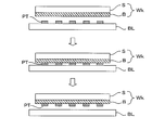
- FIG. 5B is a diagram schematically showing a process (step S104 of FIG. 1) in which the electrode pattern PT is transferred to the work Wk in which the base layer B is formed on the substrate S.
- the above electrode forming treatment applies a parallel plate printing technique in which the electrode pattern PT is transferred from the blanket BL to the work Wk by bringing the blanket BL having a flat plate shape and the work Wk into close contact with each other and then peeling them off. It is a thing.
- the method for forming the electrode pattern PT on the work Wk is not limited to this, and various methods can be applied, for example, as illustrated below.
- FIG. 6 is a diagram showing another aspect of the electrode forming process.
- a transfer device 2 is used for this process.
- the blanket 22 is wound around the surface of the cylindrical blanket body 21.
- the electrode pattern PT is patterned on the intaglio 23. While rotating the blanket body 21 at a predetermined speed, the intaglio 23 moves while abutting against the blanket 22. As a result, the electrode pattern PT patterned by the intaglio 23 is transferred to the blanket 22.
- the stage 24 moves while bringing the work Wk placed on the stage 24 into contact with the blanket BL. As a result, the electrode pattern PT on the blanket BL is transferred to the work Wk.
- This method corresponds to the offset intaglio printing technique. It is also possible to form an electrode on the work Wk by such a method.
- pattern formation on a flat plate or a cylindrical blanket may be performed by another method.
- the electrode pattern may be formed by partially landing the conductive ink on the blanket surface using a printing technique such as a screen printing method or an inkjet method.
- a printing technique such as a screen printing method or an inkjet method.
- a firing process is performed on the work Wk after the pattern transfer (step S105).
- the firing conditions at this time can be, for example, 120 ° C. for 30 minutes. However, it is not essential that the conditions are the same as those of the firing process in step S103.
- the work Wk at this point is in a state in which the source electrode Es and the drain electrode Ed are formed on the upper surface of the base layer B by curing the electrode pattern. It has become.
- a SAM treatment for modifying the surface of the formed electrode is executed (step S106).
- the SAM treatment is a treatment for forming a self-assembled monolayer (SAM) on the surface of the electrode in order to improve the conductivity between the electrode and the semiconductor layer laminated on the electrode. .. Since the principle and method of SAM treatment are known, an example of a method of forming a SAM film by wet treatment will be briefly described here.
- a solution in which isopropyl alcohol (IPA) as a solvent is dissolved in pentafluorobenzenethiol (PFBT) having a concentration of about 0.01 M as a self-assembling material (hereinafter, may be referred to as "SAM treatment solution").
- SAM treatment solution A solution in which isopropyl alcohol (IPA) as a solvent is dissolved in pentafluorobenzenethiol (PFBT) having a concentration of about 0.01 M as a self-assembling material (hereinafter, may be referred to as "SAM treatment solution”).
- SAM treatment solution A solution in which isopropyl alcohol (IPA) as a solvent is dissolved in pentafluorobenzenethiol (PFBT) having a concentration of about 0.01 M as a self-assembling material.
- the organic semiconductor layer is laminated so as to cover the surface of the work Wk on which the electrodes Es and Ed are formed (step S107).
- the organic semiconductor layer can be formed by using, for example, a known vacuum vapor deposition method. As shown in FIG. 2D, the work Wk at this point is in a state in which the monolayer M covering the electrodes Es and Ed and the surface of the exposed base layer B are continuously covered by the organic semiconductor layer Sc. ing.
- a gate insulating layer covering the surface of the organic semiconductor film Sc is formed (step S108).
- the gate insulating layer is formed by depositing, for example, an electrically insulating material (for example, parylene) on the surface of the organic semiconductor film Sc using a known chemical vapor deposition (CVD). Thereby, it can be formed.
- CVD chemical vapor deposition
- the work Wk at this point is in a state where the entire surface of the organic semiconductor layer Sc is covered with the continuous gate insulating layer Ig.
- a gate electrode is formed on the surface of the gate insulating layer Ig (step S109).
- the gate electrode by the same technique as the formation of the source electrode Es and the drain electrode Ed. That is, as shown in FIG. 3D, the blanket BL supporting the electrode pattern PT serving as the gate electrode is arranged close to the work Wk, and the blanket BL is pressed by the roller member RL to transfer the electrode pattern PT to the gate insulating layer Ig. Transfer to the surface.
- the gate electrode Eg is formed on the surface of the gate insulating layer Ig.
- the electrode can also be formed by forming a metal thin film by vacuum vapor deposition.
- the electrode material for example, a metal material such as gold or silver can be used.
- the substrate S, the base layer B, the source and drain electrodes Es and Ed, the organic semiconductor layer Sc, the monolayer M, the gate insulating layer Ig, and the gate electrode Eg are laminated in this order.
- the source and drain electrodes Es and Ed, the organic semiconductor layer Sc, the gate insulating layer Ig, and the gate electrode Eg collectively function as an organic thin film transistor Tr.
- the substrate S and the base layer B function as a base material that supports the organic thin film transistor Tr. In the actual manufacturing process, a large number of organic thin film transistors Tr having the above-mentioned structure are simultaneously formed on one substrate S.
- additional steps such as a step of connecting each electrode by wiring and a step of forming a protective layer covering the surface of the formed element are appropriately added to form an organic thin film transistor Tr.
- the including electronic device is completed.
- the thickness of each layer is shown, but it is not limited to these values.
- the thickness of the base layer B is, for example, 100 nm.
- the thickness of the source and drain electrodes Es and Ed is, for example, 70 nm.
- the thickness of the organic semiconductor layer Sc is, for example, 30 nm.
- the distance between the source electrode Es and the drain electrode Ed, that is, the channel length is, for example, 50 ⁇ m.
- the thickness of the gate insulating layer Ig and the gate electrode Eg are, for example, 100 nm and 200 nm, respectively.
- the inventor of the present application manufactured an organic thin film transistor by various manufacturing procedures and compared and examined its characteristics. As a result, there is no significant difference in the electrical characteristics of the obtained transistor between the case where the SAM treatment is performed after the acid cleaning after the electrode is formed and the case where the SAM treatment is performed without the acid cleaning. I found it. That is, by directly immersing the work Wk after forming the electrodes in the SAM treatment liquid, it is possible to manufacture a transistor having the same characteristics as in the case of immersing the work Wk in the SAM treatment liquid after cleaning.
- FIG. 7 is a diagram showing an example of the relationship between the presence or absence of cleaning and the transistor characteristics.
- an index showing the electrical characteristics of the transistor the result when the photoelectron yield related to the height of the potential barrier between the electrode layer and the semiconductor layer is measured by photoelectron spectroscopy is shown.
- the horizontal axis represents the energy of incident light irradiating the sample
- the vertical axis represents the yield of photoelectrons emitted from the sample upon irradiation.
- Samples to be compared include "untreated" samples that are not acid-washed and SAM-treated, "washed” samples that are acid-washed and then SAM-treated as in the prior art, and SAM-treated without acid-washing. Was used for the "unwashed” sample.
- the immersion time of the washed sample and the unwashed sample in the SAM treatment liquid is 30 minutes.
- the maximum yield of photoelectrons is significantly increased in the washed sample and the unwashed sample as compared with the untreated sample not subjected to the acid washing and the SAM treatment.
- the same cleaning effect as acid cleaning can be obtained by directly immersing the work Wk after electrode formation in the SAM treatment liquid without cleaning. If the acid cleaning step can be omitted, the equipment for enabling cleaning using an acidic liquid and the cost for preparing and post-treating the cleaning liquid become unnecessary. As a result, the manufacturing cost of the device can be reduced. In addition, the throughput can be expected to be improved by omitting the cleaning process.
- TOF-SIMS time-of-flight secondary ion mass spectrometry
- organic substances such as siloxane (more specifically, dimethylpolysiloxane), acrylic resin, and fluororesin were detected on the electrode surface before immersion. These decreased on the electrode surface after immersion, and instead a marked increase in silver, silver fluoride, silver oxide, silver sulfide and PFBT was observed.
- the acrylic resin and the fluorine-based resin are derived from the binder and the surfactant contained in the conductive ink used for forming the electrodes. Further, it is considered that the siloxane is derived from the blanket BL made of silicon resin used for transferring the electrode pattern. These were significantly reduced by immersion in the SAM treatment solution.
- silver and its compounds are caused by silver nanoparticles contained in the conductive ink, and PFBT is a SAM material contained in the SAM treatment liquid.
- An increase in silver-based compounds is observed with the decrease in the above organic components. From this, it can be considered that the residual resin component of the ink is removed together with the formation of the self-assembled monolayer by the immersion treatment, that is, the electrode surface is washed.
- the SAM material having reactivity with the electrode surface in the liquid contributes to the cleaning action.
- examples of the SAM material having such an effect include organic compounds such as benzenethiols having a characteristic group that easily binds to the metal material (silver in this embodiment) constituting the electrode, for example, a thiol group (-SH) in the structure. It is considered to be usable.
- the PFBT used in this example is an example of benzenethiols having a thiol group in the structure.
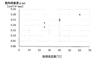
- FIGS. 8A and 8B are diagrams showing the relationship between the SAM processing conditions and the electrical characteristics of the semiconductor. Specifically, FIG. 8A is a diagram showing the relationship between the SAM processing time and the measurement result of the saturation mobility of the semiconductor layer (channel length 5 ⁇ m) in the transistor obtained thereby. Further, FIG. 8B is a diagram showing the relationship between the SAM processing temperature and the measurement result of the saturation mobility of the semiconductor layer in the transistor obtained thereby.
- the temperature of the SAM treatment liquid was fixed at room temperature (25 ° C.), and the immersion time was variously changed to measure the saturation mobility ⁇ sat of the semiconductor layer.
- the saturation mobility ⁇ sat becomes 0.1 [cm 2 / V ⁇ sec] in the immersion time of about 2 minutes, which can be said to be a practical level.
- the saturation mobility ⁇ sat gradually increased, but it was almost saturated in about 30 minutes. From this, it can be said that 2 minutes or more and 30 minutes or less is appropriate as the immersion time when the liquid temperature is about room temperature. From the viewpoint of the electrical characteristics of the transistor to be formed, it is desirable that the immersion time in the SAM treatment is as long as possible within the above range.
- the immersion time was fixed at 30 minutes, and the temperature of the SAM treatment liquid was variously changed to measure the saturation mobility ⁇ sat.
- the higher the processing temperature the larger the saturation mobility ⁇ sat.
- the boiling point of IPA which is a solvent component of the SAM treatment liquid, at atmospheric pressure is about 82 ° C.
- the liquid temperature is at room temperature or higher and below the above boiling point, more preferably 25 ° C. or higher and 60 ° C. or lower. I can say. From the viewpoint of the electrical characteristics of the transistor to be formed, it is desirable that the liquid temperature in the SAM treatment be as high as possible within the above range.
- the mobility (0.25 [cm 2 / V]) is almost the same when the SAM treatment liquid is immersed at room temperature (25 ° C.) for 26 hours and when it is immersed in the treatment liquid at 40 ° C. for 30 minutes. -Sec]) was obtained.
- it is effective to raise the temperature of the SAM treatment liquid.
- the amount of ink used to form the electrodes is preferably as small as possible because it also becomes a source of organic residue.
- the electrode thin to reduce the amount of ink used.
- the above-mentioned electrode forming treatment that is, the method of supporting the electrode pattern PT on the flat plate blanket BL and transferring it to the work Wk is suitable for forming a fine and thin pattern, and is suitable for the above purpose. Further, for example, it is also effective to use an ink in which the content of a high boiling point solvent or a resin component that may remain after firing is suppressed in advance within a range that does not affect the print quality.
- the work Wk is directly SAM processed without cleaning with an acidic solution after the electrode is formed and before the organic semiconductor layer is formed.
- SAM treatment is performed by immersing in a liquid.
- the present invention is not limited to the above-described embodiment, and various modifications other than those described above can be made without departing from the spirit of the present invention.
- the above-described embodiment is an application of the method for manufacturing an organic semiconductor device of the present invention to the manufacture of an organic thin film transistor.
- the manufacturing method of the present invention is not limited to the organic thin film transistor, and can be applied to the manufacturing process of various semiconductor devices.
- the electrode pattern PT is transferred to the work Wk in which the base layer B is formed on the surface of the substrate S.
- the substrate S itself has electrical insulation and has good adhesion to the electrodes formed by the conductive ink, it is not necessary to form the base layer again. That is, in this case, the substrate S itself has a function as the "base material" of the present invention.
- the formation of the electrode pattern PT on the blanket BL surface is realized by patterning using an intaglio or a letterpress.
- the method for forming the electrode pattern is not limited to this, and various methods can be applied.
- the SAM treatment solution in the above embodiment is a solution in which PFBT as a SAM material is dissolved in IPA as an organic solvent.
- the composition of the SAM treatment liquid is not limited to this, and any appropriate composition can be used as long as it can form a SAM film on the surface of the electrode.
- a material containing various benzenethiols as a SAM material and various alcohols as a solvent can be used.
- the electrode transfers an electrode pattern formed on the surface of a transfer medium with ink to a base material. May be formed by. More specifically, an electrode pattern is formed by applying ink to the surface of the transfer medium and patterning with a plate, and the electrode pattern becomes a transfer medium when the transfer medium on which the electrode pattern is formed comes into contact with the base material. It can be configured to be transferred from the substrate to the substrate. According to such a configuration, for example, a method of applying ink to the entire surface of a flat plate-shaped transfer medium with a linear coater or the like can be used, so that a very thin ink film can be uniformly formed. In addition, the electrode pattern can be formed finely according to the dimensions of the high-definition plate. Therefore, by reducing the amount of ink used, the amount of organic matter remaining on the electrodes can be reduced.
- the treatment liquid can contain an organic compound containing a thiol group as a self-assembling material and an alcohol as a solvent.
- an organic compound containing a thiol group as a self-assembling material and an alcohol as a solvent.
- the electrode material may contain silver particles
- the self-assembling material may be benzenethiols
- the solvent may be isopropyl alcohol.
- the base material on which the electrode is formed may be immersed in the treatment liquid so that the electrode is brought into contact with the treatment liquid. According to such a configuration, by bringing the formed electrode into contact with a large amount of the treatment liquid, the ink residual component adhering to the electrode can be effectively transferred from the electrode to the treatment liquid and removed.
- the immersion time of the base material in the treatment liquid may be 2 minutes or more and 30 minutes or less.
- the temperature of the treatment liquid may be 25 ° C. or higher and 60 ° C. or lower. According to the knowledge of the inventor of the present application, it is possible to manufacture a semiconductor device having electrical characteristics equivalent to those in the case of performing acid cleaning by SAM treatment under such processing conditions.
- the method for manufacturing an organic semiconductor device of the present invention may have a configuration in which a base material to which ink is attached is fired to form an electrode, and the base material after firing is immersed in a treatment liquid.
- the electrode can be strengthened by firing.
- the organic component in the ink that remains even after firing can be removed by immersion in the treatment liquid.
- the present invention is particularly effective in manufacturing organic semiconductor elements such as thin film transistors on the surface of substrates such as glass substrates and resin substrates, such as display devices, touch panel devices, and wearable electronic devices.
Landscapes
- Thin Film Transistor (AREA)
- Electroluminescent Light Sources (AREA)
- Physical Deposition Of Substances That Are Components Of Semiconductor Devices (AREA)
Abstract
本発明に係る有機半導体素子の製造方法は、基材の表面に、電極材料を含むインクを用いて電極を形成する工程(ステップS104)と、基材の表面に形成されかつ酸性液による洗浄が施されていない電極に、自己組織化材料を含む処理液を触れさせて、電極の表面に自己組織化材料による自己組織化単分子膜を形成する工程(ステップS106)と、単分子膜を形成された電極に、単分子膜を介して電極と導通する有機半導体層を積層する工程(ステップS107)とを備える。酸洗浄を行わず、かつ電極と半導体層との間の導電性を十分に確保することができる。
Description
この発明は、ガラス板、樹脂板、樹脂シート等の基材上に有機半導体素子、例えば有機薄膜トランジスタを製造する技術に関するものである。
例えば表示装置やタッチパネル装置、ウェアラブル電子装置等を製造することを目的として、ガラス基板や樹脂基板等の基板の表面に薄膜トランジスタなどの薄膜半導体素子を形成するための技術が研究されている。特に近年では、その性能や生産技術の向上が著しく、また材料によっては印刷技術を利用したデバイス作成が可能であるとの観点から、薄膜半導体素子の材料として有機半導体が注目されている。
例えば特許文献1には、金属ナノ粒子を主成分とする導電性インクを基材に塗布することで、薄膜トランジスタ用の電極を製造する技術が記載されている。この技術では、基材の表面に導電性インクを塗布または印刷した後に焼成することで電極を形成し、さらに電極を酸性溶液で洗浄した上で半導体層を積層している。このような工程を含む方法で製造される薄膜トランジスタは、いわゆるトップゲート・ボトムコンタクト型と呼ばれるタイプのものである。
この技術において、酸性溶液による洗浄は、インクに由来する有機物残渣が電極表面に付着して電極と半導体層との間の導電性を阻害することに鑑み、このような残渣を除去する目的で行われている。また特許文献1には、電極表面の改質のために、洗浄後に電極表面を自己組織化膜で修飾する工程を設けてもよい旨が記載されている。
上記従来技術のような、酸性溶液を使用する工程を含む製造プロセスにおいては、酸に対する耐蝕性を有する設備や廃液処理等のコストが、デバイスの製造コストを増大させる要因となる。この問題を解消するため、また環境負荷の低減という観点からも、酸性溶液を使用しない製造プロセスの確立が望まれる。しかしながら、酸性溶液による洗浄(以下、「酸洗浄」と略称する)を行わず、かつ電極と半導体層との間の導電性を十分に確保することのできる製造技術は、これまで確立されるに至っていない。
この発明は上記課題に鑑みなされたものであり、酸洗浄を行わず、かつ電極と半導体層との間の導電性を十分に確保することのできる、有機半導体素子の製造方法を提案することを目的とするものである。
この発明に係る有機半導体素子の製造方法の一の態様は、上記目的を達成するため、基材の表面に、電極材料を含むインクを用いて電極を形成する工程と、前記基材の表面に形成されてから酸性液による洗浄が施されていない前記電極に、自己組織化材料を含む処理液を触れさせて、前記電極の表面に前記自己組織化材料による自己組織化単分子膜を形成する工程と、前記自己組織化単分子膜を形成された前記電極に、前記自己組織化単分子膜を介して前記電極と導通する有機半導体層を積層する工程とを備えている。
本願発明者は、酸性溶液による洗浄工程を含まない製造プロセスを種々検討した結果、上記のように、電極形成後、酸を用いた洗浄を行うことなく、自己組織化単分子膜を形成するための処理液に、電極を直接触れさせることが有効であるとの知見を得た。後述するように、このような製造方法によって製造された有機半導体素子は、インクに由来する有機物残渣の影響も見られず、酸洗浄を伴う製造プロセスにより製造された有機半導体素子と同等の電気的性能を有することが確認されている。
上記のように、本発明によれば、インクにより基材上に形成された電極に対し、自己組織化材料を含む処理液を直接触れさせる。これにより、電極表面に自己組織化単分子膜を形成し、さらに有機半導体層を積層する。このようにすると、酸洗浄を行うことなく、しかも電極と半導体層との間の導電性を十分に確保することのできる有機半導体素子を製造することが可能である。
この発明の前記ならびにその他の目的と新規な特徴は、添付図面を参照しながら次の詳細な説明を読めば、より完全に明らかとなるであろう。ただし、図面は専ら解説のためのものであって、この発明の範囲を限定するものではない。
図1は本発明に係る有機半導体素子の製造方法の一実施形態を示すフローチャートである。また、図2Aないし図2Fはこの製造方法により製造される半導体素子の各工程における構造を示す図である。この製造方法は、例えば半導体基板、ガラス基板、樹脂基板等の種々の平板状の基板に半導体素子を形成するために用いることができる。以下、基板Sとしての例えばガラス板またはポリイミド製シートの表面に、半導体素子の一例としての有機薄膜トランジスタを形成する場合の処理について詳しく説明する。しかしながら、これ以外にも種々の半導体素子の形成のために、下記の方法および装置を用いることができる。
以下の説明では、基板Sに対し各種の機能層が積層されてなる構造体を、各工程における処理対象物たる「ワーク」と称し、符号Wkを付す。このような構造体の構造は製造工程の進行に伴って順次変化するが、それらのいずれについてもワークWkと称するものとする。また、以下のワーク断面図においては、構造上の特徴を明示するため、各層の相対的な厚さは実際のものと必ずしも一致しない。
最初に、処理対象となる基板が適宜の洗浄剤により洗浄され(ステップS101)、基板表面が清浄化される。そして、図2Aに示すように、基板Sの一方表面Saにベース層Bとなる樹脂層が形成される(ステップS102)。ベース層Bについては、例えば硬化状態で電気絶縁性を示す樹脂(例えば各種のポリマー樹脂)の材料を含む溶液を、例えばスピンコート法によって基板表面Saに一様に塗布することにより形成することができる。なお、これに限定されず、一様な層を形成することのできる任意の形成方法を用いてベース層Bを形成することが可能である。
ベース層Bの材料を含む溶液を基板Sに塗布する方法が用いられる場合、形成された塗膜を乾燥硬化させるため、塗布後に焼成処理が行われる(ステップS103)。これにより塗膜が硬化して、基板表面Saに密着したベース層Bが形成される。また、硬化したベース層Bの表面に、新たな層を形成することが可能となる。ベース層Bは、基板S表面を均一かつ安定した絶縁層で被覆するとともに、後工程で形成される各層の形状を安定的に維持する機能を有する。特に、ベース層Bがプライマー層として機能することで、基板Sに対する電極の密着性を向上させる。これにより、後述するウェット処理において電極の崩れや剥落を効果的に防止することが可能である。一方、基板Sの表面Saに電極を直接形成することで十分な密着性を確保できる場合には、ベース層Bの形成を省略することも可能である。
ベース層Bを構成するポリマー樹脂材料としては、例えば、ポリウレタン、ポリイミド、ポリアミドイミド、ポリビニルアルコール、ポリビニルフェノール、ポリエステル、ポリエチレン等を用いることができる。この場合、ポリマーを硬化させるための焼成処理は、例えば120℃、30分程度の条件で行うことができる。例えば、所定の焼成温度に温度調整されたオーブン等の加熱炉内でワークWkを所定時間保持することにより、焼成処理を実行可能である。このような低い焼成温度で硬化するポリマー材料を採用することで、耐熱性の低い樹脂材料も基板として用いることが可能となる。ワークWkは加熱炉内に静置されてもよく、また加熱炉内で搬送されつつ加熱される構成でもよい。
こうして基板Sにベース層Bが積層されたワークWkを基材として、図2Bに示すように、ベース層Bの表面に、有機半導体薄膜トランジスタを構成するソース電極Esおよびドレイン電極Edが形成される(ステップS104)。これらの電極の形成方法については種々の方法を採用可能である。ここではその一例として、予め形成された電極パターンをベース層Bに転写することで電極を形成する、印刷技術を応用した方法について説明する。
図3Aないし図3Dは印刷により電極を製造する方法を模式的に例示する図である。図3Aに示すように、金属粒子(例えば銀)等の導電性材料および溶剤を含む導電性インクにより形成された電極パターンPTが、ガラス板、樹脂板等で形成された転写媒体であるブランケットBLの表面に予め形成される。この例では、ブランケットBLのパターン担持面(図における下面)に、互いに離隔した2つの電極パターンPTが担持されている。これら2つの電極パターンPTは、最終的にそれぞれソース電極およびドレイン電極となって機能する。
ブランケットBLは、パターン担持面をベース層Bの表面に向けた状態で、ワークWkに近接対向配置される。この状態から、図3Bに示すように、パターン担持面とは反対側のブランケットBL表面に、ローラ部材RLが当接される。ローラ部材RLは、ブランケットBLをワークWk側へ押しやりながらブランケットBL表面に沿って転動する。こうすることにより、ブランケットBLに担持された電極パターンPTが、ベース層Bに押し付けられて最終的にベース層Bの表面に転写される。転写後のブランケットBLは、ワークWk近傍から搬出される。
より具体的には、このような電極形成処理は、ブランケットBL上に導電性インクによる電極パターンPTを形成するパターニング工程と、形成された電極パターンPTをワークWkに転写する転写工程とに細分化することができる。以下に説明するように、パターニング工程と転写工程とは同一の処理装置を用いて実行することが可能である。なお、ここに説明する処理については、例えば本願出願人が先に開示した、特開2014-144628号公報に記載された転写装置により実行することが可能である。
図4Aないし図4Dは電極形成処理の過程を示す図である。また、図5Aはパターニング工程を、図5Bは転写工程をそれぞれ示す模式図である。図4A等に示す直交座標系において、XY平面が水平面を表す。また、Z方向が鉛直方向を表し、より具体的には、(+Z)方向が鉛直上向き方向を表す。図4Aないし図4Dを参照しながら、まずパターニング工程について説明する。
電極形成処理を実行する転写装置1では、下面が真空吸着面となった上ステージ11と、中央部が大きく開口する額縁形状を有する下ステージ12とが、それぞれ水平姿勢で互いに近接対向配置されている。下ステージ12の開口121の開口サイズは、上ステージ11の平面サイズよりも大きい。開口121の内部には、図示しない昇降機構により個別に昇降可能に支持された複数の昇降ハンド13が配置されている。
また、開口121の(-X)側端部付近には、Y方向に延びる円柱状または円筒状の押圧ローラ14が配置されている。押圧ローラ14は、支持部材15によりY方向の中心軸回りに回転自在に支持されている。支持部材15は、図示しない駆動機構により、Z方向への昇降およびX方向への走行が可能となっている。押圧ローラ14は、図3Bに示すローラ部材RLに相当する機能を有するものである。
図4Aに示すように、パターニング工程では最初に、所望の電極パターンを反転させた凸パターンを有する版PPが転写装置1に搬入され、上ステージ11にセットされる。上ステージ11は、凸パターンが形成されたパターン形成面を下向きにして版PPを吸着保持する。また、予め導電性インクIkが一様に塗布されたブランケットBLが転写装置1に搬入され、下ステージ12にセットされる。下ステージ12は、導電性インクIkが塗布された面を上向きにして版PPに対向させた状態で、ブランケットBLの周縁部を吸着保持する。
初期状態では、各昇降ハンド13が、その上面が下ステージ12の上面と同じ高さとなるような高さに位置決めされる。これにより、開放された状態のブランケットBL中央部が水平姿勢に維持される。また、押圧ローラ14は、水平方向においては版PPの(-X)側端部の下方、鉛直方向においては上端がブランケットBLの下面から離間した状態となる位置に位置決めされる。
この状態から、支持部材15が押圧ローラ14を上昇させることで、押圧ローラ14がブランケットBLの下面に当接する。押圧ローラ14は、ブランケットBL下面に当接した後も上昇を続ける。こうすることにより、図4Bに示すように、ブランケットBLが押圧ローラ14により押し上げられ、最終的にはブランケットBL上面が版PPの下面に当接する。これにより、ブランケットBL上面に担持されたインクIkが版PPに密着する。さらに押圧ローラ14がブランケットBLを押し上げることで、インクIkが所定の押圧力で版PPに押し付けられる。
この状態で、支持部材15が押圧ローラ14を(+X)方向に移動させる。こうすることで、押圧ローラ14が、ブランケットBLの下面に当接して従動回転しながら(+X)方向へ走行する。これにより、インクIkを介してブランケットBLと版PPとが密着する領域がX方向に広がってゆく。このとき、複数の昇降ハンド13のそれぞれは、図4Cに示すように、走行する押圧ローラ14との干渉を避けるために、支持部材15の移動に伴って順次下降する。
図4Dに示すように、押圧ローラ14が版PPの(+X)側端部直下の終了位置に到達すると、版PP全体がブランケットBLに当接した状態となる。この状態で版PPとブランケットBLとが剥離されると、ブランケットBLに一様塗布されたインクIkのうち凸パターンに対応する部分が版PPに移行し、他の部分がブランケットBL上に残留する。こうすることで、インクIkが凸パターンによりパターニングされ、当該凸パターンの反転パターンが、電極パターンPTとしてブランケットBLに転写される。図5Aは、ブランケットBLに塗布されたインクIkが版PPによりパターニングされ、電極パターンPTが形成される過程を模式的に示した図である。
一方、こうしてブランケットBLに形成された電極パターンPTをワークWkに転写する転写工程は、上記処理における版PPをワークWkに、インクIkを電極パターンPTに読み替えることで説明可能である。すなわち、電極パターンPTが担持されたブランケットBLが下ステージ12により、該パターンを転写されるワークWkが上ステージ11により、それぞれ保持される(図4A)。
そして、押圧ローラ14がブランケットBLを所定の押圧力でワークWkに押し付けながらX方向に走行することで(図4Bないし図4D)、ブランケットBLとワークWkとが電極パターンPTを介して密着する。ワークWkとブランケットBLとを剥離させると、ブランケットBL上の電極パターンPTがワークWkに転写される。図5Bは、基板Sにベース層Bが形成されてなるワークWkに、電極パターンPTが転写される過程(図1のステップS104)を模式的に示した図である。
なお、上記の電極形成処理は、いずれも平板形状を有するブランケットBLとワークWkとを密着させた後剥離することで電極パターンPTをブランケットBLからワークWkに転写させる、平行平板印刷技術を応用したものである。しかしながら、ワークWkに電極パターンPTを形成する方法はこれに限定されず、例えば以下に例示するように種々の方法を適用することが可能である。
図6は電極形成処理の他の態様を示す図である。この処理には転写装置2が用いられる。転写装置2では、円筒状のブランケット胴21の表面にブランケット22が巻回されている。また、電極パターンPTは凹版23上でパターニングされている。ブランケット胴21を所定速度で回転させつつ、凹版23がブランケット22と当接しながら移動する。これにより、凹版23でパターニングされた電極パターンPTがブランケット22に転写される。続いて、ステージ24に載置されたワークWkをブランケットBLに当接させながら、ステージ24が移動する。これにより、ブランケットBL上の電極パターンPTがワークWkに転写される。この方法はオフセット凹版印刷技術に相当するものである。このような方法によっても、ワークWkに電極を形成することが可能である。
また、平板または円筒状のブランケット上でのパターン形成が、他の方法により実行されてもよい。例えば、スクリーン印刷法、インクジェット法等の印刷技術を用いて導電性インクをブランケット表面に部分的に着液させることによって、電極パターンが形成されてもよい。ワークWkに電極パターンPTを形成するという目的においては、これらの印刷技術によりワークWk表面に直接インクを着液させることも考えられる。
図1に戻って処理フローの説明を続ける。転写された電極パターンPTの導電性を得るために、パターン転写後のワークWkに対し焼成処理が行われる(ステップS105)。このときの焼成条件としては、例えば120℃、30分とすることができる。ただし、ステップS103における焼成処理と同一条件であることは必須ではない。この時点でのワークWkは、図2(b)および図3(c)に示すように、電極パターンが硬化することにより、ソース電極Esおよびドレイン電極Edがベース層Bの上面に形成された状態となっている。
次に、形成された電極の表面を改質するSAM処理が実行される(ステップS106)。SAM処理は、電極とそれに積層される半導体層との間における導電性を良好なものとするために、電極表面に自己組織化単分子膜(Self-Assembled Monolayer;SAM)を形成する処理である。SAM処理の原理および方法は公知であるので、ここではウェット処理によりSAM膜を形成する方法の一例を簡単に説明する。
溶媒としてのイソプロピルアルコール(Isopropyl alcohol;IPA)に、自己組織化材料として濃度0.01M程度のペンタフルオロベンゼンチオール(Pentafluorobenzenethiol;PFBT)を溶解させた溶液(以下、「SAM処理液」ということがある)に、ワークWkを少なくとも2分、好ましくは2分以上30分以下の浸漬時間で浸漬する。その後IPAでリンスし乾燥させることにより、PFBTによるSAM膜を形成することが可能である。このようなSAM膜を電極表面に形成することで、この後に積層される有機半導体層と電極との間の電気的接触を低抵抗かつ安定したものとすることができる。SAM処理後のワークWkでは、図2Cに示すように、ワークWkのうち電極Es,Edの露出した表面が、PFBTによる単分子膜Mで覆われた状態となっている。
次に、こうして電極Es,Edが形成されたワークWkの表面を覆うように、有機半導体層が積層される(ステップS107)。有機半導体層は、例えば公知の真空蒸着法を用いて成膜することができる。この時点でのワークWkは、図2Dに示すように、電極Es,Edを覆う単分子膜Mと露出したベース層Bの表面とが、有機半導体層Scにより連続的に覆われた状態となっている。
次に、有機半導体膜Scの表面を覆うゲート絶縁層が形成される(ステップS108)。ゲート絶縁層は、例えば、電気絶縁性を有する材料(例えばパリレン)を、公知の化学的気相成長法(Chemical Vapor Deposition;CVD)を用いて有機半導体膜Scの表面に堆積させて成膜することにより、形成することができる。この時点でのワークWkは、図2Eに示すように、有機半導体層Scの表面全体が、連続的なゲート絶縁層Igにより覆われた状態となっている。
次に、ゲート絶縁層Igの表面にゲート電極が形成される(ステップS109)。例えば、ソース電極Es、ドレイン電極Edの形成と同様の技術でゲート電極を形成することが可能である。すなわち、図3Dに示すように、ゲート電極となる電極パターンPTを担持するブランケットBLをワークWkに近接配置し、ローラ部材RLによりブランケットBLを押圧することで、電極パターンPTをゲート絶縁層Igの表面に転写する。これを焼成処理することで(ステップS110)、図2Fに示すように、ゲート絶縁層Igの表面にゲート電極Egが形成される。また、真空蒸着により金属薄膜を成膜することによっても電極形成が可能である。電極材料としては、例えば金、銀等の金属材料を用いることができる。
以上の一連の処理により、基板S、ベース層B、ソースおよびドレイン電極Es,Ed、有機半導体層Sc、単分子膜M、ゲート絶縁層Ig、ゲート電極Egがこの順番で積層された構造体を形成することができる。このうち、ソースおよびドレイン電極Es,Ed、有機半導体層Sc、ゲート絶縁層Ig、ゲート電極Egが、一体として有機薄膜トランジスタTrとして機能する。基板Sおよびベース層Bは、有機薄膜トランジスタTrを支持する基材として機能する。なお、実際の製造工程においては、上記した構造の有機薄膜トランジスタTrが、1つの基板Sに多数並んだ状態で同時に形成される。
図示を省略しているが、この他に、各電極を配線により接続する工程や、形成された素子の表面を覆う保護層を形成する工程等の追加工程が適宜付加されて、有機薄膜トランジスタTrを含む電子デバイスが完成する。
各層の厚さの一例を示すが、これらの数値に限定されるものではない。ベース層Bの厚さは、例えば100nmである。また、ソースおよびドレイン電極Es,Edの厚さは例えば70nmである。また、有機半導体層Scの厚さは例えば30nmである。また、ソース電極Esとドレイン電極Edとの距離、つまりチャネル長は例えば50μmである。また、ゲート絶縁層Igおよびゲート電極Egの厚さは、それぞれ例えば100nm、200nmである。
上記した製造方法においては、ステップS105の焼成処理と、ステップS106のSAM処理との間に洗浄工程が設けられない。特許文献1に記載された従来技術の有機薄膜トランジスタ製造方法では、導電性インクの塗布および焼成により導電性被膜を形成した後、被膜を酸性溶液で洗浄する。こうしてインクの残留成分等の不要物を除去した上で、必要に応じSAM処理が実行される。一方、本実施形態の製造方法では、酸性溶液による洗浄処理は省かれている。
本願発明者は、種々の製造手順で有機薄膜トランジスタを製造し、その特性を比較検討した。その結果、電極形成後、酸洗浄を行ってからSAM処理を行うケースと、酸洗浄を行わずにSAM処理を行うケースとの間で、得られるトランジスタの電気的特性に大きな差異がないことを見出した。つまり、電極形成後のワークWkを直接SAM処理液に浸漬することによっても、洗浄後にSAM処理液に浸漬する場合と同等の特性を有するトランジスタを製造することが可能である。
図7は洗浄の有無とトランジスタ特性との関係の一例を示す図である。ここではトランジスタの電気的特性を表す指標の例として、特に電極層と半導体層との間における電位障壁の高さに関係する光電子収量を、光電子分光法により計測したときの結果を示す。図7において、横軸はサンプルに照射される入射光のエネルギーを、縦軸は照射を受けてサンプルから放出される光電子の収量を表す。比較するサンプルとしては、酸洗浄およびSAM処理を行わない「未処理」サンプル、従来技術と同様に酸洗浄を行ってからSAM処理を行う「洗浄」サンプル、ならびに、酸洗浄を行わずにSAM処理を行った「未洗浄」サンプルを用いた。洗浄サンプルおよび未洗浄サンプルにおけるSAM処理液への浸漬時間は、いずれも30分である。
図7に示すように、酸洗浄およびSAM処理を行わない未処理サンプルに比べて、洗浄サンプルおよび未洗浄サンプルでは光電子の最大収量が大幅に増大している。また、洗浄サンプルと未洗浄サンプルとの間では収量に有意な差が見られない。もし未洗浄サンプルにおいて電極表面にインク残留成分等の不要物が付着し電荷移動を妨げている場合、洗浄サンプルよりも光電子収量は低下するはずである。しかしながら、計測結果にはそのような傾向は見られず、未洗浄サンプルでも洗浄サンプルと同等の収量が得られている。
このことから、電極形成後のワークWkを洗浄なしで直接SAM処理液に浸漬することによっても、酸洗浄と同等の洗浄効果が得られることがわかる。酸洗浄の工程を省くことができれば、酸性の液体を使用した洗浄を可能とするための設備や、洗浄液の準備および後処理等にかかるコストが不要となる。これにより、デバイスの製造コストを低減することができる。また、洗浄工程を省くことでスループットの向上も期待できる。
SAM処理液への浸漬による洗浄効果を確かめるため、浸漬処理(30分)の前後における電極表面の構成物質を、飛行時間型二次イオン質量分析法(Time-of-Flight Secondary Ion Mass Spectroscopy;TOF-SIMS)を用いて分析した。TOF-SIMS法では、試料表面に一次イオンビームを比較的低照射量で入射させることで試料表面から放出される二次イオンを、その質量の違いによる飛行時間差を利用して分離し検出する。この方法では、試料表面に大きなダメージを与えることなく、表面からごく浅い領域にある物質の分析を行うことが可能である。
分析の結果、浸漬前の電極表面には、シロキサン(より詳しくはジメチルポリシロキサン)、アクリル系樹脂、フッ素系樹脂等の有機物が検出された。これらは浸漬後の電極表面においては減少し、代わって銀、フッ化銀、酸化銀、硫化銀およびPFBTの顕著な増加が見られた。
アクリル系樹脂およびフッ素系樹脂は、電極形成に使用された導電性インクに含まれているバインダーや界面活性剤に由来するものと考えられる。また、シロキサンは、電極パターンの転写に用いられたシリコン樹脂製のブランケットBLに由来するものと考えられる。これらはSAM処理液への浸漬により有意な減少が見られた。
一方、銀およびその化合物は、導電性インクに含まれる銀ナノ粒子に起因するものであり、PFBTはSAM処理液に含まれるSAM材料である。上記の有機物成分の減少とともに銀系化合物の増加が見られる。このことから、浸漬処理によって、自己組織化単分子膜の形成と併せてインクの残留樹脂成分が除去されている、すなわち電極表面が洗浄されていると考えることができる。
なお、比較実験として、SAM材料を含まない有機溶媒、例えばIPAやアセトン等にワークWkを浸漬し電極表面を洗浄することを試みた。しかしながら、これらによっては上記のような洗浄効果は得られなかった。電極表面に対し反応性を有するSAM材料を液中に含むことが、洗浄作用に寄与しているものと考えられる。このような効果を有するSAM材料としては、電極を構成する金属材料(この実施形態では銀)と結び付きやすい特性基、例えばチオール基(-SH)を構造に含むベンゼンチオール類のような有機化合物が使用可能であると考えられる。本例で使用したPFBTは、チオール基を構造に含むベンゼンチオール類の一例である。
図8Aおよび図8BはSAM処理条件と半導体の電気的特性との関係を示す図である。具体的には、図8Aは、SAM処理時間と、それにより得られたトランジスタにおける半導体層(チャネル長5μm)の飽和移動度の計測結果との関係を示す図である。また、図8Bは、SAM処理温度と、それにより得られたトランジスタにおける半導体層の飽和移動度の計測結果との関係を示す図である。
SAM処理液の温度を室温(25℃)に固定し、浸漬時間を種々に変化させて半導体層の飽和移動度μsatを測定した。その結果、図8Aに示すように、2分程度の浸漬時間で飽和移動度μsatは0.1[cm2/V・sec]となり、実用レベルと言える。さらに浸漬時間を長くすると飽和移動度μsatは次第に大きくなるが、30分程度で概ね飽和した。このことから、液温が室温程度であるときの浸漬時間としては、2分以上30分以下が適当であると言える。形成されるトランジスタの電気的特性の観点からは、SAM処理における浸漬時間は、上記範囲内でできるだけ長いことが望ましい。
また、浸漬時間を30分に固定し、SAM処理液の温度を種々に変化させて飽和移動度μsatを測定した。その結果、図8Bに示すように、処理温度が高いほど飽和移動度μsatは大きくなる。SAM処理液の溶媒成分であるIPAの大気圧における沸点が約82℃であることから、液温としては室温以上で上記沸点以下、より好ましくは25℃以上60℃以下の範囲が適当であると言える。形成されるトランジスタの電気的特性の観点からは、SAM処理における液温は上記範囲内でできるだけ高いことが望ましい。
例えば、SAM処理液の温度を室温(25℃)とし26時間浸漬した場合と、40℃の処理液に30分浸漬した場合とで、ほぼ同程度の移動度(0.25[cm2/V・sec])が得られた。デバイスの製造タクトを短くしつつその電気的特性を向上させるためには、SAM処理液の液温を高くすることが効果的である。
このように、電極と半導体層との間の導電性という点においては、導電性インクを用いた電極形成の後、酸洗浄を行わずにSAM処理を行うことによっても、酸洗浄を行った場合と同等の電気的特性を有する半導体素子を形成することが可能であった。ただし、電極表面が多量の有機物に覆われている場合にも、それらを効果的に除去することができるほどの洗浄能力を有するわけではない。このことから、SAM処理前の電極表面に残留するインク成分は少ない方がよい。
したがって、電極の形成に用いられるインクの量は、有機物残渣の発生源ともなるためできるだけ少ない方が好ましい。そのためには、例えば電極を薄くしてインク使用量を少なくすることが考えられる。前述した電極形成処理、すなわち平板ブランケットBLに電極パターンPTを担持させこれをワークWkに転写する方法は、微細かつ薄いパターンを形成するのに適しており、上記目的に好適なものである。また例えば、印刷品質に影響のない範囲で、焼成後に残留し得る高沸点溶媒や樹脂成分の含有量を予め抑えたインクを使用することも有効である。
以上のように、この実施形態では、半導体素子(有機薄膜トランジスタ)の製造プロセスにおいて、電極形成後、有機半導体層を形成する前に、酸性溶液を用いた洗浄を行うことなくワークWkを直接SAM処理液に浸漬することでSAM処理を行う。このように酸洗浄の工程を経ず電極のSAM処理を行う方法によって、酸洗浄後にSAM処理を行う場合と同等の電気的特性を有する半導体素子を製造することが可能である。また、酸洗浄の工程を設けないことで、洗浄液としての酸性溶液が不要となるだけでなく、酸性溶液に耐えるための設備が不要となる。このため、デバイスの製造コストを大きく低減することが可能である。また、洗浄後の廃液処理も不要となることから、環境負荷も小さくすることができる。
なお、本発明は上記した実施形態に限定されるものではなく、その趣旨を逸脱しない限りにおいて上述したもの以外に種々の変更を行うことが可能である。例えば、上記した実施形態は、本発明の有機半導体素子の製造方法を有機薄膜トランジスタの製造に適用したものである。しかしながら、本発明の製造方法は、有機薄膜トランジスタに限定されず、各種の半導体素子の製造プロセスにも適用することが可能である。
また、上記実施形態では、基板Sの表面にベース層Bが形成されたワークWkに対し電極パターンPTが転写される。しかしながら、基板S自体が電気絶縁性を有し、かつ導電性インクにより形成される電極との密着性が良好なものであれば、改めてベース層を形成する必要はない。すなわちこの場合、基板S自体が本発明の「基材」としての機能を有することとなる。
また、上記実施形態では、ブランケットBL表面への電極パターンPTの形成を凹版または凸版を用いたパターニングにより実現している。しかしながら、電極パターンの形成方法はこれに限定されるものではなく、種々の方法を適用可能である。
また、上記実施形態におけるSAM処理液は、SAM材料としてのPFBTを有機溶媒としてのIPAに溶解させた溶液である。しかしながら、SAM処理液の組成はこれに限定されず、電極の表面にSAM膜を形成することのできるものであれば適宜のものを使用可能である。例えば、SAM材料としての各種のベンゼンチオール類と溶媒としての各種のアルコール類とを含むものを用いることができる。
以上、具体的な実施形態を例示して説明してきたように、本発明に係る有機半導体素子の製造方法において、電極は、インクにより転写媒体の表面に形成した電極パターンを基材に転写することにより形成されてよい。より具体的には、転写媒体の表面にインクを塗布して版でパターニングすることにより電極パターンが形成され、電極パターンが形成された転写媒体と基材とが当接することで電極パターンが転写媒体から基材に転写される構成とすることができる。このような構成によれば、例えば平板状の転写媒体にリニアコータなどで全面にインクを塗布する方法を利用可能であるため、非常に薄いインクの膜を均一に形成することができる。また、高精細な版の寸法どおり微細に電極パターンを形成することができる。そのため、インクの使用量を抑えることで、電極への有機物の残留量を低減することができる。
また、処理液は、自己組織化材料としてのチオール基を含む有機化合物と、溶媒としてのアルコールとを含むものとすることができる。このような構成によれば、自己組織化材料がチオール結合により電極材料と結び付きやすいため、電極表面のインク残留成分を除去しつつ単分子膜を形成することができる。より具体的には、電極材料が銀粒子を含み、自己組織化材料がベンゼンチオール類であり、溶媒がイソプロピルアルコールである構成とすることができる。これらの組み合わせにより、電気的特性の良好な半導体素子を形成することが可能である。
また、本発明の有機半導体素子の製造方法では、電極が形成された基材を処理液に浸漬することで電極に処理液を触れさせる構成であってよい。このような構成によれば、形成された電極を大量の処理液に触れさせることで、電極に付着するインク残留成分を電極から処理液に効果的に移行させ除去することができる。
ここで、基材の処理液への浸漬時間は、2分以上30分以下としてよい。また、処理液の温度は、25℃以上60℃以下としてよい。本願発明者の知見によれば、このような処理条件でのSAM処理により、酸洗浄を行う場合と同等の電気的特性を有する半導体素子を製造することが可能である。
また、本発明の有機半導体素子の製造方法は、インクが付着した基材を焼成して電極を形成し、焼成後の基材を処理液に浸漬する構成としてよい。このような構成によれば、焼成によって電極を強固なものとすることができる。焼成後にも残留するインク中の有機物成分については、処理液への浸漬によって除去することができる。
以上、特定の実施例に沿って発明を説明したが、この説明は限定的な意味で解釈されることを意図したものではない。発明の説明を参照すれば、本発明のその他の実施形態と同様に、開示された実施形態の様々な変形例が、この技術に精通した者に明らかとなるであろう。故に、添付の特許請求の範囲は、発明の真の範囲を逸脱しない範囲内で、当該変形例または実施形態を含むものと考えられる。
この発明は、例えば表示装置やタッチパネル装置、ウェアラブル電子装置等、ガラス基板や樹脂基板等の基板の表面への薄膜トランジスタなど有機半導体素子の製造において特に有効なものである。
1,2 転写装置
14 押圧ローラ
21 ブランケット胴
22 ブランケット(転写媒体)
23 凹版
24 ステージ
B ベース層(基材)
BL ブランケット(転写媒体)
Ed ドレイン電極
Eg ゲート電極
Es ソース電極
Ig ゲート絶縁層
Ik インク
PP 凸版
PT 電極パターン
RL ローラ部材
S 基板(基材)
Sc 有機半導体層
Tr 有機半導体薄膜トランジスタ
Wk ワーク
14 押圧ローラ
21 ブランケット胴
22 ブランケット(転写媒体)
23 凹版
24 ステージ
B ベース層(基材)
BL ブランケット(転写媒体)
Ed ドレイン電極
Eg ゲート電極
Es ソース電極
Ig ゲート絶縁層
Ik インク
PP 凸版
PT 電極パターン
RL ローラ部材
S 基板(基材)
Sc 有機半導体層
Tr 有機半導体薄膜トランジスタ
Wk ワーク
Claims (9)
- 基材の表面に、電極材料を含むインクを用いて電極を形成する工程と、
前記基材の表面に形成されてから酸性液による洗浄が施されていない前記電極に、自己組織化材料を含む処理液を触れさせて、前記電極の表面に前記自己組織化材料による自己組織化単分子膜を形成する工程と、
前記自己組織化単分子膜を形成された前記電極に、前記自己組織化単分子膜を介して前記電極と導通する有機半導体層を積層する工程と
を備える有機半導体素子の製造方法。 - 前記電極は、転写媒体の表面に前記インクにより形成した電極パターンを、前記基材に転写することにより形成される請求項1に記載の有機半導体素子の製造方法。
- 前記転写媒体の表面に前記インクを塗布して版でパターニングすることにより前記電極パターンが形成され、
前記電極パターンが形成された前記転写媒体と前記基材とが当接することで、前記電極パターンが前記転写媒体から前記基材に転写される請求項2に記載の有機半導体素子の製造方法。 - 前記処理液は、前記自己組織化材料としての、チオール基を含む有機化合物と、溶媒としてのアルコールとを含む請求項1ないし3のいずれかに記載の有機半導体素子の製造方法。
- 前記電極材料が銀粒子を含み、
前記自己組織化材料がベンゼンチオール類であり、
前記溶媒がイソプロピルアルコールである請求項4に記載の有機半導体素子の製造方法。 - 前記電極が形成された前記基材を前記処理液に浸漬することで、前記電極に前記処理液を触れさせる請求項1ないし5のいずれかに記載の有機半導体素子の製造方法。
- 前記基材の前記処理液への浸漬時間が2分以上30分以下である請求項6に記載の有機半導体素子の製造方法。
- 前記処理液の温度が25℃以上60℃以下である請求項6または7に記載の有機半導体素子の製造方法。
- 前記インクが付着した前記基材を焼成して前記電極を形成し、焼成後の前記基材を前記処理液に浸漬する請求項1ないし8のいずれかに記載の有機半導体素子の製造方法。
Applications Claiming Priority (2)
| Application Number | Priority Date | Filing Date | Title |
|---|---|---|---|
| JP2019-048813 | 2019-03-15 | ||
| JP2019048813A JP2022095997A (ja) | 2019-03-15 | 2019-03-15 | 有機半導体素子の製造方法 |
Publications (1)
| Publication Number | Publication Date |
|---|---|
| WO2020189322A1 true WO2020189322A1 (ja) | 2020-09-24 |
Family
ID=72520936
Family Applications (1)
| Application Number | Title | Priority Date | Filing Date |
|---|---|---|---|
| PCT/JP2020/009571 Ceased WO2020189322A1 (ja) | 2019-03-15 | 2020-03-06 | 有機半導体素子の製造方法 |
Country Status (2)
| Country | Link |
|---|---|
| JP (1) | JP2022095997A (ja) |
| WO (1) | WO2020189322A1 (ja) |
Citations (4)
| Publication number | Priority date | Publication date | Assignee | Title |
|---|---|---|---|---|
| JP2006135109A (ja) * | 2004-11-05 | 2006-05-25 | Seiko Epson Corp | 電子デバイス、電子デバイスの製造方法および電子機器 |
| JP2008060115A (ja) * | 2006-08-29 | 2008-03-13 | Konica Minolta Holdings Inc | 有機薄膜トランジスタの製造方法、及び該製造方法により作製した有機薄膜トランジスタ |
| JP2016058443A (ja) * | 2014-09-05 | 2016-04-21 | Dic株式会社 | 薄膜トランジスタ、トランジスタアレイ、薄膜トランジスタの製造方法及びトランジスタアレイの製造方法 |
| JP2016113434A (ja) * | 2014-12-18 | 2016-06-23 | 住友化学株式会社 | 化合物、該化合物と高分子化合物を含む組成物、該化合物を含む有機薄膜および有機半導体素子 |
-
2019
- 2019-03-15 JP JP2019048813A patent/JP2022095997A/ja active Pending
-
2020
- 2020-03-06 WO PCT/JP2020/009571 patent/WO2020189322A1/ja not_active Ceased
Patent Citations (4)
| Publication number | Priority date | Publication date | Assignee | Title |
|---|---|---|---|---|
| JP2006135109A (ja) * | 2004-11-05 | 2006-05-25 | Seiko Epson Corp | 電子デバイス、電子デバイスの製造方法および電子機器 |
| JP2008060115A (ja) * | 2006-08-29 | 2008-03-13 | Konica Minolta Holdings Inc | 有機薄膜トランジスタの製造方法、及び該製造方法により作製した有機薄膜トランジスタ |
| JP2016058443A (ja) * | 2014-09-05 | 2016-04-21 | Dic株式会社 | 薄膜トランジスタ、トランジスタアレイ、薄膜トランジスタの製造方法及びトランジスタアレイの製造方法 |
| JP2016113434A (ja) * | 2014-12-18 | 2016-06-23 | 住友化学株式会社 | 化合物、該化合物と高分子化合物を含む組成物、該化合物を含む有機薄膜および有機半導体素子 |
Also Published As
| Publication number | Publication date |
|---|---|
| JP2022095997A (ja) | 2022-06-29 |
Similar Documents
| Publication | Publication Date | Title |
|---|---|---|
| JP4960434B2 (ja) | 有機発光表示装置及びその製造方法 | |
| JP5341966B2 (ja) | パターン転写方法及びパターン転写装置、これを適用したフレキシブルディスプレイパネル、フレキシブル太陽電池、電子本、薄膜トランジスター、電磁波遮蔽シート、フレキシブル印刷回路基板 | |
| US20070105396A1 (en) | High resolution structures defined by brush painting fluid onto surface energy patterned substrates | |
| TWI777064B (zh) | 轉印基板 | |
| TWI524565B (zh) | Production method of transistor and transistor | |
| KR102065901B1 (ko) | 수지기판 적층체 및 전자 디바이스의 제조방법 | |
| CN106885839B (zh) | 一种通过将分析物富集到尖端提高解吸电离效率的方法 | |
| US9459526B2 (en) | Process for manufacturing a self-assembled injection monolayer | |
| GB2427509A (en) | Organic electronic device fabrication by micro-embossing | |
| KR101226086B1 (ko) | 패턴 제조 방법 및 패턴 전사 장치 | |
| WO2020189322A1 (ja) | 有機半導体素子の製造方法 | |
| CN113488373B (zh) | 一种干法制备单层二维半导体阵列的方法 | |
| KR101164061B1 (ko) | 패턴 제조 방법 및 패턴 전사 장치, 이를 적용한 플렉서블 디스플레이 패널, 플렉서블 태양전지, 전자책, 박막 트랜지스터, 전자파 차폐시트, 플렉서블 인쇄회로기판 | |
| KR20200057389A (ko) | 대면적 열보조 패턴 전사 프린팅 방법 | |
| JP2007201056A (ja) | 薄膜トランジスタ及びその製造方法 | |
| US20100192372A1 (en) | Method of disposing electronic device on electrode formed on substrate to connect electrically the electronic device and the electrode | |
| JPWO2019208241A1 (ja) | 有機薄膜トランジスタ用の電極形成方法および電極形成装置、有機薄膜トランジスタの製造方法ならびに有機薄膜トランジスタ | |
| KR20170122307A (ko) | 박리 조력층의 전사 과정을 포함하는 플렉시블 정보 표시 소자의 제조 방법 | |
| JP2015205452A (ja) | 機能性素子の製造方法および印刷装置 | |
| KR20190052784A (ko) | 후면전극 기판 및 이의 제조방법 | |
| JP2017224739A (ja) | 能動素子、および能動素子の製造方法 | |
| JP6620556B2 (ja) | 機能材料の積層方法及び機能材料積層体 | |
| Sakata et al. | Anti-sticking effect of organic dielectric formed by electrodeposition in microelectromechanical-system structures | |
| WO2019208206A1 (ja) | 有機半導体装置及び有機半導体装置の製造方法 | |
| HK40008366A (en) | Transfer substrate |
Legal Events
| Date | Code | Title | Description |
|---|---|---|---|
| 121 | Ep: the epo has been informed by wipo that ep was designated in this application |
Ref document number: 20774291 Country of ref document: EP Kind code of ref document: A1 |
|
| NENP | Non-entry into the national phase |
Ref country code: DE |
|
| 122 | Ep: pct application non-entry in european phase |
Ref document number: 20774291 Country of ref document: EP Kind code of ref document: A1 |
|
| NENP | Non-entry into the national phase |
Ref country code: JP |