WO2020189179A1 - 受光素子および受光素子の製造方法ならびに撮像装置 - Google Patents
受光素子および受光素子の製造方法ならびに撮像装置 Download PDFInfo
- Publication number
- WO2020189179A1 WO2020189179A1 PCT/JP2020/007047 JP2020007047W WO2020189179A1 WO 2020189179 A1 WO2020189179 A1 WO 2020189179A1 JP 2020007047 W JP2020007047 W JP 2020007047W WO 2020189179 A1 WO2020189179 A1 WO 2020189179A1
- Authority
- WO
- WIPO (PCT)
- Prior art keywords
- diffusion region
- light receiving
- receiving element
- impurity diffusion
- layer
- Prior art date
- Legal status (The legal status is an assumption and is not a legal conclusion. Google has not performed a legal analysis and makes no representation as to the accuracy of the status listed.)
- Ceased
Links
Images















Classifications
-
- H—ELECTRICITY
- H10—SEMICONDUCTOR DEVICES; ELECTRIC SOLID-STATE DEVICES NOT OTHERWISE PROVIDED FOR
- H10D—INORGANIC ELECTRIC SEMICONDUCTOR DEVICES
- H10D64/00—Electrodes of devices having potential barriers
- H10D64/01—Manufacture or treatment
- H10D64/011—Manufacture or treatment of electrodes ohmically coupled to a semiconductor
-
- H—ELECTRICITY
- H10—SEMICONDUCTOR DEVICES; ELECTRIC SOLID-STATE DEVICES NOT OTHERWISE PROVIDED FOR
- H10F—INORGANIC SEMICONDUCTOR DEVICES SENSITIVE TO INFRARED RADIATION, LIGHT, ELECTROMAGNETIC RADIATION OF SHORTER WAVELENGTH OR CORPUSCULAR RADIATION
- H10F30/00—Individual radiation-sensitive semiconductor devices in which radiation controls the flow of current through the devices, e.g. photodetectors
- H10F30/20—Individual radiation-sensitive semiconductor devices in which radiation controls the flow of current through the devices, e.g. photodetectors the devices having potential barriers, e.g. phototransistors
- H10F30/21—Individual radiation-sensitive semiconductor devices in which radiation controls the flow of current through the devices, e.g. photodetectors the devices having potential barriers, e.g. phototransistors the devices being sensitive to infrared, visible or ultraviolet radiation
- H10F30/22—Individual radiation-sensitive semiconductor devices in which radiation controls the flow of current through the devices, e.g. photodetectors the devices having potential barriers, e.g. phototransistors the devices being sensitive to infrared, visible or ultraviolet radiation the devices having only one potential barrier, e.g. photodiodes
- H10F30/225—Individual radiation-sensitive semiconductor devices in which radiation controls the flow of current through the devices, e.g. photodetectors the devices having potential barriers, e.g. phototransistors the devices being sensitive to infrared, visible or ultraviolet radiation the devices having only one potential barrier, e.g. photodiodes the potential barrier working in avalanche mode, e.g. avalanche photodiodes
-
- H—ELECTRICITY
- H10—SEMICONDUCTOR DEVICES; ELECTRIC SOLID-STATE DEVICES NOT OTHERWISE PROVIDED FOR
- H10F—INORGANIC SEMICONDUCTOR DEVICES SENSITIVE TO INFRARED RADIATION, LIGHT, ELECTROMAGNETIC RADIATION OF SHORTER WAVELENGTH OR CORPUSCULAR RADIATION
- H10F30/00—Individual radiation-sensitive semiconductor devices in which radiation controls the flow of current through the devices, e.g. photodetectors
- H10F30/20—Individual radiation-sensitive semiconductor devices in which radiation controls the flow of current through the devices, e.g. photodetectors the devices having potential barriers, e.g. phototransistors
- H10F30/21—Individual radiation-sensitive semiconductor devices in which radiation controls the flow of current through the devices, e.g. photodetectors the devices having potential barriers, e.g. phototransistors the devices being sensitive to infrared, visible or ultraviolet radiation
- H10F30/22—Individual radiation-sensitive semiconductor devices in which radiation controls the flow of current through the devices, e.g. photodetectors the devices having potential barriers, e.g. phototransistors the devices being sensitive to infrared, visible or ultraviolet radiation the devices having only one potential barrier, e.g. photodiodes
- H10F30/225—Individual radiation-sensitive semiconductor devices in which radiation controls the flow of current through the devices, e.g. photodetectors the devices having potential barriers, e.g. phototransistors the devices being sensitive to infrared, visible or ultraviolet radiation the devices having only one potential barrier, e.g. photodiodes the potential barrier working in avalanche mode, e.g. avalanche photodiodes
- H10F30/2255—Individual radiation-sensitive semiconductor devices in which radiation controls the flow of current through the devices, e.g. photodetectors the devices having potential barriers, e.g. phototransistors the devices being sensitive to infrared, visible or ultraviolet radiation the devices having only one potential barrier, e.g. photodiodes the potential barrier working in avalanche mode, e.g. avalanche photodiodes in which the active layers form heterostructures, e.g. SAM structures
-
- H—ELECTRICITY
- H10—SEMICONDUCTOR DEVICES; ELECTRIC SOLID-STATE DEVICES NOT OTHERWISE PROVIDED FOR
- H10F—INORGANIC SEMICONDUCTOR DEVICES SENSITIVE TO INFRARED RADIATION, LIGHT, ELECTROMAGNETIC RADIATION OF SHORTER WAVELENGTH OR CORPUSCULAR RADIATION
- H10F39/00—Integrated devices, or assemblies of multiple devices, comprising at least one element covered by group H10F30/00, e.g. radiation detectors comprising photodiode arrays
- H10F39/10—Integrated devices
- H10F39/12—Image sensors
-
- H—ELECTRICITY
- H10—SEMICONDUCTOR DEVICES; ELECTRIC SOLID-STATE DEVICES NOT OTHERWISE PROVIDED FOR
- H10F—INORGANIC SEMICONDUCTOR DEVICES SENSITIVE TO INFRARED RADIATION, LIGHT, ELECTROMAGNETIC RADIATION OF SHORTER WAVELENGTH OR CORPUSCULAR RADIATION
- H10F39/00—Integrated devices, or assemblies of multiple devices, comprising at least one element covered by group H10F30/00, e.g. radiation detectors comprising photodiode arrays
- H10F39/80—Constructional details of image sensors
-
- H—ELECTRICITY
- H10—SEMICONDUCTOR DEVICES; ELECTRIC SOLID-STATE DEVICES NOT OTHERWISE PROVIDED FOR
- H10F—INORGANIC SEMICONDUCTOR DEVICES SENSITIVE TO INFRARED RADIATION, LIGHT, ELECTROMAGNETIC RADIATION OF SHORTER WAVELENGTH OR CORPUSCULAR RADIATION
- H10F71/00—Manufacture or treatment of devices covered by this subclass
-
- H—ELECTRICITY
- H10—SEMICONDUCTOR DEVICES; ELECTRIC SOLID-STATE DEVICES NOT OTHERWISE PROVIDED FOR
- H10F—INORGANIC SEMICONDUCTOR DEVICES SENSITIVE TO INFRARED RADIATION, LIGHT, ELECTROMAGNETIC RADIATION OF SHORTER WAVELENGTH OR CORPUSCULAR RADIATION
- H10F77/00—Constructional details of devices covered by this subclass
- H10F77/10—Semiconductor bodies
- H10F77/14—Shape of semiconductor bodies; Shapes, relative sizes or dispositions of semiconductor regions within semiconductor bodies
- H10F77/146—Superlattices; Multiple quantum well structures
-
- H—ELECTRICITY
- H10—SEMICONDUCTOR DEVICES; ELECTRIC SOLID-STATE DEVICES NOT OTHERWISE PROVIDED FOR
- H10F—INORGANIC SEMICONDUCTOR DEVICES SENSITIVE TO INFRARED RADIATION, LIGHT, ELECTROMAGNETIC RADIATION OF SHORTER WAVELENGTH OR CORPUSCULAR RADIATION
- H10F77/00—Constructional details of devices covered by this subclass
- H10F77/10—Semiconductor bodies
- H10F77/14—Shape of semiconductor bodies; Shapes, relative sizes or dispositions of semiconductor regions within semiconductor bodies
- H10F77/148—Shapes of potential barriers
-
- H—ELECTRICITY
- H10—SEMICONDUCTOR DEVICES; ELECTRIC SOLID-STATE DEVICES NOT OTHERWISE PROVIDED FOR
- H10P—GENERIC PROCESSES OR APPARATUS FOR THE MANUFACTURE OR TREATMENT OF DEVICES COVERED BY CLASS H10
- H10P14/00—Formation of materials, e.g. in the shape of layers or pillars
- H10P14/40—Formation of materials, e.g. in the shape of layers or pillars of conductive or resistive materials
-
- H—ELECTRICITY
- H10—SEMICONDUCTOR DEVICES; ELECTRIC SOLID-STATE DEVICES NOT OTHERWISE PROVIDED FOR
- H10W—GENERIC PACKAGES, INTERCONNECTIONS, CONNECTORS OR OTHER CONSTRUCTIONAL DETAILS OF DEVICES COVERED BY CLASS H10
- H10W20/00—Interconnections in chips, wafers or substrates
- H10W20/01—Manufacture or treatment
-
- H—ELECTRICITY
- H10—SEMICONDUCTOR DEVICES; ELECTRIC SOLID-STATE DEVICES NOT OTHERWISE PROVIDED FOR
- H10W—GENERIC PACKAGES, INTERCONNECTIONS, CONNECTORS OR OTHER CONSTRUCTIONAL DETAILS OF DEVICES COVERED BY CLASS H10
- H10W20/00—Interconnections in chips, wafers or substrates
- H10W20/40—Interconnections external to wafers or substrates, e.g. back-end-of-line [BEOL] metallisations or vias connecting to gate electrodes
Definitions
- FIG. 8A It is sectional drawing which shows the process following FIG. 8B. It is sectional drawing which shows the process following FIG. 8C. It is sectional drawing which shows the process following FIG. 8D. It is sectional drawing which shows the process following FIG. 8E. It is sectional drawing which shows the process following FIG.
- the photoelectric conversion layer 14 In the light receiving element 1, light is incident on the photoelectric conversion layer 14 from the light incident surface S1 of the element substrate 10 via the passivation film 16, the second electrode 15, and the carrier transfer layer 13B.
- the signal charge photoelectrically converted by the photoelectric conversion layer 14 moves through the first electrode 11 and the wiring layer 10W, and is read out by the reading circuit board 20. The configuration of each part will be described below.
- the photoelectric conversion layer 14 is provided in common to all pixels P, for example.
- the photoelectric conversion layer 14 is provided between the carrier transfer layer 13A and the carrier transfer layer 13B, and is in contact with them.
- the photoelectric conversion layer 14 absorbs light having a predetermined wavelength to generate a signal charge, and is made of, for example, a compound semiconductor material such as an i-type III-V semiconductor. Examples of the compound semiconductor material constituting the photoelectric conversion layer 14 include i-type InGaAs (indium gallium arsenide).
- In the photoelectric conversion layer 14 for example, photoelectric conversion of light having a wavelength in the visible region to the short infrared region is performed.
- the passivation film 16 covers the second electrode 15 from the light incident surface S1 side.
- the passivation film 16 may have an antireflection function.
- silicon nitride (SiN), aluminum oxide (Al 2 O 3 ), silicon oxide (SiO 2 ), tantalum oxide (Ta 2 O 3 ) and the like can be used.
- the insulating film 17 is provided between the non-doped layer 12 and the embedded layer 18, and covers the non-doped layer 12, the carrier transfer layer 13A, the photoelectric conversion layer 14, the end faces of the carrier transfer layer 13B, and the end faces of the second electrode 15. , In contact with the passivation film 16 in the peripheral region R2.
- the insulating film 17 is composed of, for example, an oxide such as silicon oxide (SiO 2 ) or aluminum oxide (Al 2 O 3 ).
- the insulating film 17 may be formed by a laminated structure composed of a plurality of films.
- the surface of the embedded layer 18 on the joint surface S2 side is flattened, and in the peripheral region R2, the wiring layer 10W is provided on the surface of the flattened embedded layer 18.
- an inorganic insulating material such as silicon oxide (SiO X ), silicon nitride (SiN), silicon oxynitride (SiON), carbon-containing silicon oxide (SiOC), and silicon carbide (SiC) is used. Can be done.
- the opening H2 is provided, for example, at a position closer to the tip end E than the opening H1.
- the opening H2 penetrates the passivation film 16, the embedding layer 18, and the wiring layer 10W, and reaches the pad electrode (pad electrode 22P described later) of the reading circuit board 20.
- An electrical connection between the outside and the light receiving element 1 is made through the opening H2.
- the openings H1 and H2 do not have to reach the read circuit board 20.
- the openings H1 and H2 may reach the wiring of the wiring layer 10W, and this wiring may be connected to the wiring 22CB and the pad electrode 22P of the reading circuit board 20.
- the openings H1 and H2 may penetrate the adhesive layer B described later.
- the wiring layer 10W is provided over the element region R1 and the peripheral region R2, and has a junction surface S2 with the read circuit board 20.
- the bonding surface S2 of the element substrate 10 is provided in the element region R1 and the peripheral region R2.
- the bonding surface S2 of the element region R1 and the bonding surface S2 of the peripheral region R2 form the same plane. There is.
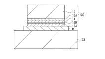
- the semiconductor layer 10S is etched to a predetermined size according to the mark on the temporary substrate 33. As a result, a plurality of chip-state semiconductor layers 10S are formed.
- the reading circuit board 20 is attached to the temporary board 33 with the wiring layer 10W in between. At this time, the wiring layer 20W is formed in advance on the reading circuit board 20.
- the wiring layer 20W of the reading circuit board 20 has a contact electrode 22E and a dummy electrode 22ED.
- the contact electrode 22E and the dummy electrode of the wiring layer 20W are attached.
- the 22ED, the contact electrode 19E of the wiring layer 10W, and the dummy electrode 19ED are CuCu bonded.
- the adhesive layer B and the like are also removed to expose the surface of the semiconductor layer 10S. At this time, the unnecessary layer of the semiconductor layer 10S may be removed. Further, the insulating layer 33IA or the insulating film 17 other than the opening of the semiconductor layer 10S may be partially left, or the embedded layer 18 may be dug halfway.
- the second electrode 15 and the passivation are placed on the surface of the semiconductor layer 10S (the surface opposite to the surface on which the wiring layer 10W is provided) exposed by removing the temporary substrate 33.
- the film 16 is formed in this order.
- the opening H1 and the conductive film 15B are formed.
- the second electrode 15 and the reading circuit board 20 are electrically connected.
- the light receiving element 1 when light (for example, light having a wavelength in the visible region and an infrared region) is incident on the photoelectric conversion layer 14 via the passivation film 16, the second electrode 15, and the carrier transfer layer 13B, this light is photoelectrically converted. It is absorbed in layer 14. As a result, holes and electron pairs are generated (photoelectrically converted) in the photoelectric conversion layer 14.
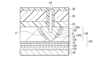
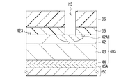
- the depletion layer spreads between the convex portion C of the first diffusion region 12A and the carrier transfer layer 13A composed of n-type InP, and the high electric field region Is formed. In the high field region, carriers are multiplied by avalanche multiplication.
- the first diffusion region 12A has a diffusion shape having an inflection point X, and penetrates the second diffusion region 12B in the stacking direction (for example, the Z-axis direction) of the semiconductor layer 10S. It has a convex portion C. This makes it possible to concentrate the electric field on the convex portion C.
- the contact area between the non-doped layer 12 and the first electrode 11 increases, and the contact resistance decreases. Therefore, it is possible to improve the transfer efficiency.
- FIG. 4 schematically shows a cross-sectional configuration of a light receiving element (light receiving element 2) according to the second embodiment of the present disclosure.
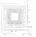
- FIG. 5 schematically shows the planar configuration of the light receiving element 2 shown in FIG. Note that FIG. 4 shows the cross-sectional structure of the line II-II'shown in FIG.
- the light receiving element 2 is applied to an infrared sensor or the like using a compound semiconductor material such as a group III-V semiconductor, and is, for example, a visible region (for example, 380 nm or more and less than 780 nm) to a short infrared region (for example, 780 nm). It is a PN photodiode having a photoelectric conversion function for light having a wavelength (more than 2400 nm).
- the diffusion region 42X has a first diffusion region 42A and a second diffusion region 42B having a lower impurity concentration than the first diffusion region 42A, and the second diffusion region 42B is It has a configuration provided around the first diffusion region 42A.
- the first diffusion region 42A corresponds to a specific example of the "first impurity diffusion region” of the present disclosure
- the second diffusion region 42B corresponds to a specific example of the "second impurity diffusion region" of the present disclosure. ..
- the photoelectric conversion layer 43 In the light receiving element 2, light is incident on the photoelectric conversion layer 43 from the light incident surface S3 of the element substrate 40 via the passivation film 16, the second electrode 45, and the second contact layer 44.
- the signal charge photoelectrically converted by the photoelectric conversion layer 43 moves via the first electrode 41 and the wiring layer 10W, and is read out by the reading circuit board 20. The configuration of each part will be described below.
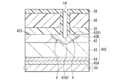
- the first diffusion region 42A has a diffusion shape having an inflection point X, and for example, the convex portion C in the stacking direction (for example, the Z-axis direction) of the layers 42, 43, 44 constituting the semiconductor layer 40S. It is preferable to have.
- the convex portion C penetrates the second diffusion region 42B. That is, the diffusion region 42X forms a gentle impurity concentration gradient in the horizontal direction (XY plane direction) and a steep impurity concentration gradient in the vertical direction (Z-axis direction). Defects that cause dark current are dominated by the surface of the first contact layer 42.
- the electric field is concentrated on the convex portion C and the electric field in the lateral direction of the diffusion region 42X is relaxed, so that the surface of the first contact layer 42 The probability of dark current generation through defects is reduced.
- the diffusion region 42X is provided with a groove t in the first diffusion region 42A, similarly to the diffusion region 12X in the first embodiment.
- the first electrode 41 is embedded in the groove t.
- the photoelectric conversion layer 43 is provided in common to all pixels P, for example.
- the photoelectric conversion layer 43 is provided between the first contact layer 42 and the second contact layer 44, and is in contact with them.
- the photoelectric conversion layer 43 absorbs light having a predetermined wavelength to generate a signal charge, and is made of, for example, a compound semiconductor material such as an i-type III-V group semiconductor.
- Examples of the compound semiconductor material constituting the photoelectric conversion layer 43 include InGaAs (indium gallium arsenide), InAsSb (indium arsenide antimony), InAs (indium arsenide), InSb (indium antimony) and HgCdTe (mercury cadmium tellurium).
- the photoelectric conversion layer 43 may be formed of Ge (germanium). In the photoelectric conversion layer 43, for example, photoelectric conversion of light having a wavelength in the visible region to the short infrared region is performed.
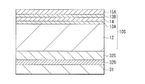
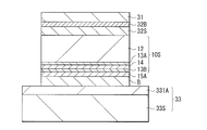
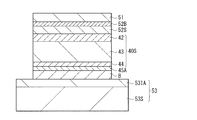
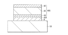
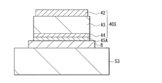
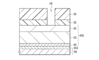
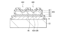
- the light receiving element 2 can be manufactured, for example, as follows. 8A to 8K show the manufacturing process of the light receiving element 1 in the order of the process.
- the n-type InP constituting the first contact layer 42, the n-type InGaAs constituting the photoelectric conversion layer 43, and the n-type InP constituting the second contact layer 44 are epitaxially grown in this order. Let me do it.
- the temporary substrate 53 has, for example, an insulating layer (insulating layer 53IA) and a substrate 53S.
- the insulating layer 53IA is arranged, for example, between the adhesive layer B and the substrate 53S.
- insulating layer 53IA is arranged, for example, between the adhesive layer B and the substrate 53S.
- a substrate having a diameter larger than that of the growth substrate 51 is used, and for the substrate 53S, for example, a silicon (Si) substrate is used.
- the diameter of the temporary substrate 53 is, for example, 8 inches to 12 inches.
- the small-diameter growth substrate 51 By joining the small-diameter growth substrate 51 to the large-diameter temporary substrate 53, it becomes possible to use various devices for the large-diameter substrate when forming the element substrate 40.
- the junction between the read circuit board 20 and the element substrate 40 can be made into a CuCu junction, and the pixel P can be miniaturized.
- the growth substrate 51 may be bonded to the temporary substrate 53 by plasma activation bonding, room temperature bonding, bonding using an adhesive (adhesive bonding), or the like.
- the wafer-shaped semiconductor layer 40S is bonded to the temporary substrate 53.
- the thickness of the temporary substrate 53 is, for example, several hundred ⁇ m.
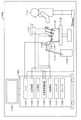
- the endoscope 11100 is composed of a lens barrel 11101 in which a region having a predetermined length from the tip is inserted into the body cavity of the patient 11132, and a camera head 11102 connected to the base end of the lens barrel 11101.
- the endoscope 11100 configured as a so-called rigid mirror having a rigid barrel 11101 is illustrated, but the endoscope 11100 may be configured as a so-called flexible mirror having a flexible barrel. Good.
- the image processing unit 11412 performs various image processing on the image signal which is the RAW data transmitted from the camera head 11102.
- the control unit 11413 performs various controls related to the imaging of the surgical site and the like by the endoscope 11100 and the display of the captured image obtained by the imaging of the surgical site and the like. For example, the control unit 11413 generates a control signal for controlling the drive of the camera head 11102.
- the transmission cable 11400 that connects the camera head 11102 and CCU11201 is an electric signal cable that supports electric signal communication, an optical fiber that supports optical communication, or a composite cable thereof.
- the communication was performed by wire using the transmission cable 11400, but the communication between the camera head 11102 and the CCU11201 may be performed wirelessly.
- the technique according to the present disclosure may be applied to other, for example, a microscopic surgery system.
- the technology according to the present disclosure can be applied to various products.
- the technology according to the present disclosure is realized as a device mounted on a moving body of any kind such as an automobile, an electric vehicle, a hybrid electric vehicle, a motorcycle, a bicycle, a personal mobility, an airplane, a drone, a ship, and a robot. You may.
- FIG. 12 is a block diagram showing a schematic configuration example of a vehicle control system, which is an example of a moving body control system to which the technique according to the present disclosure can be applied.
- the vehicle control system 12000 includes a plurality of electronic control units connected via the communication network 12001.
- the vehicle control system 12000 includes a drive system control unit 12010, a body system control unit 12020, an outside information detection unit 12030, an in-vehicle information detection unit 12040, and an integrated control unit 12050.
- a microcomputer 12051, an audio image output unit 12052, and an in-vehicle network I / F (Interface) 12053 are shown as a functional configuration of the integrated control unit 12050.
- the drive system control unit 12010 controls the operation of the device related to the drive system of the vehicle according to various programs.
- the drive system control unit 12010 provides a driving force generator for generating the driving force of the vehicle such as an internal combustion engine or a driving motor, a driving force transmission mechanism for transmitting the driving force to the wheels, and a steering angle of the vehicle. It functions as a control device such as a steering mechanism for adjusting and a braking device for generating braking force of the vehicle.
- the body system control unit 12020 controls the operation of various devices mounted on the vehicle body according to various programs.
- the body system control unit 12020 functions as a keyless entry system, a smart key system, a power window device, or a control device for various lamps such as headlamps, back lamps, brake lamps, blinkers or fog lamps.
- the body system control unit 12020 may be input with radio waves transmitted from a portable device that substitutes for the key or signals of various switches.
- the body system control unit 12020 receives inputs of these radio waves or signals and controls a vehicle door lock device, a power window device, a lamp, and the like.
- the imaging unit 12031 is an optical sensor that receives light and outputs an electric signal according to the amount of the light received.
- the image pickup unit 12031 can output an electric signal as an image or can output it as distance measurement information. Further, the light received by the imaging unit 12031 may be visible light or invisible light such as infrared light.
- the in-vehicle information detection unit 12040 detects the in-vehicle information.
- a driver state detection unit 12041 that detects the driver's state is connected to the in-vehicle information detection unit 12040.
- the driver state detection unit 12041 includes, for example, a camera that images the driver, and the in-vehicle information detection unit 12040 determines the degree of fatigue or concentration of the driver based on the detection information input from the driver state detection unit 12041. It may be calculated, or it may be determined whether the driver is dozing.
- the microcomputer 12051 calculates the control target value of the driving force generator, the steering mechanism, or the braking device based on the information inside and outside the vehicle acquired by the vehicle exterior information detection unit 12030 or the vehicle interior information detection unit 12040, and the drive system control unit.
- a control command can be output to 12010.
- the microcomputer 12051 realizes ADAS (Advanced Driver Assistance System) functions including vehicle collision avoidance or impact mitigation, follow-up driving based on inter-vehicle distance, vehicle speed maintenance driving, vehicle collision warning, vehicle lane deviation warning, and the like. It is possible to perform cooperative control for the purpose of.
- ADAS Advanced Driver Assistance System
- the microcomputer 12051 controls the driving force generator, the steering mechanism, the braking device, and the like based on the information around the vehicle acquired by the vehicle exterior information detection unit 12030 or the vehicle interior information detection unit 12040. It is possible to perform coordinated control for the purpose of automatic driving that runs autonomously without depending on the operation.
- the microcomputer 12051 can output a control command to the body system control unit 12020 based on the information outside the vehicle acquired by the vehicle exterior information detection unit 12030.
- the microcomputer 12051 controls the headlamps according to the position of the preceding vehicle or the oncoming vehicle detected by the external information detection unit 12030, and performs coordinated control for the purpose of anti-glare such as switching the high beam to the low beam. It can be carried out.
- the audio image output unit 12052 transmits the output signal of at least one of the audio and the image to the output device capable of visually or audibly notifying the passenger of the vehicle or the outside of the vehicle.
- an audio speaker 12061, a display unit 12062, and an instrument panel 12063 are exemplified as output devices.
- the display unit 12062 may include, for example, at least one of an onboard display and a heads-up display.
- the imaging unit 12031 includes imaging units 12101, 12102, 12103, 12104, and 12105.
- FIG. 13 shows an example of the photographing range of the imaging units 12101 to 12104.
- the imaging range 12111 indicates the imaging range of the imaging unit 12101 provided on the front nose
- the imaging ranges 12112 and 12113 indicate the imaging ranges of the imaging units 12102 and 12103 provided on the side mirrors, respectively
- the imaging range 12114 indicates the imaging range of the imaging units 12102 and 12103.
- the imaging range of the imaging unit 12104 provided on the rear bumper or the back door is shown. For example, by superimposing the image data captured by the imaging units 12101 to 12104, a bird's-eye view image of the vehicle 12100 as viewed from above can be obtained.
- At least one of the imaging units 12101 to 12104 may have a function of acquiring distance information.
- at least one of the image pickup units 12101 to 12104 may be a stereo camera composed of a plurality of image pickup elements, or may be an image pickup element having pixels for phase difference detection.
- the microcomputer 12051 has a distance to each three-dimensional object within the imaging range 12111 to 12114 based on the distance information obtained from the imaging units 12101 to 12104, and a temporal change of this distance (relative velocity with respect to the vehicle 12100). By obtaining it can. Further, the microcomputer 12051 can set an inter-vehicle distance to be secured in front of the preceding vehicle in advance, and can perform automatic braking control (including follow-up stop control), automatic acceleration control (including follow-up start control), and the like. In this way, it is possible to perform coordinated control for the purpose of automatic driving or the like in which the vehicle runs autonomously without depending on the operation of the driver.
- automatic braking control including follow-up stop control
- automatic acceleration control including follow-up start control
- the microcomputer 12051 converts three-dimensional object data related to a three-dimensional object into two-wheeled vehicles, ordinary vehicles, large vehicles, pedestrians, utility poles, and other three-dimensional objects based on the distance information obtained from the imaging units 12101 to 12104. It can be classified and extracted and used for automatic avoidance of obstacles. For example, the microcomputer 12051 distinguishes obstacles around the vehicle 12100 into obstacles that can be seen by the driver of the vehicle 12100 and obstacles that are difficult to see. Then, the microcomputer 12051 determines the collision risk indicating the risk of collision with each obstacle, and when the collision risk is equal to or higher than the set value and there is a possibility of collision, the microcomputer 12051 via the audio speaker 12061 or the display unit 12062. By outputting an alarm to the driver and performing forced deceleration and avoidance steering via the drive system control unit 12010, driving support for collision avoidance can be provided.
- At least one of the imaging units 12101 to 12104 may be an infrared camera that detects infrared rays.
- the microcomputer 12051 can recognize a pedestrian by determining whether or not a pedestrian is present in the captured image of the imaging units 12101 to 12104.
- pedestrian recognition includes, for example, a procedure for extracting feature points in an image captured by an imaging unit 12101 to 12104 as an infrared camera, and pattern matching processing for a series of feature points indicating the outline of an object to determine whether or not the pedestrian is a pedestrian. It is done by the procedure to determine.
- the audio image output unit 12052 When the microcomputer 12051 determines that a pedestrian is present in the captured images of the imaging units 12101 to 12104 and recognizes the pedestrian, the audio image output unit 12052 outputs a square contour line for emphasizing the recognized pedestrian.
- the display unit 12062 is controlled so as to superimpose and display. Further, the audio image output unit 12052 may control the display unit 12062 so as to display an icon or the like indicating a pedestrian at a desired position.
- the above is an example of a vehicle control system to which the technology according to the present disclosure can be applied.
- the technique according to the present disclosure can be applied to the imaging unit 12031 among the configurations described above. By applying the technique according to the present disclosure to the imaging unit 12031, it is possible to obtain a photographed image that is easier to see, and thus it is possible to reduce driver fatigue.
- the light receiving elements 1 and 2 described in the present embodiment and the like can be applied to electronic devices such as surveillance cameras, biometric authentication systems and thermography.
- Surveillance cameras are, for example, those of night vision systems (night vision).
- night vision systems night vision
- the light receiving element 1 or the light receiving element 2 By applying the light receiving element 1 or the light receiving element 2 to the surveillance camera, it becomes possible to recognize pedestrians, animals, and the like at night from a distance.
- the light receiving element 1 or the light receiving element 2 is applied as an in-vehicle camera, it is not easily affected by the headlights and the weather. For example, a photographed image can be obtained without being affected by smoke, fog, or the like. Further, the shape of the object can be recognized.
- thermography non-contact temperature measurement becomes possible. Thermography can also detect temperature distribution and heat generation.
- the light receiving elements 1 and 2 are also applicable to electronic devices that detect flames, moisture, gas, and the like.
- the element substrate for example, the element substrate 10
- the read circuit board 20 may be bonded via bumps.
- the signal charge is a hole
- the signal charge may be an electron
- the diffusion region may contain n-type impurities.
- effect described in the above-described embodiment or the like is an example, and may be another effect, or may further include another effect.
- the present technology can also have the following configurations.
- an impurity diffusion region in which the impurity concentration changes stepwise is provided on one surface of the semiconductor layer containing the compound semiconductor material, so that the electric field in the lateral direction can be relaxed. it can. Therefore, it is possible to reduce the dark current.
- a sidewall is formed in the opening to form a sidewall.
- a groove is formed in the first impurity diffusion region by etching to form a groove.
- Method of manufacturing the element 17.
Landscapes
- Solid State Image Pick-Up Elements (AREA)
- Light Receiving Elements (AREA)
Abstract
Description
1.第1の実施の形態(段階的に変化する亜鉛拡散領域を有する受光素子の例)
1-1.受光素子の構成
1-2.受光素子の製造方法
1-3.受光素子の動作
1-4.作用・効果
2.第2の実施の形態(撮像装置を構成する受光素子(PNフォトダイオード)に適用した例)
2-1.受光素子の構成
2-2.受光素子の製造方法
2-3.受光素子の動作
2-4.作用・効果
3.適用例
4.応用例
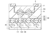
図1は、本開示の第1の実施の形態に係る受光素子(受光素子1)の断面構成を模式的に表したものである。図2は、図1に示した受光素子1の平面構成を模式的に表したものである。なお、図1は、図2に示したI-I’線における断面構成を表している。この受光素子1は、例えばIII-V族半導体等の化合物半導体材料を用いた、いわゆるアバランシェフォトダイオード(APD)であり、赤外線センサ等に適用されるものである。この受光素子1には、例えば2次元配置された複数の受光単位領域P(画素P)が設けられている。
受光素子1は、例えば、可視領域(例えば380nm以上780nm未満)~短赤外領域(例えば780nm以上2400nm未満)の波長の光に対して、光電変換機能を有するものであり、例えば、中央部の素子領域R1と、素子領域R1の外側に設けられ、素子領域R1を囲む周辺領域R2とを有している(図2)。受光素子1は、素子基板10と、読出回路基板20とが積層された積層構造を有する。素子基板10は光入射面(光入射面S1)と、光入射面S1と対向すると共に、読出回路基板20と接合される接合面(接合面S2)とを有する。素子基板10は、読出回路基板20に近い位置から配線層10W、第1電極11、ノンドープ層12、キャリア転送層13A、光電変換層14、キャリア転送層13Bおよび第2電極15をこの順に有している。ノンドープ層12、キャリア転送層13A,13Bおよび光電変換層14は、例えば、複数の画素Pに対して共通の半導体層10Sを構成しており、ノンドープ層12の面12S2には、画素P毎に、不純物が拡散した拡散領域12Xが設けられている。本実施の形態の受光素子1では、拡散領域12Xは、第1拡散領域12Aと、第1拡散領域12Aよりも不純物濃度の低い第2拡散領域12Bとを有し、第2拡散領域12Bは、第1拡散領域12Aの周囲に設けられた構成となっている。この第1拡散領域12Aが本開示の「第1の不純物拡散領域」の一具体例に相当し、第2拡散領域12Bが本開示の「第2の不純物拡散領域」の一具体例に相当する。
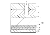
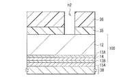
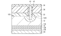
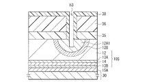
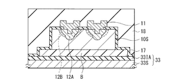
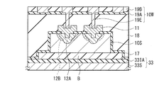
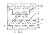
受光素子1は、例えば次のようにして製造することができる。図3A~図3Sは、受光素子1の製造工程を工程順に表したものである。
受光素子1では、パッシベーション膜16、第2電極15およびキャリア転送層13Bを介して、光電変換層14へ光(例えば可視領域および赤外領域の波長の光)が入射すると、この光が光電変換層14において吸収される。これにより、光電変換層14では正孔(ホール)および電子の対が発生する(光電変換される)。このとき、例えば第1電極11に所定の電圧が印加されると、第1拡散領域12Aの凸部Cとn型のInPからなるキャリア転送層13Aとの間に空乏層が広がり、高電界領域が形成される。高電界領域ではアバランシェ増倍によりキャリアが増倍される。高電界領域に生じたキャリア(電荷)のうちの一方の電荷(例えば正孔)は、信号電荷としてノンドープ層12内の拡散領域12Xに移動し、拡散領域12Xから第1電極11へ収集される。この信号電荷が、コンタクト電極19E,22Eを通じて半導体基板21に移動し、画素P毎に読み出される。
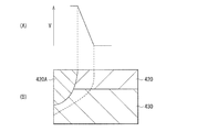
本実施の形態の受光素子1では、半導体層10S(具体的には、ノンドープ層12)の第1電極11と接する面に、不純物濃度が段階的に変化する拡散領域12Xが設けられている。これにより、例えば、横方向の電界が緩和される。以下、これについて説明する。
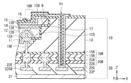
図4は、本開示の第2の実施の形態に係る受光素子(受光素子2)の断面構成を模式的に表したものである。図5は、図4に示した受光素子2の平面構成を模式的に表したものである。なお、図4は、図5に示したII-II’線における断面構成を表している。この受光素子2は、例えばIII-V族半導体等の化合物半導体材料を用いた赤外線センサ等に適用されるものであり、例えば、可視領域(例えば380nm以上780nm未満)~短赤外領域(例えば780nm以上2400nm未満)の波長の光に、光電変換機能を有するPNフォトダイオードである。
受光素子2は、例えば、中央部の素子領域R1と、素子領域R1の外側に設けられ、素子領域R1を囲む周辺領域R2とを有している(図5)。受光素子2は、上記第1の実施の形態における受光素子1と同様に、素子基板40と、読出回路基板20とが積層された積層構造を有する。素子基板40は光入射面(光入射面S3)と、光入射面S3と対向すると共に、読出回路基板20と接合される接合面(接合面S4)とを有する。素子基板40は、読出回路基板20に近い位置から配線層10W、第1電極41、第1コンタクト層42、光電変換層43および第2コンタクト層44および第2電極45をこの順に有している。第1コンタクト層42、光電変換層43および第2コンタクト層44は、例えば、複数の画素Pに対して共通の半導体層40Sを構成しており、第1コンタクト層42の面42S2には、画素P毎に、不純物が拡散した拡散領域42Xが設けられている。本実施の形態の受光素子2では、拡散領域42Xは、第1拡散領域42Aと、第1拡散領域42Aよりも不純物濃度の低い第2拡散領域42Bとを有し、第2拡散領域42Bは、第1拡散領域42Aの周囲に設けられた構成となっている。この第1拡散領域42Aが本開示の「第1の不純物拡散領域」の一具体例に相当し、第2拡散領域42Bが本開示の「第2の不純物拡散領域」の一具体例に相当する。
受光素子2は、例えば次のようにして製造することができる。図8A~図8Kは、受光素子1の製造工程を工程順に表したものである。
受光素子2では、パッシベーション膜16、第2電極45および第2コンタクト層44を介して、光電変換層43へ光(例えば可視領域および赤外領域の波長の光)が入射すると、この光が光電変換層43において吸収される。これにより、光電変換層43では正孔(ホール)および電子の対が発生する(光電変換される)。このとき、例えば第1電極41に所定の電圧が印加されると、光電変換層43に電位勾配が生じ、発生した電荷のうち一方の電荷(例えば正孔)が、信号電荷として拡散領域42Xに移動し、拡散領域42Xから第1電極41へ収集される。この信号電荷が、コンタクト電極19E,22Eを通じて半導体基板21に移動し、画素P毎に読み出される。
本実施の形態の受光素子2は、半導体層40S(具体的には、第1コンタクト層42)の第1電極41と接する面に、不純物濃度が段階的に変化する拡散領域42Xが設けられている。この拡散領域42Xは、例えば、第1拡散領域42Aと、第1拡散領域42Aよりも不純物濃度の低い第2拡散領域42Bを有し、第2拡散領域42Bは、第1拡散領域42Aの周囲に設けられた構成となっている。これにより、例えば、横方向の電界が緩和される。
(適用例1)
上記実施の形態等において説明した受光素子1(または、受光素子2)は、例えば、撮像素子に適用される。この撮像素子は、例えば赤外線イメージセンサである。
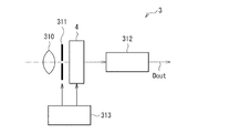
上述の受光素子1,2は、例えば赤外領域を撮像可能なカメラ等、様々なタイプの電子機器(撮像装置)に適用することができる。図9に、その一例として、電子機器3の概略構成を示す。この電子機器3は、例えば静止画または動画を撮影可能なカメラであり、例えば受光素子1により構成された撮像素子4と、光学系(光学レンズ)310と、シャッタ装置311と、撮像素子4およびシャッタ装置311を駆動する駆動部313と、信号処理部312とを有する。
(応用例1.内視鏡手術システム)
本開示に係る技術は、様々な製品へ応用することができる。例えば、本開示に係る技術は、内視鏡手術システムに適用されてもよい。
本開示に係る技術は、様々な製品へ応用することができる。例えば、本開示に係る技術は、自動車、電気自動車、ハイブリッド電気自動車、自動二輪車、自転車、パーソナルモビリティ、飛行機、ドローン、船舶、ロボット等のいずれかの種類の移動体に搭載される装置として実現されてもよい。
(1)
化合物半導体材料を含む半導体層と、
前記半導体層の一の面に設けられた第1の不純物拡散領域と、
前記第1の不純物拡散領域の周囲に設けられると共に、前記第1の不純物拡散領域よりも不純物濃度が低い第2の不純物拡散領域と
を備えた受光素子。
(2)
前記第1の不純物拡散領域は変曲点を持つ拡散形状を有する、前記(1)に記載の受光素子。
(3)
前記第1の不純物拡散領域は、前記第2の不純物拡散領域を貫通する凸部を有する、前記(1)または(2)に記載の受光素子。
(4)
更に、前記半導体層の前記一の面側に設けられると共に、前記半導体層に電気的に接続された第1電極と、
前記半導体層を間にして前記第1電極に対向する第2電極とを有する、前記(1)乃至(3)のうちのいずれかに記載の受光素子。
(5)
前記半導体層は、前記第1の不純物拡散領域に溝を有し、
前記溝には、前記第1電極の一部が埋設されている、前記(4)に記載の受光素子。
(6)
前記半導体層は、前記一の面側から順に積層され、導電型または構成材料の異なる第1の半導体層および第2の半導体層を有し、
前記第1の不純物拡散領域および前記第2の不純物拡散領域は、前記第1の半導体層に設けられている、前記(1)乃至(5)のうちのいずれかに記載の受光素子。
(7)
前記第1の不純物拡散領域は、前記第2の不純物拡散領域を貫通する凸部を有し、
前記凸部は、前記第1の半導体層内に形成されている、前記(6)に記載の受光素子。
(8)
前記第1の不純物拡散領域は、前記第2の不純物拡散領域を貫通する凸部を有し、
前記凸部は、一部が前記第2の半導体層内に突出している、前記(6)に記載の受光素子。
(9)
前記第1の不純物拡散領域および前記第2の不純物拡散領域には亜鉛(Zn)が拡散されている、前記(1)乃至(8)のうちのいずれかに記載の受光素子。
(10)
前記化合物半導体材料は、赤外領域の波長の光を吸収する、前記(1)乃至(9)のうちのいずれかに記載の受光素子。
(11)
前記化合物半導体材料はIII-V族半導体である、前記(1)乃至(10)のうちのいずれかに記載の受光素子。
(12)
前記化合物半導体材料は、InGaAs,InAsSb,InAs,InSbおよびHgCdTeのうちのいずれか1つである、前記(1)乃至(11)のうちのいずれかに記載の受光素子。
(13)
前記半導体層は多重量子井戸構造を有する、前記(1)乃至(12)のうちのいずれかに記載の受光素子。
(14)
複数の受光素子がアレイ状に配置された素子領域を有し、
前記受光素子は、
化合物半導体材料を含む半導体層と、
前記半導体層の一の面に設けられた第1の不純物拡散領域と、
前記第1の不純物拡散領域の周囲に設けられると共に、前記第1の不純物拡散領域よりも不純物濃度が低い第2の不純物拡散領域と
を備えた撮像装置。
(15)
化合物半導体材料を含む半導体層を形成し、
前記半導体層の一の面上に開口を有するマスク層を形成し、
前記開口を介して不純物を拡散して前記半導体層の前記一の面に第1の不純物拡散領域を形成し、
アニール処理にて前記第1の不純物拡散領域よりも不純物濃度の低い第2の不純物拡散領域を前記第1の不純物拡散領域の周囲に形成する
受光素子の製造方法。
(16)
前記開口内にサイドウォールを形成し、
エッチングにより前記第1の不純物拡散領域内に溝を形成し、
前記アニール処理後に前記溝を介して前記第1の不純物拡散領域に再度不純物を拡散して前記第1の不純物拡散領域を、変曲点を持つ拡散形状とする、前記(15)に記載の受光素子の製造方法。
(17)
前記溝内に金属材料を埋設し、前記受光素子と電気的に接続された第1電極を形成する、前記(16)に記載の受光素子の製造方法。
Claims (17)
- 化合物半導体材料を含む半導体層と、
前記半導体層の一の面に設けられた第1の不純物拡散領域と、
前記第1の不純物拡散領域の周囲に設けられると共に、前記第1の不純物拡散領域よりも不純物濃度が低い第2の不純物拡散領域と
を備えた受光素子。 - 前記第1の不純物拡散領域は変曲点を持つ拡散形状を有する、請求項1に記載の受光素子。
- 前記第1の不純物拡散領域は、前記第2の不純物拡散領域を貫通する凸部を有する、請求項1に記載の受光素子。
- 更に、前記半導体層の前記一の面側に設けられると共に、前記半導体層に電気的に接続された第1電極と、
前記半導体層を間にして前記第1電極に対向する第2電極とを有する、請求項1に記載の受光素子。 - 前記半導体層は、前記第1の不純物拡散領域に溝を有し、
前記溝には、前記第1電極の一部が埋設されている、請求項4に記載の受光素子。 - 前記半導体層は、前記一の面側から順に積層され、導電型または構成材料の異なる第1の半導体層および第2の半導体層を有し、
前記第1の不純物拡散領域および前記第2の不純物拡散領域は、前記第1の半導体層に設けられている、請求項1に記載の受光素子。 - 前記第1の不純物拡散領域は、前記第2の不純物拡散領域を貫通する凸部を有し、
前記凸部は、前記第1の半導体層内に形成されている、請求項6に記載の受光素子。 - 前記第1の不純物拡散領域は、前記第2の不純物拡散領域を貫通する凸部を有し、
前記凸部は、一部が前記第2の半導体層内に突出している、請求項6に記載の受光素子。 - 前記第1の不純物拡散領域および前記第2の不純物拡散領域には亜鉛(Zn)が拡散されている、請求項1に記載の受光素子。
- 前記化合物半導体材料は、赤外領域の波長の光を吸収する、請求項1に記載の受光素子。
- 前記化合物半導体材料はIII-V族半導体である、請求項1に記載の受光素子。
- 前記化合物半導体材料は、InGaAs,InAsSb,InAs,InSbおよびHgCdTeのうちのいずれか1つである、請求項1に記載の受光素子。
- 前記半導体層は多重量子井戸構造を有する、請求項1に記載の受光素子。
- 複数の受光素子がアレイ状に配置された素子領域を有し、
前記受光素子は、
化合物半導体材料を含む半導体層と、
前記半導体層の一の面に設けられた第1の不純物拡散領域と、
前記第1の不純物拡散領域の周囲に設けられると共に、前記第1の不純物拡散領域よりも不純物濃度が低い第2の不純物拡散領域と
を備えた撮像装置。 - 化合物半導体材料を含む半導体層を形成し、
前記半導体層の一の面上に開口を有するマスク層を形成し、
前記開口を介して不純物を拡散して前記半導体層の前記一の面に第1の不純物拡散領域を形成し、
アニール処理にて前記第1の不純物拡散領域よりも不純物濃度の低い第2の不純物拡散領域を前記第1の不純物拡散領域の周囲に形成する
受光素子の製造方法。 - 前記開口内にサイドウォールを形成し、
エッチングにより前記第1の不純物拡散領域内に溝を形成し、
前記アニール処理後に前記溝を介して前記第1の不純物拡散領域に再度不純物を拡散して前記第1の不純物拡散領域を、変曲点を持つ拡散形状とする、請求項15に記載の受光素子の製造方法。 - 前記溝内に金属材料を埋設し、前記受光素子と電気的に接続された第1電極を形成する、請求項16に記載の受光素子の製造方法。
Priority Applications (3)
| Application Number | Priority Date | Filing Date | Title |
|---|---|---|---|
| US17/440,939 US11804561B2 (en) | 2019-03-20 | 2020-02-21 | Light receiving element, method of manufacturing light receiving element, and imaging apparatus |
| JP2021507126A JP7524160B2 (ja) | 2019-03-20 | 2020-02-21 | 受光素子の製造方法 |
| CN202080012286.9A CN113366656B (zh) | 2019-03-20 | 2020-02-21 | 光接收元件、光接收元件的制造方法以及摄像装置 |
Applications Claiming Priority (2)
| Application Number | Priority Date | Filing Date | Title |
|---|---|---|---|
| JP2019052687 | 2019-03-20 | ||
| JP2019-052687 | 2019-03-20 |
Publications (1)
| Publication Number | Publication Date |
|---|---|
| WO2020189179A1 true WO2020189179A1 (ja) | 2020-09-24 |
Family
ID=72520202
Family Applications (1)
| Application Number | Title | Priority Date | Filing Date |
|---|---|---|---|
| PCT/JP2020/007047 Ceased WO2020189179A1 (ja) | 2019-03-20 | 2020-02-21 | 受光素子および受光素子の製造方法ならびに撮像装置 |
Country Status (4)
| Country | Link |
|---|---|
| US (1) | US11804561B2 (ja) |
| JP (1) | JP7524160B2 (ja) |
| CN (1) | CN113366656B (ja) |
| WO (1) | WO2020189179A1 (ja) |
Cited By (2)
| Publication number | Priority date | Publication date | Assignee | Title |
|---|---|---|---|---|
| JP2022112911A (ja) * | 2021-01-22 | 2022-08-03 | キヤノン株式会社 | 光電変換装置、その製造方法及び機器 |
| WO2024034017A1 (ja) * | 2022-08-09 | 2024-02-15 | ソニーセミコンダクタソリューションズ株式会社 | 受光素子及び光検出装置 |
Families Citing this family (1)
| Publication number | Priority date | Publication date | Assignee | Title |
|---|---|---|---|---|
| CN118983327A (zh) * | 2024-10-22 | 2024-11-19 | 浙江珏芯微电子有限公司 | 一种制冷红外探测器的制备方法 |
Citations (9)
| Publication number | Priority date | Publication date | Assignee | Title |
|---|---|---|---|---|
| JPS57159072A (en) * | 1981-03-25 | 1982-10-01 | Nippon Telegr & Teleph Corp <Ntt> | Manufacture of avalanche photodiode |
| JPH01144687A (ja) * | 1987-11-30 | 1989-06-06 | Nec Corp | 半導体受光素子 |
| JPH02159775A (ja) * | 1988-12-14 | 1990-06-19 | Toshiba Corp | 半導体受光素子及びその製造方法 |
| JPH09232617A (ja) * | 1996-02-21 | 1997-09-05 | Fujitsu Ltd | 赤外線検知素子及びその製造方法 |
| JP2001274451A (ja) * | 2000-03-27 | 2001-10-05 | Toshiba Corp | 半導体撮像素子およびその製造方法 |
| JP2007080920A (ja) * | 2005-09-12 | 2007-03-29 | Mitsubishi Electric Corp | アバランシェフォトダイオード |
| JP2012069941A (ja) * | 2010-09-16 | 2012-04-05 | Commissariat A L'energie Atomique & Aux Energies Alternatives | 多層のバイスペクトルフォトダイオード検出器 |
| KR101393083B1 (ko) * | 2013-01-11 | 2014-05-09 | 한국과학기술원 | 애벌랜치 포토다이오드 및 그 제조방법 |
| WO2018174090A1 (ja) * | 2017-03-22 | 2018-09-27 | ソニーセミコンダクタソリューションズ株式会社 | 撮像装置及び信号処理装置 |
Family Cites Families (8)
| Publication number | Priority date | Publication date | Assignee | Title |
|---|---|---|---|---|
| KR100840098B1 (ko) * | 2007-07-04 | 2008-06-19 | 삼성에스디아이 주식회사 | 유기전계발광 소자 및 그의 제조 방법 |
| JP4662188B2 (ja) * | 2008-02-01 | 2011-03-30 | 住友電気工業株式会社 | 受光素子、受光素子アレイおよびそれらの製造方法 |
| EP2278632A4 (en) * | 2008-04-30 | 2013-11-27 | Mitsubishi Electric Corp | PHOTOVOLTAIC ASSEMBLY AND METHOD FOR THE PRODUCTION THEREOF |
| JP2010114320A (ja) * | 2008-11-07 | 2010-05-20 | Panasonic Corp | 半導体装置 |
| WO2015015808A1 (ja) * | 2013-08-01 | 2015-02-05 | 三菱電機株式会社 | 炭化珪素半導体装置およびその製造方法 |
| JP6743035B2 (ja) * | 2015-10-05 | 2020-08-19 | ソニーセミコンダクタソリューションズ株式会社 | 撮像装置、製造方法 |
| JP2017098424A (ja) * | 2015-11-25 | 2017-06-01 | ソニー株式会社 | 半導体装置、製造方法 |
| JP6688653B2 (ja) * | 2016-03-30 | 2020-04-28 | エイブリック株式会社 | 半導体装置および半導体装置の製造方法 |
-
2020
- 2020-02-21 US US17/440,939 patent/US11804561B2/en active Active
- 2020-02-21 JP JP2021507126A patent/JP7524160B2/ja active Active
- 2020-02-21 CN CN202080012286.9A patent/CN113366656B/zh active Active
- 2020-02-21 WO PCT/JP2020/007047 patent/WO2020189179A1/ja not_active Ceased
Patent Citations (9)
| Publication number | Priority date | Publication date | Assignee | Title |
|---|---|---|---|---|
| JPS57159072A (en) * | 1981-03-25 | 1982-10-01 | Nippon Telegr & Teleph Corp <Ntt> | Manufacture of avalanche photodiode |
| JPH01144687A (ja) * | 1987-11-30 | 1989-06-06 | Nec Corp | 半導体受光素子 |
| JPH02159775A (ja) * | 1988-12-14 | 1990-06-19 | Toshiba Corp | 半導体受光素子及びその製造方法 |
| JPH09232617A (ja) * | 1996-02-21 | 1997-09-05 | Fujitsu Ltd | 赤外線検知素子及びその製造方法 |
| JP2001274451A (ja) * | 2000-03-27 | 2001-10-05 | Toshiba Corp | 半導体撮像素子およびその製造方法 |
| JP2007080920A (ja) * | 2005-09-12 | 2007-03-29 | Mitsubishi Electric Corp | アバランシェフォトダイオード |
| JP2012069941A (ja) * | 2010-09-16 | 2012-04-05 | Commissariat A L'energie Atomique & Aux Energies Alternatives | 多層のバイスペクトルフォトダイオード検出器 |
| KR101393083B1 (ko) * | 2013-01-11 | 2014-05-09 | 한국과학기술원 | 애벌랜치 포토다이오드 및 그 제조방법 |
| WO2018174090A1 (ja) * | 2017-03-22 | 2018-09-27 | ソニーセミコンダクタソリューションズ株式会社 | 撮像装置及び信号処理装置 |
Cited By (3)
| Publication number | Priority date | Publication date | Assignee | Title |
|---|---|---|---|---|
| JP2022112911A (ja) * | 2021-01-22 | 2022-08-03 | キヤノン株式会社 | 光電変換装置、その製造方法及び機器 |
| JP7702788B2 (ja) | 2021-01-22 | 2025-07-04 | キヤノン株式会社 | 光電変換装置、その製造方法及び機器 |
| WO2024034017A1 (ja) * | 2022-08-09 | 2024-02-15 | ソニーセミコンダクタソリューションズ株式会社 | 受光素子及び光検出装置 |
Also Published As
| Publication number | Publication date |
|---|---|
| CN113366656B (zh) | 2025-03-25 |
| CN113366656A (zh) | 2021-09-07 |
| JP7524160B2 (ja) | 2024-07-29 |
| JPWO2020189179A1 (ja) | 2020-09-24 |
| US11804561B2 (en) | 2023-10-31 |
| US20220165896A1 (en) | 2022-05-26 |
Similar Documents
| Publication | Publication Date | Title |
|---|---|---|
| US10991745B2 (en) | Semiconductor device, method of manufacturing the same, and electronic apparatus | |
| US11476285B2 (en) | Light-receiving device, imaging device, and electronic apparatus | |
| KR102653046B1 (ko) | 수광 소자 및 전자 기기 | |
| JP6979974B2 (ja) | 受光素子の製造方法 | |
| JPWO2020137283A1 (ja) | 半導体素子 | |
| JP7660642B2 (ja) | 半導体素子 | |
| JP7524160B2 (ja) | 受光素子の製造方法 | |
| JP2021089978A (ja) | 半導体素子および電子機器 | |
| JP2021089979A (ja) | 半導体素子および電子機器 | |
| JPWO2020137282A1 (ja) | 撮像素子および電子機器 | |
| JP7653788B2 (ja) | 撮像素子および電子機器 | |
| US20260059875A1 (en) | Photodetection device |
Legal Events
| Date | Code | Title | Description |
|---|---|---|---|
| 121 | Ep: the epo has been informed by wipo that ep was designated in this application |
Ref document number: 20772965 Country of ref document: EP Kind code of ref document: A1 |
|
| ENP | Entry into the national phase |
Ref document number: 2021507126 Country of ref document: JP Kind code of ref document: A |
|
| NENP | Non-entry into the national phase |
Ref country code: DE |
|
| 122 | Ep: pct application non-entry in european phase |
Ref document number: 20772965 Country of ref document: EP Kind code of ref document: A1 |
|
| WWG | Wipo information: grant in national office |
Ref document number: 202080012286.9 Country of ref document: CN |