WO2020189047A1 - 表示装置 - Google Patents
表示装置 Download PDFInfo
- Publication number
- WO2020189047A1 WO2020189047A1 PCT/JP2020/003536 JP2020003536W WO2020189047A1 WO 2020189047 A1 WO2020189047 A1 WO 2020189047A1 JP 2020003536 W JP2020003536 W JP 2020003536W WO 2020189047 A1 WO2020189047 A1 WO 2020189047A1
- Authority
- WO
- WIPO (PCT)
- Prior art keywords
- light emitting
- emitting element
- pixel
- electrode
- pixel electrode
- Prior art date
- Legal status (The legal status is an assumption and is not a legal conclusion. Google has not performed a legal analysis and makes no representation as to the accuracy of the status listed.)
- Ceased
Links
Images








Classifications
-
- H—ELECTRICITY
- H10—SEMICONDUCTOR DEVICES; ELECTRIC SOLID-STATE DEVICES NOT OTHERWISE PROVIDED FOR
- H10W—GENERIC PACKAGES, INTERCONNECTIONS, CONNECTORS OR OTHER CONSTRUCTIONAL DETAILS OF DEVICES COVERED BY CLASS H10
- H10W90/00—Package configurations
-
- H—ELECTRICITY
- H10—SEMICONDUCTOR DEVICES; ELECTRIC SOLID-STATE DEVICES NOT OTHERWISE PROVIDED FOR
- H10H—INORGANIC LIGHT-EMITTING SEMICONDUCTOR DEVICES HAVING POTENTIAL BARRIERS
- H10H29/00—Integrated devices, or assemblies of multiple devices, comprising at least one light-emitting semiconductor element covered by group H10H20/00
- H10H29/30—Active-matrix LED displays
- H10H29/49—Interconnections, e.g. wiring lines or terminals
-
- G—PHYSICS
- G09—EDUCATION; CRYPTOGRAPHY; DISPLAY; ADVERTISING; SEALS
- G09G—ARRANGEMENTS OR CIRCUITS FOR CONTROL OF INDICATING DEVICES USING STATIC MEANS TO PRESENT VARIABLE INFORMATION
- G09G3/00—Control arrangements or circuits, of interest only in connection with visual indicators other than cathode-ray tubes
- G09G3/20—Control arrangements or circuits, of interest only in connection with visual indicators other than cathode-ray tubes for presentation of an assembly of a number of characters, e.g. a page, by composing the assembly by combination of individual elements arranged in a matrix no fixed position being assigned to or needed to be assigned to the individual characters or partial characters
-
- G—PHYSICS
- G09—EDUCATION; CRYPTOGRAPHY; DISPLAY; ADVERTISING; SEALS
- G09G—ARRANGEMENTS OR CIRCUITS FOR CONTROL OF INDICATING DEVICES USING STATIC MEANS TO PRESENT VARIABLE INFORMATION
- G09G3/00—Control arrangements or circuits, of interest only in connection with visual indicators other than cathode-ray tubes
- G09G3/20—Control arrangements or circuits, of interest only in connection with visual indicators other than cathode-ray tubes for presentation of an assembly of a number of characters, e.g. a page, by composing the assembly by combination of individual elements arranged in a matrix no fixed position being assigned to or needed to be assigned to the individual characters or partial characters
- G09G3/22—Control arrangements or circuits, of interest only in connection with visual indicators other than cathode-ray tubes for presentation of an assembly of a number of characters, e.g. a page, by composing the assembly by combination of individual elements arranged in a matrix no fixed position being assigned to or needed to be assigned to the individual characters or partial characters using controlled light sources
- G09G3/30—Control arrangements or circuits, of interest only in connection with visual indicators other than cathode-ray tubes for presentation of an assembly of a number of characters, e.g. a page, by composing the assembly by combination of individual elements arranged in a matrix no fixed position being assigned to or needed to be assigned to the individual characters or partial characters using controlled light sources using electroluminescent panels
- G09G3/32—Control arrangements or circuits, of interest only in connection with visual indicators other than cathode-ray tubes for presentation of an assembly of a number of characters, e.g. a page, by composing the assembly by combination of individual elements arranged in a matrix no fixed position being assigned to or needed to be assigned to the individual characters or partial characters using controlled light sources using electroluminescent panels semiconductive, e.g. using light-emitting diodes [LED]
-
- G—PHYSICS
- G09—EDUCATION; CRYPTOGRAPHY; DISPLAY; ADVERTISING; SEALS
- G09G—ARRANGEMENTS OR CIRCUITS FOR CONTROL OF INDICATING DEVICES USING STATIC MEANS TO PRESENT VARIABLE INFORMATION
- G09G3/00—Control arrangements or circuits, of interest only in connection with visual indicators other than cathode-ray tubes
- G09G3/20—Control arrangements or circuits, of interest only in connection with visual indicators other than cathode-ray tubes for presentation of an assembly of a number of characters, e.g. a page, by composing the assembly by combination of individual elements arranged in a matrix no fixed position being assigned to or needed to be assigned to the individual characters or partial characters
- G09G3/22—Control arrangements or circuits, of interest only in connection with visual indicators other than cathode-ray tubes for presentation of an assembly of a number of characters, e.g. a page, by composing the assembly by combination of individual elements arranged in a matrix no fixed position being assigned to or needed to be assigned to the individual characters or partial characters using controlled light sources
- G09G3/30—Control arrangements or circuits, of interest only in connection with visual indicators other than cathode-ray tubes for presentation of an assembly of a number of characters, e.g. a page, by composing the assembly by combination of individual elements arranged in a matrix no fixed position being assigned to or needed to be assigned to the individual characters or partial characters using controlled light sources using electroluminescent panels
- G09G3/32—Control arrangements or circuits, of interest only in connection with visual indicators other than cathode-ray tubes for presentation of an assembly of a number of characters, e.g. a page, by composing the assembly by combination of individual elements arranged in a matrix no fixed position being assigned to or needed to be assigned to the individual characters or partial characters using controlled light sources using electroluminescent panels semiconductive, e.g. using light-emitting diodes [LED]
- G09G3/3208—Control arrangements or circuits, of interest only in connection with visual indicators other than cathode-ray tubes for presentation of an assembly of a number of characters, e.g. a page, by composing the assembly by combination of individual elements arranged in a matrix no fixed position being assigned to or needed to be assigned to the individual characters or partial characters using controlled light sources using electroluminescent panels semiconductive, e.g. using light-emitting diodes [LED] organic, e.g. using organic light-emitting diodes [OLED]
- G09G3/3225—Control arrangements or circuits, of interest only in connection with visual indicators other than cathode-ray tubes for presentation of an assembly of a number of characters, e.g. a page, by composing the assembly by combination of individual elements arranged in a matrix no fixed position being assigned to or needed to be assigned to the individual characters or partial characters using controlled light sources using electroluminescent panels semiconductive, e.g. using light-emitting diodes [LED] organic, e.g. using organic light-emitting diodes [OLED] using an active matrix
- G09G3/3233—Control arrangements or circuits, of interest only in connection with visual indicators other than cathode-ray tubes for presentation of an assembly of a number of characters, e.g. a page, by composing the assembly by combination of individual elements arranged in a matrix no fixed position being assigned to or needed to be assigned to the individual characters or partial characters using controlled light sources using electroluminescent panels semiconductive, e.g. using light-emitting diodes [LED] organic, e.g. using organic light-emitting diodes [OLED] using an active matrix with pixel circuitry controlling the current through the light-emitting element
-
- H—ELECTRICITY
- H10—SEMICONDUCTOR DEVICES; ELECTRIC SOLID-STATE DEVICES NOT OTHERWISE PROVIDED FOR
- H10H—INORGANIC LIGHT-EMITTING SEMICONDUCTOR DEVICES HAVING POTENTIAL BARRIERS
- H10H20/00—Individual inorganic light-emitting semiconductor devices having potential barriers, e.g. light-emitting diodes [LED]
- H10H20/80—Constructional details
- H10H20/85—Packages
- H10H20/857—Interconnections, e.g. lead-frames, bond wires or solder balls
-
- H—ELECTRICITY
- H10—SEMICONDUCTOR DEVICES; ELECTRIC SOLID-STATE DEVICES NOT OTHERWISE PROVIDED FOR
- H10H—INORGANIC LIGHT-EMITTING SEMICONDUCTOR DEVICES HAVING POTENTIAL BARRIERS
- H10H29/00—Integrated devices, or assemblies of multiple devices, comprising at least one light-emitting semiconductor element covered by group H10H20/00
- H10H29/30—Active-matrix LED displays
- H10H29/34—Active-matrix LED displays characterised by the geometry or arrangement of subpixels within a pixel, e.g. relative disposition of the RGB subpixels
- H10H29/345—Active-matrix LED displays characterised by the geometry or arrangement of subpixels within a pixel, e.g. relative disposition of the RGB subpixels the area of the subpixels being different
-
- H—ELECTRICITY
- H10—SEMICONDUCTOR DEVICES; ELECTRIC SOLID-STATE DEVICES NOT OTHERWISE PROVIDED FOR
- H10H—INORGANIC LIGHT-EMITTING SEMICONDUCTOR DEVICES HAVING POTENTIAL BARRIERS
- H10H29/00—Integrated devices, or assemblies of multiple devices, comprising at least one light-emitting semiconductor element covered by group H10H20/00
- H10H29/30—Active-matrix LED displays
- H10H29/37—Pixel-defining structures, e.g. banks between the LEDs
-
- H—ELECTRICITY
- H10—SEMICONDUCTOR DEVICES; ELECTRIC SOLID-STATE DEVICES NOT OTHERWISE PROVIDED FOR
- H10H—INORGANIC LIGHT-EMITTING SEMICONDUCTOR DEVICES HAVING POTENTIAL BARRIERS
- H10H29/00—Integrated devices, or assemblies of multiple devices, comprising at least one light-emitting semiconductor element covered by group H10H20/00
- H10H29/30—Active-matrix LED displays
- H10H29/39—Connection of the pixel electrodes to the driving transistors
-
- H—ELECTRICITY
- H10—SEMICONDUCTOR DEVICES; ELECTRIC SOLID-STATE DEVICES NOT OTHERWISE PROVIDED FOR
- H10H—INORGANIC LIGHT-EMITTING SEMICONDUCTOR DEVICES HAVING POTENTIAL BARRIERS
- H10H29/00—Integrated devices, or assemblies of multiple devices, comprising at least one light-emitting semiconductor element covered by group H10H20/00
- H10H29/30—Active-matrix LED displays
- H10H29/41—Insulating layers formed between the driving transistors and the LEDs
-
- H—ELECTRICITY
- H10—SEMICONDUCTOR DEVICES; ELECTRIC SOLID-STATE DEVICES NOT OTHERWISE PROVIDED FOR
- H10H—INORGANIC LIGHT-EMITTING SEMICONDUCTOR DEVICES HAVING POTENTIAL BARRIERS
- H10H29/00—Integrated devices, or assemblies of multiple devices, comprising at least one light-emitting semiconductor element covered by group H10H20/00
- H10H29/80—Constructional details
- H10H29/832—Electrodes
- H10H29/8321—Electrodes characterised by their shape
Definitions
- An embodiment of the present invention relates to a display device.
- LED displays using light emitting diodes which are self-luminous elements, are known, but in recent years, as a display device with higher definition, a minute light emitting diode element called a micro LED has been used.
- the display device used hereinafter referred to as a micro LED display has been developed.
- this micro LED display is formed by mounting a large number of chip-shaped micro LEDs (hereinafter referred to as LED chips) in the display area, resulting in higher definition. It is easy to achieve both large size and size, and it is attracting attention as a next-generation display.
- the micro LED display when the micro LED display is manufactured, the above-mentioned LED chip is mounted on the array substrate, but at this time, the array substrate is easily damaged, which causes a defect in the micro LED display.
- the problem to be solved by the present invention is to provide a highly reliable display device capable of suppressing the occurrence of defects.
- the display device includes a substrate, a pixel electrode arranged on the substrate, a light emitting element mounted on the pixel electrode, and a current supplied to the light emitting element via the pixel electrode.
- a conductive layer formed between the pixel electrode and the drive transistor so that at least a part thereof overlaps with the pixel electrode in a plan view is provided. The conductive layer does not overlap with the region of the pixel electrode on which the light emitting element is mounted in a plan view.
- FIG. 1 is a perspective view schematically showing a configuration of a display device according to an embodiment.
- FIG. 2 is a plan view showing a circuit configuration of the display device.
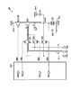
- FIG. 3 is a diagram showing an example of a pixel circuit configuration in a display device.
- FIG. 4 is a diagram showing an example of the cross-sectional structure of the display device according to the comparative example of the present embodiment.
- FIG. 5 is a diagram showing another example of the cross-sectional structure of the display device according to the comparative example of the present embodiment.
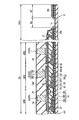
- FIG. 6 is a diagram showing an example of a cross-sectional structure of the display device according to the present embodiment.
- FIG. 7 is a plan view showing an example of the layout of the conductive layer with respect to the pixels in the present embodiment.
- FIG. 1 is a perspective view schematically showing a configuration of a display device according to an embodiment.
- FIG. 2 is a plan view showing a circuit configuration of the display device.
- FIG. 3 is a diagram showing
- FIG. 8 is a plan view showing an example of the layout of the conductive layer with respect to the pixel PX in the comparative example of the present embodiment.
- FIG. 9 is a plan view showing another example of the layout of the conductive layer with respect to the pixels in the present embodiment.
- FIG. 10 is a timing chart showing output examples of various signals related to the reset operation of the drive transistor, the offset cancel operation, the writing operation of the pixel signal, and the light emitting operation of the light emitting element in the display device according to the present embodiment.
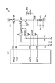
- FIG. 11 is a diagram for explaining an outline of the reset operation of the drive transistor.
- FIG. 12 is a diagram for explaining an outline of the offset cancel operation.
- FIG. 13 is a diagram for explaining an outline of the image signal writing operation.
- FIG. 14 is a diagram for explaining an outline of the image signal writing operation.
- FIG. 15 is a diagram for explaining an outline of the light emitting operation of the light emitting element.
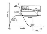
- FIG. 16 is a diagram for explaining the timing at which a current starts to flow in the light emitting element.
- FIG. 17 is a diagram for explaining the relationship between the output current of the drive transistor and the current flowing through the light emitting element.
- FIG. 18 is a diagram for explaining the relationship between the potential rise of the source electrode of the drive transistor and the current flowing through the light emitting element.
- FIG. 19 is a diagram showing an example of the cross-sectional structure of the display device when the common electrode is arranged on the same layer as the pixel electrode.
- FIG. 20 is a plan view showing an example of the layout of the conductive layer with respect to the pixels when the pixel electrodes and the common electrodes are arranged in the same layer.
- FIG. 1 is a perspective view schematically showing the configuration of the display device 1 according to the present embodiment.
- FIG. 1 shows a three-dimensional space defined by a first direction X, a second direction Y perpendicular to the first direction X, and a third direction Z perpendicular to the first direction X and the second direction Y. ..
- the first direction X and the second direction Y are orthogonal to each other, but may intersect at an angle other than 90 °.
- the third direction Z is defined as upper, and the direction opposite to the third direction Z is defined as lower.
- the second member may be in contact with the first member and is located away from the first member. You may be.
- the display device 1 is a micro LED display device (micro LED display) using a micro LED which is a self-luminous element will be described.
- the display device 1 includes a display panel 2, a first circuit board 3, a second circuit board 4, and the like.
- the display panel 2 has a rectangular shape in one example.
- the short side EX of the display panel 2 is parallel to the first direction X
- the long side EY of the display panel 2 is parallel to the second direction Y.
- the third direction Z corresponds to the thickness direction of the display panel 2.
- the main surface of the display panel 2 is parallel to the XY plane defined by the first direction X and the second direction Y.
- the display panel 2 has a display area DA and a non-display area NDA outside the display area DA.
- the non-display area NDA has a terminal area MT. In the illustrated example, the non-display area NDA surrounds the display area DA.
- the display area DA is an area for displaying an image, and includes, for example, a plurality of pixel PXs arranged in a matrix.
- the pixel PX includes a light emitting element (micro LED), a switching element (driving transistor) for driving the light emitting element, and the like.
- the terminal area MT is provided along the short side EX of the display panel 2 and includes a terminal for electrically connecting the display panel 2 to an external device or the like.
- the first circuit board 3 is mounted on the terminal area MT and is electrically connected to the display panel 2.
- the first circuit board 3 is, for example, a flexible printed circuit board.
- the first circuit board 3 includes a drive IC chip (hereinafter, referred to as a panel driver) 5 for driving the display panel 2.
- the panel driver 5 is arranged on the first circuit board 3, but may be arranged below the first circuit board 3. Further, the panel driver 5 may be mounted on a circuit board other than the first circuit board 3, for example, the panel driver 5 may be mounted on the second circuit board 4.
- the second circuit board 4 is, for example, a flexible printed circuit board.
- the second circuit board 4 is connected to the first circuit board 3 at, for example, below the first circuit board 3.
- the panel driver 5 described above is connected to a control board (not shown) via, for example, a second circuit board 4.
- the panel driver 5 executes control for displaying an image on the display panel 2 by driving a plurality of pixels PX based on, for example, a video signal output from the control board.
- the display panel 2 may have a bending region BA indicated by a diagonal line.
- the bent area BA is an area that is bent when the display device 1 is housed in a housing such as an electronic device.
- the bent region BA is located on the terminal region MT side of the non-display region NDA.
- the first circuit board 3 and the second circuit board 4 can be arranged below the display panel 2 so as to face the display panel 2 by bending the bending region BA.
- FIG. 2 is a plan view showing the circuit configuration of the display device 1.
- the display device 1 includes an active matrix type display panel 2.
- the display panel 2 has an insulating substrate 21.
- a plurality of pixels PX, various wirings, gate drivers GD1 and GD2, and a selection circuit SD are arranged on the insulating substrate 21.
- the plurality of pixels PX are arranged in a matrix in the display area DA.
- Each of the plurality of pixels PX has a plurality of sub-pixels.
- the pixel PX includes three types of sub-pixels: a sub-pixel SPR exhibiting a first color, a sub-pixel SPG exhibiting a second color, and a sub-pixel SPB exhibiting a third color.
- the first color, the second color, and the third color are, for example, red, green, and blue, respectively.
- the pixel PX includes a light emitting element (micro LED) and a pixel circuit for supplying a driving current to the light emitting element and driving the light emitting element.
- the pixel circuit includes a drive transistor and various switching elements described later.
- the various wirings described above extend in the display area DA and are drawn out to the non-display area NDA.
- a plurality of control wiring SSGs and a plurality of image signal lines VL are exemplified as a part of various wirings.
- control wiring SSG and the image signal line VL are connected to the sub-pixels SPR, SPG and SPB.
- the control wiring SSG is connected to the gate drivers GD1 and GD2 in the non-display area NDA.
- the image signal line VL is connected to the selection circuit SD in the non-display area NDA.
- the gate drivers GD1 and GD2 and the selection circuit SD are located in the non-display area NDA. Various signals and voltages are given to the gate drivers GD1 and GD2 and the selection circuit SD from the panel driver 5.
- the pixel PX has sub-pixels SPR, SPG and SPB, but the sub-pixels SPR, SPG and SPB are similarly configured. Therefore, for convenience, the configuration (pixel circuit) of one sub-pixel (hereinafter, referred to as sub-pixel SP) of the sub-pixel SPR, SPG, and SPB will be mainly described here.
- the sub-pixel SP includes a light emitting element LED, a drive transistor DRT, an output transistor BCT, a pixel transistor SST, an initialization transistor IST, a reset transistor RST, a holding capacity Cs, and an auxiliary capacity Cad. In this embodiment, these are arranged for each sub-pixel SP.
- Each transistor shown in FIG. 3 is an n-channel type transistor.
- the output transistor BCT, the pixel transistor SST, the initialization transistor IST, and the reset transistor RST do not have to be composed of transistors.
- the output transistor BCT, the pixel transistor SST, the initialization transistor IST, and the reset transistor RST may function as an output switch, a pixel switch, an initialization switch, and a reset switch, respectively.
- one of the source electrode and the drain electrode of the transistor will be the first electrode, and the other will be the second electrode. Further, one electrode of the capacitive element is used as a first electrode, and the other electrode is used as a second electrode.
- the drive transistor DRT, the pixel electrode described later, and the light emitting element LED are connected in series between the first power supply line PVH and the second power supply line PVL.
- the first power supply line PVH is held at a constant potential
- the second power supply line PVL is held at a constant potential different from the potential of the first power supply line PVH.
- the potential PVDD of the first power supply line PVH is higher than the potential PVSS of the second power supply line PVL.
- the potential P VDD of the first power supply line PVH is, for example, 9 V
- the potential PVSS of the second power supply line PVL is, for example, 0 V.
- the first electrode of the drive transistor DRT is connected to the first electrode (anode) of the light emitting element LED, the first electrode of the holding capacity Cs, and the first electrode of the auxiliary capacity CAD.
- the second electrode of the drive transistor DRT is connected to the first electrode of the output transistor BCT.
- the drive transistor DRT is configured to control the current (current value) supplied to the light emitting element LED.
- the second electrode of the output transistor BCT is connected to the first power supply line PVH. Further, the second electrode (cathode) of the light emitting element LED is connected to the second power supply line PVL.
- the first electrode of the pixel transistor SST is connected to the gate electrode of the drive transistor DRT, the first electrode of the initialization transistor IST, and the second electrode of the holding capacity Cs.
- the second electrode of the pixel transistor SST is connected to the image signal line VL.
- the second electrode of the initialization transistor IST is connected to the initialization power line BL.
- the holding capacitance Cs is electrically connected between the gate electrode of the drive transistor DRT and the first electrode (source electrode). Although details will be described later, in the present embodiment, the value of the holding capacity Cs (capacity size) is smaller than the value of the auxiliary capacity CAD (capacity size).
- the second electrode of the auxiliary capacity CAD is held at a constant potential.
- the second electrode of the auxiliary capacitance CAD is connected to, for example, the first power supply line PVH and is held at the same constant potential (P VDD) as the potential of the first power supply line PVH.
- the second electrode of the auxiliary capacitance Cad may be held at the same constant potential (PVSS) as the potential of the second power supply line PVL, or a power source different from the first power supply line PVH and the second power supply line PVL. It may be held at the same constant potential as the line (third power line).
- the third power supply line as the wiring held at a constant potential, the initialization power supply line BL or the reset power supply line RL can be mentioned.
- the first electrode of the reset transistor RST is connected to the first electrode of the drive transistor DRT.
- the second electrode of the reset transistor RST is connected to the reset power line RL.
- An image signal Vsig such as a video signal is supplied to the image signal line VL.
- the image signal Vsig is a signal written to a pixel (here, a sub-pixel SP), the minimum value of the image signal Vsig is, for example, 0V, and the maximum value of the image signal Vsig is, for example, 3V.
- the initialization potential Vini is supplied to the initialization power line BL.
- the initialization potential Vini is, for example, 1.2V.
- the reset power line RL is set to the reset power potential Vrst.
- the reset power supply potential Vrst is given a potential having a potential difference with respect to PVSS so that the light emitting element LED does not emit light, and is, for example, -2V.
- the gate electrode of the output transistor BCT is connected to the control wiring SBG.
- An output control signal BG is supplied to the control wiring SBG.
- the gate electrode of the pixel transistor SST is connected to the control wiring SSG.
- a pixel control signal SG is supplied to this control wiring SSG.
- the gate electrode of the initialization transistor IST is connected to the control wiring SIG.
- An initialization control signal IG is supplied to this control wiring SIG.
- the gate electrode of the reset transistor RST is connected to the control wiring SRG.
- a reset control signal RG is supplied to this control wiring SRG.
- the element capacitance Cled shown in FIG. 3 is the capacitance between the first electrode (anode) and the second electrode (cathode) of the light emitting element LED.
- all the above transistors are assumed to be Nch TFTs, but for example, all the transistors other than the drive transistor DRT may be Pch TFTs, or Nch TFTs and Pch TFTs may be mixed.
- the drive transistor DRT may be a Pch TFT. In that case, it is sufficient that the light emitting element LED is configured so that a current flows in the opposite direction to the present embodiment.
- the auxiliary capacitance CAD may be coupled to the electrode on the drive transistor DRT side of the electrodes of the light emitting element LED.
- the display device 1 since the display device 1 includes two gate drivers GD1 and GD2, it is possible to supply power to one pixel PX (sub-pixel SP) from the gate drivers GD1 and GD2 on both sides. It is possible.
- the two-sided power supply method is adopted for the above-mentioned control wiring SSG, and the one-sided power supply method is adopted for the other control wiring.
- the display device 1 does not have to include two gate drivers GD1 and GD2, and may include at least one gate driver.
- the circuit configuration described in FIG. 3 is an example, and the circuit configuration of the display device 1 may be another configuration as long as it includes the drive transistor DRT, the holding capacitance Cs, and the auxiliary capacitance CAD described above. ..
- a part of the circuit configuration described with reference to FIG. 3 may be omitted, or another configuration may be added.
- the current (micro LED current) flowing through the light emitting element LED when the light emitting element LED emits light is defined by the following equation (1). Will be done.
- Cox is the gate capacitance per unit area
- ⁇ is the carrier mobility
- W is the channel width of the drive transistor DRT
- L is the channel length of the drive transistor DRT.
- Vsig represents the above-mentioned image signal Vsig, and is a write voltage value written in the sub-pixel SP.
- Vini represents the above-mentioned initialization potential, and is a gate voltage value of the drive transistor DRT at the time of offset cancellation (Vth correction).
- Cs is the value of the above-mentioned holding capacity Cs
- Cad is the value of the above-mentioned auxiliary capacity (additional capacity) CAD
- Ced is the value of the above-mentioned element capacity Cled.
- the element capacity Cled is the capacity of the area of the light emitting element LED, and is proportional to the size of the light emitting element LED. Therefore, when the display device 1 is made high-definition, the size of the light emitting element LED is reduced, so that the value of the element capacitance Cled is smaller than the value of the holding capacitance Cs.
- the auxiliary capacitance CAD of the equation (1) is considerably smaller than the holding capacitance Cs, for example, the current required to make the light emitting element LED emit light is generated. It may not be possible to secure it. It is conceivable to increase the Vsig of the equation (1) in order to secure the required current, but since the output amplitude of the Vsig is limited to the output amplitude of the panel driver, it may not be possible to increase it freely. .. Therefore, it is important to secure a sufficient auxiliary capacity CAD.
- FIG. 4 is a diagram schematically showing an example of the cross-sectional structure of the display device according to the comparative example of the present embodiment.
- the display device includes the display panel 2', and one pixel PX (sub-pixel SPR, SPG) arranged in the display area DA of the display panel 2'is provided.
- SPB and the cross-sectional structure of the non-display area NDA will be mainly described.
- the non-display area NDA includes a bending area BA that can be bent and a terminal area MT.
- a glass substrate such as quartz or non-alkali glass, or a resin substrate such as polyimide can be mainly used.
- the resin substrate has flexibility, and a display device can be configured as a sheet display.
- the resin substrate is not limited to polyimide, and other resin materials may be used.
- the insulating substrate 21 may be referred to as an organic insulating layer, a resin layer, or the like.
- the undercoat layer 22 having a three-layer laminated structure is provided on the insulating substrate 21.
- the undercoat layer 22 is a first layer 22a formed of silicon oxide (SiO2), a second layer 22b formed of silicon nitride (SiN), and a third layer formed of silicon oxide (SiO2). It has 22c.
- the first layer 22a of the lowermost layer is provided as a blocking film of moisture and impurities from the outside in order to improve the adhesion to the insulating substrate 21 which is the base material.
- the third layer 22c of the uppermost layer is provided as a block film for preventing hydrogen atoms contained in the second layer 22b from diffusing toward the semiconductor layer SC side described later.
- the undercoat layer 22 is not limited to this structure.
- the undercoat layer 22 may be further laminated, or may have a single-layer structure or a two-layer structure.
- the silicon nitride film has relatively good adhesion, so that the silicon nitride film may be formed directly on the insulating substrate 21.
- the light-shielding layer 23 is arranged on the insulating substrate 21.
- the position of the light-shielding layer 23 is adjusted to the position where the TFT is formed later.
- the light-shielding layer 23 is made of, for example, metal, but may be made of a material having light-shielding properties such as a black layer.
- the light-shielding layer 23 is provided on the first layer 22a and is covered with the second layer 22b.
- the light-shielding layer 23 may be provided on the insulating substrate 21 and covered with the first layer 22a.
- a light-shielding layer 23 it is possible to suppress the intrusion of light into the back surface of the TFT channel, so that it is possible to suppress a change in TFT characteristics due to light that can be incident from the insulating substrate 21 side. .. Further, when the light-shielding layer 23 is formed of a conductive layer, it is possible to impart a back gate effect to the TFT by applying a predetermined potential to the light-shielding layer 23.
- a thin film transistor such as a drive transistor DRT is formed on the undercoat layer 22 described above.
- TFT Thin Film Transistor
- a polysilicon TFT that uses polysilicon for the semiconductor layer SC is taken as an example.
- the semiconductor layer SC is formed using low-temperature polysilicon.
- the drive transistor DRT is an N-channel type TFT (Nch TFT).
- the semiconductor layer SC of the Nch TFT has a channel region between a first region, a second region, a first region and a second region, a channel region and a first region, and a channel region and a second region, respectively. It has a low-concentration impurity region provided.
- One of the first and second regions functions as a source region, and the other of the first and second regions functions as a drain region.
- a silicon oxide film is used as the gate insulating film GI.
- the gate electrode GE is made of MoW (molybdenum / tungsten).
- the wiring and electrodes formed on the gate insulating film GI such as the gate electrode GE are referred to as 1st wiring or 1st metal.
- the gate electrode GE has a function as a holding capacitance electrode, which will be described later, in addition to a function as a gate electrode of the TFT.
- the top gate type TFT is described here as an example, the TFT may be a bottom gate type TFT.
- An interlayer insulating film 24 is provided on the gate insulating film GI and the gate electrode GE.
- the interlayer insulating film 24 is formed by laminating, for example, a silicon nitride film and a silicon oxide film in this order on the gate insulating film GI and the gate electrode GE.
- the gate insulating film GI and the interlayer insulating film 24 are not provided in the bent region BA.
- the gate insulating film GI and the interlayer insulating film 24 are patterned to correspond to the bent region BA.
- the part to be used is removed.
- the undercoat layer 22 is also patterned to remove the portion corresponding to the bent region BA.
- polyimide constituting the insulating substrate 21 is exposed. It should be noted that the etching of the undercoat layer 22 may cause a film loss in which the upper surface of the insulating substrate 21 is partially eroded.
- a wiring pattern (not shown) may be formed in the lower layers of the stepped portion at the end of the interlayer insulating film 24 and the stepped portion at the end of the undercoat layer 22. According to this, when the routing wiring LL formed in the next step crosses the stepped portion, it passes over the wiring pattern. Since there is a gate insulating film GI between the interlayer insulating film 24 and the undercoat layer 22, and there is, for example, a light-shielding layer 23 between the undercoat layer 22 and the insulating substrate 21, wiring is performed using these layers. A pattern can be formed.
- a first electrode E1, a second electrode E2, and a routing wiring LL are provided on the interlayer insulating film 24.
- a three-layer laminated structure (Ti system / Al system / Ti system) is adopted for each of the first electrode E1, the second electrode E2, and the routing wiring LL.
- the lower layer is made of a metal material containing Ti as a main component, such as Ti (titanium) and an alloy containing Ti.
- the intermediate layer is made of a metal material containing Al as a main component, such as Al (aluminum) and an alloy containing Al.
- the upper layer is made of a metal material containing Ti as a main component, such as Ti and an alloy containing Ti.
- the wiring and electrodes formed on the interlayer insulating film 24 such as the first electrode E1 are referred to as 2nd wiring or 2nd metal.
- the first electrode E1 is connected to the first region of the semiconductor layer SC.
- the second electrode E2 is connected to the second region of the semiconductor layer SC.
- the first electrode E1 is a source electrode and the second electrode E2 is a drain electrode.
- the first electrode E1 forms a holding capacitance Cs together with the interlayer insulating film 24 and the gate electrode (holding capacitance electrode) GE of the TFT.
- the routing wiring LL extends to the end of the peripheral edge of the insulating substrate 21 and forms a terminal for connecting the first circuit board 3 and the panel driver (drive IC) 5. Since the routing wiring LL is formed so as to cross the bending region BA and reach the terminal portion, it crosses the step of the interlayer insulating film 24 and the undercoat layer 22. Since the wiring pattern by the light-shielding layer 23 is formed in the stepped portion as described above, even if the routing wiring LL has a step break in the recess of the step, the continuity is maintained by contacting the lower wiring pattern. It is possible.
- the flattening film 25 is formed on the interlayer insulating film 24, the first electrode E1, the second electrode E2, and the routing wiring LL so as to cover the TFT and the routing wiring LL.
- an organic insulating material such as photosensitive acrylic is often used. Compared to the inorganic insulating material formed by CVD or the like, it is excellent in coverage of wiring steps and flatness of the surface.
- the flattening film 25 is removed at the pixel contact portion and the peripheral region.
- a conductive layer including the conductive layers 26a and 26b is provided on the flattening film 25.
- This conductive layer is formed of, for example, ITO (indium tin oxide) as the oxide conductive layer.
- the conductive layer 26a covers the portion where the first electrode E1 is exposed due to, for example, the removal of the flattening film 25.
- One of the purposes of the conductive layer 26a is to serve as a barrier film for preventing the exposed portion of the first electrode E1 and the routing wiring LL from being damaged in the manufacturing process.
- the wiring and electrodes formed on the flattening film 25 such as the conductive layer 26b are referred to as 3rd wiring or 3rd metal. Further, the conductive layer 26c shown in FIG. 4 may be formed as the conductive layer forming the surface of the terminal portion.
- the flattening film 25 and the conductive layers (conductive layers 26a and 26b) are covered with an insulating layer 27.
- the insulating layer 27 is formed of, for example, a silicon nitride film.
- a pixel electrode 28 is formed on the insulating layer 27.
- the pixel electrode 28 contacts the conductive layer 26a through the opening of the insulating layer 27 and is electrically connected to the first electrode E1.
- the pixel electrode 28 serves as a connection terminal for mounting a light emitting element LED (LED chip).
- the pixel electrode 28 is formed of a laminated body including a single conductive layer and two or more conductive layers. In the pixel electrode 28, for example, a two-layer laminated structure (Al system / Mo system) is adopted.
- the lower layer is made of Mo, a metal material containing Mo as a main component, such as an alloy containing Mo.
- the upper layer is made of a metal material containing Al as a main component, such as Al and an alloy containing Al.
- the conductive layer 26b, the insulating layer 27, and the pixel electrode 28 form the above-mentioned auxiliary capacitance CAD.
- An insulating layer 29 is provided on the insulating layer 27 and the pixel electrode 28.
- the insulating layer 29 is made of, for example, silicon nitride.
- the insulating layer 29 insulates the end portion of the pixel electrode 28 and the like, and has an opening for mounting the light emitting element LED on a part of the surface of the pixel electrode 28.
- the size of the opening of the insulating layer 29 is set to be one size larger than that of the light emitting element LED in consideration of the amount of mounting deviation in the mounting process of the light emitting element LED. For example, when the light emitting element LED has a mounting area of substantially 10 ⁇ m ⁇ 10 ⁇ m, it is preferable that the opening is substantially secured at 20 ⁇ m ⁇ 20 ⁇ m.
- the light emitting element LED is mounted on the array substrate AR (pixel electrode 28).
- the light emitting element LED has an anode AN, a cathode CA, and a light emitting layer LI that emits light.
- the anode AN and the cathode CA are arranged at positions facing each other via the light emitting layer LI.
- Light emitting element LEDs having emission colors of R, G, and B are prepared respectively, and the anode side terminal is in contact with and fixed to the corresponding pixel electrode 28.
- the light emitting element LED having a red emission color is LED (R)
- the light emitting element LED having a green emission color is LED (G)
- the light emitting element LED having a blue emission color is LED. It is shown as (B).
- the light emitting element LED (R) is a light emitting element LED included in the sub-pixel SPR
- the light emitting element LED (G) is a light emitting element LED included in the sub pixel SPG
- the light emitting element LED (B) is a sub. It is a light emitting element LED included in a pixel SPB.
- the bonding between the anode AN of the light emitting element LED and the pixel electrode 28 is not particularly limited as long as good continuity can be ensured between them and the formation of the array substrate AR is not damaged.
- a reflow process using a low-temperature molten solder material a method such as placing a light emitting element LED on an array substrate AR via a conductive paste and then bonding by firing, or a method of bonding the surface of the pixel electrode 28 and the anode of the light emitting element LED.
- a solid-layer bonding method such as ultrasonic bonding can be adopted by using a material similar to AN.
- the element insulating layer 30 is provided on the array substrate AR on which the light emitting element LED is mounted.
- the element insulating layer 30 is formed of a resin material filled in the gaps between the light emitting element LEDs on the array substrate AR.
- the element insulating layer 30 exposes the surface of the cathode CA of the light emitting element LEDs.
- the counter electrode 31 is arranged at a position facing the pixel electrode 28 via the light emitting element LED.
- the counter electrode 31 is formed on the surface of the cathode CA of the counter electrode 31 and on the element insulating layer 30, and is electrically connected to the cathode CA by coming into contact with the cathode CA.
- the counter electrode 31 needs to be formed as a transparent electrode in order to take out the emitted light from the light emitting element LED.
- the counter electrode 31 is formed by using, for example, ITO as the transparent conductive material.
- the counter electrode 31 commonly connects the cathode CAs of the plurality of light emitting element LEDs mounted in the display area DA. Although not shown, the counter electrode 31 is connected to, for example, a wiring provided on the AR side of the array substrate by a cathode contact portion provided outside the display area DA.
- the counter electrode 31 is formed so as to cover the display region DA in a plan view, extends to the non-display region NDA, and is electrically connected to the conductive layer 26d.
- the conductive layer 26d is connected to the second power supply line PVL.
- the side wall portion of the light emitting element LED is insulated with a protective film or the like, it is not always necessary to fill the gap with a resin material or the like, and the resin material is the anode AN and the pixel electrode 28 exposed from the anode AN. It suffices if it can at least insulate the surface.
- the element insulating layer 30 is formed with a film thickness that does not reach the cathode CA of the light emitting element LED, and subsequently the counter electrode 31 is formed. Although a part of the unevenness due to the mounting of the light emitting element LED remains on the surface on which the counter electrode 31 is formed, it is sufficient that the material forming the counter electrode 31 can be continuously covered without step breakage.
- the array substrate AR has a structure from the insulating substrate 21 to the counter electrode 31, but if necessary, a cover member such as a cover glass, a touch panel substrate, or the like is provided on the counter electrode 31. You may be.
- the cover member and the touch panel substrate may be provided, for example, via a filler using a resin or the like.
- auxiliary capacitance CAD is formed by the conductive layer 26b, the insulating layer 27, and the pixel electrode 28 as described in FIG. 4, but in order to secure a sufficient auxiliary capacitance CAD, it overlaps with the pixel electrode 28 in a plan view. It is preferable to increase the area of the conductive layer 26b (3rd metal).
- the conductive layer 26b is other than the contact portion that electrically connects, for example, the pixel electrode 28 and the first electrode E1 (drive transistor DRT) as shown in FIG. It is formed in the area of.
- the display device according to the comparative example of the present embodiment when the light emitting element LED (LED chip) is mounted on the array substrate AR (pixel electrode 28) as described above, the array substrate AR is damaged. Is easy to give, and point defects may occur.
- the conductive layer 26b connected to the DC power supply (first power supply line PVH) is arranged directly under the pixel electrode 28.
- the insulating layer 27 provided between the layer 26b and the pixel electrode 28 is thin, and there is a possibility that the pixel electrode 28 and the conductive layer 26b may be short-circuited by pressing the LED chip when the light emitting element LED is mounted.
- the display device 1 overlaps with the region of the pixel electrode 28 on which the light emitting element LED is mounted (hereinafter, referred to as the mounting region of the light emitting element LED) in a plan view. It is assumed that the conductive layer 26b is formed so as not to prevent it.
- FIG. 6 shows the cross-sectional structure of the display device 1 according to the present embodiment, but since it is the same as FIG. 4 except for the above-mentioned conductive layer 26b, detailed description thereof will be omitted here.
- the present embodiment may be applied to the cross-sectional structure shown in FIG.
- the conductive layer 26b shown in FIG. 5 may be formed so as not to overlap with the mounting region of the light emitting element LED in a plan view.
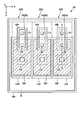
- FIG. 7 is a plan view showing an example of the layout (shape) of the conductive layer 26b with respect to the pixel PX (sub-pixel SPR, SPG and SPB) in the present embodiment.
- the pixel PX including the sub-pixels SPR, SPG, and SPB share a single conductive layer 26b.
- the conductive layer 26b is formed so as to extend continuously over the plurality of sub-pixels SPR, SPG and SPB (plurality of pixels PX).
- the conductive layer 26b is located below the pixel electrode 28 as described above.
- the pixel electrode 28 included in the sub-pixel SPR (that is, the pixel electrode 28 connected to the light emitting element LED (R) of the sub-pixel SPR) is designated as the pixel electrode 28R for convenience.
- the pixel electrode 28 included in the sub-pixel SPG (that is, the pixel electrode 28 connected to the light emitting element LED (G) of the sub-pixel SPG) is designated as the pixel electrode 28G for convenience.
- the pixel electrode 28 included in the sub-pixel SPB (that is, the pixel electrode 28 connected to the light emitting element LED (B) of the sub-pixel SPB) is designated as the pixel electrode 28B for convenience.
- the pixel electrode 28R is formed in a rectangular shape. Further, the pixel electrodes 28G and 28B are formed in a non-rectangular shape. The pixel electrodes 28R, 28G and 28B are formed so that the size of the pixel electrodes 28R is the largest and the sizes of the pixel electrodes 28G and 28B are the same. The sizes of the pixel electrodes 28G and 28B may be different.
- the arrangement areas LAR, LAG and LAB are arranged in the first direction X.
- the arrangement area LAR is an area in which the remaining elements other than, for example, the auxiliary capacitance CAD (pixel electrode 28R) of the pixel circuit of the sub-pixel SPR are arranged.
- the arrangement area LAG is an area in which the remaining elements other than, for example, the light emitting element LED (G) and the auxiliary capacitance CAD (pixel electrode 28G) are arranged in the pixel circuit of the sub-pixel SPG.
- the arrangement area LAB is an area in which the remaining elements other than, for example, the light emitting element LED (B) and the auxiliary capacitance CAD (pixel electrode 28B) are arranged in the pixel circuit of the sub-pixel SPB.
- the light emitting element LED (R) is located in the arrangement area LAR, but the light emitting element LEDs (G) and the LED (B) are located so as to straddle the arrangement areas LAG and LAB, respectively.
- the pixel electrode 28R is located in the arrangement region LAR and further located in the arrangement region LAG.
- each of the pixel electrodes 28G and 28B is located in the arrangement regions LAG and LAB.
- the pixel electrodes 28 (28R, 28G and 28B) may be provided so as to be located in the arrangement region of the adjacent pixel PX.
- the conductive layer 26b has openings 41R, 41G and 41B.
- the opening 41R is an opening formed in the conductive layer 26b for contacting the pixel electrode 28R and the first electrode E1 (drive transistor DRT) included in the sub-pixel SPR.
- the opening 41G is an opening formed in the conductive layer 26b for contacting the pixel electrode 28G and the first electrode E1 (drive transistor DRT) included in the sub-pixel SPG.
- the opening 41B is an opening formed in the conductive layer 26b for contacting the pixel electrode 28B and the first electrode E1 (drive transistor DRT) included in the sub-pixel SPB.
- the openings 41R, 41G and 41B that is, the contact portions for electrically connecting each of the pixel electrodes 28R, 28G and 28B and the drive transistor DRT
- the openings 41R, 41G and 41B extend in the first direction X. It is arranged in a straight line.
- the conductive layer 26b has openings 42R, 42G and 42B.
- the opening 42R is an opening formed in the conductive layer 26b so that the conductive layer 26b does not overlap with the mounting region of the light emitting element LED (R) of the sub-pixel SPR.
- the opening 42G is an opening formed in the conductive layer 26b so that the conductive layer 26b does not overlap with the mounting region of the light emitting element LED (G) of the sub-pixel SPG.
- the opening 42B is an opening formed in the conductive layer 26b so that the conductive layer 26b does not overlap with the mounting region of the light emitting element LED (B) of the sub-pixel SPB.
- the opening 42R is formed to be one size larger than the mounting region of the light emitting element LED (R) in a plan view.
- the opening 42R may be formed to have the same size as the opening provided in the insulating layer 29 described above (the opening for mounting the light emitting element LED (R)), for example.
- the opening 42R may be formed to be at least larger than the mounting area of the light emitting element LED (R). Further, in the opening 42R, the conductive layer 26b does not overlap with the mounting region of the light emitting element LED (R), and the end of the mounting region and the end of the conductive layer 26b (opening 42R) do not intersect. It suffices if it is formed in. Here, the opening 42R has been described, but the same applies to the openings 42G and 42B.
- At least one of the openings 42R, 42G and 42B is one straight line. It is formed so as not to be arranged in a shape. Specifically, the openings 42R and 42G are arranged in a straight line extending in the first direction X, but the openings 42B are not arranged in a straight line extending in the first direction X. Further, the openings 42G and 42B are arranged in a straight line extending in the second direction Y, but the openings 42R are not arranged in a straight line extending in the second direction Y.
- FIG. 8 shows an example of the layout (shape) of the conductive layer 26b with respect to the pixel PX (sub-pixel SPR, SPG and SPB) in the comparative example of the present embodiment.
- the conductive layer 26b directly under each mounting region of the light emitting elements LED (R), LED (G) and LED (B) is hollowed out.
- the openings 42R, 42G and 42B By forming the openings 42R, 42G and 42B in the space, it is possible to suppress a situation in which the pixel electrodes 28 (28R, 28G and 28B) and the conductive layer 26b are short-circuited when the light emitting element LED is mounted. it can.
- the sizes of the openings 42R, 42G, and 42B shown in FIG. 7 may be the same or different.
- the size of each of the openings 42R, 42G and 42G is, for example, the size of the light emitting elements LED (R), LED (G) and LED (B) (that is, the LED chip mounted on the pixel electrodes 28R, 28G and 28B). It may be decided based on.
- the value (magnitude) of the auxiliary capacitance CAD described above is proportional to the area of the conductive layer 26b that overlaps with the pixel electrode 28. Therefore, when the pixel electrode 28R is larger than the pixel electrodes 28G and 28B as shown in FIG. 7, the auxiliary capacitance CAD in each of the sub-pixel SPG and SPB is smaller than the auxiliary capacitance CAD in the sub-pixel SPR.
- the opening 42R so as to have a relatively large size, priority is given to suppressing the occurrence of the above-mentioned point defects (that is, a short circuit between the pixel electrode 28R and the conductive layer 26b), and the opening is opened.
- the portions 42G and 42B so as to be relatively smaller in size than the opening 42R, the occurrence of point defects may be minimized and the auxiliary capacity CAD may be secured as much as possible. That is, in the present embodiment, the sizes of the openings 42R, 42G and 42B may be determined according to the emission color of the light emitting element LED mounted on the pixel electrode 28 or the size of the pixel electrode 28. .. Further, in order to secure the auxiliary capacity CAD, the size of the pixel electrodes 28R, 28G and 28B may be increased according to the size of the openings 42R, 42G and 42B.
- FIG. 6 shows the cross-sectional structure of the display device 1 according to the present embodiment.
- the portion corresponding to the sub-pixel SPB shown in FIG. 6 has a cross-sectional structure along the line AA shown in FIG. (That is, the cross-sectional structure including the openings 41B and 42B) is shown.
- the layout of the conductive layer 26b shown in FIG. 7 described above is an example, and the conductive layer 26b may be formed as shown in FIG. 9, for example.
- the pixel electrodes 28R, 28G, and 28B are each formed in a rectangular shape, and are arranged side by side (striped) in the first direction X.
- the openings 41R, 41G and 41B are in the first direction X. It is arranged in an extending straight line.
- the openings 42R, 42G and 42B are arranged in a straight line extending in the first direction X. There is.
- the pixel electrodes 28R, 28G and 28B are arranged as shown in FIG. 9, the pixel electrodes 28 are formed by forming the openings 42R, 42G and 42B in the conductive layer 26b. It is possible to suppress a situation in which (28R, 28G and 28B) and the conductive layer 26b are short-circuited.
- At least the pixel electrodes 28G and 28B can be made larger than in the case shown in FIG. 7, for example, so that the auxiliary capacitance CAD in the sub-pixel SPG and SPB can be secured. ..
- the openings 42G and 42B can be formed with a sufficient size, it is possible to improve the reliability of suppressing the occurrence of defects at the time of mounting the light emitting element LED.
- the openings 42R, 42G and 42B are arranged in a straight line, but the openings 42R, 42G and 42B may be arranged so as to have a V shape, for example.
- the reset control signal RG is input to the first electrode (source electrode) of the drive transistor DRT so that the reset is performed without going through the drive transistor DRT. ing.
- the reset transistors are arranged for each pixel, not in the driver.
- the drive transistor DRT of each sub-pixel is used for signal writing (without mobility correction).
- the anodes will be connected, and signal color mixing may occur between R, G, and B. Therefore, in the present embodiment, the output transistor BCT is arranged for each sub-pixel.
- FIG. 10 is a timing chart showing output examples of various signals related to the reset operation, offset cancel (OC) operation, write operation, and light emission operation in the display device 1.
- signals supplied mainly to the control wirings SRG, SBG, SIG and SSG will be described.
- each of the above operations is performed in units of rows of pixel PX.
- the reset control signal supplied to the control wiring SRG connected to the pixel PX in the first row is supplied to RG1
- the output control signal supplied to the control wiring SBG is supplied to BG1
- the initial stage is supplied to the control wiring SIG.
- the conversion control signal is shown as IG1
- the pixel control signal supplied to the control wiring SSG is shown as SG1.
- the reset control signal supplied to the control wiring SRG connected to the pixel PX in the second row is supplied to the RG2, and the output control signal supplied to the control wiring SBG is supplied to the BG2 and the control wiring SIG.
- the initialization control signal is shown as IG2
- the pixel control signal supplied to the control wiring SSG is shown as SG2.
- control signals related to the pixel PX reset operation, offset cancel operation, image signal writing operation, and light emitting operation of the first line will be described. The details of each operation will be described later.
- the reset operation, offset cancel operation, write operation, and light emission operation in each pixel PX one of the pixels SPR, SPG, and SPB (RGB) is selected according to the signal (SELR / G / B) output from the panel driver 5. It is executed by doing.
- the output control signal BG1 changes from the H level to the L level
- the reset control signal RG1 changes from the L level to the H level.
- the current between the first power supply line PVH and the second power supply line PVL via the output transistor BCT is blocked, and the reset wiring (wiring connected to the first electrode of the reset transistor RST) is reset.
- the power supply potential Vrst resets between the output transistor BCT and the anode AN of the light emitting element LED.
- the initialization control signal IG1 changes from L level to H level.
- the initialization transistor IST is turned on, the initialization power line BL of the initialization potential Vini and the holding capacitance Cs are electrically connected, and the holding capacitance Cs is reset at the initial overpotential (Vini).
- the output control signal BG1 whose signal was at the L level prior to the reset of the holding capacity Cs becomes the H level when the reset period of the holding capacity Cs is completed. Further, the reset control signal RG1 becomes L level as the reset period of the holding capacity Cs is completed.
- the initialization control signal IG1 becomes L level when the offset cancellation period is completed.
- the pixel control signal SG1 changes from L level to H level.
- a current corresponding to the image signal Vsig flows through the pixel transistor SST to the holding capacitance Cs or the like via the image signal line VL, and an electric charge corresponding to the image signal Vsig is accumulated in the holding capacitance Cs.
- the writing operation to the pixel PX (pixel PSR, SPG and SPB) of the first line is completed.
- the light emitting element LED emits light when a current flows through the light emitting element LED according to the current value determined based on the above-mentioned image signal Vsig.
- control signals related to the reset operation, offset cancel operation, write operation, and light emission operation of the pixel PX in the first line have been described, but the same applies to each operation (control signal) in the pixel PX in the second and subsequent lines.
- the writing of the image signal Vsig is performed within 1H (horizontal scanning period of one line).
- the reset operation and the offset cancel operation shall be performed in parallel with the writing of the preceding pixel.
- the reset operation and the offset cancel operation are completed before the writing operation of the image signal Vsig, but the timing of writing the image signal Vsig is substantially the same as that of, for example, a liquid crystal display (LCD). Since the adjustment of the period in which the reset operation is performed and the period in which the offset cancel operation is performed is independent of the writing operation of the image signal Vsig, the degree of freedom is high.
- the first electrode of the drive transistor DRT connected to the first electrode of the holding capacity Cs described above is the source electrode
- the second electrode of the drive transistor DRT connected to the first electrode of the output transistor BCT. Is described as a drain electrode.
- the output control signal BG and the pixel control signal SG are set to the L level, and the initialization control signal IG and the reset control signal RG are set to the H level.
- the source potential of the drive transistor DRT is set to the reset power supply voltage Vrst (for example, -2V), and the gate potential of the drive transistor DRT is set to the initialization potential Vini (for example, 1.2V).
- Vrst for example, -2V
- Vini for example, 1.2V
- the drive transistor DRT is turned on, and the reset power supply voltage Vrst is charged to the source electrode of the drive transistor DRT.
- the current Iled flowing through the light emitting element LED by applying the reset power supply voltage Vrst is 0.
- the output control signal BG is switched from the L level to the H level, and the reset control signal RG is switched from the H level to the L level.
- the output transistor BCT is switched to the ON state, and the reset transistor RST is switched to the OFF state.
- the drive transistor DRT since the drive transistor DRT is in the ON state, the current supplied to the drain electrode of the drive transistor DRT flows through the channel of the drive transistor DRT, and the potential of the source electrode of the drive transistor DRT rises. After that, when the difference between the potential of the source electrode of the drive transistor DRT and the potential of the gate electrode reaches the threshold voltage (Vth) of the drive transistor DRT, the drive transistor DRT is turned off. In other words, the voltage between the gate electrode and the source electrode of the drive transistor DRT converges to a voltage substantially equal to the threshold value of the drive transistor DRT, and the potential difference corresponding to this threshold value is held in the holding capacitance Cs.
- Vth threshold voltage
- an initialization potential (Vini) is supplied to the gate electrode of the drive transistor DRT, and when the potential of the source electrode of the drive transistor DRT reaches Vini-Vth, the drive transistor DRT is turned off. As a result, an offset corresponding to the variation in Vth of the drive transistor DRT is generated between the gate electrode and the source electrode of the drive transistor DRT. As a result, the offset cancel operation of the threshold value of the drive transistor DRT is completed.
- the offset cancel operation is performed to maintain the threshold value (Vth) of the drive transistor DRT between the gate electrode and the source electrode of the drive transistor DRT.
- the output transistor BCT and the initialization transistor IST are turned off by switching the output control signal BG and the initialization control signal IG from the H level to the L level before the writing operation of the image signal Vsig. It can be switched to the state. As a result, the current path from the first power supply line PVH (P VDD) to the source electrode of the drive transistor DRT is cut off.
- the gate electrode of the drive transistor DRT holds Vini
- the source electrode of the drive transistor DRT holds Vini-Vth
- the voltage (Vgs) between the gate electrode and the source electrode of the drive transistor DRT is Vth (DRT).
- the pixel control signal SG is switched from the L level to the H level as shown in FIG.
- the pixel transistor SST can be switched to the ON state.
- the image signal Vsig is written to the gate electrode of the drive transistor DRT through the pixel transistor SST.
- the voltage value of the image signal Vsig is a value in the range of 0 to 3V.
- the dynamic range of the image signal Vsig is the same for the sub-pixels SPR, SPG, and SPB.
- the voltage Vgs of the drive transistor DRT is different even when the same image signal Vsig is written. ..
- the voltage Vgs is represented by the following equation (2).
- the output transistor BCT since the output transistor BCT is in the OFF state, the light emitting element LED does not light (light up).
- Vini is adjusted so as not to exceed the threshold value (Vth-LED) of the above-mentioned light emitting element LED even during the writing operation.
- the output control signal BG is switched from the L level to the H level, and the pixel control signal SG is switched from the H level to the L level. According to this, the output transistor BCT is switched to the ON state and the pixel transistor SST is switched to the OFF state.
- Vgs is constant. In this case, the potential of the gate electrode of the drive transistor DRT also starts to rise. This phenomenon is called bootstrap.
- the potential (DRT-S) of the source electrode (anode of the light emitting element LED) of the drive transistor DRT at the end of the writing operation is
- the display device 1 (display panel 2) according to the present embodiment can display various images by causing the light emitting element LEDs of each pixel PX (sub-pixel SPR, SPG, and SPB) to emit light by each of the above operations. ..
- the conductive layer 26b is provided between the pixel electrode 28 and the drive transistor DRT so as to overlap at least a part of the pixel electrode 28 in a plan view. 26b does not overlap with the region of the pixel electrode 28 (mounting region of the light emitting element LED) on which the light emitting element LED is mounted in a plan view.
- the pixel electrode 28 anode
- the conductive layer 26b 3rd metal
- the conductive layer 26b is formed over a plurality of pixels PX (sub-pixels SPR, SPG and SPB), and is formed at a position overlapping with the mounting region of the light emitting element LED in a plan view. With such a configuration, it is possible to avoid a short circuit between the pixel electrode 28 and the conductive layer 26b as described above.
- the conductive layer 26b has been described as having an opening, but the conductive layer 26b may be formed so as not to overlap with the mounting region of the light emitting element LED. That is, for example, a slit (gap region) or the like may be formed in the conductive layer 26b instead of the opening.
- the conductive layer 26b is formed so that the end portion of the conductive layer 26b and the end portion of the mounting region of the light emitting element LED do not intersect in a plan view, and the above-mentioned opening or slit may be formed. There are no restrictions on the shape or size of the.
- the shape of the pixel electrode 28, the arrangement of the contact portion for electrically connecting the pixel electrode 28 and the drive transistor DRT, the arrangement of the mounting area of the light emitting element LED, and the like are as shown in FIG. 7, for example. It may be, or it may be as shown in FIG.
- the opening 42R By providing 42G and 42B, it is possible to suppress the occurrence of defects.
- the counter electrode 31 is arranged at a position facing the pixel electrode 28 via the light emitting element LED, but it is connected to the anode of the light emitting element LED.
- the arrangement of the electrodes to be formed and the electrodes connected to the cathode of the light emitting element LED may be different from that in FIG.
- an electrode (hereinafter referred to as a common electrode) 32 connected to the cathode CA of the light emitting element LED is on the same layer as the pixel electrode 28 connected to the anode AN of the light emitting element LED. May be arranged.
- the conductive layer 26b arranged between the layer on which the pixel electrode 28 and the common electrode 32 are arranged and the drive transistor DRT is the mounting region of the light emitting element LED (the light emitting) in the plan view. It may be formed so as not to overlap with the area of the pixel electrode 28 and the common electrode 32 on which the element LED is mounted).
- FIG. 19 for convenience, only the cross-sectional structure relating to the sub-pixel SPB is shown, but the same applies to the other sub-pixel SPR and SPG.
- the gap between the pixel electrode 28 and the common electrode 32 and the gap between the anode AN and the cathode CA of the light emitting element LED shown in FIG. 19 are, for example, a resin material so as to be along the upper surfaces of the anode AN and the cathode CA of the light emitting element LED. Is flattened using.
- the common electrode 32 may be continuously formed so as to be in contact with the cathode CA of each light emitting element LED (IOT sputtering or the like).
- FIG. 20 shows the layout (shape) of the conductive layer 26b with respect to the pixel PX (sub-pixel SPR, SPG and SPB) when the pixel electrode 28 and the common electrode 32 are arranged in the same layer as shown in FIG. ) Is a plan view showing an example.
- FIG. 20 the same reference numerals are given to the same parts as those in FIG. 7 described above. Here, detailed description of the same parts as in FIG. 7 will be omitted, and parts different from FIG. 7 will be mainly described.
- the pixel PX including the sub-pixels SPR, SPG and SPB shares a single conductive layer 26b and also shares a single common electrode 32.
- the pixel electrode 28 and the common electrode 32 are arranged in the same layer. Therefore, in the plan view of FIG. 20, the pixel electrodes 28R, 28G, and 28B are formed in a rectangular shape, respectively, and are arranged in the openings formed in the common electrode 32.
- the light emitting element LED (R) is arranged so as to straddle the pixel electrode 28R and the common electrode 32. Specifically, in the light emitting element (R), the anode AN of the light emitting element LED (R) is connected to the pixel electrode 28R, and the anode CA of the light emitting element LED (R) is connected to the common electrode 32. Will be implemented. Although the light emitting element LED (R) has been described here, the same applies to the other light emitting element LEDs (G) and the LED (B).
- the conductive layer 26b has openings 41R, 41G and 41B.
- the opening 41R is an opening formed in the conductive layer 26b for contacting the pixel electrode 28R and the drive transistor DRT included in the sub-pixel SPR.
- the opening 41G is an opening formed in the conductive layer 26b for contacting the pixel electrode 28G and the drive transistor DRT included in the sub-pixel SPG.
- the opening 41B is an opening formed in the conductive layer 26b for contacting the pixel electrode 28B and the drive transistor DRT included in the sub-pixel SPB.
- the openings 41R, 41G and 41B are arranged in a straight line extending in the first direction X.
- the conductive layer 26b has openings 42R, 42G and 42B.
- the opening 42R is an opening formed in the conductive layer 26b so that the conductive layer 26b does not overlap with the mounting region of the light emitting element LED (R) of the sub-pixel SPR.
- the opening 42G is an opening formed in the conductive layer 26b so that the conductive layer 26b does not overlap with the mounting region of the light emitting element LED (G) of the sub-pixel SPG.
- the opening 42B is an opening formed in the conductive layer 26b so that the conductive layer 26b does not overlap with the mounting region of the light emitting element LED (B) of the sub-pixel SPB.
- the openings 42R, 42G and 42B are arranged in a straight line extending in the first direction X.
- the opening 42R is formed to be one size larger than the mounting region of the light emitting element LED (R) in a plan view.
- the opening 42R may be formed to have the same size as the opening provided in the insulating layer 29 (the opening for mounting the light emitting element LED (R)).
- the opening 42R may be formed to be at least larger than the mounting area of the light emitting element LED (R). Further, the opening 42R is formed so as not to overlap with the mounting region of the light emitting element LED (R) and so that the end of the mounting region and the end of the conductive layer 26b (opening 42R) do not intersect. Just do it.
- the opening 42R has been described, but the same applies to the openings 42G and 42B.
- the portion corresponding to the sub-pixel SPB shown in FIG. 19 above shows a cross-sectional structure along the line BB shown in FIG. 20 (that is, a cross-sectional structure including openings 41B and 42B).
- FIG. 20 an example is shown in which the openings 41R, 41G and 41B and the openings 42R, 42G and 42B are arranged in a straight line extending in the first direction X, respectively.
- the arrangement of the portions (that is, the arrangement of the contact portion between the pixel electrode 28 and the drive transistor DRT or the mounting area of the light emitting element LED) may be different from that shown in FIG.
- this embodiment is applicable even when the pixel electrodes 28 and the common electrodes 32 are arranged in the same layer (that is, when the electrodes of the micro LED have the same layer structure), and the defects are The occurrence can be suppressed.
Landscapes
- Engineering & Computer Science (AREA)
- Physics & Mathematics (AREA)
- Computer Hardware Design (AREA)
- General Physics & Mathematics (AREA)
- Theoretical Computer Science (AREA)
- Devices For Indicating Variable Information By Combining Individual Elements (AREA)
- Control Of El Displays (AREA)
- Led Device Packages (AREA)
- Control Of Indicators Other Than Cathode Ray Tubes (AREA)
Abstract
実施形態に係る表示装置は、基板と、基板上に配置された画素電極と、画素電極上に実装された発光素子と、画素電極を介して発光素子に対して供給される電流を制御する駆動トランジスタと、画素電極と駆動トランジスタとの間に、平面視において当該画素電極と少なくとも一部が重畳するように形成された導電層とを具備する。導電層は、平面視において発光素子が実装されている画素電極の領域と重畳しない。
Description
本発明の実施形態は、表示装置に関する。
自発光素子である発光ダイオード(LED:Light Emitting Diode)を用いたLEDディスプレイが知られているが、近年では、より高精細化した表示装置として、マイクロLEDと称される微小な発光ダイオード素子を用いた表示装置(以下、マイクロLEDディスプレイと表記)が開発されている。
このマイクロLEDディスプレイは、従来の液晶表示ディスプレイや有機ELディスプレイと異なり、表示領域に、チップ状の多数のマイクロLED(以下、LEDチップと表記)が実装されて形成されるため、高精細化と大型化の両立が容易であり、次世代ディスプレイとして注目されている。
ところで、マイクロLEDディスプレイの製造時には上記したLEDチップがアレイ基板に実装されるが、この際にアレイ基板にダメージを与えやすく、マイクロLEDディスプレイにおける欠陥の発生の要因となる。
そこで、本発明が解決しようとする課題は、欠陥の発生を抑制することが可能な信頼性の高い表示装置を提供することにある。
実施形態に係る表示装置は、基板と、前記基板上に配置された画素電極と、前記画素電極上に実装された発光素子と、前記画素電極を介して前記発光素子に対して供給される電流を制御する駆動トランジスタと、前記画素電極と前記駆動トランジスタとの間に、平面視において当該画素電極と少なくとも一部が重畳するように形成された導電層とを具備する。前記導電層は、平面視において前記発光素子が実装されている前記画素電極の領域と重畳しない。
以下、図面を参照して、実施形態について説明する。なお、開示はあくまで一例に過ぎず、当業者において、発明の趣旨を保っての適宜変更について容易に想到し得るものについては、当然に本発明の範囲に含有されるものである。また、図面は、説明をより明確にするため、実際の態様に比べて、各部の幅、厚さ、形状等について模式的に表される場合があるが、あくまで一例であって、本発明の解釈を限定するものではない。また、本明細書と各図において、既出の図に関して前述したものと同一または類似した機能を発揮する構成要素には同一の参照符号を付し、重複する詳細な説明を適宜省略することがある。
図1は、本実施形態に係る表示装置1の構成を概略的に示す斜視図である。図1は、第1方向Xと、第1方向Xに垂直な第2方向Yと、第1方向X及び第2方向Yに垂直な第3方向Zによって規定される三次元空間を示している。なお、第1方向X及び第2方向Yは、互いに直交しているが、90°以外の角度で交差していてもよい。また、本実施形態においては、第3方向Zを上と定義し、第3方向Zと反対側の方向を下と定義する。「第1部材の上の第2部材」及び「第1部材の下の第2部材」とした場合、第2部材は、第1部材に接していてもよく、第1部材から離れて位置していてもよい。
以下、本実施形態においては、表示装置1が自発光素子であるマイクロLEDを用いたマイクロLED表示装置(マイクロLEDディスプレイ)である場合について説明する。
図1に示すように、表示装置1は、表示パネル2、第1回路基板3及び第2回路基板4等を備える。
表示パネル2は、一例では矩形状である。図示した例では、表示パネル2の短辺EXは、第1方向Xと平行であり、表示パネル2の長辺EYは、第2方向Yと平行である。第3方向Zは、表示パネル2の厚さ方向に相当する。表示パネル2の主面は、第1方向Xと第2方向Yとにより規定されるX-Y平面に平行である。表示パネル2は、表示領域DA、及び表示領域DAの外側の非表示領域NDAを有している。非表示領域NDAは、端子領域MTを有している。図示した例では、非表示領域NDAは、表示領域DAを囲んでいる。
表示領域DAは、画像を表示する領域であり、例えばマトリクス状に配置された複数の画素PXを備えている。画素PXは、発光素子(マイクロLED)及び当該発光素子を駆動するためのスイッチング素子(駆動トランジスタ)等を含む。
端子領域MTは、表示パネル2の短辺EXに沿って設けられ、表示パネル2を外部装置等と電気的に接続するための端子を含んでいる。
第1回路基板3は、端子領域MTの上に実装され、表示パネル2と電気的に接続されている。第1回路基板3は、例えばフレキシブルプリント回路基板である。第1回路基板3は、表示パネル2を駆動する駆動ICチップ(以下、パネルドライバと表記)5等を備えている。なお、図示した例において、パネルドライバ5は、第1回路基板3の上に配置されているが、第1回路基板3の下に配置されていてもよい。また、パネルドライバ5は、第1回路基板3以外に実装されていてもよく、例えば第2回路基板4に実装されていてもよい。
第2回路基板4は、例えばフレキシブルプリント回路基板である。第2回路基板4は、第1回路基板3の例えば下方において第1回路基板3と接続されている。
上記したパネルドライバ5は、例えば第2回路基板4を介して制御基板(図示せず)と接続されている。パネルドライバ5は、例えば制御基板から出力される映像信号に基づいて複数の画素PXを駆動することによって表示パネル2に画像を表示する制御を実行する。
なお、表示パネル2は、斜線を付して示す折り曲げ領域BAを有していてもよい。折り曲げ領域BAは、表示装置1が電子機器等の筐体に収容される際に折り曲げられる領域である。折り曲げ領域BAは、非表示領域NDAのうち端子領域MT側に位置している。第1回路基板3及び第2回路基板4は、折り曲げ領域BAが折り曲げられることによって、表示パネル2と対向するように、表示パネル2の下方に配置されることができる。
図2は、表示装置1の回路構成を示す平面図である。図2に示すように、表示装置1は、アクティブマトリクス型の表示パネル2を備えている。表示パネル2は、絶縁基板21を有する。この絶縁基板21上には、複数の画素PXと、各種配線と、ゲートドライバGD1及びGD2と、選択回路SDとが配置されている。
複数の画素PXは、表示領域DAにおいてマトリクス状に配列されている。複数の画素PXの各々は、複数の副画素を有している。本実施形態において、画素PXは、第1色を呈する副画素SPR、第2色を呈する副画素SPG及び第3色を呈する副画素SPBの3種類の副画素を含む。ここでは、第1色、第2色及び第3色は、例えばそれぞれ赤色、緑色及び青色であるものとする。
画素PXは、発光素子(マイクロLED)と、発光素子に駆動電流を供給し、当該発光素子を駆動するための画素回路とを含む。画素回路は、後述する駆動トランジスタ及び各種のスイッチング素子等を含む。
上記した各種配線は、表示領域DAにおいて延在し、非表示領域NDAに引き出されている。図2においては、各種配線の一部として、複数本の制御配線SSGと、複数本の画像信号線VLとが例示されている。
表示領域DAにおいて、制御配線SSG及び画像信号線VLは、副画素SPR、SPG及びSPBに接続されている。制御配線SSGは、非表示領域NDAにおいてゲートドライバGD1及びGD2に接続されている。画像信号線VLは、非表示領域NDAにおいて選択回路SDに接続されている。
ゲートドライバGD1及びGD2と選択回路SDとは、非表示領域NDAに位置している。ゲートドライバGD1、GD2及び選択回路SDには、パネルドライバ5から各種の信号や電圧が与えられる。
次に、図3を参照して、表示装置1における画素の回路構成(画素回路)の一例について説明する。本実施形態において、複数の画素PXは同様に構成されている。また、上記したように画素PXは副画素SPR、SPG及びSPBを有するが、当該副画素SPR、SPG及びSPBは同様に構成されている。このため、ここでは便宜的に、副画素SPR、SPG及びSPBのうちの1つの副画素(以下、副画素SPと表記)の構成(画素回路)について主に説明する。
図3に示すように、副画素SPは、発光素子LED、駆動トランジスタDRT、出力トランジスタBCT、画素トランジスタSST、初期化トランジスタIST、リセットトランジスタRST、保持容量Cs及び補助容量Cadを含む。本実施形態において、これらは副画素SP毎に配置される。
図3に示す各トランジスタは、nチャネル型トランジスタである。なお、出力トランジスタBCT、画素トランジスタSST、初期化トランジスタIST及びリセットトランジスタRSTは、それぞれトランジスタで構成されていなくてもよい。出力トランジスタBCT、画素トランジスタSST、初期化トランジスタIST及びリセットトランジスタRSTは、それぞれ、出力スイッチ、画素スイッチ、初期化スイッチ、リセットスイッチとして機能するものであればよい。
以下の説明においては、トランジスタのソース電極及びドレイン電極の一方を第1電極、他方を第2電極とする。また、容量素子の一方の電極を第1電極、他方の電極を第2電極とする。
駆動トランジスタDRT、後述する画素電極及び発光素子LEDは、第1電源線PVHと第2電源線PVLとの間で直列に接続されている。第1電源線PVHは定電位に保持され、第2電源線PVLは第1電源線PVHの電位とは異なる定電位に保持されている。本実施形態において、第1電源線PVHの電位PVDDは、第2電源線PVLの電位PVSSより高い。具体的には、第1電源線PVHの電位PVDDは例えば9Vであり、第2電源線PVLの電位PVSSは例えば0Vである。
駆動トランジスタDRTの第1電極は、発光素子LEDの第1電極(陽極)、保持容量Csの第1電極及び補助容量Cadの第1電極に接続されている。駆動トランジスタDRTの第2電極は、出力トランジスタBCTの第1電極に接続されている。駆動トランジスタDRTは、発光素子LEDに対して供給される電流(電流値)を制御するように構成されている。
出力トランジスタBCTの第2電極は、第1電源線PVHに接続されている。また発光素子LEDの第2電極(陰極)は、第2電源線PVLに接続されている。
画素トランジスタSSTの第1電極は、駆動トランジスタDRTのゲート電極、初期化トランジスタISTの第1電極及び保持容量Csの第2電極に接続されている。画素トランジスタSSTの第2電極は、画像信号線VLに接続されている。初期化トランジスタISTの第2電極は初期化電源線BLに接続されている。
保持容量Csは、駆動トランジスタDRTのゲート電極と第1電極(ソース電極)との間に電気的に接続されている。詳細については後述するが、本実施形態において、保持容量Csの値(容量サイズ)は、補助容量Cadの値(容量サイズ)より小さい。
補助容量Cadの第2電極は、定電位に保持されている。本実施形態において、補助容量Cadの第2電極は、例えば第1電源線PVHに接続され、第1電源線PVHの電位と同一の定電位(PVDD)に保持されている。なお、補助容量Cadの第2電極は、第2電源線PVLの電位と同一の定電位(PVSS)に保持されていてもよいし、第1電源線PVH及び第2電源線PVLとは異なる電源線(第3電源線)と同一の定電位に保持されていてもよい。第3電源線としては、定電位に保持される配線として、初期化電源線BLまたはリセット電源線RLを挙げることができる。
リセットトランジスタRSTの第1電極は、駆動トランジスタDRTの第1電極に接続されている。リセットトランジスタRSTの第2電極は、リセット電源線RLに接続されている。
画像信号線VLには、映像信号等の画像信号Vsigが供給される。画像信号Vsigは画素(ここでは、副画素SP)に書き込まれる信号であり、当該画像信号Vsigの最小値は例えば0Vであり、当該画像信号Vsigの最大値は例えば3Vである。
初期化電源線BLには、初期化電位Viniが供給される。初期化電位Viniは、例えば1.2Vである。
リセット電源線RLは、リセット電源電位Vrstに設定される。リセット電源電位Vrstは、PVSSに対して発光素子LEDが発光しないような電位差を有する電位が与えられ、例えば-2Vである。
出力トランジスタBCTのゲート電極は、制御配線SBGに接続されている。この制御配線SBGには、出力制御信号BGが供給される。
画素トランジスタSSTのゲート電極は、制御配線SSGに接続されている。この制御配線SSGには、画素制御信号SGが供給される。
初期化トランジスタISTのゲート電極は、制御配線SIGに接続されている。この制御配線SIGには、初期化制御信号IGが供給される。
リセットトランジスタRSTのゲート電極は、制御配線SRGに接続されている。この制御配線SRGには、リセット制御信号RGが供給される。
なお、図3に示す素子容量Cledは、発光素子LEDの第1電極(陽極)と第2電極(陰極)との間の容量である。
図3においては、上記の全てのトランジスタがNchTFTであるものとして説明したが、例えば駆動トランジスタDRT以外のトランジスタは、全てがPchTFTであってもよいし、NchTFT及びPchTFTが混在していてもよい。
また、駆動トランジスタDRTがPchTFTであってもよい。その場合、本実施形態とは逆向きに、発光素子LEDに電流が流れるように構成されていればよい。いずれの場合においても、補助容量Cadは、発光素子LEDの電極のうち駆動トランジスタDRT側の電極に結合されていればよい。
また、図2において説明したように、表示装置1は、2つのゲートドライバGD1及びGD2を備えているため、1つの画素PX(副画素SP)に両側のゲートドライバGD1及びGD2から給電することが可能である。ここでは、上記した制御配線SSGについては両側給電方式が採用されており、他の制御配線については片側給電方式が採用されているものとする。ただし、表示装置1は、2つのゲートドライバGD1及びGD2を備えていなくてもよく、少なくとも1つのゲートドライバを備えていればよい。
なお、図3において説明した回路構成は一例であり、上記した駆動トランジスタDRT、保持容量Cs及び補助容量Cadを含むものであれば、表示装置1の回路構成は他の構成であっても構わない。例えば図3において説明した回路構成のうちの一部が省略されていてもよいし、他の構成が追加されても構わない。
ここで、詳しい動作については後述するが、上記した図3に示す回路構成において発光素子LEDが発光する際に当該発光素子LEDに流れる電流(マイクロLED電流)は、以下の式(1)により定義される。

ここで、素子容量Cledは、発光素子LEDの面積が持つ容量であり、発光素子LEDのサイズに比例する。このため、表示装置1を高精細化した場合には、発光素子LEDのサイズが縮小するので、素子容量Cledの値は保持容量Csの値と比較して小さくなる。
素子容量Cledと保持容量Csとが上記した関係にある場合において、式(1)の補助容量Cadが例えば保持容量Csよりも相当小さいものとすると、発光素子LEDを発光させるために必要な電流を確保することができない場合がある。なお、必要な電流を確保するために式(1)のVsigを大きくすることが考えられるが、当該Vsigの出力振幅は、パネルドライバの出力振幅に制限されるので、自由に大きくできない場合がある。このため、補助容量Cadを十分に確保することが重要である。
以下、図4を参照して、本実施形態の比較例について説明する。図4は、本実施形態の比較例に係る表示装置の断面構造の一例を模式的に示す図である。
図4においては、本実施形態の比較例に係る表示装置が表示パネル2´を備えるものとし、当該表示パネル2´が有する表示領域DAに配置されている1つの画素PX(副画素SPR、SPG及びSPB)及び非表示領域NDAの断面構造について主に説明する。なお、非表示領域NDAは、折り曲げられる折り曲げ領域BAと、端子領域MTとを含んでいる。
図4に示すように、表示パネル2´のアレイ基板ARは、絶縁基板21を備えている。絶縁基板21としては、主に、石英、無アルカリガラス等のガラス基板、またはポリイミド等の樹脂基板を用いることができる。樹脂基板は可撓性を有し、シートディスプレイとして表示装置を構成することができる。なお、樹脂基板としては、ポリイミドに限らず、他の樹脂材料を用いてもよい。これにより、絶縁基板21は、有機絶縁層または樹脂層等と称してもよい。
絶縁基板21上には、三層積層構造のアンダーコート層22が設けられている。アンダーコート層22は、シリコン酸化物(SiO2)で形成された第1層22a、シリコン窒化物(SiN)で形成された第2層22b、及びシリコン酸化物(SiO2)で形成された第3層22cを有している。最下層の第1層22aは基材である絶縁基板21との密着性向上のため、中層の第2層22bは外部からの水分及び不純物のブロック膜として設けられている。また、最上層の第3層22cは、第2層22b中に含有する水素原子が後述する半導体層SC側に拡散しないようにするブロック膜として設けられている。
なお、アンダーコート層22は、この構造に限定されるものではない。アンダーコート層22は、更に積層があってもよいし、単層構造または二層構造であってもよい。例えば、絶縁基板21がガラスである場合、シリコン窒化膜は比較的密着性がよいため、当該絶縁基板21上に直接シリコン窒化膜を形成しても構わない。
遮光層23は、絶縁基板21の上に配置されている。遮光層23の位置は、後にTFTを形成する箇所に合わせられている。本実施形態において、遮光層23は、例えば金属で形成されているが、黒色層等の遮光性を有する材料で形成されていればよい。
また、本実施形態において、遮光層23は、第1層22aの上に設けられ、第2層22bで覆われている。なお、遮光層23は、絶縁基板21の上に設けられ、第1層22aで覆われていてもよい。
このような遮光層23によれば、TFTチャネル裏面への光の侵入を抑制することができるため、絶縁基板21側から入射され得る光に起因したTFT特性の変化を抑制することが可能である。また、遮光層23を導電層で形成した場合には、当該遮光層23に所定の電位を与えることで、TFTにバックゲート効果を付与することも可能である。
上記したアンダーコート層22上には、駆動トランジスタDRT等の薄膜トランジスタ(TFT:Thin Film Transistor)が形成される。TFTとしては半導体層SCにポリシリコンを利用するポリシリコンTFTを例としている。本実施形態においては、低温ポリシリコンを利用して半導体層SCが形成されている。ここでは、駆動トランジスタDRTは、Nチャネル型のTFT(NchTFT)である。
NchTFTの半導体層SCは、第1領域と、第2領域と、第1領域及び第2領域の間のチャネル領域と、チャネル領域及び第1領域の間並びにチャネル領域及び第2領域の間にそれぞれ設けられた低濃度不純物領域とを有する。第1及び第2領域の一方がソース領域として機能し、第1及び第2領域の他方がドレイン領域として機能している。
ゲート絶縁膜GIとしては、シリコン酸化膜が用いられる。ゲート電極GEは、MoW(モリブデン・タングステン)で形成されている。なお、ゲート電極GE等のゲート絶縁膜GIの上に形成される配線や電極は、1st配線または1stメタルと称される。ゲート電極GEは、TFTのゲート電極としての機能に加え、後述する保持容量電極としての機能を有している。ここではトップゲート型のTFTを例として説明しているが、TFTはボトムゲート型のTFTであってもよい。
ゲート絶縁膜GI及びゲート電極GEの上には、層間絶縁膜24が設けられている。層間絶縁膜24は、ゲート絶縁膜GI及びゲート電極GEの上に、例えばシリコン窒化膜及びシリコン酸化膜を順に積層して構成されている。
なお、ゲート絶縁膜GI及び層間絶縁膜24は、折り曲げ領域BAに設けられていない。この場合、折り曲げ領域BAを含む絶縁基板21上の全領域に、ゲート絶縁膜GI及び層間絶縁膜24を形成した後、ゲート絶縁膜GI及び層間絶縁膜24にパターニングを行って折り曲げ領域BAに相当する箇所を除去している。更に、層間絶縁膜24等の除去によってアンダーコート層22が露出するため、当該アンダーコート層22についてもパターニングを行って折り曲げ領域BAに相当する箇所を除去している。アンダーコート層22を除去した後には、絶縁基板21を構成する例えばポリイミドが露出する。なお、アンダーコート層22のエッチングを通じて、絶縁基板21の上面が一部浸食された膜減りを生ずる場合がある。
この場合、層間絶縁膜24の端部における段差部分及びアンダーコート層22の端部における段差部分のそれぞれの下層に図示しない配線パターンを形成しておいてもよい。これによれば、次の工程で形成する引き回し配線LLが段差部分を横切る際に、配線パターンの上を通る。層間絶縁膜24とアンダーコート層22との間にはゲート絶縁膜GIがあり、アンダーコート層22と絶縁基板21との間には例えば遮光層23があるので、それらの層を利用して配線パターンを形成することができる。
層間絶縁膜24の上には、第1電極E1、第2電極E2及び引き回し配線LLが設けられている。第1電極E1、第2電極E2及び引き回し配線LLにおいては、それぞれ三層積層構造(Ti系/Al系/Ti系)が採用される。この三層積層構造において、下層は、Ti(チタン)、Tiを含む合金等のTiを主成分とする金属材料からなる。中間層は、Al(アルミニウム)、Alを含む合金等のAlを主成分とする金属材料からなる。上層は、Ti、Tiを含む合金等のTiを主成分とする金属材料からなる。なお、第1電極E1等の層間絶縁膜24の上に形成される配線や電極は、2nd配線または2ndメタルと称される。
第1電極E1は、半導体層SCの第1領域に接続されている。第2電極E2は、半導体層SCの第2領域に接続されている。例えば、半導体層SCの第1領域がソース領域として機能する場合、第1電極E1はソース電極であり、第2電極E2はドレイン電極である。この場合、第1電極E1は、層間絶縁膜24及びTFTのゲート電極(保持容量電極)GEとともに保持容量Csを形成する。
引き回し配線LLは、絶縁基板21の周縁の端部まで延在され、第1回路基板3やパネルドライバ(駆動IC)5を接続する端子を形成する。なお、引き回し配線LLは、折り曲げ領域BAを横切って端子部に到達するように形成されるため、層間絶縁膜24及びアンダーコート層22の段差を横切る。上記したように段差部分には遮光層23による配線パターンが形成されているため、引き回し配線LLが段差の凹部で段切れを生じたとしても、下の配線パターンにコンタクトすることで導通を維持することが可能である。
平坦化膜25は、TFT及び引き回し配線LLを覆うように、層間絶縁膜24、第1電極E1、第2電極E2及び引き回し配線LLの上に形成されている。平坦化膜25としては、感光性アクリル等の有機絶縁材料が多く用いられる。CVD等により形成される無機絶縁材料に比べ、配線段差のカバレッジ性や表面の平坦性に優れる。平坦化膜25は、画素コンタクト部及び周辺領域では除去される。
平坦化膜25の上には、導電層26a及び26bを含む導電層が設けられている。この導電層は、酸化物導電層として、例えばITO(インジウム・ティン・オキサイド)で形成されている。
導電層26aは、例えば平坦化膜25の除去により第1電極E1が露出した箇所を被覆する。導電層26aは、製造工程で第1電極E1や引き回し配線LLの露出部がダメージを負わないようにするためのバリア膜となることを目的の一つとしている。
なお、導電層26b等の平坦化膜25上に形成される配線や電極は、3rd配線または3rdメタルと称される。また、端子部の表面を形成する導電層として、図4に示す導電層26cが形成されていてもよい。
平坦化膜25及び導電層(導電層26a及び26b)は、絶縁層27で被覆されている。絶縁層27は、例えばシリコン窒化膜で形成されている。絶縁層27の上に、画素電極28が形成されている。画素電極28は、絶縁層27の開口を介して導電層26aにコンタクトし、第1電極E1に電気的に接続されている。ここでは、画素電極28は、発光素子LED(LEDチップ)を実装するための接続端子となる。画素電極28は、単一の導電層、二層以上の導電層を含む積層体で形成されている。画素電極28においては、例えば二層積層構造(Al系/Mo系)が採用される。この二層積層構造において、下層は、Mo、Moを含む合金等のMoを主成分とする金属材料からなる。上層は、Al、Alを含む合金等のAlを主成分とする金属材料からなる。
図4に示すように、導電層26b、絶縁層27及び画素電極28は、上記した補助容量Cadを形成している。
絶縁層27及び画素電極28の上には、絶縁層29が設けられている。絶縁層29は、例えばシリコン窒化物で形成されている。絶縁層29は、画素電極28の端部等を絶縁するとともに、画素電極28の表面の一部に発光素子LEDを実装するための開口を有している。絶縁層29の開口の大きさは、発光素子LEDの実装工程における実装ずれ量等を考慮し、発光素子LEDよりも一回り大きめの開口とする。例えば発光素子LEDが実質的に10μm×10μmの実装面積である場合、上記開口は実質的に20μm×20μmは確保されることが好ましい。
表示領域DAにおいては、アレイ基板AR(画素電極28)の上に、発光素子LEDが実装される。発光素子LEDは、陽極ANと、陰極CAと、光を放出する発光層LIとを有している。陽極AN及び陰極CAは、発光層LIを介して対向する位置に配置されている。
発光素子LEDは、R、G、Bの発光色を有するものがそれぞれ用意されており、対応する画素電極28に陽極側端子が接触し固定されている。図4に示す例おいては、赤色の発光色を有する発光素子LEDをLED(R)、緑色の発光色を有する発光素子LEDをLED(G)及び青色の発光色を有する発光素子LEDをLED(B)として示している。換言すれば、発光素子LED(R)は副画素SPRに含まれる発光素子LEDであり、発光素子LED(G)は副画素SPGに含まれる発光素子LEDであり、発光素子LED(B)は副画素SPBに含まれる発光素子LEDである。
発光素子LEDの陽極ANと画素電極28との間の接合は、両者の間で良好な導通が確保でき、かつ、アレイ基板ARの形成物を破損しないものであれば特に限定されない。例えば低温溶融のはんだ材料を用いたリフロー工程や、導電ペーストを介して発光素子LEDをアレイ基板AR上に載せた後に焼成結合する等の手法、或いは画素電極28の表面と、発光素子LEDの陽極ANとに同系材料を用い、超音波接合等の固層接合の手法を採用することができる。
発光素子LEDが実装されたアレイ基板ARの上には、素子絶縁層30が設けられている。素子絶縁層30は、アレイ基板ARの上で、発光素子LEDの間の空隙部に充填された樹脂材料で形成されている。なお、素子絶縁層30は、発光素子LEDのうち陰極CAの表面を露出させる。
対向電極31は、発光素子LEDを介して画素電極28と対向する位置に配置される。対向電極31は、対向電極31の陰極CAの表面と素子絶縁層30の上に形成され、陰極CAに接触することによって、当該陰極CAと電気的に接続される。対向電極31は、発光素子LEDからの出射光を取り出すために、透明電極として形成される必要がある。対向電極31は、透明導電材料として例えばITOを用いて形成される。対向電極31は、表示領域DAに実装された複数の発光素子LEDの陰極CAを共通に接続する。図示されていないが、対向電極31は、例えば表示領域DAの外側に設けられた陰極コンタクト部でアレイ基板AR側に設けられた配線と接続される。
対向電極31は、表示領域DAを平面視で覆うように形成されると共に、非表示領域NDAまで延在して、導電層26dと電気的に接続される。導電層26dは、第2電源線PVLに通じている。
一方、発光素子LEDの側壁部分が保護膜等で絶縁されている場合は、必ずしも樹脂材料等で間隙を充填する必要はなく、樹脂材料は、陽極ANと、陽極ANから露出した画素電極28の表面とを少なくとも絶縁することができればよい。この場合、図5に示すように発光素子LEDの陰極CAまで達しないような膜厚で素子絶縁層30を形成し、続けて上記対向電極31を形成する。対向電極31が形成される表面に発光素子LEDの実装に伴う凹凸の一部が残存しているが、対向電極31を形成する材料が段切れすることなく連続的に覆うことができればよい。
上記したようにアレイ基板ARは、絶縁基板21から対向電極31までの構造を有しているが、必要に応じて、対向電極31の上にカバーガラス等のカバー部材やタッチパネル基板等が設けられていてもよい。このカバー部材やタッチパネル基板は、例えば樹脂等を用いた充填剤を介して設けられてもよい。
図4を参照して本実施形態の比較例に係る表示装置(表示パネル2´)について説明したが、当該表示装置においては、上記したように十分な補助容量Cadを確保する必要がある。この補助容量Cadは図4において説明したように導電層26b、絶縁層27及び画素電極28によって形成されるが、十分な補助容量Cadを確保するためには、平面視において画素電極28と重畳する導電層26b(3rdメタル)の面積を大きくすることが好ましい。このため、本実施形態の比較例に係る表示装置において、導電層26bは、図4に示すように例えば画素電極28と第1電極E1(駆動トランジスタDRT)とを電気的に接続するコンタクト部以外の領域に形成されている。
しかしながら、本実施形態の比較例に係る表示装置の構成では、上記したように発光素子LED(LEDチップ)がアレイ基板AR(画素電極28)上に実装される際に、当該アレイ基板ARにダメージを与えやすく、点欠陥が発生する可能性がある。具体的には、本実施形態の比較例に係る表示装置においては、DC電源(第1電源線PVH)と接続されている導電層26bが画素電極28の直下に配置されているが、当該導電層26bと画素電極28との間に設けられている絶縁層27は薄く、発光素子LEDの実装時に、LEDチップの押圧によって画素電極28と導電層26bとがショートする可能性がある。
そこで、本実施形態に係る表示装置1においては、図6に示すように、平面視において発光素子LEDが実装されている画素電極28の領域(以下、発光素子LEDの実装領域と表記)と重畳しないように導電層26bが形成されているものとする。
なお、図6は本実施形態に係る表示装置1の断面構造を示しているが、上記した導電層26b以外は図4と同様であるため、ここではその詳しい説明を省略する。
また、本実施形態は、図5に示す断面構造に適用されても構わない。この場合、図5に示す導電層26bが、平面視において発光素子LEDの実装領域と重畳しないように形成されればよい。
ここで、図7は、本実施形態における画素PX(副画素SPR、SPG及びSPB)に対する導電層26bのレイアウト(形状)の一例を示す平面図である。
図7に示すように、副画素SPR、SPG及びSPBを含む画素PXは、単個の導電層26bを共用している。換言すれば、導電層26bは、複数の副画素SPR、SPG及びSPB(複数の画素PX)に亘って連続的に延在するように形成されている。なお、導電層26bは、上記したように画素電極28の下方に位置している。
また、図7においては、副画素SPRに含まれる画素電極28(つまり、副画素SPRの発光素子LED(R)に接続される画素電極28)を便宜的に画素電極28Rとする。更に、副画素SPGに含まれる画素電極28(つまり、副画素SPGの発光素子LED(G)に接続される画素電極28)を便宜的に画素電極28Gとする。同様に、副画素SPBに含まれる画素電極28(つまり、副画素SPBの発光素子LED(B)に接続される画素電極28)を便宜的に画素電極28Bとする。
図7の平面視において、画素電極28Rは、矩形状に形成されている。また、画素電極28G及び28Bは、非矩形状に形成されている。なお、画素電極28R、28G及び28Bは、画素電極28Rのサイズが最も大きく、画素電極28G及び28Bのサイズが同一となるように形成されている。なお、画素電極28G及び28Bのサイズは、異なっていてもよい。
また、配置領域LAR、LAG及びLABは、第1方向Xに並んでいる。ここで、配置領域LARは、副画素SPRの画素回路のうち例えば補助容量Cad(画素電極28R)以外の残りの素子が配置される領域である。配置領域LAGは、副画素SPGの画素回路のうち例えば発光素子LED(G)及び補助容量Cad(画素電極28G)以外の残りの素子が配置される領域である。配置領域LABは、副画素SPBの画素回路のうち例えば発光素子LED(B)及び補助容量Cad(画素電極28B)以外の残りの素子が配置される領域である。
なお、図7に示す例において、発光素子LED(R)は配置領域LARに位置しているが、発光素子LED(G)及びLED(B)はそれぞれ配置領域LAG及びLABに跨るように位置している。また、画素電極28Rは、配置領域LARに位置するとともに、配置領域LAGに更に位置している。また、画素電極28G及び28Bの各々は、配置領域LAG及びLABに位置している。なお、画素電極28(28R、28G及び28B)は、隣の画素PXの配置領域に位置するように設けられても構わない。
また、図7に示すように、導電層26bは、開口部41R、41G及び41Bを有する。開口部41Rは、画素電極28Rと副画素SPRに含まれる第1電極E1(駆動トランジスタDRT)とをコンタクトするために導電層26bに形成されている開口部である。開口部41Gは、画素電極28Gと副画素SPGに含まれる第1電極E1(駆動トランジスタDRT)とをコンタクトするために導電層26bに形成されている開口部である。開口部41Bは、画素電極28Bと副画素SPBに含まれる第1電極E1(駆動トランジスタDRT)とをコンタクトするために導電層26bに形成されている開口部である。図7に示す例において、開口部41R、41G及び41B(つまり、画素電極28R、28G及び28Bの各々と駆動トランジスタDRTとをそれぞれ電気的に接続するコンタクト部)は、第1方向Xに延在する直線状に配置されている。
更に、導電層26bは、開口部42R、42G及び42Bを有する。開口部42Rは、導電層26bが副画素SPRの発光素子LED(R)の実装領域と重畳しないように当該導電層26bに形成されている開口部である。開口部42Gは、導電層26bが副画素SPGの発光素子LED(G)の実装領域と重畳しないように当該導電層26bに形成されている開口部である。開口部42Bは、導電層26bが副画素SPBの発光素子LED(B)の実装領域と重畳しないように当該導電層26bに形成されている開口部である。
図7に示す例において、開口部42Rは、平面視において発光素子LED(R)の実装領域よりも一回り大きく形成されている。開口部42Rは、例えば上記した絶縁層29に設けられている開口(発光素子LED(R)を実装するための開口)と同程度の大きさに形成されていてもよい。
なお、開口部42Rは、少なくとも発光素子LED(R)の実装領域よりも大きく形成されていればよい。また、開口部42Rは、導電層26bが発光素子LED(R)の実装領域と重畳せず、かつ、当該実装領域の端部と導電層26b(開口部42R)の端部とが交差しないように形成されていればよい。ここでは、開口部42Rについて説明したが、開口部42G及び42Bについても同様である。
また、図7に示す例において、開口部42R、42G及び42B(つまり、発光素子LED(R)、LED(G)及びLED(B)の実装領域)のうちの少なくとも1つは、1つの直線状に配置されないように形成されている。具体的には、開口部42R及び42Gは第1方向Xに延在する直線状に配置されているが、開口部42Bは当該第1方向Xに延在する直線状には配置されていない。また、開口部42G及び42Bは第2方向Yに延在する直線状に配置されているが、開口部42Rは当該第2方向Yに延在する直線状には配置されていない。
ここで、図8は本実施形態の比較例における画素PX(副画素SPR、SPG及びSPB)に対する導電層26bのレイアウト(形状)の一例を示している。本実施形態においては、図8に示す本実施形態の比較例と比較して、発光素子LED(R)、LED(G)及びLED(B)の各々の実装領域直下の導電層26bをくり抜くように開口部42R、42G及び42Bが形成されていることによって、発光素子LEDの実装時に画素電極28(28R、28G及び28B)と導電層26bとがショートしてしまうような事態を抑制することができる。
なお、図7に示す開口部42R、42G及び42Bの各々のサイズは、同一であってもよいし、異なっていてもよい。開口部42R、42G及び42Gの各々のサイズは、例えば発光素子LED(R)、LED(G)及びLED(B)(つまり、画素電極28R、28G及び28B上に実装されるLEDチップ)のサイズに基づいて決定されればよい。
ここで、上記した補助容量Cadの値(大きさ)は、画素電極28と重畳する導電層26bの面積に比例する。そのため、図7に示すように画素電極28G及び28Bよりも画素電極28Rが大きい場合には、副画素SPG及びSPBの各々における補助容量Cadは副画素SPRにおける補助容量Cadよりも小さくなる。
このため、例えば開口部42Rについては比較的サイズが大きくなるように形成することによって上記した点欠陥の発生(つまり、画素電極28R及び導電層26b間のショート)を抑制することを優先し、開口部42G及び42Bについては開口部42Rよりも比較的サイズが小さくなるように形成することによって、点欠陥の発生を最低限抑制するとともに、補助容量Cadについても最大限確保するようにしてもよい。すなわち、本実施形態においては、画素電極28上に実装される発光素子LEDの発光色または当該画素電極28のサイズ等に応じて、開口部42R、42G及び42Bのサイズが決定されていてもよい。また、補助容量Cadを確保するために、開口部42R、42G及び42Bの大きさに応じて画素電極28R、28G及び28Bのサイズを大きくするように設計されてもよい。
なお、図6においては本実施形態に係る表示装置1の断面構造を示しているが、例えば図6に示す副画素SPBに対応する部分は、図7に示すA-A線に沿った断面構造(つまり、開口部41B及び42Bを含む断面構造)を示している。図7においては示されていないが、副画素SPR及びSPGについても同様である。
また、上記した図7に示す導電層26bのレイアウトは一例であり、導電層26bは、例えば図9に示すように形成されていてもよい。図9に示す例では、画素電極28R、28G及び28Bは、それぞれ矩形状に形成されており、第1方向Xに並んで(ストライプ状に)配置されている。
また、図9の平面視において、開口部41R、41G及び41B(つまり、画素電極28R、28G及び28Bの各々と駆動トランジスタDRTとをそれぞれ電気的に接続するコンタクト部)は、第1方向Xに延在する直線状に配置されている。
更に、開口部42R、42G及び42B(つまり、発光素子LED(R)、LED(G)及びLED(B)の各々の実装領域)は、第1方向Xに延在する直線状に配置されている。
本実施形態においては、図9に示すように画素電極28R、28G及び28Bが配置されている場合であっても、導電層26bに開口部42R、42G及び42Bを形成することによって、画素電極28(28R、28G及び28B)と導電層26bとがショートしてしまうような事態を抑制することができる。
なお、図9に示す構成によれば、例えば図7に示す場合と比較して少なくとも画素電極28G及び28Bを大きくすることができるため、副画素SPG及びSPBにおける補助容量Cadを確保することができる。この場合、余裕のあるサイズで開口部42G及び42Bを形成することができるため、発光素子LEDの実装時における欠陥の発生を抑制する信頼性を向上させることができる。
また、図9においては例えば開口部42R、42G及び42Bが直線状に配置されているが、当該開口部42R、42G及び42Bは、例えばV字形状となるように配置されていてもよい。
以下、表示装置1(図3に示す画素回路)における動作について説明する。なお、上記した図3に示す回路構成においては、リセット制御信号RGが駆動トランジスタDRTの第1電極(ソース電極)に入力される構成により、リセットが駆動トランジスタDRTを介さずに行うように構成されている。また、アノード間ショートの発生を回避するために、リセットトランジスタは、ドライバ内ではなく、画素毎に配置されている。更に、例えば出力トランジスタBCTを3つの副画素SPR、SPG及びSPBに対して1つ配置する構成の場合には、信号書き込み(移動度補正なし)の際に各副画素の駆動トランジスタDRTを介してアノード間が接続されることになり、R、G及びB間で信号混色が生じる場合がある。このため、本実施形態において、出力トランジスタBCTは、副画素毎に配置されている。
図10は、表示装置1におけるリセット動作、オフセットキャンセル(OC)動作、書き込み動作及び発光動作に関する各種信号の出力例を示すタイミングチャートである。ここでは、主に制御配線SRG、SBG、SIG及びSSGに供給される信号について説明する。
なお、上記した各動作は、画素PXの行単位で行われるものとする。図10においては、1行目の画素PXに接続されている制御配線SRGに供給されるリセット制御信号をRG1、制御配線SBGに供給される出力制御信号をBG1、制御配線SIGに供給される初期化制御信号をIG1、制御配線SSGに供給される画素制御信号をSG1として示している。
また、図10においては、2行目の画素PXに接続されている制御配線SRGに供給されるリセット制御信号をRG2、制御配線SBGに供給される出力制御信号をBG2、制御配線SIGに供給される初期化制御信号をIG2、制御配線SSGに供給される画素制御信号をSG2として示している。
詳しい説明は省略するが、図10に示す3行目及び4行目の画素PXに接続されている各制御配線に供給される制御信号についても同様である。図10においては、1行目~4行目の画素PXに対する各制御信号のタイミングを示しているが、5行目以降の画素PXについても同様である。
以下、1行目の画素PXのリセット動作、オフセットキャンセル動作、画像信号の書き込み動作及び発光動作に係る制御信号について説明する。なお、各動作の詳細については後述する。各画素PXにおけるリセット動作、オフセットキャンセル動作、書き込み動作及び発光動作は、パネルドライバ5から出力される信号(SELR/G/B)に従って画素SPR、SPG及びSPB(RGB)のうちの1つを選択することにより実行される。
また、表示装置1の回路構成においては全てのトランジスタがNchTFTである場合を想定しており、このようなトランジスタのゲート電極にロー(L)レベルの信号が供給されると当該トランジスタはOFF状態(非導通状態)となる。一方、このようなトランジスタのゲート電極にハイ(H)レベルの信号が供給されると当該トランジスタはON状態(導通状態)となる。
まず、保持容量Csのリセット動作に先立って、出力制御信号BG1がHレベルからLレベルになるとともに、リセット制御信号RG1がLレベルからHレベルになる。これにより、出力トランジスタBCTを介した第1電源線PVHと第2電源線PVLとの間での電流が遮られるとともに、リセット配線(リセットトランジスタRSTの第1電極に接続されている配線)のリセット電源電位Vrstで出力トランジスタBCTと発光素子LEDの陽極ANとの間がリセットされる。
次に、初期化制御信号IG1がLレベルからHレベルになる。この場合、初期化トランジスタISTがON状態となり、初期化電位Viniの初期化電源線BLと保持容量Csとが導通し、初期過電位(Vini)で保持容量Csがリセットされる。
なお、保持容量Csのリセットに先立って信号がLレベルになっていた出力制御信号BG1は、保持容量Csのリセット期間の完了に伴いHレベルになる。また、リセット制御信号RG1は、保持容量Csのリセット期間の完了に伴いLレベルになる。
また、初期化制御信号IG1は、オフセットキャンセル期間の完了に伴いLレベルになる。
その後、画素制御信号SG1がLレベルからHレベルになる。この場合、画像信号線VLを介して画像信号Vsigに応じた電流が画素トランジスタSSTを通じて保持容量Cs等に流れ、当該保持容量Csには画像信号Vsigに応じた電荷が蓄積される。これにより、1行目の画素PX(画素PSR、SPG及びSPB)への書き込み動作が完了する。
書き込み動作が完了した場合、上記した画像信号Vsigに基づいて決定される電流値に従って発光素子LEDに電流が流れることにより、当該発光素子LEDが発光する。
ここでは、1行目の画素PXのリセット動作、オフセットキャンセル動作、書き込み動作及び発光動作に関する制御信号について説明したが、2行目以降の画素PXにおける各動作(制御信号)についても同様である。
なお、画像信号Vsigの書き込みは、1H(1行の水平走査期間)内に実施されるものとする。また、リセット動作及びオフセットキャンセル動作は、前段画素の書き込みと並行して実施されるものとする。更に、リセット動作及びオフセットキャンセル動作は画像信号Vsigの書き込み動作の前に終了するが、画像信号Vsigの書き込みのタイミングは例えば液晶表示装置(LCD)と概ね同様である。なお、リセット動作が行われる期間及びオフセットキャンセル動作が行われる期間の調整は、画像信号Vsigの書き込み動作と独立しているため、自由度が高い。
以下、図11~16を参照して、表示装置1の動作の概要について説明する。なお、以下の説明においては、上記した保持容量Csの第1電極と接続される駆動トランジスタDRTの第1電極がソース電極、出力トランジスタBCTの第1電極と接続される駆動トランジスタDRTの第2電極がドレイン電極であるものとして説明する。
まず、図11を参照して、駆動トランジスタDRTのリセット動作の概要について説明する。
図11に示すように、駆動トランジスタDRTのリセット動作の場合、出力制御信号BG及び画素制御信号SGをLレベルとし、初期化制御信号IG及びリセット制御信号RGをHレベルとする。
これによれば、出力トランジスタBCTはOFF状態(BCT=OFF)、画素トランジスタSSTはOFF状態(SST=OFF)、初期化トランジスタISTはON状態(IST=ON)、リセットトランジスタRSTはON状態(RST=ON)となる。すなわち、この場合には、初期化トランジスタIST及びリセットトランジスタRSTがON状態に切り替えられている。
このような駆動トランジスタDRTのリセット動作においては、駆動トランジスタDRTのソース電位をリセット電源電圧Vrst(例えば、-2V)、駆動トランジスタDRTのゲート電位を初期化電位Vini(例えば、1.2V)とすることによって、駆動トランジスタDRTをON状態にして、リセット電源電圧Vrstを駆動トランジスタDRTのソース電極に充電する。なお、リセット電源電圧Vrstの印加によって発光素子LEDに流れる電流Iledは0である。
これにより、前フレームの情報がリセットされ、オフセットキャンセル動作の準備が完了する。
次に、図12を参照して、オフセットキャンセル動作の概要について説明する。図9に示すように、オフセットキャンセル動作の場合には、出力制御信号BGをLレベルからHレベルに切り替え、リセット制御信号RGをHレベルからLレベルに切り替える。これによれば、出力トランジスタBCTはON状態に、リセットトランジスタRSTはOFF状態に、それぞれ切り替えられる。
この場合、駆動トランジスタDRTのドレイン電極には、出力トランジスタBCTを介して第1電源線PVHから電流が流れ込む。
ここで、駆動トランジスタDRTはON状態となっているため、駆動トランジスタDRTのドレイン電極に供給された電流は駆動トランジスタDRTのチャネルを流れ、当該駆動トランジスタDRTのソース電極の電位が上昇する。その後、駆動トランジスタDRTのソース電極の電位とゲート電極の電位との差が駆動トランジスタDRTのしきい値電圧(Vth)に達すると、駆動トランジスタDRTはOFF状態となる。換言すれば、駆動トランジスタDRTのゲート電極-ソース電極間の電圧は駆動トランジスタDRTのしきい値と概ね等しい電圧に収束し、このしきい値に相当する電位差が保持容量Csに保持される。
具体的には、駆動トランジスタDRTのゲート電極には初期化電位(Vini)が供給されており、当該駆動トランジスタDRTのソース電極の電位がVini-Vthに達すると駆動トランジスタDRTはOFF状態となる。これにより、駆動トランジスタDRTのVthのばらつき分のオフセットが当該駆動トランジスタDRTのゲート電極-ソース電極間に生じる。これにより、駆動トランジスタDRTのしきい値のオフセットキャンセル動作は完了する。
上記したようにオフセットキャンセル動作は、駆動トランジスタDRTのゲート電極-ソース電極間に当該駆動トランジスタDRTのしきい値(Vth)を保持させるために行われる。
なお、第2電源線PVLの電位PVSSが0Vの場合、発光素子LEDの陽極と陰極との間(駆動トランジスタDRTのソース電極と第2電源線PVLとの間)の電位Vled=Vini-Vthとなる。この場合、Vledが発光素子LEDのしきい値(Vth-LED)を超えないようにVini(初期化電位)は調整されているものとする。
次に、図13及び図14を参照して、画像信号(映像信号)Vsigの書き込み動作の概要について説明する。
図13に示すように、画像信号Vsigの書き込み動作の前には、出力制御信号BG及び初期化制御信号IGをHレベルからLレベルに切り替えることによって、出力トランジスタBCT及び初期化トランジスタISTはそれぞれOFF状態に切り替えられる。これにより、第1電源線PVH(PVDD)から駆動トランジスタDRTのソース電極への電流経路を遮断しておく。
なお、この場合における駆動トランジスタDRTのゲート電極はViniを保持しており、当該駆動トランジスタDRTのソース電極はVini-Vthを保持している。これによれば、駆動トランジスタDRTのゲート電極-ソース電極間の電圧(Vgs)はVth(DRT)である。
画像信号Vsigの書き込み動作の場合には、図14に示すように、画素制御信号SGをLレベルからHレベルに切り替える。
これによれば、画素トランジスタSSTはON状態に切り替えられる。この場合、画素トランジスタSSTを通じて画像信号Vsigが駆動トランジスタDRTのゲート電極に書き込まれる。例えば、画像信号Vsigの電圧値は、0~3Vの範囲内の値である。そして、本実施形態において、画像信号Vsigのダイナミックレンジは、副画素SPR、SPG及びSPBで同一である。
ここで、駆動トランジスタDRTのソース電極は上記したオフセットキャンセル動作によりVthの値毎に異なる電位となっているため、同じ画像信号Vsigを書き込む場合であっても、当該駆動トランジスタDRTの電圧Vgsは異なる。画像信号Vsigの書き込みが完了した駆動トランジスタDRTにおいて、電圧Vgsは次の式(2)で表される。

また、書き込み動作時においても、上記した発光素子LEDのしきい値(Vth-LED)を超えないようにViniは調整されている。
次に、図15を参照して、発光素子LEDを発光させる発光動作の概要について説明する。発光動作の場合、出力制御信号BGをLレベルからHレベルに切り替え、画素制御信号SGをHレベルからLレベルに切り替える。これによれば、出力トランジスタBCTはON状態、画素トランジスタSSTはOFF状態に、それぞれ切り替えられる。
これにより、第1電源線PVH(PVDD)から駆動トランジスタDRTに電流が流れ始め、駆動トランジスタDRTのソース電極の電位が上昇を始める。
ここで、駆動トランジスタDRTのゲート電極はフローティングであるため、Vgsは一定となる。この場合、駆動トランジスタDRTのゲート電極の電位も合わせて上昇を開始する。なお、この現象はブートストラップと称される。
発光動作においては、図16に示すように、駆動トランジスタDRTのソース電極及びPVSS間の電圧(Vled)がVth-LED以上になると、発光素子LEDに電流Iledが流れ始める。この電流Iledにより、発光素子LEDは、点灯(発光)する。
なお、図17に示すように、発光動作(発光期間)における電流Iledは、駆動トランジスタDRTから与えられる出力電流(駆動トランジスタDRTの飽和領域の出力電流)Idrtに相当する(Iled=Idrt)。
ここで、書き込み動作終了時の駆動トランジスタDRTのソース電極(発光素子LEDのアノード)の電位(DRT-S)は、

この場合、図18に示すように、式(3)によって表される駆動トランジスタDRTのソース電極の電位が上昇し、発光素子LEDに電流が流れ始めた後、Idrt=Iledとなったところで、当該駆動トランジスタDRTのソース電極の電位上昇が止まり、定常状態となる。詳細については省略するが、この電流Iled(Idrt)は上記した式(1)によって表されるため、発光素子LEDにはVthに依存しない電流が流れることになる。
本実施形態に係る表示装置1(表示パネル2)は、上記した各動作によって各画素PX(副画素SPR、SPG及びSPB)の発光素子LEDを発光させることによって、各種画像を表示することができる。
上記したように本実施形態においては、画素電極28と駆動トランジスタDRTとの間に、平面視において当該画素電極28と少なくとも一部が重畳するように形成された導電層26bを備え、当該導電層26bは、平面視において発光素子LEDが実装されている画素電極28の領域(発光素子LEDの実装領域)と重畳しない。
本実施形態においては、このような構成により、発光素子LED(LEDチップ)を実装する際に画素電極28(アノード)と導電層26b(3rdメタル)とがショートし、例えば点欠陥のような欠陥が発生してしまうことを抑制することが可能となり、信頼性の高い表示装置を提供することができる。
なお、本実施形態において、導電層26bは、複数の画素PX(副画素SPR、SPG及びSPB)に亘って形成されており、平面視において発光素子LEDの実装領域(と重畳する位置に形成された開口部を有する。このような構成によれば、上記したように画素電極28と導電層26bとのショートを回避することができる。
本実施形態においては、導電層26bが開口部を有するものとして説明したが、当該導電層26bは発光素子LEDの実装領域と重畳しないように形成されていればよい。すなわち、導電層26bには、開口部の代わりに、例えばスリット(隙間領域)等が形成されていても構わない。
また、本実施形態においては、導電層26bの端部と発光素子LEDの実装領域の端部とが平面視において交差しないように導電層26bが形成されていればよく、上記した開口部またはスリットの形状または大きさについては制限されない。
なお、本実施形態において、画素電極28の形状、当該画素電極28と駆動トランジスタDRTとを電気的に接続するコンタクト部の配置、発光素子LEDの実装領域の配置等は、例えば図7に示すようであってもよいし、図9に示すようであってもよい。
すなわち、本実施形態においては、表示装置1が図7に示されるように構成されている場合であっても、図9に示されるように構成されている場合であっても、開口部42R、42G及び42Bを設けることによって、欠陥の発生を抑制することが可能となる。
なお、本実施形態においては、上記した図6に示すように発光素子LEDを介して画素電極28と対向する位置に対向電極31が配置される場合について説明したが、発光素子LEDの陽極に接続される電極及び当該発光素子LEDの陰極に接続される電極の配置は図6とは異なっていてもよい。
具体的には、図19に示すように、発光素子LEDの陽極ANに接続される画素電極28と同じ層に当該発光素子LEDの陰極CAに接続される電極(以下、共通電極と表記)32が配置されていてもよい。このような構成の場合には、画素電極28及び共通電極32が配置されている層と駆動トランジスタDRTとの間に配置された導電層26bが、平面視において発光素子LEDの実装領域(当該発光素子LEDが実装されている画素電極28及び共通電極32の領域)と重畳しないように形成されていればよい。図19においては、便宜的に、副画素SPBに関する断面構造のみが示されているが、他の副画素SPR及びSPGについても同様である。
なお、図19に示す画素電極28及び共通電極32間の間隙と発光素子LEDの陽極AN及び陰極CA間の間隙とは、発光素子LEDの陽極AN及び陰極CAの上面に沿うように例えば樹脂材料を用いて平坦化される。
また、共通電極32は、各発光素子LEDの陰極CAに接するように連続的に形成されていればよい(IOTスパッタ等)。
ここで、図20は、図19に示すように画素電極28と共通電極32とが同じ層に配置されている場合の画素PX(副画素SPR、SPG及びSPB)に対する導電層26bのレイアウト(形状)の一例を示す平面図である。
なお、図20においては、上記した図7と同様の部分について同一参照符号を付している。ここでは、図7と同様の部分については詳しい説明を省略し、図7と異なる部分については主に説明する。
図20に示すように、副画素SPR、SPG及びSPBを含む画素PXは、単個の導電層26bを共用するとともに、単個の共通電極32を共用している。
上記したように画素電極28及び共通電極32とは同じ層に配置されている。このため、図20の平面視において、画素電極28R、28G及び28Bは、それぞれ矩形状に形成され、共通電極32に形成されている開口部に配置されている。
図20に示すように、発光素子LED(R)は、画素電極28R及び共通電極32に跨るように配置されている。具体的には、発光素子(R)は、当該発光素子LED(R)の陽極ANが画素電極28Rに接続され、当該発光素子LED(R)の陽極CAが共通電極32に接続されるように実装される。ここでは、発光素子LED(R)について説明したが、他の発光素子LED(G)及びLED(B)についても同様である。
ここで、導電層26bは、開口部41R、41G及び41Bを有する。開口部41Rは、画素電極28Rと副画素SPRに含まれる駆動トランジスタDRTとをコンタクトするために導電層26bに形成されている開口部である。開口部41Gは、画素電極28Gと副画素SPGに含まれる駆動トランジスタDRTとをコンタクトするために導電層26bに形成されている開口部である。開口部41Bは、画素電極28Bと副画素SPBに含まれる駆動トランジスタDRTとをコンタクトするために導電層26bに形成されている開口部である。図20に示す例において、開口部41R、41G及び41Bは、第1方向Xに延在する直線状に配置されている。
更に、導電層26bは、開口部42R、42G及び42Bを有する。開口部42Rは、導電層26bが副画素SPRの発光素子LED(R)の実装領域と重畳しないように当該導電層26bに形成されている開口部である。開口部42Gは、導電層26bが副画素SPGの発光素子LED(G)の実装領域と重畳しないように当該導電層26bに形成されている開口部である。開口部42Bは、導電層26bが副画素SPBの発光素子LED(B)の実装領域と重畳しないように当該導電層26bに形成されている開口部である。図20に示す例において、開口部42R、42G及び42Bは、第1方向Xに延在する直線状に配置されている。
図20に示す例において、開口部42Rは、平面視において発光素子LED(R)の実装領域よりも一回り大きく形成されている。開口部42Rは、上記した絶縁層29に設けられている開口(発光素子LED(R)を実装するための開口)と同程度の大きさに形成されていてもよい。
なお、開口部42Rは、少なくとも発光素子LED(R)の実装領域よりも大きく形成されていればよい。また、開口部42Rは、発光素子LED(R)の実装領域と重畳せず、かつ、当該実装領域の端部と導電層26b(開口部42R)の端部とが交差しないように形成されていればよい。ここでは、開口部42Rについて説明したが、開口部42G及び42Bについても同様である。
なお、上記した図19に示す副画素SPBに対応する部分は、図20に示すB-B線に沿った断面構造(つまり、開口部41B及び42Bを含む断面構造)を示している。
図20においては、開口部41R、41G及び41Bと、開口部42R、42G及び42Bとが、それぞれ第1方向Xに延在する直線状に配置されている例が示されているが、当該開口部の配置(つまり、画素電極28と駆動トランジスタDRTとのコンタクト部または発光素子LEDの実装領域の配置)は、図20に示すものとは異なっていてもよい。
上記したように本実施形態は、画素電極28及び共通電極32が同じ層に配置されている場合(つまり、マイクロLEDの電極が同層構造の場合)であっても適用可能であり、欠陥の発生を抑制することができる。
本発明のいくつかの実施形態を説明したが、これらの実施形態は、例として提示したものであり、発明の範囲を限定することは意図していない。これら実施形態は、その他の様々な形態で実施されることが可能であり、発明の要旨を逸脱しない範囲で、種々の省略、置き換え、変更を行うことができる。これら実施形態やその変形は、発明の範囲や要旨に含まれると同様に、特許請求の範囲に記載された発明とその均等の範囲に含まれるものである。
1…表示装置、2…表示パネル、3…第1回路基板、4…第2回路基板、5…パネルドライバ、21…絶縁基板、26b…導電層、28…画素電極、DRT…駆動トランジスタ、LED…発光素子、31…対向電極、32…共通電極。
Claims (11)
- 基板と、
前記基板上に配置された画素電極と、
前記画素電極上に実装された発光素子と、
前記画素電極を介して前記発光素子に対して供給される電流を制御する駆動トランジスタと、
前記画素電極と前記駆動トランジスタとの間に、平面視において当該画素電極と少なくとも一部が重畳するように形成された導電層と
を具備し、
前記導電層は、平面視において前記発光素子が実装されている前記画素電極の領域と重畳しない
表示装置。 - 前記画素電極をそれぞれ含む複数の画素を具備し、
前記導電層は、前記複数の画素に亘って形成されており、前記平面視において前記発光素子が実装されている前記画素電極の領域と重畳する位置に形成された開口部を有する
請求項1記載の表示装置。 - 前記導電層の端部は、前記発光素子が実装されている前記画素電極の領域の端部と平面視において交差しない請求項1記載の表示装置。
- 前記画素電極、前記発光素子及び前記駆動トランジスタをそれぞれ含む複数の画素を具備し、
前記複数の画素の各々に含まれる前記画素電極のうちの少なくとも1つは、平面視において非矩形状に形成されており、
前記複数の画素の各々に含まれる前記画素電極と前記駆動トランジスタとを電気的に接続するコンタクト部は、平面視において第1方向に延在する直線状に配置されており、
前記複数の画素の各々に含まれる前記画素電極の前記発光素子が実装されている領域のうちの少なくとも1つは、平面視において他の画素電極の前記発光素子が実装されている領域が配置されている第2方向に延在する直線状に配置されない
請求項1記載の表示装置。 - 前記画素電極、前記発光素子及び前記駆動トランジスタをそれぞれ含む複数の画素を具備し、
前記複数の画素の各々に含まれる前記画素電極は、平面視において矩形状に形成されており、
前記複数の画素の各々に含まれる前記画素電極と前記駆動トランジスタとを電気的に接続するコンタクト部は、平面視において第1方向に延在する直線状に配置されており、
前記複数の画素の各々に含まれる前記画素電極の前記発光素子が実装されている領域は、平面視において第2方向に延在する直線状に配置されている
請求項1記載の表示装置。 - 前記発光素子を介して前記画素電極と対向する位置に配置された対向電極を具備する請求項1記載の表示装置。
- 基板と、
前記基板上に配置された画素電極と、
前記画素電極と同じ層に配置された共通電極と、
前記画素電極及び前記共通電極上に実装された発光素子と、
前記画素電極を介して前記発光素子に対して供給される電流を制御する駆動トランジスタと、
前記画素電極及び前記共通電極が配置されている層と前記駆動トランジスタとの間に、平面視において当該画素電極及び当該共通電極と少なくとも一部が重畳するように形成された導電層と
を具備し、
前記導電層は、平面視において前記発光素子が実装されている前記画素電極及び前記共通電極の領域と重畳しない
表示装置。 - 前記画素電極をそれぞれ含む複数の画素を具備し、
前記共通電極は、前記複数の画素に亘って形成されており、
前記複数の画素の各々に含まれる画素電極は、前記共通電極に形成された開口部に配置されている
請求項7記載の表示装置。 - 前記導電層は、前記複数の画素に亘って形成されており、前記平面視において前記発光素子が実装されている前記画素電極及び前記共通電極の領域と重畳しない位置に形成された開口部を有する
請求項8記載の表示装置。 - 前記導電層の端部は、前記発光素子が実装されている前記画素電極及び前記共通電極の領域の端部と平面視において交差しない請求項7記載の表示装置。
- 前記画素電極、前記発光素子及び前記駆動トランジスタをそれぞれ含む複数の画素を具備し、
前記複数の画素の各々に含まれる前記画素電極は、平面視において矩形状に形成されており、
前記複数の画素の各々に含まれる前記画素電極と前記駆動トランジスタとを電気的に接続するコンタクト部は、平面視において第1方向に延在する直線状に配置されており、
前記複数の画素の各々に含まれる前記画素電極及び前記共通電極の前記発光素子が実装されている領域は、平面視において第2方向に延在する直線状に配置されている
請求項7記載の表示装置。
Priority Applications (1)
| Application Number | Priority Date | Filing Date | Title |
|---|---|---|---|
| US17/476,953 US20220005994A1 (en) | 2019-03-20 | 2021-09-16 | Display device |
Applications Claiming Priority (2)
| Application Number | Priority Date | Filing Date | Title |
|---|---|---|---|
| JP2019052169A JP7289681B2 (ja) | 2019-03-20 | 2019-03-20 | 表示装置 |
| JP2019-052169 | 2019-03-20 |
Related Child Applications (1)
| Application Number | Title | Priority Date | Filing Date |
|---|---|---|---|
| US17/476,953 Continuation US20220005994A1 (en) | 2019-03-20 | 2021-09-16 | Display device |
Publications (1)
| Publication Number | Publication Date |
|---|---|
| WO2020189047A1 true WO2020189047A1 (ja) | 2020-09-24 |
Family
ID=72520139
Family Applications (1)
| Application Number | Title | Priority Date | Filing Date |
|---|---|---|---|
| PCT/JP2020/003536 Ceased WO2020189047A1 (ja) | 2019-03-20 | 2020-01-30 | 表示装置 |
Country Status (3)
| Country | Link |
|---|---|
| US (1) | US20220005994A1 (ja) |
| JP (1) | JP7289681B2 (ja) |
| WO (1) | WO2020189047A1 (ja) |
Cited By (2)
| Publication number | Priority date | Publication date | Assignee | Title |
|---|---|---|---|---|
| US20210391381A1 (en) * | 2020-06-15 | 2021-12-16 | Japan Display Inc. | Display device |
| WO2022149418A1 (ja) * | 2021-01-05 | 2022-07-14 | 株式会社ジャパンディスプレイ | 表示装置の製造方法および表示装置 |
Families Citing this family (10)
| Publication number | Priority date | Publication date | Assignee | Title |
|---|---|---|---|---|
| JP7341742B2 (ja) * | 2019-06-17 | 2023-09-11 | キヤノン株式会社 | 発光素子 |
| KR102914752B1 (ko) * | 2020-04-08 | 2026-01-16 | 엘지디스플레이 주식회사 | 투명 마이크로 디스플레이 장치 |
| KR102847344B1 (ko) * | 2020-05-28 | 2025-08-18 | 삼성디스플레이 주식회사 | 유기발광 디스플레이 장치 |
| KR102912958B1 (ko) * | 2020-07-03 | 2026-01-15 | 엘지전자 주식회사 | 마이크로 led를 이용한 디스플레이 장치 |
| CN114446187B (zh) * | 2020-11-03 | 2023-06-27 | 成都辰显光电有限公司 | 驱动背板、显示面板及其制备方法 |
| US20240355789A1 (en) * | 2021-09-09 | 2024-10-24 | Sony Semiconductor Solutions Corporation | Light emitting element array, light emitting device, electronic device, and photonic crystal structure |
| KR20230050545A (ko) * | 2021-10-07 | 2023-04-17 | 삼성디스플레이 주식회사 | 표시 장치 |
| CN121058350A (zh) * | 2023-05-04 | 2025-12-02 | 紫芯集成电路系统有限公司 | 用于led显示器的单pcb上集成控制器/驱动器模块的系统和方法 |
| CN121058368A (zh) * | 2024-03-29 | 2025-12-02 | 京东方科技集团股份有限公司 | 发光组件及其制备方法、显示基板 |
| WO2026074635A1 (ja) * | 2024-10-02 | 2026-04-09 | シャープ株式会社 | 表示装置 |
Citations (4)
| Publication number | Priority date | Publication date | Assignee | Title |
|---|---|---|---|---|
| JP2008102214A (ja) * | 2006-10-17 | 2008-05-01 | Toshiba Matsushita Display Technology Co Ltd | アクティブマトリクス型表示装置 |
| US20170336690A1 (en) * | 2016-05-20 | 2017-11-23 | Innolux Corporation | Display apparatus |
| US20170358503A1 (en) * | 2016-06-14 | 2017-12-14 | Innolux Corporation | Display device and method of manufacturing the display device |
| WO2019235147A1 (ja) * | 2018-06-07 | 2019-12-12 | 株式会社ジャパンディスプレイ | 表示装置 |
Family Cites Families (6)
| Publication number | Priority date | Publication date | Assignee | Title |
|---|---|---|---|---|
| KR102483229B1 (ko) * | 2015-12-31 | 2022-12-29 | 엘지디스플레이 주식회사 | 유기발광 표시장치 |
| JP6701781B2 (ja) * | 2016-02-15 | 2020-05-27 | セイコーエプソン株式会社 | 電気光学装置、および電子機器 |
| KR102617466B1 (ko) * | 2016-07-18 | 2023-12-26 | 주식회사 루멘스 | 마이크로 led 어레이 디스플레이 장치 |
| WO2019049360A1 (ja) | 2017-09-11 | 2019-03-14 | 凸版印刷株式会社 | 表示装置及び表示装置基板 |
| JP6821775B2 (ja) * | 2018-12-27 | 2021-01-27 | エルジー ディスプレイ カンパニー リミテッド | ストレッチャブル表示装置 |
| JP2020134716A (ja) * | 2019-02-20 | 2020-08-31 | 株式会社ジャパンディスプレイ | 表示装置 |
-
2019
- 2019-03-20 JP JP2019052169A patent/JP7289681B2/ja active Active
-
2020
- 2020-01-30 WO PCT/JP2020/003536 patent/WO2020189047A1/ja not_active Ceased
-
2021
- 2021-09-16 US US17/476,953 patent/US20220005994A1/en not_active Abandoned
Patent Citations (4)
| Publication number | Priority date | Publication date | Assignee | Title |
|---|---|---|---|---|
| JP2008102214A (ja) * | 2006-10-17 | 2008-05-01 | Toshiba Matsushita Display Technology Co Ltd | アクティブマトリクス型表示装置 |
| US20170336690A1 (en) * | 2016-05-20 | 2017-11-23 | Innolux Corporation | Display apparatus |
| US20170358503A1 (en) * | 2016-06-14 | 2017-12-14 | Innolux Corporation | Display device and method of manufacturing the display device |
| WO2019235147A1 (ja) * | 2018-06-07 | 2019-12-12 | 株式会社ジャパンディスプレイ | 表示装置 |
Cited By (5)
| Publication number | Priority date | Publication date | Assignee | Title |
|---|---|---|---|---|
| US20210391381A1 (en) * | 2020-06-15 | 2021-12-16 | Japan Display Inc. | Display device |
| US12132069B2 (en) * | 2020-06-15 | 2024-10-29 | Japan Display Inc. | Display device |
| WO2022149418A1 (ja) * | 2021-01-05 | 2022-07-14 | 株式会社ジャパンディスプレイ | 表示装置の製造方法および表示装置 |
| JP2022105856A (ja) * | 2021-01-05 | 2022-07-15 | 株式会社ジャパンディスプレイ | 表示装置の製造方法および表示装置 |
| JP7585048B2 (ja) | 2021-01-05 | 2024-11-18 | 株式会社ジャパンディスプレイ | 表示装置の製造方法 |
Also Published As
| Publication number | Publication date |
|---|---|
| JP7289681B2 (ja) | 2023-06-12 |
| JP2020154117A (ja) | 2020-09-24 |
| US20220005994A1 (en) | 2022-01-06 |
Similar Documents
| Publication | Publication Date | Title |
|---|---|---|
| JP7289681B2 (ja) | 表示装置 | |
| US12300158B2 (en) | Display device | |
| JP7106435B2 (ja) | 表示パネル、表示パネルの製造方法、及び基板 | |
| CN107302060A (zh) | 有机发光二极管显示装置 | |
| US12283581B2 (en) | Display device | |
| WO2020110715A1 (ja) | 表示パネル、表示パネルの製造方法、及び基板 | |
| TWI743707B (zh) | 顯示裝置 | |
| US12142714B2 (en) | Display device | |
| US12308358B2 (en) | Display device | |
| CN113823655B (zh) | 显示装置 | |
| WO2021005855A1 (ja) | 表示装置 | |
| US20230197765A1 (en) | Display device |
Legal Events
| Date | Code | Title | Description |
|---|---|---|---|
| 121 | Ep: the epo has been informed by wipo that ep was designated in this application |
Ref document number: 20773707 Country of ref document: EP Kind code of ref document: A1 |
|
| NENP | Non-entry into the national phase |
Ref country code: DE |
|
| 122 | Ep: pct application non-entry in european phase |
Ref document number: 20773707 Country of ref document: EP Kind code of ref document: A1 |