WO2020184104A1 - 光電センサ用基板モジュールおよび光電センサ - Google Patents
光電センサ用基板モジュールおよび光電センサ Download PDFInfo
- Publication number
- WO2020184104A1 WO2020184104A1 PCT/JP2020/006477 JP2020006477W WO2020184104A1 WO 2020184104 A1 WO2020184104 A1 WO 2020184104A1 JP 2020006477 W JP2020006477 W JP 2020006477W WO 2020184104 A1 WO2020184104 A1 WO 2020184104A1
- Authority
- WO
- WIPO (PCT)
- Prior art keywords
- photoelectric sensor
- substrate
- substrate module
- crystallinity
- receiving element
- Prior art date
- Legal status (The legal status is an assumption and is not a legal conclusion. Google has not performed a legal analysis and makes no representation as to the accuracy of the status listed.)
- Ceased
Links
Images



Classifications
-
- H—ELECTRICITY
- H01—ELECTRIC ELEMENTS
- H01H—ELECTRIC SWITCHES; RELAYS; SELECTORS; EMERGENCY PROTECTIVE DEVICES
- H01H35/00—Switches operated by change of a physical condition
Definitions
- This technology relates to a photoelectric sensor substrate module and a photoelectric sensor.
- the housing fitting part of the photoelectric sensor may be sealed with an adhesive or the like from the viewpoint of waterproofness and dustproofness.
- an adhesive or the like from the viewpoint of waterproofness and dustproofness.
- such a photoelectric sensor has a complicated assembly process, a long adhesive curing time, and lacks productivity.
- thermoplastic resin such as engineering plastic
- the built-in component may be damaged due to the molding temperature or pressure of the thermoplastic resin.
- Patent Document 1 proposes a method of molding and sealing an optical component or a substrate using a thermoplastic resin called hot melt that can be molded at a relatively low temperature and low pressure.
- a thermoplastic resin for example, a polyester-based resin as described in Japanese Patent Application Laid-Open No. 2006-31679 (Patent Document 2) is known.
- thermoplastic resin In recent years, photoelectric sensors molded and sealed with a thermoplastic resin are required to have oil resistance against cutting oil and the like in addition to water resistance using IP67 as an index.
- molding encapsulation is performed at relatively low and low temperatures, for example, 140 ° C. or higher and 200 ° C.
- a thermoplastic hot melt resin that can be molded by an injection molding machine or an applicator at a temperature of the following and a pressure of 10 MPa or less is used.
- thermoplastic hot-melt resin which has excellent adhesion to metals and various plastics and easily absorbs impact, is often used for molding and encapsulation.
- thermoplastic hot melt resin which has excellent adhesion to metals and various plastics and easily absorbs impact, is often used for molding and encapsulation.
- thermoplastic hot melt resin even when equipment vibration is applied to the photoelectric sensor, the bonding between parts is maintained, and the thermoplastic hot melt resin causes the vibration. It absorbs and does not cause vibration damage to the substrate, operation display, light emitting / receiving element, and electronic components, and damage to the photoelectric sensor can be prevented.
- thermoplastic hot-melt resins are often inferior in oil resistance to general-purpose plastics. Therefore, when immersed in a cutting oil composed of mineral oil, a surfactant, a rust preventive, and water for a long time, the thermoplastic hot melt resin absorbs the cutting oil and swells, resulting in an adhesive sealing portion. May peel off, leading to product malfunction. Therefore, in a usage environment where oil resistance is required, electronic devices molded and sealed with a thermoplastic hot melt resin may not be suitable.
- thermoplastic hot-melt resin used for molding and encapsulation by the present inventor is oil-resistant because the polymer chains are not dense like general engineering plastics and are composed of polymer chains having a relatively large free volume. It was found to be inferior in sex. As a result of research on improvement of oil resistance, it was found that swelling due to cutting oil is suppressed by introducing a crystal structure into a thermoplastic hot melt resin.
- thermoplastic hot-melt resin having such crystallinity does not have translucency when the crystallinity is too high.
- the photoelectric sensor has an operation display unit provided with a light emitting unit
- the operation display is covered with an opaque thermoplastic hot melt resin, so that the light emitting unit cannot be recognized.
- the resin does not have translucency due to the crystal structure, which causes a problem that the light visibility of the light emitting element is impaired. If the crystallization rate of the thermoplastic hot-melt resin is lowered in order to improve the optical visibility of the device, there arises a problem that the oil resistance is impaired.
- One object of this disclosure is to provide a substrate module for a photoelectric sensor molded and sealed with a thermoplastic hot melt resin, which has both the oil resistance required for a photoelectric sensor and the optical visibility of a light emitting element.
- the substrate module for a photoelectric sensor is a substrate module including a substrate, a mounting substrate including an operation display unit and a light receiving / receiving element mounted on the substrate, and a covering member that covers a part of the mounting substrate.
- the covering member is formed so as to cover the operation display portion and the light emitting / receiving element is exposed from the covering member, and the covering member is formed of a crystalline thermoplastic hot melt resin.
- the crystallinity measured by the linear diffraction method is 8% or more and 22% or less.
- the operation display portion is coated with a thermoplastic hot melt resin having translucency and oil resistance, the light emitting element required as a photoelectric sensor Both optical visibility and oil resistance can be achieved.
- a cover portion installed at a position facing the light emitting / receiving element is further included, and at least a part of the cover portion is exposed from the covering member.
- the light emitting and receiving element is covered with a cover portion, and the cover portion is a thermoplastic hot melt.
- the cover portion is a thermoplastic hot melt.
- thermoplastic hot melt resin having crystallinity is a polyester resin. According to this disclosure, the availability and moldability of a crystalline thermoplastic hot melt resin can be enhanced.
- the mounting board further includes electronic components mounted on the board.
- the electronic component is also molded and sealed with a thermoplastic hot-melt resin having crystallinity, the oil resistance of the substrate module for a photoelectric sensor can be further improved.
- the photoelectric sensor substrate module in the above disclosure further includes an external connecting member. According to this disclosure, the photoelectric sensor can be easily installed in a device or the like.
- the photoelectric sensor includes a substrate module for the photoelectric sensor in the above disclosure, a housing, and a window.
- various parts such as a photoelectric sensor substrate module contained inside the photoelectric sensor are protected from impact and dirt by the housing, and visibility can be enhanced by the window.
- thermoplastic hot melt resin in a substrate module for a photoelectric sensor molded and sealed with a thermoplastic hot melt resin, it is possible to achieve both the oil resistance required for a photoelectric sensor and the optical visibility of a light emitting element.
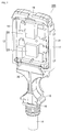
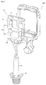
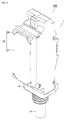
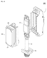
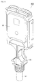
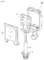
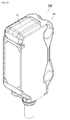
- FIG. 7 It is a perspective view of the substrate module for a photoelectric sensor which concerns on this embodiment. It is an exploded perspective view of the substrate module for a photoelectric sensor shown in FIG. It is a figure which looked at the substrate module for a photoelectric sensor shown in FIG. 1 from the front view. It is a figure which looked at the substrate module for a photoelectric sensor shown in FIG. 1 from the side view. It is sectional drawing of the substrate module for a photoelectric sensor along the VV line shown in FIG. It is sectional drawing of the substrate module for a photoelectric sensor along the VI-VI line shown in FIG. It is a perspective view of the substrate module for a photoelectric sensor which concerns on this embodiment. It is an exploded perspective view of the substrate module for a photoelectric sensor shown in FIG. 7.
- FIG. It is a perspective view of the substrate module for a photoelectric sensor which concerns on this embodiment. It is an exploded perspective view of the substrate module for a photoelectric sensor shown in FIG. It is a perspective view of the substrate module for a photoelectric sensor which concerns on this embodiment. It is an exploded perspective view of the substrate module for a photoelectric sensor shown in FIG. It is a perspective view of the side type photoelectric sensor which concerns on this embodiment. It is an exploded perspective view of the side type photoelectric sensor shown in FIG. It is a perspective view of the flat type photoelectric sensor which concerns on this embodiment. It is an exploded perspective view of the flat type photoelectric sensor shown in FIG. It is a perspective view of the photoelectric sensor which shows the direction which confirms the visibility in an Example.
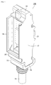
- FIG. 1 is a schematic view showing an outline of a photoelectric sensor substrate module 100 according to an embodiment of the present invention.
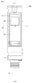
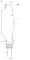
- FIG. 3 and FIG. 4 are an exploded perspective view, a front view, and a side view of the photoelectric sensor substrate module 100, respectively.
- 5 and 6 are cross-sectional views of the photoelectric sensor substrate module 100 along the VV line and the VI-VI line of FIGS. 3 and 4, respectively.
- the substrate module 100 for a photoelectric sensor can usually be used for a side type photoelectric sensor described later.
- the photoelectric sensor substrate module 100 includes a substrate 13, a mounting substrate 10 including an operation display unit 11 and a light receiving / receiving element 12 mounted on the substrate 13, and a part of the mounting substrate.
- the covering member 1 to be covered is included.
- the covering member 1 has a bottom surface 16, a side surface 17, a side surface 18, a top surface 19, a front surface 20, and a back surface 21.
- the front surface 20 is a surface on the side where light is projected and received by the light receiving and receiving element 12.
- the back surface 21 is positioned so as to face the front surface 20.
- the side surface 17, the side surface 18, the top surface 19, and the front surface 20 are also positioned so as to face each other.
- the coating member 1 is formed of a crystalline thermoplastic hot melt resin.
- having crystallinity means that the scattering region derived from the crystalline portion is confirmed in the X-ray diffraction information (wide-angle X-ray diffraction pattern or wide-angle X-ray diffraction profile) obtained by the X-ray diffraction method. Means.
- the free volume of the polymer constituting the crystalline thermoplastic hot melt resin becomes small, and oil (mineral oil) or aqueous solution (rust prevention) Agents, water, surfactants) are less likely to enter, but in general, it is estimated that the crystallinity tends to decrease because the crystal size of the crystalline part is larger than the wavelength of visible light. Will be done.
- the amorphous part since the polymer is coarsely aggregated, the free volume of the polymer becomes large, and oil (mineral oil) and aqueous solution (rust preventive, water, surfactant) invade. It is easy to use and is presumed to have translucency in the visible light region.
- the polymer itself may absorb light in part of the amorphous portion, it is considered that the visibility required for the photoelectric sensor is at a negligible level.
- the crystallinity of the thermoplastic hot-melt resin having crystallinity is 8% or more and 22% or less.
- the crystallinity of the thermoplastic hot melt resin having crystallinity is less than 8%, the oil resistance to cutting oil and the like is insufficient.
- the sealing member 1 and the mounting board 10 and the components are separated from each other in the substrate module, and the sealing is broken.
- the crystallinity of the thermoplastic hot-melt resin having crystallinity exceeds 22%, the translucency of the sealing member 1 is remarkably lowered, and the visibility of the indicator lamp (made of LED) is impaired. As a result, it becomes impossible to determine the operating state of the sensor.
- the degree of crystallization measured by the X-ray diffraction method is the scattering derived from the amorphous structure from the X-ray diffraction information (wide-angle X-ray diffraction pattern or wide-angle X-ray diffraction profile) obtained by irradiating the sample with X-rays.
- the region and the scattering region derived from the crystalline structure are separated and calculated as the ratio of the scattering intensity derived from the crystalline structure to the total scattering intensity.
- the X-ray diffraction method is based on JIS K0131 "General rules for X-ray diffraction analysis", and the measurement conditions are suitable for measuring the crystallinity of the thermoplastic hot melt resin according to the present embodiment.
- the crystallinity of the thermoplastic hot-melt resin having crystallinity is preferably 10% or more from the viewpoint of more stable oil resistance in consideration of variations in crystallinity depending on the mold temperature and the molding resin temperature. is there. Further, if the crystallinity of the thermoplastic hot-melt resin having crystallinity is high, the resin fluidity at the time of molding may be inferior, and the resin filling property in a narrow portion may be impaired. Therefore, 20% is preferable. It is as follows.
- the thermoplastic hot-melt resin having crystallinity may be any thermoplastic hot-melt resin having a crystal structure in the constituent molecular structure.
- examples thereof include polyester-based resins, polyamide-based resins, polyolefin-based resins, styrene-based resins, and polyurethane-based resins.
- polyester resins are preferable from the viewpoint of availability and moldability.
- the polyester resin may be, for example, a saturated copolymer polyester resin, and may be obtained mainly by polycondensation of a dibasic acid and glycol.
- Such a saturated copolymerized polyester resin is obtained by copolymerizing a main component such as polybutylene terephthalate or polyethylene terephthalate having crystallinity with an aliphatic acid or isophthalic acid as other components to adjust the crystallinity. You can.
- a main component such as polybutylene terephthalate or polyethylene terephthalate having crystallinity with an aliphatic acid or isophthalic acid as other components to adjust the crystallinity. You can.
- the thermoplastic hot melt resin having crystallinity commercially available ones can be used.
- the crystalline thermoplastic hot melt resin is solid at room temperature and may have a melting point in the range of, for example, 140 ° C. or higher and 200 ° C. or lower from the viewpoint of moldability.
- the crystalline thermoplastic hot-melt resin has other compositions such as polyester, polyamide, and polyolefin, as required, for the purpose of improving adhesiveness, flexibility, durability, etc., as long as the effects of the present invention are not impaired.
- Epoxy, acrylic, ethylene vinyl acetate, phenol and other resin components can be blended and used as a thermoplastic hot melt resin composition.
- the thermoplastic hot melt resin composition includes pigments such as carbon black, titanium oxide and calcium carbonate, fillers such as talc, silica and mica, dibutylhydroxytoluene (BHT), hindered phenol-based and sulfur-based stabilization.
- Additives such as agents, flame retardants such as antimony trioxide, aromatic phosphate ester and brominated diphenyl ether, and crystal nucleating agents such as aromatic carboxylic acid metal salt, aliphatic carboxylic acid metal salt and metal oxide are further added. You can also do it.
- the covering member 1 can be molded by arranging the mounting substrate 10 in a sealing mold having a substantially rectangular parallelepiped shape, and then filling the sealing mold with a thermoplastic hot-melt resin having crystallinity. At this time, the covering member 1 is molded so that the light emitting / receiving element 12 is exposed from the covering member 1. As a result, the light receiving and receiving by the light emitting and receiving element 12 is not hindered, and the influence of oil such as cutting oil on the operation display unit 11 and the electronic component 24 described later can be reduced. Further, since the covering member 1 is molded at a low temperature and a low pressure, the substrate 13 and the operation display unit 11 are less likely to be deformed by heat or pressure, and the alignment accuracy of the operation display unit 11 is less affected.
- the covering member 1 may have a through hole, a notch, a groove, a protrusion, or the like for joining with the mounting substrate 10, the protector 15, the cover portion 24, the housing 50, and the window 51, which will be described later.
- FIG. 5 is a cross-sectional view of the photoelectric sensor substrate module 100 along the VV line of FIG.
- FIG. 6 is a cross-sectional view of the photoelectric sensor substrate module 100 along the VI-VI line of FIG.
- the light emitting / receiving element 12 is exposed from the covering member 1, but the operation display unit 11 is covered with the covering member 1.
- the terminals connecting the operation display unit 11 and the substrate 13 are protected, and the operation display unit 11 is less susceptible to the influence of cutting oil, and as a result, excellent oil resistance is exhibited.
- the covering member 1 has a specific crystallinity to ensure translucency, the display of the operation status by the operation display unit 11 is recognized through the covering member 1 without the need for a light guide plate or the like. It is possible.
- the mounting board 10 a surface other than the surface on the mounting board 10 on which the light emitting / receiving element 12 is mounted and an operation display unit 11 are covered with a covering member 1. From the viewpoint of oil resistance, it is preferable that the mounting substrate 10 is entirely covered with the covering member 1 except for the light emitting and receiving element 12, and the surface of the light emitting and receiving element 12 on the front surface 20 side of the light emitting portion 22 and the light receiving portion 23. It is more preferable that all but the above are covered with the covering member 1.
- Electronic components 24 may be further mounted on the mounting board 10.
- the electronic component 24 is mounted on the back surface 21 side of the substrate 13, but it may be mounted on the front surface 20 side.
- the electronic component 24 may be, for example, a power supply, an amplifier unit, an electronic circuit, or the like.
- the substrate 13 may have through holes, notches, grooves, protrusions, and the like for joining the covering member 1 and the cover portion 24 described later.
- the operation display unit 11 displays the operation status of the photoelectric sensor.
- the operating status includes, for example, the power supply status and the detection status of the photoelectric sensor.
- the operation display unit 11 may be composed of a light emitting element such as a light emitting diode.
- the operation display unit 11 may be turned on when the power of the photoelectric sensor is turned on or when the photoelectric sensor detects a work. Further, the operation display unit 11 may turn on light of a different color depending on the type of work detected by the photoelectric sensor.
- the light emitting / receiving element 12 may be composed of a light emitting unit 22 and a light receiving unit 23.
- the light projecting unit 22 is a portion that emits light to the detection target.
- the light projecting unit 22 usually includes a light projecting element and a light projecting lens (not shown).
- the light projecting element may be, for example, a laser diode (LD) or a light emitting diode (LED). The light emitted from the light projecting element reaches the detection target through the light projecting lens.
- LD laser diode
- LED light emitting diode
- the light receiving unit 23 is a portion that detects the light reflected from the detection target.
- the light receiving unit 23 usually includes a light receiving element and a light receiving lens (not shown).
- the light receiving element may be, for example, a photodiode or a position detecting element. The light reflected from the detection target reaches the light receiving element through the light receiving lens.
- the photoelectric sensor substrate module 100 can further include an external connection member 14 and a protector 15.
- the external connection member 14 is a member that transmits electric power supplied from a power source to the photoelectric sensor substrate module 100, and houses a plurality of cords inside.
- the external connection member 14 can connect the photoelectric sensor substrate module 100 to an amplifier unit including an amplification unit, a control unit, and the like, and transmit the detection result by the photoelectric sensor substrate module 100.
- the external connecting member 14 may further have a connector for connecting to the amplifier unit.
- the external connecting member 14 is connected to the bottom surface 16 of the photoelectric sensor 100, but the connection position does not necessarily have to be the bottom surface 16, and may be connected to the side surface 17 or the side surface 18. At least one of the power supply and the amplifier unit may be built in the photoelectric sensor substrate module 100.
- the contact point between the cord housed inside the external connecting member 14 and the mounting substrate 10 is covered with the covering member 1.
- the photoelectric sensor substrate module 100 may include a protector 15.
- the protector 15 is provided at a connecting portion between the covering member 1 and the external connecting member 14. In the external connecting member 14, the connection portion with the covering member 1 is likely to be loaded by bending the external connecting member 14. The protector 15 prevents the external connecting member 14 from being excessively bent and prevents the external connecting member 14 from being damaged.
- the photoelectric sensor substrate module 200 can be used for a flat type photoelectric sensor.
- the operation display unit 11 is covered with the sealing member 1.
- the photoelectric sensor substrate module 200 can exhibit excellent oil resistance.
- the mounting substrate 10 further includes the electronic component 24 on the surface on which the light emitting / receiving element 12 is mounted.
- the thickness of the photoelectric sensor substrate module 200 can be reduced from the front surface 20 to the back surface 21 direction as compared with the photoelectric sensor substrate module 100.
- the photoelectric sensor substrate module 100 and the photoelectric sensor substrate module 200 can be manufactured as follows. First, the operation display unit 11 and the light receiving / receiving element 12 are mounted on the substrate 13 to obtain the mounting substrate 10. Next, the external connecting member 14 is connected to the mounting board 10, and the protector 15 is mounted on the external connecting member 14. After that, the mounting substrate 10 is placed in the sealing mold. At this time, it is preferable that the connecting portion between the mounting substrate 10 and the external connecting member 14 is arranged in the sealing mold.
- the mold can have a structure in which the light emitting / receiving element 12 is exposed from the covering member 1.
- a thermoplastic hot-melt resin having crystallinity is press-fitted into the sealing mold to mold the coating member 1 and cool it. Finally, the protector 15 is attached to the covering member 1.
- the crystalline thermoplastic hot melt resin can be molded at a temperature of, for example, 140 ° C. or higher and 200 ° C. or lower, and a pressure of, for example, 10 MPa or lower.
- the substrate module 300 for a photoelectric sensor can be used for a side type photoelectric sensor.
- FIG. 11 and 12 are a schematic view and an exploded perspective view showing an outline of the photoelectric sensor substrate module 400 according to another embodiment, respectively.
- the substrate module 400 for a photoelectric sensor can be used for a flat type photoelectric sensor.
- the photoelectric sensor substrate module 300 and the photoelectric sensor substrate module 400 include a cover portion 25, an external connection member 14, and a protector 15.
- the cover portion 25 is installed at a position facing the light receiving / receiving element 12.
- the cover portion 25 may be composed of the cover 27 and the holder 26, or the cover 27 and the holder 26 may be integrally molded.
- the cover portion 25 is exposed from the covering member 1 so as not to interfere with the emission of light and the detection of light by the light emitting / receiving element 12. From the viewpoint of oil resistance, the cover portion 25 is preferably at least partially covered with the sealing member 1.
- the cover portion 25 of the substrate module for the photoelectric sensor and 400 it is possible to achieve both the optical visibility and the oil resistance of the light emitting element required for the photoelectric sensor, and the light emitting and receiving element 12 is covered by the cover portion 25. Further, by adhering the cover portion 25 with the thermoplastic hot melt resin, the influence of cutting oil and dust on the light receiving and receiving element 12 can be reduced.
- the cover portion 25 and the cover 27 may be made of a material that transmits light emitted from the light projecting portion and light reflected from the detection target, for example, a translucent resin or glass.
- the light emitted from the light projecting unit reaches the detection target through the cover 27. Further, the light reflected from the detection target reaches the light receiving portion through the cover 27.
- the holder 26 can be supported by the mounting substrate 10 and the sealing member 1.
- the photoelectric sensor substrate module 300 and the photoelectric sensor substrate module 400 can be manufactured as follows. First, the operation display unit 11 and the light receiving / receiving element 12 are mounted on the substrate 13 to obtain the mounting substrate 10. Next, the external connecting member 14 is connected to the mounting board 10, and the protector 15 is mounted on the external connecting member 14. After that, the mounting substrate 10 to which the cover portion 25 is attached is arranged in the sealing mold. At this time, it is preferable that the connecting portion between the mounting substrate 10 and the external connecting member 14 is arranged in the sealing mold.
- the mold can have a structure in which the light emitting / receiving element 12 is exposed from the covering member 1. Next, a crystalline thermoplastic hot-melt resin is press-fitted into the sealing die to mold the coating member 1 and cool it. Finally, the protector 15 is attached to the covering member 1.
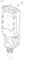
- FIG. 13 is a schematic view showing an outline of the side type photoelectric sensor 500.
- the photoelectric sensor 500 includes a substrate module for the photoelectric sensor, a housing 50, and a window 51.
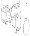
- FIG. 14 is an exploded perspective view of the photoelectric sensor 500.
- the photoelectric sensor 500 includes the above-mentioned photoelectric sensor substrate module 200, the first member 50a, the second member 50b, and the window 51.
- the photoelectric sensor substrate module 200 includes a cover portion 25, an external connection member 14, and a protector 15.
- FIG. 15 is a schematic view showing an outline of the flat type photoelectric sensor 600.
- the photoelectric sensor 600 includes a substrate module for the photoelectric sensor, a housing 50, and a window 51.
- FIG. 16 is an exploded perspective view of the photoelectric sensor 600.
- the photoelectric sensor 600 includes the above-mentioned photoelectric sensor substrate module 400, a first member 50a, a second member 50b, and a window 51.
- the photoelectric sensor substrate module 400 includes a cover portion 25, an external connection member 14, and a protector 15.
- the housing 50 protects various parts such as the photoelectric sensor substrate module contained inside the photoelectric sensors 500 and 600 from impact and dirt.
- the housing 50 is made of metal, resin, or the like.
- the window 51 protects the operation display unit provided inside the substrate module for the photoelectric sensor from impact and dirt, and displays the operation status of the photoelectric sensor.
- the window 51 may be made of a material through which light from the operation display unit is transmitted, for example, a translucent resin or glass. Visibility can be improved by coloring the window 51. Further, by coloring the window 51 for each operation display unit, it is possible to easily confirm the operation status.
- the first member 50a is combined with the second member 50b to form the housing 50.
- the first member 50a has a hollow inside, and is formed so that a substrate module for a photoelectric sensor can be accommodated.
- the second member 50b is combined with the first member 50a to form the housing 50.
- the combination of the first member 50a and the second member 50b may be performed by welding, the use of an adhesive, or the like.
- the photoelectric sensors 500 and 600 can be manufactured as follows. First, the substrate module for the photoelectric sensor is housed in the first member 50a. Next, the window 51 is attached to the upper part of the board module for the photoelectric sensor. After that, the first member 50a is combined with the second member 50b. The combination of the first member 50a and the second member 50b may be performed by welding, the use of an adhesive, or the like.
- thermoplastic hot-melt resin for which the degree of crystallinity was measured was molded into a cube (length of each side 5 mm) under the molding conditions in each Example or Comparative Example to prepare a sample for measurement.
- Each sample was placed in a standard holder, and an X-ray diffraction pattern was obtained by wide-angle X-ray diffraction.
- the measuring device and conditions are shown below.
- the oil resistance was evaluated by immersing the substrate module for the photoelectric sensor in cutting oil. Specifically, it is immersed in an oil bath at 50 ° C. containing a water-insoluble cutting oil (JIS N class coolant) or a water-soluble cutting oil (JIS A class 1 coolant (diluted 30 times with water)) for 100 hours.
- JIS N class coolant a water-insoluble cutting oil
- JIS A class 1 coolant diluted 30 times with water
- a two-step evaluation was performed in which the insulation resistance value exceeding 50 M ⁇ was evaluated as “ ⁇ ” and the insulation resistance value of 50 M ⁇ or less was evaluated as “x”.
- a Megohm HiTester 3453 (manufactured by Hioki Electric Co., Ltd.) was used to measure the insulation resistance value.
- Example 1 A substrate module for a photoelectric sensor was molded using a polyester-based resin a1 (crystallinity: 12%) as a thermoplastic hot-melt resin having crystallinity.
- a molding machine a Canon Electronics molding machine LS-300i was used.
- the assembly intermediate product was inserted into a mold and molded and sealed under the following molding conditions to obtain a substrate module for a photoelectric sensor.
- the molding conditions were a resin temperature of 240 ° C., a molding pressure of 10 MPa, a mold temperature of 50 ° C., and a cooling time of 60 sec.
- a housing and a window were attached to the above-mentioned substrate module for a photoelectric sensor to obtain a finished product of the photoelectric sensor.
- An oil resistance test and a visibility test were performed using the photoelectric sensor. The results are shown in Table 1.
- Example 2 The photoelectric sensor finished product of Example 2 was prepared in the same manner as in Example 1 except that the polyester resin a2 (crystallinity: 8%) was used instead of the polyester resin a1 in Example 1. Obtained. The results of the oil resistance test and the visibility test are shown in Table 1.
- Example 3 The photoelectric sensor finished product of Example 3 was prepared in the same manner as in Example 1 except that the polyester resin a3 (crystallinity: 22%) was used instead of the polyester resin a1 in Example 1. Obtained. The results of the oil resistance test and the visibility test are shown in Table 1.
- Comparative Example 1 The photoelectric sensor finished product of Comparative Example 1 was prepared in the same manner as in Example 1 except that the polyester resin b1 (crystallinity: 6%) was used instead of the polyester resin a1 in Example 1. Obtained. The results of the oil resistance test and the visibility test are shown in Table 1.
- Comparative Example 2 The photoelectric sensor finished product of Comparative Example 2 was prepared in the same manner as in Example 1 except that the polyester resin b2 (crystallinity: 25%) was used instead of the polyester resin a1 in Example 1. Obtained. The results of the oil resistance test and the visibility test are shown in Table 1.
- the covering member (1) is formed so as to cover the operation display unit (11) and expose the light emitting / receiving element (12) from the covering member (1).
- the coating member (1) is a substrate module for a photoelectric sensor, which is formed of a thermoplastic hot-melt resin having crystallinity and has a crystallinity of 8% or more and 22% or less as measured by an X-ray diffraction method.
- a cover portion (25) installed at a position facing the light receiving / receiving element (12) is further included.
- Sealing member 10 Mounting board, 11 Operation display unit, 12 Light receiving element, 13 Board, 14 External connection member, 15 Protector, 16 Bottom, 17, 18 Side, 19 Top, 20 Front, 21 Back, 22 Flood Part, 23 light receiving part, 24 electronic parts, 25 cover part, 26 holder, 27 cover, 50 housing, 50a first member, 50b second member, 51 window, 100, 200, 300, 400 board module for photoelectric sensor, 500,600 photoelectric sensor.
Landscapes
- Switches Operated By Changes In Physical Conditions (AREA)
Abstract
基板、ならびに、基板に実装された動作表示部および投受光素子を含む実装基板と、実装基板の一部を被覆する被覆部材とを含む基板モジュールであって、被覆部材は、動作表示部を被覆し、かつ、投受光素子が被覆部材から露出するように形成されており、被覆部材は、結晶性を有する熱可塑性ホットメルト樹脂から形成され、X線回折法で計測される結晶化度が8%以上、22%以下である光電センサ用基板モジュール。
Description
本技術は、光電センサ用基板モジュールおよび光電センサに関する。
製造搬送ラインや部品加工機に用いられる場合が多い光電センサは、防水性および防塵性の観点から、光電センサの筐体嵌合部が接着剤等で封止される場合がある。しかしながら、このような光電センサは、組立工程が煩雑で、かつ接着剤硬化時間が長く、生産性に欠ける。
別の封止手法として、エンジニアリングプラスチックのような熱可塑性樹脂を用いて成型封止する方法が知られている。しかしながら、光学部品や基板が内蔵された光電センサでは、熱可塑性樹脂の成形温度や圧力により、前記内蔵部品にダメージが発生する場合がある。
そこで、特開2014-32805号公報(特許文献1)には、比較的低温および低圧で成型可能なホットメルトと呼ばれる熱可塑性樹脂を用いて光学部品や基板を成型封止する方法が提案されている。このような熱可塑性樹脂として、例えば特開2006-312679号公報(特許文献2)に記載のようなポリエステル系樹脂が知られている。
近年、熱可塑性樹脂で成型封止された光電センサは、IP67を指標とする耐水性に加えて、切削油等に対する耐油性が求められている。
一般に、成形封止には、実装される動作表示部や投受光素子、他の樹脂製部品への熱ダメージおよび応力ダメージを低減する目的で、比較的低温および低圧で、例えば140℃以上200℃以下の温度および10MPa以下の圧力で射出成形機やアプリケーターにより成型可能な熱可塑性ホットメルト樹脂が用いられる。
また、成型封止には、金属や各種プラスチックスへの接着性に優れ、衝撃を吸収し易い熱可塑性ホットメルト樹脂が用いられることが多い。例えばこのような熱可塑性ホットメルト樹脂で成型封止された光電センサは、設備の振動などが光電センサに加わった場合でも、部品同士の接合等が維持され、熱可塑性ホットメルト樹脂がその振動を吸収し、基板や動作表示部、投受光素子および電子部品に振動ダメージが及ばず、光電センサの破損を防止することができる。
しかしながら、このような熱可塑性ホットメルト樹脂は、汎用プラスチックと比較して、耐油性に劣る場合が多い。このため、鉱物油、界面活性剤、防錆剤、および水などからなる切削油に長時間浸漬すると、熱可塑性のホットメルト樹脂が切削油を吸収し、膨潤し、その結果、接着封止部が剥がれ、製品の動作不良に至る場合がある。ゆえに、耐油性が求められる使用環境では、熱可塑性ホットメルト樹脂で成型封止した電子機器は適合しない場合がある。
本発明者によって、成形封止に用いられる熱可塑性ホットメルト樹脂は、一般的なエンジニアリングプラスチックのように高分子鎖が緻密ではなく、比較的自由体積が大きい高分子鎖で構成されているため耐油性に劣ることが突止められた。耐油性の向上について研究を行った結果、熱可塑性ホットメルト樹脂に結晶構造を導入することで、切削油による膨潤が抑制されることが見出された。
一方、そのような結晶性を有する熱可塑性ホットメルト樹脂は、結晶化度が余りに高い場合、樹脂自体が透光性を有しなくなることが分かった。この場合、光電センサに発光部を備えた動作表示部があると、動作表示が不透明な熱可塑性ホットメルト樹脂で被覆されるため、発光部が認識できなくなる。このような場合、例えば特許文献1に記載のような導光部品を用いて動作表示部からの光を導出する必要がある。
すなわち、耐油性向上の観点から熱可塑性ホットメルト樹脂の結晶化率を高くすると、結晶構造によって樹脂は透光性を有しなくなり、発光素子の光視認性が毀損されるという問題が生じ、発光素子の光視認性を高めるために熱可塑性ホットメルト樹脂の結晶化率を下げると、耐油性が毀損されるという問題が生じる。
この開示の一つの目的は、光電センサとして要求される耐油性と発光素子の光視認性を両立する、熱可塑性ホットメルト樹脂で成型封止された光電センサ用基板モジュールを提供することである。
本開示の一例では、光電センサ用基板モジュールは、基板、ならびに基板に実装された動作表示部および投受光素子を含む実装基板と、実装基板の一部を被覆する被覆部材とを含む基板モジュールであって、被覆部材は、動作表示部を被覆し、かつ、投受光素子が被覆部材から露出するように形成されており、被覆部材は、結晶性を有する熱可塑性ホットメルト樹脂から形成され、X線回折法で計測される結晶化度が8%以上、22%以下である。
この開示によれば、光電センサ用基板モジュールにおいて、動作表示部が透光性を有し、かつ耐油性を有する熱可塑性ホットメルト樹脂で被覆されているため、光電センサとして要求される発光素子の光視認性と耐油性とを両立することができる。
本開示の一例では、投受光素子と対面する位置に設置されるカバー部をさらに含み、カバー部は少なくとも一部が被覆部材から露出している。
この開示によれば、光電センサとして要求される発光素子の光視認性と耐油性とを両立することができるとともに、投受光素子がカバー部により覆われ、さらに当該カバー部が熱可塑性のホットメルト樹脂で接着されることで、投受光素子に対する切削油や埃の影響を低減することができる。
本開示の一例では、結晶性を有する熱可塑性ホットメルト樹脂はポリエステル系樹脂である。この開示によれば、結晶性を有する熱可塑性ホットメルト樹脂の入手可能性および成型性を高めることができる。
本開示の一例では、実装基板は、基板に実装された電子部品をさらに含む。この開示によれば、電子部品も結晶性を有する熱可塑性ホットメルト樹脂により成型封止されるため、光電センサ用基板モジュールの耐油性をより一層高めることができる。
本開示の一例では、上述の開示における光電センサ用基板モジュールは、外部接続部材をさらに備える。この開示によれば、光電センサを装置等に設置し易くすることができる。
本開示の一例では、光電センサは、上述の開示における光電センサ用基板モジュールと、筐体と、ウインドウとを備える。この開示によれば、筐体により光電センサ内部に含まれる光電センサ用基板モジュール等の各種部品が衝撃や汚れから保護され、ウインドウにより視認性を高めることができる。
この開示によれば、熱可塑性ホットメルト樹脂で成型封止された光電センサ用基板モジュールにおいて、光電センサとして要求される耐油性と発光素子の光視認性を両立することができる。
本発明の実施の形態について、図面を参照しながら詳細に説明する。なお、図中の同一または相当部分については、同一符号を付してその説明は繰り返さない。
<適用例>
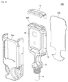
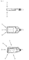
まず、図1~6を参照して、本発明が適用される場面の一例について説明する。図1は、本発明の実施形態に係る光電センサ用基板モジュール100の概要を示す模式図である。図2、図3及び図4はそれぞれ、光電センサ用基板モジュール100の分解斜視図、正面から見た図、側面から見た図である。図5及び図6はそれぞれ、図3及び図4のV-V線およびVI-VI線に沿った光電センサ用基板モジュール100の断面図である。
まず、図1~6を参照して、本発明が適用される場面の一例について説明する。図1は、本発明の実施形態に係る光電センサ用基板モジュール100の概要を示す模式図である。図2、図3及び図4はそれぞれ、光電センサ用基板モジュール100の分解斜視図、正面から見た図、側面から見た図である。図5及び図6はそれぞれ、図3及び図4のV-V線およびVI-VI線に沿った光電センサ用基板モジュール100の断面図である。
光電センサ用基板モジュール100は通常、後述するサイドタイプの光電センサに用いることができる。
図1および図2に示すように、光電センサ用基板モジュール100は、基板13、ならびに、基板13に実装された動作表示部11および投受光素子12を含む実装基板10と実装基板の一部を被覆する被覆部材1を含む。被覆部材1は、底面16、側面17、側面18、頂面19、前面20および背面21を有している。前面20は、投受光素子12により投受光される側の面である。背面21は、前面20に対向するように位置している。側面17および側面18、頂面19および前面20もそれぞれ対向するように位置している。
被覆部材1は、結晶性を有する熱可塑性ホットメルト樹脂から形成される。本明細書において、結晶性を有するとは、X線回折法により得られるX線回折情報(広角X線回折図形または広角X線回折プロファイル)において結晶質部分に由来する散乱領域が確認されることを意味する。
結晶質部分は、高分子が折り畳み構造で密に凝集しているため、結晶性を有する熱可塑性ホットメルト樹脂を構成する高分子の自由体積は小さくなり、油(鉱物油)や水溶液(防錆剤、水、界面活性剤)が侵入し難くなるが、一般的に、結晶質部分は結晶サイズが可視光の波長以上の大きさを有することから、透光性は低下する傾向にあると推定される。これに対し、非晶質部分は、高分子が粗に凝集しているため、高分子の自由体積は大きくなり、油(鉱物油)や水溶液(防錆剤、水、界面活性剤)が侵入し易く、可視光領域では透光性を有すると推定される。なお、非晶質部分は一部、高分子自体が光を吸収する場合もあるが、光電センサに要求される視認性においては、無視できるレベルにあると考えられる。
このようなことから、結晶性を有する熱可塑性ホットメルト樹脂の結晶化度は、8%以上、22%以下である。結晶性を有する熱可塑性ホットメルト樹脂は、結晶化度が8%を下回ると、切削油等に対し、耐油性が不足する。その結果、基板モジュール内において、封止部材1と実装基板10や構成部品とが剥離し、封止が破壊される。一方、結晶性を有する熱可塑性ホットメルト樹脂の結晶化度が22%を上回ると、封止部材1の透光性が著しく低下し、表示灯(LED製)の視認性が損なわれる。その結果、センサの動作状態を判別することができなくなる。
X線回折法で計測される結晶化度は、試料にX線を照射し、得られるX線回折情報(広角X線回折図形または広角X線回折プロファイル)から、非晶質構造に由来する散乱領域と結晶質構造に由来する散乱領域とを分け、全散乱強度に対する結晶質構造に由来する散乱強度の比として計算される。X線回折法は、JIS K0131「X線回折分析通則」に準拠し、本実施の形態に係る熱可塑性ホットメルト樹脂の結晶化度測定に適する測定条件とした。
結晶性を有する熱可塑性ホットメルト樹脂の結晶化度は、金型温度や成型樹脂温度による結晶化度のバラつきを考慮し、より安定的に耐油性を発現する観点から、好ましくは10%以上である。また、結晶性を有する熱可塑性ホットメルト樹脂の結晶化度が高いと成型時の樹脂流動性が劣る場合があり、狭小部への樹脂充填性が損なわれる場合があることから、好ましくは20%以下である。
結晶性を有する熱可塑性ホットメルト樹脂は、構成する分子構造中に結晶構造を有する熱可塑性ホットメルト樹脂であればよい。その例としては、ポリエステル系樹脂、ポリアミド系樹脂、ポリオレフィン系樹脂、スチレン系樹脂、ポリウレタン系樹脂などが挙げられる。中でも、入手可能性および成型性の観点から好ましくは、ポリエステル系樹脂が好ましい。ポリエステル系樹脂は、例えば飽和共重合ポリエステル系樹脂であってよく、主として二塩基性酸とグリコールとの重縮合等により得られるものであってよい。このような飽和共重合ポリエステル系樹脂は、結晶性を有するポリブチレンテレフタレートやポリエチレンテレフタレート等の主成分に、他成分として脂肪族酸やイソフタル酸などを共重合して結晶性を調整したものであってよい。結晶性を有する熱可塑性ホットメルト樹脂は、市販されているものを用いることができる。
結晶性を有する熱可塑性ホットメルト樹脂は、常温で固体であり、成型性の観点から例えば140℃以上200℃以下の範囲に融点を有するものであってよい。
結晶性を有する熱可塑性ホットメルト樹脂は、接着性、柔軟性、耐久性等を改良する目的で、本発明の効果を毀損しない範囲において、必要に応じて、その他の組成のポリエステル、ポリアミド、ポリオレフィン、エポキシ、アクリル、エチレンビニルアセテート、フェノール等の他の樹脂成分を配合して熱可塑性ホットメルト樹脂組成物として用いることもできる。熱可塑性ホットメルト樹脂組成物には、カーボンブラック、酸化チタン、炭酸カルシウム等の顔料、タルク、シリカ、雲母等の充鎮材、ジブチルヒドロキシトルエン(BHT)、ヒンダードフェノール系、硫黄系の安定化剤、三酸化アンチモン、芳香族リン酸エステル、臭素化ジフェニルエーテル等の難燃剤、芳香族カルボン酸金属塩、脂肪族カルボン酸金属塩、金属酸化物等の結晶核剤等の添加剤をさらに配合することもできる。
被覆部材1は、略直方体形状の封止用金型に実装基板10を配置した後、結晶性を有する熱可塑性ホットメルト樹脂を封止用金型に充填することにより成型することができる。このとき、被覆部材1は、投受光素子12が被覆部材1から露出するように成型される。これにより、投受光素子12による投受光は妨げられることがなく、かつ動作表示部11や後述する電子部品24等に対する切削油等の油の影響を受けにくくすることができる。また、被覆部材1は、低温かつ低圧で成型されるため、熱や圧力による基板13や動作表示部11の変形が生じにくく、動作表示部11のアライメント精度への影響が少ない。
被覆部材1は、実装基板10やプロテクタ15、後述するカバー部24、筐体50、ウインドウ51との接合のための貫通孔や切欠き、溝、突起等を有していてよい。
図5は、図3のV-V線に沿った光電センサ用基板モジュール100の断面図である。図6は、図4のVI-VI線に沿った光電センサ用基板モジュール100の断面図である。図5および図6に示されるように、投受光素子12は被覆部材1から露出しているが、動作表示部11は被覆部材1により被覆されている。これにより、動作表示部11と基板13とを接続する端子が保護され、動作表示部11についての切削油の影響を受け難くなり、その結果、優れた耐油性が発揮されることとなる。また、被覆部材1が特定の結晶化度を有することにより透光性が確保されるため、動作表示部11による動作状況の表示を被覆部材1を通して、導光板等を必要とすることなく認識することが可能である。
実装基板10は、実装基板10の投受光素子12が実装されている側の面以外の面と動作表示部11とが被覆部材1で被覆されている。実装基板10は、耐油性の観点から、投受光素子12以外の全部が被覆部材1で被覆されていることが好ましく、投受光素子12の投光部22および受光部23の前面20側の面以外の全部が被覆部材1で被覆されていることがより好ましい。
実装基板10は、電子部品24がさらに実装されていてもよい。光電センサモジュール100は、電子部品24が基板13の背面21側に実装されているが、前面20側に実装されていてもよい。電子部品24は、例えば電源やアンプユニット、電子回路等であってよい。基板13は、被覆部材1や後述するカバー部24との接合のための貫通孔や切欠き、溝、突起等を有していてもよい。
動作表示部11は、光電センサの動作状況を表示する。動作状況には、例えば光電センサの電源状況や検出状況等が含まれる。動作表示部11は、例えば発光ダイオード等の発光素子で構成されていてもよい。動作表示部11は、光電センサの電源がONになっている場合や光電センサがワークを検出した場合に点灯してもよい。また、動作表示部11は、光電センサが検出したワークの種類に応じて異なった色の光を点灯してもよい。
投受光素子12は、投光部22および受光部23から構成されていてよい。投光部22は、検出対象へと光を出射する部分である。投光部22は通常、投光素子及び投光レンズを備える(図示せず)。投光素子は、例えばレーザーダイオード(LD)や発光ダイオード(LED)であってよい。投光素子から出射された光は、投光レンズを通って検出対象に到達する。
受光部23は、検出対象から反射された光を検出する部分である。受光部23は通常、受光素子及び受光レンズを備える(図示せず)。受光素子は、例えば受光素子は、例えばフォトダイオードや位置検出素子であってよい。検出対象から反射した光は、受光レンズを通って受光素子へ到達する。
光電センサ用基板モジュール100は、外部接続部材14およびプロテクタ15をさらに備えることができる。
外部接続部材14は、電源から供給される電力を光電センサ用基板モジュール100へ送電する部材であり、内部に複数のコードを収容する。外部接続部材14は、光電センサ用基板モジュール100を増幅部及び制御部等を含むアンプユニットに接続し、光電センサ用基板モジュール100による検出の結果を伝達することができる。外部接続部材14はアンプユニットへ接続するためのコネクタをさらに有していてもよい。本例において、外部接続部材14は光電センサ100の底面16に接続されているが、接続位置は必ずしも底面16でなくともよく、側面17又は側面18等に接続されてもよい。なお、電源及びアンプユニットの少なくともいずれかは、光電センサ用基板モジュール100に内蔵されていてもよい。
耐油性の観点から好ましくは外部接続部材14内部に収容されるコードと実装基板10との接点が被覆部材1により被覆されていることが好ましい。
光電センサ用基板モジュール100は、プロテクタ15を備えていてもよい。プロテクタ15は、被覆部材1と外部接続部材14との接続部分に設けられている。外部接続部材14は、被覆部材1との接続部分が外部接続部材14の折り曲げにより負荷がかかりやすい。プロテクタ15は、外部接続部材14の過度な折り曲げを防ぎ、外部接続部材14の破損を防止する。
図7および図8はそれぞれ、光電センサ用基板モジュール200の概要を示す模式図および分解斜視図である。光電センサ用基板モジュール200は、フラットタイプの光電センサに用いることができる。
光電センサ用基板モジュール200においても、動作表示部11は封止部材1により被覆されている。これにより、光電センサ用基板モジュール200は、優れた耐油性を発揮することができる。
光電センサ用基板モジュール200において、実装基板10は、電子部品24を投受光素子12が実装された面にさらに含む。これにより光電センサ用基板モジュール200は、光電センサ用基板モジュール100に比べ前面20から背面21方向への厚みを小さくすることができる。
光電センサ用基板モジュール100および光電センサ用基板モジュール200は、次のようにして製造することができる。まず、基板13に動作表示部11および投受光素子12を実装して実装基板10を得る。次に実装基板10に外部接続部材14を接続し、外部接続部材14にプロテクタ15を装着する。その後、実装基板10を封止用金型内に配置する。このとき、実装基板10と外部接続部材14との接続部が封止用金型内に配置されることが好ましい。金型は、投受光素子12が被覆部材1から露出するような構造を有することができる。次いで、封止用金型内に結晶性を有する熱可塑性ホットメルト樹脂圧入し、被覆部材1を成型し、冷却する。最後にプロテクタ15を被覆部材1に取り付ける。結晶性を有する熱可塑性ホットメルト樹脂は、例えば140℃以上200℃以下の温度、および例えば10MPa以下の圧力で成型することができる。
図9および図10はそれぞれ、光電センサ用基板モジュール300の概要を示す模式図および分解斜視図である。光電センサ用基板モジュール300は、サイドタイプの光電センサに用いることができる。
図11および図12はそれぞれ、別の実施の形態に係る光電センサ用基板モジュール400の概要を示す模式図および分解斜視図である。光電センサ用基板モジュール400は、フラットタイプの光電センサに用いることができる。
光電センサ用基板モジュール300および光電センサ用基板モジュール400は、カバー部25、外部接続部材14およびプロテクタ15を備える。カバー部25は、投受光素子12と対面する位置に設置される。カバー部25は、カバー27およびホルダ26から構成されていてもよいし、カバー27およびホルダ26が一体成型されたものであってもよい。
カバー部25は少なくとも一部が、投受光素子12による光の射出および光の検出が妨げられないように被覆部材1から露出している。カバー部25は、耐油性の観点から好ましくは、少なくとも一部が封止部材1により被覆されている。光電センサ用基板モジュールおよび400はカバー部25を備えることにより、光電センサとして要求される発光素子の光視認性と耐油性とを両立することができるとともに、投受光素子12がカバー部25により覆われ、さらにカバー部25が熱可塑性ホットメルト樹脂で接着されることで、投受光素子12に対する切削油や埃の影響を低減することができる。
カバー部25およびカバー27は、投光部から出射される光および検出対象から反射した光を透過する材質、例えば透光性を有する樹脂やガラス等で形成されていてよい。投光部から出射される光は、カバー27を通って検出対象へ到達する。また、検出対象から反射した光は、カバー27を通って受光部へ到達する。ホルダ26は、実装基板10や封止部材1により支持されることができる。
光電センサ用基板モジュール300および光電センサ用基板モジュール400は、次のようにして製造することができる。まず、基板13に動作表示部11および投受光素子12を実装して実装基板10を得る。次に実装基板10に外部接続部材14を接続し、外部接続部材14にプロテクタ15を装着する。その後、カバー部25を取り付けた実装基板10を封止用金型内に配置する。このとき、実装基板10と外部接続部材14との接続部が封止用金型内に配置されることが好ましい。金型は、投受光素子12が被覆部材1から露出するような構造を有することができる。次いで、封止用金型内に結晶性を有する熱可塑性ホットメルト樹脂を圧入し、被覆部材1を成型し、冷却する。最後にプロテクタ15を被覆部材1に取り付ける。
<光電センサ用基板モジュールが適用される光電センサの一例>
図13は、サイドタイプの光電センサ500の概要を示す模式図である。光電センサ500は、光電センサ用基板モジュール、筐体50およびウインドウ51を備える。
図13は、サイドタイプの光電センサ500の概要を示す模式図である。光電センサ500は、光電センサ用基板モジュール、筐体50およびウインドウ51を備える。
図14は、光電センサ500の分解斜視図である。光電センサ500は、上述の光電センサ用基板モジュール200、第1部材50a、第2部材50bおよびウインドウ51を備える。光電センサ用基板モジュール200は、カバー部25、外部接続部材14およびプロテクタ15を備える。
図15は、フラットタイプの光電センサ600の概要を示す模式図である。光電センサ600は、光電センサ用基板モジュール、筐体50およびウインドウ51を備える。
図16は、光電センサ600の分解斜視図である。光電センサ600は、上述の光電センサ用基板モジュール400、第1部材50a、第2部材50bおよびウインドウ51を備える。光電センサ用基板モジュール400は、カバー部25、外部接続部材14およびプロテクタ15を備える。
筐体50は、光電センサ500および600内部に含まれる光電センサ用基板モジュール等の各種部品を衝撃や汚れから保護する。筐体50は、金属又は樹脂等で形成されている。
ウィンドウ51は、光電センサ用基板モジュール内部に設けられた動作表示部を衝撃や汚れから保護すると共に、光電センサの動作状況を表示する。ウィンドウ51は、動作表示部からの光が透過する材料、例えば透光性を有する樹脂やガラス等で形成されていてよい。ウィンドウ51を着色することにより視認性を高めることができる。また、動作表示部ごとにウィンドウ51を着色することにより動作状況を確認し易くすることができる。
第1部材50aは、第2部材50bと組み合わされて筐体50を形成する。第1部材50aは内部が空洞になっており、光電センサ用基板モジュールが収容できるように形成されている。
第2部材50bは、第1部材50aと組み合わされて筐体50を形成する。第1部材50aの内部に光電センサ用基板モジュールを配置した後、第1部材50aに第2部材50bを組み合わせることにより、光電センサ用基板モジュールが収容された筐体50を形成することができる。第1部材50aと第2部材50bとの組み合わせは、溶接又は接着剤の使用等により行われてもよい。
光電センサ500および600は、次のようにして製造することができる。まず、光電センサ用基板モジュールを第1部材50aに収容する。次にウインドウ51を光電センサ用基板モジュールの上部に取り付ける。その後、第1部材50aに第2部材50bを組み合わせる。第1部材50aと第2部材50bの組み合わせは、溶接又は接着剤の使用等により行われてもよい。
以下、実施例により本開示をさらに詳細に説明する。例中の「%」および「部」は、特記のない限り、質量%および質量部である。
[結晶化度]
結晶化度を測定する各熱可塑性ホットメルト樹脂をそれぞれの実施例または比較例における成型条件にて立方体(各辺の長さ5mm)に成型し、測定用試料とした。各試料を標準ホルダーに設置し、広角X線回折法によりX線回折パターンを得た。以下に測定装置および条件を示す。
(1)X線回折装置:Bruker AXS社製 D8 ADVANCE(封入管型)
X線源:CuKα線(Niフィルター使用)
出力:40kV、40mA
スリット系:Div.Slit:0.3°
検出器:LynxEye(高速検出器)
(2)スキャン方式:2θ/θ連続スキャン
(3)測定範囲(2θ):5~70°
(4)ステップ幅(2θ):0.0171°
(5)計数時間:0.5秒/ステップ
得られたX線回折パターンに対して、各ピーク分離を行い、各ピークデータから結晶質部分と非晶質部分との各ピーク面積(積分強度)を算出し、以下の式より結晶化度を算出した。
結晶化度を測定する各熱可塑性ホットメルト樹脂をそれぞれの実施例または比較例における成型条件にて立方体(各辺の長さ5mm)に成型し、測定用試料とした。各試料を標準ホルダーに設置し、広角X線回折法によりX線回折パターンを得た。以下に測定装置および条件を示す。
(1)X線回折装置:Bruker AXS社製 D8 ADVANCE(封入管型)
X線源:CuKα線(Niフィルター使用)
出力:40kV、40mA
スリット系:Div.Slit:0.3°
検出器:LynxEye(高速検出器)
(2)スキャン方式:2θ/θ連続スキャン
(3)測定範囲(2θ):5~70°
(4)ステップ幅(2θ):0.0171°
(5)計数時間:0.5秒/ステップ
得られたX線回折パターンに対して、各ピーク分離を行い、各ピークデータから結晶質部分と非晶質部分との各ピーク面積(積分強度)を算出し、以下の式より結晶化度を算出した。

[耐油性評価]
耐油性は光電センサ用基板モジュールを切削油に浸漬することで評価した。具体的には、不水溶性切削油(JIS N種クーラント)または水溶性切削油(JIS A1種クーラント(水で30倍に希釈したもの))を収容した50℃の油浴に100時間浸漬し、浸漬後にIP67試験を実施した。IP67試験では、絶縁抵抗値を測定した。
耐油性は光電センサ用基板モジュールを切削油に浸漬することで評価した。具体的には、不水溶性切削油(JIS N種クーラント)または水溶性切削油(JIS A1種クーラント(水で30倍に希釈したもの))を収容した50℃の油浴に100時間浸漬し、浸漬後にIP67試験を実施した。IP67試験では、絶縁抵抗値を測定した。
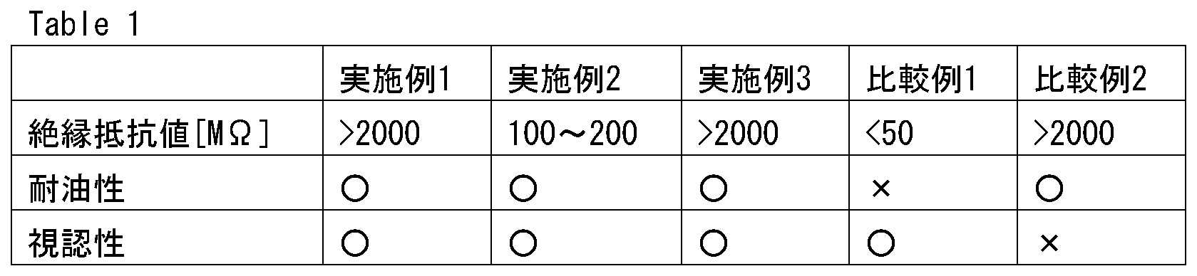
絶縁抵抗値が50MΩを超えるものを「○」とし、絶縁抵抗値が50MΩ以下であるものを「×」とする二段階の評価を行なった。
なお、絶縁抵抗値の測定には、メグオームハイテスタ3453(日置電機株式会社社製)を用いた。
[動作表示部の視認性評価]
目視にて動作表示の視認性を判定した。例えば、図17に示す通り、フラットタイプの光電センサでは、2mの距離をあけて、上部[図17(a)]、光学面正対[図17(b)]、光学面裏面[図17(c)]、光学面正対斜め上[図17(d)]、光学面裏面斜め上[図17(e)]の5方向から動作表示の視認性を確認した。全方向から、視認確認が出来れば「○」と判定し、一方向でも視認確認が出来なければ「×」と判定した。
目視にて動作表示の視認性を判定した。例えば、図17に示す通り、フラットタイプの光電センサでは、2mの距離をあけて、上部[図17(a)]、光学面正対[図17(b)]、光学面裏面[図17(c)]、光学面正対斜め上[図17(d)]、光学面裏面斜め上[図17(e)]の5方向から動作表示の視認性を確認した。全方向から、視認確認が出来れば「○」と判定し、一方向でも視認確認が出来なければ「×」と判定した。
[実施例1]
結晶性を有する熱可塑性ホットメルト樹脂としてポリエステル系樹脂a1(結晶化度:12%)を用いて、光電センサ用基板モジュールを成形した。成形機は、キヤノン電子製成形機LS-300iを使用した。組立中間品を金型にインサートして、以下の成形条件で成型封止を行い、光電センサ用基板モジュールを得た。成形条件は、樹脂温度240℃、成形圧力10MPa、金型温度50℃、冷却時間60secとした。前記の光電センサ用基板モジュールに筐体およびウィンドウを取り付け、光電センサの完成品を得た。前記光電センサを用いて、耐油性試験、および視認性試験を行った。結果を表1に示す。
結晶性を有する熱可塑性ホットメルト樹脂としてポリエステル系樹脂a1(結晶化度:12%)を用いて、光電センサ用基板モジュールを成形した。成形機は、キヤノン電子製成形機LS-300iを使用した。組立中間品を金型にインサートして、以下の成形条件で成型封止を行い、光電センサ用基板モジュールを得た。成形条件は、樹脂温度240℃、成形圧力10MPa、金型温度50℃、冷却時間60secとした。前記の光電センサ用基板モジュールに筐体およびウィンドウを取り付け、光電センサの完成品を得た。前記光電センサを用いて、耐油性試験、および視認性試験を行った。結果を表1に示す。
[実施例2]
実施例1においてポリエステル系樹脂a1を用いたことに代えてポリエステル系樹脂a2(結晶化度:8%)を用いたこと以外は、実施例1と同様にして実施例2の光電センサ完成品を得た。耐油性試験および視認性試験の結果を表1に示す。
実施例1においてポリエステル系樹脂a1を用いたことに代えてポリエステル系樹脂a2(結晶化度:8%)を用いたこと以外は、実施例1と同様にして実施例2の光電センサ完成品を得た。耐油性試験および視認性試験の結果を表1に示す。
[実施例3]
実施例1においてポリエステル系樹脂a1を用いたことに代えてポリエステル系樹脂a3(結晶化度:22%)を用いたこと以外は、実施例1と同様にして実施例3の光電センサ完成品を得た。耐油性試験および視認性試験の結果を表1に示す。
実施例1においてポリエステル系樹脂a1を用いたことに代えてポリエステル系樹脂a3(結晶化度:22%)を用いたこと以外は、実施例1と同様にして実施例3の光電センサ完成品を得た。耐油性試験および視認性試験の結果を表1に示す。
[比較例1]
実施例1においてポリエステル系樹脂a1を用いたことに代えてポリエステル系樹脂b1(結晶化度:6%)を用いたこと以外は、実施例1と同様にして比較例1の光電センサ完成品を得た。耐油性試験および視認性試験の結果を表1に示す。
実施例1においてポリエステル系樹脂a1を用いたことに代えてポリエステル系樹脂b1(結晶化度:6%)を用いたこと以外は、実施例1と同様にして比較例1の光電センサ完成品を得た。耐油性試験および視認性試験の結果を表1に示す。
[比較例2]
実施例1においてポリエステル系樹脂a1を用いたことに代えてポリエステル系樹脂b2(結晶化度:25%)を用いたこと以外は、実施例1と同様にして比較例2の光電センサ完成品を得た。耐油性試験および視認性試験の結果を表1に示す。
実施例1においてポリエステル系樹脂a1を用いたことに代えてポリエステル系樹脂b2(結晶化度:25%)を用いたこと以外は、実施例1と同様にして比較例2の光電センサ完成品を得た。耐油性試験および視認性試験の結果を表1に示す。
<付記>
以上のように、上記の実施の形態よび変形例は以下のような開示を含む。
以上のように、上記の実施の形態よび変形例は以下のような開示を含む。
[構成1]
基板(13)、ならびに、前記基板(13)に実装された動作表示部(11)および投受光素子(12)を含む実装基板(10)と、
前記実装基板(10)の一部を被覆する被覆部材(1)と、
を含む基板モジュール(100,200,300,400)であって、
前記被覆部材(1)は、前記動作表示部(11)を被覆し、かつ、前記投受光素子(12)が前記被覆部材(1)から露出するように形成されており、
前記被覆部材(1)は、結晶性を有する熱可塑性ホットメルト樹脂から形成され、X線回折法で計測される結晶化度が8%以上、22%以下である、光電センサ用基板モジュール。
基板(13)、ならびに、前記基板(13)に実装された動作表示部(11)および投受光素子(12)を含む実装基板(10)と、
前記実装基板(10)の一部を被覆する被覆部材(1)と、
を含む基板モジュール(100,200,300,400)であって、
前記被覆部材(1)は、前記動作表示部(11)を被覆し、かつ、前記投受光素子(12)が前記被覆部材(1)から露出するように形成されており、
前記被覆部材(1)は、結晶性を有する熱可塑性ホットメルト樹脂から形成され、X線回折法で計測される結晶化度が8%以上、22%以下である、光電センサ用基板モジュール。
[構成2]
前記投受光素子(12)と対面する位置に設置されるカバー部(25)をさらに含み、
前記カバー部(25)は、少なくとも一部が被覆部材(1)から露出している、構成1に記載の光電センサ用基板モジュール。
前記投受光素子(12)と対面する位置に設置されるカバー部(25)をさらに含み、
前記カバー部(25)は、少なくとも一部が被覆部材(1)から露出している、構成1に記載の光電センサ用基板モジュール。
[構成3]
前記結晶性を有する熱可塑性ホットメルト樹脂はポリエステル系樹脂である、構成1または構成2に記載の光電センサ用基板モジュール。
前記結晶性を有する熱可塑性ホットメルト樹脂はポリエステル系樹脂である、構成1または構成2に記載の光電センサ用基板モジュール。
[構成4]
前記実装基板(10)は、前記基板(13)に実装された電子部品(24)をさらに含む、構成1~構成3のいずれかに記載の光電センサ用基板モジュール。
前記実装基板(10)は、前記基板(13)に実装された電子部品(24)をさらに含む、構成1~構成3のいずれかに記載の光電センサ用基板モジュール。
[構成5]
外部接続部材(14)をさらに備える、構成1~構成4のいずれかに記載の光電センサ用基板モジュール。
外部接続部材(14)をさらに備える、構成1~構成4のいずれかに記載の光電センサ用基板モジュール。
[構成6]
構成1~構成5のいずれかに記載の光電センサ用基板モジュールと、筐体(50)と、ウインドウ(51)とを備える光電センサ(500,600)。
構成1~構成5のいずれかに記載の光電センサ用基板モジュールと、筐体(50)と、ウインドウ(51)とを備える光電センサ(500,600)。
今回開示された実施形態はすべての点で例示であって制限的なものではないと考えられるべきである。本発明の範囲は上記した実施の形態および実施例ではなく請求の範囲によって示され、請求の範囲と均等の意味および範囲内でのすべての変更が含まれることが意図される。
1 封止部材、10 実装基板、11 動作表示部、12 投受光素子、13 基板、14 外部接続部材、15 プロテクタ、16 底面、17,18 側面、19 上面、20 前面、21 背面、22 投光部、23 受光部、24 電子部品、25 カバー部、26 ホルダ、27 カバー、50 筐体、50a 第1部材、50b 第2部材、51 ウインドウ、100,200,300,400 光電センサ用基板モジュール、500,600 光電センサ。
Claims (6)
- 基板、ならびに、前記基板に実装された動作表示部および投受光素子を含む実装基板と、
前記実装基板の一部を被覆する被覆部材と、
を含む基板モジュールであって、
前記被覆部材は、前記動作表示部を被覆し、かつ、前記投受光素子が前記被覆部材から露出するように形成されており、
前記被覆部材は、結晶性を有する熱可塑性ホットメルト樹脂から形成され、X線回折法で計測される結晶化度が8%以上、22%以下である、光電センサ用基板モジュール。 - 前記投受光素子と対面する位置に設置されるカバー部をさらに含み、
前記カバー部は、少なくとも一部が被覆部材から露出している、請求項1に記載の光電センサ用基板モジュール。 - 前記結晶性を有する熱可塑性ホットメルト樹脂はポリエステル系樹脂である、請求項1または2に記載の光電センサ用基板モジュール。
- 前記実装基板は、前記基板に実装された電子部品をさらに含む、請求項1~3のいずれか一項に記載の光電センサ用基板モジュール。
- 外部接続部材をさらに備える、請求項1~4のいずれか一項に記載の光電センサ用基板モジュール。
- 請求項1~5のいずれか一項に記載の光電センサ用基板モジュールと、筐体と、ウインドウとを備える光電センサ。
Applications Claiming Priority (2)
| Application Number | Priority Date | Filing Date | Title |
|---|---|---|---|
| JP2019-047169 | 2019-03-14 | ||
| JP2019047169A JP7047801B2 (ja) | 2019-03-14 | 2019-03-14 | 光電センサ用基板モジュールおよび光電センサ |
Publications (1)
| Publication Number | Publication Date |
|---|---|
| WO2020184104A1 true WO2020184104A1 (ja) | 2020-09-17 |
Family
ID=72427953
Family Applications (1)
| Application Number | Title | Priority Date | Filing Date |
|---|---|---|---|
| PCT/JP2020/006477 Ceased WO2020184104A1 (ja) | 2019-03-14 | 2020-02-19 | 光電センサ用基板モジュールおよび光電センサ |
Country Status (2)
| Country | Link |
|---|---|
| JP (1) | JP7047801B2 (ja) |
| WO (1) | WO2020184104A1 (ja) |
Citations (2)
| Publication number | Priority date | Publication date | Assignee | Title |
|---|---|---|---|---|
| JP2009079088A (ja) * | 2007-09-25 | 2009-04-16 | Nippon Zeon Co Ltd | ノルボルネン化合物開環ブロック共重合体水素化物、その製造方法および成形体 |
| JP2014032805A (ja) * | 2012-08-02 | 2014-02-20 | Keyence Corp | 光学センサ |
-
2019
- 2019-03-14 JP JP2019047169A patent/JP7047801B2/ja active Active
-
2020
- 2020-02-19 WO PCT/JP2020/006477 patent/WO2020184104A1/ja not_active Ceased
Patent Citations (2)
| Publication number | Priority date | Publication date | Assignee | Title |
|---|---|---|---|---|
| JP2009079088A (ja) * | 2007-09-25 | 2009-04-16 | Nippon Zeon Co Ltd | ノルボルネン化合物開環ブロック共重合体水素化物、その製造方法および成形体 |
| JP2014032805A (ja) * | 2012-08-02 | 2014-02-20 | Keyence Corp | 光学センサ |
Also Published As
| Publication number | Publication date |
|---|---|
| JP7047801B2 (ja) | 2022-04-05 |
| JP2020149890A (ja) | 2020-09-17 |
Similar Documents
| Publication | Publication Date | Title |
|---|---|---|
| US7048450B2 (en) | Optoelectronic module with transmitter chip and connecting piece for the module with respect to an optical fiber and with respect to a circuit board, and methods for producing the same | |
| WO2008152909A1 (ja) | レーザー透過性樹脂成形品及びその複合成形品 | |
| BRPI1100301A2 (pt) | sensor de proximidade | |
| CN113514840A (zh) | 位移传感器 | |
| JP7047801B2 (ja) | 光電センサ用基板モジュールおよび光電センサ | |
| CN112168091B (zh) | 扫地机器人 | |
| JP5964687B2 (ja) | 光学センサ | |
| CN115298589A (zh) | 光电传输复合模块 | |
| JP6097020B2 (ja) | 光学センサ | |
| KR20170050289A (ko) | 디스플레이 장치 | |
| US7570439B2 (en) | Optical module and optical system | |
| JP2010137590A (ja) | 車両用灯具及びその組付け方法 | |
| KR20240146554A (ko) | 광 전기 복합 전송 모듈 및 그것을 사용한 광 통신 케이블 | |
| JP4840067B2 (ja) | Ledランプ装置 | |
| US7371652B2 (en) | Alignment using fiducial features | |
| JP6820584B6 (ja) | 伝熱体および帯状ledライト | |
| US6704507B2 (en) | Optical range finder | |
| JP7331570B2 (ja) | 電子機器、非接触スイッチ、および光電センサ | |
| US7182526B1 (en) | Modular system of optoelectronic components, and optoelectronic component for use in such a system | |
| JP2013251246A (ja) | 光学センサ | |
| JP2000323860A (ja) | 連装型電子機器ユニット | |
| CN110858053A (zh) | 光电模组、深度撷取装置及电子设备 | |
| JP2014032806A (ja) | 光学センサ | |
| EP3706249A1 (en) | Electrical connector for motor vehicles | |
| JP4905070B2 (ja) | 光パイプ内蔵型lanコネクタ用遮光板の形成方法 |
Legal Events
| Date | Code | Title | Description |
|---|---|---|---|
| 121 | Ep: the epo has been informed by wipo that ep was designated in this application |
Ref document number: 20770280 Country of ref document: EP Kind code of ref document: A1 |
|
| NENP | Non-entry into the national phase |
Ref country code: DE |
|
| 122 | Ep: pct application non-entry in european phase |
Ref document number: 20770280 Country of ref document: EP Kind code of ref document: A1 |