WO2020183808A1 - 固体撮像素子、および、撮像装置 - Google Patents
固体撮像素子、および、撮像装置 Download PDFInfo
- Publication number
- WO2020183808A1 WO2020183808A1 PCT/JP2019/046089 JP2019046089W WO2020183808A1 WO 2020183808 A1 WO2020183808 A1 WO 2020183808A1 JP 2019046089 W JP2019046089 W JP 2019046089W WO 2020183808 A1 WO2020183808 A1 WO 2020183808A1
- Authority
- WO
- WIPO (PCT)
- Prior art keywords
- voltage
- input
- transistor
- gate
- differential transistor
- Prior art date
- Legal status (The legal status is an assumption and is not a legal conclusion. Google has not performed a legal analysis and makes no representation as to the accuracy of the status listed.)
- Ceased
Links
Images







Classifications
-
- H—ELECTRICITY
- H04—ELECTRIC COMMUNICATION TECHNIQUE
- H04N—PICTORIAL COMMUNICATION, e.g. TELEVISION
- H04N25/00—Circuitry of solid-state image sensors [SSIS]; Control thereof
- H04N25/70—SSIS architectures; Circuits associated therewith
- H04N25/76—Addressed sensors, e.g. MOS or CMOS sensors
- H04N25/77—Pixel circuitry, e.g. memories, A/D converters, pixel amplifiers, shared circuits or shared components
- H04N25/772—Pixel circuitry, e.g. memories, A/D converters, pixel amplifiers, shared circuits or shared components comprising A/D, V/T, V/F, I/T or I/F converters
-
- H—ELECTRICITY
- H04—ELECTRIC COMMUNICATION TECHNIQUE
- H04N—PICTORIAL COMMUNICATION, e.g. TELEVISION
- H04N25/00—Circuitry of solid-state image sensors [SSIS]; Control thereof
- H04N25/70—SSIS architectures; Circuits associated therewith
- H04N25/709—Circuitry for control of the power supply
-
- H—ELECTRICITY
- H03—ELECTRONIC CIRCUITRY
- H03F—AMPLIFIERS
- H03F3/00—Amplifiers with only discharge tubes or only semiconductor devices as amplifying elements
- H03F3/34—DC amplifiers in which all stages are DC-coupled
-
- H—ELECTRICITY
- H03—ELECTRONIC CIRCUITRY
- H03K—PULSE TECHNIQUE
- H03K5/00—Manipulating of pulses not covered by one of the other main groups of this subclass
- H03K5/01—Shaping pulses
- H03K5/08—Shaping pulses by limiting; by thresholding; by slicing, i.e. combined limiting and thresholding
-
- H—ELECTRICITY
- H03—ELECTRONIC CIRCUITRY
- H03M—CODING; DECODING; CODE CONVERSION IN GENERAL
- H03M1/00—Analogue/digital conversion; Digital/analogue conversion
- H03M1/12—Analogue/digital converters
- H03M1/50—Analogue/digital converters with intermediate conversion to time interval
- H03M1/56—Input signal compared with linear ramp
-
- H—ELECTRICITY
- H04—ELECTRIC COMMUNICATION TECHNIQUE
- H04N—PICTORIAL COMMUNICATION, e.g. TELEVISION
- H04N25/00—Circuitry of solid-state image sensors [SSIS]; Control thereof
- H04N25/70—SSIS architectures; Circuits associated therewith
- H04N25/76—Addressed sensors, e.g. MOS or CMOS sensors
- H04N25/78—Readout circuits for addressed sensors, e.g. output amplifiers or A/D converters
-
- H—ELECTRICITY
- H04—ELECTRIC COMMUNICATION TECHNIQUE
- H04N—PICTORIAL COMMUNICATION, e.g. TELEVISION
- H04N25/00—Circuitry of solid-state image sensors [SSIS]; Control thereof
- H04N25/70—SSIS architectures; Circuits associated therewith
- H04N25/76—Addressed sensors, e.g. MOS or CMOS sensors
- H04N25/77—Pixel circuitry, e.g. memories, A/D converters, pixel amplifiers, shared circuits or shared components
- H04N25/778—Pixel circuitry, e.g. memories, A/D converters, pixel amplifiers, shared circuits or shared components comprising amplifiers shared between a plurality of pixels, i.e. at least one part of the amplifier must be on the sensor array itself
Definitions
- This technology relates to a solid-state image sensor and an image pickup device. More specifically, the present invention relates to a solid-state image pickup device provided with a single-slope type ADC, and an image pickup device.
- the power supply voltage required for operation is lowered by adding a voltage dividing circuit to reduce power consumption.
- the difference between the reset level of the pixel signal and the signal level is very large, the gate-source voltage of the differential transistor increases, and the parasitic capacitance of the differential transistor may increase due to the increase. There is. Due to this increase in parasitic capacitance, an error occurs in the inversion timing of the comparison result between the reference signal and the pixel signal, and there is a problem that the image quality of the image data deteriorates due to the error.
- This technology was created in view of this situation, and aims to improve the image quality of image data in a solid-state image sensor equipped with a comparator that compares a reference signal and a pixel signal.
- This technology has been made to solve the above-mentioned problems, and the first aspect thereof is a voltage dividing circuit that supplies a voltage dividing voltage between an input input voltage and a predetermined reference voltage, and a gate.
- An input-side differential transistor that outputs a drain current corresponding to the gate-source voltage between the input voltage divider and a predetermined source voltage, and a voltage corresponding to the drain current as the input voltage and the reference voltage.
- It is a solid-state imaging device including an output-side differential transistor that outputs as a result of comparison with the above, and a control transistor that lowers the gate-source voltage when the input voltage is out of a predetermined range. This has the effect of reducing the gate-source voltage of the differential transistor.
- a tail current source commonly connected to the source of the input side differential transistor and the source of the output side differential transistor, and its own drain to the drain of the input side differential transistor.
- the input side current mirror transistor to which the gate is connected, and the output side current mirror transistor in which its own drain is connected to the drain of the output side differential transistor and its own gate is connected to the gate of the input side current mirror transistor.
- the gate of the control transistor may be connected to the output node of the voltage dividing circuit, and the source may be connected to the connection point of the input side differential transistor and the input side current mirror transistor. This has the effect of reducing the gate-source voltage of the differential transistor in the comparator in which the diode-connected transistor is arranged.
- one end is connected to a tail current source commonly connected to the source of the input side differential transistor and the source of the output side differential transistor, and to the drain of the input side differential transistor.
- the input side resistor is further provided with an output side resistor having one end connected to the drain of the output side differential transistor, the gate of the control transistor is connected to the output node of the voltage dividing circuit, and the source is ,
- the input side differential transistor and the input side resistor may be connected to the connection point. This has the effect of reducing the gate-source voltage of the differential transistor in a comparator with only N-type or P-type transistors.
- the input side current mirror transistor in which the connection point of the input side differential transistor and the input side resistor is connected to the gate and the other end of the input side resistor is connected to the drain, and the above.
- An output-side current mirror transistor in which its own drain is connected to the other end of the output-side resistor and its own gate is connected to the gate of the input-side current mirror transistor may be further provided. This has the effect of reducing power consumption.
- the input side differential transistor, the output side differential transistor, and the control transistor are P-type transistors, and the control transistor is used when the input voltage is lower than a predetermined value.
- the drain voltage of the input side differential transistor may be lowered. This has the effect of lowering the gate-source voltage of the differential transistor when a signal level lower than the reset level is input.
- the input side differential transistor, the output side differential transistor, and the control transistor are N-type transistors, and the control transistor is used when the input voltage is higher than a predetermined value.
- the drain voltage of the input side differential transistor may be increased. This has the effect of lowering the gate-source voltage of the differential transistor when a signal level higher than the reset level is input.
- the voltage dividing circuit may change the voltage dividing ratio between the input voltage and the reference voltage according to the control signal. This has the effect of reducing the gate-source voltage of the differential transistor in a comparator with a variable voltage division ratio.
- a second aspect of the present technology is a voltage divider circuit that supplies a voltage divider between the input input voltage and a predetermined reference voltage, and between the voltage divider input to the gate and the predetermined source voltage.
- An input-side differential transistor that outputs a drain current corresponding to the gate-source voltage
- an output-side differential transistor that outputs a voltage corresponding to the drain current as a result of comparison between the input voltage and the reference voltage, and the above.
- This imaging device includes a control transistor that lowers the gate-source voltage when the input voltage is out of the predetermined range, and a counter that counts the count value based on the comparison result. As a result, the gate-source voltage of the differential transistor is lowered, and the image quality of the image data is improved.
- MOS Metal-Oxide-Semiconductor
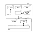
- FIG. 1 is a block diagram showing a configuration example of the image pickup apparatus 100 according to the first embodiment of the present technology.
- the image pickup device 100 is a device for capturing image data, and includes an optical unit 110, a solid-state image sensor 200, and a DSP (Digital Signal Processing) circuit 120. Further, the image pickup apparatus 100 includes a display unit 130, an operation unit 140, a bus 150, a frame memory 160, a storage unit 170, and a power supply unit 180.
- a digital camera such as a digital still camera, a smartphone having an image pickup function, a personal computer, an in-vehicle camera, or the like is assumed.
- the optical unit 110 collects the light from the subject and guides it to the solid-state image sensor 200.
- the solid-state image sensor 200 generates image data by photoelectric conversion in synchronization with the vertical synchronization signal VSYNC.
- the vertical synchronization signal VSYNC is a periodic signal having a predetermined frequency indicating the timing of imaging.
- the solid-state image sensor 200 supplies the generated image data to the DSP circuit 120 via the signal line 209.
- the DSP circuit 120 executes predetermined image processing on the image data from the solid-state image sensor 200.
- the DSP circuit 120 outputs the processed image data to the frame memory 160 or the like via the bus 150.
- the display unit 130 displays image data.
- a liquid crystal panel or an organic EL (Electro Luminescence) panel is assumed.
- the operation unit 140 generates an operation signal according to the operation of the user.
- the bus 150 is a common route for the optical unit 110, the solid-state image sensor 200, the DSP circuit 120, the display unit 130, the operation unit 140, the frame memory 160, the storage unit 170, and the power supply unit 180 to exchange data with each other.
- the frame memory 160 holds image data.
- the storage unit 170 stores various data such as image data.
- the power supply unit 180 supplies power to the solid-state image sensor 200, the DSP circuit 120, the display unit 130, and the like.
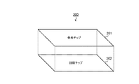
- FIG. 2 is a diagram showing an example of a laminated structure of the solid-state image sensor 200 according to the first embodiment of the present technology.
- the solid-state image sensor 200 includes a circuit chip 202 and a light receiving chip 201 laminated on the circuit chip 202. These chips are electrically connected via a connection such as a via. In addition to vias, it can also be connected by Cu-Cu bonding or bumps.
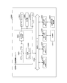
- FIG. 3 is a block diagram showing a configuration example of the solid-state image sensor 200 according to the first embodiment of the present technology.
- the solid-state image sensor 200 includes a row selection unit 211, a DAC (Digital to Analog Converter) 212, and a pixel array unit 213. Further, the solid-state image sensor 200 further includes a timing control unit 214, a constant current source unit 230, an analog-digital conversion unit 300, a horizontal transfer scanning unit 215, and a signal processing unit 216.
- DAC Digital to Analog Converter
- the pixel array unit 213 is arranged on the light receiving chip 201, and other circuits (such as the row selection unit 211) are arranged on the circuit chip 202.
- the circuits arranged in the light receiving chip 201 and the circuit chip 202 are not limited to this configuration.
- the comparator in the analog-digital converter 300 may be arranged on the light receiving chip 201, and the subsequent stage may be arranged on the circuit chip 202.
- a plurality of pixels 220 are arranged in a two-dimensional lattice pattern in the pixel array unit 213.
- the set of pixels 220 arranged in the horizontal direction is referred to as a "row”
- the set of pixels 220 arranged in the direction perpendicular to the row is referred to as a "column”.
- N be the number of these columns (N is an integer).
- a vertical signal line 229 n (n is an integer of 1 to N) is wired in the pixel array unit 213 for each column.
- the pixel 220 generates an analog pixel signal by photoelectric conversion and supplies it to the analog-to-digital conversion unit 300 via the corresponding vertical signal line 229 n .
- the row selection unit 211 selects and drives the rows in order and outputs a pixel signal.
- the DAC 212 generates a predetermined reference signal and supplies it to the analog-to-digital conversion unit 300.
- a reference signal for example, a saw blade-shaped lamp signal is generated.
- the timing control unit 214 controls the operation timings of the row selection unit 211, the analog-digital conversion unit 300, and the horizontal transfer scanning unit 215 in synchronization with the vertical synchronization signal VSYNC.
- a constant current source is arranged in each row in the constant current source unit 230.
- Each constant current source is connected to a corresponding row of vertical signal lines.
- the analog-to-digital conversion unit 300 converts the pixel signal of the row into a digital signal for each row.
- the analog-to-digital conversion unit 300 outputs a digital signal for each column to the signal processing unit 216.
- the horizontal transfer scanning unit 215 controls the analog-to-digital conversion unit 300 to sequentially output the pixel signals in the line.
- the signal processing unit 216 performs predetermined signal processing such as dark current correction and demosaic processing on the digital signal.
- the signal processing unit 216 supplies image data composed of the processed signal to the DSP circuit 120 via the signal line 209.
- FIG. 4 is a circuit diagram showing a configuration example of the pixel 220 according to the first embodiment of the present technology.
- the pixel 220 includes a photoelectric conversion element 221, a transfer transistor 222, a reset transistor 223, a floating diffusion layer 224, an amplification transistor 225, and a selection transistor 226.
- the constant current source unit 230 is provided with a constant current source 231 for each row.
- the constant current source 231 supplies a constant current to the corresponding vertical signal line 229 n .
- the photoelectric conversion element 221 photoelectrically converts incident light to generate an electric charge.
- the transfer transistor 222 transfers an electric charge from the photoelectric conversion element 221 to the floating diffusion layer 224 according to the drive signal TRG from the row selection unit 211.
- the reset transistor 223 is initialized by extracting electric charges from the floating diffusion layer 224 according to the drive signal RST from the row selection unit 211.
- the floating diffusion layer 224 accumulates electric charges and generates a voltage according to the amount of electric charges.
- the amplification transistor 225 amplifies the voltage of the floating diffusion layer 224.
- the selection transistor 226 outputs a signal of the amplified voltage as a pixel signal according to the drive signal SEL from the row selection unit 211.
- the pixel signal is supplied to the analog-to-digital converter 300 via the corresponding vertical signal line 229 n .
- FIG. 5 is a circuit diagram showing a configuration example of the analog-to-digital conversion unit 300 according to the first embodiment of the present technology.
- a plurality of comparators 330, a plurality of counters 310, and a plurality of latches 320 are arranged in the analog-to-digital conversion unit 300. These comparators 330, counters 310 and latches 320 are provided for each row.
- the comparator 330 compares the reference signal RMP with the pixel signal Vin from the corresponding column.
- the comparator 330 supplies the comparison result Vout to the corresponding counter 310.
- the counter 310 counts the count value over a period until the comparison result Vout is inverted according to the control of the timing control unit 214.
- the counter 310 outputs and holds a digital signal indicating the count value to the corresponding latch 320.
- the latch 320 holds the digital signal of the corresponding row.
- the latch 320 outputs a digital signal to the signal processing unit 216 under the control of the horizontal transfer scanning unit 215.
- the analog pixel signal is converted into a digital signal by the above-mentioned comparator 330 and counter 310. That is, the comparator 330 and the counter 310 function as ADCs.
- An ADC having a simple configuration including a comparator and a counter in this way is called a single-slope ADC.
- the analog-to-digital conversion unit 300 also performs CDS (Correlated Double Sampling) processing for obtaining the difference between the reset level and the signal level for each column.
- the reset level is the level of the pixel signal at the time of initialization of the pixel 220
- the signal level is the level of the pixel signal at the end of exposure.
- the CDS processing is realized by the counter 310 performing one of the down count and the up count when converting the reset level, and the counter 310 performing the other of the down count and the up count when converting the signal level. It is also possible to configure the counter 310 to perform only up-counting or only down-counting, and add a circuit for performing CDS processing in the subsequent stage.
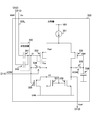
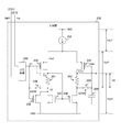
- FIG. 6 is a circuit diagram showing a configuration example of the comparator 330 according to the first embodiment of the present technology.
- the comparator 330 includes a tail current source 331, differential transistors 332 and 333, auto-zero switches 334 and 335, and a control transistor 336. Further, the comparator 330 further includes current mirror transistors 337 and 338, a capacitor 339, and a voltage dividing circuit 340.
- the differential transistor 332 the differential transistor 333, and the control transistor 336
- a pMOS (p-type MOS) transistor is used as the differential transistor 332, the differential transistor 333, and the control transistor 336.
- a pMOS (p-type MOS) transistor is used as the differential transistor 332, the differential transistor 333, and the control transistor 336.
- the current mirror transistors 337 and 338 for example, nMOS (n-type MOS) transistors are used.
- the voltage dividing circuit 340 divides the reference signal RMP and the pixel signal Vin, and supplies the divided pressure.
- the voltage divider circuit 340 includes capacitors 341 and 342.
- the capacitor 341 is inserted between the vertical signal line 229 n for transmitting the pixel signal Vin and the gate of the differential transistor 332, and serves as an input capacitance for the pixel signal Vin.
- the capacitor 342 is inserted between the DAC 212 that supplies the reference signal RMP and the gate of the differential transistor 332, and serves as an input capacitance for the reference signal RMP.
- the voltage of the pixel signal Vin and the reference voltage of the reference signal RMP are divided by the voltage division ratio determined based on the respective capacities of the capacitors 341 and 342.
- the divided voltage between the pixel signal Vin and the reference signal RMP is supplied to the gate of the differential transistor 332 and the control transistor 336 as the gate voltage V1.
- the sources of the differential transistors 332 and 333 are connected to the terminals of the power supply voltage VDD via the tail current source 331. Further, the drain of the differential transistor 332 is connected to the source of the control transistor 336 and the drain of the current mirror transistor 337. On the other hand, the drain of the differential transistor 333 is connected to the drain of the current mirror transistor 338. Further, the voltage of the drain of the differential transistor 333 is output to the counter 310 as a comparison result Vout of the comparator 330.
- the differential transistor 332 is an example of the input-side differential transistor described in the claims.
- the differential transistor 333 is an example of the output-side differential transistor described in the claims.
- the gate and drain of the current mirror transistor 337 are short-circuited. Further, the source of the current mirror transistor 337 is connected to a terminal having a predetermined reference potential (ground potential or the like). On the other hand, the gate of the current mirror transistor 338 is connected to the gate of the current mirror transistor 337, and the source is connected to the terminal of the reference potential. Further, the drain of the control transistor 336 is connected to the terminal of the reference potential.
- the current mirror transistor 337 is an example of the input-side current mirror transistor described in the claims.
- the current mirror transistor 338 is an example of the output side current mirror transistor described in the claims.
- the auto zero switch 334 short-circuits between the gate and drain of the differential transistor 332 according to the control signal AZSW from the timing control unit 214.
- the auto zero switch 335 short-circuits the gate and drain of the differential transistor 333 according to the control signal AZSW from the timing control unit 214.
- the capacitor 339 is inserted between the gate of the differential transistor 333 and the terminal of the reference potential, and a constant voltage VSH is applied to the gate of the differential transistor 333.
- the timing control unit 214 controls the auto zero switch 334 in the closed state at the timing immediately before each of the reset level conversion period and the signal level conversion period, and performs the auto zero operation.
- the current mirror transistors 337 and 338 form a current mirror circuit. Further, the circuit including the current mirror circuit, the tail current source 331, and the differential transistors 332 and 333 constitutes a differential amplifier circuit.
- the differential transistor 332 supplies a drain current corresponding to the gate-source voltage between the gate voltage V1 and the source voltage Vtile. Further, from the drain of the differential transistor 333, a voltage corresponding to the drain current is output as a comparison result Vout of the reference signal RMP and the pixel signal Vin.
- the on-resistance of the control transistor 336 is smaller than the on-resistance of the current mirror transistor 337 connected by a diode. Therefore, when the control transistor 336 shifts to the ON state, the drain voltage V2 of the differential transistor 332 drops. As the drain voltage V2 decreases, the source voltage Vtile of the differential transistor 332 also decreases. Due to this decrease in the source voltage Vtile, the gate-source voltage of the differential transistor 332 is decreased.
- FIG. 7 is a diagram for explaining the cause of streaking in the comparative example.
- the pixel 220 stores electrons as an electric charge
- the higher the illuminance of the incident light the lower the signal level of the pixel signal Vin with respect to the reset level.
- the higher the illuminance the greater the amplitude when changing from the reset level to the signal level.
- the amplitude of the pixel signal Vin1 in one column is very large and the amplitude of the pixel signal Vin2 in another column is relatively small.
- the row with the larger amplitude is the aggressor, and the row with the smaller amplitude is the victim.
- the reference signal RMP gradually increases over the AD conversion period.
- the reference signal RMP is the minimum (that is, at the start of AD conversion)
- the gate voltage V1 becomes lower as the amplitude becomes larger
- the gate-source voltage of the differential transistor 332 becomes larger as the gate voltage V1 becomes lower. That is, the larger the amplitude, the larger the gate-source voltage of the differential transistor 332.
- the differential transistor 332 behaves almost like a source follower. In other words, if the gate voltage V1 changes in that state, the drain voltage V2 hardly changes, while the source voltage Vtile is substantially linked to the gate voltage V1. Since the source voltage Vtile is substantially linked to the gate voltage V1, charging / discharging of the parasitic capacitance between the gate and the source of the differential transistor 332 does not occur. Therefore, the effective capacitance of the differential transistor 332 as seen from the DAC 212 can be considered as the parasitic capacitance between the gate and drain of the differential transistor 332.
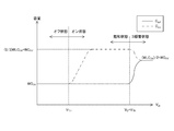
- FIG. 8 is a graph showing an example of the characteristics of the MOS transistor according to the first embodiment of the present technology.
- the vertical axis is the capacitance
- the horizontal axis is the gate-source voltage Vgs .
- the solid line in the figure shows the characteristics of the parasitic capacitance C gd between the gate and drain of the MOS transistor
- the alternate long and short dash line shows the characteristics of the parasitic capacitance C gs between the gate and source of the MOS transistor.
- the MOS transistor When the gate-source voltage V gs exceeds the threshold voltage V TH of the MOS transistor, the MOS transistor shifts to a state called a saturated state, and the parasitic capacitance C gs increases. As the threshold voltage VTH increases, the parasitic capacitance Cgs saturates. Then, when the gate-source voltage V gs exceeds the sum of the drain voltage V D and the threshold voltage V TH , the MOS transistor shifts to a state called a three-pole state. During the transition to the three-pole state, the parasitic capacitance C gs decreases while the parasitic capacitance C gd increases.
- the effective capacitance of the differential transistor 332 is the parasitic capacitance C gd between the gate and drain of the differential transistor 332. Therefore, the amplitude of the aggressor is very large, and when the differential transistor 332 shifts to the three-pole state, the effective capacitance (parasitic capacitance C gd ) of the differential transistor 332 as seen from the DAC 212 increases.
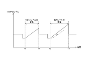
- FIG. 9 is a timing chart showing an example of fluctuation of the reference signal RMP in the comparative example.
- the reference signal RMP gradually increases from the initial value over the conversion period of the reset level of the timings T0 to T1. Further, the signal level is gradually increased from the initial value over the conversion period of the signal levels of the timings T2 to T3.
- the delay in reversal timing due to the increase in parasitic capacitance caused by the aggressor occurs not only in the aggressor but also in the victim. Therefore, for example, in the comparative example, whitening streaking occurs when the illuminance is high.
- the amplitude of the pixel signal may be reduced, but this is not preferable because the dynamic range is lowered.
- the transition to the three-pole state occurs when the amplitude of the pixel signal Vin is approximately Ac -1 ⁇
- V thp is the threshold voltage of the P-type differential transistor 332.
- Ac is a transmission gain (so-called auto-zero gain) from the vertical signal line 229 n to the node of the gate voltage V1.
- the transmission gain Ac is about 0.5. In reality, it is attenuated a little more by other parasitic capacitances, so it is thought that the transmission gain Ac will be reduced to about 0.4 in the case of the above settings.
- control transistor 336 does not operate in the auto-zero state, which determines the characteristics of the comparator 330, and does not affect it, and operates so as to lower the drain voltage V2 only when the amplitude of the pixel signal Vin is large, making it difficult to enter the triode state. is there.
- V dg V gsn- V gs0 + Ac ⁇ ⁇ V VSL ⁇ Ac ⁇ ⁇ V VSL + (2 1/2 -1) ⁇ V ODn0 ⁇ Ac ⁇ ⁇ V VSL +0.4 ⁇ V ODn0 ⁇ ⁇ ⁇ Equation 1
- V gsn the gate-source voltage of the N-type current mirror transistor 337 at the time of signal level input.
- V gs0 is the gate-source voltage of the current mirror transistor 337 at the time of auto zero.
- ⁇ V VSL is the amplitude of the pixel signal Vin.
- V ODn0 is the overdrive voltage (in other words, the pinch-off voltage) of the current mirror transistor 337.
- Equation 2 when the amplitude of the pixel signal Vin is sufficiently large, it is assumed that a current about twice as much as that at the time of auto zero flows through the differential transistor 332. Therefore, when the following equation holds, the differential transistor 332 shifts to the triode state and causes a capacitance change.
- Equation 3 By transforming Equation 2, the following equation is obtained. ⁇ V VSL > Ac -1 ⁇ (
- V sg3 is the source-gate voltage of the control transistor 336.
- V ODp3 is the overdrive voltage of the control transistor 336.
- V thp 3 is the threshold voltage of the control transistor 336.
- Equation 4 in order to prevent the differential transistor 332 from entering the triode state and maintaining the saturated state, the following equation may be satisfied.
- control transistor 336 select an element or transistor size in which ⁇
- the overdrive voltage VODp3 may be made as small as possible by increasing the aspect ratio as much as possible.
- this control transistor 336 is added, its gate capacitance can reduce the auto-zero gain Ac of the comparator 330 and increase the voltage conversion noise of the pixel signal. Therefore, the gate area of the control transistor 336 should be kept sufficiently smaller than that of the differential transistor 332.
- the layout should share the drain and source with the differential transistor 332, for example by equalizing the gate widths, to minimize the increase in parasitic capacitance.
- control transistor 336 Since the control transistor 336 is turned off in the vicinity of the auto zero point, which is the vicinity of the inversion of the comparison result Vout, it can be expected that the control transistor 336 has almost no adverse effect. Further, since ⁇
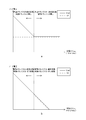
- FIG. 10 is a graph showing an example of the relationship between the amplitude and the node voltage in the first embodiment of the present technology and the comparative example.
- a is a graph showing an example of the relationship between the amplitude and the node voltage in the comparative example without the control transistor 336.
- b is a graph showing an example of the relationship between the amplitude and the node voltage in the first embodiment having the control transistor 336.
- the horizontal axis in the figure shows the amplitude ⁇ V VSL of the pixel signal Vin.
- the amplitude ⁇ V VSL is the difference between the reset level Vinp of the pixel signal Vin and the signal level Vind.
- the vertical axis in the figure shows the node voltage.
- the solid line shows the characteristics of the source voltage Vtile, and the alternate long and short dash line shows the characteristics of the drain voltage V2.
- the source voltage Vtile decreases until it reaches a constant value close to the drain voltage V2.
- the drain voltage V2 is constant.
- the control transistor 336 shifts to the on state when the source voltage Vtile becomes a value close to the drain voltage V2, as illustrated in b in the figure. Then, as the drain current flows on the control transistor 336 side, the source voltage Vtile and the drain voltage V2 decrease as the amplitude ⁇ V VSL increases. Due to this decrease in the source voltage Vtile, the gate-source voltage of the differential transistor 332 is reduced, so that the differential transistor 332 can be maintained in a saturated state. As a result, streaking due to an increase in parasitic capacitance can be suppressed.
- the voltage divider circuit supplies the voltage divider between the input pixel signal Vin voltage and the predetermined reference signal RMP voltage as the gate voltage V1.
- the differential transistor 332 outputs a drain current corresponding to the gate-source voltage between the gate voltage V1 input to the gate and the predetermined source voltage Vtile.
- the differential transistor 333 outputs a voltage corresponding to the drain current from the drain as a comparison result Vout of the pixel signal and the reference signal.
- control transistor 336 lowers the drain voltage V2 when the amplitude ⁇ V VSL is larger than the value when the source voltage Vtile approaches the drain voltage V2 (in other words, when the signal level of the pixel signal is lower than a predetermined value). .. As a result, the gate-source voltage of the differential transistor 332 is reduced, and an increase in parasitic capacitance of the transistor can be suppressed.
- control transistor 336 an nMOS transistor can also be used as described later.
- the control transistor 336 raises the drain voltage V2 and lowers the gate-source voltage of the differential transistor 332.
- control transistor 336 when the pixel signal Vin is out of a predetermined range, the control transistor 336 lowers the gate-source voltage of the differential transistor 332.
- the control transistor 336 lowers the gate-source voltage of the differential transistor 332, so that the differential transistor 332 It is possible to suppress the increase in parasitic capacitance of the transistor. As a result, streaking due to an increase in parasitic capacitance can be prevented and the image quality of the image data can be improved.
- Second Embodiment> in addition to the P-type differential transistor 332 and the like, the N-type current mirror transistor 337 and the like are provided in the comparator 330. However, in such a configuration in which the pMOS transistor and the nMOS transistor are mixed, the manufacturing cost may increase as compared with the case where only one of them is arranged.
- the comparator 330 of the second embodiment is different from the first embodiment in that a resistor is arranged instead of the nMOS transistor.
- FIG. 11 is a circuit diagram showing a configuration example of the comparator 330 according to the second embodiment of the present technology.
- the comparator 330 of this second embodiment differs from the first embodiment in that resistors 351 and 352 are arranged instead of the current mirror transistors 337 and 338.
- resistor 351 One end of the resistor 351 is connected to the drain of the differential transistor 332, and one end of the resistor 352 is connected to the drain of the differential transistor 333.
- the other ends of the resistors 351 and 352 are connected to terminals at a reference potential (such as a ground potential).
- the resistor 351 is an example of the input side resistor described in the claims
- the resistor 352 is an example of the output side resistor described in the claims.
- the transistor in the comparator 330 can be limited to the pMOS transistor. As a result, the number of steps for forming the transistor can be reduced, and the manufacturing cost can be reduced.
- the current mirror transistors 337 and 338 are directly connected to the differential transistors 332 and 333, but in this configuration, the power consumption may not be sufficiently reduced.
- the comparator 330 of the third embodiment is different from the first embodiment in that the minimum operating power supply voltage is lowered by adding a resistor and the power consumption is reduced.
- FIG. 12 is a circuit diagram showing a configuration example of the comparator 330 according to the third embodiment of the present technology.
- the comparator 330 of this third embodiment differs from the first embodiment in that resistors 361 and 362 are further provided.
- resistor 361 is connected to the drain of the differential transistor 332, and the other end is connected to the drain of the current mirror transistor 337.
- One end of the resistor 362 is connected to the drain of the differential transistor 333, and the other end is connected to the drain of the current mirror transistor 338.
- the resistor 361 is an example of the input side resistor described in the claims, and the resistor 362 is an example of the output side resistor described in the claims.
- the gate of the current mirror transistor 337 is connected to the connection point of the resistor 361 and the differential transistor 332.
- the auto zero switch 334 short-circuits the gate of the differential transistor 332 with the connection point of the resistor 361 and the current mirror transistor 337.
- the auto-zero switch 335 short-circuits the gate of the differential transistor 333 with the connection point of the resistor 362 and the current mirror transistor 338.
- control transistor 336 is connected to the connection point of the resistor 361 and the current mirror transistor 337.
- VDD1 VdsT + VgsP + VgsN-VR ⁇ ⁇ ⁇ Equation 6
- VdsT is the drain-source voltage of the tail current source 331 realized by the pMOS transistor.
- VgsP is the gate-source voltage of the P-type differential transistors 332 and 333 during auto-zero operation.
- VgsN is the gate-source voltage of the N-type current mirror transistors 337 and 338.
- VR is the voltage between the terminals of the resistors 361 and 362, respectively.
- VDD1 VdsT + VgsP + VgsN ... Equation 7
- the minimum power supply voltage VDD1 that allows the differential amplifier circuit to operate normally can be lowered.
- the power consumption of the comparator 330 can be reduced.
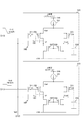
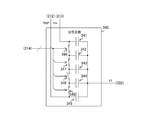
- FIG. 13 is a circuit diagram showing a configuration example of the voltage dividing circuit 340 according to the third embodiment of the present technology.
- the voltage divider circuit 340 of the third embodiment includes capacitors 341 to 345 and switches 346 to 349.
- One end of the capacitors 341 to 345 is commonly connected to the gate of the differential transistor 332.
- the other end of the capacitor 341 is connected to the pixel array unit 213, and the other end of the capacitor 345 is connected to the DAC 212.
- the switch 346 opens and closes the path between the other end of the capacitor 341 and the other end of the capacitor 342 according to the control of the timing control unit 214.
- the switch 347 opens and closes the path between the other end of the capacitor 342 and the other end of the capacitor 343 according to the control of the timing control unit 214.
- the switch 348 opens and closes the path between the other end of the capacitor 343 and the other end of the capacitor 344 according to the control of the timing control unit 214.
- the switch 349 opens and closes the path between the other end of the capacitor 344 and the other end of the capacitor 345 under the control of the timing control unit 214.
- the timing control unit 214 can control each of the switches 346 to 349 to change the ratio of the input capacitance on the vertical signal line side to the input capacitance on the DAC212 side. As a result, the voltage division ratio can be switched as needed.
- the number of capacitors 341 to 345 is not limited to five.
- the number of switches is not limited to four.
- the voltage dividing circuit 340 of the third embodiment can be applied to the second embodiment.
- the resistors 361 and 362 are inserted between the differential transistors 332 and 333 and the current mirror circuit, the minimum necessary amount is equal to the terminal voltage thereof.
- the power supply voltage VDD can be lowered.
- the power consumption of the comparator 330 can be reduced.
- differential amplification is performed by a differential amplifier circuit provided with P-type differential transistors 332 and 333, but in this configuration, the signal level of the pixel signal is higher than the reset level. If this is the case, differential amplification cannot be performed.
- the comparator 330 of the fourth embodiment is different from the first embodiment in that an N-type differential transistor is provided.
- FIG. 14 is a circuit diagram showing a configuration example of the comparator 330 according to the fourth embodiment of the present technology.
- the comparator 330 of this fourth embodiment includes control transistors 371, current mirror transistors 372 and 373, autozero switches 374 and 375, and differential transistors 376 and 377.
- the comparator 330 further includes a tail current source 378, a capacitor 379 and a voltage divider circuit 340.
- nMOS transistor is used as the control transistor 371, the differential transistor 376, and the differential transistor 377. Further, pMOS transistors are used as the current mirror transistors 372 and 373.
- the control transistor 371 and the current mirror transistor 372 are connected in parallel between the terminal of the power supply voltage VDD and the differential transistor 376.
- the current mirror transistor 372 is diode-connected.
- the current mirror transistor 373 and the differential transistor 377 are connected in series between the terminal of the power supply voltage VDD and the tail current source 378.
- the respective sources of the differential transistors 376 and 377 are commonly connected to the tail current source 378.
- the gates of the control transistor 371 and the differential transistor 376 are commonly connected to the voltage dividing circuit 340.
- the capacitor 379 is inserted between the gate of the differential transistor 377 and the terminal of the reference potential.
- the auto zero switch 374 short-circuits between the gate and drain of the differential transistor 376 according to the control of the timing control unit 214.
- the auto zero switch 375 short-circuits between the gate and the drain of the differential transistor 377 under the control of the timing control unit 214.
- the differential transistor 376 is an example of the input-side differential transistor described in the claims.
- the differential transistor 377 is an example of the output-side differential transistor described in the claims.
- the current mirror transistor 372 is an example of the input-side current mirror transistor described in the claims.
- the current mirror transistor 373 is an example of the output-side current mirror transistor described in the claims.
- the signal level is higher than the reset level.
- the gate-source voltage of the differential transistor 376 becomes high.
- the control transistor 371 raises the drain voltage V2 and lowers the gate-source voltage of the differential transistor 376. As a result, an increase in parasitic capacitance of the differential transistor 376 can be suppressed.
- the second embodiment and the third embodiment can also be applied to the comparator 330 of the fourth embodiment.
- the N-type control transistor 371 lowers the gate-source voltage of the differential transistor 376, the signal level becomes higher than the reset level. Even if there is, it is possible to suppress an increase in parasitic capacitance.
- FIG. 15 is a diagram showing an example of a schematic configuration of an endoscopic surgery system 5000 to which the technique according to the present disclosure can be applied.
- FIG. 15 shows a surgeon (doctor) 5067 performing surgery on patient 5071 on patient bed 5069 using the endoscopic surgery system 5000.
- the endoscopic surgery system 5000 includes an endoscope 5001, other surgical tools 5017, a support arm device 5027 for supporting the endoscope 5001, and various devices for endoscopic surgery. It is composed of a cart 5037 equipped with a.
- troccas 5025a to 5025d are punctured into the abdominal wall.
- the lens barrel 5003 of the endoscope 5001 and other surgical tools 5017 are inserted into the body cavity of the patient 5071.
- other surgical tools 5017 a pneumoperitoneum tube 5019, an energy treatment tool 5021 and forceps 5023 are inserted into the body cavity of patient 5071.
- the energy treatment tool 5021 is a treatment tool that cuts and peels tissue, seals a blood vessel, or the like by using a high-frequency current or ultrasonic vibration.
- the surgical tool 5017 shown in the figure is only an example, and as the surgical tool 5017, various surgical tools generally used in endoscopic surgery such as a sword and a retractor may be used.
- the image of the surgical site in the body cavity of the patient 5071 taken by the endoscope 5001 is displayed on the display device 5041.
- the surgeon 5067 performs a procedure such as excising the affected area by using the energy treatment tool 5021 or the forceps 5023 while viewing the image of the surgical site displayed on the display device 5041 in real time.
- the pneumoperitoneum tube 5019, the energy treatment tool 5021, and the forceps 5023 are supported by the operator 5067, an assistant, or the like during the operation.
- the support arm device 5027 includes an arm portion 5031 extending from the base portion 5029.
- the arm portion 5031 is composed of joint portions 5033a, 5033b, 5033c, and links 5035a, 5035b, and is driven by control from the arm control device 5045.
- the endoscope 5001 is supported by the arm portion 5031, and its position and posture are controlled. As a result, the stable position of the endoscope 5001 can be fixed.
- the endoscope 5001 is composed of a lens barrel 5003 in which a region having a predetermined length from the tip is inserted into the body cavity of the patient 5071, and a camera head 5005 connected to the base end of the lens barrel 5003.
- the endoscope 5001 configured as a so-called rigid mirror having a rigid barrel 5003 is illustrated, but the endoscope 5001 is configured as a so-called flexible mirror having a flexible barrel 5003. May be good.
- the tip of the lens barrel 5003 is provided with an opening in which the objective lens is fitted.
- a light source device 5043 is connected to the endoscope 5001, and the light generated by the light source device 5043 is guided to the tip of the lens barrel by a light guide extending inside the lens barrel 5003, and is an objective. It is irradiated toward the observation target in the body cavity of the patient 5071 through the lens.
- the endoscope 5001 may be a direct endoscope, a perspective mirror, or a side endoscope.
- An optical system and an image sensor are provided inside the camera head 5005, and the reflected light (observation light) from the observation target is focused on the image sensor by the optical system.
- the observation light is photoelectrically converted by the image sensor, and an electric signal corresponding to the observation light, that is, an image signal corresponding to the observation image is generated.
- the image signal is transmitted as RAW data to the camera control unit (CCU: Camera Control Unit) 5039.
- the camera head 5005 is equipped with a function of adjusting the magnification and the focal length by appropriately driving the optical system thereof.
- the camera head 5005 may be provided with a plurality of image pickup elements.
- a plurality of relay optical systems are provided inside the lens barrel 5003 in order to guide the observation light to each of the plurality of image pickup elements.
- the CCU 5039 is composed of a CPU (Central Processing Unit), a GPU (Graphics Processing Unit), and the like, and comprehensively controls the operations of the endoscope 5001 and the display device 5041. Specifically, the CCU 5039 performs various image processing for displaying an image based on the image signal, such as development processing (demosaic processing), on the image signal received from the camera head 5005. The CCU 5039 provides the image signal subjected to the image processing to the display device 5041. Further, the CCU 5039 transmits a control signal to the camera head 5005 and controls the driving thereof.
- the control signal may include information about imaging conditions such as magnification and focal length.
- the display device 5041 displays an image based on the image signal processed by the CCU 5039 under the control of the CCU 5039.
- the endoscope 5001 is compatible with high-resolution shooting such as 4K (3840 horizontal pixels x 2160 vertical pixels) or 8K (7680 horizontal pixels x 4320 vertical pixels), and / or 3D display.
- the display device 5041 a device capable of displaying a high resolution and / or a device capable of displaying in 3D can be used corresponding to each of the above.
- a more immersive feeling can be obtained by using a display device 5041 having a size of 55 inches or more.
- a plurality of display devices 5041 having different resolutions and sizes may be provided depending on the application.
- the light source device 5043 is composed of, for example, a light source such as an LED (light LED diode), and supplies irradiation light for photographing the surgical site to the endoscope 5001.
- a light source such as an LED (light LED diode)
- the arm control device 5045 is configured by a processor such as a CPU, and operates according to a predetermined program to control the drive of the arm portion 5031 of the support arm device 5027 according to a predetermined control method.
- the input device 5047 is an input interface for the endoscopic surgery system 5000.
- the user can input various information and input instructions to the endoscopic surgery system 5000 via the input device 5047.
- the user inputs various information related to the surgery, such as physical information of the patient and information about the surgical procedure, via the input device 5047.
- the user gives an instruction to drive the arm portion 5031 via the input device 5047, or an instruction to change the imaging conditions (type of irradiation light, magnification, focal length, etc.) by the endoscope 5001.
- An instruction to drive the energy treatment tool 5021 and the like are input.
- the type of input device 5047 is not limited, and the input device 5047 may be various known input devices.
- the input device 5047 for example, a mouse, a keyboard, a touch panel, a switch, a foot switch 5057 and / or a lever and the like can be applied.
- the touch panel may be provided on the display surface of the display device 5041.
- the input device 5047 is a device worn by the user, such as a glasses-type wearable device or an HMD (Head Mounted Display), and various inputs are made according to the user's gesture and line of sight detected by these devices. Is done. Further, the input device 5047 includes a camera capable of detecting the movement of the user, and various inputs are performed according to the gesture and the line of sight of the user detected from the image captured by the camera. Further, the input device 5047 includes a microphone capable of picking up the user's voice, and various inputs are performed by voice through the microphone.
- a glasses-type wearable device or an HMD Head Mounted Display
- the input device 5047 By configuring the input device 5047 to be able to input various information in a non-contact manner in this way, a user belonging to a clean area (for example, an operator 5067) can operate a device belonging to a dirty area in a non-contact manner. Is possible. In addition, since the user can operate the device without taking his / her hand off the surgical tool that he / she has, the convenience of the user is improved.
- the treatment tool control device 5049 controls the drive of the energy treatment tool 5021 for cauterizing, incising, sealing blood vessels, and the like of tissues.
- the pneumoperitoneum device 5051 gas in the body cavity through the pneumoperitoneum tube 5019 in order to inflate the body cavity of the patient 5071 for the purpose of securing the field of view by the endoscope 5001 and securing the work space of the operator.
- Recorder 5053 is a device capable of recording various information related to surgery.
- the printer 5055 is a device capable of printing various information related to surgery in various formats such as text, images, and graphs.
- the support arm device 5027 includes a base portion 5029, which is a base, and an arm portion 5031 extending from the base portion 5029.
- the arm portion 5031 is composed of a plurality of joint portions 5033a, 5033b, 5033c and a plurality of links 5035a, 5035b connected by the joint portions 5033b, but in FIG. 15, for simplicity.
- the configuration of the arm portion 5031 is shown in a simplified manner. Actually, the shapes, numbers and arrangements of the joint portions 5033a to 5033c and the links 5035a and 5035b, and the direction of the rotation axis of the joint portions 5033a to 5033c are appropriately set so that the arm portion 5031 has a desired degree of freedom. obtain.
- the arm portion 5031 can be preferably configured to have at least 6 degrees of freedom.
- the endoscope 5001 can be freely moved within the movable range of the arm portion 5031, so that the lens barrel 5003 of the endoscope 5001 can be inserted into the body cavity of the patient 5071 from a desired direction. It will be possible.
- Actuators are provided in the joint portions 5033a to 5033c, and the joint portions 5033a to 5033c are configured to be rotatable around a predetermined rotation axis by driving the actuator.
- the arm control device 5045 By controlling the drive of the actuator by the arm control device 5045, the rotation angles of the joint portions 5033a to 5033c are controlled, and the drive of the arm portion 5031 is controlled. Thereby, control of the position and orientation of the endoscope 5001 can be realized.
- the arm control device 5045 can control the drive of the arm unit 5031 by various known control methods such as force control or position control.
- the arm control device 5045 appropriately controls the drive of the arm unit 5031 in response to the operation input.
- the position and orientation of the endoscope 5001 may be controlled.
- the endoscope 5001 at the tip of the arm portion 5031 can be moved from an arbitrary position to an arbitrary position, and then fixedly supported at the moved position.
- the arm portion 5031 may be operated by a so-called master slave method. In this case, the arm portion 5031 can be remotely controlled by the user via an input device 5047 installed at a location away from the operating room.
- the arm control device 5045 When force control is applied, the arm control device 5045 receives an external force from the user and moves the actuators of the joint portions 5033a to 5033c smoothly so that the arm portion 5031 moves smoothly according to the external force. So-called power assist control for driving may be performed.
- the arm portion 5031 when the user moves the arm portion 5031 while directly touching the arm portion 5031, the arm portion 5031 can be moved with a relatively light force. Therefore, the endoscope 5001 can be moved more intuitively and with a simpler operation, and the convenience of the user can be improved.
- the endoscope 5001 was supported by a doctor called a scopist.
- the position of the endoscope 5001 can be fixed more reliably without human intervention, so that an image of the surgical site can be stably obtained. , It becomes possible to perform surgery smoothly.
- the arm control device 5045 does not necessarily have to be provided on the cart 5037. Further, the arm control device 5045 does not necessarily have to be one device. For example, the arm control device 5045 may be provided at each joint portion 5033a to 5033c of the arm portion 5031 of the support arm device 5027, and a plurality of arm control devices 5045 cooperate with each other to drive the arm portion 5031. Control may be realized.
- the light source device 5043 supplies the endoscope 5001 with the irradiation light for photographing the surgical site.
- the light source device 5043 is composed of, for example, an LED, a laser light source, or a white light source composed of a combination thereof.
- a white light source is configured by combining RGB laser light sources, the output intensity and output timing of each color (each wavelength) can be controlled with high accuracy, so that the white balance of the captured image is achieved by the light source device 5043. Can be adjusted.
- the laser light from each of the RGB laser light sources is irradiated to the observation target in a time-division manner, and the drive of the image sensor of the camera head 5005 is controlled in synchronization with the irradiation timing to support each of RGB. It is also possible to capture the image in a time-division manner. According to this method, a color image can be obtained without providing a color filter on the image sensor.
- the drive of the light source device 5043 may be controlled so as to change the intensity of the output light at predetermined time intervals.
- the drive of the image sensor of the camera head 5005 in synchronization with the timing of changing the light intensity to acquire an image in a time-division manner and synthesizing the image, so-called high dynamic without blackout and overexposure Range images can be generated.
- the light source device 5043 may be configured to be able to supply light in a predetermined wavelength band corresponding to special light observation.
- the special light observation for example, by utilizing the wavelength dependence of the absorption of light in body tissues, the mucosal surface layer is irradiated by irradiating a narrow band of light as compared with the irradiation light (that is, white light) during normal observation.
- a so-called narrow band imaging is performed to capture a specific tissue such as blood vessels with high contrast.
- fluorescence observation in which an image is obtained by the fluorescence generated by irradiating the excitation light may be performed.
- the body tissue is irradiated with excitation light to observe the fluorescence from the body tissue (autofluorescence observation), or a reagent such as indocyanine green (ICG) is locally injected into the body tissue and the body tissue is injected.
- An excitation light corresponding to the fluorescence wavelength of the reagent may be irradiated to obtain a fluorescence image.
- the light source device 5043 may be configured to be capable of supplying narrow band light and / or excitation light corresponding to such special light observation.
- FIG. 16 is a block diagram showing an example of the functional configuration of the camera head 5005 and CCU5039 shown in FIG.
- the camera head 5005 has a lens unit 5007, an imaging unit 5009, a driving unit 5011, a communication unit 5013, and a camera head control unit 5015 as its functions.
- the CCU 5039 has a communication unit 5059, an image processing unit 5061, and a control unit 5063 as its functions.
- the camera head 5005 and the CCU 5039 are bidirectionally communicatively connected by a transmission cable 5065.
- the lens unit 5007 is an optical system provided at a connection portion with the lens barrel 5003.
- the observation light taken in from the tip of the lens barrel 5003 is guided to the camera head 5005 and incident on the lens unit 5007.
- the lens unit 5007 is configured by combining a plurality of lenses including a zoom lens and a focus lens.
- the optical characteristics of the lens unit 5007 are adjusted so as to collect the observation light on the light receiving surface of the image sensor of the image pickup unit 5009.
- the zoom lens and the focus lens are configured so that their positions on the optical axis can be moved in order to adjust the magnification and the focus of the captured image.
- the image pickup unit 5009 is composed of an image pickup element and is arranged after the lens unit 5007.
- the observation light that has passed through the lens unit 5007 is focused on the light receiving surface of the image pickup device, and an image signal corresponding to the observation image is generated by photoelectric conversion.
- the image signal generated by the imaging unit 5009 is provided to the communication unit 5013.
- CMOS Complementary Metal Oxide Semiconductor
- the image pickup device for example, an image pickup device that can be used to capture a high-resolution image of 4K or higher may be used.
- the image pickup elements constituting the image pickup unit 5009 are configured to have a pair of image pickup elements for acquiring image signals for the right eye and the left eye corresponding to 3D display, respectively.
- the 3D display enables the operator 5067 to more accurately grasp the depth of the biological tissue in the surgical site.
- the image pickup unit 5009 is composed of a multi-plate type, a plurality of lens units 5007 are also provided corresponding to each image pickup element.
- the imaging unit 5009 does not necessarily have to be provided on the camera head 5005.
- the imaging unit 5009 may be provided inside the lens barrel 5003 immediately after the objective lens.
- the drive unit 5011 is composed of an actuator, and the zoom lens and focus lens of the lens unit 5007 are moved by a predetermined distance along the optical axis under the control of the camera head control unit 5015. As a result, the magnification and focus of the image captured by the imaging unit 5009 can be adjusted as appropriate.
- the communication unit 5013 is composed of a communication device for transmitting and receiving various information to and from the CCU 5039.
- the communication unit 5013 transmits the image signal obtained from the image pickup unit 5009 as RAW data to the CCU 5039 via the transmission cable 5065.
- the image signal is transmitted by optical communication.
- the surgeon 5067 performs the surgery while observing the condition of the affected area with the captured image, so for safer and more reliable surgery, the moving image of the surgical site is displayed in real time as much as possible. This is because it is required.
- the communication unit 5013 is provided with a photoelectric conversion module that converts an electric signal into an optical signal.
- the image signal is converted into an optical signal by the photoelectric conversion module and then transmitted to the CCU 5039 via the transmission cable 5065.
- the communication unit 5013 receives a control signal for controlling the drive of the camera head 5005 from the CCU 5039.
- the control signal includes, for example, information to specify the frame rate of the captured image, information to specify the exposure value at the time of imaging, and / or information to specify the magnification and focus of the captured image. Contains information about the condition.
- the communication unit 5013 provides the received control signal to the camera head control unit 5015.
- the control signal from CCU5039 may also be transmitted by optical communication.
- the communication unit 5013 is provided with a photoelectric conversion module that converts an optical signal into an electric signal, and the control signal is converted into an electric signal by the photoelectric conversion module and then provided to the camera head control unit 5015.
- the above imaging conditions such as frame rate, exposure value, magnification, focus, etc. are automatically set by the control unit 5063 of CCU5039 based on the acquired image signal. That is, the so-called AE (Auto Exposure) function, AF (Auto Focus) function, and AWB (Auto White Balance) function are mounted on the endoscope 5001.
- the camera head control unit 5015 controls the drive of the camera head 5005 based on the control signal from the CCU 5039 received via the communication unit 5013. For example, the camera head control unit 5015 controls the drive of the image sensor of the image pickup unit 5009 based on the information to specify the frame rate of the captured image and / or the information to specify the exposure at the time of imaging. Further, for example, the camera head control unit 5015 appropriately moves the zoom lens and the focus lens of the lens unit 5007 via the drive unit 5011 based on the information that the magnification and the focus of the captured image are specified.
- the camera head control unit 5015 may further have a function of storing information for identifying the lens barrel 5003 and the camera head 5005.
- the camera head 5005 can be made resistant to autoclave sterilization.
- the communication unit 5059 is composed of a communication device for transmitting and receiving various information to and from the camera head 5005.
- the communication unit 5059 receives an image signal transmitted from the camera head 5005 via the transmission cable 5065.
- the image signal can be suitably transmitted by optical communication.
- the communication unit 5059 is provided with a photoelectric conversion module that converts an optical signal into an electric signal.
- the communication unit 5059 provides the image processing unit 5061 with an image signal converted into an electric signal.
- the communication unit 5059 transmits a control signal for controlling the drive of the camera head 5005 to the camera head 5005.
- the control signal may also be transmitted by optical communication.
- the image processing unit 5061 performs various image processing on the image signal which is the RAW data transmitted from the camera head 5005.
- the image processing includes, for example, development processing, high image quality processing (band enhancement processing, super-resolution processing, NR (Noise reduction) processing and / or camera shake correction processing, etc.), and / or enlargement processing (electronic zoom processing). Etc., various known signal processing is included.
- the image processing unit 5061 performs detection processing on the image signal for performing AE, AF, and AWB.
- the image processing unit 5061 is composed of a processor such as a CPU or GPU, and when the processor operates according to a predetermined program, the above-mentioned image processing and detection processing can be performed.
- the image processing unit 5061 is composed of a plurality of GPUs, the image processing unit 5061 appropriately divides the information related to the image signal and performs image processing in parallel by the plurality of GPUs.
- the control unit 5063 performs various controls related to imaging the surgical site with the endoscope 5001 and displaying the captured image. For example, the control unit 5063 generates a control signal for controlling the drive of the camera head 5005. At this time, when the imaging condition is input by the user, the control unit 5063 generates a control signal based on the input by the user. Alternatively, when the endoscope 5001 is equipped with the AE function, the AF function, and the AWB function, the control unit 5063 sets the optimum exposure value, focal length, and the optimum exposure value, depending on the result of the detection process by the image processing unit 5061. The white balance is calculated appropriately and a control signal is generated.
- control unit 5063 causes the display device 5041 to display the image of the surgical unit based on the image signal that has been image-processed by the image processing unit 5061.
- the control unit 5063 recognizes various objects in the surgical site image by using various image recognition techniques.
- the control unit 5063 detects a surgical tool such as forceps, a specific biological part, bleeding, a mist when using the energy treatment tool 5021, etc. by detecting the shape and color of the edge of the object included in the surgical site image. Can be recognized.
- the control unit 5063 uses the recognition result to superimpose and display various surgical support information on the image of the surgical site. By superimposing the surgical support information and presenting it to the surgeon 5067, it becomes possible to proceed with the surgery more safely and surely.
- the transmission cable 5065 that connects the camera head 5005 and the CCU 5039 is an electric signal cable that supports electric signal communication, an optical fiber that supports optical communication, or a composite cable thereof.
- the communication is performed by wire using the transmission cable 5065, but the communication between the camera head 5005 and the CCU 5039 may be performed wirelessly.
- the communication between the two is performed wirelessly, it is not necessary to lay the transmission cable 5065 in the operating room, so that the situation where the movement of the medical staff in the operating room is hindered by the transmission cable 5065 can be solved.
- the example of the endoscopic surgery system 5000 to which the technique according to the present disclosure can be applied has been described above. Although the endoscopic surgery system 5000 has been described here as an example, the system to which the technique according to the present disclosure can be applied is not limited to such an example. For example, the techniques according to the present disclosure may be applied to examination flexible endoscopic systems and microsurgery systems.
- the technique according to the present disclosure can be suitably applied to the imaging unit 5009 among the configurations described above.
- the imaging device 100 of FIG. 1 can be applied to the imaging unit 5009.
- streaking can be suppressed and a clearer surgical site image can be obtained, so that the operation can be performed more safely and reliably.
- the technology according to the present disclosure (this technology) can be applied to various products.
- the technology according to the present disclosure is realized as a device mounted on a moving body of any kind such as an automobile, an electric vehicle, a hybrid electric vehicle, a motorcycle, a bicycle, a personal mobility, an airplane, a drone, a ship, and a robot. May be.
- FIG. 17 is a block diagram showing a schematic configuration example of a vehicle control system, which is an example of a mobile control system to which the technology according to the present disclosure can be applied.
- the vehicle control system 12000 includes a plurality of electronic control units connected via a communication network 12001.
- the vehicle control system 12000 includes a drive system control unit 12010, a body system control unit 12020, an outside information detection unit 12030, an in-vehicle information detection unit 12040, and an integrated control unit 12050.
- a microcomputer 12051, an audio image output unit 12052, and an in-vehicle network I / F (interface) 12053 are shown as a functional configuration of the integrated control unit 12050.
- the drive system control unit 12010 controls the operation of devices related to the drive system of the vehicle according to various programs.
- the drive system control unit 12010 provides a driving force generator for generating the driving force of the vehicle such as an internal combustion engine or a driving motor, a driving force transmission mechanism for transmitting the driving force to the wheels, and a steering angle of the vehicle. It functions as a steering mechanism for adjustment and a control device such as a braking device that generates a braking force of the vehicle.
- the body system control unit 12020 controls the operation of various devices mounted on the vehicle body according to various programs.
- the body system control unit 12020 functions as a keyless entry system, a smart key system, a power window device, or a control device for various lamps such as headlamps, back lamps, brake lamps, blinkers or fog lamps.
- the body system control unit 12020 may be input with radio waves transmitted from a portable device that substitutes for the key or signals of various switches.
- the body system control unit 12020 receives inputs of these radio waves or signals and controls a vehicle door lock device, a power window device, a lamp, and the like.
- the vehicle outside information detection unit 12030 detects information outside the vehicle equipped with the vehicle control system 12000.
- an imaging unit 12031 is connected to the vehicle exterior information detection unit 12030.
- the vehicle outside information detection unit 12030 causes the image pickup unit 12031 to capture an image of the outside of the vehicle and receives the captured image.
- the vehicle exterior information detection unit 12030 may perform object detection processing or distance detection processing such as a person, a vehicle, an obstacle, a sign, or characters on the road surface based on the received image.
- the imaging unit 12031 is an optical sensor that receives light and outputs an electric signal according to the amount of the light received.
- the image pickup unit 12031 can output an electric signal as an image or can output it as distance measurement information.
- the light received by the imaging unit 12031 may be visible light or invisible light such as infrared light.
- the in-vehicle information detection unit 12040 detects the in-vehicle information.
- a driver state detection unit 12041 that detects the driver's state is connected to the in-vehicle information detection unit 12040.
- the driver state detection unit 12041 includes, for example, a camera that images the driver, and the in-vehicle information detection unit 12040 determines the degree of fatigue or concentration of the driver based on the detection information input from the driver state detection unit 12041. It may be calculated, or it may be determined whether the driver is dozing.
- the microcomputer 12051 calculates the control target value of the driving force generator, the steering mechanism, or the braking device based on the information inside and outside the vehicle acquired by the vehicle exterior information detection unit 12030 or the vehicle interior information detection unit 12040, and the drive system control unit.
- a control command can be output to 12010.
- the microcomputer 12051 realizes ADAS (Advanced Driver Assistance System) functions including vehicle collision avoidance or impact mitigation, follow-up driving based on inter-vehicle distance, vehicle speed maintenance driving, vehicle collision warning, vehicle lane deviation warning, and the like. It is possible to perform cooperative control for the purpose of.
- ADAS Advanced Driver Assistance System
- the microcomputer 12051 controls the driving force generator, the steering mechanism, the braking device, and the like based on the information around the vehicle acquired by the vehicle exterior information detection unit 12030 or the vehicle interior information detection unit 12040. It is possible to perform coordinated control for the purpose of automatic driving, etc., which runs autonomously without depending on the operation.
- the microcomputer 12051 can output a control command to the body system control unit 12020 based on the information outside the vehicle acquired by the outside information detection unit 12030.
- the microcomputer 12051 controls the headlamps according to the position of the preceding vehicle or the oncoming vehicle detected by the external information detection unit 12030, and performs cooperative control for the purpose of antiglare such as switching the high beam to the low beam. It can be carried out.
- the audio image output unit 12052 transmits the output signal of at least one of the audio and the image to the output device capable of visually or audibly notifying the passenger or the outside of the vehicle of the information.
- an audio speaker 12061, a display unit 12062, and an instrument panel 12063 are exemplified as output devices.
- the display unit 12062 may include, for example, at least one of an onboard display and a head-up display.
- FIG. 18 is a diagram showing an example of the installation position of the imaging unit 12031.
- the imaging unit 12031 the imaging unit 12101, 12102, 12103, 12104, 12105 is provided.
- the imaging units 12101, 12102, 12103, 12104, 12105 are provided at positions such as the front nose, side mirrors, rear bumpers, back doors, and the upper part of the windshield in the vehicle interior of the vehicle 12100, for example.
- the imaging unit 12101 provided on the front nose and the imaging unit 12105 provided on the upper part of the windshield in the vehicle interior mainly acquire an image in front of the vehicle 12100.
- the imaging units 12102 and 12103 included in the side mirrors mainly acquire images of the side of the vehicle 12100.
- the imaging unit 12104 provided on the rear bumper or the back door mainly acquires an image of the rear of the vehicle 12100.
- the imaging unit 12105 provided on the upper part of the windshield in the vehicle interior is mainly used for detecting a preceding vehicle, a pedestrian, an obstacle, a traffic signal, a traffic sign, a lane, or the like.
- FIG. 18 shows an example of the photographing range of the imaging units 12101 to 12104.
- the imaging range 12111 indicates the imaging range of the imaging unit 12101 provided on the front nose
- the imaging ranges 12112 and 12113 indicate the imaging ranges of the imaging units 12102 and 12103 provided on the side mirrors, respectively
- the imaging range 12114 indicates the imaging range of the imaging units 12102 and 12103.
- the imaging range of the imaging unit 12104 provided on the rear bumper or the back door is shown. For example, by superimposing the image data captured by the imaging units 12101 to 12104, a bird's-eye view image of the vehicle 12100 as viewed from above can be obtained.
- At least one of the image capturing units 12101 to 12104 may have a function of acquiring distance information.
- at least one of the image capturing units 12101 to 12104 may be a stereo camera including a plurality of image capturing elements, or may be an image capturing element having pixels for phase difference detection.
- the microcomputer 12051 has a distance to each three-dimensional object within the imaging range 12111 to 12114 based on the distance information obtained from the imaging units 12101 to 12104, and a temporal change of this distance (relative velocity with respect to the vehicle 12100).
- a predetermined speed for example, 0 km / h or more.
- the microcomputer 12051 can set an inter-vehicle distance to be secured in front of the preceding vehicle in advance, and can perform automatic braking control (including follow-up stop control), automatic acceleration control (including follow-up start control), and the like. In this way, it is possible to perform coordinated control for the purpose of automatic driving or the like in which the vehicle travels autonomously without depending on the operation of the driver.
- the microcomputer 12051 converts three-dimensional object data related to a three-dimensional object into two-wheeled vehicles, ordinary vehicles, large vehicles, pedestrians, electric poles, and other three-dimensional objects based on the distance information obtained from the imaging units 12101 to 12104. It can be classified and extracted and used for automatic avoidance of obstacles. For example, the microcomputer 12051 distinguishes obstacles around the vehicle 12100 into obstacles that can be seen by the driver of the vehicle 12100 and obstacles that are difficult to see. Then, the microcomputer 12051 determines the collision risk indicating the risk of collision with each obstacle, and when the collision risk is equal to or higher than the set value and there is a possibility of collision, the microcomputer 12051 via the audio speaker 12061 or the display unit 12062. By outputting an alarm to the driver and performing forced deceleration and avoidance steering via the drive system control unit 12010, driving support for collision avoidance can be provided.
- At least one of the imaging units 12101 to 12104 may be an infrared camera that detects infrared rays.
- the microcomputer 12051 can recognize a pedestrian by determining whether or not a pedestrian is present in the captured image of the imaging units 12101 to 12104.
- pedestrian recognition includes, for example, a procedure for extracting feature points in an image captured by an imaging unit 12101 to 12104 as an infrared camera, and pattern matching processing for a series of feature points indicating the outline of an object to determine whether or not the pedestrian is a pedestrian. It is done by the procedure to determine.
- the audio image output unit 12052 When the microcomputer 12051 determines that a pedestrian is present in the captured images of the imaging units 12101 to 12104 and recognizes the pedestrian, the audio image output unit 12052 outputs a square contour line for emphasizing the recognized pedestrian.
- the display unit 12062 is controlled so as to superimpose and display. Further, the audio image output unit 12052 may control the display unit 12062 so as to display an icon or the like indicating a pedestrian at a desired position.
- the above is an example of a vehicle control system to which the technology according to the present disclosure can be applied.
- the technique according to the present disclosure can be applied to, for example, the imaging unit 12031 among the configurations described above.
- the imaging device 100 of FIG. 1 can be applied to the imaging unit 12031.
- streaking can be suppressed and a photographed image that is easier to see can be obtained, so that driver fatigue can be reduced.
- the present technology can have the following configurations.
- a voltage divider circuit that supplies a voltage divider between the input input voltage and a predetermined reference voltage, An input-side differential transistor that outputs a drain current according to the gate-source voltage between the partial pressure input to the gate and a predetermined source voltage, and An output-side differential transistor that outputs a voltage corresponding to the drain current as a result of comparison between the input voltage and the reference voltage.
- a solid-state image sensor including a control transistor that lowers the gate-source voltage when the input voltage is out of a predetermined range.
- a tail current source that is commonly connected to the source of the input side differential transistor and the source of the output side differential transistor.
- An input side resistor with one end connected to the drain of the input side differential transistor, An output side resistor having one end connected to the drain of the output side differential transistor is further provided.
- the solid-state image sensor according to (1) wherein the gate of the control transistor is connected to an output node of the voltage dividing circuit, and the source is connected to a connection point of the input-side differential transistor and the input-side resistor.
- the solid-state imaging device further comprising an output-side current mirror transistor in which its own drain is connected to the other end of the output-side resistor and its own gate is connected to the gate of the input-side current mirror transistor. .. (5)
- the input side differential transistor, the output side differential transistor, and the control transistor are P-type transistors.
- the solid-state image sensor according to any one of (1) to (4) above, wherein the control transistor lowers the drain voltage of the input-side differential transistor when the input voltage is lower than a predetermined value.
- the input side differential transistor, the output side differential transistor, and the control transistor are N-type transistors.
- the solid-state image sensor according to any one of (1) to (4) above, wherein the control transistor increases the drain voltage of the input-side differential transistor when the input voltage is higher than a predetermined value.
- the voltage dividing circuit changes the voltage dividing ratio between the input voltage and the reference voltage according to a control signal.
- a voltage divider circuit that supplies a voltage divider between the input input voltage and a predetermined reference voltage, An input-side differential transistor that outputs a drain current according to the gate-source voltage between the partial pressure input to the gate and a predetermined source voltage, and An output-side differential transistor that outputs a voltage corresponding to the drain current as a result of comparison between the input voltage and the reference voltage.
- the control transistor that lowers the gate-source voltage and An imaging device including a counter that counts a count value based on the comparison result.
Landscapes
- Engineering & Computer Science (AREA)
- Multimedia (AREA)
- Signal Processing (AREA)
- Power Engineering (AREA)
- Physics & Mathematics (AREA)
- Nonlinear Science (AREA)
- Theoretical Computer Science (AREA)
- Transforming Light Signals Into Electric Signals (AREA)
- Analogue/Digital Conversion (AREA)
- Manipulation Of Pulses (AREA)
Abstract
Description
1.第1の実施の形態(差動トランジスタのゲート-ソース間電圧を低下させる例)
2.第2の実施の形態(抵抗が接続された差動トランジスタのゲート-ソース間電圧を低下させる例)
3.第3の実施の形態(差動トランジスタのゲート-ソース間電圧を低下させ、カレントミラー回路との間に抵抗を挿入した例)
4.第4の実施の形態(N型の差動トランジスタのゲート-ソース間電圧を低下させる例)
5.内視鏡手術システムへの応用例
6.移動体への応用例
[撮像装置の構成例]
図1は、本技術の第1の実施の形態における撮像装置100の一構成例を示すブロック図である。この撮像装置100は、画像データを撮像するための装置であり、光学部110、固体撮像素子200およびDSP(Digital Signal Processing)回路120を備える。さらに撮像装置100は、表示部130、操作部140、バス150、フレームメモリ160、記憶部170および電源部180を備える。撮像装置100としては、例えば、デジタルスチルカメラなどのデジタルカメラの他、撮像機能を持つスマートフォンやパーソナルコンピュータ、車載カメラ等が想定される。
図2は、本技術の第1の実施の形態における固体撮像素子200の積層構造の一例を示す図である。この固体撮像素子200は、回路チップ202と、その回路チップ202に積層された受光チップ201とを備える。これらのチップは、ビアなどの接続部を介して電気的に接続される。なお、ビアの他、Cu-Cu接合やバンプにより接続することもできる。
図4は、本技術の第1の実施の形態における画素220の一構成例を示す回路図である。この画素220は、光電変換素子221、転送トランジスタ222、リセットトランジスタ223、浮遊拡散層224、増幅トランジスタ225および選択トランジスタ226を備える。
図5は、本技術の第1の実施の形態におけるアナログデジタル変換部300の一構成例を示す回路図である。このアナログデジタル変換部300には、複数の比較器330と、複数のカウンタ310と、複数のラッチ320とが配置される。これらの比較器330、カウンタ310およびラッチ320は、列ごとに設けられる。
図6は、本技術の第1の実施の形態における比較器330の一構成例を示す回路図である。この比較器330は、テール電流源331と、差動トランジスタ332および333と、オートゼロスイッチ334および335と、制御トランジスタ336とを備える。また、比較器330は、カレントミラートランジスタ337および338と、キャパシタ339と、分圧回路340とをさらに備える。差動トランジスタ332、差動トランジスタ333および制御トランジスタ336として、例えば、pMOS(p-type MOS)トランジスタが用いられる。また、カレントミラートランジスタ337および338として、例えば、nMOS(n-type MOS)トランジスタが用いられる。
Vdg=Vgsn-Vgs0+Ac・ΔVVSL
≒Ac・ΔVVSL+(21/2-1)・VODn0
≒Ac・ΔVVSL+0.4×VODn0 ・・・式1
上式において、Vgsnは、信号レベル入力時のN型のカレントミラートランジスタ337のゲート-ソース間電圧である。Vgs0は、オートゼロ時のカレントミラートランジスタ337のゲート-ソース間電圧である。ΔVVSLは、画素信号Vinの振幅である。VODn0は、カレントミラートランジスタ337のオーバードライブ電圧(言い換えれば、ピンチオフ電圧)である。
Ac・ΔVVSL+0.4×VODn0>|Vthp| ・・・式2
ΔVVSL>Ac-1・(|Vthp|-0.4×VODn0) ・・・式3
Vdg≒Vsg3≒VODp3+|Vthp3| ・・・式4
上式において、Vsg3は、制御トランジスタ336のソース-ゲート間電圧である。VODp3は、制御トランジスタ336のオーバードライブ電圧である。Vthp3は、制御トランジスタ336の閾値電圧である。
VODp3+|Vthp3|<|Vthp| ・・・式5
|Vthp|-|Vthp3|-VODp=-Δ|Vthp|-VODp3>0
上述の第1の実施の形態では、比較器330内にP型の差動トランジスタ332等に加えて、N型のカレントミラートランジスタ337等を設けていた。しかし、このようにpMOSトランジスタとnMOSトランジスタとが混在する構成では、いずれか一方のみを配置する場合と比較して、製造コストが増大するおそれがある。この第2の実施の形態の比較器330は、nMOSトランジスタの代わりに、抵抗を配置した点において第1の実施の形態と異なる。
上述の第1の実施の形態では、差動トランジスタ332および333に、カレントミラートランジスタ337および338を直接接続していたが、この構成では、消費電力を十分に低減することができないことがある。この第3の実施の形態の比較器330は、抵抗の追加により、動作可能な最低限の電源電圧を低下させ、消費電力を低減した点において第1の実施の形態と異なる。
VDD1=VdsT+VgsP+VgsN-VR ・・・式6
上式において、VdsTは、テール電流源331をpMOSトランジスタにより実現した際の、そのトランジスタのドレイン-ソース間電圧である。VgsPは、オートゼロ動作の際のP型の差動トランジスタ332および333のゲート-ソース間電圧である。VgsNは、N型のカレントミラートランジスタ337および338のゲート-ソース間電圧である。VRは、抵抗361および362のそれぞれの端子間電圧である。
VDD1=VdsT+VgsP+VgsN ・・・式7
上述の第1の実施の形態では、P型の差動トランジスタ332および333を設けた差動増幅回路により差動増幅を行っていたが、この構成では、画素信号の信号レベルがリセットレベルより高くなる場合に、差動増幅を行うことができない。この第4の実施の形態の比較器330は、N型の差動トランジスタを設けた点において第1の実施の形態と異なる。
本開示に係る技術は、様々な製品へ応用することができる。例えば、本開示に係る技術は、内視鏡手術システムに適用されてもよい。
支持アーム装置5027は、ベース部5029から延伸するアーム部5031を備える。図示する例では、アーム部5031は、関節部5033a、5033b、5033c、及びリンク5035a、5035bから構成されており、アーム制御装置5045からの制御により駆動される。アーム部5031によって内視鏡5001が支持され、その位置及び姿勢が制御される。これにより、内視鏡5001の安定的な位置の固定が実現され得る。
内視鏡5001は、先端から所定の長さの領域が患者5071の体腔内に挿入される鏡筒5003と、鏡筒5003の基端に接続されるカメラヘッド5005と、から構成される。図示する例では、硬性の鏡筒5003を有するいわゆる硬性鏡として構成される内視鏡5001を図示しているが、内視鏡5001は、軟性の鏡筒5003を有するいわゆる軟性鏡として構成されてもよい。
CCU5039は、CPU(Central Processing Unit)やGPU(Graphics Processing Unit)等によって構成され、内視鏡5001及び表示装置5041の動作を統括的に制御する。具体的には、CCU5039は、カメラヘッド5005から受け取った画像信号に対して、例えば現像処理(デモザイク処理)等の、当該画像信号に基づく画像を表示するための各種の画像処理を施す。CCU5039は、当該画像処理を施した画像信号を表示装置5041に提供する。また、CCU5039は、カメラヘッド5005に対して制御信号を送信し、その駆動を制御する。当該制御信号には、倍率や焦点距離等、撮像条件に関する情報が含まれ得る。
支持アーム装置5027は、基台であるベース部5029と、ベース部5029から延伸するアーム部5031と、を備える。図示する例では、アーム部5031は、複数の関節部5033a、5033b、5033cと、関節部5033bによって連結される複数のリンク5035a、5035bと、から構成されているが、図15では、簡単のため、アーム部5031の構成を簡略化して図示している。実際には、アーム部5031が所望の自由度を有するように、関節部5033a~5033c及びリンク5035a、5035bの形状、数及び配置、並びに関節部5033a~5033cの回転軸の方向等が適宜設定され得る。例えば、アーム部5031は、好適に、6自由度以上の自由度を有するように構成され得る。これにより、アーム部5031の可動範囲内において内視鏡5001を自由に移動させることが可能になるため、所望の方向から内視鏡5001の鏡筒5003を患者5071の体腔内に挿入することが可能になる。
光源装置5043は、内視鏡5001に術部を撮影する際の照射光を供給する。光源装置5043は、例えばLED、レーザ光源又はこれらの組み合わせによって構成される白色光源から構成される。このとき、RGBレーザ光源の組み合わせにより白色光源が構成される場合には、各色(各波長)の出力強度及び出力タイミングを高精度に制御することができるため、光源装置5043において撮像画像のホワイトバランスの調整を行うことができる。また、この場合には、RGBレーザ光源それぞれからのレーザ光を時分割で観察対象に照射し、その照射タイミングに同期してカメラヘッド5005の撮像素子の駆動を制御することにより、RGBそれぞれに対応した画像を時分割で撮像することも可能である。当該方法によれば、当該撮像素子にカラーフィルタを設けなくても、カラー画像を得ることができる。
図16を参照して、内視鏡5001のカメラヘッド5005及びCCU5039の機能についてより詳細に説明する。図16は、図15に示すカメラヘッド5005及びCCU5039の機能構成の一例を示すブロック図である。
本開示に係る技術(本技術)は、様々な製品へ応用することができる。例えば、本開示に係る技術は、自動車、電気自動車、ハイブリッド電気自動車、自動二輪車、自転車、パーソナルモビリティ、飛行機、ドローン、船舶、ロボット等のいずれかの種類の移動体に搭載される装置として実現されてもよい。
(1)入力された入力電圧と所定の参照電圧との分圧を供給する分圧回路と、
ゲートに入力された前記分圧と所定のソース電圧との間のゲート-ソース間電圧に応じたドレイン電流を出力する入力側差動トランジスタと、
前記ドレイン電流に応じた電圧を前記入力電圧と前記参照電圧との比較結果として出力する出力側差動トランジスタと、
前記入力電圧が所定範囲外の値である場合には前記ゲート-ソース間電圧を低下させる制御トランジスタと
を具備する固体撮像素子。
(2)前記入力側差動トランジスタのソースと前記出力側差動トランジスタのソースとに共通に接続されたテール電流源と、
前記入力側差動トランジスタのドレインに自身のドレインおよびゲートが接続された入力側カレントミラートランジスタと、
前記出力側差動トランジスタのドレインに自身のドレインが接続され、前記入力側カレントミラートランジスタのゲートに自身のゲートが接続された出力側カレントミラートランジスタと
をさらに具備し、
前記制御トランジスタのゲートは、前記分圧回路の出力ノードに接続され、ソースは、前記入力側差動トランジスタおよび前記入力側カレントミラートランジスタの接続点に接続される
前記(1)記載の固体撮像素子。
(3)前記入力側差動トランジスタのソースと前記出力側差動トランジスタのソースとに共通に接続されたテール電流源と、
前記入力側差動トランジスタのドレインに一端が接続された入力側抵抗と、
前記出力側差動トランジスタのドレインに一端が接続された出力側抵抗と
をさらに具備し、
前記制御トランジスタのゲートは、前記分圧回路の出力ノードに接続され、ソースは、前記入力側差動トランジスタおよび前記入力側抵抗の接続点に接続される
前記(1)記載の固体撮像素子。
(4)前記入力側差動トランジスタおよび前記入力側抵抗の接続点がゲートに接続され、前記入力側抵抗の他端がドレインに接続された入力側カレントミラートランジスタと、
前記出力側抵抗の他端に自身のドレインが接続され、前記入力側カレントミラートランジスタのゲートに自身のゲートが接続された出力側カレントミラートランジスタと
をさらに具備する
前記(3)記載の固体撮像素子。
(5)前記入力側差動トランジスタ、前記出力側差動トランジスタおよび前記制御トランジスタは、P型トランジスタであり、
前記制御トランジスタは、前記入力電圧が所定値より低い場合には前記入力側差動トランジスタのドレイン電圧を低くする
前記(1)から(4)のいずれかに記載の固体撮像素子。
(6)前記入力側差動トランジスタ、前記出力側差動トランジスタおよび前記制御トランジスタは、N型トランジスタであり、
前記制御トランジスタは、前記入力電圧が所定値より高い場合には前記入力側差動トランジスタのドレイン電圧を高くする
前記(1)から(4)のいずれかに記載の固体撮像素子。
(7)前記分圧回路は、制御信号に従って前記入力電圧と前記参照電圧との分圧比を変更する
前記(1)から(6)のいずれかに記載の固体撮像素子。
(8)入力された入力電圧と所定の参照電圧との分圧を供給する分圧回路と、
ゲートに入力された前記分圧と所定のソース電圧との間のゲート-ソース間電圧に応じたドレイン電流を出力する入力側差動トランジスタと、
前記ドレイン電流に応じた電圧を前記入力電圧と前記参照電圧との比較結果として出力する出力側差動トランジスタと、
前記入力電圧が所定範囲外の値である場合には前記ゲート-ソース間電圧を低下させる制御トランジスタと、
前記比較結果に基づいて計数値を計数するカウンタと
を具備する撮像装置。
110 光学部
120 DSP回路
130 表示部
140 操作部
150 バス
160 フレームメモリ
170 記憶部
180 電源部
200 固体撮像素子
201 受光チップ
202 回路チップ
211 行選択部
212 DAC
213 画素アレイ部
214 タイミング制御部
215 水平転送走査部
216 信号処理部
220 画素
221 光電変換素子
222 転送トランジスタ
223 リセットトランジスタ
224 浮遊拡散層
225 増幅トランジスタ
226 選択トランジスタ
230 定電流源部
231 定電流源
300 アナログデジタル変換部
310 カウンタ
320 ラッチ
330 比較器
331、378 テール電流源
332、333、376、377 差動トランジスタ
334、335、374、375 オートゼロスイッチ
336、371 制御トランジスタ
337、338、372.373 カレントミラートランジスタ
339、341~345、379 キャパシタ
340 分圧回路
346~349 スイッチ
351、352、361、362 抵抗
5009、12031 撮像部
Claims (8)
- 入力された入力電圧と所定の参照電圧との分圧を供給する分圧回路と、
ゲートに入力された前記分圧と所定のソース電圧との間のゲート-ソース間電圧に応じたドレイン電流を出力する入力側差動トランジスタと、
前記ドレイン電流に応じた電圧を前記入力電圧と前記参照電圧との比較結果として出力する出力側差動トランジスタと、
前記入力電圧が所定範囲外の値である場合には前記ゲート-ソース間電圧を低下させる制御トランジスタと
を具備する固体撮像素子。 - 前記入力側差動トランジスタのソースと前記出力側差動トランジスタのソースとに共通に接続されたテール電流源と、
前記入力側差動トランジスタのドレインに自身のドレインおよびゲートが接続された入力側カレントミラートランジスタと、
前記出力側差動トランジスタのドレインに自身のドレインが接続され、前記入力側カレントミラートランジスタのゲートに自身のゲートが接続された出力側カレントミラートランジスタと
をさらに具備し、
前記制御トランジスタのゲートは、前記分圧回路の出力ノードに接続され、ソースは、前記入力側差動トランジスタおよび前記入力側カレントミラートランジスタの接続点に接続される
請求項1記載の固体撮像素子。 - 前記入力側差動トランジスタのソースと前記出力側差動トランジスタのソースとに共通に接続されたテール電流源と、
前記入力側差動トランジスタのドレインに一端が接続された入力側抵抗と、
前記出力側差動トランジスタのドレインに一端が接続された出力側抵抗と
をさらに具備し、
前記制御トランジスタのゲートは、前記分圧回路の出力ノードに接続され、ソースは、前記入力側差動トランジスタおよび前記入力側抵抗の接続点に接続される
請求項1記載の固体撮像素子。 - 前記入力側差動トランジスタおよび前記入力側抵抗の接続点がゲートに接続され、前記入力側抵抗の他端がドレインに接続された入力側カレントミラートランジスタと、
前記出力側抵抗の他端に自身のドレインが接続され、前記入力側カレントミラートランジスタのゲートに自身のゲートが接続された出力側カレントミラートランジスタと
をさらに具備する
請求項3記載の固体撮像素子。 - 前記入力側差動トランジスタ、前記出力側差動トランジスタおよび前記制御トランジスタは、P型トランジスタであり、
前記制御トランジスタは、前記入力電圧が所定値より低い場合には前記入力側差動トランジスタのドレイン電圧を低くする
請求項1記載の固体撮像素子。 - 前記入力側差動トランジスタ、前記出力側差動トランジスタおよび前記制御トランジスタは、N型トランジスタであり、
前記制御トランジスタは、前記入力電圧が所定値より高い場合には前記入力側差動トランジスタのドレイン電圧を高くする
請求項1記載の固体撮像素子。 - 前記分圧回路は、制御信号に従って前記入力電圧と前記参照電圧との分圧比を変更する
請求項1記載の固体撮像素子。 - 入力された入力電圧と所定の参照電圧との分圧を供給する分圧回路と、
ゲートに入力された前記分圧と所定のソース電圧との間のゲート-ソース間電圧に応じたドレイン電流を出力する入力側差動トランジスタと、
前記ドレイン電流に応じた電圧を前記入力電圧と前記参照電圧との比較結果として出力する出力側差動トランジスタと、
前記入力電圧が所定範囲外の値である場合には前記ゲート-ソース間電圧を低下させる制御トランジスタと、
前記比較結果に基づいて計数値を計数するカウンタと
を具備する撮像装置。
Priority Applications (4)
| Application Number | Priority Date | Filing Date | Title |
|---|---|---|---|
| US17/436,820 US11653119B2 (en) | 2019-03-14 | 2019-11-26 | Solid-state image sensor and imaging device |
| KR1020217028721A KR102901868B1 (ko) | 2019-03-14 | 2019-11-26 | 고체 촬상 소자, 및 촬상 장치 |
| CN201980091083.0A CN113383495B (zh) | 2019-03-14 | 2019-11-26 | 固态摄像元件和摄像装置 |
| JP2021505507A JP7422133B2 (ja) | 2019-03-14 | 2019-11-26 | 固体撮像素子、および、撮像装置 |
Applications Claiming Priority (2)
| Application Number | Priority Date | Filing Date | Title |
|---|---|---|---|
| JP2019046578 | 2019-03-14 | ||
| JP2019-046578 | 2019-03-14 |
Publications (1)
| Publication Number | Publication Date |
|---|---|
| WO2020183808A1 true WO2020183808A1 (ja) | 2020-09-17 |
Family
ID=72427903
Family Applications (1)
| Application Number | Title | Priority Date | Filing Date |
|---|---|---|---|
| PCT/JP2019/046089 Ceased WO2020183808A1 (ja) | 2019-03-14 | 2019-11-26 | 固体撮像素子、および、撮像装置 |
Country Status (6)
| Country | Link |
|---|---|
| US (1) | US11653119B2 (ja) |
| JP (1) | JP7422133B2 (ja) |
| KR (1) | KR102901868B1 (ja) |
| CN (1) | CN113383495B (ja) |
| TW (1) | TWI837273B (ja) |
| WO (1) | WO2020183808A1 (ja) |
Cited By (1)
| Publication number | Priority date | Publication date | Assignee | Title |
|---|---|---|---|---|
| WO2026023400A1 (ja) * | 2024-07-23 | 2026-01-29 | ソニーセミコンダクタソリューションズ株式会社 | 撮像素子、駆動方法 |
Families Citing this family (6)
| Publication number | Priority date | Publication date | Assignee | Title |
|---|---|---|---|---|
| JP2016012903A (ja) * | 2014-06-02 | 2016-01-21 | ソニー株式会社 | 撮像素子、撮像方法、および電子機器 |
| JP7115493B2 (ja) * | 2017-11-01 | 2022-08-09 | ソニーグループ株式会社 | 手術アームシステム及び手術アーム制御システム |
| WO2020053921A1 (ja) * | 2018-09-10 | 2020-03-19 | オリンパス株式会社 | 半導体装置 |
| JP7659385B2 (ja) * | 2020-12-01 | 2025-04-09 | ソニーセミコンダクタソリューションズ株式会社 | 撮像装置及び電子機器 |
| US12249999B2 (en) | 2023-02-17 | 2025-03-11 | Omnivision Technologies, Inc. | Dual gain column structure for column power area efficiency |
| US12114092B2 (en) * | 2023-02-17 | 2024-10-08 | Omnivision Technologies, Inc. | Dual gain column structure for column power area efficiency |
Citations (4)
| Publication number | Priority date | Publication date | Assignee | Title |
|---|---|---|---|---|
| US20110249162A1 (en) * | 2010-04-13 | 2011-10-13 | Stmicroelectronics (Research & Development) Limited | Analog to digital conversion in image sensors |
| US20170054931A1 (en) * | 2015-08-17 | 2017-02-23 | Omnivision Technologies, Inc. | Readout circuitry to mitigate column fixed pattern noise of an image sensor |
| JP2018148541A (ja) * | 2017-03-02 | 2018-09-20 | ソニーセミコンダクタソリューションズ株式会社 | 撮像素子、撮像素子の制御方法、及び、電子機器 |
| WO2019026564A1 (ja) * | 2017-08-02 | 2019-02-07 | ソニーセミコンダクタソリューションズ株式会社 | 固体撮像素子、および、撮像装置 |
Family Cites Families (12)
| Publication number | Priority date | Publication date | Assignee | Title |
|---|---|---|---|---|
| KR200169517Y1 (ko) * | 1996-12-30 | 2000-02-01 | 김영환 | 차동 증폭형 입력 버퍼 |
| JP3706791B2 (ja) * | 2000-06-02 | 2005-10-19 | キヤノン株式会社 | 固体撮像装置、それを用いた固体撮像システム、及び信号転送装置 |
| DE10356420A1 (de) * | 2002-12-02 | 2004-06-24 | Samsung Electronics Co., Ltd., Suwon | Spannungsgeneratorschaltung |
| JP4311482B2 (ja) * | 2007-05-17 | 2009-08-12 | ソニー株式会社 | 撮像回路、cmosセンサ、および撮像装置 |
| JP4640442B2 (ja) * | 2008-05-08 | 2011-03-02 | ソニー株式会社 | 表示装置、表示装置の駆動方法および電子機器 |
| JP2012156967A (ja) * | 2011-01-28 | 2012-08-16 | Panasonic Corp | 固体撮像素子および固体撮像素子の駆動方法 |
| CN106416230B (zh) * | 2014-01-22 | 2019-09-10 | 松下知识产权经营株式会社 | 固体摄像装置以及摄像装置 |
| JP6249881B2 (ja) * | 2014-05-22 | 2017-12-20 | オリンパス株式会社 | 固体撮像装置および撮像装置 |
| JP6691668B2 (ja) * | 2014-11-14 | 2020-05-13 | ソニー株式会社 | 信号処理装置、制御方法、撮像素子、並びに、電子機器 |
| WO2016167033A1 (ja) * | 2015-04-16 | 2016-10-20 | オリンパス株式会社 | 内視鏡および内視鏡システム |
| EP3846449B1 (en) * | 2016-04-15 | 2024-11-06 | Sony Group Corporation | Solid-state image sensor, electronic apparatus, and control method of solid-state image sensor |
| JP6909403B2 (ja) * | 2017-07-31 | 2021-07-28 | 日本電気硝子株式会社 | ガラスフィルムの製造方法 |
-
2019
- 2019-11-26 JP JP2021505507A patent/JP7422133B2/ja active Active
- 2019-11-26 WO PCT/JP2019/046089 patent/WO2020183808A1/ja not_active Ceased
- 2019-11-26 US US17/436,820 patent/US11653119B2/en active Active
- 2019-11-26 KR KR1020217028721A patent/KR102901868B1/ko active Active
- 2019-11-26 CN CN201980091083.0A patent/CN113383495B/zh active Active
-
2020
- 2020-01-08 TW TW109100538A patent/TWI837273B/zh active
Patent Citations (4)
| Publication number | Priority date | Publication date | Assignee | Title |
|---|---|---|---|---|
| US20110249162A1 (en) * | 2010-04-13 | 2011-10-13 | Stmicroelectronics (Research & Development) Limited | Analog to digital conversion in image sensors |
| US20170054931A1 (en) * | 2015-08-17 | 2017-02-23 | Omnivision Technologies, Inc. | Readout circuitry to mitigate column fixed pattern noise of an image sensor |
| JP2018148541A (ja) * | 2017-03-02 | 2018-09-20 | ソニーセミコンダクタソリューションズ株式会社 | 撮像素子、撮像素子の制御方法、及び、電子機器 |
| WO2019026564A1 (ja) * | 2017-08-02 | 2019-02-07 | ソニーセミコンダクタソリューションズ株式会社 | 固体撮像素子、および、撮像装置 |
Cited By (1)
| Publication number | Priority date | Publication date | Assignee | Title |
|---|---|---|---|---|
| WO2026023400A1 (ja) * | 2024-07-23 | 2026-01-29 | ソニーセミコンダクタソリューションズ株式会社 | 撮像素子、駆動方法 |
Also Published As
| Publication number | Publication date |
|---|---|
| US20220174231A1 (en) | 2022-06-02 |
| KR102901868B1 (ko) | 2025-12-17 |
| TWI837273B (zh) | 2024-04-01 |
| TW202040994A (zh) | 2020-11-01 |
| JPWO2020183808A1 (ja) | 2020-09-17 |
| US11653119B2 (en) | 2023-05-16 |
| CN113383495B (zh) | 2025-05-16 |
| KR20210139251A (ko) | 2021-11-22 |
| CN113383495A (zh) | 2021-09-10 |
| JP7422133B2 (ja) | 2024-01-25 |
Similar Documents
| Publication | Publication Date | Title |
|---|---|---|
| JP7422133B2 (ja) | 固体撮像素子、および、撮像装置 | |
| TWI754696B (zh) | 固體攝像元件及電子機器 | |
| WO2018198787A1 (ja) | 固体撮像装置、および電子機器 | |
| JP2017228885A (ja) | 撮像素子及び電子機器 | |
| JPWO2020026856A1 (ja) | 撮像装置および電子機器 | |
| US12607725B2 (en) | Light receiving device and range-finding device | |
| WO2021117307A1 (ja) | 固体撮像素子、撮像装置、および、固体撮像素子の制御方法 | |
| WO2018225306A1 (ja) | 固体撮像素子および撮像装置 | |
| US20250185392A1 (en) | Solid-state imaging element, solid-state imaging device, and electronic equipment | |
| WO2022085476A1 (ja) | 固体撮像装置および信号処理方法 | |
| KR20210133968A (ko) | 촬상 장치 | |
| JP2018113637A (ja) | 固体撮像素子および電子機器 | |
| WO2019176303A1 (ja) | 撮像装置駆動回路および撮像装置 | |
| JP2018046447A (ja) | 撮像素子および駆動方法、並びに電子機器 | |
| WO2022113474A1 (ja) | 固体撮像素子、および、撮像装置 | |
| WO2020075380A1 (ja) | 記憶回路および撮像装置 | |
| EP4618394A1 (en) | Failure determination circuit, image capturing device, and voltage detection circuit | |
| JP2019022020A (ja) | 固体撮像素子、固体撮像素子の駆動方法および電子機器 |
Legal Events
| Date | Code | Title | Description |
|---|---|---|---|
| 121 | Ep: the epo has been informed by wipo that ep was designated in this application |
Ref document number: 19919172 Country of ref document: EP Kind code of ref document: A1 |
|
| ENP | Entry into the national phase |
Ref document number: 2021505507 Country of ref document: JP Kind code of ref document: A |
|
| NENP | Non-entry into the national phase |
Ref country code: DE |
|
| 122 | Ep: pct application non-entry in european phase |
Ref document number: 19919172 Country of ref document: EP Kind code of ref document: A1 |
|
| WWG | Wipo information: grant in national office |
Ref document number: 201980091083.0 Country of ref document: CN |