WO2020171180A1 - 静電チャック - Google Patents
静電チャック Download PDFInfo
- Publication number
- WO2020171180A1 WO2020171180A1 PCT/JP2020/006877 JP2020006877W WO2020171180A1 WO 2020171180 A1 WO2020171180 A1 WO 2020171180A1 JP 2020006877 W JP2020006877 W JP 2020006877W WO 2020171180 A1 WO2020171180 A1 WO 2020171180A1
- Authority
- WO
- WIPO (PCT)
- Prior art keywords
- electrode
- holding member
- electrostatic chuck
- collar portion
- sample
- Prior art date
- Legal status (The legal status is an assumption and is not a legal conclusion. Google has not performed a legal analysis and makes no representation as to the accuracy of the status listed.)
- Ceased
Links
Images



Classifications
-
- H—ELECTRICITY
- H10—SEMICONDUCTOR DEVICES; ELECTRIC SOLID-STATE DEVICES NOT OTHERWISE PROVIDED FOR
- H10P—GENERIC PROCESSES OR APPARATUS FOR THE MANUFACTURE OR TREATMENT OF DEVICES COVERED BY CLASS H10
- H10P14/00—Formation of materials, e.g. in the shape of layers or pillars
- H10P14/60—Formation of materials, e.g. in the shape of layers or pillars of insulating materials
-
- H—ELECTRICITY
- H10—SEMICONDUCTOR DEVICES; ELECTRIC SOLID-STATE DEVICES NOT OTHERWISE PROVIDED FOR
- H10P—GENERIC PROCESSES OR APPARATUS FOR THE MANUFACTURE OR TREATMENT OF DEVICES COVERED BY CLASS H10
- H10P50/00—Etching of wafers, substrates or parts of devices
- H10P50/20—Dry etching; Plasma etching; Reactive-ion etching
- H10P50/24—Dry etching; Plasma etching; Reactive-ion etching of semiconductor materials
- H10P50/242—Dry etching; Plasma etching; Reactive-ion etching of semiconductor materials of Group IV materials
-
- H—ELECTRICITY
- H10—SEMICONDUCTOR DEVICES; ELECTRIC SOLID-STATE DEVICES NOT OTHERWISE PROVIDED FOR
- H10P—GENERIC PROCESSES OR APPARATUS FOR THE MANUFACTURE OR TREATMENT OF DEVICES COVERED BY CLASS H10
- H10P72/00—Handling or holding of wafers, substrates or devices during manufacture or treatment thereof
- H10P72/70—Handling or holding of wafers, substrates or devices during manufacture or treatment thereof for supporting or gripping
Definitions
- the present disclosure relates to an electrostatic chuck arranged on a sample holder for holding a sample such as a semiconductor wafer used in a manufacturing process of a semiconductor integrated circuit or a manufacturing process of a liquid crystal display device.
- Patent Document 1 An example of conventional technology is described in Patent Document 1 and Patent Document 2.
- the electrostatic chuck of the present disclosure is a disc-shaped sample holding member, and has a disc-shaped holding member main body having a circular upper surface on which a sample can be placed, and an outer peripheral surface of the holding member main body.
- a sample holding member including a projecting annular collar portion, An annular body that is placed on the collar portion and covers the upper surface or the outer peripheral surface of the collar portion, A first electrode for electrostatically adsorbing a sample, which is arranged in the holding member body; A second electrode for electrostatic adsorption of the annular body, which is disposed in the collar portion, The inner end of the second electrode is located inside the holding member body.
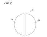
- FIG. 3 is a cross-sectional view of the electrostatic chuck according to the first embodiment of the present disclosure. It is a top view of the 1st electrode in a 1st embodiment of this indication.
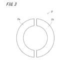
- FIG. 3 is a plan view of a second electrode according to the first embodiment of the present disclosure. It is a one part sectional view in other embodiments of this indication. It is a one part sectional view in other embodiments of this indication.
- An electrostatic chuck used for fixing and transporting a semiconductor wafer includes a mounting table on which an object to be processed is mounted, and a focus ring arranged on an outer peripheral portion of a mounting surface of the mounting table. And the focus ring are individually attracted by different first and second electrostatic attraction means.
- another electrostatic chuck is provided with an outer peripheral ring which is placed on the outer peripheral portion of a ceramic insulating plate having a main adsorption electrode directly or through an intermediate member, and the outer peripheral adsorption electrode provided on the outer peripheral portion is provided.
- the outer peripheral ring can be attracted and fixed to the outer peripheral portion.
- the focus ring or the outer peripheral ring which is an annular member arranged on the outer peripheral edge of the mounting surface or the outer peripheral portion of the insulating plate, is attracted.
- the width of the electrode of the electrostatic chuck is set to be narrow. Therefore, a sufficient suction force cannot be obtained, and the wafer and sample holder may be damaged due to movement of the focus ring or the outer peripheral ring during processing or transportation of the wafer.
- FIG. 1 is a vertical cross-sectional view of the electrostatic chuck 1.
- the electrostatic chuck 1 includes a support member 10, a sample holding member 20, and an annular body 30.
- the support member 10 is a member for supporting the sample holding member 20.
- the support member 10 has an upward support surface 11 that supports the sample holding member 20.
- the support member 10 is made of metal, and as the metal material, for example, aluminum can be used.
- the cross-sectional shape of the support member 10 in the horizontal direction is not particularly limited and may be circular or polygonal.
- the size of the support member 10 is not particularly limited, but when the horizontal cross-sectional shape is circular, for example, the diameter can be 200 to 500 mm and the thickness can be 10 to 100 mm.
- the sample holding member 20 includes a holding member main body 21 and an annular flange portion 22 that projects outward from an outer peripheral surface 25 of the holding member main body 21.
- the sample holding member 20 has a disc shape.
- the holding member main body 21 has a disc-like shape and has a circular upper surface on which a sample can be placed, that is, a placing surface 23, a circular supported surface 24 opposite to the placing surface 23, and an outer peripheral surface 25.
- a wafer which is a sample, is placed on the placing surface 23, and the wafer is fixed by electrostatic attraction.
- the supported surface 24 is joined to the supporting surface 11 of the supporting member 10 via the joining layer 40.
- the bonding layer 40 for example, an adhesive made of a resin material can be used. Silicon resin or the like can be used as the resin material.
- the holding member body 21 is made of, for example, a ceramic material.
- the ceramic material can be, but is not limited to, alumina, aluminum nitride, silicon nitride, yttria, and the like.
- the size of the holding member main body 21 is not particularly limited, but for example, the diameter can be 200 to 500 mm and the thickness can be 2 to 15 mm.
- the first electrode 26 for electrostatically attracting the sample is arranged inside the holding member main body 21, a first electrode 26 for electrostatically attracting the sample is arranged.
- the first electrode 26 includes two electrodes 26a and 26b.
- each of the two electrodes 26a and 26b has a substantially semicircular plate shape, and the semicircular chords are arranged so as to face each other.
- the entire first electrode 26 has a disk shape.
- the first electrode 26 is horizontally arranged in the holding member main body 21 such that the disk-shaped surface is parallel to the mounting surface 23 and the supported surface 24.
- the center of the first electrode 26 can be set such that the central axis is the same as the central axis of the holding member main body 21.
- a voltage is applied to the first electrode 26 from the outside.
- a positive voltage is applied to one of the two electrodes of the first electrode 26, and a negative voltage is applied to the other.
- the wafer mounted on the mounting surface 23 of the holding member main body 21 can be adsorbed and fixed.
- the first electrode 26 is formed of, for example, a metal material.
- the metal material can be, but is not limited to, platinum, tungsten, molybdenum, and the like.
- An outer peripheral surface 25 of the holding member main body 21 is provided with an annular flange portion 22 protruding outward.
- the collar portion 22 mounts the annular body 30 and mounts it on the opposite side of the mounting surface 28 on which the annular body 30 is fixed by electrostatic attraction, and the supported surface 29 bonded to the support member 10 via the bonding layer 40. have.
- the collar portion 22 is preferably integrated with the holding member body 21, but may be separable from the holding member body 21.
- the collar portion 22 is arranged below the outer peripheral surface 25, and the supported surface 29 of the collar portion 22 is arranged so as to be the same surface as the supported surface 24 of the holding member body 21. Has been done.
- the position of the collar portion 22 in the vertical direction with respect to the holding member main body 21 is not particularly limited, and may be located in the middle of the outer peripheral surface 25 of the holding member main body 21 in the vertical direction.
- the collar portion 22 is formed of, for example, a ceramic material.
- the ceramic material can be, but is not limited to, alumina, aluminum nitride, silicon nitride, yttria, and the like.
- the material forming the collar portion 22 may be the same as or different from that of the holding member main body 21.
- a second electrode 27 for electrostatic attraction of the annular body 30 is arranged inside the collar portion 22.
- the second electrode 27 is composed of two electrodes 27a and 27b, like the first electrode 26.
- Each of the electrodes 27a and 27b has a substantially semi-arcuate shape, and is arranged so that both ends of the arc are opposed to each other. By combining these two electrodes, the entire second electrode 27 has a ring shape.
- the second electrode 27 is horizontally arranged such that the ring surface is parallel to the mounting surface 28 and the supported surface 29 of the holding member body.
- Each of the second electrodes 27 extends from the collar portion 22 to the holding member main body 21, and the inner end is located inside the holding member main body 21.
- the inner end portion of the second electrode 27 means the inner peripheral portions of the electrodes 27a and 27b, and the same applies hereinafter.
- the inner end of the second electrode 27 is located below the first electrode 26 in the holding member body 21 in a side view.
- At least a part of the inner end of the second electrode 27 is located in a region overlapping the outer end of the first electrode 26 in plan view.
- the outer peripheral side end of the first electrode 26 means an outer peripheral part of the two electrodes 26a and 26b of the first electrode 26 in the circumferential direction.
- the second electrode 27 is preferably arranged at a position lower than the first electrode 26 in a side view, but may be arranged at a position higher than the first electrode 26 in a side view.
- the vertical distance between the upper surface of the second electrode 27 and the upper surface of the collar portion 22, that is, the mounting surface 28 is It is preferable that the distance between the upper surface of the one electrode 26 and the upper surface of the holding member main body 21, that is, the mounting surface 23 is larger than the vertical distance.
- a voltage is externally applied to the second electrode 27 as well as the first electrode 26.
- a positive voltage is applied to one of the two electrodes of the second electrode 27, and a negative voltage is applied to the other.
- the annular body 30 placed on the placing surface 28 of the collar portion 22 can be adsorbed and fixed.
- the annular body 30 is mounted on the mounting surface 28 of the collar portion 22, and covers the outer peripheral surface 25 of the holding member main body 21 and the upper surface of the collar portion 22, that is, the mounting surface 28.
- the annular body 30 has a mounting surface 31 and a suction surface 32.
- the mounting surface 31 is set to have the same height as the mounting surface 23 of the holding member main body 21 in a state where the annular body 30 is mounted on the flange portion 22. It is also possible to position the wafer mounted on the mounting surface 23 of the holding member main body 21 by projecting the outer peripheral edge of the mounting surface 31 of the annular body 30 upward.
- the cross section including the central axis of the annular body 30 is a quadrangle, but the cross section is not limited to a quadrangle and may be a polygon.
- the radius of the inner circumference of the annular body 30 is not particularly limited as long as it is larger than the radius of the outer circumference of the holding member main body 21.
- the annular body 30 is formed of, for example, a material capable of electrostatic adsorption such as silicon.
- the inner end of the second electrode 27 is located inside the holding member main body 21, not only the suction surface 32 of the annular body 30 but also the area facing the outer peripheral surface 25 of the holding member main body 21 is sucked. It is possible. Therefore, the ring-shaped body 30 is fixed with a strong suction force, and it is possible to prevent the wafer and the sample holding member 20 from being damaged when the ring-shaped body 30 moves during processing or transportation of the wafer.
- At least a part of the inner end portion of the second electrode 27 is located in a region overlapping with the outer end portion of the first electrode 26 in a plan view. It is possible to increase the suction force at the outer peripheral portion of the holding member main body 21 where there is no. Thereby, the wafer can be more strongly attracted.
- the second electrode 27 When the second electrode 27 is disposed at a position lower than the first electrode 26 in a side view, the vertical distance between the upper surface of the second electrode 27 and the upper surface of the collar portion 22, that is, the mounting surface 28, is reduced. , The upper surface of the first electrode 26 and the upper surface of the holding member main body 21, that is, the mounting surface 23 are made larger than the vertical distance, so that the flange portion 22 has a long distance from the second electrode 27. As a result, durability is improved and dielectric breakdown can be prevented. Further, in the holding member main body 21, since the distance between the first electrode 26 and the mounting surface 23 is short, the heat uniformity is improved.
- the electrostatic chuck 100 according to the second embodiment of the present disclosure will be described with reference to FIG.
- the same components as those in the first embodiment are designated by the same reference numerals and detailed description thereof will be omitted.
- the electrostatic chuck 100 of the present embodiment attracts a wafer placed on the placing surface 23 of the holding member main body 21 and the placing surface 31 of the annular body 30 of FIG. Fix it.
- the second electrode 102 has a substantially truncated cone shape, which is arranged inside the collar portion 22 in an upwardly inclined shape that is inclined upward toward the inner side in a side view.
- the second electrode 102 is composed of two electrodes as in the first embodiment, and the shapes of these electrodes when viewed from above in plan view are both substantially semi-circular. The two electrodes are arranged such that both ends of each arc are opposed to each other in a plan view from above. When these two electrodes are combined, the overall shape of the second electrode 102 as viewed from above is an annular shape.
- a voltage is externally applied to the second electrode 102.
- a positive voltage is applied to one of the two electrodes of the second electrode 102, and a negative voltage is applied to the other.
- the second electrode 102 has an upwardly inclined shape that inclines upward toward the inner side in a side view, the suction force at the outer peripheral portion of the holding member main body 21 where no electrode exists can be increased. Thereby, the wafer can be more strongly attracted.
- the electrostatic chuck 200 of the present embodiment attracts the wafers mounted on the mounting surface 23 of the holding member main body 21 and the mounting surface 31 of the annular body 30 of FIG. Fix it.
- the second electrode 202 has a substantially inverted truncated cone shape, which is arranged inside the collar portion 22 in a downwardly sloping shape that is inclined downward toward the inner side in a side view.
- the second electrode 202 is composed of two electrodes as in the other embodiments, and the shapes of these electrodes viewed in plan from above are substantially semi-circular. The two electrodes are arranged such that both ends of each arc are opposed to each other in a plan view from above. When these two electrodes are combined, the overall shape of the second electrode 202 when viewed from above is a ring shape.
- a voltage is externally applied to the second electrode 202.
- a positive voltage is applied to one of the two electrodes of the second electrode 202, and a negative voltage is applied to the other. Since the second electrode 202 has a downwardly inclined shape that inclines downward toward the inner side in a side view, the suction force in the vicinity of the outer periphery of the collar portion 22 where no electrode exists can be increased. Thereby, the annular body 30 can be more strongly adsorbed.
- the present disclosure can have the following embodiments.
- the electrostatic chuck of the present disclosure is a disc-shaped sample holding member, and has a disc-shaped holding member main body having a circular upper surface on which a sample can be placed, and an outer peripheral surface of the holding member main body.
- a sample holding member including a projecting annular collar portion, An annular body that is placed on the collar portion and covers the upper surface or the outer peripheral surface of the collar portion, A first electrode for electrostatically adsorbing a sample, which is arranged in the holding member body; A second electrode for electrostatic adsorption of the annular body, which is disposed in the collar portion, The inner end of the second electrode is located inside the holding member body.
- the second electrode for adsorbing the annular body that covers the outer peripheral surface of the holding member body extends to the holding member body and is located inside the holding member body.
- the wafer and the sample holding member can be prevented from being damaged due to movement of the annular body during processing or transportation of the wafer, because the wafer is fixed with a strong suction force.
- Electrostatic chuck 10
- Support member 11
- Support surface 20
- Sample holding member 21
- Holding member main body 22
- Collar portion 23 28, 31
- Mounting surface 24, 29
- Supported surface 25
- Outer peripheral surface 26
- Second electrodes 27a, 27b Electrode 30
- Annular body 32
Landscapes
- Container, Conveyance, Adherence, Positioning, Of Wafer (AREA)
- Drying Of Semiconductors (AREA)
Abstract
本開示の静電チャック(1)は、円板状の試料保持部材(20)であって、試料を載置可能な円形の上面を有する円板状の保持部材本体(21)と、保持部材本体(21)の外周面(25)から外方に突出する環状の鍔部(22)とを含む試料保持部材(20)と、鍔部(22)の上に載置される、鍔部(22)の上面または外周面を覆う環状体(30)と、保持部材本体(21)内に配設された、試料の静電吸着用の第1電極(26)と、鍔部(22)内に配設された、環状体(30)の吸着用の第2電極(27)と、を備えている。第2電極(27)の内方側端部は、保持部材本体(21)の内部に位置している。
Description
本開示は、半導体集積回路の製造工程または液晶表示装置の製造工程等において用いられる半導体ウエハ等の試料を保持するための試料保持具に配設される静電チャックに関するものである。
従来技術の一例は、特許文献1および特許文献2に記載されている。
本開示の静電チャックは、円板状の試料保持部材であって、試料を載置可能な円形の上面を有する円板状の保持部材本体と、該保持部材本体の外周面から外方に突出する環状の鍔部とを含む試料保持部材と、
前記鍔部の上に載置される、前記鍔部の上面または前記外周面を覆う環状体と、
前記保持部材本体内に配設された、試料の静電吸着用の第1電極と、
前記鍔部内に配設された、前記環状体の静電吸着用の第2電極と、を備え、
前記第2電極の内方側端部は、前記保持部材本体の内部に位置している構成である。
前記鍔部の上に載置される、前記鍔部の上面または前記外周面を覆う環状体と、
前記保持部材本体内に配設された、試料の静電吸着用の第1電極と、
前記鍔部内に配設された、前記環状体の静電吸着用の第2電極と、を備え、
前記第2電極の内方側端部は、前記保持部材本体の内部に位置している構成である。
本開示の目的、特色、および利点は、下記の詳細な説明と図面とからより明確になるであろう。
まず、本開示の静電チャックが基礎とする構成の静電チャックについて説明する。半導体ウエハの固定、搬送などに用いられる静電チャックは、被処理体を載置する載置台と、該載置台の載置面の外周縁部に配置されたフォーカスリングとを備え、被処理体とフォーカスリングとを、異なる第1、第2の静電吸着手段によって個別に吸着するようになっている。
また、他の静電チャックでは、主吸着用電極を有するセラミック絶縁板の外周部に直接または中間部材を介して載置される外周リングを備えており、外周部に設けられた外周吸着用電極によって、外周リングを外周部に吸着して固定することができる。
しかしながら、前記の本開示の静電チャックが基礎とする構成の静電チャックにおいては、載置面の外周縁部または絶縁板の外周部に配置された環状部材であるフォーカスリングまたは外周リングを吸着するための静電チャックの電極は、幅が狭く設定されている。そのため、十分な吸着力が得られず、ウエハの加工または搬送の際に、フォーカスリングまたは外周リングが動くことによって、ウエハおよび試料保持具が破損するおそれがある。
以下、本開示の第1実施形態に係る静電チャックについて、図面を参照して説明する。図1は、静電チャック1の垂直方向の断面図である。静電チャック1は、支持部材10、試料保持部材20および環状体30を備える。
<支持部材>
支持部材10は、試料保持部材20を支持するための部材である。支持部材10は、試料保持部材20を支持する上向きの支持面11を有する。支持部材10は、金属製であり、金属材料としては、例えば、アルミニウムを用いることができる。支持部材10の水平方向の断面形状は、特に限定されず、円形状または多角形状であってもよい。支持部材10の寸法は、特に限定されないが、前記水平方向の断面形状が円形の場合は、例えば、直径を200~500mmに、厚さを10~100mmとすることができる。
支持部材10は、試料保持部材20を支持するための部材である。支持部材10は、試料保持部材20を支持する上向きの支持面11を有する。支持部材10は、金属製であり、金属材料としては、例えば、アルミニウムを用いることができる。支持部材10の水平方向の断面形状は、特に限定されず、円形状または多角形状であってもよい。支持部材10の寸法は、特に限定されないが、前記水平方向の断面形状が円形の場合は、例えば、直径を200~500mmに、厚さを10~100mmとすることができる。
<試料保持部材>
試料保持部材20は、保持部材本体21および保持部材本体21の外周面25から外方に突出する環状の鍔部22を含む。試料保持部材20は円板状をなしている。
試料保持部材20は、保持部材本体21および保持部材本体21の外周面25から外方に突出する環状の鍔部22を含む。試料保持部材20は円板状をなしている。
<保持部材本体>
保持部材本体21は、円板状をなし、試料を載置可能な円形の上面、すなわち、載置面23と、載置面23の反対側に円形の被支持面24と、外周面25とを有する。載置面23には、試料であるウエハが載置され、ウエハは静電吸着により固定される。被支持面24は、支持部材10の支持面11と、接合層40を介して接合されている。接合層40としては、例えば、樹脂材料の接着剤を用いることができる。樹脂材料としては、シリコン樹脂などを用いることができる。
保持部材本体21は、円板状をなし、試料を載置可能な円形の上面、すなわち、載置面23と、載置面23の反対側に円形の被支持面24と、外周面25とを有する。載置面23には、試料であるウエハが載置され、ウエハは静電吸着により固定される。被支持面24は、支持部材10の支持面11と、接合層40を介して接合されている。接合層40としては、例えば、樹脂材料の接着剤を用いることができる。樹脂材料としては、シリコン樹脂などを用いることができる。
保持部材本体21は、例えば、セラミック材料で構成される。セラミック材料としては、アルミナ、窒化アルミニウム、窒化珪素、イットリア等とすることができるが、これらに限らない。保持部材本体21の寸法は、特に限定されないが、例えば、直径を200~500mmに、厚みを2~15mmにすることができる。
保持部材本体21の内部には、試料の静電吸着用の第1電極26が配設されている。図2に示すように、第1電極26は、2つの電極26aおよび電極26bからなる。本実施
形態においては、2つの電極26aおよび電極26bは、いずれも略半円板状であり、半
円の弦同士が対向するように配設されている。これら2つの電極が合わさって、第1電極26全体が円板状となっている。本実施形態においては、第1電極26は、保持部材本体21内に円板状の面が載置面23および被支持面24と平行になるように、水平に配設されている。第1電極26の中心は、該中心軸線が保持部材本体21の中心軸線と同一となるように設定することができる。
形態においては、2つの電極26aおよび電極26bは、いずれも略半円板状であり、半
円の弦同士が対向するように配設されている。これら2つの電極が合わさって、第1電極26全体が円板状となっている。本実施形態においては、第1電極26は、保持部材本体21内に円板状の面が載置面23および被支持面24と平行になるように、水平に配設されている。第1電極26の中心は、該中心軸線が保持部材本体21の中心軸線と同一となるように設定することができる。
第1電極26には外部から電圧が印加される。第1電極26の2つの電極の一方に正の電圧が印加され、他方に負の電圧が印加される。これにより、保持部材本体21の載置面23に載置されたウエハを吸着し、固定することができる。
第1電極26は、例えば、金属材料によって形成される。金属材料としては、白金、タングステン、モリブデン等とすることができるが、これらに限らない。
<鍔部>
保持部材本体21の外周面25には、外方に突出する環状の鍔部22が配設されている。鍔部22は、環状体30を載置し、静電吸着によって固定する載置面28および載置面28の反対側に、接合層40を介して支持部材10に接合される被支持面29を有している。鍔部22は、保持部材本体21と一体をなしていることが好ましいが、保持部材本体21から分離可能であってもよい。
保持部材本体21の外周面25には、外方に突出する環状の鍔部22が配設されている。鍔部22は、環状体30を載置し、静電吸着によって固定する載置面28および載置面28の反対側に、接合層40を介して支持部材10に接合される被支持面29を有している。鍔部22は、保持部材本体21と一体をなしていることが好ましいが、保持部材本体21から分離可能であってもよい。
本実施形態においては、鍔部22は、外周面25の下方に配設され、鍔部22の被支持面29は、保持部材本体21の被支持面24と同一の面をなすように配設されている。鍔部22の保持部材本体21に対する垂直方向の位置は特に限定されず、保持部材本体21の外周面25の垂直方向の中間に位置していてもよい。
鍔部22は、例えば、セラミック材料で形成される。セラミック材料としては、アルミナ、窒化アルミニウム、窒化珪素、イットリア等とすることができるが、これらに限らない。鍔部22を形成する材料は、保持部材本体21と同一の材料であっても、異なる材料であってもよい。
鍔部22内には、環状体30の静電吸着用の第2電極27が配設されている。第2電極27は、第1電極26と同様に2つの電極27aおよび電極27bからなる。電極27aおよび電極27bは、いずれも略半円弧状をなしており、円弧の両端が対向するように配設されている。これら2つの電極が合わさって、第2電極27全体が円環状となっている。本実施形態においては、第2電極27は、円環の面が保持部材本体の載置面28および被支持面29に平行になるように、水平に配設されている。
第2電極27は、いずれも鍔部22から保持部材本体21に延び、内方側端部は保持部材本体21の内部に位置している。ここで、第2電極27の内方側端部とは、電極27aおよび電極27bの内周部を意味し、以後も同様とする。本実施形態においては、第2電極27の内方側端部は、保持部材本体21内において、第1電極26より側面視下側に位置している。
本実施形態のように、保持部材本体21の内部において、第2電極27の内方側端部の少なくとも一部を、第1電極26の外周側端部と平面視において重なる領域に位置させることもできる。ここで、第1電極26の外周側端部とは、第1電極26の2つの電極26aおよび電極26bの周方向の外周部を意味する。
第2電極27は、第1電極26より側面視下側の位置に配設されることが好ましいが、第1電極26より側面視上側の位置に配設することもできる。第2電極27が第1電極26より側面視下側の位置に配設された場合、第2電極27の上面と鍔部22の上面、すなわち載置面28との上下方向の距離は、第1電極26の上面と保持部材本体21の上面、すなわち、載置面23との上下方向の距離よりも大きくすることが好ましい。
第2電極27にも、第1電極26と同様に、外部から電圧が印加される。第2電極27の2つの電極の一方に正の電圧が印加され、他方に負の電圧が印加される。これにより、鍔部22の載置面28に載置された環状体30を吸着し、固定することができる。
<環状体>
環状体30は、鍔部22の載置面28に載置され、保持部材本体21の外周面25および鍔部22の上面、すなわち、載置面28を覆っている。環状体30は、載置面31と吸着面32を有している。載置面31は、環状体30が鍔部22に載置された状態で、保持部材本体21の載置面23と同一の高さになるように設定されている。環状体30の載置面31の外周の周縁部を上方に突出させることによって、保持部材本体21の載置面23に載置されたウエハを位置決めすることもできる。
環状体30は、鍔部22の載置面28に載置され、保持部材本体21の外周面25および鍔部22の上面、すなわち、載置面28を覆っている。環状体30は、載置面31と吸着面32を有している。載置面31は、環状体30が鍔部22に載置された状態で、保持部材本体21の載置面23と同一の高さになるように設定されている。環状体30の載置面31の外周の周縁部を上方に突出させることによって、保持部材本体21の載置面23に載置されたウエハを位置決めすることもできる。
本実施形態において、環状体30の中心軸線を含む断面は四角形であるが、該断面は、四角形に限られず、多角形でもよい。環状体30の内周の半径は、保持部材本体21の外周の半径よりも大きければ、特に限定されない。環状体30は、例えば、シリコンなどの静電吸着が可能な材料によって形成されている。
第2電極27の内方側端部が保持部材本体21の内部に位置することによって、環状体30の吸着面32だけでなく、保持部材本体21の外周面25と対向する領域をも吸着することが可能である。そのため、環状体30が強い吸着力で固定され、ウエハの加工または搬送の際に、環状体30が動くことによって生じるウエハおよび試料保持部材20の破損を防止することができる。
また、保持部材本体21の内部において、第2電極27の内方側端部の少なくとも一部が、第1電極26の外周側端部と平面視において重なる領域に位置していることによって、電極が存在しない保持部材本体21の外周部での吸着力を増すことができる。これにより、ウエハをより強く吸着することができる。
第2電極27が第1電極26より側面視下側の位置に配設された場合、第2電極27の上面と鍔部22の上面、すなわち、載置面28、との上下方向の距離を、第1電極26の上面と保持部材本体21の上面、すなわち、載置面23、との上下方向の距離よりも大きくすることによって、鍔部22においては、第2電極27からの距離が長いために耐久性が向上し、絶縁破壊などが防止できる。また、保持部材本体21においては第1電極26と載置面23との距離が近いため、均熱性が向上する。
<第2実施形態>
次に、本開示の第2実施形態に係る静電チャック100について図4を参照して説明する。本実施形態では、第1実施形態と同様の構成要素には、第1実施形態と同一の符号を付して詳細な説明を省略する。
本実施形態の静電チャック100は、前記第1実施形態と同様に、図4の保持部材本体21の載置面23および環状体30の載置面31に載置されたウエハを吸着し、固定する。
次に、本開示の第2実施形態に係る静電チャック100について図4を参照して説明する。本実施形態では、第1実施形態と同様の構成要素には、第1実施形態と同一の符号を付して詳細な説明を省略する。
本実施形態の静電チャック100は、前記第1実施形態と同様に、図4の保持部材本体21の載置面23および環状体30の載置面31に載置されたウエハを吸着し、固定する。
本実施形態において、第2電極102は、鍔部22の内部で、側面視において内方側に向かって上に傾く上り傾斜状に配設された、略円錐台状をなしている。本実施形態においても、第2電極102は第1実施形態と同様に2つの電極からなり、これらを上方から平面視した形状は、いずれも略半円弧状をなしている。2つの電極は、上方からの平面視において、それぞれの円弧の両端が対向するように配設されている。これら2つの電極が合わさって、第2電極102全体を上方から平面視した形状は、円環状となっている。
第2電極102には、外部から電圧が印加される。第2電極102の2つの電極の一方に正の電圧が印加され、他方に負の電圧が印加される。第2電極102が側面視において内方側に向かって上に傾く上り傾斜状をなすことによって、電極が存在しない保持部材本体21の外周部での吸着力が増すことができる。これにより、ウエハをより強く吸着することができる。
<第3実施形態>
次に、本開示の第3実施形態に係る静電チャック200について図5を参照して説明する。本実施形態では、第1実施形態と同様の構成要素には、第1実施形態と同一の符号を付して詳細な説明を省略する。
次に、本開示の第3実施形態に係る静電チャック200について図5を参照して説明する。本実施形態では、第1実施形態と同様の構成要素には、第1実施形態と同一の符号を付して詳細な説明を省略する。
本実施形態の静電チャック200は、前記第1実施形態と同様に、図5の保持部材本体21の載置面23および環状体30の載置面31に載置されたウエハを吸着し、固定する。
第3実施形態において、第2電極202は、鍔部22の内部で、側面視において内方側に向かって下に傾く下り傾斜状に配設された、略逆円錐台状をなしている。本実施形態においても、第2電極202は他の実施形態と同様に2つの電極からなり、これらを上方から平面視した形状は、いずれも略半円弧状をなしている。2つの電極は、上方からの平面視において、それぞれの円弧の両端が対向するように配設されている。これら2つの電極が合わさって、第2電極202全体を上方から平面視した形状は、円環状となっている。
第2電極202には、外部から電圧が印加される。第2電極202の2つの電極の一方に正の電圧が印加され、他方に負の電圧が印加される。第2電極202が側面視において内方側に向かって下に傾く下り傾斜状をなすことによって、電極が存在しない鍔部22の外周近傍における吸着力を高めることができる。これにより、環状体30をより強く吸着することができる。
本開示は次の実施の形態が可能である。
本開示の静電チャックは、円板状の試料保持部材であって、試料を載置可能な円形の上面を有する円板状の保持部材本体と、該保持部材本体の外周面から外方に突出する環状の鍔部とを含む試料保持部材と、
前記鍔部の上に載置される、前記鍔部の上面または前記外周面を覆う環状体と、
前記保持部材本体内に配設された、試料の静電吸着用の第1電極と、
前記鍔部内に配設された、前記環状体の静電吸着用の第2電極と、を備え、
前記第2電極の内方側端部は、前記保持部材本体の内部に位置している構成である。
前記鍔部の上に載置される、前記鍔部の上面または前記外周面を覆う環状体と、
前記保持部材本体内に配設された、試料の静電吸着用の第1電極と、
前記鍔部内に配設された、前記環状体の静電吸着用の第2電極と、を備え、
前記第2電極の内方側端部は、前記保持部材本体の内部に位置している構成である。
本開示の静電チャックにおいては、保持部材本体の外周面を覆う環状体を吸着するための第2電極が、保持部材本体に延びて保持部材本体の内部に位置しているので、環状体が強い吸着力で固定され、ウエハの加工または搬送の際に、環状体が動くことによって生じるウエハおよび試料保持部材の破損を防止することができる。
本開示は、その精神または主要な特徴から逸脱することなく、他のいろいろな形態で実施できる。したがって、前述の実施形態はあらゆる点で単なる例示に過ぎず、本開示の範囲は特許請求の範囲に示すものであって、明細書本文には何ら拘束されない。さらに、特許請求の範囲に属する変形や変更は全て本開示の範囲内のものである。
1、100、200 静電チャック
10 支持部材
11 支持面
20 試料保持部材
21 保持部材本体
22 鍔部
23、28、31 載置面
24、29 被支持面
25 外周面
26、101、201 第1電極
26a、26b 電極
27、102、202 第2電極
27a、27b 電極
30 環状体
32 吸着面
40 接合層
10 支持部材
11 支持面
20 試料保持部材
21 保持部材本体
22 鍔部
23、28、31 載置面
24、29 被支持面
25 外周面
26、101、201 第1電極
26a、26b 電極
27、102、202 第2電極
27a、27b 電極
30 環状体
32 吸着面
40 接合層
Claims (5)
- 円板状の試料保持部材であって、試料を載置可能な円形の上面を有する円板状の保持部材本体と、該保持部材本体の外周面から外方に突出する環状の鍔部とを含む試料保持部材と、
前記鍔部の上に載置される、前記鍔部の上面または前記外周面を覆う環状体と、
前記保持部材本体内に配設された、試料の静電吸着用の第1電極と、
前記鍔部内に配設された、前記環状体の静電吸着用の第2電極と、を備え、
前記第2電極の内方側端部は、前記保持部材本体の内部に位置している、静電チャック。 - 前記第2電極の内方側端部は、前記保持部材本体内において、少なくともその一部が前記第1電極の外周側端部と平面視において重なる領域に位置している、請求項1に記載の静電チャック。
- 前記第2電極は、前記鍔部内で、側面視において内方側に向かって上に傾く上り傾斜状に配設されている、請求項1または2に記載の静電チャック。
- 前記第2電極は、前記鍔部内で、側面視において内方側に向かって下に傾く下り傾斜状に配設されている、請求項1または2に記載の静電チャック。
- 前記第2電極は、前記第1電極より側面視下側の位置に配設され、
前記第2電極の上面と前記鍔部の上面との上下方向の距離は、前記第1電極の上面と前記試料保持部材本体の上面との上下方向の距離よりも大きい、請求項1~4のいずれか1つに記載の静電チャック。
Priority Applications (1)
| Application Number | Priority Date | Filing Date | Title |
|---|---|---|---|
| JP2021502148A JP7174141B2 (ja) | 2019-02-22 | 2020-02-20 | 静電チャック |
Applications Claiming Priority (2)
| Application Number | Priority Date | Filing Date | Title |
|---|---|---|---|
| JP2019030278 | 2019-02-22 | ||
| JP2019-030278 | 2019-02-22 |
Publications (1)
| Publication Number | Publication Date |
|---|---|
| WO2020171180A1 true WO2020171180A1 (ja) | 2020-08-27 |
Family
ID=72143573
Family Applications (1)
| Application Number | Title | Priority Date | Filing Date |
|---|---|---|---|
| PCT/JP2020/006877 Ceased WO2020171180A1 (ja) | 2019-02-22 | 2020-02-20 | 静電チャック |
Country Status (2)
| Country | Link |
|---|---|
| JP (1) | JP7174141B2 (ja) |
| WO (1) | WO2020171180A1 (ja) |
Cited By (1)
| Publication number | Priority date | Publication date | Assignee | Title |
|---|---|---|---|---|
| JP2024512465A (ja) * | 2021-03-16 | 2024-03-19 | ラム リサーチ コーポレーション | 静電チャック用の三極電極配置 |
Citations (4)
| Publication number | Priority date | Publication date | Assignee | Title |
|---|---|---|---|---|
| JP2003163259A (ja) * | 2001-11-27 | 2003-06-06 | Taiheiyo Cement Corp | 内部電極を有するセラミック部品の製造方法および内部電極を有するセラミック部品 |
| JP3154930U (ja) * | 2009-08-19 | 2009-10-29 | 日本碍子株式会社 | 電極内蔵セラミックス部品 |
| JP2010183074A (ja) * | 2003-04-24 | 2010-08-19 | Tokyo Electron Ltd | プラズマ処理装置、フォーカスリング及び被処理体の載置装置 |
| JP2012204447A (ja) * | 2011-03-24 | 2012-10-22 | Covalent Materials Corp | 静電チャック |
-
2020
- 2020-02-20 WO PCT/JP2020/006877 patent/WO2020171180A1/ja not_active Ceased
- 2020-02-20 JP JP2021502148A patent/JP7174141B2/ja active Active
Patent Citations (4)
| Publication number | Priority date | Publication date | Assignee | Title |
|---|---|---|---|---|
| JP2003163259A (ja) * | 2001-11-27 | 2003-06-06 | Taiheiyo Cement Corp | 内部電極を有するセラミック部品の製造方法および内部電極を有するセラミック部品 |
| JP2010183074A (ja) * | 2003-04-24 | 2010-08-19 | Tokyo Electron Ltd | プラズマ処理装置、フォーカスリング及び被処理体の載置装置 |
| JP3154930U (ja) * | 2009-08-19 | 2009-10-29 | 日本碍子株式会社 | 電極内蔵セラミックス部品 |
| JP2012204447A (ja) * | 2011-03-24 | 2012-10-22 | Covalent Materials Corp | 静電チャック |
Cited By (1)
| Publication number | Priority date | Publication date | Assignee | Title |
|---|---|---|---|---|
| JP2024512465A (ja) * | 2021-03-16 | 2024-03-19 | ラム リサーチ コーポレーション | 静電チャック用の三極電極配置 |
Also Published As
| Publication number | Publication date |
|---|---|
| JP7174141B2 (ja) | 2022-11-17 |
| JPWO2020171180A1 (ja) | 2021-12-09 |
Similar Documents
| Publication | Publication Date | Title |
|---|---|---|
| US10410908B2 (en) | Substrate processing apparatus and substrate holding device | |
| US10964560B2 (en) | Substrate chuck and substrate bonding system including the same | |
| KR102474583B1 (ko) | 시료 유지구 | |
| JP7083923B2 (ja) | 静電チャック | |
| TWI762978B (zh) | 用於多層之靜電吸盤之接地機構及相關之方法 | |
| JP2020109806A (ja) | 試料保持具 | |
| CN114600230B (zh) | 基板吸引保持构造以及基板搬运机器人 | |
| JP7174141B2 (ja) | 静電チャック | |
| TW554465B (en) | Apparatus for supporting wafer in semiconductor process | |
| CN210575889U (zh) | 静电吸盘 | |
| JP2006253352A (ja) | 吸着装置 | |
| KR102611059B1 (ko) | 시료 유지구 | |
| JP7445386B2 (ja) | 基板保持部材および基板保持機構 | |
| JPS63226939A (ja) | ウエハ保持装置 | |
| JPH0823025A (ja) | ウェハチャック及びそのチャック部の製造方法 | |
| JP7697548B1 (ja) | 静電チャック | |
| JP2754420B2 (ja) | ウェーハ保持装置 | |
| JP2023146282A (ja) | 静電チャック装置 | |
| CN120376494A (zh) | 静电吸盘 | |
| CN121123097A (zh) | 静电吸盘 | |
| JP2023098194A (ja) | 基板保持部材 | |
| TWM517409U (zh) | 拋光設備 | |
| JP2020064951A (ja) | チャックテーブル | |
| JP2003007809A (ja) | ウエハ用衝撃吸収板およびウエハ用アクチュエータ | |
| TWM497849U (zh) | 晶圓承載盤 |
Legal Events
| Date | Code | Title | Description |
|---|---|---|---|
| 121 | Ep: the epo has been informed by wipo that ep was designated in this application |
Ref document number: 20758456 Country of ref document: EP Kind code of ref document: A1 |
|
| ENP | Entry into the national phase |
Ref document number: 2021502148 Country of ref document: JP Kind code of ref document: A |
|
| NENP | Non-entry into the national phase |
Ref country code: DE |
|
| 122 | Ep: pct application non-entry in european phase |
Ref document number: 20758456 Country of ref document: EP Kind code of ref document: A1 |