WO2020170082A1 - 半導体装置、および半導体装置の作製方法 - Google Patents
半導体装置、および半導体装置の作製方法 Download PDFInfo
- Publication number
- WO2020170082A1 WO2020170082A1 PCT/IB2020/051160 IB2020051160W WO2020170082A1 WO 2020170082 A1 WO2020170082 A1 WO 2020170082A1 IB 2020051160 W IB2020051160 W IB 2020051160W WO 2020170082 A1 WO2020170082 A1 WO 2020170082A1
- Authority
- WO
- WIPO (PCT)
- Prior art keywords
- oxide
- insulator
- conductor
- transistor
- film
- Prior art date
- Legal status (The legal status is an assumption and is not a legal conclusion. Google has not performed a legal analysis and makes no representation as to the accuracy of the status listed.)
- Ceased
Links
Images



























































Classifications
-
- H—ELECTRICITY
- H10—SEMICONDUCTOR DEVICES; ELECTRIC SOLID-STATE DEVICES NOT OTHERWISE PROVIDED FOR
- H10B—ELECTRONIC MEMORY DEVICES
- H10B12/00—Dynamic random access memory [DRAM] devices
-
- H—ELECTRICITY
- H10—SEMICONDUCTOR DEVICES; ELECTRIC SOLID-STATE DEVICES NOT OTHERWISE PROVIDED FOR
- H10B—ELECTRONIC MEMORY DEVICES
- H10B41/00—Electrically erasable-and-programmable ROM [EEPROM] devices comprising floating gates
- H10B41/70—Electrically erasable-and-programmable ROM [EEPROM] devices comprising floating gates the floating gate being an electrode shared by two or more components
-
- H—ELECTRICITY
- H10—SEMICONDUCTOR DEVICES; ELECTRIC SOLID-STATE DEVICES NOT OTHERWISE PROVIDED FOR
- H10D—INORGANIC ELECTRIC SEMICONDUCTOR DEVICES
- H10D30/00—Field-effect transistors [FET]
- H10D30/60—Insulated-gate field-effect transistors [IGFET]
- H10D30/67—Thin-film transistors [TFT]
- H10D30/6729—Thin-film transistors [TFT] characterised by the electrodes
- H10D30/673—Thin-film transistors [TFT] characterised by the electrodes characterised by the shapes, relative sizes or dispositions of the gate electrodes
- H10D30/6733—Multi-gate TFTs
- H10D30/6734—Multi-gate TFTs having gate electrodes arranged on both top and bottom sides of the channel, e.g. dual-gate TFTs
-
- H—ELECTRICITY
- H10—SEMICONDUCTOR DEVICES; ELECTRIC SOLID-STATE DEVICES NOT OTHERWISE PROVIDED FOR
- H10D—INORGANIC ELECTRIC SEMICONDUCTOR DEVICES
- H10D30/00—Field-effect transistors [FET]
- H10D30/60—Insulated-gate field-effect transistors [IGFET]
- H10D30/67—Thin-film transistors [TFT]
- H10D30/6729—Thin-film transistors [TFT] characterised by the electrodes
- H10D30/6737—Thin-film transistors [TFT] characterised by the electrodes characterised by the electrode materials
- H10D30/6739—Conductor-insulator-semiconductor electrodes
-
- H—ELECTRICITY
- H10—SEMICONDUCTOR DEVICES; ELECTRIC SOLID-STATE DEVICES NOT OTHERWISE PROVIDED FOR
- H10D—INORGANIC ELECTRIC SEMICONDUCTOR DEVICES
- H10D30/00—Field-effect transistors [FET]
- H10D30/60—Insulated-gate field-effect transistors [IGFET]
- H10D30/67—Thin-film transistors [TFT]
- H10D30/674—Thin-film transistors [TFT] characterised by the active materials
- H10D30/6755—Oxide semiconductors, e.g. zinc oxide, copper aluminium oxide or cadmium stannate
-
- H—ELECTRICITY
- H10—SEMICONDUCTOR DEVICES; ELECTRIC SOLID-STATE DEVICES NOT OTHERWISE PROVIDED FOR
- H10D—INORGANIC ELECTRIC SEMICONDUCTOR DEVICES
- H10D30/00—Field-effect transistors [FET]
- H10D30/60—Insulated-gate field-effect transistors [IGFET]
- H10D30/67—Thin-film transistors [TFT]
- H10D30/6757—Thin-film transistors [TFT] characterised by the structure of the channel, e.g. transverse or longitudinal shape or doping profile
-
- H—ELECTRICITY
- H10—SEMICONDUCTOR DEVICES; ELECTRIC SOLID-STATE DEVICES NOT OTHERWISE PROVIDED FOR
- H10D—INORGANIC ELECTRIC SEMICONDUCTOR DEVICES
- H10D30/00—Field-effect transistors [FET]
- H10D30/60—Insulated-gate field-effect transistors [IGFET]
- H10D30/68—Floating-gate IGFETs
-
- H—ELECTRICITY
- H10—SEMICONDUCTOR DEVICES; ELECTRIC SOLID-STATE DEVICES NOT OTHERWISE PROVIDED FOR
- H10D—INORGANIC ELECTRIC SEMICONDUCTOR DEVICES
- H10D30/00—Field-effect transistors [FET]
- H10D30/60—Insulated-gate field-effect transistors [IGFET]
- H10D30/69—IGFETs having charge trapping gate insulators, e.g. MNOS transistors
-
- H—ELECTRICITY
- H10—SEMICONDUCTOR DEVICES; ELECTRIC SOLID-STATE DEVICES NOT OTHERWISE PROVIDED FOR
- H10D—INORGANIC ELECTRIC SEMICONDUCTOR DEVICES
- H10D62/00—Semiconductor bodies, or regions thereof, of devices having potential barriers
- H10D62/40—Crystalline structures
- H10D62/405—Orientations of crystalline planes
-
- H—ELECTRICITY
- H10—SEMICONDUCTOR DEVICES; ELECTRIC SOLID-STATE DEVICES NOT OTHERWISE PROVIDED FOR
- H10D—INORGANIC ELECTRIC SEMICONDUCTOR DEVICES
- H10D84/00—Integrated devices formed in or on semiconductor substrates that comprise only semiconducting layers, e.g. on Si wafers or on GaAs-on-Si wafers
- H10D84/01—Manufacture or treatment
- H10D84/0123—Integrating together multiple components covered by H10D12/00 or H10D30/00, e.g. integrating multiple IGBTs
- H10D84/0126—Integrating together multiple components covered by H10D12/00 or H10D30/00, e.g. integrating multiple IGBTs the components including insulated gates, e.g. IGFETs
-
- H—ELECTRICITY
- H10—SEMICONDUCTOR DEVICES; ELECTRIC SOLID-STATE DEVICES NOT OTHERWISE PROVIDED FOR
- H10D—INORGANIC ELECTRIC SEMICONDUCTOR DEVICES
- H10D84/00—Integrated devices formed in or on semiconductor substrates that comprise only semiconducting layers, e.g. on Si wafers or on GaAs-on-Si wafers
- H10D84/01—Manufacture or treatment
- H10D84/02—Manufacture or treatment characterised by using material-based technologies
- H10D84/03—Manufacture or treatment characterised by using material-based technologies using Group IV technology, e.g. silicon technology or silicon-carbide [SiC] technology
- H10D84/038—Manufacture or treatment characterised by using material-based technologies using Group IV technology, e.g. silicon technology or silicon-carbide [SiC] technology using silicon technology, e.g. SiGe
-
- H—ELECTRICITY
- H10—SEMICONDUCTOR DEVICES; ELECTRIC SOLID-STATE DEVICES NOT OTHERWISE PROVIDED FOR
- H10D—INORGANIC ELECTRIC SEMICONDUCTOR DEVICES
- H10D99/00—Subject matter not provided for in other groups of this subclass
Definitions
- One embodiment of the present invention relates to a transistor, a semiconductor device, and an electronic device. Further, one embodiment of the present invention relates to a method for manufacturing a semiconductor device. Further, one embodiment of the present invention relates to a semiconductor wafer and a module.
- a semiconductor device refers to all devices that can function by utilizing semiconductor characteristics.
- a semiconductor circuit such as a transistor, a semiconductor circuit, an arithmetic unit, and a memory device are one mode of the semiconductor device.
- a display device (a liquid crystal display device, a light-emitting display device, or the like), a projection device, a lighting device, an electro-optical device, a power storage device, a storage device, a semiconductor circuit, an imaging device, an electronic device, or the like has a semiconductor device.
- one embodiment of the present invention is not limited to the above technical field.
- One embodiment of the invention disclosed in this specification and the like relates to an object, a method, or a manufacturing method. Further, one embodiment of the present invention relates to a process, a machine, a manufacture, or a composition (composition of matter).
- the transistor is widely applied to electronic devices such as an integrated circuit (IC) and an image display device (also simply referred to as a display device).
- IC integrated circuit
- image display device also simply referred to as a display device.
- Silicon-based semiconductor materials are widely known as semiconductor thin films applicable to transistors, but oxide semiconductors are drawing attention as other materials.
- Non-Patent Document 1 a CAAC (c-axis aligned crystalline) structure and an nc (nanocrystalline) structure, which are neither single crystal nor amorphous, have been found (see Non-Patent Document 1 and Non-Patent Document 2).
- Non-Patent Document 1 and Non-Patent Document 2 disclose a technique for manufacturing a transistor using an oxide semiconductor having a CAAC structure.
- One object of one embodiment of the present invention is to provide a semiconductor device in which variations in transistor characteristics are small. Another object of one embodiment of the present invention is to provide a highly reliable semiconductor device. Another object of one embodiment of the present invention is to provide a semiconductor device having favorable electric characteristics. Another object of one embodiment of the present invention is to provide a semiconductor device with high on-state current. Another object of one embodiment of the present invention is to provide a semiconductor device which can be miniaturized or highly integrated. Another object of one embodiment of the present invention is to provide a semiconductor device with low power consumption.
- One embodiment of the present invention includes a first oxide, a second oxide and a third oxide over the first oxide, and a first conductor over the second oxide.
- the region has a groove portion, the first oxide has a first layered crystal substantially parallel to the formation surface of the first oxide, and in the groove portion, the fourth oxide is the first layer. It has a second layered crystal substantially parallel to the oxide formation surface, and the concentration of aluminum atoms at the interface between the first oxide and the fourth oxide and in the vicinity thereof is 5.0 at% or less. Is a semiconductor device.
- Another embodiment of the present invention is the first oxide, the second oxide on the first oxide, and the third oxide, and the first oxide on the second oxide. And a second oxide on the third oxide, and a fourth oxide on the first oxide and between the second oxide and the third oxide.
- a fifth oxide on the fourth oxide, a first insulator on the fifth oxide, and a third conductor on the first insulator The oxide has a groove portion in a region which does not overlap with the second oxide and the third oxide, and the first oxide has a first layered shape which is substantially parallel to a formation surface of the first oxide.
- the fourth oxide has a second layered crystal that is substantially parallel to the surface where the first oxide is formed.
- the semiconductor device has a concentration of aluminum atoms of 2.0 atomic% or less at and near the interface.
- Another embodiment of the present invention is the first oxide, the second oxide on the first oxide, and the third oxide, and the first oxide on the second oxide. And a second oxide on the third oxide, and a fourth oxide on the first oxide and between the second oxide and the third oxide.
- a fifth oxide on the fourth oxide, a first insulator on the fifth oxide, and a third conductor on the first insulator The oxide has a groove portion in a region which does not overlap with the second oxide and the third oxide, and the first oxide has a first layered shape which is substantially parallel to a formation surface of the first oxide.
- the fourth oxide has a second layered crystal that is substantially parallel to the surface on which the first oxide is formed, and in the side wall of the groove, the fourth oxide has a crystal.
- the ab plane is continuously bonded, and the concentration of aluminum atoms at the interface between the first oxide and the fourth oxide and in the vicinity thereof is 2.0 at% or less.
- the difference between the height of the interface between the first oxide and the second oxide and the height of the interface between the fourth oxide and the fifth oxide is less than or equal to the thickness of the fourth oxide. Preferably.
- the first oxide, the fourth oxide, and the fifth oxide each have indium, the element M (M is gallium, aluminum, yttrium, or tin), and zinc,
- the atomic ratio of indium to the element M of the first oxide is larger than the atomic ratio of indium to the element M of the fifth oxide
- the atomic ratio of indium to the element M of the fourth oxide is 5 is preferably larger than the atomic ratio of indium to the element M of the oxide of No. 5.
- the first layered crystal and the second layered crystal have a c-axis substantially perpendicular to the surface on which the first oxide is formed.
- one or both of the first oxide and the fourth oxide have a CAAC structure in the vicinity of the lower end portion of the first conductor and in the vicinity of the lower end portion of the second conductor. Is preferred.
- a semiconductor device with less variation in transistor characteristics can be provided.
- a highly reliable semiconductor device can be provided.
- a semiconductor device having favorable electric characteristics can be provided.
- a semiconductor device with high on-state current can be provided.
- a semiconductor device which can be miniaturized or highly integrated can be provided.
- a semiconductor device with low power consumption can be provided.
- FIG. 1A and 1B are cross-sectional views of a semiconductor device which is one embodiment of the present invention.
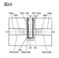
- FIG. 2A is a top view of a semiconductor device which is one embodiment of the present invention.
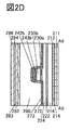
- 2B to 2D are cross-sectional views of a semiconductor device which is one embodiment of the present invention.
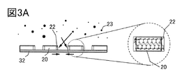
- 3A to 3D are diagrams illustrating a method for forming a CAAC-OS.
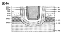
- 4A to 4C are cross-sectional views of a semiconductor device which is one embodiment of the present invention.
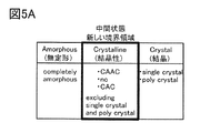
- FIG. 5A is a diagram for explaining the classification of the crystal structure of IGZO
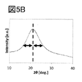
- FIG. 5B is a diagram for explaining the XRD spectrum of quartz glass.
- FIG. 5C is a diagram illustrating an XRD spectrum of crystalline IGZO.
- FIG. 5D is a diagram illustrating a microscopic electron beam diffraction pattern of crystalline IGZO.
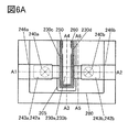
- FIG. 6A is a top view of a semiconductor device which is one embodiment of the present invention.
- 6B to 6D are cross-sectional views of the semiconductor device which is one embodiment of the present invention.
- FIG. 7A is a top view of a semiconductor device which is one embodiment of the present invention.
- 7B to 7D are cross-sectional views of a semiconductor device which is one embodiment of the present invention.
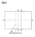
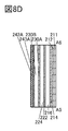
- FIG. 8A is a top view illustrating a method for manufacturing a semiconductor device which is one embodiment of the present invention.
- 8B to 8D are cross-sectional views illustrating a method for manufacturing a semiconductor device which is one embodiment of the present invention.
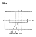
- 9A is a top view illustrating a method for manufacturing a semiconductor device which is one embodiment of the present invention.
- 9B to 9D are cross-sectional views illustrating a method for manufacturing a semiconductor device which is one embodiment of the present invention.
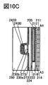
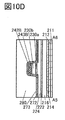
- 10A is a top view illustrating a method for manufacturing a semiconductor device which is one embodiment of the present invention.
- 10B to 10D are cross-sectional views illustrating a method for manufacturing a semiconductor device which is one embodiment of the present invention.
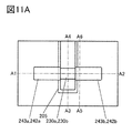
- 11A is a top view illustrating a method for manufacturing a semiconductor device which is one embodiment of the present invention.
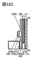
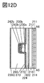
- 11B to 11D are cross-sectional views illustrating a method for manufacturing a semiconductor device which is one embodiment of the present invention.
- 12A is a top view illustrating a method for manufacturing a semiconductor device which is one embodiment of the present invention.
- 12B to 12D are cross-sectional views illustrating a method for manufacturing a semiconductor device which is one embodiment of the present invention.
- FIG. 13A is a top view illustrating a manufacturing method of a semiconductor device which is one embodiment of the present invention.
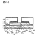
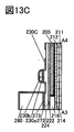
- 13B to 13D are cross-sectional views illustrating a method for manufacturing a semiconductor device which is one embodiment of the present invention.
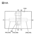
- 14A is a top view illustrating a method for manufacturing a semiconductor device which is one embodiment of the present invention.
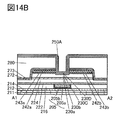
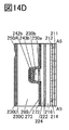
- 14B to 14D are cross-sectional views illustrating a method for manufacturing a semiconductor device which is one embodiment of the present invention.
- 15A is a top view illustrating a method for manufacturing a semiconductor device which is one embodiment of the present invention.
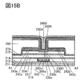
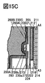
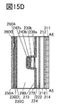
- 15B to 15D are cross-sectional views illustrating a method for manufacturing a semiconductor device which is one embodiment of the present invention.
- 16A is a top view illustrating a method for manufacturing a semiconductor device which is one embodiment of the present invention.
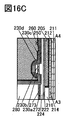
- 16B to 16D are cross-sectional views illustrating a method for manufacturing a semiconductor device which is one embodiment of the present invention.
- 17A is a top view illustrating a method for manufacturing a semiconductor device which is one embodiment of the present invention.
- 17B to 17D are cross-sectional views illustrating a method for manufacturing a semiconductor device which is one embodiment of the present invention.
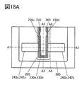
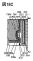
- 18A is a top view illustrating a method for manufacturing a semiconductor device which is one embodiment of the present invention.
- 18B to 18D are cross-sectional views illustrating a method for manufacturing a semiconductor device which is one embodiment of the present invention.
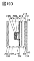
- FIG. 19A is a top view illustrating a method for manufacturing a semiconductor device which is one embodiment of the present invention.
- 19B to 19D are cross-sectional views illustrating a method for manufacturing a semiconductor device which is one embodiment of the present invention.
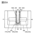
- 20A is a top view illustrating a method for manufacturing a semiconductor device which is one embodiment of the present invention.
- 20B to 20D are cross-sectional views illustrating a method for manufacturing a semiconductor device which is one embodiment of the present invention.
- 21A is a top view illustrating a method for manufacturing a semiconductor device which is one embodiment of the present invention.
- 21B to 21D are cross-sectional views illustrating a method for manufacturing a semiconductor device which is one embodiment of the present invention.
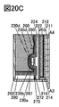
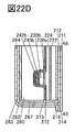
- 22A is a top view illustrating a method for manufacturing a semiconductor device which is one embodiment of the present invention.
- 22B to 22D are cross-sectional views illustrating a method for manufacturing a semiconductor device which is one embodiment of the present invention.
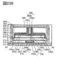
- FIG. 23A is a top view illustrating a method for manufacturing a semiconductor device which is one embodiment of the present invention.
- 23B to 23D are cross-sectional views illustrating a method for manufacturing a semiconductor device which is one embodiment of the present invention.
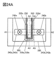
- 24A is a top view illustrating a method for manufacturing a semiconductor device which is one embodiment of the present invention.
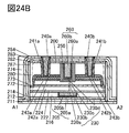
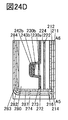
- 24B to 24D are cross-sectional views illustrating a method for manufacturing a semiconductor device which is one embodiment of the present invention.
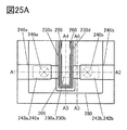
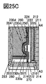
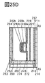
- 25A is a top view illustrating a method for manufacturing a semiconductor device which is one embodiment of the present invention.
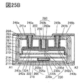
- 25B to 25D are cross-sectional views illustrating a method for manufacturing a semiconductor device which is one embodiment of the present invention.
- 26A and 26B are cross-sectional views of a semiconductor device according to one embodiment of the present invention.
- 27 is a cross-sectional view illustrating the structure of the memory device according to one embodiment of the present invention.
- FIG. 28 is a cross-sectional view illustrating the structure of the memory device according to one embodiment of the present invention.
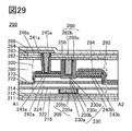
- FIG. 29 is a cross-sectional view of a semiconductor device according to one embodiment of the present invention.
- 30A and 30B are cross-sectional views of a semiconductor device according to one embodiment of the present invention.
- FIG. 31 is a cross-sectional view of a semiconductor device according to one embodiment of the present invention.
- 32 is a cross-sectional view of a semiconductor device according to one embodiment of the present invention.
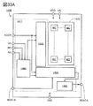
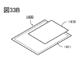
- 33A and 33B are block diagrams illustrating a structural example of a memory device according to one embodiment of the present invention.
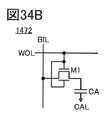
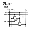
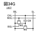
- 34A to 34H are circuit diagrams each illustrating a structural example of a memory device according to one embodiment of the present invention.
- FIG. 29 is a cross-sectional view of a semiconductor device according to one embodiment of the present invention.
- 30A and 30B are cross-sectional views of a semiconductor device according to one embodiment of the present invention.
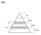
- 35 is a diagram showing various storage devices layer by layer.
- 36A and 36B are schematic views of a semiconductor device according to one embodiment of the present invention.
- 37A and 37B are diagrams illustrating an example of an electronic component.
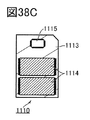
- 38A to 38E are schematic views of a memory device according to one embodiment of the present invention.
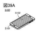
- 39A to 39H are diagrams illustrating electronic devices according to one embodiment of the present invention.
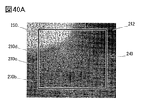
- 40A and 40B are TEM images according to this example.
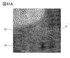
- FIG. 41A is a TEM image according to this example.
- 41B to 41D are FFT images according to this example.
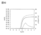
- FIG. 42 is a graph showing the measurement results of Id-Vg characteristics according to this example.
- FIG. 43A is a graph showing variations in Vsh according to this example.
- FIG. 43B is a graph showing variations in S value according to the present embodiment.
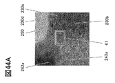
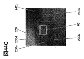
- 44A to 44C are TEM images according to this example.
- FIG. 45 is a graph showing the measurement results of the aluminum concentration according to
- the size, the layer thickness, or the region may be exaggerated for clarity. Therefore, it is not necessarily limited to that scale.
- the drawings schematically show ideal examples, and are not limited to the shapes or values shown in the drawings.
- a layer, a resist mask, or the like may be unintentionally reduced due to a process such as etching, but this may not be reflected in the drawing for easy understanding.
- the same reference numerals are commonly used in different drawings for the same portions or portions having similar functions, and repeated description thereof may be omitted.
- the hatch pattern may be the same and may not be given a reference numeral in particular.
- top view also referred to as “plan view”
- perspective view some of the constituent elements may be omitted for easy understanding of the invention.
- description of some hidden lines may be omitted.
- the ordinal numbers given as the first, second, etc. are used for convenience, and do not indicate the process order or the stacking order. Therefore, for example, “first” can be replaced with “second” or “third” as appropriate.
- the ordinal numbers described in this specification and the like may be different from the ordinal numbers used to specify one embodiment of the present invention.
- connection relations are not limited to the predetermined connection relations, for example, the connection relations shown in the drawings or the texts, and other connection relations than the connection relations shown in the drawings or the texts are also disclosed in the drawings or the texts.
- X and Y are objects (for example, devices, elements, circuits, wirings, electrodes, terminals, conductive films, layers, etc.).
- a transistor is an element having at least three terminals including a gate, a drain, and a source. And a region (hereinafter, also referred to as a channel formation region) in which a channel is formed between the drain (drain terminal, drain region or drain electrode) and the source (source terminal, source region or source electrode), A current can be made to flow between the source and the drain via the channel formation region.
- a channel formation region refers to a region in which a current mainly flows.
- the functions of the source and drain may be switched when adopting transistors of different polarities or when the direction of current changes during circuit operation. Therefore, in this specification and the like, the terms source and drain can be interchanged in some cases.
- the channel length means, for example, in a top view of a transistor, a region where a semiconductor (or a portion where current flows in the semiconductor when the transistor is on) and a gate electrode overlap with each other, or a source in a channel formation region.
- the channel length does not necessarily have the same value in all regions. That is, the channel length of one transistor may not be set to one value. Therefore, in this specification, the channel length is any one value, the maximum value, the minimum value, or the average value in the channel formation region.
- the channel width is, for example, in a top view of a transistor, a region in which a semiconductor (or a portion of a semiconductor in which a current flows) and a gate electrode overlap with each other in a top view of the transistor, or a channel formation direction in a channel formation region. Refers to the length of the channel formation region in the vertical direction. Note that in one transistor, the channel width does not necessarily have the same value in all regions. That is, the channel width of one transistor may not be set to one value. Therefore, in this specification, the channel width is any one value, the maximum value, the minimum value, or the average value in the channel formation region.
- a channel width in a region where a channel is actually formed (hereinafter also referred to as an “effective channel width”) and a channel width shown in a top view of the transistor depending on the structure of the transistor. (Hereinafter, also referred to as “apparent channel width”).
- the effective channel width becomes larger than the apparent channel width, and the effect thereof may not be negligible.
- the proportion of the channel formation region formed in the side surface of the semiconductor may be large. In that case, the effective channel width is larger than the apparent channel width.
- channel width when simply described as channel width, it may indicate an apparent channel width.
- channel width when simply described as a channel width, it may refer to an effective channel width. Note that the channel length, channel width, effective channel width, apparent channel width, and the like can be determined by analyzing a cross-sectional TEM image or the like.
- the impurities of the semiconductor refer to, for example, components other than the main components that constitute the semiconductor.
- an element having a concentration of less than 0.1 atomic% can be said to be an impurity. Due to the inclusion of impurities, for example, the defect level density of the semiconductor may increase and the crystallinity may decrease.
- examples of impurities that change the characteristics of the semiconductor include a Group 1 element, a Group 2 element, a Group 13 element, a Group 14 element, a Group 15 element, and an oxide semiconductor.
- transition metals other than the main component such as hydrogen, lithium, sodium, silicon, boron, phosphorus, carbon, and nitrogen. Water may also function as an impurity.
- the oxide semiconductor to an oxygen vacancy V O: also referred to as oxygen vacancy
- silicon oxynitride has a higher oxygen content than nitrogen as its composition. Further, silicon oxynitride has a composition that contains more nitrogen than oxygen.
- the term “insulator” can be restated as an insulating film or an insulating layer.
- the term “conductor” can be referred to as a conductive film or a conductive layer.
- the term “semiconductor” can be restated as a semiconductor film or a semiconductor layer.
- parallel means a state in which two straight lines are arranged at an angle of ⁇ 10 degrees or more and 10 degrees or less. Therefore, a case of -5 degrees or more and 5 degrees or less is also included.
- substantially parallel means a state in which two straight lines are arranged at an angle of ⁇ 30 degrees or more and 30 degrees or less.
- vertical means a state in which two straight lines are arranged at an angle of 80 degrees or more and 100 degrees or less. Therefore, a case of 85 degrees or more and 95 degrees or less is also included.
- generally vertical means a state in which two straight lines are arranged at an angle of 60 degrees or more and 120 degrees or less.
- a metal oxide is a metal oxide in a broad sense. Metal oxides are classified into oxide insulators, oxide conductors (including transparent oxide conductors), oxide semiconductors (Oxide Semiconductor or simply OS), and the like. For example, when a metal oxide is used for a semiconductor layer of a transistor, the metal oxide may be referred to as an oxide semiconductor. That is, when the term “OS transistor” is used, it can be referred to as a transistor including a metal oxide or an oxide semiconductor.
- normally-off means that when a potential is not applied to the gate or a ground potential is applied to the gate, the drain current per channel width of 1 ⁇ m flowing in the transistor is 1 ⁇ 10 ⁇ at room temperature. It means 20 A or less, 1 ⁇ 10 ⁇ 18 A or less at 85° C., or 1 ⁇ 10 ⁇ 16 A or less at 125° C.
- FIGS. 1A and 1B are partial enlarged views of the transistor 200
- FIGS. 2A to 2D are a top view and a cross-sectional view of a semiconductor device including the transistor 200
- FIG. 2A is a top view of the semiconductor device.
- 2B to 2D are cross-sectional views of the semiconductor device.
- FIG. 2B is a cross-sectional view of a portion indicated by dashed-dotted line A1-A2 in FIG. 2A and also a cross-sectional view of the transistor 200 in the channel length direction.
- FIG. 1A is an enlarged view of the vicinity of the channel formation region in FIG. 2B
- FIG. 1A is an enlarged view of the vicinity of the channel formation region in FIG. 2B
- FIG. 1B is an enlarged view of the vicinity of the interface between the oxide 243a and the oxide 230c in FIG. 1A.
- 2C is a cross-sectional view of a portion indicated by dashed-dotted line A3-A4 in FIG. 2A and is also a cross-sectional view of the transistor 200 in the channel width direction.
- FIG. 2D is a cross-sectional view of a portion indicated by alternate long and short dash line A5-A6 in FIG. 2A. In the top view of FIG. 2A, some elements are omitted for clarity of the drawing.
- a semiconductor device of one embodiment of the present invention includes an insulator 211 over a substrate (not shown), an insulator 212 over the insulator 211, an insulator 214 over the insulator 212, and a transistor 200 over the insulator 214. And an insulator 280 over the transistor 200, an insulator 282 over the insulator 280, an insulator 283 over the insulator 282, and an insulator 284 over the insulator 283.
- the insulator 211, the insulator 212, the insulator 214, the insulator 280, the insulator 282, the insulator 283, and the insulator 284 function as an interlayer film.
- a conductor 240 (a conductor 240a and a conductor 240b) which is electrically connected to the transistor 200 and serves as a plug is included.
- the insulator 241 (the insulator 241a and the insulator 241b) is provided in contact with the side surface of the conductor 240 which functions as a plug.
- a conductor 246 (a conductor 246a and a conductor 246b) which is electrically connected to the conductor 240 and serves as a wiring is provided over the insulator 284 and the conductor 240.
- An insulator 286 is provided over the conductor 246 and the insulator 284.
- the insulator 241a is provided in contact with the inner walls of the openings of the insulator 272, the insulator 273, the insulator 280, the insulator 282, the insulator 283, and the insulator 284, and the conductor 240a is provided in contact with the side surface of the insulator 241a.
- the first conductor is provided, and the second conductor of the conductor 240a is further provided inside.
- the insulator 241b is provided in contact with the inner walls of the openings of the insulator 272, the insulator 273, the insulator 280, the insulator 282, the insulator 283, and the insulator 284, and the conductor is provided in contact with the side surface of the insulator 241b.
- the first conductor of 240b is provided, and the second conductor of the conductor 240b is further provided inside.
- the height of the upper surface of the conductor 240 and the height of the upper surface of the insulator 284 in a region overlapping with the conductor 246 can be approximately the same.
- the transistor 200 has a structure in which the first conductor of the conductor 240 and the second conductor of the conductor 240 are stacked, the present invention is not limited to this.
- the conductor 240 may have a single-layer structure or a stacked structure including three or more layers. When the structure has a laminated structure, an ordinal number may be given in order of formation to distinguish them.
- the transistor 200 includes an insulator 216 over an insulator 214, an insulator 214, and an electric conductor 205 (an electric conductor 205a and an electric conductor 205) arranged so as to be embedded in the insulator 216. 205b), the insulator 222 on the insulator 216 and the conductor 205, the insulator 224 on the insulator 222, the oxide 230a on the insulator 224, and the oxide 230b on the oxide 230a.
- the oxide 243 (the oxide 243a and the oxide 243b) and the oxide 230c over the oxide 230b, the conductor 242a over the oxide 243a, the conductor 242b over the oxide 243b, and the oxide 230c.
- the upper surface of the conductor 260 is arranged so as to substantially match the upper surfaces of the insulator 250, the oxide 230d, and the oxide 230c.
- the insulator 282 is in contact with the top surfaces of the conductor 260, the insulator 250, the oxide 230d, the oxide 230c, and the insulator 280.
- An opening reaching the oxide 230b is provided in the insulator 280, the insulator 273, and the insulator 272.
- the oxide 230d, the oxide 230c, the insulator 250, and the conductor 260 are arranged in the opening.
- the conductor 260, the insulator 250, the oxide 230d, and the oxide 230c are provided between the conductor 242a and the oxide 243a and the conductor 242b and the oxide 243b.
- the insulator 250 has a region in contact with the side surface of the conductor 260 and a region in contact with the bottom surface of the conductor 260.
- the oxide 230c includes a region in contact with the oxide 230b, a region overlapping with a side surface of the conductor 260 with the insulator 250 interposed therebetween, and a bottom surface of the conductor 260 with the insulator 250 interposed therebetween. And a region overlapping with.
- the oxide 230 is disposed over the insulator 224, the oxide 230b, the oxide 230b, the oxide 230b, the oxide 230b, and the oxide 230b. It is preferable to have the oxide 230c which is in contact with the oxide 230c and the oxide 230d which is provided over the oxide 230c. With the oxide 230a below the oxide 230b, diffusion of impurities into the oxide 230b from a structure formed below the oxide 230a can be suppressed. Further, by including the oxide 230d over the oxide 230c, diffusion of impurities from the structure formed above the oxide 230d into the oxide 230c can be suppressed.
- the oxide 230 has a structure in which four layers of the oxide 230a, the oxide 230b, the oxide 230c, and the oxide 230d are stacked; however, the present invention is not limited to this. ..
- a single layer of oxide 230b, a two-layer structure of oxide 230a and oxide 230b, a two-layer structure of oxide 230b and oxide 230c, a three-layer structure of oxide 230a, oxide 230b, and oxide 230c Alternatively, a stacked-layer structure having five or more layers may be provided, or each of the oxide 230a, the oxide 230b, the oxide 230c, and the oxide 230d may have a stacked structure.
- the conductor 260 functions as a first gate (also referred to as a top gate) electrode, and the conductor 205 functions as a second gate (also referred to as a back gate) electrode.
- the insulator 250 functions as a first gate insulator and the insulator 224 functions as a second gate insulator.
- the conductor 242a functions as one of the source and the drain, and the conductor 242b functions as the other of the source and the drain.
- the oxide 230 functions as a channel formation region.
- the oxide 230 including the channel formation region (the oxide 230a, the oxide 230b, the oxide 230c, and the oxide 230d) is provided with a metal oxide functioning as a semiconductor (hereinafter also referred to as an oxide semiconductor). It is preferable to use.
- the metal oxide that functions as a semiconductor preferably has a bandgap of 2 eV or more, more preferably 2.5 eV or more.
- the off-state current of the transistor can be reduced by using the metal oxide having a wide band gap.
- an In-M-Zn oxide containing indium, element M, and zinc (the element M is aluminum, gallium, yttrium, tin, copper, vanadium, beryllium, boron, titanium, iron, nickel, germanium).
- the oxide 230 an In—Ga oxide, an In—Zn oxide, or an indium oxide may be used.
- the atomic ratio of In to the element M in the metal oxide used for the oxide 230b or the oxide 230c is larger than the atomic ratio of In to the element M in the metal oxide used for the oxide 230a or the oxide 230d. It is preferably large. In this manner, by disposing the oxide 230d on the oxide 230b or the oxide 230c, diffusion of impurities into the oxide 230b or the oxide 230c from the structure formed above the oxide 230d is prevented. Can be suppressed. In addition, since the oxides 230a to 230d have a common element (main component) other than oxygen, defects at interfaces of the oxide 230a, the oxide 230b, the oxide 230c, and the oxide 230d can be obtained.
- main component main component
- the level density can be lowered.
- the main path of carriers is the oxide 230b, the oxide 230c, or the vicinity thereof, for example, the interface between the oxide 230b and the oxide 230c. Since the density of defect states at the interface between the oxide 230b and the oxide 230c can be lowered, the influence of interface scattering on carrier conduction is small and a high on-state current can be obtained.
- the oxide 230b and the oxide 230c preferably have crystallinity.
- the oxide 230d may have crystallinity.
- CAAC-OS has c-axis orientation, and has a crystal structure in which a plurality of nanocrystals are connected in the ab plane direction and have strain.
- the strain refers to a portion where the orientation of the lattice arrangement is changed between a region where the lattice arrangement is uniform and another region where the lattice arrangement is uniform in the region where a plurality of nanocrystals are connected.
- ⁇ Nanocrystals are basically hexagonal, but they are not limited to regular hexagons and may be non-regular hexagons.
- the strain may have a lattice arrangement such as a pentagon and a heptagon.
- a lattice arrangement such as a pentagon and a heptagon.
- the crystal structure in which a clear grain boundary is confirmed is called a so-called polycrystal.
- the crystal grain boundaries serve as recombination centers and carriers are captured, which is likely to cause a decrease in on-state current of the transistor or a decrease in field-effect mobility. Therefore, the CAAC-OS in which clear crystal grain boundaries are not confirmed is one of crystalline oxides having a crystal structure suitable for a semiconductor layer of a transistor.
- a structure containing Zn is preferable for forming the CAAC-OS.
- In—Zn oxide and In—Ga—Zn oxide are preferable because they can suppress generation of crystal grain boundaries more than In oxide.
- the CAAC-OS is a layered crystal in which a layer containing indium and oxygen (hereinafter, an In layer) and a layer containing elements M, zinc, and oxygen (hereinafter, a (M,Zn) layer) are stacked. It tends to have a structure (also called a layered structure).
- indium and the element M can be replaced with each other, and when the element M of the (M,Zn) layer is replaced with indium, it can be expressed as an (In,M,Zn) layer. Further, when the indium in the In layer is replaced with the element M, it can be expressed as an (In,M) layer.
- the nanocluster 20 has a flat plate-like structure in which a (M,Zn) layer is located on the surface, and is composed of two (M,Zn) layers and an In layer located between them.
- the particles 23 reach the surface of the substrate 32.
- the particles 23 are more likely to be bonded to the side surface than the upper surface of the nanocluster 20. Therefore, the particles 23 preferentially adhere to the side surface of the nanocluster 20 so as to fill the region where the nanocluster 20 is not formed.
- the particles 23 are chemically connected to the nanoclusters 20 to form lateral growth portions 22 when the bonds are activated (see FIG. 3A). It can be said that the particles 23 enter the region between the nanoclusters 20.
- FIG. 3A an enlarged view of the nanocluster 20 is also shown, and a schematic view of the crystal structure is also shown in the nanocluster 20.
- the lateral growth portion 22 grows laterally (also referred to as lateral growth) so as to fill a region 26 between the nanoclusters 20 and 20 (the region 26 can also be referred to as Lateral Growth Buffer Region (LGBR)).
- the lateral direction refers to, for example, a direction perpendicular to the c-axis in the nanocluster 20.
- the oxygen diffused via LGBR adheres to the particles 23, and the particles 23 again. Is also likely to attach, which is likely to occur. It is estimated that the solid phase growth in the lateral direction occurs due to this repetition.
- lateral growth of the lateral growth portions 22 causes the lateral growth portions 22 to collide with each other.
- the nanoclusters 20 adjacent to each other are connected to each other by using the portion where the lateral growth portion 22 collides as the connecting portion 27 (see FIG. 3B). That is, the connecting portion 27 is formed in the region 26. It can be said that the particles 23 fill the regions 26 between the nanoclusters 20 by forming the lateral growth portion 22 on the side surface of the nanocluster 20 and growing laterally. In this way, the lateral growth portion 22 is formed until the region where the nano clusters 20 are not formed is filled.
- the layered crystal structure stably exists in a wide composition range, and the strength of the bond between the metal atom and the oxygen atom and the equilibrium distance are different for each metal atom. Therefore, it is presumed that the crystal structure of InMZnO 4 is tolerant to strain. Therefore, since the particles 23 smoothly connect (anchor) between the nanoclusters 20, a crystal structure different from that of a single crystal or a polycrystal is formed in the connecting portion 27. In other words, a strained crystal structure is formed in the connection part 27 between the nanoclusters 20.
- the crystal structure whose upper surface is a hexagon may be deformed to become a pentagon or a heptagon.
- the region filling the space between the nanoclusters 20 is a distorted crystal region, it is considered inappropriate to refer to the region as an amorphous structure.
- new nanoclusters 20 are formed with the plane side facing the surface of the substrate 32.
- the particles 23 are deposited so as to fill the region where the nanoclusters 20 are not formed, thereby forming the lateral growth portion 22 (see FIG. 3C).
- the particles 23 adhere to the side surfaces of the nanoclusters 20 and the laterally grown portions 22 laterally grow to connect the nanoclusters 20 in the second layer (see FIG. 3D).
- nano-clusters will be deposited on the surface (formation surface) of the substrate by the film formation model as described above. Since the CAAC-OS can be deposited even when the surface to be formed does not have a crystal structure, it is found that the above-described deposition model, which is a growth mechanism different from epitaxial growth, has high validity.
- the CAAC-OS is a metal oxide that has a dense structure with high crystallinity and has few impurities and defects (such as oxygen deficiency Vo).
- the metal oxide having CAAC-OS has stable physical properties. Therefore, the metal oxide containing CAAC-OS is highly heat resistant and highly reliable.
- a transistor including an oxide semiconductor when impurities and oxygen vacancies are present in a region where a channel is formed in the oxide semiconductor, electric characteristics are likely to vary and reliability may be deteriorated.
- the hydrogen of oxygen vacancies near defects containing the hydrogen to the oxygen deficiency (hereinafter, may be referred to as V O H.) To form, which may produce electrons as carriers. Therefore, when an oxygen deficiency is included in a region where a channel is formed in the oxide semiconductor, the transistor has a normally-on characteristic (the channel exists even when voltage is not applied to the gate electrode and current flows in the transistor). Flow characteristics). Therefore, it is preferable that impurities and oxygen vacancies be reduced as much as possible in a region where a channel is formed in the oxide semiconductor. In other words, it is preferable that the region where a channel is formed in the oxide semiconductor have a reduced carrier concentration and be i-type (intrinsic) or substantially i-type.
- the CAAC-OS as described above for the oxide 230b and the oxide 230c, impurities and oxygen vacancies can be reduced in the region where a channel is formed in the oxide semiconductor. it can. Accordingly, it is possible to provide a transistor in which fluctuations in electrical characteristics are suppressed, stable electrical characteristics are obtained, and reliability is improved.
- the surface of the oxide 230b which is the bottom of the opening, may be damaged.
- crystal defects such as oxygen vacancies are formed, and impurities (metal elements such as hydrogen, nitrogen, silicon, or aluminum) may exist.
- impurities metal elements such as hydrogen, nitrogen, silicon, or aluminum
- oxygen deficiency and impurities such as hydrogen are likely to exist, so that the reaction V O +H ⁇ V OH is likely to occur.
- the damaged region so that V O H is heavily formed. Therefore, even if the oxide 230c is formed over the damaged region of the oxide 230b, the transistor is likely to have normally-on characteristics.
- the state of the damaged region varies in the plane of the substrate, which causes variations in the characteristics of the semiconductor device having the transistor.
- the above damaged region can be removed by providing a groove above the oxide 230b.
- the oxide 230c including the CAAC-OS can be formed in the groove portion of the oxide 230b from which the damaged region is removed.
- a groove portion be provided in the oxide 230b and the oxide 230c having a CAAC-OS be embedded in the groove portion in a cross-sectional view of the transistor in the channel length direction.
- the oxide 230c is arranged so as to cover the inner wall (side wall and bottom surface) of the groove. Further, the film thickness of the oxide 230c is preferably about the same as the depth of the groove.
- the transistor by reducing the influence of impurities such as V O H, it is possible to form a channel in the oxide 230c. Thereby, good electrical characteristics can be given to the transistor. Furthermore, a semiconductor device with less variation in transistor characteristics and favorable reliability can be provided.
- FIGS. 1A and 1B are enlarged cross-sectional views of the transistor 200 and its vicinity. Note that the dashed lines shown in FIGS. 1A and 1B indicate crystal layers in the oxide 230b and the oxide 230c.
- the oxide 230b includes a layered crystal having a crystal layer extending in the ab plane direction and a c-axis perpendicular to the ab plane direction.
- the arrow shown in FIG. 1B indicates the c-axis of the crystal.
- the c-axis preferably faces a direction substantially perpendicular to the formation surface or the top surface of the oxide 230b. Therefore, as shown in FIG. 1, the oxide 230b has a region in which a crystal layer is extended so as to be substantially parallel to the upper surface of the oxide 230b.
- a groove is formed above the oxide 230b.
- the groove portion corresponds to the bottom portion of the opening formed in the insulator 280 or the like for embedding the conductor 260 or the like. That is, the groove portion overlaps with the conductor 260, the insulator 250, the oxide 230d, and the oxide 230c.
- the sidewall of the groove is substantially perpendicular to the surface on which the oxide 230b is formed.
- the side wall of the opening is substantially perpendicular to the surface on which the oxide 230b is formed.
- the depth of the groove portion of the oxide 230b substantially coincides with the film thickness of the oxide 230c.
- the height of the interface between the oxide 230b and the oxide 243 substantially matches the height of the interface between the oxide 230c and the oxide 230d.
- the difference between the height of the interface between the oxide 230b and the oxide 243 and the height of the interface between the oxide 230c and the oxide 230d is preferably less than or equal to the thickness of the oxide 230c. Is more preferably half or less.
- the oxide 230c includes a layered crystal having a crystal layer extending in the ab plane direction and a c-axis perpendicular to the ab plane direction. ..
- the c-axis preferably points in a direction substantially perpendicular to the formation surface or the top surface of the oxide 230c. Therefore, as illustrated in FIG. 1, the oxide 230c includes a region in which a crystal layer extends so as to be substantially parallel to the top surface of the oxide 230b, an oxide 243, a conductor 242, an insulator 272, and an insulating material.
- the oxide 230d preferably has a crystal structure similar to that of the oxide 230c.
- impurities at the interface between the oxide 230b and the oxide 230c and in the vicinity thereof are reduced or removed.
- impurities such as aluminum or silicon inhibit CAAC-OS formation of the oxide 230c and the oxide 230b. Therefore, it is preferable that an impurity element which inhibits formation of CAAC-OS, such as aluminum or silicon, be reduced or removed.
- the concentration of aluminum atoms at the interface between the oxide 230b and the oxide 230c and in the vicinity thereof may be 5.0 at% or less, preferably 2.0 at% or less, and 1.5 at% or less. It is more preferably 1.0 atomic% or less, still more preferably less than 0.3 atomic %.
- a region of metal oxide which is a pseudo-amorphous oxide semiconductor (a-like OS: a-like OS: a-like OS) in which CAAC-OS formation is inhibited by an impurity such as aluminum or silicon is referred to as a non-CAAC region.
- a non-CAAC region a dense crystal structure is formed like In—O—In, whereas in the non-CAAC region, the In—O bond length is long and the crystal structure is dense. It is falling.
- the reaction shown in (1) proceeds between In-O bonds, and then the structure shown in (2) is formed.
- V O H in the non CAAC region is heavily formed, the transistor tends to be normally on reduction. From the above, it is preferable that the non-CAAC area is reduced or removed.
- the side surface of the oxide 230c is in contact with the side wall of the groove portion of the oxide 230b.
- the interface between the oxide 230b and the oxide 230c on the sidewall of the groove may be referred to as an interface 232.
- the oxide 230c is formed by lateral growth starting from the nanocluster, as described with reference to FIG. Further, as described above, at the interface 232, the side surface of the oxide 230b is substantially perpendicular to the formation surface of the oxide 230b.
- the side surface of the oxide 230b functions similarly to the lateral growth portion 22 of the nanocluster 20 shown in FIG. 3A, and lateral growth starts from the side surface of the oxide 230b to form the oxide 230c. ..
- the a-b plane of the CAAC-OS of the oxide 230b and the CAAC-OS of the oxide 230c are continuously bonded to each other.
- a clear crystal grain boundary may not be found in a cross-sectional TEM image of the interface between the oxide 230b and the oxide 230c. ..
- FIG. 1A shows a current path A and a current path B of the transistor 200.
- the current path A is a path from the conductor 242a to the conductor 242b through the oxide 230c
- the current path B is a path from the conductor 242a to the oxide 243a, the oxide 230c, and the oxide 243b in this order. Is a path to reach the conductor 242b.
- the CAAC-OS is formed, the damaged region of the oxide 230b is removed, and the non-CAAC region is not formed, so that the variation in the electrical characteristics of the transistor 200 is caused. Can be suppressed.
- a layered CAAC-OS is formed near the interface 232, that is, up to the drain end.
- the semiconductor device of one embodiment of the present invention has the CAAC structure at the drain end portion or the drain lower end portion.
- the conductor 242a or the conductor 242b, and the vicinity thereof function as a drain. That is, in the semiconductor device of one embodiment of the present invention, one or both of the oxide 230b and the oxide 230c near the lower end portion of the conductor 242a (conductor 242b) has a CAAC structure.
- the damaged region of the oxide 230b is removed and the CAAC structure is provided, whereby variation in electric characteristics of the transistor 200 can be further suppressed. In addition, reliability of the transistor 200 can be improved.
- FIG. 1 illustrates a structure in which the side surface of the opening in which the conductor 260 and the like are embedded is substantially perpendicular to the surface where the oxide 230b is formed, including the groove portion of the oxide 230b.
- the embodiment is not limited to this.
- the bottom of the opening may have a U-shaped shape having a gentle curved surface.
- 4A is an enlarged view of the vicinity of the channel formation region of the transistor 200 corresponding to FIG. 1A
- FIG. 4B is an enlarged view of the vicinity of the interface between the oxide 243a and the oxide 230c in FIG. 4A.
- the oxide 230c includes a layered crystal having a crystal layer extending in the ab plane direction and a c-axis perpendicular to the ab plane direction.
- the arrow shown in FIG. 4B indicates the c-axis of the crystal.
- the c-axis preferably points in a direction substantially perpendicular to the formation surface or the top surface of the oxide 230c. Therefore, as shown in FIG. 4, the crystal layer has a region that extends substantially parallel to the bottom surface and the side surface of the opening.
- the oxide 230d preferably has a crystal structure similar to that of the oxide 230c.
- the depth of the groove portion of the oxide 230b substantially coincides with the film thickness of the oxide 230c.
- the height of the interface between the oxide 230b and the oxide 243 substantially matches the height of the lowest position of the interface between the oxide 230c and the oxide 230d.
- the difference between the height of the interface between the oxide 230b and the oxide 243 and the height at the lowest position of the interface between the oxide 230c and the oxide 230d is preferably less than or equal to the thickness of the oxide 230c. It is more preferable that the thickness is not more than half the film thickness of the object 230c.
- the angle formed by the ab plane of the oxide 230c and the ab plane of the oxide 230b in the groove is preferably 60° or less, more preferably 45° or less, and 30°. The following is more preferable. As described above, by reducing the angle formed between the ab plane of the oxide 230c and the ab plane of the oxide 230b in the groove portion, the crystallinity of the oxide 230c can be increased in the groove portion. it can.
- an oxide 230e including a non-CAAC region may be formed in contact with the interface between the oxide 230b and the oxide 230c.
- Impurities in the oxide 230e are preferably reduced.
- an impurity element such as aluminum or silicon which inhibits formation of CAAC-OS is reduced.
- the concentration of aluminum atoms in the oxide 230e may be 5.0 atom% or less, preferably 2.0 atom% or less, more preferably 1.5 atom% or less, and 1.0 atom% or less. More preferably, less than 0.3 atomic% is still more preferable.
- the oxide 230e having such non-CAAC regions is preferably reduced.
- the oxide 230e is formed so as to be surrounded by the oxide 230b, the oxide 243a, the oxide 230c, and the oxide 230d in FIG. 4C, this embodiment is not limited to this. ..
- the oxide 230e may be formed so as to be sandwiched between the oxide 230b and the oxide 230c.
- a curved surface may be provided between a side surface of the oxide 230b and an upper surface of the oxide 230b. That is, the edge of the side surface and the edge of the upper surface may be curved (hereinafter, also referred to as round shape).
- the radius of curvature on the curved surface is preferably larger than 0 nm and smaller than the film thickness of the oxide 230b in the region overlapping with the conductor 242, or smaller than half the length of the region without the curved surface.
- the radius of curvature on the curved surface is specifically more than 0 nm and 20 nm or less, preferably 1 nm or more and 15 nm or less, and more preferably 2 nm or more and 10 nm or less.
- the oxide 230 preferably has a laminated structure of a plurality of oxide layers having different chemical compositions.
- the atomic number ratio of the element M to the metal element serving as the main component is larger than that of the element M to the metal element serving as the main component in the metal oxide used for the oxide 230b. It is preferably larger than the atomic number ratio.
- the atomic ratio of the element M to In is preferably higher than the atomic ratio of the element M to In in the metal oxide used for the oxide 230b.
- the atomic ratio of In to the element M is preferably higher than the atomic ratio of In to the element M in the metal oxide used for the oxide 230a.
- the ratio of the number of indium atoms to the main component metal element is such that the number of indium atoms to the main component metal element in the oxide 230b is indium. It is preferably larger than the ratio.
- the atomic ratio of indium to the metal element which is a main component is made higher than the atomic ratio of indium to the metal element which is a main component in the oxide 230b, so that the oxide 230c becomes a carrier.
- the bottom of the conduction band of the oxide 230c be farther from the vacuum level than the bottoms of the conduction bands of the oxides 230a and 230b.
- the electron affinity of the oxide 230c is preferably higher than that of the oxide 230a and the oxide 230b.
- the main path of carriers is the oxide 230c.
- Vsh shift voltage measured by a +GBT (Gate Bias Temperature) stress test of the transistor.
- the change amount of Vsh is represented as ⁇ Vsh.
- ⁇ Vsh may shift in the negative direction over time. Further, ⁇ Vsh may exhibit a behavior that it does not fluctuate in the ⁇ direction (for example, the negative direction) but fluctuates in both the negative direction and the positive direction. In the present specification and the like, the above-mentioned behavior may be referred to as a jagged behavior of ⁇ Vsh in the +GBT stress test.
- ⁇ Vsh is reduced, jagged behavior of ⁇ Vsh is suppressed, and reliability of the transistor is improved. It is possible to improve the sex.
- the oxide 230b and the oxide 230c are preferably oxides having crystallinity such as CAAC-OS.
- An oxide having crystallinity such as CAAC-OS has a dense structure with few impurities and defects (such as oxygen vacancies) and high crystallinity. Therefore, extraction of oxygen from the oxide 230b by the source electrode or the drain electrode can be suppressed. Thus, even if heat treatment is performed, oxygen extraction from the oxide 230b can be reduced, so that the transistor 200 is stable against a high temperature (so-called thermal budget) in a manufacturing process.
- CAAC-OS As the oxide 230c, it is preferable to use CAAC-OS as the oxide 230c, and it is preferable that a c-axis of a crystal included in the oxide 230c is oriented substantially perpendicular to a formation surface or an upper surface of the oxide 230c.
- the CAAC-OS has a property of easily moving oxygen in a direction perpendicular to the c-axis. Therefore, the oxygen contained in the oxide 230c can be efficiently supplied to the oxide 230b.
- the oxide 230d preferably contains at least one of the metal elements forming the metal oxide used for the oxide 230c, and more preferably contains all the metal elements.
- an In-M-Zn oxide, an In-Zn oxide, or an indium oxide is used as the oxide 230c
- an In-M-Zn oxide, an M-Zn oxide, or the element M is used as the oxide 230d. It is preferable to use the oxide of. Accordingly, the density of defect states at the interface between the oxide 230c and the oxide 230d can be reduced.
- the bottom of the conduction band of the oxide 230d is closer to the vacuum level than the bottom of the conduction band of the oxide 230c.
- the electron affinity of the oxide 230d is preferably smaller than the electron affinity of the oxide 230c.
- the oxide 230d is preferably a metal oxide that can be used for the oxide 230a or the oxide 230b. At this time, the main path of carriers is the oxide 230c.
- a metal oxide having the above composition or an oxide of the element M may be used.
- the oxide 230d is preferably a metal oxide that suppresses diffusion or permeation of oxygen as compared with the oxide 230c.
- oxygen contained in the insulator 280 can be suppressed from diffusing into the insulator 250. Therefore, the oxygen can be efficiently supplied to the oxide 230b through the oxide 230c.
- the atomic ratio of In to the metal element serving as the main component is smaller than the atomic ratio of In to the metal element serving as the main component in the metal oxide used for the oxide 230c.
- In can be suppressed from diffusing to the insulator 250 side.
- the insulator 250 functions as a gate insulator; therefore, when In is mixed in the insulator 250 or the like, the characteristics of the transistor are deteriorated. Therefore, by providing the oxide 230d between the oxide 230c and the insulator 250, a highly reliable semiconductor device can be provided.
- the lower end of the conduction band changes gently at the junction of the oxide 230a, the oxide 230b, the oxide 230c, and the oxide 230d.
- the bottom of the conduction band at the junction of the oxide 230a, the oxide 230b, the oxide 230c, and the oxide 230d is continuously changed or continuously joined.
- the defect level of the mixed layer formed at the interface between the oxide 230a and the oxide 230b, the interface between the oxide 230b and the oxide 230c, and the interface between the oxide 230c and the oxide 230d is reduced. It is better to lower the density.
- the oxide 230a and the oxide 230b, the oxide 230b and the oxide 230c, and the oxide 230c and the oxide 230d have a common element other than oxygen as a main component, so that the defect level density is low.
- Mixed layers can be formed.
- the oxide 230b is an In-M-Zn oxide
- the oxide 230a, the oxide 230c, and the oxide 230d are an In-M-Zn oxide, an M-Zn oxide, and an oxide of the element M.
- In-Zn oxide, indium oxide, or the like may be used.
- a metal oxide having a composition in the vicinity thereof may be used.
- a metal oxide having a composition may be used as the oxide 230b.
- the composition in the vicinity includes a range of ⁇ 30% of a desired atomic number ratio.
- the above atomic ratio is not limited to the atomic ratio of the formed metal oxide, and the atomic ratio of a sputtering target used for forming the metal oxide is not limited. May be
- the oxide 230a, the oxide 230b, the oxide 230c, and the oxide 230d having the above-described structures, the interface between the oxide 230a and the oxide 230b, the interface between the oxide 230b and the oxide 230c, and the oxide
- the defect level density at the interface between 230c and the oxide 230d can be reduced. Therefore, the influence of interface scattering on carrier conduction is reduced, and the transistor 200 can obtain a large on-state current and high frequency characteristics.
- the oxide 230c may be provided for each transistor 200. That is, the oxide 230c of the transistor 200 and the oxide 230c of the transistor 200 adjacent to the transistor 200 do not need to be in contact with each other. Further, the oxide 230c of the transistor 200 and the oxide 230c of the transistor 200 adjacent to the transistor 200 may be separated from each other. In other words, the oxide 230c may not be provided between the transistor 200 and the transistor 200 adjacent to the transistor 200.
- the oxides 230c are independently provided in the transistor 200. Therefore, a parasitic transistor can be suppressed between the transistor 200 and the transistor 200 adjacent to the transistor 200, and the above leakage path can be suppressed. Therefore, it is possible to provide a semiconductor device having good electric characteristics and capable of being miniaturized or highly integrated.
- the distance between the side end of the oxide 230c of the transistor 200 and the side end of the oxide 230c of the transistor 200 adjacent to the transistor 200 in the channel width direction of the transistor 200 is represented as L 1.
- L 1 is larger than 0 nm.
- the value of the ratio of L 1 (L 1 / L 2) for L 2 is preferably greater than 0 less than 1, more preferably 0.1 to 0.9, more preferably 0.2 to 0.8 Is.
- L 2 may be a distance between the side end of the oxide 230b of the transistor 200 and the side end of the oxide 230b of the transistor 200 adjacent to the transistor 200, which face each other.
- oxides 230c is a transistor 200, the positional deviation of the arrangement that are not regions between the transistors 200 adjacent to the transistor 200 Even if it occurs, the oxide 230c of the transistor 200 and the oxide 230c of the transistor 200 adjacent to the transistor 200 can be separated from each other.
- the transistor 200 by increasing the ratio of L 1 to the above L 2 (L 1 / L 2 ), the transistor 200, even by narrowing the interval between the transistor 200 adjacent to the transistor 200, the width of the minimum feature size This can be ensured, and further miniaturization or higher integration of the semiconductor device can be achieved.
- each of the conductor 260 and the insulator 250 may be commonly used between the adjacent transistors 200. That is, the conductor 260 of the transistor 200 has a region provided so as to be continuous with the conductor 260 of the transistor 200 which is adjacent to the transistor 200.
- the insulator 250 of the transistor 200 has a region which is provided so as to be continuous with the insulator 250 of the transistor 200 which is adjacent to the transistor 200.
- the oxide 230d has a region in contact with the insulator 224 between the transistor 200 and the transistor 200 adjacent to the transistor 200. Note that the oxide 230c and the oxide 230d of the transistor 200 may be separated from the oxide 230c and the oxide 230d of the transistor 200 which are adjacent to the transistor 200, respectively.
- the insulator 211, the insulator 212, the insulator 214, the insulator 272, the insulator 273, the insulator 282, the insulator 283, the insulator 284, and the insulator 286 contain impurities such as water and hydrogen from the substrate side. Alternatively, it preferably functions as a barrier insulating film which suppresses diffusion from above the transistor 200 into the transistor 200. Therefore, the insulator 211, the insulator 212, the insulator 214, the insulator 272, the insulator 273, the insulator 282, the insulator 283, the insulator 284, and the insulator 286 are hydrogen atoms, hydrogen molecules, water molecules, and nitrogen.
- an insulating material having a function of suppressing diffusion of impurities such as atoms, nitrogen molecules, nitric oxide molecules (N 2 O, NO, NO 2, etc.), and copper atoms (the above impurities are difficult to permeate).
- impurities such as atoms, nitrogen molecules, nitric oxide molecules (N 2 O, NO, NO 2, etc.), and copper atoms (the above impurities are difficult to permeate).
- an insulating material having a function of suppressing diffusion of oxygen eg, at least one of oxygen atoms and oxygen molecules
- silicon nitride or the like is used for the insulator 211, the insulator 212, the insulator 283, and the insulator 284, and aluminum oxide or the like is used for the insulator 214, the insulator 272, the insulator 273, and the insulator 282.
- impurities such as water and hydrogen can be suppressed from diffusing from the substrate side to the transistor 200 side through the insulator 211, the insulator 212, and the insulator 214.
- oxygen contained in the insulator 224 or the like can be suppressed from diffusing to the substrate side through the insulator 211, the insulator 212, and the insulator 214.
- the transistor 200 is insulated from the insulator 211, the insulator 212, the insulator 214, the insulator 272, the insulator 273, the insulator 282, which has a function of suppressing diffusion of impurities such as water and hydrogen, and oxygen.
- the structure is preferably surrounded by the body 283 and the insulator 284.
- the resistivity of the insulator 211, the insulator 284, and the insulator 286 it may be preferable to reduce the resistivity of the insulator 211, the insulator 284, and the insulator 286.
- the resistivity of the insulator 211, the insulator 284, and the insulator 286 is preferably 1 ⁇ 10 10 ⁇ cm or more and 1 ⁇ 10 15 ⁇ cm or less.
- the insulator 211 or the insulator 212 may not necessarily be provided, and the insulator 283 or the insulator 284 may not necessarily be provided.
- the insulator 212 and the insulator 284 are formed by a CVD method using a compound gas which does not contain a hydrogen atom or has a small hydrogen atom content.
- the insulators 216 and 280 preferably have a lower dielectric constant than the insulator 214.
- a material having a low dielectric constant as the interlayer film, it is possible to reduce the parasitic capacitance generated between the wirings.
- silicon oxide, silicon oxynitride, silicon nitride oxide, silicon nitride, fluorine-added silicon oxide, carbon-added silicon oxide, carbon-nitrogen-added silicon oxide, empty Silicon oxide having holes may be used as appropriate.
- the conductor 205 may function as the second gate electrode.
- the threshold voltage (Vth) of the transistor 200 can be controlled by changing the potential applied to the conductor 205 independently of the potential applied to the conductor 260 without being interlocked.
- Vth of the transistor 200 can be further increased and off-state current can be reduced. Therefore, applying a negative potential to the conductor 205 can reduce the drain current when the potential applied to the conductor 260 is 0 V, as compared with the case where no potential is applied.
- the conductor 205 is arranged so as to overlap with the oxide 230 and the conductor 260.
- the conductor 205 is preferably embedded in the insulator 214 or the insulator 216.
- the conductor 205 is preferably provided larger than the size of a region of the oxide 230 which does not overlap with the conductor 242a and the conductor 242b.
- the conductor 205 is preferably extended also in a region outside the end portion of the oxide 230 which intersects with the channel width direction. That is, it is preferable that the conductor 205 and the conductor 260 overlap with each other with the insulator provided outside the side surface of the oxide 230 in the channel width direction.
- the channel formation region of the oxide 230 is electrically surrounded by the electric field of the conductor 260 functioning as the first gate electrode and the electric field of the conductor 205 functioning as the second gate electrode.
- a structure of a transistor in which a channel formation region is electrically surrounded by an electric field of a first gate and a second gate is referred to as a surrounded channel (S-channel) structure.
- a transistor having an S-channel structure refers to a transistor structure that electrically surrounds a channel formation region by electric fields of one and the other of a pair of gate electrodes.
- the side surface and the periphery of the oxide 230 in contact with the conductors 242a and 242b functioning as a source electrode and a drain electrode are i-type like the channel formation region. It has characteristics. Further, the side surface and the periphery of the oxide 230 which is in contact with the conductor 242a and the conductor 242b is in contact with the insulator 280, and thus can be i-type like the channel formation region.
- I-form can be treated as the same as high-purity intrinsic described later.
- the S-channel structure disclosed in this specification and the like is different from the Fin-type structure and the planar-type structure.
- the conductor 205 is extended so that it also functions as wiring.
- the invention is not limited to this, and a conductor functioning as a wiring may be provided below the conductor 205. Further, it is not always necessary to provide one conductor 205 for each transistor. For example, the conductor 205 may be shared by a plurality of transistors.
- the conductor 205 has a structure in which the conductor 205a and the conductor 205b are stacked; however, the present invention is not limited to this.
- the conductor 205 may have a single-layer structure or a stacked structure including three or more layers.
- an ordinal number may be given in order of formation to distinguish them.
- the conductor 205a has a function of suppressing diffusion of impurities such as hydrogen atoms, hydrogen molecules, water molecules, nitrogen atoms, nitrogen molecules, nitric oxide molecules (N 2 O, NO, NO 2, etc.), and copper atoms. It is preferable to use a conductive material that has. Alternatively, it is preferable to use a conductive material having a function of suppressing diffusion of oxygen (eg, at least one of oxygen atoms and oxygen molecules).
- the conductor 205a By using a conductive material having a function of suppressing diffusion of oxygen for the conductor 205a, it is possible to prevent the conductivity of the conductor 205b from being reduced by oxidation.
- the conductive material having a function of suppressing diffusion of oxygen for example, tantalum, tantalum nitride, ruthenium, ruthenium oxide, or the like is preferably used. Therefore, the conductor 205a may be a single layer or a stacked layer of the above conductive material.
- the conductor 205a may be a stack of tantalum, tantalum nitride, ruthenium, or ruthenium oxide and titanium or titanium nitride.
- the conductor 205b is preferably made of a conductive material containing tungsten, copper, or aluminum as a main component. Although the conductor 205b is illustrated as a single layer, it may have a laminated structure, for example, a laminate of titanium or titanium nitride and the conductive material.
- the insulator 222 and the insulator 224 function as a gate insulator.
- the insulator 222 preferably has a function of suppressing diffusion of hydrogen (for example, at least one of hydrogen atoms and hydrogen molecules).
- the insulator 222 preferably has a function of suppressing diffusion of oxygen (eg, at least one of oxygen atoms and oxygen molecules).
- the insulator 222 preferably has a function of suppressing diffusion of one or both of hydrogen and oxygen as compared with the insulator 224.
- an insulator containing an oxide of one or both of aluminum and hafnium, which are insulating materials may be used.
- the insulator it is preferable to use aluminum oxide, hafnium oxide, an oxide containing aluminum and hafnium (hafnium aluminate), or the like.
- the insulator 222 releases oxygen from the oxide 230 to the substrate side and diffuses impurities such as hydrogen from the peripheral portion of the transistor 200 to the oxide 230.
- the conductor 205 can be prevented from reacting with the insulator 224 or oxygen contained in the oxide 230.
- aluminum oxide, bismuth oxide, germanium oxide, niobium oxide, silicon oxide, titanium oxide, tungsten oxide, yttrium oxide, or zirconium oxide may be added to the insulator.
- these insulators may be nitrided.
- the insulator 222 may be formed by stacking silicon oxide, silicon oxynitride, or silicon nitride on these insulators.
- the insulator 222 is made of, for example, aluminum oxide, hafnium oxide, tantalum oxide, zirconium oxide, lead zirconate titanate (PZT), strontium titanate (SrTiO 3 ), (Ba,Sr)TiO 3 (BST), or the like.
- An insulator including a so-called high-k material may be used in a single layer or a stacked layer. As transistors are miniaturized and highly integrated, thinning of the gate insulator may cause problems such as leakage current. By using a high-k material for the insulator functioning as a gate insulator, it is possible to reduce the gate potential during transistor operation while maintaining the physical film thickness.
- the insulator 224 in contact with the oxide 230 desorb oxygen by heating.
- the insulator 224 may be formed using silicon oxide, silicon oxynitride, or the like as appropriate.
- an oxide material from which part of oxygen is released by heating that is, an insulator material having an excess oxygen region is preferably used.
- the oxide that desorbs oxygen by heating means that the amount of desorbed oxygen molecules is 1.0 ⁇ 10 18 molecules/cm 3 or more, preferably 1.0 ⁇ 10 19 molecules, in TDS (Thermal Desorption Spectroscopy) analysis. /Cm 3 or more, more preferably 2.0 ⁇ 10 19 molecules/cm 3 or more, or 3.0 ⁇ 10 20 molecules/cm 3 or more.
- the surface temperature of the film during the TDS analysis is preferably 100° C. or higher and 700° C. or lower, or 100° C. or higher and 400° C. or lower.
- any one or more of heat treatment, microwave treatment, and RF treatment may be performed by contacting the oxide 230 with the insulator having the excess oxygen region.
- water or hydrogen in the oxide 230 can be removed.
- a reaction bond defects that contains hydrogen to an oxygen vacancy (V O H) is cut occurs, a reaction occurs that when other words "V O H ⁇ V O + H", dehydrogenation Can be converted.
- Part of the hydrogen generated at this time may be combined with oxygen and converted into H 2 O, which may be removed from the oxide 230 or the insulator in the vicinity of the oxide 230.
- part of hydrogen may be diffused or captured (also referred to as gettering) in the conductor 242.
- the microwave treatment it is preferable to use, for example, a device having a power source for generating high density plasma or a device having a power source for applying RF to the substrate side.
- a device having a power source for generating high density plasma or a device having a power source for applying RF to the substrate side.
- a gas containing oxygen and using high-density plasma high-density oxygen radicals can be generated, and by applying RF to the substrate side, oxygen radicals generated by high-density plasma can be generated. It can be efficiently introduced into the oxide 230 or the insulator near the oxide 230.
- the pressure may be 133 Pa or higher, preferably 200 Pa or higher, more preferably 400 Pa or higher.
- oxygen and argon are used, and an oxygen flow rate ratio (O 2 /(O 2 +Ar)) is 50% or less, preferably 10% or more 30 % Or less is recommended.
- heat treatment is preferably performed with the surface of the oxide 230 exposed.
- the heat treatment may be performed at 100 °C to 450 °C inclusive, more preferably 350 °C to 400 °C inclusive, for example.
- the heat treatment is performed in an atmosphere of nitrogen gas or an inert gas, or an atmosphere containing an oxidizing gas in an amount of 10 ppm or more, 1% or more, or 10% or more.
- the heat treatment is preferably performed in an oxygen atmosphere. Accordingly, oxygen can be supplied to the oxide 230 to reduce oxygen vacancies (V 2 O 3 ).
- the heat treatment may be performed under reduced pressure.
- the heat treatment may be performed in an atmosphere containing an oxidizing gas in an amount of 10 ppm or higher, 1% or higher, or 10% or higher in order to supplement desorbed oxygen after the heat treatment is performed in a nitrogen gas or inert gas atmosphere.
- heat treatment may be performed in an atmosphere containing an oxidizing gas in an amount of 10 ppm or more, 1% or more, or 10% or more, and then heat treatment may be continuously performed in an atmosphere of nitrogen gas or an inert gas.
- the insulator 222 and the insulator 224 may have a laminated structure of two or more layers.
- the laminated structure is not limited to the same material, and may be a laminated structure made of different materials.
- the oxide 243 (oxide 243a and oxide 243b) may be provided on the oxide 230b.
- the oxide 243 (oxide 243a and oxide 243b) preferably has a function of suppressing permeation of oxygen.
- the oxide 243 having a function of suppressing permeation of oxygen between the conductor 242 functioning as a source electrode or a drain electrode and the oxide 230b, electrical conductivity between the conductor 242 and the oxide 230b can be obtained. It is preferable because the resistance is reduced. With such a structure, electric characteristics of the transistor 200 and reliability of the transistor 200 can be improved. Note that the oxide 243 may not be provided if the electrical resistance between the conductor 242 and the oxide 230b can be sufficiently reduced.
- a metal oxide containing the element M may be used as the oxide 243.
- the element M is preferably aluminum, gallium, yttrium, or tin.
- the oxide 243 preferably has a higher concentration of the element M than the oxide 230b.
- gallium oxide may be used as the oxide 243.
- a metal oxide such as an In-M-Zn oxide may be used.
- the atomic ratio of the element M to In is preferably higher than the atomic ratio of the element M to In in the metal oxide used for the oxide 230b.
- the film thickness of the oxide 243 is preferably 0.5 nm or more and 5 nm or less, more preferably 1 nm or more and 3 nm or less, and further preferably 1 nm or more and 2 nm or less. Further, the oxide 243 preferably has crystallinity. When the oxide 243 has crystallinity, release of oxygen in the oxide 230 can be preferably suppressed. For example, when the oxide 243 has a crystal structure such as a hexagonal crystal, release of oxygen in the oxide 230 can be suppressed in some cases.
- the conductor 242a is provided on the oxide 243a, and the conductor 242b is provided on the oxide 243b.
- the conductor 242a and the conductor 242b each function as a source electrode or a drain electrode of the transistor 200.
- a nitride containing tantalum for example, a nitride containing tantalum, a nitride containing titanium, a nitride containing molybdenum, a nitride containing tungsten, a nitride containing tantalum and aluminum
- a nitride containing titanium and aluminum it is preferable to use a nitride containing titanium and aluminum.
- nitride containing tantalum is particularly preferable.
- ruthenium oxide, ruthenium nitride, an oxide containing strontium and ruthenium, an oxide containing lanthanum and nickel, or the like may be used. These materials are preferable because they are conductive materials that are difficult to oxidize or materials that maintain conductivity even when absorbing oxygen.
- the conductor 242 is in contact with the oxide 230b or the oxide 230c, whereby oxygen in the oxide 230b or the oxide 230c diffuses into the conductor 242, and May oxidize. Oxidation of the conductor 242 is likely to reduce the conductivity of the conductor 242. Note that diffusion of oxygen in the oxide 230b or the oxide 230c to the conductor 242 can be restated as absorption of oxygen in the oxide 230b or the oxide 230c by the conductor 242.
- oxygen in the oxide 230b or the oxide 230c diffuses into the conductor 242a and the conductor 242b, so that the conductor 242a and the oxide 230b are separated from each other and the conductor 242b and the oxide 230b are separated from each other.
- a layer may be formed between the conductor 242a and the oxide 230c and between the conductor 242b and the oxide 230c. Since the layer contains more oxygen than the conductor 242a or the conductor 242b, it is presumed that the layer has an insulating property.
- the three-layer structure of the conductor 242a or the conductor 242b, the layer, and the oxide 230b or the oxide 230c can be regarded as a three-layer structure including metal-insulator-semiconductor, and MIS (Metal).
- MIS Metal
- -Insulator-Semiconductor structure or a diode junction structure mainly having a MIS structure can be considered.
- hydrogen contained in the oxide 230b, the oxide 230c, or the like might diffuse into the conductor 242a or the conductor 242b.
- hydrogen contained in the oxide 230b, the oxide 230c, or the like easily diffuses into the conductor 242a or the conductor 242b, and the diffused hydrogen is diffused. May combine with nitrogen contained in the conductor 242a or the conductor 242b. That is, hydrogen contained in the oxide 230b, the oxide 230c, or the like might be absorbed by the conductor 240a or the conductor 242b.
- a curved surface between the side surface of the conductor 242 and the upper surface of the conductor 242. That is, the side edge and the top edge may be curved.
- the curved surface has, for example, a radius of curvature of 3 nm or more and 10 nm or less, preferably 5 nm or more and 6 nm or less at the end portion of the conductor 242.
- the insulator 272 is provided so as to cover the upper surface and the side surface of the conductor 242, and preferably functions as a barrier layer. With such a structure, absorption of excess oxygen included in the insulator 280 by the conductor 242 can be suppressed. Further, by suppressing the oxidation of the conductor 242, an increase in contact resistance between the transistor 200 and the wiring can be suppressed. Therefore, the transistor 200 can have favorable electrical characteristics and reliability.
- the insulator 272 has a function of suppressing diffusion of oxygen.
- the insulator 272 preferably has a function of suppressing diffusion of oxygen as compared with the insulator 280.
- an insulator containing an oxide of one or both of aluminum and hafnium may be formed.
- an insulator containing aluminum nitride may be used.
- oxygen can be supplied to the insulator 224 when the insulator 272 is formed.
- the oxygen supplied to the insulator 224 is sealed by the insulator 272 and the insulator 273, so that the insulator 224 is prevented from diffusing outward and can be efficiently supplied to the oxide 230. .. Further, hydrogen in the insulator 224 may be absorbed by the insulator 273, which is preferable.
- the insulator 272 and the insulator 273 may not be provided, and an insulator functioning as a barrier layer may be provided between the upper surface of the conductor 242 and the insulator 280.
- an insulator functioning as a barrier layer may be provided between the upper surface of the conductor 242 and the insulator 280.
- the insulator has a function of suppressing diffusion of oxygen.
- the insulator preferably has a function of suppressing diffusion of oxygen as compared with the insulator 280.
- an insulator containing one or both oxides of aluminum and hafnium may be formed.
- aluminum oxide may be formed by an atomic layer deposition (ALD: Atomic Layer Deposition) method.
- ALD Atomic Layer Deposition
- a dense film can be formed in which defects such as cracks and pinholes are reduced or which has a uniform thickness.
- an insulator containing aluminum nitride may be used.
- the insulator 250 functions as a gate insulator.
- the insulator 250 is preferably provided in contact with at least part of the oxide 230c.
- silicon oxide, silicon oxynitride, silicon nitride oxide, silicon nitride, fluorine-added silicon oxide, carbon-added silicon oxide, carbon-nitrogen-added silicon oxide, vacant silicon oxide, or the like is used.
- silicon oxide and silicon oxynitride are preferable because they are stable to heat.
- the insulator 250 is preferably formed using an insulator from which oxygen is released by heating.
- an insulator from which oxygen is released by heating As the insulator 250 in contact with the upper surface of the oxide 230c, oxygen is effectively supplied to the channel formation region of the oxide 230b and the channel of the oxide 230b is formed. Oxygen deficiency in the region can be reduced. Therefore, it is possible to provide a transistor that suppresses fluctuations in electrical characteristics, has stable electrical characteristics, and has improved reliability.
- the concentration of impurities such as water and hydrogen in the insulator 250 is preferably reduced.
- the thickness of the insulator 250 is preferably 1 nm or more and 20 nm or less.
- the insulator 250 is illustrated as a single layer in FIGS. 2B and 2C, it may have a laminated structure of two or more layers.
- the lower layer of the insulator 250 is formed using an insulator from which oxygen is released by heating, and the upper layer of the insulator 250 has a function of suppressing diffusion of oxygen. It is preferable to use an insulator that has. With such a structure, diffusion of oxygen contained in the lower layer of the insulator 250 to the conductor 260 can be suppressed. That is, a decrease in the amount of oxygen supplied to the oxide 230 can be suppressed.
- the lower layer of the insulator 250 can be provided using a material that can be used for the insulator 250 described above, and the upper layer of the insulator 250 can be provided using a material similar to that of the insulator 222.
- the upper layer of the insulator 250 may be made of an insulating material that is a high-k material having a high relative dielectric constant.
- the gate insulator has a laminated structure of a lower layer of the insulator 250 and an upper layer of the insulator 250, a laminated structure which is stable to heat and has a high relative dielectric constant can be obtained. Therefore, the gate potential applied during the operation of the transistor can be reduced while maintaining the physical film thickness of the gate insulator. Further, the equivalent oxide film thickness (EOT) of the insulator functioning as the gate insulator can be reduced.
- EOT equivalent oxide film thickness
- a metal oxide that can be used as the object or the oxide 230 can be used.
- a metal oxide may be provided between the insulator 250 and the conductor 260.
- the metal oxide preferably suppresses diffusion of oxygen from the insulator 250 to the conductor 260.
- oxygen diffusion from the insulator 250 to the conductor 260 is suppressed. That is, a decrease in the amount of oxygen supplied to the oxide 230 can be suppressed.
- oxidation of the conductor 260 due to oxygen in the insulator 250 can be suppressed.
- the metal oxide preferably has a function as a part of the first gate electrode.
- a metal oxide that can be used as the oxide 230 can be used as the metal oxide.
- the electric resistance value of the metal oxide can be reduced to form a conductor. This can be called an OC (Oxide Conductor) electrode.
- the on-state current of the transistor 200 can be improved without weakening the influence of the electric field from the conductor 260.
- the distance between the conductor 260 and the oxide 230 by the physical thickness of the insulator 250 and the metal oxide leakage current between the conductor 260 and the oxide 230 can be maintained. Can be suppressed.
- the physical distance between the conductor 260 and the oxide 230 and the electric field strength applied from the conductor 260 to the oxide 230 can be reduced. It can be easily adjusted appropriately.
- the conductor 260 functions as the first gate electrode of the transistor 200.
- the conductor 260 preferably includes a conductor 260a and a conductor 260b provided over the conductor 260a.
- the conductor 260a is preferably arranged so as to surround the bottom surface and the side surface of the conductor 260b.
- the top surface of the conductor 260 is substantially aligned with the top surface of the insulator 250 and the top surface of the oxide 230c.
- the conductor 260 is illustrated as a two-layer structure of the conductor 260a and the conductor 260b, but may have a single-layer structure or a stacked structure of three or more layers.
- the conductor 260a it is preferable to use a conductive material having a function of suppressing diffusion of impurities such as hydrogen atoms, hydrogen molecules, water molecules, nitrogen atoms, nitrogen molecules, nitric oxide molecules, and copper atoms.
- impurities such as hydrogen atoms, hydrogen molecules, water molecules, nitrogen atoms, nitrogen molecules, nitric oxide molecules, and copper atoms.
- a conductive material having a function of suppressing diffusion of oxygen eg, at least one of oxygen atoms and oxygen molecules).
- the conductor 260a has a function of suppressing diffusion of oxygen, it is possible to prevent the conductivity of the conductor 260b from being reduced due to the oxygen contained in the insulator 250 from oxidizing the conductor 260b.
- the conductive material having a function of suppressing diffusion of oxygen for example, tantalum, tantalum nitride, ruthenium, ruthenium oxide, or the like is preferably used.
- the conductor 260 since the conductor 260 also functions as a wiring, it is preferable to use a conductor having high conductivity.
- the conductor 260b can be formed using a conductive material containing tungsten, copper, or aluminum as its main component.
- the conductor 260b may have a laminated structure, for example, a laminated structure of titanium or titanium nitride and the above conductive material.
- the conductor 260 is formed in a self-aligned manner so as to fill the opening formed in the insulator 280 or the like.
- the conductor 260 can be reliably arranged in the region between the conductor 242a and the conductor 242b without alignment.
- the height is preferably lower than the height of the bottom surface of the oxide 230b.
- the conductor 260 functioning as a gate electrode covers the side surface and the upper surface of the channel formation region of the oxide 230b with the insulator 250 or the like interposed therebetween, whereby the electric field of the conductor 260 is changed to the channel formation region of the oxide 230b. It becomes easy to act on the whole. Therefore, the on-state current of the transistor 200 can be increased and frequency characteristics can be improved.
- the difference is 0 nm or more and 100 nm or less, preferably 3 nm or more and 50 nm or less, and more preferably 5 nm or more and 20 nm or less.
- the insulator 280 is provided on the insulator 224, the oxide 230, the conductor 242, and the insulator 273. Further, the upper surface of the insulator 280 may be flattened.
- the insulator 280 functioning as an interlayer film preferably has a low dielectric constant.
- the insulator 280 is preferably provided using a material similar to that of the insulator 216, for example.
- silicon oxide and silicon oxynitride are preferable because they are thermally stable.
- a material such as silicon oxide, silicon oxynitride, or silicon oxide having vacancies is preferable because a region containing oxygen which is released by heating can be easily formed.
- the concentration of impurities such as water and hydrogen in the insulator 280 is reduced.
- the insulator 280 preferably has a low hydrogen concentration and has an excess oxygen region or excess oxygen, and for example, a material similar to that of the insulator 216 may be used.
- the insulator 280 may have a structure in which the above materials are laminated, for example, silicon oxide formed by a sputtering method and a chemical vapor deposition (CVD) method laminated on the silicon oxide. A laminated structure of filmed silicon oxynitride may be used. In addition, silicon nitride may be stacked further thereon.
- the insulator 282 or the insulator 283 preferably functions as a barrier insulating film that suppresses diffusion of impurities such as water and hydrogen from above into the insulator 280.
- the insulator 282 or the insulator 283 preferably functions as a barrier insulating film which suppresses oxygen permeation.
- an insulator such as aluminum oxide, silicon nitride, or silicon nitride oxide may be used, for example.
- aluminum oxide having a high blocking property with respect to oxygen may be used as the insulator 282
- silicon nitride having a high blocking property with respect to hydrogen may be used as the insulator 283.
- a conductive material containing tungsten, copper, or aluminum as a main component for the conductors 240a and 240b.
- the conductor 240a and the conductor 240b may have a stacked structure.
- the insulator 284, the insulator 283, the insulator 282, the insulator 280, the insulator 273, and the conductor in contact with the insulator 272 contain impurities such as water and hydrogen. It is preferable to use a conductive material having a function of suppressing transmission. For example, it is preferable to use tantalum, tantalum nitride, titanium, titanium nitride, ruthenium, ruthenium oxide, or the like. In addition, the conductive material having a function of suppressing permeation of impurities such as water and hydrogen may be used as a single layer or a stacked layer.
- oxygen added to the insulator 280 can be prevented from being absorbed by the conductors 240a and 240b.
- impurities such as water and hydrogen contained in a layer above the insulator 284 can be prevented from entering the oxide 230 through the conductors 240a and 240b.
- an insulator such as silicon nitride, aluminum oxide, or silicon nitride oxide may be used. Since the insulator 241a and the insulator 241b are provided in contact with the insulator 273 and the insulator 272, impurities such as water and hydrogen contained in the insulator 280 and the like are transferred to the oxide 230 through the conductor 240a and the conductor 240b. Mixing can be suppressed.
- silicon nitride is preferable because it has a high blocking property against hydrogen. Further, oxygen contained in the insulator 280 can be prevented from being absorbed by the conductors 240a and 240b.
- the conductors 246 (the conductors 246a and 246b) which function as wirings may be provided in contact with the top surfaces of the conductors 240a and 240b.
- the conductor 246 is preferably formed using a conductive material containing tungsten, copper, or aluminum as its main component.
- the conductor may have a laminated structure, for example, a laminate of titanium or titanium nitride and the above conductive material. Note that the conductor may be formed so as to be embedded in the opening provided in the insulator.
- the insulator 286 is provided on the conductor 246 and the insulator 284.
- the top surface of the conductor 246 and the side surface of the conductor 246 are in contact with the insulator 286, and the bottom surface of the conductor 246 is in contact with the insulator 284. That is, the conductor 246 can be configured to be surrounded by the insulator 284 and the insulator 286.
- permeation of oxygen from the outside can be suppressed and oxidation of the conductor 246 can be prevented.
- impurities such as water and hydrogen can be prevented from diffusing outside from the conductor 246, which is preferable.
- ⁇ substrate As a substrate for forming the transistor 200, for example, an insulator substrate, a semiconductor substrate, or a conductor substrate may be used.
- the insulating substrate include a glass substrate, a quartz substrate, a sapphire substrate, a stabilized zirconia substrate (such as a yttria-stabilized zirconia substrate), and a resin substrate.
- the semiconductor substrate include a semiconductor substrate made of silicon or germanium, or a compound semiconductor substrate made of silicon carbide, silicon germanium, gallium arsenide, indium phosphide, zinc oxide, or gallium oxide.
- a semiconductor substrate having an insulating region inside the above-mentioned semiconductor substrate for example, an SOI (Silicon On Insulator) substrate.
- the conductor substrate include a graphite substrate, a metal substrate, an alloy substrate, and a conductive resin substrate.
- a substrate including a metal nitride, a substrate including a metal oxide, or the like can be given.
- a substrate in which a conductor or a semiconductor is provided on an insulator substrate a substrate in which a conductor or an insulator is provided in a semiconductor substrate, a substrate in which a semiconductor or an insulator is provided in a conductor substrate, and the like.
- a substrate provided with an element may be used.
- the elements provided on the substrate include a capacitance element, a resistance element, a switch element, a light emitting element, a memory element, and the like.
- an insulating oxide, a nitride, an oxynitride, a nitride oxide, a metal oxide, a metal oxynitride, a metal nitride oxide, or the like can be given.
- the gate insulator may cause problems such as leakage current.
- a high-k material for the insulator functioning as a gate insulator it is possible to reduce the voltage during transistor operation while maintaining the physical film thickness.
- a material having a low relative dielectric constant is used for the insulator functioning as an interlayer film, whereby parasitic capacitance generated between wirings can be reduced. Therefore, the material should be selected according to the function of the insulator.
- gallium oxide, hafnium oxide, zirconium oxide, an oxide containing aluminum and hafnium, an oxynitride containing aluminum and hafnium, an oxide containing silicon and hafnium, silicon and hafnium, can be used. And the like, or a nitride containing silicon and hafnium.
- silicon oxide, silicon oxynitride, silicon nitride oxide, silicon nitride, silicon oxide added with fluorine, silicon oxide added with carbon, silicon oxide added with carbon and nitrogen, or a void is used. Silicon oxide having holes, resin, or the like is used.
- a transistor using a metal oxide can have stable electrical characteristics by being surrounded by an insulator having a function of suppressing permeation of impurities such as hydrogen and oxygen.
- the insulator having a function of suppressing the permeation of impurities such as hydrogen and oxygen include boron, carbon, nitrogen, oxygen, fluorine, magnesium, aluminum, silicon, phosphorus, chlorine, argon, gallium, germanium, yttrium, and zirconium.
- the insulator containing lanthanum, lanthanum, neodymium, hafnium, or tantalum may be used in a single layer or a stacked layer.
- an insulator having a function of suppressing permeation of impurities such as hydrogen and oxygen
- a metal oxide such as tantalum oxide, a metal nitride such as aluminum nitride, silicon nitride oxide, or silicon nitride can be used.
- the insulator functioning as a gate insulator is preferably an insulator having a region containing oxygen which is released by heating.
- the structure where silicon oxide or silicon oxynitride having a region containing oxygen which is released by heating is in contact with the oxide 230, oxygen vacancies in the oxide 230 can be compensated.
- ⁇ conductor aluminum, chromium, copper, silver, gold, platinum, tantalum, nickel, titanium, molybdenum, tungsten, hafnium, vanadium, niobium, manganese, magnesium, zirconium, beryllium, indium, ruthenium, iridium, strontium, lanthanum. It is preferable to use a metal element selected from the above, an alloy containing the above metal element as a component, an alloy in which the above metal elements are combined, and the like.
- tantalum nitride, titanium nitride, tungsten, nitride containing titanium and aluminum, nitride containing tantalum and aluminum, ruthenium oxide, ruthenium nitride, oxide containing strontium and ruthenium, oxide containing lanthanum and nickel, or the like is used. It is preferable. Further, tantalum nitride, titanium nitride, nitride containing titanium and aluminum, nitride containing tantalum and aluminum, ruthenium oxide, ruthenium nitride, oxide containing strontium and ruthenium, and oxide containing lanthanum and nickel are difficult to oxidize.
- a conductive material or a material that maintains conductivity even when absorbing oxygen is preferable.
- a semiconductor having high electric conductivity which is typified by polycrystalline silicon containing an impurity element such as phosphorus, or silicide such as nickel silicide may be used.
- a plurality of conductive layers formed of the above materials may be laminated and used.
- a stacked structure in which the above-described material containing a metal element and a conductive material containing oxygen are combined may be used.
- a stacked structure in which the above-described material containing a metal element and a conductive material containing nitrogen are combined may be used.
- a stacked structure in which the above-described material containing a metal element, a conductive material containing oxygen, and a conductive material containing nitrogen are combined may be used.
- a stacked-layer structure in which the above-described material containing a metal element and a conductive material containing oxygen are combined is used for a conductor functioning as a gate electrode.
- a conductive material containing oxygen may be provided on the channel formation region side.
- a conductive material containing oxygen and a metal element contained in a metal oxide in which a channel is formed as a conductor functioning as a gate electrode.
- a conductive material containing the above metal element and nitrogen may be used.
- a conductive material containing nitrogen such as titanium nitride or tantalum nitride may be used.
- indium tin oxide, indium oxide containing tungsten oxide, indium zinc oxide containing tungsten oxide, indium oxide containing titanium oxide, indium tin oxide containing titanium oxide, indium zinc oxide, and silicon were added.
- Indium tin oxide may be used.
- indium gallium zinc oxide containing nitrogen may be used.
- ⁇ metal oxide As the oxide 230, a metal oxide which functions as a semiconductor (oxide semiconductor) is preferably used. The metal oxide applicable to the oxide 230 according to the present invention will be described below.
- the metal oxide preferably contains at least indium or zinc. In particular, it is preferable to contain indium and zinc. In addition to these, it is preferable that aluminum, gallium, yttrium, tin, and the like are contained. Further, one or more selected from boron, titanium, iron, nickel, germanium, zirconium, molybdenum, lanthanum, cerium, neodymium, hafnium, tantalum, tungsten, magnesium and the like may be contained.
- the metal oxide is an In-M-Zn oxide containing indium, the element M, and zinc.
- the element M is aluminum, gallium, yttrium, or tin.
- Other elements applicable to the element M include boron, titanium, iron, nickel, germanium, zirconium, molybdenum, lanthanum, cerium, neodymium, hafnium, tantalum, tungsten and magnesium.
- the element M there are cases where a plurality of the above-mentioned elements may be combined.
- metal oxides containing nitrogen may be collectively referred to as metal oxides. Further, the metal oxide containing nitrogen may be referred to as a metal oxynitride.
- the oxide semiconductor (metal oxide) is classified into a single crystal oxide semiconductor and a non-single crystal oxide semiconductor other than the single crystal oxide semiconductor.
- the non-single-crystal oxide semiconductor include a CAAC-OS, a polycrystalline oxide semiconductor, an nc-OS (nanocrystalline oxide semiconductor), and a pseudo-amorphous oxide semiconductor (a-like OS: amorphous-like oxide semiconductor). And an amorphous oxide semiconductor.
- Nc-OS has a periodic atomic arrangement in a minute region (for example, a region of 1 nm or more and 10 nm or less, particularly a region of 1 nm or more and 3 nm or less). Moreover, in the nc-OS, no regularity is found in the crystal orientation between different nanocrystals. Therefore, the orientation is not seen in the entire film. Therefore, the nc-OS may be indistinguishable from the a-like OS or the amorphous oxide semiconductor depending on the analysis method.
- In-Ga-Zn oxide which is a kind of metal oxide containing indium, gallium, and zinc, may have a stable structure by using the above-described nanocrystal. is there.
- IGZO tends to have difficulty in crystal growth in the atmosphere, so that a smaller crystal (for example, the above-mentioned nanocrystal) is used than a large crystal (here, a crystal of several mm or a crystal of several cm).
- a smaller crystal for example, the above-mentioned nanocrystal
- a large crystal here, a crystal of several mm or a crystal of several cm.
- it may be structurally stable.
- the a-like OS is a metal oxide having a structure between the nc-OS and the amorphous oxide semiconductor.
- the a-like OS has a void or a low density region. That is, the crystallinity of the a-like OS is lower than that of the nc-OS and the CAAC-OS.
- Oxide semiconductors have various structures, and each has different characteristics.
- the oxide semiconductor of one embodiment of the present invention may include two or more of an amorphous oxide semiconductor, a polycrystalline oxide semiconductor, an a-like OS, an nc-OS, and a CAAC-OS.
- CAC Cloud-Aligned Composite
- CAC-OS has a conductive function in a part of the material and an insulating function in a part of the material, and has a function as a semiconductor in the whole material.
- the conductive function is to flow electrons (or balls) that are carriers and the insulating function is to be electrons that serve as carriers. It is a function that does not flow.
- a switching function (a function of turning on/off) can be added to the CAC-OS or the CAC-metal oxide. By separating the respective functions in the CAC-OS or CAC-metal oxide, both functions can be maximized.
- the CAC-OS or the CAC-metal oxide has a conductive region and an insulating region.
- the conductive region has the above-mentioned conductive function
- the insulating region has the above-mentioned insulating function.
- the conductive region and the insulating region may be separated at the nanoparticle level.
- the conductive region and the insulating region may be unevenly distributed in the material.
- the conductive region may be observed as the periphery is blurred and connected in a cloud shape.
- the conductive region and the insulating region are dispersed in the material in a size of 0.5 nm to 10 nm, preferably 0.5 nm to 3 nm, respectively. There is.
- CAC-OS or CAC-metal oxide is composed of components having different band gaps.
- it is composed of CAC-OS or CAC-metal oxide, a component having a wide gap due to the insulating region, and a component having a narrow gap due to the conductive region.
- the carrier when the carrier flows, the carrier mainly flows in the component having the narrow gap.
- the component having the narrow gap acts complementarily to the component having the wide gap, and the carrier also flows to the component having the wide gap in conjunction with the component having the narrow gap. Therefore, when the CAC-OS or CAC-metal oxide is used in the channel formation region of a transistor, a high current driving force, that is, a high on-current and a high field-effect mobility can be obtained in the on state of the transistor.
- the CAC-OS or the CAC-metal oxide can also be referred to as a matrix composite material or a metal matrix composite material.
- FIG. 5A is a diagram illustrating classification of crystal structures of oxide semiconductors, typically IGZO (a metal oxide containing In, Ga, and Zn).
- IGZO a metal oxide containing In, Ga, and Zn
- IGZO is roughly classified into Amorphous (amorphous), Crystalline (crystalline), and Crystal (crystalline).
- Amorphous includes completely amorphous.
- CAAC c-axis aligned crystalline
- nc nanocrystallline
- CAC Cloud-Aligned Composite
- the structure in the thick frame shown in FIG. 5A is an intermediate state between Amorphous (amorphous) and Crystal (crystal), and belongs to a new boundary region (New crystalline phase).
- the structure is in the boundary region between Amorphous and Crystal. That is, the structure can be restated as a completely different structure from an energetically unstable Amorphous (amorphous) and Crystal (crystal).
- FIGS. 5B and 5C X-ray diffraction spectra of quartz glass and IGZO having a crystal structure classified into Crystalline (also referred to as crystalline IGZO) are shown in FIGS. 5B and 5C.
- FIG. 5B is a quartz glass
- FIG. 5C is an XRD spectrum of crystalline IGZO.
- the thickness of the crystalline IGZO shown in FIG. 5C is 500 nm.
- the shape of the peak of the XRD spectrum of quartz glass is almost symmetrical.
- the peak shape of the XRD spectrum is bilaterally asymmetric.
- the fact that the peak shape of the XRD spectrum is asymmetrical indicates the existence of crystals. In other words, unless the peak shape of the XRD spectrum is bilaterally symmetric, it cannot be said to be Amorphous.
- the crystal structure of the film can be evaluated by a diffraction pattern (also referred to as a micro electron diffraction pattern) observed by a micro electron diffraction method (NBED: Nano Beam Electron Diffraction).
- a diffraction pattern also referred to as a micro electron diffraction pattern
- NBED Nano Beam Electron Diffraction
- the diffraction pattern of the IGZO film formed with the substrate temperature at room temperature is shown in FIG. 5D.
- electron beam diffraction was performed with a probe diameter of 1 nm.
- the transistor When impurities are mixed in the oxide semiconductor, defect levels or oxygen vacancies may be formed. Therefore, when impurities are mixed in the channel formation region of the oxide semiconductor, the electrical characteristics of the transistor including the oxide semiconductor are likely to change and reliability may be deteriorated. In addition, when the channel formation region contains oxygen vacancies, the transistor is likely to have normally-on characteristics (a characteristic that a channel exists and a current flows through the transistor even when voltage is not applied to the gate electrode).
- Transistors using metal oxides tend to have normally-on characteristics because their electrical characteristics fluctuate due to impurities and oxygen deficiency in the metal oxides.
- the transistor is driven in a state where excess amount of oxygen exceeds a suitable value in the metal oxide, the valence of excess oxygen atoms is changed and the electrical characteristics of the transistor are changed. , Reliability may deteriorate.
- the transistor it is preferable to use a metal oxide having a low carrier concentration in the channel formation region.
- the concentration of impurities in the metal oxide may be lowered and the density of defect states may be lowered.
- low impurity concentration and low defect level density are referred to as high-purity intrinsic or substantially high-purity intrinsic. Note that in this specification and the like, the case where the carrier concentration of the metal oxide in the channel formation region is 1 ⁇ 10 16 cm ⁇ 3 or less is defined as substantially high-purity intrinsic.
- the carrier concentration of the metal oxide in the channel formation region is preferably 1 ⁇ 10 18 cm ⁇ 3 or less, more preferably 1 ⁇ 10 17 cm ⁇ 3 or less, and 1 ⁇ 10 16 cm ⁇ 3. It is more preferably the following or less, still more preferably less than 1 ⁇ 10 13 cm ⁇ 3 , and further preferably less than 1 ⁇ 10 12 cm ⁇ 3 .
- the lower limit of the carrier concentration of the metal oxide in the channel formation region is not particularly limited, but can be set to, for example, 1 ⁇ 10 ⁇ 9 cm ⁇ 3 .
- the impurities in the metal oxide include, for example, hydrogen, nitrogen, alkali metals, alkaline earth metals, iron, nickel, silicon and the like.
- hydrogen contained in a metal oxide reacts with oxygen bonded to a metal atom to be water, which may cause oxygen vacancies in the metal oxide.
- the transistor might have normally-on characteristics.
- oxygen vacancies and hydrogen combine to form a V O H. Defects containing hydrogen to an oxygen vacancy (V O H) serves as a donor, sometimes electrons serving as carriers are generated.
- part of hydrogen may be bonded to oxygen which is bonded to a metal atom to generate an electron which is a carrier. Therefore, a transistor including a metal oxide containing a large amount of hydrogen is likely to have normally-on characteristics. Further, hydrogen in the metal oxide easily moves due to stress such as heat and an electric field; therefore, when a large amount of hydrogen is contained in the metal oxide, reliability of the transistor might be deteriorated.
- the highly purified intrinsic or substantially highly purified intrinsic it is preferable that the highly purified intrinsic or substantially highly purified intrinsic.
- the V O H to obtain a sufficiently reduced metal oxide, to remove moisture in the metal oxide, the impurities such as hydrogen (dehydration, may be described as dehydrogenation.)
- the metal oxide impurities is sufficiently reduced such V O H By using the channel formation region of the transistor, it is possible to have stable electrical characteristics.
- Defects containing hydrogen to an oxygen vacancy can function as a donor of the metal oxide.
- the metal oxide may be evaluated not by the donor concentration but by the carrier concentration. Therefore, in this specification and the like, a carrier concentration which is assumed to be a state where no electric field is applied may be used as a parameter of the metal oxide, instead of the donor concentration. That is, the “carrier concentration” described in this specification and the like can be called the “donor concentration” in some cases. Further, the “carrier concentration” described in this specification and the like can be restated as the “carrier density”.
- the hydrogen concentration obtained by secondary ion mass spectrometry is less than 1 ⁇ 10 20 atoms/cm 3 , preferably 1 ⁇ 10 19 atoms/cm 3. It is less than 3 , more preferably less than 5 ⁇ 10 18 atoms/cm 3 , and even more preferably less than 1 ⁇ 10 18 atoms/cm 3 .
- the above defect levels may include trap levels.
- the charge trapped in the trap level of the metal oxide takes a long time to disappear and may behave like a fixed charge. Therefore, a transistor including a metal oxide having a high trap level density in a channel formation region may have unstable electrical characteristics.
- the crystallinity of the channel formation region may be lowered, and the crystallinity of the oxide provided in contact with the channel formation region may be lowered.
- the stability or reliability of the transistor tends to be deteriorated.
- the crystallinity of the oxide provided in contact with the channel formation region is low, an interface state is formed, which might deteriorate the stability or reliability of the transistor.
- Impurities include hydrogen, nitrogen, alkali metals, alkaline earth metals, iron, nickel, silicon and the like.
- the concentration of the above impurity obtained by SIMS is 1 ⁇ 10 18 atoms/cm 3 or less, preferably 2 ⁇ 10 16 atoms/cm 3 or less.
- the concentration of the impurity obtained by elemental analysis using EDX is set to 1.0 atomic% or less.
- the concentration ratio of the impurity to the element M in the channel formation region of the oxide semiconductor and the vicinity thereof is less than 0.10, preferably 0.05. Less than Here, the concentration of the element M used when calculating the concentration ratio may be the concentration in the same region as the region in which the concentration of the impurities is calculated, or may be the concentration in the oxide semiconductor.
- the trap level density may be low.
- the oxide semiconductor may have low resistance.
- the electrical characteristics are likely to fluctuate, and the reliability may deteriorate.
- silicon has a larger binding energy with oxygen than indium and zinc.
- oxygen contained in the oxide semiconductor is taken away by the silicon, so that oxygen near the indium or zinc is generated. Defects may be formed.
- a leakage current (parasitic channel) between a source electrode and a drain electrode of the transistor is generated in the low resistance region.
- parasitic channel defective characteristics of the transistor such as normally-on of the transistor, increase of leakage current, and variation (shift) of threshold voltage due to stress application are likely to occur.
- the state of the parasitic channel varies from transistor to transistor, resulting in variations in transistor characteristics.
- the impurities and oxygen vacancies in the channel formation region of the oxide semiconductor and the vicinity thereof be reduced as much as possible.
- the semiconductor material that can be used for the oxide 230 is not limited to the above metal oxide.
- a semiconductor material having a band gap (a semiconductor material that is not a zero-gap semiconductor) may be used.
- a semiconductor of a simple element such as silicon, a compound semiconductor such as gallium arsenide, or a layered substance (also referred to as an atomic layer substance or a two-dimensional material) that functions as a semiconductor is preferably used as a semiconductor material.
- the layered substance is a general term for a group of materials having a layered crystal structure.
- the layered crystal structure is a structure in which layers formed by a covalent bond or an ionic bond are stacked via a bond weaker than the covalent bond or the ionic bond, such as Van der Waals force.
- the layered material has high electric conductivity in the unit layer, that is, two-dimensional electric conductivity.
- Layered substances include graphene, silicene, chalcogenides, etc.
- a chalcogenide is a compound containing chalcogen.
- Chalcogen is a general term for elements belonging to Group 16 and includes oxygen, sulfur, selenium, tellurium, polonium, and livermolium.
- Examples of chalcogenides include transition metal chalcogenides and group 13 chalcogenides.
- a transition metal chalcogenide that functions as a semiconductor is preferably used.
- Specific examples of the transition metal chalcogenide applicable as the oxide 230 include molybdenum sulfide (typically MoS 2 ), molybdenum selenide (typically MoSe 2 ), molybdenum tellurium (typically MoTe 2 ).
- Tungsten sulfide typically WS 2
- tungsten selenide typically WSe 2
- tungsten tellurium typically WTe 2
- hafnium sulfide typically HfS 2
- hafnium selenide typically HFSE 2
- the sulfide zirconium typically ZrS 2 is
- the selenide zirconium typically ZrSe 2
- FIGS. 6A and 7A are top views of the semiconductor device. Further, FIGS. 6B and 7B are cross-sectional views corresponding to the portion indicated by the alternate long and short dash line A1-A2 in FIGS. 6A and 7A. Further, FIGS. 6C and 7C are cross-sectional views corresponding to the portion indicated by the alternate long and short dash line A3-A4 in FIGS. 6A and 7A. Further, FIGS. 6D and 7D are cross-sectional views corresponding to the portion indicated by the alternate long and short dash line A5-A6 in FIGS. 6A and 7A. In the top views of FIGS. 6A and 7A, some elements have been omitted for clarity.
- FIGS. 6A to 6D and FIGS. 7A to 7D the same reference numerals are given to the structures having the same functions as those of the structure of the semiconductor device shown in ⁇ Structure example of semiconductor device>. Also in this item, as the constituent material of the semiconductor device, the materials described in detail in ⁇ Structure example of semiconductor device> can be used.
- the semiconductor device shown in FIGS. 6A to 6D is a modification of the semiconductor device shown in FIGS. 2A to 2D.
- the semiconductor devices illustrated in FIGS. 6A to 6D are different from the semiconductor devices illustrated in FIGS. 2A to 2D in shapes of an insulator 283 and an insulator 284.
- an insulator 274 and an insulator 287 are different.
- the insulator 212, the insulator 214, the insulator 216, the insulator 222, the insulator 224, the insulator 272, the insulator 273, the insulator 280, and the insulator 282 are patterned.
- the insulator 212, the insulator 214, the insulator 216, the insulator 222, the insulator 224, the insulator 272, the insulator 273, the insulator 280, and the insulator 287 are provided in contact with the side surfaces of the insulator 287.
- the insulator 283 and the insulator 284 are the insulator 212, the insulator 214, the insulator 216, the insulator 222, the insulator 224, the insulator 272, the insulator 273, the insulator 280, the insulator 282, and the insulator.
- the structure covers the body 287. That is, the insulator 283 is in contact with the top surface of the insulator 282, the top surface and side surfaces of the insulator 287, and the top surface of the insulator 211, and the insulator 284 is in contact with the top surface and side surfaces of the insulator 283.
- the insulator 214, the insulator 216, the insulator 222, the insulator 224, the insulator 272, the insulator 273, the insulator 280, the insulator 282, and the insulator 287 including the oxide 230 are the insulators. It is isolated from the outside by the insulator 283 and the insulator 284, and the insulator 211. In other words, the transistor 200 is arranged in a region sealed with the insulator 283 and the insulator 284 and the insulator 211.
- the insulator 212, the insulator 214, the insulator 287, and the insulator 282 are formed using a material having a function of capturing hydrogen and fixing hydrogen, and the insulator 211, the insulator 283, and the insulator 284 are formed. Is preferably formed using a material having a function of suppressing diffusion of hydrogen and oxygen.
- aluminum oxide can be used for the insulator 212, the insulator 214, the insulator 287, and the insulator 282.
- silicon nitride can be used for the insulator 211, the insulator 283, and the insulator 284.
- the transistor 200 illustrated in FIGS. 6A to 6D has a structure in which the insulator 211, the insulator 283, and the insulator 284 are provided as a single layer, the present invention is not limited to this.
- the insulator 211, the insulator 283, and the insulator 284 may each have a stacked structure of two or more layers.
- the insulator 274 functions as an interlayer film.
- the insulator 274 preferably has a lower dielectric constant than the insulator 214.
- the insulator 274 can be provided using, for example, a material similar to that of the insulator 280.
- the semiconductor device shown in FIGS. 7A to 7D is a modified example of the semiconductor device shown in FIGS. 6A to 6D.
- the semiconductor device illustrated in FIGS. 7A to 7D is different from the semiconductor devices illustrated in FIGS. 6A to 6D in that an oxide 230b1 is provided below the oxide 243a instead of the oxide 230b.
- the difference is that the oxide 230b2 is provided.
- the lower surface of the oxide 230c is in contact with the upper surface of the oxide 230a.
- the side surface of the oxide 230c is in contact with the oxide 230b1, the oxide 230b2, the oxide 243a, the oxide 243b, the conductor 242a, and the conductor 242b.
- the opening in which the conductor 260 or the like is embedded in the insulator 280 or the like is formed, the opening is also formed in the oxide 230b to form the oxide 230b1 and the oxide 230b2. You can Therefore, the oxide 230b1 and the oxide 230b2 can be formed using a material similar to that of the oxide 230b.
- the damaged region of the oxide 230b formed in the above opening step can be removed. Accordingly, the transistor 200 can be manufactured without being affected by a structure with low crystallinity which occurs in a damaged region of the oxide 230b or an impurity such as aluminum. Therefore, a semiconductor device with less variation in transistor characteristics can be provided.
- FIGS. 8A to 25A show top views.
- 8B to 25B are cross-sectional views corresponding to a portion indicated by dashed-dotted line A1-A2 in FIGS. 8A to 25A, which is also a cross-sectional view in the channel length direction of the transistor 200.
- 8C to 25C are cross-sectional views corresponding to a portion indicated by dashed-dotted line A3-A4 in FIGS. 8A to 25A and also cross-sectional views of the transistor 200 in the channel width direction.
- FIGS. 8D to 25D are cross-sectional views of a portion indicated by a chain line of A5-A6 in FIGS. 8A to 25A. Note that in the top views of FIGS. 8A to 25A, some elements are omitted for clarity of the drawings.
- the insulator 211 can be formed by a sputtering method, a CVD method, a molecular beam epitaxy (MBE) method, a pulsed laser deposition (PLD: Pulsed Laser Deposition) method, an ALD method, or the like.
- the CVD method can be classified into a plasma CVD (PECVD: Plasma Enhanced CVD) method that uses plasma, a thermal CVD (TCVD: Thermal CVD) method that uses heat, and a photo CVD (Photo CVD) method that uses light. .. Further, it can be divided into a metal CVD (MCVD: Metal CVD) method and a metal organic CVD (MOCVD: Metal Organic CVD) method depending on the raw material gas used.
- PECVD Plasma Enhanced CVD
- TCVD Thermal CVD
- Photo CVD Photo CVD
- MCVD Metal CVD
- MOCVD Metal Organic CVD
- the plasma CVD method can obtain a high quality film at a relatively low temperature.
- the thermal CVD method is a film forming method which can reduce plasma damage to an object to be processed because plasma is not used.
- a wiring, an electrode, an element (a transistor, a capacitor, or the like) included in a semiconductor device might be charged up by receiving electric charge from plasma. At this time, the accumulated charges may damage wirings, electrodes, elements, and the like included in the semiconductor device.
- the thermal CVD method that does not use plasma, such plasma damage does not occur, so that the yield of semiconductor devices can be increased.
- plasma damage does not occur during film formation, so that a film with few defects can be obtained.
- a thermal ALD (Thermal ALD) method in which the reaction of the precursor and the reactant is performed only with thermal energy, a PEALD (Plasma Enhanced ALD) method using a plasma-excited reactant, and the like can be used.
- the ALD method utilizes the self-controllability, which is a property of atoms, and allows atoms to be deposited one by one, which enables ultra-thin film formation and film formation on a structure with a high aspect ratio. It is possible to form a film with few defects such as holes, to form a film with excellent coverage, and to form a film at a low temperature.
- PEALD Pulsma Enhanced ALD
- some precursors used in the ALD method include impurities such as carbon. Therefore, the film formed by the ALD method may contain a large amount of impurities such as carbon as compared with the film formed by another film formation method.
- the impurities can be quantified by using X-ray photoelectron spectroscopy (XPS: X-ray Photoelectron Spectroscopy).
- the CVD method and the ALD method are film forming methods in which a film is formed by a reaction on the surface of an object to be processed, unlike the film forming method in which particles emitted from a target or the like are deposited. Therefore, the film forming method is not easily affected by the shape of the object to be processed and has good step coverage.
- the ALD method since the ALD method has excellent step coverage and excellent thickness uniformity, it is suitable for coating the surface of the opening having a high aspect ratio.
- the ALD method has a relatively low film forming rate, it may be preferable to use it in combination with another film forming method such as a CVD method having a high film forming rate.
- the composition of the obtained film can be controlled by the flow rate ratio of the source gas.
- a film having an arbitrary composition can be formed depending on the flow rate ratio of the source gas.
- a film whose composition is continuously changed can be formed by changing the flow rate ratio of the raw material gas while forming the film.
- a silicon nitride film is formed as the insulator 211 by a CVD method.
- the insulator 212 is formed over the insulator 211.
- the insulator 212 can be formed by a sputtering method, a CVD method, an MBE method, a PLD method, an ALD method, or the like.
- a silicon nitride film is formed as the insulator 212 by a sputtering method.
- the insulator 214 is formed over the insulator 212.
- the insulator 214 can be formed by a sputtering method, a CVD method, an MBE method, a PLD method, an ALD method, or the like.
- aluminum oxide is used as the insulator 214.
- the hydrogen concentration of the insulator 212 is preferably lower than that of the insulator 211, and the hydrogen concentration of the insulator 214 is preferably lower than that of the insulator 212.
- silicon nitride As the insulator 212 by a sputtering method, silicon nitride having a lower hydrogen concentration than that of the insulator 211 that deposits silicon nitride by a CVD method can be formed.
- the insulator 214 is aluminum oxide, the hydrogen concentration can be lower than that of the insulator 212.
- a film near the transistor 200 preferably has relatively low hydrogen concentration, and a film having relatively high hydrogen concentration is remote from the transistor 200. It is preferable to arrange them.
- the insulator 216 is formed over the insulator 214.
- the insulator 216 can be formed by a sputtering method, a CVD method, an MBE method, a PLD method, an ALD method, or the like.
- silicon oxide or silicon oxynitride is used as the insulator 216.
- the insulator 216 is preferably formed by a film formation method using a gas in which hydrogen atoms are reduced or removed. Accordingly, the hydrogen concentration of the insulator 216 can be reduced.
- an opening reaching the insulator 214 is formed in the insulator 216.
- the openings include, for example, grooves and slits.
- the area where the opening is formed may be referred to as an opening.
- the opening may be formed by wet etching, but dry etching is preferable for fine processing.
- the insulator 214 it is preferable to select an insulator which functions as an etching stopper film when the insulator 216 is etched to form a groove. For example, when silicon oxide or silicon oxynitride is used for the insulator 216 which forms the groove, silicon nitride, aluminum oxide, or hafnium oxide is preferably used for the insulator 214.
- a capacitively coupled plasma (CCP) etching device having parallel plate electrodes can be used as a dry etching device.
- the capacitively coupled plasma etching apparatus having the parallel plate electrodes may have a configuration in which a high frequency voltage is applied to one of the parallel plate electrodes.
- a plurality of different high frequency voltages may be applied to one of the parallel plate electrodes.
- the high frequency voltage of the same frequency may be applied to each of the parallel plate electrodes.
- a configuration may be adopted in which high frequency voltages having different frequencies are applied to the parallel plate electrodes.
- a dry etching apparatus having a high density plasma source can be used.
- an inductively coupled plasma (ICP: Inductively Coupled Plasma) etching apparatus can be used as the dry etching apparatus having a high-density plasma source.
- a conductive film to be the conductor 205a is formed.
- the conductive film preferably contains a conductor having a function of suppressing permeation of oxygen.
- a conductor having a function of suppressing permeation of oxygen for example, tantalum nitride, tungsten nitride, titanium nitride, or the like can be used.
- a stacked film of a conductor having a function of suppressing permeation of oxygen and tantalum, tungsten, titanium, molybdenum, aluminum, copper, or a molybdenum-tungsten alloy can be used.
- the conductive film can be formed by a sputtering method, a CVD method, an MBE method, a PLD method, an ALD method, or the like.
- the conductive film to be the conductor 205a has a multi-layer structure.
- tantalum nitride is formed into a film by a sputtering method, and titanium nitride is laminated on the tantalum nitride.
- a metal nitride as the lower layer of the conductor 205b, even if a metal such as copper that easily diffuses is used as a conductive film to be the conductor 205b described later, the metal diffuses out of the conductor 205a. Can be prevented.
- a conductive film to be the conductor 205b is formed.
- the conductive film can be formed by a plating method, a sputtering method, a CVD method, an MBE method, a PLD method, an ALD method, or the like.
- a low-resistance conductive material such as copper is formed as a conductive film to be the conductor 205b.
- CMP treatment is performed to remove part of the conductive film to be the conductor 205a and the conductive film to be the conductor 205b, so that the insulator 216 is exposed.
- the conductors 205a and 205b remain only in the openings. Accordingly, the conductor 205 whose top surface is flat can be formed (see FIGS. 8A to 8D).
- the insulator 216 may be partly removed by the CMP treatment.
- the conductor 205 is formed so as to be embedded in the opening of the insulator 216 in the above, the present embodiment is not limited to this.
- the conductor 205 is formed over the insulator 214, the insulator 216 is formed over the conductor 205, and the insulator 216 is subjected to CMP treatment so that part of the insulator 216 is removed and the conductor 216 is removed.
- the surface of 205 may be exposed.
- the insulator 222 is formed over the insulator 216 and the conductor 205.
- an insulator containing an oxide of one or both of aluminum and hafnium may be formed.
- the insulator containing one or both oxides of aluminum and hafnium aluminum oxide, hafnium oxide, an oxide containing aluminum and hafnium (hafnium aluminate), or the like is preferably used.
- An insulator containing an oxide of one or both of aluminum and hafnium has a barrier property against oxygen, hydrogen, and water.
- the insulator 222 has a barrier property against hydrogen and water, hydrogen and water contained in the structure provided around the transistor 200 are suppressed from diffusing into the inside of the transistor 200 through the insulator 222. The generation of oxygen vacancies in the oxide 230 can be suppressed.
- the insulator 222 can be formed by a sputtering method, a CVD method, an MBE method, a PLD method, an ALD method, or the like.
- the heat treatment may be performed at 250 °C to 650 °C inclusive, preferably 300 °C to 500 °C inclusive, and more preferably 320 °C to 450 °C inclusive.
- the heat treatment is performed in an atmosphere of nitrogen gas or an inert gas, or an atmosphere containing an oxidizing gas in an amount of 10 ppm or more, 1% or more, or 10% or more.
- the heat treatment may be performed under reduced pressure.
- the heat treatment is performed in an atmosphere of nitrogen gas or an inert gas and then in an atmosphere containing an oxidizing gas at 10 ppm or more, 1% or more, or 10% or more in order to supplement desorbed oxygen. May be.
- the heat treatment after the insulator 222 is formed, treatment is performed in a nitrogen atmosphere at a temperature of 400° C. for one hour, and then continuously in an oxygen atmosphere at a temperature of 400° C. for one hour. Perform processing.
- impurities such as water and hydrogen contained in the insulator 222 can be removed.
- the heat treatment can also be performed at a timing after the insulator 224 is formed.
- the insulator 224 is formed over the insulator 222.
- the insulator 224 can be formed by a sputtering method, a CVD method, an MBE method, a PLD method, an ALD method, or the like.
- silicon oxide or silicon oxynitride is formed by a CVD method.
- the insulator 224 is preferably formed by a film formation method using a gas in which hydrogen atoms are reduced or removed. Accordingly, the hydrogen concentration of the insulator 224 can be reduced. Since the insulator 224 becomes the insulator 224 which is in contact with the oxide 230a in a later step, it is preferable that the hydrogen concentration be reduced in this manner.
- plasma treatment containing oxygen may be performed under reduced pressure.
- the plasma treatment containing oxygen it is preferable to use an apparatus having a power source for generating high-density plasma using microwaves, for example.
- the substrate side may have a power source for applying RF (Radio Frequency).
- RF Radio Frequency
- high-density plasma high-density oxygen radicals can be generated, and by applying RF to the substrate side, oxygen radicals generated by high-density plasma can be efficiently introduced into the insulator 224. it can.
- plasma treatment containing an inert gas may be performed using this apparatus, and then plasma treatment containing oxygen may be performed to supplement desorbed oxygen.
- impurities such as water and hydrogen contained in the insulator 224 can be removed by selecting appropriate conditions for the plasma treatment. In that case, heat treatment may not be performed.
- CMP treatment may be performed until the insulator 224 is reached.
- the surface of the insulator 224 can be planarized and smoothed.
- the end point of the CMP process can be easily detected.
- the insulator 224 may be partially polished by CMP treatment so that the insulator 224 has a small thickness, the thickness of the insulator 224 may be adjusted when the insulator 224 is formed.
- oxygen can be added to the insulator 224 by depositing aluminum oxide over the insulator 224 by a sputtering method, which is preferable.
- an oxide film 230A and an oxide film 230B are sequentially formed over the insulator 224 (see FIGS. 8A to 8D).
- the oxide film 230A and the oxide film 230B are preferably formed continuously without being exposed to the atmospheric environment. By forming the film without exposing it to the atmosphere, impurities or moisture from the atmospheric environment can be prevented from adhering to the oxide film 230A and the oxide film 230B, and the vicinity of the interface between the oxide film 230A and the oxide film 230B can be prevented. Can be kept clean.
- the oxide film 230A and the oxide film 230B can be formed by a sputtering method, a CVD method, an MBE method, a PLD method, an ALD method, or the like.
- oxygen or a mixed gas of oxygen and a rare gas is used as a sputtering gas.
- a sputtering gas By increasing the proportion of oxygen contained in the sputtering gas, excess oxygen in the formed oxide film can be increased.
- the above oxide film is formed by the sputtering method, the above In-M-Zn oxide target or the like can be used.
- part of oxygen contained in the sputtering gas may be supplied to the insulator 224 when the oxide film 230A is formed. Therefore, the proportion of oxygen contained in the sputtering gas may be 70% or higher, preferably 80% or higher, more preferably 100%.
- the oxide film 230B is formed by a sputtering method
- the proportion of oxygen contained in the sputtering gas is greater than 30% and 100% or less, preferably 70% or more and 100% or less
- oxygen-excessive oxidation is performed.
- a physical semiconductor is formed.
- a transistor including an oxygen-excess oxide semiconductor in a channel formation region has relatively high reliability.
- one embodiment of the present invention is not limited to this.
- the proportion of oxygen contained in the sputtering gas is 1% to 30% inclusive, preferably 5% to 20% inclusive
- an oxygen-deficient oxide semiconductor is formed. It A transistor including an oxygen-deficient oxide semiconductor in a channel formation region can have relatively high field-effect mobility.
- the crystallinity of the oxide film can be improved by forming the film while heating the substrate.
- an oxide film 243A is formed on the oxide film 230B (see FIGS. 8A to 8D).
- the oxide film 243A can be formed by a sputtering method, a CVD method, an MBE method, a PLD method, an ALD method, or the like.
- the atomic ratio of Ga to In of the oxide film 243A is preferably larger than the atomic ratio of Ga to In of the oxide film 230B.
- the insulator 222, the insulator 224, the oxide film 230A, the oxide film 230B, and the oxide film 243A be formed without being exposed to the air.
- a multi-chamber deposition apparatus may be used.
- heat treatment may be performed.
- the heat treatment conditions described above can be used for the heat treatment.
- impurities such as water and hydrogen in the oxide film 230A, the oxide film 230B, and the oxide film 243A can be removed.
- a treatment at a temperature of 400° C. for 1 hour is continuously performed in an oxygen atmosphere.
- a conductive film 242A is formed over the oxide film 243A (see FIGS. 8A to 8D).
- the conductive film 242A can be formed by a sputtering method, a CVD method, an MBE method, a PLD method, an ALD method, or the like.
- heat treatment may be performed before the formation of the conductive film 242A.
- the heat treatment may be performed under reduced pressure, and the conductive film 242A may be continuously formed without being exposed to the air.
- moisture and hydrogen adsorbed on the surface of the oxide film 243A or the like are removed, and the moisture concentration and hydrogen concentration in the oxide film 230A, the oxide film 230B, and the oxide film 243A are further reduced. be able to.
- the temperature of the heat treatment is preferably 100°C or higher and 400°C or lower. In this embodiment mode, the temperature of the heat treatment is 200° C.
- the oxide film 230A, the oxide film 230B, the oxide film 243A, and the conductive film 242A are processed into an island shape by a lithography method to form the oxide 230a, the oxide 230b, the oxide layer 243B, and the conductive layer 242B. Are formed (see FIGS. 9A to 9D).
- a dry etching method or a wet etching method can be used for the processing. Processing by the dry etching method is suitable for fine processing.
- the oxide film 230A, the oxide film 230B, the oxide film 243A, and the conductive film 242A may be processed under different conditions. Note that in this step, the thickness of a region of the insulator 224 which does not overlap with the oxide 230a may be thin.
- the resist is exposed through a mask.
- the exposed region is removed or left with a developing solution to form a resist mask.
- the conductor, the semiconductor, the insulator, and the like can be processed into a desired shape by etching through the resist mask.
- the resist mask may be formed by exposing the resist using KrF excimer laser light, ArF excimer laser light, EUV (Extreme Ultraviolet) light, or the like.
- an immersion technique may be used in which a liquid (for example, water) is filled between the substrate and the projection lens for exposure.
- an electron beam or an ion beam may be used instead of the above-mentioned light.
- the resist mask can be removed by performing dry etching treatment such as ashing, wet etching treatment, wet etching treatment after dry etching treatment, or dry etching treatment after wet etching treatment.
- a hard mask made of an insulator or a conductor may be used instead of the resist mask.
- an insulating film or a conductive film serving as a hard mask material is formed over the conductive film 242A, a resist mask is formed thereover, and the hard mask material is etched to form a hard mask having a desired shape. can do.
- the etching of the conductive film 242A may be performed after removing the resist mask or may be performed with the resist mask left. In the latter case, the resist mask may disappear during etching.
- the hard mask may be removed by etching after the conductive film 242A is etched.
- the material of the hard mask does not affect the post-process or can be used in the post-process, it is not always necessary to remove the hard mask.
- the oxide 230a, the oxide 230b, the oxide layer 243B, and the conductive layer 242B are formed so that at least part of them overlaps with the conductor 205.
- the side surfaces of the oxide 230a, the oxide 230b, the oxide layer 243B, and the conductive layer 242B are preferably substantially perpendicular to the top surface of the insulator 222.
- the side surfaces of the oxide 230a, the oxide 230b, the oxide layer 243B, and the conductive layer 242B are substantially perpendicular to the top surface of the insulator 222, which leads to reduction in area and increase in size when a plurality of transistors 200 is provided. Densification is possible.
- the side surfaces of the oxide 230a, the oxide 230b, the oxide layer 243B, and the conductive layer 242B and the top surface of the insulator 222 may have a low angle.
- the angle formed between the side surfaces of the oxide 230a, the oxide 230b, the oxide layer 243B, and the conductive layer 242B and the upper surface of the insulator 222 is preferably greater than or equal to 60 degrees and less than 70 degrees.
- a curved surface is provided between the side surface of the conductive layer 242B and the upper surface of the conductive layer 242B. That is, it is preferable that the end of the side surface and the end of the upper surface are curved.
- the curved surface has, for example, a radius of curvature of 3 nm or more and 10 nm or less, preferably 5 nm or more and 6 nm or less at an end portion of the conductive layer 242B.
- an insulator 272 is formed over the insulator 224, the oxide 230a, the oxide 230b, the oxide layer 243B, and the conductive layer 242B (see FIGS. 10B to 10D).
- the insulator 272 can be formed by a sputtering method, a CVD method, an MBE method, a PLD method, an ALD method, or the like.
- a film of aluminum oxide is formed as the insulator 272 by a sputtering method. By forming an aluminum oxide film by a sputtering method, oxygen can be injected into the insulator 224.
- an insulator 273 is formed over the insulator 272 (see FIGS. 10B to 10D).
- the insulator 273 can be formed by a sputtering method, a CVD method, an MBE method, a PLD method, an ALD method, or the like.
- a silicon nitride film is formed as the insulator 273 by a sputtering method.
- aluminum oxide may be formed by an ALD method.
- an insulating film to be the insulator 280 is formed over the insulator 273.
- the insulating film can be formed by a sputtering method, a CVD method, an MBE method, a PLD method, an ALD method, or the like.
- a silicon oxide film may be formed by a sputtering method and a silicon oxide film may be formed thereover by a PEALD method or a thermal ALD method.
- the insulating film is preferably formed by a film formation method using a gas in which hydrogen atoms are reduced or removed. Accordingly, the hydrogen concentration of the insulator 280 can be reduced. Note that heat treatment may be performed before the formation of the insulating film.
- the heat treatment may be performed under reduced pressure, and the insulating film may be continuously formed without being exposed to the air.
- moisture and hydrogen adsorbed on the surface of the insulator 273 and the like are removed, and the moisture concentration in the oxide 230a, the oxide 230b, the oxide layer 243B, and the insulator 224 and The hydrogen concentration can be reduced.
- the heat treatment conditions described above can be used.
- CMP treatment is performed on the insulating film to form an insulator 280 having a flat upper surface (see FIGS. 10B to 10D).
- aluminum oxide may be deposited over the insulator 280 by, for example, a sputtering method, and CMP treatment may be performed until the aluminum oxide reaches the insulator 280.
- microwave treatment may be performed.
- the microwave treatment is preferably performed under an atmosphere containing oxygen and under reduced pressure.
- the electric field insulator 280 by microwave, oxides 230b, given such an oxide 230a, oxides 230b, and an oxygen deficient V O H in the oxide 230a and (V O) It can be divided into hydrogen (H).
- H hydrogen
- a part of the hydrogen separated may be combined with oxygen contained in the insulator 280 to be removed as a water molecule.
- part of hydrogen may be gettered to the conductor 242 through the insulator 272 and the insulator 273.
- the heat treatment may be performed while maintaining the reduced pressure state after the microwave treatment.
- hydrogen in the insulator 280, the oxide 230b, and the oxide 230a can be efficiently removed.
- the heat treatment temperature is preferably higher than or equal to 300 °C and lower than or equal to 500 °C.
- the film quality of the insulator 280 is modified, so that diffusion of hydrogen, water, impurities, and the like can be suppressed. Therefore, hydrogen, water, impurities, or the like can be prevented from diffusing into the oxide 230 through the insulator 280 by a post-process after the insulator 280 is formed, a heat treatment, or the like.
- part of the insulator 280, part of the insulator 273, part of the insulator 272, part of the conductive layer 242B, part of the oxide layer 243B, and part of the oxide 230b are processed, An opening reaching the oxide 230b is formed. It is preferable that the opening be formed so as to overlap with the conductor 205. By forming the opening, the conductor 242a, the conductor 242b, the oxide 243a, and the oxide 243b are formed (see FIGS. 11A to 11D).
- the upper part of the oxide 230b is removed when the opening is formed.
- a groove is formed in the oxide 230b by removing part of the oxide 230b.
- the groove may be formed in the step of forming the opening, or may be formed in a step different from the step of forming the opening.
- part of the insulator 280, part of the insulator 273, part of the insulator 272, part of the conductive layer 242B, part of the oxide layer 243B, and part of the oxide 230b are dry.
- An etching method or a wet etching method can be used. Processing by the dry etching method is suitable for fine processing. Further, the processing may be performed under different conditions.
- part of the insulator 280 is processed by dry etching
- part of the insulator 273 and part of the insulator 272 are processed by wet etching
- part of the oxide layer 243B and part of the conductive layer 242B are formed.
- Part of the oxide 230b and part of the oxide 230b may be processed by a dry etching method.
- part of the oxide layer 243B and part of the conductive layer 242B and part of the oxide 230b may be processed under different conditions.
- the power density of the bias power may be to 0.02 W / cm 2 or more, it is preferable to 0.03 W / cm 2 or more, more preferably between 0.06 W / cm 2 or more.
- the dry etching treatment time may be set appropriately according to the depth of the groove.
- the impurities include aluminum, silicon, tantalum, fluorine and chlorine.
- -Perform a cleaning process to remove the above impurities examples include wet cleaning using a cleaning liquid, plasma treatment using plasma, cleaning by heat treatment, and the like, and the above cleaning may be performed in appropriate combination.
- the cleaning process may deepen the groove.
- cleaning treatment may be performed using an aqueous solution of ammonia water, oxalic acid, phosphoric acid, hydrofluoric acid, etc. diluted with carbonated water or pure water, pure water, carbonated water, or the like.
- aqueous solution of ammonia water, oxalic acid, phosphoric acid, hydrofluoric acid, etc. diluted with carbonated water or pure water, pure water, carbonated water, or the like.
- ultrasonic cleaning using these aqueous solutions, pure water, or carbonated water may be performed.
- these washings may be combined appropriately.
- an aqueous solution obtained by diluting a commercially available hydrofluoric acid with pure water may be referred to as a dilute hydrofluoric acid
- an aqueous solution obtained by diluting a commercially available ammonia water with pure water may be referred to as a dilute ammonia water.
- concentration, temperature, and the like of the aqueous solution may be appropriately adjusted depending on the impurities to be removed, the configuration of the semiconductor device to be cleaned, and the like.
- the ammonia concentration of the diluted ammonia water may be 0.01% or more and 5% or less, preferably 0.1% or more and 0.5% or less.
- the hydrogen fluoride concentration of the dilute hydrofluoric acid may be 0.01 ppm or more and 100 ppm or less, preferably 0.1 ppm or more and 10 ppm or less.
- a frequency of 200 kHz or higher, preferably 900 kHz or higher for ultrasonic cleaning it is preferable to use a frequency of 200 kHz or higher, preferably 900 kHz or higher for ultrasonic cleaning. By using the frequency, damage to the oxide 230b and the like can be reduced.
- the above cleaning process may be performed multiple times, and the cleaning liquid may be changed for each cleaning process.
- a treatment using diluted hydrofluoric acid or diluted ammonia water may be performed as the first cleaning treatment
- a treatment using pure water or carbonated water may be performed as the second cleaning treatment.
- wet cleaning is performed using diluted hydrofluoric acid, and then wet cleaning is performed using pure water or carbonated water.
- impurities attached to the surface of the oxide 230a, the oxide 230b, or diffused inside can be removed. Further, the crystallinity of the oxide 230c formed over the oxide 230b can be increased.
- a heat treatment may be performed after the etching or the cleaning.
- the heat treatment may be performed at 100 °C to 450 °C, preferably 350 °C to 400 °C.
- the heat treatment is performed in an atmosphere of nitrogen gas or an inert gas, or an atmosphere containing an oxidizing gas in an amount of 10 ppm or more, 1% or more, or 10% or more.
- the heat treatment is preferably performed in an oxygen atmosphere.
- oxygen is supplied to the oxide 230a and oxides 230b, it is possible to reduce the oxygen vacancies V O.
- crystallinity of the oxide 230b can be improved and crystallinity of the oxide 230c formed in the groove portion of the oxide 230b can also be improved.
- the heat treatment may be performed under reduced pressure.
- the heat treatment may be continuously performed in a nitrogen atmosphere without being exposed to the air.
- an oxide film 230C is formed (see FIGS. 12A to 12D).
- Heat treatment may be performed before the oxide film 230C is formed, and it is preferable that the heat treatment be performed under reduced pressure and the oxide film 230C be continuously formed without being exposed to the air. Further, the heat treatment is preferably performed in an atmosphere containing oxygen. By performing such treatment, moisture and hydrogen adsorbed on the surface of the oxide 230b or the like can be removed, and the moisture concentration and the hydrogen concentration in the oxide 230a and the oxide 230b can be further reduced.
- the temperature of the heat treatment is preferably 100°C or higher and 400°C or lower. In this embodiment mode, the temperature of the heat treatment is 200° C.
- the oxide film 230C includes at least the inner wall of the groove formed in the oxide 230b, part of the side surface of the oxide 243, part of the side surface of the conductor 242, part of the side surface of the insulator 272, and the insulator 273. Is preferably provided so as to be in contact with a part of the side surface of the insulator 280 and a part of the side surface of the insulator 280. Since the conductor 242 is surrounded by the oxide 243, the insulator 272, the insulator 273, and the oxide film 230C, the decrease in conductivity due to the oxidation of the conductor 242 in the subsequent steps can be suppressed.
- the oxide film 230C can be formed by a sputtering method, a CVD method, an MBE method, a PLD method, an ALD method, or the like.
- the oxide film 230C may be formed by a film formation method similar to that of the oxide film 230A or the oxide film 230B depending on the characteristics required for the oxide film 230C.
- part of oxygen contained in the sputtering gas may be supplied to the oxide 230a and the oxide 230b.
- part of oxygen contained in the sputtering gas may be supplied to the insulator 280 when the oxide film 230C is formed. Therefore, the proportion of oxygen contained in the sputtering gas of the oxide film 230C may be 70% or higher, preferably 80% or higher, more preferably 100%.
- the oxide film 230C can be easily converted into a CAAC-OS.
- the oxide film 230C is preferably formed while heating the substrate. At this time, by setting the substrate temperature to 200° C. or higher, oxygen vacancies in the oxide film 230C and the oxide 230b can be reduced. By forming the film while heating the substrate, the crystallinity of the oxide film 230C and the oxide 230b can be improved. By forming the oxide film 230C in this manner, as shown in FIG. 3, the oxide film 230C can be laterally grown starting from the sidewall of the groove portion of the oxide 230b.
- a mask is formed on the oxide film 230C by a lithography method. Note that a hard mask or a resist mask may be used as the mask.
- part of the oxide film 230C is selectively removed using the mask.
- part of the oxide film 230C may be removed by a wet etching method or the like. Through this step, part of the oxide film 230C located between the transistors 200 adjacent in the channel width direction can be removed.
- the surface of the insulator 224 and the surface of the insulator 280 are exposed in the region where part of the oxide film 230C is removed by the above process. At this time, the thickness of the insulator 224 and the thickness of the insulator 280 in the region may be thin. Further, the insulator 224 in the region may be removed and the surface of the insulator 222 may be exposed.
- the step of forming the mask may also serve as the step of removing a part of the oxide film 230C.
- the mask is removed (see FIGS. 13A, 13C and 13D). Note that the mask may be removed by an etching method or the like.
- an oxide film 230D is formed (see FIGS. 14A to 14D). It is preferable that the oxide film 230D is continuously formed after the oxide film 230C is formed without being exposed to the air.
- the oxide film 230D can be formed by a sputtering method, a CVD method, an MBE method, a PLD method, an ALD method, or the like.
- the oxide film 230D may be formed by using a film formation method similar to that of the oxide film 230A or the oxide film 230B depending on the characteristics required for the oxide film 230D.
- the proportion of oxygen contained in the sputtering gas of the oxide film 230D may be 70% or higher, preferably 80% or higher, more preferably 100%.
- the insulating film 250A is formed (see FIGS. 14A to 14D).
- Heat treatment may be performed before the formation of the insulating film 250A, and the heat treatment may be performed under reduced pressure and the insulating film 250A may be continuously formed without being exposed to the air. Further, the heat treatment is preferably performed in an atmosphere containing oxygen. By performing such treatment, moisture and hydrogen adsorbed on the surface of the oxide film 230C or the like are removed, and the moisture concentration and hydrogen concentration in the oxide 230a, the oxide 230b, and the oxide film 230C are further reduced. be able to.
- the temperature of the heat treatment is preferably 100°C or higher and 400°C or lower.
- the insulating film 250A can be formed by a sputtering method, a CVD method, an MBE method, a PLD method, an ALD method, or the like.
- the insulating film 250A is preferably formed by a film forming method using a gas in which hydrogen atoms are reduced or removed. Accordingly, the hydrogen concentration of the insulating film 250A can be reduced. Since the insulating film 250A becomes the insulator 250 that contacts the oxide 230d in a later step, it is preferable that the hydrogen concentration be reduced in this manner.
- the insulating film which is a lower layer of the insulator 250 and the insulating film which is an upper layer of the insulator 250 may be formed successively without being exposed to an atmospheric environment. preferable.
- the film without exposing to the atmosphere it is possible to prevent impurities or moisture from the atmospheric environment from adhering to the insulating film which is the lower layer of the insulator 250 and the insulating film which is the upper layer of the insulator 250.
- the vicinity of the interface between the insulating film that is the lower layer of the insulator 250 and the insulating film that is the upper layer of the insulator 250 can be kept clean.
- microwave treatment may be performed in an atmosphere containing oxygen and under reduced pressure.
- an electric field generated by microwaves is applied to the insulating film 250A, the oxide film 230C, the oxide 230b, the oxide 230a, and the like, so that V in the oxide film 230C, the oxide 230b, and the oxide 230a is reduced.
- OH can be divided into V 2 O and hydrogen.
- a part of the hydrogen separated may be combined with oxygen to be H 2 O and removed from the insulating film 250A, the oxide film 230C, the oxide 230b, and the oxide 230a.
- part of hydrogen may be gettered to the conductor 242 (the conductor 242a and the conductor 242b).
- microwave treatment By performing microwave treatment in this manner, hydrogen concentration in the insulating film 250A, the oxide film 230C, the oxide 230b, and the oxide 230a can be reduced.
- V O is repaired by supplying oxygen to V O that may exist after the V O H in the oxide 230a, the oxide 230b, and V O H in the oxide film 230C is divided into V O and hydrogen.
- the heat treatment may be performed while maintaining the reduced pressure state after the microwave treatment.
- hydrogen in the insulating film 250A, the oxide film 230C, the oxide 230b, and the oxide 230a can be efficiently removed.
- part of hydrogen may be gettered to the conductor 242 (the conductor 242a and the conductor 242b).
- the step of performing heat treatment may be repeated a plurality of times while maintaining the reduced pressure state after the microwave treatment. By repeating the heat treatment, hydrogen in the insulating film 250A, the oxide film 230C, the oxide 230b, and the oxide 230a can be removed more efficiently.
- the heat treatment temperature is preferably 300° C. or higher and 500° C. or lower.
- the quality of the insulating film 250A is modified, so that diffusion of hydrogen, water, impurities, and the like can be suppressed. Therefore, hydrogen, water, impurities, or the like diffuse into the oxide 230b, the oxide 230a, or the like through the insulator 250 by a post-process such as formation of a conductive film to be the conductor 260 or a post-process such as heat treatment. Can be suppressed.
- a conductive film 260A and a conductive film 260B are sequentially formed (see FIGS. 15A to 15D).
- the conductive films 260A and 260B can be formed by a sputtering method, a CVD method, an MBE method, a PLD method, an ALD method, or the like.
- the conductive film 260A is formed by an ALD method
- the conductive film 260B is formed by a CVD method.
- the oxide film 230C, the oxide film 230D, the insulating film 230D, the insulating film 250A, the insulating film 250A, the conductive film 260A, and the conductive film 260B are polished by CMP treatment until the insulator 280 is exposed.
- 250 and the conductor 260 are formed (see FIGS. 16A to 16D).
- the oxide 230c is arranged so as to cover the opening reaching the oxide 230b and the inner wall (side wall and bottom surface) of the groove portion of the oxide 230b.
- the oxide 230d is arranged so as to cover the opening and the inner wall of the groove via the oxide 230c.
- the insulator 250 is arranged so as to cover the opening and the inner wall of the groove through the oxide 230d.
- the conductor 260 is arranged so as to fill the opening and the groove portion with the oxide 230c, the oxide 230d, and the insulator 250 interposed therebetween.
- heat treatment may be performed.
- the treatment is performed at a temperature of 400° C. for one hour in a nitrogen atmosphere.
- moisture concentration and hydrogen concentration in the insulator 250 and the insulator 280 can be reduced.
- the insulator 282 may be continuously formed without being exposed to the air.
- an insulator 282 is formed over the oxide 230c, the insulator 250, the conductor 260, and the insulator 280 (see FIGS. 17B to 17D).
- the insulator 282 can be formed by a sputtering method, a CVD method, an MBE method, a PLD method, an ALD method, or the like.
- an aluminum oxide film is preferably formed by a sputtering method.
- oxygen can be added to the insulator 280 during film formation. At this time, it is preferable to form the insulator 282 while heating the substrate.
- oxygen contained in the insulator 280 can be prevented from being absorbed by the conductor 260 in heat treatment performed later, which is preferable. ..
- part of the insulator 282, part of the insulator 280, part of the insulator 273, part of the insulator 272, part of the insulator 224, part of the insulator 222, and part of the insulator 216 are processed to form an opening reaching the insulator 211 (see FIGS. 18A to 18D).
- the opening may be formed so as to surround the transistor 200. Alternatively, the opening may be formed so as to surround the plurality of transistors 200.
- a part of a side surface of the insulator 222, a part of a side surface of the insulator 216, a part of a side surface of the insulator 214, and a part of a side surface of the insulator 212 are exposed.
- Part of the insulator 282, part of the insulator 280, part of the insulator 273, part of the insulator 272, part of the insulator 224, part of the insulator 222, part of the insulator 216, and A part of the insulator 214 and a part of the insulator 212 can be processed by a dry etching method or a wet etching method. Processing by the dry etching method is suitable for fine processing. Further, the processing may be performed under different conditions.
- the insulator 282, the insulator 280, the insulator 273, the insulator 272, the insulator 224, the insulator 222, the insulator 216, the insulator 214, and the insulator 212 are covered to form the insulator 287A (FIG. 19A to 19D.).
- the insulator 287A is preferably formed under the same conditions as the insulator 282.
- the insulator 287A can be formed by a sputtering method, a CVD method, an MBE method, a PLD method, an ALD method, or the like.
- the insulator 287A it is preferable to form an aluminum oxide film by, for example, a sputtering method.
- a sputtering method oxygen can be added to the insulator 280 while forming the film.
- the insulator 282 is formed in contact with the top surface of the conductor 260, oxygen contained in the insulator 280 can be prevented from being absorbed by the conductor 260 in the film formation process of the insulator 287A. it can.
- the insulator 287A is subjected to anisotropic etching treatment, so that the insulator 282, the insulator 280, the insulator 273, the insulator 272, the insulator 224, the insulator 222, the insulator 216, the insulator 214, and An insulator 287 is formed on a side surface of the insulator 212 (see FIGS. 20A to 20D).
- the side end portion of the insulator 282 and the upper end portion of the insulator 287 are in contact with each other, and the side end portion of the insulator 214 is in contact with the lower end portion of the insulator 287, whereby the transistor 200 and the insulator 280 are sealed.
- the structure can be formed.
- the anisotropic etching treatment it is preferable to perform dry etching treatment.
- the insulator 287 can be formed in a self-aligned manner by removing the insulating film formed on a surface substantially parallel to the substrate surface.
- the insulator 283 is formed by covering the insulator 282, the insulator 287, and the insulator 211 (see FIGS. 21A to 21D).
- the insulator 283 can be formed by a sputtering method, a CVD method, an MBE method, a PLD method, an ALD method, or the like.
- the insulator 283 may have a multi-layer structure.
- a silicon nitride film may be formed by a sputtering method, and a silicon nitride film may be formed by a CVD method over the silicon nitride film.
- the insulator 283 is in contact with the insulator 211 on the bottom surface of the opening.
- the top surface and the side surface of the transistor 200 are covered with the insulator 283 and the bottom surface of the transistor 200 is covered with the insulator 211.
- the insulator 283 and the insulator 211 having a high barrier property, moisture and hydrogen can be prevented from entering from the outside.
- the insulator 284 may be formed over the insulator 283 (see FIGS. 22A to 22D).
- the insulator 284 is preferably formed by a film formation method with high film-forming property.
- the insulator 284 can be formed by a sputtering method, a CVD method, an MBE method, a PLD method, an ALD method, or the like.
- the insulator 284 is preferably made of the same material as the insulator 212 and the insulator 283.
- the insulator 284 may be formed by a CVD method using a compound gas that does not contain hydrogen atoms or has a low hydrogen atom content.
- an insulating film to be the insulator 274 is formed over the insulator 284.
- the insulating film to be the insulator 274 can be formed by a sputtering method, a CVD method, an MBE method, a PLD method, an ALD method, or the like.
- a silicon oxide film may be formed by a CVD method.
- the insulating film to be the insulator 274 is preferably formed by a film formation method using the above-described gas in which hydrogen atoms are reduced or removed. Accordingly, the hydrogen concentration of the insulating film which serves as the insulator 274 can be reduced.
- the insulating film to be the insulator 274 is subjected to CMP treatment to form the insulator 274 having a flat upper surface (see FIGS. 23A to 23D).
- heat treatment may be performed.
- the treatment is performed at a temperature of 400° C. for one hour in a nitrogen atmosphere.
- oxygen added by forming the insulator 282 can be diffused into the insulator 280 and further supplied to the oxide 230a and the oxide 230b through the oxide 230c.
- the heat treatment is not limited to after the insulator 274 is formed, and may be performed after the insulator 282 is formed, after the insulator 284 is formed, or the like.
- an opening reaching the conductor 242 is formed in the insulator 272, the insulator 273, the insulator 280, the insulator 282, the insulator 283, and the insulator 284 (see FIGS. 24A to 24D).
- the opening may be formed by using a lithography method.
- the shape of the opening is circular in a top view in FIG. 24A, the shape is not limited to this.
- the opening may have a substantially circular shape such as an ellipse, a polygonal shape such as a quadrangle, or a polygonal shape such as a quadrangle with rounded corners in a top view.
- an insulating film to be the insulator 241 is formed, and the insulating film is anisotropically etched to form the insulator 241.
- the insulating film to be the insulator 241 can be formed by a sputtering method, a CVD method, an MBE method, a PLD method, an ALD method, or the like.
- the insulating film serving as the insulator 241 it is preferable to use an insulating film having a function of suppressing permeation of oxygen.
- a dry etching method may be used as the anisotropic etching of the insulating film that becomes the insulator 241.
- a dry etching method may be used.
- permeation of oxygen from the outside can be suppressed and oxidation of the conductor 240a and the conductor 240b to be formed next can be prevented.
- impurities such as water and hydrogen can be prevented from diffusing outside from the conductor 240a and the conductor 240b.
- a conductive film to be the conductor 240a and the conductor 240b is formed.
- the conductive films serving as the conductor 240a and the conductor 240b preferably have a stacked-layer structure including a conductor having a function of suppressing permeation of impurities such as water and hydrogen.
- a stacked layer of tantalum nitride, titanium nitride, or the like and tungsten, molybdenum, copper, or the like can be used.
- the conductive film to be the conductor 240 can be formed by a sputtering method, a CVD method, an MBE method, a PLD method, an ALD method, or the like.
- CMP treatment is performed to remove part of the conductive films to be the conductors 240a and 240b and expose the top surfaces of the insulators 284 and 274.
- the conductor 240a and the conductor 240b whose top surfaces are flat can be formed by leaving the conductive film only in the openings (see FIGS. 24A to 24D).
- part of the upper surface of the insulator 284 and part of the upper surface of the insulator 274 may be removed by the CMP treatment.
- the conductive film to be the conductor 246 can be formed by a sputtering method, a CVD method, an MBE method, a PLD method, an ALD method, or the like.
- the conductive film to be the conductor 246 is processed by a lithography method to form a conductor 246a in contact with the top surface of the conductor 240a and a conductor 246b in contact with the top surface of the conductor 240b.
- part of the insulator 284 in a region where the conductor 246a and the conductor 246b do not overlap with the insulator 284 may be removed. (See FIGS. 25A to 25D.).
- an insulator 286 is formed over the conductor 246 and the insulator 284 (see FIGS. 6A to 6D).
- the insulator 286 can be formed by a sputtering method, a CVD method, an MBE method, a PLD method, an ALD method, or the like. Further, the insulator 286 may have a multi-layer structure. For example, a silicon nitride film may be formed by a sputtering method, and a silicon nitride film may be formed by a CVD method over the silicon nitride film.
- a semiconductor device including the transistor 200 illustrated in FIGS. 6A to 6D can be manufactured.
- the transistor 200 is manufactured by using the manufacturing method of the semiconductor device described in this embodiment. be able to. Note that in the case of manufacturing a semiconductor device including the transistor 200 illustrated in FIGS. 2A to 2D, the semiconductor device may be manufactured without performing the steps illustrated in FIGS.
- a transistor 200 according to one embodiment of the present invention which is different from the above-described ⁇ Structure example of semiconductor device> and ⁇ Modification example of semiconductor device> described above, is included.
- An example of a semiconductor device will be described.
- a structure having the same function as the structure included in the semiconductor device illustrated in ⁇ Modification 1 of semiconductor device>> includes: The same reference numerals are added. Note that in this item, as the constituent material of the transistor 200, the materials described in detail in ⁇ Structure example of semiconductor device> and ⁇ Modification example of semiconductor device> can be used.
- FIGS. 26A and 26B show a structure in which a plurality of transistors 200_1 to 200_n are collectively sealed with an insulator 283 and an insulator 211.
- the transistors 200_1 to 200_n appear to be aligned in the channel length direction in FIGS. 26A and 26B, the invention is not limited to this.
- the transistors 200_1 to 200_n may be arranged in the channel width direction or may be arranged in matrix. Further, they may be arranged without regularity depending on the design.
- a portion where the insulator 283 and the insulator 211 are in contact with each other (hereinafter, may be referred to as a sealing portion 265) is formed.
- the sealing portion 265 is formed so as to surround the plurality of transistors 200_1 to 200_n.
- the plurality of transistors 200_1 to 200_n can be surrounded by the insulator 283 and the insulator 211. Therefore, a plurality of transistor groups surrounded by the sealing portion 265 are provided on the substrate.
- a dicing line (may be referred to as a scribe line, a dividing line, or a cutting line) may be provided so as to overlap the sealing portion 265. Since the substrate is divided in the dicing line, the transistor group surrounded by the sealing portion 265 is taken out as one chip.
- FIG. 26A shows an example in which the plurality of transistors 200_1 to 200_n are enclosed by one sealing portion 265, the present invention is not limited to this.
- the plurality of transistors 200_1 to 200_n may be surrounded by a plurality of sealing portions.
- the plurality of transistors 200_1 to 200_n are surrounded by the sealing portion 265a and further surrounded by the outer sealing portion 265b.
- the plurality of transistors 200_1 to 200_n By thus surrounding the plurality of transistors 200_1 to 200_n with the plurality of sealing portions, a portion where the insulator 283 and the insulator 212 are in contact with each other is increased; thus, adhesion between the insulator 283 and the insulator 212 is increased. It can be further improved. Accordingly, the plurality of transistors 200_1 to 200_n can be sealed more reliably.
- the dicing line may be provided so as to overlap the sealing portion 265a or the sealing portion 265b, or the dicing line may be provided between the sealing portion 265a and the sealing portion 265b.
- a semiconductor device with less variation in transistor characteristics can be provided.
- a highly reliable semiconductor device can be provided.
- a semiconductor device having favorable electric characteristics can be provided.
- a semiconductor device with high on-state current can be provided.
- a semiconductor device which can be miniaturized or highly integrated can be provided.
- a semiconductor device with low power consumption can be provided.
- FIG. 27 shows an example of a semiconductor device (memory device) according to one embodiment of the present invention.
- the transistor 200 is provided above the transistor 300 and the capacitor 100 is provided above the transistor 300 and the transistor 200. Note that the transistor 200 described in any of the above embodiments can be used as the transistor 200.
- the transistor 200 is a transistor in which a channel is formed in a semiconductor layer including an oxide semiconductor. Since the off-state current of the transistor 200 is small, the memory content can be held for a long time by using the transistor 200 in a memory device. That is, the refresh operation is not required or the frequency of the refresh operation is extremely low, so that the power consumption of the memory device can be sufficiently reduced.
- the wiring 1001 is electrically connected to the source of the transistor 300 and the wiring 1002 is electrically connected to the drain of the transistor 300.
- the wiring 1003 is electrically connected to one of a source and a drain of the transistor 200, the wiring 1004 is electrically connected to a first gate of the transistor 200, and the wiring 1006 is electrically connected to a second gate of the transistor 200. It is connected to the.
- the gate of the transistor 300 and the other of the source and the drain of the transistor 200 are electrically connected to one of the electrodes of the capacitor 100 and the wiring 1005 is electrically connected to the other of the electrodes of the capacitor 100. ..
- the memory devices shown in FIG. 27 can form a memory cell array by arranging them in a matrix.
- the transistor 300 is provided over the substrate 311 and includes a conductor 316 which functions as a gate, an insulator 315 which functions as a gate insulator, a semiconductor region 313 which is a part of the substrate 311, and a low region which functions as a source region or a drain region. It has a resistance region 314a and a low resistance region 314b.
- the transistor 300 may be either a p-channel type or an n-channel type.
- a semiconductor region 313 (a part of the substrate 311) in which a channel is formed has a convex shape.
- the conductor 316 is provided so as to cover the side surface and the upper surface of the semiconductor region 313 with the insulator 315 interposed therebetween.
- the conductor 316 may be formed using a material whose work function is adjusted.
- Such a transistor 300 is also called a FIN-type transistor because it uses a convex portion of a semiconductor substrate.
- an insulator which functions as a mask for forming the protrusion may be provided in contact with the top of the protrusion.
- an SOI substrate may be processed to form a semiconductor film having a convex shape.
- transistor 300 illustrated in FIG. 27 is an example, and the structure thereof is not limited, and an appropriate transistor may be used depending on a circuit configuration or a driving method.
- the capacitor 100 is provided above the transistor 200.
- the capacitor 100 includes a conductor 110 that functions as a first electrode, a conductor 120 that functions as a second electrode, and an insulator 130 that functions as a dielectric.
- the insulator 130 is preferably an insulator that can be used as the insulator 286 described in the above embodiment.
- the conductor 112 provided on the conductor 246 and the conductor 110 can be formed at the same time.
- the conductor 112 has a function as a plug or a wiring which is electrically connected to the capacitor 100, the transistor 200, or the transistor 300.
- the conductor 112 and the conductor 110 have a single-layer structure, but the structure is not limited to this and may have a stacked structure of two or more layers.
- a conductor having a barrier property and a conductor having high adhesion to the conductor having high conductivity may be formed between the conductor having barrier property and the conductor having high conductivity.
- the insulator 130 is, for example, silicon oxide, silicon oxynitride, silicon nitride oxide, silicon nitride, aluminum oxide, aluminum oxynitride, aluminum nitride oxide, aluminum nitride, hafnium oxide, hafnium oxynitride, hafnium nitride oxide, or hafnium nitride. Etc. may be used, and they can be provided as a laminated layer or a single layer.
- the insulator 130 preferably has a laminated structure of a material having a high dielectric strength such as silicon oxynitride and a high dielectric constant (high-k) material.
- the capacitor 100 has an insulator having a high dielectric constant (high-k), so that sufficient capacity can be secured, and an insulator having a large dielectric strength improves the dielectric strength and Electrostatic destruction of the element 100 can be suppressed.
- high dielectric constant (high-k) material material having a high relative dielectric constant
- gallium oxide, hafnium oxide, zirconium oxide, an oxide containing aluminum and hafnium, an oxynitride containing aluminum and hafnium, silicon for example, an oxide containing hafnium, an oxynitride containing silicon and hafnium, or a nitride containing silicon and hafnium.
- silicon oxide, silicon oxynitride, silicon nitride oxide, silicon nitride, fluorine-added silicon oxide, carbon-added silicon oxide, carbon and nitrogen are used. Examples thereof include added silicon oxide, silicon oxide having holes, or resin.
- a wiring layer provided with an interlayer film, a wiring, a plug, and the like may be provided between the structures. Further, a plurality of wiring layers can be provided according to the design.
- the conductor having a function as a plug or a wiring may have a plurality of structures collectively given the same reference numeral. Further, in this specification and the like, the wiring and the plug electrically connected to the wiring may be integrated. That is, part of the conductor may function as a wiring, and part of the conductor may function as a plug.
- an insulator 320, an insulator 322, an insulator 324, and an insulator 326 are sequentially stacked over the transistor 300 as an interlayer film. Further, the insulator 320, the insulator 322, the insulator 324, and the insulator 326 are embedded with a conductor 328, a conductor 330, and the like which are electrically connected to the capacitor 100 or the transistor 200. Note that the conductor 328 and the conductor 330 function as a plug or a wiring.
- the insulator functioning as an interlayer film may function as a flattening film that covers the uneven shape below the insulator.
- the upper surface of the insulator 322 may be planarized by a planarization treatment using a chemical mechanical polishing (CMP) method or the like in order to enhance planarity.
- CMP chemical mechanical polishing
- a wiring layer may be provided on the insulator 326 and the conductor 330.
- an insulator 350, an insulator 352, and an insulator 354 are sequentially stacked and provided.
- a conductor 356 is formed over the insulator 350, the insulator 352, and the insulator 354.
- the conductor 356 functions as a plug or a wiring.
- a conductor 218, a conductor (conductor 205) included in the transistor 200, and the like are embedded in the insulator 210, the insulator 211, the insulator 212, the insulator 214, and the insulator 216.
- the conductor 218 has a function as a plug or a wiring which is electrically connected to the capacitor 100 or the transistor 300.
- an insulator 150 is provided over the conductor 120 and the insulator 130.
- the insulator 217 is provided in contact with the side surface of the conductor 218 functioning as a plug.
- the insulator 217 is provided in contact with the inner walls of the openings formed in the insulator 210, the insulator 211, the insulator 212, the insulator 214, and the insulator 216. That is, the insulator 217 is provided between the conductor 218 and the insulator 210, the insulator 211, the insulator 212, the insulator 214, and the insulator 216. Since the conductor 205 can be formed in parallel with the conductor 218, the insulator 217 may be formed in contact with the side surface of the conductor 205 in some cases.
- an insulator such as silicon nitride, aluminum oxide, or silicon nitride oxide may be used. Since the insulator 217 is provided in contact with the insulator 211, the insulator 212, the insulator 214, and the insulator 222, impurities such as water or hydrogen from the insulator 210 or the insulator 216 are oxidized through the conductor 218. It is possible to prevent the product 230 from being mixed. In particular, silicon nitride is preferable because it has a high blocking property against hydrogen. Further, oxygen contained in the insulator 210 or the insulator 216 can be prevented from being absorbed by the conductor 218.
- the insulator 217 can be formed by a method similar to that of the insulator 241.
- a PEALD method may be used to form a silicon nitride film and anisotropic etching may be used to form an opening reaching the conductor 356.
- the insulator that can be used as the interlayer film there are an insulating oxide, a nitride, an oxynitride, a nitride oxide, a metal oxide, a metal oxynitride, a metal nitride oxide, and the like.
- the material should be selected according to the function of the insulator.
- the insulator 150, the insulator 210, the insulator 352, the insulator 354, and the like have insulators with low relative permittivity.
- the insulator may include silicon nitride oxide, silicon nitride, silicon oxide added with fluorine, silicon oxide added with carbon, silicon oxide added with carbon and nitrogen, silicon oxide having holes, or a resin.
- the insulator is silicon oxide, silicon oxynitride, silicon nitride oxide, silicon nitride, silicon oxide added with fluorine, silicon oxide added with carbon, silicon oxide added with carbon and nitrogen, or silicon oxide having holes. And a laminated structure of a resin.
- silicon oxide and silicon oxynitride are thermally stable, by combining with a resin, a laminated structure having thermal stability and a low relative dielectric constant can be obtained.
- the resin include polyester, polyolefin, polyamide (nylon, aramid, etc.), polyimide, polycarbonate, acrylic, and the like.
- a transistor including an oxide semiconductor can have stable electrical characteristics by being surrounded by an insulator having a function of suppressing permeation of impurities such as hydrogen and oxygen. Therefore, for the insulator 214, the insulator 211, the insulator 212, the insulator 350, and the like, an insulator having a function of suppressing permeation of impurities such as hydrogen and oxygen may be used.
- Examples of the insulator having a function of suppressing the permeation of impurities such as hydrogen and oxygen include boron, carbon, nitrogen, oxygen, fluorine, magnesium, aluminum, silicon, phosphorus, chlorine, argon, gallium, germanium, yttrium, and zirconium.
- the insulator containing lanthanum, lanthanum, neodymium, hafnium, or tantalum may be used as a single layer or as a stacked layer.
- an insulator having a function of suppressing permeation of impurities such as hydrogen and oxygen
- a metal oxide such as tantalum oxide, silicon nitride oxide, silicon nitride, or the like can be used.
- Conductors that can be used for the wiring and the plug include aluminum, chromium, copper, silver, gold, platinum, tantalum, nickel, titanium, molybdenum, tungsten, hafnium, vanadium, niobium, manganese, magnesium, zirconium, beryllium, indium. It is possible to use a material containing at least one metal element selected from ruthenium, ruthenium, and the like. Alternatively, a semiconductor having high electric conductivity, which is typified by polycrystalline silicon containing an impurity element such as phosphorus, or silicide such as nickel silicide may be used.
- a metal material for example, as the conductor 328, the conductor 330, the conductor 356, the conductor 218, the conductor 112, and the like, a metal material, an alloy material, a metal nitride material, a metal oxide material, or the like formed using any of the above materials.
- the conductive material of 1 can be used as a single layer or a laminate. It is preferable to use a high melting point material such as tungsten or molybdenum that has both heat resistance and conductivity, and it is preferable to use tungsten. Alternatively, it is preferably formed of a low resistance conductive material such as aluminum or copper. Wiring resistance can be reduced by using a low resistance conductive material.
- an insulator having an excess oxygen region may be provided in the vicinity of the oxide semiconductor.
- an insulator having a barrier property is preferably provided between the insulator having the excess oxygen region and the conductor provided in the insulator having the excess oxygen region.
- the insulator 241 may be provided between the insulator 224 and the insulator 280 having excess oxygen and the conductor 240.
- the insulator 241 is provided in contact with the insulator 222, the insulator 272, the insulator 273, the insulator 282, the insulator 283, and the insulator 284, the insulator 224 and the transistor 200 have barrier properties.
- a structure in which sealing is performed can be performed with the insulator that is included.
- the insulator 241 by providing the insulator 241, the excess oxygen contained in the insulator 224 and the insulator 280 can be suppressed from being absorbed by the conductor 240. Further, with the insulator 241, hydrogen which is an impurity can be prevented from diffusing into the transistor 200 through the conductor 240.
- the insulator 241 it is preferable to use an insulating material having a function of suppressing diffusion of impurities such as water or hydrogen and oxygen.
- an insulating material having a function of suppressing diffusion of impurities such as water or hydrogen and oxygen.
- silicon nitride silicon nitride oxide, aluminum oxide, hafnium oxide, or the like.
- silicon nitride is preferable because it has a high blocking property against hydrogen.
- a metal oxide such as magnesium oxide, gallium oxide, germanium oxide, yttrium oxide, zirconium oxide, lanthanum oxide, neodymium oxide, or tantalum oxide can be used.
- the transistor 200 is preferably sealed with the insulator 211, the insulator 212, the insulator 214, the insulator 287, the insulator 282, the insulator 283, and the insulator 284. .. With such a structure, hydrogen contained in the insulator 274, the insulator 150, and the like can be prevented from entering the insulator 280 and the like.
- the conductor 240 penetrates the insulator 284, the insulator 283, and the insulator 282, and the conductor 218 penetrates the insulator 214, the insulator 212, and the insulator 211.
- the insulator 241 is provided in contact with the conductor 240
- the insulator 217 is provided in contact with the conductor 218. Accordingly, hydrogen mixed in the insulator 211, the insulator 212, the insulator 214, the insulator 287, the insulator 282, the insulator 283, and the insulator 284 through the conductor 240 and the conductor 218 is reduced. can do.
- the transistor 200 is more reliably sealed with the insulator 211, the insulator 212, the insulator 214, the insulator 287, the insulator 282, the insulator 283, the insulator 284, the insulator 241, and the insulator 217.
- impurities such as hydrogen contained in the insulator 274 and the like can be prevented from entering from the outside.
- the insulator 216, the insulator 224, the insulator 280, the insulator 250, and the insulator 274 are formed by a film formation method using a gas in which hydrogen atoms are reduced or removed as described in the above embodiment. It is preferably formed. Accordingly, the hydrogen concentration of the insulator 216, the insulator 224, the insulator 280, the insulator 250, and the insulator 274 can be reduced.
- the hydrogen concentration of the silicon-based insulating film near the transistor 200 can be reduced and the hydrogen concentration of the oxide 230 can be reduced.
- a dicing line (may be referred to as a scribe line, a dividing line, or a cutting line) provided when a plurality of semiconductor devices are taken out in a chip shape by dividing a large-area substrate into semiconductor elements will be described. ..
- a dividing method for example, first, after forming a groove (dicing line) for dividing a semiconductor element on a substrate, cutting may be performed at the dicing line to divide (divide) into a plurality of semiconductor devices.
- the insulator 282, the insulator 280, the insulator 273, the insulator 272, the insulator 224, the insulator 222, and the insulator 216 are provided in the vicinity of a region serving as a dicing line which is provided on the outer edge of the memory cell including the plurality of transistors 200. Openings are provided in the insulator 214 and the insulator 212.
- the insulator 282 in the openings provided in the insulator 282, the insulator 280, the insulator 273, the insulator 272, the insulator 224, the insulator 222, the insulator 216, the insulator 214, and the insulator 212, the insulator 211, It contacts the insulator 283. Further, openings are provided in the insulator 282, the insulator 280, the insulator 273, the insulator 272, the insulator 224, the insulator 222, the insulator 216, and the insulator 214 so that the insulator 212 and the insulator 283 are in contact with each other. May be.
- the insulator 212 and the insulator 283 may be formed using the same material and the same method.
- adhesion can be improved.
- the transistor 200 can be wrapped with the insulator 211, the insulator 212, the insulator 214, the insulator 287, the insulator 282, the insulator 283, and the insulator 284.
- At least one of the insulator 211, the insulator 212, the insulator 214, the insulator 287, the insulator 282, the insulator 283, and the insulator 284 has a function of suppressing diffusion of oxygen, hydrogen, and water. Therefore, by dividing the substrate for each circuit region in which the semiconductor element described in this embodiment is formed, even when processed into a plurality of chips, impurities such as hydrogen or water are generated from the side surface direction of the divided substrate. It is possible to prevent the contamination and diffusion to the transistor 200.
- the oxide in which the channel in the transistor 200 is formed can be an oxide semiconductor having a low density of defect states and stable characteristics. That is, variation in electrical characteristics of the transistor 200 can be suppressed and reliability can be improved.
- the shape of the capacitor 100 is a planar type, but the memory device described in this embodiment is not limited to this.
- the shape of the capacitive element 100 may be a cylinder type.
- the memory device illustrated in FIG. 28 is similar to the semiconductor device illustrated in FIG. 27 in the structure below the insulator 150.
- the 28 includes the insulator 150 over the insulator 130, the insulator 142 over the insulator 150, and the conductor 115 arranged in the insulator 150 and the opening formed in the insulator 142. And an insulator 145 over the conductor 115 and the insulator 142, a conductor 125 over the insulator 145, and an insulator 152 over the conductor 125 and the insulator 145.
- at least part of the conductor 115, the insulator 145, and the conductor 125 is provided in the openings formed in the insulator 150 and the insulator 142.
- the conductor 115 functions as a lower electrode of the capacitor 100
- the conductor 125 functions as an upper electrode of the capacitor 100
- the insulator 145 functions as a dielectric of the capacitor 100.
- the upper electrode and the lower electrode face each other across the dielectric not only on the bottom surface but also on the side surface.
- the capacity can be increased. Therefore, as the depth of the opening is increased, the capacitance of the capacitor 100 can be increased. By thus increasing the capacitance per unit area of the capacitive element 100, miniaturization or high integration of the semiconductor device can be promoted.
- an insulator that can be used for the insulator 280 may be used.
- the insulator 142 preferably functions as an etching stopper when the opening of the insulator 150 is formed, and an insulator that can be used for the insulator 214 may be used.
- the shape of the openings formed in the insulator 150 and the insulator 142 as viewed from above may be a quadrangle, a polygonal shape other than the quadrangle, or a shape in which corners of the polygonal shape are curved.
- the shape may be a circle including an ellipse.
- the conductor 115 is arranged in contact with the openings formed in the insulator 142 and the insulator 150. It is preferable that the top surface of the conductor 115 be substantially flush with the top surface of the insulator 142. Further, the lower surface of the conductor 115 is in contact with the conductor 110 through the opening of the insulator 130.
- the conductor 115 is preferably formed by an ALD method, a CVD method, or the like. For example, a conductor that can be used as the conductor 205 may be used.
- the insulator 145 is arranged so as to cover the conductor 115 and the insulator 142.
- the insulator 145 is preferably formed by an ALD method, a CVD method, or the like.
- the insulator 145 includes, for example, silicon oxide, silicon oxynitride, silicon nitride oxide, silicon nitride, zirconium oxide, aluminum oxide, aluminum oxynitride, aluminum nitride oxide, aluminum nitride, hafnium oxide, hafnium oxynitride, hafnium nitride oxide, and nitride.
- Hafnium or the like may be used and can be provided as a stacked layer or a single layer.
- an insulating film in which zirconium oxide, aluminum oxide, and zirconium oxide are stacked in this order can be used.
- a material having a high dielectric strength such as silicon oxynitride or a material having a high dielectric constant (high-k) for the insulator 145.
- a stacked structure of a material having high dielectric strength and a high dielectric constant (high-k) material may be used.
- an insulator of a high dielectric constant (high-k) material (a material having a high relative dielectric constant)
- gallium oxide, hafnium oxide, zirconium oxide, an oxide containing aluminum and hafnium, an oxynitride containing aluminum and hafnium is used.
- silicon oxide, silicon oxynitride, silicon nitride oxide, silicon nitride, silicon oxide added with fluorine, silicon oxide added with carbon, silicon oxide added with carbon and nitrogen, and holes are used as materials having high dielectric strength.
- silicon oxide, resin, and the like are used as materials having high dielectric strength.
- silicon oxide, resin, and the like laminated in the order of silicon nitride was deposited using ALD (SiN x), silicon oxide was deposited using PEALD method (SiO x), silicon nitride was deposited using ALD (SiN x) Insulated film can be used.
- the conductor 125 is arranged so as to fill the openings formed in the insulator 142 and the insulator 150.
- the conductor 125 is electrically connected to the wiring 1005 through the conductor 140 and the conductor 153.
- the conductor 125 is preferably formed by an ALD method, a CVD method, or the like.
- a conductor that can be used for the conductor 205 may be used.
- the conductor 153 is provided on the insulator 154 and covered with the insulator 156.
- a conductor that can be used for the conductor 112 may be used, and for the insulator 156, an insulator that can be used for the insulator 152 may be used.
- the conductor 153 is in contact with the top surface of the conductor 140 and functions as a terminal of the capacitor 100, the transistor 200, or the transistor 300.
- FIG. 29 illustrates an example of a semiconductor device (memory device) according to one embodiment of the present invention.
- FIG. 29 is a cross-sectional view of a semiconductor device having the memory device 290.
- the memory device 290 illustrated in FIG. 29 includes a capacitor device 292 in addition to the transistor 200 illustrated in FIGS. 2A to 2D.
- FIG. 29 corresponds to a cross-sectional view of the transistor 200 in the channel length direction.
- the capacitive device 292 includes a conductor 242b, an insulator 272 provided on the conductor 242b, an insulator 273, and a conductor 294 provided on the insulator 273. That is, the capacitance device 292 constitutes a MIM (Metal-Insulator-Metal) capacitance. Note that one of the pair of electrodes included in the capacitor device 292, that is, the conductor 242b can also serve as a source electrode of the transistor. Further, the dielectric layer included in the capacitor device 292 can also serve as a protective layer provided in the transistor, that is, the insulator 272 and the insulator 273.
- MIM Metal-Insulator-Metal
- one of the pair of electrodes included in the capacitor device 292, that is, the conductor 242b also serves as a source electrode of the transistor; therefore, an area where the transistor and the capacitor device are arranged can be reduced.
- conductor 294 for example, a material that can be used for the conductor 242 may be used.
- FIGS. 30A, 30B, 31, and 32 the transistor 200 and the capacitor device 292 according to one embodiment of the present invention, which are different from those described above in ⁇ Structure example of memory device>, are described.
- An example of a semiconductor device having the above will be described. Note that in the semiconductor devices illustrated in FIGS. 30A, 30B, 31, and 32, the same function as the structure included in the semiconductor device (see FIG. 29) described in the above embodiment and ⁇ Structure example of memory device> is used. The same symbols are added to the structures having. Note that in this item, as the constituent materials of the transistor 200 and the capacitor device 292, the materials described in detail in the above embodiment and ⁇ Structure example of memory device> can be used.
- FIG. 30A is a cross-sectional view in the channel length direction of a semiconductor device 600 including a transistor 200a, a transistor 200b, a capacitor device 292a, and a capacitor device 292b.
- the capacitor device 292a includes a conductor 242a, an insulator 272 provided so as to cover the conductor 242a, an insulator 273 provided so as to cover the insulator 272, and the conductor 242a on the insulator 273. And a conductor 294a part of which overlaps.
- the capacitor device 292b includes a conductor 242b, an insulator 272 provided so as to cover the conductor 242b, an insulator 273 provided so as to cover the insulator 272, and a conductor 242b provided on the insulator 273. And a conductor 294b partially overlapped with each other.
- the semiconductor device 600 has a line-symmetrical structure with the dashed-dotted line A3-A4 as the axis of symmetry.
- the conductor 242c serves as one of a source electrode and a drain electrode of the transistor 200a and one of a source electrode and a drain electrode of the transistor 200b.
- the conductor 246 functioning as a wiring and the conductor 240 functioning as a plug also serve to connect the transistor 200a and the transistor 200b to each other.
- the connection between the two transistors, the two capacitance devices, the wiring, and the plug has the above-described structure, whereby a semiconductor device which can be miniaturized or highly integrated can be provided.
- the configuration examples of the semiconductor device illustrated in FIGS. 2A to 2D and FIG. 29 can be referred to.
- the transistor 200a, the transistor 200b, the capacitor device 292a, and the capacitor device 292b are given as examples of the structure of the semiconductor device in the above, the semiconductor device described in this embodiment is not limited to this.
- the semiconductor device 600 and a semiconductor device having the same structure as the semiconductor device 600 may be connected to each other through a capacitor portion.
- a semiconductor device including the transistor 200a, the transistor 200b, the capacitor device 292a, and the capacitor device 292b is referred to as a cell.
- the above description of the transistor 200a, the transistor 200b, the capacitor device 292a, and the capacitor device 292b can be referred to.
- 30B is a cross-sectional view in which a semiconductor device 600 including the transistor 200a, the transistor 200b, the capacitor device 292a, and the capacitor device 292b, and a cell having a structure similar to that of the semiconductor device 600 are connected through a capacitor portion.
- the conductor 294b functioning as one electrode of the capacitor device 292b included in the semiconductor device 600 also serves as one electrode of the capacitor device included in the semiconductor device 601 having the same structure as the semiconductor device 600.
- the conductor 294a which functions as one electrode of the capacitor device 292a included in the semiconductor device 600 is provided on the left side of the semiconductor device 600, that is, in one of the capacitor devices of the semiconductor device which are adjacent to each other in the direction A1 in FIG. 30B. Also serves as an electrode.
- the right side of the semiconductor device 601, that is, the cell in the A2 direction in FIG. 30B has the same configuration. That is, a cell array (also referred to as a memory device layer) can be formed.
- the interval between adjacent cells can be reduced, so that the projected area of the cell array can be reduced and high integration can be achieved. Further, by arranging the configuration of the cell array shown in FIG. 30B in a matrix, a matrix cell array can be constructed.
- the transistor 200a, the transistor 200b, the capacitor device 292a, and the capacitor device 292b in the structure described in this embodiment, the area of the cell is reduced and a semiconductor device including a cell array is miniaturized or increased in size. It can be integrated.
- FIG. 31 shows a cross-sectional view of a structure in which the cell array 610 is laminated in n layers. As shown in FIG. 31, by stacking a plurality of cell arrays (cell arrays 610_1 to 610_n), cells can be integrated and arranged without increasing the area occupied by the cell arrays. That is, a 3D cell array can be formed.
- ⁇ Modification 3 of memory device> 32 illustrates an example in which the memory unit 470 includes a transistor layer 413 including the transistor 200T and four memory device layers 415 (memory device layers 415_1 to 415_4).
- Each of the memory device layers 415_1 to 415_4 has a plurality of memory devices 420.
- the memory device 420 is electrically connected to the memory device 420 included in the different memory device layer 415 and the transistor 200T included in the transistor layer 413 through the conductor 424 and the conductor 205.
- the memory unit 470 is sealed by the insulator 211, the insulator 212, the insulator 214, the insulator 287, the insulator 282, the insulator 283, and the insulator 284 (hereinafter, referred to as a sealing structure for convenience). ).
- An insulator 274 is provided around the insulator 284.
- a conductor 440 is provided in the insulator 274, the insulator 284, the insulator 283, and the insulator 211, and is electrically connected to the element layer 411.
- an insulator 280 is provided inside the sealing structure.
- the insulator 280 has a function of releasing oxygen by heating.
- the insulator 280 has an excess oxygen region.
- the insulator 211, the insulator 283, and the insulator 284 are preferably materials having a function of high blocking property against hydrogen.
- the insulator 214, the insulator 282, and the insulator 287 are preferably a material having a function of trapping hydrogen or fixing hydrogen.
- examples of the material having a function of having a high blocking property against hydrogen include silicon nitride and silicon nitride oxide.
- examples of the material having a function of trapping hydrogen or fixing hydrogen include aluminum oxide, hafnium oxide, oxides containing aluminum and hafnium (hafnium aluminate), and the like.
- the barrier property means a function of suppressing diffusion of a corresponding substance (also referred to as low permeability).
- the corresponding substance has a function of capturing and fixing (also referred to as gettering).
- a crystal structure of a material used for the insulator 211, the insulator 212, the insulator 214, the insulator 287, the insulator 282, the insulator 283, and the insulator 284 may be used.
- an amorphous aluminum oxide film is preferably used as a material having a function of capturing hydrogen or fixing hydrogen. Amorphous aluminum oxide may trap and fix hydrogen in a larger amount than aluminum oxide having high crystallinity.
- the insulator 282 and the insulator 214 are provided between the transistor layer 413 and the memory device layer 415 or between the memory device layers 415. Further, an insulator 296 is preferably provided between the insulator 282 and the insulator 214.
- a material similar to that of the insulator 283 and the insulator 284 can be used. Alternatively, silicon oxide or silicon oxynitride can be used. Alternatively, a known insulating material may be used.
- the excess oxygen in the insulator 280 can be modeled as follows for the diffusion of hydrogen in the oxide semiconductor in contact with the insulator 280.
- Hydrogen existing in the oxide semiconductor diffuses into another structure through the insulator 280 which is in contact with the oxide semiconductor.
- excess oxygen in the insulator 280 reacts with hydrogen in the oxide semiconductor to form an OH bond and diffuses in the insulator 280.
- the hydrogen atom having an OH bond reaches a material having a function of capturing hydrogen or fixing hydrogen (typically, the insulator 282)
- the hydrogen atom is an atom in the insulator 282 (for example, Reacts with an oxygen atom bonded to a metal atom or the like) and is trapped or fixed in the insulator 282.
- the oxygen atoms of the excess oxygen that had the OH bond are estimated to remain in the insulator 280 as excess oxygen. That is, it is highly possible that excess oxygen in the insulator 280 plays a bridging role in the diffusion of hydrogen.
- the semiconductor device manufacturing process is one of the important factors.
- the insulator 280 having excess oxygen is formed in the oxide semiconductor, and then the insulator 282 is formed.
- heat treatment is preferably performed. Specifically, the heat treatment is performed in an atmosphere containing oxygen, an atmosphere containing nitrogen, or a mixed atmosphere of oxygen and nitrogen at a temperature of 350° C. or higher, preferably 400° C. or higher.
- the heat treatment time is 1 hour or longer, preferably 4 hours or longer, more preferably 8 hours or longer.
- the insulator 283 and the insulator 284 are materials having a function of high blocking property against hydrogen; therefore, hydrogen diffused outward or hydrogen existing outside can be stored inside, specifically, in an oxide semiconductor. Alternatively, it is possible to suppress the entry into the insulator 280 side.
- the above heat treatment is described as an example of the structure performed after the insulator 282 is formed, the present invention is not limited to this.
- the above heat treatment may be performed after each of the transistor layer 413 and the memory device layers 415_1 to 415_3.
- hydrogen is diffused outward by the heat treatment, hydrogen is diffused above or in the lateral direction of the transistor layer 413.
- heat treatment is performed after formation of the memory device layers 415_1 to 415_3, hydrogen is diffused upward or laterally.
- the insulator 211 and the insulator 283 are bonded to each other, whereby the above-described sealing structure is formed.
- a semiconductor device using an oxide semiconductor with reduced hydrogen concentration can be provided. Therefore, a highly reliable semiconductor device can be provided. Further, according to one embodiment of the present invention, a semiconductor device having favorable electric characteristics can be provided.
- an OS transistor including an oxide as a semiconductor
- An OS memory device is a storage device including at least a capacitor and an OS transistor that controls charge and discharge of the capacitor. Since the off-state current of the OS transistor is extremely small, the OS memory device has excellent retention characteristics and can function as a nonvolatile memory.
- FIG. 33A shows an example of the configuration of the OS memory device.
- the memory device 1400 includes a peripheral circuit 1411 and a memory cell array 1470.
- the peripheral circuit 1411 includes a row circuit 1420, a column circuit 1430, an output circuit 1440, and a control logic circuit 1460.
- the column circuit 1430 has, for example, a column decoder, a precharge circuit, a sense amplifier, a write circuit, and the like.
- the precharge circuit has a function of precharging the wiring.
- the sense amplifier has a function of amplifying the data signal read from the memory cell. Note that the wiring is a wiring connected to a memory cell included in the memory cell array 1470 and will be described later in detail.
- the amplified data signal is output to the outside of the storage device 1400 as the data signal RDATA via the output circuit 1440.
- the row circuit 1420 has a row decoder, a word line driver circuit, and the like, for example, and can select a row to be accessed.
- a low power supply voltage (VSS), a high power supply voltage (VDD) for the peripheral circuit 1411, and a high power supply voltage (VIL) for the memory cell array 1470 are externally supplied to the storage device 1400 as power supply voltages. Further, a control signal (CE, WE, RE), an address signal ADDR, and a data signal WDATA are externally input to the memory device 1400.
- the address signal ADDR is input to the row decoder and the column decoder, and the data signal WDATA is input to the write circuit.
- the control logic circuit 1460 processes control signals (CE, WE, RE) input from the outside to generate control signals for the row decoder and the column decoder.
- the control signal CE is a chip enable signal
- the control signal WE is a write enable signal
- the control signal RE is a read enable signal.
- the signal processed by the control logic circuit 1460 is not limited to this, and another control signal may be input as necessary.
- the memory cell array 1470 has a plurality of memory cells MC and a plurality of wirings arranged in a matrix. Note that the number of wirings connecting the memory cell array 1470 and the row circuit 1420 is determined by the structure of the memory cells MC, the number of memory cells MC in one column, and the like. The number of wirings connecting the memory cell array 1470 and the column circuit 1430 is determined by the configuration of the memory cell MC, the number of memory cells MC in one row, and the like.
- FIG. 33A shows an example in which the peripheral circuit 1411 and the memory cell array 1470 are formed on the same plane
- the present embodiment is not limited to this.
- a memory cell array 1470 may be provided so as to overlap part of the peripheral circuit 1411.
- a sense amplifier may be provided so as to overlap under the memory cell array 1470.
- FIGS. 34A to 34H A configuration example of a memory cell applicable to the above memory cell MC will be described with reference to FIGS. 34A to 34H.
- [DOSRAM] 34A to 34C show examples of circuit configurations of memory cells of a DRAM.
- a DRAM including a 1-OS transistor 1-capacitive element memory cell may be referred to as a DOSRAM (Dynamic Oxide Semiconductor Random Access Memory).
- a memory cell 1471 illustrated in FIG. 34A includes a transistor M1 and a capacitor CA. Note that the transistor M1 has a gate (sometimes referred to as a top gate) and a back gate.
- the first terminal of the transistor M1 is connected to the first terminal of the capacitor CA, the second terminal of the transistor M1 is connected to the wiring BIL, the gate of the transistor M1 is connected to the wiring WOL, and the back gate of the transistor M1 is connected.
- the second terminal of the capacitor CA is connected to the wiring CAL.
- the wiring BIL functions as a bit line
- the wiring WOL functions as a word line.
- the wiring CAL functions as a wiring for applying a predetermined potential to the second terminal of the capacitor CA. It is preferable to apply a low-level potential to the wiring CAL at the time of writing and reading data.
- the wiring BGL functions as a wiring for applying a potential to the back gate of the transistor M1. By applying an arbitrary potential to the wiring BGL, the threshold voltage of the transistor M1 can be increased or decreased.
- the memory cell 1471 shown in FIG. 34A corresponds to the storage device shown in FIG. That is, the transistor M1 corresponds to the transistor 200 and the capacitor CA corresponds to the capacitor device 292.
- the memory cell MC is not limited to the memory cell 1471, and the circuit configuration can be changed.
- the back gate of the transistor M1 may be connected to the wiring WOL instead of the wiring BGL.
- the memory cell MC may be a memory cell including a transistor having a single gate structure, that is, a transistor M1 having no back gate, like the memory cell 1473 illustrated in FIG. 34C.
- the transistor 200 can be used as the transistor M1 and the capacitor 100 can be used as the capacitor CA.
- the leak current of the transistor M1 can be made extremely small. That is, since the written data can be held for a long time by the transistor M1, the frequency of refreshing the memory cell can be reduced. Further, the refresh operation of the memory cell can be made unnecessary. Further, since the leak current is extremely small, multi-valued data or analog data can be held in the memory cell 1471, the memory cell 1472, and the memory cell 1473.
- the sense amplifier is provided so as to overlap under the memory cell array 1470 as described above, the bit line can be shortened. As a result, the bit line capacity is reduced and the storage capacity of the memory cell can be reduced.
- [NOSRAM] 34D to 34G each show a circuit configuration example of a gain cell type memory cell having two transistors and one capacitor.
- the memory cell 1474 illustrated in FIG. 34D includes a transistor M2, a transistor M3, and a capacitor CB.
- the transistor M2 has a top gate (may be simply referred to as a gate) and a back gate.
- NOSRAM Nonvolatile Oxide Semiconductor RAM
- the first terminal of the transistor M2 is connected to the first terminal of the capacitor CB, the second terminal of the transistor M2 is connected to the wiring WBL, the gate of the transistor M2 is connected to the wiring WOL, and the back gate of the transistor M2 is connected.
- the second terminal of the capacitor CB is connected to the wiring CAL.
- the first terminal of the transistor M3 is connected to the wiring RBL, the second terminal of the transistor M3 is connected to the wiring SL, and the gate of the transistor M3 is connected to the first terminal of the capacitive element CB.
- the wiring WBL functions as a write bit line
- the wiring RBL functions as a read bit line
- the wiring WOL functions as a word line.
- the wiring CAL functions as a wiring for applying a predetermined potential to the second terminal of the capacitor CB. It is preferable to apply a low-level potential to the wiring CAL during data writing, during data retention, and during data reading.
- the wiring BGL functions as a wiring for applying a potential to the back gate of the transistor M2. By applying an arbitrary potential to the wiring BGL, the threshold voltage of the transistor M2 can be increased or decreased.
- the memory cell 1474 shown in FIG. 34D corresponds to the storage device shown in FIG. 27. That is, the transistor M2 is the transistor 200, the capacitor CB is the capacitor 100, the transistor M3 is the transistor 300, the wiring WBL is the wiring 1003, the wiring WOL is the wiring 1004, the wiring BGL is the wiring 1006, and the wiring CAL is the wiring. 1005, the wiring RBL corresponds to the wiring 1002, and the wiring SL corresponds to the wiring 1001.
- the memory cell MC is not limited to the memory cell 1474, and the circuit configuration can be changed as appropriate.
- the memory cell MC may have a structure in which the back gate of the transistor M2 is connected to the wiring WOL instead of the wiring BGL like the memory cell 1475 illustrated in FIG. 34E.
- the memory cell MC may be a memory cell including a transistor having a single gate structure, that is, a transistor M2 having no back gate, like the memory cell 1476 illustrated in FIG. 34F.
- the memory cell MC may have a structure in which the wiring WBL and the wiring RBL are combined into one wiring BIL like the memory cell 1477 illustrated in FIG. 34G.
- the transistor 200 can be used as the transistor M2
- the transistor 300 can be used as the transistor M3
- the capacitor 100 can be used as the capacitor CB.
- an OS transistor as the transistor M2
- the leak current of the transistor M2 can be made extremely small.
- the written data can be held for a long time by the transistor M2, so that the frequency of refreshing the memory cell can be reduced. Further, the refresh operation of the memory cell can be made unnecessary.
- the leak current is extremely small, multi-valued data or analog data can be held in the memory cell 1474. The same applies to the memory cells 1475 to 1477.
- the transistor M3 may be a transistor having silicon in the channel formation region (hereinafter, also referred to as Si transistor).
- the conductivity type of the Si transistor may be an n-channel type or a p-channel type.
- the Si transistor may have higher field effect mobility than the OS transistor. Therefore, a Si transistor may be used as the transistor M3 that functions as a read transistor. Further, by using a Si transistor for the transistor M3, the transistor M2 can be stacked over the transistor M3, so that the area occupied by the memory cell can be reduced and the memory device can be highly integrated.
- the transistor M3 may be an OS transistor.
- OS transistors are used for the transistors M2 and M3, the memory cell array 1470 can be formed using only n-type transistors.
- FIG. 34H shows an example of a gain cell type memory cell having three transistors and one capacitive element.
- the memory cell 1478 illustrated in FIG. 34H includes transistors M4 to M6, and the capacitor CC.
- the capacitive element CC is provided as appropriate.
- the memory cell 1478 is electrically connected to the wiring BIL, the wiring RWL, the wiring WWL, the wiring BGL, and the wiring GNDL.
- the wiring GNDL is a wiring which gives a low-level potential. Note that the memory cell 1478 may be electrically connected to the wiring RBL and the wiring WBL instead of the wiring BIL.
- the transistor M4 is an OS transistor having a back gate, and the back gate is electrically connected to the wiring BGL. Note that the back gate and the gate of the transistor M4 may be electrically connected to each other. Alternatively, the transistor M4 may not have a back gate.
- the transistors M5 and M6 may be n-channel Si transistors or p-channel Si transistors, respectively.
- the transistors M4 to M6 may be OS transistors.
- the memory cell array 1470 can be configured using only n-type transistors.
- the transistor 200 can be used as the transistor M4, the transistor 300 can be used as the transistors M5, M6, and the capacitor 100 can be used as the capacitor CC.
- the leak current of the transistor M4 can be made extremely small.
- peripheral circuit 1411 the memory cell array 1470, and the like shown in this embodiment are not limited to the above.
- the arrangement or function of these circuits and wirings, circuit elements, and the like connected to the circuits may be changed, deleted, or added as necessary.
- FIG. 35 shows various storage devices for each hierarchy.
- a storage device located in the upper layer is required to have a high access speed, and a storage device located in the lower layer is required to have a large storage capacity and a high recording density.
- a memory, an SRAM (Static Random Access Memory), a DRAM (Dynamic Random Access Memory), and a 3D NAND memory that are mixedly mounted as a register in an arithmetic processing unit such as a CPU are shown in order from the top layer.
- the memory that is embedded as a register in an arithmetic processing unit such as a CPU is used for temporary storage of arithmetic results, so it is frequently accessed from the arithmetic processing unit. Therefore, an operation speed faster than the storage capacity is required.
- the register also has a function of holding setting information of the arithmetic processing unit.
- SRAM is used for cache, for example.
- the cache has a function of copying a part of the information held in the main memory and holding it. By copying frequently used data in the cache, the access speed to the data can be increased.
- the DRAM is used as, for example, a main memory.
- the main memory has a function of holding a program or data read from the storage.
- the recording density of DRAM is about 0.1 to 0.3 Gbit/mm 2 .
- the 3D NAND memory is used for storage, for example.
- the storage has a function of holding data that needs to be stored for a long time, various programs used in the arithmetic processing device, and the like. Therefore, the storage is required to have a storage capacity larger than the operating speed and a high recording density.
- the storage density of the storage device used for storage is approximately 0.6 to 6.0 Gbit/mm 2 .
- the storage device of one embodiment of the present invention has high operation speed and can hold data for a long time.
- the storage device of one embodiment of the present invention can be preferably used as a storage device located in a boundary area 901 including both a hierarchy where a cache is located and a hierarchy where a main memory is located. Further, the storage device of one embodiment of the present invention can be favorably used as a storage device located in the boundary area 902 including both the hierarchy where the main memory is located and the hierarchy where the storage is located.
- FIGS. 36A and 36B An example of a chip 1200 in which a semiconductor device of the present invention is mounted is shown with reference to FIGS. 36A and 36B.
- a plurality of circuits (systems) are mounted on the chip 1200.
- the technique of integrating a plurality of circuits (systems) on one chip in this way may be referred to as a system on chip (SoC).
- SoC system on chip
- the chip 1200 includes a CPU 1211, a GPU 1212, one or more analog arithmetic units 1213, one or more memory controllers 1214, one or more interfaces 1215, one or more network circuits 1216, and the like.
- Bumps (not shown) are provided on the chip 1200, and are connected to the first surface of the printed circuit board (Printed Circuit Board: PCB) 1201, as shown in FIG. 36B. Further, a plurality of bumps 1202 are provided on the back surface of the first surface of the PCB 1201 and are connected to the mother board 1203.
- PCB printed Circuit Board
- the motherboard 1203 may be provided with a storage device such as a DRAM 1221 and a flash memory 1222.
- a storage device such as a DRAM 1221 and a flash memory 1222.
- the DOSRAM described in any of the above embodiments can be used as the DRAM 1221.
- the NOSRAM described in the above embodiment can be used as the flash memory 1222.
- the CPU 1211 preferably has a plurality of CPU cores.
- the GPU 1212 preferably has a plurality of GPU cores.
- the CPU 1211 and the GPU 1212 may each have a memory for temporarily storing data.
- a memory common to the CPU 1211 and the GPU 1212 may be provided in the chip 1200.
- NOSRAM or DOSRAM can be used as the memory.
- the GPU 1212 is suitable for parallel calculation of a large number of data and can be used for image processing and product-sum calculation. By providing the GPU 1212 with an image processing circuit using the oxide semiconductor of the present invention or a product-sum operation circuit, image processing and product-sum operation can be executed with low power consumption.
- the wiring between the CPU 1211 and the GPU 1212 can be shortened, data transfer from the CPU 1211 to the GPU 1212, data transfer between the memories included in the CPU 1211 and the GPU 1212, Further, after the calculation in the GPU 1212, the calculation result can be transferred from the GPU 1212 to the CPU 1211 at high speed.
- the analog operation unit 1213 has one or both of an A/D (analog/digital) conversion circuit and a D/A (digital/analog) conversion circuit. Further, the analog-calculation unit 1213 may be provided with the product-sum calculation circuit.
- the memory controller 1214 has a circuit that functions as a controller of the DRAM 1221 and a circuit that functions as an interface of the flash memory 1222.
- the interface 1215 has an interface circuit with externally connected devices such as a display device, a speaker, a microphone, a camera, and a controller.
- the controller includes a mouse, a keyboard, a game controller, and the like.
- USB Universal Serial Bus
- HDMI registered trademark
- High-Definition Multimedia Interface or the like can be used.
- the network circuit 1216 has a network circuit such as a LAN (Local Area Network).
- a circuit for network security may be included.
- the above circuit (system) can be formed on the chip 1200 by the same manufacturing process. Therefore, even if the number of circuits required for the chip 1200 increases, it is not necessary to increase the manufacturing process, and the chip 1200 can be manufactured at low cost.
- the PCB 1201 provided with the chip 1200 having the GPU 1212, the DRAM 1221, and the motherboard 1203 provided with the flash memory 1222 can be called a GPU module 1204.
- the GPU module 1204 Since the GPU module 1204 has the chip 1200 using the SoC technology, its size can be reduced. Moreover, since it is excellent in image processing, it is suitable for use in portable electronic devices such as smartphones, tablet terminals, laptop PCs, portable (carry-out) game machines, and the like.
- a product-sum operation circuit using the GPU 1212 allows deep neural networks (DNN), convolutional neural networks (CNN), recurrent neural networks (RNN), self-encoders, deep Boltzmann machines (DBM), deep belief networks ( Since the method such as DBN) can be executed, the chip 1200 can be used as an AI chip or the GPU module 1204 can be used as an AI system module.
- DNN deep neural networks
- CNN convolutional neural networks
- RNN recurrent neural networks
- DBM deep Boltzmann machines
- DBN deep belief networks
- FIG. 37A shows a perspective view of electronic component 700 and a substrate (mounting substrate 704) on which electronic component 700 is mounted.
- the electronic component 700 shown in FIG. 37A has a storage device 720 in a mold 711. In FIG. 37A, a part is omitted to show the inside of the electronic component 700.
- the electronic component 700 has a land 712 outside the mold 711. The land 712 is electrically connected to the electrode pad 713, and the electrode pad 713 is electrically connected to the memory device 720 by the wire 714.
- the electronic component 700 is mounted on the printed board 702, for example. A plurality of such electronic components are combined and electrically connected to each other on the printed board 702, whereby the mounting board 704 is completed.
- the storage device 720 has a drive circuit layer 721 and a storage circuit layer 722.
- FIG. 37B shows a perspective view of the electronic component 730.
- the electronic component 730 is an example of SiP (System in package) or MCM (Multi Chip Module).
- an interposer 731 is provided on a package board 732 (printed board), and a semiconductor device 735 and a plurality of storage devices 720 are provided on the interposer 731.
- the electronic component 730 shows an example in which the storage device 720 is used as a wideband memory (HBM: High Bandwidth Memory).
- HBM High Bandwidth Memory
- an integrated circuit semiconductor device
- a CPU central processing unit
- a GPU graphics processing unit
- FPGA field-programmable gate array
- the package substrate 732 a ceramic substrate, a plastic substrate, a glass epoxy substrate, or the like can be used.
- the interposer 731 a silicon interposer, a resin interposer, or the like can be used.
- the interposer 731 has a plurality of wirings and has a function of electrically connecting a plurality of integrated circuits having different terminal pitches.
- the plurality of wirings are provided in a single layer or a multilayer.
- the interposer 731 has a function of electrically connecting an integrated circuit provided over the interposer 731 to an electrode provided over the package substrate 732.
- an interposer may be called a "redistribution board" or an "intermediate board.”
- a through electrode may be provided in the interposer 731 and the integrated circuit and the package substrate 732 may be electrically connected using the through electrode.
- TSV Three Silicon Via
- the interposer 731 It is preferable to use a silicon interposer as the interposer 731. Since the silicon interposer does not require an active element, it can be manufactured at a lower cost than an integrated circuit. On the other hand, since the wiring of the silicon interposer can be formed by a semiconductor process, it is easy to form fine wiring, which is difficult with the resin interposer.
- the interposer on which the HBM is mounted is required to have fine and high-density wiring. Therefore, it is preferable to use the silicon interposer as the interposer for mounting the HBM.
- a heat sink may be provided so as to overlap with the electronic component 730.
- the heat sink it is preferable that the heights of the integrated circuits provided on the interposer 731 are uniform.
- the memory device 720 and the semiconductor device 735 have the same height.
- An electrode 733 may be provided on the bottom of the package substrate 732 to mount the electronic component 730 on another substrate.
- FIG. 37B shows an example in which the electrode 733 is formed of a solder ball.
- BGA Ball Grid Array
- the electrode 733 may be formed of a conductive pin.
- PGA Peripheral Component Interconnect
- the electronic component 730 can be mounted on another board by using various mounting methods other than BGA and PGA.
- SPGA Sttaggered Pin Grid Array
- LGA Land Grid Array
- QFP Quad Flat Package
- QFJ Quad Flat J-leaded package
- QFN Quad on-Flade
- QFN Quad-on-Flade
- the semiconductor device described in any of the above embodiments is, for example, a storage device of various electronic devices (eg, information terminals, computers, smartphones, electronic book terminals, digital cameras (including video cameras), recording/playback devices, navigation systems, and the like).
- the computer includes a tablet computer, a notebook computer, a desktop computer, and a large computer such as a server system.
- the semiconductor device described in any of the above embodiments is applied to various removable storage devices such as a memory card (eg, an SD card), a USB memory, and an SSD (solid state drive).
- 38A to 38E schematically show some configuration examples of the removable storage device.
- the semiconductor device described in the above embodiment is processed into a packaged memory chip and used for various storage devices and removable memories.
- the USB memory 1100 has a housing 1101, a cap 1102, a USB connector 1103, and a substrate 1104.
- the substrate 1104 is housed in the housing 1101.
- a memory chip 1105 and a controller chip 1106 are attached to the substrate 1104.
- the semiconductor device described in any of the above embodiments can be incorporated in the memory chip 1105 or the like.
- FIG. 38B is a schematic diagram of the external appearance of the SD card
- FIG. 38C is a schematic diagram of the internal structure of the SD card.
- the SD card 1110 has a housing 1111, a connector 1112, and a board 1113.
- the substrate 1113 is housed in the housing 1111.
- a memory chip 1114 and a controller chip 1115 are attached to the substrate 1113.
- the capacity of the SD card 1110 can be increased.
- a wireless chip having a wireless communication function may be provided over the substrate 1113.
- the data in the memory chip 1114 can be read and written by wireless communication between the host device and the SD card 1110.
- the semiconductor device described in any of the above embodiments can be incorporated in the memory chip 1114 or the like.
- FIG. 38D is a schematic diagram of the external appearance of the SSD
- FIG. 38E is a schematic diagram of the internal structure of the SSD.
- the SSD 1150 has a housing 1151, a connector 1152, and a board 1153.
- the substrate 1153 is housed in the housing 1151.
- the memory chip 1154, the memory chip 1155, and the controller chip 1156 are attached to the substrate 1153.
- the memory chip 1155 is a work memory of the controller chip 1156, and for example, a DOSRAM chip may be used.
- the capacity of the SSD 1150 can be increased.
- the semiconductor device described in any of the above embodiments can be incorporated in the memory chip 1154 or the like.
- the semiconductor device according to one embodiment of the present invention can be used for a processor such as a CPU or a GPU, or a chip.
- 39A to 39H show specific examples of electronic devices each including a processor such as a CPU or a GPU or a chip according to one embodiment of the present invention.
- the GPU or the chip according to one embodiment of the present invention can be mounted in various electronic devices.
- the electronic device include a relatively large screen such as a television device, a monitor for a desktop or notebook information terminal, a digital signage (digital signage), a large game machine such as a pachinko machine, and the like.
- a digital camera, a digital video camera, a digital photo frame, an electronic book reader, a mobile phone, a portable game machine, a portable information terminal, a sound reproducing device, and the like can be given.
- artificial intelligence can be mounted on the electronic device.
- the electronic device of one embodiment of the present invention may include an antenna. By receiving the signal with the antenna, images, information, and the like can be displayed on the display portion.
- the antenna may be used for contactless power transmission.
- the electronic device includes a sensor (force, displacement, position, velocity, acceleration, angular velocity, rotation speed, distance, light, liquid, magnetism, temperature, chemical substance, voice, time, hardness, electric field, current, (Including the function of measuring voltage, power, radiation, flow rate, humidity, gradient, vibration, odor or infrared rays).
- a sensor force, displacement, position, velocity, acceleration, angular velocity, rotation speed, distance, light, liquid, magnetism, temperature, chemical substance, voice, time, hardness, electric field, current, (Including the function of measuring voltage, power, radiation, flow rate, humidity, gradient, vibration, odor or infrared rays).
- the electronic device of one embodiment of the present invention can have various functions. For example, a function of displaying various information (still images, moving images, text images, etc.) on the display unit, a touch panel function, a function of displaying a calendar, date or time, a function of executing various software (programs), wireless communication It can have a function, a function of reading a program or data recorded in a recording medium, and the like.
- 39A to 39H show examples of electronic devices.
- FIG. 39A a mobile phone (smartphone) that is a type of information terminal is illustrated.
- the information terminal 5100 has a housing 5101 and a display portion 5102.
- a touch panel is provided in the display portion 5102 and a button is provided in the housing 5101 as an input interface.
- the information terminal 5100 can execute an application utilizing artificial intelligence.
- an application using artificial intelligence for example, an application that recognizes a conversation and displays the content of the conversation on the display unit 5102, recognizes a character or a figure input by a user on a touch panel included in the display unit 5102, An application displayed on the display portion 5102, an application for biometric authentication such as a fingerprint or a voiceprint, and the like can be given.
- the laptop information terminal 5200 includes a main body 5201 of the information terminal, a display portion 5202, and a keyboard 5203.
- the notebook information terminal 5200 can execute an application utilizing artificial intelligence by applying the chip of one embodiment of the present invention.
- applications using artificial intelligence include design support software, text correction software, and menu automatic generation software. Further, by using the notebook information terminal 5200, new artificial intelligence can be developed.
- a smartphone and a notebook information terminal are illustrated as an electronic device in FIGS. 39A and 39B, respectively, but information terminals other than the smartphone and the notebook information terminal can be applied.
- information terminals other than smartphones and notebook information terminals include PDAs (Personal Digital Assistants), desktop information terminals, workstations, and the like.
- FIG. 39C shows a portable game machine 5300 which is an example of a game machine.
- the portable game machine 5300 includes a housing 5301, a housing 5302, a housing 5303, a display portion 5304, a connection portion 5305, operation keys 5306, and the like.
- the housings 5302 and 5303 can be removed from the housing 5301.
- the connection portion 5305 provided in the housing 5301 to another housing (not shown)
- the video output to the display portion 5304 can be output to another video device (not shown). it can.
- the housing 5302 and the housing 5303 can each function as an operation portion. This allows a plurality of players to play the game at the same time.
- the chip described in any of the above embodiments can be incorporated in chips provided on the substrates of the housings 5301, 5302, and 5303.
- 39D shows a stationary game machine 5400 which is an example of a game machine.
- a controller 5402 is connected to the stationary game machine 5400 wirelessly or by wire.
- a game machine with low power consumption can be realized. Further, low power consumption can reduce heat generation from a circuit, and thus can reduce influence of the heat generation on the circuit itself, peripheral circuits, and modules.
- the mobile game machine 5300 having artificial intelligence can be realized.
- expressions such as the progress of the game, the behaviors of the creatures appearing in the game, and the phenomena occurring in the game are determined by the program included in the game, but by applying artificial intelligence to the portable game machine 5300, It enables expressions that are not limited to game programs. For example, it is possible to express that the content that the player asks, the progress of the game, the time, and the behavior of the person who appears in the game changes.
- the artificial intelligence can configure the game player as an anthropomorphic person. You can play games.
- 39C and 39D show a portable game machine and a stationary game machine as examples of the game machine, but a game machine to which the GPU or the chip of one embodiment of the present invention is applied is not limited thereto.
- a game machine to which the GPU or chip of one embodiment of the present invention is applied for example, an arcade game machine installed in an entertainment facility (a game center, an amusement park, etc.), a batting practice pitching machine installed in a sports facility, etc. Is mentioned.
- the GPU or chip of one embodiment of the present invention can be applied to a large computer.
- FIG. 39E is a diagram showing a supercomputer 5500, which is an example of a large computer.
- FIG. 39F is a diagram showing a rack mount computer 5502 included in the super computer 5500.
- the super computer 5500 has a rack 5501 and a plurality of rack mount computers 5502.
- the plurality of computers 5502 are stored in the rack 5501. Further, the computer 5502 is provided with a plurality of substrates 5504, and the GPU or the chip described in any of the above embodiments can be mounted on the substrates.
- Supercomputer 5500 is a large computer mainly used for scientific and technological calculations. In scientific and technological calculations, it is necessary to process a huge amount of computations at high speed, resulting in high power consumption and large chip heat generation.
- the GPU or the chip of one embodiment of the present invention to the supercomputer 5500, a supercomputer with low power consumption can be realized. Further, low power consumption can reduce heat generation from a circuit, and thus can reduce influence of the heat generation on the circuit itself, peripheral circuits, and modules.
- 39E and 39F show a supercomputer as an example of a large computer, but a large computer to which the GPU or the chip of one embodiment of the present invention is applied is not limited to this.
- a large computer to which the GPU or the chip of one embodiment of the present invention is applied a computer (server) that provides a service, a large general-purpose computer (mainframe), or the like can be given.
- the GPU or the chip of one embodiment of the present invention can be applied to an automobile that is a moving object and around a driver's seat of the automobile.
- FIG. 39G is a diagram showing the vicinity of the windshield in the interior of an automobile, which is an example of a moving body.
- FIG. 39G shows the display panel 5701, the display panel 5702, and the display panel 5703 attached to the dashboard, and the display panel 5704 attached to the pillar.
- the display panels 5701 to 5703 can provide various other information by displaying speedometer, tachometer, mileage, fuel gauge, gear status, air conditioner settings, and the like. Further, the display items and layout displayed on the display panel can be appropriately changed according to the preference of the user, and the designability can be improved.
- the display panels 5701 to 5703 can also be used as a lighting device.
- the field of view (blind spot) blocked by the pillars can be complemented. That is, by displaying the image from the image pickup device provided outside the automobile, the blind spot can be compensated and the safety can be improved. Further, by displaying an image that complements the invisible portion, it is possible to confirm the safety more naturally and comfortably.
- the display panel 5704 can also be used as a lighting device.
- the GPU or chip of one embodiment of the present invention can be applied as a component of artificial intelligence
- the chip can be used for an automatic driving system of a vehicle, for example.
- the chip can be used in a system that performs road guidance, risk prediction, and the like. Information such as road guidance and risk prediction may be displayed on the display panels 5701 to 5704.
- a car is described as an example of the moving body, but the moving body is not limited to the car.
- the moving object a train, a monorail, a ship, a flying object (a helicopter, an unmanned aerial vehicle (drone), an airplane, a rocket), or the like can be given, and the chip of one embodiment of the present invention is applied to these moving objects.
- a system using artificial intelligence can be added.
- FIG. 39H shows an electric refrigerator-freezer 5800 which is an example of an electric appliance.
- the electric refrigerator-freezer 5800 includes a housing 5801, a refrigerator compartment door 5802, a freezer compartment door 5803, and the like.
- the electric refrigerator-freezer 5800 having artificial intelligence can be realized.
- the electric refrigerator-freezer 5800 has a function of automatically generating a menu based on the ingredients stored in the electric refrigerator-freezer 5800, the expiration date of the ingredients, and the electric refrigerator-freezer 5800. It can have a function of automatically adjusting the temperature to match the food.
- an electric refrigerator/freezer is described as an example of the electric appliance
- other electric appliances include, for example, a vacuum cleaner, a microwave oven, an electric oven, a rice cooker, a water heater, an IH cooker, a water server, an air conditioner including an air conditioner, Examples include washing machines, dryers and audiovisual equipment.
- the electronic device the function of the electronic device, the application example of the artificial intelligence, the effect, and the like described in this embodiment can be appropriately combined with the description of other electronic devices.
- the transistor described in the above embodiment is manufactured, observed using a transmission electron microscope (TEM), and electrical characteristics are measured.
- TEM transmission electron microscope
- the transistor of Sample 1 includes an insulator 212, an insulator 214, an insulator 216, a conductor 205, an insulator 222, an insulator 224, an oxide 230a, an oxide 230b, and an oxide 243 (oxidized.
- Silicon nitride was used as the insulator 212. Silicon nitride was formed by RF sputtering to have a film thickness of 20 nm. Further, aluminum oxide was used as the insulator 214. Aluminum oxide was formed into a film having a thickness of 40 nm by using the RF sputtering method.
- the insulator 216 silicon oxynitride formed by the PECVD method was used. Further, as the conductor 205a, tantalum nitride formed by a DC sputtering method was used. As the conductor 205b, a conductive film in which titanium nitride and tungsten were stacked in this order with a metal CVD apparatus was used.
- hafnium oxide having a film thickness of 20 nm formed by using the ALD method was used.
- As the insulator 224 30-nm-thick silicon oxynitride formed by a PECVD method was used.
- an In-Ga-Zn oxide with a film thickness of 5 nm formed by a DC sputtering method was used as the oxide 230a.
- an oxygen gas of 45 sccm was used as a film forming gas
- a film forming pressure was 0.7 Pa ( It was measured by a Canon Anerva miniature gauge MG-2)
- the film-forming power was 500 W
- the substrate temperature was 200° C.
- the distance between the target and the substrate was 60 mm.
- tantalum nitride having a film thickness of 25 nm formed by the DC sputtering method was used.
- aluminum oxide with a thickness of 5 nm formed by an RF sputtering method was used.
- aluminum oxide with a thickness of 3 nm formed by an ALD method was used.
- the insulator 280 was a laminated film of a first layer and a second layer on the first layer.
- silicon oxide with a thickness of 60 nm formed by an RF sputtering method was used.
- a SiO 2 target was used, an oxygen gas of 50 sccm was used as a deposition gas, the deposition pressure was 0.7 Pa, the deposition power was 1500 W, and the substrate temperature was 170. C., and the distance between the target and the substrate was 60 mm.
- silicon oxynitride formed by a PECVD method was used as the second layer of the insulator 280.
- an opening reaching the oxide 230b was formed in the insulator 280 and the like, and channel etching was performed to form the conductors 242a and 242b.
- the insulator 280 was removed by dry etching, and the insulator 272 and the insulator 273 were removed by wet etching.
- Cl 2 gas 80 sccm and Ar gas 20 sccm are used as etching gas, the pressure is 1.00 Pa, the ICP power is 1000 W, the bias power is 100 W, and the electrode is The distance was 200 mm and the processing time was 16 sec. At this time, the bias power density was 0.06 W/cm 2 .
- oxygen plasma treatment was continuously performed without exposing to the outside air.
- the film pressure was 0.7 Pa (measured by Canon Anerva miniature gauge MG-2), the film formation power was 500 W, the substrate temperature was 200° C., and the distance between the target and the substrate was 60 mm.
- heat treatment was performed at 200° C. for 5 minutes under reduced pressure. After the heat treatment, the oxide 230c was continuously formed without being exposed to the outside air. In this example, the oxide 230c was not patterned (see FIG. 13).
- the insulator 250 6-nm-thick silicon oxynitride formed by a PECVD method was used. Before film formation of the insulator 250, heat treatment was performed at 200° C. for 5 minutes under reduced pressure. After the heat treatment, the insulator 250 was continuously formed without being exposed to the outside air. Further, as the conductor 260a, titanium nitride with a thickness of 5 nm was used. Further, tungsten is used as the conductor 260b. Note that microwave treatment was performed after the insulator 250 was formed. In the microwave treatment, Ar gas of 150 sccm and O 2 gas of 50 sccm were used as the treatment gas, the pressure was 400 Pa, the electric power was 4000 W, the treatment temperature was 400° C., and the treatment time was 600 seconds.
- heat treatment was performed at a temperature of 400° C. for one hour in a nitrogen atmosphere.
- the insulator 282 aluminum oxide with a thickness of 40 nm formed by an RF sputtering method was used.
- An Al 2 O 3 target is used for the insulator 282
- argon gas 25 sccm and oxygen gas 25 sccm are used as film forming gas
- film forming pressure is 0.4 Pa
- film forming power is 2500 W
- substrate temperature is 250° C.
- the distance between the target and the substrate was 60 mm.
- heat treatment was performed at 200° C. for 5 minutes under reduced pressure.
- the insulator 287 aluminum oxide formed by an RF sputtering method was used.
- the insulator 287 was formed by etching back aluminum oxide formed under the same conditions as the insulator 282 by a dry etching process using BCl 3 as an etching gas.
- silicon nitride having a film thickness of 20 nm formed by the RF sputtering method was used.
- silicon nitride with a thickness of 20 nm formed by a PECVD method was used.
- silicon oxide formed by an APCVD method was used.
- the insulator 241 aluminum oxide having a film thickness of 13 nm formed by the ALD method was used. Further, as the conductor 240, a conductive film in which titanium nitride and tungsten were stacked in this order with a metal CVD apparatus was used.
- Sample 1 having the above configuration was designed with a channel length of 60 nm and a channel width of 60 nm.
- Sample 1 was heat-treated at a temperature of 400° C. for 8 hours in a nitrogen atmosphere after being manufactured.
- FIG. 40A is a TEM image of a region corresponding to FIG. 4C described in the above embodiment.
- FIG. 40B is an enlarged TEM image of the rectangular frame of FIG. 40A.
- the oxide 243 is arranged on the oxide 230b, and the conductor 242 is arranged on the oxide 243.
- the oxide 230c, the oxide 230d, and the insulator 250 are stacked in the opening formed by the oxide 230b, the oxide 243, and the conductor 242.
- 40B an interface 42 between the oxide 230c and the oxide 230d, an interface 44 between the oxide 230b and the oxide 230c, an interface 46 between the oxide 243 and the conductor 242, and an interface 48 between the oxide 230b and the oxide 243.
- the oxide 230c is formed so as to fill the groove formed on the surface of the oxide 230b.
- the depth of the groove portion (difference in height between the interface 44 and the interface 48) in Sample 1 was 2.6 nm.
- the oxide 230c has a CAAC-OS in the groove portion of the oxide 230b, and the CAAC-OS layer is approximately parallel to the CAAC-OS layer of the oxide 230b. Presumed to be.
- Region 40 corresponds to oxide 230e shown in FIG. 4C and is suspected to be a non-CAAC region.
- the region 40 was subjected to point analysis by energy dispersive X-ray spectroscopy (EDX: Energy Dispersive X-ray spectroscopy) using "HD-2700" manufactured by Hitachi High-Technologies Co., Ltd. with an accelerating voltage of 200 kV.
- EDX Energy Dispersive X-ray spectroscopy
- FFT Fast Fourier Transform
- FIGS. 41A and 41B The results of FFT analysis are shown in FIGS. 41A and 41B.
- 41A is the same TEM image as FIG. 40B, in which the region 51 is a part of the region 40, the region 52 is a part of the oxide 230b, and the region 53 is a part of the oxide 230d.
- 41B is an FFT image of the TEM image of the region 51
- FIG. 41C is an FFT image of the TEM image of the region 52
- FIG. 41D is an FFT image of the TEM image of the region 53.
- each of the region 51, the region 52, and the region 53 is a region of 2.7 nm ⁇ 2.7 nm.
- the FFT image of the region 52 has two spots of strong intensity, and it can be seen that the oxide 230b is a CAAC-OS having c-axis orientation at least in the region 52.
- the oxide 230b is a CAAC-OS having c-axis orientation at least in the region 52.
- FIG. 41D similarly, two spots of strong intensity are also seen in the FFT image of the region 53, and the oxide 230d is at least in the region 52, and the CAAC-OS having c-axis alignment is used. I know there is.
- region 40 is considered to be a non-CAAC region.
- the region 40 near the interface of the oxide 230b, the oxide 243, the oxide 230c, and the oxide 230d in the sample 1 was a non-CAAC region.
- the Id-Vg characteristic (drain current-gate voltage characteristic) of the transistor of Sample 1 was measured using a semiconductor parameter analyzer manufactured by Keysight Technology.
- the Id-Vg characteristics are measured by setting the drain voltage (Vd) to 0.1 V or 1.2 V, the back gate voltage (Vbg) to 0 V, and the gate voltage from -4.0 V to 4.0 V in 0.1 V steps. Swept.
- FIG. 42 shows the measurement results of the Id-Vg characteristics of Sample 1.
- the horizontal axis represents the gate voltage Vg [V]
- the first vertical axis represents the drain current Id [A]
- the transistor of Sample 1 of this example showed good electrical characteristics.
- FIG. 43A shows variations in Vsh [V] of Sample 1.
- FIG. 43B the S value [mV/dec. ] Shows the variation.
- FIGS. 43A and 43B it can be seen that the variations in Vsh and S values of the transistor of Sample 1 are small. That is, with the structure described in any of the above embodiments, a semiconductor device with less variation in transistor characteristics can be provided.
- Sample 1A, Sample 1B, and Sample 1C which are partially different in structure from Sample 1, were prepared and the quantitative value of the aluminum concentration was measured.
- the insulator 212, the insulator 214, the insulator 216, the insulator 222, the insulator 224, the insulator 272, the insulator 273, the insulator 280, and the insulator 282 are not patterned. Different from sample 1.
- each of Samples 1A to 1C has a structure similar to that of the transistor 200 illustrated in FIG. 2 and includes an insulator 212, an insulator 214, an insulator 216, a conductor 205, an insulator 222, an insulator 224, and an oxide.
- Samples 1A to 1C have a bias power of 50 W in dry etching for forming an opening reaching the oxide 230b in the insulator 280 or the like, and 350° C. in an oxygen atmosphere before forming the oxide 230c. It is different from Sample 1 in that heat treatment is performed for 1 hour and further heat treatment is performed at 350° C. for 10 minutes in a nitrogen atmosphere.
- a cross-sectional TEM image of Sample 1C was taken in the same manner as Sample 1.
- 44A, 44B, and 44C show cross-sectional TEM images taken.
- 44A shows a cross-sectional TEM image of the vicinity of the conductor 242a
- FIG. 44B shows the vicinity of the channel formation region
- FIG. 44C shows a cross-sectional TEM image of the vicinity of the conductor 242b.
- point analysis by EDX was performed in the same manner as in Sample 1.
- point analysis by EDX was performed on the regions corresponding to the regions 61 to 63.
- the region 61 corresponds to the vicinity of one of the lower ends of the source electrode and the drain electrode of the transistor
- the region 62 corresponds to the channel formation region near the interface between the oxide 230c and the oxide 230d
- the region 63 corresponds to It corresponds to the vicinity of the other lower end of the source electrode and the drain electrode of the transistor.
- FIG. 45 shows the results of EDX analysis of the regions 61 to 63 of the samples 1A to 1C.
- the vertical axis represents the quantitative value [atomic %] of the aluminum concentration.
- the concentration of aluminum atoms is about 1.8 atom% to 2.7 atom %, but in the region 62, 0.4 atom% to 0.9 atom %. It is about atomic%.
- the concentration of aluminum atoms in the central portion of the channel formation region of the transistor according to the present example is significantly lower than that in the vicinity of the lower end portions of the source electrode and the drain electrode.
- the concentration of aluminum atoms which inhibits formation of CAAC-OS is significantly low in the central portion of the channel formation region of the transistor, it is presumed that the CAAC-OS having favorable crystallinity is formed. R.
Landscapes
- Thin Film Transistor (AREA)
- Semiconductor Memories (AREA)
- Metal-Oxide And Bipolar Metal-Oxide Semiconductor Integrated Circuits (AREA)
- Non-Volatile Memory (AREA)
Abstract
トランジスタ特性のばらつきが少ない半導体装置を提供する。 第1の酸化物と、第1の酸化物上の、第2の酸化物、および第3の酸化物と、第2の酸化物上の、 第1の導電体と、第3の酸化物上の、第2の導電体と、第1の酸化物上、かつ、第2の酸化物と第 3の酸化物の間、の第4の酸化物と、第4の酸化物上の第1の絶縁体と、第1の絶縁体上の第3の 導電体と、を有し、第1の酸化物は、第2の酸化物および第3の酸化物と重畳しない領域に溝部を 有し、第1の酸化物は、第1の酸化物の被形成面に概略平行な第1の層状の結晶を有し、溝部にお いて、第4の酸化物は、第1の酸化物の被形成面に概略平行な第2の層状の結晶を有し、第1の酸 化物と第4の酸化物の界面、およびその近傍の、アルミニウム原子の濃度は5.0原子%以下であ る。
Description
本発明の一態様は、トランジスタ、半導体装置、および電子機器に関する。また、本発明の一態様は、半導体装置の作製方法に関する。また、本発明の一態様は、半導体ウエハ、およびモジュールに関する。
なお、本明細書等において半導体装置とは、半導体特性を利用することで機能し得る装置全般を指す。トランジスタなどの半導体素子をはじめ、半導体回路、演算装置、記憶装置は、半導体装置の一態様である。表示装置(液晶表示装置、発光表示装置など)、投影装置、照明装置、電気光学装置、蓄電装置、記憶装置、半導体回路、撮像装置、電子機器などは、半導体装置を有すると言える場合がある。
なお、本発明の一態様は、上記の技術分野に限定されない。本明細書等で開示する発明の一態様は、物、方法、または、製造方法に関するものである。また、本発明の一態様は、プロセス、マシン、マニュファクチャ、または、組成物(コンポジション・オブ・マター)に関するものである。
絶縁表面を有する基板上に形成された半導体薄膜を用いてトランジスタを構成する技術が注目されている。当該トランジスタは集積回路(IC)や画像表示装置(単に表示装置とも表記する。)のような電子デバイスに広く応用されている。トランジスタに適用可能な半導体薄膜としてシリコン系半導体材料が広く知られているが、その他の材料として酸化物半導体が注目されている。
酸化物半導体において、単結晶でも非晶質でもない、CAAC(c−axis aligned crystalline)構造およびnc(nanocrystalline)構造が見出されている(非特許文献1及び非特許文献2参照)。
非特許文献1および非特許文献2では、CAAC構造を有する酸化物半導体を用いてトランジスタを作製する技術が開示されている。
S.Yamazaki et al.,"SID Symposium Digest of Technical Papers",2012,volume 43,issue 1,p.183−186
S.Yamazaki et al.,"Japanese Journal of Applied Physics",2014,volume 53,Number 4S,p.04ED18−1−04ED18−10
本発明の一態様は、トランジスタ特性のばらつきが少ない半導体装置を提供することを課題の一とする。また、本発明の一態様は、信頼性が良好な半導体装置を提供することを課題の一つとする。また、本発明の一態様は、良好な電気特性を有する半導体装置を提供することを課題の一つとする。また、本発明の一態様は、オン電流が大きい半導体装置を提供することを課題の一つとする。また、本発明の一態様は、微細化または高集積化が可能な半導体装置を提供することを課題の一つとする。また、本発明の一態様は、低消費電力の半導体装置を提供することを課題の一つとする。
なお、これらの課題の記載は、他の課題の存在を妨げるものではない。なお、本発明の一態様は、これらの課題の全てを解決する必要はないものとする。なお、これら以外の課題は、明細書、図面、請求項などの記載から、自ずと明らかとなるものであり、明細書、図面、請求項などの記載から、これら以外の課題を抽出することが可能である。
本発明の一態様は、第1の酸化物と、第1の酸化物上の、第2の酸化物、および第3の酸化物と、第2の酸化物上の、第1の導電体と、第3の酸化物上の、第2の導電体と、第1の酸化物上、かつ、第2の酸化物と第3の酸化物の間、の第4の酸化物と、第4の酸化物上の第1の絶縁体と、第1の絶縁体上の第3の導電体と、を有し、第1の酸化物は、第2の酸化物および第3の酸化物と重畳しない領域に溝部を有し、第1の酸化物は、第1の酸化物の被形成面に概略平行な第1の層状の結晶を有し、溝部において、第4の酸化物は、第1の酸化物の被形成面に概略平行な第2の層状の結晶を有し、第1の酸化物と第4の酸化物の界面、およびその近傍の、アルミニウム原子の濃度は5.0原子%以下である、半導体装置である。
また、本発明の他の一態様は、第1の酸化物と、第1の酸化物上の、第2の酸化物、および第3の酸化物と、第2の酸化物上の、第1の導電体と、第3の酸化物上の、第2の導電体と、第1の酸化物上、かつ、第2の酸化物と第3の酸化物の間、の第4の酸化物と、第4の酸化物上の第5の酸化物と、第5の酸化物上の第1の絶縁体と、第1の絶縁体上の第3の導電体と、を有し、第1の酸化物は、第2の酸化物および第3の酸化物と重畳しない領域に溝部を有し、第1の酸化物は、第1の酸化物の被形成面に概略平行な第1の層状の結晶を有し、溝部において、第4の酸化物は、第1の酸化物の被形成面に概略平行な第2の層状の結晶を有し、第1の酸化物と第4の酸化物の界面、およびその近傍の、アルミニウム原子の濃度は2.0原子%以下である、半導体装置である。
また、本発明の他の一態様は、第1の酸化物と、第1の酸化物上の、第2の酸化物、および第3の酸化物と、第2の酸化物上の、第1の導電体と、第3の酸化物上の、第2の導電体と、第1の酸化物上、かつ、第2の酸化物と第3の酸化物の間、の第4の酸化物と、第4の酸化物上の第5の酸化物と、第5の酸化物上の第1の絶縁体と、第1の絶縁体上の第3の導電体と、を有し、第1の酸化物は、第2の酸化物および第3の酸化物と重畳しない領域に溝部を有し、第1の酸化物は、第1の酸化物の被形成面に概略平行な第1の層状の結晶を有し、溝部において、第4の酸化物は、第1の酸化物の被形成面に概略平行な第2の層状の結晶を有し、溝部の側壁において、第1の層状の結晶と第2の層状の結晶は、a−b面が連続的に接合し、第1の酸化物と第4の酸化物の界面、およびその近傍の、アルミニウム原子の濃度は2.0原子%以下である、半導体装置である。
上記において、第1の酸化物と第2の酸化物の界面の高さと、第4の酸化物と第5の酸化物の界面の高さの差が、第4の酸化物の膜厚以下である、ことが好ましい。
上記において、第1の酸化物、第4の酸化物、および第5の酸化物は、インジウムと、元素M(Mは、ガリウム、アルミニウム、イットリウム、または錫)と、亜鉛と、を有し、第1の酸化物の元素Mに対するインジウムの原子数比は、第5の酸化物の元素Mに対するインジウムの原子数比より大きく、第4の酸化物の元素Mに対するインジウムの原子数比は、第5の酸化物の元素Mに対するインジウムの原子数比より大きい、ことが好ましい。また、上記において、第4の酸化物は、In:Ga:Zn=4:2:3[原子数比]もしくはその近傍の組成の金属酸化物である、ことが好ましい。
上記において、第1の層状の結晶、および第2の層状の結晶は、第1の酸化物の被形成面に概略垂直なc軸を有する、ことが好ましい。
上記において、第1の導電体の下端部近傍、及び第2の導電体の下端部近傍において、第1の酸化物、及び第4の酸化物のいずれか一方または双方はCAAC構造を有する、ことが好ましい。
本発明の一態様により、トランジスタ特性のばらつきが少ない半導体装置を提供することができる。また、本発明の一態様により、信頼性が良好な半導体装置を提供することができる。また、本発明の一態様により、良好な電気特性を有する半導体装置を提供することができる。また、本発明の一態様により、オン電流が大きい半導体装置を提供することができる。また、本発明の一態様により、微細化または高集積化が可能な半導体装置を提供することができる。また、本発明の一態様により、低消費電力の半導体装置を提供することができる。
なお、これらの効果の記載は、他の効果の存在を妨げるものではない。なお、本発明の一態様は、これらの効果の全てを有する必要はない。なお、これら以外の効果は、明細書、図面、請求項などの記載から、自ずと明らかとなるものであり、明細書、図面、請求項などの記載から、これら以外の効果を抽出することが可能である。
図1Aおよび図1Bは本発明の一態様である半導体装置の断面図である。
図2Aは本発明の一態様である半導体装置の上面図である。図2B乃至図2Dは本発明の一態様である半導体装置の断面図である。
図3A乃至図3DはCAAC−OSの成膜方法を説明する図である。
図4A乃至図4Cは本発明の一態様である半導体装置の断面図である。
図5AはIGZOの結晶構造の分類を説明する図である、図5Bは石英ガラスのXRDスペクトルを説明する図である。図5Cは結晶性IGZOのXRDスペクトルを説明する図である。図5Dは結晶性IGZOの極微電子線回折パターンを説明する図である。
図6Aは本発明の一態様である半導体装置の上面図である。図6B乃至図6Dは本発明の一態様である半導体装置の断面図である。
図7Aは本発明の一態様である半導体装置の上面図である。図7B乃至図7Dは本発明の一態様である半導体装置の断面図である。
図8Aは本発明の一態様である半導体装置の作製方法を示す上面図である。図8B乃至図8Dは本発明の一態様である半導体装置の作製方法を示す断面図である。
図9Aは本発明の一態様である半導体装置の作製方法を示す上面図である。図9B乃至図9Dは本発明の一態様である半導体装置の作製方法を示す断面図である。
図10Aは本発明の一態様である半導体装置の作製方法を示す上面図である。図10B乃至図10Dは本発明の一態様である半導体装置の作製方法を示す断面図である。
図11Aは本発明の一態様である半導体装置の作製方法を示す上面図である。図11B乃至図11Dは本発明の一態様である半導体装置の作製方法を示す断面図である。
図12Aは本発明の一態様である半導体装置の作製方法を示す上面図である。図12B乃至図12Dは本発明の一態様である半導体装置の作製方法を示す断面図である。
図13Aは本発明の一態様である半導体装置の作製方法を示す上面図である。図13B乃至図13Dは本発明の一態様である半導体装置の作製方法を示す断面図である。
図14Aは本発明の一態様である半導体装置の作製方法を示す上面図である。図14B乃至図14Dは本発明の一態様である半導体装置の作製方法を示す断面図である。
図15Aは本発明の一態様である半導体装置の作製方法を示す上面図である。図15B乃至図15Dは本発明の一態様である半導体装置の作製方法を示す断面図である。
図16Aは本発明の一態様である半導体装置の作製方法を示す上面図である。図16B乃至図16Dは本発明の一態様である半導体装置の作製方法を示す断面図である。
図17Aは本発明の一態様である半導体装置の作製方法を示す上面図である。図17B乃至図17Dは本発明の一態様である半導体装置の作製方法を示す断面図である。
図18Aは本発明の一態様である半導体装置の作製方法を示す上面図である。図18B乃至図18Dは本発明の一態様である半導体装置の作製方法を示す断面図である。
図19Aは本発明の一態様である半導体装置の作製方法を示す上面図である。図19B乃至図19Dは本発明の一態様である半導体装置の作製方法を示す断面図である。
図20Aは本発明の一態様である半導体装置の作製方法を示す上面図である。図20B乃至図20Dは本発明の一態様である半導体装置の作製方法を示す断面図である。
図21Aは本発明の一態様である半導体装置の作製方法を示す上面図である。図21B乃至図21Dは本発明の一態様である半導体装置の作製方法を示す断面図である。
図22Aは本発明の一態様である半導体装置の作製方法を示す上面図である。図22B乃至図22Dは本発明の一態様である半導体装置の作製方法を示す断面図である。
図23Aは本発明の一態様である半導体装置の作製方法を示す上面図である。図23B乃至図23Dは本発明の一態様である半導体装置の作製方法を示す断面図である。
図24Aは本発明の一態様である半導体装置の作製方法を示す上面図である。図24B乃至図24Dは本発明の一態様である半導体装置の作製方法を示す断面図である。
図25Aは本発明の一態様である半導体装置の作製方法を示す上面図である。図25B乃至図25Dは本発明の一態様である半導体装置の作製方法を示す断面図である。
図26Aおよび図26Bは本発明の一態様に係る半導体装置の断面図である。
図27は本発明の一態様に係る記憶装置の構成を示す断面図である。
図28は本発明の一態様に係る記憶装置の構成を示す断面図である。
図29は本発明の一態様に係る半導体装置の断面図である。
図30Aおよび図30Bは本発明の一態様に係る半導体装置の断面図である。
図31は本発明の一態様に係る半導体装置の断面図である。
図32は本発明の一態様に係る半導体装置の断面図である。
図33Aおよび図33Bは本発明の一態様に係る記憶装置の構成例を示すブロック図である。
図34A乃至図34Hは本発明の一態様に係る記憶装置の構成例を示す回路図である。
図35は各種の記憶装置を階層ごとに示す図である。
図36Aおよび図36Bは本発明の一態様に係る半導体装置の模式図である。
図37Aおよび図37Bは電子部品の一例を説明する図である。
図38A乃至図38Eは本発明の一態様に係る記憶装置の模式図である。
図39A乃至図39Hは本発明の一態様に係る電子機器を示す図である。
図40Aおよび図40Bは本実施例に係るTEM像である。
図41Aは本実施例に係るTEM像である。図41B乃至図41Dは本実施例に係るFFT像である。
図42は本実施例に係るId−Vg特性の測定結果を示すグラフである。
図43Aは本実施例に係るVshのばらつきを示すグラフである。図43Bは本実施例に係るS値のばらつきを示すグラフである。
図44A乃至図44Cは本実施例に係るTEM像である。
図45は本実施例に係るアルミニウム濃度の測定結果を示すグラフである。
図2Aは本発明の一態様である半導体装置の上面図である。図2B乃至図2Dは本発明の一態様である半導体装置の断面図である。
図3A乃至図3DはCAAC−OSの成膜方法を説明する図である。
図4A乃至図4Cは本発明の一態様である半導体装置の断面図である。
図5AはIGZOの結晶構造の分類を説明する図である、図5Bは石英ガラスのXRDスペクトルを説明する図である。図5Cは結晶性IGZOのXRDスペクトルを説明する図である。図5Dは結晶性IGZOの極微電子線回折パターンを説明する図である。
図6Aは本発明の一態様である半導体装置の上面図である。図6B乃至図6Dは本発明の一態様である半導体装置の断面図である。
図7Aは本発明の一態様である半導体装置の上面図である。図7B乃至図7Dは本発明の一態様である半導体装置の断面図である。
図8Aは本発明の一態様である半導体装置の作製方法を示す上面図である。図8B乃至図8Dは本発明の一態様である半導体装置の作製方法を示す断面図である。
図9Aは本発明の一態様である半導体装置の作製方法を示す上面図である。図9B乃至図9Dは本発明の一態様である半導体装置の作製方法を示す断面図である。
図10Aは本発明の一態様である半導体装置の作製方法を示す上面図である。図10B乃至図10Dは本発明の一態様である半導体装置の作製方法を示す断面図である。
図11Aは本発明の一態様である半導体装置の作製方法を示す上面図である。図11B乃至図11Dは本発明の一態様である半導体装置の作製方法を示す断面図である。
図12Aは本発明の一態様である半導体装置の作製方法を示す上面図である。図12B乃至図12Dは本発明の一態様である半導体装置の作製方法を示す断面図である。
図13Aは本発明の一態様である半導体装置の作製方法を示す上面図である。図13B乃至図13Dは本発明の一態様である半導体装置の作製方法を示す断面図である。
図14Aは本発明の一態様である半導体装置の作製方法を示す上面図である。図14B乃至図14Dは本発明の一態様である半導体装置の作製方法を示す断面図である。
図15Aは本発明の一態様である半導体装置の作製方法を示す上面図である。図15B乃至図15Dは本発明の一態様である半導体装置の作製方法を示す断面図である。
図16Aは本発明の一態様である半導体装置の作製方法を示す上面図である。図16B乃至図16Dは本発明の一態様である半導体装置の作製方法を示す断面図である。
図17Aは本発明の一態様である半導体装置の作製方法を示す上面図である。図17B乃至図17Dは本発明の一態様である半導体装置の作製方法を示す断面図である。
図18Aは本発明の一態様である半導体装置の作製方法を示す上面図である。図18B乃至図18Dは本発明の一態様である半導体装置の作製方法を示す断面図である。
図19Aは本発明の一態様である半導体装置の作製方法を示す上面図である。図19B乃至図19Dは本発明の一態様である半導体装置の作製方法を示す断面図である。
図20Aは本発明の一態様である半導体装置の作製方法を示す上面図である。図20B乃至図20Dは本発明の一態様である半導体装置の作製方法を示す断面図である。
図21Aは本発明の一態様である半導体装置の作製方法を示す上面図である。図21B乃至図21Dは本発明の一態様である半導体装置の作製方法を示す断面図である。
図22Aは本発明の一態様である半導体装置の作製方法を示す上面図である。図22B乃至図22Dは本発明の一態様である半導体装置の作製方法を示す断面図である。
図23Aは本発明の一態様である半導体装置の作製方法を示す上面図である。図23B乃至図23Dは本発明の一態様である半導体装置の作製方法を示す断面図である。
図24Aは本発明の一態様である半導体装置の作製方法を示す上面図である。図24B乃至図24Dは本発明の一態様である半導体装置の作製方法を示す断面図である。
図25Aは本発明の一態様である半導体装置の作製方法を示す上面図である。図25B乃至図25Dは本発明の一態様である半導体装置の作製方法を示す断面図である。
図26Aおよび図26Bは本発明の一態様に係る半導体装置の断面図である。
図27は本発明の一態様に係る記憶装置の構成を示す断面図である。
図28は本発明の一態様に係る記憶装置の構成を示す断面図である。
図29は本発明の一態様に係る半導体装置の断面図である。
図30Aおよび図30Bは本発明の一態様に係る半導体装置の断面図である。
図31は本発明の一態様に係る半導体装置の断面図である。
図32は本発明の一態様に係る半導体装置の断面図である。
図33Aおよび図33Bは本発明の一態様に係る記憶装置の構成例を示すブロック図である。
図34A乃至図34Hは本発明の一態様に係る記憶装置の構成例を示す回路図である。
図35は各種の記憶装置を階層ごとに示す図である。
図36Aおよび図36Bは本発明の一態様に係る半導体装置の模式図である。
図37Aおよび図37Bは電子部品の一例を説明する図である。
図38A乃至図38Eは本発明の一態様に係る記憶装置の模式図である。
図39A乃至図39Hは本発明の一態様に係る電子機器を示す図である。
図40Aおよび図40Bは本実施例に係るTEM像である。
図41Aは本実施例に係るTEM像である。図41B乃至図41Dは本実施例に係るFFT像である。
図42は本実施例に係るId−Vg特性の測定結果を示すグラフである。
図43Aは本実施例に係るVshのばらつきを示すグラフである。図43Bは本実施例に係るS値のばらつきを示すグラフである。
図44A乃至図44Cは本実施例に係るTEM像である。
図45は本実施例に係るアルミニウム濃度の測定結果を示すグラフである。
以下、実施の形態について図面を参照しながら説明する。ただし、実施の形態は多くの異なる態様で実施することが可能であり、趣旨およびその範囲から逸脱することなくその形態および詳細を様々に変更し得ることは、当業者であれば容易に理解される。したがって、本発明は、以下の実施の形態の記載内容に限定して解釈されるものではない。
また、図面において、大きさ、層の厚さ、または領域は、明瞭化のために誇張されている場合がある。よって、必ずしもそのスケールに限定されない。なお、図面は、理想的な例を模式的に示したものであり、図面に示す形状または値などに限定されない。例えば、実際の製造工程において、エッチングなどの処理により層やレジストマスクなどが意図せずに目減りすることがあるが、理解を容易とするため、図に反映しないことがある。また、図面において、同一部分または同様な機能を有する部分には同一の符号を異なる図面間で共通して用い、その繰り返しの説明は省略する場合がある。また、同様の機能を指す場合には、ハッチパターンを同じくし、特に符号を付さない場合がある。
また、特に上面図(「平面図」ともいう。)や斜視図などにおいて、発明の理解を容易とするため、一部の構成要素の記載を省略する場合がある。また、一部の隠れ線などの記載を省略する場合がある。
また、本明細書等において、第1、第2等として付される序数詞は便宜上用いるものであり、工程順または積層順を示すものではない。そのため、例えば、「第1の」を「第2の」または「第3の」などと適宜置き換えて説明することができる。また、本明細書等に記載されている序数詞と、本発明の一態様を特定するために用いられる序数詞は一致しない場合がある。
また、本明細書等において、「上に」、「下に」などの配置を示す語句は、構成同士の位置関係を、図面を参照して説明するために、便宜上用いている。また、構成同士の位置関係は、各構成を描写する方向に応じて適宜変化するものである。したがって、明細書で説明した語句に限定されず、状況に応じて適切に言い換えることができる。
例えば、本明細書等において、XとYとが接続されている、と明示的に記載されている場合は、XとYとが電気的に接続されている場合と、XとYとが機能的に接続されている場合と、XとYとが直接的に接続されている場合とが、本明細書等に開示されているものとする。したがって、所定の接続関係、例えば、図または文章に示された接続関係に限定されず、図または文章に示された接続関係以外のものも、図または文章に開示されているものとする。ここで、X、Yは、対象物(例えば、装置、素子、回路、配線、電極、端子、導電膜、層、など)であるとする。
また、本明細書等において、トランジスタとは、ゲートと、ドレインと、ソースとを含む少なくとも三つの端子を有する素子である。そして、ドレイン(ドレイン端子、ドレイン領域またはドレイン電極)とソース(ソース端子、ソース領域またはソース電極)の間にチャネルが形成される領域(以下、チャネル形成領域ともいう。)を有しており、チャネル形成領域を介して、ソースとドレインとの間に電流を流すことができるものである。なお、本明細書等において、チャネル形成領域とは、電流が主として流れる領域をいう。
また、ソースやドレインの機能は、異なる極性のトランジスタを採用する場合や、回路動作において電流の方向が変化する場合などには入れ替わることがある。このため、本明細書等においては、ソースやドレインの用語は、入れ替えて用いることができる場合がある。
なお、チャネル長とは、例えば、トランジスタの上面図において、半導体(またはトランジスタがオン状態のときに半導体の中で電流の流れる部分)とゲート電極とが互いに重なる領域、またはチャネル形成領域における、ソース(ソース領域またはソース電極)とドレイン(ドレイン領域またはドレイン電極)との間の距離をいう。なお、一つのトランジスタにおいて、チャネル長が全ての領域で同じ値をとるとは限らない。すなわち、一つのトランジスタのチャネル長は、一つの値に定まらない場合がある。そのため、本明細書では、チャネル長は、チャネル形成領域における、いずれか一の値、最大値、最小値または平均値とする。
チャネル幅とは、例えば、トランジスタの上面図において、半導体(またはトランジスタがオン状態のときに半導体の中で電流の流れる部分)とゲート電極とが互いに重なる領域、またはチャネル形成領域における、チャネル長方向を基準として垂直方向のチャネル形成領域の長さをいう。なお、一つのトランジスタにおいて、チャネル幅がすべての領域で同じ値をとるとは限らない。すなわち、一つのトランジスタのチャネル幅は、一つの値に定まらない場合がある。そのため、本明細書では、チャネル幅は、チャネル形成領域における、いずれか一の値、最大値、最小値または平均値とする。
なお、本明細書等において、トランジスタの構造によっては、実際にチャネルの形成される領域におけるチャネル幅(以下、「実効的なチャネル幅」ともいう。)と、トランジスタの上面図において示されるチャネル幅(以下、「見かけ上のチャネル幅」ともいう。)と、が異なる場合がある。例えば、ゲート電極が半導体の側面を覆う場合、実効的なチャネル幅が、見かけ上のチャネル幅よりも大きくなり、その影響が無視できなくなる場合がある。例えば、微細かつゲート電極が半導体の側面を覆うトランジスタでは、半導体の側面に形成されるチャネル形成領域の割合が大きくなる場合がある。その場合は、見かけ上のチャネル幅よりも、実効的なチャネル幅の方が大きくなる。
このような場合、実効的なチャネル幅の、実測による見積もりが困難となる場合がある。例えば、設計値から実効的なチャネル幅を見積もるためには、半導体の形状が既知という仮定が必要である。したがって、半導体の形状が正確にわからない場合には、実効的なチャネル幅を正確に測定することは困難である。
本明細書では、単にチャネル幅と記載した場合には、見かけ上のチャネル幅を指す場合がある。または、本明細書では、単にチャネル幅と記載した場合には、実効的なチャネル幅を指す場合がある。なお、チャネル長、チャネル幅、実効的なチャネル幅、見かけ上のチャネル幅などは、断面TEM像などを解析することなどによって、値を決定することができる。
なお、半導体の不純物とは、例えば、半導体を構成する主成分以外をいう。例えば、濃度が0.1原子%未満の元素は不純物と言える。不純物が含まれることにより、例えば、半導体の欠陥準位密度が高くなることや、結晶性が低下することなどが起こる場合がある。半導体が酸化物半導体である場合、半導体の特性を変化させる不純物としては、例えば、第1族元素、第2族元素、第13族元素、第14族元素、第15族元素、酸化物半導体の主成分以外の遷移金属などがあり、例えば、水素、リチウム、ナトリウム、シリコン、ホウ素、リン、炭素、窒素などがある。なお、水も不純物として機能する場合がある。また、例えば不純物の混入によって、酸化物半導体に酸素欠損(VO:oxygen vacancyともいう)が形成される場合がある。
なお、本明細書等において、酸化窒化シリコンとは、その組成として、窒素よりも酸素の含有量が多いものである。また、窒化酸化シリコンとは、その組成として、酸素よりも窒素の含有量が多いものである。
また、本明細書等において、「絶縁体」という用語を、絶縁膜または絶縁層と言い換えることができる。また、「導電体」という用語を、導電膜または導電層と言い換えることができる。また、「半導体」という用語を、半導体膜または半導体層と言い換えることができる。
また、本明細書等において、「平行」とは、二つの直線が−10度以上10度以下の角度で配置されている状態をいう。したがって、−5度以上5度以下の場合も含まれる。また、「概略平行」とは、二つの直線が−30度以上30度以下の角度で配置されている状態をいう。また、「垂直」とは、二つの直線が80度以上100度以下の角度で配置されている状態をいう。したがって、85度以上95度以下の場合も含まれる。また、「概略垂直」とは、二つの直線が60度以上120度以下の角度で配置されている状態をいう。
本明細書等において、金属酸化物(metal oxide)とは、広い意味での金属の酸化物である。金属酸化物は、酸化物絶縁体、酸化物導電体(透明酸化物導電体を含む。)、酸化物半導体(Oxide Semiconductorまたは単にOSともいう。)などに分類される。例えば、トランジスタの半導体層に金属酸化物を用いた場合、当該金属酸化物を酸化物半導体と呼称する場合がある。つまり、OSトランジスタと記載する場合においては、金属酸化物または酸化物半導体を有するトランジスタと換言することができる。
また、本明細書等において、ノーマリーオフとは、ゲートに電位を印加しない、またはゲートに接地電位を与えたときに、トランジスタに流れるチャネル幅1μmあたりのドレイン電流が、室温において1×10⁻²⁰A以下、85℃において1×10⁻¹⁸A以下、または125℃において1×10⁻¹⁶A以下であることをいう。
(実施の形態1)
本実施の形態では、図1乃至図26を用いて、本発明の一態様に係るトランジスタ200を有する半導体装置の一例、およびその作製方法について説明する。
本実施の形態では、図1乃至図26を用いて、本発明の一態様に係るトランジスタ200を有する半導体装置の一例、およびその作製方法について説明する。
<半導体装置の構成例>
図1および図2を用いて、トランジスタ200を有する半導体装置の構成を説明する。
図1A、図1Bは、トランジスタ200の部分拡大図であり、図2A乃至図2Dは、トランジスタ200を有する半導体装置の上面図および断面図である。図2Aは、当該半導体装置の上面図である。また、図2B乃至図2Dは、当該半導体装置の断面図である。ここで、図2Bは、図2AにA1−A2の一点鎖線で示す部位の断面図であり、トランジスタ200のチャネル長方向の断面図でもある。なお、図1Aは、図2Bのチャネル形成領域近傍を拡大した図面であり、図1Bは、図1Aの酸化物243aと酸化物230cの界面近傍を拡大した図面である。また、図2Cは、図2AにA3−A4の一点鎖線で示す部位の断面図であり、トランジスタ200のチャネル幅方向の断面図でもある。また、図2Dは、図2AにA5−A6の一点鎖線で示す部位の断面図である。なお、図2Aの上面図では、図の明瞭化のために一部の要素を省いている。
図1および図2を用いて、トランジスタ200を有する半導体装置の構成を説明する。
図1A、図1Bは、トランジスタ200の部分拡大図であり、図2A乃至図2Dは、トランジスタ200を有する半導体装置の上面図および断面図である。図2Aは、当該半導体装置の上面図である。また、図2B乃至図2Dは、当該半導体装置の断面図である。ここで、図2Bは、図2AにA1−A2の一点鎖線で示す部位の断面図であり、トランジスタ200のチャネル長方向の断面図でもある。なお、図1Aは、図2Bのチャネル形成領域近傍を拡大した図面であり、図1Bは、図1Aの酸化物243aと酸化物230cの界面近傍を拡大した図面である。また、図2Cは、図2AにA3−A4の一点鎖線で示す部位の断面図であり、トランジスタ200のチャネル幅方向の断面図でもある。また、図2Dは、図2AにA5−A6の一点鎖線で示す部位の断面図である。なお、図2Aの上面図では、図の明瞭化のために一部の要素を省いている。
本発明の一態様の半導体装置は、基板(図示せず)上の絶縁体211と、絶縁体211上の絶縁体212と、絶縁体212上の絶縁体214と、絶縁体214上のトランジスタ200と、トランジスタ200上の絶縁体280と、絶縁体280上の絶縁体282と、絶縁体282上の絶縁体283と、絶縁体283上の絶縁体284と、を有する。絶縁体211、絶縁体212、絶縁体214、絶縁体280、絶縁体282、絶縁体283、および絶縁体284は層間膜として機能する。また、トランジスタ200と電気的に接続し、プラグとして機能する導電体240(導電体240a、および導電体240b)を有する。なお、プラグとして機能する導電体240の側面に接して絶縁体241(絶縁体241a、および絶縁体241b)が設けられる。また、絶縁体284上、および導電体240上には、導電体240と電気的に接続し、配線として機能する導電体246(導電体246a、および導電体246b)が設けられる。また、導電体246上、および絶縁体284上には、絶縁体286が設けられる。
絶縁体272、絶縁体273、絶縁体280、絶縁体282、絶縁体283、および絶縁体284の開口の内壁に接して絶縁体241aが設けられ、絶縁体241aの側面に接して導電体240aの第1の導電体が設けられ、さらに内側に導電体240aの第2の導電体が設けられている。また、絶縁体272、絶縁体273、絶縁体280、絶縁体282、絶縁体283、および絶縁体284の開口の内壁に接して絶縁体241bが設けられ、絶縁体241bの側面に接して導電体240bの第1の導電体が設けられ、さらに内側に導電体240bの第2の導電体が設けられている。ここで、導電体240の上面の高さと、導電体246と重なる領域の、絶縁体284の上面の高さと、は同程度にできる。なお、トランジスタ200では、導電体240の第1の導電体および導電体240の第2の導電体を積層する構成について示しているが、本発明はこれに限られるものではない。例えば、導電体240を単層、または3層以上の積層構造として設ける構成にしてもよい。構造体が積層構造を有する場合、形成順に序数を付与し、区別する場合がある。
[トランジスタ200]
図2A乃至図2Dに示すように、トランジスタ200は、絶縁体214上の絶縁体216と、絶縁体214または絶縁体216に埋め込まれるように配置された導電体205(導電体205a、および導電体205b)と、絶縁体216上、および導電体205上の絶縁体222と、絶縁体222上の絶縁体224と、絶縁体224上の酸化物230aと、酸化物230a上の酸化物230bと、酸化物230b上の、酸化物243(酸化物243a、および酸化物243b)および酸化物230cと、酸化物243a上の導電体242aと、酸化物243b上の導電体242bと、酸化物230c上の酸化物230dと、酸化物230d上の絶縁体250と、絶縁体250上に位置し、酸化物230cの一部と重なる導電体260(導電体260a、および導電体260b)と、絶縁体224の上面の一部、酸化物230aの側面の一部、酸化物230bの側面の一部、酸化物243aの側面、酸化物243bの側面、導電体242aの側面、導電体242aの上面、導電体242bの側面、および導電体242bの上面と接する絶縁体272と、絶縁体272上の絶縁体273と、を有する。また、酸化物230cは、酸化物243aの側面、酸化物243bの側面、導電体242aの側面、および導電体242bの側面とそれぞれ接する。ここで、図2Bおよび図2Cに示すように、導電体260の上面は、絶縁体250の上面、酸化物230dの上面、および酸化物230cの上面と略一致して配置される。また、絶縁体282は、導電体260、絶縁体250、酸化物230d、酸化物230c、および絶縁体280のそれぞれの上面と接する。
図2A乃至図2Dに示すように、トランジスタ200は、絶縁体214上の絶縁体216と、絶縁体214または絶縁体216に埋め込まれるように配置された導電体205(導電体205a、および導電体205b)と、絶縁体216上、および導電体205上の絶縁体222と、絶縁体222上の絶縁体224と、絶縁体224上の酸化物230aと、酸化物230a上の酸化物230bと、酸化物230b上の、酸化物243(酸化物243a、および酸化物243b)および酸化物230cと、酸化物243a上の導電体242aと、酸化物243b上の導電体242bと、酸化物230c上の酸化物230dと、酸化物230d上の絶縁体250と、絶縁体250上に位置し、酸化物230cの一部と重なる導電体260(導電体260a、および導電体260b)と、絶縁体224の上面の一部、酸化物230aの側面の一部、酸化物230bの側面の一部、酸化物243aの側面、酸化物243bの側面、導電体242aの側面、導電体242aの上面、導電体242bの側面、および導電体242bの上面と接する絶縁体272と、絶縁体272上の絶縁体273と、を有する。また、酸化物230cは、酸化物243aの側面、酸化物243bの側面、導電体242aの側面、および導電体242bの側面とそれぞれ接する。ここで、図2Bおよび図2Cに示すように、導電体260の上面は、絶縁体250の上面、酸化物230dの上面、および酸化物230cの上面と略一致して配置される。また、絶縁体282は、導電体260、絶縁体250、酸化物230d、酸化物230c、および絶縁体280のそれぞれの上面と接する。
絶縁体280、絶縁体273、および絶縁体272には、酸化物230bに達する開口が設けられる。当該開口内に、酸化物230d、酸化物230c、絶縁体250、および導電体260が配置されている。また、トランジスタ200のチャネル長方向において、導電体242aおよび酸化物243aと、導電体242bおよび酸化物243bと、の間に導電体260、絶縁体250、酸化物230d、および酸化物230cが設けられている。絶縁体250は、導電体260の側面と接する領域と、導電体260の底面と接する領域と、を有する。また、酸化物230bと重なる領域において、酸化物230cは、酸化物230bと接する領域と、絶縁体250を介して導電体260の側面と重なる領域と、絶縁体250を介して導電体260の底面と重なる領域と、を有する。
酸化物230は、絶縁体224の上に配置された酸化物230aと、酸化物230aの上に配置された酸化物230bと、酸化物230bの上に配置され、少なくとも一部が酸化物230bに接する酸化物230cと、酸化物230cの上に配置された酸化物230dと、を有することが好ましい。酸化物230b下に酸化物230aを有することで、酸化物230aよりも下方に形成された構造物から、酸化物230bへの不純物の拡散を抑制することができる。また、酸化物230c上に酸化物230dを有することで、酸化物230dよりも上方に形成された構造物から、酸化物230cへの不純物の拡散を抑制することができる。
なお、トランジスタ200では、酸化物230が、酸化物230a、酸化物230b、酸化物230c、および酸化物230dの4層を積層する構成について示しているが、本発明はこれに限られるものではない。例えば、酸化物230bの単層、酸化物230aと酸化物230bの2層構造、酸化物230bと酸化物230cの2層構造、酸化物230a、酸化物230b、および酸化物230cの3層構造、または5層以上の積層構造を設ける構成にしてもよいし、酸化物230a、酸化物230b、酸化物230c、および酸化物230dのそれぞれが積層構造を有していてもよい。
導電体260は、第1のゲート(トップゲートともいう。)電極として機能し、導電体205は、第2のゲート(バックゲートともいう。)電極として機能する。また、絶縁体250は、第1のゲート絶縁体として機能し、絶縁体224は、第2のゲート絶縁体として機能する。また、導電体242aは、ソースまたはドレインの一方として機能し、導電体242bは、ソースまたはドレインの他方として機能する。また、酸化物230はチャネル形成領域として機能する。
トランジスタ200は、チャネル形成領域を含む酸化物230(酸化物230a、酸化物230b、酸化物230c、および酸化物230d)に、半導体として機能する金属酸化物(以下、酸化物半導体ともいう。)を用いることが好ましい。
また、半導体として機能する金属酸化物は、バンドギャップが2eV以上のものを用いることが好ましく、2.5eV以上のものを用いることがより好ましい。このように、バンドギャップの大きい金属酸化物を用いることで、トランジスタのオフ電流を低減することができる。
酸化物230として、例えば、インジウム、元素Mおよび亜鉛を有するIn−M−Zn酸化物(元素Mは、アルミニウム、ガリウム、イットリウム、錫、銅、バナジウム、ベリリウム、ホウ素、チタン、鉄、ニッケル、ゲルマニウム、ジルコニウム、モリブデン、ランタン、セリウム、ネオジム、ハフニウム、タンタル、タングステン、またはマグネシウムなどから選ばれた一種、または複数種)等の金属酸化物を用いるとよい。また、酸化物230として、In−Ga酸化物、In−Zn酸化物、インジウム酸化物を用いてもよい。
ここで、酸化物230bまたは酸化物230cに用いる金属酸化物における、元素Mに対するInの原子数比が、酸化物230aまたは酸化物230dに用いる金属酸化物における、元素Mに対するInの原子数比より大きいことが好ましい。このように、酸化物230bまたは酸化物230cの上に、酸化物230dを配置することで、酸化物230dよりも上方に形成された構造物から、酸化物230bまたは酸化物230cに対する不純物の拡散を抑制することができる。また、酸化物230a乃至酸化物230dが、酸素以外に共通の元素を有する(主成分とする)ことで、酸化物230a、酸化物230b、酸化物230c、および酸化物230dのそれぞれの界面における欠陥準位密度を低くすることができる。このとき、キャリアの主たる経路は酸化物230b、酸化物230cまたはその近傍、例えば、酸化物230bと酸化物230cとの界面になる。酸化物230bと酸化物230cとの界面における欠陥準位密度を低くすることができるため、界面散乱によるキャリア伝導への影響が小さく、高いオン電流が得られる。
酸化物230bおよび酸化物230cは、それぞれ結晶性を有することが好ましい。特に、酸化物230bおよび酸化物230cとして、CAAC−OS(c−axis aligned crystalline oxide semiconductor)を用いることが好ましい。また、酸化物230dが結晶性を有する構成にしてもよい。
CAAC−OSは、c軸配向性を有し、かつa−b面方向において複数のナノ結晶が連結し、歪みを有した結晶構造となっている。なお、歪みとは、複数のナノ結晶が連結する領域において、格子配列の揃った領域と、別の格子配列の揃った領域と、の間で格子配列の向きが変化している箇所を指す。
ナノ結晶は、六角形を基本とするが、正六角形状とは限らず、非正六角形状である場合がある。また、歪みにおいて、五角形、および七角形などの格子配列を有する場合がある。なお、CAAC−OSにおいて、歪み近傍においても、明確な結晶粒界(グレインバウンダリーともいう。)を確認することは難しい。すなわち、格子配列の歪みによって、結晶粒界の形成が抑制されていることがわかる。これは、CAAC−OSが、a−b面方向において酸素原子の配列が稠密でないことや、金属元素が置換することで原子間の結合距離が変化することなどによって、歪みを許容することができるためである。
なお、明確な結晶粒界(グレインバウンダリー)が確認される結晶構造は、いわゆる多結晶(polycrystal)と呼ばれる。結晶粒界は、再結合中心となり、キャリアが捕獲され、トランジスタのオン電流の低下、または電界効果移動度の低下を引き起こす可能性が高い。よって、明確な結晶粒界が確認されないCAAC−OSは、トランジスタの半導体層に好適な結晶構造を有する結晶性の酸化物の一つである。なお、CAAC−OSを構成するには、Znを有する構成が好ましい。例えば、In−Zn酸化物、及びIn−Ga−Zn酸化物は、In酸化物よりも結晶粒界の発生を抑制できるため好適である。
また、CAAC−OSは、インジウム、および酸素を有する層(以下、In層)と、元素M、亜鉛、および酸素を有する層(以下、(M,Zn)層)とが積層した、層状の結晶構造(層状構造ともいう)を有する傾向がある。なお、インジウムと元素Mは、互いに置換可能であり、(M,Zn)層の元素Mがインジウムと置換した場合、(In,M,Zn)層と表すこともできる。また、In層のインジウムが元素Mと置換した場合、(In,M)層と表すこともできる。
ここで、CAAC−OSの成長モデルの一例について図3を用いて説明する。
まず、互いにa軸及びb軸の向きがランダムである複数のナノクラスター20が、基板32の表面(被形成面)に形成される。ここで、ナノクラスター20とは、表面に(M,Zn)層が位置する平板状の構造であり、二つの(M,Zn)層と、その間に位置するIn層で構成される。
次に、粒子23が基板32の表面に達する。粒子23は、ナノクラスター20の上面より側面に結合しやすい。よって、粒子23は、ナノクラスター20の形成されていない領域を埋めるように、ナノクラスター20の側面に優先的に付着する。粒子23は、結合手が活性状態となることで、ナノクラスター20と化学的に連結して横成長部22を形成する(図3A参照。)。粒子23は、ナノクラスター20とナノクラスター20の間の領域に入り込むということもできる。なお、図3Aでは、ナノクラスター20の拡大図も示しており、ナノクラスター20中に結晶構造の模式図も示している。
横成長部22は、ナノクラスター20とナノクラスター20の間の領域26(領域26は、Lateral Growth Buffer Region(LGBR)と呼称することもできる。)を埋めるように横方向に成長(ラテラル成長ともいう。)する。ここで、横方向とは、例えばナノクラスター20中のc軸に垂直な方向を指す。ここで、450℃以下、好ましくは400℃以下程度の基板加熱により、ナノクラスター20の横成長部22に粒子23が付着し、粒子23にLGBRを介して拡散した酸素が付着し、再び粒子23が同様に付着する、という反応が起きやすくなる。この繰り返しにより横方向の固相成長が起きていると推定される。
さらに横成長部22がラテラル成長することで、横成長部22が互いに衝突する。横成長部22が衝突した部分を連結部27として隣接するナノクラスター20が連結される(図3B参照。)。つまり、領域26中に連結部27が形成される。これは、粒子23が、ナノクラスター20の側面に横成長部22を形成し、横方向に成長することで、ナノクラスター20間の領域26を充填しているということもできる。このように、ナノクラスター20の形成されていない領域を埋めるまで横成長部22が形成される。
したがって、ナノクラスター20がそれぞれ異なる方向を向けて形成される場合でも、ナノクラスター20とナノクラスター20の隙間を粒子23がラテラル成長しながら埋めるため、明確な結晶粒界が形成されることがない。
ここで、InMZnO4の結晶構造は、層状結晶構造が幅広い組成範囲で安定に存在しており、金属原子と酸素原子の間の結合の強さや平衡距離は、それぞれの金属原子で異なる。そのためInMZnO4の結晶構造は、歪みに対しても寛容な構造を取ると推測される。よって、ナノクラスター20間を、粒子23が滑らかに連結(アンカリング)するため、連結部27において単結晶とも多結晶とも異なる結晶構造が形成される。言い換えると、ナノクラスター20の間の連結部27に歪みを有する結晶構造が形成される。これにより、例えば、連結部27において、上面の形状が六角形だった結晶構造が変形し、五角形または七角形になる場合もある。このように、ナノクラスター20の間を埋める領域は、歪んだ結晶領域であるため、該領域を指して非晶質構造と呼ぶのは適切ではないと考えられる。
次に、新たなナノクラスター20が、平面側を基板32の表面に向けて形成される。そして、粒子23が、ナノクラスター20の形成されていない領域を埋めるように堆積することで横成長部22を形成する(図3C参照。)。こうして、粒子23がナノクラスター20の側面に付着し、横成長部22がラテラル成長することで、二層目のナノクラスター20間を連結させる(図3D参照。)。
以上のような成膜モデルにより、ナノクラスターが基板の表面(被形成面)に堆積していくと考えられる。被形成面が結晶構造を有さない場合においても、CAAC−OSの成膜が可能であることから、エピタキシャル成長とは異なる成長機構である上述の成膜モデルは、妥当性が高いことがわかる。
上記のように、CAAC−OSは、結晶性の高い、緻密な構造を有しており、不純物や欠陥(酸素欠損Voなど)が少ない金属酸化物である。一方、CAAC−OSは、明確な結晶粒界を確認することが難しいため、結晶粒界に起因する電子移動度の低下が起こりにくいといえる。したがって、CAAC−OSを有する金属酸化物は、物理的性質が安定する。そのため、CAAC−OSを有する金属酸化物は熱に強く、信頼性が高い。
ここで、酸化物半導体を用いたトランジスタは、酸化物半導体中のチャネルが形成される領域に不純物および酸素欠損が存在すると、電気特性が変動しやすく、信頼性が悪くなる場合がある。また、酸素欠損近傍の水素が、酸素欠損に水素が入った欠陥(以下、VOHと呼ぶ場合がある。)を形成し、キャリアとなる電子を生成する場合がある。このため、酸化物半導体中のチャネルが形成される領域に酸素欠損が含まれていると、トランジスタはノーマリーオン特性(ゲート電極に電圧を印加しなくてもチャネルが存在し、トランジスタに電流が流れる特性)となりやすい。したがって、酸化物半導体中のチャネルが形成される領域では、不純物、および酸素欠損はできる限り低減されていることが好ましい。言い換えると、酸化物半導体中のチャネルが形成される領域は、キャリア濃度が低減され、i型化(真性化)または実質的にi型化されていることが好ましい。
これに対して、上記のようなCAAC−OSを、酸化物230bおよび酸化物230cに用いることで、酸化物半導体中のチャネルが形成される領域で、不純物、および酸素欠損の低減を図ることができる。これにより、電気特性の変動が抑制され、安定した電気特性を有するとともに、信頼性を向上させたトランジスタを提供することができる。
しかしながら、導電体260などを埋め込むための開口を形成する際に、開口の底部にあたる酸化物230bの表面が損傷する場合がある。酸化物230bの損傷領域では、酸素欠損などの結晶欠陥が形成されており、不純物(水素、窒素、シリコン、アルミニウムなどの金属元素)が存在する場合がある。損傷領域では、酸素欠損と水素などの不純物が存在しやすいため、VO+H→VOHという反応が起こりやすい。このようにして、損傷領域では、VOHが多量に形成されることになる。よって、酸化物230bの損傷領域を残したまま、その上に酸化物230cを形成しても、トランジスタは、ノーマリーオン特性になりやすくなる。さらに、損傷領域の状態が基板面内でばらつくことで、トランジスタを有する半導体装置の特性にばらつきが出ることになる。
例えば、トランジスタのチャネル長方向の断面視において、酸化物230b上部に溝部を設けることで、上記損傷領域を除去することができる。損傷領域を除去した酸化物230bの溝部に、CAAC−OSを有する酸化物230cを形成することができる。なお、上記損傷領域を除去するために、洗浄処理を行うと好ましい。当該洗浄処理の詳細については、後述する。
そこで、本発明の一態様に係るトランジスタでは、トランジスタのチャネル長方向の断面視において、酸化物230bに溝部を設け、当該溝部に、CAAC−OSを有する酸化物230cを埋め込むことが好ましい。このとき、酸化物230cは、当該溝部の内壁(側壁、および底面)を覆うように配置される。また、酸化物230cの膜厚は、当該溝部の深さと同程度であることが好ましい。
上記構成にすることで、トランジスタにおいて、VOHなどの不純物の影響を低減して、チャネルを酸化物230cに形成することができる。これにより、トランジスタに良好な電気特性を付与することができる。さらに、トランジスタ特性のばらつきが少なく、信頼性が良好な半導体装置を提供することができる。
以下において、トランジスタ200およびその近傍の拡大断面図である、図1A、図1Bを用いて、トランジスタ200のチャネル近傍の構造の詳細について説明する。なお、図1A、図1Bに示す破線は、酸化物230bおよび酸化物230c中の結晶の層を示す。
図1A、図1Bに示すように、酸化物230bは、a−b面方向に伸長した結晶の層と、a−b面方向に垂直なc軸と、を有する、層状の結晶を含む。なお、図1Bに示す矢印は、結晶のc軸を示す。ここで、酸化物230bにおいて、c軸は、酸化物230bの被形成面または上面に概略垂直な方向を向いていることが好ましい。よって、図1に示すように、酸化物230bは、酸化物230bの上面に対して概略平行になるように結晶の層が伸長した領域を有する。
また、酸化物230bの上部に溝部が形成されている。当該溝部は、導電体260等を埋め込むために絶縁体280等に形成された開口の底部に対応している。つまり、当該溝部は、導電体260、絶縁体250、酸化物230d、および酸化物230cと重畳している。図1A、図1Bに示すように、当該溝部の側壁は、酸化物230bの被形成面に対して概略垂直であることが好ましい。また同様に、上記開口の側壁も、酸化物230bの被形成面に対して概略垂直であることが好ましい。
また、酸化物230bの溝部の深さは、酸化物230cの膜厚と概略一致することが好ましい。言い換えると、酸化物230bと酸化物243の界面の高さが、酸化物230cと酸化物230dの界面の高さと概略一致することが好ましい。例えば、酸化物230bと酸化物243の界面の高さと、酸化物230cと酸化物230dの界面の高さの差が、酸化物230cの膜厚以下であることが好ましく、酸化物230cの膜厚の半分以下であることがより好ましい。
また、図1A、図1Bに示すように、酸化物230cは、a−b面方向に伸長した結晶の層と、a−b面方向に垂直なc軸と、を有する、層状の結晶を含む。ここで、酸化物230cにおいて、c軸は、酸化物230cの被形成面または上面に概略垂直な方向を向いていることが好ましい。よって、図1に示すように、酸化物230cは、酸化物230bの上面に対して概略平行になるように結晶の層が伸長した領域と、酸化物243、導電体242、絶縁体272、絶縁体273、および絶縁体280の側面に対して概略平行になるように結晶の層が伸長した領域と、を有する。なお、図1A、図1Bに示すように、酸化物230dも酸化物230cと同様の結晶構造を有するとより好ましい。
また、上記のように、酸化物230bと酸化物230cの界面、およびその近傍における不純物が、低減または除去されていることが好ましい。特に、アルミニウム、またはシリコンなどの不純物は、酸化物230cおよび酸化物230bのCAAC−OS化を阻害する。よって、アルミニウム、またはシリコンなどの、CAAC−OS化を阻害する不純物元素が、低減または除去されていることが好ましい。例えば、酸化物230bと酸化物230cの界面、およびその近傍における、アルミニウム原子の濃度が、5.0原子%以下とすればよく、2.0原子%以下が好ましく、1.5原子%以下がより好ましく、1.0原子%以下がさらに好ましく、0.3原子%未満がさらに好ましい。
なお、アルミニウム、またはシリコンなどの不純物によりCAAC−OS化が阻害され、擬似非晶質酸化物半導体(a−like OS:amorphous−like oxide semiconductor)となった金属酸化物の領域を、非CAAC領域と呼ぶ場合がある。CAAC−OSにおいては、In−O−Inのように、緻密な結晶構造が形成されているのに対して、非CAAC領域では、In−Oの結合距離が長くなり、結晶構造の緻密さが低下している。このような非CAAC領域では、In−O結合間で(1)に示す反応が進み、その後、(2)に示す構造が形成される。
VO+H→VOH(1)
In−VOH…O−In(2)
これにより、非CAAC領域ではVOHが多量に形成され、トランジスタがノーマリーオン化しやすくなる。以上より、非CAAC化領域は、低減または除去されていることが好ましい。
VO+H→VOH(1)
In−VOH…O−In(2)
これにより、非CAAC領域ではVOHが多量に形成され、トランジスタがノーマリーオン化しやすくなる。以上より、非CAAC化領域は、低減または除去されていることが好ましい。
これに対して、CAAC−OS化された酸化物230bおよび酸化物230cにおいては、緻密な結晶構造が形成されているので、In−Oの結合距離が短くなり、VOHは安定に存在しにくくなる。さらに、後述する加酸素化処理において、過剰酸素を酸化物230bおよび酸化物230cに供給することで、VOH→VO+H、VO+O→nullという反応を進めることができる。これにより、酸化物230bおよび酸化物230c中のVOHを低減し、さらにVOも低減することができる。このように、酸化物230bおよび酸化物230cをCAAC−OS化することで、トランジスタのノーマリーオン化を抑制することができる。
図1A、図1Bに示すように、酸化物230bの溝部において、酸化物230cの側面は、酸化物230bの溝部の側壁に接する。以下において、当該溝部の側壁における酸化物230bと酸化物230cの界面を界面232と呼ぶ場合がある。ここで、酸化物230cは、上記図3を用いて説明したように、ナノクラスターを起点とする横成長により形成される。また、上記のように界面232において、酸化物230bの側面は、酸化物230bの被形成面に対して概略垂直である。
これによって、酸化物230bの側面が、図3Aに示すナノクラスター20の横成長部22と同様に機能し、酸化物230bの側面を起点として横成長することにより、酸化物230cが成膜される。これにより、界面232において、酸化物230bのCAAC−OSと酸化物230cのCAAC−OSは、a−b面が連続的に接合する。酸化物230bと酸化物230cのa−b面が連続的に接合している場合、例えば、酸化物230bと酸化物230cの界面の断面TEM像において、明確な結晶粒界が確認できない場合がある。
ここで、図1Aにトランジスタ200の電流経路A、および電流経路Bを示す。電流経路Aは、導電体242aから、酸化物230cを通って導電体242bに到達する経路であり、電流経路Bは、導電体242aから、酸化物243a、酸化物230c、酸化物243bの順に通って、導電体242bに到達する経路である。電流経路Aおよび電流経路Bの大部分において、CAAC−OSが形成されており、酸化物230bの損傷領域が除去され、非CAAC領域も形成されないようにしているので、トランジスタ200の電気特性の変動を抑制することができる。
特に、界面232近傍、つまりドレイン端部まで層状のCAAC−OSが形成されている。別言すると、本発明の一態様の半導体装置は、ドレイン端部、またはドレイン下端部にもCAAC構造を有する。ここで、トランジスタ200において、導電体242aまたは導電体242b、およびその近傍がドレインとして機能する。つまり、本発明の一態様の半導体装置は、導電体242a(導電体242b)の下端部近傍の、酸化物230b、および酸化物230cのいずれか一方または双方は、CAAC構造を有する。このように、ドレイン耐圧に顕著に影響するドレイン端部においても、酸化物230bの損傷領域が除去され、CAAC構造を有することで、トランジスタ200の電気特性の変動をさらに抑制することができる。また、トランジスタ200の信頼性を向上させることができる。
以上のような構成にすることで、トランジスタ特性のばらつきが少ない半導体装置を提供することができる。また、信頼性が良好な半導体装置を提供することができる。また、良好な電気特性を有する半導体装置を提供することができる。
なお、図1に示す構成では、導電体260等を埋め込む開口の側面が、酸化物230bの溝部も含めて、酸化物230bの被形成面に対して概略垂直である構成について示したが、本実施の形態はこれに限られるものではない。例えば、図4A、図4Bに示すように、当該開口の底部が緩やかな曲面を有する、U字型の形状となってもよい。なお、図4Aは、図1Aに相当するトランジスタ200のチャネル形成領域近傍を拡大した図面であり、図4Bは、図4Aの酸化物243aと酸化物230cの界面近傍を拡大した図面である。
図4A、図4Bに示すように、酸化物230cは、a−b面方向に伸長した結晶の層と、a−b面方向に垂直なc軸と、を有する、層状の結晶を含む。なお、図4Bに示す矢印は、結晶のc軸を示す。ここで、酸化物230cにおいて、c軸は、酸化物230cの被形成面または上面に概略垂直な方向を向いていることが好ましい。よって、図4に示すように、上記開口の底面および側面に対して概略平行になるように結晶の層が伸長した領域を有する。なお、図4A、図4Bに示すように、酸化物230dも酸化物230cと同様の結晶構造を有するとより好ましい。
また、酸化物230bの溝部の深さは、酸化物230cの膜厚と概略一致することが好ましい。言い換えると、酸化物230bと酸化物243の界面の高さが、酸化物230cと酸化物230dの界面の一番低い位置の高さと概略一致することが好ましい。例えば、酸化物230bと酸化物243の界面の高さと、酸化物230cと酸化物230dの界面の一番低い位置の高さの差が、酸化物230cの膜厚以下であることが好ましく、酸化物230cの膜厚の半分以下であることがより好ましい。
また、上記溝部内の酸化物230cのa−b面と、酸化物230bのa−b面のなす角は、60°以下であることが好ましく、45°以下であることがより好ましく、30°以下であることがさらに好ましい。このように、上記溝部内の酸化物230cのa−b面と、酸化物230bのa−b面のなす角を小さくすることで、当該溝部において、酸化物230cの結晶性を高くすることができる。
また、図4Cに示すように、酸化物230bと酸化物230cの界面に接して、非CAAC領域からなる酸化物230eが形成される場合がある。酸化物230eにおける、不純物は低減されていることが好ましい。特に、アルミニウム、またはシリコンなどの、CAAC−OS化を阻害する不純物元素は、低減されていることが好ましい。例えば、酸化物230eにおける、アルミニウム原子の濃度が、5.0原子%以下とすればよく、2.0原子%以下が好ましく、1.5原子%以下がより好ましく、1.0原子%以下がさらに好ましく、0.3原子%未満がさらに好ましい。上記のように、このような非CAAC領域を有する酸化物230eは低減されていることが好ましい。
なお、図4Cでは、酸化物230b、酸化物243a、酸化物230c、および酸化物230dに囲まれるように、酸化物230eが形成されているが、本実施の形態はこれに限られるものではない。例えば、酸化物230bと酸化物230cに挟まれるように、酸化物230eが形成される場合もある。
また、図2Cに示すように、トランジスタ200のチャネル幅方向の断面視において、酸化物230bの側面と酸化物230bの上面との間に、湾曲面を有してもよい。つまり、当該側面の端部と当該上面の端部は、湾曲してもよい(以下、ラウンド状ともいう。)。
上記湾曲面での曲率半径は、0nmより大きく、導電体242と重なる領域の酸化物230bの膜厚より小さい、または、上記湾曲面を有さない領域の長さの半分より小さいことが好ましい。上記湾曲面での曲率半径は、具体的には、0nmより大きく20nm以下、好ましくは1nm以上15nm以下、さらに好ましくは2nm以上10nm以下とする。このような形状にすることで、後の工程で形成する絶縁体250および導電体260の、当該溝部への被覆性を高めることができる。また、上記湾曲面を有さない領域の長さの減少を防ぎ、トランジスタ200のオン電流、移動度の低下を抑制することができる。したがって、良好な電気特性を有する半導体装置を提供することができる。
酸化物230は、化学組成が異なる複数の酸化物層の積層構造を有することが好ましい。具体的には、酸化物230aに用いる金属酸化物において、主成分である金属元素に対する元素Mの原子数比が、酸化物230bに用いる金属酸化物における、主成分である金属元素に対する元素Mの原子数比より、大きいことが好ましい。また、酸化物230aに用いる金属酸化物において、Inに対する元素Mの原子数比が、酸化物230bに用いる金属酸化物における、Inに対する元素Mの原子数比より大きいことが好ましい。また、酸化物230bに用いる金属酸化物において、元素Mに対するInの原子数比が、酸化物230aに用いる金属酸化物における、元素Mに対するInの原子数比より大きいことが好ましい。
なお、酸化物230cをキャリアの主たる経路とするには、酸化物230cにおいて、主成分である金属元素に対するインジウムの原子数比が、酸化物230bにおける、主成分である金属元素に対するインジウムの原子数比より大きいことが好ましい。インジウムの含有量が多い金属酸化物をチャネル形成領域に用いることで、トランジスタのオン電流を増大することができる。よって、酸化物230cにおいて、主成分である金属元素に対するインジウムの原子数比を、酸化物230bにおける、主成分である金属元素に対するインジウムの原子数比よりも大きくすることで、酸化物230cをキャリアの主たる経路とすることができる。
また、酸化物230cの伝導帯下端は、酸化物230aおよび酸化物230bの伝導帯下端より真空準位から離れていることが好ましい。言い換えると、酸化物230cの電子親和力は、酸化物230aおよび酸化物230bの電子親和力より大きいことが好ましい。このとき、キャリアの主たる経路は酸化物230cとなる。
酸化物230cとして、具体的には、In:M:Zn=4:2:3[原子数比]もしくはその近傍の組成、In:M:Zn=5:1:3[原子数比]もしくはその近傍の組成、またはIn:M:Zn=10:1:3[原子数比]もしくはその近傍の組成の金属酸化物、インジウム酸化物などを用いるとよい。
なお、トランジスタの信頼性を評価するパラメータとして、例えば、トランジスタの+GBT(Gate Bias Temperature)ストレス試験で測定されるシフト電圧(Vsh)がある。シフト電圧(Vsh)は、トランジスタのドレイン電流(Id)−ゲート電圧(Vg)カーブにおいて、カーブ上の傾きが最大である点における接線が、Id=1pAの直線と交差するVgで定義される。また、Vshの変化量をΔVshとして表す。
トランジスタの+GBTストレス試験において、ΔVshは、時間経過に伴い負方向へシフトする場合がある。また、ΔVshは、−方向(例えば、負方向)に変動するのではなく、負方向と正方向との双方に変動する挙動を示す場合がある。なお、本明細書等において、上記挙動を+GBTストレス試験における、ΔVshのギザギザ挙動と呼称する場合がある。
酸化物230cに、元素Mを主成分として含まない金属酸化物や、元素Mの比率が少ない金属酸化物を用いることで、例えば、ΔVshを低減し、ΔVshのギザギザ挙動を抑制し、トランジスタの信頼性の向上を図ることができる。
また、酸化物230bおよび酸化物230cは、CAAC−OSなどの結晶性を有する酸化物であることが好ましい。CAAC−OSなどの結晶性を有する酸化物は、不純物や欠陥(酸素欠損など)が少なく、結晶性の高い、緻密な構造を有している。よって、ソース電極またはドレイン電極による、酸化物230bからの酸素の引き抜きを抑制することができる。これにより、熱処理を行っても、酸化物230bから酸素が引き抜かれることを低減できるので、トランジスタ200は、製造工程における高い温度(所謂サーマルバジェット)に対して安定である。
また、酸化物230cとして、CAAC−OSを用いることが好ましく、酸化物230cが有する結晶のc軸が、酸化物230cの被形成面または上面に概略垂直な方向を向いていることが好ましい。CAAC−OSは、c軸と垂直方向に酸素を移動させやすい性質を有する。したがって、酸化物230cが有する酸素を、酸化物230bに効率的に供給することができる。
また、酸化物230dは、酸化物230cに用いられる金属酸化物を構成する金属元素の少なくとも一つを含むことが好ましく、当該金属元素を全て含むことがより好ましい。例えば、酸化物230cとして、In−M−Zn酸化物、In−Zn酸化物、またはインジウム酸化物を用い、酸化物230dとして、In−M−Zn酸化物、M−Zn酸化物、または元素Mの酸化物を用いるとよい。これにより、酸化物230cと酸化物230dとの界面における欠陥準位密度を低くすることができる。
また、酸化物230dの伝導帯下端が、酸化物230cの伝導帯下端より真空準位に近いことが好ましい。言い換えると、酸化物230dの電子親和力は、酸化物230cの電子親和力より小さいことが好ましい。この場合、酸化物230dは、酸化物230aまたは酸化物230bに用いることができる金属酸化物を用いることが好ましい。このとき、キャリアの主たる経路は酸化物230cとなる。
具体的には、酸化物230cとして、In:M:Zn=4:2:3[原子数比]もしくはその近傍の組成、In:M:Zn=5:1:3[原子数比]もしくはその近傍の組成、またはIn:M:Zn=10:1:3[原子数比]もしくはその近傍の組成の金属酸化物、または、インジウム酸化物を用い、酸化物230dとして、In:M:Zn=1:3:4[原子数比]もしくはその近傍の組成、M:Zn=2:1[原子数比]もしくはその近傍の組成、またはM:Zn=2:5[原子数比]もしくはその近傍の組成の金属酸化物、または、元素Mの酸化物を用いればよい。
また、酸化物230dは、酸化物230cより、酸素の拡散または透過を抑制する金属酸化物であることが好ましい。絶縁体250と酸化物230cとの間に酸化物230dを設けることで、絶縁体280に含まれる酸素が、絶縁体250に拡散するのを抑制することができる。したがって、当該酸素は、酸化物230cを介して、酸化物230bに効率的に供給することができる。
また、酸化物230dに用いる金属酸化物において、主成分である金属元素に対するInの原子数比が、酸化物230cに用いる金属酸化物における、主成分である金属元素に対するInの原子数比より小さくすることで、Inが絶縁体250側に拡散するのを抑制することができる。絶縁体250は、ゲート絶縁体として機能するため、Inが絶縁体250などに混入した場合、トランジスタの特性不良となる。したがって、酸化物230cと絶縁体250との間に酸化物230dを設けることで、信頼性の高い半導体装置を提供することが可能となる。
ここで、酸化物230a、酸化物230b、酸化物230c、および酸化物230dの接合部において、伝導帯下端はなだらかに変化する。換言すると、酸化物230a、酸化物230b、酸化物230c、および酸化物230dの接合部における伝導帯下端は、連続的に変化または連続接合するともいうことができる。このようにするためには、酸化物230aと酸化物230bとの界面、酸化物230bと酸化物230cとの界面、および酸化物230cと酸化物230dとの界面に形成される混合層の欠陥準位密度を低くするとよい。
具体的には、酸化物230aと酸化物230b、酸化物230bと酸化物230c、酸化物230cと酸化物230dが、酸素以外に共通の元素を主成分として有することで、欠陥準位密度が低い混合層を形成することができる。例えば、酸化物230bがIn−M−Zn酸化物の場合、酸化物230a、酸化物230c、および酸化物230dとして、In−M−Zn酸化物、M−Zn酸化物、元素Mの酸化物、In−Zn酸化物、インジウム酸化物などを用いてもよい。
具体的には、酸化物230aとして、In:M:Zn=1:3:4[原子数比]もしくはその近傍の組成、またはIn:M:Zn=1:1:0.5[原子数比]もしくはその近傍の組成の金属酸化物を用いればよい。また、酸化物230bとして、In:M:Zn=1:1:1[原子数比]もしくはその近傍の組成、またはIn:M:Zn=4:2:3[原子数比]もしくはその近傍の組成の金属酸化物を用いればよい。また、酸化物230cとして、In:M:Zn=4:2:3[原子数比]もしくはその近傍の組成、In:M:Zn=5:1:3[原子数比]もしくはその近傍の組成、またはIn:M:Zn=10:1:3[原子数比]もしくはその近傍の組成の金属酸化物、または、インジウム酸化物を用いればよい。なお、近傍の組成とは、所望の原子数比の±30%の範囲を含む。また、元素Mとして、ガリウムを用いることが好ましい。また、酸化物230dとして、In:M:Zn=1:3:4[原子数比]もしくはその近傍の組成、M:Zn=2:1[原子数比]もしくはその近傍の組成、またはM:Zn=2:5[原子数比]もしくはその近傍の組成の金属酸化物、または、元素Mの酸化物を用いればよい。
なお、金属酸化物をスパッタリング法により成膜する場合、上記の原子数比は、成膜された金属酸化物の原子数比に限られず、金属酸化物の成膜に用いるスパッタリングターゲットの原子数比であってもよい。
酸化物230a、酸化物230b、酸化物230c、および酸化物230dを上述の構成とすることで、酸化物230aと酸化物230bとの界面、酸化物230bと酸化物230cとの界面、および酸化物230cと酸化物230dとの界面における欠陥準位密度を低くすることができる。そのため、界面散乱によるキャリア伝導への影響が小さくなり、トランジスタ200は大きいオン電流、および高い周波数特性を得ることができる。
なお、酸化物230cは、トランジスタ200毎に設けてもよい。つまり、トランジスタ200の酸化物230cと、当該トランジスタ200に隣接するトランジスタ200の酸化物230cと、は、接しなくてもよい。また、トランジスタ200の酸化物230cと、当該トランジスタ200に隣接するトランジスタ200の酸化物230cと、を、離隔してもよい。別言すると、酸化物230cが、トランジスタ200と、当該トランジスタ200に隣接するトランジスタ200との間に配置されない構成としてもよい。
複数のトランジスタ200がチャネル幅方向に配置されている半導体装置において、上記構成にすることで、トランジスタ200に酸化物230cがそれぞれ独立して設けられる。よって、トランジスタ200と、当該トランジスタ200に隣接するトランジスタ200との間に、寄生トランジスタが生じるのを抑制し、上記リークパスが生じるのを抑制することができる。したがって、良好な電気特性を有し、かつ、微細化または高集積化が可能な半導体装置を提供することができる。
例えば、トランジスタ200のチャネル幅方向において、互いに向かい合う、トランジスタ200の酸化物230cの側端部と、当該トランジスタ200に隣接するトランジスタ200の酸化物230cの側端部との距離をL1として表すと、L1を0nmよりも大きくする。また、トランジスタ200のチャネル幅方向において、互いに向かい合う、トランジスタ200の酸化物230aの側端部と、当該トランジスタ200に隣接するトランジスタ200の酸化物230aの側端部との距離をL2として表すと、L2に対するL1の比(L1/L2)の値は、好ましくは0より大きく1未満、より好ましくは0.1以上0.9以下、さらに好ましくは0.2以上0.8以下である。なお、L2は、互いに向かい合う、トランジスタ200の酸化物230bの側端部と、当該トランジスタ200に隣接するトランジスタ200の酸化物230bの側端部との距離であってもよい。
上記のL2に対するL1の比(L1/L2)を小さくすることで、酸化物230cが、トランジスタ200と、当該トランジスタ200に隣接するトランジスタ200との間に配置されない領域の位置ずれが生じても、トランジスタ200の酸化物230cと、当該トランジスタ200に隣接するトランジスタ200の酸化物230cと、を、離隔することができる。
また、上記のL2に対するL1の比(L1/L2)を大きくすることで、トランジスタ200と、当該トランジスタ200に隣接するトランジスタ200との間隔を狭めても、最小加工寸法の幅を確保することができ、半導体装置のさらなる微細化または高集積化を図ることができる。
なお、導電体260、絶縁体250のそれぞれは、隣接するトランジスタ200間で共通して用いられてもよい。つまり、トランジスタ200の導電体260は、当該トランジスタ200に隣接するトランジスタ200の導電体260と連続して設けられた領域を有する。また、トランジスタ200の絶縁体250は、当該トランジスタ200に隣接するトランジスタ200の絶縁体250と連続して設けられた領域を有する。
また、上記構成とすることで、酸化物230dは、トランジスタ200と、当該トランジスタ200に隣接するトランジスタ200との間に、絶縁体224に接する領域を有する。なお、トランジスタ200の酸化物230cおよび酸化物230dは、当該トランジスタ200に隣接するトランジスタ200の酸化物230cおよび酸化物230dと、それぞれ離隔する構成にしてもよい。
絶縁体211、絶縁体212、絶縁体214、絶縁体272、絶縁体273、絶縁体282、絶縁体283、絶縁体284、および絶縁体286は、水、水素などの不純物が、基板側から、または、トランジスタ200の上方からトランジスタ200に拡散するのを抑制するバリア絶縁膜として機能することが好ましい。したがって、絶縁体211、絶縁体212、絶縁体214、絶縁体272、絶縁体273、絶縁体282、絶縁体283、絶縁体284、および絶縁体286は、水素原子、水素分子、水分子、窒素原子、窒素分子、酸化窒素分子(N2O、NO、NO2など)、銅原子などの不純物の拡散を抑制する機能を有する(上記不純物が透過しにくい)絶縁性材料を用いることが好ましい。または、酸素(例えば、酸素原子、酸素分子などの少なくとも一)の拡散を抑制する機能を有する(上記酸素が透過しにくい)絶縁性材料を用いることが好ましい。
例えば、絶縁体211、絶縁体212、絶縁体283、および絶縁体284として、窒化シリコンなどを用い、絶縁体214、絶縁体272、絶縁体273、および絶縁体282として、酸化アルミニウムなどを用いることが好ましい。これにより、水、水素などの不純物が絶縁体211、絶縁体212、および絶縁体214を介して、基板側からトランジスタ200側に拡散するのを抑制することができる。または、絶縁体224などに含まれる酸素が、絶縁体211、絶縁体212、および絶縁体214を介して基板側に、拡散するのを抑制することができる。また、水、水素などの不純物が絶縁体273よりも上方に配置されている絶縁体280、導電体246などから絶縁体272および絶縁体273を介してトランジスタ200側に拡散するのを抑制することができる。この様に、トランジスタ200を、水、水素などの不純物、および酸素の拡散を抑制する機能を有する絶縁体211、絶縁体212、絶縁体214、絶縁体272、絶縁体273、絶縁体282、絶縁体283、および絶縁体284で取り囲む構造とすることが好ましい。
また、絶縁体211、絶縁体284、および絶縁体286の抵抗率を低くすることが好ましい場合がある。例えば、絶縁体211、絶縁体284、および絶縁体286の抵抗率を概略1×10¹³Ωcmとすることで、半導体装置作製工程のプラズマ等を用いる処理において、絶縁体211、絶縁体284、および絶縁体286が、導電体205、導電体242、導電体260、または導電体246のチャージアップを緩和することができる場合がある。絶縁体211、絶縁体284、および絶縁体286の抵抗率は、好ましくは、1×10¹⁰Ωcm以上1×10¹⁵Ωcm以下とする。
なお、絶縁体211または絶縁体212は、必ずしも設けなくてもよく、絶縁体283または絶縁体284は、必ずしも設けなくてもよい。例えば、絶縁体212、および絶縁体284を、水素原子を含まない、または水素原子の含有量が少ない、化合物ガスを用いてCVD法により成膜する場合である。
また、絶縁体216、および絶縁体280は、絶縁体214よりも誘電率が低いことが好ましい。誘電率が低い材料を層間膜とすることで、配線間に生じる寄生容量を低減することができる。例えば、絶縁体216、および絶縁体280として、酸化シリコン、酸化窒化シリコン、窒化酸化シリコン、窒化シリコン、フッ素を添加した酸化シリコン、炭素を添加した酸化シリコン、炭素および窒素を添加した酸化シリコン、空孔を有する酸化シリコンなどを適宜用いればよい。
導電体205は、第2のゲート電極として機能する場合がある。その場合、導電体205に印加する電位を、導電体260に印加する電位と、連動させず、独立して変化させることで、トランジスタ200のしきい値電圧(Vth)を制御することができる。特に、導電体205に負の電位を印加することにより、トランジスタ200のVthをより大きくし、オフ電流を低減することが可能となる。したがって、導電体205に負の電位を印加したほうが、印加しない場合よりも、導電体260に印加する電位が0Vのときのドレイン電流を小さくすることができる。
導電体205は、酸化物230、および導電体260と、重なるように配置する。また、導電体205は、絶縁体214または絶縁体216に埋め込まれて設けることが好ましい。
なお、導電体205は、図2Aに示すように、酸化物230の導電体242aおよび導電体242bと重ならない領域の大きさよりも、大きく設けるとよい。特に、図2Cに示すように、導電体205は、酸化物230のチャネル幅方向と交わる端部よりも外側の領域においても、延伸していることが好ましい。つまり、酸化物230のチャネル幅方向における側面の外側において、導電体205と、導電体260とは、絶縁体を介して重畳していることが好ましい。当該構成を有することで、第1のゲート電極として機能する導電体260の電界と、第2のゲート電極として機能する導電体205の電界によって、酸化物230のチャネル形成領域を電気的に取り囲むことができる。本明細書において、第1のゲート、および第2のゲートの電界によって、チャネル形成領域を電気的に取り囲むトランジスタの構造を、surrounded channel(S−channel)構造とよぶ。
なお、本明細書等において、S−channel構造のトランジスタとは、一対のゲート電極の一方および他方の電界によって、チャネル形成領域を電気的に取り囲むトランジスタの構造を表す。また、本明細書等において、S−channel構造は、ソース電極およびドレイン電極として機能する導電体242aおよび導電体242bに接する酸化物230の側面及び周辺が、チャネル形成領域と同じくI型であるといった特徴を有する。また、導電体242aおよび導電体242bに接する酸化物230の側面及び周辺は、絶縁体280と接しているため、チャネル形成領域と同様にI型となりうる。なお、本明細書等において、I型とは後述する高純度真性と同様として扱うことができる。また、本明細書等で開示するS−channel構造は、Fin型構造およびプレーナ型構造とは異なる。S−channel構造を採用することで、短チャネル効果に対する耐性を高める、別言すると短チャネル効果が発生し難いトランジスタとすることができる。
また、図2Cに示すように、導電体205は延伸させて、配線としても機能させている。ただし、これに限られることなく、導電体205の下に、配線として機能する導電体を設ける構成にしてもよい。また、導電体205は、必ずしも各トランジスタに一個ずつ設ける必要はない。例えば、導電体205を複数のトランジスタで共有する構成にしてもよい。
なお、トランジスタ200では、導電体205は、導電体205aと導電体205bとを積層する構成について示しているが、本発明はこれに限られるものではない。例えば、導電体205は、単層、または3層以上の積層構造として設ける構成にしてもよい。構造体が積層構造を有する場合、形成順に序数を付与し、区別する場合がある。
ここで、導電体205aは、水素原子、水素分子、水分子、窒素原子、窒素分子、酸化窒素分子(N2O、NO、NO2など)、銅原子などの不純物の拡散を抑制する機能を有する導電性材料を用いることが好ましい。または、酸素(例えば、酸素原子、酸素分子などの少なくとも一)の拡散を抑制する機能を有する導電性材料を用いることが好ましい。
導電体205aに、酸素の拡散を抑制する機能を有する導電性材料を用いることにより、導電体205bが酸化して導電率が低下することを抑制することができる。酸素の拡散を抑制する機能を有する導電性材料としては、例えば、タンタル、窒化タンタル、ルテニウム、酸化ルテニウムなどを用いることが好ましい。したがって、導電体205aとしては、上記導電性材料を単層または積層とすればよい。例えば、導電体205aは、タンタル、窒化タンタル、ルテニウム、または酸化ルテニウムと、チタンまたは窒化チタンとの積層としてもよい。
また、導電体205bは、タングステン、銅、またはアルミニウムを主成分とする導電性材料を用いることが好ましい。なお、導電体205bを単層で図示したが、積層構造としてもよく、例えば、チタンまたは窒化チタンと、当該導電性材料との積層としてもよい。
絶縁体222、および絶縁体224は、ゲート絶縁体として機能する。
絶縁体222は、水素(例えば、水素原子、水素分子などの少なくとも一)の拡散を抑制する機能を有することが好ましい。また、絶縁体222は、酸素(例えば、酸素原子、酸素分子などの少なくとも一)の拡散を抑制する機能を有することが好ましい。例えば、絶縁体222は、絶縁体224よりも水素および酸素の一方または双方の拡散を抑制する機能を有することが好ましい。
絶縁体222は、絶縁性材料であるアルミニウムおよびハフニウムの一方または双方の酸化物を含む絶縁体を用いるとよい。当該絶縁体として、酸化アルミニウム、酸化ハフニウム、アルミニウムおよびハフニウムを含む酸化物(ハフニウムアルミネート)などを用いることが好ましい。このような材料を用いて絶縁体222を形成した場合、絶縁体222は、酸化物230から基板側への酸素の放出や、トランジスタ200の周辺部から酸化物230への水素等の不純物の拡散を抑制する層として機能する。よって、絶縁体222を設けることで、水素等の不純物が、トランジスタ200の内側へ拡散することを抑制し、酸化物230中の酸素欠損の生成を抑制することができる。また、導電体205が、絶縁体224や、酸化物230が有する酸素と反応することを抑制することができる。
または、上記絶縁体に、例えば、酸化アルミニウム、酸化ビスマス、酸化ゲルマニウム、酸化ニオブ、酸化シリコン、酸化チタン、酸化タングステン、酸化イットリウム、酸化ジルコニウムを添加してもよい。または、これらの絶縁体を窒化処理してもよい。また、絶縁体222は、これらの絶縁体に酸化シリコン、酸化窒化シリコンまたは窒化シリコンを積層して用いてもよい。
また、絶縁体222は、例えば、酸化アルミニウム、酸化ハフニウム、酸化タンタル、酸化ジルコニウム、チタン酸ジルコン酸鉛(PZT)、チタン酸ストロンチウム(SrTiO3)、(Ba,Sr)TiO3(BST)などのいわゆるhigh−k材料を含む絶縁体を単層または積層で用いてもよい。トランジスタの微細化、および高集積化が進むと、ゲート絶縁体の薄膜化により、リーク電流などの問題が生じる場合がある。ゲート絶縁体として機能する絶縁体にhigh−k材料を用いることで、物理膜厚を保ちながら、トランジスタ動作時のゲート電位の低減が可能となる。
酸化物230と接する絶縁体224は、加熱により酸素を脱離することが好ましい。例えば、絶縁体224は、酸化シリコン、酸化窒化シリコンなどを適宜用いればよい。酸素を含む絶縁体を酸化物230に接して設けることにより、酸化物230中の酸素欠損を低減し、トランジスタ200の信頼性を向上させることができる。
絶縁体224として、具体的には、加熱により一部の酸素が脱離する酸化物材料、別言すると、過剰酸素領域を有する絶縁体材料を用いることが好ましい。加熱により酸素を脱離する酸化物とは、TDS(Thermal Desorption Spectroscopy)分析にて、酸素分子の脱離量が1.0×10¹⁸molecules/cm3以上、好ましくは1.0×1019molecules/cm3以上、さらに好ましくは2.0×1019molecules/cm3以上、または3.0×1020molecules/cm3以上である酸化膜である。なお、上記TDS分析時における膜の表面温度としては100℃以上700℃以下、または100℃以上400℃以下の範囲が好ましい。
また、上記過剰酸素領域を有する絶縁体と、酸化物230と、を接して加熱処理、マイクロ波処理、またはRF処理のいずれか一または複数の処理を行っても良い。当該処理を行うことで、酸化物230中の水、または水素を除去することができる。例えば、酸化物230において、酸素欠損に水素が入った欠陥(VOH)の結合が切断される反応が起きる、別言すると「VOH→VO+H」という反応が起きて、脱水素化することができる。このとき発生した水素の一部は、酸素と結合してH2Oとして、酸化物230、または酸化物230近傍の絶縁体から除去される場合がある。また、水素の一部は、導電体242に拡散または捕獲(ゲッタリングともいう)される場合がある。
上記マイクロ波処理は、例えば、高密度プラズマを発生させる電源を有する装置、または、基板側にRFを印加する電源を有する装置を用いると好適である。例えば、酸素を含むガスを用い、且つ高密度プラズマを用いることより、高密度の酸素ラジカルを生成することができ、基板側にRFを印加することで、高密度プラズマによって生成された酸素ラジカルを、効率よく酸化物230、または酸化物230近傍の絶縁体中に導入することができる。また、上記マイクロ波処理は、圧力を133Pa以上、好ましくは200Pa以上、さらに好ましくは400Pa以上とすればよい。また、マイクロ波処理を行う装置内に導入するガスとしては、例えば、酸素と、アルゴンとを用い、酸素流量比(O2/(O2+Ar))が50%以下、好ましくは10%以上30%以下で行うとよい。
また、トランジスタ200の作製工程中において、酸化物230の表面が露出した状態で、加熱処理を行うと好適である。当該加熱処理は、例えば、100℃以上450℃以下、より好ましくは350℃以上400℃以下で行えばよい。なお、加熱処理は、窒素ガスもしくは不活性ガスの雰囲気、または酸化性ガスを10ppm以上、1%以上、もしくは10%以上含む雰囲気で行う。例えば、加熱処理は酸素雰囲気で行うことが好ましい。これにより、酸化物230に酸素を供給して、酸素欠損(VO)の低減を図ることができる。また、加熱処理は減圧状態で行ってもよい。または、加熱処理は、窒素ガスもしくは不活性ガスの雰囲気で加熱処理した後に、脱離した酸素を補うために、酸化性ガスを10ppm以上、1%以上、または10%以上含む雰囲気で行ってもよい。または、酸化性ガスを10ppm以上、1%以上、または10%以上含む雰囲気で加熱処理した後に、連続して窒素ガスもしくは不活性ガスの雰囲気で加熱処理を行っても良い。
なお、酸化物230に加酸素化処理を行うことで、酸化物230中の酸素欠損を、供給された酸素により修復させる、別言すると「VO+O→null」という反応を促進させることができる。さらに、酸化物230中に残存した水素に供給された酸素が反応することで、当該水素をH2Oとして除去する(脱水化する)ことができる。これにより、酸化物230中に残存していた水素が酸素欠損に再結合してVOHが形成されるのを抑制することができる。
なお、絶縁体222、および絶縁体224が、2層以上の積層構造を有していてもよい。その場合、同じ材料からなる積層構造に限定されず、異なる材料からなる積層構造でもよい。
酸化物243(酸化物243a、および酸化物243b)を、酸化物230b上に設けてもよい。
酸化物243(酸化物243a、および酸化物243b)は、酸素の透過を抑制する機能を有することが好ましい。ソース電極やドレイン電極として機能する導電体242と酸化物230bとの間に酸素の透過を抑制する機能を有する酸化物243を配置することで、導電体242と、酸化物230bとの間の電気抵抗が低減されるので好ましい。このような構成とすることで、トランジスタ200の電気特性およびトランジスタ200の信頼性を向上させることができる。なお、導電体242と酸化物230bの間の電気抵抗を十分低減できる場合、酸化物243を設けない構成にしてもよい。
酸化物243として、元素Mを有する金属酸化物を用いてもよい。特に、元素Mは、アルミニウム、ガリウム、イットリウム、または錫を用いるとよい。酸化物243は、酸化物230bよりも元素Mの濃度が高いことが好ましい。また、酸化物243として、酸化ガリウムを用いてもよい。また、酸化物243として、In−M−Zn酸化物等の金属酸化物を用いてもよい。具体的には、酸化物243に用いる金属酸化物において、Inに対する元素Mの原子数比が、酸化物230bに用いる金属酸化物における、Inに対する元素Mの原子数比より大きいことが好ましい。また、酸化物243の膜厚は、0.5nm以上5nm以下が好ましく、より好ましくは1nm以上3nm以下、さらに好ましくは1nm以上2nm以下である。また、酸化物243は、結晶性を有すると好ましい。酸化物243が結晶性を有する場合、酸化物230中の酸素の放出を好適に抑制することが出来る。例えば、酸化物243としては、六方晶などの結晶構造であれば、酸化物230中の酸素の放出を抑制できる場合がある。
導電体242aは酸化物243a上に設けられ、導電体242bは、酸化物243b上に設けられる。導電体242aおよび導電体242bは、それぞれトランジスタ200のソース電極またはドレイン電極として機能する。
導電体242(導電体242a、および導電体242b)としては、例えば、タンタルを含む窒化物、チタンを含む窒化物、モリブデンを含む窒化物、タングステンを含む窒化物、タンタルおよびアルミニウムを含む窒化物、チタンおよびアルミニウムを含む窒化物などを用いることが好ましい。本発明の一態様においては、タンタルを含む窒化物が特に好ましい。また、例えば、酸化ルテニウム、窒化ルテニウム、ストロンチウムとルテニウムを含む酸化物、ランタンとニッケルを含む酸化物などを用いてもよい。これらの材料は、酸化しにくい導電性材料、または、酸素を吸収しても導電性を維持する材料であるため、好ましい。
なお、酸化物243を設けない場合、導電体242と、酸化物230bまたは酸化物230cとが接することで、酸化物230bまたは酸化物230c中の酸素が導電体242へ拡散し、導電体242が酸化することがある。導電体242が酸化することで、導電体242の導電率が低下する蓋然性が高い。なお、酸化物230bまたは酸化物230c中の酸素が導電体242へ拡散することを、導電体242が酸化物230bまたは酸化物230c中の酸素を吸収する、と言い換えることができる。
また、酸化物230bまたは酸化物230c中の酸素が導電体242aおよび導電体242bへ拡散することで、導電体242aと酸化物230bとの間、および、導電体242bと酸化物230bとの間、または、導電体242aと酸化物230cとの間、および、導電体242bと酸化物230cとの間に層が形成される場合がある。当該層は、導電体242aまたは導電体242bよりも酸素を多く含むため、当該層は絶縁性を有すると推定される。このとき、導電体242aまたは導電体242bと、当該層と、酸化物230bまたは酸化物230cとの3層構造は、金属−絶縁体−半導体からなる3層構造とみなすことができ、MIS(Metal−Insulator−Semiconductor)構造、またはMIS構造を主としたダイオード接合構造とみることができる。
なお、酸化物230b、酸化物230cなどに含まれる水素が、導電体242aまたは導電体242bに拡散する場合がある。特に、導電体242aおよび導電体242bに、タンタルを含む窒化物を用いることで、酸化物230b、酸化物230cなどに含まれる水素は、導電体242aまたは導電体242bに拡散しやすく、拡散した水素は、導電体242aまたは導電体242bが有する窒素と結合することがある。つまり、酸化物230b、酸化物230cなどに含まれる水素は、導電体240aまたは導電体242bに吸い取られる場合がある。
また、導電体242の側面と導電体242の上面との間に、湾曲面を有する場合がある。つまり、側面の端部と上面の端部は、湾曲している場合がある。湾曲面は、例えば、導電体242の端部において、曲率半径が、3nm以上10nm以下、好ましくは、5nm以上6nm以下とする。端部に角を有さないことで、以降の成膜工程における膜の被覆性が向上する。
絶縁体272は、導電体242の上面および側面を覆って設けられており、バリア層として機能することが好ましい。当該構成にすることで、導電体242による、絶縁体280が有する過剰酸素の吸収を抑制することができる。また、導電体242の酸化を抑制することで、トランジスタ200と配線とのコンタクト抵抗の増加を抑制することができる。よって、トランジスタ200に良好な電気特性および信頼性を与えることができる。
したがって、絶縁体272は、酸素の拡散を抑制する機能を有することが好ましい。例えば、絶縁体272は、絶縁体280よりも酸素の拡散を抑制する機能を有することが好ましい。絶縁体272としては、例えば、アルミニウムおよびハフニウムの一方または双方の酸化物を含む絶縁体を成膜するとよい。また、絶縁体272としては、例えば、窒化アルミニウムを含む絶縁体を用いればよい。
また、絶縁体272形成時に絶縁体224に酸素を供給することができる場合がある。絶縁体224に供給された酸素は、絶縁体272および絶縁体273によって、絶縁体224が封止されるので、外方へ拡散することを抑制し、酸化物230へ効率良く供給することができる。また、絶縁体224中の水素が絶縁体273に吸収される場合があり、好ましい。
なお、絶縁体272、および絶縁体273を設けず、導電体242の上面と絶縁体280との間に、バリア層として機能する絶縁体を設けてもよい。当該構成にすることで、導電体242による、絶縁体280が有する過剰酸素の吸収を抑制することができる。また、導電体242の酸化を抑制することで、トランジスタ200と配線とのコンタクト抵抗の増加を抑制することができる。よって、トランジスタ200に良好な電気特性および信頼性を与えることができる。
したがって、上記絶縁体は、酸素の拡散を抑制する機能を有することが好ましい。例えば、上記絶縁体は、絶縁体280よりも酸素の拡散を抑制する機能を有することが好ましい。
上記絶縁体としては、例えば、アルミニウムおよびハフニウムの一方または双方の酸化物を含む絶縁体を成膜するとよい。特に、原子層堆積(ALD:Atomic Layer Deposition)法により酸化アルミニウムを成膜するとよい。ALD法を用いて形成することで、緻密な、クラックやピンホールなどの欠陥が低減された、または均一な厚さを備える膜を形成することができる。また、上記絶縁体としては、例えば、窒化アルミニウムを含む絶縁体を用いればよい。
絶縁体250は、ゲート絶縁体として機能する。絶縁体250は、酸化物230cの少なくとも一部に接して配置することが好ましい。絶縁体250は、酸化シリコン、酸化窒化シリコン、窒化酸化シリコン、窒化シリコン、フッ素を添加した酸化シリコン、炭素を添加した酸化シリコン、炭素および窒素を添加した酸化シリコン、空孔を有する酸化シリコンなどを用いることができる。特に、酸化シリコン、および酸化窒化シリコンは熱に対し安定であるため好ましい。
絶縁体250は、絶縁体224と同様に、加熱により酸素が放出される絶縁体を用いて形成することが好ましい。加熱により酸素が放出される絶縁体を、絶縁体250として、酸化物230cの上面に接して設けることにより、酸化物230bのチャネル形成領域に効果的に酸素を供給し、酸化物230bのチャネル形成領域の酸素欠損を低減することができる。したがって、電気特性の変動を抑制し、安定した電気特性を有するとともに、信頼性を向上させたトランジスタを提供することができる。また、絶縁体224と同様に、絶縁体250中の水、水素などの不純物濃度が低減されていることが好ましい。絶縁体250の膜厚は、1nm以上20nm以下とするのが好ましい。
なお、図2Bおよび図2Cでは、絶縁体250を単層で図示したが、2層以上の積層構造としてもよい。絶縁体250を2層の積層構造とする場合、絶縁体250の下層は、加熱により酸素が放出される絶縁体を用いて形成し、絶縁体250の上層は、酸素の拡散を抑制する機能を有する絶縁体を用いて形成することが好ましい。このような構成にすることで、絶縁体250の下層に含まれる酸素が、導電体260へ拡散するのを抑制することができる。つまり、酸化物230へ供給する酸素量の減少を抑制することができる。また、絶縁体250の下層に含まれる酸素による導電体260の酸化を抑制することができる。例えば、絶縁体250の下層は、上述した絶縁体250に用いることができる材料を用いて設け、絶縁体250の上層は、絶縁体222と同様の材料を用いて設けることができる。
なお、絶縁体250の下層に酸化シリコンや酸化窒化シリコンなどを用いる場合、絶縁体250の上層は、比誘電率が高いhigh−k材料である絶縁性材料を用いてもよい。ゲート絶縁体を、絶縁体250の下層と絶縁体250の上層との積層構造とすることで、熱に対して安定、かつ比誘電率の高い積層構造とすることができる。したがって、ゲート絶縁体の物理膜厚を保持したまま、トランジスタ動作時に印加するゲート電位の低減化が可能となる。また、ゲート絶縁体として機能する絶縁体の等価酸化膜厚(EOT)の薄膜化が可能となる。
絶縁体250の上層として、具体的には、ハフニウム、アルミニウム、ガリウム、イットリウム、ジルコニウム、タングステン、チタン、タンタル、ニッケル、ゲルマニウム、マグネシウムなどから選ばれた一種、もしくは二種以上が含まれた金属酸化物、または酸化物230として用いることができる金属酸化物を用いることができる。特に、アルミニウムおよびハフニウムの一方または双方の酸化物を含む絶縁体を用いることが好ましい。
また、絶縁体250と導電体260との間に金属酸化物を設けてもよい。当該金属酸化物は、絶縁体250から導電体260への酸素の拡散を抑制することが好ましい。酸素の拡散を抑制する金属酸化物を設けることで、絶縁体250から導電体260への酸素の拡散が抑制される。つまり、酸化物230へ供給する酸素量の減少を抑制することができる。また、絶縁体250の酸素による導電体260の酸化を抑制することができる。
なお、上記金属酸化物は、第1のゲート電極の一部としての機能を有することが好ましい。例えば、酸化物230として用いることができる金属酸化物を、上記金属酸化物として用いることができる。その場合、導電体260aをスパッタリング法で成膜することで、上記金属酸化物の電気抵抗値を低下させて導電体とすることができる。これをOC(Oxide Conductor)電極と呼ぶことができる。
上記金属酸化物を有することで、導電体260からの電界の影響を弱めることなく、トランジスタ200のオン電流の向上を図ることができる。また、絶縁体250と、上記金属酸化物との物理的な厚みにより、導電体260と、酸化物230との間の距離を保つことで、導電体260と酸化物230との間のリーク電流を抑制することができる。また、絶縁体250、および上記金属酸化物との積層構造を設けることで、導電体260と酸化物230との間の物理的な距離、および導電体260から酸化物230へかかる電界強度を、容易に適宜調整することができる。
導電体260は、トランジスタ200の第1のゲート電極として機能する。導電体260は、導電体260aと、導電体260aの上に配置された導電体260bと、を有することが好ましい。例えば、導電体260aは、導電体260bの底面および側面を包むように配置されることが好ましい。また、図2Bおよび図2Cに示すように、導電体260の上面は、絶縁体250の上面および酸化物230cの上面と略一致している。なお、図2Bおよび図2Cでは、導電体260は、導電体260aと導電体260bの2層構造として示しているが、単層構造でもよいし、3層以上の積層構造であってもよい。
導電体260aは、水素原子、水素分子、水分子、窒素原子、窒素分子、酸化窒素分子、銅原子などの不純物の拡散を抑制する機能を有する導電性材料を用いることが好ましい。または、酸素(例えば、酸素原子、酸素分子などの少なくとも一)の拡散を抑制する機能を有する導電性材料を用いることが好ましい。
また、導電体260aが酸素の拡散を抑制する機能を持つことにより、絶縁体250に含まれる酸素により、導電体260bが酸化して導電率が低下することを抑制することができる。酸素の拡散を抑制する機能を有する導電性材料としては、例えば、タンタル、窒化タンタル、ルテニウム、酸化ルテニウムなどを用いることが好ましい。
また、導電体260は、配線としても機能するため、導電性が高い導電体を用いることが好ましい。例えば、導電体260bは、タングステン、銅、またはアルミニウムを主成分とする導電性材料を用いることができる。また、導電体260bは積層構造としてもよく、例えば、チタンまたは窒化チタンと上記導電性材料との積層構造としてもよい。
また、トランジスタ200では、導電体260は、絶縁体280などに形成されている開口を埋めるように自己整合的に形成される。導電体260をこのように形成することにより、導電体242aと導電体242bとの間の領域に、導電体260を位置合わせすることなく確実に配置することができる。
また、図2Cに示すように、トランジスタ200のチャネル幅方向において、絶縁体222の底面を基準としたときの、導電体260の、導電体260と酸化物230bとが重ならない領域の底面の高さは、酸化物230bの底面の高さより低いことが好ましい。ゲート電極として機能する導電体260が、絶縁体250などを介して、酸化物230bのチャネル形成領域の側面および上面を覆う構成とすることで、導電体260の電界を酸化物230bのチャネル形成領域全体に作用させやすくなる。よって、トランジスタ200のオン電流を増大させ、周波数特性を向上させることができる。絶縁体222の底面を基準としたときの、酸化物230aおよび酸化物230bと、導電体260とが、重ならない領域における導電体260の底面の高さと、酸化物230bの底面の高さと、の差は、0nm以上100nm以下、好ましくは、3nm以上50nm以下、より好ましくは、5nm以上20nm以下とする。
絶縁体280は、絶縁体224、酸化物230、導電体242、および絶縁体273上に設けられる。また、絶縁体280の上面は、平坦化されていてもよい。
層間膜として機能する絶縁体280は、誘電率が低いことが好ましい。誘電率が低い材料を層間膜とすることで、配線間に生じる寄生容量を低減することができる。絶縁体280は、例えば、絶縁体216と同様の材料を用いて設けることが好ましい。特に、酸化シリコンおよび酸化窒化シリコンは、熱的に安定であるため好ましい。特に、酸化シリコン、酸化窒化シリコン、空孔を有する酸化シリコンなどの材料は、加熱により脱離する酸素を含む領域を容易に形成することができるため好ましい。
また、絶縁体280中の水、水素などの不純物濃度は低減されていることが好ましい。また、絶縁体280は、水素濃度が低く、過剰酸素領域または過剰酸素を有することが好ましく、例えば、絶縁体216と同様の材料を用いて設けてもよい。また、絶縁体280は、上記の材料が積層された構造でもよく、例えば、スパッタリング法で成膜した酸化シリコンと、その上に積層された化学気相成長(CVD:Chemical Vapor Deposition)法で成膜された酸化窒化シリコンの積層構造とすればよい。また、さらに上に窒化シリコンを積層してもよい。
絶縁体282または絶縁体283は、水、水素などの不純物が、上方から絶縁体280に拡散するのを抑制するバリア絶縁膜として機能することが好ましい。また、絶縁体282または絶縁体283は、酸素の透過を抑制するバリア絶縁膜として機能することが好ましい。絶縁体282および絶縁体283としては、例えば、酸化アルミニウム、窒化シリコン、窒化酸化シリコンなどの絶縁体を用いればよい。例えば、絶縁体282として、酸素に対してブロッキング性が高い酸化アルミニウムを用い、絶縁体283として、水素に対してブロッキング性が高い窒化シリコンを用いればよい。
導電体240aおよび導電体240bは、タングステン、銅、またはアルミニウムを主成分とする導電性材料を用いることが好ましい。また、導電体240aおよび導電体240bは積層構造としてもよい。
また、導電体240を積層構造とする場合、絶縁体284、絶縁体283、絶縁体282、絶縁体280、絶縁体273、および絶縁体272と接する導電体には、水、水素などの不純物の透過を抑制する機能を有する導電性材料を用いることが好ましい。例えば、タンタル、窒化タンタル、チタン、窒化チタン、ルテニウム、酸化ルテニウムなどを用いることが好ましい。また、水、水素などの不純物の透過を抑制する機能を有する導電性材料は、単層または積層で用いてもよい。当該導電性材料を用いることで、絶縁体280に添加された酸素が導電体240aおよび導電体240bに吸収されるのを防ぐことができる。また、絶縁体284より上層に含まれる水、水素などの不純物が、導電体240aおよび導電体240bを通じて酸化物230に混入するのを抑制することができる。
絶縁体241aおよび絶縁体241bとしては、例えば、窒化シリコン、酸化アルミニウム、窒化酸化シリコンなどの絶縁体を用いればよい。絶縁体241aおよび絶縁体241bは、絶縁体273および絶縁体272に接して設けられるので、絶縁体280などに含まれる水、水素などの不純物が、導電体240aおよび導電体240bを通じて酸化物230に混入するのを抑制することができる。特に、窒化シリコンは水素に対するブロッキング性が高いので好適である。また、絶縁体280に含まれる酸素が導電体240aおよび導電体240bに吸収されるのを防ぐことができる。
また、導電体240aの上面、および導電体240bの上面に接して配線として機能する導電体246(導電体246a、および導電体246b)を配置してもよい。導電体246は、タングステン、銅、またはアルミニウムを主成分とする導電性材料を用いることが好ましい。また、当該導電体は、積層構造としてもよく、例えば、チタンまたは窒化チタンと上記導電性材料との積層としてもよい。なお、当該導電体は、絶縁体に設けられた開口に埋め込むように形成してもよい。
絶縁体286は、導電体246上、および絶縁体284上に設けられる。これにより、導電体246の上面、および導電体246の側面は、絶縁体286と接し、導電体246の下面は、絶縁体284と接する。つまり、導電体246は、絶縁体284、および絶縁体286で包まれる構成とすることができる。この様な構成とすることで、外方からの酸素の透過を抑制し、導電体246の酸化を防止することができる。また、導電体246から、水、水素などの不純物が外部に拡散することを防ぐことができるので好ましい。
<半導体装置の構成材料>
以下では、半導体装置に用いることができる構成材料について説明する。
以下では、半導体装置に用いることができる構成材料について説明する。
<<基板>>
トランジスタ200を形成する基板としては、例えば、絶縁体基板、半導体基板、または導電体基板を用いればよい。絶縁体基板としては、例えば、ガラス基板、石英基板、サファイア基板、安定化ジルコニア基板(イットリア安定化ジルコニア基板など)、樹脂基板などがある。また、半導体基板としては、例えば、シリコン、ゲルマニウムを材料とした半導体基板、または炭化シリコン、シリコンゲルマニウム、ヒ化ガリウム、リン化インジウム、酸化亜鉛、酸化ガリウムからなる化合物半導体基板などがある。さらには、前述の半導体基板内部に絶縁体領域を有する半導体基板、例えば、SOI(Silicon On Insulator)基板などがある。導電体基板としては、黒鉛基板、金属基板、合金基板、導電性樹脂基板などがある。または、金属の窒化物を有する基板、金属の酸化物を有する基板などがある。さらには、絶縁体基板に導電体または半導体が設けられた基板、半導体基板に導電体または絶縁体が設けられた基板、導電体基板に半導体または絶縁体が設けられた基板などがある。または、これらの基板に素子が設けられたものを用いてもよい。基板に設けられる素子としては、容量素子、抵抗素子、スイッチ素子、発光素子、記憶素子などがある。
トランジスタ200を形成する基板としては、例えば、絶縁体基板、半導体基板、または導電体基板を用いればよい。絶縁体基板としては、例えば、ガラス基板、石英基板、サファイア基板、安定化ジルコニア基板(イットリア安定化ジルコニア基板など)、樹脂基板などがある。また、半導体基板としては、例えば、シリコン、ゲルマニウムを材料とした半導体基板、または炭化シリコン、シリコンゲルマニウム、ヒ化ガリウム、リン化インジウム、酸化亜鉛、酸化ガリウムからなる化合物半導体基板などがある。さらには、前述の半導体基板内部に絶縁体領域を有する半導体基板、例えば、SOI(Silicon On Insulator)基板などがある。導電体基板としては、黒鉛基板、金属基板、合金基板、導電性樹脂基板などがある。または、金属の窒化物を有する基板、金属の酸化物を有する基板などがある。さらには、絶縁体基板に導電体または半導体が設けられた基板、半導体基板に導電体または絶縁体が設けられた基板、導電体基板に半導体または絶縁体が設けられた基板などがある。または、これらの基板に素子が設けられたものを用いてもよい。基板に設けられる素子としては、容量素子、抵抗素子、スイッチ素子、発光素子、記憶素子などがある。
<<絶縁体>>
絶縁体としては、絶縁性を有する酸化物、窒化物、酸化窒化物、窒化酸化物、金属酸化物、金属酸化窒化物、金属窒化酸化物などがある。
絶縁体としては、絶縁性を有する酸化物、窒化物、酸化窒化物、窒化酸化物、金属酸化物、金属酸化窒化物、金属窒化酸化物などがある。
例えば、トランジスタの微細化、および高集積化が進むと、ゲート絶縁体の薄膜化により、リーク電流などの問題が生じる場合がある。ゲート絶縁体として機能する絶縁体に、high−k材料を用いることで物理膜厚を保ちながら、トランジスタ動作時の低電圧化が可能となる。一方、層間膜として機能する絶縁体には、比誘電率が低い材料を用いることで、配線間に生じる寄生容量を低減することができる。したがって、絶縁体の機能に応じて、材料を選択するとよい。
また、比誘電率の高い絶縁体としては、酸化ガリウム、酸化ハフニウム、酸化ジルコニウム、アルミニウムおよびハフニウムを有する酸化物、アルミニウムおよびハフニウムを有する酸化窒化物、シリコンおよびハフニウムを有する酸化物、シリコンおよびハフニウムを有する酸化窒化物、またはシリコンおよびハフニウムを有する窒化物などがある。
また、比誘電率が低い絶縁体としては、酸化シリコン、酸化窒化シリコン、窒化酸化シリコン、窒化シリコン、フッ素を添加した酸化シリコン、炭素を添加した酸化シリコン、炭素および窒素を添加した酸化シリコン、空孔を有する酸化シリコン、または樹脂などがある。
また、金属酸化物を用いたトランジスタは、水素などの不純物および酸素の透過を抑制する機能を有する絶縁体で囲うことによって、トランジスタの電気特性を安定にすることができる。水素などの不純物および酸素の透過を抑制する機能を有する絶縁体としては、例えば、ホウ素、炭素、窒素、酸素、フッ素、マグネシウム、アルミニウム、シリコン、リン、塩素、アルゴン、ガリウム、ゲルマニウム、イットリウム、ジルコニウム、ランタン、ネオジム、ハフニウム、またはタンタルを含む絶縁体を、単層で、または積層で用いればよい。具体的には、水素などの不純物および酸素の透過を抑制する機能を有する絶縁体として、酸化アルミニウム、酸化マグネシウム、酸化ガリウム、酸化ゲルマニウム、酸化イットリウム、酸化ジルコニウム、酸化ランタン、酸化ネオジム、酸化ハフニウム、酸化タンタルなどの金属酸化物、窒化アルミニウム、窒化酸化シリコン、窒化シリコンなどの金属窒化物を用いることができる。
また、ゲート絶縁体として機能する絶縁体は、加熱により脱離する酸素を含む領域を有する絶縁体であることが好ましい。例えば、加熱により脱離する酸素を含む領域を有する酸化シリコンまたは酸化窒化シリコンを酸化物230と接する構造とすることで、酸化物230が有する酸素欠損を補償することができる。
<<導電体>>
導電体としては、アルミニウム、クロム、銅、銀、金、白金、タンタル、ニッケル、チタン、モリブデン、タングステン、ハフニウム、バナジウム、ニオブ、マンガン、マグネシウム、ジルコニウム、ベリリウム、インジウム、ルテニウム、イリジウム、ストロンチウム、ランタンなどから選ばれた金属元素、または上述した金属元素を成分とする合金か、上述した金属元素を組み合わせた合金等を用いることが好ましい。例えば、窒化タンタル、窒化チタン、タングステン、チタンとアルミニウムを含む窒化物、タンタルとアルミニウムを含む窒化物、酸化ルテニウム、窒化ルテニウム、ストロンチウムとルテニウムを含む酸化物、ランタンとニッケルを含む酸化物などを用いることが好ましい。また、窒化タンタル、窒化チタン、チタンとアルミニウムを含む窒化物、タンタルとアルミニウムを含む窒化物、酸化ルテニウム、窒化ルテニウム、ストロンチウムとルテニウムを含む酸化物、ランタンとニッケルを含む酸化物は、酸化しにくい導電性材料、または、酸素を吸収しても導電性を維持する材料であるため、好ましい。また、リン等の不純物元素を含有させた多結晶シリコンに代表される、電気伝導度が高い半導体、ニッケルシリサイドなどのシリサイドを用いてもよい。
導電体としては、アルミニウム、クロム、銅、銀、金、白金、タンタル、ニッケル、チタン、モリブデン、タングステン、ハフニウム、バナジウム、ニオブ、マンガン、マグネシウム、ジルコニウム、ベリリウム、インジウム、ルテニウム、イリジウム、ストロンチウム、ランタンなどから選ばれた金属元素、または上述した金属元素を成分とする合金か、上述した金属元素を組み合わせた合金等を用いることが好ましい。例えば、窒化タンタル、窒化チタン、タングステン、チタンとアルミニウムを含む窒化物、タンタルとアルミニウムを含む窒化物、酸化ルテニウム、窒化ルテニウム、ストロンチウムとルテニウムを含む酸化物、ランタンとニッケルを含む酸化物などを用いることが好ましい。また、窒化タンタル、窒化チタン、チタンとアルミニウムを含む窒化物、タンタルとアルミニウムを含む窒化物、酸化ルテニウム、窒化ルテニウム、ストロンチウムとルテニウムを含む酸化物、ランタンとニッケルを含む酸化物は、酸化しにくい導電性材料、または、酸素を吸収しても導電性を維持する材料であるため、好ましい。また、リン等の不純物元素を含有させた多結晶シリコンに代表される、電気伝導度が高い半導体、ニッケルシリサイドなどのシリサイドを用いてもよい。
また、上記の材料で形成される導電層を複数積層して用いてもよい。例えば、前述した金属元素を含む材料と、酸素を含む導電性材料と、を組み合わせた積層構造としてもよい。また、前述した金属元素を含む材料と、窒素を含む導電性材料と、を組み合わせた積層構造としてもよい。また、前述した金属元素を含む材料と、酸素を含む導電性材料と、窒素を含む導電性材料と、を組み合わせた積層構造としてもよい。
なお、トランジスタのチャネル形成領域に酸化物を用いる場合において、ゲート電極として機能する導電体には、前述した金属元素を含む材料と、酸素を含む導電性材料と、を組み合わせた積層構造を用いることが好ましい。この場合は、酸素を含む導電性材料をチャネル形成領域側に設けるとよい。酸素を含む導電性材料をチャネル形成領域側に設けることで、当該導電性材料から離脱した酸素がチャネル形成領域に供給されやすくなる。
特に、ゲート電極として機能する導電体として、チャネルが形成される金属酸化物に含まれる金属元素および酸素を含む導電性材料を用いることが好ましい。また、前述した金属元素および窒素を含む導電性材料を用いてもよい。例えば、窒化チタン、窒化タンタルなどの窒素を含む導電性材料を用いてもよい。また、インジウム錫酸化物、酸化タングステンを含むインジウム酸化物、酸化タングステンを含むインジウム亜鉛酸化物、酸化チタンを含むインジウム酸化物、酸化チタンを含むインジウム錫酸化物、インジウム亜鉛酸化物、シリコンを添加したインジウム錫酸化物を用いてもよい。また、窒素を含むインジウムガリウム亜鉛酸化物を用いてもよい。このような材料を用いることで、チャネルが形成される金属酸化物に含まれる水素を捕獲することができる場合がある。または、外方の絶縁体などから混入する水素を捕獲することができる場合がある。
<<金属酸化物>>
酸化物230として、半導体として機能する金属酸化物(酸化物半導体)を用いることが好ましい。以下では、本発明に係る酸化物230に適用可能な金属酸化物について説明する。
酸化物230として、半導体として機能する金属酸化物(酸化物半導体)を用いることが好ましい。以下では、本発明に係る酸化物230に適用可能な金属酸化物について説明する。
金属酸化物は、少なくともインジウムまたは亜鉛を含むことが好ましい。特に、インジウムおよび亜鉛を含むことが好ましい。また、それらに加えて、アルミニウム、ガリウム、イットリウム、錫などが含まれていることが好ましい。また、ホウ素、チタン、鉄、ニッケル、ゲルマニウム、ジルコニウム、モリブデン、ランタン、セリウム、ネオジム、ハフニウム、タンタル、タングステン、マグネシウムなどから選ばれた一種、または複数種が含まれていてもよい。
ここでは、金属酸化物が、インジウム、元素Mおよび亜鉛を有するIn−M−Zn酸化物である場合を考える。なお、元素Mは、アルミニウム、ガリウム、イットリウム、または錫とする。そのほかの元素Mに適用可能な元素としては、ホウ素、チタン、鉄、ニッケル、ゲルマニウム、ジルコニウム、モリブデン、ランタン、セリウム、ネオジム、ハフニウム、タンタル、タングステン、マグネシウムなどがある。ただし、元素Mとして、前述の元素を複数組み合わせても構わない場合がある。
なお、本明細書等において、窒素を有する金属酸化物も金属酸化物(metal oxide)と総称する場合がある。また、窒素を有する金属酸化物を、金属酸窒化物(metal oxynitride)と呼称してもよい。
[金属酸化物の構造]
酸化物半導体(金属酸化物)は、単結晶酸化物半導体と、それ以外の非単結晶酸化物半導体と、に分けられる。非単結晶酸化物半導体としては、例えば、CAAC−OS、多結晶酸化物半導体、nc−OS(nanocrystalline oxide semiconductor)、擬似非晶質酸化物半導体(a−like OS:amorphous−like oxide semiconductor)、および非晶質酸化物半導体などがある。
酸化物半導体(金属酸化物)は、単結晶酸化物半導体と、それ以外の非単結晶酸化物半導体と、に分けられる。非単結晶酸化物半導体としては、例えば、CAAC−OS、多結晶酸化物半導体、nc−OS(nanocrystalline oxide semiconductor)、擬似非晶質酸化物半導体(a−like OS:amorphous−like oxide semiconductor)、および非晶質酸化物半導体などがある。
nc−OSは、微小な領域(例えば、1nm以上10nm以下の領域、特に1nm以上3nm以下の領域)において原子配列に周期性を有する。また、nc−OSは、異なるナノ結晶間で結晶方位に規則性が見られない。そのため、膜全体で配向性が見られない。したがって、nc−OSは、分析方法によっては、a−like OSや非晶質酸化物半導体と区別が付かない場合がある。
なお、インジウムと、ガリウムと、亜鉛と、を有する金属酸化物の一種である、In−Ga−Zn酸化物(以下、IGZO)は、上述のナノ結晶とすることで安定な構造をとる場合がある。特に、IGZOは、大気中では結晶成長がし難い傾向があるため、大きな結晶(ここでは、数mmの結晶、または数cmの結晶)よりも小さな結晶(例えば、上述のナノ結晶)とする方が、構造的に安定となる場合がある。
a−like OSは、nc−OSと非晶質酸化物半導体との間の構造を有する金属酸化物である。a−like OSは、鬆または低密度領域を有する。すなわち、a−like OSは、nc−OSおよびCAAC−OSと比べて、結晶性が低い。
酸化物半導体(金属酸化物)は、多様な構造をとり、それぞれが異なる特性を有する。本発明の一態様の酸化物半導体は、非晶質酸化物半導体、多結晶酸化物半導体、a−like OS、nc−OS、CAAC−OSのうち、二種以上を有していてもよい。
また、上述の酸化物半導体以外として、CAC(Cloud−Aligned Composite)−OSを用いてもよい。
CAC−OSとは、材料の一部では導電性の機能と、材料の一部では絶縁性の機能とを有し、材料の全体では半導体としての機能を有する。なお、CAC−OS又はCAC−metal oxideを、トランジスタの活性層に用いる場合、導電性の機能は、キャリアとなる電子(またはボール)を流す機能であり、絶縁性の機能は、キャリアとなる電子を流さない機能である。導電性の機能と、絶縁性の機能とを、それぞれ相補的に作用させることで、スイッチングさせる機能(On/Offさせる機能)をCAC−OS又はCAC−metal oxideに付与することができる。CAC−OS又はCAC−metal oxideにおいて、それぞれの機能を分離させることで、双方の機能を最大限に高めることができる。
また、CAC−OS又はCAC−metal oxideは、導電性領域、及び絶縁性領域を有する。導電性領域は、上述の導電性の機能を有し、絶縁性領域は、上述の絶縁性の機能を有する。また、材料中において、導電性領域と、絶縁性領域とは、ナノ粒子レベルで分離している場合がある。また、導電性領域と、絶縁性領域とは、それぞれ材料中に偏在する場合がある。また、導電性領域は、周辺がぼけてクラウド状に連結して観察される場合がある。
また、CAC−OS又はCAC−metal oxideにおいて、導電性領域と、絶縁性領域とは、それぞれ0.5nm以上10nm以下、好ましくは0.5nm以上3nm以下のサイズで材料中に分散している場合がある。
また、CAC−OS又はCAC−metal oxideは、異なるバンドギャップを有する成分により構成される。例えば、CAC−OS又はCAC−metal oxide、絶縁性領域に起因するワイドギャップを有する成分と、導電性領域に起因するナローギャップを有する成分と、により構成される。当該構成の場合、キャリアを流す際に、ナローギャップを有する成分において、主にキャリアが流れる。また、ナローギャップを有する成分が、ワイドギャップを有する成分に相補的に作用し、ナローギャップを有する成分に連動してワイドギャップを有する成分にもキャリアが流れる。このため、上記CAC−OS又はCAC−metal oxideをトランジスタのチャネル形成領域に用いる場合、トランジスタのオン状態において高い電流駆動力、つまり大きなオン電流、及び高い電界効果移動度を得ることができる。
すなわち、CAC−OS又はCAC−metal oxideは、マトリックス複合材(matrix composite)、または金属マトリックス複合材(metal matrix composite)と呼称することもできる。
また、酸化物半導体は、結晶構造に着目した場合、上記とは異なる分類となる場合がある。ここで、酸化物半導体における、結晶構造の分類について、図5Aを用いて説明を行う。図5Aは、酸化物半導体、代表的にはIGZO(Inと、Gaと、Znと、を含む金属酸化物)の結晶構造の分類を説明する図である。
図5Aに示すように、IGZOは、大きく分けてAmorphous(無定形)と、Crystalline(結晶性)と、Crystal(結晶)と、に分類される。また、Amorphousの中には、completely amorphousが含まれる。また、Crystallineの中には、CAAC(c−axis aligned crystalline)、nc(nanocrystalline)、及びCAC(Cloud−Aligned Composite)が含まれる。なお、Crystallineの分類には、single crystal、poly crystal、及びcompletely amorphousは除かれる。また、Crystalの中には、single crystal、及びpoly crystalが含まれる。
なお、図5Aに示す太枠内の構造は、Amorphous(無定形)と、Crystal(結晶)との間の中間状態であり、新しい境界領域(New crystalline phase)に属する構造である。当該構造は、Amorphousと、Crystalとの間の境界領域にある。すなわち、当該構造は、エネルギー的に不安定なAmorphous(無定形)や、Crystal(結晶)とは全く異なる構造と言い換えることができる。
なお、膜または基板の結晶構造は、X線回折(XRD:X−Ray Diffraction)像を用いて評価することができる。ここで、石英ガラス、及びCrystallineに分類される結晶構造を有するIGZO(結晶性IGZOともいう。)のXRDスペクトルを図5B、図5Cに示す。また、図5Bが石英ガラス、図5Cが結晶性IGZOのXRDスペクトルである。なお、図5Cに示す結晶性IGZOの組成は、In:Ga:Zn=4:2:3[原子数比]近傍である。また、図5Cに示す結晶性IGZOの厚さは、500nmである。
図5Bの矢印に示すように、石英ガラスは、XRDスペクトルのピークの形状がほぼ左右対称である。一方で、図5Cの矢印に示すように、結晶性IGZOは、XRDスペクトルのピークの形状が左右非対称である。XRDスペクトルのピークの形状が左右非対称であることは、結晶の存在を明示している。別言すると、XRDスペクトルのピークの形状で左右対称でないと、Amorphousであるとは言えない。なお、図5Cには、2θ=31°、またはその近傍に結晶相(IGZO crystal phase)を明記してある。XRDスペクトルのピークにおいて、形状が左右非対称となる由来は当該結晶相(微結晶)に起因すると推定される。
具体的には、図5Cに示す、結晶性IGZOのXRDスペクトルにおいて、2θ=34°またはその近傍にピークを有する。また、微結晶は、2θ=31°またはその近傍にピークを有する。酸化物半導体膜をX線回折像を用いて評価する場合、図5Cに示すように、2θ=34°またはその近傍のピークよりも低角度側のスペクトルの幅が広くなる。これは、酸化物半導体膜中に、2θ=31°またはその近傍にピークを有する微結晶が内在することを示唆している。
また、膜の結晶構造は、極微電子線回折法(NBED:Nano Beam Electron Diffraction)によって観察される回折パターン(極微電子線回折パターンともいう。)にて評価することができる。基板温度を室温として成膜したIGZO膜の回折パターンを図5Dに示す。なお、図5Dに示すIGZO膜は、In:Ga:Zn=1:1:1[原子数比]である酸化物ターゲットを用いて、スパッタリング法によって成膜される。また、極微電子線回折法では、プローブ径を1nmとして電子線回折が行われた。
図5Dに示すように、室温成膜したIGZO膜の回折パターンでは、ハローではなく、スポット状のパターンが観察される。このため、室温成膜したIGZO膜は、結晶状態でもなく、非晶質状態でもない、中間状態であり、非晶質状態であると結論することはできないと推定される。
[不純物]
ここで、金属酸化物中における各不純物の影響について説明する。
ここで、金属酸化物中における各不純物の影響について説明する。
酸化物半導体に不純物が混入すると、欠陥準位または酸素欠損が形成される場合がある。よって、酸化物半導体のチャネル形成領域に不純物が混入することで、酸化物半導体を用いたトランジスタの電気特性が変動しやすく、信頼性が悪くなる場合がある。また、チャネル形成領域に酸素欠損が含まれていると、トランジスタはノーマリーオン特性(ゲート電極に電圧を印加しなくてもチャネルが存在し、トランジスタに電流が流れる特性)となりやすい。
金属酸化物を用いたトランジスタは、金属酸化物中の不純物及び酸素欠損によって、その電気特性が変動し、ノーマリーオン特性となりやすい。また、金属酸化物中に、適量値を超えた過剰な酸素を有した状態で、該トランジスタを駆動した場合、過剰な酸素原子の価数が変化し、該トランジスタの電気特性が変動することで、信頼性が悪くなる場合がある。
したがって、トランジスタには、キャリア濃度の低い金属酸化物をチャネル形成領域に用いることが好ましい。金属酸化物のキャリア濃度を低くする場合においては、金属酸化物中の不純物濃度を低くし、欠陥準位密度を低くすればよい。本明細書等において、不純物濃度が低く、欠陥準位密度の低いことを高純度真性または実質的に高純度真性という。なお、本明細書等においては、チャネル形成領域の金属酸化物のキャリア濃度が1×1016cm−3以下の場合を実質的に高純度真性として定義する。
また、チャネル形成領域の金属酸化物のキャリア濃度は、1×1018cm−3以下であることが好ましく、1×1017cm−3以下であることがより好ましく、1×1016cm−3以下であることがさらに好ましく、1×1013cm−3未満であることがさらに好ましく、1×1012cm−3未満であることがさらに好ましい。なお、チャネル形成領域の金属酸化物のキャリア濃度の下限値については、特に限定は無いが、例えば、1×10⁻⁹cm−3とすることができる。
なお、金属酸化物中の不純物としては、例えば、水素、窒素、アルカリ金属、アルカリ土類金属、鉄、ニッケル、シリコン等がある。特に、金属酸化物に含まれる水素は、金属原子と結合する酸素と反応して水になるため、金属酸化物中に酸素欠損を形成する場合がある。金属酸化物中のチャネル形成領域に酸素欠損が含まれていると、トランジスタはノーマリーオン特性となる場合がある。さらに、金属酸化物中の酸素欠損に水素が入った場合、酸素欠損と水素とが結合しVOHを形成する場合がある。酸素欠損に水素が入った欠陥(VOH)はドナーとして機能し、キャリアである電子が生成されることがある。また、水素の一部が金属原子と結合する酸素と結合して、キャリアである電子を生成する場合がある。従って、水素が多く含まれている金属酸化物を用いたトランジスタは、ノーマリーオン特性となりやすい。また、金属酸化物中の水素は、熱、電界などのストレスによって動きやすいため、金属酸化物に多くの水素が含まれると、トランジスタの信頼性が悪化する恐れもある。
本発明の一態様においては、酸化物230中のVOHをできる限り低減し、高純度真性または実質的に高純度真性にすることが好ましい。このように、VOHが十分低減された金属酸化物を得るには、金属酸化物中の水分、水素などの不純物を除去すること(脱水、脱水素化処理と記載する場合がある。)と、金属酸化物に酸素を供給して酸素欠損を補填すること(加酸素化処理と記載する場合がある。)が重要である。VOHなどの不純物が十分に低減された金属酸化物をトランジスタのチャネル形成領域に用いることで、安定した電気特性を付与することができる。
酸素欠損に水素が入った欠陥(VOH)は、金属酸化物のドナーとして機能しうる。しかしながら、当該欠陥を定量的に評価することは困難である。そこで、金属酸化物においては、ドナー濃度ではなく、キャリア濃度で評価される場合がある。よって、本明細書等では、金属酸化物のパラメータとして、ドナー濃度ではなく、電界が印加されない状態を想定したキャリア濃度を用いる場合がある。つまり、本明細書等に記載の「キャリア濃度」は、「ドナー濃度」と言い換えることができる場合がある。また、本明細書等に記載の「キャリア濃度」は、「キャリア密度」と言い換えることができる。
よって、金属酸化物中の水素はできる限り低減されていることが好ましい。具体的には、金属酸化物において、二次イオン質量分析法(SIMS:Secondary Ion Mass Spectrometry)により得られる水素濃度を、1×10²⁰atoms/cm3未満、好ましくは1×1019atoms/cm3未満、より好ましくは5×1018atoms/cm3未満、さらに好ましくは1×1018atoms/cm3未満とする。水素などの不純物が十分に低減された金属酸化物をトランジスタのチャネル形成領域に用いることで、安定した電気特性を付与することができる。
また、上記欠陥準位には、トラップ準位が含まれる場合がある。金属酸化物のトラップ準位に捕獲された電荷は、消失するまでに要する時間が長く、あたかも固定電荷のように振る舞うことがある。そのため、トラップ準位密度の高い金属酸化物をチャネル形成領域に有するトランジスタは、電気特性が不安定となる場合がある。
また、酸化物半導体のチャネル形成領域に不純物が存在すると、チャネル形成領域の結晶性が低くなる場合がある、また、チャネル形成領域に接して設けられる酸化物の結晶性が低くなる場合がある。チャネル形成領域の結晶性が低いと、トランジスタの安定性または信頼性が悪化する傾向がある。また、チャネル形成領域に接して設けられる酸化物の結晶性が低いと、界面準位が形成され、トランジスタの安定性または信頼性が悪化する場合がある。
したがって、トランジスタの安定性または信頼性を向上させるには、酸化物半導体のチャネル形成領域およびその近傍の不純物濃度を低減することが有効である。不純物としては、水素、窒素、アルカリ金属、アルカリ土類金属、鉄、ニッケル、シリコン等がある。
具体的には、当該酸化物半導体のチャネル形成領域およびその近傍において、SIMSにより得られる上記不純物の濃度を、1×10¹⁸atoms/cm3以下、好ましくは2×1016atoms/cm3以下にする。または、当該酸化物半導体のチャネル形成領域およびその近傍において、EDXを用いた元素分析により得られる上記不純物の濃度を、1.0atomic%以下にする。なお、当該酸化物半導体として元素Mを含む酸化物を用いる場合、当該酸化物半導体のチャネル形成領域およびその近傍において、元素Mに対する上記不純物の濃度比を、0.10未満、好ましくは0.05未満にする。ここで、上記濃度比を算出する際に用いる元素Mの濃度は、上記不純物の濃度を算出した領域と同じ領域の濃度でもよいし、当該酸化物半導体中の濃度でもよい。
また、不純物濃度を低減した金属酸化物は、欠陥準位密度が低いため、トラップ準位密度も低くなる場合がある。
また、酸化物半導体を用いたトランジスタは、酸化物半導体中のチャネル形成領域に不純物および酸素欠損が存在すると、当該酸化物半導体が低抵抗化する場合がある。また、電気特性が変動しやすく、信頼性が悪くなる場合がある。
例えば、シリコンは、酸素との結合エネルギーが、インジウムおよび亜鉛よりも大きい。例えば、酸化物半導体としてIn−M−Zn酸化物を用いる場合、当該酸化物半導体にシリコンが混入すると、当該酸化物半導体に含まれる酸素がシリコンに奪われることによって、インジウムまたは亜鉛の近傍に酸素欠損が形成される場合がある。
チャネル形成領域に酸化物半導体を用いたトランジスタにおいては、チャネル形成領域に低抵抗領域が形成されると、当該低抵抗領域にトランジスタのソース電極とドレイン電極との間のリーク電流(寄生チャネル)が発生しやすい。また、当該寄生チャネルによって、トランジスタのノーマリーオン化、リーク電流の増大、ストレス印加によるしきい値電圧の変動(シフト)など、トランジスタの特性不良が起こりやすくなる。また、トランジスタの加工精度が低いと、当該寄生チャネルの状態がトランジスタ毎にばらつくことで、トランジスタ特性にばらつきが生じてしまう。
したがって、酸化物半導体のチャネル形成領域およびその近傍において、当該不純物および酸素欠損はできる限り低減されていることが好ましい。
<<その他の半導体材料>>
酸化物230に用いることができる半導体材料は、上述の金属酸化物に限られない。酸化物230として、バンドギャップを有する半導体材料(ゼロギャップ半導体ではない半導体材料)を用いてもよい。例えば、シリコンなどの単体元素の半導体、ヒ化ガリウムなどの化合物半導体、半導体として機能する層状物質(原子層物質、2次元材料などともいう。)などを半導体材料に用いることが好ましい。特に、半導体として機能する層状物質を半導体材料に用いると好適である。
酸化物230に用いることができる半導体材料は、上述の金属酸化物に限られない。酸化物230として、バンドギャップを有する半導体材料(ゼロギャップ半導体ではない半導体材料)を用いてもよい。例えば、シリコンなどの単体元素の半導体、ヒ化ガリウムなどの化合物半導体、半導体として機能する層状物質(原子層物質、2次元材料などともいう。)などを半導体材料に用いることが好ましい。特に、半導体として機能する層状物質を半導体材料に用いると好適である。
ここで、本明細書等において、層状物質とは、層状の結晶構造を有する材料群の総称である。層状の結晶構造は、共有結合やイオン結合によって形成される層が、ファンデルワールス力のような、共有結合やイオン結合よりも弱い結合を介して積層している構造である。層状物質は、単位層内における電気伝導性が高く、つまり、2次元電気伝導性が高い。半導体として機能し、かつ、2次元電気伝導性の高い材料をチャネル形成領域に用いることで、オン電流の大きいトランジスタを提供することができる。
層状物質として、グラフェン、シリセン、カルコゲン化物などがある。カルコゲン化物は、カルコゲンを含む化合物である。また、カルコゲンは、第16族に属する元素の総称であり、酸素、硫黄、セレン、テルル、ポロニウム、リバモリウムが含まれる。また、カルコゲン化物として、遷移金属カルコゲナイド、13族カルコゲナイドなどが挙げられる。
酸化物230として、例えば、半導体として機能する遷移金属カルコゲナイドを用いることが好ましい。酸化物230として適用可能な遷移金属カルコゲナイドとして、具体的には、硫化モリブデン(代表的にはMoS2)、セレン化モリブデン(代表的にはMoSe2)、モリブデンテルル(代表的にはMoTe2)、硫化タングステン(代表的にはWS2)、セレン化タングステン(代表的にはWSe2)、タングステンテルル(代表的にはWTe2)、硫化ハフニウム(代表的にはHfS2)、セレン化ハフニウム(代表的にはHfSe2)、硫化ジルコニウム(代表的にはZrS2)、セレン化ジルコニウム(代表的にはZrSe2)などが挙げられる。
<半導体装置の変形例>
以下では、図6A乃至図6D、および図7A乃至図7Dを用いて、本発明の一態様である半導体装置の一例について説明する。
以下では、図6A乃至図6D、および図7A乃至図7Dを用いて、本発明の一態様である半導体装置の一例について説明する。
図6Aおよび図7Aは半導体装置の上面図を示す。また、図6Bおよび図7Bは、図6Aおよび図7AにA1−A2の一点鎖線で示す部位に対応する断面図である。また、図6Cおよび図7Cは、図6Aおよび図7AにA3−A4の一点鎖線で示す部位に対応する断面図である。また、図6Dおよび図7Dは、図6Aおよび図7AにA5−A6の一点鎖線で示す部位に対応する断面図である。図6Aおよび図7Aの上面図では、図の明瞭化のために一部の要素を省いている。
なお、図6A乃至図6Dおよび図7A乃至図7Dに示す半導体装置において、<半導体装置の構成例>に示した半導体装置を構成する構造と同機能を有する構造には、同符号を付記する。なお、本項目においても、半導体装置の構成材料については<半導体装置の構成例>で詳細に説明した材料を用いることができる。
<<半導体装置の変形例1>>
図6A乃至図6Dに示す半導体装置は、図2A乃至図2Dに示した半導体装置の変形例である。図6A乃至図6Dに示す半導体装置は、図2A乃至図2Dに示した半導体装置とは、絶縁体283、および絶縁体284の形状が異なる。また、絶縁体274、および絶縁体287を有することが異なる。
図6A乃至図6Dに示す半導体装置は、図2A乃至図2Dに示した半導体装置の変形例である。図6A乃至図6Dに示す半導体装置は、図2A乃至図2Dに示した半導体装置とは、絶縁体283、および絶縁体284の形状が異なる。また、絶縁体274、および絶縁体287を有することが異なる。
図6A乃至図6Dに示す半導体装置では、絶縁体212、絶縁体214、絶縁体216、絶縁体222、絶縁体224、絶縁体272、絶縁体273、絶縁体280、および絶縁体282がパターニングされており、絶縁体212、絶縁体214、絶縁体216、絶縁体222、絶縁体224、絶縁体272、絶縁体273、絶縁体280、および絶縁体282の側面に接して、絶縁体287が設けられる。また、絶縁体283、および絶縁体284は、絶縁体212、絶縁体214、絶縁体216、絶縁体222、絶縁体224、絶縁体272、絶縁体273、絶縁体280、絶縁体282、および絶縁体287を覆う構造になっている。つまり、絶縁体283は、絶縁体282の上面と、絶縁体287の上面および側面と、絶縁体211の上面に接し、絶縁体284は、絶縁体283の上面および側面に接する。これにより、酸化物230などを含む、絶縁体214、絶縁体216、絶縁体222、絶縁体224、絶縁体272、絶縁体273、絶縁体280、絶縁体282、および絶縁体287は、絶縁体283および絶縁体284と、絶縁体211とによって、外部から隔離される。別言すると、トランジスタ200は、絶縁体283および絶縁体284と絶縁体211とで封止された領域内に配置される。
例えば、絶縁体212、絶縁体214、絶縁体287、および絶縁体282を、水素を捕獲および水素を固着する機能を有する材料を用いて形成し、絶縁体211、絶縁体283、および絶縁体284を水素および酸素に対する拡散を抑制する機能を有する材料を用いて形成すると好ましい。代表的には、絶縁体212、絶縁体214、絶縁体287、および絶縁体282としては、酸化アルミニウムを用いることができる。また、代表的には、絶縁体211、絶縁体283、および絶縁体284としては、窒化シリコンを用いることができる。
上記構成にすることで、上記封止された領域外に含まれる水素が、上記封止された領域内に混入することを抑制することができる。
また、図6A乃至図6Dに示すトランジスタ200では、絶縁体211、絶縁体283、および絶縁体284を、単層として設ける構成について示しているが、本発明はこれに限られるものではない。例えば、絶縁体211、絶縁体283、および絶縁体284のそれぞれを2層以上の積層構造として設ける構成にしてもよい。
絶縁体274は、層間膜として機能する。絶縁体274は、絶縁体214よりも誘電率が低いことが好ましい。誘電率が低い材料を層間膜とすることで、配線間に生じる寄生容量を低減することができる。絶縁体274は、例えば、絶縁体280と同様の材料を用いて設けることができる。
<<半導体装置の変形例2>>
図7A乃至図7Dに示す半導体装置は、図6A乃至図6Dに示した半導体装置の変形例である。図7A乃至図7Dに示す半導体装置は、図6A乃至図6Dに示した半導体装置とは、酸化物230bの代わりに、酸化物243aの下に酸化物230b1が設けられ、酸化物243bの下に酸化物230b2が設けられる点において異なる。これにより、図7に示すトランジスタ200では、酸化物230cの下面が酸化物230aの上面に接する。また、酸化物230cの側面は、酸化物230b1、酸化物230b2、酸化物243a、酸化物243b、導電体242a、および導電体242bに接する。
図7A乃至図7Dに示す半導体装置は、図6A乃至図6Dに示した半導体装置の変形例である。図7A乃至図7Dに示す半導体装置は、図6A乃至図6Dに示した半導体装置とは、酸化物230bの代わりに、酸化物243aの下に酸化物230b1が設けられ、酸化物243bの下に酸化物230b2が設けられる点において異なる。これにより、図7に示すトランジスタ200では、酸化物230cの下面が酸化物230aの上面に接する。また、酸化物230cの側面は、酸化物230b1、酸化物230b2、酸化物243a、酸化物243b、導電体242a、および導電体242bに接する。
後述するトランジスタ200の作製方法において、絶縁体280等に導電体260等を埋め込む開口を設けるときに、酸化物230bにも開口を形成することで、酸化物230b1、および酸化物230b2を形成することができる。よって、酸化物230b1、および酸化物230b2は、酸化物230bと同様の材料を用いて形成することができる。
このような構成にすることで、上記の開口工程において形成される、酸化物230bの損傷領域を除去することができる。これにより、酸化物230bの損傷領域に生じる結晶性の低い構造や、アルミニウムなどの不純物の影響を受けることなく、トランジスタ200を作製することができる。よって、トランジスタ特性のばらつきの少ない半導体装置を提供することができる。
<半導体装置の作製方法>
次に、図6A乃至図6Dに示す、本発明の一態様である半導体装置の作製方法を、図8A乃至図25A、図8B乃至図25B、図8C乃至図25C、および図8D乃至図25Dを用いて説明する。
次に、図6A乃至図6Dに示す、本発明の一態様である半導体装置の作製方法を、図8A乃至図25A、図8B乃至図25B、図8C乃至図25C、および図8D乃至図25Dを用いて説明する。
図8A乃至図25Aは上面図を示す。また、図8B乃至図25Bは、図8A乃至図25AにA1−A2の一点鎖線で示す部位に対応する断面図であり、トランジスタ200のチャネル長方向の断面図でもある。また、図8C乃至図25Cは、図8A乃至図25AにA3−A4の一点鎖線で示す部位に対応する断面図であり、トランジスタ200のチャネル幅方向の断面図でもある。また、図8D乃至図25Dは、図8A乃至図25AにA5−A6の一点鎖線で示す部位の断面図である。なお、図8A乃至図25Aの上面図では、図の明瞭化のために一部の要素を省いている。
まず、基板(図示しない。)を準備し、当該基板上に絶縁体211を成膜する。絶縁体211の成膜は、スパッタリング法、CVD法、分子線エピタキシー(MBE:Molecular Beam Epitaxy)法、パルスレーザ堆積(PLD:Pulsed Laser Deposition)法、ALD法などを用いて行うことができる。
なお、CVD法は、プラズマを利用するプラズマCVD(PECVD:Plasma Enhanced CVD)法、熱を利用する熱CVD(TCVD:Thermal CVD)法、光を利用する光CVD(Photo CVD)法などに分類できる。さらに用いる原料ガスによって金属CVD(MCVD:Metal CVD)法、有機金属CVD(MOCVD:Metal Organic CVD)法に分けることができる。
プラズマCVD法は、比較的低温で高品質の膜が得られる。また、熱CVD法は、プラズマを用いないため、被処理物へのプラズマダメージを小さくすることが可能な成膜方法である。例えば、半導体装置に含まれる配線、電極、素子(トランジスタ、容量素子など)などは、プラズマから電荷を受け取ることでチャージアップする場合がある。このとき、蓄積した電荷によって、半導体装置に含まれる配線、電極、素子などが破壊される場合がある。一方、プラズマを用いない熱CVD法の場合、こういったプラズマダメージが生じないため、半導体装置の歩留まりを高くすることができる。また、熱CVD法では、成膜中のプラズマダメージが生じないため、欠陥の少ない膜が得られる。
また、ALD法としては、プリカーサ及びリアクタントの反応を熱エネルギーのみで行う熱ALD(Thermal ALD)法、プラズマ励起されたリアクタントを用いるPEALD(Plasma Enhanced ALD)法などを用いることができる。
また、ALD法は、原子の性質である自己制御性を利用し、一層ずつ原子を堆積することができるので、極薄の成膜が可能、アスペクト比の高い構造への成膜が可能、ピンホールなどの欠陥の少ない成膜が可能、被覆性に優れた成膜が可能、低温での成膜が可能、などの効果がある。PEALD(Plasma Enhanced ALD)法では、プラズマを利用することで、より低温での成膜が可能となり好ましい場合がある。なお、ALD法で用いるプリカーサには炭素などの不純物を含むものがある。このため、ALD法により設けられた膜は、他の成膜法により設けられた膜と比較して、炭素などの不純物を多く含む場合がある。なお、不純物の定量は、X線光電子分光法(XPS:X−ray Photoelectron Spectroscopy)を用いて行うことができる。
CVD法およびALD法は、ターゲットなどから放出される粒子が堆積する成膜方法とは異なり、被処理物の表面における反応により膜が形成される成膜方法である。したがって、被処理物の形状の影響を受けにくく、良好な段差被覆性を有する成膜方法である。特に、ALD法は、優れた段差被覆性と、優れた厚さの均一性を有するため、アスペクト比の高い開口部の表面を被覆する場合などに好適である。ただし、ALD法は、比較的成膜速度が遅いため、成膜速度の速いCVD法などの他の成膜方法と組み合わせて用いることが好ましい場合もある。
CVD法およびALD法は、原料ガスの流量比によって、得られる膜の組成を制御することができる。例えば、CVD法およびALD法では、原料ガスの流量比によって、任意の組成の膜を成膜することができる。また、例えば、CVD法およびALD法では、成膜しながら原料ガスの流量比を変化させることによって、組成が連続的に変化した膜を成膜することができる。原料ガスの流量比を変化させながら成膜する場合、複数の成膜室を用いて成膜する場合と比べて、搬送や圧力調整に掛かる時間を要さない分、成膜に掛かる時間を短くすることができる。したがって、半導体装置の生産性を高めることができる場合がある。
本実施の形態では、絶縁体211として、CVD法によって窒化シリコンを成膜する。
次に、絶縁体211上に絶縁体212を成膜する。絶縁体212の成膜は、スパッタリング法、CVD法、MBE法、PLD法、ALD法などを用いて行うことができる。本実施の形態では、絶縁体212として、スパッタリング法によって窒化シリコンを成膜する。
このように、絶縁体211、および絶縁体212として、窒化シリコンなどの銅が透過しにくい絶縁体を用いることにより、絶縁体211より下層(図示せず。)の導電体に銅など拡散しやすい金属を用いても、当該金属が絶縁体211、および絶縁体212を介して上方に拡散するのを抑制することができる。また、窒化シリコンのように水、水素などの不純物が透過しにくい絶縁体を用いることにより、絶縁体211より下層に含まれる水、水素などの不純物の拡散を抑制することができる。
次に、絶縁体212上に絶縁体214を成膜する。絶縁体214の成膜は、スパッタリング法、CVD法、MBE法、PLD法、ALD法などを用いて行うことができる。本実施の形態では、絶縁体214として、酸化アルミニウムを用いる。
絶縁体212の水素濃度は、絶縁体211の水素濃度より低く、絶縁体214の水素濃度は、絶縁体212の水素濃度より低いことが好ましい。絶縁体212としてスパッタリング法によって窒化シリコンを成膜することで、CVD法によって窒化シリコンを成膜する絶縁体211よりも水素濃度が低い窒化シリコンを形成することができる。また、絶縁体214を酸化アルミニウムとすることで、絶縁体212よりも水素濃度を低くすることができる。
この後の工程にて絶縁体214上に、トランジスタ200を形成するが、トランジスタ200に近接する膜は、水素濃度が比較的低いことが好ましく、水素濃度が比較的高い膜は、トランジスタ200から遠隔して配置することが好ましい。
次に、絶縁体214上に絶縁体216を成膜する。絶縁体216の成膜は、スパッタリング法、CVD法、MBE法、PLD法、ALD法などを用いて行うことができる。本実施の形態では、絶縁体216として、酸化シリコンまたは酸化窒化シリコンを用いる。また、絶縁体216は、水素原子が低減または除去されたガスを用いた成膜方法で成膜することが好ましい。これにより、絶縁体216の水素濃度を低減することができる。
次に、絶縁体216に絶縁体214に達する開口を形成する。開口とは、例えば、溝やスリットなども含まれる。また、開口が形成された領域を指して開口部とする場合がある。開口の形成はウェットエッチングを用いてもよいが、ドライエッチングを用いるほうが微細加工には好ましい。また、絶縁体214は、絶縁体216をエッチングして溝を形成する際のエッチングストッパ膜として機能する絶縁体を選択することが好ましい。例えば、溝を形成する絶縁体216に酸化シリコンまたは酸化窒化シリコンを用いた場合は、絶縁体214は窒化シリコン、酸化アルミニウム、酸化ハフニウムを用いるとよい。
ドライエッチング装置としては、平行平板型電極を有する容量結合型プラズマ(CCP:Capacitively Coupled Plasma)エッチング装置を用いることができる。平行平板型電極を有する容量結合型プラズマエッチング装置は、平行平板型電極の一方の電極に高周波電圧を印加する構成でもよい。または平行平板型電極の一方の電極に複数の異なった高周波電圧を印加する構成でもよい。または平行平板型電極それぞれに同じ周波数の高周波電圧を印加する構成でもよい。または平行平板型電極それぞれに周波数の異なる高周波電圧を印加する構成でもよい。または高密度プラズマ源を有するドライエッチング装置を用いることができる。高密度プラズマ源を有するドライエッチング装置は、例えば、誘導結合型プラズマ(ICP:Inductively Coupled Plasma)エッチング装置などを用いることができる。
開口の形成後に、導電体205aとなる導電膜を成膜する。該導電膜は、酸素の透過を抑制する機能を有する導電体を含むことが望ましい。たとえば、窒化タンタル、窒化タングステン、窒化チタンなどを用いることができる。または、酸素の透過を抑制する機能を有する導電体と、タンタル、タングステン、チタン、モリブデン、アルミニウム、銅、モリブデンタングステン合金との積層膜とすることができる。該導電膜の成膜は、スパッタリング法、CVD法、MBE法、PLD法、ALD法などを用いて行うことができる。
本実施の形態では、導電体205aとなる導電膜を多層構造とする。まず、スパッタリング法によって窒化タンタルを成膜し、当該窒化タンタルの上に窒化チタンを積層する。このような金属窒化物を導電体205bの下層に用いることにより、後述する導電体205bとなる導電膜として銅などの拡散しやすい金属を用いても、当該金属が導電体205aから外に拡散するのを防ぐことができる。
次に、導電体205bとなる導電膜を成膜する。該導電膜の成膜は、メッキ法、スパッタリング法、CVD法、MBE法、PLD法、ALD法などを用いて行うことができる。本実施の形態では、導電体205bとなる導電膜として、銅などの低抵抗導電性材料を成膜する。
次に、CMP処理を行うことで、導電体205aとなる導電膜、および導電体205bとなる導電膜の一部を除去し、絶縁体216を露出する。その結果、開口部のみに、導電体205aおよび導電体205bが残存する。これにより、上面が平坦な、導電体205を形成することができる(図8A乃至図8D参照。)。なお、当該CMP処理により、絶縁体216の一部が除去される場合がある。
なお、上記においては、導電体205を絶縁体216の開口に埋め込むように形成したが、本実施の形態はこれに限られるものではない。例えば、絶縁体214上に導電体205を形成し、導電体205上に絶縁体216を成膜し、絶縁体216にCMP処理を行うことで、絶縁体216の一部を除去し、導電体205の表面を露出させればよい。
次に、絶縁体216、および導電体205上に絶縁体222を成膜する。絶縁体222として、アルミニウムおよびハフニウムの一方または双方の酸化物を含む絶縁体を成膜するとよい。なお、アルミニウムおよびハフニウムの一方または双方の酸化物を含む絶縁体として、酸化アルミニウム、酸化ハフニウム、アルミニウムおよびハフニウムを含む酸化物(ハフニウムアルミネート)などを用いることが好ましい。アルミニウムおよびハフニウムの一方または双方の酸化物を含む絶縁体は、酸素、水素、および水に対するバリア性を有する。絶縁体222が、水素および水に対するバリア性を有することで、トランジスタ200の周辺に設けられた構造体に含まれる水素、および水が、絶縁体222を通じてトランジスタ200の内側へ拡散することが抑制され、酸化物230中の酸素欠損の生成を抑制することができる。
絶縁体222の成膜は、スパッタリング法、CVD法、MBE法、PLD法、ALD法などを用いて行うことができる。
続いて、加熱処理を行うと好ましい。加熱処理は、250℃以上650℃以下、好ましくは300℃以上500℃以下、さらに好ましくは320℃以上450℃以下で行えばよい。なお、加熱処理は、窒素ガスもしくは不活性ガスの雰囲気、または酸化性ガスを10ppm以上、1%以上、もしくは10%以上含む雰囲気で行う。また、加熱処理は減圧状態で行ってもよい。または、加熱処理は、窒素ガスもしくは不活性ガスの雰囲気で加熱処理した後に、脱離した酸素を補うために酸化性ガスを10ppm以上、1%以上、または10%以上含む雰囲気で加熱処理を行ってもよい。
本実施の形態では、加熱処理として、絶縁体222の成膜後に窒素雰囲気にて400℃の温度で1時間の処理を行った後に、連続して酸素雰囲気にて400℃の温度で1時間の処理を行う。当該加熱処理によって、絶縁体222に含まれる水、水素などの不純物を除去することなどができる。また、加熱処理は、絶縁体224の成膜後などのタイミングで行うこともできる。
次に、絶縁体222上に絶縁体224を成膜する。絶縁体224の成膜は、スパッタリング法、CVD法、MBE法、PLD法、ALD法などを用いて行うことができる。本実施の形態では、絶縁体224として、CVD法によって酸化シリコンまたは酸化窒化シリコンを成膜する。絶縁体224は、水素原子が低減または除去されたガスを用いた成膜方法で成膜することが好ましい。これにより、絶縁体224の水素濃度を低減することができる。絶縁体224は、後の工程で酸化物230aと接する絶縁体224となるので、このように水素濃度が低減されていることが好適である。
ここで、絶縁体224に過剰酸素領域を形成するために、減圧状態で酸素を含むプラズマ処理を行ってもよい。酸素を含むプラズマ処理は、例えばマイクロ波を用いた高密度プラズマを発生させる電源を有する装置を用いることが好ましい。または、基板側にRF(Radio Frequency)を印加する電源を有してもよい。高密度プラズマを用いることより、高密度の酸素ラジカルを生成することができ、基板側にRFを印加することで、高密度プラズマによって生成された酸素ラジカルを効率よく絶縁体224内に導くことができる。または、この装置を用いて不活性ガスを含むプラズマ処理を行った後に、脱離した酸素を補うために酸素を含むプラズマ処理を行ってもよい。なお、当該プラズマ処理の条件を適宜選択することにより、絶縁体224に含まれる水、水素などの不純物を除去することができる。その場合、加熱処理は行わなくてもよい。
ここで、絶縁体224上に、例えば、スパッタリング法によって、酸化アルミニウムを成膜した後、絶縁体224に達するまで、CMP処理を行ってもよい。当該CMP処理を行うことで絶縁体224表面の平坦化および平滑化を行うことができる。当該酸化アルミニウムを絶縁体224上に配置してCMP処理を行うことで、CMP処理の終点検出が容易となる。また、CMP処理によって、絶縁体224の一部が研磨されて、絶縁体224の膜厚が薄くなることがあるが、絶縁体224の成膜時に膜厚を調整すればよい。絶縁体224表面の平坦化および平滑化を行うことで、後に成膜する酸化物の被覆率の悪化を防止し、半導体装置の歩留りの低下を防ぐことができる場合がある。また、絶縁体224上に、スパッタリング法によって、酸化アルミニウムを成膜することにより、絶縁体224に酸素を添加することができるので好ましい。
次に、絶縁体224上に、酸化膜230A、酸化膜230Bを順に成膜する(図8A乃至図8D参照。)。なお、酸化膜230Aおよび酸化膜230Bは、大気環境にさらさずに連続して成膜することが好ましい。大気開放せずに成膜することで、酸化膜230A、および酸化膜230B上に大気環境からの不純物または水分が付着することを防ぐことができ、酸化膜230Aと酸化膜230Bとの界面近傍を清浄に保つことができる。
酸化膜230A、および酸化膜230Bの成膜はスパッタリング法、CVD法、MBE法、PLD法、ALD法などを用いて行うことができる。
例えば、酸化膜230A、および酸化膜230Bをスパッタリング法によって成膜する場合は、スパッタリングガスとして酸素、または、酸素と希ガスの混合ガスを用いる。スパッタリングガスに含まれる酸素の割合を高めることで、成膜される酸化膜中の過剰酸素を増やすことができる。また、上記の酸化膜をスパッタリング法によって成膜する場合は、上記のIn−M−Zn酸化物ターゲットなどを用いることができる。
特に、酸化膜230Aの成膜時に、スパッタリングガスに含まれる酸素の一部が絶縁体224に供給される場合がある。したがって、当該スパッタリングガスに含まれる酸素の割合は70%以上、好ましくは80%以上、より好ましくは100%とすればよい。
また、酸化膜230Bをスパッタリング法で形成する場合、スパッタリングガスに含まれる酸素の割合を、30%を超えて100%以下、好ましくは70%以上100%以下として成膜すると、酸素過剰型の酸化物半導体が形成される。酸素過剰型の酸化物半導体をチャネル形成領域に用いたトランジスタは、比較的高い信頼性が得られる。ただし、本発明の一態様はこれに限定されない。酸化膜230Bをスパッタリング法で形成する場合、スパッタリングガスに含まれる酸素の割合を1%以上30%以下、好ましくは5%以上20%以下として成膜すると、酸素欠乏型の酸化物半導体が形成される。酸素欠乏型の酸化物半導体をチャネル形成領域に用いたトランジスタは、比較的高い電界効果移動度が得られる。また、基板を加熱しながら成膜を行うことによって、当該酸化膜の結晶性を向上させることができる。
本実施の形態では、酸化膜230Aとして、スパッタリング法によって、In:Ga:Zn=1:3:4[原子数比]の酸化物ターゲットを用いて成膜する。また、酸化膜230Bとして、スパッタリング法によって、In:Ga:Zn=4:2:4.1[原子数比]の酸化物ターゲットを用いて成膜する。なお、各酸化膜は、成膜条件、および原子数比を適宜選択することで、酸化物230a、および酸化物230bに求める特性に合わせて形成するとよい。
次に、酸化膜230B上に酸化膜243Aを成膜する(図8A乃至図8D参照)。酸化膜243Aの成膜はスパッタリング法、CVD法、MBE法、PLD法、ALD法などを用いて行うことができる。酸化膜243Aは、Inに対するGaの原子数比が、酸化膜230BのInに対するGaの原子数比より大きいことが好ましい。本実施の形態では、酸化膜243Aとして、スパッタリング法によって、In:Ga:Zn=1:3:4[原子数比]の酸化物ターゲットを用いて成膜する。
なお、絶縁体222、絶縁体224、酸化膜230A、酸化膜230B、および酸化膜243Aを、大気に暴露することなく成膜することが好ましい。例えば、マルチチャンバー方式の成膜装置を用いればよい。
次に、加熱処理を行ってもよい。当該加熱処理は、上述した加熱処理条件を用いることができる。当該加熱処理によって、酸化膜230A、酸化膜230B、および酸化膜243A中の水、水素などの不純物を除去することなどができる。本実施の形態では、窒素雰囲気にて400℃の温度で1時間の処理を行った後に、連続して酸素雰囲気にて400℃の温度で1時間の処理を行う。
次に、酸化膜243A上に導電膜242Aを成膜する(図8A乃至図8D参照。)。導電膜242Aの成膜はスパッタリング法、CVD法、MBE法、PLD法、ALD法などを用いて行うことができる。なお、導電膜242Aの成膜前に、加熱処理を行ってもよい。当該加熱処理は、減圧下で行い、大気に暴露することなく、連続して導電膜242Aを成膜してもよい。このような処理を行うことによって、酸化膜243Aの表面などに吸着している水分および水素を除去し、さらに酸化膜230A、酸化膜230B、および酸化膜243A中の水分濃度および水素濃度を低減させることができる。加熱処理の温度は、100℃以上400℃以下が好ましい。本実施の形態では、加熱処理の温度を200℃とする。
次に、リソグラフィー法を用いて、酸化膜230A、酸化膜230B、酸化膜243A、および導電膜242Aを島状に加工して、酸化物230a、酸化物230b、酸化物層243B、および導電層242Bを形成する(図9A乃至図9D参照。)。また、当該加工はドライエッチング法やウェットエッチング法を用いることができる。ドライエッチング法による加工は微細加工に適している。また、酸化膜230A、酸化膜230B、酸化膜243A、および導電膜242Aの加工は、それぞれ異なる条件で加工してもよい。なお、当該工程において、絶縁体224の酸化物230aと重ならない領域の膜厚が薄くなることがある。
なお、リソグラフィー法では、まず、マスクを介してレジストを露光する。次に、露光された領域を、現像液を用いて除去または残存させてレジストマスクを形成する。次に、当該レジストマスクを介してエッチング処理することで導電体、半導体、絶縁体などを所望の形状に加工することができる。例えば、KrFエキシマレーザ光、ArFエキシマレーザ光、EUV(Extreme Ultraviolet)光などを用いて、レジストを露光することでレジストマスクを形成すればよい。また、基板と投影レンズとの間に液体(例えば水)を満たして露光する、液浸技術を用いてもよい。また、前述した光に代えて、電子ビームやイオンビームを用いてもよい。なお、電子ビームやイオンビームを用いる場合には、マスクは不要となる。なお、レジストマスクは、アッシングなどのドライエッチング処理を行う、ウェットエッチング処理を行う、ドライエッチング処理後にウェットエッチング処理を行う、またはウェットエッチング処理後にドライエッチング処理を行うことで、除去することができる。
また、レジストマスクの代わりに絶縁体や導電体からなるハードマスクを用いてもよい。ハードマスクを用いる場合、導電膜242A上にハードマスク材料となる絶縁膜や導電膜を形成し、その上にレジストマスクを形成し、ハードマスク材料をエッチングすることで所望の形状のハードマスクを形成することができる。導電膜242Aのエッチングは、レジストマスクを除去してから行っても良いし、レジストマスクを残したまま行っても良い。後者の場合、エッチング中にレジストマスクが消失することがある。導電膜242Aのエッチング後にハードマスクをエッチングにより除去しても良い。一方、ハードマスクの材料が後工程に影響が無い、あるいは後工程で利用できる場合、必ずしもハードマスクを除去する必要は無い。
ここで、酸化物230a、酸化物230b、酸化物層243B、および導電層242Bは、少なくとも一部が導電体205と重なるように形成する。また、酸化物230a、酸化物230b、酸化物層243B、および導電層242Bの側面は、絶縁体222の上面に対し、概略垂直であることが好ましい。酸化物230a、酸化物230b、酸化物層243B、および導電層242Bの側面が、絶縁体222の上面に対し、概略垂直であることで、複数のトランジスタ200を設ける際に、小面積化、高密度化が可能となる。または、酸化物230a、酸化物230b、酸化物層243B、および導電層242Bの側面と、絶縁体222の上面とのなす角が低い角度になる構成にしてもよい。その場合、酸化物230a、酸化物230b、酸化物層243B、および導電層242Bの側面と、絶縁体222の上面とのなす角は60度以上70度未満が好ましい。この様な形状とすることで、これより後の工程において、絶縁体272などの被覆性が向上し、鬆などの欠陥を低減することができる。
また、導電層242Bの側面と導電層242Bの上面との間に、湾曲面を有する。つまり、当該側面の端部と当該上面の端部は、湾曲していることが好ましい。湾曲面は、例えば、導電層242Bの端部において、曲率半径が、3nm以上10nm以下、好ましくは、5nm以上6nm以下とする。端部に角を有さないことで、以降の成膜工程における膜の被覆性が向上する。
次に、絶縁体224、酸化物230a、酸化物230b、酸化物層243B、および導電層242Bの上に、絶縁体272を成膜する(図10B乃至図10D参照。)。絶縁体272の成膜は、スパッタリング法、CVD法、MBE法、PLD法、ALD法などを用いて行うことができる。本実施の形態では、絶縁体272として、スパッタリング法によって、酸化アルミニウムを成膜する。スパッタリング法によって、酸化アルミニウムを成膜することで、絶縁体224へ酸素を注入することができる。
次に、絶縁体272上に絶縁体273を成膜する(図10B乃至図10D参照。)。絶縁体273の成膜は、スパッタリング法、CVD法、MBE法、PLD法、ALD法などを用いて行うことができる。本実施の形態では、絶縁体273として、スパッタリング法によって、窒化シリコンを成膜する。また、絶縁体273として、ALD法によって、酸化アルミニウムを成膜してもよい。
次に、絶縁体273上に、絶縁体280となる絶縁膜を成膜する。当該絶縁膜の成膜は、スパッタリング法、CVD法、MBE法、PLD法、ALD法などを用いて行うことができる。例えば、当該絶縁膜として、スパッタリング法を用いて酸化シリコン膜を成膜し、その上にPEALD法または熱ALD法を用いて酸化シリコン膜を成膜すればよい。また、当該絶縁膜は、水素原子が低減または除去されたガスを用いた成膜方法で成膜することが好ましい。これにより、絶縁体280の水素濃度を低減することができる。なお、当該絶縁膜の成膜前に、加熱処理を行ってもよい。加熱処理は、減圧下で行い、大気に暴露することなく、連続して当該絶縁膜を成膜してもよい。このような処理を行うことによって、絶縁体273の表面などに吸着している水分および水素を除去し、さらに酸化物230a、酸化物230b、酸化物層243B、および絶縁体224中の水分濃度および水素濃度を低減させることができる。上述した加熱処理条件を用いることができる。
次に、上記絶縁膜にCMP処理を行い、上面が平坦な絶縁体280を形成する(図10B乃至図10D参照。)。なお、絶縁体224と同様に、絶縁体280上に、例えば、スパッタリング法によって、酸化アルミニウムを成膜し、該酸化アルミニウムを絶縁体280に達するまで、CMP処理を行ってもよい。
ここで、マイクロ波処理を行ってもよい。マイクロ波処理は、酸素を含む雰囲気下、および減圧下にて行うことが好ましい。マイクロ波処理を行うことにより、マイクロ波による電界が絶縁体280、酸化物230b、酸化物230aなどに与えられ、酸化物230b、および酸化物230a中のVOHを酸素欠損(VO)と水素(H)に分断することができる。この時分断された水素の一部は、絶縁体280が有する酸素と結合して、水分子として除去される場合がある。また、水素の一部は、絶縁体272および絶縁体273を介して、導電体242にゲッタリングされる場合がある。
また、マイクロ波処理後に減圧状態を保ったままで、加熱処理を行ってもよい。このような処理を行うことで、絶縁体280、酸化物230b、および酸化物230a中の水素を効率よく除去することができる。なお、加熱処理温度は、300℃以上、500℃以下とすることが好ましい。
また、マイクロ波処理を行うことにより、絶縁体280の膜質を改質することで、水素、水、不純物などの拡散を抑制することができる。したがって、絶縁体280形成以降の後工程、または熱処理などにより、絶縁体280を介して、水素、水、不純物などが、酸化物230へ拡散することを抑制することができる。
次に、絶縁体280の一部、絶縁体273の一部、絶縁体272の一部、導電層242Bの一部、酸化物層243Bの一部、酸化物230bの一部を加工して、酸化物230bに達する開口を形成する。当該開口は、導電体205と重なるように形成することが好ましい。当該開口の形成によって、導電体242a、導電体242b、酸化物243a、および酸化物243bを形成する(図11A乃至図11D参照。)。
上記開口を形成する際に、酸化物230bの上部が除去される。酸化物230bの一部が除去されることで、酸化物230bに溝部が形成される。当該溝部の深さによっては、当該溝部を、上記開口の形成工程で形成してもよいし、上記開口の形成工程と異なる工程で形成してもよい。
また、絶縁体280の一部、絶縁体273の一部、絶縁体272の一部、導電層242Bの一部、酸化物層243Bの一部、および酸化物230bの一部の加工は、ドライエッチング法、またはウェットエッチング法を用いることができる。ドライエッチング法による加工は微細加工に適している。また、当該加工は、それぞれ異なる条件で加工してもよい。例えば、絶縁体280の一部をドライエッチング法で加工し、絶縁体273の一部、および絶縁体272の一部をウェットエッチング法で加工し、酸化物層243Bの一部、導電層242Bの一部、および酸化物230bの一部をドライエッチング法で加工してもよい。また、酸化物層243Bの一部および導電層242Bの一部の加工と、酸化物230bの一部の加工とは、異なる条件で行ってもよい。
ここで、ドライエッチング法を用いて、酸化物230bの一部を除去して、溝部を形成する際に、バイアス電力を強くして処理することが好ましい。例えば、バイアス電力の電力密度を、0.02W/cm2以上にすればよく、0.03W/cm2以上にするのが好ましく、0.06W/cm2以上にするのがより好ましい。また、ドライエッチング処理時間は、溝部の深さに合わせて適宜設定すればよい。
ここで、酸化物230a、酸化物230bなどの表面に付着または内部に拡散した不純物を除去することが好ましい。また、上記ドライエッチングで酸化物230b表面に形成される、損傷領域を除去することが好ましい。当該不純物としては、絶縁体280、絶縁体273、絶縁体272、および導電層242Bに含まれる成分、上記開口を形成する際に用いられる装置に使われている部材に含まれる成分、エッチングに使用するガスまたは液体に含まれる成分などに起因したものが挙げられる。当該不純物としては、例えば、アルミニウム、シリコン、タンタル、フッ素、塩素などがある。
上記の不純物などを除去するために、洗浄処理を行う。洗浄方法としては、洗浄液など用いたウェット洗浄、プラズマを用いたプラズマ処理、熱処理による洗浄などがあり、上記洗浄を適宜組み合わせて行ってもよい。なお、当該洗浄処理によって、上記溝部が深くなる場合がある。
ウェット洗浄としては、アンモニア水、シュウ酸、リン酸、フッ化水素酸などを炭酸水または純水で希釈した水溶液、純水、炭酸水などを用いて洗浄処理を行ってもよい。または、これらの水溶液、純水、または炭酸水を用いた超音波洗浄を行ってもよい。または、これらの洗浄を適宜組み合わせて行ってもよい。
なお、本明細書等では、市販のフッ化水素酸を純水で希釈した水溶液を希釈フッ化水素酸と呼び、市販のアンモニア水を純水で希釈した水溶液を希釈アンモニア水と呼ぶ場合がある。また、当該水溶液の濃度、温度などは、除去したい不純物、洗浄される半導体装置の構成などによって、適宜調整すればよい。希釈アンモニア水のアンモニア濃度は0.01%以上5%以下、好ましくは0.1%以上0.5%以下とすればよい。また、希釈フッ化水素酸のフッ化水素濃度は0.01ppm以上100ppm以下、好ましくは0.1ppm以上10ppm以下とすればよい。
なお、超音波洗浄には、200kHz以上、好ましくは900kHz以上の周波数を用いることが好ましい。当該周波数を用いることで、酸化物230bなどへのダメージを低減することができる。
また、上記洗浄処理を複数回行ってもよく、洗浄処理毎に洗浄液を変更してもよい。例えば、第1の洗浄処理として希釈フッ化水素酸、または希釈アンモニア水を用いた処理を行い、第2の洗浄処理として純水、または炭酸水を用いた処理を行ってもよい。
上記洗浄処理として、本実施の形態では、希釈フッ化水素酸を用いてウェット洗浄を行い、続いて純水、または炭酸水を用いてウェット洗浄を行う。当該洗浄処理を行うことで、酸化物230a、酸化物230bなどの表面に付着または内部に拡散した不純物を除去することができる。さらに、酸化物230b上に形成される酸化物230cの結晶性を高めることができる。
これまでドライエッチングなどの加工、または上記洗浄処理によって、上記開口と重なり、かつ酸化物230bと重ならない領域の、絶縁体224の膜厚が、酸化物230bと重なる領域の、絶縁体224の膜厚より薄くなる場合がある。
上記エッチング後、または上記洗浄後に加熱処理を行ってもよい。加熱処理は、100℃以上450℃以下、好ましくは350℃以上400℃以下で行えばよい。なお、加熱処理は、窒素ガスもしくは不活性ガスの雰囲気、または酸化性ガスを10ppm以上、1%以上、もしくは10%以上含む雰囲気で行う。例えば、加熱処理は酸素雰囲気で行うことが好ましい。これにより、酸化物230aおよび酸化物230bに酸素を供給して、酸素欠損VOの低減を図ることができる。また、このような熱処理を行うことで、酸化物230bの結晶性を向上させ、酸化物230bの溝部に形成される酸化物230cの結晶性も向上させることができる。また、加熱処理は減圧状態で行ってもよい。または、酸素雰囲気で加熱処理した後に、大気に露出せずに連続して窒素雰囲気で加熱処理を行ってもよい。
次に、酸化膜230Cを成膜する(図12A乃至図12D参照)。酸化膜230Cの成膜前に加熱処理を行ってもよく、当該加熱処理は、減圧下で行い、大気に暴露することなく、連続して酸化膜230Cを成膜することが好ましい。また、当該加熱処理は、酸素を含む雰囲気で行うことが好ましい。このような処理を行うことによって、酸化物230bの表面などに吸着している水分および水素を除去し、さらに酸化物230aおよび酸化物230b中の水分濃度および水素濃度を低減させることができる。加熱処理の温度は、100℃以上400℃以下が好ましい。本実施の形態では、加熱処理の温度を200℃とする。
ここで、酸化膜230Cは、少なくとも酸化物230bに形成された溝部の内壁、酸化物243の側面の一部、導電体242の側面の一部、絶縁体272の側面の一部、絶縁体273の側面の一部、および絶縁体280の側面の一部と接するように設けられることが好ましい。導電体242は、酸化物243、絶縁体272、絶縁体273、および酸化膜230Cに囲まれることで、以降の工程において導電体242の酸化による導電率の低下を抑制することができる。
酸化膜230Cの成膜はスパッタリング法、CVD法、MBE法、PLD法、ALD法などを用いて行うことができる。酸化膜230Cに求める特性に合わせて、酸化膜230A、または酸化膜230Bと同様の成膜方法を用いて、酸化膜230Cを成膜すればよい。本実施の形態では、酸化膜230Cとして、スパッタリング法によって、In:Ga:Zn=4:2:3[原子数比]の酸化物ターゲット、In:Ga:Zn=5:1:3[原子数比]の酸化物ターゲット、In:Ga:Zn=10:1:3[原子数比]の酸化物ターゲット、またはインジウム酸化物ターゲットを用いて成膜する。
酸化膜230Cの成膜時に、スパッタリングガスに含まれる酸素の一部が酸化物230aおよび酸化物230bに供給される場合がある。または、酸化膜230Cの成膜時に、スパッタリングガスに含まれる酸素の一部が絶縁体280に供給される場合がある。したがって、酸化膜230Cのスパッタリングガスに含まれる酸素の割合は70%以上、好ましくは80%以上、より好ましくは100%とすればよい。また、このように酸素を多く含む雰囲気で酸化膜230Cを成膜することで、酸化膜230CをCAAC−OS化しやすくなる。
酸化膜230Cの成膜は、基板を加熱しながら行うことが好ましい。このとき、基板温度を200℃以上にすることで、酸化膜230Cおよび酸化物230b中の酸素欠損を低減することができる。基板を加熱しながら成膜することで、酸化膜230Cおよび酸化物230bの結晶性の向上を図ることができる。このように酸化膜230Cを成膜することで、図3を用いて示したように、酸化物230bの溝部の側壁を起点にして、酸化膜230Cを横成長させることができる。
次に、酸化膜230C上に、リソグラフィー法により、マスクを形成する。なお、当該マスクとして、ハードマスクを用いてもよいし、レジストマスクを用いてもよい。
次に、上記マスクを用いて、酸化膜230Cの一部を選択的に除去する。なお、酸化膜230Cの一部は、ウェットエッチング法などを用いて除去するとよい。本工程により、チャネル幅方向に隣接するトランジスタ200の間に位置する酸化膜230Cの一部を除去することができる。
なお、上記工程により、酸化膜230Cの一部が除去された領域では、絶縁体224の表面、絶縁体280の表面が露出する。このとき、当該領域の、絶縁体224の膜厚および絶縁体280の膜厚が薄くなる場合がある。また、当該領域の絶縁体224が除去され、絶縁体222の表面が露出する場合がある。また、上記マスクを形成する工程は、酸化膜230Cの一部を除去する工程を兼ねていてもよい。
次に、上記マスクを除去する(図13A、図13Cおよび図13D参照。)。なお、上記マスクは、エッチング法などを用いて除去するとよい。
次に、酸化膜230Dを成膜する(図14A乃至図14D参照)。酸化膜230Dの成膜は、酸化膜230Cの成膜から、大気に暴露することなく、連続して行うことが好ましい。
酸化膜230Dの成膜はスパッタリング法、CVD法、MBE法、PLD法、ALD法などを用いて行うことができる。酸化膜230Dに求める特性に合わせて、酸化膜230A、または酸化膜230Bと同様の成膜方法を用いて、酸化膜230Dを成膜すればよい。本実施の形態では、酸化膜230Dとして、スパッタリング法によって、In:Ga:Zn=In:Ga:Zn=1:3:4[原子数比]の酸化物ターゲットを用いて成膜する。
酸化膜230Dの成膜時に、スパッタリングガスに含まれる酸素の一部が酸化膜230Cに供給される場合がある。または、酸化膜230Dの成膜時に、スパッタリングガスに含まれる酸素の一部が絶縁体280に供給される場合がある。したがって、酸化膜230Dのスパッタリングガスに含まれる酸素の割合は70%以上、好ましくは80%以上、より好ましくは100%とすればよい。
次に絶縁膜250Aを成膜する(図14A乃至図14D参照)。絶縁膜250Aの成膜前に加熱処理を行ってもよく、当該加熱処理は、減圧下で行い、大気に暴露することなく、連続して絶縁膜250Aを成膜してもよい。また、当該加熱処理は、酸素を含む雰囲気で行うことが好ましい。このような処理を行うことによって、酸化膜230Cの表面などに吸着している水分および水素を除去し、さらに酸化物230a、酸化物230b、および酸化膜230C中の水分濃度および水素濃度を低減させることができる。加熱処理の温度は、100℃以上400℃以下が好ましい。
絶縁膜250Aは、スパッタリング法、CVD法、MBE法、PLD法、ALD法などを用いて成膜することができる。また、絶縁膜250Aは、水素原子が低減または除去されたガスを用いた成膜方法で成膜することが好ましい。これにより、絶縁膜250Aの水素濃度を低減することができる。絶縁膜250Aは、後の工程で酸化物230dと接する絶縁体250となるので、このように水素濃度が低減されていることが好適である。
なお、絶縁体250を2層の積層構造とする場合、絶縁体250の下層となる絶縁膜および絶縁体250の上層となる絶縁膜は、大気環境にさらさずに連続して成膜することが好ましい。大気開放せずに成膜することで、絶縁体250の下層となる絶縁膜、および絶縁体250の上層となる絶縁膜上に大気環境からの不純物または水分が付着することを防ぐことができ、絶縁体250の下層となる絶縁膜と絶縁体250の上層となる絶縁膜との界面近傍を清浄に保つことができる。
ここで、絶縁膜250Aを成膜後に、酸素を含む雰囲気下、および減圧下にて、マイクロ波処理を行ってもよい。マイクロ波処理を行うことにより、マイクロ波による電界が絶縁膜250A、酸化膜230C、酸化物230b、酸化物230aなどに与えられ、酸化膜230C中、酸化物230b中、および酸化物230a中のVOHをVOと水素とに分断することができる。この時分断された水素の一部は、酸素と結合してH2Oとして、絶縁膜250A、酸化膜230C、酸化物230b、および酸化物230aから除去される場合がある。また、水素の一部は、導電体242(導電体242a、および導電体242b)にゲッタリングされる場合がある。このように、マイクロ波処理を行うことで、絶縁膜250A中、酸化膜230C中、酸化物230b中、および酸化物230a中の水素濃度を低減することができる。また、酸化物230a中、酸化物230b中、および酸化膜230C中のVOHをVOと水素とに分断した後に存在しうるVOに酸素が供給されることでVOを修復することができる。
また、マイクロ波処理後に減圧状態を保ったままで、加熱処理を行ってもよい。このような処理を行うことで、絶縁膜250A中、酸化膜230C中、酸化物230b中、および酸化物230a中の水素を効率よく除去することができる。また、水素の一部は、導電体242(導電体242a、および導電体242b)にゲッタリングされる場合がある。または、マイクロ波処理後に減圧状態を保ったままで、加熱処理を行うステップを複数回繰り返して行ってもよい。加熱処理を繰り返し行うことで、絶縁膜250A中、酸化膜230C中、酸化物230b中、および酸化物230a中の水素をさらに効率よく除去することができる。なお、加熱処理温度は、300℃以上500℃以下とすることが好ましい。
また、マイクロ波処理を行うことにより、絶縁膜250Aの膜質を改質することで、水素、水、不純物等の拡散を抑制することができる。従って、導電体260となる導電膜の成膜などの後工程、または熱処理などの後処理により、絶縁体250を介して、水素、水、不純物等が、酸化物230b、酸化物230aなどへ拡散することを抑制することができる。
次に、導電膜260A、導電膜260Bを順に成膜する(図15A乃至図15D参照。)。導電膜260Aおよび導電膜260Bの成膜は、スパッタリング法、CVD法、MBE法、PLD法、ALD法などを用いて行うことができる。本実施の形態では、ALD法を用いて、導電膜260Aを成膜し、CVD法を用いて導電膜260Bを成膜する。
次に、CMP処理によって、酸化膜230C、酸化膜230D、絶縁膜250A、導電膜260A、および導電膜260Bを絶縁体280が露出するまで研磨することによって、酸化物230c、酸化物230d、絶縁体250、および導電体260(導電体260a、および導電体260b)を形成する(図16A乃至図16D参照。)。これにより、酸化物230cは、酸化物230bに達する開口および酸化物230bの溝部の内壁(側壁、および底面)を覆うように配置される。また、酸化物230dは、酸化物230cを介して、上記開口および上記溝部の内壁を覆うように配置される。また、絶縁体250は、酸化物230dを介して、上記開口および上記溝部の内壁を覆うように配置される。また、導電体260は、酸化物230c、酸化物230d、および絶縁体250を介して、上記開口および上記溝部を埋め込むように配置される。
次に、加熱処理を行ってもよい。本実施の形態では、窒素雰囲気にて400℃の温度で1時間の処理を行う。該加熱処理によって、絶縁体250および絶縁体280中の水分濃度および水素濃度を低減させることができる。なお、上記加熱処理後、大気に曝すことなく連続して、絶縁体282の成膜を行ってもよい。
次に、酸化物230c上、絶縁体250上、導電体260上、および絶縁体280上に、絶縁体282を形成する(図17B乃至図17D参照。)。絶縁体282の成膜は、スパッタリング法、CVD法、MBE法、PLD法、ALD法などを用いて行うことができる。絶縁体282としては、例えば、スパッタリング法によって、酸化アルミニウムを成膜することが好ましい。スパッタリング法を用いて、酸素を含む雰囲気で絶縁体282の成膜を行うことで、成膜しながら、絶縁体280に酸素を添加することができる。このとき、基板加熱を行いながら、絶縁体282を成膜することが好ましい。また、導電体260の上面に接して、絶縁体282を形成することで、この後の加熱処理において、絶縁体280が有する酸素が導電体260へ吸収されることを抑制することができるので好ましい。
次に、絶縁体282の一部、絶縁体280の一部、絶縁体273の一部、絶縁体272の一部、絶縁体224の一部、絶縁体222の一部、絶縁体216の一部、絶縁体214の一部、および絶縁体212の一部を加工して、絶縁体211に達する開口を形成する(図18A乃至図18D参照。)。該開口は、トランジスタ200が囲まれるように形成される場合がある。または、該開口は、複数のトランジスタ200が囲まれるように形成される場合がある。よって、該開口において、絶縁体282の側面の一部、絶縁体280の側面の一部、絶縁体273の側面の一部、絶縁体272の側面の一部、絶縁体224の側面の一部、絶縁体222の側面の一部、絶縁体216の側面の一部、絶縁体214の側面の一部、および絶縁体212の側面の一部が露出する。
絶縁体282の一部、絶縁体280の一部、絶縁体273の一部、絶縁体272の一部、絶縁体224の一部、絶縁体222の一部、絶縁体216の一部、および絶縁体214の一部、絶縁体212の一部の加工は、ドライエッチング法、またはウェットエッチング法を用いることができる。ドライエッチング法による加工は微細加工に適している。また、当該加工は、それぞれ異なる条件で加工してもよい。
次に、絶縁体282、絶縁体280、絶縁体273、絶縁体272、絶縁体224、絶縁体222、絶縁体216、絶縁体214および絶縁体212を覆って、絶縁体287Aを形成する(図19A乃至図19D参照。)。絶縁体287Aは、絶縁体282と同等の条件を用いて形成することが好ましい。例えば、絶縁体287Aの成膜は、スパッタリング法、CVD法、MBE法、PLD法、またはALD法などを用いて行うことができる。
具体的には、絶縁体287Aとしては、例えば、スパッタリング法によって、酸化アルミニウムを成膜することが好ましい。スパッタリング法を用いて、酸素を含む雰囲気で絶縁体287Aの成膜を行うことで、成膜しながら、絶縁体280に酸素を添加することができる。このとき、基板加熱を行いながら、絶縁体287Aを成膜することが好ましい。また、導電体260の上面に接して、絶縁体282が形成されているため、絶縁体287Aの成膜処理において、絶縁体280が有する酸素が導電体260へ吸収されることを抑制することができる。
続いて、絶縁体287Aに対し、異方性のエッチング処理を行い、絶縁体282、絶縁体280、絶縁体273、絶縁体272、絶縁体224、絶縁体222、絶縁体216、絶縁体214および絶縁体212の側面に、絶縁体287を形成する(図20A乃至図20D参照。)。
ここで、絶縁体282の側端部と絶縁体287の上端部とが接し、絶縁体214の側端部と絶縁体287の下端部とが接することで、トランジスタ200および絶縁体280を封止する構造を、形成することができる。
上記異方性のエッチング処理としては、ドライエッチング処理を行うことが好ましい。これにより、基板面に略平行な面に成膜された当該絶縁膜を除去して、絶縁体287を自己整合的に形成することができる。
次に、絶縁体282、絶縁体287、絶縁体211を覆って、絶縁体283を形成する(図21A乃至図21D参照。)。絶縁体283の成膜は、スパッタリング法、CVD法、MBE法、PLD法、またはALD法などを用いて行うことができる。また、絶縁体283は、多層としてもよい。例えば、スパッタリング法を用いて、窒化シリコンを成膜し、当該窒化シリコン上に、CVD法を用いて窒化シリコンを成膜してもよい。図21に示すように、絶縁体283は、上記開口の底面において、絶縁体211と接する。つまり、トランジスタ200は、上面及び側面が絶縁体283に、下面が絶縁体211に包み込まれることになる。このように、バリア性の高い絶縁体283および絶縁体211でトランジスタ200を包み込むことで、外部から水分、および水素が侵入するのを防止することができる。
次に、絶縁体283上に絶縁体284を形成してもよい(図22A乃至図22D参照。)。なお、絶縁体284は、被膜性が高い成膜方法を用いて成膜することが好ましい。例えば、絶縁体284の成膜は、スパッタリング法、CVD法、MBE法、PLD法、またはALD法などを用いて行うことができる。また、絶縁体284は、絶縁体212および絶縁体283と同じ材料を用いることが好ましい。
具体的には、CVD法を用いて窒化シリコンを成膜するとよい。特に、絶縁体284は、水素原子を含まない、または水素原子の含有量が少ない化合物ガスを用いてCVD法により成膜するとよい。
次に絶縁体284上に、絶縁体274となる絶縁膜を成膜する。絶縁体274となる絶縁膜の成膜は、スパッタリング法、CVD法、MBE法、PLD法、またはALD法などを用いて行うことができる。例えば、CVD法を用いて酸化シリコンを成膜するとよい。また、絶縁体274となる絶縁膜は、上述の水素原子が低減または除去されたガスを用いた成膜方法で成膜することが好ましい。これにより、絶縁体274となる絶縁膜の水素濃度を低減することができる。
続いて、絶縁体274となる絶縁膜にCMP処理を行い、上面が平坦な絶縁体274を形成する(図23A乃至図23D参照。)。
次に、加熱処理を行ってもよい。本実施の形態では、窒素雰囲気にて400℃の温度で1時間の処理を行う。当該加熱処理によって、絶縁体282の成膜によって添加された酸素を絶縁体280へ拡散させ、さらに酸化物230cを介して、酸化物230a、および酸化物230bへ供給することができる。なお、当該加熱処理は、絶縁体274の形成後に限らず、絶縁体282の成膜後、絶縁体284の成膜後などに行ってもよい。
次に、絶縁体272、絶縁体273、絶縁体280、絶縁体282、絶縁体283、および絶縁体284に、導電体242に達する開口を形成する(図24A乃至図24D参照。)。当該開口の形成は、リソグラフィー法を用いて行えばよい。なお、図24Aで当該開口の形状は、上面視において円形状にしているが、これに限られるものではない。例えば、当該開口が、上面視において、楕円などの略円形状、四角形などの多角形状、四角形等の多角形の角部を丸めた形状になっていてもよい。
次に、絶縁体241となる絶縁膜を成膜し、当該絶縁膜を異方性エッチングして絶縁体241を形成する。(図24A乃至図24D参照。)。絶縁体241となる絶縁膜の成膜は、スパッタリング法、CVD法、MBE法、PLD法、またはALD法などを用いて行うことができる。絶縁体241となる絶縁膜としては、酸素の透過を抑制する機能を有する絶縁膜を用いることが好ましい。例えば、ALD法を用いて、酸化アルミニウムを成膜することが好ましい。または、PEALD法を用いて、窒化シリコンを成膜することが好ましい。窒化シリコンは水素に対するブロッキング性が高いので好ましい。
また、絶縁体241となる絶縁膜の異方性エッチングとしては、例えばドライエッチング法などを用いればよい。開口の側壁部に絶縁体241を設けることで、外方からの酸素の透過を抑制し、次に形成する導電体240aおよび導電体240bの酸化を防止することができる。また、導電体240aおよび導電体240bから、水、水素などの不純物が外部に拡散することを防ぐことができる。
次に、導電体240aおよび導電体240bとなる導電膜を成膜する。導電体240aおよび導電体240bとなる導電膜は、水、水素など不純物の透過を抑制する機能を有する導電体を含む積層構造とすることが望ましい。たとえば、窒化タンタル、窒化チタンなどと、タングステン、モリブデン、銅など、と、の積層とすることができる。導電体240となる導電膜の成膜は、スパッタリング法、CVD法、MBE法、PLD法またはALD法などを用いて行うことができる。
次に、CMP処理を行うことで、導電体240aおよび導電体240bとなる導電膜の一部を除去し、絶縁体284および絶縁体274の上面を露出する。その結果、開口のみに、当該導電膜が残存することで上面が平坦な導電体240aおよび導電体240bを形成することができる(図24A乃至図24D参照。参照)。なお、当該CMP処理により、絶縁体284の上面の一部および絶縁体274の上面の一部が除去される場合がある。
次に、導電体246となる導電膜を成膜する。導電体246となる導電膜の成膜は、スパッタリング法、CVD法、MBE法、PLD法またはALD法などを用いて行うことができる。
次に、導電体246となる導電膜をリソグラフィー法によって加工し、導電体240aの上面と接する導電体246a、および導電体240bの上面と接する導電体246bを形成する。この時、導電体246aおよび導電体246bと、絶縁体284とが重ならない領域の絶縁体284の一部が除去されることがある。(図25A乃至図25D参照。)。
次に、導電体246上、および絶縁体284上に、絶縁体286を成膜する(図6A乃至図6D参照。)。絶縁体286の成膜は、スパッタリング法、CVD法、MBE法、PLD法またはALD法などを用いて行うことができる。また、絶縁体286は、多層としてもよい。例えば、スパッタリング法を用いて、窒化シリコンを成膜し、当該窒化シリコン上に、CVD法を用いて窒化シリコンを成膜してもよい。
以上により、図6A乃至図6Dに示すトランジスタ200を有する半導体装置を作製することができる。図8A乃至図25A、図8B乃至図25B、図8C乃至図25C、および図8D乃至図25Dに示すように、本実施の形態に示す半導体装置の作製方法を用いることで、トランジスタ200を作製することができる。なお、図2A乃至図2Dに示すトランジスタ200を有する半導体装置を作製する場合は、図18乃至図23に示す工程を行わずに半導体装置を作製すればよい。
<半導体装置の応用例>
以下では、図26Aおよび図26Bを用いて、先の<半導体装置の構成例>および先の<半導体装置の変形例>で示したものとは異なる、本発明の一態様に係るトランジスタ200を有する半導体装置の一例について説明する。なお、図26Aおよび図26Bに示す半導体装置において、<<半導体装置の変形例1>>に示した半導体装置(図2A乃至図2D参照。)を構成する構造と同機能を有する構造には、同符号を付記する。なお、本項目において、トランジスタ200の構成材料については<半導体装置の構成例>および<半導体装置の変形例>で詳細に説明した材料を用いることができる。
以下では、図26Aおよび図26Bを用いて、先の<半導体装置の構成例>および先の<半導体装置の変形例>で示したものとは異なる、本発明の一態様に係るトランジスタ200を有する半導体装置の一例について説明する。なお、図26Aおよび図26Bに示す半導体装置において、<<半導体装置の変形例1>>に示した半導体装置(図2A乃至図2D参照。)を構成する構造と同機能を有する構造には、同符号を付記する。なお、本項目において、トランジスタ200の構成材料については<半導体装置の構成例>および<半導体装置の変形例>で詳細に説明した材料を用いることができる。
図26Aおよび図26Bに、複数のトランジスタ200_1乃至トランジスタ200_nを、絶縁体283と絶縁体211で、包括して封止した構成について示す。なお、図26Aおよび図26Bにおいて、トランジスタ200_1乃至トランジスタ200_nは、チャネル長方向に並んでいるように見えるが、これにかぎられるものではない。トランジスタ200_1乃至トランジスタ200_nは、チャネル幅方向に並んでいてもよいし、マトリクス状に配置されていてもよい。また、設計に応じて、規則性を持たずに配置されていてもよい。
図26Aに示すように、複数のトランジスタ200_1乃至トランジスタ200_nの外側において、絶縁体283と絶縁体211が接する部分(以下、封止部265と呼ぶ場合がある。)が形成されている。封止部265は、複数のトランジスタ200_1乃至トランジスタ200_nを囲むように形成されている。このような構造にすることで、複数のトランジスタ200_1乃至トランジスタ200_nを絶縁体283と絶縁体211で包み込むことができる。よって封止部265に囲まれたトランジスタ群が、基板上に複数設けられることになる。
また、封止部265に重ねてダイシングライン(スクライブライン、分断ライン、又は切断ラインと呼ぶ場合がある)を設けてもよい。上記基板はダイシングラインにおいて分断されるので、封止部265に囲まれたトランジスタ群が1チップとして取り出されることになる。
また、図26Aでは、複数のトランジスタ200_1乃至トランジスタ200_nを一つの封止部265で囲む例について示したが、これに限られるものではない。図26Bに示すように、複数のトランジスタ200_1乃至トランジスタ200_nを複数の封止部で囲む構成にしてもよい。図26Bでは、複数のトランジスタ200_1乃至トランジスタ200_nを封止部265aで囲み、さらに外側の封止部265bでも囲む構成にしている。
このように、複数の封止部で複数のトランジスタ200_1乃至トランジスタ200_nを囲む構成にすることで、絶縁体283と絶縁体212が接する部分が増えるので、絶縁体283と絶縁体212の密着性をより向上させることができる。これにより、より確実に複数のトランジスタ200_1乃至トランジスタ200_nを封止することができる。
この場合、封止部265aまたは封止部265bに重ねてダイシングラインを設けてもよいし、封止部265aと封止部265bの間にダイシングラインを設けてもよい。
本発明の一態様により、トランジスタ特性のばらつきが少ない半導体装置を提供することができる。また、本発明の一態様により、信頼性が良好な半導体装置を提供することができる。また、本発明の一態様により、良好な電気特性を有する半導体装置を提供することができる。また、本発明の一態様により、オン電流が大きい半導体装置を提供することができる。また、本発明の一態様により、微細化または高集積化が可能な半導体装置を提供することができる。また、本発明の一態様により、低消費電力の半導体装置を提供することができる。
以上、本実施の形態に示す構成、方法などは、他の実施の形態または実施例に示す構成、方法などと適宜組み合わせて用いることができる。
(実施の形態2)
本実施の形態では、半導体装置の一形態を、図27乃至図32を用いて説明する。
本実施の形態では、半導体装置の一形態を、図27乃至図32を用いて説明する。
[記憶装置1]
本発明の一態様に係る半導体装置(記憶装置)の一例を図27に示す。本発明の一態様の半導体装置は、トランジスタ200はトランジスタ300の上方に設けられ、容量素子100はトランジスタ300、およびトランジスタ200の上方に設けられている。なお、トランジスタ200として、先の実施の形態で説明したトランジスタ200を用いることができる。
本発明の一態様に係る半導体装置(記憶装置)の一例を図27に示す。本発明の一態様の半導体装置は、トランジスタ200はトランジスタ300の上方に設けられ、容量素子100はトランジスタ300、およびトランジスタ200の上方に設けられている。なお、トランジスタ200として、先の実施の形態で説明したトランジスタ200を用いることができる。
トランジスタ200は、酸化物半導体を有する半導体層にチャネルが形成されるトランジスタである。トランジスタ200は、オフ電流が小さいため、これを記憶装置に用いることにより長期にわたり記憶内容を保持することが可能である。つまり、リフレッシュ動作を必要としない、あるいは、リフレッシュ動作の頻度が極めて少ないため、記憶装置の消費電力を十分に低減することができる。
図27に示す半導体装置において、配線1001はトランジスタ300のソースと電気的に接続され、配線1002はトランジスタ300のドレインと電気的に接続されている。また、配線1003はトランジスタ200のソースおよびドレインの一方と電気的に接続され、配線1004はトランジスタ200の第1のゲートと電気的に接続され、配線1006はトランジスタ200の第2のゲートと電気的に接続されている。そして、トランジスタ300のゲート、およびトランジスタ200のソースおよびドレインの他方は、容量素子100の電極の一方と電気的に接続され、配線1005は容量素子100の電極の他方と電気的に接続されている。
また、図27に示す記憶装置は、マトリクス状に配置することで、メモリセルアレイを構成することができる。
<トランジスタ300>
トランジスタ300は、基板311上に設けられ、ゲートとして機能する導電体316、ゲート絶縁体として機能する絶縁体315、基板311の一部からなる半導体領域313、およびソース領域またはドレイン領域として機能する低抵抗領域314a、および低抵抗領域314bを有する。トランジスタ300は、pチャネル型、あるいはnチャネル型のいずれでもよい。
トランジスタ300は、基板311上に設けられ、ゲートとして機能する導電体316、ゲート絶縁体として機能する絶縁体315、基板311の一部からなる半導体領域313、およびソース領域またはドレイン領域として機能する低抵抗領域314a、および低抵抗領域314bを有する。トランジスタ300は、pチャネル型、あるいはnチャネル型のいずれでもよい。
ここで、図27に示すトランジスタ300はチャネルが形成される半導体領域313(基板311の一部)が凸形状を有する。また、半導体領域313の側面および上面を、絶縁体315を介して、導電体316が覆うように設けられている。なお、導電体316は仕事関数を調整する材料を用いてもよい。このようなトランジスタ300は半導体基板の凸部を利用していることからFIN型トランジスタとも呼ばれる。なお、凸部の上部に接して、凸部を形成するためのマスクとして機能する絶縁体を有していてもよい。また、ここでは半導体基板の一部を加工して凸部を形成する場合を示したが、SOI基板を加工して凸形状を有する半導体膜を形成してもよい。
なお、図27に示すトランジスタ300は一例であり、その構造に限定されず、回路構成や駆動方法に応じて適切なトランジスタを用いればよい。
<容量素子100>
容量素子100は、トランジスタ200の上方に設けられる。容量素子100は、第1の電極として機能する導電体110と、第2の電極として機能する導電体120、および誘電体として機能する絶縁体130とを有する。ここで、絶縁体130は、上記実施の形態に示す絶縁体286として用いることができる絶縁体を用いることが好ましい。
容量素子100は、トランジスタ200の上方に設けられる。容量素子100は、第1の電極として機能する導電体110と、第2の電極として機能する導電体120、および誘電体として機能する絶縁体130とを有する。ここで、絶縁体130は、上記実施の形態に示す絶縁体286として用いることができる絶縁体を用いることが好ましい。
また、例えば、導電体246上に設けた導電体112と、導電体110は、同時に形成することができる。なお、導電体112は、容量素子100、トランジスタ200、またはトランジスタ300と電気的に接続するプラグ、または配線としての機能を有する。
図27では、導電体112、および導電体110は単層構造を示したが、当該構成に限定されず、2層以上の積層構造でもよい。例えば、バリア性を有する導電体と導電性が高い導電体との間に、バリア性を有する導電体、および導電性が高い導電体に対して密着性が高い導電体を形成してもよい。
また、絶縁体130は、例えば、酸化シリコン、酸化窒化シリコン、窒化酸化シリコン、窒化シリコン、酸化アルミニウム、酸化窒化アルミニウム、窒化酸化アルミニウム、窒化アルミニウム、酸化ハフニウム、酸化窒化ハフニウム、窒化酸化ハフニウム、窒化ハフニウムなどを用いればよく、積層または単層で設けることができる。
例えば、絶縁体130には、酸化窒化シリコンなどの絶縁耐力が大きい材料と、高誘電率(high−k)材料との積層構造を用いることが好ましい。当該構成により、容量素子100は、高誘電率(high−k)の絶縁体を有することで、十分な容量を確保でき、絶縁耐力が大きい絶縁体を有することで、絶縁耐力が向上し、容量素子100の静電破壊を抑制することができる。
なお、高誘電率(high−k)材料(高い比誘電率の材料)としては、酸化ガリウム、酸化ハフニウム、酸化ジルコニウム、アルミニウムおよびハフニウムを有する酸化物、アルミニウムおよびハフニウムを有する酸化窒化物、シリコンおよびハフニウムを有する酸化物、シリコンおよびハフニウムを有する酸化窒化物またはシリコンおよびハフニウムを有する窒化物などがある。
一方、絶縁耐力が大きい材料(低い比誘電率の材料)としては、酸化シリコン、酸化窒化シリコン、窒化酸化シリコン、窒化シリコン、フッ素を添加した酸化シリコン、炭素を添加した酸化シリコン、炭素および窒素を添加した酸化シリコン、空孔を有する酸化シリコンまたは樹脂などがある。
<配線層>
各構造体の間には、層間膜、配線、およびプラグ等が設けられた配線層が設けられていてもよい。また、配線層は、設計に応じて複数層設けることができる。ここで、プラグまたは配線としての機能を有する導電体は、複数の構造をまとめて同一の符号を付与する場合がある。また、本明細書等において、配線と、配線と電気的に接続するプラグとが一体物であってもよい。すなわち、導電体の一部が配線として機能する場合、および導電体の一部がプラグとして機能する場合もある。
各構造体の間には、層間膜、配線、およびプラグ等が設けられた配線層が設けられていてもよい。また、配線層は、設計に応じて複数層設けることができる。ここで、プラグまたは配線としての機能を有する導電体は、複数の構造をまとめて同一の符号を付与する場合がある。また、本明細書等において、配線と、配線と電気的に接続するプラグとが一体物であってもよい。すなわち、導電体の一部が配線として機能する場合、および導電体の一部がプラグとして機能する場合もある。
例えば、トランジスタ300上には、層間膜として、絶縁体320、絶縁体322、絶縁体324、および絶縁体326が順に積層して設けられている。また、絶縁体320、絶縁体322、絶縁体324、および絶縁体326には容量素子100、またはトランジスタ200と電気的に接続する導電体328、および導電体330等が埋め込まれている。なお、導電体328、および導電体330はプラグ、または配線として機能する。
また、層間膜として機能する絶縁体は、その下方の凹凸形状を被覆する平坦化膜として機能してもよい。例えば、絶縁体322の上面は、平坦性を高めるために化学機械研磨(CMP)法等を用いた平坦化処理により平坦化されていてもよい。
絶縁体326、および導電体330上に、配線層を設けてもよい。例えば、図27において、絶縁体350、絶縁体352、及び絶縁体354が順に積層して設けられている。また、絶縁体350、絶縁体352、及び絶縁体354には、導電体356が形成されている。導電体356は、プラグ、または配線として機能する。
同様に、絶縁体210、絶縁体211、絶縁体212、絶縁体214、および絶縁体216には、導電体218、及びトランジスタ200を構成する導電体(導電体205)等が埋め込まれている。なお、導電体218は、容量素子100、またはトランジスタ300と電気的に接続するプラグ、または配線としての機能を有する。さらに、導電体120、および絶縁体130上には、絶縁体150が設けられている。
ここで、上記実施の形態に示す絶縁体241と同様に、プラグとして機能する導電体218の側面に接して絶縁体217が設けられる。絶縁体217は、絶縁体210、絶縁体211、絶縁体212、絶縁体214、および絶縁体216に形成された開口の内壁に接して設けられている。つまり、絶縁体217は、導電体218と、絶縁体210、絶縁体211、絶縁体212、絶縁体214、および絶縁体216と、の間に設けられている。なお、導電体205は導電体218と並行して形成することができるので、導電体205の側面に接して絶縁体217が形成される場合もある。
絶縁体217としては、例えば、窒化シリコン、酸化アルミニウム、または窒化酸化シリコンなどの絶縁体を用いればよい。絶縁体217は、絶縁体211、絶縁体212、絶縁体214、および絶縁体222に接して設けられるので、絶縁体210または絶縁体216などから水または水素などの不純物が、導電体218を通じて酸化物230に混入するのを抑制することができる。特に、窒化シリコンは水素に対するブロッキング性が高いので好適である。また、絶縁体210または絶縁体216に含まれる酸素が導電体218に吸収されるのを防ぐことができる。
絶縁体217は、絶縁体241と同様の方法で形成することができる。例えば、PEALD法を用いて、窒化シリコンを成膜し、異方性エッチングを用いて導電体356に達する開口を形成すればよい。
層間膜として用いることができる絶縁体としては、絶縁性を有する酸化物、窒化物、酸化窒化物、窒化酸化物、金属酸化物、金属酸化窒化物、金属窒化酸化物などがある。
例えば、層間膜として機能する絶縁体には、比誘電率が低い材料を用いることで、配線間に生じる寄生容量を低減することができる。したがって、絶縁体の機能に応じて、材料を選択するとよい。
例えば、絶縁体150、絶縁体210、絶縁体352、および絶縁体354等には、比誘電率の低い絶縁体を有することが好ましい。例えば、当該絶縁体は、窒化酸化シリコン、窒化シリコン、フッ素を添加した酸化シリコン、炭素を添加した酸化シリコン、炭素および窒素を添加した酸化シリコン、空孔を有する酸化シリコンまたは樹脂などを有することが好ましい。または、当該絶縁体は、酸化シリコン、酸化窒化シリコン、窒化酸化シリコン、窒化シリコン、フッ素を添加した酸化シリコン、炭素を添加した酸化シリコン、炭素および窒素を添加した酸化シリコンまたは空孔を有する酸化シリコンと、樹脂との積層構造を有することが好ましい。酸化シリコンおよび酸化窒化シリコンは、熱的に安定であるため、樹脂と組み合わせることで、熱的に安定かつ比誘電率の低い積層構造とすることができる。樹脂としては、例えば、ポリエステル、ポリオレフィン、ポリアミド(ナイロン、アラミドなど)、ポリイミド、ポリカーボネートまたはアクリルなどがある。
また、酸化物半導体を用いたトランジスタは、水素などの不純物および酸素の透過を抑制する機能を有する絶縁体で囲うことによって、トランジスタの電気特性を安定にすることができる。従って、絶縁体214、絶縁体211、絶縁体212および絶縁体350等には、水素などの不純物および酸素の透過を抑制する機能を有する絶縁体を用いればよい。
水素などの不純物および酸素の透過を抑制する機能を有する絶縁体としては、例えば、ホウ素、炭素、窒素、酸素、フッ素、マグネシウム、アルミニウム、シリコン、リン、塩素、アルゴン、ガリウム、ゲルマニウム、イットリウム、ジルコニウム、ランタン、ネオジム、ハフニウムまたはタンタルを含む絶縁体を、単層で、または積層で用いればよい。具体的には、水素などの不純物および酸素の透過を抑制する機能を有する絶縁体として、酸化アルミニウム、酸化マグネシウム、酸化ガリウム、酸化ゲルマニウム、酸化イットリウム、酸化ジルコニウム、酸化ランタン、酸化ネオジム、酸化ハフニウムまたは酸化タンタルなどの金属酸化物、窒化酸化シリコンまたは窒化シリコンなどを用いることができる。
配線、プラグに用いることができる導電体としては、アルミニウム、クロム、銅、銀、金、白金、タンタル、ニッケル、チタン、モリブデン、タングステン、ハフニウム、バナジウム、ニオブ、マンガン、マグネシウム、ジルコニウム、ベリリウム、インジウム、ルテニウムなどから選ばれた金属元素を1種以上含む材料を用いることができる。また、リン等の不純物元素を含有させた多結晶シリコンに代表される、電気伝導度が高い半導体、ニッケルシリサイドなどのシリサイドを用いてもよい。
例えば、導電体328、導電体330、導電体356、導電体218、および導電体112等としては、上記の材料で形成される金属材料、合金材料、金属窒化物材料、または金属酸化物材料などの導電性材料を、単層または積層して用いることができる。耐熱性と導電性を両立するタングステンやモリブデンなどの高融点材料を用いることが好ましく、タングステンを用いることが好ましい。または、アルミニウムや銅などの低抵抗導電性材料で形成することが好ましい。低抵抗導電性材料を用いることで配線抵抗を低くすることができる。
<酸化物半導体が設けられた層の配線、またはプラグ>
なお、トランジスタ200に、酸化物半導体を用いる場合、酸化物半導体の近傍に過剰酸素領域を有する絶縁体が設けることがある。その場合、該過剰酸素領域を有する絶縁体と、該過剰酸素領域を有する絶縁体に設ける導電体との間に、バリア性を有する絶縁体を設けることが好ましい。
なお、トランジスタ200に、酸化物半導体を用いる場合、酸化物半導体の近傍に過剰酸素領域を有する絶縁体が設けることがある。その場合、該過剰酸素領域を有する絶縁体と、該過剰酸素領域を有する絶縁体に設ける導電体との間に、バリア性を有する絶縁体を設けることが好ましい。
例えば、図27では、過剰酸素を有する絶縁体224および絶縁体280と、導電体240との間に、絶縁体241を設けるとよい。絶縁体241と、絶縁体222、絶縁体272、絶縁体273、絶縁体282、絶縁体283、および絶縁体284とが接して設けられることで、絶縁体224、およびトランジスタ200は、バリア性を有する絶縁体により、封止する構造とすることができる。
つまり、絶縁体241を設けることで、絶縁体224および絶縁体280が有する過剰酸素が、導電体240に吸収されることを抑制することができる。また、絶縁体241を有することで、不純物である水素が、導電体240を介して、トランジスタ200へ拡散することを抑制することができる。
なお、絶縁体241としては、水または水素などの不純物、および酸素の拡散を抑制する機能を有する絶縁性材料を用いるとよい。例えば、窒化シリコン、窒化酸化シリコン、酸化アルミニウムまたは酸化ハフニウムなどを用いることが好ましい。特に、窒化シリコンは水素に対するブロッキング性が高いため好ましい。また、他にも、例えば、酸化マグネシウム、酸化ガリウム、酸化ゲルマニウム、酸化イットリウム、酸化ジルコニウム、酸化ランタン、酸化ネオジムまたは酸化タンタルなどの金属酸化物などを用いることができる。
また、上記実施の形態と同様に、トランジスタ200は、絶縁体211、絶縁体212、絶縁体214、絶縁体287、絶縁体282、絶縁体283、および絶縁体284で封止されることが好ましい。このような構成とすることで、絶縁体274、絶縁体150などに含まれる水素が絶縁体280などに混入するのを低減することができる。
ここで、絶縁体284、絶縁体283、および絶縁体282には導電体240が、絶縁体214、絶縁体212、および絶縁体211には導電体218が貫通しているが、上記の通り、絶縁体241が導電体240に接して設けられ、絶縁体217が導電体218に接して設けられている。これにより、導電体240および導電体218を介して、絶縁体211、絶縁体212、絶縁体214、絶縁体287、絶縁体282、絶縁体283、および絶縁体284の内側に混入する水素を低減することができる。このようにして、絶縁体211、絶縁体212、絶縁体214、絶縁体287、絶縁体282、絶縁体283、絶縁体284、絶縁体241、および絶縁体217でトランジスタ200をより確実に封止し、絶縁体274等に含まれる水素などの不純物が外側から混入するのを低減することができる。
また、絶縁体216、絶縁体224、絶縁体280、絶縁体250、および絶縁体274は、先の実施の形態に示すように、水素原子が低減または除去されたガスを用いた成膜方法で形成されることが好ましい。これにより、絶縁体216、絶縁体224、絶縁体280、絶縁体250、および絶縁体274の水素濃度を低減することができる。
このようにして、トランジスタ200近傍のシリコン系絶縁膜の水素濃度を低減し、酸化物230の水素濃度を低減することができる。
<ダイシングライン>
以下では、大面積基板を半導体素子ごとに分断することによって、複数の半導体装置をチップ状で取り出す場合に設けられるダイシングライン(スクライブライン、分断ライン、又は切断ラインと呼ぶ場合がある)について説明する。分断方法としては、例えば、まず、基板に半導体素子を分断するための溝(ダイシングライン)を形成した後、ダイシングラインにおいて切断し、複数の半導体装置に分断(分割)する場合がある。
以下では、大面積基板を半導体素子ごとに分断することによって、複数の半導体装置をチップ状で取り出す場合に設けられるダイシングライン(スクライブライン、分断ライン、又は切断ラインと呼ぶ場合がある)について説明する。分断方法としては、例えば、まず、基板に半導体素子を分断するための溝(ダイシングライン)を形成した後、ダイシングラインにおいて切断し、複数の半導体装置に分断(分割)する場合がある。
ここで、例えば、図27に示すように、絶縁体283と、絶縁体211とが接する領域がダイシングラインと重なるように設計することが好ましい。つまり、複数のトランジスタ200を有するメモリセルの外縁に設けられるダイシングラインとなる領域近傍において、絶縁体282、絶縁体280、絶縁体273、絶縁体272、絶縁体224、絶縁体222、絶縁体216、絶縁体214、および絶縁体212に開口を設ける。
つまり、上記絶縁体282、絶縁体280、絶縁体273、絶縁体272、絶縁体224、絶縁体222、絶縁体216、絶縁体214、および絶縁体212に設けた開口において、絶縁体211と、絶縁体283とが接する。また、絶縁体282、絶縁体280、絶縁体273、絶縁体272、絶縁体224、絶縁体222、絶縁体216、および絶縁体214に開口を設け、絶縁体212と絶縁体283が接する構成にしてもよい。例えば、このとき、絶縁体212と、絶縁体283とを同材料及び同方法を用いて形成してもよい。絶縁体212、および絶縁体283を、同材料、および同方法で設けることで、密着性を高めることができる。例えば、窒化シリコンを用いることが好ましい。
当該構造により、絶縁体211、絶縁体212、絶縁体214、絶縁体287、絶縁体282、絶縁体283、および絶縁体284で、トランジスタ200を包み込むことができる。絶縁体211、絶縁体212、絶縁体214、絶縁体287、絶縁体282、絶縁体283、および絶縁体284の少なくとも一は、酸素、水素、及び水の拡散を抑制する機能を有しているため、本実施の形態に示す半導体素子が形成された回路領域ごとに、基板を分断することにより、複数のチップに加工しても、分断した基板の側面方向から、水素又は水などの不純物が混入し、トランジスタ200に拡散することを防ぐことができる。
また、当該構造により、絶縁体280、および絶縁体224の過剰酸素が外部に拡散することを防ぐことができる。従って、絶縁体280、および絶縁体224の過剰酸素は、効率的にトランジスタ200におけるチャネルが形成される酸化物に供給される。当該酸素により、トランジスタ200におけるチャネルが形成される酸化物の酸素欠損を低減することができる。これにより、トランジスタ200におけるチャネルが形成される酸化物を欠陥準位密度が低い、安定な特性を有する酸化物半導体とすることができる。つまり、トランジスタ200の電気特性の変動を抑制すると共に、信頼性を向上させることができる。
なお、図27に示す記憶装置では、容量素子100の形状をプレーナ型としたが、本実施の形態に示す記憶装置はこれに限られるものではない。たとえば、図28に示すように、容量素子100の形状をシリンダ型にしてもよい。なお、図28に示す記憶装置は、絶縁体150より下の構成は、図27に示す半導体装置と同様である。
図28に示す容量素子100は、絶縁体130上の絶縁体150と、絶縁体150上の絶縁体142と、絶縁体150および絶縁体142に形成された開口の中に配置された導電体115と、導電体115および絶縁体142上の絶縁体145と、絶縁体145上の導電体125と、導電体125および絶縁体145上の絶縁体152と、を有する。ここで、絶縁体150および絶縁体142に形成された開口の中に導電体115、絶縁体145、および導電体125の少なくとも一部が配置される。
導電体115は容量素子100の下部電極として機能し、導電体125は容量素子100の上部電極として機能し、絶縁体145は、容量素子100の誘電体として機能する。容量素子100は、絶縁体150および絶縁体142の開口において、底面だけでなく、側面においても上部電極と下部電極とが誘電体を挟んで対向する構成となっており、単位面積当たりの静電容量を大きくすることができる。よって、当該開口の深さを深くするほど、容量素子100の静電容量を大きくすることができる。このように容量素子100の単位面積当たりの静電容量を大きくすることにより、半導体装置の微細化または高集積化を推し進めることができる。
絶縁体152は、絶縁体280に用いることができる絶縁体を用いればよい。また、絶縁体142は、絶縁体150の開口を形成するときのエッチングストッパとして機能することが好ましく、絶縁体214に用いることができる絶縁体を用いればよい。
絶縁体150および絶縁体142に形成された開口を上面から見た形状は、四角形としてもよいし、四角形以外の多角形状としてもよいし、多角形状において角部を湾曲させた形状としてもよいし、楕円を含む円形状としてもよい。ここで、上面視において、当該開口とトランジスタ200の重なる面積が多い方が好ましい。このような構成にすることにより、容量素子100とトランジスタ200を有する半導体装置の占有面積を低減することができる。
導電体115は、絶縁体142、および絶縁体150に形成された開口に接して配置される。導電体115の上面は、絶縁体142の上面と略一致することが好ましい。また、導電体115の下面は、絶縁体130の開口を介して導電体110に接する。導電体115は、ALD法またはCVD法などを用いて成膜することが好ましく、例えば、導電体205に用いることができる導電体を用いればよい。
絶縁体145は、導電体115および絶縁体142を覆うように配置される。例えば、ALD法またはCVD法などを用いて絶縁体145を成膜することが好ましい。絶縁体145は、例えば、酸化シリコン、酸化窒化シリコン、窒化酸化シリコン、窒化シリコン、酸化ジルコニウム、酸化アルミニウム、酸化窒化アルミニウム、窒化酸化アルミニウム、窒化アルミニウム、酸化ハフニウム、酸化窒化ハフニウム、窒化酸化ハフニウム、窒化ハフニウムなどを用いればよく、積層または単層で設けることができる。例えば、絶縁体145として、酸化ジルコニウム、酸化アルミニウム、酸化ジルコニウムの順番で積層された絶縁膜を用いることができる。
また、絶縁体145には、酸化窒化シリコンなどの絶縁耐力が大きい材料、または高誘電率(high−k)材料を用いることが好ましい。または、絶縁耐力が大きい材料と高誘電率(high−k)材料の積層構造を用いてもよい。
なお、高誘電率(high−k)材料(高い比誘電率の材料)の絶縁体としては、酸化ガリウム、酸化ハフニウム、酸化ジルコニウム、アルミニウムおよびハフニウムを有する酸化物、アルミニウムおよびハフニウムを有する酸化窒化物、シリコンおよびハフニウムを有する酸化物、シリコンおよびハフニウムを有する酸化窒化物、シリコンおよびハフニウムを有する窒化物などがある。このようなhigh−k材料を用いることで、絶縁体145を厚くしても容量素子100の静電容量を十分確保することができる。絶縁体145を厚くすることにより、導電体115と導電体125の間に生じるリーク電流を抑制することができる。
一方、絶縁耐力が大きい材料としては、酸化シリコン、酸化窒化シリコン、窒化酸化シリコン、窒化シリコン、フッ素を添加した酸化シリコン、炭素を添加した酸化シリコン、炭素および窒素を添加した酸化シリコン、空孔を有する酸化シリコン、樹脂などがある。例えば、ALD法を用いて成膜した窒化シリコン(SiNx)、PEALD法を用いて成膜した酸化シリコン(SiOx)、ALD法を用いて成膜した窒化シリコン(SiNx)の順番で積層された絶縁膜を用いることができる。このような、絶縁耐力が大きい絶縁体を用いることで、絶縁耐力が向上し、容量素子100の静電破壊を抑制することができる。
導電体125は、絶縁体142および絶縁体150に形成された開口を埋めるように配置される。また、導電体125は、導電体140、および導電体153を介して配線1005と電気的に接続している。導電体125は、ALD法またはCVD法などを用いて成膜することが好ましく、例えば、導電体205に用いることができる導電体を用いればよい。
また、導電体153は、絶縁体154上に設けられており、絶縁体156に覆われている。導電体153は、導電体112に用いることができる導電体を用いればよく、絶縁体156は、絶縁体152に用いることができる絶縁体を用いればよい。ここで、導電体153は導電体140の上面に接しており、容量素子100、トランジスタ200、またはトランジスタ300の端子として機能する。
[記憶装置2]
本発明の一態様に係る半導体装置(記憶装置)の一例を図29に示す。
本発明の一態様に係る半導体装置(記憶装置)の一例を図29に示す。
<メモリデバイスの構成例>
図29は、メモリデバイス290を有する半導体装置の断面図である。図29に示すメモリデバイス290は、図2A乃至図2Dに示すトランジスタ200に加えて、容量デバイス292を有する。図29は、トランジスタ200のチャネル長方向の断面図に相当する。
図29は、メモリデバイス290を有する半導体装置の断面図である。図29に示すメモリデバイス290は、図2A乃至図2Dに示すトランジスタ200に加えて、容量デバイス292を有する。図29は、トランジスタ200のチャネル長方向の断面図に相当する。
容量デバイス292は、導電体242bと、導電体242b上に設けられた絶縁体272、および絶縁体273と、絶縁体273上に設けられた導電体294と、を有する。すなわち、容量デバイス292は、MIM(Metal−Insulator−Metal)容量を構成している。なお、容量デバイス292が有する一対の電極の一方、すなわち導電体242bは、トランジスタのソース電極を兼ねることができる。また、容量デバイス292が有する誘電体層は、トランジスタに設けられる保護層、すなわち絶縁体272、および絶縁体273を兼ねることができる。したがって、容量デバイス292の作製工程において、トランジスタの作製工程の一部を兼用することができるため、生産性の高い半導体装置とすることができる。また、容量デバイス292が有する一対の電極の一方、すなわち導電体242bは、トランジスタのソース電極を兼ねているため、トランジスタと、容量デバイスとが配置される面積を低減させることが可能となる。
なお、導電体294としては、例えば、導電体242に用いることのできる材料を用いればよい。
<メモリデバイスの変形例>
以下では、図30A、図30B、図31、および図32を用いて、先の<メモリデバイスの構成例>で示したものとは異なる、本発明の一態様に係るトランジスタ200、および容量デバイス292を有する半導体装置の一例について説明する。なお図30A、図30B、図31、および図32に示す半導体装置において、先の実施の形態および<メモリデバイスの構成例>に示した半導体装置(図29参照。)を構成する構造と同機能を有する構造には、同符号を付記する。なお、本項目において、トランジスタ200、および容量デバイス292の構成材料については、先の実施の形態および<メモリデバイスの構成例>で詳細に説明した材料を用いることができる。
以下では、図30A、図30B、図31、および図32を用いて、先の<メモリデバイスの構成例>で示したものとは異なる、本発明の一態様に係るトランジスタ200、および容量デバイス292を有する半導体装置の一例について説明する。なお図30A、図30B、図31、および図32に示す半導体装置において、先の実施の形態および<メモリデバイスの構成例>に示した半導体装置(図29参照。)を構成する構造と同機能を有する構造には、同符号を付記する。なお、本項目において、トランジスタ200、および容量デバイス292の構成材料については、先の実施の形態および<メモリデバイスの構成例>で詳細に説明した材料を用いることができる。
<<メモリデバイスの変形例1>>
以下では、本発明の一態様に係るトランジスタ200a、トランジスタ200b、容量デバイス292a、および容量デバイス292bを有する半導体装置600の一例について図30Aを用いて説明する。
以下では、本発明の一態様に係るトランジスタ200a、トランジスタ200b、容量デバイス292a、および容量デバイス292bを有する半導体装置600の一例について図30Aを用いて説明する。
図30Aは、トランジスタ200a、トランジスタ200b、容量デバイス292a、および容量デバイス292bを有する半導体装置600のチャネル長方向の断面図である。ここで、容量デバイス292aは、導電体242aと、導電体242aを覆って設けられた絶縁体272と、絶縁体272を覆って設けられた絶縁体273と、絶縁体273上で、導電体242aと一部が重畳する導電体294aと、を有する。また、容量デバイス292bは、導電体242bと、導電体242bを覆って設けられた絶縁体272と、絶縁体272を覆って設けられた絶縁体273と、絶縁体273上で、導電体242bと一部が重畳する導電体294bと、を有する。
半導体装置600は、図30Aに示すように、A3−A4の一点鎖線を対称軸とした線対称の構成となっている。トランジスタ200aのソース電極またはドレイン電極の一方と、トランジスタ200bのソース電極またはドレイン電極の一方は、導電体242cが兼ねる構成となっている。また、配線として機能する導電体246と、トランジスタ200a、およびトランジスタ200bとの接続もプラグとして機能する導電体240が、兼ねる構成となっている。このように、2つのトランジスタと、2つの容量デバイスと、配線とプラグとの接続を上述の構成とすることで、微細化または高集積化が可能な半導体装置を提供することができる。
トランジスタ200a、トランジスタ200b、容量デバイス292a、および容量デバイス292bのそれぞれの構成および効果については、図2A乃至図2D、および図29に示す半導体装置の構成例を参酌することができる。
<<メモリデバイスの変形例2>>
上記においては、半導体装置の構成例としてトランジスタ200a、トランジスタ200b、容量デバイス292aおよび容量デバイス292bを挙げたが、本実施の形態に示す半導体装置はこれに限られるものではない。例えば、図30Bに示すように半導体装置600と、半導体装置600と同様の構成を有する半導体装置が容量部を介して接続されている構成としてもよい。本明細書では、トランジスタ200a、トランジスタ200b、容量デバイス292a、および容量デバイス292bを有する半導体装置をセルと称する。トランジスタ200a、トランジスタ200b、容量デバイス292aおよび容量デバイス292bの構成については、上述のトランジスタ200a、トランジスタ200b、容量デバイス292aおよび容量デバイス292bに係る記載を参酌することができる。
上記においては、半導体装置の構成例としてトランジスタ200a、トランジスタ200b、容量デバイス292aおよび容量デバイス292bを挙げたが、本実施の形態に示す半導体装置はこれに限られるものではない。例えば、図30Bに示すように半導体装置600と、半導体装置600と同様の構成を有する半導体装置が容量部を介して接続されている構成としてもよい。本明細書では、トランジスタ200a、トランジスタ200b、容量デバイス292a、および容量デバイス292bを有する半導体装置をセルと称する。トランジスタ200a、トランジスタ200b、容量デバイス292aおよび容量デバイス292bの構成については、上述のトランジスタ200a、トランジスタ200b、容量デバイス292aおよび容量デバイス292bに係る記載を参酌することができる。
図30Bは、トランジスタ200a、トランジスタ200b、容量デバイス292a、および容量デバイス292bを有する半導体装置600と、半導体装置600と同様の構成を有するセルが容量部を介して接続されている断面図である。
図30Bに示すように、半導体装置600が有する容量デバイス292bの一方の電極として機能する導電体294bは、半導体装置600と同様の構成を有する半導体装置601が有する容量デバイスの一方の電極を兼ねる構成となっている。また、図示しないが、半導体装置600が有する容量デバイス292aの一方の電極として機能する導電体294aが、半導体装置600の左側、つまり図30Bにおいて、A1方向に隣接する半導体装置の容量デバイスの一方の電極を兼ねている。また、半導体装置601の右側、つまり、図30Bにおいて、A2方向のセルについても同様の構成となっている。つまりセルアレイ(メモリデバイス層ともいう。)を構成することができる。この様なセルアレイの構成とすることで、隣り合うセルの間隔を小さくすることができるので、セルアレイの投影面積を小さくすることができ、高集積化が可能となる。また、図30Bに示すセルアレイの構成を、マトリクス状に配置することで、マトリクス状のセルアレイを構成することができる。
上述のように、本実施の形態に示す構成で、トランジスタ200a、トランジスタ200b、容量デバイス292aおよび容量デバイス292bを形成することにより、セルの面積を低減し、セルアレイを有する半導体装置の微細化または高集積化を図ることができる。
また、上記セルアレイを平面のみでなく積層する構成としてもよい。図31にセルアレイ610をn層積層する構成の断面図を示す。図31に示すように、複数のセルアレイ(セルアレイ610_1乃至セルアレイ610_n)を積層することにより、セルアレイの専有面積を増やすことなく、セルを集積して配置することができる。つまり、3Dセルアレイを構成することができる。
<メモリデバイスの変形例3>
図32は、メモリユニット470がトランジスタ200Tを有するトランジスタ層413と、4層のメモリデバイス層415(メモリデバイス層415_1乃至メモリデバイス層415_4)を有する例を示す。
図32は、メモリユニット470がトランジスタ200Tを有するトランジスタ層413と、4層のメモリデバイス層415(メモリデバイス層415_1乃至メモリデバイス層415_4)を有する例を示す。
メモリデバイス層415_1乃至メモリデバイス層415_4は、それぞれ複数のメモリデバイス420を有する。
メモリデバイス420は、導電体424、および導電体205を介して異なるメモリデバイス層415が有するメモリデバイス420、およびトランジスタ層413が有するトランジスタ200Tと電気的に接続する。
メモリユニット470は、絶縁体211、絶縁体212、絶縁体214、絶縁体287、絶縁体282、絶縁体283、および絶縁体284により封止される(便宜的に、以下では封止構造と呼ぶ)。絶縁体284の周囲には絶縁体274が設けられる。また、絶縁体274、絶縁体284、絶縁体283、および絶縁体211には導電体440が設けられ、素子層411と電気的に接続する。
また、封止構造の内部には、絶縁体280が設けられる。絶縁体280は、加熱により酸素を放出する機能を有する。または、絶縁体280は、過剰酸素領域を有する。
なお、絶縁体211、絶縁体283、及び絶縁体284は、水素に対するブロッキング性が高い機能を有する材料であると好適である。また、絶縁体214、絶縁体282、及び絶縁体287は、水素を捕獲、または水素を固着する機能を有する材料であると好適である。
例えば、上記水素に対するブロッキング性が高い機能を有する材料は、窒化シリコン、または窒化酸化シリコンなどが挙げられる。また、上記水素を捕獲、または水素を固着する機能を有する材料は、酸化アルミニウム、酸化ハフニウム、並びにアルミニウムおよびハフニウムを含む酸化物(ハフニウムアルミネート)などが挙げられる。
なお、本明細書において、バリア性とは、対応する物質の拡散を抑制する機能(透過性が低いともいう)とする。または、対応する物質を、捕獲、および固着する(ゲッタリングともいう)機能とする。
なお、絶縁体211、絶縁体212、絶縁体214、絶縁体287、絶縁体282、絶縁体283、および絶縁体284に用いる材料の結晶構造については、特に限定は無いが、非晶質または結晶性を有する構造とすればよい。例えば、水素を捕獲、または水素を固着する機能を有する材料として、非晶質の酸化アルミニウム膜を用いると好適である。非晶質の酸化アルミニウムは、結晶性の高い酸化アルミニウムよりも、水素の捕獲、および固着する量が大きい場合がある。
また、トランジスタ層413とメモリデバイス層415の間、または各メモリデバイス層415の間にも、絶縁体282、および絶縁体214が設けられることが好ましい。また、絶縁体282、および絶縁体214の間に絶縁体296が設けられることが好ましい。絶縁体296は、絶縁体283、および絶縁体284と同様の材料を用いることができる。または、酸化シリコン、酸化窒化シリコンを用いることができる。または、公知の絶縁性材料を用いてもよい。
ここで、絶縁体280中の過剰酸素は、絶縁体280と接する酸化物半導体中の水素の拡散に対し、下記のようなモデルが考えられる。
酸化物半導体中に存在する水素は、酸化物半導体に接する絶縁体280を介して、他の構造体へと拡散する。当該水素の拡散は、絶縁体280中の過剰酸素が酸化物半導体中の水素と反応しOH結合となり、絶縁体280中を拡散する。OH結合を有した水素原子は、水素を捕獲、または水素を固着する機能を有する材料(代表的には、絶縁体282)に到達した際に、水素原子は絶縁体282中の原子(例えば、金属原子など)と結合した酸素原子と反応し、絶縁体282中に捕獲、または固着する。一方、OH結合を有していた過剰酸素の酸素原子は、過剰酸素として絶縁体280中に残ると推測される。つまり、当該水素の拡散において、絶縁体280中の過剰酸素が、橋渡し的な役割を担う蓋然性が高い。
上記のモデルを満たすためには、半導体装置の作製プロセスが重要な要素の一つとなる。
一例として、酸化物半導体に、過剰酸素を有する絶縁体280を形成し、その後、絶縁体282を形成する。そのあとに、加熱処理を行うことが好ましい。当該加熱処理は、具体的には、酸素を含む雰囲気、窒素を含む雰囲気、または酸素と窒素の混合雰囲気にて、350℃以上、好ましくは400℃以上の温度で行う。加熱処理の時間は、1時間以上、好ましくは4時間以上、さらに好ましくは8時間以上とする。
上記の加熱処理によって、酸化物半導体中の水素が、絶縁体280、絶縁体282、および絶縁体287を介して、外方に拡散することができる。つまり、酸化物半導体、及び当該酸化物半導体近傍に存在する水素の絶対量を低減することができる。
上記加熱処理のあと、絶縁体283、及び絶縁体284を形成する。絶縁体283、及び絶縁体284は、水素に対するブロッキング性が高い機能を有する材料であるため、外方に拡散させた水素、または外部に存在する水素を、内部、具体的には、酸化物半導体、または絶縁体280側に入り込むのを抑制することができる。
なお、上記の加熱処理については、絶縁体282を形成したあとに行う構成について、例示したが、これに限定されない。例えば、トランジスタ層413の形成後、またはメモリデバイス層415_1乃至メモリデバイス層415_3の形成後に、それぞれ上記加熱処理を行っても良い。また、上記加熱処理によって、水素を外方に拡散させる際には、トランジスタ層413の上方または横方向に水素が拡散される。同様に、メモリデバイス層415_1乃至メモリデバイス層415_3形成後に加熱処理をする場合においては、水素は上方または横方向に拡散される。
なお、上記の作製プロセスとすることで、絶縁体211と、絶縁体283と、が接着することで、上述した封止構造が形成される。
以上のように、上記の構造、及び上記の作製プロセスとすることで、水素濃度が低減された酸化物半導体を用いた半導体装置を提供することができる。従って、信頼性が良好な半導体装置を提供することができる。また、本発明の一態様により、良好な電気特性を有する半導体装置を提供することができる。
本実施の形態に示す構成、方法などは、他の実施の形態または実施例に示す構成、構造、方法などと適宜組み合わせて用いることができる。
(実施の形態3)
本実施の形態では、図33A、図33Bおよび図34A乃至図34Hを用いて、本発明の一態様に係る、酸化物を半導体に用いたトランジスタ(以下、OSトランジスタと呼ぶ場合がある。)、および容量素子が適用されている記憶装置(以下、OSメモリ装置と呼ぶ場合がある。)について説明する。OSメモリ装置は、少なくとも容量素子と、容量素子の充放電を制御するOSトランジスタを有する記憶装置である。OSトランジスタのオフ電流は極めて小さいので、OSメモリ装置は優れた保持特性をもち、不揮発性メモリとして機能させることができる。
本実施の形態では、図33A、図33Bおよび図34A乃至図34Hを用いて、本発明の一態様に係る、酸化物を半導体に用いたトランジスタ(以下、OSトランジスタと呼ぶ場合がある。)、および容量素子が適用されている記憶装置(以下、OSメモリ装置と呼ぶ場合がある。)について説明する。OSメモリ装置は、少なくとも容量素子と、容量素子の充放電を制御するOSトランジスタを有する記憶装置である。OSトランジスタのオフ電流は極めて小さいので、OSメモリ装置は優れた保持特性をもち、不揮発性メモリとして機能させることができる。
<記憶装置の構成例>
図33AにOSメモリ装置の構成の一例を示す。記憶装置1400は、周辺回路1411、およびメモリセルアレイ1470を有する。周辺回路1411は、行回路1420、列回路1430、出力回路1440、およびコントロールロジック回路1460を有する。
図33AにOSメモリ装置の構成の一例を示す。記憶装置1400は、周辺回路1411、およびメモリセルアレイ1470を有する。周辺回路1411は、行回路1420、列回路1430、出力回路1440、およびコントロールロジック回路1460を有する。
列回路1430は、例えば、列デコーダ、プリチャージ回路、センスアンプ、書き込み回路等を有する。プリチャージ回路は、配線をプリチャージする機能を有する。センスアンプは、メモリセルから読み出されたデータ信号を増幅する機能を有する。なお、上記配線は、メモリセルアレイ1470が有するメモリセルに接続されている配線であり、詳しくは後述する。増幅されたデータ信号は、出力回路1440を介して、データ信号RDATAとして記憶装置1400の外部に出力される。また、行回路1420は、例えば、行デコーダ、ワード線ドライバ回路等を有し、アクセスする行を選択することができる。
記憶装置1400には、外部から電源電圧として低電源電圧(VSS)、周辺回路1411用の高電源電圧(VDD)、メモリセルアレイ1470用の高電源電圧(VIL)が供給される。また、記憶装置1400には、制御信号(CE、WE、RE)、アドレス信号ADDR、データ信号WDATAが外部から入力される。アドレス信号ADDRは、行デコーダおよび列デコーダに入力され、データ信号WDATAは書き込み回路に入力される。
コントロールロジック回路1460は、外部から入力される制御信号(CE、WE、RE)を処理して、行デコーダ、列デコーダの制御信号を生成する。制御信号CEは、チップイネーブル信号であり、制御信号WEは、書き込みイネーブル信号であり、制御信号REは、読み出しイネーブル信号である。コントロールロジック回路1460が処理する信号は、これに限定されるものではなく、必要に応じて、他の制御信号を入力すればよい。
メモリセルアレイ1470は、行列状に配置された、複数個のメモリセルMCと、複数の配線を有する。なお、メモリセルアレイ1470と行回路1420とを接続している配線の数は、メモリセルMCの構成、一列に有するメモリセルMCの数などによって決まる。また、メモリセルアレイ1470と列回路1430とを接続している配線の数は、メモリセルMCの構成、一行に有するメモリセルMCの数などによって決まる。
なお、図33Aにおいて、周辺回路1411とメモリセルアレイ1470を同一平面上に形成する例について示したが、本実施の形態はこれに限られるものではない。例えば、図33Bに示すように、周辺回路1411の一部の上に、メモリセルアレイ1470が重なるように設けられてもよい。例えば、メモリセルアレイ1470の下に重なるように、センスアンプを設ける構成にしてもよい。
図34A乃至図34Hに上述のメモリセルMCに適用できるメモリセルの構成例について説明する。
[DOSRAM]
図34A乃至図34Cに、DRAMのメモリセルの回路構成例を示す。本明細書等において、1OSトランジスタ1容量素子型のメモリセルを用いたDRAMを、DOSRAM(Dynamic Oxide Semiconductor Random Access Memory)と呼ぶ場合がある。図34Aに示す、メモリセル1471は、トランジスタM1と、容量素子CAと、を有する。なお、トランジスタM1は、ゲート(トップゲートと呼ぶ場合がある。)、及びバックゲートを有する。
図34A乃至図34Cに、DRAMのメモリセルの回路構成例を示す。本明細書等において、1OSトランジスタ1容量素子型のメモリセルを用いたDRAMを、DOSRAM(Dynamic Oxide Semiconductor Random Access Memory)と呼ぶ場合がある。図34Aに示す、メモリセル1471は、トランジスタM1と、容量素子CAと、を有する。なお、トランジスタM1は、ゲート(トップゲートと呼ぶ場合がある。)、及びバックゲートを有する。
トランジスタM1の第1端子は、容量素子CAの第1端子と接続され、トランジスタM1の第2端子は、配線BILと接続され、トランジスタM1のゲートは、配線WOLと接続され、トランジスタM1のバックゲートは、配線BGLと接続されている。容量素子CAの第2端子は、配線CALと接続されている。
配線BILは、ビット線として機能し、配線WOLは、ワード線として機能する。配線CALは、容量素子CAの第2端子に所定の電位を印加するための配線として機能する。データの書き込み時、及び読み出し時において、配線CALには、低レベル電位を印加するのが好ましい。配線BGLは、トランジスタM1のバックゲートに電位を印加するための配線として機能する。配線BGLに任意の電位を印加することによって、トランジスタM1のしきい値電圧を増減することができる。
ここで、図34Aに示すメモリセル1471は、図29に示す記憶装置に対応している。つまり、トランジスタM1はトランジスタ200に、容量素子CAは容量デバイス292に対応している。
また、メモリセルMCは、メモリセル1471に限定されず、回路構成の変更を行うことができる。例えば、メモリセルMCは、図34Bに示すメモリセル1472のように、トランジスタM1のバックゲートが、配線BGLでなく、配線WOLと接続される構成にしてもよい。また、例えば、メモリセルMCは、図34Cに示すメモリセル1473のように、シングルゲート構造のトランジスタ、つまりバックゲートを有さないトランジスタM1で構成されたメモリセルとしてもよい。
上記実施の形態に示す半導体装置をメモリセル1471等に用いる場合、トランジスタM1としてトランジスタ200を用い、容量素子CAとして容量素子100を用いることができる。トランジスタM1としてOSトランジスタを用いることによって、トランジスタM1のリーク電流を非常に小さくすることができる。つまり、書き込んだデータをトランジスタM1によって長時間保持することができるため、メモリセルのリフレッシュの頻度を少なくすることができる。また、メモリセルのリフレッシュ動作を不要にすることができる。また、リーク電流が非常に小さいため、メモリセル1471、メモリセル1472、メモリセル1473に対して多値データ、又はアナログデータを保持することができる。
また、DOSRAMにおいて、上記のように、メモリセルアレイ1470の下に重なるように、センスアンプを設ける構成にすると、ビット線を短くすることができる。これにより、ビット線容量が小さくなり、メモリセルの保持容量を低減することができる。
[NOSRAM]
図34D乃至図34Gに、2トランジスタ1容量素子のゲインセル型のメモリセルの回路構成例を示す。図34Dに示す、メモリセル1474は、トランジスタM2と、トランジスタM3と、容量素子CBと、を有する。なお、トランジスタM2は、トップゲート(単にゲートと呼ぶ場合がある。)、及びバックゲートを有する。本明細書等において、トランジスタM2にOSトランジスタを用いたゲインセル型のメモリセルを有する記憶装置を、NOSRAM(Nonvolatile Oxide Semiconductor RAM)と呼ぶ場合がある。
図34D乃至図34Gに、2トランジスタ1容量素子のゲインセル型のメモリセルの回路構成例を示す。図34Dに示す、メモリセル1474は、トランジスタM2と、トランジスタM3と、容量素子CBと、を有する。なお、トランジスタM2は、トップゲート(単にゲートと呼ぶ場合がある。)、及びバックゲートを有する。本明細書等において、トランジスタM2にOSトランジスタを用いたゲインセル型のメモリセルを有する記憶装置を、NOSRAM(Nonvolatile Oxide Semiconductor RAM)と呼ぶ場合がある。
トランジスタM2の第1端子は、容量素子CBの第1端子と接続され、トランジスタM2の第2端子は、配線WBLと接続され、トランジスタM2のゲートは、配線WOLと接続され、トランジスタM2のバックゲートは、配線BGLと接続されている。容量素子CBの第2端子は、配線CALと接続されている。トランジスタM3の第1端子は、配線RBLと接続され、トランジスタM3の第2端子は、配線SLと接続され、トランジスタM3のゲートは、容量素子CBの第1端子と接続されている。
配線WBLは、書き込みビット線として機能し、配線RBLは、読み出しビット線として機能し、配線WOLは、ワード線として機能する。配線CALは、容量素子CBの第2端子に所定の電位を印加するための配線として機能する。データの書き込み時、データ保持の最中、データの読み出し時において、配線CALには、低レベル電位を印加するのが好ましい。配線BGLは、トランジスタM2のバックゲートに電位を印加するための配線として機能する。配線BGLに任意の電位を印加することによって、トランジスタM2のしきい値電圧を増減することができる。
ここで、図34Dに示すメモリセル1474は、図27に示す記憶装置に対応している。つまり、トランジスタM2はトランジスタ200に、容量素子CBは容量素子100に、トランジスタM3はトランジスタ300に、配線WBLは配線1003に、配線WOLは配線1004に、配線BGLは配線1006に、配線CALは配線1005に、配線RBLは配線1002に、配線SLは配線1001に対応している。
また、メモリセルMCは、メモリセル1474に限定されず、回路の構成を適宜変更することができる。例えば、メモリセルMCは、図34Eに示すメモリセル1475のように、トランジスタM2のバックゲートが、配線BGLでなく、配線WOLと接続される構成にしてもよい。また、例えば、メモリセルMCは、図34Fに示すメモリセル1476のように、シングルゲート構造のトランジスタ、つまりバックゲートを有さないトランジスタM2で構成されたメモリセルとしてもよい。また、例えば、メモリセルMCは、図34Gに示すメモリセル1477のように、配線WBLと配線RBLを一本の配線BILとしてまとめた構成であってもよい。
上記実施の形態に示す半導体装置をメモリセル1474等に用いる場合、トランジスタM2としてトランジスタ200を用い、トランジスタM3としてトランジスタ300を用い、容量素子CBとして容量素子100を用いることができる。トランジスタM2としてOSトランジスタを用いることによって、トランジスタM2のリーク電流を非常に小さくすることができる。これにより、書き込んだデータをトランジスタM2によって長時間保持することができるため、メモリセルのリフレッシュの頻度を少なくすることができる。また、メモリセルのリフレッシュ動作を不要にすることができる。また、リーク電流が非常に小さいため、メモリセル1474に多値データ、又はアナログデータを保持することができる。メモリセル1475乃至メモリセル1477も同様である。
なお、トランジスタM3は、チャネル形成領域にシリコンを有するトランジスタ(以下、Siトランジスタと呼ぶ場合がある)であってもよい。Siトランジスタの導電型は、nチャネル型としてもよいし、pチャネル型としてもよい。Siトランジスタは、OSトランジスタよりも電界効果移動度が高くなる場合がある。よって、読み出しトランジスタとして機能するトランジスタM3として、Siトランジスタを用いてもよい。また、トランジスタM3にSiトランジスタを用いることで、トランジスタM3の上に積層してトランジスタM2を設けることができるので、メモリセルの占有面積を低減し、記憶装置の高集積化を図ることができる。
また、トランジスタM3はOSトランジスタであってもよい。トランジスタM2およびトランジスタM3にOSトランジスタを用いた場合、メモリセルアレイ1470をn型トランジスタのみを用いて回路を構成することができる。
また、図34Hに3トランジスタ1容量素子のゲインセル型のメモリセルの一例を示す。図34Hに示すメモリセル1478は、トランジスタM4乃至トランジスタM6、および容量素子CCを有する。容量素子CCは適宜設けられる。メモリセル1478は、配線BIL、配線RWL、配線WWL、配線BGL、および配線GNDLに電気的に接続されている。配線GNDLは低レベル電位を与える配線である。なお、メモリセル1478を、配線BILに代えて、配線RBL、配線WBLに電気的に接続してもよい。
トランジスタM4は、バックゲートを有するOSトランジスタであり、バックゲートは配線BGLに電気的に接続されている。なお、トランジスタM4のバックゲートとゲートとを互いに電気的に接続してもよい。あるいは、トランジスタM4はバックゲートを有さなくてもよい。
なお、トランジスタM5、トランジスタM6はそれぞれ、nチャネル型Siトランジスタまたはpチャネル型Siトランジスタでもよい。或いは、トランジスタM4乃至トランジスタM6がOSトランジスタでもよい。この場合、メモリセルアレイ1470をn型トランジスタのみを用いて回路を構成することができる。
上記実施の形態に示す半導体装置をメモリセル1478に用いる場合、トランジスタM4としてトランジスタ200を用い、トランジスタM5、トランジスタM6としてトランジスタ300を用い、容量素子CCとして容量素子100を用いることができる。トランジスタM4としてOSトランジスタを用いることによって、トランジスタM4のリーク電流を非常に小さくすることができる。
なお、本実施の形態に示す、周辺回路1411、メモリセルアレイ1470等の構成は、上記に限定されるものではない。これらの回路、および当該回路に接続される配線、回路素子等の、配置または機能は、必要に応じて、変更、削除、または追加してもよい。
一般に、コンピュータなどの半導体装置では、用途に応じて様々な記憶装置(メモリ)が用いられる。図35に、各種の記憶装置を階層ごとに示す。上層に位置する記憶装置ほど速いアクセス速度が求められ、下層に位置する記憶装置ほど大きな記憶容量と高い記録密度が求められる。図35では、最上層から順に、CPUなどの演算処理装置にレジスタとして混載されるメモリ、SRAM(Static Random Access Memory)、DRAM(Dynamic Random Access Memory)、3D NANDメモリを示している。
CPUなどの演算処理装置にレジスタとして混載されるメモリは、演算結果の一時保存などに用いられるため、演算処理装置からのアクセス頻度が高い。よって、記憶容量よりも速い動作速度が求められる。また、レジスタは演算処理装置の設定情報などを保持する機能も有する。
SRAMは、例えばキャッシュに用いられる。キャッシュは、メインメモリに保持されている情報の一部を複製して保持する機能を有する。使用頻繁が高いデータをキャッシュに複製しておくことで、データへのアクセス速度を高めることができる。
DRAMは、例えばメインメモリに用いられる。メインメモリは、ストレージから読み出されたプログラムやデータを保持する機能を有する。DRAMの記録密度は、おおよそ0.1乃至0.3Gbit/mm2である。
3D NANDメモリは、例えばストレージに用いられる。ストレージは、長期保存が必要なデータや、演算処理装置で使用する各種のプログラムなどを保持する機能を有する。よって、ストレージには動作速度よりも大きな記憶容量と高い記録密度が求められる。ストレージに用いられる記憶装置の記録密度は、おおよそ0.6乃至6.0Gbit/mm2である。
本発明の一態様の記憶装置は、動作速度が速く、長期間のデータ保持が可能である。本発明の一態様の記憶装置は、キャッシュが位置する階層とメインメモリが位置する階層の双方を含む境界領域901に位置する記憶装置として好適に用いることができる。また、本発明の一態様の記憶装置は、メインメモリが位置する階層とストレージが位置する階層の双方を含む境界領域902に位置する記憶装置として好適に用いることができる。
本実施の形態に示す構成は、他の実施の形態または実施例に示す構成と適宜組み合わせて用いることができる。
(実施の形態4)
本実施の形態では、図36Aおよび図36Bを用いて、本発明の半導体装置が実装されたチップ1200の一例を示す。チップ1200には、複数の回路(システム)が実装されている。このように、複数の回路(システム)を一つのチップに集積する技術を、システムオンチップ(System on Chip:SoC)と呼ぶ場合がある。
本実施の形態では、図36Aおよび図36Bを用いて、本発明の半導体装置が実装されたチップ1200の一例を示す。チップ1200には、複数の回路(システム)が実装されている。このように、複数の回路(システム)を一つのチップに集積する技術を、システムオンチップ(System on Chip:SoC)と呼ぶ場合がある。
図36Aに示すように、チップ1200は、CPU1211、GPU1212、一または複数のアナログ演算部1213、一または複数のメモリコントローラ1214、一または複数のインターフェース1215、一または複数のネットワーク回路1216等を有する。
チップ1200には、バンプ(図示しない)が設けられ、図36Bに示すように、プリント基板(Printed Circuit Board:PCB)1201の第1の面と接続する。また、PCB1201の第1の面の裏面には、複数のバンプ1202が設けられており、マザーボード1203と接続する。
マザーボード1203には、DRAM1221、フラッシュメモリ1222等の記憶装置が設けられていてもよい。例えば、DRAM1221に先の実施の形態に示すDOSRAMを用いることができる。また、例えば、フラッシュメモリ1222に先の実施の形態に示すNOSRAMを用いることができる。
CPU1211は、複数のCPUコアを有することが好ましい。また、GPU1212は、複数のGPUコアを有することが好ましい。また、CPU1211、およびGPU1212は、それぞれ一時的にデータを格納するメモリを有していてもよい。または、CPU1211、およびGPU1212に共通のメモリが、チップ1200に設けられていてもよい。該メモリには、前述したNOSRAMや、DOSRAMを用いることができる。また、GPU1212は、多数のデータの並列計算に適しており、画像処理や積和演算に用いることができる。GPU1212に、本発明の酸化物半導体を用いた画像処理回路や、積和演算回路を設けることで、画像処理、および積和演算を低消費電力で実行することが可能になる。
また、CPU1211、およびGPU1212が同一チップに設けられていることで、CPU1211およびGPU1212間の配線を短くすることができ、CPU1211からGPU1212へのデータ転送、CPU1211、およびGPU1212が有するメモリ間のデータ転送、およびGPU1212での演算後に、GPU1212からCPU1211への演算結果の転送を高速に行うことができる。
アナログ演算部1213はA/D(アナログ/デジタル)変換回路、およびD/A(デジタル/アナログ)変換回路の一、または両方を有する。また、アナログ演算部1213に上記積和演算回路を設けてもよい。
メモリコントローラ1214は、DRAM1221のコントローラとして機能する回路、およびフラッシュメモリ1222のインターフェースとして機能する回路を有する。
インターフェース1215は、表示装置、スピーカー、マイクロフォン、カメラ、コントローラなどの外部接続機器とのインターフェース回路を有する。コントローラとは、マウス、キーボード、ゲーム用コントローラなどを含む。このようなインターフェースとして、USB(Universal Serial Bus)、HDMI(登録商標)(High−Definition Multimedia Interface)などを用いることができる。
ネットワーク回路1216は、LAN(Local Area Network)などのネットワーク回路を有する。また、ネットワークセキュリティー用の回路を有してもよい。
チップ1200には、上記回路(システム)を同一の製造プロセスで形成することが可能である。そのため、チップ1200に必要な回路の数が増えても、製造プロセスを増やす必要が無く、チップ1200を低コストで作製することができる。
GPU1212を有するチップ1200が設けられたPCB1201、DRAM1221、およびフラッシュメモリ1222が設けられたマザーボード1203は、GPUモジュール1204と呼ぶことができる。
GPUモジュール1204は、SoC技術を用いたチップ1200を有しているため、そのサイズを小さくすることができる。また、画像処理に優れていることから、スマートフォン、タブレット端末、ラップトップPC、携帯型(持ち出し可能な)ゲーム機などの携帯型電子機器に用いることが好適である。また、GPU1212を用いた積和演算回路により、ディープニューラルネットワーク(DNN)、畳み込みニューラルネットワーク(CNN)、再帰型ニューラルネットワーク(RNN)、自己符号化器、深層ボルツマンマシン(DBM)、深層信念ネットワーク(DBN)などの手法を実行することができるため、チップ1200をAIチップ、またはGPUモジュール1204をAIシステムモジュールとして用いることができる。
本実施の形態に示す構成は、他の実施の形態または実施例に示す構成と適宜組み合わせて用いることができる。
(実施の形態5)
本実施の形態は、上記実施の形態に示す記憶装置などが組み込まれた電子部品および電子機器の一例を示す。
本実施の形態は、上記実施の形態に示す記憶装置などが組み込まれた電子部品および電子機器の一例を示す。
<電子部品>
まず、記憶装置720が組み込まれた電子部品の例を、図37Aおよび図37Bを用いて説明を行う。
まず、記憶装置720が組み込まれた電子部品の例を、図37Aおよび図37Bを用いて説明を行う。
図37Aに電子部品700および電子部品700が実装された基板(実装基板704)の斜視図を示す。図37Aに示す電子部品700は、モールド711内に記憶装置720を有している。図37Aは、電子部品700の内部を示すために、一部を省略している。電子部品700は、モールド711の外側にランド712を有する。ランド712は電極パッド713と電気的に接続され、電極パッド713は記憶装置720とワイヤ714によって電気的に接続されている。電子部品700は、例えばプリント基板702に実装される。このような電子部品が複数組み合わされて、それぞれがプリント基板702上で電気的に接続されることで実装基板704が完成する。
記憶装置720は、駆動回路層721と、記憶回路層722と、を有する。
図37Bに電子部品730の斜視図を示す。電子部品730は、SiP(System in package)またはMCM(Multi Chip Module)の一例である。電子部品730は、パッケージ基板732(プリント基板)上にインターポーザ731が設けられ、インターポーザ731上に半導体装置735、および複数の記憶装置720が設けられている。
電子部品730では、記憶装置720を広帯域メモリ(HBM:High Bandwidth Memory)として用いる例を示している。また、半導体装置735は、CPU、GPU、FPGAなどの集積回路(半導体装置)を用いることができる。
パッケージ基板732は、セラミック基板、プラスチック基板、ガラスエポキシ基板などを用いることができる。インターポーザ731は、シリコンインターポーザ、樹脂インターポーザなどを用いることができる。
インターポーザ731は、複数の配線を有し、端子ピッチの異なる複数の集積回路を電気的に接続する機能を有する。複数の配線は、単層または多層で設けられる。また、インターポーザ731は、インターポーザ731上に設けられた集積回路をパッケージ基板732に設けられた電極と電気的に接続する機能を有する。これらのことから、インターポーザを「再配線基板」または「中間基板」と呼ぶ場合がある。また、インターポーザ731に貫通電極を設けて、当該貫通電極を用いて集積回路とパッケージ基板732を電気的に接続する場合もある。また、シリコンインターポーザでは、貫通電極として、TSV(Through Silicon Via)を用いることも出来る。
インターポーザ731としてシリコンインターポーザを用いることが好ましい。シリコンインターポーザでは能動素子を設ける必要が無いため、集積回路よりも低コストで作製することができる。一方で、シリコンインターポーザの配線形成は半導体プロセスで行なうことができるため、樹脂インターポーザでは難しい微細配線の形成が容易である。
HBMでは、広いメモリバンド幅を実現するために多くの配線を接続する必要がある。このため、HBMを実装するインターポーザには、微細かつ高密度の配線形成が求められる。よって、HBMを実装するインターポーザには、シリコンインターポーザを用いることが好ましい。
また、シリコンインターポーザを用いたSiPやMCMなどでは、集積回路とインターポーザ間の膨張係数の違いによる信頼性の低下が生じにくい。また、シリコンインターポーザは表面の平坦性が高いため、シリコンインターポーザ上に設ける集積回路とシリコンインターポーザ間の接続不良が生じにくい。特に、インターポーザ上に複数の集積回路を横に並べて配置する2.5Dパッケージ(2.5次元実装)では、シリコンインターポーザを用いることが好ましい。
また、電子部品730と重ねてヒートシンク(放熱板)を設けてもよい。ヒートシンクを設ける場合は、インターポーザ731上に設ける集積回路の高さを揃えることが好ましい。例えば、本実施の形態に示す電子部品730では、記憶装置720と半導体装置735の高さを揃えることが好ましい。
電子部品730を他の基板に実装するため、パッケージ基板732の底部に電極733を設けてもよい。図37Bでは、電極733を半田ボールで形成する例を示している。パッケージ基板732の底部に半田ボールをマトリクス状に設けることで、BGA(Ball Grid Array)実装を実現できる。また、電極733を導電性のピンで形成してもよい。パッケージ基板732の底部に導電性のピンをマトリクス状に設けることで、PGA(Pin Grid Array)実装を実現できる。
電子部品730は、BGAおよびPGAに限らず様々な実装方法を用いて他の基板に実装することができる。例えば、SPGA(Staggered Pin Grid Array)、LGA(Land Grid Array)、QFP(Quad Flat Package)、QFJ(Quad Flat J−leaded package)、またはQFN(Quad Flat Non−leaded package)などの実装方法を用いることができる。
本実施の形態は、他の実施の形態または実施例などに記載した構成と適宜組み合わせて実施することが可能である。
(実施の形態6)
本実施の形態では、先の実施の形態に示す半導体装置を用いた記憶装置の応用例について説明する。先の実施の形態に示す半導体装置は、例えば、各種電子機器(例えば、情報端末、コンピュータ、スマートフォン、電子書籍端末、デジタルカメラ(ビデオカメラも含む)、録画再生装置、ナビゲーションシステムなど)の記憶装置に適用できる。なお、ここで、コンピュータとは、タブレット型のコンピュータ、ノート型のコンピュータ、デスクトップ型のコンピュータの他、サーバシステムのような大型のコンピュータを含むものである。または、先の実施の形態に示す半導体装置は、メモリカード(例えば、SDカード)、USBメモリ、SSD(ソリッド・ステート・ドライブ)等の各種のリムーバブル記憶装置に適用される。図38A乃至図38Eにリムーバブル記憶装置の幾つかの構成例を模式的に示す。例えば、先の実施の形態に示す半導体装置は、パッケージングされたメモリチップに加工され、様々なストレージ装置、リムーバブルメモリに用いられる。
本実施の形態では、先の実施の形態に示す半導体装置を用いた記憶装置の応用例について説明する。先の実施の形態に示す半導体装置は、例えば、各種電子機器(例えば、情報端末、コンピュータ、スマートフォン、電子書籍端末、デジタルカメラ(ビデオカメラも含む)、録画再生装置、ナビゲーションシステムなど)の記憶装置に適用できる。なお、ここで、コンピュータとは、タブレット型のコンピュータ、ノート型のコンピュータ、デスクトップ型のコンピュータの他、サーバシステムのような大型のコンピュータを含むものである。または、先の実施の形態に示す半導体装置は、メモリカード(例えば、SDカード)、USBメモリ、SSD(ソリッド・ステート・ドライブ)等の各種のリムーバブル記憶装置に適用される。図38A乃至図38Eにリムーバブル記憶装置の幾つかの構成例を模式的に示す。例えば、先の実施の形態に示す半導体装置は、パッケージングされたメモリチップに加工され、様々なストレージ装置、リムーバブルメモリに用いられる。
図38AはUSBメモリの模式図である。USBメモリ1100は、筐体1101、キャップ1102、USBコネクタ1103および基板1104を有する。基板1104は、筐体1101に収納されている。例えば、基板1104には、メモリチップ1105、コントローラチップ1106が取り付けられている。メモリチップ1105などに先の実施の形態に示す半導体装置を組み込むことができる。
図38BはSDカードの外観の模式図であり、図38Cは、SDカードの内部構造の模式図である。SDカード1110は、筐体1111、コネクタ1112および基板1113を有する。基板1113は筐体1111に収納されている。例えば、基板1113には、メモリチップ1114、コントローラチップ1115が取り付けられている。基板1113の裏面側にもメモリチップ1114を設けることで、SDカード1110の容量を増やすことができる。また、無線通信機能を備えた無線チップを基板1113に設けてもよい。これによって、ホスト装置とSDカード1110間の無線通信によって、メモリチップ1114のデータの読み出し、書き込みが可能となる。メモリチップ1114などに先の実施の形態に示す半導体装置を組み込むことができる。
図38DはSSDの外観の模式図であり、図38Eは、SSDの内部構造の模式図である。SSD1150は、筐体1151、コネクタ1152および基板1153を有する。基板1153は筐体1151に収納されている。例えば、基板1153には、メモリチップ1154、メモリチップ1155、コントローラチップ1156が取り付けられている。メモリチップ1155はコントローラチップ1156のワークメモリであり、例えばDOSRAMチップを用いればよい。基板1153の裏面側にもメモリチップ1154を設けることで、SSD1150の容量を増やすことができる。メモリチップ1154などに先の実施の形態に示す半導体装置を組み込むことができる。
本実施の形態は、他の実施の形態または実施例に記載した構成と適宜組み合わせて実施することが可能である。
(実施の形態7)
本発明の一態様に係る半導体装置は、CPUやGPUなどのプロセッサ、またはチップに用いることができる。図39A乃至図39Hに、本発明の一態様に係るCPUやGPUなどのプロセッサ、またはチップを備えた電子機器の具体例を示す。
本発明の一態様に係る半導体装置は、CPUやGPUなどのプロセッサ、またはチップに用いることができる。図39A乃至図39Hに、本発明の一態様に係るCPUやGPUなどのプロセッサ、またはチップを備えた電子機器の具体例を示す。
<電子機器・システム>
本発明の一態様に係るGPUまたはチップは、様々な電子機器に搭載することができる。電子機器の例としては、例えば、テレビジョン装置、デスクトップ型またはノート型の情報端末用などのモニタ、デジタルサイネージ(Digital Signage:電子看板)、パチンコ機などの大型ゲーム機、などの比較的大きな画面を備える電子機器の他、デジタルカメラ、デジタルビデオカメラ、デジタルフォトフレーム、電子ブックリーダー、携帯電話機、携帯型ゲーム機、携帯情報端末、音響再生装置、などが挙げられる。また、本発明の一態様に係るGPUまたはチップを電子機器に設けることにより、電子機器に人工知能を搭載することができる。
本発明の一態様に係るGPUまたはチップは、様々な電子機器に搭載することができる。電子機器の例としては、例えば、テレビジョン装置、デスクトップ型またはノート型の情報端末用などのモニタ、デジタルサイネージ(Digital Signage:電子看板)、パチンコ機などの大型ゲーム機、などの比較的大きな画面を備える電子機器の他、デジタルカメラ、デジタルビデオカメラ、デジタルフォトフレーム、電子ブックリーダー、携帯電話機、携帯型ゲーム機、携帯情報端末、音響再生装置、などが挙げられる。また、本発明の一態様に係るGPUまたはチップを電子機器に設けることにより、電子機器に人工知能を搭載することができる。
本発明の一態様の電子機器は、アンテナを有していてもよい。アンテナで信号を受信することで、表示部で映像や情報等の表示を行うことができる。また、電子機器がアンテナ及び二次電池を有する場合、アンテナを、非接触電力伝送に用いてもよい。
本発明の一態様の電子機器は、センサ(力、変位、位置、速度、加速度、角速度、回転数、距離、光、液、磁気、温度、化学物質、音声、時間、硬度、電場、電流、電圧、電力、放射線、流量、湿度、傾度、振動、においまたは赤外線を測定する機能を含むもの)を有していてもよい。
本発明の一態様の電子機器は、様々な機能を有することができる。例えば、様々な情報(静止画、動画、テキスト画像など)を表示部に表示する機能、タッチパネル機能、カレンダー、日付または時刻などを表示する機能、様々なソフトウェア(プログラム)を実行する機能、無線通信機能、記録媒体に記録されているプログラムまたはデータを読み出す機能等を有することができる。図39A乃至図39Hに、電子機器の例を示す。
[情報端末]
図39Aには、情報端末の一種である携帯電話(スマートフォン)が図示されている。情報端末5100は、筐体5101と、表示部5102と、を有しており、入力用インターフェースとして、タッチパネルが表示部5102に備えられ、ボタンが筐体5101に備えられている。
図39Aには、情報端末の一種である携帯電話(スマートフォン)が図示されている。情報端末5100は、筐体5101と、表示部5102と、を有しており、入力用インターフェースとして、タッチパネルが表示部5102に備えられ、ボタンが筐体5101に備えられている。
情報端末5100は、本発明の一態様のチップを適用することで、人工知能を利用したアプリケーションを実行することができる。人工知能を利用したアプリケーションとしては、例えば、会話を認識してその会話内容を表示部5102に表示するアプリケーション、表示部5102に備えるタッチパネルに対してユーザが入力した文字、図形などを認識して、表示部5102に表示するアプリケーション、指紋や声紋などの生体認証を行うアプリケーションなどが挙げられる。
図39Bには、ノート型情報端末5200が図示されている。ノート型情報端末5200は、情報端末の本体5201と、表示部5202と、キーボード5203と、を有する。
ノート型情報端末5200は、先述した情報端末5100と同様に、本発明の一態様のチップを適用することで、人工知能を利用したアプリケーションを実行することができる。人工知能を利用したアプリケーションとしては、例えば、設計支援ソフトウェア、文章添削ソフトウェア、献立自動生成ソフトウェアなどが挙げられる。また、ノート型情報端末5200を用いることで、新規の人工知能の開発を行うことができる。
なお、上述では、電子機器としてスマートフォン、およびノート型情報端末を例として、それぞれ図39A、図39Bに図示したが、スマートフォン、およびノート型情報端末以外の情報端末を適用することができる。スマートフォン、およびノート型情報端末以外の情報端末としては、例えば、PDA(Personal Digital Assistant)、デスクトップ型情報端末、ワークステーションなどが挙げられる。
[ゲーム機]
図39Cは、ゲーム機の一例である携帯ゲーム機5300を示している。携帯ゲーム機5300は、筐体5301、筐体5302、筐体5303、表示部5304、接続部5305、操作キー5306等を有する。筐体5302、および筐体5303は、筐体5301から取り外すことが可能である。筐体5301に設けられている接続部5305を別の筐体(図示せず)に取り付けることで、表示部5304に出力される映像を、別の映像機器(図示せず)に出力することができる。このとき、筐体5302、および筐体5303は、それぞれ操作部として機能することができる。これにより、複数のプレイヤーが同時にゲームを行うことができる。筐体5301、筐体5302、および筐体5303の基板に設けられているチップなどに先の実施の形態に示すチップを組み込むことができる。
図39Cは、ゲーム機の一例である携帯ゲーム機5300を示している。携帯ゲーム機5300は、筐体5301、筐体5302、筐体5303、表示部5304、接続部5305、操作キー5306等を有する。筐体5302、および筐体5303は、筐体5301から取り外すことが可能である。筐体5301に設けられている接続部5305を別の筐体(図示せず)に取り付けることで、表示部5304に出力される映像を、別の映像機器(図示せず)に出力することができる。このとき、筐体5302、および筐体5303は、それぞれ操作部として機能することができる。これにより、複数のプレイヤーが同時にゲームを行うことができる。筐体5301、筐体5302、および筐体5303の基板に設けられているチップなどに先の実施の形態に示すチップを組み込むことができる。
また、図39Dは、ゲーム機の一例である据え置き型ゲーム機5400を示している。据え置き型ゲーム機5400には、無線または有線でコントローラ5402が接続されている。
携帯ゲーム機5300、据え置き型ゲーム機5400などのゲーム機に本発明の一態様のGPUまたはチップを適用することによって、低消費電力のゲーム機を実現することができる。また、低消費電力により、回路からの発熱を低減することができるため、発熱によるその回路自体、周辺回路、およびモジュールへの影響を少なくすることができる。
更に、携帯ゲーム機5300に本発明の一態様のGPUまたはチップを適用することによって、人工知能を有する携帯ゲーム機5300を実現することができる。
本来、ゲームの進行、ゲーム上に登場する生物の言動、ゲーム上で発生する現象などの表現は、そのゲームが有するプログラムによって定められているが、携帯ゲーム機5300に人工知能を適用することにより、ゲームのプログラムに限定されない表現が可能になる。例えば、プレイヤーが問いかける内容、ゲームの進行状況、時刻、ゲーム上に登場する人物の言動が変化するといった表現が可能となる。
また、携帯ゲーム機5300で複数のプレイヤーが必要なゲームを行う場合、人工知能によって擬人的にゲームプレイヤーを構成することができるため、対戦相手を人工知能によるゲームプレイヤーとすることによって、1人でもゲームを行うことができる。
図39C、図39Dでは、ゲーム機の一例として携帯ゲーム機、および据え置き型ゲーム機を図示しているが、本発明の一態様のGPUまたはチップを適用するゲーム機はこれに限定されない。本発明の一態様のGPUまたはチップを適用するゲーム機としては、例えば、娯楽施設(ゲームセンター、遊園地など)に設置されるアーケードゲーム機、スポーツ施設に設置されるバッティング練習用の投球マシンなどが挙げられる。
[大型コンピュータ]
本発明の一態様のGPUまたはチップは、大型コンピュータに適用することができる。
本発明の一態様のGPUまたはチップは、大型コンピュータに適用することができる。
図39Eは、大型コンピュータの一例である、スーパーコンピュータ5500を示す図である。図39Fは、スーパーコンピュータ5500が有するラックマウント型の計算機5502を示す図である。
スーパーコンピュータ5500は、ラック5501と、複数のラックマウント型の計算機5502と、を有する。なお、複数の計算機5502は、ラック5501に格納されている。また、計算機5502には、複数の基板5504が設けられ、当該基板上に上記実施の形態で説明したGPUまたはチップを搭載することができる。
スーパーコンピュータ5500は、主に科学技術計算に利用される大型コンピュータである。科学技術計算では、膨大な演算を高速に処理する必要があるため、消費電力が高く、チップの発熱が大きい。スーパーコンピュータ5500に本発明の一態様のGPUまたはチップを適用することによって、低消費電力のスーパーコンピュータを実現することができる。また、低消費電力により、回路からの発熱を低減することができるため、発熱によるその回路自体、周辺回路、およびモジュールへの影響を少なくすることができる。
図39E、図39Fでは、大型コンピュータの一例としてスーパーコンピュータを図示しているが、本発明の一態様のGPUまたはチップを適用する大型コンピュータはこれに限定されない。本発明の一態様のGPUまたはチップを適用する大型コンピュータとしては、例えば、サービスを提供するコンピュータ(サーバー)、大型汎用コンピュータ(メインフレーム)などが挙げられる。
[移動体]
本発明の一態様のGPUまたはチップは、移動体である自動車、および自動車の運転席周辺に適用することができる。
本発明の一態様のGPUまたはチップは、移動体である自動車、および自動車の運転席周辺に適用することができる。
図39Gは、移動体の一例である自動車の室内におけるフロントガラス周辺を示す図である。図39Gでは、ダッシュボードに取り付けられた表示パネル5701、表示パネル5702、表示パネル5703の他、ピラーに取り付けられた表示パネル5704を図示している。
表示パネル5701乃至表示パネル5703は、スピードメーターやタコメーター、走行距離、燃料計、ギア状態、エアコンの設定などを表示することで、その他様々な情報を提供することができる。また、表示パネルに表示される表示項目やレイアウトなどは、ユーザの好みに合わせて適宜変更することができ、デザイン性を高めることが可能である。表示パネル5701乃至表示パネル5703は、照明装置として用いることも可能である。
表示パネル5704には、自動車に設けられた撮像装置(図示しない。)からの映像を映し出すことによって、ピラーで遮られた視界(死角)を補完することができる。すなわち、自動車の外側に設けられた撮像装置からの画像を表示することによって、死角を補い、安全性を高めることができる。また、見えない部分を補完する映像を映すことによって、より自然に違和感なく安全確認を行うことができる。表示パネル5704は、照明装置として用いることもできる。
本発明の一態様のGPUまたはチップは人工知能の構成要素として適用できるため、例えば、当該チップを自動車の自動運転システムに用いることができる。また、当該チップを道路案内、危険予測などを行うシステムに用いることができる。表示パネル5701乃至表示パネル5704には、道路案内、危険予測などの情報を表示する構成としてもよい。
なお、上述では、移動体の一例として自動車について説明しているが、移動体は自動車に限定されない。例えば、移動体としては、電車、モノレール、船、飛行体(ヘリコプター、無人航空機(ドローン)、飛行機、ロケット)なども挙げることができ、これらの移動体に本発明の一態様のチップを適用して、人工知能を利用したシステムを付与することができる。
[電化製品]
図39Hは、電化製品の一例である電気冷凍冷蔵庫5800を示している。電気冷凍冷蔵庫5800は、筐体5801、冷蔵室用扉5802、冷凍室用扉5803等を有する。
図39Hは、電化製品の一例である電気冷凍冷蔵庫5800を示している。電気冷凍冷蔵庫5800は、筐体5801、冷蔵室用扉5802、冷凍室用扉5803等を有する。
電気冷凍冷蔵庫5800に本発明の一態様のチップを適用することによって、人工知能を有する電気冷凍冷蔵庫5800を実現することができる。人工知能を利用することによって電気冷凍冷蔵庫5800は、電気冷凍冷蔵庫5800に保存されている食材、その食材の消費期限などを基に献立を自動生成する機能や、電気冷凍冷蔵庫5800に保存されている食材に合わせた温度に自動的に調節する機能などを有することができる。
電化製品の一例として電気冷凍冷蔵庫について説明したが、その他の電化製品としては、例えば、掃除機、電子レンジ、電気オーブン、炊飯器、湯沸かし器、IH調理器、ウォーターサーバ、エアーコンディショナーを含む冷暖房器具、洗濯機、乾燥機、オーディオビジュアル機器などが挙げられる。
本実施の形態で説明した電子機器、その電子機器の機能、人工知能の応用例、その効果などは、他の電子機器の記載と適宜組み合わせることができる。
本実施の形態は、他の実施の形態または実施例に記載した構成と適宜組み合わせて実施することが可能である。
本実施例では、先の実施の形態に示すトランジスタを作製し、透過型電子顕微鏡(TEM:Transmission Electron Microscope)を用いて観察を行い、電気特性の測定を行った結果について説明する。
本実施例では、図6に示す、トランジスタ200と同様の構成を有するトランジスタを2.0個/μm2の密度で配置したサンプル1を作製した。
まず、サンプル1を構成するトランジスタの構成について説明する。図6に示すように、サンプル1のトランジスタは、絶縁体212、絶縁体214、絶縁体216、導電体205、絶縁体222、絶縁体224、酸化物230a、酸化物230b、酸化物243(酸化物243a、酸化物243b)、導電体242(導電体242a、導電体242b)、絶縁体272、絶縁体273、絶縁体280、酸化物230c、酸化物230d、絶縁体250、導電体260(導電体260a、導電体260b)、絶縁体282、絶縁体287、絶縁体283、絶縁体284、絶縁体274、導電体240、および絶縁体241を有する。
以下にサンプル1の各構成要素の詳細について説明する。なお、サンプル1のトランジスタは、上記実施の形態で図8乃至図25を用いて説明した作製方法を用いて作製された。
絶縁体212として、窒化シリコンを用いた。窒化シリコンは、RFスパッタリング法を用いて、膜厚20nmで成膜した。また、絶縁体214として、酸化アルミニウムを用いた。酸化アルミニウムは、RFスパッタリング法を用いて、膜厚40nmで成膜した。
また、絶縁体216として、PECVD法で成膜した、酸化窒化シリコンを用いた。また、導電体205aとして、DCスパッタリング法で成膜した窒化タンタルを用いた。また、導電体205bとして、メタルCVD装置で、窒化チタン、タングステンの順に積層した導電膜を用いた。
絶縁体222として、ALD法を用いて成膜した、膜厚20nmの酸化ハフニウムを用いた。絶縁体224として、PECVD法を用いて成膜した、膜厚30nmの酸化窒化シリコンを用いた。
酸化物230aとして、DCスパッタリング法で成膜した、膜厚が5nmのIn−Ga−Zn酸化物を用いた。なお、酸化物230aの成膜には、In:Ga:Zn=1:3:4[原子数比]のターゲットを用い、成膜ガスとして酸素ガス45sccmを用い、成膜圧力を0.7Pa(キャノンアネルバ製ミニチュアゲージMG−2によって計測した。)とし、成膜電力を500Wとし、基板温度を200℃とし、ターゲットと基板との間隔を60mmとした。
酸化物230bとして、DCスパッタリング法で成膜した、膜厚が15nmのIn−Ga−Zn酸化物を用いた。なお、酸化物230bの成膜には、In:Ga:Zn=4:2:4.1[原子数比]のターゲットを用い、成膜ガスとして酸素ガス45sccmを用い、成膜圧力を0.7Pa(キャノンアネルバ製ミニチュアゲージMG−2によって計測した。)とし、成膜電力を500Wとし、基板温度を200℃とし、ターゲットと基板との間隔を60mmとした。酸化物230bは、酸化物230aの成膜後、外気にさらさず、連続して成膜した。
酸化物243として、DCスパッタリング法で成膜した、膜厚が2nmのIn−Ga−Zn酸化物を用いた。なお、酸化物243の成膜には、In:Ga:Zn=1:3:4[原子数比]のターゲットを用い、成膜ガスとして酸素ガス45sccmを用い、成膜圧力を0.7Pa(キャノンアネルバ製ミニチュアゲージMG−2によって計測した。)とし、成膜電力を500Wとし、基板温度を200℃とし、ターゲットと基板との間隔を60mmとした。酸化物243は、酸化物230bの成膜後、外気にさらさず、連続して成膜した。また、酸化物243となる酸化膜の成膜後、窒素雰囲気で温度400℃、1時間の熱処理を行い、さらに酸素雰囲気で400℃1時間の熱処理を行った。
導電体242は、DCスパッタリング法で成膜した、膜厚25nmの窒化タンタルを用いた。また、絶縁体272は、RFスパッタリング法で成膜した、膜厚5nmの酸化アルミニウムを用いた。また、絶縁体273は、ALD法で成膜した、膜厚3nmの酸化アルミニウムを用いた。
絶縁体280は、第1層と第1層上の第2層の積層膜とした。絶縁体280の第1層は、RFスパッタリング法で成膜した、膜厚が60nmの酸化シリコンを用いた。絶縁体280の第1層の成膜には、SiO2ターゲットを用い、成膜ガスとして、酸素ガス50sccmを用い、成膜圧力を0.7Paとし、成膜電力を1500Wとし、基板温度を170℃とし、ターゲットと基板との間隔を60mmとした。絶縁体280の第2層は、PECVD法で成膜した酸化窒化シリコンを用いた。
サンプル1の作製工程においても、図11に示すように、絶縁体280などに酸化物230bに達する開口を形成し、チャネルエッチを行って導電体242aおよび導電体242bを形成した。当該開口の形成では、絶縁体280をドライエッチングで除去し、絶縁体272および絶縁体273をウェットエッチングで除去した。導電体242、酸化物243、および酸化物230bのエッチングは、エッチングガスとしてCl2ガス80sccmおよびArガス20sccmを用い、圧力を1.00Paとし、ICP電力を1000Wとし、バイアス電力を100Wとし、電極間距離を200mmとし、処理時間を16secとした。このとき、バイアスの電力密度は、0.06W/cm2であった。また、導電体242および酸化物243のエッチング後に、外気にさらさずに、連続して酸素プラズマ処理を行った。
上記エッチング後に、フッ化水素濃度が2ppmである希釈フッ化水素酸を用いて、30秒間洗浄を行った。
酸化物230cとして、DCスパッタリング法を用いて成膜した、膜厚が3nmのIn−Ga−Zn酸化物を用いた。なお、酸化物230cの第1層の成膜には、In:Ga:Zn=4:2:4.1[原子数比]のターゲットを用い、成膜ガスとして、酸素ガス45sccmを用い、成膜圧力を0.7Pa(キャノンアネルバ製ミニチュアゲージMG−2によって計測した。)とし、成膜電力を500Wとし、基板温度を200℃とし、ターゲットと基板との間隔を60mmとした。酸化物230cの成膜前に、減圧下で、200℃、5分の熱処理を行った。熱処理後、外気にさらさず、連続して酸化物230cを成膜した。なお、本実施例では、酸化物230cのパターン形成(図13参照。)は行っていない。
酸化物230dとして、DCスパッタリング法を用いて成膜した、膜厚が3nmのIn−Ga−Zn酸化物を用いた。なお、酸化物230cの第2層の成膜には、In:Ga:Zn=1:3:4[原子数比]のターゲットを用い、成膜ガスとして酸素ガス45sccmを用い、成膜圧力を0.7Pa(キャノンアネルバ製ミニチュアゲージMG−2によって計測した。)とし、成膜電力を500Wとし、基板温度を200℃とし、ターゲットと基板との間隔を60mmとした。酸化物230dは、酸化物230cの成膜後、外気にさらさず、連続して成膜した。
絶縁体250として、PECVD法で成膜した、膜厚6nmの酸化窒化シリコンを用いた。絶縁体250の成膜前に、減圧下で、200℃、5分の熱処理を行った。熱処理後、外気にさらさず、連続して絶縁体250を成膜した。また、導電体260aとして、膜厚5nmの窒化チタンを用いた。また、導電体260bとして、タングステンを用いた。なお、絶縁体250の成膜後にマイクロ波処理を行った。マイクロ波処理は、処理ガスとしてArガス150sccmおよびO2ガス50sccmを用い、圧力を400Paとし、電力を4000Wとし、処理温度を400℃とし、処理時間を600秒とした。
なお、酸化物230c、酸化物230d、絶縁体250、および導電体260の形成後に、窒素雰囲気で、温度400℃、1時間の熱処理を行った。
絶縁体282として、RFスパッタリング法で成膜した、膜厚が40nmの酸化アルミニウムを用いた。絶縁体282には、Al2O3ターゲットを用い、成膜ガスとして、アルゴンガス25sccm、酸素ガス25sccmを用い、成膜圧力を0.4Paとし、成膜電力を2500Wとし、基板温度を250℃とし、ターゲットと基板との間隔を60mmとした。絶縁体282の成膜前に、減圧下で、200℃、5分の熱処理を行った。
絶縁体287として、RFスパッタリング法で成膜した、酸化アルミニウムを用いた。絶縁体287は、絶縁体282と同条件で成膜した酸化アルミニウムを、エッチングガスとしてBCl3を用いたドライエッチング処理でエッチバックして形成した。
絶縁体283として、RFスパッタリング法で成膜した、膜厚が20nmの窒化シリコンを用いた。また、絶縁体284として、PECVD法で成膜した、膜厚20nmの窒化シリコンを用いた。また、絶縁体274として、APCVD法で成膜した、酸化シリコンを用いた。
絶縁体241として、ALD法で成膜した、膜厚が13nmの酸化アルミニウムを用いた。また、導電体240として、メタルCVD装置で、窒化チタン、タングステンの順に積層した導電膜を用いた。
以上のような構成を有するサンプル1は、チャネル長60nm、チャネル幅60nmを狙って設計した。また、サンプル1は、作製後に、窒素雰囲気で、温度400℃、8時間の熱処理を行った。
作製したサンプル1について、日立ハイテクノロジーズ製「H−9500」を用いて、加速電圧を300kVとして、断面TEM像の撮影を行った。図40A、図40Bに撮影した断面TEM像を示す。図40Aは、先の実施の形態に示す、図4Cに対応する領域のTEM像である。図40Bは、図40Aの四角枠の拡大TEM像である。
図40Aに示すように、サンプル1において、酸化物230b上に酸化物243が配置され、酸化物243の上に導電体242が配置されている。酸化物230b、酸化物243、および導電体242で形成される開口の中に、酸化物230c、酸化物230d、および絶縁体250が積層して配置されている。図40Bに酸化物230cと酸化物230dの界面42と、酸化物230bと酸化物230cの界面44と、酸化物243と導電体242の界面46と、酸化物230bと酸化物243の界面48と、を示す。
図40Bに示すように、界面42と界面48の高さが概略一致しており、酸化物230bの表面に形成された溝部を埋め込まれるように酸化物230cが形成されていることが分かる。ここで、サンプル1における溝部の深さ(界面44と界面48の高さの差)は、2.6nmであった。さらに、酸化物230b、酸化物230d、および酸化物230cの基板面に概略平行な領域では、層状の結晶構造が見られ、CAAC−OSが形成されていることが推測される。よって、本実施例のサンプル1においても、酸化物230cは酸化物230bの溝部において、CAAC−OSを有し、当該CAAC−OSの層は、酸化物230bのCAAC−OSの層と概略平行であると推測される。
また、図40Bに示すように、酸化物230b、酸化物230c、酸化物243、および導電体242の界面近傍で、層状の結晶構造が形成されていない領域40が観察された。領域40は、図4Cに示す酸化物230eに相当し、非CAAC領域であると推測される。ここで、領域40について、日立ハイテクノロジーズ製「HD−2700」を用いて、加速電圧を200kVとして、エネルギー分散型X線分光法(EDX:Energy Dispersive X−ray spectroscopy)によるポイント分析を行った。EDX分析による領域40における、アルミニウム原子の濃度の定量値は、1.0原子%だった。
また、図40Aに示すTEM像の、領域40、酸化物230b、および酸化物230dに対応する部分でFFT(Fast Fourier Transform)解析を行った。TEM像にFFT解析を行うことで、電子回折パターンと同様の逆格子空間情報を反映したパターンを有する、FFT像を得ることができる。例えば、上記のCAAC−OSをc軸に垂直な方向から撮影した断面TEM像の場合、FFT像には強い強度の2点のスポットが見られる場合がある。この2点のスポットの強度がCAAC−OSの結晶化度を表し、この2点のスポットを結んだ線分の角度がCAAC−OSの結晶の配向性を表す。
FFT解析の結果を図41A、図41Bに示す。図41Aは、図40Bと同じTEM像であり、領域51は領域40の一部であり、領域52は酸化物230bの一部であり、領域53は酸化物230dの一部である。図41Bは領域51のTEM像のFFT像であり、図41Cは領域52のTEM像のFFT像であり、図41Dは領域53のTEM像のFFT像である。ここで、領域51、領域52、および領域53は、それぞれ2.7nm×2.7nmの領域である。
図41Cに示すように、領域52のFFT像には強い強度の2点のスポットが見えており、酸化物230bが少なくとも領域52において、c軸配向性を有するCAAC−OSであることが分かる。また、図41Dに示すように、領域53のFFT像にも同様に、強い強度の2点のスポットが見えており、酸化物230dが少なくとも領域52において、c軸配向性を有するCAAC−OSであることが分かる。
一方、図41Bに示すように、領域51のFFT像では強い強度のスポットは見られず、領域52および領域53より結晶性が低いことが分かる。つまり、領域40は、非CAAC領域であると考えられる。
以上のように、FFT解析を行うことで、サンプル1の、酸化物230b、酸化物243、酸化物230c、および酸化物230dの界面近傍の領域40が非CAAC領域であることが確認できた。
次に、サンプル1のトランジスタについて、キーサイトテクノロジー製半導体パラメータアナライザーを用いて、Id−Vg特性(ドレイン電流−ゲート電圧特性)を測定した。Id−Vg特性の測定は、ドレイン電圧(Vd)を0.1Vまたは1.2Vとし、バックゲート電圧(Vbg)を0Vとし、ゲート電圧を−4.0Vから4.0Vまで0.1Vステップで掃引させた。
図42にサンプル1のId−Vg特性の測定結果を示す。図35は、横軸にゲート電圧Vg[V]、第1の縦軸にドレイン電流Id[A]、第2の縦軸にVd=1.2Vにおける電界効果移動度μFE[cm2/Vs]をとる。また、Vd=0.1Vのドレイン電流を実線で示し、Vd=1.2Vのドレイン電流を破線で示し、Vd=0.1Vの電界効果移動度を点線で示している。図42に示すように、本実施例のサンプル1のトランジスタは良好な電気特性を示した。
また、サンプル1に含まれる、27個のトランジスタで、同様にId−Vg特性の測定を行い、VshおよびS値を算出した。図43Aにサンプル1のVsh[V]のバラツキを示す。また、図43Bにサンプル1のS値[mV/dec.]のばらつきを示す。図43A、図43Bに示すように、サンプル1のトランジスタのVshおよびS値のばらつきは、小さいことが分かる。つまり、上記実施の形態に示す構造にすることで、トランジスタ特性のばらつきが少ない半導体装置を提供することができる。
また、サンプル1とは、一部構造が異なるサンプル1A、サンプル1B、およびサンプル1Cを作製し、アルミニウム濃度の定量値を測定した。サンプル1A乃至1Cは、絶縁体212、絶縁体214、絶縁体216、絶縁体222、絶縁体224、絶縁体272、絶縁体273、絶縁体280、および絶縁体282がパターニングされていない点において、サンプル1と異なる。
つまり、サンプル1A乃至サンプル1Cは、図2に示すトランジスタ200と同様の構造を有しており、絶縁体212、絶縁体214、絶縁体216、導電体205、絶縁体222、絶縁体224、酸化物230a、酸化物230b、酸化物243(酸化物243a、酸化物243b)、導電体242(導電体242a、導電体242b)、絶縁体272、絶縁体273、絶縁体280、酸化物230c、酸化物230d、絶縁体250、導電体260(導電体260a、導電体260b)、絶縁体282、絶縁体283、絶縁体284、導電体240、および絶縁体241を有する。
また、サンプル1A乃至サンプル1Cは、絶縁体280などに酸化物230bに達する開口を形成するドライエッチングにおいて、バイアス電力を50Wにした点、酸化物230cを成膜する前に、酸素雰囲気で350℃、1時間の熱処理を行い、さらに窒素雰囲気で350℃10分の熱処理を行った点、などにおいてもサンプル1と異なる。
サンプル1Cについて、サンプル1と同様の方法で、断面TEM像を撮影した。図44A、図44B、図44Cに撮影した断面TEM像を示す。図44Aは導電体242a近傍、図44Bはチャネル形成領域近傍、図44Cは導電体242b近傍、の断面TEM像を示す。
さらに、図44Aの領域61、図44Bの領域62、および図44Cの領域63について、サンプル1と同様の方法で、EDXによるポイント分析を行った。なお、サンプル1Aおよびサンプル1Bも同様に、領域61乃至領域63に相当する領域について、EDXによるポイント分析を行った。ここで、領域61は、トランジスタのソース電極およびドレイン電極の一方の下端部近傍に相当し、領域62は、酸化物230cと酸化物230dの界面近傍のチャネル形成領域に相当し、領域63は、トランジスタのソース電極およびドレイン電極の他方の下端部近傍に相当する。
サンプル1A乃至サンプル1Cの領域61乃至領域63のEDX分析の結果を図45に示す。図45は、縦軸にアルミニウム濃度の定量値[atomic%]をとる。図45に示すように、領域61および領域63では、アルミニウム原子の濃度が1.8原子%~2.7原子%程度になっているが、領域62では、0.4原子%~0.9原子%程度になっている。
つまり、本実施例にかかるトランジスタのチャネル形成領域の中央部は、ソース電極およびドレイン電極の下端部近傍と比較して、アルミニウム原子の濃度が顕著に低くなっていることがわかる。このように、当該トランジスタのチャネル形成領域の中央部は、CAAC−OS化を阻害するアルミニウム原子の濃度が顕著に低いので、良好な結晶性を有するCAAC−OSが形成されていることが推測される。
本実施例に示す構成、方法などは、少なくともその一部を本明細書中に記載する他の実施の形態と適宜組み合わせて実施することができる。
20:ナノクラスター、22:横成長部、23:粒子、26:領域、27:連結部、32:基板、40:領域、42:界面、44:界面、46:界面、48:界面、51:領域、52:領域、53:領域、61:領域、62:領域、63:領域、100:容量素子、110:導電体、112:導電体、115:導電体、120:導電体、125:導電体、130:絶縁体、140:導電体、142:絶縁体、145:絶縁体、150:絶縁体、152:絶縁体、153:導電体、154:絶縁体、156:絶縁体、200:トランジスタ、200_n:トランジスタ、200_1:トランジスタ、200a:トランジスタ、200b:トランジスタ、200T:トランジスタ、205:導電体、205a:導電体、205b:導電体、210:絶縁体、211:絶縁体、212:絶縁体、214:絶縁体、216:絶縁体、217:絶縁体、218:導電体、222:絶縁体、224:絶縁体、230:酸化物、230a:酸化物、230A:酸化膜、230b:酸化物、230b1:酸化物、230b2:酸化物、230B:酸化膜、230c:酸化物、230C:酸化膜、230d:酸化物、230D:酸化膜、230e:酸化物、232:界面、240:導電体、240a:導電体、240b:導電体、241:絶縁体、241a:絶縁体、241b:絶縁体、242:導電体、242a:導電体、242A:導電膜、242b:導電体、242B:導電層、242c:導電体、243:酸化物、243a:酸化物、243A:酸化膜、243b:酸化物、243B:酸化物層、246:導電体、246a:導電体、246b:導電体、250:絶縁体、250A:絶縁膜、260:導電体、260a:導電体、260A:導電膜、260b:導電体、260B:導電膜、265:封止部、265a:封止部、265b:封止部、272:絶縁体、273:絶縁体、274:絶縁体、280:絶縁体、282:絶縁体、283:絶縁体、284:絶縁体、286:絶縁体、287:絶縁体、287A:絶縁体、290:メモリデバイス、292:容量デバイス、292a:容量デバイス、292b:容量デバイス、294:導電体、294a:導電体、294b:導電体、296:絶縁体、300:トランジスタ、311:基板、313:半導体領域、314a:低抵抗領域、314b:低抵抗領域、315:絶縁体、316:導電体、320:絶縁体、322:絶縁体、324:絶縁体、326:絶縁体、328:導電体、330:導電体、350:絶縁体、352:絶縁体、354:絶縁体、356:導電体、411:素子層、413:トランジスタ層、415:メモリデバイス層、415_1:メモリデバイス層、415_3:メモリデバイス層、415_4:メモリデバイス層、420:メモリデバイス、424:導電体、440:導電体、470:メモリユニット、600:半導体装置、601:半導体装置、610:セルアレイ、610_n:セルアレイ、610_1:セルアレイ、700:電子部品、702:プリント基板、704:実装基板、711:モールド、712:ランド、713:電極パッド、714:ワイヤ、720:記憶装置、721:駆動回路層、722:記憶回路層、730:電子部品、731:インターポーザ、732:パッケージ基板、733:電極、735:半導体装置、901:境界領域、902:境界領域、1001:配線、1002:配線、1003:配線、1004:配線、1005:配線、1006:配線、1100:USBメモリ、1101:筐体、1102:キャップ、1103:USBコネクタ、1104:基板、1105:メモリチップ、1106:コントローラチップ、1110:SDカード、1111:筐体、1112:コネクタ、1113:基板、1114:メモリチップ、1115:コントローラチップ、1150:SSD、1151:筐体、1152:コネクタ、1153:基板、1154:メモリチップ、1155:メモリチップ、1156:コントローラチップ、1200:チップ、1201:PCB、1202:バンプ、1203:マザーボード、1204:GPUモジュール、1211:CPU、1212:GPU、1213:アナログ演算部、1214:メモリコントローラ、1215:インターフェース、1216:ネットワーク回路、1221:DRAM、1222:フラッシュメモリ、1400:記憶装置、1411:周辺回路、1420:行回路、1430:列回路、1440:出力回路、1460:コントロールロジック回路、1470:メモリセルアレイ、1471:メモリセル、1472:メモリセル、1473:メモリセル、1474:メモリセル、1475:メモリセル、1476:メモリセル、1477:メモリセル、1478:メモリセル、5100:情報端末、5101:筐体、5102:表示部、5200:ノート型情報端末、5201:本体、5202:表示部、5203:キーボード、5300:携帯ゲーム機、5301:筐体、5302:筐体、5303:筐体、5304:表示部、5305:接続部、5306:操作キー、5400:据え置き型ゲーム機、5402:コントローラ、5500:スーパーコンピュータ、5501:ラック、5502:計算機、5504:基板、5701:表示パネル、5702:表示パネル、5703:表示パネル、5704:表示パネル、5800:電気冷凍冷蔵庫、5801:筐体、5802:冷蔵室用扉、5803:冷凍室用扉
Claims (8)
- 第1の酸化物と、
前記第1の酸化物上の、第2の酸化物、および第3の酸化物と、
前記第2の酸化物上の、第1の導電体と、
前記第3の酸化物上の、第2の導電体と、
前記第1の酸化物上、かつ、前記第2の酸化物と前記第3の酸化物の間、の第4の酸化物と、
前記第4の酸化物上の第1の絶縁体と、
前記第1の絶縁体上の第3の導電体と、を有し、
前記第1の酸化物は、前記第2の酸化物および前記第3の酸化物と重畳しない領域に溝部を有し、
前記第1の酸化物は、前記第1の酸化物の被形成面に概略平行な第1の層状の結晶を有し、
前記溝部において、前記第4の酸化物は、前記第1の酸化物の被形成面に概略平行な第2の層状の結晶を有し、
前記第1の酸化物と前記第4の酸化物の界面、およびその近傍の、アルミニウム原子の濃度は5.0原子%以下である、半導体装置。 - 第1の酸化物と、
前記第1の酸化物上の、第2の酸化物、および第3の酸化物と、
前記第2の酸化物上の、第1の導電体と、
前記第3の酸化物上の、第2の導電体と、
前記第1の酸化物上、かつ、前記第2の酸化物と前記第3の酸化物の間、の第4の酸化物と、
前記第4の酸化物上の第5の酸化物と、
前記第5の酸化物上の第1の絶縁体と、
前記第1の絶縁体上の第3の導電体と、を有し、
前記第1の酸化物は、前記第2の酸化物および前記第3の酸化物と重畳しない領域に溝部を有し、
前記第1の酸化物は、前記第1の酸化物の被形成面に概略平行な第1の層状の結晶を有し、
前記溝部において、前記第4の酸化物は、前記第1の酸化物の被形成面に概略平行な第2の層状の結晶を有し、
前記第1の酸化物と前記第4の酸化物の界面、およびその近傍の、アルミニウム原子の濃度は2.0原子%以下である、半導体装置。 - 第1の酸化物と、
前記第1の酸化物上の、第2の酸化物、および第3の酸化物と、
前記第2の酸化物上の、第1の導電体と、
前記第3の酸化物上の、第2の導電体と、
前記第1の酸化物上、かつ、前記第2の酸化物と前記第3の酸化物の間、の第4の酸化物と、
前記第4の酸化物上の第5の酸化物と、
前記第5の酸化物上の第1の絶縁体と、
前記第1の絶縁体上の第3の導電体と、を有し、
前記第1の酸化物は、前記第2の酸化物および前記第3の酸化物と重畳しない領域に溝部を有し、
前記第1の酸化物は、前記第1の酸化物の被形成面に概略平行な第1の層状の結晶を有し、
前記溝部において、前記第4の酸化物は、前記第1の酸化物の被形成面に概略平行な第2の層状の結晶を有し、
前記溝部の側壁において、前記第1の層状の結晶と前記第2の層状の結晶は、a−b面が連続的に接合し、
前記第1の酸化物と前記第4の酸化物の界面、およびその近傍の、アルミニウム原子の濃度は2.0原子%以下である、半導体装置。 - 請求項2または請求項3において、
前記第1の酸化物と前記第2の酸化物の界面の高さと、前記第4の酸化物と前記第5の酸化物の界面の高さの差が、前記第4の酸化物の膜厚以下である、半導体装置。 - 請求項2乃至請求項4のいずれか一項において、
前記第1の酸化物、前記第4の酸化物、および前記第5の酸化物は、インジウムと、元素M(Mは、ガリウム、アルミニウム、イットリウム、または錫)と、亜鉛と、を有し、
前記第1の酸化物の元素Mに対するインジウムの原子数比は、前記第5の酸化物の元素Mに対するインジウムの原子数比より大きく、
前記第4の酸化物の元素Mに対するインジウムの原子数比は、前記第5の酸化物の元素Mに対するインジウムの原子数比より大きい、半導体装置。 - 請求項5において、
前記第4の酸化物は、In:Ga:Zn=4:2:3[原子数比]もしくはその近傍の組成の金属酸化物である、半導体装置。 - 請求項1乃至請求項6のいずれか一項において、
前記第1の層状の結晶、および前記第2の層状の結晶は、前記第1の酸化物の被形成面に概略垂直なc軸を有する、半導体装置。 - 請求項1乃至請求項7のいずれか一項において、
前記第1の導電体の下端部近傍、及び前記第2の導電体の下端部近傍において、前記第1の酸化物、及び前記第4の酸化物のいずれか一方または双方はCAAC構造を有する、半導体装置。
Priority Applications (3)
| Application Number | Priority Date | Filing Date | Title |
|---|---|---|---|
| US17/428,753 US12176439B2 (en) | 2019-02-22 | 2020-02-13 | Semiconductor device and method for manufacturing semiconductor device |
| JP2021501133A JP7490633B2 (ja) | 2019-02-22 | 2020-02-13 | 半導体装置、および半導体装置の作製方法 |
| JP2024079348A JP7771265B2 (ja) | 2019-02-22 | 2024-05-15 | 半導体装置 |
Applications Claiming Priority (4)
| Application Number | Priority Date | Filing Date | Title |
|---|---|---|---|
| JP2019030918 | 2019-02-22 | ||
| JP2019-030918 | 2019-02-22 | ||
| JP2019-042790 | 2019-03-08 | ||
| JP2019042790 | 2019-03-08 |
Publications (1)
| Publication Number | Publication Date |
|---|---|
| WO2020170082A1 true WO2020170082A1 (ja) | 2020-08-27 |
Family
ID=72144869
Family Applications (1)
| Application Number | Title | Priority Date | Filing Date |
|---|---|---|---|
| PCT/IB2020/051160 Ceased WO2020170082A1 (ja) | 2019-02-22 | 2020-02-13 | 半導体装置、および半導体装置の作製方法 |
Country Status (3)
| Country | Link |
|---|---|
| US (1) | US12176439B2 (ja) |
| JP (2) | JP7490633B2 (ja) |
| WO (1) | WO2020170082A1 (ja) |
Families Citing this family (1)
| Publication number | Priority date | Publication date | Assignee | Title |
|---|---|---|---|---|
| WO2021009619A1 (ja) * | 2019-07-17 | 2021-01-21 | 株式会社半導体エネルギー研究所 | 半導体装置、および半導体装置の作製方法 |
Citations (5)
| Publication number | Priority date | Publication date | Assignee | Title |
|---|---|---|---|---|
| WO2017072627A1 (ja) * | 2015-10-28 | 2017-05-04 | 株式会社半導体エネルギー研究所 | 半導体装置、モジュール、電子機器および半導体装置の作製方法 |
| JP2017098535A (ja) * | 2015-11-18 | 2017-06-01 | 株式会社半導体エネルギー研究所 | 半導体装置、モジュール、電子機器及び半導体装置の作製方法 |
| JP2017175129A (ja) * | 2016-03-18 | 2017-09-28 | 株式会社半導体エネルギー研究所 | 半導体装置、半導体ウエハ、モジュールおよび電子機器とその作製方法 |
| JP2017199901A (ja) * | 2016-04-22 | 2017-11-02 | 株式会社半導体エネルギー研究所 | 半導体装置、及び半導体装置の作製方法 |
| WO2019111105A1 (ja) * | 2017-12-06 | 2019-06-13 | 株式会社半導体エネルギー研究所 | 半導体装置、および半導体装置の作製方法 |
Family Cites Families (9)
| Publication number | Priority date | Publication date | Assignee | Title |
|---|---|---|---|---|
| JP2006278376A (ja) * | 2005-03-28 | 2006-10-12 | Renesas Technology Corp | 半導体装置およびその製造方法 |
| CN105679834A (zh) | 2009-09-16 | 2016-06-15 | 株式会社半导体能源研究所 | 晶体管及显示设备 |
| KR102667809B1 (ko) * | 2009-11-28 | 2024-05-22 | 가부시키가이샤 한도오따이 에네루기 켄큐쇼 | 반도체 장치 및 그 제조 방법 |
| JP5798933B2 (ja) * | 2011-01-26 | 2015-10-21 | 株式会社半導体エネルギー研究所 | 信号処理回路 |
| DE102014019794B4 (de) | 2013-05-20 | 2024-10-24 | Semiconductor Energy Laboratory Co., Ltd. | Halbleitervorrichtung |
| TWI718125B (zh) * | 2015-03-03 | 2021-02-11 | 日商半導體能源研究所股份有限公司 | 半導體裝置及其製造方法 |
| KR20170096956A (ko) * | 2016-02-17 | 2017-08-25 | 가부시키가이샤 한도오따이 에네루기 켄큐쇼 | 반도체 장치, 전자 기기 |
| JPWO2017144994A1 (ja) | 2016-02-22 | 2019-02-14 | 株式会社半導体エネルギー研究所 | トランジスタおよびその作製方法、半導体ウエハならびに電子機器 |
| CN110402497B (zh) | 2017-03-29 | 2024-08-06 | 株式会社半导体能源研究所 | 半导体装置、半导体装置的制造方法 |
-
2020
- 2020-02-13 JP JP2021501133A patent/JP7490633B2/ja active Active
- 2020-02-13 US US17/428,753 patent/US12176439B2/en active Active
- 2020-02-13 WO PCT/IB2020/051160 patent/WO2020170082A1/ja not_active Ceased
-
2024
- 2024-05-15 JP JP2024079348A patent/JP7771265B2/ja active Active
Patent Citations (5)
| Publication number | Priority date | Publication date | Assignee | Title |
|---|---|---|---|---|
| WO2017072627A1 (ja) * | 2015-10-28 | 2017-05-04 | 株式会社半導体エネルギー研究所 | 半導体装置、モジュール、電子機器および半導体装置の作製方法 |
| JP2017098535A (ja) * | 2015-11-18 | 2017-06-01 | 株式会社半導体エネルギー研究所 | 半導体装置、モジュール、電子機器及び半導体装置の作製方法 |
| JP2017175129A (ja) * | 2016-03-18 | 2017-09-28 | 株式会社半導体エネルギー研究所 | 半導体装置、半導体ウエハ、モジュールおよび電子機器とその作製方法 |
| JP2017199901A (ja) * | 2016-04-22 | 2017-11-02 | 株式会社半導体エネルギー研究所 | 半導体装置、及び半導体装置の作製方法 |
| WO2019111105A1 (ja) * | 2017-12-06 | 2019-06-13 | 株式会社半導体エネルギー研究所 | 半導体装置、および半導体装置の作製方法 |
Also Published As
| Publication number | Publication date |
|---|---|
| JP2024109694A (ja) | 2024-08-14 |
| US20220077322A1 (en) | 2022-03-10 |
| JPWO2020170082A1 (ja) | 2020-08-27 |
| US12176439B2 (en) | 2024-12-24 |
| JP7771265B2 (ja) | 2025-11-17 |
| JP7490633B2 (ja) | 2024-05-27 |
Similar Documents
| Publication | Publication Date | Title |
|---|---|---|
| JP7667343B2 (ja) | トランジスタ | |
| JP7512255B2 (ja) | 半導体装置 | |
| JP7555906B2 (ja) | 半導体装置の作製方法 | |
| KR20220039740A (ko) | 반도체 장치 | |
| KR20220031020A (ko) | 반도체 장치 및 반도체 장치의 제작 방법 | |
| WO2020136467A1 (ja) | 半導体装置、および半導体装置の作製方法 | |
| JP2024102101A (ja) | 半導体装置 | |
| WO2020074999A1 (ja) | 半導体装置、および半導体装置の作製方法 | |
| JP7771265B2 (ja) | 半導体装置 | |
| JP7314249B2 (ja) | 半導体装置 | |
| CN113557608B (zh) | 半导体装置以及半导体装置的制造方法 | |
| US11830951B2 (en) | Semiconductor device including transistor and capacitor | |
| JP7721699B2 (ja) | 半導体装置 | |
| US12142693B2 (en) | Semiconductor device | |
| JP7756646B2 (ja) | 半導体装置の作製方法 | |
| JP7591496B2 (ja) | 半導体装置 | |
| KR102967510B1 (ko) | 반도체 장치 및 반도체 장치의 제작 방법 | |
| WO2020152524A1 (ja) | 半導体装置、および半導体装置の作製方法 | |
| KR20220006561A (ko) | 반도체 장치 및 반도체 장치의 제작 방법 |
Legal Events
| Date | Code | Title | Description |
|---|---|---|---|
| 121 | Ep: the epo has been informed by wipo that ep was designated in this application |
Ref document number: 20760069 Country of ref document: EP Kind code of ref document: A1 |
|
| ENP | Entry into the national phase |
Ref document number: 2021501133 Country of ref document: JP Kind code of ref document: A |
|
| NENP | Non-entry into the national phase |
Ref country code: DE |
|
| 122 | Ep: pct application non-entry in european phase |
Ref document number: 20760069 Country of ref document: EP Kind code of ref document: A1 |