WO2020170065A1 - 金属酸化物膜、半導体装置、及び金属酸化物膜の評価方法 - Google Patents
金属酸化物膜、半導体装置、及び金属酸化物膜の評価方法 Download PDFInfo
- Publication number
- WO2020170065A1 WO2020170065A1 PCT/IB2020/050999 IB2020050999W WO2020170065A1 WO 2020170065 A1 WO2020170065 A1 WO 2020170065A1 IB 2020050999 W IB2020050999 W IB 2020050999W WO 2020170065 A1 WO2020170065 A1 WO 2020170065A1
- Authority
- WO
- WIPO (PCT)
- Prior art keywords
- metal oxide
- oxide film
- region
- film
- layer
- Prior art date
- Legal status (The legal status is an assumption and is not a legal conclusion. Google has not performed a legal analysis and makes no representation as to the accuracy of the status listed.)
- Ceased
Links
Images











































Classifications
-
- C—CHEMISTRY; METALLURGY
- C23—COATING METALLIC MATERIAL; COATING MATERIAL WITH METALLIC MATERIAL; CHEMICAL SURFACE TREATMENT; DIFFUSION TREATMENT OF METALLIC MATERIAL; COATING BY VACUUM EVAPORATION, BY SPUTTERING, BY ION IMPLANTATION OR BY CHEMICAL VAPOUR DEPOSITION, IN GENERAL; INHIBITING CORROSION OF METALLIC MATERIAL OR INCRUSTATION IN GENERAL
- C23C—COATING METALLIC MATERIAL; COATING MATERIAL WITH METALLIC MATERIAL; SURFACE TREATMENT OF METALLIC MATERIAL BY DIFFUSION INTO THE SURFACE, BY CHEMICAL CONVERSION OR SUBSTITUTION; COATING BY VACUUM EVAPORATION, BY SPUTTERING, BY ION IMPLANTATION OR BY CHEMICAL VAPOUR DEPOSITION, IN GENERAL
- C23C14/00—Coating by vacuum evaporation, by sputtering or by ion implantation of the coating forming material
- C23C14/0021—Reactive sputtering or evaporation
- C23C14/0036—Reactive sputtering
-
- C—CHEMISTRY; METALLURGY
- C01—INORGANIC CHEMISTRY
- C01G—COMPOUNDS CONTAINING METALS NOT COVERED BY SUBCLASSES C01D OR C01F
- C01G15/00—Compounds of gallium, indium or thallium
-
- C—CHEMISTRY; METALLURGY
- C01—INORGANIC CHEMISTRY
- C01G—COMPOUNDS CONTAINING METALS NOT COVERED BY SUBCLASSES C01D OR C01F
- C01G19/00—Compounds of tin
-
- C—CHEMISTRY; METALLURGY
- C23—COATING METALLIC MATERIAL; COATING MATERIAL WITH METALLIC MATERIAL; CHEMICAL SURFACE TREATMENT; DIFFUSION TREATMENT OF METALLIC MATERIAL; COATING BY VACUUM EVAPORATION, BY SPUTTERING, BY ION IMPLANTATION OR BY CHEMICAL VAPOUR DEPOSITION, IN GENERAL; INHIBITING CORROSION OF METALLIC MATERIAL OR INCRUSTATION IN GENERAL
- C23C—COATING METALLIC MATERIAL; COATING MATERIAL WITH METALLIC MATERIAL; SURFACE TREATMENT OF METALLIC MATERIAL BY DIFFUSION INTO THE SURFACE, BY CHEMICAL CONVERSION OR SUBSTITUTION; COATING BY VACUUM EVAPORATION, BY SPUTTERING, BY ION IMPLANTATION OR BY CHEMICAL VAPOUR DEPOSITION, IN GENERAL
- C23C14/00—Coating by vacuum evaporation, by sputtering or by ion implantation of the coating forming material
- C23C14/06—Coating by vacuum evaporation, by sputtering or by ion implantation of the coating forming material characterised by the coating material
- C23C14/08—Oxides
-
- C—CHEMISTRY; METALLURGY
- C23—COATING METALLIC MATERIAL; COATING MATERIAL WITH METALLIC MATERIAL; CHEMICAL SURFACE TREATMENT; DIFFUSION TREATMENT OF METALLIC MATERIAL; COATING BY VACUUM EVAPORATION, BY SPUTTERING, BY ION IMPLANTATION OR BY CHEMICAL VAPOUR DEPOSITION, IN GENERAL; INHIBITING CORROSION OF METALLIC MATERIAL OR INCRUSTATION IN GENERAL
- C23C—COATING METALLIC MATERIAL; COATING MATERIAL WITH METALLIC MATERIAL; SURFACE TREATMENT OF METALLIC MATERIAL BY DIFFUSION INTO THE SURFACE, BY CHEMICAL CONVERSION OR SUBSTITUTION; COATING BY VACUUM EVAPORATION, BY SPUTTERING, BY ION IMPLANTATION OR BY CHEMICAL VAPOUR DEPOSITION, IN GENERAL
- C23C14/00—Coating by vacuum evaporation, by sputtering or by ion implantation of the coating forming material
- C23C14/06—Coating by vacuum evaporation, by sputtering or by ion implantation of the coating forming material characterised by the coating material
- C23C14/08—Oxides
- C23C14/081—Oxides of aluminium, magnesium or beryllium
-
- C—CHEMISTRY; METALLURGY
- C23—COATING METALLIC MATERIAL; COATING MATERIAL WITH METALLIC MATERIAL; CHEMICAL SURFACE TREATMENT; DIFFUSION TREATMENT OF METALLIC MATERIAL; COATING BY VACUUM EVAPORATION, BY SPUTTERING, BY ION IMPLANTATION OR BY CHEMICAL VAPOUR DEPOSITION, IN GENERAL; INHIBITING CORROSION OF METALLIC MATERIAL OR INCRUSTATION IN GENERAL
- C23C—COATING METALLIC MATERIAL; COATING MATERIAL WITH METALLIC MATERIAL; SURFACE TREATMENT OF METALLIC MATERIAL BY DIFFUSION INTO THE SURFACE, BY CHEMICAL CONVERSION OR SUBSTITUTION; COATING BY VACUUM EVAPORATION, BY SPUTTERING, BY ION IMPLANTATION OR BY CHEMICAL VAPOUR DEPOSITION, IN GENERAL
- C23C14/00—Coating by vacuum evaporation, by sputtering or by ion implantation of the coating forming material
- C23C14/06—Coating by vacuum evaporation, by sputtering or by ion implantation of the coating forming material characterised by the coating material
- C23C14/08—Oxides
- C23C14/086—Oxides of zinc, germanium, cadmium, indium, tin, thallium or bismuth
-
- C—CHEMISTRY; METALLURGY
- C23—COATING METALLIC MATERIAL; COATING MATERIAL WITH METALLIC MATERIAL; CHEMICAL SURFACE TREATMENT; DIFFUSION TREATMENT OF METALLIC MATERIAL; COATING BY VACUUM EVAPORATION, BY SPUTTERING, BY ION IMPLANTATION OR BY CHEMICAL VAPOUR DEPOSITION, IN GENERAL; INHIBITING CORROSION OF METALLIC MATERIAL OR INCRUSTATION IN GENERAL
- C23C—COATING METALLIC MATERIAL; COATING MATERIAL WITH METALLIC MATERIAL; SURFACE TREATMENT OF METALLIC MATERIAL BY DIFFUSION INTO THE SURFACE, BY CHEMICAL CONVERSION OR SUBSTITUTION; COATING BY VACUUM EVAPORATION, BY SPUTTERING, BY ION IMPLANTATION OR BY CHEMICAL VAPOUR DEPOSITION, IN GENERAL
- C23C14/00—Coating by vacuum evaporation, by sputtering or by ion implantation of the coating forming material
- C23C14/06—Coating by vacuum evaporation, by sputtering or by ion implantation of the coating forming material characterised by the coating material
- C23C14/08—Oxides
- C23C14/087—Oxides of copper or solid solutions thereof
-
- C—CHEMISTRY; METALLURGY
- C23—COATING METALLIC MATERIAL; COATING MATERIAL WITH METALLIC MATERIAL; CHEMICAL SURFACE TREATMENT; DIFFUSION TREATMENT OF METALLIC MATERIAL; COATING BY VACUUM EVAPORATION, BY SPUTTERING, BY ION IMPLANTATION OR BY CHEMICAL VAPOUR DEPOSITION, IN GENERAL; INHIBITING CORROSION OF METALLIC MATERIAL OR INCRUSTATION IN GENERAL
- C23C—COATING METALLIC MATERIAL; COATING MATERIAL WITH METALLIC MATERIAL; SURFACE TREATMENT OF METALLIC MATERIAL BY DIFFUSION INTO THE SURFACE, BY CHEMICAL CONVERSION OR SUBSTITUTION; COATING BY VACUUM EVAPORATION, BY SPUTTERING, BY ION IMPLANTATION OR BY CHEMICAL VAPOUR DEPOSITION, IN GENERAL
- C23C14/00—Coating by vacuum evaporation, by sputtering or by ion implantation of the coating forming material
- C23C14/22—Coating by vacuum evaporation, by sputtering or by ion implantation of the coating forming material characterised by the process of coating
- C23C14/34—Sputtering
-
- C—CHEMISTRY; METALLURGY
- C23—COATING METALLIC MATERIAL; COATING MATERIAL WITH METALLIC MATERIAL; CHEMICAL SURFACE TREATMENT; DIFFUSION TREATMENT OF METALLIC MATERIAL; COATING BY VACUUM EVAPORATION, BY SPUTTERING, BY ION IMPLANTATION OR BY CHEMICAL VAPOUR DEPOSITION, IN GENERAL; INHIBITING CORROSION OF METALLIC MATERIAL OR INCRUSTATION IN GENERAL
- C23C—COATING METALLIC MATERIAL; COATING MATERIAL WITH METALLIC MATERIAL; SURFACE TREATMENT OF METALLIC MATERIAL BY DIFFUSION INTO THE SURFACE, BY CHEMICAL CONVERSION OR SUBSTITUTION; COATING BY VACUUM EVAPORATION, BY SPUTTERING, BY ION IMPLANTATION OR BY CHEMICAL VAPOUR DEPOSITION, IN GENERAL
- C23C14/00—Coating by vacuum evaporation, by sputtering or by ion implantation of the coating forming material
- C23C14/22—Coating by vacuum evaporation, by sputtering or by ion implantation of the coating forming material characterised by the process of coating
- C23C14/34—Sputtering
- C23C14/3407—Cathode assembly for sputtering apparatus, e.g. Target
- C23C14/3414—Metallurgical or chemical aspects of target preparation, e.g. casting, powder metallurgy
-
- C—CHEMISTRY; METALLURGY
- C23—COATING METALLIC MATERIAL; COATING MATERIAL WITH METALLIC MATERIAL; CHEMICAL SURFACE TREATMENT; DIFFUSION TREATMENT OF METALLIC MATERIAL; COATING BY VACUUM EVAPORATION, BY SPUTTERING, BY ION IMPLANTATION OR BY CHEMICAL VAPOUR DEPOSITION, IN GENERAL; INHIBITING CORROSION OF METALLIC MATERIAL OR INCRUSTATION IN GENERAL
- C23C—COATING METALLIC MATERIAL; COATING MATERIAL WITH METALLIC MATERIAL; SURFACE TREATMENT OF METALLIC MATERIAL BY DIFFUSION INTO THE SURFACE, BY CHEMICAL CONVERSION OR SUBSTITUTION; COATING BY VACUUM EVAPORATION, BY SPUTTERING, BY ION IMPLANTATION OR BY CHEMICAL VAPOUR DEPOSITION, IN GENERAL
- C23C14/00—Coating by vacuum evaporation, by sputtering or by ion implantation of the coating forming material
- C23C14/58—After-treatment
- C23C14/5806—Thermal treatment
-
- G—PHYSICS
- G01—MEASURING; TESTING
- G01N—INVESTIGATING OR ANALYSING MATERIALS BY DETERMINING THEIR CHEMICAL OR PHYSICAL PROPERTIES
- G01N23/00—Investigating or analysing materials by the use of wave or particle radiation, e.g. X-rays or neutrons, not covered by groups G01N3/00 – G01N17/00, G01N21/00 or G01N22/00
- G01N23/20—Investigating or analysing materials by the use of wave or particle radiation, e.g. X-rays or neutrons, not covered by groups G01N3/00 – G01N17/00, G01N21/00 or G01N22/00 by using diffraction of the radiation by the materials, e.g. for investigating crystal structure; by using scattering of the radiation by the materials, e.g. for investigating non-crystalline materials; by using reflection of the radiation by the materials
- G01N23/20058—Measuring diffraction of electrons, e.g. low energy electron diffraction [LEED] method or reflection high energy electron diffraction [RHEED] method
-
- G—PHYSICS
- G01—MEASURING; TESTING
- G01N—INVESTIGATING OR ANALYSING MATERIALS BY DETERMINING THEIR CHEMICAL OR PHYSICAL PROPERTIES
- G01N23/00—Investigating or analysing materials by the use of wave or particle radiation, e.g. X-rays or neutrons, not covered by groups G01N3/00 – G01N17/00, G01N21/00 or G01N22/00
- G01N23/20—Investigating or analysing materials by the use of wave or particle radiation, e.g. X-rays or neutrons, not covered by groups G01N3/00 – G01N17/00, G01N21/00 or G01N22/00 by using diffraction of the radiation by the materials, e.g. for investigating crystal structure; by using scattering of the radiation by the materials, e.g. for investigating non-crystalline materials; by using reflection of the radiation by the materials
- G01N23/2055—Analysing diffraction patterns
-
- G—PHYSICS
- G02—OPTICS
- G02F—OPTICAL DEVICES OR ARRANGEMENTS FOR THE CONTROL OF LIGHT BY MODIFICATION OF THE OPTICAL PROPERTIES OF THE MEDIA OF THE ELEMENTS INVOLVED THEREIN; NON-LINEAR OPTICS; FREQUENCY-CHANGING OF LIGHT; OPTICAL LOGIC ELEMENTS; OPTICAL ANALOGUE/DIGITAL CONVERTERS
- G02F1/00—Devices or arrangements for the control of the intensity, colour, phase, polarisation or direction of light arriving from an independent light source, e.g. switching, gating or modulating; Non-linear optics
- G02F1/01—Devices or arrangements for the control of the intensity, colour, phase, polarisation or direction of light arriving from an independent light source, e.g. switching, gating or modulating; Non-linear optics for the control of the intensity, phase, polarisation or colour
- G02F1/13—Devices or arrangements for the control of the intensity, colour, phase, polarisation or direction of light arriving from an independent light source, e.g. switching, gating or modulating; Non-linear optics for the control of the intensity, phase, polarisation or colour based on liquid crystals, e.g. single liquid crystal display cells
- G02F1/133—Constructional arrangements; Operation of liquid crystal cells; Circuit arrangements
- G02F1/1333—Constructional arrangements; Manufacturing methods
- G02F1/1343—Electrodes
-
- G—PHYSICS
- G02—OPTICS
- G02F—OPTICAL DEVICES OR ARRANGEMENTS FOR THE CONTROL OF LIGHT BY MODIFICATION OF THE OPTICAL PROPERTIES OF THE MEDIA OF THE ELEMENTS INVOLVED THEREIN; NON-LINEAR OPTICS; FREQUENCY-CHANGING OF LIGHT; OPTICAL LOGIC ELEMENTS; OPTICAL ANALOGUE/DIGITAL CONVERTERS
- G02F1/00—Devices or arrangements for the control of the intensity, colour, phase, polarisation or direction of light arriving from an independent light source, e.g. switching, gating or modulating; Non-linear optics
- G02F1/01—Devices or arrangements for the control of the intensity, colour, phase, polarisation or direction of light arriving from an independent light source, e.g. switching, gating or modulating; Non-linear optics for the control of the intensity, phase, polarisation or colour
- G02F1/13—Devices or arrangements for the control of the intensity, colour, phase, polarisation or direction of light arriving from an independent light source, e.g. switching, gating or modulating; Non-linear optics for the control of the intensity, phase, polarisation or colour based on liquid crystals, e.g. single liquid crystal display cells
- G02F1/133—Constructional arrangements; Operation of liquid crystal cells; Circuit arrangements
- G02F1/136—Liquid crystal cells structurally associated with a semi-conducting layer or substrate, e.g. cells forming part of an integrated circuit
- G02F1/1362—Active matrix addressed cells
- G02F1/1368—Active matrix addressed cells in which the switching element is a three-electrode device
-
- H—ELECTRICITY
- H10—SEMICONDUCTOR DEVICES; ELECTRIC SOLID-STATE DEVICES NOT OTHERWISE PROVIDED FOR
- H10D—INORGANIC ELECTRIC SEMICONDUCTOR DEVICES
- H10D30/00—Field-effect transistors [FET]
- H10D30/60—Insulated-gate field-effect transistors [IGFET]
- H10D30/67—Thin-film transistors [TFT]
- H10D30/6729—Thin-film transistors [TFT] characterised by the electrodes
- H10D30/673—Thin-film transistors [TFT] characterised by the electrodes characterised by the shapes, relative sizes or dispositions of the gate electrodes
- H10D30/6733—Multi-gate TFTs
- H10D30/6734—Multi-gate TFTs having gate electrodes arranged on both top and bottom sides of the channel, e.g. dual-gate TFTs
-
- H—ELECTRICITY
- H10—SEMICONDUCTOR DEVICES; ELECTRIC SOLID-STATE DEVICES NOT OTHERWISE PROVIDED FOR
- H10D—INORGANIC ELECTRIC SEMICONDUCTOR DEVICES
- H10D30/00—Field-effect transistors [FET]
- H10D30/60—Insulated-gate field-effect transistors [IGFET]
- H10D30/67—Thin-film transistors [TFT]
- H10D30/674—Thin-film transistors [TFT] characterised by the active materials
- H10D30/6755—Oxide semiconductors, e.g. zinc oxide, copper aluminium oxide or cadmium stannate
-
- H—ELECTRICITY
- H10—SEMICONDUCTOR DEVICES; ELECTRIC SOLID-STATE DEVICES NOT OTHERWISE PROVIDED FOR
- H10D—INORGANIC ELECTRIC SEMICONDUCTOR DEVICES
- H10D30/00—Field-effect transistors [FET]
- H10D30/60—Insulated-gate field-effect transistors [IGFET]
- H10D30/67—Thin-film transistors [TFT]
- H10D30/6757—Thin-film transistors [TFT] characterised by the structure of the channel, e.g. transverse or longitudinal shape or doping profile
-
- H—ELECTRICITY
- H10—SEMICONDUCTOR DEVICES; ELECTRIC SOLID-STATE DEVICES NOT OTHERWISE PROVIDED FOR
- H10D—INORGANIC ELECTRIC SEMICONDUCTOR DEVICES
- H10D86/00—Integrated devices formed in or on insulating or conducting substrates, e.g. formed in silicon-on-insulator [SOI] substrates or on stainless steel or glass substrates
- H10D86/40—Integrated devices formed in or on insulating or conducting substrates, e.g. formed in silicon-on-insulator [SOI] substrates or on stainless steel or glass substrates characterised by multiple TFTs
- H10D86/421—Integrated devices formed in or on insulating or conducting substrates, e.g. formed in silicon-on-insulator [SOI] substrates or on stainless steel or glass substrates characterised by multiple TFTs having a particular composition, shape or crystalline structure of the active layer
- H10D86/423—Integrated devices formed in or on insulating or conducting substrates, e.g. formed in silicon-on-insulator [SOI] substrates or on stainless steel or glass substrates characterised by multiple TFTs having a particular composition, shape or crystalline structure of the active layer comprising semiconductor materials not belonging to the Group IV, e.g. InGaZnO
-
- H—ELECTRICITY
- H10—SEMICONDUCTOR DEVICES; ELECTRIC SOLID-STATE DEVICES NOT OTHERWISE PROVIDED FOR
- H10D—INORGANIC ELECTRIC SEMICONDUCTOR DEVICES
- H10D86/00—Integrated devices formed in or on insulating or conducting substrates, e.g. formed in silicon-on-insulator [SOI] substrates or on stainless steel or glass substrates
- H10D86/40—Integrated devices formed in or on insulating or conducting substrates, e.g. formed in silicon-on-insulator [SOI] substrates or on stainless steel or glass substrates characterised by multiple TFTs
- H10D86/60—Integrated devices formed in or on insulating or conducting substrates, e.g. formed in silicon-on-insulator [SOI] substrates or on stainless steel or glass substrates characterised by multiple TFTs wherein the TFTs are in active matrices
-
- H—ELECTRICITY
- H10—SEMICONDUCTOR DEVICES; ELECTRIC SOLID-STATE DEVICES NOT OTHERWISE PROVIDED FOR
- H10K—ORGANIC ELECTRIC SOLID-STATE DEVICES
- H10K10/00—Organic devices specially adapted for rectifying, amplifying, oscillating or switching; Organic capacitors or resistors having potential barriers
- H10K10/40—Organic transistors
- H10K10/46—Field-effect transistors, e.g. organic thin-film transistors [OTFT]
- H10K10/462—Insulated gate field-effect transistors [IGFETs]
- H10K10/484—Insulated gate field-effect transistors [IGFETs] characterised by the channel regions
-
- H—ELECTRICITY
- H10—SEMICONDUCTOR DEVICES; ELECTRIC SOLID-STATE DEVICES NOT OTHERWISE PROVIDED FOR
- H10P—GENERIC PROCESSES OR APPARATUS FOR THE MANUFACTURE OR TREATMENT OF DEVICES COVERED BY CLASS H10
- H10P14/00—Formation of materials, e.g. in the shape of layers or pillars
- H10P14/20—Formation of materials, e.g. in the shape of layers or pillars of semiconductor materials
- H10P14/22—Formation of materials, e.g. in the shape of layers or pillars of semiconductor materials using physical deposition, e.g. vacuum deposition or sputtering
-
- H—ELECTRICITY
- H10—SEMICONDUCTOR DEVICES; ELECTRIC SOLID-STATE DEVICES NOT OTHERWISE PROVIDED FOR
- H10P—GENERIC PROCESSES OR APPARATUS FOR THE MANUFACTURE OR TREATMENT OF DEVICES COVERED BY CLASS H10
- H10P14/00—Formation of materials, e.g. in the shape of layers or pillars
- H10P14/20—Formation of materials, e.g. in the shape of layers or pillars of semiconductor materials
- H10P14/32—Formation of materials, e.g. in the shape of layers or pillars of semiconductor materials characterised by intermediate layers between substrates and deposited layers
- H10P14/3202—Materials thereof
- H10P14/3238—Materials thereof being insulating materials
-
- H—ELECTRICITY
- H10—SEMICONDUCTOR DEVICES; ELECTRIC SOLID-STATE DEVICES NOT OTHERWISE PROVIDED FOR
- H10P—GENERIC PROCESSES OR APPARATUS FOR THE MANUFACTURE OR TREATMENT OF DEVICES COVERED BY CLASS H10
- H10P14/00—Formation of materials, e.g. in the shape of layers or pillars
- H10P14/20—Formation of materials, e.g. in the shape of layers or pillars of semiconductor materials
- H10P14/34—Deposited materials, e.g. layers
- H10P14/3402—Deposited materials, e.g. layers characterised by the chemical composition
- H10P14/3424—Deposited materials, e.g. layers characterised by the chemical composition being Group IIB-VIA materials
- H10P14/3426—Oxides
-
- H—ELECTRICITY
- H10—SEMICONDUCTOR DEVICES; ELECTRIC SOLID-STATE DEVICES NOT OTHERWISE PROVIDED FOR
- H10P—GENERIC PROCESSES OR APPARATUS FOR THE MANUFACTURE OR TREATMENT OF DEVICES COVERED BY CLASS H10
- H10P14/00—Formation of materials, e.g. in the shape of layers or pillars
- H10P14/20—Formation of materials, e.g. in the shape of layers or pillars of semiconductor materials
- H10P14/34—Deposited materials, e.g. layers
- H10P14/3402—Deposited materials, e.g. layers characterised by the chemical composition
- H10P14/3434—Deposited materials, e.g. layers characterised by the chemical composition being oxide semiconductor materials
-
- H—ELECTRICITY
- H10—SEMICONDUCTOR DEVICES; ELECTRIC SOLID-STATE DEVICES NOT OTHERWISE PROVIDED FOR
- H10P—GENERIC PROCESSES OR APPARATUS FOR THE MANUFACTURE OR TREATMENT OF DEVICES COVERED BY CLASS H10
- H10P14/00—Formation of materials, e.g. in the shape of layers or pillars
- H10P14/20—Formation of materials, e.g. in the shape of layers or pillars of semiconductor materials
- H10P14/34—Deposited materials, e.g. layers
- H10P14/3451—Structure
- H10P14/3452—Microstructure
- H10P14/3456—Polycrystalline
-
- H—ELECTRICITY
- H10—SEMICONDUCTOR DEVICES; ELECTRIC SOLID-STATE DEVICES NOT OTHERWISE PROVIDED FOR
- H10P—GENERIC PROCESSES OR APPARATUS FOR THE MANUFACTURE OR TREATMENT OF DEVICES COVERED BY CLASS H10
- H10P14/00—Formation of materials, e.g. in the shape of layers or pillars
- H10P14/20—Formation of materials, e.g. in the shape of layers or pillars of semiconductor materials
- H10P14/34—Deposited materials, e.g. layers
- H10P14/3466—Crystal orientation
-
- H—ELECTRICITY
- H10—SEMICONDUCTOR DEVICES; ELECTRIC SOLID-STATE DEVICES NOT OTHERWISE PROVIDED FOR
- H10K—ORGANIC ELECTRIC SOLID-STATE DEVICES
- H10K59/00—Integrated devices, or assemblies of multiple devices, comprising at least one organic light-emitting element covered by group H10K50/00
- H10K59/10—OLED displays
- H10K59/12—Active-matrix OLED [AMOLED] displays
- H10K59/131—Interconnections, e.g. wiring lines or terminals
-
- H—ELECTRICITY
- H10—SEMICONDUCTOR DEVICES; ELECTRIC SOLID-STATE DEVICES NOT OTHERWISE PROVIDED FOR
- H10P—GENERIC PROCESSES OR APPARATUS FOR THE MANUFACTURE OR TREATMENT OF DEVICES COVERED BY CLASS H10
- H10P74/00—Testing or measuring during manufacture or treatment of wafers, substrates or devices
- H10P74/20—Testing or measuring during manufacture or treatment of wafers, substrates or devices characterised by the properties tested or measured, e.g. structural or electrical properties
- H10P74/203—Structural properties, e.g. testing or measuring thicknesses, line widths, warpage, bond strengths or physical defects
Definitions
- One aspect of the present invention relates to a metal oxide film.
- One embodiment of the present invention relates to a semiconductor device including a metal oxide film.
- One embodiment of the present invention relates to a method for evaluating a metal oxide film.
- the technical field of one embodiment of the present invention disclosed in this specification and the like includes a semiconductor device, a display device, a light-emitting device, a power storage device, a storage device, an electronic device, a lighting device, an input device, an input/output device, and a driving method thereof. , Or their manufacturing method can be given as an example.
- a semiconductor device refers to all devices that can function by utilizing semiconductor characteristics.
- Oxide semiconductors are drawing attention as semiconductor materials applicable to transistors.
- a plurality of oxide semiconductor layers are stacked, and in the plurality of oxide semiconductor layers, the oxide semiconductor layer serving as a channel contains indium and gallium, and the proportion of indium is the proportion of gallium.
- the field-effect mobility (sometimes simply referred to as mobility or ⁇ FE) is increased by increasing the thickness.
- One object of one embodiment of the present invention is to provide a metal oxide film with high electric characteristics.
- An object of one embodiment of the present invention is to provide a highly reliable metal oxide film.
- An object of one embodiment of the present invention is to provide a metal oxide film with excellent mass productivity.
- An object of one embodiment of the present invention is to provide a novel metal oxide film.
- Another object of one embodiment of the present invention is to provide a semiconductor device to which a metal oxide film is applied and which has high electric characteristics.
- An object of one embodiment of the present invention is to provide a highly reliable semiconductor device to which a metal oxide film is applied.
- Another object of one embodiment of the present invention is to provide a novel analysis method, evaluation method, or analysis method of a metal oxide film.
- One embodiment of the present invention is a metal oxide film containing indium, M (M is aluminum, gallium, yttrium, or tin), and zinc.
- the metal oxide film has a first peak and a second peak in the distribution of the plane spacing d determined by electron beam diffraction in which an electron beam is irradiated from a direction perpendicular to the film surface of the metal oxide film. ..
- the apex of the first peak is located at 0.25 nm or more and 0.30 nm or less, and the apex of the second peak is located at 0.15 nm or more and 0.20 nm or less.
- the distribution of the interplanar spacing d is obtained from a plurality of electron beam diffraction patterns in a plurality of regions of the metal oxide film. Electron beam diffraction is performed using an electron beam having a beam diameter of 0.3 nm or more and 10 nm or less.
- the height of the apex of the first peak is higher than the height of the apex of the second peak.
- the height of the apex of the first peak is preferably lower than the height of the apex of the second peak.
- Another embodiment of the present invention is a semiconductor device including a semiconductor layer, a gate electrode, and a gate insulating layer, the semiconductor layer including the metal oxide film according to any one of the above. ..
- Another embodiment of the present invention is that an electron beam having a beam diameter of 0.3 nm or more and 10 nm or less is applied to a plurality of regions of the metal oxide film in a direction perpendicular to a film surface of the metal oxide film. Irradiation is performed to obtain a plurality of electron beam diffraction patterns, the interplanar spacing d is calculated for a plurality of spots observed in the plurality of electron beam diffraction patterns, and metal oxidation is performed based on the frequency distribution shape of the interplanar spacing d. It is a method for evaluating a metal oxide film, which evaluates the crystallinity of a material film.
- Another embodiment of the present invention is that an electron beam having a beam diameter of 0.3 nm or more and 10 nm or less is applied to a plurality of regions of the metal oxide film in a direction perpendicular to a film surface of the metal oxide film. Irradiate to obtain multiple electron beam diffraction patterns, calculate the angle ⁇ from the reference line for the multiple spots observed in the multiple electron beam diffraction patterns, and calculate the angle ⁇ from the shape of the distribution of the angle ⁇ . It is a method for evaluating a metal oxide film, which evaluates the crystallinity of an oxide film.
- a metal oxide film having high electric characteristics can be provided.
- a highly reliable metal oxide film can be provided.
- a novel metal oxide film can be provided.
- a metal oxide film is applied, and a semiconductor device with high electric characteristics can be provided.
- a metal oxide film is applied, so that a highly reliable semiconductor device can be provided.
- a novel analysis method, evaluation method, or analysis method for a metal oxide film can be provided.
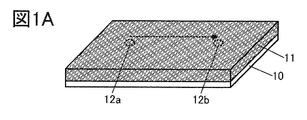
- FIG. 1A is a schematic diagram of a metal oxide film.
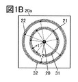
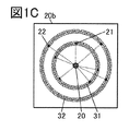
- 1B and 1C are schematic views of electron beam diffraction patterns.
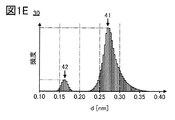
- 1D and 1E are schematic diagrams of histograms.
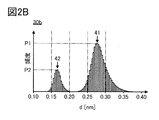
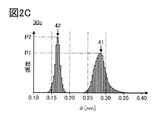
- 2A to 2C are schematic diagrams of histograms.
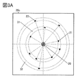
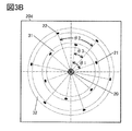
- 3A and 3B are schematic views of electron beam diffraction patterns.
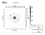
- FIG. 4A is an electron diffraction pattern.
- FIG. 4B is a histogram of lattice plane intervals.
- FIG. 5A is an electron diffraction pattern.
- FIG. 5B is a histogram of lattice plane intervals.
- FIG. 6A is an electron diffraction pattern.
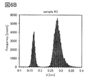
- FIG. 6B is a histogram of lattice plane intervals.
- FIG. 7A is an electron diffraction pattern.
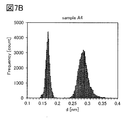
- FIG. 7B is a histogram of lattice plane intervals.
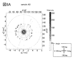
- FIG. 8A is an electron diffraction pattern.
- FIG. 8B is a histogram of lattice plane intervals.
- FIG. 9A is an electron diffraction pattern.
- FIG. 9B is a histogram of lattice plane intervals.
- FIG. 10 is a figure which shows the ratio of the frequency of an electron beam diffraction peak.
- FIG. 11A is a diagram showing a change in lattice plane spacing for each frame.
- FIG. 11B is a diagram showing a change in spot angle for each frame.
- FIG. 12A is a diagram showing a change in lattice plane spacing for each frame.
- FIG. 12B is a diagram showing a change in spot angle for each frame.
- FIG. 17 is a diagram showing angles of vertices of X-ray diffraction peaks.
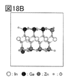
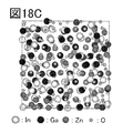
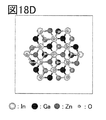
- 18A to 18E are diagrams showing a calculation model.
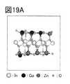
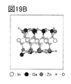
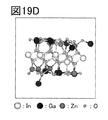
- 19A to 19E are diagrams showing calculation models.
- FIG. 20A is a diagram showing a relationship between temperature and average energy.
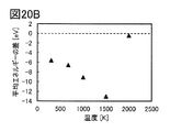
- FIG. 20B is a diagram showing the relationship between the temperature and the difference in average energy.
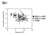
- FIG. 21 is a diagram for explaining the generation energy of defects.
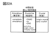
- FIG. 22A is a diagram illustrating classification of crystal structures of IGZO.
- FIG. 22B is a diagram illustrating an XRD spectrum of quartz glass.
- FIG. 22C is a diagram illustrating an XRD spectrum of crystalline IGZO.
- FIG. 22D is a diagram illustrating a microscopic electron beam diffraction pattern of crystalline IGZO.
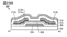
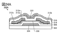
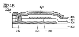
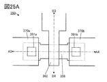
- FIG. 23A is a top view of the semiconductor device. 23B and 23C are cross-sectional views of the semiconductor device. 24A and 24B are cross-sectional views of the semiconductor device.
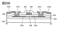
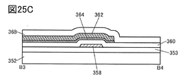
- FIG. 26A is a top view of the semiconductor device.
- 26B and 26C are cross-sectional views of the semiconductor device.
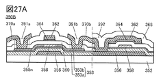
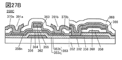
- 27A and 27B are cross-sectional views of the semiconductor device.
- 28A to 28C are diagrams illustrating a configuration example of a display device.
- FIG. 29 is a diagram showing a cross-sectional configuration example of a display device.
- FIG. 30 is a diagram showing a cross-sectional configuration example of a display device.
- FIG. 31 is a diagram showing a cross-sectional configuration example of a display device.
- FIG. 32A is a block diagram of a display device.
- 32B and 32C are circuit diagrams of the display device.
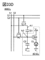
- 33A, 33C, and 33D are circuit diagrams of the display device.
- FIG. 33B is a timing chart.
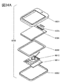
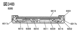
- 34A and 34B are configuration examples of the display module.
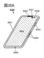
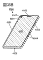
- 35A to 35C are diagrams illustrating configuration examples of electronic devices.
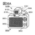
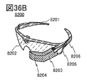
- 36A to 36E are diagrams illustrating configuration examples of electronic devices.
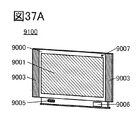
- 37A to 37G are diagrams illustrating configuration examples of electronic devices.
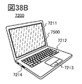
- 38A to 38D are diagrams illustrating configuration examples of electronic devices.
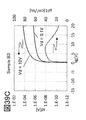
- 39A to 39D are diagrams illustrating Id-Vg characteristics of transistors.
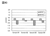
- FIG. 40 is a diagram showing a reliability evaluation result of a transistor.
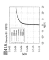
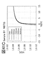
- 41A to 41D are diagrams showing Id-Vg characteristics of transistors.
- FIG. 42 is a HAADEF-STEM image and an EDX mapping image.
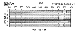
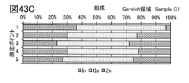
- 43A to 43D show the results of quantitative analysis of the composition of the metal oxide film.
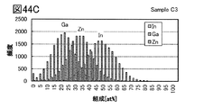
- 44A to 44C are histograms of the composition of the metal oxide film.
- a transistor is a type of semiconductor device that can realize amplification of current and voltage, switching operation that controls conduction or non-conduction, and so on.
- the transistors in this specification include IGFETs (Insulated Gate Field Effect Transistors) and thin film transistors (TFTs: Thin Film Transistors).
- source and drain may be switched when adopting transistors of different polarities or when the direction of current changes during circuit operation. Therefore, in this specification, the terms “source” and “drain” can be interchanged.
- film and “layer” can be interchanged with each other.
- conductive layer and “insulating layer” may be interchangeable with the terms “conductive film” and “insulating film”.
- a display panel which is one mode of a display device, has a function of displaying (outputting) an image or the like on a display surface. Therefore, the display panel is one mode of the output device.
- a connector of a FPC (Flexible Printed Circuit) or TCP (Tape Carrier Package) is attached to the substrate of the display panel, or an IC is mounted on the substrate by a COG (Chip On Glass) method or the like.
- a module in which is mounted is called a display panel module, a display module, or simply a display panel.
- a touch panel which is one mode of a display device has a function of displaying an image or the like on a display surface, a touch surface of a detected object such as a finger or a stylus, pressing, or approaching the display surface. And a function as a touch sensor for detecting. Therefore, the touch panel is an aspect of the input/output device.
- the touch panel can also be called, for example, a display panel (or display device) with a touch sensor or a display panel (or display device) with a touch sensor function.
- the touch panel can also be configured to have a display panel and a touch sensor panel. Alternatively, the inside or the surface of the display panel may have a function as a touch sensor.
- a touch panel substrate on which a connector or an IC is mounted may be referred to as a touch panel module, a display module, or simply a touch panel.
- FIG. 1A shows a schematic view of the metal oxide film 11 formed on the substrate 10.
- the metal oxide film 11 of one embodiment of the present invention is an oxide film containing indium, M (M is aluminum, gallium, yttrium, or tin) and zinc. Such an oxide film has a characteristic of showing semiconductor characteristics.
- the metal oxide film 11 is preferably a film formed by a sputtering method. In particular, it is preferable to use a polycrystalline metal oxide target as the sputtering target.
- the metal oxide film 11 includes a plurality of extremely fine (several nm or less) crystalline regions that are randomly oriented (also referred to as having no orientation).
- the metal oxide film 11 having such crystallinity has extremely high reliability as compared with the amorphous metal oxide film.
- the metal oxide film 11 may be a film in which crystal regions having no orientation and crystal regions having orientation are mixed.
- the metal oxide film 11 of one embodiment of the present invention can be applied to a semiconductor device.
- it can be applied to a semiconductor in which a channel of a transistor is formed.
- the metal oxide film 11 is particularly preferably an oxide film containing indium, gallium, and zinc. Further, as the metal oxide film 11, it is preferable to use a material having a high indium content ratio among the metal elements contained in the metal oxide film 11. In particular, it is preferable to use a material having a higher indium content than the gallium content. By applying such a metal oxide film 11 to a semiconductor layer of a transistor, a transistor with high field-effect mobility can be realized.
- the crystallinity of the metal oxide film 11 can be controlled by changing the film forming conditions.
- a film with high crystallinity can be obtained by increasing the proportion of oxygen gas in the deposition gas (also referred to as an oxygen flow rate ratio).
- a film with low crystallinity can be obtained by reducing the proportion of oxygen gas in the film formation gas or forming a film using a film formation gas containing no oxygen gas.
- a film with higher crystallinity can be formed as the substrate temperature during film formation is increased, and a film with low crystallinity can be obtained by forming the film with a lower substrate temperature or without heating the substrate. can do.
- the lower the crystallinity the higher the field effect mobility when applied to a transistor.
- the metal oxide film 11 of one embodiment of the present invention is a film having the following features in an electron beam diffraction pattern obtained by irradiating an electron beam from a direction perpendicular to the film surface.
- NBED Nano Beam Electron Diffraction
- SAED selected area electron beam diffraction
- the electron beam diffraction pattern was measured under the condition that the beam diameter of the electron beam was extremely small (for example, 0.3 nm or more and 10 nm or less or 5 nm or less). A plurality of spots that are discretely distributed in the direction (also referred to as the ⁇ direction) are confirmed. On the other hand, in the electron beam diffraction pattern under the condition that the beam diameter is large (for example, 50 nm or more, or 100 nm or more), a ring-shaped (also referred to as annular) pattern is observed.
- FIG. 1B and 1C are schematic diagrams of electron beam diffraction patterns obtained by irradiating an electron beam having a beam diameter of several nm from a direction perpendicular to the film surface of the metal oxide film 11.
- An electron beam diffraction pattern 20a shown in FIG. 1B is an electron beam diffraction pattern in a region 12a shown in FIG. 1A
- an electron beam diffraction pattern 20b shown in FIG. 1C is an electron beam diffraction pattern in a region 12b different from the region 12a. ..
- a spot (direct spot 20) of the incident electron beam that has passed through the sample and a first spot 21 on the side close to the direct spot 20 are provided.
- the second spot 22 is observed on the side farther from the direct spot 20 than the first spot 21.
- the first spot 21 is observed in the annular first region 31 where the radial distance r from the direct spot 20 is located at or near the distance r1.
- the second spot 22 is observed in the annular second region 32 where the radial distance r from the direct spot 20 is located at the distance r2 and its vicinity.
- the second region 32 is located outside the first region 31. That is, the distance r2 is larger than the distance r1.
- the electron beam irradiation position is scanned in parallel with the film surface direction of the metal oxide film 11 and the electron beam diffraction pattern of a region (region 12b) different from the region 12a is observed.
- the first spots 21 are observed at different positions within the first region 31, and the second spots 22 are observed at different positions within the second region 32.
- the metal oxide film 11 contains extremely minute crystal regions. Further, since the positions of the first spot 21 and the second spot 22 are different in different regions, it is found that the minute crystal regions included in the metal oxide film 11 do not have orientation.
- a plurality of electron beam diffraction patterns can be observed by measuring the irradiation position of the electron beam while scanning it in parallel with the film surface direction of the metal oxide film 11.
- Information such as the positions of the first spot 21 and the second spot 22 and the detection intensity can be obtained from each of the thus obtained electron beam diffraction patterns.
- the position information of the first spot 21 and the second spot 22 includes a distance r from the direct spot 20 and an angle ⁇ from an arbitrarily determined reference line.
- a histogram also referred to as a distribution chart or a frequency distribution chart
- the distance r, the angle ⁇ , the detected intensity, etc. can be obtained from the information obtained from the plurality of electron beam diffraction patterns.
- a method for evaluating a metal oxide film of one embodiment of the present invention will be described.
- an electron beam having a beam diameter of 0.3 nm or more and 10 nm or less is irradiated to a plurality of regions of the metal oxide film from a direction perpendicular to the film surface of the metal oxide film to obtain a plurality of electron beam diffraction patterns.
- the interplanar spacing d is calculated for the plurality of spots observed in the plurality of acquired electron beam diffraction patterns.
- the crystallinity of the metal oxide film can be evaluated from the calculated shape of the frequency distribution of the interplanar spacing d.
- the angle ⁇ from the reference line is calculated for a plurality of spots observed in a plurality of electron beam diffraction patterns obtained in the same manner, and the crystallinity of the metal oxide film is determined from the distribution shape of the angle ⁇ . Can be evaluated.
- the crystallinity of the metal oxide film can be evaluated from the information (for example, the shape of distribution) of the brightness (detection intensity) of a plurality of spots observed in a plurality of electron beam patterns obtained in the same manner.
- FIG. 1D shows an example of a histogram 30r showing the number (frequency) of spots observed in the electron diffraction pattern of the metal oxide film 11 with respect to the distance r from the direct spot 20.
- the histogram 30r shows the peak of the first spot 21 in which the apex of the peak is located in the first region 31 and the second spot having the apex of the peak in the second region 32. There are 22 peaks each.
- the value of the surface spacing d (hereinafter referred to as d value) corresponding to the spot is calculated by the following mathematical expression (1) using the distance r from the center of the direct spot to the target spot. be able to.
- L is the camera distance
- ⁇ is the wavelength of the electron beam.
- 1E shows a histogram 30 created using the d value calculated in this way.
- the histogram of the d value obtained from the electron beam diffraction pattern of the metal oxide film 11 of one embodiment of the present invention has two peaks (from the side with the larger d value, the first peak 41, the first peak 41, It has two peaks 42).
- the shape of the frequency distribution of the d value is such that the apex of the first peak 41 is located in the range where the d value is 0.25 nm or more and 0.30 nm or less, and the d value Is preferably a film in which the apex of the second peak 42 is located in the range of 0.15 nm or more and 0.20 nm or less.
- the plurality of first spots 21 forming the first peak 41 include spots due to scattered electrons derived from the medium-range ordered structure of minute crystalline clusters included in the metal oxide film 11. Since the first spot 21 contains scattered electrons due to diffraction having different plane spacing in the crystalline cluster, scattered electrons from crystalline clusters having different structures, etc., the scattering angle varies, and as a result, the first spot 21 The width of the region where the d value of the spot 21 can be observed becomes large. Therefore, the full width at half maximum of the first peak 41 tends to be larger than the full width at half maximum of the second peak 42.
- the first spot 21 may include a spot due to diffracted electrons diffracted by the minute crystal region included in the metal oxide film 11.
- the plurality of second spots 22 forming the second peak 42 are spots due to diffracted electrons diffracted by the minute crystal regions included in the metal oxide film 11.
- the second spot 22 is presumed to be derived from the diffracted electrons by the (110) plane and the crystal plane equivalent thereto.
- the shapes and heights of the first peak 41 and the second peak 42 included in the histogram 30 are shapes that reflect the crystallinity of the metal oxide film 11. Therefore, the crystallinity of the metal oxide film 11 can be evaluated from the shape of the frequency distribution of the histogram 30.
- histograms 30 of metal oxide films 11 having different crystallinities are shown in FIGS. 2A, 2B, and 2C, respectively.
- the histogram 30a shown in FIG. 2A is an example of the metal oxide film 11 having low crystallinity.
- a peak value P1 that is the value of the apex of the first peak 41 and a peak value P2 that is the value of the apex of the second peak 42 are shown.
- the heights and positions of the peak value P1 and the peak value P2 change according to the division width (class width) of the data of the histogram 30a, so the class width can be set to an appropriate width.
- the number of classes is preferably about the square root of the total number of data.
- the peak value P2 of the second peak 42 is lower than the peak value P1 of the first peak 41. Further, in the metal oxide film 11 having a crystallinity lower than that, the second peak 42 may be hardly observed in some cases.
- the histogram 30b shown in FIG. 2B is an example of the metal oxide film 11 having higher crystallinity than that of FIG. 2A.
- the number of the second spots 22 derived from the diffracted electrons increases, and the peak value P2 of the second peak 42 becomes higher than that in FIG. 2A.
- the number of first spots 21 decreases and the peak value P1 of the first peak 41 decreases due to the decrease in the proportion of the low-order region in the metal oxide film 11.
- the difference between the peak value P1 of the first peak 41 and the peak value P2 of the second peak 42 is smaller than that in FIG. 2A.
- the histogram 30c shown in FIG. 2C is an example of the metal oxide film 11 having higher crystallinity than that of FIG. 2B. As the crystallinity improves, the number of the second spots 22 further increases and the number of the first spots 21 decreases, so that the peak value P1 of the first peak 41 and the peak of the second peak 42. The magnitude relationship with the value P2 is reversed, and the peak value P2 is larger than the peak value P1.
- the crystallinity of the metal oxide film 11 can be evaluated from the shape of the frequency distribution of the histogram. Further, the crystallinity of the metal oxide films 11 formed under different film forming conditions can be compared by comparing the shapes of the frequency distributions of the histograms.
- the metal oxide film 11 may be a film in which a region having low crystallinity and a region having high crystallinity are mixed.
- the electron beam diffraction pattern is measured on the metal oxide film 11 while scanning the electron beam parallel to the film surface direction as described above, the electron beam derived from the region with low crystallinity is obtained.
- the diffraction pattern and the electron beam diffraction pattern derived from the highly crystalline region may appear alternately.
- FIG. 3A shows an example of an electron beam diffraction pattern 20c when a region of the metal oxide film 11 having low crystallinity is measured.
- first spots 21 are observed in the first region 31.
- the position of the first spot 21 in the radial direction (specifically, the distance from the direct spot 20 to the first spot 21) varies.
- the detection intensity of the first spot 21 also varies.
- the second spot 22 is observed in the second region 32.
- the variation of the second spot 22 in the radial direction is smaller than that of the first spot 21.
- the observed number of the second spots 22 is smaller than that of the first spots 21 in many cases. Further, the detection intensity may be relatively small.
- FIG. 3B shows an example of an electron beam diffraction pattern 20d when a highly crystalline region of the metal oxide film 11 is measured.
- first spots 21 are observed in the first region 31.
- An angle ⁇ 1 formed by two adjacent first spots 21 about the direct spot 20 is approximately 60 degrees. That is, the six first spots 21 are observed so as to satisfy the six-fold symmetry with the direct spot 20 as the center. Further, the radial position of the first spot 21 and the detected intensity have less variation as compared with the electron beam diffraction pattern 20c.
- the electron beam diffraction pattern 20d six second spots 22 are observed in the second region 32. Similarly to the first spot 21, the second spot 22 is also observed so as to satisfy the six-fold symmetry, and the angle ⁇ 2 formed by two adjacent second spots 22 is approximately 60 degrees.
- the angle ⁇ 3 formed by the first spot 21 and the second spot 22 centering on the direct spot 20 is approximately 30 degrees. From this, it can be seen that the highly crystalline region of the metal oxide film 11 has 6-fold symmetry with respect to the axis perpendicular to the film surface.
- the first spot 21 is derived from the diffracted electrons by the (100) plane and the crystal plane equivalent thereto. Inferred.
- the crystal region has the same crystal structure as the InGaZnO 4 crystal, the (100) plane satisfies the annihilation law, and theoretically no diffracted electron is observed.
- the annihilation rule is violated due to the fact that the entire crystal region is not a perfect crystal and is in an imperfect state including lattice strain, and therefore it is not originally observed. Diffracted electrons from the supposed (100) plane may be observed.
- the electron beam diffraction pattern 20d obtained by irradiating the electron beam perpendicularly to the film surface is 6 Since it has the rotational symmetry, it can be inferred that the c-axis is oriented in the film thickness direction as the crystal orientation of the crystal region included in the metal oxide film 11.
- the metal oxide film of one embodiment of the present invention can be formed by a sputtering method with or without heating the substrate.
- the substrate temperature may be room temperature or higher and 250° C. or lower, preferably room temperature or higher and 200° C. or lower, and more preferably room temperature or higher and 140° C. or lower.
- the substrate temperature is room temperature or higher and lower than 140° C. because productivity is high.
- the substrate temperature will be at or near room temperature in the initial state.
- the substrate may be heated by the energy given to the substrate by the sputtered particles or the like at the time of film formation.
- the device since a device for depositing a metal oxide film does not require a mechanism for heating a substrate, the device can be simplified and the cost can be reduced.
- the During film formation it may be in an atmosphere containing oxygen.
- the ratio of the flow rate of oxygen to the total flow rate of the film forming gas supplied to the film forming chamber of the film forming apparatus (hereinafter referred to as the oxygen flow ratio) is set to an appropriate value in the range of 0% to 100% You can By adjusting the oxygen flow rate, the crystallinity of the formed metal oxide film can be controlled. Specifically, the higher the oxygen flow rate ratio, the higher the crystallinity of the metal oxide film, and the lower the oxygen flow rate ratio, the lower the crystallinity of the metal oxide film.
- a rare gas such as argon can be used as the gas other than oxygen contained in the film forming gas.
- oxygen vacancies in the metal oxide film can be reduced.
- the atmosphere may not include oxygen.
- an oxide target that can be used for forming a metal oxide film for example, an In-M-Zn-based oxide (M is Al, Ga, Y, or Sn) can be used.
- M is Al, Ga, Y, or Sn
- an In-M-based oxide, an In-Zn-based oxide, or the like can be used as an oxide target that can be used for forming the metal oxide film.
- In-Ga oxide is particularly preferable because it is less likely to form oxygen vacancies.
- the metal oxide contained in the oxide target preferably has a high In content ratio.
- a metal oxide target having an In content of 33% or more and 60% or less, preferably 40% or more and 50% or less is used. It is preferable to use.
- the formed metal oxide film can be a metal oxide film having a high In content ratio.
- the composition of the formed metal oxide film and the composition of the oxide target may not necessarily match.
- the formed metal oxide film tends to have a lower Zn content than the oxide target.
- the metal oxide film can be formed as described above.
- the method for forming the metal oxide film is not limited to the above.
- Other film forming methods include plasma chemical vapor deposition (PECVD) method, thermal CVD (Chemical Vapor Deposition) method, ALD (Atomic Layer Deposition) method, vacuum deposition method, pulse laser deposition (PLD) method, liquid phase method. (Spin coating method, spraying method, etc.) may be used.
- PECVD plasma chemical vapor deposition
- thermal CVD Chemical Vapor Deposition
- ALD Atomic Layer Deposition
- PLD pulse laser deposition
- liquid phase method spin coating method, spraying method, etc.
- An example of the thermal CVD method is a MOCVD (Metal Organic Chemical Vapor Deposition) method.
- the crystallinity was evaluated by performing nanobeam electron diffraction analysis and X-ray diffraction (XRD: X-Ray Diffraction) analysis on metal oxide films having different fabrication methods.
- XRD X-ray diffraction
- samples (sample A1 to sample A6) in which a metal oxide film having a thickness of 40 nm was formed on a silicon wafer were used.
- In-Ga-Zn oxide was used as the metal oxide film, and the film forming conditions of the metal oxide film were varied among the samples.
- Table 1 shows film forming conditions for the metal oxide films of sample A1 to sample A6. Note that in Table 1, the substrate temperature at the time of forming the metal oxide film is Tsub, the oxygen flow rate ratio is O 2 /(Ar+O 2 ), the pressure is Pressure, and the power supply power is Power.
- the substrate temperature during deposition of the metal oxide film was room temperature (hereinafter, also referred to as RT).
- RT room temperature
- a mixed gas of oxygen gas and argon gas was used as a film forming gas, and the oxygen flow rate ratio was set to 10%.
- the pressure during film formation was 0.6 Pa, and the power supply power was 2.5 kW.
- the substrate temperature at the time of forming the metal oxide film was room temperature (RT).
- RT room temperature
- a mixed gas of oxygen gas and argon gas was used as a film forming gas, and the oxygen flow rate ratio was set to 30%.
- the pressure during film formation was 0.6 Pa, and the power supply power was 2.5 kW.
- the substrate temperature during deposition of the metal oxide film was room temperature (RT).
- RT room temperature
- a mixed gas of oxygen gas and argon gas was used as a film forming gas, and the oxygen flow rate ratio was set to 40%.
- the pressure during film formation was 0.6 Pa, and the power supply power was 2.5 kW.
- the substrate temperature at the time of forming the metal oxide film was room temperature (RT).
- RT room temperature
- a mixed gas of oxygen gas and argon gas was used as a film forming gas, and the oxygen flow rate ratio was set to 50%.
- the pressure during film formation was 0.6 Pa, and the power supply power was 2.5 kW.
- the substrate temperature during the formation of the metal oxide film was 100°C.
- a mixed gas of oxygen gas and argon gas was used as a film forming gas, and the oxygen flow rate ratio was set to 10%.
- the pressure during film formation was 0.6 Pa, and the power supply power was 2.5 kW.
- the substrate temperature during the formation of the metal oxide film was 100°C.
- a mixed gas of oxygen gas and argon gas was used as a film forming gas, and the oxygen flow rate ratio was set to 30%.
- the pressure during film formation was 0.6 Pa, and the power supply power was 2.5 kW.
- sample A1 to sample A6 were thinned in a direction parallel to the surface on which the metal oxide film was formed, and the thickness thereof was set to about 20 nm to 30 nm.
- the sample after thinning includes the surface of the metal oxide film when the metal oxide film was formed.
- an electron beam having an accelerating voltage of 200 kV (wavelength: about 2.51 pm) and a beam diameter of 1 nm was made incident from a direction perpendicular to the surface on which the metal oxide film was formed, to obtain a plurality of electron beam diffraction patterns. ..
- a plurality of electron beam diffraction patterns were obtained by photographing the electron beam diffraction pattern as a moving image while moving the electron beam irradiation location. The moving image was photographed while moving the electron beam irradiation spot by about 0.08 nm to 0.10 nm per frame, and about 3700 frames were obtained for each sample.
- An imaging plate of 200 pixels ⁇ 200 pixels was used for photographing the electron beam diffraction pattern.
- the magnitude (q) of the scattering vector for one pixel was 0.082426/nm/pixel.
- FIGS. 4A and 4B The results of nanobeam electron diffraction of sample A1 are shown in FIGS. 4A and 4B.
- the nanobeam electron diffraction results of sample A2 are shown in FIGS. 5A and 5B.
- the nanobeam electron diffraction results of sample A3 are shown in FIGS. 6A and 6B.
- Nanobeam electron diffraction results of sample A4 are shown in FIGS. 7A and 7B.
- the nanobeam electron diffraction results of sample A5 are shown in FIGS. 8A and 8B.
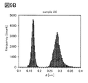
- the nanobeam electron diffraction results of sample A6 are shown in FIGS. 9A and 9B.
- FIG. 4A, FIG. 5A, FIG. 6A, FIG. 7A, FIG. 8A, and FIG. 9A show the electron beam diffraction pattern of the final frame in the moving image of each sample.
- the horizontal axis on the upper side and the vertical axis on the right side show the coordinates (denoted as pixel) of the pixels of the imaging plate with the lower left side as a reference.
- the magnitude of the scattering vector (q [/nm]) is shown on the lower horizontal axis and the left vertical axis.
- each point shown in each drawing is shown in a darker color as the intensity of the spot (detection intensity (Intensity)) is higher, and in a lighter color as the intensity is lower.
- the position and intensity values of each spot were obtained.
- the region of 30 pixels from the center and the region of 90 pixels from the center are indicated by solid circles.
- the lattice spacing (d) corresponds to 0.13348 nm or more and 0.4044 nm or less.
- spots having a spot intensity (0 to 255) of 64 or more and an area of 2 pixels or more were evaluated.
- the center of the electron beam diffraction pattern and each spot are connected by a solid line.
- the center of the electron beam diffraction pattern was the center of the spot (also referred to as a direct spot) of the incident electron beam that passed through the sample without being diffracted.
- FIG. 4B, FIG. 5B, FIG. 6B, FIG. 7B, FIG. 8B, and FIG. 9B are histograms (frequency distribution charts) of the lattice spacing (d) in all frames of the moving image acquired for each sample.
- the horizontal axis represents the lattice spacing (d [nm])
- the vertical axis represents the frequency (Frequency [count]).
- the lattice spacing (d) has an apex in the range of 0.25 nm to 0.30 nm. It has a peak (first peak) and a peak (second peak) having an apex in the range of 0.15 nm to 0.20 nm.
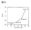
- FIG. 10 shows the ratio (P2/P1) of the peak value (peak value P2) of the second peak to the peak value (peak value P1) of the first peak for sample A1 to sample A4. Show.
- the horizontal axis represents the oxygen flow rate ratio (O 2 /(Ar+O 2 )[%]) when forming the metal oxide film, and the vertical axis represents the ratio of the peak value P2 to the peak value P1 (P2/ P1) is shown.
- the second peak tends to increase as the oxygen flow rate ratio increases. Further, in sample A1 to sample A3, the value at the apex of the first peak (peak value P1) is higher than the value at the apex of the second peak (peak value P2). On the other hand, in sample A4 with the highest oxygen flow ratio, these magnitude relationships are reversed, and the value of the peak of the second peak (peak value P2) is the value of the peak of the first peak (peak value P1).
- the value of P2/P1 shown in FIG. 10 is also a value exceeding 1.
- sample A5 comparing sample A5 and sample A6, in sample A5 where the oxygen flow ratio is low, the peak value of the first peak is higher than the peak value of the second peak, while the oxygen flow ratio is higher. In sample A6 with high conditions, the value of the apex of the second peak exceeds the value of the apex of the first peak. From this, it can be confirmed that the higher the oxygen flow rate ratio, the higher the crystallinity.
- sample A5 has a larger second peak.
- sample A2 and sample A6 have a larger second peak. From this, it can be confirmed that the crystallinity improves as the substrate temperature during film formation increases even under the same oxygen flow rate condition.
- the evaluation method of one embodiment of the present invention it is possible to obtain information about the crystallinity of the metal oxide film not only from the histogram but also from data for each frame regarding the position and brightness of the detected spot.
- FIG. 11A shows a change in the lattice spacing (d) for each frame of sample A1.
- the horizontal axis represents the frame number (Frame No.)
- the vertical axis represents the lattice plane spacing (d [nm]).
- each point shown in FIG. 11A is indicated by a darker color as the intensity (Intensity) of the spot is higher and a lighter color as the intensity is lower.
- FIG. 11B shows changes in the spot angle (Angle) for each frame of the sample A1.
- the horizontal axis indicates the frame number (Frame No.)
- the vertical axis indicates the angle of the spot (Angle [°]).
- each point shown in FIG. 11B is shown in a darker color as the intensity (intensity) of the spot is higher, and in a lighter color as the intensity is lower.
- the first spot is in the region where the lattice spacing (d) is 0.25 nm to 0.35 nm
- the second spot is in the region where it is 0.15 nm to 0.20 nm.
- the first spot is continuously observed regardless of the measurement position, whereas the second spot is discretely observed.
- the position where the second spot is observed is presumed to be a region having relatively higher crystallinity than other positions. From this, it can be confirmed that the metal oxide film does not have uniform crystallinity, but a region having relatively high crystallinity and a region having relatively low crystallinity are mixed.
- sample A1 has almost no angle dependence of the spot. From this, it is assumed that most of the crystal regions contained in sample A1 have no orientation and are randomly oriented.
- FIG. 12A shows a change in the lattice plane spacing (d) for each frame of sample A6, and FIG. 12B shows a change in the spot angle (Angle) for each frame.
- the second spots in the region where the lattice spacing (d) is 0.15 nm to 0.20 nm are continuously observed regardless of the position (frame), so compared to sample A1. It can be confirmed that sample A6 has extremely high crystallinity. Focusing on the first spots in the region where the lattice spacing (d) is 0.25 nm to 0.35 nm, a region with a small variation (for example, a range from 0 frame to 200 frames) and a region with a large variation ( It can be confirmed that, for example, a range of 300 to 500 frames) appears alternately. Further, in the region where the variation of the first spot is small, the variation of the second spot tends to be small. From this, it can be inferred that a large-sized crystal region exists in the metal oxide film.
- the spots are discretely observed at intervals of about 30 degrees in the region where the variation of the first spot is small in FIG. 12A.
- FIG. 9A six first spots and six second spots outside the first spot are observed so as to be located at the vertices of a regular hexagon, and electrons having six-fold symmetry are observed. It can be seen that it shows a line diffraction pattern. From this, it can be inferred that a single crystal region having six-fold symmetry is observed in the region where the first spot variation in FIGS. 12A and 12B is small.
- the crystallinity of the metal oxide film can be accurately evaluated and compared.
- the GIXRD (Grazing-Incidence XRD) method which is a type of the out-of-plane method, was used.
- the GIXRD method is also referred to as a thin film method or a Seemann-Bohlin method.
- the GIXRD method is a method of fixing the incident angle of X-rays at a very shallow angle and changing the angle of a detector provided facing the X-ray source to measure the X-ray diffraction intensity. In this embodiment, the incident angle is 0.70 degrees.
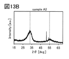
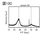
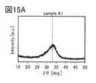
- FIGS. 13A to 13C The XRD measurement results of sample A1 to sample A3 are shown in FIGS. 13A to 13C.
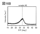
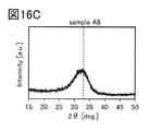
- 14A to 14C show the XRD measurement results of sample A4 to sample A6.
- the horizontal axis represents 2 ⁇ and the vertical axis represents intensity.
- the angle (2 ⁇ ) of the apex of the diffraction peak was calculated using Lorentz function fitting. The least squares method was used for fitting the Lorentz function. Enlarged views of FIGS. 13A, 13B, and 13C are shown in FIGS. 15A, 15B, and 15C. Further, enlarged views of FIGS. 14A, 14B and 14C are shown in FIGS. 16A, 16B and 16C. The angle (2 ⁇ ) of the peak of the diffraction peak in each sample is shown in FIG. In FIG.
- the horizontal axis represents the oxygen flow rate ratio (O 2 /(Ar+O 2 )[%]) at the time of forming the metal oxide film, and the vertical axis represents the angle of the apex of the diffraction peak (2 ⁇ [deg.]).
- calculation model 1A is a calculation model having a crystal region, and is a calculation model imitating an nc film.
- calculation model 2A is a calculation model having no crystal region and is a calculation model imitating an amorphous film. The crystal region will be described later.
- the crystal region is placed at the center of the calculation model. Note that the number of atoms arranged in the crystal region is 87.
- the atoms located in the crystal region refer to 87 atoms arranged in the crystal region. Further, any one or more of the atoms located in the crystal region may move to the outer peripheral portion of the crystal region depending on the calculation performed later.
- a plurality of In atoms, a plurality of Ga atoms, a plurality of Zn atoms, and a plurality of O atoms are randomly arranged on the outer peripheral portion of the crystal region.
- the number of In atoms, the number of Ga atoms, the number of Zn atoms, and the number of O atoms, which are arranged in the outer peripheral portion, and the size of the outer peripheral portion are determined by the above-described crystal regions and the atoms arranged in the outer peripheral portion.
- the number of atoms arranged on the outer peripheral portion is 291. Therefore, the number of atoms included in the calculation model is 378. Further, any one or more of the atoms arranged in the outer peripheral portion may move to the crystal region depending on calculation performed later.
- the coordinates of the atoms located in the crystal region are fixed, and calculations for melting the outer periphery are performed.
- the temperature is set to 3500 K
- the time step width is set to 1 fs
- the number of steps is set to 6000 times.
- the calculation performed by setting the temperature, the time step size, and the number of steps may be referred to as first-principles molecular dynamics calculation or quantum molecular dynamics calculation.
- the potential generated by the Projector Augmented Wave (PAW) method was used as the electronic state pseudopotential, and GGA/PBE (Generalized-Gradient-Aproximation/Perdew-Burke-Ernzerhof) was used as the functional.
- PAW Projector Augmented Wave
- GGA/PBE Generalized-Gradient-Aproximation/Perdew-Burke-Ernzerhof
- the first-principles molecular dynamics calculation and the calculation (also referred to as optimization calculation) for optimizing the structure of the calculation model, which will be described later in this embodiment, In, Ga, and Zn are calculated. In the potential, the 3d state or the 4d state is not considered as the valence band. Further, the lattice vector (the length of the axis and the angle between the axes) of the calculation model is fixed. That is, the first-principles molecular dynamics calculation is performed under conditions (NVT ensemble) in which the number of particles (N), volume (V), and temperature (T) are constant. In the first principle molecular dynamics calculation, Nose-Hooverthermostat is used as a method for controlling the temperature.
- the cooling rate is 500 K/ps.
- the coordinates of atoms located in the crystal region are fixed, the time step width is set to 1 fs, the number of steps is set to 1000, and other calculation conditions are set to condition 1 shown in Table 2.
- the temperature is set to 3500 K and the first-principles molecular dynamics calculation is performed on the calculation model obtained by the calculation for melting the outer peripheral portion.
- the temperature is set to 3000 K and first-principles molecular dynamics calculation is performed on the calculation model obtained after the calculation.
- the first-principles molecular dynamics calculation is performed with the temperature set to 2500 K for the calculation model obtained after the calculation.
- the temperature is set to 2000 K for the calculation model obtained after the calculation, and first-principles molecular dynamics calculation is performed.
- a first-principles molecular dynamics calculation is performed with the temperature set to 1500 K for the calculation model obtained after the calculation.
- the temperature is set to 1000 K and first-principles molecular dynamics calculation is performed on the calculation model obtained after the calculation.
- the temperature is set to 500 K and first-principles molecular dynamics calculation is performed on the calculation model obtained after the calculation.
- the calculation condition is set to the condition 2 shown in Table 2, the coordinates of the atoms located in the crystal region are fixed to the calculation model obtained by the calculation for relaxing the structure of the outer peripheral portion, Perform calculations to optimize the structure. After that, in order to optimize the structure of the crystal region by fixing the coordinates of the atom located in the outer periphery and the coordinate of one In atom existing in the center of the crystal region with respect to the calculation model obtained after the calculation. Calculate. After that, with respect to the calculation model obtained after the calculation, only the In atom is fixed in coordinates, and calculation for optimizing the structure of the entire calculation model (crystal region and outer peripheral portion) is performed. After that, the calculation condition is set to the condition 3 shown in Table 2, and for the calculation model obtained after the calculation, only the In atom concerned has the fixed coordinates, and the calculation for optimizing the structure of the whole calculation model is performed. ..
- FIGS. 18A to 18D are diagrams showing an overall image of the calculation model 1A.
- 18B and 18D are diagrams showing the crystal region of the calculation model 1A.
- 18A and 18B are views seen from the side surface of the hexagonal columnar region, and
- FIGS. 18C and 18D are views seen from the upper surface of the hexagonal columnar region.
- the calculation for melting the crystal region and the outer peripheral portion of the calculation model 1A is performed. Specifically, the calculation model 1A was prepared, and the temperature was set to 3500 K, the time step width was set to 1 fs, the number of steps was set to 6000, and the other calculation conditions were set to Condition 1 shown in Table 2 without fixing the coordinates of all atoms. Set and perform first-principles molecular dynamics calculations.
- the cooling rate is 500 K/ps.
- the time step width is set to 1 fs
- the number of steps is set to 1000 times
- other calculation conditions are set to Condition 1 shown in Table 2 without fixing the coordinates of all atoms.
- the temperature is set to 3500 K and the first-principles molecular dynamics calculation is performed on the calculation model obtained by the calculation for melting the crystal region and the outer peripheral portion.
- the temperature is set to 3000 K and first-principles molecular dynamics calculation is performed on the calculation model obtained after the calculation.
- the first-principles molecular dynamics calculation is performed with the temperature set to 2500 K for the calculation model obtained after the calculation.
- the temperature is set to 2000 K for the calculation model obtained after the calculation, and first-principles molecular dynamics calculation is performed.
- a first-principles molecular dynamics calculation is performed with the temperature set to 1500 K for the calculation model obtained after the calculation.
- the temperature is set to 1000 K and first-principles molecular dynamics calculation is performed on the calculation model obtained after the calculation.
- the temperature is set to 500 K and first-principles molecular dynamics calculation is performed on the calculation model obtained after the calculation.
- the first-principles molecular dynamics calculation is performed by setting the calculation condition of 1 to the condition 1 shown in Table 2.
- the calculation condition is set to the condition 2 shown in Table 2, and the structure of the whole calculation model is set without fixing the coordinates of all atoms to the calculation model obtained by the calculation for relaxing the whole calculation model. Perform calculations to optimize.
- the calculation condition is set to the condition 3 shown in Table 2, and calculation for optimizing the structure of the whole calculation model is performed on the calculation model obtained after the calculation without fixing the coordinates of all atoms. ..
- the total energy was calculated and compared for each of the calculation model 1A and the calculation model 2A created by the above method.
- the calculation condition is set to the condition 3 shown in Table 2, and for the calculation model 1A, the coordinates of only one In atom existing in the center of the crystal region are fixed and one-point calculation is performed.
- the calculation model 2A one-point calculation is performed without fixing the coordinates of all atoms. The total energy calculated by the calculation is compared.
- the total energy value of calculation model 1A was smaller than the total energy value of calculation model 2A, specifically, 6.83 eV. Therefore, it can be seen that the calculation model 1A having the crystal region is more stable than the calculation model 2A having no crystal region. That is, it is suggested that the nc film is stabilized by having the crystal region.
- the structure of the calculation model 3A is a single crystal structure.
- the k-point grid is set to 2 ⁇ 2 ⁇ 3, the other calculation conditions are set to Condition 3 shown in Table 2, and one-point calculation is performed.
- the total energy value of the calculation model of the single crystal structure was smaller than the total energy value of the calculation model 1A, specifically, 54.88 eV. That is, it can be seen that the crystallinity in the film is improved and the film is energetically stable.
- the calculation model 1A has higher energy than the calculation model of the single crystal structure, it is more stable than the calculation model 2A, and therefore the existence of the crystal region contributes to the stabilization of the nc film. It is suggested.
- thermal stability of nc film will be described using the results of the first principle calculation.
- the thermal stability of the nc film is evaluated using the internal energy described later.
- the internal energy U is calculated using the following formula.
- M I is the mass of the I-th (I is a natural number) nucleus
- m is the mass of the electron
- v I is the velocity of the I-th nucleus. That is, the first term on the right side of the above equation represents the kinetic energy of the nucleus, and the third term on the right side of the above equation represents the kinetic energy of the electron.
- Z I is the charge of the I-th atomic nucleus
- e is the charge of the electron.
- r IJ is a distance between the I-th nucleus and the J-th nucleus (J is an integer larger than I)
- r ij is the i-th electron (i is a natural number).
- the j-th (j is an integer larger than i) electron. That is, the second term on the right side of the above formula is the potential energy related to the interaction between nuclei and nuclei, and the fourth term on the right side of the above formula is the potential energy related to the interaction between electrons and the right side of the above formula.
- the fifth term of is the potential energy related to the interaction between the nucleus and the electron.
- the internal energy U is calculated as the sum of kinetic energy and potential energy.
- the internal energy U is used to verify thermodynamic phase stability in this specification.
- First-principles molecular dynamics calculations are performed by setting the temperature to 300K, 673K, 1000K, 1500K, or 2000K for each of the above-mentioned calculation model 1A and calculation model 2A.
- the calculation model 1A the coordinate of one In atom existing in the center of the crystal region is fixed and the first principle molecular dynamics calculation is performed.
- the calculation model 2A the first-principles molecular dynamics calculation is performed without fixing the coordinates of all atoms.
- the time step width is set to 1 fs
- the number of steps is set to 10,000 times
- other calculation conditions are set to the condition 2 shown in Table 2.
- Figure 20A shows the relationship between temperature and average energy calculated by the above method.
- the horizontal axis represents temperature [K] and the vertical axis represents average energy [eV].
- 20A is a plot of average energy when the calculation model 1A is used, and a white square plot is a plot of average energy when the calculation model 2A is used.
- the calculation conditions are shown in Table 2 for each of the calculation models (a total of 5 types) obtained by performing the first principle molecular dynamics calculation by setting each temperature for the calculation model 1A. Set to 2 and perform calculations to optimize the structure of the calculation model. Note that the optimization calculation is performed by fixing the coordinates of one In atom existing in the center of the crystal region. Then, for each of the calculation models (a total of 5 types) obtained by performing the optimization calculation, the calculation condition is set to the condition 3 shown in Table 2 to optimize the structure of the calculation model. I do.
- FIGS. 19A to 19E A part of the calculation model (total of 5 types) obtained by the above calculation is shown in FIGS. 19A to 19E.
- 19A to 19E show an array of 87 atoms arranged in the crystal region in the calculation model before the atoms are arranged in the outer peripheral portion of the crystal region.
- FIG. 19A is a calculation model obtained by performing the first-principles molecular dynamics calculation in which the temperature is set to 300K and the optimization calculation
- FIG. 19B is the first-principles molecular dynamics in which the temperature is set to 673K.
- FIG. 19C is a calculation model obtained by performing the dynamics calculation and the optimization calculation
- FIG. 19C shows the calculation model obtained by performing the first principle molecular dynamics calculation in which the temperature is set to 1000K and the optimization calculation.
- FIG. 19D is a calculation model obtained by performing the first principle molecular dynamics calculation in which the temperature is set to 1500K and the optimization calculation
- FIG. 19E is the first principle in which the temperature is set to 2000K. It is a calculation model obtained by performing molecular dynamics calculation and optimization calculation.
- the difference between the average energy of calculation model 1A and the average energy of calculation model 2A is calculated at each temperature, and the thermal stability of calculation model 1A and calculation model 2A is compared. Note that the relationship between the temperature and the average energy of the calculation model 1A and the calculation model 2A is as shown in FIG. 20A.
- FIG. 20B shows the relationship between the temperature and the value obtained by subtracting the average energy of calculation model 2A from the average energy of calculation model 1A (also called the difference in average energy).
- the horizontal axis represents temperature [K]
- the vertical axis represents difference in average energy [eV].
- H 2 O may generate electrons serving as carriers. Therefore, when H 2 O is generated in the channel formation region in the oxide semiconductor, the electrical characteristics of the transistor are changed such that the transistor is likely to have normally-on characteristics. Therefore, it is preferable to suppress the generation of H 2 O in the channel formation region in the oxide semiconductor.
- the generation energy of defects is calculated using the following formula. It can be said that the smaller the generation energy of a defect, the easier the defect is generated.
- E form (defect) is a generation energy of a defect (defect)
- E (defect) is a total energy of a calculation model including one defect
- E (no defect) is a calculation model of the calculation model including no defect.
- the total energy the atom X is an atom increased or decreased by generating a defect
- ⁇ (X) is the chemical potential of the atom X
- n X is the number of increase or decrease of the atom X.
- the defect is H 2 O
- X is an oxygen atom (O) or a hydrogen atom (H)
- n O is ⁇ 1
- n H is +1.
- E(O 2 ) is the total energy of oxygen molecules (O 2 )
- E(H 2 O) is the total energy of water molecules (H 2 O).
- E(O 2 ) is a calculation for optimizing the structure of the O 2 molecule by arranging one O 2 molecule in the lattice of 1 nm 3 and setting the calculation condition to Condition 2 shown in Table 2. Then, the calculation is performed by performing one-point calculation on the calculation model obtained after the calculation. Further, E(H 2 O) optimizes the structure of the H 2 O molecule by arranging one H 2 O molecule in the lattice of 1 nm 3 and setting the calculation condition to the condition 2 shown in Table 2. Calculation is performed, and then one-point calculation is performed on the calculation model obtained after the calculation, to obtain the calculation.
- Calculation model 3A was prepared in order to calculate the generated energy of defects. Hereinafter, a method of creating the calculation model 3A will be described. The calculation conditions shown in Table 2 are used for the calculation for creating the calculation model 3A.
- the calculation model 1A First, prepare the calculation model 1A, and perform calculations to relax the structure of the outer periphery of the calculation model 1A. Specifically, the calculation model 1A is prepared, the coordinates of the atoms located in the crystal region are fixed, the temperature is 1000 K, the time step width is 1 fs, the number of steps is 10000 times, and other calculation conditions are shown in Table 2. The first principle molecular dynamics calculation is performed under the condition 2.
- the coordinates of the atoms located in the crystal region are fixed to the calculation model obtained by the calculation for relaxing the structure of the outer periphery, and the outer periphery is fixed. Perform calculations to optimize the structure of parts. After that, in order to optimize the structure of the crystal region by fixing the coordinates of the atom located in the outer periphery and the coordinate of one In atom existing in the center of the crystal region with respect to the calculation model obtained after the calculation. Calculate. Then, with respect to the calculation model obtained after the calculation, the coordinates of one In atom existing in the center of the crystal region are fixed, and a calculation for optimizing the structure of the entire calculation model is performed. After that, the calculation condition is set to the condition 3 shown in Table 2, and the coordinate of one In atom existing in the center of the crystal region is fixed to the calculation model obtained after the calculation to optimize the structure of the entire calculation model. Calculation to realize.
- the generation energy of H 2 O is calculated using the calculation model 3A created by the above method. Specifically, a calculation model including one H 2 O is prepared by replacing one oxygen atom in the calculation model 3A with one hydrogen atom. Since the number of oxygen atoms in the calculation model 3A is 216, 216 calculation models containing one H 2 O are prepared. The calculation model that does not include H 2 O is the calculation model 3A itself.
- the calculation condition is set to the condition 3 shown in Table 2, the calculation for optimizing the structure of the entire calculation model .
- E(defect) be the total energy of the calculation model containing one H 2 O obtained after the calculation
- E(no defect) be the total energy of the calculation model that does not contain H 2 O obtained after the calculation.
- H 2 O may be changed to another defect (for example, oxygen deficiency and hydrogen) by performing the calculation for a calculation model including one H 2 O.
- the generation energy of H 2 O is calculated by using E(defect) and E(no defect) calculated by the above method.
- the calculated H 2 O production energy is shown in FIG.
- the horizontal axis represents the distance (Distance) [ ⁇ ] from the In atom existing in the center of the crystal region to H 2 O arranged in the calculation model before performing the calculation for optimizing the structure of the calculation model as a whole.
- the vertical axis represents the H 2 O formation energy (Formation energy) [eV].
- a black square ( ⁇ ) plot shown in FIG. 21 represents H 2 O generation energy located in a region near In (a crystal core region) in the crystal region, and a white square (shown in FIG.
- the plot of ⁇ ) is the production energy of H 2 O located in the region other than the core region in the crystal region (also referred to as the crystal shell region), and the cross mark ( ⁇ ) shown in FIG. Energy of H 2 O located at the position.
- the number of oxygen located in the core region of the crystal is 12, and the number of oxygen located in the shell region of the crystal is 38.
- H O located in core area of the crystals the average value of H O, generates energy H O located on the outer peripheral portion positioned to shell region of the crystal, respectively, is 2.75 eV, 2.60EV, and 2.14eV It was
- the crystal region (core region of the crystal, and the crystal of the shell region) than in the outer peripheral portion larger variations in the formation energy of H O, that value is less H O generation energy H O often I understand. This is presumably because the bond length fluctuation is larger in the outer peripheral portion having lower crystallinity than in the crystal region, and there are more oxygen atoms having weaker bonding force with the metal atom.
- H 2 O is hard to be generated in the crystal region, and H 2 O is easily generated in the region having low crystallinity (the outer peripheral portion). Therefore, the presence of the crystalline region suppresses the generation of H 2 O. Therefore, by using the nc film for a transistor, variation in electric characteristics of the transistor can be suppressed.
- the oxide semiconductor (metal oxide) is classified into a single crystal oxide semiconductor and a non-single crystal oxide semiconductor other than the single crystal oxide semiconductor.
- the non-single-crystal oxide semiconductor include a CAAC-OS (c-axis aligned crystal oxide semiconductor), a polycrystalline oxide semiconductor, an nc-OS (nanocrystal oxide semiconductor), and a pseudo-amorphous oxide semiconductor (a-like oxide).
- OS amorphous-like oxide semiconductor (OS), amorphous oxide semiconductor, and the like.
- CAAC-OS has c-axis orientation, and has a crystal structure in which a plurality of nanocrystals are connected in the ab plane direction and have strain.
- the strain refers to a portion where the orientation of the lattice arrangement is changed between a region where the lattice arrangement is uniform and another region where the lattice arrangement is uniform in the region where a plurality of nanocrystals are connected.
- ⁇ Nanocrystals are basically hexagonal, but they are not limited to regular hexagons and may be non-regular hexagons.
- the strain may have a lattice arrangement such as a pentagon or a heptagon.
- a lattice arrangement such as a pentagon or a heptagon.
- the crystal structure in which a clear grain boundary is confirmed is called a so-called polycrystal.
- the crystal grain boundaries serve as recombination centers, and carriers are likely to be trapped to cause a decrease in on-state current of the transistor or a decrease in field-effect mobility. Therefore, the CAAC-OS in which clear crystal grain boundaries are not confirmed is one of crystalline oxides having a crystal structure suitable for a semiconductor layer of a transistor.
- a structure containing Zn is preferable for forming the CAAC-OS.
- In—Zn oxide and In—Ga—Zn oxide are preferable because they can suppress generation of crystal grain boundaries more than In oxide.
- the CAAC-OS is a layered crystal in which a layer containing indium and oxygen (hereinafter, an In layer) and a layer containing elements M, zinc, and oxygen (hereinafter, a (M,Zn) layer) are stacked. It tends to have a structure (also called a layered structure).
- indium and the element M can be replaced with each other, and when the element M of the (M,Zn) layer is replaced with indium, it can be expressed as an (In,M,Zn) layer. Further, when the indium in the In layer is replaced with the element M, it can be expressed as an (In,M) layer.
- CAAC-OS is a metal oxide with high crystallinity.
- the CAAC-OS since it is difficult to confirm a clear crystal grain boundary, it can be said that a decrease in electron mobility due to the crystal grain boundary does not easily occur.
- the crystallinity of a metal oxide may be lowered due to the mixture of impurities, the generation of defects, or the like; therefore, the CAAC-OS can be referred to as a metal oxide with few impurities and defects (such as oxygen vacancies). Therefore, the metal oxide having CAAC-OS has stable physical properties. Therefore, the metal oxide containing CAAC-OS is highly heat resistant and highly reliable.
- Nc-OS has a periodic atomic arrangement in a minute region (for example, a region of 1 nm or more and 10 nm or less, particularly a region of 1 nm or more and 3 nm or less). Moreover, in the nc-OS, no regularity is found in the crystal orientation between different nanocrystals. Therefore, the orientation is not seen in the entire film. Therefore, the nc-OS may be indistinguishable from the a-like OS or the amorphous oxide semiconductor depending on the analysis method.
- In-Ga-Zn oxide which is a kind of metal oxide containing indium, gallium, and zinc, may have a stable structure by using the above-described nanocrystal. is there.
- IGZO tends to have difficulty in crystal growth in the atmosphere, so that a smaller crystal (for example, the above-mentioned nanocrystal) is used than a large crystal (here, a crystal of several mm or a crystal of several cm).
- a smaller crystal for example, the above-mentioned nanocrystal
- a large crystal here, a crystal of several mm or a crystal of several cm.
- it may be structurally stable.
- the a-like OS is a metal oxide having a structure between the nc-OS and the amorphous oxide semiconductor.
- the a-like OS has a void or a low density region. That is, the crystallinity of the a-like OS is lower than that of the nc-OS and the CAAC-OS.
- Oxide semiconductors have various structures, and each has different characteristics.
- the oxide semiconductor of one embodiment of the present invention may include two or more of an amorphous oxide semiconductor, a polycrystalline oxide semiconductor, an a-like OS, an nc-OS, and a CAAC-OS.
- CAC-OS Cloud-Aligned Composite
- the CAC-OS relates to the material composition.
- the CAC-OS has a conductive function in a part of the material, an insulating function in a part of the material, and a semiconductor function in the whole material.
- a conductive function is a function of allowing electrons (or holes) serving as carriers to flow
- an insulating function is a function of not allowing electrons serving as carriers to flow. is there.
- the CAC-OS has a conductive area and an insulating area.
- the conductive region has the above-mentioned conductive function
- the insulating region has the above-mentioned insulating function.
- the conductive region and the insulating region may be separated at the nanoparticle level.
- the conductive region and the insulating region may be unevenly distributed in the material.
- the conductive region may be observed as the periphery is blurred and connected in a cloud shape.
- the conductive region and the insulating region may be dispersed in the material in a size of 0.5 nm or more and 10 nm or less, preferably 0.5 nm or more and 3 nm or less.
- CAC-OS is composed of components having different band gaps.
- the CAC-OS includes a component having a wide gap due to the insulating region and a component having a narrow gap due to the conductive region.
- the carrier when the carrier flows, the carrier mainly flows in the component having the narrow gap.
- the component having the narrow gap acts complementarily to the component having the wide gap, and the carrier also flows to the component having the wide gap in conjunction with the component having the narrow gap. Therefore, when the CAC-OS is used for a channel formation region of a transistor, a high current drivability, that is, a large on-current and a high field-effect mobility can be obtained when the transistor is on.
- the CAC-OS can also be referred to as a matrix composite material or a metal matrix composite material.
- oxide semiconductors may be classified differently from the above.
- classification of crystal structures in an oxide semiconductor is described with reference to FIG. 22A.
- 22A is a diagram illustrating classification of crystal structures of oxide semiconductors, typically IGZO (a metal oxide containing In, Ga, and Zn).
- IGZO is roughly classified into Amorphous (amorphous), Crystalline (crystalline), and Crystal (crystalline).
- Amorphous includes completely amorphous.
- CAAC, nc, and CAC are included in Crystalline. Note that the classification of Crystalline excludes single crystal, poly crystal, and complete amorphous. Moreover, single crystal and poly crystal are included in Crystal.
- the structure in the thick frame shown in FIG. 22A is an intermediate state between Amorphous (amorphous) and Crystal (crystal) and belongs to a new boundary region (New crystalline phase).
- the structure is in the boundary region between Amorphous and Crystal. That is, the structure can be restated as a completely different structure from an energetically unstable Amorphous (amorphous) and Crystal (crystal).
- FIGS. 22B and 22C X-ray diffraction spectra of quartz glass and IGZO having a crystal structure classified into Crystalline (also referred to as crystalline IGZO) are shown in FIGS. 22B and 22C.
- FIG. 22B is an XRD spectrum of quartz glass
- FIG. 22C is an XRD spectrum of crystalline IGZO.
- the thickness of the crystalline IGZO shown in FIG. 22C is 500 nm.
- the shape of the XRD spectrum peak of quartz glass is almost symmetrical.
- the peak shape of the XRD spectrum is bilaterally asymmetric.
- the fact that the peak shape of the XRD spectrum is asymmetrical indicates the existence of crystals. In other words, unless the peak shape of the XRD spectrum is bilaterally symmetric, it cannot be said to be Amorphous.
- the crystal structure of the film can be evaluated by a diffraction pattern (also referred to as a micro electron diffraction pattern) observed by a micro electron diffraction method (NBED: Nano Beam Electron Diffraction).
- the IGZO film formed at room temperature is in the crystalline state, the amorphous state, the intermediate state, or the amorphous state.
- FIG. 23A is a top view of the transistor 300
- FIG. 23B corresponds to a cross-sectional view taken along dashed-dotted line A1-A2 illustrated in FIG. 23A
- FIG. 23C is a cross-sectional view taken along dashed-dotted line B1-B2 illustrated in FIG. 23A. It corresponds to a sectional view of the surface.
- the one-dot chain line A1-A2 direction corresponds to the channel length direction
- the one-dot chain line B1-B2 direction corresponds to the channel width direction.
- part of components of the transistor 300 a gate insulating layer and the like
- some of the constituent elements are omitted in the following drawings as in FIG. 23A.
- the transistor 300 is provided over the substrate 302 and includes a conductive layer 304, an insulating layer 306, a semiconductor layer 308, a conductive layer 312a, a conductive layer 312b, and the like.
- the insulating layer 306 is provided so as to cover the conductive layer 304.
- the semiconductor layer 308 has an island shape and is provided over the insulating layer 306.
- the conductive layers 312a and 312b are provided in contact with the upper surface of the semiconductor layer 308 and separated from each other on the semiconductor layer 308.
- the insulating layer 314 is provided so as to cover the insulating layer 306, the conductive layer 312a, the conductive layer 312b, and the semiconductor layer 308, and the insulating layer 316 is provided over the insulating layer 314.
- the metal oxide film exemplified in Embodiment Mode 1 can be applied to the semiconductor layer 308.
- the material of the substrate 302 there is no particular limitation on the material of the substrate 302, but it is necessary that it has at least heat resistance that can withstand the subsequent heat treatment.
- a single crystal semiconductor substrate made of silicon or silicon carbide, a polycrystalline semiconductor substrate, a compound semiconductor substrate such as silicon germanium, an SOI substrate, a glass substrate, a ceramic substrate, a quartz substrate, or a sapphire substrate is used as the substrate 302. Good.
- a substrate 302 on which a semiconductor element is provided may be used as the substrate 302.
- a flexible substrate may be used as the substrate 302, and the semiconductor device may be directly formed on the flexible substrate.
- a separation layer may be provided between the substrate 302 and the semiconductor device. The peeling layer can be used for separating the semiconductor device from the substrate 302 and transferring it to another substrate after the semiconductor device is partly or wholly completed. At that time, the semiconductor device can be transferred to a substrate having poor heat resistance or a flexible substrate.
- the conductive layer 304 functions as a gate electrode.
- Part of the insulating layer 306 functions as a gate insulating layer.
- the conductive layer 312a functions as one of the source electrode and the drain electrode, and the conductive layer 312b functions as the other.
- a region of the semiconductor layer 308 which overlaps with the conductive layer 304 functions as a channel formation region.
- the transistor 300 is a so-called bottom-gate transistor in which a gate electrode is provided on the formation surface side of the semiconductor layer 308.
- the surface of the semiconductor layer 308 opposite to the conductive layer 304 side may be referred to as a back channel side surface.
- the transistor 300 is a transistor having a so-called channel etch structure in which a protective layer is not provided between the back channel side of the semiconductor layer 308 and the source and drain electrodes.
- the semiconductor layer 308 may have a laminated structure of two or more layers. At this time, the semiconductor film forming the semiconductor layer 308 preferably contains a metal oxide. When the semiconductor layer 308 has a two-layer structure, the semiconductor film located on the back channel side preferably has higher crystallinity than the semiconductor film located on the conductive layer 304 side. Accordingly, it is possible to prevent part of the semiconductor layer 308 from being etched and disappeared when the conductive layers 312a and 312b are processed.
- the semiconductor layer 308 includes indium and M (M is gallium, aluminum, silicon, boron, yttrium, tin, copper, vanadium, beryllium, titanium, iron, nickel, germanium, zirconium, molybdenum, lanthanum, cerium, neodymium, It is preferable to have one or more kinds selected from hafnium, tantalum, tungsten, or magnesium) and zinc.
- M is preferably aluminum, gallium, yttrium, or tin.
- an oxide containing indium, gallium, and zinc for the semiconductor layer 308.
- the conductive layer 312a and the conductive layer 312b each have a laminated structure in which a conductive layer 313a and a conductive layer 313b are stacked in order from the formation surface side.
- the conductive layer 313b is preferably made of a low-resistance conductive material containing copper, silver, gold, aluminum, or the like.
- the conductive layer 313b preferably contains copper or aluminum. Accordingly, the conductive layers 312a and 312b can have extremely low resistance.
- the conductive layer 313a can use a conductive material different from that of the conductive layer 313b.
- the conductive layer 313a is preferably formed using a conductive material containing titanium, tungsten, molybdenum, chromium, tantalum, zinc, indium, platinum, ruthenium, or the like.
- the conductive layer 313a preferably functions as a barrier layer which prevents oxygen in the semiconductor layer 308 from diffusing into the conductive layer 313b.
- the conductive layers 312a and 312b are not limited to have a two-layer structure, and may have a three-layer structure or a four-layer structure including a conductive layer containing copper, silver, gold, or aluminum.
- the conductive layers 312a and 312b may have a three-layer structure in which a conductive layer containing a conductive material similar to that of the conductive layer 313a is stacked over the conductive layer 313b. Accordingly, oxidation of the upper surface of the conductive layer 313b can be suppressed and the metal element contained in the conductive layer 313b can be prevented from being scattered to the periphery, so that a highly reliable transistor can be realized.
- the above-described conductive material that can be used for the conductive layer 313a or the conductive layer 313b can be used as appropriate.
- An insulating material containing an oxide is preferably used for the insulating layer 306 and the insulating layer 314 which are in contact with the semiconductor layer 308.
- an insulating material containing an oxide is used for a layer in contact with the semiconductor layer 308.
- a nitride insulating film such as silicon nitride or aluminum nitride may be used for the insulating layer 306.
- a nitride insulating film such as silicon nitride or aluminum nitride may be used for the insulating layer 306.
- the treatment for adding oxygen for example, heat treatment or plasma treatment in an atmosphere containing oxygen, ion doping treatment, or the like can be given.
- the insulating layer 316 functions as a protective layer that protects the transistor 300.
- the insulating layer 316 can be formed using an inorganic insulating material such as silicon nitride, silicon nitride oxide, silicon oxide, silicon oxynitride, aluminum oxide, or aluminum nitride.
- an inorganic insulating material such as silicon nitride, silicon nitride oxide, silicon oxide, silicon oxynitride, aluminum oxide, or aluminum nitride.
- heat generated in a manufacturing process or the like causes oxygen to be emitted from the semiconductor layer 308 or the insulating layer 314 to the outside through the insulating layer 316. Is preferable because it can be prevented from desorbing.
- an organic insulating material that functions as a flattening film may be used as the insulating layer 316.
- a stacked film of a film containing an inorganic insulating material and a film containing an organic insulating material may be used as the insulating layer 316.
- the semiconductor layer 308 may be formed at a portion in contact with the conductive layers 312a and 312b and in the vicinity thereof, and a pair of low resistance regions functioning as a source region and a drain region may be formed.
- the region is a part of the semiconductor layer 308 and has a lower resistance than the channel formation region.
- the low resistance region can be rephrased as a region having a high carrier concentration, an n-type region, or the like.
- a region sandwiched between the pair of low-resistance regions and overlapping with the conductive layer 304 functions as a channel formation region.
- FIG. 24A is a cross-sectional view in the channel length direction of the transistor 300A
- FIG. 24B is a cross-sectional view in the channel width direction.
- the transistor 300A mainly differs from the configuration example 1-1 in that the conductive layer 320 is provided on the insulating layer 314.
- the conductive layer 320 has a region overlapping with the semiconductor layer 308 with the insulating layer 314 interposed therebetween.
- the conductive layer 304 has a function as a first gate electrode (also referred to as a bottom gate electrode), and the conductive layer 320 has a function as a second gate electrode (also referred to as a top gate electrode). ..
- part of the insulating layer 314 functions as a second gate insulating layer.
- the conductive layer 320 may be electrically connected to the conductive layer 304 through the insulating layer 314 and the opening 342 provided in the insulating layer 306. Accordingly, the same potential can be applied to the conductive layers 320 and 304, so that a transistor with high on-state current can be realized.
- the conductive layers 304 and 320 extend outside the end portion of the semiconductor layer 308 in the channel width direction. At this time, as shown in FIG. 24B, the entire semiconductor layer 308 in the channel width direction is covered with the conductive layers 304 and 320.
- the semiconductor layer 308 can be electrically surrounded by an electric field generated by the pair of gate electrodes. At this time, it is particularly preferable to apply the same potential to the conductive layer 304 and the conductive layer 320. Thus, an electric field for inducing a channel can be effectively applied to the semiconductor layer 308, so that the on-state current of the transistor 300A can be increased. Therefore, the transistor 300A can be miniaturized.
- the conductive layer 304 and the conductive layer 320 may not be connected. At this time, a constant potential may be applied to one of the pair of gate electrodes and a signal for driving the transistor 300A may be applied to the other. At this time, the threshold voltage when the transistor 300A is driven by the other gate electrode can be controlled by the potential applied to the one gate electrode.
- the conductive layer 320 may be electrically connected to either the conductive layer 312a or the conductive layer 312b.
- FIG. 25A is a top view of the transistor 350
- FIG. 25B corresponds to a cross-sectional view taken along the dashed-dotted line A3-A4 in FIG. 25A
- FIG. 25C is a sectional view taken along the dashed-dotted line B3-B4 in FIG. 25A. It corresponds to a sectional view of the surface.
- the dashed-dotted line A3-A4 direction corresponds to the channel length direction
- the dashed-dotted line B3-B4 direction corresponds to the channel width direction.
- the transistor 350 is provided over the substrate 352 and includes an insulating layer 353, a semiconductor layer 358, an insulating layer 360, a metal oxide layer 364, a conductive layer 362, an insulating layer 368, and the like.
- the island-shaped semiconductor layer 358 is provided over the insulating layer 353.
- the insulating layer 360 is provided in contact with the top surface of the insulating layer 353, the top surface, and the side surfaces of the semiconductor layer 358.
- the metal oxide layer 364 and the conductive layer 362 are stacked over the insulating layer 360 in this order and have a portion overlapping with the semiconductor layer 358.
- the insulating layer 368 is provided so as to cover the upper surface of the insulating layer 360, the side surface of the metal oxide layer 364, and the upper surface of the conductive layer 362.
- the metal oxide film exemplified in Embodiment Mode 1 can be applied to the semiconductor layer 358.
- the transistor 350 may include a conductive layer 370a and a conductive layer 370b over the insulating layer 368.
- the conductive layers 370a and 370b function as a source electrode or a drain electrode.
- the conductive layers 370a and 370b are electrically connected to the low resistance region 358n through the openings 391a and 391b provided in the insulating layer 368 and the insulating layer 360, respectively.
- a part of the conductive layer 362 functions as a gate electrode.
- Part of the insulating layer 360 functions as a gate insulating layer.
- the transistor 350 is a so-called top-gate transistor in which a gate electrode is provided over the semiconductor layer 358.
- the conductive layer 362 and the metal oxide layer 364 are processed so that the top shapes thereof are substantially the same.
- the top shapes are substantially the same” means that at least a part of the contours overlap between the stacked layers.
- the contours do not overlap with each other, and the upper layer may be located inside the lower layer, or the upper layer may be located outside the lower layer.
- the metal oxide layer 364 located between the insulating layer 360 and the conductive layer 362 functions as a barrier film that prevents oxygen contained in the insulating layer 360 from diffusing to the conductive layer 362 side. Further, the metal oxide layer 364 also functions as a barrier film which prevents hydrogen and water contained in the conductive layer 362 from diffusing to the insulating layer 360 side.
- a material which is less likely to transmit oxygen and hydrogen than at least the insulating layer 360 is preferably used.
- the metal oxide layer 364 can prevent oxygen from diffusing from the insulating layer 360 to the conductive layer 362 even when a metal material such as aluminum or copper which easily absorbs oxygen is used for the conductive layer 362. .. Even when the conductive layer 362 contains hydrogen, hydrogen can be prevented from diffusing from the conductive layer 362 to the semiconductor layer 358 through the insulating layer 360. As a result, the carrier density in the channel formation region of the semiconductor layer 358 can be extremely low.
- An insulating material or a conductive material can be used for the metal oxide layer 364.
- the metal oxide layer 364 functions as part of the gate insulating layer.
- the metal oxide layer 364 has conductivity, the metal oxide layer 364 functions as part of the gate electrode.
- an insulating material having a higher dielectric constant than silicon oxide for the metal oxide layer 364.
- an aluminum oxide film, a hafnium oxide film, a hafnium aluminate film, or the like is preferably used because the driving voltage can be reduced.
- a conductive oxide such as indium oxide, indium tin oxide (ITO), or indium tin oxide containing silicon (ITSO) can also be used.
- ITO indium tin oxide
- ITSO indium tin oxide containing silicon
- a conductive oxide containing indium is preferable because it has high conductivity.
- the metal oxide layer 364 it is preferable to use an oxide material containing one or more of the same elements as the semiconductor layer 358. In particular, it is preferable to use an oxide semiconductor material that can be applied to the semiconductor layer 358. At this time, it is preferable to use, as the metal oxide layer 364, a metal oxide film formed using the same sputtering target as that of the semiconductor layer 358 because the device can be shared.
- the metal oxide layer 364 is preferably formed by using a sputtering device.
- oxygen can be added to the insulating layer 360 and the semiconductor layer 358 by forming the oxide film in an atmosphere containing oxygen gas.
- the semiconductor layer 358 has a region overlapping with the conductive layer 362 and a pair of low resistance regions 358n sandwiching the region.
- the low resistance region 358n functions as a source region or a drain region of the transistor 350.
- the low resistance region 358n can also be referred to as a region having a lower resistance than the channel formation region, a region having a high carrier concentration, a region having a high oxygen defect density, a region having a high impurity concentration, or an n-type region.
- the low resistance region 358n of the semiconductor layer 358 is a region containing an impurity element.
- the impurity element include hydrogen, boron, carbon, nitrogen, fluorine, phosphorus, sulfur, arsenic, aluminum, or a rare gas.
- typical examples of rare gases include helium, neon, argon, krypton, xenon, and the like.
- the process of adding impurities to the low resistance region 358n can be performed through the insulating layer 360 using the conductive layer 362 as a mask.
- a treatment for adding impurities to the low resistance region 358n a plasma ion doping method or an ion implantation method can be preferably used.
- the low resistance region 358n has an impurity concentration of 1 ⁇ 10 19 atoms/cm 3 or more and 1 ⁇ 10 23 atoms/cm 3 or less, preferably 5 ⁇ 10 19 atoms/cm 3 or more, 5 ⁇ 10 22 atoms/cm 3
- the concentration of impurities contained in the low resistance region 358n is analyzed by, for example, an analysis method such as secondary ion mass spectrometry (SIMS: Secondary Ion Mass Spectrometry) or X-ray photoelectron spectroscopy (XPS: X-ray Photoelectron Spectroscopy).
- an analysis method such as secondary ion mass spectrometry (SIMS: Secondary Ion Mass Spectrometry) or X-ray photoelectron spectroscopy (XPS: X-ray Photoelectron Spectroscopy).
- SIMS Secondary Ion Mass Spectrometry
- XPS X-ray Photoelectron Spectroscopy
- the impurity element exists in an oxidized state in the low resistance region 358n.
- the impurity element it is preferable to use an element which is easily oxidized, such as boron, phosphorus, magnesium, aluminum, or silicon.
- Such an element that is easily oxidized can be stably present in an oxidized state by being combined with oxygen in the semiconductor layer 358, and thus has a high temperature (eg, 400° C. or higher, 600° C. or higher, or 800° C. or higher in a later step. ), the desorption is suppressed.
- the impurity element deprives the semiconductor layer 358 of oxygen, so that many oxygen vacancies are generated in the low-resistance region 358n. Since the oxygen deficiency and hydrogen in the film are combined to serve as a carrier supply source, the low resistance region 358n is brought into an extremely low resistance state.
- the boron contained in the low resistance region 358n can exist in a state of being bonded to oxygen. This can be confirmed by the fact that a spectrum peak due to the B 2 O 3 bond is observed in the XPS analysis. Further, in XPS analysis, a spectral peak due to the state in which elemental boron is present alone is not observed, or the peak intensity is extremely small to such an extent that it is buried in background noise at the lower limit of measurement.
- the insulating layer 360 has a region in contact with the channel formation region of the semiconductor layer 358, that is, a region overlapping with the conductive layer 362.
- the insulating layer 360 has a region which is in contact with the low resistance region 358n of the semiconductor layer 358 and which does not overlap with the conductive layer 362.
- the above-described impurity element may be contained in a region of the insulating layer 360 which overlaps with the low resistance region 358n.
- the impurity element in the insulating layer 360 preferably exists in a state of being bonded to oxygen.
- Such an element that is easily oxidized can exist stably in a state of being oxidized by being combined with oxygen in the insulating layer 360, and thus desorption is suppressed even when a high temperature is applied in a later step.
- the insulating layer 360 contains oxygen which can be released by heating (also referred to as excess oxygen), the excess oxygen and the impurity element are combined and stabilized, so that the low resistance region 358n from the insulating layer 360 is formed. It is possible to suppress the supply of oxygen to the. Oxygen is less likely to diffuse in part of the insulating layer 360 containing the oxidized impurity element; therefore, oxygen is not supplied to the low resistance region 358n from above the insulating layer 360 through the insulating layer 360. By being supplied, it is possible to prevent the resistance from increasing.
- the insulating layer 368 functions as a protective layer that protects the transistor 350.
- an inorganic insulating material such as an oxide or a nitride can be used.
- an inorganic insulating material such as silicon oxide, silicon oxynitride, silicon nitride, silicon nitride oxide, aluminum oxide, aluminum oxynitride, aluminum nitride, hafnium oxide, or hafnium aluminate can be used.
- FIG. 26A is a top view of the transistor 350A
- FIG. 26B is a cross-sectional view of the transistor 350A in the channel length direction
- FIG. 26C is a cross-sectional view of the transistor 350A in the channel width direction.
- the transistor 350A mainly differs from the transistor 350 illustrated in the configuration example 2-1 in that the structure of the insulating layer 360 is different and that the insulating layer 366 is included.
- the insulating layer 360 is processed so that the top surface shapes thereof are substantially the same as those of the conductive layer 362 and the metal oxide layer 364.
- the insulating layer 360 can be formed by processing, for example, using a resist mask for processing the conductive layer 362 and the metal oxide layer 364.
- the insulating layer 366 is provided in contact with the top surface and the side surface of the semiconductor layer 358 which are not covered with the conductive layer 362, the metal oxide layer 364, and the insulating layer 360.
- the insulating layer 366 is provided so as to cover the upper surface of the insulating layer 353, the side surface of the insulating layer 360, the side surface of the metal oxide layer 364, and the upper surface and the side surface of the conductive layer 362.
- the insulating layer 366 has a function of reducing the resistance of the low resistance region 358n.
- an insulating film which can supply impurities into the low-resistance region 358n by heating the insulating layer 366 during deposition or after deposition can be used.
- an insulating film which can generate oxygen vacancies in the low-resistance region 358n can be used by heating the insulating layer 366 during deposition or after the deposition.
- the insulating layer 366 an insulating film that functions as a supply source that supplies impurities to the low resistance region 358n can be used.
- the insulating layer 366 is preferably a film which releases hydrogen by heating.
- the insulating layer 366 is preferably a film formed by using a gas containing an impurity element such as a hydrogen element as a film forming gas used for film formation. Further, by increasing the deposition temperature of the insulating layer 366, a large amount of impurity elements can be effectively supplied to the semiconductor layer 358.
- the film formation temperature of the insulating layer 366 can be, for example, 200° C. or higher and 500° C. or lower, preferably 220° C. or higher and 450° C. or lower, and more preferably 250° C. or higher and 400° C. or lower.
- the insulating layer 366 By forming the insulating layer 366 under reduced pressure and by heating, desorption of oxygen in a region of the semiconductor layer 358, which is the low resistance region 358n, can be promoted. By supplying impurities such as hydrogen to the semiconductor layer 358 in which a large number of oxygen vacancies are formed, the carrier density in the low resistance region 358n is increased and the resistance of the low resistance region 358n can be reduced more effectively.
- an insulating film containing a nitride such as silicon nitride, silicon nitride oxide, silicon oxynitride, aluminum nitride, or aluminum nitride oxide can be preferably used.
- silicon nitride since silicon nitride has a blocking property against hydrogen and oxygen, it can prevent both diffusion of hydrogen from the outside to the semiconductor layer and desorption of oxygen from the semiconductor layer to the outside, so that a highly reliable transistor can be obtained. realizable.
- the insulating layer 366 may be an insulating film having a function of drawing oxygen in the semiconductor layer 358 to generate oxygen vacancies.
- a metal nitride When using a metal nitride, it is preferable to use a nitride of aluminum, titanium, tantalum, tungsten, chromium, or ruthenium. In particular, it is particularly preferable to contain aluminum or titanium.
- aluminum is used as a sputtering target, an aluminum nitride film formed by a reactive sputtering method using a gas containing nitrogen as a film forming gas, by appropriately controlling the flow rate of nitrogen gas with respect to the total flow rate of the film forming gas, A film having extremely high insulating properties and extremely high blocking properties against hydrogen and oxygen can be obtained.
- an insulating film containing such a metal nitride in contact with the semiconductor layer not only can the resistance of the semiconductor layer be reduced, but oxygen can be desorbed from the semiconductor layer and hydrogen can be diffused into the semiconductor layer. This can be suitably prevented.
- the thickness of the insulating layer containing the aluminum nitride is preferably 5 nm or more. Even with such a thin film, a high blocking property against hydrogen and oxygen and a function of lowering the resistance of the semiconductor layer can both be achieved.
- the insulating layer may have any thickness, but in consideration of productivity, it is preferably 500 nm or less, preferably 200 nm or less, more preferably 50 nm or less.
- a film whose composition formula satisfies AlN x (x is a real number greater than 0 and 2 or less, preferably x is greater than 0.5 and less than or equal to 1.5) is used. Is preferred. Accordingly, a film having excellent insulating properties and excellent thermal conductivity can be obtained, so that heat dissipation of heat generated when the transistor 350A is driven can be improved.
- the insulating layer 366 can absorb oxygen in the low resistance region 358n and form oxygen deficiency in the low resistance region 358n. Further, by performing heat treatment after forming such an insulating layer 366, more oxygen vacancies can be formed in the low-resistance region 358n, so that the reduction in resistance can be promoted. In the case where a film containing a metal oxide is used for the insulating layer 366, the insulating layer 366 absorbs oxygen in the semiconductor layer 358, so that the insulating layer 366 is included in the insulating layer 366 between the low resistance region 358n. In some cases, a layer containing an oxide of a metal element (eg, aluminum) to be formed is formed.
- a metal element eg, aluminum
- the semiconductor layer 358 when a metal oxide film containing indium is used as the semiconductor layer 358, a region where indium oxide is deposited or a region where the indium concentration is high is formed in the vicinity of the interface of the low resistance region 358n on the insulating layer 366 side. It may have been. Thereby, the low resistance region 358n having an extremely low resistance can be formed. The existence of such a region may be observed by an analytical method such as X-ray photoelectron spectroscopy (XPS: X-ray Photoelectron Spectroscopy).
- XPS X-ray Photoelectron Spectroscopy
- FIG. 27A shows a cross-sectional view of the transistor 350B.
- a cross section in the channel length direction is shown on the left side of the alternate long and short dash line, and a cross section in the channel width direction is shown on the right side.
- the transistor 350B mainly differs from the configuration example 2-1 in that a conductive layer 356 is provided between the substrate 352 and the insulating layer 353.
- the conductive layer 356 has a region overlapping with the semiconductor layer 358 and the conductive layer 362.
- the conductive layer 362 has a function as a second gate electrode (also referred to as a top gate electrode), and the conductive layer 356 has a function as a first gate electrode (also referred to as a bottom gate electrode). .. Further, part of the insulating layer 360 functions as a second gate insulating layer, and part of the insulating layer 353 functions as a first gate insulating layer.
- a portion of the semiconductor layer 358 that overlaps with at least one of the conductive layer 362 and the conductive layer 356 functions as a channel formation region.
- a portion of the semiconductor layer 358 which overlaps with the conductive layer 362 may be referred to as a channel formation region in order to facilitate description; however, in reality, a portion of the semiconductor layer 358 which does not overlap with the conductive layer 362 and overlaps with the conductive layer 356 ( A channel may be formed in a portion including the low resistance region 358n).
- the conductive layer 356 is electrically connected to the conductive layer 362 through the metal oxide layer 364, the insulating layer 360, and the opening 392 provided in the insulating layer 353. Good. Accordingly, the same potential can be applied to the conductive layers 356 and 362.
- the conductive layer 356 and one of the conductive layers 370a and 370b may be electrically connected.
- the conductive layer 356 can be made of the same material as the conductive layer 362, the conductive layer 370a, or the conductive layer 370b. In particular, it is preferable to use a material containing copper for the conductive layer 356 because wiring resistance can be reduced.
- FIG. 27A shows a case where the insulating layer 353 has a stacked structure in which an insulating layer 353a and an insulating layer 353b are stacked from the conductive layer 356 side.
- an insulating film in which the metal element contained in the conductive layer 356 is less likely to diffuse as the insulating layer 353a positioned on the conductive layer 356 side.
- an inorganic insulating film such as a silicon nitride film, a silicon nitride oxide film, an aluminum oxide film, or a hafnium oxide film.
- an insulating film containing oxygen is preferably used for the insulating layer 353b which is in contact with the semiconductor layer 358.
- a silicon oxide film, a silicon oxynitride film, or the like is preferably used.
- the conductive layer 362 and the conductive layer 356 project outside the end portion of the semiconductor layer 358 in the channel width direction.
- the entire semiconductor layer 358 in the channel width direction is covered with the conductive layers 362 and 356 with the insulating layers 360 and 353 interposed therebetween.
- the semiconductor layer 358 can be electrically surrounded by an electric field generated by the pair of gate electrodes. At this time, it is particularly preferable to apply the same potential to the conductive layer 356 and the conductive layer 362. Accordingly, an electric field for inducing a channel can be effectively applied to the semiconductor layer 358, so that the on-state current of the transistor 350B can be increased. Therefore, the transistor 350B can be miniaturized.
- the conductive layer 362 and the conductive layer 356 may not be connected. At this time, a constant potential may be supplied to one of the pair of gate electrodes and a signal for driving the transistor 350B may be supplied to the other. At this time, the threshold voltage when the transistor 350B is driven by the other gate electrode can be controlled by the potential applied to one gate electrode.
- FIG. 27B shows a cross-sectional view of the transistor 350C.
- a cross section in the channel length direction is shown on the left side of the alternate long and short dash line, and a cross section in the channel width direction is shown on the right side.
- the transistor 350C is an example in which the conductive layer 356 functioning as the second gate electrode illustrated in the configuration example 2-3 is provided in the transistor 350A illustrated in the configuration example 2-2.
- a transistor with a high on-current can be obtained.
- a transistor whose threshold voltage can be controlled can be used.
- FIG. 28A is a schematic top view of the display device 700.
- the display device 700 includes a flexible substrate 762.
- the substrate 762 is provided with the display portion 702, the pair of circuit portions 763, the circuit portion 764, the wiring 704, the connection terminal 703a, and the connection terminal 703b.
- the circuit portion 763 and the circuit portion 764 have a function of driving the display portion 702.
- Two circuit portions 763 are provided with the display portion 702 provided therebetween.
- the circuit portion 764 is provided between the display portion 702 and the wiring 704.
- the circuit portion 763 has a function as a gate driver, for example, and the circuit portion 764 has a function as a source driver or a part thereof.
- the circuit portion 764 may include a buffer circuit or a demultiplexer circuit.
- the above-described various display elements such as a liquid crystal element or a light emitting element can be applied.
- an organic EL element it is preferable to use an organic EL element as the display element.
- the substrate 762 has a top surface shape in which a portion where the wiring 704, the connection terminal 703a, and the connection terminal 703b are provided is projected more than other portions. In other words, the width of the portion of the substrate 762 is smaller than the width of the portion where the display portion 702 is provided.
- the projecting portion of the substrate 762 has a region which can be curved (curved portion 761a) in a region overlapping with the wiring 704. Further, the substrate 762 has a pair of regions (bending portions 761b) that can be bent in the region where the display portion 702 is provided. As shown in FIG. 28A, since the substrate 762 has a protruding shape, the bending direction of the bending portion 761a and the bending direction of the bending portion 761b can be made to intersect with each other.
- connection terminal 703a functions as a terminal to which an FPC (Flexible Printed Circuit) is connected
- connection terminal 703b functions as a terminal to which an IC is connected.
- 28B and 28C are perspective views of the display device 700 when the substrate 762 is curved on the side opposite to the display surface side in the curved portions 761a and 761b.
- 28B is a perspective view including the display surface side
- FIG. 28C is a perspective view including the side opposite to the display surface side.
- the FPC 706 connected to the connection terminal 703a and the IC 707 connected to the connection terminal 703b are clearly shown.
- a part of the substrate 762 can be folded back to the side opposite to the display surface side by the curved portion 761a.
- the projecting portion of the substrate 762 can be folded back so that the wiring 704 is on the outer side.
- the connection terminal 703a and the connection terminal 703b can be arranged on the side opposite to the display surface side, and further, the FPC 706 can be arranged on the side opposite to the display surface side. This makes it possible to reduce the area of the non-display portion when the display device 700 is incorporated in an electronic device.
- the board 762 is provided with a cutout portion 765.
- the cutout portion 765 is a portion in which, for example, a camera lens of an electronic device, various sensors such as an optical sensor, a lighting device, or a design can be arranged.
- a camera lens of an electronic device various sensors such as an optical sensor, a lighting device, or a design can be arranged.
- FIG. 29 shows a schematic cross-sectional view of the display device 700. 29 illustrates a cross section including the display portion 702, the circuit portion 763, the bending portion 761a, and the connection terminal 703a of the display device 700 illustrated in FIG. 28A.
- the display portion 702 is provided with a transistor 750 and a capacitor 790.
- a transistor 752 is provided in the circuit portion 763.
- the transistors 750 and 752 are transistors in which an oxide semiconductor is applied to a semiconductor layer in which a channel is formed. Note that the invention is not limited to this, and a transistor including silicon (amorphous silicon, polycrystalline silicon, or single crystal silicon) or an organic semiconductor can be applied to the semiconductor layer.
- the transistor used in this embodiment has a highly purified oxide semiconductor film in which formation of oxygen vacancies is suppressed.
- the transistor can have a significantly low off-state current. Therefore, a pixel to which such a transistor is applied can have a long holding time of an electric signal such as an image signal and a long writing interval of the image signal or the like. Therefore, the frequency of refresh operations can be reduced, so that power consumption can be reduced.
- the transistor used in this embodiment can have relatively high field-effect mobility and thus can be driven at high speed.
- a switching transistor of a pixel and a driver transistor used for a circuit portion can be formed over the same substrate. That is, a configuration in which a drive circuit formed of a silicon wafer or the like is not applied is also possible, and the number of parts of the display device can be reduced.
- a high-quality image can be provided by using a transistor which can be driven at high speed.
- the capacitor 790 includes a lower electrode formed by processing the same film as the first gate electrode included in the transistor 750 and an upper electrode formed by processing the same metal oxide film as the semiconductor layer. Have.
- the upper electrode has a low resistance like the source and drain regions of the transistor 750. Further, a part of an insulating film functioning as a first gate insulating layer of the transistor 750 is provided between the lower electrode and the upper electrode. That is, the capacitor 790 has a stacked structure in which an insulating film functioning as a dielectric film is sandwiched between a pair of electrodes. A wiring obtained by processing the same film as the source electrode and the drain electrode of the transistor 750 is connected to the upper electrode.
- An insulating layer 770 functioning as a planarization film is provided over the transistor 750, the transistor 752, and the capacitor 790.
- the transistor 750 included in the display portion 702 and the transistor 752 included in the circuit portion 763 may have different structures. For example, a top-gate transistor may be applied to either one and a bottom-gate transistor may be applied to the other.
- the circuit section 764 is similar to the circuit section 763.
- Embodiment 2 can be applied to the structures of the transistor 750 and the transistor 752.
- connection terminal 703a has a part of the wiring 704. Further, as shown in FIG. 29, it is preferable that the connection terminal 703a has a stacked structure in which a plurality of conductive films is stacked because conductivity and mechanical strength of the connection terminal 703a are increased.
- the connection terminal 703a is electrically connected to the FPC 706 via the connection layer 780.
- connection layer 780 for example, an anisotropic conductive material or the like can be used.
- the display device 700 includes a substrate 762 and a substrate 740, each of which functions as a supporting substrate.
- a substrate 762 and the substrate 740 a flexible substrate such as a glass substrate or a plastic substrate can be used, for example.
- the transistor 750, the transistor 752, the capacitor 790, and the like are provided over the insulating layer 744.
- the substrate 762 and the insulating layer 744 are attached to each other with an adhesive layer 742.
- the display device 700 also includes a light emitting element 782, a coloring layer 736, a light shielding layer 738, and the like.
- the light emitting element 782 includes a conductive layer 772, an EL layer 786, and a conductive layer 788.
- the conductive layer 772 is electrically connected to a source electrode or a drain electrode included in the transistor 750.
- the conductive layer 772 is provided over the insulating layer 770 and functions as a pixel electrode.
- the insulating layer 730 is provided so as to cover the end portion of the conductive layer 772, and the EL layer 786 and the conductive layer 788 are stacked over the insulating layer 730 and the conductive layer 772.
- the light-emitting element 782 is a top-emission light-emitting element that emits light to the side opposite to the formation surface (the substrate 740 side).
- the EL layer 786 has an organic compound or an inorganic compound such as a quantum dot.
- the EL layer 786 includes a light emitting material that emits light when a current flows.
- a fluorescent material As the light emitting material, a fluorescent material, a phosphorescent material, a thermally activated delayed fluorescence (TADF) material, an inorganic compound (a quantum dot material, etc.), or the like can be used.
- TADF thermally activated delayed fluorescence
- quantum dots include colloidal quantum dot materials, alloy type quantum dot materials, core/shell type quantum dot materials, core type quantum dot materials, and the like.
- the light shielding layer 738 and the coloring layer 736 are provided on one surface of the insulating layer 746.
- the coloring layer 736 is provided at a position overlapping with the light emitting element 782.
- the light-blocking layer 738 is provided in the display portion 702 in a region which does not overlap with the light-emitting element 782.
- the light-blocking layer 738 may be provided so as to overlap with the circuit portion 763 and the like.
- the substrate 740 is attached to the other surface of the insulating layer 746 with an adhesive layer 747.
- the substrate 740 and the substrate 762 are attached to each other with the sealing layer 732.
- a light emitting material that emits white light is applied as the EL layer 786 included in the light emitting element 782.
- the white light emitted from the light emitting element 782 is colored by the coloring layer 736 and is emitted to the outside.
- the EL layer 786 is provided over the pixels having different colors.
- a conductive film having a transmissive property and a reflective property may be used as the conductive layer 788.
- a microresonator (microcavity) structure can be realized between the conductive layer 772 and the conductive layer 788 so that light having a specific wavelength is intensified and emitted.
- an optical adjustment layer for adjusting the optical distance is arranged between the conductive layer 772 and the conductive layer 788, and the thickness of the optical adjustment layer is made different between pixels of different colors, so that each of the pixels has a different thickness. The color purity of light emitted from the pixel may be increased.
- the coloring layer 736 and the above-described optical adjustment layer may not be provided.
- an inorganic insulating film that functions as a barrier film having low moisture permeability for each of the insulating layers 744 and 746.
- FIG. 30 shows a cross-sectional view of a display device 700 which is partially different in configuration from FIG. Further, in FIG. 30, a part of the display device 700 is curved at the bending portion 761a and is folded back to the side opposite to the display surface side.
- a resin layer 743 is provided between the adhesive layer 742 and the insulating layer 744 shown in FIG. Further, a protective layer 749 is provided instead of the substrate 740.
- the resin layer 743 is a layer containing an organic resin such as polyimide or acrylic.
- the insulating layer 744 includes an inorganic insulating film such as silicon oxide, silicon oxynitride, or silicon nitride.
- the resin layer 743 and the substrate 762 are attached to each other by the adhesive layer 742.
- the resin layer 743 is preferably thinner than the substrate 762.
- the protective layer 749 is attached to the sealing layer 732.
- a glass substrate, a resin film, or the like can be used.
- an optical member such as a polarizing plate (including a circularly polarizing plate) or a scattering plate, an input device such as a touch sensor panel, or a structure in which two or more of these are stacked may be applied.
- the protective layer 749 may include a member that constitutes a part of the housing of the electronic device (for example, a part that becomes a screen).
- the EL layer 786 included in the light emitting element 782 is provided in an island shape over the insulating layer 730 and the conductive layer 772. By forming the EL layer 786 so that emission colors are different for each subpixel, color display can be realized without using the coloring layer 736.
- a protective layer 741 is provided so as to cover the light emitting element 782.
- the protective layer 741 has a function of preventing impurities such as water from diffusing into the light emitting element 782.
- the protective layer 741 has a stacked structure in which an insulating layer 741a, an insulating layer 741b, and an insulating layer 741c are stacked in this order from the conductive layer 788 side.
- an inorganic insulating film having a high barrier property against impurities such as water is preferably used for the insulating layers 741a and 741c, and an organic insulating film functioning as a planarization film is preferably used for the insulating layer 741b. ..
- the protective layer 741 is preferably provided so as to extend also to the circuit portion 763 and the like.
- an organic insulating film that covers the transistors 750, the transistors 752, and the like is formed in an island shape inside the sealing layer 732.
- the end portion of the organic insulating film is preferably located inside the sealing layer 732 or in a region overlapping with the end portion of the sealing layer 732.
- FIG. 30 illustrates an example in which the insulating layer 770, the insulating layer 730, and the insulating layer 741b are processed into island shapes. For example, in a portion overlapping with the sealing layer 732, the insulating layer 741c and the insulating layer 741a are provided in contact with each other.
- the surface of the organic insulating film which covers the transistor 750 and the transistor 752 is not exposed to the outside of the sealing layer 732, so that water can be supplied to the transistor 750 and the transistor 752 from the outside through the organic insulating film. It is possible to preferably prevent hydrogen and hydrogen from diffusing. As a result, variation in electric characteristics of the transistor can be suppressed, and a display device with extremely high reliability can be realized.
- the curved portion 761a has a portion in which an inorganic insulating film such as the insulating layer 744 is not provided in addition to the substrate 762 and the adhesive layer 742.
- an insulating layer 770 including an organic material covers the wiring 704 in order to prevent the wiring 704 from being exposed.
- the curved portion 761a has a laminated structure in which the resin layer 743, the wiring 704, and the insulating layer 770 are laminated.
- a support 720 is attached to the resin layer 743 with an adhesive layer 748 in a region overlapping with the connection terminal 703a.
- a material having higher rigidity than the substrate 762 or the like can be used.
- the support 720 may be a part of the housing of the electronic device or a part of a member arranged inside the electronic device.
- a conductive layer 761 is provided on the protective layer 741.
- the conductive layer 761 can be used as a wiring or an electrode.
- the conductive layer 761 functions as an electrostatic shielding film for preventing electric noise when driving a pixel from being transmitted to the touch sensor when the touch sensor is provided over the display device 700. be able to. At this time, the conductive layer 761 may be provided with a predetermined constant potential.
- the conductive layer 761 can be used as an electrode of a touch sensor, for example. This allows the display device 700 to function as a touch panel.
- the conductive layer 761 can be used as an electrode or a wiring of a capacitance touch sensor.
- the conductive layer 761 can be used as a wiring or an electrode to which a detection circuit is connected or a wiring or an electrode to which a sensor signal is input.
- the touch sensor by forming the touch sensor on the light emitting element 782, the number of components can be reduced and the manufacturing cost of the electronic device or the like can be reduced.
- the conductive layer 761 is preferably provided in a portion which does not overlap with the light emitting element 782.
- the conductive layer 761 can be provided in a position overlapping with the insulating layer 730. Accordingly, it is not necessary to use a transparent conductive film having relatively low conductivity as the conductive layer 761, and a metal or alloy having high conductivity can be used, so that the sensitivity of the sensor can be increased.
- a touch sensor method that can be formed using the conductive layer 761 is not limited to a capacitance method, and various methods such as a resistance film method, a surface acoustic wave method, an infrared method, an optical method, and a pressure-sensitive method are used. Can be used. Alternatively, two or more of these may be used in combination.
- FIG. 31 shows a schematic cross-sectional view of a display device 700a when a liquid crystal element is used as the display element.
- a cross-sectional view of a region including the circuit portion 763, the display portion 702, and the connection terminal 703a is shown.
- a display device 700a illustrated in FIG. 31 includes a transistor 721, a transistor 722, a liquid crystal element 710, and the like between a substrate 701 and a substrate 705.
- the substrate 701 and the substrate 705 are attached to each other with a sealing layer 732.
- the liquid crystal element 710 includes a conductive layer 711, a liquid crystal 712, and a conductive layer 713.
- the conductive layer 713 is provided over the substrate 701.
- One or more insulating layers are provided over the conductive layer 713, and the conductive layer 711 is provided over the insulating layer.
- the liquid crystal 712 is located between the conductive layer 711 and the substrate 705.
- the conductive layer 713 is electrically connected to the wiring 723 and functions as a common electrode.
- the conductive layer 711 is electrically connected to the transistor 721 and functions as a pixel electrode. A common potential is applied to the wiring 723.
- the liquid crystal element 710 shown in FIG. 31 is a liquid crystal element to which a lateral electric field method (for example, FFS mode) is applied.
- the conductive layer 711 has a comb shape or an upper surface shape having a slit.
- the alignment state of the liquid crystal 712 is controlled by an electric field generated between the conductive layers 711 and 713.
- a capacitive element 790 functioning as a storage capacitor is formed by a stacked structure of a conductive layer 711, a conductive layer 713, and one or more insulating layers sandwiched therebetween. Therefore, it is not necessary to separately provide a capacitive element, and the aperture ratio can be increased.
- a material that transmits visible light or a material that reflects visible light can be used for the conductive layers 711 and 713.
- the light-transmitting material for example, an oxide material containing indium, zinc, tin, or the like may be used.
- the reflective material for example, a material containing aluminum, silver, or the like may be used.
- the display device 700a When a reflective material is used for either or both of the conductive layer 711 and the conductive layer 713, the display device 700a becomes a reflective liquid crystal display device. On the other hand, when a light-transmitting material is used for both the conductive layer 711 and the conductive layer 713, the display device 700a becomes a transmissive liquid crystal display device. In the case of a reflective liquid crystal display device, a polarizing plate is provided on the viewing side. On the other hand, in the case of a transmissive liquid crystal display device, a pair of polarizing plates are provided so as to sandwich the liquid crystal element.
- FIG. 31 shows an example of a transmissive liquid crystal display device.
- a polarizing plate 755 and a light source 757 are provided outside the substrate 701, and a polarizing plate 756 is provided outside the substrate 705.
- the light source 757 functions as a backlight.
- a light shielding layer 738 and a coloring layer 736 are provided on the surface of the substrate 705 on the substrate 701 side. Further, an insulating layer 734 which functions as a planarization layer is provided so as to cover the light-blocking layer 738 and the coloring layer 736. A spacer 727 is provided on the surface of the insulating layer 734 on the substrate 701 side.
- the liquid crystal 712 is located between the alignment film 725 that covers the conductive layer 711 and the alignment film 726 that covers the insulating layer 734. Note that the alignment films 725 and 726 may not be provided if unnecessary.
- an optical member such as a retardation film and an antireflection film, a protective film, an antifouling film, and the like can be appropriately provided outside the substrate 705.
- Antireflection films include AG (Anti Glare) film and AR (Anti Reflection) film.
- the liquid crystal 712 includes thermotropic liquid crystal, low molecular liquid crystal, polymer liquid crystal, polymer dispersed liquid crystal (PDLC: Polymer Dispersed Liquid Crystal), polymer network liquid crystal (PNLC: Polymer Network Liquid Crystal), ferroelectric liquid crystal, Antiferroelectric liquid crystal or the like can be used.
- PDLC Polymer Dispersed Liquid Crystal
- PNLC Polymer Network Liquid Crystal
- ferroelectric liquid crystal Antiferroelectric liquid crystal or the like
- liquid crystal exhibiting a blue phase for which an alignment film is unnecessary may be used.
- a TN (Twisted Nematic) mode a VA (Vertical Alignment) mode, an IPS (In-Plane-Switching) mode, an FFS (Fringe Field Switching) mode, and an ASM (Axially symmetric symmetric) mode.
- a mode an OCB (Optically Compensated Birefringence) mode, an ECB (Electrically Controlled Birefringence) mode, a guest host mode, and the like can be used.
- a scattering type liquid crystal using a polymer dispersion type liquid crystal or a polymer network type liquid crystal as the liquid crystal 712.
- a monochrome display may be performed without providing the coloring layer 736, or a color display may be performed using the coloring layer 736.
- a time-division display method (also referred to as a field sequential driving method) in which color display is performed based on the successive additive color mixing method may be applied.
- the colored layer 736 can be omitted.
- the time-division display method it is not necessary to provide sub-pixels that exhibit R (red), G (green), and B (blue) colors, so that the aperture ratio of the pixel can be improved and There are advantages such as increasing the degree.
- the display device 700a shown in FIG. 31 has a structure in which an organic insulating film functioning as a planarization layer is not provided on the formation surface side of the conductive layer 711 functioning as a pixel electrode or the conductive layer 713 functioning as a common electrode. Further, as the transistor 721 and the like included in the display device 700a, a bottom-gate transistor whose manufacturing process can be relatively shortened is applied. In addition, the wiring 704, the connection terminal 703a, and the like can be manufactured in a process which is common to a manufacturing process of a transistor, a liquid crystal element, or the like without increasing a special process. With such a structure, the manufacturing cost can be reduced, the manufacturing yield can be increased, and a highly reliable display device can be provided at low cost.
- the display device illustrated in FIG. 32A includes a pixel portion 502, a driver circuit portion 504, a protective circuit 506, and a terminal portion 507. Note that the protection circuit 506 may not be provided.
- the transistor of one embodiment of the present invention can be applied to the transistors included in the pixel portion 502 and the driver circuit portion 504.
- the transistor of one embodiment of the present invention may also be applied to the protection circuit 506.
- the pixel portion 502 has a plurality of pixel circuits 501 arranged in X rows and Y columns (X and Y are each independently a natural number of 2 or more). Each pixel circuit 501 has a circuit for driving a display element.
- the driver circuit portion 504 has driver circuits such as a gate driver 504a that outputs a scan signal to the gate lines GL_1 to GL_X and a source driver 504b that supplies a data signal to the data lines DL_1 to DL_Y.
- the gate driver 504a may have at least a shift register.
- the source driver 504b is configured using, for example, a plurality of analog switches and the like. Alternatively, the source driver 504b may be formed using a shift register or the like.
- the terminal portion 507 is a portion provided with a terminal for inputting a power supply, a control signal, an image signal, and the like to the display device from an external circuit.
- the protection circuit 506 is a circuit which, when a potential outside a certain range is applied to the wiring to which it is connected, makes the wiring and the other wiring electrically conductive.
- the protection circuit 506 illustrated in FIG. 32A is provided in various wirings such as a gate line GL which is a wiring between the gate driver 504a and the pixel circuit 501 or a data line DL which is a wiring between the source driver 504b and the pixel circuit 501, for example. Connected. Note that in FIG. 32A, the protection circuit 506 is hatched in order to distinguish the protection circuit 506 and the pixel circuit 501.
- the gate driver 504a and the source driver 504b may be provided over the same substrate as the pixel portion 502, or may be provided over a substrate on which a gate driver circuit or a source driver circuit is separately formed (for example, a single crystal semiconductor or a polycrystal).
- a drive circuit board formed of a semiconductor may be mounted on the board by COG or TAB (Tape Automated Bonding).
- 32B and 32C show an example of the configuration of a pixel circuit that can be applied to the pixel circuit 501.
- the pixel circuit 501 illustrated in FIG. 32B includes a liquid crystal element 570, a transistor 550, and a capacitor 560.
- a data line DL_n, a gate line GL_m, a potential supply line VL, and the like are connected to the pixel circuit 501.
- the potential of one of the pair of electrodes of the liquid crystal element 570 is appropriately set according to the specifications of the pixel circuit 501.
- the alignment state of the liquid crystal element 570 is set by the written data. Note that a common potential may be applied to one of the pair of electrodes of the liquid crystal element 570 included in each of the plurality of pixel circuits 501. Further, different potentials may be applied to one of the pair of electrodes of the liquid crystal element 570 of the pixel circuit 501 in each row.
- the pixel circuit 501 illustrated in FIG. 32C includes a transistor 552, a transistor 554, a capacitor 562, and a light emitting element 572. Further, the data line DL_n, the gate line GL_m, the potential supply line VL_a, the potential supply line VL_b, and the like are connected to the pixel circuit 501.
- the high power supply potential VDD is applied to one of the potential supply line VL_a and the potential supply line VL_b, and the low power supply potential VSS is applied to the other.
- the luminance flowing from the light emitting element 572 is controlled by controlling the current flowing through the light emitting element 572 according to the potential applied to the gate of the transistor 554.
- Embodiment 5 a pixel circuit including a memory for correcting the gradation displayed in the pixel and a display device including the pixel circuit will be described.
- the transistor including the metal oxide film described in Embodiment 1 can be applied to a transistor used in the pixel circuit described below.
- FIG. 33A shows a circuit diagram of the pixel circuit 400.
- the pixel circuit 400 includes a transistor M1, a transistor M2, a capacitor C1, and a circuit 401.
- the wiring S1, the wiring S2, the wiring G1, and the wiring G2 are connected to the pixel circuit 400.
- the gate is connected to the wiring G1, one of the source and the drain is connected to the wiring S1, and the other is connected to one electrode of the capacitor C1.
- the gate is connected to the wiring G2, one of the source and the drain is connected to the wiring S2, the other is connected to the other electrode of the capacitor C1, and the circuit 401.
- the circuit 401 is a circuit including at least one display element.
- Various elements can be used as the display element, and typically, a light emitting element such as an organic EL element or an LED element, a liquid crystal element, or a MEMS (Micro Electro Mechanical Systems) element can be applied.
- a node connecting the transistor M1 and the capacitor C1 is a node N1
- a node connecting the transistor M2 and the circuit 401 is a node N2.
- the pixel circuit 400 can hold the potential of the node N1 by turning off the transistor M1. Further, by turning off the transistor M2, the potential of the node N2 can be held. In addition, by writing a predetermined potential to the node N1 via the transistor M1 with the transistor M2 in the off state, the potential of the node N2 changes in accordance with the displacement of the potential of the node N1 due to capacitive coupling via the capacitor C1. Can be changed.
- the transistor to which an oxide semiconductor is applied which is illustrated in Embodiment 1, can be applied to one or both of the transistor M1 and the transistor M2. Therefore, the potential of the node N1 and the node N2 can be held for a long time with an extremely low off-state current. Note that when the period for holding the potential of each node is short (specifically, when the frame frequency is 30 Hz or higher), a transistor to which a semiconductor such as silicon is applied may be used.
- FIG. 33B is a timing chart regarding the operation of the pixel circuit 400.
- influences of various resistances such as wiring resistances, parasitic capacitances of transistors and wirings, and threshold voltage of transistors are not taken into consideration.
- one frame period is divided into a period T1 and a period T2.
- the period T1 is a period for writing a potential to the node N2
- the period T2 is a period for writing a potential to the node N1.
- Period T1 a potential for turning on the transistor is applied to both the wiring G1 and the wiring G2. Further, the potential V ref , which is a constant potential, is supplied to the wiring S1 and the first data potential V w is supplied to the wiring S2.
- the potential V ref is applied to the node N1 from the wiring S1 through the transistor M1. Further, the node N2 is supplied with the first data potential V w from the wiring S2 through the transistor M2. Therefore, a state where the potential difference V w -V ref is held in the capacitor C1.
- Period T2 a potential for turning on the transistor M1 is applied to the wiring G1 and a potential for turning off the transistor M2 is applied to the wiring G2. Further, the second data potential V data is supplied to the wiring S1. A predetermined constant potential may be applied to the wiring S2 or the wiring S2 may be in a floating state.
- the node N1 is supplied with the second data potential V data from the wiring S1 through the transistor M1.
- the potential of the node N2 changes by the potential dV according to the second data potential V data due to the capacitive coupling by the capacitance C1. That is, a potential obtained by adding the first data potential V w and the potential dV is input to the circuit 401.
- the potential dV is shown as a positive value in FIG. 33B, it may be a negative value. That is, the second data potential V data may be lower than the potential V ref .
- the potential dV is generally determined by the capacitance value of the capacitance C1 and the capacitance value of the circuit 401.
- the potential dV becomes a potential close to the second data potential V data .
- the pixel circuit 400 can generate a potential to be supplied to the circuit 401 including a display element by combining two types of data signals, and thus gradation correction can be performed in the pixel circuit 400. Become.
- the pixel circuit 400 can also generate a potential that exceeds the maximum potential that can be supplied to the wiring S1 and the wiring S2. For example, when a light emitting element is used, high dynamic range (HDR) display or the like can be performed. Further, when a liquid crystal element is used, overdrive drive or the like can be realized.
- HDR high dynamic range
- the pixel circuit 400LC illustrated in FIG. 33C includes a circuit 401LC.
- the circuit 401LC includes a liquid crystal element LC and a capacitor C2.
- one electrode is connected to the node N2 and one electrode of the capacitor C2, and the other electrode is connected to a wiring to which the potential Vcom2 is applied.
- the other electrode of the capacitor C2 is connected to the wiring to which the potential Vcom1 is applied.
- the capacity C2 functions as a storage capacity.
- the capacitor C2 can be omitted if unnecessary.
- the pixel circuit 400LC can supply a high voltage to the liquid crystal element LC, it is possible to realize a high-speed display by overdriving and to apply a liquid crystal material having a high driving voltage, for example. Further, by supplying a correction signal to the wiring S1 or the wiring S2, it is possible to correct the gradation according to the operating temperature or the deterioration state of the liquid crystal element LC.
- the pixel circuit 400EL illustrated in FIG. 33D includes a circuit 401EL.
- the circuit 401EL includes a light emitting element EL, a transistor M3, and a capacitor C2.
- the gate of the transistor M3 is connected to one electrode of the node N2 and the capacitor C2, one of a source and a drain thereof is connected to a wiring to which the potential V H is applied, and the other is connected to one electrode of the light emitting element EL.
- the other electrode of the capacitor C2 is connected to the wiring to which the potential Vcom is applied.
- the other electrode of the light-emitting element EL is connected to a wiring to which the potential V L is applied.
- the transistor M3 has a function of controlling the current supplied to the light emitting element EL.
- the capacitor C2 functions as a storage capacitor. The capacitor C2 can be omitted if unnecessary.
- the transistor M3 may be connected to the cathode side. At that time, the values of the potential V H and the potential V L can be changed as appropriate.
- the pixel circuit 400EL can flow a large amount of current through the light-emitting element EL, so that, for example, HDR display or the like can be realized. Further, by supplying a correction signal to the wiring S1 or the wiring S2, it is possible to correct the variation in the electrical characteristics of the transistor M3 or the light emitting element EL.
- circuit is not limited to the circuits illustrated in FIG. 33C and FIG. 33D, and may have a configuration in which a transistor and a capacitance are added separately.
- the display module 6000 illustrated in FIG. 34A includes a display device 6006 to which an FPC 6005 is connected, a frame 6009, a printed board 6010, and a battery 6011 between an upper cover 6001 and a lower cover 6002.
- a display device manufactured using one embodiment of the present invention can be used as the display device 6006.
- the display device 6006 a display module with extremely low power consumption can be realized.
- the shape and dimensions of the upper cover 6001 and the lower cover 6002 can be appropriately changed according to the size of the display device 6006.
- the display device 6006 may have a function as a touch panel.
- the frame 6009 may have a function of protecting the display device 6006, a function of blocking electromagnetic waves generated by the operation of the printed circuit board 6010, a function of a heat sink, and the like.
- the printed circuit board 6010 has a power supply circuit, a signal processing circuit for outputting a video signal and a clock signal, a battery control circuit, and the like.
- FIG. 34B is a schematic sectional view of a display module 6000 including an optical touch sensor.
- the display module 6000 has a light emitting unit 6015 and a light receiving unit 6016 provided on the printed circuit board 6010.
- a pair of light guide portions (a light guide portion 6017a and a light guide portion 6017b) are provided in a region surrounded by the upper cover 6001 and the lower cover 6002.
- the display device 6006 is provided so as to overlap with the printed circuit board 6010 and the battery 6011 with the frame 6009 interposed therebetween.
- the display device 6006 and the frame 6009 are fixed to the light guide portions 6017a and 6017b.
- the light 6018 emitted from the light emitting unit 6015 passes through the upper portion of the display device 6006 by the light guiding unit 6017a, reaches the light receiving unit 6016 through the light guiding unit 6017b.
- a touch operation can be detected by blocking the light 6018 by a detected object such as a finger or a stylus.
- a plurality of light emitting units 6015 are provided, for example, along two adjacent sides of the display device 6006.
- a plurality of light receiving portions 6016 are provided at positions facing the light emitting portion 6015. As a result, it is possible to obtain information on the position where the touch operation is performed.
- the light emitting unit 6015 can use a light source such as an LED element, and it is particularly preferable to use a light source that emits infrared rays.
- the light receiving unit 6016 can use a photoelectric element that receives the light emitted by the light emitting unit 6015 and converts the light into an electric signal.
- a photodiode capable of receiving infrared rays can be used.
- the light emitting portion 6015 and the light receiving portion 6016 can be arranged below the display device 6006, and external light reaches the light receiving portion 6016 and touch sensor Can be prevented from malfunctioning.
- malfunction of the touch sensor can be suppressed more effectively.
- the electronic device 6500 shown in FIG. 35A is a personal digital assistant that can be used as a smartphone.
- the electronic device 6500 includes a housing 6501, a display portion 6502, a power button 6503, a button 6504, a speaker 6505, a microphone 6506, a camera 6507, a light source 6508, and the like.
- the display portion 6502 has a touch panel function.
- the display device of one embodiment of the present invention can be applied to the display portion 6502.
- the display portion 6502 has a cutout portion, and a camera 6507 and a light source 6508 are provided so as to be engaged with the cutout portion. With such a structure, the area occupied by the display portion 6502 with respect to the housing 6501 can be increased.
- FIG. 35B shows an example in which the display portion 6502 has an opening and a camera 6507 and an annular light source 6509 surrounding the camera 6507 are arranged inside the opening. Further, a speaker 6505 is provided so as to be engaged with the cutout portion of the display portion 6502. Further, the display portion 6502 may be used as a light source for illuminating a subject. With such a structure, the area occupied by the display portion 6502 with respect to the housing 6501 can be further increased.
- FIG. 35C is a schematic cross-sectional view including an end portion of the housing 6501 on the microphone 6506 side.
- a protective member 6510 having a light-transmitting property is provided on a display surface side of the housing 6501, and a display panel 6511, an optical member 6512, a touch sensor panel 6513, a print are provided in a space surrounded by the housing 6501 and the protective member 6510.
- a substrate 6517, a battery 6518, and the like are arranged.
- a display panel 6511, an optical member 6512, and a touch sensor panel 6513 are fixed to the protective member 6510 by an adhesive layer (not shown).
- a part of the display panel 6511 is folded back in an area outside the display portion 6502. Further, the FPC 6515 is connected to the folded back portion. An IC 6516 is mounted on the FPC 6515. Further, the FPC 6515 is connected to a terminal provided on the printed board 6517.
- the flexible display panel of one embodiment of the present invention can be applied to the display panel 6511. Therefore, an extremely lightweight electronic device can be realized. Further, since the display panel 6511 is extremely thin, a large capacity battery 6518 can be mounted while suppressing the thickness of the electronic device. Further, by folding a part of the display panel 6511 and disposing the connection portion with the FPC 6515 on the back side of the pixel portion, an electronic device with a narrow frame can be realized.
- the electronic devices exemplified below are provided with a display device of one embodiment of the present invention in a display portion. Therefore, the electronic device achieves high resolution. Further, it is possible to provide an electronic device having both a high resolution and a large screen.
- the display unit of the electronic device can display an image having a resolution of, for example, full high definition, 4K2K, 8K4K, 16K8K, or higher.
- Examples of the electronic device include electronic devices having a relatively large screen such as a television device, a laptop personal computer, a monitor device, a digital signage, a pachinko machine, and a game machine, as well as a digital camera, a digital video camera, and a digital photo.
- a relatively large screen such as a television device, a laptop personal computer, a monitor device, a digital signage, a pachinko machine, and a game machine, as well as a digital camera, a digital video camera, and a digital photo.
- a frame, a mobile phone, a portable game machine, a portable information terminal, a sound reproducing device, and the like can be given.
- the electronic device to which one embodiment of the present invention is applied can be incorporated along a flat surface or a curved surface of an inner wall or an outer wall of a house or a building, an interior or exterior of an automobile, or the like.
- FIG. 36A is a diagram showing the appearance of the camera 8000 with the finder 8100 attached.
- the camera 8000 has a housing 8001, a display portion 8002, operation buttons 8003, a shutter button 8004, and the like.
- a detachable lens 8006 is attached to the camera 8000.
- the lens 8006 and the housing may be integrated.
- the camera 8000 can take an image by pressing a shutter button 8004 or by touching a display portion 8002 which functions as a touch panel.
- the housing 8001 has a mount having electrodes, and can be connected to a strobe device or the like in addition to the finder 8100.
- the finder 8100 has a housing 8101, a display portion 8102, buttons 8103, and the like.
- the housing 8101 is attached to the camera 8000 by a mount that engages with the mount of the camera 8000.
- the finder 8100 can display an image or the like received from the camera 8000 on the display portion 8102.
- the button 8103 has a function as a power button or the like.
- the display device of one embodiment of the present invention can be applied to the display portion 8002 of the camera 8000 and the display portion 8102 of the finder 8100.
- the camera 8000 with a built-in viewfinder may be used.
- FIG. 36B is a diagram showing an appearance of the head mounted display 8200.
- the head mounted display 8200 has a mounting portion 8201, a lens 8202, a main body 8203, a display portion 8204, a cable 8205, and the like.
- a battery 8206 is incorporated in the mounting portion 8201.
- the cable 8205 supplies electric power from the battery 8206 to the main body 8203.
- the main body 8203 includes a wireless receiver and the like, and can display received video information on the display portion 8204. Further, the main body 8203 is provided with a camera and can use information on the movement of the eyeballs and eyelids of the user as an input unit.
- the mounting portion 8201 may be provided with a plurality of electrodes capable of detecting a current flowing with the movement of the eyeball of the user at a position touching the user, and may have a function of recognizing the line of sight. Further, it may have a function of monitoring the pulse of the user by the current flowing through the electrode. Further, the mounting portion 8201 may have various sensors such as a temperature sensor, a pressure sensor, and an acceleration sensor, and has a function of displaying biological information of the user on the display portion 8204 and movement of the head of the user. It may have a function of changing the image displayed on the display portion 8204 in accordance with the above.
- the display device of one embodiment of the present invention can be applied to the display portion 8204.
- the head mounted display 8300 includes a housing 8301, a display portion 8302, a band-shaped fixture 8304, and a pair of lenses 8305.
- the user can view the display on the display portion 8302 through the lens 8305.
- the display portion 8302 it is preferable to arrange the display portion 8302 in a curved shape because the user can feel a high sense of reality.
- another image displayed in a different region of the display portion 8302 can be viewed through the lens 8305 so that three-dimensional display using parallax can be performed.
- the structure is not limited to one display portion 8302 provided, and two display portions 8302 may be provided and one display portion may be arranged for one eye of the user.
- the display device of one embodiment of the present invention can be applied to the display portion 8302. Since a display device including the semiconductor device of one embodiment of the present invention has extremely high definition, even if the display device is enlarged using the lens 8305 as illustrated in FIG. It is possible to display high-quality images.
- the electronic devices illustrated in FIGS. 37A to 37G include a housing 9000, a display portion 9001, a speaker 9003, operation keys 9005 (including a power switch or an operation switch), a connection terminal 9006, a sensor 9007 (force, displacement, position, speed). , Acceleration, angular velocity, rotation speed, distance, light, liquid, magnetism, temperature, chemical substance, voice, time, hardness, electric field, current, voltage, power, radiation, flow rate, humidity, gradient, vibration, odor or infrared (Including a function to perform), a microphone 9008, and the like.
- the electronic devices shown in FIGS. 37A to 37G have various functions. For example, a function of displaying various information (still images, moving images, text images, etc.) on the display unit, a touch panel function, a function of displaying a calendar, date or time, a function of controlling processing by various software (programs), It can have a wireless communication function, a function of reading and processing a program or data recorded in a recording medium, and the like. Note that the functions of the electronic device are not limited to these and can have various functions.
- the electronic device may have a plurality of display units.
- the electronic device is provided with a camera or the like and has a function of shooting a still image or a moving image and storing it in a recording medium (external or built in the camera), a function of displaying the shot image on the display unit, or the like. Good.
- FIGS. 37A to 37G The details of the electronic devices shown in FIGS. 37A to 37G will be described below.
- FIG. 37A is a perspective view showing the television device 9100.
- the television device 9100 can incorporate a display portion 9001 having a large screen, for example, 50 inches or more, or 100 inches or more.
- FIG. 37B is a perspective view showing portable information terminal 9101.
- the mobile information terminal 9101 can be used as, for example, a smartphone.
- the portable information terminal 9101 may be provided with a speaker 9003, a connection terminal 9006, a sensor 9007, and the like.
- the mobile information terminal 9101 can display characters and image information on its plurality of surfaces.
- FIG. 37B shows an example in which three icons 9050 are displayed.
- the information 9051 indicated by a dashed rectangle can be displayed on another surface of the display portion 9001. Examples of the information 9051 include notification of incoming email, SNS, telephone, etc., title of email, SNS, etc., sender name, date and time, time, battery level, antenna reception strength, and the like.
- the icon 9050 or the like may be displayed at the position where the information 9051 is displayed.
- FIG. 37C is a perspective view showing portable information terminal 9102.
- the mobile information terminal 9102 has a function of displaying information on three or more surfaces of the display portion 9001.
- the information 9052, the information 9053, and the information 9054 are displayed on different surfaces is shown.
- the user can check the information 9053 displayed at a position where it can be observed from above the mobile information terminal 9102 while the mobile information terminal 9102 is stored in the chest pocket of clothes. The user can confirm the display without taking out the portable information terminal 9102 from the pocket, and can judge whether or not to receive a call, for example.
- FIG. 37D is a perspective view showing a wristwatch type portable information terminal 9200.
- the mobile information terminal 9200 can be used as, for example, a smart watch.
- the display portion 9001 is provided with a curved display surface, and display can be performed along the curved display surface.
- the portable information terminal 9200 can also make a hands-free call by mutual communication with a headset capable of wireless communication, for example.
- the portable information terminal 9200 can also perform data transmission with another information terminal or charge by using the connection terminal 9006. Note that the charging operation may be performed by wireless power feeding.
- FIGS. 37E and 37G are perspective views showing a foldable portable information terminal 9201.
- 37E is a perspective view of the portable information terminal 9201 in an unfolded state
- FIG. 37G is a folded state
- FIG. 37F is a perspective view of a state in which one of FIGS. 37E and 37G is in the process of changing to the other.
- the portable information terminal 9201 is excellent in portability in a folded state and excellent in displayability in a wide display area without a joint in an expanded state.
- a display portion 9001 included in the portable information terminal 9201 is supported by three housings 9000 connected by a hinge 9055.
- the display portion 9001 can be bent with a radius of curvature of 1 mm or more and 150 mm or less.
- FIG. 38A shows an example of a television device.
- a display portion 7500 is incorporated in a housing 7101 of the television device 7100.
- a structure is shown in which the housing 7101 is supported by a stand 7103.
- the television device 7100 shown in FIG. 38A can be operated with an operation switch included in the housing 7101 or a separate remote controller 7111.
- a touch panel may be applied to the display portion 7500 and the television device 7100 may be operated by touching the touch panel.
- the remote controller 7111 may have a display portion in addition to the operation buttons.
- the television device 7100 may include a television broadcast receiver and a communication device for network connection.
- FIG. 38B shows a notebook personal computer 7200.
- the laptop personal computer 7200 includes a housing 7211, a keyboard 7212, a pointing device 7213, an external connection port 7214, and the like.
- a display portion 7500 is incorporated in the housing 7211.
- 38C and 38D show an example of digital signage (digital signage).
- the digital signage 7300 illustrated in FIG. 38C includes a housing 7301, a display portion 7500, a speaker 7303, and the like. Further, an LED lamp, an operation key (including a power switch or an operation switch), a connection terminal, various sensors, a microphone, and the like can be provided.
- FIG. 38D is a digital signage 7400 attached to a column 7401.
- the digital signage 7400 includes a display portion 7500 provided along the curved surface of the pillar 7401.
- the wider the display unit 7500 the more information that can be provided at one time can be increased, and it is more noticeable to people. Therefore, for example, the advertising effect of an advertisement is enhanced.
- a touch panel to the display unit 7500 so that the user can operate it.
- it can be used not only for advertising purposes but also for providing information required by users such as route information, traffic information, and guidance information for commercial facilities.
- the digital signage 7300 or the digital signage 7400 can be linked to the information terminal device 7311 such as a smartphone owned by the user by wireless communication.
- the display of the display unit 7500 can be switched by displaying the advertisement information displayed on the display unit 7500 on the screen of the information terminal device 7311 or operating the information terminal device 7311.
- the digital signage 7300 or the digital signage 7400 can be made to execute a game using the information terminal 7311 as an operation means (controller). This allows an unspecified number of users to simultaneously participate in the game and enjoy it.
- the display device of one embodiment of the present invention can be applied to the display portion 7500 in FIGS. 38A to 38D.
- the electronic device of this embodiment has a structure including a display portion; however, one embodiment of the present invention can be applied to an electronic device without a display portion.
- a tungsten film having a thickness of about 100 nm was formed on a glass substrate by a sputtering method, and this was processed to obtain a first gate electrode. Subsequently, as the first gate insulating layer, a stacked film of a silicon nitride film and a silicon oxynitride film having a thickness of about 300 nm was formed by a plasma CVD method.
- a metal oxide film having a thickness of about 30 nm was formed on the first gate insulating layer, and this was processed to obtain a semiconductor layer.
- As the film forming gas a mixed gas of argon gas and oxygen gas was used.
- four samples (Sample B1 to Sample B4) with different deposition conditions for the metal oxide film were prepared.
- the metal oxide film of Sample B1 was formed under the condition that the ratio of the flow rate of oxygen gas to the total flow rate of film forming gas (oxygen flow rate ratio) was 10%. The film formation was performed without heating the substrate.
- the metal oxide film of Sample B2 was formed under the condition that the oxygen flow rate ratio was 30%. The film formation was performed without heating the substrate.
- the metal oxide film of Sample B3 was formed under the condition that the oxygen flow rate ratio was 40%. The film formation was performed without heating the substrate.
- the metal oxide film of Sample B4 was formed under the condition that the oxygen flow rate ratio was 50%. The film formation was performed without heating the substrate.
- the metal oxide films of Sample B1 to Sample B4 are formed under the same conditions as the metal oxide films of sample A1 to sample A4 shown in the first embodiment, respectively.
- heat treatment was performed at 350° C. for 1 hour in a nitrogen gas atmosphere, and then heat treatment was performed at 350° C. for 1 hour in a mixed atmosphere of nitrogen gas and oxygen gas.
- a silicon oxynitride film having a thickness of about 150 nm was formed as a second gate insulating layer by a plasma CVD method.
- a metal oxide film having a thickness of about 20 nm was formed on the second gate insulating layer by the sputtering method.
- a molybdenum film having a thickness of about 100 nm was formed on the metal oxide film by a sputtering method. After that, part of the molybdenum film and the metal oxide film was removed by etching to obtain a second gate electrode and a metal oxide layer.
- boron was added as an impurity element.
- a plasma ion doping apparatus was used to add impurities.
- B 2 H 6 gas was used as a gas for supplying boron.
- a silicon oxynitride film having a thickness of about 300 nm was formed as a protective insulating layer covering the transistor by a plasma CVD method.
- a part of the protective insulating layer and the second gate insulating layer was opened by etching, a molybdenum film was formed by a sputtering method, and this was processed to obtain a source electrode and a drain electrode.
- an acrylic film having a thickness of about 1.5 ⁇ m was formed as a flattening layer, and heat treatment was performed at 250° C. for 1 hour in a nitrogen atmosphere.
- a voltage (also referred to as a gate voltage (Vg)) applied to the gate electrode (the first gate electrode and the second gate electrode) is 0.25V from -15V to +20V. It was applied in steps.
- the voltage applied to the source electrode also referred to as source voltage (Vs)
- Vd drain voltage
- the measured transistors were designed to have a channel length of 2 ⁇ m and a channel width of 3 ⁇ m.
- 39A to 39D show Id-Vg characteristics of Sample B1 to Sample B4.
- the horizontal axis represents the gate voltage (Vg) and the vertical axis represents the drain current (Id).
- the field effect mobility ( ⁇ FE) calculated from the Id-Vg characteristics when the drain voltage (Vd) is 10 V is shown by a broken line.
- FIG. 40 shows the fluctuation amount ( ⁇ Vth) of the threshold voltage before and after the PBTS test and the NBTIS test in Sample B1 to Sample B4.
- FIGS. 41A to 41D show changes in Id-Vg characteristics before and after the GBT test in Sample B1 and Sample B4.
- 41A shows the result of the PBTS test of Sample B1
- FIG. 41B shows the result of the PBTS test of Sample B4
- FIG. 41C shows the result of the NBTIS test of Sample B1
- FIG. 41D shows the result of the NBTIS test of Sample B4.
- the transistor to which the metal oxide film of one embodiment of the present invention was applied showed favorable transistor characteristics even with a short channel length and was a highly reliable transistor.
- the sample used in this example is a metal oxide film formed on a glass substrate by a sputtering method.
- the film forming gas a mixed gas of argon gas and oxygen gas was used. The metal oxide film was formed without heating the substrate.
- three samples Sample C1 to Sample C3 with different metal oxide film forming conditions were prepared.
- the sample C1 metal oxide film was formed under the condition that the ratio of the flow rate of oxygen gas to the total flow rate of film forming gas (oxygen flow rate ratio) was 10%.
- the sample C2 metal oxide film was formed under the condition that the oxygen flow rate ratio was 30%.
- the metal oxide film of Sample C3 was formed under the condition that the oxygen flow rate ratio was 50%.
- HAADF-STEM observation and EDX analysis The three prepared samples were observed by high-angle scattering annular dark field scanning transmission electron microscopy (HAADF-STEM) and energy dispersive X-ray spectroscopy (EDX: Energy). -Ray Spectroscopy) was performed for composition analysis.
- FIG. 42 shows a HAADF-STEM image of each sample and an EDX mapping image for In, Ga, and Zn.
- the HAADF-STEM image and the EDX mapping image are the results of observing the same region.
- a contrast proportional to the square of the atomic number is obtained, which suggests that heavier atoms are present in brighter areas.
- a bright color region corresponds to a region where many corresponding elements exist, and a dark color region corresponds to a region where there are few corresponding elements.
- 43A to 43D show the results of quantitative analysis of Sample C1.
- 43A shows the In-rich region
- FIG. 43B shows the In-poor region
- FIG. 43C shows the Ga-rich region
- FIG. 43D shows the analysis result about the Ga-poor region.
- the horizontal axis represents the proportion of each element when the sum of the In, Ga, and Zn compositions is 100%, and the five measurement points are shown by bar graphs.
- the actually formed metal oxide film was not a uniform film reflecting the composition of the target but a film in which regions having different compositions were distributed.
- FIG. 44A, FIG. 44B, and FIG. 44C show histograms for Sample C1, Sample C2, and Sample C3, respectively.
- the horizontal axis shows the composition and the vertical axis shows the frequency.
- the element name is clearly shown near the apex of the peak.
- the metal oxide film of one embodiment of the present invention is not a uniform film but a film in which the metal elements forming the metal oxide film are unevenly distributed, and is observed like a composite. was confirmed.
Landscapes
- Chemical & Material Sciences (AREA)
- Physics & Mathematics (AREA)
- Organic Chemistry (AREA)
- Engineering & Computer Science (AREA)
- Chemical Kinetics & Catalysis (AREA)
- Materials Engineering (AREA)
- Mechanical Engineering (AREA)
- Metallurgy (AREA)
- Crystallography & Structural Chemistry (AREA)
- Nonlinear Science (AREA)
- General Physics & Mathematics (AREA)
- Mathematical Physics (AREA)
- Pathology (AREA)
- Optics & Photonics (AREA)
- Health & Medical Sciences (AREA)
- Life Sciences & Earth Sciences (AREA)
- Analytical Chemistry (AREA)
- Biochemistry (AREA)
- General Health & Medical Sciences (AREA)
- Immunology (AREA)
- Microelectronics & Electronic Packaging (AREA)
- Inorganic Chemistry (AREA)
- Thermal Sciences (AREA)
- Thin Film Transistor (AREA)
- Analysing Materials By The Use Of Radiation (AREA)
- Physical Vapour Deposition (AREA)
- Metal-Oxide And Bipolar Metal-Oxide Semiconductor Integrated Circuits (AREA)
- Physical Deposition Of Substances That Are Components Of Semiconductor Devices (AREA)
Abstract
Description
図2A乃至図2Cは、ヒストグラムの概略図である。
図3A、図3Bは、電子線回折パターンの概略図である。
図4Aは、電子線回折パターンである。図4Bは、格子面間隔のヒストグラムである。
図5Aは、電子線回折パターンである。図5Bは、格子面間隔のヒストグラムである。
図6Aは、電子線回折パターンである。図6Bは、格子面間隔のヒストグラムである。
図7Aは、電子線回折パターンである。図7Bは、格子面間隔のヒストグラムである。
図8Aは、電子線回折パターンである。図8Bは、格子面間隔のヒストグラムである。
図9Aは、電子線回折パターンである。図9Bは、格子面間隔のヒストグラムである。
図10は、電子線回折ピークの頻度の比を示す図である。
図11Aは、フレーム毎の格子面間隔の変化を示す図である。図11Bは、フレーム毎のスポットの角度の変化を示す図である。
図12Aは、フレーム毎の格子面間隔の変化を示す図である。図12Bは、フレーム毎のスポットの角度の変化を示す図である。
図13A、図13B、図13Cは、XRDスペクトルである。
図14A、図14B、図14Cは、XRDスペクトルである。
図15A、図15B、図15Cは、XRDスペクトルである。
図16A、図16B、図16Cは、XRDスペクトルである。
図17は、X線回折ピークの頂点の角度を示す図である。
図18A乃至図18Eは、計算モデルを示す図である。
図19A乃至図19Eは、計算モデルを示す図である。
図20Aは、温度と平均エネルギーの関係を示す図である。図20Bは、温度と平均エネルギーの差の関係を示す図である。
図21は、欠陥の生成エネルギーを説明する図である。
図22Aは、IGZOの結晶構造の分類を説明する図である。図22Bは、石英ガラスのXRDスペクトルを説明する図である。図22Cは、結晶性IGZOのXRDスペクトルを説明する図である。図22Dは、結晶性IGZOの極微電子線回折パターンを説明する図である。
図23Aは、半導体装置の上面図である。図23B、図23Cは、半導体装置の断面図である。
図24A、図24Bは、半導体装置の断面図である。
図25Aは、半導体装置の上面図である。図25B、図25Cは、半導体装置の断面図である。
図26Aは、半導体装置の上面図である。図26B、図26Cは、半導体装置の断面図である。
図27A、図27Bは、半導体装置の断面図である。
図28A乃至図28Cは、表示装置の構成例を示す図である。
図29は、表示装置の断面構成例を示す図である。
図30は、表示装置の断面構成例を示す図である。
図31は、表示装置の断面構成例を示す図である。
図32Aは、表示装置のブロック図である。図32B、図32Cは、表示装置の回路図である。
図33A、図33C、図33Dは、表示装置の回路図である。図33Bは、タイミングチャートである。
図34A、図34Bは、表示モジュールの構成例である。
図35A乃至図35Cは、電子機器の構成例を示す図である。
図36A乃至図36Eは、電子機器の構成例を示す図である。
図37A乃至図37Gは、電子機器の構成例を示す図である。
図38A乃至図38Dは、電子機器の構成例を示す図である。
図39A乃至図39Dは、トランジスタのId−Vg特性を示す図である。
図40は、トランジスタの信頼性評価結果を示す図である。
図41A乃至図41Dは、トランジスタのId−Vg特性を示す図である。
図42は、HAADEF−STEM像及びEDXマッピング画像である。
図43A乃至図43Dは、金属酸化物膜の組成の定量分析結果である。
図44A乃至図44Cは、金属酸化物膜の組成のヒストグラムである。
本実施の形態では、本発明の一態様の金属酸化物膜、及び金属酸化物膜の評価方法について説明する。
図1Aに、基板10上に形成された金属酸化物膜11の概略図を示している。
本発明の一態様の金属酸化物膜11は、膜面に垂直な方向から、電子線を照射して得られる電子線回折パターンに、以下の特徴が現れる膜である。

以下では、本発明の一態様の金属酸化物膜の形成方法について説明する。
以下では、本発明の一態様の金属酸化物膜について、上記で例示した評価方法を用いて分析した結果について説明する。
金属酸化物膜の成膜は、In−Ga−Zn酸化物ターゲット(In:Ga:Zn=4:2:4.1[原子数比])を用いたスパッタリング法により形成した。なお、In:Ga:Zn=4:2:4.1[原子数比]の組成のターゲットを用いて形成された試料の膜組成は、概ねIn:Ga:Zn=4:2:3[原子数比]となる。
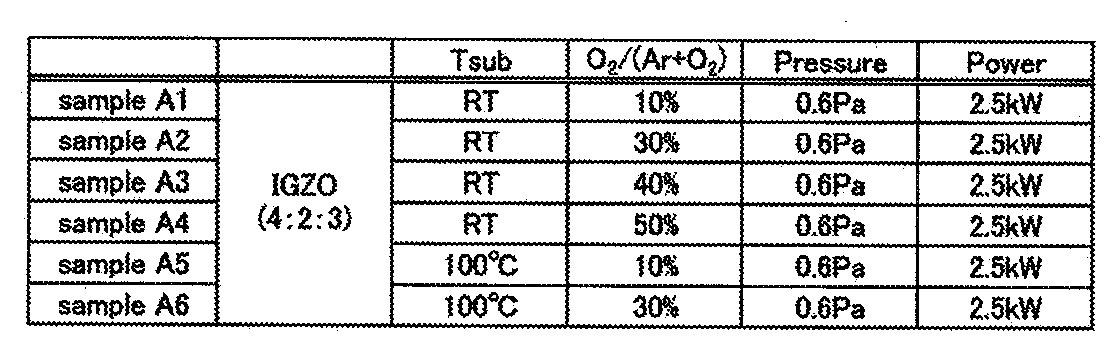
sample A1乃至sample A6をそれぞれ、金属酸化物膜の被形成面に平行な方向に薄片化し、厚さを約20nm乃至30nmとした。薄片化後の試料は、金属酸化物膜を成膜した際の金属酸化物膜の表面を含む。
次に、sample A1乃至sample A6のX線回折(XRD)分析を行った。
本項では、極微小な結晶領域を有する金属酸化物膜(以下、nc膜ともいう)の安定性について、第一原理計算の結果を用いて説明する。
以下では、計算モデル1Aの作成方法について説明する。
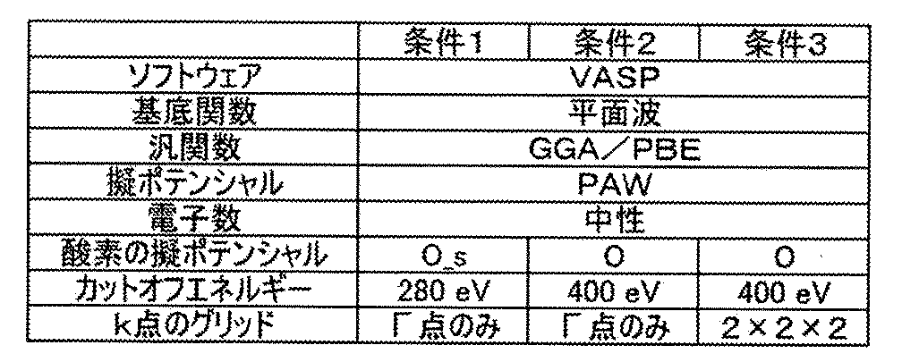
以下では、計算モデル2Aの作成方法について説明する。なお、計算モデル2Aを作成するための計算は、表2に示す計算条件を用いる。
本項では、nc膜の熱安定性について、第一原理計算の結果を用いて説明する。なお、nc膜の熱安定性は、後述する内部エネルギーを用いて評価する。

本項では、nc膜における欠陥の生成しやすさについて、第一原理計算の結果を用いて説明する。具体的には、酸素欠損に水素が入った欠陥(以下、VOHまたはHOと呼ぶ場合がある。)の生成エネルギーを、第一原理計算より算出する。

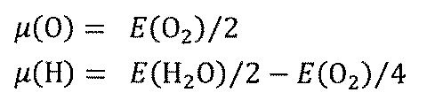
酸化物半導体(金属酸化物)は、単結晶酸化物半導体と、それ以外の非単結晶酸化物半導体と、に分けられる。非単結晶酸化物半導体としては、例えば、CAAC−OS(c−axis aligned crystalline oxide semiconductor)、多結晶酸化物半導体、nc−OS(nanocrystalline oxide semiconductor)、擬似非晶質酸化物半導体(a−like OS:amorphous−like oxide semiconductor)、および非晶質酸化物半導体などがある。
CAC−OSとは、材料の一部では導電性の機能と、材料の一部では絶縁性の機能とを有し、材料の全体では半導体としての機能を有する。なお、CAC−OSを、トランジスタの活性層に用いる場合、導電性の機能は、キャリアとなる電子(またはホール)を流す機能であり、絶縁性の機能は、キャリアとなる電子を流さない機能である。導電性の機能と、絶縁性の機能とを、それぞれ相補的に作用させることで、スイッチングさせる機能(On/Offさせる機能)をCAC−OSに付与することができる。CAC−OSにおいて、それぞれの機能を分離させることで、双方の機能を最大限に高めることができる。
本実施の形態では、本発明の一態様の金属酸化物膜を適用した半導体装置の構成例について説明する。以下では、トランジスタを例に挙げて説明する。
〔構成例1−1〕
図23Aは、トランジスタ300の上面図であり、図23Bは、図23Aに示す一点鎖線A1−A2における切断面の断面図に相当し、図23Cは、図23Aに示す一点鎖線B1−B2における切断面の断面図に相当する。一点鎖線A1−A2方向はチャネル長方向、一点鎖線B1−B2方向はチャネル幅方向に相当する。なお、図23Aにおいて、トランジスタ300の構成要素の一部(ゲート絶縁層等)を省略して図示している。また、トランジスタの上面図については、以降の図面においても図23Aと同様に、構成要素の一部を省略して図示する。
以下では、上記構成例1−1と一部の構成が異なるトランジスタの構成例について説明する。なお、以下では、上記構成例1−1と重複する部分は説明を省略する場合がある。
以下では、上記構成例1とは異なるトランジスタの構成例について説明する。
図25Aは、トランジスタ350の上面図であり、図25Bは、図25Aに示す一点鎖線A3−A4における切断面の断面図に相当し、図25Cは、図25Aに示す一点鎖線B3−B4における切断面の断面図に相当する。一点鎖線A3−A4方向はチャネル長方向、一点鎖線B3−B4方向はチャネル幅方向に相当する。
図26Aは、トランジスタ350Aの上面図であり、図26Bは、トランジスタ350Aのチャネル長方向の断面図であり、図26Cは、トランジスタ350Aのチャネル幅方向の断面図である。
図27Aに、トランジスタ350Bの断面図を示している。図27Aでは、一点鎖線よりも左側にチャネル長方向の断面を、右側にチャネル幅方向の断面を、並べて明示している。
図27Bに、トランジスタ350Cの断面図を示している。図27Bでは、一点鎖線よりも左側にチャネル長方向の断面を、右側にチャネル幅方向の断面を、並べて明示している。
本実施の形態では、本発明の一態様の金属酸化物膜を有する半導体装置を用いて作製できる表示装置の構成例について説明する。
以下では、表示装置の断面構成例について説明する。
図29に、表示装置700の断面概略図を示す。図29は、図28Aで示した表示装置700の表示部702と、回路部763と、湾曲部761aと、接続端子703aと、を含む断面を示している。表示部702には、トランジスタ750及び容量素子790が設けられている。回路部763には、トランジスタ752が設けられている。
図30には、図29とは一部の構成が異なる表示装置700の断面図を示している。また、図30では、湾曲部761aにおいて表示装置700の一部が湾曲し、表示面側とは反対側に折り返された形態を明示している。
図31には、表示素子として液晶素子を用いた場合の、表示装置700aの断面概略図を示している。図31では、回路部763、表示部702、及び接続端子703aを含む領域の断面図を示している。
本実施の形態では、本発明の一態様の半導体装置を有する表示装置について、図32A乃至図32Cを用いて説明を行う。
以下では、画素に表示される階調を補正するためのメモリを備える画素回路と、これを有する表示装置について説明する。実施の形態1で例示した金属酸化物膜を有するトランジスタは、以下で例示する画素回路に用いられるトランジスタに適用することができる。
図33Aに、画素回路400の回路図を示す。画素回路400は、トランジスタM1、トランジスタM2、容量C1、及び回路401を有する。また画素回路400には、配線S1、配線S2、配線G1、及び配線G2が接続される。
続いて、図33Bを用いて、画素回路400の動作方法の一例を説明する。図33Bは、画素回路400の動作に係るタイミングチャートである。なおここでは説明を容易にするため、配線抵抗などの各種抵抗や、トランジスタや配線などの寄生容量、及びトランジスタのしきい値電圧などの影響は考慮しない。
期間T1では、配線G1と配線G2の両方に、トランジスタをオン状態にする電位を与える。また、配線S1には定電位である電位Vrefを供給し、配線S2には第1データ電位Vwを供給する。
続いて期間T2では、配線G1にはトランジスタM1をオン状態とする電位を与え、配線G2にはトランジスタM2をオフ状態とする電位を与える。また、配線S1には第2データ電位Vdataを供給する。配線S2には所定の定電位を与える、またはフローティング状態としてもよい。
〔液晶素子を用いた例〕
図33Cに示す画素回路400LCは、回路401LCを有する。回路401LCは、液晶素子LCと、容量C2とを有する。
図33Dに示す画素回路400ELは、回路401ELを有する。回路401ELは、発光素子EL、トランジスタM3、及び容量C2を有する。
本実施の形態では、本発明の一態様を用いて作製することができる表示モジュールについて説明する。
本実施の形態では、本発明の一態様の表示装置を適用可能な、電子機器の例について説明する。
本実施の形態では、本発明の一態様を用いて作製された表示装置を備える電子機器について説明する。
作製したトランジスタの構成は、実施の形態2の構成例2−3及び図27Aで例示したトランジスタ350Bを援用できる。
続いて、上記で作製したトランジスタのId−Vg特性を測定した。
続いて、上記Sample B1乃至Sample B4について、信頼性の評価を行った。信頼性の評価として、ゲートバイアスストレス試験(GBT試験)を行った。GBT試験は、トランジスタが形成されている基板を60℃に保持し、トランジスタのソースとドレインに0V、ゲートには20Vまたは−20Vの電圧を印加し、この状態を一時間保持した。ここでは特に、PBTS試験及びNBTIS試験の結果について示す。なお、NBTISにおける光の照射は、約3400lxの白色LED光を用いた。また、ここで測定したトランジスタは、設計値がチャネル長2μm、チャネル幅3μmのトランジスタとした。
本実施例で用いた試料は、ガラス基板上にスパッタリング法により金属酸化物膜を成膜したものである。金属酸化物膜の成膜は、金属元素の原子数比がIn:Ga:Zn=4:2:4.1[原子数比]である金属酸化物ターゲットを用いた。成膜ガスとしては、アルゴンガスと酸素ガスの混合ガスを用いた。また、金属酸化物膜の成膜は、基板を加熱することなく行った。ここで、金属酸化物膜の成膜条件を異ならせた3つの試料(Sample C1乃至Sample C3)を作製した。
作製した3つの試料について、高角散乱環状暗視野走査透過電子顕微鏡法(HAADF−STEM:High−Angle Annular Dark Field Scanning Transmission Electron Microscopy)による観察と、エネルギー分散型X線分光法(EDX:Energy Dispersive X−ray Spectroscopy)による組成分析を行った。
続いて、各試料について、上記InのEDXマッピング像における明るい領域(In−rich領域)、及び、暗い領域(In−poor領域)、ならびにGaのEDXマッピング像における明るい領域(Ga−rich領域)、及び、暗い領域(Ga−poor領域)のそれぞれについて、In、Ga、及びZnについて定量分析を行った。定量分析は、各5ポイントについて行った。
続いて、図42に示す各EDXマッピング像全体について定量分析を行い、得られたIn、Ga、及びZnそれぞれの組成について、ヒストグラムを用いた解析を行った。
Claims (6)
- インジウム、M(Mはアルミニウム、ガリウム、イットリウム、またはスズ)、及び亜鉛を含む金属酸化物膜であって、
前記金属酸化物膜の膜面に垂直な方向から電子線を照射する電子線回折で決定される面間隔dの分布が、第1のピークと、第2のピークとを有し、
前記第1のピークの頂点が、0.25nm以上0.30nm以下に位置し、
前記第2のピークの頂点が、0.15nm以上0.20nm以下に位置し、
前記面間隔dの分布は、前記金属酸化物膜の複数の領域における複数の電子線回折パターンから得られるものであり、
前記電子線回折は、ビーム径が0.3nm以上10nm以下である電子線を用いて行われる、
金属酸化物膜。 - 請求項1において、
前記第1のピークの頂点の高さが、前記第2のピークの頂点の高さよりも高い、
金属酸化物膜。 - 請求項1において、
前記第1のピークの頂点の高さが、前記第2のピークの頂点の高さよりも低い、
金属酸化物膜。 - 半導体層と、ゲート電極と、ゲート絶縁層と、を有し、
前記半導体層は、請求項1乃至請求項3のいずれか一に記載の金属酸化物膜を含む、
半導体装置。 - 金属酸化物膜の複数の領域に対して、前記金属酸化物膜の膜面に垂直な方向から、ビーム径が0.3nm以上10nm以下である電子線を照射して、複数の電子線回折パターンを取得し、
複数の前記電子線回折パターンで観測される複数のスポットに対して、面間隔dを算出し、
前記面間隔dの度数分布の形状から、前記金属酸化物膜の結晶性を評価する、
金属酸化物膜の評価方法。 - 金属酸化物膜の複数の領域に対して、前記金属酸化物膜の膜面に垂直な方向から、ビーム径が0.3nm以上10nm以下である電子線を照射して、複数の電子線回折パターンを取得し、
複数の前記電子線回折パターンで観測される複数のスポットに対して、基準線からの角度θを算出し、
前記角度θの分布の形状から、前記金属酸化物膜の結晶性を評価する、
金属酸化物膜の評価方法。
Priority Applications (6)
| Application Number | Priority Date | Filing Date | Title |
|---|---|---|---|
| KR1020217028896A KR20210130172A (ko) | 2019-02-22 | 2020-02-10 | 금속 산화물막, 반도체 장치, 및 금속 산화물막의 평가 방법 |
| JP2021501126A JP7531478B2 (ja) | 2019-02-22 | 2020-02-10 | 金属酸化物膜の評価方法 |
| CN202080014352.6A CN113423857A (zh) | 2019-02-22 | 2020-02-10 | 金属氧化物膜、半导体装置及金属氧化物膜的评价方法 |
| US17/431,275 US20220127713A1 (en) | 2019-02-22 | 2020-02-10 | Metal oxide film, semiconductor device, and method for evaluating metal oxide film |
| US18/668,768 US20240321577A1 (en) | 2019-02-22 | 2024-05-20 | Metal oxide film, semiconductor device, and method for evaluating metal oxide film |
| JP2024123143A JP2024149553A (ja) | 2019-02-22 | 2024-07-30 | 金属酸化物膜 |
Applications Claiming Priority (6)
| Application Number | Priority Date | Filing Date | Title |
|---|---|---|---|
| JP2019030643 | 2019-02-22 | ||
| JP2019-030643 | 2019-02-22 | ||
| JP2019-042866 | 2019-03-08 | ||
| JP2019042866 | 2019-03-08 | ||
| JP2019076585 | 2019-04-12 | ||
| JP2019-076585 | 2019-04-12 |
Related Child Applications (2)
| Application Number | Title | Priority Date | Filing Date |
|---|---|---|---|
| US17/431,275 A-371-Of-International US20220127713A1 (en) | 2019-02-22 | 2020-02-10 | Metal oxide film, semiconductor device, and method for evaluating metal oxide film |
| US18/668,768 Division US20240321577A1 (en) | 2019-02-22 | 2024-05-20 | Metal oxide film, semiconductor device, and method for evaluating metal oxide film |
Publications (1)
| Publication Number | Publication Date |
|---|---|
| WO2020170065A1 true WO2020170065A1 (ja) | 2020-08-27 |
Family
ID=72144853
Family Applications (1)
| Application Number | Title | Priority Date | Filing Date |
|---|---|---|---|
| PCT/IB2020/050999 Ceased WO2020170065A1 (ja) | 2019-02-22 | 2020-02-10 | 金属酸化物膜、半導体装置、及び金属酸化物膜の評価方法 |
Country Status (6)
| Country | Link |
|---|---|
| US (2) | US20220127713A1 (ja) |
| JP (2) | JP7531478B2 (ja) |
| KR (1) | KR20210130172A (ja) |
| CN (1) | CN113423857A (ja) |
| TW (2) | TWI906872B (ja) |
| WO (1) | WO2020170065A1 (ja) |
Families Citing this family (4)
| Publication number | Priority date | Publication date | Assignee | Title |
|---|---|---|---|---|
| KR102255421B1 (ko) * | 2020-08-11 | 2021-05-24 | 충남대학교산학협력단 | 단결정 산화갈륨의 결함 평가방법 |
| KR20240051496A (ko) | 2022-10-13 | 2024-04-22 | 한국전기연구원 | 비파괴분석법을 이용한 와이드밴드갭 소재의 결함 평가방법 |
| US20250201633A1 (en) * | 2023-12-13 | 2025-06-19 | Taiwan Semiconductor Manufacturing Company, Ltd. | Thermal characterization method and manufacturing of semiconductor package |
| WO2025184557A1 (en) * | 2024-03-01 | 2025-09-04 | Gatan Inc. | Devices and systems for experimental forward model indexing of electron backscatter diffraction patterns |
Citations (2)
| Publication number | Priority date | Publication date | Assignee | Title |
|---|---|---|---|---|
| JP2017183718A (ja) * | 2016-03-25 | 2017-10-05 | 株式会社半導体エネルギー研究所 | トランジスタ、半導体装置、および電子機器 |
| JP2018006728A (ja) * | 2015-12-29 | 2018-01-11 | 株式会社半導体エネルギー研究所 | 金属酸化物膜、および半導体装置 |
Family Cites Families (5)
| Publication number | Priority date | Publication date | Assignee | Title |
|---|---|---|---|---|
| JP5451280B2 (ja) * | 2008-10-09 | 2014-03-26 | キヤノン株式会社 | ウルツ鉱型結晶成長用基板およびその製造方法ならびに半導体装置 |
| KR102071545B1 (ko) | 2012-05-31 | 2020-01-30 | 가부시키가이샤 한도오따이 에네루기 켄큐쇼 | 반도체 장치 |
| TWI643969B (zh) * | 2013-12-27 | 2018-12-11 | Semiconductor Energy Laboratory Co., Ltd. | 氧化物半導體的製造方法 |
| KR102526654B1 (ko) * | 2015-03-03 | 2023-04-26 | 가부시키가이샤 한도오따이 에네루기 켄큐쇼 | 산화물 반도체막, 상기 산화물 반도체막을 포함하는 반도체 장치, 및 상기 반도체 장치를 포함하는 표시 장치 |
| CN106409919A (zh) * | 2015-07-30 | 2017-02-15 | 株式会社半导体能源研究所 | 半导体装置以及包括该半导体装置的显示装置 |
-
2020
- 2020-02-10 US US17/431,275 patent/US20220127713A1/en not_active Abandoned
- 2020-02-10 CN CN202080014352.6A patent/CN113423857A/zh active Pending
- 2020-02-10 WO PCT/IB2020/050999 patent/WO2020170065A1/ja not_active Ceased
- 2020-02-10 TW TW113117698A patent/TWI906872B/zh active
- 2020-02-10 JP JP2021501126A patent/JP7531478B2/ja active Active
- 2020-02-10 TW TW109104004A patent/TWI844622B/zh active
- 2020-02-10 KR KR1020217028896A patent/KR20210130172A/ko not_active Ceased
-
2024
- 2024-05-20 US US18/668,768 patent/US20240321577A1/en active Pending
- 2024-07-30 JP JP2024123143A patent/JP2024149553A/ja not_active Withdrawn
Patent Citations (2)
| Publication number | Priority date | Publication date | Assignee | Title |
|---|---|---|---|---|
| JP2018006728A (ja) * | 2015-12-29 | 2018-01-11 | 株式会社半導体エネルギー研究所 | 金属酸化物膜、および半導体装置 |
| JP2017183718A (ja) * | 2016-03-25 | 2017-10-05 | 株式会社半導体エネルギー研究所 | トランジスタ、半導体装置、および電子機器 |
Also Published As
| Publication number | Publication date |
|---|---|
| TW202508972A (zh) | 2025-03-01 |
| TWI906872B (zh) | 2025-12-01 |
| KR20210130172A (ko) | 2021-10-29 |
| CN113423857A (zh) | 2021-09-21 |
| US20240321577A1 (en) | 2024-09-26 |
| JP2024149553A (ja) | 2024-10-18 |
| US20220127713A1 (en) | 2022-04-28 |
| TWI844622B (zh) | 2024-06-11 |
| JP7531478B2 (ja) | 2024-08-09 |
| TW202104086A (zh) | 2021-02-01 |
| JPWO2020170065A1 (ja) | 2020-08-27 |
Similar Documents
| Publication | Publication Date | Title |
|---|---|---|
| JP7682962B2 (ja) | 半導体装置の作製方法 | |
| JP7612791B2 (ja) | 半導体装置の作製方法 | |
| JP7077294B2 (ja) | 複合酸化物半導体、半導体装置及び表示装置 | |
| JP7813338B2 (ja) | 半導体装置 | |
| JP2022016470A (ja) | トランジスタ | |
| JP7531478B2 (ja) | 金属酸化物膜の評価方法 | |
| JP2025181971A (ja) | 半導体装置 | |
| JP2021166313A (ja) | トランジスタ | |
| WO2020089726A1 (ja) | 半導体装置 | |
| JP2025028909A (ja) | 半導体装置 | |
| JP7672968B2 (ja) | トランジスタ | |
| WO2019175708A1 (ja) | 半導体装置、および半導体装置の作製方法 | |
| JPWO2020074993A1 (ja) | 半導体装置 | |
| JPWO2020012276A1 (ja) | 半導体装置 | |
| WO2019186315A1 (ja) | 半導体装置、および半導体装置の作製方法 | |
| WO2022106943A1 (ja) | 半導体装置、表示装置、表示モジュール、及び電子機器 | |
| JP7275112B2 (ja) | 半導体装置 |
Legal Events
| Date | Code | Title | Description |
|---|---|---|---|
| 121 | Ep: the epo has been informed by wipo that ep was designated in this application |
Ref document number: 20759721 Country of ref document: EP Kind code of ref document: A1 |
|
| ENP | Entry into the national phase |
Ref document number: 2021501126 Country of ref document: JP Kind code of ref document: A |
|
| NENP | Non-entry into the national phase |
Ref country code: DE |
|
| ENP | Entry into the national phase |
Ref document number: 20217028896 Country of ref document: KR Kind code of ref document: A |
|
| 122 | Ep: pct application non-entry in european phase |
Ref document number: 20759721 Country of ref document: EP Kind code of ref document: A1 |
|
| WWR | Wipo information: refused in national office |
Ref document number: 1020217028896 Country of ref document: KR |