WO2020166645A1 - デジタル位相同期回路、デジタル制御発振器、デジタル-時間変換器 - Google Patents
デジタル位相同期回路、デジタル制御発振器、デジタル-時間変換器 Download PDFInfo
- Publication number
- WO2020166645A1 WO2020166645A1 PCT/JP2020/005456 JP2020005456W WO2020166645A1 WO 2020166645 A1 WO2020166645 A1 WO 2020166645A1 JP 2020005456 W JP2020005456 W JP 2020005456W WO 2020166645 A1 WO2020166645 A1 WO 2020166645A1
- Authority
- WO
- WIPO (PCT)
- Prior art keywords
- circuit
- frequency
- clock
- output
- reference clock
- Prior art date
- Legal status (The legal status is an assumption and is not a legal conclusion. Google has not performed a legal analysis and makes no representation as to the accuracy of the status listed.)
- Ceased
Links
Images











Classifications
-
- H—ELECTRICITY
- H03—ELECTRONIC CIRCUITRY
- H03L—AUTOMATIC CONTROL, STARTING, SYNCHRONISATION OR STABILISATION OF GENERATORS OF ELECTRONIC OSCILLATIONS OR PULSES
- H03L7/00—Automatic control of frequency or phase; Synchronisation
- H03L7/06—Automatic control of frequency or phase; Synchronisation using a reference signal applied to a frequency- or phase-locked loop
- H03L7/08—Details of the phase-locked loop
- H03L7/099—Details of the phase-locked loop concerning mainly the controlled oscillator of the loop
- H03L7/0991—Details of the phase-locked loop concerning mainly the controlled oscillator of the loop the oscillator being a digital oscillator, e.g. composed of a fixed oscillator followed by a variable frequency divider
-
- H—ELECTRICITY
- H03—ELECTRONIC CIRCUITRY
- H03K—PULSE TECHNIQUE
- H03K5/00—Manipulating of pulses not covered by one of the other main groups of this subclass
- H03K5/01—Shaping pulses
-
- G—PHYSICS
- G06—COMPUTING OR CALCULATING; COUNTING
- G06F—ELECTRIC DIGITAL DATA PROCESSING
- G06F1/00—Details not covered by groups G06F3/00 - G06F13/00 and G06F21/00
- G06F1/04—Generating or distributing clock signals or signals derived directly therefrom
- G06F1/06—Clock generators producing several clock signals
-
- G—PHYSICS
- G06—COMPUTING OR CALCULATING; COUNTING
- G06F—ELECTRIC DIGITAL DATA PROCESSING
- G06F1/00—Details not covered by groups G06F3/00 - G06F13/00 and G06F21/00
- G06F1/04—Generating or distributing clock signals or signals derived directly therefrom
- G06F1/08—Clock generators with changeable or programmable clock frequency
-
- H—ELECTRICITY
- H03—ELECTRONIC CIRCUITRY
- H03B—GENERATION OF OSCILLATIONS, DIRECTLY OR BY FREQUENCY-CHANGING, BY CIRCUITS EMPLOYING ACTIVE ELEMENTS WHICH OPERATE IN A NON-SWITCHING MANNER; GENERATION OF NOISE BY SUCH CIRCUITS
- H03B5/00—Generation of oscillations using amplifier with regenerative feedback from output to input
- H03B5/02—Details
-
- H—ELECTRICITY
- H03—ELECTRONIC CIRCUITRY
- H03K—PULSE TECHNIQUE
- H03K5/00—Manipulating of pulses not covered by one of the other main groups of this subclass
- H03K5/13—Arrangements having a single output and transforming input signals into pulses delivered at desired time intervals
-
- H—ELECTRICITY
- H03—ELECTRONIC CIRCUITRY
- H03M—CODING; DECODING; CODE CONVERSION IN GENERAL
- H03M1/00—Analogue/digital conversion; Digital/analogue conversion
- H03M1/66—Digital/analogue converters
- H03M1/82—Digital/analogue converters with intermediate conversion to time interval
-
- H—ELECTRICITY
- H03—ELECTRONIC CIRCUITRY
- H03K—PULSE TECHNIQUE
- H03K5/00—Manipulating of pulses not covered by one of the other main groups of this subclass
- H03K2005/00013—Delay, i.e. output pulse is delayed after input pulse and pulse length of output pulse is dependent on pulse length of input pulse
- H03K2005/00078—Fixed delay
-
- H—ELECTRICITY
- H03—ELECTRONIC CIRCUITRY
- H03L—AUTOMATIC CONTROL, STARTING, SYNCHRONISATION OR STABILISATION OF GENERATORS OF ELECTRONIC OSCILLATIONS OR PULSES
- H03L2207/00—Indexing scheme relating to automatic control of frequency or phase and to synchronisation
- H03L2207/50—All digital phase-locked loop
Definitions
- the present invention relates to a digital phase synchronization circuit, a digitally controlled oscillator, and a digital-time converter.
- a phase locked loop (Phase Locked Loop) is used to multiply the reference clock and generate a clock of any frequency.
- a digital PLL circuit (D-PLL: Digital PLL) is known as one form of the PLL circuit.
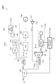
- FIG. 1 is a circuit diagram showing the basic architecture of a fractional frequency division type (Fractional-N) D-PLL circuit 100R.
- the D-PLL circuit 100R receives the reference clock REF and a frequency control word (FCW: Frequency Control Word) designating a multiplication number and generates an output clock OUT by multiplying the reference clock REF according to the FCW.
- FCW Frequency Control Word
- Digital-to-time converter (DTC) 102 time-to-digital converter (TDC) 104, digital loop filter (DLF: Digital Loop Filter) 106, digitally controlled oscillator ( A DCO (Digitally-Controlled Oscillator) 108, a buffer 110, a multi-modulous divider (MMD) 112, a controller 114, and a retiming circuit 116 are provided.
- DTC Digital-to-time converter
- TDC time-to-digital converter
- DDF Digital Loop Filter
- a DCO Digitally-Controlled Oscillator
- MMD multi-modulous divider
- the DCO108 oscillates at a frequency corresponding to the digital control data D CNT.
- the output clock OUT of the DCO 108 is input to the MMD 112 via the buffer 110.
- the MMD 112 divides the output clock OUT by the division ratio set by the controller 114.
- the controller 114 is designed based on the architecture of the ⁇ modulator. In the fractional-N type PLL circuit, the controller 114 switches the frequency division ratio of the MMD 112 in a time division manner with a plurality of integer values in order to obtain a multiplication ratio of fraction. The reciprocal of the average value of the frequency division ratios set in the MMD 112 becomes the multiplication ratio N F of the D-PLL circuit 100.
- the divided clock DIV is input to the retiming circuit 116.
- the retiming circuit 116 retimes the divided clock DIV by the output clock CKV that has passed through the buffer 110 to generate the feedback clock FB.
- the DTC 102 gives a delay set by the controller 114 to the reference clock REF and outputs the reference clock REFA. This delay amount is selected according to the frequency division ratio given to the MMD 112.
- the TDC 104 converts the time difference between the reference clock REFA and the feedback clock FB into a digital value.
- the DLF 106 removes the high frequency component of the output of the TDC 104 and generates the control data D CNT .
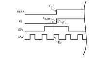
- FIG. 2 is a time chart of the D-PLL circuit 100R of FIG.
- the divided clock DIV is retimed by the clock CKV. Due to the sampling delay ⁇ SAM in the retiming circuit 116, the edge E 1 of the feedback clock FB is delayed by ⁇ SAM with respect to the edge E 2 of the clock CKV.
- the feedback loop including the TDC 104 and the DLF 106 performs feedback so that the time difference between the edge E 3 of the reference clock REFA and the edge E 1 of the feedback clock FB becomes zero, and the phase is locked.
- the frequency of the output clock OUT (and CKV) of the DCO 108 is N F times the frequency of the reference clock REFA (and REF).
- the D-PLL circuit 100R of FIG. 1 has the advantages of high frequency accuracy and robustness against frequency interference. However, since the MMD 112 and the retiming circuit 116 continue to operate in synchronization with the high frequency clock CKV, there is a problem that the power consumption is large.
- the present invention has been made in view of the above problems, and one of exemplary purposes of a certain aspect thereof is to provide a D-PLL circuit with reduced power consumption.
- An aspect of the present invention relates to a phase locked loop circuit that receives a first reference clock and generates an output clock.
- the phase synchronization circuit delays the first reference clock to generate a second reference clock, a second reference clock, a feedback circuit that generates a control signal according to a phase difference between the feedback clock, and a control signal.
- An oscillator that oscillates at an appropriate frequency and generates an output clock, and a frequency divider that can be switched on and off and that divides the output clock in the on state are provided.
- the phase locked loop circuit can switch between the first mode and the second mode. In the first mode, the feedback clock is a signal obtained by retiming the output of the frequency divider with the output clock. In the second mode, the feedback clock is a signal obtained by retiming the first reference clock with the output clock.
- One aspect of the present invention relates to a digital phase synchronization circuit that receives an input reference clock and a frequency control word and generates an output clock.
- the digital phase-locked loop circuit receives an input reference clock, a digital-time converter for generating a first reference clock, a delay circuit for delaying the first reference clock and a second reference clock, and a second reference clock.
- Time-digital converter that converts the phase difference of the feedback clock into a digital signal
- a digital control oscillator that oscillates at the frequency according to the output of the time-digital converter to generate the output clock, and can be switched on and off
- a frequency divider that divides the output clock by a frequency division ratio according to the frequency control word in the ON state.
- the feedback clock is a signal obtained by retiming the output of the frequency divider with the output clock.
- the feedback clock is the first reference signal. This is a signal obtained by retiming the clock with the output clock.
- This digitally controlled oscillator includes an upper unit and a lower unit that are vertically stacked between a power supply line and a ground line, and a variable capacitor that is connected to at least one of the upper unit and the lower unit.
- the upper unit and the lower unit each include a pair of cross-coupled circuit elements and an inductor connected to the pair of circuit elements.
- the transformers are formed by connecting the inductors of the upper unit and the lower unit.
- the digital-time converter is a digital-time converter that receives an input signal, delays it according to a control code, and generates an output signal.
- the digital-time converter includes a capacitor and a current source and generates a slope voltage.
- a control circuit for controlling the slope generation circuit and the precharge circuit.
- the control circuit turns on the precharge circuit in (i) the precharge period, transitions to the slope period in response to the input signal (ii), turns off the precharge circuit and turns on the slope generation circuit in the slope period, iii) The operation of turning off the slope generation circuit is repeated in response to the transition of the output signal.
- FIG. 3 is a circuit diagram showing a basic architecture of a fractional frequency division type (Fractional-N) D-PLL circuit.
- 3 is a time chart of the D-PLL circuit of FIG.
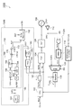
- FIG. 3 is a circuit diagram showing a basic architecture of the D-PLL circuit according to the exemplary embodiment.
- FIGS. 6A and 6B are time charts showing the operations of the D-PLL circuit in the sampling mode and the subsampling mode in comparison. It is a waveform diagram of the output frequency f OUT of the D-PLL circuit in the sub-sampling mode.
- FIG. 3 is a circuit diagram of a D-PLL circuit according to the first embodiment.
- FIG. 9A and 9B are diagrams for explaining the operation of the mode selector in the D-PLL circuit of FIG.
- FIG. 6 is a circuit diagram of a D-PLL circuit according to a second embodiment. It is a figure explaining operation
- FIG. 9 is a waveform diagram of an output frequency f OUT of the D-PLL circuit of FIG. 8.
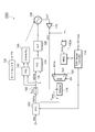
- FIG. 6 is a circuit diagram of a D-PLL circuit according to a third embodiment.
- 14A and 14B are circuit diagrams of a conventional DCO. It is a circuit diagram which shows the basic architecture of DCO which concerns on embodiment.
- FIG. 9A and 9B are diagrams for explaining the operation of the mode selector in the D-PLL circuit of FIG.
- FIG. 6 is a circuit diagram of a D-PLL circuit according to a second embodiment. It is a
- FIG. 16 is an equivalent circuit diagram of the DCO of FIG. 15. It is a figure which shows the relationship between the bias current I BIAS and the amplitude V AMP of an output signal.
- 9 is a circuit diagram of a DCO according to Modification 1.
- FIG. 9 is a circuit diagram of a DCO according to Modification 2.
- 20A to 20F are circuit diagrams showing further modifications of the DCO.
- It is a circuit diagram of the conventional DTC.
- FIG. 22 is an operation waveform diagram of the DTC in FIG. 21.
- It is a circuit diagram of DTC according to the embodiment.
- 24 is a time chart explaining the operation of the DTC of FIG. 23. It is a figure which shows the operation waveform (i) of DTC which concerns on this Embodiment, and the operation waveform (ii) of the conventional DTC.
- phase locked loop circuit that receives a first reference clock and generates an output clock.
- the phase synchronization circuit delays the first reference clock to generate a second reference clock, a second reference clock, a feedback circuit that generates a control signal according to a phase difference between the feedback clock, and a control signal.
- An oscillator that oscillates at an appropriate frequency and generates an output clock, and a frequency divider that can be switched on and off and that divides the output clock in the on state are provided.
- the phase locked loop circuit can switch between the first mode and the second mode.
- the feedback clock In the first mode, the feedback clock is a signal obtained by retiming the output of the frequency divider with the output clock.
- the feedback clock is a signal obtained by retiming the first reference clock with the output clock.
- the power consumption can be reduced by stopping the operation of the frequency divider by selecting the second mode and applying the phase synchronization with the second reference clock as the feedback clock.
- the first mode it is possible to return to the phase locked state when the phase locked is lost.
- the phase locked loop circuit receives a mode controller that generates an enable signal indicating the first mode and the second mode, an output of the frequency divider, and a first reference clock, and selects one of them according to the enable signal. And a retiming circuit for retiming the output of the multiplexer with an output clock. ON/OFF of the frequency divider may be controlled according to the enable signal, and the output of the retiming circuit may be a feedback clock.
- the phase locked loop circuit further includes a dead zone detector that determines whether a phase error between the second reference clock and the feedback clock is within a dead zone range.
- the output of the dead zone detector may be used. As a result, it is possible to prevent the mode from falling into a mode in which phase synchronization is not applied.
- the dead zone detector compares the phase difference or frequency difference between the second reference clock and the feedback clock and outputs a pulse based on the comparison result, and based on the output of the phase frequency detector.
- a determination unit that generates a phase error and determines whether or not the phase error is included in the dead zone may be included.
- the digital phase synchronization circuit monitors the relationship between the frequency of the output clock and the frequency of the input reference clock, and the frequency of the output clock deviates from the target frequency determined based on the frequency division ratio of the frequency divider.
- a frequency locked loop for detecting a frequency error may be further provided.
- the first mode and the second mode may correspond to the output of the frequency lock loop. This can prevent the phase lock from being applied at an incorrect frequency.
- the frequency lock loop may include a counter that counts the output clock for a period of K times (K is an integer) the cycle of the input reference clock.
- the frequency error may be detected based on the count value of the counter and a value obtained by multiplying the multiplication ratio, which is the reciprocal of the frequency division ratio, by K times.
- the phase locked loop circuit may further include a duty cycle controller that generates a control pulse having a predetermined duty ratio.
- the frequency lock loop may operate intermittently in response to the control pulse. By intermittently operating the frequency lock loop, an increase in power consumption can be suppressed.
- the digital phase synchronization circuit compares the phase difference or frequency difference between the second reference clock and the feedback clock, outputs a pulse based on the comparison result, and a phase frequency detector that is in operation in the first mode.
- a PLL (Phase Locked Loop) circuit that feedback-controls the frequency of the digitally controlled oscillator based on the output of the phase frequency detector may be further provided.
- the accuracy of the feedback loop including the phase frequency detector and the PLL circuit may be coarser than the accuracy of the feedback circuit. This makes it possible to quickly pull the lock state from the state in which the phase lock is released.
- the phase synchronization circuit may be a digital phase synchronization circuit.
- the feedback circuit may include a second reference clock and a time-to-digital converter that converts a phase difference of the feedback clock into a digital signal.
- the oscillator may be a digitally controlled oscillator that oscillates at a frequency according to the output of the time-to-digital converter.
- the phase synchronization circuit may be a fractional frequency division type.
- the frequency divider may be a multi-modulus frequency divider.
- the phase locked loop circuit includes a digital-to-time converter that receives an input reference clock and generates a first reference clock, and a digital-to-time converter and a multi-modulus frequency divider according to a frequency control word that specifies the frequency of the output clock. And a controller for controlling the.
- This digitally controlled oscillator includes an upper unit and a lower unit that are vertically stacked between a power supply line and a ground line, and a variable capacitor that is connected to at least one of the upper unit and the lower unit.
- the upper unit and the lower unit each include a pair of cross-coupled circuit elements and an inductor connected to the pair of circuit elements.
- the transformers are formed by connecting the inductors of the upper unit and the lower unit.
- the effect of gain amplification by the transformer can reduce the bias current for obtaining the same amplitude, or the amplitude can be increased when the bias current is maintained.
- At least one of the upper unit and the lower unit may be an N type in which a pair of circuit elements is an NMOS (N-channel Metal Oxide Semiconductor) transistor. Both the upper unit and the lower unit may be N-type.
- NMOS N-channel Metal Oxide Semiconductor
- At least one of the upper unit and the lower unit may be a P type in which a pair of circuit elements is a PMOS (P-channel Metal Oxide Semiconductor) transistor.
- PMOS P-channel Metal Oxide Semiconductor
- At least one of the upper unit and the lower unit may be a CMOS type in which a pair of circuit elements is a CMOS (Complementary Metal Oxide Semiconductor) inverter.
- CMOS Complementary Metal Oxide Semiconductor
- the digitally controlled oscillator may further include a bias current source inserted between the power supply line and the ground line.
- the digitally controlled oscillator may further include a capacitor connected to a connection node of the upper unit and the lower unit.
- the digital-to-time converter receives an input signal, delays it according to a control code, and generates an output signal.
- the digital-to-time converter includes a capacitor and a current source, a slope generation circuit that generates a slope voltage, a precharge circuit that applies an analog voltage according to the control code to the capacitor, and a slope voltage comparison with a threshold value. Then, it comprises a comparison means for generating an output signal according to the comparison result, and a control circuit for controlling the slope generation circuit and the precharge circuit according to the input signal and the output signal.
- the control circuit turns on the precharge circuit in (i) the precharge period, transitions to the slope period in response to the input signal (ii), turns off the precharge circuit and turns on the slope generation circuit in the slope period, iii) The operation of turning off the slope generation circuit is repeated in response to the transition of the output signal.
- the comparison means is configured to be switchable between on and off, and the control circuit may turn off the comparison means during the precharge period.
- the state in which the member A is connected to the member B means that the members A and B are electrically connected to each other in addition to the case where the members A and B are physically directly connected. It also includes the case of being indirectly connected through other members that do not substantially affect the general connection state or do not impair the functions and effects exerted by their connection.
- the state in which the member C is provided between the member A and the member B means that the members A and C or the members B and C are directly connected to each other, It also includes the case of being indirectly connected through other members that do not substantially affect the general connection state or do not impair the functions and effects exerted by their connection.
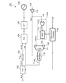
- FIG. 3 is a circuit diagram showing the basic architecture of the D-PLL circuit 100 according to the embodiment.
- the D-PLL circuit 100 is a fractional frequency division type PLL circuit, receives an input reference clock REF and a frequency control word FCW, and generates an output clock OUT having a frequency that is a fraction multiple of the frequency F of the input reference clock REF. ..
- the D-PLL circuit 100 further includes a multiplexer 120, a delay circuit 122, and a mode selector 130 in addition to the D-PLL circuit 100R of FIG. Further, the MMD 112A is configured to be switchable between enable/disable (on/off).
- the D-PLL circuit 100 can switch between two modes (referred to as a sampling mode and a subsampling mode), and the two modes are selected according to the enable signal EN.
- the enable signal EN is 1 (high)
- the D-PLL circuit 100 is set to the sampling mode
- the enable signal EN is 0 (low)
- the sub-sampling mode is set.
- the multiplexer 120 receives the divided clock DIV output from the MMD 112 and the first reference clock REFA output from the DTC 102, and selects one according to the enable signal EN.
- the output of the multiplexer 120 is retimed by the retiming circuit 116 and becomes the feedback clock FB.
- the output clock CKV passed through the buffer 110 can be used for retiming.
- the buffer 110 may be omitted if the output impedance of the DCO 108 is sufficiently low.
- the feedback clock FB is generated based on the divided clock DIV, and when it is 0 (low), the feedback clock FB is generated based on the first reference clock REFA.
- the function of the MMD 112A is the same as that of FIG. 1, but it is configured so that it can be turned on and off according to the enable signal EN.
- the MMD 112A includes a gate circuit 113 in addition to the MMD 112 of FIG.
- the gate circuit 113 is inserted in the preceding stage of the MMD 112, and gates the clock signal CKV according to the enable signal EN. That is, when the enable signal EN is 1, the clock CKG that has passed through the gate circuit 113 is input to the MMD 112, and the MMD 112 is enabled. When the EN signal is 0, the clock CKG is fixed low and thus the MMD 112 is disabled.
- the delay circuit 122 is inserted in the subsequent stage of the DTC 102, applies a delay ⁇ FB to the first reference clock REFA, and outputs the second reference clock REFB.
- the TDC 104 performs feedback so that the edge of the second reference clock REFB and the edge of the feedback clock FB match.
- the mode selector 130 generates an enable signal EN based on the operating state of the D-PLL circuit 100, and controls the mode of the D-PLL circuit 100.
- the operation of the MMD 112 is stopped. Since the frequency of the first reference clock REFA and the frequency of the divided clock DIV are equal, the first reference clock REFA is input to the retiming circuit 116 instead of the divided clock DIV. Then, the retiming circuit 116 retimes the first reference clock REFA at the edge of the clock signal CKV to generate the feedback clock FB.
- FIG. 5 is a time chart of the D-PLL circuit 100 in the sub sampling mode.
- the first reference clock REFA instead of the divided clock DIV, is retimed by the clock CKV. Due to the sampling delay ⁇ SAM in the retiming circuit 116, the edge E 1 of the feedback clock FB is delayed by ⁇ SAM with respect to the edge E 2 of the clock CKV.
- the feedback loop including the TDC 104 and the DLF 106 performs feedback so that the time difference between the edge E 4 of the second reference clock REFB and the edge E 1 of the feedback clock FB becomes zero, and the phase is locked.
- FB ) and the phase of the feedback clock FB delayed by retiming are included within one cycle of the clock signal CKV, and thus phase synchronization can be applied.
- FIGS. 6A and 6B are time charts showing the operations of the D-PLL circuit 100 in the sampling mode and the subsampling mode in comparison.
- the operation in the sampling mode of FIG. 6A is similar to that of FIG.
- the difference is that the phase of the feedback clock FB is locked on the basis of the phase of the second reference clock REFB instead of the first reference clock REFA.
- the operation of the sub-sampling mode of FIG. 6B is the same as that of FIG.
- the above is the operation of the D-PLL circuit 100. Then, the advantage is demonstrated.
- the D-PLL circuit 100 is operated in the sub-sampling mode, the operation of the MMD 112 is stopped, so that the power consumption can be significantly reduced compared to the sampling mode.
- the above is the basic architecture of the D-PLL circuit 100 according to the embodiment. Next, a specific implementation of the D-PLL circuit 100 will be described with reference to some embodiments.
- FIG. 7 is a waveform diagram (simulation) of the output frequency f OUT of the D-PLL circuit 100 in the sub sampling mode.
- FIG. 7 shows waveforms (i) to (iii) when the frequency interference of ⁇ 1 MHz, +6 MHz, and +11 MHz is injected. As shown in (i), when the frequency interference of -1 MHz is introduced, the phase locked state can be maintained.
- the mode selector 130 is mounted so as to monitor the state of the D-PLL circuit 100 and control the mode of the D-PLL circuit 100 so as not to fall into the situations (ii) and (iii) of FIG. 7. There is a need to.
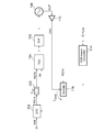
- FIG. 8 is a circuit diagram of the D-PLL circuit 100A according to the first embodiment.
- the mode selector 130A is configured to be able to detect a state in which the phases are not synchronized, as shown by the waveform (iii) in FIG.
- the mode selector 130A includes a dead zone detector 140 and a state machine 132.
- the dead zone detector 140 determines whether or not the phase error t ERR between REFB and FB is included in the range of the dead zone t DZ.
- the first level for example, high, 1
- a detection signal ODZ Out of Dead Zone which becomes the second level (for example, low, 0) is generated.
- the configuration of the dead zone detector 140 is not particularly limited, but includes, for example, a phase frequency detector (PFD: Phase Frequency Detector) 142 and a determination unit 144.
- the PFD 142 compares the phase difference or frequency difference between the second reference clock REFB and the feedback clock FB and outputs two pulses (UP pulse, DN pulse) based on the comparison result.
- the determination unit 144 receives the output UP/DN of the PFD 142 and generates the phase error t ERR based on them. Then, it is determined whether the phase error t ERR is included in the dead zone, and the ODZ signal is output.
- the state machine 132 synchronizes the ODZ signal with the reference clock REF to generate the enable signal EN.
- the state machine 132 can be composed of flip-flops.
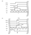
- FIG. 9A shows the input/output characteristics of the dead zone detector 140.
- FIG. 9B shows the operation of the entire D-PLL circuit 100A.
- the sub-sampling mode is in operation.
- the phase error t ERR between the feedback clock FB and the reference clock REFB deviates from the range of the dead zone t DZ for some reason, the ODZ signal periodically becomes high and the enable signal EN becomes high (1).
- the mode is switched to the sampling mode.
- the phase error t ERR becomes smaller, and when it returns to within the dead zone t DZ at time t 2 , the ODZ signal returns low.
- the enable signal EN goes low, and the subsampling mode is entered.
- FIG. 10 is a circuit diagram of the D-PLL circuit 100B according to the second embodiment.
- the mode selector 130B is configured to be able to detect frequency jumps of integral multiples as shown by the waveform (ii) in FIG.
- the mode selector 130B includes an intermittent operation frequency locked loop (FLL) 150 in addition to the dead zone detector 140 and the state machine 132.
- the intermittent operation FLL is also referred to as DC-FLL (Duty Cycled FLL).
- the intermittent operation FLL 150 includes a FLL 152 and a duty cycle controller 154.
- the FLL 152 is configured to be switchable between enable and disable. In the enabled state, the FLL 152 monitors the relationship between the frequency of the clock signal CKV(OUT) and the frequency of the reference clock REF, and when the frequency of the clock signal CKV deviates from the target frequency determined based on FCW, the frequency lock error signal. Assert FLE (eg, high). In other words, the FLL 152 monitors how many times the cycle of the reference clock REF is the cycle of the clock signal CKV, and determines whether or not it matches the multiplication ratio based on FCW. The state machine 132 switches the enable signal EN to high in response to the assertion of the frequency lock error signal FLE.
- Assert FLE eg, high
- the configuration of the FLL 152 is not limited, but includes, for example, a frequency detector 160, a subtractor 170, and a comparator 172.
- the frequency detector 160 includes a frequency divider 162, D flip-flops 164, 168, and a counter 166.
- the frequency-divided clock is synchronized with the clock CKV in the flip-flop 164.
- the counter 166 counts the number of pulses of the clock CKV.
- the flip-flop 168 fetches the count value of the counter 166 at the timing of the output of the frequency divider 162.
- the output of the flip-flop 168 indicates how many clocks CKV are included in the period K times the cycle of the reference clock REF.
- the subtractor 170 calculates the difference (frequency error) between the output of the flip-flop 168 and its target value (K ⁇ FCW).
- the comparator 172 compares the output of the subtractor 170 with a threshold value and asserts the frequency lock error signal FLE when the frequency error exceeds the allowable value.
- the duty ratio can be 1% or less, for example, about 0.5%. As a result, the power consumption of the FLL 152 can be reduced.
- FIG. 11 is a diagram for explaining the operation of the mode selector 130B in the D-PLL circuit 100B.
- the intermittent operation FLL 150 repeats turning on and off at a predetermined cycle. Then, when a frequency error is detected during the ON period, the mode shifts to the sampling mode and the frequency lock is performed.
- FIG. 11 shows the power consumption of the D-PLL circuit 100B.
- the power consumption during the suspension period of the intermittent operation FLL 150 is 262 ⁇ W, for example.
- the power consumption of the D-PLL circuit 100B jumps up (eg, 762 ⁇ W), but when the duty ratio is 0.5%, the average power consumption P AVE is 265 ⁇ W, which is only 3 ⁇ W. Can be suppressed to increase.
- the mode selector 130B can detect a frequency jump of an integral multiple, and in that case, by operating in the sampling mode, it is possible to prevent the phase synchronization from continuing in an erroneous state as shown in FIG. Since the mode selector 130B of FIG. 10 includes the dead zone detector 140 in addition to the intermittent operation FLL 150, it is possible to prevent the state of FIG. 7(iii) from occurring, as in the first embodiment.
- FIG. 12 is a waveform diagram (simulation) of the output frequency f OUT of the D-PLL circuit 100B of FIG. Similar to FIG. 7, waveforms (i) to (iii) when the frequency interference of ⁇ 1 MHz, +6 MHz, and +11 MHz is injected are shown. As shown in (i), when the frequency interference of -1 MHz is introduced, the phase locked state can be maintained.
- the dead zone detector 140 detects an abnormal state and switches to the sampling mode to restore the correct phase synchronization state.
- FIG. 13 is a circuit diagram of the D-PLL circuit 100C according to the third embodiment.
- a second coarse PLL circuit 180 is added to the D-PLL circuit 100C.
- the clock CKG is supplied to the second PLL circuit 180 when the enable signal EN is high.
- the second PLL circuit 180 is in an operating state during the period when the enable signal EN is high, that is, in the sub-sampling mode, and feedback-controls the frequency of the DCO 108 based on the output (UP/DN) of the PFD 182. That is, in the D-PLL circuit 100C of FIG.
- a highly accurate (Fine) feedback loop including the TDC 104 and the DLF 106 and a coarse (Coarse) feedback loop including the PFD 182 and the second PLL 180 operate in parallel.
- the PFD 182 can use the PFD 142 incorporated in the mode selector 130.
- the configuration of the mode selector 130 is not limited, and the first and second embodiments or other configurations can be adopted.
- the phase pull-in speed can be increased in the sub-sampling mode.
- Modification 1 A circuit in which the dead zone detector 140 is omitted from the mode selector 130B of FIG. 10 is also effective as an embodiment. In this case, an error that cannot be phase-synchronized may be dealt with by another method.
- Fractional-N PLL fractional frequency division type
- the present invention is not limited to this, and the present invention is also applicable to an integer frequency division type (Integer-N).
- the DTC 102 and the controller 114 may be deleted and the MMD 112 may be replaced with a simple frequency divider (Divider).
- the present invention can be applied not only to the D-PLL circuit but also to the analog PLL circuit.
- the set of TDC 104, DLF 106, and DCO 108 may be replaced with a phase frequency comparator (PFD), a charge pump circuit, an analog loop filter, and a voltage controlled oscillator (VCO).
- PFD phase frequency comparator
- VCO voltage controlled oscillator
- the DCO is an important elemental technology in the D-PLL circuit 100 or in other applications.
- 14A and 14B are circuit diagrams of a conventional DCO 200R.
- the DCO 200R is a CMOS oscillator and supplies a bias current to a pair of inverters 202 and 204 whose inputs and outputs are cross-coupled, a tank circuit 206 provided between the outputs of the pair of inverters 202 and 204, and a pair of inverters 202 and 204.
- a current source 208 for supply is provided.
- the tank circuit 206 is a parallel resonance circuit including an inductor L and a variable capacitor C.
- the resistance Rs is a series resistance component of the inductor L.
- the capacitance value of the variable capacitor Cs is digitally controllable, and the DCO 200R oscillates at an oscillation frequency according to the impedance of the tank circuit 206.
- FIG. 2 An equivalent circuit of the tank circuit 206 is shown in FIG.
- V AMP of the output of the DCO 200R in FIG. 14A is represented by the equation (1), and is proportional to the equivalent parallel resistance R TANK and the bias current I BIAS .
- the resistance R TANK is about 200 to 1000 ⁇ at most.
- the power consumption of the DCO 200R of FIG. 14(a) is limited by the impedance of the tank circuit.
- a novel DCO capable of further reducing power consumption will be described.
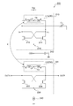
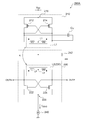
- FIG. 15 is a circuit diagram showing the basic architecture of the DCO 200 according to the embodiment.
- the DCO 200 includes an upper unit 210 and a lower unit 220.
- the upper unit 210 includes a pair of circuit elements 212 and 214, which are cross-coupled, and an inductor (primary winding) L1 provided with a tap T1.
- the inductor L1 is connected between the outputs (between the inputs) of the circuit element pair 212, 214.
- the tap T1 of the inductor L1 is directly connected to the power supply V DD , or a bias current source is connected as described later.
- the circuit elements 212 and 214 are NMOS transistors, and the sources of the NMOS transistors are connected to the reference node 216.
- the lower unit 220 includes a pair 222, 224 of cross-coupled circuit elements and an inductor L2 (secondary winding) provided with a tap T2.
- the inductor L2 is connected between the outputs (between the inputs) of the circuit element pair 212, 214.
- the tap T2 of the lower unit 220 is connected to the reference node 216 of the upper unit 210.
- the reference node 216 is connected to the capacitor 242 and serves as a virtual ground. This node is referred to as CEN.
- the circuit elements 222 and 224 are also NMOS transistors, and the sources of the NMOS transistors are commonly connected.
- the sources of the NMOS transistors 222 and 224 are connected to the reference node 226.
- a bias current source 240 is connected to the reference node 216.
- the one in which the cross-coupled circuit elements are NMOS transistors, like the upper unit 210 and the lower unit 220 in FIG. 15, is called an N-type unit.
- the inductor L1 of the upper unit 210 and the inductor L2 of the lower unit 220 are combined to form a transformer 230.
- the coupling coefficient between the winding Ls of the inductor L1 and the winding Lp of the inductor L2 is k.
- variable capacitor Cv is connected to the upper unit 210.
- the variable capacitor Cv forms an LC tank circuit together with the transformer 230, and the DCO 200 oscillates at a frequency according to the capacitance value of the variable capacitor Cv.
- the output extraction location is not particularly limited, but may be extracted from the drains of the NMOS transistors 222 and 224 of the lower unit 220, for example.
- V AMP of the output signal OUTP is represented by Expression (2).
- G TF is a gain by the transformer 230 and is represented by the equation (3).
- G TF k 2 ⁇ Ls/Lp+k ⁇ (Ls/Lp)+R TANKS /R TANKP (3)
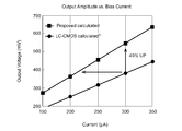
- FIG. 17 is a diagram (simulation) showing the relationship between the bias current I BIAS and the amplitude V AMP of the output signal.
- (I) shows the characteristics of the DCO 200 of FIG. 15, and (ii) shows the characteristics of the conventional DCO 200R. Comparing with the same bias current, according to the DCO 200 of FIG. 15, the amplitude can be increased by 46% as compared with the conventional one. In other words, the bias current required to obtain the same amplitude can be greatly reduced.
- FIG. 18 is a circuit diagram of the DCO 200A according to the first modification.
- the lower unit 220 is N-type like the lower unit 220 of FIG. 15, but the upper unit 210 is replaced with a P-type unit.
- the P-type unit has a configuration in which the pair of circuit elements 212 and 214 in the N-type unit are replaced with PMOS transistors and the top and bottom are inverted. Specifically, the inductor L1 is connected between the drains of the PMOS transistors 212 and 214, and the tap of the inductor L1 is connected to the virtual ground line CEN. The sources of the PMOS transistors 212 and 214 serve as the reference node 216, and the power supply voltage V DD is supplied.
- FIG. 19 is a circuit diagram of the DCO 200B according to the second modification.
- the upper unit 210 and the lower unit 220 are CMOS type (push-pull type) units.
- the pair of cross-coupled circuit elements is a CMOS inverter. Further, the tap of the inductor L can be omitted.
- 20A to 20F are circuit diagrams showing further modified examples of the DCO 200.
- N represents an N-type unit
- P represents a P-type unit
- C represents a CMOS-type unit.
- the combination of the upper unit 210 and the lower unit 220 is not limited to those described above.
- the upper unit 210 is a CMOS type and the lower unit 220 is an NMOS type.
- both the upper unit 210 and the lower unit 220 are PMOS type.
- the upper unit 210 is an NMOS type and the lower unit 220 is a CMOS type.
- the upper unit 210 is a PMOS type and the lower unit 220 is a CMOS type.
- the bias current source 240 may be omitted as shown in FIG. 20(e), or may be provided on the power supply side as shown in FIG. 20(f).
- the output signal of the DCO 200 may be taken out from the upper unit 210 side or the lower unit 220 side. Further, the variable capacitor Cv may be connected to the lower unit 220 side.
- TDC digital-to-time converter
- DTC digital-to-time converter
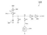
- FIG. 21 is a circuit diagram of a conventional DTC300R.
- This DTC300R is referred to as a single slope DTC.
- the DTC 300R includes a charging circuit 302, a capacitor 304, switches S1 to S3, inverters 306 and 308, and a DAC (D/A converter) 309.
- the DTC 300R delays the input signal IN according to the digital control code CODE and outputs it.
- the DAC 309 outputs the analog voltage V DAC according to the control code CODE.
- the charging circuit 302 charges the capacitor 304 when the first switch S1 is on.
- FIG. 22 is an operation waveform diagram of the DTC 300R of FIG.
- the third switch S3 is turned on, the capacitor 304 is discharged, and the voltage V P is initialized.
- the first switch S1 is turned on.
- the capacitor 304 is charged by the current I C of the charging circuit 302, and the voltage V P increases linearly.
- the DTC300R has room for reducing power consumption.
- the DTC with reduced power consumption will be described below.
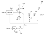
- FIG. 23 is a circuit diagram of the DTC 300 according to the embodiment.
- the DTC 300 includes a slope generation circuit 310, a precharge circuit 320, a comparison means 330, and a control circuit 340.
- the slope generation circuit 310 includes a capacitor 312, a current source 314 and a first switch S1.
- the current source 314 supplies a constant current Ic to the capacitor 312, and causes the capacitor 312 to generate a slope voltage V P that changes with a constant slope.
- the first switch S1 is provided to cut off the constant current Ic.
- the first switch S1 may be incorporated inside the current source 314.
- the precharge circuit 320 applies the analog voltage V DAC according to the control code CODE to the capacitor 312.
- the precharge circuit 320 includes a D/A converter 322 and a second switch S2. When the second switch S2 is on, the output voltage V DAC of the D/A converter 322 is applied to the capacitor 312, and when the second switch S2 is off, the capacitor 312 is disconnected from the capacitor 312. When the output of the D/A converter 322 can be in a high impedance state, the second switch S2 is omitted and the D/A converter 322 is controlled to realize the off state of the second switch S2. Good.
- the comparison means 330 compares the slope voltage V P generated in the capacitor 312 with the threshold value V TH, and generates the output signal OUT according to the comparison result.
- the comparison means 330 may include two stages of inverters 332 and 334 connected in a cascade.
- the slope voltage V P is compared with the threshold value of the inverter 332 by the first-stage inverter 332, and is converted into a binary signal according to the comparison result.
- the subsequent inverter 332 is provided to convert the logic value of the signal and/or provide a low impedance sufficient to drive the load.
- the comparison means 330 is configured to be switchable between on and off, and for that purpose, a third switch S3 is provided.
- the third switch S3 is provided between the inverter 332 and the ground.
- the third switch S3 may be inserted on the power supply line side.
- the control circuit 340 controls the slope generation circuit 310 and the precharge circuit 320 according to the input signal IN and the output signal OUT.
- the control circuit 340 turns on the precharge circuit 320 during the precharge period. Specifically, the second switch S2 is turned on. As a result, the capacitor 312 is charged by the voltage V DAC .
- the length of the precharge period may be determined in consideration of a time constant determined according to the output impedance of the D/A converter 322 and the capacitance C of the capacitor 312, in other words, the time required for charging.
- the control circuit 340 also turns off the comparison means 330 during the precharge period. Specifically, the third switch S3 is turned off.
- the control circuit 340 also transitions to the slope period in response to the input signal IN.
- the control circuit 340 turns off the precharge circuit 320 and turns on the slope generation circuit 310 during the slope period. Specifically, the second switch S2 is turned off, the first switch S1 is turned on, and the third switch S3 is turned off.
- the slope generation circuit 310 When the slope generation circuit 310 is turned on during the slope period, the slope voltage V P changes with a constant slope. When the slope voltage V P crosses the threshold value V TH , the output signal OUT transits.
- the control circuit 340 turns off the slope generation circuit 310 in response to the transition of the output signal OUT, and cuts off the constant current I C.
- the control circuit 340 repeats this series of operations.
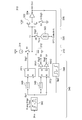
- FIG. 24 is a circuit diagram showing a configuration example of the control circuit 340.
- the control circuit 340 is composed of a logic circuit.
- the control circuit 340 includes a first edge detection circuit 342, a second edge detection circuit 344, a first delay circuit 346, a second delay circuit 348, a first flip-flop FF1, a second flip-flop FF2, a first inverter INV1 and a second inverter INV1.
- the inverter INV2 is included.
- the first edge detection circuit 342 generates a first pulse signal Sp1 having a predetermined pulse width in response to a positive edge (also called a rising edge or a leading edge) of the input signal IN.
- the second edge detection circuit 344 responds to the positive edge of the output signal OUT and generates the second pulse signal Sp2 having a predetermined pulse width.
- the first delay circuit 346 delays the first pulse signal Sp1 by the delay amount ⁇ 1 and supplies the delayed signal to the set terminal (S) of the first flip-flop FF1.
- This delay amount ⁇ 1 guarantees that the third switch S3 is turned on surely and the first switch S1 is turned on after the voltage comparison becomes possible.
- the second pulse signal Sp2 is input to the reset terminal (R) of the first flip-flop FF1. On/off of the first switch S1 is controlled by the output Sig1 of the first flip-flop FF1.
- the second delay circuit 348 delays the second pulse signal S12 by the delay amount ⁇ 2 and supplies it to the set terminal of the second flip-flop FF2. After the capacitor voltage V P reaches the threshold value V TH , there is a delay of two stages of the inverter 332 and the inverter 334 until the output OUT rises completely to high (VDD). Therefore, by introducing the delay amount ⁇ 2 , the third switch S3 can be turned off after the output OUT completely rises to high (VDD).
- the first pulse signal Sp1 is input to the reset terminal of the second flip-flop FF2.
- the second switch S2 and the third switch S3 are controlled based on the state of the second flip-flop FF2. Specifically, the inverted signal Sig3 of the output Q of the second flip-flop FF2 is supplied to the third switch S3, and the inverted signal Sig2 of the inverted output QB of the second flip-flop FF2 is supplied to the second switch S2. ..
- the second flip-flop FF2 is reset at the timing of the negative edge of the first pulse signal Sp1. Therefore, the timing of turning on the second switch S2 and turning off the third switch S3 is defined by the pulse width of the first pulse signal Sp1.
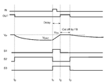
- FIG. 25 is a time chart explaining the operation of the DTC 300 of FIG.
- the second switch S2 is turned on and the capacitor 312 is charged by the DAC 309.
- the voltage V P of the capacitor becomes the voltage value V DAC according to the control code.
- the first switch S1 When the input signal IN transitions to high at time t 1 , the first switch S1 is turned on, the capacitor 312 is charged by the current I C generated by the current source 314, and the voltage V P of the capacitor 312 increases at a constant slope. To do. At this time, the third switch S3 is also turned on, and the inverter 306 is in a state where the voltages can be compared.
- the control circuit 340 turns off the first switch S1. As a result, the charging of the capacitor 312 is stopped. As a result, the voltage V P is maintained near the threshold voltage V TH . Then, at time t 3 after a lapse of time corresponding to the delay amount of the second delay circuit 348, the second switch S2 and the third switch S3 is turned on. The above is the operation of one cycle. Then, the advantage is demonstrated.
- FIG. 26 is a diagram showing an operation waveform (i) of the DTC according to the present embodiment and an operation waveform (ii) of the conventional DTC.
- the variation of the voltage V P of the capacitor 312 is suppressed to the minimum as compared with the conventional case. That is, wasteful supply of electric charges to the capacitor 312 and wasteful discharge of electric charges from the capacitor 312 are reduced, and power consumption can be reduced.
- the first switch S1 is turned on only during the slope generation period. In other words, the current I C generated by the current source 314 is 100%, which is used for generating the slope, and power consumption can be reduced.
- the third switch S3 is arranged on the path of the inverter 306 and is turned on only during the voltage comparison period. As a result, when the output voltage V DAC of the DAC 309 is close to the threshold value V TH of the inverter (comparator) 306, it is possible to prevent a through current from flowing through the inverter 306 and further reduce power consumption.
- the comparison means 330 may be composed of a voltage comparator.
- the switch S3 may be incorporated in the voltage comparator to cut off the bias current of the voltage comparator.
- the present invention can be applied to electronic circuits.
Landscapes
- Engineering & Computer Science (AREA)
- Theoretical Computer Science (AREA)
- Physics & Mathematics (AREA)
- General Engineering & Computer Science (AREA)
- General Physics & Mathematics (AREA)
- Nonlinear Science (AREA)
- Stabilization Of Oscillater, Synchronisation, Frequency Synthesizers (AREA)
Abstract
DTC102は、入力基準クロックREFを受け、第1基準クロックREFAを生成する。遅延回路122は、第1基準クロックREFAを遅延させ、第2基準クロックREFBを生成する。TDC104は、第2基準クロックREFBと、フィードバッククロックFBの位相差をデジタル信号に変換する。DCO108は、TDC104の出力に応じた周波数で発振し、出力クロックOUTを生成する。分周器112Aは、オン、オフが切り替え可能であり、オン状態において、出力クロックCKVを周波数制御ワードFCWに応じた分周比で分周する。第1モードにおいて、フィードバッククロックFBは、分周器112Aの出力を出力クロックCKVでリタイミングした信号であり、第2モードにおいて、フィードバッククロックFBは、第1基準クロックREFAを出力クロックCKVでリタイミングした信号である。
Description
本発明は、デジタル位相同期回路、デジタル制御発振器、デジタル-時間変換器に関する。
基準クロックを逓倍して任意の周波数のクロックを生成するために、位相同期回路(PLL(Phase Locked Loop))が用いられる。PLL回路の一形態として、デジタルPLL回路(D-PLL:Digital PLL)が知られている。
図1は、分数分周型(Fractional-N)のD-PLL回路100Rの基本アーキテクチャを示す回路図である。D-PLL回路100Rは、基準クロックREFと、逓倍数を指定する周波数制御ワード(FCW:Frequency Control Word)を受け、基準クロックREFをFCWに応じて逓倍した出力クロックOUTを生成する。
デジタル-時間変換器(DTC:Digital-To-Time Converter)102、時間-デジタル変換器(TDC:Time-To-Digital Converter)104、デジタルループフィルタ(DLF:Digital Loop Filter)106、デジタル制御発振器(DCO:Digitally-Controlled Oscillator)108、バッファ110、マルチモデュラス分周器(MMD:Multi-Modulous Divider)112、コントローラ114、リタイミング回路116を備える。
DCO108は、デジタルの制御データDCNTに応じた周波数で発振する。DCO108の出力クロックOUTは、バッファ110を経由して、MMD112に入力される。MMD112は、コントローラ114によって設定された分周比で、出力クロックOUTを分周する。コントローラ114は、ΔΣ変調器のアーキテクチャにもとづいて設計される。フラクショナルN型のPLL回路において、コントローラ114は、分数の逓倍比を得るために、MMD112の分周比を、複数の整数値で時分割で切り替える。MMD112に設定される分周比の平均値の逆数が、D-PLL回路100の逓倍比NFとなる。
分周後のクロックDIVは、リタイミング回路116に入力される。リタイミング回路116は、分周クロックDIVを、バッファ110を経由した出力クロックCKVによってリタイミングし、フィードバッククロックFBを生成する。
DTC102は、基準クロックREFに、コントローラ114によって設定された遅延を与え、基準クロックREFAを出力する。この遅延量は、MMD112に与える分周比に応じて選択される。
TDC104は、基準クロックREFAとフィードバッククロックFBの時間差をデジタル値に変換する。DLF106は、TDC104の出力の高周波成分を除去し、制御データDCNTを生成する。
以上がD-PLL回路100Rの基本アーキテクチャである。図2は、図1のD-PLL回路100Rのタイムチャートである。分周クロックDIVは、クロックCKVによってリタイミングされる。リタイミング回路116におけるサンプリング遅延τSAMによって、フィードバッククロックFBのエッジE1は、クロックCKVのエッジE2に対して、τSAMだけ遅延している。TDC104およびDLF106からなるフィードバックループによって、基準クロックREFAのエッジE3とフィードバッククロックFBのエッジE1の時間差がゼロとなるようにフィードバックがかかり、位相がロックされる。このとき、DCO108の出力クロックOUT(およびCKV)の周波数は、基準クロックREFA(およびREF)の周波数の、NF倍となる。
図1のD-PLL回路100Rは、周波数精度が高く、周波数妨害に対して堅牢であるという利点を有する。しかしながら、MMD112およびリタイミング回路116が、高周波数のクロックCKVと同期して動作し続けるため、消費電力が大きいという問題がある。
本発明は係る課題に鑑みてなされたものであり、そのある態様の例示的な目的のひとつは、消費電力が削減されたD-PLL回路の提供にある。
本発明のある態様は、第1基準クロックを受け、出力クロックを生成する位相同期回路に関する。位相同期回路は、第1基準クロックを遅延させ、第2基準クロックを生成する遅延回路と、第2基準クロックと、フィードバッククロックの位相差に応じた制御信号を生成するフィードバック回路と、制御信号に応じた周波数で発振し、出力クロックを生成する発振器と、オン、オフが切り替え可能であり、オン状態において、出力クロックを分周する分周器と、を備える。この位相同期回路は、第1モードと第2モードが切り替え可能であり、第1モードにおいて、フィードバッククロックは、分周器の出力を出力クロックでリタイミングした信号である。第2モードにおいて、フィードバッククロックは、第1基準クロックを出力クロックでリタイミングした信号である。
本発明のある態様は、入力基準クロックと周波数制御ワードを受け、出力クロックを生成するデジタル位相同期回路に関する。デジタル位相同期回路は、入力基準クロックを受け、第1基準クロックを生成するデジタル-時間変換器と、第1基準クロックを遅延させ、第2基準クロックを生成する遅延回路と、第2基準クロックと、フィードバッククロックの位相差をデジタル信号に変換する時間-デジタル変換器と、時間-デジタル変換器の出力に応じた周波数で発振し、出力クロックを生成するデジタル制御発振器と、オン、オフが切り替え可能であり、オン状態において、出力クロックを周波数制御ワードに応じた分周比で分周する分周器と、を備える。第1モードと第2モードが切り替え可能であり、第1モードにおいて、フィードバッククロックは、分周器の出力を出力クロックでリタイミングした信号であり、第2モードにおいて、フィードバッククロックは、第1基準クロックを出力クロックでリタイミングした信号である。
本発明の別の態様は、デジタル制御発振器である。このデジタル制御発振器は、電源ラインと接地ラインの間に縦積みされた上側ユニットと下側ユニットと、上側ユニットと下側ユニットの少なくとも一方と接続される可変キャパシタと、を備える。上側ユニットおよび下側ユニットはそれぞれ、クロスカップルされた回路要素のペアと、回路要素のペアと接続されるインダクタと、を含む。上側ユニットと下側ユニットのインダクタが結合されてトランスが形成される。
本発明のさらに別の態様は、デジタル-時間変換器である。このデジタル-時間変換器は、入力信号を受け、制御コードに応じた遅延を与え、出力信号を生成するデジタル-時間変換器であって、キャパシタと電流源を含み、スロープ電圧を生成するスロープ発生回路と、キャパシタに、制御コードに応じたアナログ電圧を印加するプリチャージ回路と、スロープ電圧をしきい値と比較し、比較結果に応じた出力信号を生成する比較手段と、入力信号と出力信号に応じて、スロープ発生回路およびプリチャージ回路を制御する制御回路と、を備える。制御回路は、(i)プリチャージ期間においてプリチャージ回路をオンとし、(ii)入力信号に応答してスロープ期間に遷移し、スロープ期間においてプリチャージ回路をオフ、スロープ発生回路をオンとし、(iii)出力信号の遷移に応答してスロープ発生回路をオフする動作を繰り返す。
なお、以上の構成要素の任意の組み合わせや本発明の構成要素や表現を、方法、装置、システムなどの間で相互に置換したものもまた、本発明の態様として有効である。
本発明のある態様によれば、消費電力を低減できる。
(実施の形態の概要)
1. 本明細書に開示される一実施の形態は、第1基準クロックを受け、出力クロックを生成する位相同期回路に関する。位相同期回路は、第1基準クロックを遅延させ、第2基準クロックを生成する遅延回路と、第2基準クロックと、フィードバッククロックの位相差に応じた制御信号を生成するフィードバック回路と、制御信号に応じた周波数で発振し、出力クロックを生成する発振器と、オン、オフが切り替え可能であり、オン状態において、出力クロックを分周する分周器と、を備える。この位相同期回路は、第1モードと第2モードが切り替え可能であり、第1モードにおいて、フィードバッククロックは、分周器の出力を出力クロックでリタイミングした信号である。第2モードにおいて、フィードバッククロックは、第1基準クロックを出力クロックでリタイミングした信号である。
1. 本明細書に開示される一実施の形態は、第1基準クロックを受け、出力クロックを生成する位相同期回路に関する。位相同期回路は、第1基準クロックを遅延させ、第2基準クロックを生成する遅延回路と、第2基準クロックと、フィードバッククロックの位相差に応じた制御信号を生成するフィードバック回路と、制御信号に応じた周波数で発振し、出力クロックを生成する発振器と、オン、オフが切り替え可能であり、オン状態において、出力クロックを分周する分周器と、を備える。この位相同期回路は、第1モードと第2モードが切り替え可能であり、第1モードにおいて、フィードバッククロックは、分周器の出力を出力クロックでリタイミングした信号である。第2モードにおいて、フィードバッククロックは、第1基準クロックを出力クロックでリタイミングした信号である。
この態様によると、第2モードを選択することにより、分周器の動作を停止させ、第2基準クロックをフィードバッククロックとして位相同期をかけることにより、消費電力を低減できる。また必要に応じて第1モードを選択することにより、位相同期が外れた場合に、位相同期状態に復帰させることができる。
一実施例において、位相同期回路は、第1モードと第2モードを指示するイネーブル信号を生成するモードコントローラと、分周器の出力と第1基準クロックを受け、イネーブル信号に応じた一方を選択するマルチプレクサと、マルチプレクサの出力を出力クロックによってリタイミングするリタイミング回路と、を備えてもよい。分周器のオン、オフはイネーブル信号に応じて制御され、リタイミング回路の出力がフィードバッククロックであってもよい。
一実施例において、位相同期回路は、第2基準クロックとフィードバッククロックの位相誤差が、デッドゾーンの範囲に含まれるか否かを判定するデッドゾーンディテクタをさらに備え、第1モードと第2モードは、デッドゾーンディテクタの出力に応じていてもよい。これにより、位相同期がかからないモードに陥るのを防止できる。
一実施例において、デッドゾーンディテクタは、第2基準クロックとフィードバッククロックの位相差あるいは周波数差を比較し、比較結果にもとづくパルスを出力する位相周波数検出器と、位相周波数検出器の出力にもとづいて位相誤差を生成し、位相誤差がデッドゾーンに含まれるか否かを判定する判定部と、を含んでもよい。
一実施例において、デジタル位相同期回路は、出力クロックの周波数と、入力基準クロックの周波数の関係を監視し、出力クロックの周波数が、分周器の分周比にもとづいて決まる目標周波数から逸脱する周波数エラーを検出する周波数ロックループをさらに備えてもよい。第1モードと第2モードは、周波数ロックループの出力に応じていてもよい。これにより、誤った周波数で位相ロックがかかるのを防止できる。
周波数ロックループは、入力基準クロックの周期のK倍(Kは整数)の期間、出力クロックをカウントするカウンタを含んでもよい。カウンタのカウント値と、分周比の逆数である逓倍比をK倍した値と、にもとづいて、周波数エラーを検出してもよい。
一実施例において、位相同期回路は、所定のデューティ比を有する制御パルスを生成するデューティサイクルコントローラをさらに備えてもよい。周波数ロックループは、制御パルスに応じて間欠動作してもよい。周波数ロックループを間欠動作させることにより、消費電力の増加を抑制できる。
一実施例において、デジタル位相同期回路は、第2基準クロックとフィードバッククロックの位相差あるいは周波数差を比較し、比較結果にもとづくパルスを出力する位相周波数検出器と、第1モードにおいて動作状態となり、位相周波数検出器の出力にもとづいて、デジタル制御発振器の周波数をフィードバック制御するPLL(Phase Locked Loop)回路と、をさらに備えてもよい。位相周波数検出器とPLL回路を含むフィードバックループの精度は、フィードバック回路の精度より粗くてもよい。これにより、位相ロックが外れた状態からロック状態に素早く引き込むことが可能となる。
位相同期回路は、デジタル位相同期回路であってもよい。フィードバック回路は、第2基準クロックと、フィードバッククロックの位相差をデジタル信号に変換する時間-デジタル変換器を含んでもよい。発振器は、時間-デジタル変換器の出力に応じた周波数で発振するデジタル制御発振器であってもよい。
位相同期回路は分数分周型であってもよい。分周器はマルチモデュラス分周器であってもよい。位相同期回路は、入力基準クロックを受け、第1基準クロックを生成するデジタル-時間変換器と、出力クロックの周波数を指定する周波数制御ワードに応じて、デジタル-時間変換器とマルチモデュラス分周器を制御するコントローラと、をさらに備えてもよい。
2. 本発明の別の態様は、デジタル制御発振器である。このデジタル制御発振器は、電源ラインと接地ラインの間に縦積みされた上側ユニットと下側ユニットと、上側ユニットと下側ユニットの少なくとも一方と接続される可変キャパシタと、を備える。上側ユニットおよび下側ユニットはそれぞれ、クロスカップルされた回路要素のペアと、回路要素のペアと接続されるインダクタと、を含む。上側ユニットと下側ユニットのインダクタが結合されてトランスが形成される。
この構成によれば、トランスによるゲイン増幅の効果によって、同じ振幅を得るためのバイアス電流を減らすことができ、あるいはバイアス電流を維持した場合に振幅を増大できる。
上側ユニットと下側ユニットの少なくとも一方は、回路要素のペアがNMOS(N-channel Metal Oxide Semiconductor)トランジスタであるN型であってもよい。上側ユニットと下側ユニットの両方がN型であってもよい。
上側ユニットと下側ユニットの少なくとも一方は、回路要素のペアがPMOS(P-channel Metal Oxide Semiconductor)トランジスタであるP型であってもよい。
上側ユニットと下側ユニットの少なくとも一方は、回路要素のペアが、CMOS(Complementary Metal Oxide Semiconductor)インバータであるCMOS型であってもよい。
デジタル制御発振器は、電源ラインと接地ラインの間に挿入されたバイアス電流源をさらに備えてもよい。
デジタル制御発振器は、上側ユニットと下側ユニットの接続ノードに接続されるキャパシタをさらに備えてもよい。
3. 本発明のさらに別の態様は、デジタル-時間変換器である。このデジタル-時間変換器は、入力信号を受け、制御コードに応じた遅延を与え、出力信号を生成する。デジタル-時間変換器は、キャパシタと電流源を含み、スロープ電圧を生成するスロープ発生回路と、キャパシタに、制御コードに応じたアナログ電圧を印加するプリチャージ回路と、スロープ電圧をしきい値と比較し、比較結果に応じた出力信号を生成する比較手段と、入力信号と出力信号に応じて、スロープ発生回路およびプリチャージ回路を制御する制御回路と、を備える。制御回路は、(i)プリチャージ期間においてプリチャージ回路をオンとし、(ii)入力信号に応答してスロープ期間に遷移し、スロープ期間においてプリチャージ回路をオフ、スロープ発生回路をオンとし、(iii)出力信号の遷移に応答してスロープ発生回路をオフする動作を繰り返す。
この態様によると、キャパシタへの無駄な充放電を抑制することで、消費電力を低減できる。
比較手段は、オン、オフが切り替え可能に構成され、制御回路は、プリチャージ期間において比較手段をオフしてもよい。
(実施の形態)
以下、本発明を好適な実施の形態をもとに図面を参照しながら説明する。各図面に示される同一または同等の構成要素、部材、処理には、同一の符号を付するものとし、適宜重複した説明は省略する。また、実施の形態は、発明を限定するものではなく例示であって、実施の形態に記述されるすべての特徴やその組み合わせは、必ずしも発明の本質的なものであるとは限らない。
以下、本発明を好適な実施の形態をもとに図面を参照しながら説明する。各図面に示される同一または同等の構成要素、部材、処理には、同一の符号を付するものとし、適宜重複した説明は省略する。また、実施の形態は、発明を限定するものではなく例示であって、実施の形態に記述されるすべての特徴やその組み合わせは、必ずしも発明の本質的なものであるとは限らない。
本明細書において、「部材Aが、部材Bと接続された状態」とは、部材Aと部材Bが物理的に直接的に接続される場合のほか、部材Aと部材Bが、それらの電気的な接続状態に実質的な影響を及ぼさない、あるいはそれらの結合により奏される機能や効果を損なわせない、その他の部材を介して間接的に接続される場合も含む。
同様に、「部材Cが、部材Aと部材Bの間に設けられた状態」とは、部材Aと部材C、あるいは部材Bと部材Cが直接的に接続される場合のほか、それらの電気的な接続状態に実質的な影響を及ぼさない、あるいはそれらの結合により奏される機能や効果を損なわせない、その他の部材を介して間接的に接続される場合も含む。
(D-PLL回路)
図3は、実施の形態に係るD-PLL回路100の基本アーキテクチャを示す回路図である。D-PLL回路100は、分数分周型のPLL回路であり、入力基準クロックREFおよび周波数制御ワードFCWを受け、入力基準クロックREFの周波数Fの分数倍の周波数を有する出力クロックOUTを発生する。
図3は、実施の形態に係るD-PLL回路100の基本アーキテクチャを示す回路図である。D-PLL回路100は、分数分周型のPLL回路であり、入力基準クロックREFおよび周波数制御ワードFCWを受け、入力基準クロックREFの周波数Fの分数倍の周波数を有する出力クロックOUTを発生する。
D-PLL回路100は、図1のD-PLL回路100Rに加えて、マルチプレクサ120、遅延回路122、モードセレクタ130をさらに備える。またMMD112Aは、イネーブル/ディセーブル(オン/オフ)が切り替え可能に構成される。
D-PLL回路100は、2つのモード(サンプリングモードとサブサンプリングモードと称する)が切り替え可能であり、2つのモードは、イネーブル信号ENに応じて選択される。イネーブル信号ENが1(ハイ)のとき、D-PLL回路100はサンプリングモードにセットされ、イネーブル信号ENが0(ロー)のとき、サブサンプリングモードにセットされる。
マルチプレクサ120は、MMD112の出力である分周クロックDIVと、DTC102が出力する第1基準クロックREFAを受け、イネーブル信号ENに応じた一方を選択する。マルチプレクサ120の出力が、リタイミング回路116によって、リタイミングされ、フィードバッククロックFBとなる。リタイミングには、バッファ110を経由した出力クロックCKVを用いることができる。なお、DCO108の出力インピーダンスが十分に低い場合、バッファ110は省略してもよい。
ここではイネーブル信号ENが1(ハイ)のとき、フィードバッククロックFBは分周クロックDIVにもとづいて生成され、0(ロー)のとき第1基準クロックREFAにもとづいてフィードバッククロックFBが生成される。
MMD112Aの機能は、図1のそれと同じであるが、イネーブル信号ENに応じて、オン、オフが切り替え可能に構成される。たとえばMMD112Aは、図1のMMD112に加えてゲート回路113を含む。ゲート回路113は、MMD112の前段に挿入され、イネーブル信号ENに応じて、クロック信号CKVをゲーティングする。すなわち、イネーブル信号ENが1のとき、ゲート回路113を通過したクロックCKGが、MMD112に入力され、MMD112がイネーブルとなる。EN信号が0のとき、クロックCKGはローに固定され、したがってMMD112はディセーブルとなる。
遅延回路122は、DTC102の後段に挿入され、第1基準クロックREFAに、遅延τFBを与え、第2基準クロックREFBを出力する。TDC104は、第2基準クロックREFBのエッジと、フィードバッククロックFBのエッジが一致するように、フィードバックがかかる。
モードセレクタ130は、D-PLL回路100の動作状態にもとづいて、イネーブル信号ENを生成し、D-PLL回路100のモードを制御する。
以上がD-PLL回路100の基本構成である。続いてその動作を説明する。図4は、サブサンプリングモード(EN=0)におけるD-PLL回路100の等価回路図である。サブサンプリングモードでは、MMD112の動作が停止する。第1基準クロックREFAの周波数と、分周クロックDIVの周波数は等しいから、分周クロックDIVに代えて、第1基準クロックREFAがリタイミング回路116に入力される。そして、リタイミング回路116は、クロック信号CKVのエッジで、第1基準クロックREFAをリタイミングし、フィードバッククロックFBを生成する。
図5は、サブサンプリングモードにおけるD-PLL回路100のタイムチャートである。サブサンプリングモードでは、分周クロックDIVに代えて、第1基準クロックREFAが、クロックCKVによってリタイミングされる。リタイミング回路116におけるサンプリング遅延τSAMによって、フィードバッククロックFBのエッジE1は、クロックCKVのエッジE2に対して、τSAMだけ遅延している。TDC104およびDLF106を含むフィードバックループによって、第2基準クロックREFBのエッジE4とフィードバッククロックFBのエッジE1の時間差がゼロとなるようにフィードバックがかかり、位相がロックされる。
サブサンプリングモードでは、フィードバッククロックFBを、第1基準クロックREFAのリタイミングにより生成する関係上、フィードバッククロックFBのエッジは、第1基準クロックREFAのエッジよりも遅れることになる。したがってフィードバックをかけても、フィードバッククロックFBのエッジ(位相)を、第1基準クロックREFAのエッジに揃えることはできない。そこで、リタイミングによりフィードバッククロックFBを生成する際の位相の遅れを考慮して、それを相殺できるように遅延回路122の遅延量τFBを定めることにより、第2基準クロックREFBの位相(=REFA+τFB)と、リタイミングにより遅れたフィードバッククロックFBの位相(=REFA+Δt+τSAM)が、クロック信号CKVの1周期以内に含まれることとなり、位相同期をかけることが可能となる。
図6(a)、(b)は、サンプリングモードとサブサンプリングモードにおけるD-PLL回路100の動作を対比して示すタイムチャートである。図6(a)のサンプリングモードの動作は、図2のそれと同様である。相違点は、フィードバッククロックFBの位相が、第1基準クロックREFAではなく、第2基準クロックREFBの位相を基準としてロックされる点である。図6(b)のサブサンプリングモードの動作は図5と同様である。
以上がD-PLL回路100の動作である。続いてその利点を説明する。D-PLL回路100をサブサンプリングモードで動作させると、MMD112の動作が停止するため、サンプリングモードに比べて消費電力を格段に低減することができる。
なお、サブサンプリングモードは、出力クロックOUTの周波数fOUTが、その目標値(=fREF×N)にロックされた後は、低消費電力で位相同期を維持することができるが、fOUT≠fREF×Nの状態から、fOUT=fREF×Nの状態に遷移させることができない。これはMMD112を使用しないため、逓倍比Nが回路動作に関与しないためである。
そこで、モードセレクタ130によって、D-PLL回路100の動作状態を監視し、起動時や、位相同期が外れた状況では、一時的にイネーブル信号ENをハイ(1)にして、サンプリングモードに設定することにより、fOUT=fREF×Nの状態に遷移させることができる。
以上が実施の形態に係るD-PLL回路100の基本アーキテクチャである。続いて、D-PLL回路100の具体的な実装を、いくつかの実施例を参照して説明する。
はじめに、サブサンプリングモードで生じうる問題を説明する。図7は、サブサンプリングモードにおけるD-PLL回路100の出力周波数fOUTの波形図(シミュレーション)である。fREF=10MHz、N=240+0.5である。位相同期状態では、出力周波数fOUTは、2405MHz(=2.405GHz)に安定化される。
図7には、-1MHz、+6MHz,+11MHzの周波数妨害を注入したときの波形(i)~(iii)が示される。(i)に示すように、-1MHzの周波数妨害が導入された場合は、位相同期状態を維持することができる。
サブサンプリングモードでは、幅が広い第1基準クロックREFAを、クロックCKVでリタイミングすることに起因して、リタイミングに使用されるクロックCKVのエッジが、前後する。そのため、図7の(ii)で示すように、N’=241+0.5の状態で誤ってロックする可能性がある。あるいは、図7の(iii)で示すように、位相同期がかからず、周波数が振動するような状況に陥る可能性がある。
つまり、モードセレクタ130は、D-PLL回路100の状態を監視して、図7の(ii)や(iii)の状況に陥らないように、D-PLL回路100のモードを制御できるように実装する必要がある。
(実施例1)
図8は、実施例1に係るD-PLL回路100Aの回路図である。この実施例においてモードセレクタ130Aは、図7の波形(iii)で示すような、位相同期しない状態を検出可能に構成される。
図8は、実施例1に係るD-PLL回路100Aの回路図である。この実施例においてモードセレクタ130Aは、図7の波形(iii)で示すような、位相同期しない状態を検出可能に構成される。
モードセレクタ130Aは、デッドゾーンディテクタ140およびステートマシン132を含む。デッドゾーンディテクタ140は、REFBとFBの位相誤差tERRが、デッドゾーンtDZの範囲に含まれるか否かを判定し、範囲外であるとき第1レベル(たとえばハイ、1)、範囲内であるとき第2レベル(たとえばロー、0)となる検出信号ODZ(Out of Dead Zone)を生成する。
デッドゾーンディテクタ140の構成は特に限定されないが、たとえば位相周波数検出器(PFD:Phase Frequency Detector)142および判定部144を含む。PFD142は、第2基準クロックREFBとフィードバッククロックFBの位相差あるいは周波数差を比較し、比較結果にもとづく2個のパルス(UPパルス、DNパルス)を出力する。
判定部144は、PFD142の出力UP/DNを受け、それらにもとづいて位相誤差tERRを生成する。そして位相誤差tERRが、デッドゾーンに含まれるか否かを判定し、ODZ信号を出力する。
ステートマシン132は、ODZ信号を、基準クロックREFと同期させて、イネーブル信号ENを生成する。ステートマシン132は、フリップフロップで構成することができる。
以上がD-PLL回路100Aの構成である。続いてその動作を説明する。図9(a)、(b)は、図8のD-PLL回路100Aにおけるモードセレクタ130Aの動作を説明する図である。図9(a)は、デッドゾーンディテクタ140の入出力特性を示す。
図9(b)は、D-PLL回路100A全体の動作を示す。時刻t0より前は、サブサンプリングモードで動作している。何らかの要因で、フィードバッククロックFBと基準クロックREFBの位相誤差tERRがデッドゾーンtDZの範囲から外れると、ODZ信号が周期的にハイとなり、イネーブル信号ENがハイ(1)となる。その結果、サンプリングモードに切り替わる。サンプリングモードで動作すると、位相誤差tERRが小さくなり、時刻t2に、デッドゾーンtDZの範囲内に戻ると、ODZ信号はローに戻る。これによりイネーブル信号ENがローとなって、サブサンプリングモードに移行する。
以上がD-PLL回路100Aの動作である。デッドゾーンディテクタ140を実装してバックグランドで動作させることにより、図7の(iii)のように位相同期できない状況に陥るのを防止できる。
(実施例2)
図10は、実施例2に係るD-PLL回路100Bの回路図である。この実施例において、モードセレクタ130Bは、図7の波形(ii)で示すような、整数倍の周波数ジャンプを検出可能に構成される。
図10は、実施例2に係るD-PLL回路100Bの回路図である。この実施例において、モードセレクタ130Bは、図7の波形(ii)で示すような、整数倍の周波数ジャンプを検出可能に構成される。
モードセレクタ130Bは、デッドゾーンディテクタ140、ステートマシン132に加えて、間欠動作周波数ロックループ(FLL:Frequency Locked Loop)150を備える。間欠動作FLLを、DC-FLL(Duty Cycled FLL)とも表記する。
間欠動作FLL150は、FLL152およびデューティサイクルコントローラ154を含む。
FLL152は、イネーブルとディセーブルが切り替え可能に構成される。FLL152は、イネーブル状態において、クロック信号CKV(OUT)の周波数と、基準クロックREFの周波数の関係を監視し、クロック信号CKVの周波数が、FCWにもとづいて決まる目標周波数から逸脱すると、周波数ロックエラー信号FLEをアサート(たとえばハイ)する。裏を返すと、FLL152は、基準クロックREFの周期が、クロック信号CKVの周期の何倍であるかを監視し、FCWにもとづく逓倍比と一致するか否かを判定する。ステートマシン132は、周波数ロックエラー信号FLEのアサートに応答して、イネーブル信号ENをハイに切り替える。
FLL152の構成は限定されないが、たとえば周波数検出器160、減算器170、比較器172を含む。周波数検出器160は、基準クロックREFの周期の整数倍(この例ではK=4倍)の間、クロック信号CKVをカウントする。周波数ロックした状態では、このカウント値は、FCW(逓倍数)のK倍となる。
周波数検出器160は、分周器162、Dフリップフロップ164、168、カウンタ166を含む。分周器162は、基準クロックREFを1/K分周(K=1/4)する。分周されたクロックは、フリップフロップ164においてクロックCKVと同期される。カウンタ166は、クロックCKVのパルス数をカウントする。フリップフロップ168は、分周器162の出力のタイミングで、カウンタ166のカウント値を取り込む。フリップフロップ168の出力は、基準クロックREFの周期のK倍の期間に、クロックCKVが何個含まれるかを示す。
減算器170は、フリップフロップ168の出力と、その目標値(K×FCW)の差分(周波数誤差)を算出する。比較器172は、減算器170の出力をしきい値と比較し、周波数誤差が許容値を超える場合に、周波数ロックエラー信号FLEをアサートする。
FLL152は高周波信号(fOUT=2.4GHz)で動作するカウンタ166を含むため、常時動作させておくと、消費電力が大きくなる。そこで、デューティサイクルコントローラ154によって、所定のデューティ比を有する制御パルスDCを生成し、この制御パルスDCにもとづいてFLL152を間欠動作させる。たとえばデューティ比は1%以下、たとえば0.5%程度とすることができる。これにより、FLL152の消費電力を削減できる。
以上がD-PLL回路100Bの構成である。続いてその動作を説明する。図11は、D-PLL回路100Bにおけるモードセレクタ130Bの動作を説明する図である。
間欠動作FLL150は、所定の周期でオン、オフを繰り返す。そして、オンの期間において、周波数エラーが検出されると、サンプリングモードに遷移し、周波数ロックするように動作する。
図11には、D-PLL回路100Bの消費電力が示される。間欠動作FLL150の停止期間中の消費電力はたとえば262μWである。間欠動作FLL150の動作期間中は、D-PLL回路100Bの消費電力が跳ね上がる(たとえば762μW)が、デューティ比が0.5%であるとき、平均の消費電力PAVEは265μWであり、わずかに3μWの増加に抑えることができる。
以上がD-PLL回路100Bの動作である。モードセレクタ130Bによれば、整数倍の周波数ジャンプを検出でき、その場合にサンプリングモードで動作させることにより、図7の(ii)のように誤った状態で位相同期し続けるのを防止できる。なお、図10のモードセレクタ130Bは、間欠動作FLL150に加えてデッドゾーンディテクタ140を備えるため、実施例1と同様に、図7(iii)の状態に陥るのも防止することができる。
図12は、図8のD-PLL回路100Bの出力周波数fOUTの波形図(シミュレーション)である。図7と同様に、-1MHz、+6MHz,+11MHzの周波数妨害が注入したときの波形(i)~(iii)が示される。(i)に示すように、-1MHzの周波数妨害が導入された場合は、位相同期状態を維持することができる。
(ii)に示すように、+11MHzの周波数妨害が導入された場合は、間欠動作FLL150デッドゾーンディテクタ140によって異常状態を検出し、サンプリングモードに切り替えることにより、正しい位相同期状態に戻すことができる。なお、波形(ii)において、周波数が高い状態がしばらく持続しているが、これは間欠動作FLL150を間欠動作させることに起因する検出遅延である。
(iii)に示すように、+6MHzの周波数妨害が導入された場合は、デッドゾーンディテクタ140によって異常状態を検出し、サンプリングモードに切り替えることにより、正しい位相同期状態に戻すことができる。
(実施例3)
図13は、実施例3に係るD-PLL回路100Cの回路図である。D-PLL回路100Cには、精度の荒い(Coarse)第2PLL回路180が追加されている。第2PLL回路180には、イネーブル信号ENがハイのときにクロックCKGが供給される。第2PLL回路180は、イネーブル信号ENがハイの期間、つまりサブサンプリングモードにおいて動作状態となり、PFD182の出力(UP/DN)にもとづいて、DCO108の周波数をフィードバック制御する。つまり図13のD-PLL回路100Cは、TDC104およびDLF106を含む精度の高い(Fine)フィードバックループと、PFD182および第2PLL180を含む精度の粗い(Coarse)フィードバックループが並列動作する。PFD182は、モードセレクタ130に内蔵されるPFD142を流用することができる。なお実施例3においてモードセレクタ130の構成は限定されず、実施例1、2あるいはその他の構成を採用することができる。
図13は、実施例3に係るD-PLL回路100Cの回路図である。D-PLL回路100Cには、精度の荒い(Coarse)第2PLL回路180が追加されている。第2PLL回路180には、イネーブル信号ENがハイのときにクロックCKGが供給される。第2PLL回路180は、イネーブル信号ENがハイの期間、つまりサブサンプリングモードにおいて動作状態となり、PFD182の出力(UP/DN)にもとづいて、DCO108の周波数をフィードバック制御する。つまり図13のD-PLL回路100Cは、TDC104およびDLF106を含む精度の高い(Fine)フィードバックループと、PFD182および第2PLL180を含む精度の粗い(Coarse)フィードバックループが並列動作する。PFD182は、モードセレクタ130に内蔵されるPFD142を流用することができる。なお実施例3においてモードセレクタ130の構成は限定されず、実施例1、2あるいはその他の構成を採用することができる。
実施例3によれば、粗い第2PLL180を追加することにより、サブサンプリングモードにおいて、位相の引き込み速度を高速化することができる。
続いてD-PLL回路100の変形例を説明する。
(変形例1)
図10のモードセレクタ130Bからデッドゾーンディテクタ140を省略した回路も、一実施例として有効である。この場合、位相同期がかからないエラーを、別の手法によって対処すればよい。
図10のモードセレクタ130Bからデッドゾーンディテクタ140を省略した回路も、一実施例として有効である。この場合、位相同期がかからないエラーを、別の手法によって対処すればよい。
(変形例2)
実施の形態では、分数分周型(Fractional-N)のPLLについて説明したがその限りでなく、整数分周型(Integer-N)にも本発明は適用可能である。この場合、DTC102とコントローラ114を削除し、MMD112を単なる分周器(Divider)に置き換えればよい。
実施の形態では、分数分周型(Fractional-N)のPLLについて説明したがその限りでなく、整数分周型(Integer-N)にも本発明は適用可能である。この場合、DTC102とコントローラ114を削除し、MMD112を単なる分周器(Divider)に置き換えればよい。
(変形例3)
また本発明は、D-PLL回路のみでなく、アナログPLL回路にも適用可能である。この場合、TDC104、DLF106、DCO108のセットを、位相周波数比較器(PFD)、チャージポンプ回路、アナログループフィルタ、電圧制御発振器(VCO)に置き換えればよい。
また本発明は、D-PLL回路のみでなく、アナログPLL回路にも適用可能である。この場合、TDC104、DLF106、DCO108のセットを、位相周波数比較器(PFD)、チャージポンプ回路、アナログループフィルタ、電圧制御発振器(VCO)に置き換えればよい。
(DCO)
D-PLL回路100において、あるいはその他のアプリケーションにおいて、DCOは重要な要素技術である。図14(a)、(b)は、従来のDCO200Rの回路図である。DCO200Rは、CMOSオシレータであり、入出力がクロスカップルされたインバータのペア202,204と、インバータのペア202,204の出力間に設けられたタンク回路206、インバータのペア202,204にバイアス電流を供給する電流源208を備える。タンク回路206は、インダクタLと可変キャパシタCを含む並列共振回路である。抵抗Rsは、インダクタLの直列抵抗成分である。可変キャパシタCsの容量値は、デジタル制御可能となっており、DCO200Rは、タンク回路206のインピーダンスに応じた発振周波数で発振する。
D-PLL回路100において、あるいはその他のアプリケーションにおいて、DCOは重要な要素技術である。図14(a)、(b)は、従来のDCO200Rの回路図である。DCO200Rは、CMOSオシレータであり、入出力がクロスカップルされたインバータのペア202,204と、インバータのペア202,204の出力間に設けられたタンク回路206、インバータのペア202,204にバイアス電流を供給する電流源208を備える。タンク回路206は、インダクタLと可変キャパシタCを含む並列共振回路である。抵抗Rsは、インダクタLの直列抵抗成分である。可変キャパシタCsの容量値は、デジタル制御可能となっており、DCO200Rは、タンク回路206のインピーダンスに応じた発振周波数で発振する。
図14(b)には、タンク回路206の等価回路が示される。この等価回路における等価並列抵抗RTANKは、RTANK=ωL・Qで与えられる。Qは、図12のLC共振回路のQ値であり、Q=ωL/Rsで表される。
図14(a)のDCO200Rの出力の振幅VAMPは、式(1)で表され、等価並列抵抗RTANKおよびバイアス電流IBIASに比例する。
VAMP≒4/π×RTANK×IBIAS …(1)
VAMP≒4/π×RTANK×IBIAS …(1)
DCO200Rの消費電力を削減するためにはバイアス電流IBIASを減らす必要がある。ところがDCO200Rを安定的に発振させるためには、出力の振幅VAMPをある程度大きくする必要があるため、バイアス電流IBIASの減少と引き換えに、抵抗RTANKを増加させる必要がある。しかしながら、タンク回路206をMMIC(Monolithic Microwave Integrated Circuit)化してCMOS回路と同じチップに集積化する場合、抵抗RTANKのはせいぜい200~1000Ω程度である。
したがって、図14(a)のDCO200Rの消費電力は、タンク回路のインピーダンスによって制約を受けてしまう。以下では、消費電力をさらに低減することが可能な新規なDCOについて説明する。
図15は、実施の形態に係るDCO200の基本アーキテクチャを示す回路図である。DCO200は、上側ユニット210と、下側ユニット220を備える。上側ユニット210は、クロスカップルされた回路要素のペア212,214と、タップT1が設けられたインダクタ(一次巻線)L1と、を含む。インダクタL1は、回路要素のペア212,214の出力の間(入力の間)に接続される。インダクタL1のタップT1は電源VDDと直接接続され、あるいは後述のようにバイアス電流源が接続される。
図15において、回路要素212,214は、NMOSトランジスタであり、NMOSトランジスタのソース同士は、基準ノード216と接続される。
同様に下側ユニット220は、クロスカップルされた回路要素のペア222,224と、タップT2が設けられたインダクタL2(二次巻線)と、を含む。インダクタL2は、回路要素のペア212,214の出力の間(入力の間)に接続される。
下側ユニット220のタップT2は、上側ユニット210の基準ノード216と接続される。この基準ノード216はキャパシタ242と接続され、仮想接地となる。このノードをCENと表記する。
回路要素222,224もまた、NMOSトランジスタであり、NMOSトランジスタのソース同士は共通に接続される。NMOSトランジスタ222,224のソースは、基準ノード226と接続される。基準ノード216にはバイアス電流源240と接続される。
図15の上側ユニット210、下側ユニット220のように、クロスカップルされた回路要素がNMOSトランジスタであるものを、N型ユニットと称する。
上側ユニット210のインダクタL1と、下側ユニット220のインダクタL2は結合されており、トランス230を形成している。インダクタL1の巻線Lsと、インダクタL2の巻線Lpの結合係数をkとする。
上側ユニット210には、可変キャパシタCvが接続される。可変キャパシタCvは、トランス230とともにLCタンク回路を形成しており、DCO200は、可変キャパシタCvの容量値に応じた周波数で発振する。出力の取り出し箇所は特に限定されないが、たとえば、下側ユニット220のNMOSトランジスタ222,224のドレインから取り出してもよい。
以上がDCO200の基本構成である。続いてその動作を説明する。図16は、図15のDCO200の等価回路図である。Nは、受動ゲインであり、結合係数kを用いて、N=k√(Ls/Lp)で表される。
図16において、出力信号OUTPの振幅VAMPは、式(2)で表される。
VAMP≒4/π×IBIAS×RTANKP×GTF …(2)
GTFは、トランス230によるゲインであり、式(3)で表される。
GTF=k2・Ls/Lp+k√(Ls/Lp)+RTANKS/RTANKP …(3)
GTFは、たとえば2以上の値をとることができ、本発明者らが設計した回路ではGTF=4.35であった。
VAMP≒4/π×IBIAS×RTANKP×GTF …(2)
GTFは、トランス230によるゲインであり、式(3)で表される。
GTF=k2・Ls/Lp+k√(Ls/Lp)+RTANKS/RTANKP …(3)
GTFは、たとえば2以上の値をとることができ、本発明者らが設計した回路ではGTF=4.35であった。
図17は、バイアス電流IBIASと出力信号の振幅VAMPの関係を示す図(シミュレーション)である。(i)は、図15のDCO200の特性を、(ii)は、従来のDCO200Rの特性を示す。同じバイアス電流で比較すると、図15のDCO200によれば、従来比で46%も振幅を大きくできる。言い換えれば、同じ振幅を得るために必要なバイアス電流を大幅に削減できる。
続いてDCO200の変形例を説明する。
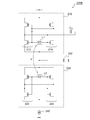
図18は、変形例1に係るDCO200Aの回路図である。この変形例1では、下側ユニット220は、図15の下側ユニット220と同様にN型であるが、上側ユニット210がP型ユニットに置換されている。
P型ユニットは、N型ユニットにおける回路要素212,214のペアをPMOSトランジスタに置換して、天地を反転した構成である。具体的にはインダクタL1は、PMOSトランジスタ212,214のドレインの間に接続され、インダクタL1のタップが仮想接地ラインCENと接続される。またPMOSトランジスタ212,214のソースが基準ノード216となり、電源電圧VDDが供給される。
図19は、変形例2に係るDCO200Bの回路図である。この変形例2では、上側ユニット210および下側ユニット220が、CMOS型(プッシュプル型)ユニットで構成される。
CMOS型ユニットは、クロスカップルされる回路要素のペアが、CMOSインバータである。またインダクタLのタップは省略することができる。
図20(a)~(f)は、DCO200のさらなる変形例を示す回路図である。図20(a)~(f)において、NはN型ユニットを、PはP型ユニットを、CはCMOS型ユニットを表す。
上側ユニット210と下側ユニット220の組み合わせは、上述のそれらに限定されない。図20(a)は、上側ユニット210がCMOS型、下側ユニット220がNMOS型である。図20(b)は、上側ユニット210、下側ユニット220がともにPMOS型である。図20(c)は、上側ユニット210がNMOS型、下側ユニット220がCMOS型である。図20(d)は、上側ユニット210がPMOS型、下側ユニット220がCMOS型である。
図20(e)に示すように、バイアス電流源240を省略してもよいし、図20(f)に示すように電源側に設けてもよい。
またDCO200の出力信号は、上側ユニット210側から取り出してもよいし、下側ユニット220側から取り出してもよい。また可変キャパシタCvを、下側ユニット220側に接続してもよい。
(TDC)
D-PLL回路100において、あるいはその他のアプリケーションにおいて、デジタル-時間変換器(DTC)もまた重要な要素技術である。
D-PLL回路100において、あるいはその他のアプリケーションにおいて、デジタル-時間変換器(DTC)もまた重要な要素技術である。
図21は、従来のDTC300Rの回路図である。このDTC300Rは、シングルスロープ(Single Slope)DTCと称される。DTC300Rは、充電回路302、キャパシタ304、スイッチS1~S3、インバータ306,308、DAC(D/Aコンバータ)309を備える。DTC300Rは、入力信号INに、デジタルの制御コードCODEに応じた遅延を与え、出力する。DAC309は、制御コードCODEに応じたアナログ電圧VDACを出力する。充電回路302は、第1スイッチS1がオンの状態においてキャパシタ304を充電する。インバータ306は、キャパシタ304の電圧VPを、しきい値VTH(=VDD/2)と比較する比較手段として機能する。第3スイッチS3は、オン状態において、キャパシタ304を放電し、電圧VPを初期化する。
図22は、図21のDTC300Rの動作波形図である。時刻t0に、第3スイッチS3がオンとなりキャパシタ304が放電され、電圧VPが初期化される。
時刻t1に第2スイッチS2がオンとなり、キャパシタ304がDAC309の出力電圧VDACによって充電される。これによりVP=VDACとなる。
時刻t2に、入力信号INに応答して、第1スイッチS1がオンとなる。その結果、充電回路302の電流ICによってキャパシタ304が充電され、電圧VPがリニアに増大する。
時刻t3に、電圧VPがしきい値VTHに達すると、出力OUTが変化する。入力INに対する出力OUTの遅延量τは、
τ=(VTH-VDAC)×C/IC
となる。Cはキャパシタ304の容量である。
τ=(VTH-VDAC)×C/IC
となる。Cはキャパシタ304の容量である。
本発明者は、図21のDTC300Rについて検討した結果、以下の課題を認識するに至った。
すなわち、図22のタイムチャートから分かるように、充電回路302が生成する電流のうち、遅延Delayに寄与するのは一部分だけであり、残りは無駄となっている。本発明者らが検討したところ、期間T1とT2において、電流源により58%もの電力が消費されている。
言い換えれば、DTC300Rには、消費電力削減の余地があるといえる。以下では、消費電力を削減したDTCについて説明する。
図23は、実施の形態に係るDTC300の回路図である。DTC300は、スロープ発生回路310、プリチャージ回路320、比較手段330、制御回路340を備える。
スロープ発生回路310は、キャパシタ312、電流源314および第1スイッチS1を含む。電流源314は、キャパシタ312に定電流Icを供給し、キャパシタ312に、一定の傾きで変化するスロープ電圧VPを発生させる。第1スイッチS1は、定電流Icをカットオフするために設けられる。第1スイッチS1は、電流源314の内部に組み込んでもよい。
プリチャージ回路320は、キャパシタ312に、制御コードCODEに応じたアナログ電圧VDACを印加する。プリチャージ回路320は、D/Aコンバータ322と第2スイッチS2を含む。第2スイッチS2がオンのとき、D/Aコンバータ322の出力電圧VDACがキャパシタ312に印加され、第2スイッチS2がオフのとき、キャパシタ312はキャパシタ312から切り離される。なおD/Aコンバータ322が、出力がハイインピーダンスの状態を取り得る場合、第2スイッチS2は省略し、D/Aコンバータ322を制御することで、第2スイッチS2がオフの状態を実現してもよい。
比較手段330は、キャパシタ312に生ずるスロープ電圧VPをしきい値VTHと比較し、比較結果に応じた出力信号OUTを生成する。比較手段330は、カスケードに接続された二段のインバータ332,334を含んでもよい。初段のインバータ332によって、スロープ電圧VPがインバータ332のしきい値と比較され、比較結果に応じた2値の信号に変換される。後段のインバータ332は、信号の論理値を変換し、および/または負荷を駆動するのに十分な低インピーダンスを提供するために設けられている。
好ましくは比較手段330は、オン、オフが切り替え可能に構成され、そのために第3スイッチS3が設けられる。第3スイッチS3は、インバータ332と接地の間に設けられる。第3スイッチS3は、電源ライン側に挿入してもよい。
制御回路340は、入力信号INと出力信号OUTに応じて、スロープ発生回路310およびプリチャージ回路320を制御する。
制御回路340は、プリチャージ期間においてプリチャージ回路320をオンとする。具体的には第2スイッチS2をオンとする。これにより、キャパシタ312が、電圧VDACにより充電される。プリチャージ期間の長さは、D/Aコンバータ322の出力インピーダンスとキャパシタ312の容量Cに応じて決まる時定数、言い換えれば充電に要する時間を考慮して決めればよい。
また制御回路340は、プリチャージ期間において比較手段330をオフする。具体的には第3スイッチS3をオフとする。
また制御回路340は、入力信号INに応答してスロープ期間に遷移する。制御回路340は、スロープ期間においてプリチャージ回路320をオフ、スロープ発生回路310をオンとする。具体的には、第2スイッチS2をオフ、第1スイッチS1をオン、第3スイッチS3をオフとする。
スロープ期間において、スロープ発生回路310がオンとなると、スロープ電圧VPが一定の傾きで変化する。そしてスロープ電圧VPがしきい値VTHとクロスすると、出力信号OUTが遷移する。
制御回路340は、出力信号OUTの遷移に応答してスロープ発生回路310をオフし、定電流ICを遮断する。制御回路340はこの一連の動作を繰り返す。
図24は、制御回路340の構成例を示す回路図である。制御回路340はロジック回路で構成される。制御回路340は、第1エッジ検出回路342、第2エッジ検出回路344、第1遅延回路346、第2遅延回路348、第1フリップフロップFF1、第2フリップフロップFF2、第1インバータINV1、第2インバータINV2を含む。
第1エッジ検出回路342は、入力信号INのポジエッジ(立ち上がりエッジ、リーディングエッジともいう)に応答し、所定のパルス幅を有する第1パルス信号Sp1を生成する。第2エッジ検出回路344は、出力信号OUTのポジエッジに応答し、所定のパルス幅を有する第2パルス信号Sp2を生成する。
第1遅延回路346は、第1パルス信号Sp1を遅延量τ1だけ遅延し、遅延後の信号を第1フリップフロップFF1のセット端子(S)に供給する。この遅延量τ1によって、第3スイッチS3が確実にオンとなり、電圧比較が可能な状態になってから、第1スイッチS1がオンとなることが保証される。また第1フリップフロップFF1のリセット端子(R)には、第2パルス信号Sp2が入力される。第1スイッチS1のオン、オフは、第1フリップフロップFF1の出力Sig1によって制御される。
第2遅延回路348は、第2パルス信号S12を遅延量τ2だけ遅延し、第2フリップフロップFF2のセット端子に供給する。キャパシタ電圧VPがしきい値VTHに達した後、出力OUTが完全にハイ(VDD)に立ち上がるまでには、インバータ332およびインバータ334の二段分の遅延がある。そこで、遅延量τ2を導入することにより、出力OUTが完全にハイ(VDD)に立ち上がってから、第3スイッチS3をオフすることができる。
また第2フリップフロップFF2のリセット端子には、第1パルス信号Sp1が入力される。第2スイッチS2および第3スイッチS3は、第2フリップフロップFF2の状態にもとづいて制御される。具体的には、第2フリップフロップFF2の出力Qの反転信号Sig3が、第3スイッチS3に供給され、第2フリップフロップFF2の反転出力QBの反転信号Sig2が、第2スイッチS2に供給される。
第2フリップフロップFF2は、第1パルス信号Sp1のネガエッジのタイミングでリセットされる。したがって、第2スイッチS2がオン、第3スイッチS3がオフするタイミングは、第1パルス信号Sp1のパルス幅で規定される。
以上がDTC300の構成である。続いてその動作を説明する。図25は、図23のDTC300の動作を説明するタイムチャートである。
時刻t0に、第2スイッチS2がオンとなり、キャパシタ312が、DAC309によって充電される。これによりキャパシタの電圧VPは、制御コードに応じた電圧値VDACとなる。
時刻t1に、入力信号INがハイに遷移すると、第1スイッチS1がオンとなり、キャパシタ312が電流源314が生成する電流ICによって充電され、キャパシタ312の電圧VPが一定の傾きで増大する。このとき、第3スイッチS3もオンとなり、インバータ306が電圧比較可能な状態となる。
時刻t2に、電圧VPがしきい値VTHに達すると、出力OUTがハイに遷移する。これに応答して、制御回路340は、第1スイッチS1をオフする。その結果、キャパシタ312への充電が停止する。その結果、電圧VPは、しきい値電圧VTHの近傍に維持される。その後、第2遅延回路348の遅延量に相当する時間の経過後の時刻t3に、第2スイッチS2および第3スイッチS3がオンとなる。以上が1サイクルの動作である。続いてその利点を説明する。
図26は、本実施の形態に係るDTCの動作波形(i)と、従来のDTCの動作波形(ii)を示す図である。本実施の形態では、従来に比べて、キャパシタ312の電圧VPの変動が最小限に抑制されている。つまり、キャパシタ312に対する電荷の無駄な供給、キャパシタ312からの電荷の無駄な放出が削減され、消費電力を削減できる。特に、本実施の形態において、第1スイッチS1は、スロープ発生期間のみオンとなる。言い換えれば電流源314が生成する電流ICは100%、スロープの生成に使用されることとなり、消費電力を削減できる。
また、第3スイッチS3をインバータ306の経路上に配置し、電圧比較の期間のみオンすることとした。これにより、DAC309の出力電圧VDACがインバータ(コンパレータ)306のしきい値VTHに近いときに、インバータ306に貫通電流が流れるのを防止でき、さらに消費電力を削減できる。
図23において、比較手段330を電圧コンパレータで構成してもよい。この場合、スイッチS3を電圧コンパレータに組み込んで、電圧コンパレータのバイアス電流を遮断するようにしてもよい。
実施の形態にもとづき、具体的な用語を用いて本発明を説明したが、実施の形態は、本発明の原理、応用を示しているにすぎず、実施の形態には、請求の範囲に規定された本発明の思想を逸脱しない範囲において、多くの変形例や配置の変更が認められる。
本発明は、電子回路に利用できる。
100 D-PLL回路
102 DTC
104 TDC
106 DLF
108 DCO
110 バッファ
112 MMD
113 ゲート回路
114 コントローラ
116 リタイミング回路
120 マルチプレクサ
122 遅延回路
130 モードセレクタ
132 ステートマシン
140 デッドゾーンディテクタ
142 PFD
144 判定部
150 間欠動作FLL
152 FLL
154 デューティサイクルコントローラ
160 周波数検出器
162 分周器
164 フリップフロップ
166 カウンタ
168 フリップフロップ
170 減算器
172 比較器
180 第2PLL
200 DCO
210 上側ユニット
220 下側ユニット
230 トランス
300 DTC
310 スロープ発生回路
312 キャパシタ
314 電流源
S1 第1スイッチ
320 プリチャージ回路
322 D/Aコンバータ
S2 第2スイッチ
330 比較手段
332,334 インバータ
340 制御回路
342 第1エッジ検出回路
344 第2エッジ検出回路
346 第1遅延回路
348 第2遅延回路
FF1 第1フリップフロップ
FF2 第2フリップフロップ
INV1 第1インバータ
INV2 第2インバータ
102 DTC
104 TDC
106 DLF
108 DCO
110 バッファ
112 MMD
113 ゲート回路
114 コントローラ
116 リタイミング回路
120 マルチプレクサ
122 遅延回路
130 モードセレクタ
132 ステートマシン
140 デッドゾーンディテクタ
142 PFD
144 判定部
150 間欠動作FLL
152 FLL
154 デューティサイクルコントローラ
160 周波数検出器
162 分周器
164 フリップフロップ
166 カウンタ
168 フリップフロップ
170 減算器
172 比較器
180 第2PLL
200 DCO
210 上側ユニット
220 下側ユニット
230 トランス
300 DTC
310 スロープ発生回路
312 キャパシタ
314 電流源
S1 第1スイッチ
320 プリチャージ回路
322 D/Aコンバータ
S2 第2スイッチ
330 比較手段
332,334 インバータ
340 制御回路
342 第1エッジ検出回路
344 第2エッジ検出回路
346 第1遅延回路
348 第2遅延回路
FF1 第1フリップフロップ
FF2 第2フリップフロップ
INV1 第1インバータ
INV2 第2インバータ
Claims (21)
- 第1基準クロックを受け、出力クロックを生成する位相同期回路であって、
前記第1基準クロックを遅延させ、第2基準クロックを生成する遅延回路と、
前記第2基準クロックと、フィードバッククロックの位相差に応じた制御信号を生成するフィードバック回路と、
前記制御信号に応じた周波数で発振し、前記出力クロックを生成する発振器と、
オン、オフが切り替え可能であり、オン状態において、前記出力クロックを分周する分周器と、
を備え、
第1モードと第2モードが切り替え可能であり、前記第1モードにおいて、前記フィードバッククロックは、前記分周器の出力を前記出力クロックでリタイミングした信号であり、前記第2モードにおいて、前記フィードバッククロックは、前記第1基準クロックを前記出力クロックでリタイミングした信号であることを特徴とする位相同期回路。 - 前記第1モードと前記第2モードを指示するイネーブル信号を生成するモードコントローラと、
前記分周器の出力と前記第1基準クロックを受け、前記イネーブル信号に応じた一方を選択するマルチプレクサと、
前記マルチプレクサの出力を前記出力クロックによってリタイミングするリタイミング回路と、
を備え、前記分周器のオン、オフは前記イネーブル信号に応じて制御され、前記リタイミング回路の出力が前記フィードバッククロックであることを特徴とする請求項1に記載の位相同期回路。 - 前記第2基準クロックと前記フィードバッククロックの位相誤差が、デッドゾーンの範囲に含まれるか否かを判定するデッドゾーンディテクタをさらに備え、前記第1モードと前記第2モードは、前記デッドゾーンディテクタの出力に応じていることを特徴とする請求項1または2に記載の位相同期回路。
- 前記デッドゾーンディテクタは、
前記第2基準クロックと前記フィードバッククロックの位相差あるいは周波数差を比較し、比較結果にもとづくパルスを出力する位相周波数検出器と、
前記位相周波数検出器の出力にもとづいて前記位相誤差を生成し、前記位相誤差が前記デッドゾーンに含まれるか否かを判定する判定部と、
を含むことを特徴とする請求項3に記載の位相同期回路。 - 前記出力クロックの周波数と、前記入力基準クロックの周波数の関係を監視し、前記出力クロックの周波数が前記分周比にもとづいて決まる目標周波数から逸脱する周波数エラーを検出する周波数ロックループをさらに備え、
前記第1モードと前記第2モードは、前記周波数ロックループの出力に応じていることを特徴とする請求項1から4のいずれかに記載の位相同期回路。 - 前記周波数ロックループは、
前記入力基準クロックの周期のK倍(Kは整数)の期間、前記出力クロックをカウントするカウンタを含み、
前記カウンタのカウント値と、前記分周比の逆数である逓倍比をK倍した値と、にもとづいて、前記周波数エラーを検出することを特徴とする請求項5に記載の位相同期回路。 - 所定のデューティ比を有する制御パルスを生成するデューティサイクルコントローラをさらに備え、
前記周波数ロックループは、前記制御パルスに応じて間欠動作することを特徴とする請求項6に記載の位相同期回路。 - 前記第2基準クロックと前記フィードバッククロックの位相差あるいは周波数差を比較し、比較結果にもとづくパルスを出力する位相周波数検出器と、
前記第1モードにおいて動作状態となり、前記位相周波数検出器の出力にもとづいて、前記発振器の周波数をフィードバック制御するPLL(Phase Locked Loop)回路と、
をさらに備え、
前記位相周波数検出器と前記PLL回路を含むフィードバックループの精度は、前記フィードバック回路の精度より粗いことを特徴とする請求項1から7のいずれかに記載の位相同期回路。 - 前記位相同期回路は、デジタル位相同期回路であり、
前記フィードバック回路は、前記第2基準クロックと、フィードバッククロックの位相差をデジタル信号に変換する時間-デジタル変換器を含み、
前記発振器は、前記時間-デジタル変換器の出力に応じた周波数で発振するデジタル制御発振器であることを特徴とする請求項1から8のいずれかに記載の位相同期回路。 - 前記デジタル制御発振器は、
電源ラインと接地ラインの間に縦積みされた上側ユニットと下側ユニットと、
前記上側ユニットと前記下側ユニットの少なくとも一方と接続される可変キャパシタと、
を備え、
前記上側ユニットおよび前記下側ユニットはそれぞれ、
クロスカップルされた回路要素のペアと、
前記回路要素のペアと接続されるインダクタと、
を含み、
前記上側ユニットと前記下側ユニットのインダクタが結合されてトランスが形成されることを特徴とする請求項9に記載の位相同期回路。 - 前記位相同期回路は分数分周型であり、
前記分周器はマルチモデュラス分周器であり、
前記位相同期回路は、
入力基準クロックを受け、前記第1基準クロックを生成するデジタル-時間変換器と、
前記出力クロックの周波数を指定する周波数制御ワードに応じて、前記デジタル-時間変換器と前記マルチモデュラス分周器を制御するコントローラと、
をさらに備えることを特徴とする請求項9または10に記載の位相同期回路。 - 前記デジタル-時間変換器は、
キャパシタと電流源を含み、スロープ電圧を生成するスロープ発生回路と、
前記キャパシタに、制御コードに応じたアナログ電圧を印加するプリチャージ回路と、
前記スロープ電圧をしきい値と比較し、比較結果に応じた前記第1基準クロックを生成する比較手段と、
前記入力基準クロックと前記第1基準クロックに応じて、前記スロープ発生回路および前記プリチャージ回路を制御する制御回路と、
を備え、
前記制御回路は、(i)プリチャージ期間において前記プリチャージ回路をオンとし、(ii)前記入力基準クロックに応答してスロープ期間に遷移し、前記スロープ期間において前記プリチャージ回路をオフ、前記スロープ発生回路をオンとし、(iii)前記第1基準クロックの遷移に応答して前記スロープ発生回路をオフする動作を繰り返すことを特徴とする請求項11に記載の位相同期回路。 - 電源ラインと接地ラインの間に縦積みされた上側ユニットと下側ユニットと、
前記上側ユニットと前記下側ユニットの少なくとも一方と接続される可変キャパシタと、
を備え、
前記上側ユニットおよび前記下側ユニットはそれぞれ、
クロスカップルされた回路要素のペアと、
前記回路要素のペアと接続されるインダクタと、
を含み、
前記上側ユニットと前記下側ユニットのインダクタが結合されてトランスが形成されることを特徴とするデジタル制御発振器。 - 前記上側ユニットと前記下側ユニットの少なくとも一方は、前記回路要素のペアがNMOS(N-channel Metal Oxide Semiconductor)トランジスタであるN型であることを特徴とする請求項13に記載のデジタル制御発振器。
- 前記上側ユニットと前記下側ユニットの両方がN型であることを特徴とする請求項14に記載のデジタル制御発振器。
- 前記上側ユニットと前記下側ユニットの少なくとも一方は、前記回路要素のペアがPMOS(P-channel Metal Oxide Semiconductor)トランジスタであるP型であることを特徴とする請求項13に記載のデジタル制御発振器。
- 前記上側ユニットと前記下側ユニットの少なくとも一方は、前記回路要素のペアが、CMOS(Complementary Metal Oxide Semiconductor)インバータであるCMOS型であることを特徴とする請求項13に記載のデジタル制御発振器。
- 前記電源ラインと前記接地ラインの間に挿入されたバイアス電流源をさらに備えることを特徴とする請求項13から17のいずれかに記載のデジタル制御発振器。
- 前記上側ユニットと前記下側ユニットの接続ノードに接続されるキャパシタをさらに備えることを特徴とする請求項13から18のいずれかに記載のデジタル制御発振器。
- 入力信号を受け、制御コードに応じた遅延を与え、出力信号を生成するデジタル-時間変換器であって、
キャパシタと電流源を含み、スロープ電圧を生成するスロープ発生回路と、
前記キャパシタに、制御コードに応じたアナログ電圧を印加するプリチャージ回路と、
前記スロープ電圧をしきい値と比較し、比較結果に応じた前記出力信号を生成する比較手段と、
前記入力信号と前記出力信号に応じて、前記スロープ発生回路および前記プリチャージ回路を制御する制御回路と、
を備え、
前記制御回路は、(i)プリチャージ期間において前記プリチャージ回路をオンとし、(ii)前記入力信号に応答してスロープ期間に遷移し、前記スロープ期間において前記プリチャージ回路をオフ、前記スロープ発生回路をオンとし、(iii)前記出力信号の遷移に応答して前記スロープ発生回路をオフする動作を繰り返すことを特徴とするデジタル-時間変換器。 - 前記比較手段は、オン、オフが切り替え可能に構成され、前記制御回路は、前記プリチャージ期間において前記比較手段をオフすることを特徴とする請求項20に記載のデジタル-時間変換器。
Priority Applications (4)
| Application Number | Priority Date | Filing Date | Title |
|---|---|---|---|
| JP2020572297A JP7501375B2 (ja) | 2019-02-15 | 2020-02-13 | 位相同期回路 |
| US17/400,851 US11962314B2 (en) | 2019-02-15 | 2021-08-12 | Digital phase locked loop circuit, digitally-controlled oscillator, and digital-to-time converter |
| JP2024037924A JP7729422B2 (ja) | 2019-02-15 | 2024-03-12 | デジタル制御発振器 |
| JP2025098015A JP2025128312A (ja) | 2019-02-15 | 2025-06-11 | デジタル-時間変換器 |
Applications Claiming Priority (2)
| Application Number | Priority Date | Filing Date | Title |
|---|---|---|---|
| JP2019-025792 | 2019-02-15 | ||
| JP2019025792 | 2019-02-15 |
Related Child Applications (1)
| Application Number | Title | Priority Date | Filing Date |
|---|---|---|---|
| US17/400,851 Continuation US11962314B2 (en) | 2019-02-15 | 2021-08-12 | Digital phase locked loop circuit, digitally-controlled oscillator, and digital-to-time converter |
Publications (1)
| Publication Number | Publication Date |
|---|---|
| WO2020166645A1 true WO2020166645A1 (ja) | 2020-08-20 |
Family
ID=72045349
Family Applications (1)
| Application Number | Title | Priority Date | Filing Date |
|---|---|---|---|
| PCT/JP2020/005456 Ceased WO2020166645A1 (ja) | 2019-02-15 | 2020-02-13 | デジタル位相同期回路、デジタル制御発振器、デジタル-時間変換器 |
Country Status (3)
| Country | Link |
|---|---|
| US (1) | US11962314B2 (ja) |
| JP (3) | JP7501375B2 (ja) |
| WO (1) | WO2020166645A1 (ja) |
Cited By (4)
| Publication number | Priority date | Publication date | Assignee | Title |
|---|---|---|---|---|
| US20210126766A1 (en) * | 2018-07-10 | 2021-04-29 | Socionext Inc. | Phase synchronization circuit, transmission and reception circuit, and integrated circuit |
| WO2022163683A1 (ja) * | 2021-01-28 | 2022-08-04 | ソニーセミコンダクタソリューションズ株式会社 | 半導体集積回路 |
| JP2024501878A (ja) * | 2020-12-31 | 2024-01-16 | テキサス インスツルメンツ インコーポレイテッド | フィードバック分周器のない低電力フラクショナルアナログpll |
| CN117498840A (zh) * | 2023-12-29 | 2024-02-02 | 中茵微电子(南京)有限公司 | 一种在单端模拟占空比调整器中的并联的粗细调装置 |
Families Citing this family (9)
| Publication number | Priority date | Publication date | Assignee | Title |
|---|---|---|---|---|
| CN114859341B (zh) * | 2021-02-03 | 2023-05-05 | 上海禾赛科技有限公司 | 同步电路、数据处理芯片及雷达 |
| JP7643994B2 (ja) * | 2021-12-22 | 2025-03-11 | ルネサスエレクトロニクス株式会社 | 半導体装置 |
| US12184292B2 (en) * | 2022-07-22 | 2024-12-31 | The Regents Of The University Of Michigan | Sub-sampling phase locked loop (SSPLL) with saturated reference feedback |
| FR3140499A1 (fr) * | 2022-10-03 | 2024-04-05 | Commissariat à l'Energie Atomique et aux Energies Alternatives | Convertisseur analogique-durée |
| US12107588B2 (en) * | 2022-12-06 | 2024-10-01 | Silicon Laboratories Inc. | Maintaining phase coherence for a fractional-N PLL |
| US11923857B1 (en) * | 2023-01-26 | 2024-03-05 | Xilinx, Inc. | DTC nonlinearity correction |
| US12261611B2 (en) * | 2023-07-16 | 2025-03-25 | Cirrus Logic, Inc. | Clock signal transitioning for multi-mode audio processing systems |
| US12306661B2 (en) * | 2023-08-24 | 2025-05-20 | Realtek Semiconductor Corp. | Apparatus and method of power efficient high-speed clock transmission |
| US20250183898A1 (en) * | 2023-11-30 | 2025-06-05 | Texas Instruments Incorporated | Clock and data recovery circuitry |
Citations (4)
| Publication number | Priority date | Publication date | Assignee | Title |
|---|---|---|---|---|
| JP2008054323A (ja) * | 2002-06-03 | 2008-03-06 | Matsushita Electric Ind Co Ltd | 半導体集積回路 |
| US20110273210A1 (en) * | 2010-05-07 | 2011-11-10 | Krishnasawamy Nagaraj | Low power digital phase lock loop circuit |
| JP2013042358A (ja) * | 2011-08-16 | 2013-02-28 | Kawasaki Microelectronics Inc | 周波数シンセサイザ |
| JP2013058881A (ja) * | 2011-09-08 | 2013-03-28 | Japan Radio Co Ltd | Pll回路 |
Family Cites Families (16)
| Publication number | Priority date | Publication date | Assignee | Title |
|---|---|---|---|---|
| US6225871B1 (en) * | 2000-02-07 | 2001-05-01 | Prominenet Communications, Inc. | Voltage controlled CMOS oscillator |
| CN1314205C (zh) | 2002-06-03 | 2007-05-02 | 松下电器产业株式会社 | 半导体集成电路 |
| US20050195917A1 (en) | 2004-03-05 | 2005-09-08 | Texas Instruments Incorporated | Method and apparatus for crystal drift compensation |
| TW200822528A (en) * | 2006-11-07 | 2008-05-16 | Univ Nat Taiwan Science Tech | Multi-phase voltage-control osillator |
| WO2011073853A1 (en) * | 2009-12-17 | 2011-06-23 | Stmicroelectronics S.R.L. | Circuit arrangement of a voltage controlled oscillator |
| TWI418138B (zh) * | 2010-09-15 | 2013-12-01 | Univ Nat Taiwan Science Tech | 注入鎖定除頻裝置 |
| US9306614B2 (en) * | 2013-03-26 | 2016-04-05 | Stmicroelectronics S.R.L. | Power oscillator apparatus with transformer-based power combining for galvanically-isolated bidirectional data communication and power transfer |
| US9041477B2 (en) * | 2013-06-14 | 2015-05-26 | Taiwan Semiconductor Manufacturing Co., Ltd. | Voltage-controlled oscillator |
| US9531394B1 (en) * | 2015-06-22 | 2016-12-27 | Silicon Laboratories Inc. | Calibration of digital-to-time converter |
| US9740175B2 (en) * | 2016-01-18 | 2017-08-22 | Marvell World Trade Ltd. | All-digital phase locked loop (ADPLL) including a digital-to-time converter (DTC) and a sampling time-to-digital converter (TDC) |
| US10135452B2 (en) * | 2017-02-21 | 2018-11-20 | Infineon Technologies Ag | Digital frequency synthesizer with robust injection locked divider |
| US10367452B2 (en) * | 2017-03-16 | 2019-07-30 | Infineon Technologies Ag | System and method for a dual-core VCO |
| KR102419641B1 (ko) * | 2017-03-16 | 2022-07-12 | 삼성전자주식회사 | 디지털-타임 컨버터 및 디지털-타임 컨버터의 동작 방법 |
| EP3407497B1 (en) * | 2017-05-22 | 2024-01-17 | Stichting IMEC Nederland | Digital phase-locked loops using digital-to-time converters |
| JP7193914B2 (ja) * | 2017-11-17 | 2022-12-21 | ローム株式会社 | 可変遅延回路、pll周波数シンセサイザ、電子機器 |
| US10826334B2 (en) * | 2018-03-29 | 2020-11-03 | Silicon Laboratories Inc. | Electromagnetic radiation control for isolated power transfer product |
-
2020
- 2020-02-13 WO PCT/JP2020/005456 patent/WO2020166645A1/ja not_active Ceased
- 2020-02-13 JP JP2020572297A patent/JP7501375B2/ja active Active
-
2021
- 2021-08-12 US US17/400,851 patent/US11962314B2/en active Active
-
2024
- 2024-03-12 JP JP2024037924A patent/JP7729422B2/ja active Active
-
2025
- 2025-06-11 JP JP2025098015A patent/JP2025128312A/ja active Pending
Patent Citations (4)
| Publication number | Priority date | Publication date | Assignee | Title |
|---|---|---|---|---|
| JP2008054323A (ja) * | 2002-06-03 | 2008-03-06 | Matsushita Electric Ind Co Ltd | 半導体集積回路 |
| US20110273210A1 (en) * | 2010-05-07 | 2011-11-10 | Krishnasawamy Nagaraj | Low power digital phase lock loop circuit |
| JP2013042358A (ja) * | 2011-08-16 | 2013-02-28 | Kawasaki Microelectronics Inc | 周波数シンセサイザ |
| JP2013058881A (ja) * | 2011-09-08 | 2013-03-28 | Japan Radio Co Ltd | Pll回路 |
Cited By (8)
| Publication number | Priority date | Publication date | Assignee | Title |
|---|---|---|---|---|
| US20210126766A1 (en) * | 2018-07-10 | 2021-04-29 | Socionext Inc. | Phase synchronization circuit, transmission and reception circuit, and integrated circuit |
| US11777701B2 (en) * | 2018-07-10 | 2023-10-03 | Socionext Inc. | Phase synchronization circuit, transmission and reception circuit, and integrated circuit |
| JP2024501878A (ja) * | 2020-12-31 | 2024-01-16 | テキサス インスツルメンツ インコーポレイテッド | フィードバック分周器のない低電力フラクショナルアナログpll |
| EP4272315B1 (en) * | 2020-12-31 | 2025-12-17 | Texas Instruments Incorporated | Low-power fractional analog pll without feedback divider |
| WO2022163683A1 (ja) * | 2021-01-28 | 2022-08-04 | ソニーセミコンダクタソリューションズ株式会社 | 半導体集積回路 |
| US12381565B2 (en) | 2021-01-28 | 2025-08-05 | Sony Semiconductor Solutions Corporation | Semiconductor integrated circuit |
| CN117498840A (zh) * | 2023-12-29 | 2024-02-02 | 中茵微电子(南京)有限公司 | 一种在单端模拟占空比调整器中的并联的粗细调装置 |
| CN117498840B (zh) * | 2023-12-29 | 2024-04-16 | 中茵微电子(南京)有限公司 | 一种在单端模拟占空比调整器中的并联的粗细调装置 |
Also Published As
| Publication number | Publication date |
|---|---|
| JP7501375B2 (ja) | 2024-06-18 |
| US20210376841A1 (en) | 2021-12-02 |
| JP2025128312A (ja) | 2025-09-02 |
| JP2024060042A (ja) | 2024-05-01 |
| JPWO2020166645A1 (ja) | 2021-12-09 |
| JP7729422B2 (ja) | 2025-08-26 |
| US11962314B2 (en) | 2024-04-16 |
Similar Documents
| Publication | Publication Date | Title |
|---|---|---|
| JP7501375B2 (ja) | 位相同期回路 | |
| US9240772B2 (en) | Frequency synthesiser | |
| US6278332B1 (en) | Charge pump for low-voltage, low-jitter phase locked loops | |
| US8232822B2 (en) | Charge pump and phase-detecting apparatus, phase-locked loop and delay-locked loop using the same | |
| US8890626B2 (en) | Divider-less phase locked loop (PLL) | |
| JP2914310B2 (ja) | チャージポンプ回路及びそれを用いたpll回路 | |
| JP6872852B2 (ja) | Pll回路および電子回路 | |
| US8786315B2 (en) | Phase frequency detector | |
| US20060208776A1 (en) | Six phase synchronous by-4 loop frequency divider and method | |
| JP5959422B2 (ja) | クロック再生回路、受光回路、光結合装置、並びに周波数シンセサイザ | |
| KR100510523B1 (ko) | 데드존을 제거하는 지연 구간에서 발생한 클럭 트랜지션을차지 펌프 제어에 반영하는 위상/주파수 검출기 및 그위상/주파수 검출 방법 | |
| EP2984758B1 (en) | Phase locked loop and method for operating the same | |
| US11088696B2 (en) | Charge pump | |
| US9287853B2 (en) | Signal conversion circuit, PLL circuit, delay adjustment circuit, and phase control circuit | |
| US9831766B2 (en) | Charge pump and associated phase-locked loop and clock and data recovery | |
| US8310288B2 (en) | PLL circuit | |
| JP2011239226A (ja) | 同期回路 | |
| US7786780B2 (en) | Clock doubler circuit and method | |
| US9337818B1 (en) | Buffer circuit for voltage controlled oscillator | |
| Gimeno et al. | Low-power half-rate dual-loop clock-recovery system in 28-nm FDSOI | |
| KR20140090455A (ko) | 위상 고정 루프 회로 | |
| US8373465B1 (en) | Electronic device and method for phase locked loop | |
| JP2010074562A (ja) | Pll回路 | |
| JP2000224035A (ja) | Pll回路 | |
| TWI678072B (zh) | 振盪電路裝置 |
Legal Events
| Date | Code | Title | Description |
|---|---|---|---|
| 121 | Ep: the epo has been informed by wipo that ep was designated in this application |
Ref document number: 20754890 Country of ref document: EP Kind code of ref document: A1 |
|
| ENP | Entry into the national phase |
Ref document number: 2020572297 Country of ref document: JP Kind code of ref document: A |
|
| NENP | Non-entry into the national phase |
Ref country code: DE |
|
| 122 | Ep: pct application non-entry in european phase |
Ref document number: 20754890 Country of ref document: EP Kind code of ref document: A1 |