WO2020166475A1 - マスクブランク、位相シフトマスク、位相シフトマスクの製造方法及び半導体デバイスの製造方法 - Google Patents
マスクブランク、位相シフトマスク、位相シフトマスクの製造方法及び半導体デバイスの製造方法 Download PDFInfo
- Publication number
- WO2020166475A1 WO2020166475A1 PCT/JP2020/004507 JP2020004507W WO2020166475A1 WO 2020166475 A1 WO2020166475 A1 WO 2020166475A1 JP 2020004507 W JP2020004507 W JP 2020004507W WO 2020166475 A1 WO2020166475 A1 WO 2020166475A1
- Authority
- WO
- WIPO (PCT)
- Prior art keywords
- phase shift
- film
- exposure light
- lower layer
- mask
- Prior art date
- Legal status (The legal status is an assumption and is not a legal conclusion. Google has not performed a legal analysis and makes no representation as to the accuracy of the status listed.)
- Ceased
Links
Images

Classifications
-
- G—PHYSICS
- G03—PHOTOGRAPHY; CINEMATOGRAPHY; ANALOGOUS TECHNIQUES USING WAVES OTHER THAN OPTICAL WAVES; ELECTROGRAPHY; HOLOGRAPHY
- G03F—PHOTOMECHANICAL PRODUCTION OF TEXTURED OR PATTERNED SURFACES, e.g. FOR PRINTING, FOR PROCESSING OF SEMICONDUCTOR DEVICES; MATERIALS THEREFOR; ORIGINALS THEREFOR; APPARATUS SPECIALLY ADAPTED THEREFOR
- G03F1/00—Originals for photomechanical production of textured or patterned surfaces, e.g., masks, photo-masks, reticles; Mask blanks or pellicles therefor; Containers specially adapted therefor; Preparation thereof
- G03F1/26—Phase shift masks [PSM]; PSM blanks; Preparation thereof
- G03F1/32—Attenuating PSM [att-PSM], e.g. halftone PSM or PSM having semi-transparent phase shift portion; Preparation thereof
-
- C—CHEMISTRY; METALLURGY
- C23—COATING METALLIC MATERIAL; COATING MATERIAL WITH METALLIC MATERIAL; CHEMICAL SURFACE TREATMENT; DIFFUSION TREATMENT OF METALLIC MATERIAL; COATING BY VACUUM EVAPORATION, BY SPUTTERING, BY ION IMPLANTATION OR BY CHEMICAL VAPOUR DEPOSITION, IN GENERAL; INHIBITING CORROSION OF METALLIC MATERIAL OR INCRUSTATION IN GENERAL
- C23C—COATING METALLIC MATERIAL; COATING MATERIAL WITH METALLIC MATERIAL; SURFACE TREATMENT OF METALLIC MATERIAL BY DIFFUSION INTO THE SURFACE, BY CHEMICAL CONVERSION OR SUBSTITUTION; COATING BY VACUUM EVAPORATION, BY SPUTTERING, BY ION IMPLANTATION OR BY CHEMICAL VAPOUR DEPOSITION, IN GENERAL
- C23C14/00—Coating by vacuum evaporation, by sputtering or by ion implantation of the coating forming material
- C23C14/06—Coating by vacuum evaporation, by sputtering or by ion implantation of the coating forming material characterised by the coating material
-
- G—PHYSICS
- G03—PHOTOGRAPHY; CINEMATOGRAPHY; ANALOGOUS TECHNIQUES USING WAVES OTHER THAN OPTICAL WAVES; ELECTROGRAPHY; HOLOGRAPHY
- G03F—PHOTOMECHANICAL PRODUCTION OF TEXTURED OR PATTERNED SURFACES, e.g. FOR PRINTING, FOR PROCESSING OF SEMICONDUCTOR DEVICES; MATERIALS THEREFOR; ORIGINALS THEREFOR; APPARATUS SPECIALLY ADAPTED THEREFOR
- G03F1/00—Originals for photomechanical production of textured or patterned surfaces, e.g., masks, photo-masks, reticles; Mask blanks or pellicles therefor; Containers specially adapted therefor; Preparation thereof
- G03F1/54—Absorbers, e.g. of opaque materials
-
- G—PHYSICS
- G03—PHOTOGRAPHY; CINEMATOGRAPHY; ANALOGOUS TECHNIQUES USING WAVES OTHER THAN OPTICAL WAVES; ELECTROGRAPHY; HOLOGRAPHY
- G03F—PHOTOMECHANICAL PRODUCTION OF TEXTURED OR PATTERNED SURFACES, e.g. FOR PRINTING, FOR PROCESSING OF SEMICONDUCTOR DEVICES; MATERIALS THEREFOR; ORIGINALS THEREFOR; APPARATUS SPECIALLY ADAPTED THEREFOR
- G03F1/00—Originals for photomechanical production of textured or patterned surfaces, e.g., masks, photo-masks, reticles; Mask blanks or pellicles therefor; Containers specially adapted therefor; Preparation thereof
- G03F1/68—Preparation processes not covered by groups G03F1/20 - G03F1/50
- G03F1/80—Etching
-
- H—ELECTRICITY
- H10—SEMICONDUCTOR DEVICES; ELECTRIC SOLID-STATE DEVICES NOT OTHERWISE PROVIDED FOR
- H10P—GENERIC PROCESSES OR APPARATUS FOR THE MANUFACTURE OR TREATMENT OF DEVICES COVERED BY CLASS H10
- H10P76/00—Manufacture or treatment of masks on semiconductor bodies, e.g. by lithography or photolithography
- H10P76/40—Manufacture or treatment of masks on semiconductor bodies, e.g. by lithography or photolithography of masks comprising inorganic materials
- H10P76/408—Manufacture or treatment of masks on semiconductor bodies, e.g. by lithography or photolithography of masks comprising inorganic materials characterised by their sizes, orientations, dispositions, behaviours or shapes
- H10P76/4085—Manufacture or treatment of masks on semiconductor bodies, e.g. by lithography or photolithography of masks comprising inorganic materials characterised by their sizes, orientations, dispositions, behaviours or shapes characterised by the processes involved to create the masks
Definitions
- the present invention relates to a mask blank, a phase shift mask manufactured using the mask blank, and a manufacturing method thereof.
- the present invention also relates to a method of manufacturing a semiconductor device using the above phase shift mask.
- Patent Document 1 discloses a phase shift mask provided with a light semi-transmissive film made of a thin film of molybdenum and silicon (MoSiN-based material) nitrided on the surface of a transparent substrate. Further, this light semi-transmissive film has a function of transmitting the exposure light of the KrF excimer laser with an intensity that does not substantially contribute to the exposure, and shifts the phase of the light with respect to the exposure light transmitted through the light semi-transmission film. It has been disclosed that it has a function of causing it.
- Patent Document 2 discloses a mask blank including a phase shift film suitable for exposure light of an ArF excimer laser.
- This phase shift film has a function of transmitting the exposure light of the ArF excimer laser with a predetermined transmittance and a function of generating a predetermined phase difference with respect to the exposure light passing through the phase shift film.
- this phase shift film has a function of increasing the back surface reflectance with respect to the exposure light of the ArF excimer laser.
- phase shift film of a halftone type phase shift mask (hereinafter, simply referred to as a phase shift mask) has a function of transmitting exposure light at a predetermined transmittance and a phase of the exposure light transmitted through the phase shift film. It is necessary to also have a function of causing a predetermined phase difference between the shift film and the exposure light passing through the air by the same distance.
- miniaturization of semiconductor devices has progressed further, and application of exposure technology such as multiple patterning technology has begun.
- the requirement for overlay accuracy between transfer masks of a transfer mask set used for manufacturing one semiconductor device is becoming more severe. Therefore, even in the case of the phase shift mask, there is an increasing demand for suppressing the thermal expansion of the pattern of the phase shift film (phase shift pattern) and suppressing the movement of the phase shift pattern due to the thermal expansion.
- semiconductor devices have a multilayer structure in which circuit patterns of multiple layers are laminated on a semiconductor substrate.
- a layer having a through electrode that connects a lower fine circuit pattern and an upper circuit pattern is often a relatively sparse circuit pattern.
- a fine circuit pattern having a small circuit line width may be formed in the lower layer, and a relatively sparse circuit pattern having a large circuit line width may be formed in the upper layer.
- ArF exposure light ArF excimer laser exposure light
- a relatively sparse pattern can be formed even by using an exposure device for exposure light of a KrF excimer laser (hereinafter referred to as KrF exposure light).
- KrF exposure light When manufacturing a semiconductor device having a multilayer structure, by selectively using an ArF exposure light exposure apparatus and a KrF exposure light exposure apparatus according to the density of the circuit pattern of each layer, the throughput of semiconductor device manufacturing can be improved. The productivity during mass production can be improved. Further, the KrF exposure light has lower light energy than the ArF exposure light, and the influence of the KrF exposure light on the phase shift mask during exposure is smaller than that of the ArF exposure light. Therefore, the life of the phase shift mask for KrF exposure light is longer than that of the phase shift mask for ArF exposure light. For these reasons, in manufacturing a semiconductor device having a multi-layer structure, it is beginning to be considered to selectively use a KrF exposure light exposure apparatus and an ArF exposure light exposure apparatus.
- a semiconductor device manufactured by exposure transfer using KrF exposure light has a circuit pattern in which all layers of a multilayer structure are relatively sparse (a circuit line width is wide, and a distance between circuit lines is wide). .. Therefore, even if the positional accuracy of the circuit pattern between the respective layers is relatively low, no problem occurs.
- many recent semiconductor devices have both a layer in which a fine circuit pattern is formed as described above and a layer in which a relatively sparse circuit pattern is formed.
- a fine circuit pattern has a narrow circuit line width and a narrow space between circuit lines. For this reason, when electrically connecting a fine circuit pattern and a relatively sparse circuit pattern, high positional accuracy is required to secure the connection with the fine circuit pattern even for the relatively sparse circuit pattern.
- the absorption rate of KrF exposure light in the phase shift film is relatively high, and the back surface reflectance is relatively low.
- the light energy of the KrF exposure light absorbed by the phase shift film is converted into heat. It has been found that the heat of the phase shift film is conducted to the transparent substrate and leads to the positional shift of the pattern of the phase shift film, which causes a decrease in the positional accuracy and poses a problem.
- the present invention has been made in order to solve the conventional problems, and in a mask blank provided with a phase shift film on a transparent substrate, a function of transmitting KrF exposure light at a predetermined transmittance and its function. It also has a function of generating a predetermined phase difference with respect to the transmitted KrF exposure light, suppresses thermal expansion of the pattern of the phase shift film (phase shift pattern), and suppresses movement of the phase shift pattern caused by this.
- An object of the present invention is to provide a mask blank including a phase shift film that can be formed. Moreover, it aims at providing the phase shift mask manufactured using this mask blank.
- the present invention has an object to provide a method for manufacturing a semiconductor device using such a phase shift mask.
- the present invention has the following configurations.
- (Structure 1) A mask blank having a phase shift film on a transparent substrate,
- the phase shift film has a function of transmitting the exposure light of the KrF excimer laser with a transmittance of 2% or more, and has the same distance in the air as the thickness of the phase shift film with respect to the exposure light transmitted through the phase shift film.
- the phase shift film includes a structure in which a lower layer and an upper layer are sequentially stacked from the transparent substrate side,
- the refractive index n L in the wavelength of the lower layer of the exposure light, and the refractive index at the wavelength of the upper layer of the exposure light was n U, satisfying the relation of n L> n U
- the thickness of the lower layer d L the thickness of the upper layer was d U
- mask blank characterized by satisfying the relation of d L ⁇ d U.
- phase shift mask comprising a phase shift film having a transfer pattern on a transparent substrate,
- the phase shift film has a function of transmitting the exposure light of the KrF excimer laser with a transmittance of 2% or more, and has the same distance in the air as the thickness of the phase shift film with respect to the exposure light transmitted through the phase shift film.
- the phase shift film includes a structure in which a lower layer and an upper layer are sequentially stacked from the transparent substrate side,
- the refractive index n L in the wavelength of the lower layer of the exposure light, and the refractive index at the wavelength of the upper layer of the exposure light was n U, satisfying the relation of n L> n U
- the lower thickness d L when the thickness of the upper layer was d U, phase shift mask and satisfying the relation of d L ⁇ d U.
- (Structure 18) 18.
- (Structure 19) A method of manufacturing a phase shift mask using the mask blank according to configuration 9, wherein A step of forming a transfer pattern on the light-shielding film by dry etching, Forming a transfer pattern on the phase shift film by dry etching using a light-shielding film having the transfer pattern as a mask; A step of forming a pattern including a light-shielding band on the light-shielding film by dry etching using a resist film having a pattern including the light-shielding band as a mask.
- (Configuration 20) A method of manufacturing a semiconductor device, comprising the step of exposing and transferring a transfer pattern onto a resist film on a semiconductor substrate using the phase shift mask according to Structure 18.
- (Configuration 21) A method of manufacturing a semiconductor device, comprising the step of exposing and transferring a transfer pattern to a resist film on a semiconductor substrate using the phase shift mask manufactured by the method of manufacturing a phase shift mask according to structure 19.
- the mask blank of the present invention is provided with a phase shift film on a transparent substrate.
- the phase shift film has a function of transmitting KrF exposure light at a predetermined transmittance and a KrF exposure light passing therethrough. It also has a function of generating a predetermined phase difference, suppresses thermal expansion of the pattern of the phase shift film (phase shift pattern), and suppresses movement of the phase shift pattern due to this.
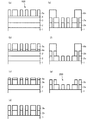
- FIG. 5 is a schematic cross-sectional view showing the manufacturing process of the phase shift mask in the embodiment of the present invention.
- the present inventors have a function of allowing a phase shift film of the mask blank to transmit KrF exposure light at a predetermined transmittance (2% or more) and transmit the same. It also has a function of producing a predetermined phase difference (150 degrees or more and 210 degrees or less) with respect to the KrF exposure light, and suppresses thermal expansion of the pattern (phase shift pattern) of the phase shift film, resulting in a phase shift pattern
- a predetermined transmittance 2% or more
- the present inventors have a function of allowing a phase shift film of the mask blank to transmit KrF exposure light at a predetermined transmittance (2% or more) and transmit the same. It also has a function of producing a predetermined phase difference (150 degrees or more and 210 degrees or less) with respect to the KrF exposure light, and suppresses thermal expansion of the pattern (phase shift pattern) of the phase shift film, resulting in a phase shift pattern
- the phase shift film having a single-layer structure is generally formed of a material having a large refractive index n and a small extinction coefficient k, because it is necessary to satisfy the required optical characteristics and film thickness.
- the back surface reflectance of the phase shift film is increased by adjusting the composition of the material forming the phase shift film to significantly increase the extinction coefficient k. If this adjustment is performed, the phase shift film cannot satisfy the condition of the transmittance within a predetermined range, so that the thickness of the phase shift film needs to be greatly reduced. However, this time, by reducing the thickness of the phase shift film, the phase shift film cannot satisfy the condition of the phase difference in the predetermined range. Since increasing the refractive index n of the material forming the phase shift film is limited, it is difficult to increase the back surface reflectance with a single-layer phase shift film.
- phase shift film was made into a laminated structure including a lower layer and an upper layer, and further study was conducted with a design concept of increasing the back surface reflectance of the entire laminated structure.
- the extinction coefficient k of the lower layer on the light-transmissive substrate side is set to be higher than the extinction coefficient k of the upper layer in order to increase the back surface reflectance more than that of the single layer structure Will also need to be increased.
- a material containing silicon has been mainly used for the phase shift film.
- the refractive index n of ArF exposure light tends to increase and the extinction coefficient k of ArF exposure light tends to decrease. Therefore, when a material having a large extinction coefficient k of ArF exposure light is selected for the lower layer, the refractive index n of ArF exposure light for the lower layer is inevitably small.
- the phase shift film has a function of causing a predetermined phase difference between the exposure light passing through the inside of the phase shift film and the exposure light passing through the air by the same distance as the thickness of the phase shift film.
- the thickness of the phase shift film is thin. Therefore, it is desired to select a material having a high refractive index n of ArF exposure light for the upper layer of the phase shift film for ArF exposure light. Considering these facts, in the case of the phase shift film for ArF exposure light, the refractive index n of the ArF exposure light of the lower layer is smaller than the refractive index n of the ArF exposure light of the upper layer, and the extinction coefficient of the ArF exposure light of the lower layer.
- phase shift film having such a structure reflects a part of ArF exposure light at the interface between the transparent substrate and the lower layer having a large extinction coefficient k of ArF exposure light.
- a part of the ArF exposure light that has entered the lower layer is further reflected at the interface between the lower layer and the upper layer where the difference in the refractive index n of the ArF exposure light is large.
- the back surface reflectance of the phase shift film with respect to ArF exposure light can be made higher than that of the single layer structure phase shift film.
- the situation of the phase shift film for KrF exposure light is different from that of the phase shift film for ArF exposure light.
- the point that the extinction coefficient k of KrF exposure light decreases as the nitrogen content increases is the same as in the case of the phase shift film for ArF exposure light.
- the refractive index n of KrF exposure light increases at the stage where the nitrogen content increases from zero to a predetermined amount, but the nitrogen content exceeds the predetermined amount. It has been found that, when the number increases, the refractive index n of KrF exposure light tends to decrease, though it increases as compared with the case where nitrogen is not contained.
- phase shift film for ArF exposure light This point is very different from the phase shift film for ArF exposure light. Also in the case of the phase shift film for KrF exposure light, it is necessary to use a material having a large extinction coefficient k of KrF exposure light for the lower layer and a material having a small extinction coefficient k of KrF exposure light for the upper layer. However, depending on the nitrogen contents of the lower layer and the upper layer, the refractive indices n of the KrF exposure light of the lower layer and the upper layer may be the same.
- the degree of design freedom is set. Is relatively narrow.
- the refractive index n of the lower KrF exposure light is larger than the refractive index n of the upper KrF exposure light, and the extinction coefficient of the lower KrF exposure light is large. It is preferable that k is larger than the extinction coefficient k of KrF exposure light in the upper layer.
- the phase shift film having such a structure reflects a part of the KrF exposure light at the interface between the transparent substrate and the lower layer having a large extinction coefficient k of the KrF exposure light.
- the phase shift film is provided with two basic functions (a predetermined transmittance for KrF exposure light and a predetermined phase difference function).
- the upper layer having a smaller extinction coefficient of KrF exposure light be thicker than the lower layer having a large extinction coefficient of KrF exposure light.
- the mask blank of the present invention is a mask blank provided with a phase shift film on a transparent substrate, and the phase shift film has a function of transmitting exposure light of a KrF excimer laser with a transmittance of 2% or more.
- FIG. 1 is a sectional view showing a configuration of a mask blank 100 according to an embodiment of the present invention.
- a mask blank 100 of the present invention shown in FIG. 1 has a structure in which a phase shift film 2, a light shielding film 3 and a hard mask film 4 are laminated in this order on a transparent substrate 1.
- the translucent substrate 1 can be made of synthetic quartz glass, quartz glass, aluminosilicate glass, soda lime glass, low thermal expansion glass (SiO 2 —TiO 2 glass, or the like).
- synthetic quartz glass has a high transmittance for KrF excimer laser light and is particularly preferable as a material for forming the transparent substrate 1 of the mask blank.
- the refractive index n of the material forming the transparent substrate 1 at the wavelength of KrF exposure light (about 248 nm) is preferably 1.44 or more and 1.58 or less, and more preferably 1.46 or more and 1.56 or less. It is more preferably 1.48 or more and 1.54 or less.
- the refractive index n when simply described as the refractive index n, it means the refractive index n with respect to the wavelength of the KrF exposure light, and when simply described as the extinction coefficient k, the extinction with respect to the wavelength of the KrF exposure light. It means a coefficient k (the same applies to subscripts n and k).
- the phase shift film 2 is required to have a transmittance of KrF exposure light of 2% or more and 40% or less.
- the transmittance for the exposure light needs to be at least 2%.
- the transmittance of the phase shift film 2 with respect to the exposure light is preferably 3% or more, and more preferably 4% or more.
- the transmittance of the phase shift film 2 with respect to the exposure light is preferably 40% or less, more preferably 35% or less, and further preferably 30% or less.
- the phase shift film 2 has a phase difference of 150 between the KrF exposure light passing therethrough and the light passing through the air by the same distance as the thickness of the phase shift film 2. It is required to be adjusted within the range of not less than 210 degrees and not more than 210 degrees.
- the phase difference in the phase shift film 2 is preferably 155 degrees or more, and more preferably 160 degrees or more.
- the phase difference in the phase shift film 2 is preferably 200 degrees or less, and more preferably 190 degrees or less. This is to reduce the influence of the increase in the phase difference due to the minute etching of the transparent substrate 1 during the dry etching when forming the pattern on the phase shift film 2.
- the phase shift film 2 has a reflectance (rear surface reflectance) on the transparent substrate 1 side (rear surface side) with respect to KrF exposure light. Is preferably 20% or more.
- the back surface reflectance of the phase shift film 2 with respect to the KrF exposure light is preferably 25% or more.
- the phase shift mask 200 manufactured from the mask blank 100 is used to perform exposure transfer to a transfer target (such as a resist film on a semiconductor wafer).
- the back surface reflectance of the phase shift film 2 with respect to the KrF exposure light is preferably 45% or less, and more preferably 40% or less.
- the phase shift film 2 has a structure in which a lower layer 21 and an upper layer 22 are stacked from the transparent substrate 1 side.
- the phase shift film 2 as a whole needs to satisfy at least the above-mentioned conditions of transmittance, phase difference, and back surface reflectance.
- the refractive index n L of the lower layer 21 and the refractive index n U of the upper layer 22 satisfy the relationship of n L >n U , and the extinction coefficient k L of the lower layer 21.
- the extinction coefficient k U of the upper layer 22 satisfies the relation of k L >k U
- the thickness d L of the lower layer 21 and the thickness d U of the upper layer 22 may satisfy the relation of d L ⁇ d U. is necessary.
- the lower layer 21 of the phase shift film 2 preferably has a refractive index n L of 2.2 or more.
- the refractive index n L of the lower layer 21 is more preferably 2.3 or more, still more preferably 2.35 or more. Further, the refractive index n L of the lower layer 21 is preferably 3.0 or less, and more preferably 2.9 or less.
- the extinction coefficient k L of the lower layer 21 is preferably 1.0 or more.
- the extinction coefficient k L of the lower layer 21 is more preferably 1.2 or more, and further preferably 1.4 or more. Further, the extinction coefficient k L of the lower layer 21 is preferably 3.8 or less, and more preferably 3.6 or less.
- the refractive index n U of the upper layer 22 is preferably 2.0 or more.
- the refractive index n U of the upper layer 22 is more preferably 2.1 or more and even more preferably 2.2 or more. Further, the refractive index n U of the upper layer 22 is preferably 2.8 or less, and more preferably 2.6 or less.
- the extinction coefficient k U of the upper layer 22 is preferably 0.01 or more, and more preferably 0.02 or more. Further, the extinction coefficient k U of the upper layer 22 is preferably 0.8 or less, and more preferably 0.6 or less.
- the difference between the refractive index n L of the lower layer 21 and the refractive index n U of the upper layer 22 is preferably 0.05 or more from the viewpoint of increasing the back surface reflectance. Further, the difference between the refractive index n L of the lower layer 21 and the refractive index n U of the upper layer 22 is preferably 1.0 or less, and more preferably 0.5 or less.
- the refractive index n of the thin film with respect to the KrF exposure light is smaller than the refractive index n of the ArF exposure light with a smaller amount of change by adjusting the composition of the thin film or the film forming method.
- the difference between the refractive index n L of the lower layer 21 and the refractive index n U of the upper layer 22 is made to be significantly larger than 1.0, the etching characteristics and durability of the lower layer 21 and the upper layer 22 may be deteriorated. There is.
- the difference between the extinction coefficient k L of the lower layer 21 and the extinction coefficient k U of the upper layer 22 is preferably 1.0 or more, and more preferably 1.2 or more. For the above reason, it is difficult to increase the difference between the refractive index n L of the lower layer 21 and the refractive index n U of the upper layer 22 so that the extinction coefficient k L of the lower layer 21 and the extinction coefficient k U of the upper layer 22 are It is desirable to increase the back surface reflectance by increasing the difference between 1.0 and 1.0, preferably 1.2.
- the difference between the extinction coefficient k L of the lower layer 21 and the extinction coefficient k U of the upper layer 22 is preferably 2.5 or less, and more preferably 2.3 or less.
- the extinction coefficient k of the thin film for KrF exposure light is smaller than the extinction coefficient k for ArF exposure light.
- the extinction coefficient k L of the lower layer 21 and the extinction coefficient k U of the upper layer 22 are a limit to increasing the extinction coefficient k L of the lower layer 21. Therefore, it becomes necessary to greatly reduce the extinction coefficient k U of the upper layer 22. In this case, it becomes necessary to significantly increase the overall film thickness of the phase shift film 2.
- the refractive index n and the extinction coefficient k of the thin film including the phase shift film 2 are not determined only by the composition of the thin film.
- the film density and crystalline state of the thin film are also factors that influence the refractive index n and the extinction coefficient k. Therefore, various conditions for forming a thin film by reactive sputtering are adjusted so that the thin film has a desired refractive index n and extinction coefficient k.
- a noble gas and a reactive gas oxygen gas, nitrogen gas, etc.
- the pressure in the film forming chamber during film formation by reactive sputtering, the electric power applied to the sputtering target, and the positional relationship such as the distance between the target and the transparent substrate 1 are various. Further, these film forming conditions are peculiar to the film forming apparatus and are appropriately adjusted so that the lower layer 21 and the upper layer 22 to be formed have desired refractive index n and extinction coefficient k.
- the thickness of the phase shift film 2 is desired to be 120 nm or less.
- the thickness d L of the lower layer 21 is preferably 40 nm or less, more preferably 35 nm or less, and 30 nm or less. And more preferable.
- the thickness d L of the lower layer 21 is preferably 3 nm or more, more preferably 5 nm or more, and further preferably 7 nm or more.
- the thickness d U of the upper layer 22 is preferably twice or more the thickness d L of the lower layer 21. It is more preferably 2.2 times or more. Further, considering that the thickness of the phase shift film 2 is 120 nm or less, the thickness d U of the upper layer 22 is preferably 15 times or less the thickness d L of the lower layer 21, and is 12 times or less. It is more preferable to have.
- the thickness d U of the upper layer 22 is preferably 110 nm or less, and more preferably 100 nm or less.
- the phase shift film 2 is preferably formed of a material containing silicon and nitrogen.
- the phase shift film 2 may be made of a material that further contains a metal element in addition to silicon and nitrogen.
- the metal element contained in the material forming the phase shift film 2 is preferably a transition metal element.
- the transition metal element includes molybdenum (Mo), tantalum (Ta), tungsten (W), titanium (Ti), chromium (Cr), hafnium (Hf), nickel (Ni), vanadium (V), zirconium.
- One or more metal elements selected from (Zr), ruthenium (Ru), rhodium (Rh), zinc (Zn), niobium (Nb) and palladium (Pd) can be mentioned.
- examples of the metal element other than the transition metal element contained in the material forming the phase shift film 2 include aluminum (Al), indium (In), tin (Sn), gallium (Ga), and the like.
- the material forming the phase shift film 2 may include elements such as carbon (C), hydrogen (H), boron (B), germanium (Ge), and antimony (Sb) in addition to the above elements. ..
- the material forming the phase shift film 2 may include an inert gas such as helium (He), argon (Ar), krypton (Kr), and xenon (Xe).
- the phase shift film 2 may be formed of a material composed of silicon and nitrogen, or a material composed of one or more elements selected from non-metal elements and semi-metal elements, and nitrogen and silicon.
- the phase shift film 2 may contain any semimetal element in addition to silicon.
- these semi-metal elements it is preferable to contain one or more elements selected from boron, germanium, antimony and tellurium because the conductivity of silicon used as a sputtering target can be expected to be increased.
- the phase shift film 2 may contain any non-metal element in addition to nitrogen.
- the non-metal element means a non-metal element in a narrow sense (nitrogen, carbon, oxygen, phosphorus, sulfur, selenium), halogen and a noble gas.
- these non-metal elements it is preferable to contain one or more elements selected from carbon, fluorine and hydrogen.
- the phase shift film 2 preferably has an oxygen content of 10 atomic% or less, more preferably 5 atomic% or less, and does not actively contain oxygen (according to X-ray photoelectron spectroscopy analysis or the like. It is more preferable that the lower limit of detection is not exceeded when composition analysis is performed.).
- the refractive index n L of the lower layer 21 and the refractive index n U of the upper layer 22 satisfy the relationship of n L >n U
- the extinction coefficient k L of the lower layer 21 and the extinction coefficient of the upper layer 22 are
- the coefficient k U needs to satisfy the relationship of k L >k U.
- the lower layer 21 of the phase shift film 2 is preferably formed of a material that does not substantially contain oxygen. This is because the degree of decrease in the extinction coefficient k L due to the increase in the oxygen content in the material is extremely large, which is not preferable to satisfy the above relationship.
- the material that does not substantially contain oxygen is a material having an oxygen content of at least 5 atomic% or less.
- the oxygen content of the material forming the lower layer 21 of the phase shift film 2 is preferably 3 atomic% or less, and more preferably the detection lower limit value or less when composition analysis by X-ray photoelectron spectroscopy or the like is performed.
- the upper layer 22 may have a surface layer having a higher oxygen content than the upper layer 22 excluding the surface layer (hereinafter, simply referred to as a surface oxide layer).
- the surface oxide layer of the upper layer 22 preferably has a thickness of 5 nm or less, and more preferably 3 nm or less.
- the refractive index n U and the extinction coefficient k U of the upper layer 22 are average values of the entire upper layer 22 including the surface oxide layer. Since the ratio of the surface oxide layer in the upper layer 22 is considerably small, the presence of the surface oxide layer has a small effect on the refractive index n U and the extinction coefficient k U of the entire upper layer 22.
- the material forming the phase shift film 2 contains nitrogen.
- the upper layer 22 preferably has a higher nitrogen content than the material forming the lower layer 21.
- the nitrogen content of the lower layer 21 is preferably 30 atomic% or less, and more preferably 25 atomic% or less.
- the nitrogen content of the upper layer 22 (the average value of the entire upper layer 22 including the surface oxide layer) is preferably more than 30 atom %, and more preferably 35 atom% or more.
- the nitrogen content of the upper layer 22 (the average value of the entire upper layer 22 including the surface oxide layer) is preferably 54 atom% or less, and more preferably 50 atom% or less.
- the lower layer 21 is preferably formed in contact with the surface of the transparent substrate 1. This is because when the lower layer 21 is in contact with the surface of the translucent substrate 1, the effect of increasing the back surface reflectance generated by the laminated structure of the lower layer 21 and the upper layer 22 of the phase shift film 2 can be obtained more.
- An etching stopper film may be provided between the translucent substrate 1 and the phase shift film 2 as long as the effect on the effect of increasing the back surface reflectance of the phase shift film 2 is small. In this case, the thickness of the etching stopper film needs to be 10 nm or less, preferably 7 nm or less, and more preferably 5 nm or less.
- the thickness of the etching stopper film needs to be 3 nm or more.
- the extinction coefficient k of the material forming the etching stopper film needs to be less than 0.1, preferably 0.05 or less, and more preferably 0.01 or less.
- the refractive index n of the material forming the etching stopper film in this case must be at least 2.4 or less, and preferably 2.1 or less.
- the refractive index n of the material forming the etching stopper film is preferably 1.5 or more.
- Ratio [%] obtained by dividing the metal content [atomic %] in the material forming the lower layer 21 and the upper layer 22 by the total metal and silicon content [atomic %] (hereinafter, this ratio is referred to as “M/[M+Si] ratio”). Is 1% or more, more preferably 2% or more, and further preferably 3% or more.
- the M/[M+Si] ratio in the material forming the lower layer 21 and the upper layer 22 is preferably 33% or less, more preferably 30% or less, and further preferably 25% or less.
- the material forming the lower layer 21 and the material forming the upper layer 22 contain a metal element, it is preferable that both contain the same metal element.
- the upper layer 22 and the lower layer 21 are patterned by dry etching using the same etching gas. Therefore, it is desirable to etch the upper layer 22 and the lower layer 21 in the same etching chamber.
- the metal elements contained in the materials forming the upper layer 22 and the lower layer 21 are the same, it is possible to reduce the environmental change in the etching chamber when the target of dry etching changes from the upper layer 22 to the lower layer 21. it can.
- the lower layer 21 and the upper layer 22 in the phase shift film 2 are formed by sputtering, but any sputtering such as DC sputtering, RF sputtering and ion beam sputtering can be applied. Considering the film forming rate, it is preferable to apply DC sputtering. When a target having low conductivity is used, it is preferable to apply RF sputtering or ion beam sputtering, but it is more preferable to apply RF sputtering in consideration of the film forming rate.
- the phase shift film 2 may be configured to have another layer on the upper layer 22.
- the other layer may be, for example, a top layer made of a material containing silicon and oxygen.
- the resistance of the phase shift film 2 to dry etching performed when removing the light shielding film 3 can be further improved.
- the uppermost layer preferably has a total content of silicon and oxygen of 80 atom% or more, more preferably 90 atom% or more, and further preferably 95 atom% or more. ..
- the thickness of the uppermost layer is preferably 10 nm or less, and more preferably 5 nm or less.
- the thickness of the uppermost layer is preferably 1 nm or more, and more preferably 2 nm or more.
- the mask blank 100 includes a light shielding film 3 on the phase shift film 2.
- a binary type transfer mask an outer peripheral region of a region where a transfer pattern is formed (transfer pattern forming region) is transmitted through the outer peripheral region when exposed and transferred to a resist film on a semiconductor wafer using an exposure device. It is required to secure an optical density (OD) of a predetermined value or more so that the resist film is not affected by the exposure light. This is also the case with the phase shift mask. In general, it is considered desirable that the OD is 3.0 or more in the outer peripheral region of the transfer mask including the phase shift mask, and at least 2.8 or more is required.
- the phase shift film 2 has a function of transmitting exposure light with a predetermined transmittance, and it is difficult to secure a predetermined optical density with the phase shift film 2 alone. Therefore, at the stage of manufacturing the mask blank 100, it is necessary to stack the light shielding film 3 on the phase shift film 2 in order to secure the insufficient optical density. With such a structure of the mask blank 100, the light-shielding film 3 in the region where the phase shift effect is used (basically the transfer pattern formation region) is removed during the manufacturing of the phase shift mask 200 (see FIG. 2). By doing so, it is possible to manufacture the phase shift mask 200 in which the optical density of the predetermined value is secured in the outer peripheral region.
- the light-shielding film 3 may have a single-layer structure or a laminated structure of two or more layers. Moreover, even if each layer of the light-shielding film 3 having a single-layer structure and the light-shielding film 3 having a laminated structure of two or more layers has the same composition in the thickness direction of the film or layers, the composition in the thickness direction of the layers is It may have an inclined structure.
- the mask blank 100 in the form shown in FIG. 1 has a structure in which the light shielding film 3 is laminated on the phase shift film 2 without interposing another film.
- the light-shielding film 3 needs to be made of a material having sufficient etching selectivity with respect to the etching gas used when forming the pattern on the phase shift film 2.
- the light shielding film 3 is preferably made of a material containing chromium.
- a material containing chromium forming the light-shielding film 3 in addition to chromium metal, a material containing one or more elements selected from oxygen, nitrogen, carbon, boron and fluorine in chromium can be mentioned.
- the material forming the light-shielding film 3 includes chromium and one or more elements selected from oxygen, nitrogen, carbon, boron and fluorine. Materials containing are preferred. Further, the chromium-containing material forming the light-shielding film 3 may contain one or more elements of molybdenum, indium and tin. By containing at least one element of molybdenum, indium, and tin, the etching rate for a mixed gas of chlorine-based gas and oxygen gas can be increased.
- the mask blank 100 of another embodiment also includes a configuration in which another film (etching stopper film) is interposed between the phase shift film 2 and the light shielding film 3.
- the etching stopper film is formed of the material containing chromium and the light shielding film 3 is formed of the material containing silicon or the material containing tantalum.
- the material containing silicon forming the light-shielding film 3 may contain a transition metal, or may contain a metal element other than the transition metal. This is because, when the light-shielding film 3 contains a transition metal, the light-shielding performance is greatly improved and the thickness of the light-shielding film 3 can be reduced as compared with the case where no transition metal is contained.
- the transition metal contained in the light shielding film 3 is molybdenum (Mo), tantalum (Ta), tungsten (W), titanium (Ti), chromium (Cr), hafnium (Hf), nickel (Ni), vanadium (V).
- metal elements other than the transition metal element contained in the light-shielding film 3 include aluminum (Al), indium (In), tin (Sn), gallium (Ga), and the like.
- the hard mask film 4 formed of a material having etching selectivity with respect to the etching gas used for etching the light shielding film 3 is further laminated on the light shielding film 3. Since the light-shielding film 3 has an essential function of ensuring a predetermined optical density, there is a limit in reducing the thickness thereof. It is sufficient for the hard mask film 4 to have a film thickness that can function as an etching mask until the dry etching for forming a pattern on the light-shielding film 3 immediately below the hard mask film 4 is completed. Not subject to the restrictions of. Therefore, the thickness of the hard mask film 4 can be made significantly smaller than the thickness of the light shielding film 3.
- the resist film made of an organic material needs to have a film thickness sufficient to function as an etching mask until the dry etching for forming a pattern on the hard mask film 4 is completed.
- the thickness can be greatly reduced.
- the thinning of the resist film is effective in improving the resist resolution and preventing the pattern collapse, and is extremely important in meeting the demand for miniaturization.
- the hard mask film 4 is preferably made of the above-mentioned material containing silicon. Since the hard mask film 4 in this case tends to have low adhesion to the resist film of an organic material, the surface of the hard mask film 4 is subjected to HMDS (Hexamethyldisilazane) treatment to improve the adhesion of the surface. It is preferable.
- the hard mask film 4 in this case is more preferably formed of SiO 2 , SiN, SiON, or the like.
- the material of the hard mask film 4 when the light-shielding film 3 is made of a material containing chromium
- a material containing tantalum can be applied in addition to the above.
- the material containing tantalum includes, in addition to tantalum metal, a material containing tantalum containing one or more elements selected from nitrogen, oxygen, boron, carbon and silicon.
- the hard mask film 4 is preferably made of the above-mentioned material containing chromium.
- a resist film of an organic material is formed in contact with the surface of the hard mask film 4.
- the phase shift mask 200 of this embodiment is characterized in that a transfer pattern (phase shift pattern) is formed on the phase shift film 2 of the mask blank 100 and a light shielding band pattern is formed on the light shielding film 3.
- a transfer pattern phase shift pattern
- a light shielding band pattern is formed on the light shielding film 3.
- the method for manufacturing the phase shift mask 200 according to the present invention uses the mask blank 100 described above, and uses a step of forming a transfer pattern on the light-shielding film 3 by dry etching and the light-shielding film 3 having the transfer pattern as a mask.
- the method is characterized by including a step of forming a transfer pattern on the phase shift film 2 by dry etching and a step of forming a light shielding band pattern on the light shielding film 3 by dry etching using the resist film 6b having the light shielding band pattern as a mask. ..
- a method of manufacturing the phase shift mask 200 of the present invention will be described according to the manufacturing process shown in FIG.
- phase shift mask 200 using the mask blank 100 in which the hard mask film 4 is laminated on the light shielding film 3 will be described. Further, a material containing chromium is applied to the light shielding film 3, and a material containing silicon is applied to the hard mask film 4.
- a resist film is formed by spin coating in contact with the hard mask film 4 in the mask blank 100.
- a first pattern which is a transfer pattern (phase shift pattern) to be formed on the phase shift film 2
- a predetermined process such as a development process is performed to perform the phase
- a first resist pattern 5a having a shift pattern was formed (see FIG. 2A).
- dry etching using a fluorine-based gas was performed using the first resist pattern 5a as a mask to form a first pattern (hard mask pattern 4a) on the hard mask film 4 (see FIG. 2B). ..
- a resist film was formed on the mask blank 100 by a spin coating method.
- a second pattern which is a pattern (light-shielding band pattern) to be formed on the light-shielding film 3
- predetermined processing such as development processing is performed to form the light-shielding pattern.
- the 2nd resist pattern 6b which has is formed (refer FIG.2(e)).
- dry etching was performed using a mixed gas of chlorine-based gas and oxygen gas to form a second pattern (light-shielding pattern 3b) on the light-shielding film 3 (FIG. 2( See f)).
- the second resist pattern 6b was removed, and predetermined processing such as cleaning was performed to obtain a phase shift mask 200 (see FIG. 2(g)).
- the chlorine-based gas used in the dry etching is not particularly limited as long as it contains Cl.
- Cl 2 , SiCl 2 , CHCl 3 , CH 2 Cl 2 , CCl 4 , BCl 3 and the like can be mentioned.
- the fluorine-based gas used in the dry etching is not particularly limited as long as it contains F.
- CHF 3 , CF 4 , C 2 F 6 , C 4 F 8 , SF 6 and the like can be mentioned.
- the fluorine-based gas not containing C has a relatively low etching rate with respect to the glass substrate, damage to the glass substrate can be further reduced.
- phase shift mask 200 of the present invention is manufactured using the mask blank 100 described above. Therefore, the phase shift film 2 (phase shift pattern 2a) on which the transfer pattern is formed has a transmittance of 2% or more for KrF exposure light, and the exposure light transmitted through the phase shift pattern 2a and the thickness of the phase shift pattern 2a. And the phase difference between the exposure light and the exposure light that has passed through the air by the same distance is within the range of 150 degrees or more and 210 degrees or less.
- the phase shift pattern 2a includes a structure in which a lower layer 21 and an upper layer 22 are sequentially stacked from the transparent substrate 1 side, the lower layer 21 has a refractive index n L at the wavelength of the exposure light, and the upper layer 22 has a refractive index at the wavelength of the exposure light.
- the phase shift mask 200 of the present invention has a back surface reflectance of the phase shift pattern 2a with respect to KrF exposure light of at least 20% or more, and thermal expansion of the phase shift pattern 2a caused by irradiation of KrF exposure light and a phase shift related to the thermal expansion. The movement of the pattern 2a can be suppressed.
- a method of manufacturing a semiconductor device of the present invention is characterized in that a pattern is exposed and transferred to a resist film on a semiconductor substrate using the phase shift mask 200 manufactured using the phase shift mask 200 or the mask blank 100 described above. I am trying. Therefore, the phase shift mask 200 is set in an exposure apparatus, and KrF exposure light is irradiated from the side of the transparent substrate 1 of the phase shift mask 200 to perform exposure transfer to a transfer target (resist film on a semiconductor wafer). Even if it is performed, the desired pattern can be transferred to the transfer target with high accuracy.
- Example 1 Manufacture of mask blanks
- the light-transmissive substrate 1 had its end face and main surface polished to a predetermined surface roughness, and then subjected to a predetermined cleaning treatment and drying treatment.
- the refractive index n S was 1.51 and the extinction coefficient k S was 0.00.
- the translucent substrate 1 on which the lower layer 21 is formed is placed in the single-wafer DC sputtering apparatus, and the upper layer 22 (MoSiN film) of the phase shift film 2 made of molybdenum, silicon, and nitrogen is placed on the lower layer 21. ) was formed.
- Mo molybdenum
- Si silicon
- He helium
- the nitrogen gas flow rate ratio of the sputtering gas used when forming the upper layer 22 is higher than the nitrogen gas flow rate ratio of the sputtering gas used when forming the lower layer 21.
- the nitrogen content of the upper layer 22 is higher than the nitrogen content of the lower layer 21.
- the phase shift film 2 in which the lower layer 21 and the upper layer 22 were laminated was formed in a thickness of 100 nm in contact with the surface of the transparent substrate 1.
- the transparent substrate 1 on which the phase shift film 2 was formed was subjected to a heat treatment for reducing the film stress of the phase shift film 2 and for forming an oxide layer on the surface layer.
- a heating furnace electric furnace
- a phase shift film 2 in which a lower layer 21 and an upper layer 22 were laminated was formed on the main surface of another light-transmissive substrate 1 under the same conditions, and heat treatment was performed to prepare the same.
- the transmittance and the phase difference of the phase shift film 2 with respect to light having a wavelength of 248 nm were measured using a phase shift amount measuring device (MPM248 manufactured by Lasertec Co., Ltd.), and the transmittance was 5.3% and the phase difference was 179.1. It was a degree (deg).
- MPM248 manufactured by Lasertec Co., Ltd.
- the phase shift film 2 was analyzed by STEM and EDX, it was confirmed that an oxide layer was formed with a thickness of about 1.7 nm from the surface of the upper layer 22 of the phase shift film 2. ..
- the lower layer 21 had a refractive index n L of 2.499 and an extinction coefficient k L of 2.587
- the upper layer 22 had The refractive index n U is 2.343
- the extinction coefficient k U is 0.315
- the difference between the refractive index n L and the refractive index n U is 1.0 or less
- the extinction coefficient k L and the extinction coefficient k are The difference in U was 2.5 or less.
- the back surface reflectance of the phase shift film 2 (reflectance on the transparent substrate 1 side) was 33%.
- the translucent substrate 1 on which the phase shift film 2 was formed was placed in a single-wafer DC sputtering apparatus, and the lowermost layer of the light shielding film 3 made of CrOCN was formed on the phase shift film 2.
- the lowermost layer of the light-shielding film 3 made of CrOCN was formed to a thickness of 30 nm on the phase shift film 2 by reactive sputtering (DC sputtering).
- the light-transmissive substrate 1 on which the phase shift film 2 and the light-shielding film 3 were laminated was placed in a single-wafer RF sputtering apparatus, and a hard mask film 4 made of silicon and oxygen was formed.
- a hard mask film 4 having a thickness of 5 nm was formed on the light shielding film 3 by RF sputtering using a silicon dioxide (SiO 2 ) target and using argon (Ar) gas as a sputtering gas.
- the mask blank 100 having a structure in which the phase shift film 2 having the two-layer structure, the light shielding film 3, and the hard mask film 4 were laminated on the transparent substrate 1 was manufactured.
- phase shift mask 200 of Example 1 was manufactured by the following procedure. First, the surface of the hard mask film 4 was subjected to HMDS treatment. Subsequently, a resist film made of a chemically amplified resist for electron beam drawing having a film thickness of 150 nm was formed in contact with the surface of the hard mask film 4 by a spin coating method. Then, a first pattern, which is a phase shift pattern to be formed on the phase shift film 2, is electron beam-drawn on the resist film, and a predetermined developing process and cleaning process are performed to obtain a first pattern having the first pattern. A resist pattern 5a of No. 1 was formed (see FIG. 2A).
- first resist pattern 5a As a mask, dry etching was performed using CF 4 gas to form a first pattern (hard mask pattern 4a) on the hard mask film 4 (see FIG. 2B). ..
- a resist film made of a chemically amplified resist for electron beam writing having a film thickness of 150 nm was formed on the light shielding pattern 3a by a spin coating method.
- a second pattern which is a pattern (light-shielding band pattern) to be formed on the light-shielding film, is exposed and drawn on the resist film, and a predetermined process such as a developing process is further performed to form a second light-shielding pattern.
- a resist pattern 6b was formed (see FIG. 2(e)).
- the manufactured halftone phase shift mask 200 of Example 1 is set on the mask stage of an exposure device that uses KrF excimer laser as exposure light, and KrF exposure light is irradiated from the transparent substrate 1 side of the phase shift mask 200.
- the pattern was exposed and transferred to the resist film on the semiconductor device.
- a predetermined process was performed on the resist film after the exposure and transfer to form a resist pattern, and the resist pattern was observed with a SEM (Scanning Electron Microscope).
- SEM Sccanning Electron Microscope
- Example 2 Manufacture of mask blanks
- the mask blank 100 of Example 2 was manufactured by the same procedure as that of Example 1 except for the phase shift film 2.
- the phase shift film 2 of Example 2 has different materials and thicknesses for forming the lower layer 21 and the upper layer 22, respectively.
- the transparent substrate 1 is installed in a single-wafer DC sputtering apparatus, and the lower layer 21 (MoSiN film) of the phase shift film 2 made of molybdenum, silicon and nitrogen is formed on the transparent substrate 1. did.
- the translucent substrate 1 on which the lower layer 21 is formed is placed in the single-wafer DC sputtering apparatus, and the upper layer 22 (MoSiN film) of the phase shift film 2 made of molybdenum, silicon, and nitrogen is placed on the lower layer 21. ) was formed.
- the nitrogen content of the upper layer 22 is higher than the nitrogen content of the lower layer 21.
- the phase shift film 2 in which the lower layer 21 and the upper layer 22 were laminated was formed in a thickness of 95 nm in contact with the surface of the transparent substrate 1.
- the heat treatment was also performed on the phase shift film 2 of Example 2 under the same treatment conditions as in Example 1.
- a phase shift film 2 of Example 2 was formed on the main surface of another transparent substrate 1 under the same conditions, and heat treatment was performed to prepare the same.
- the transmittance and the phase difference of the phase shift film 2 with respect to light having a wavelength of 248 nm were measured using a phase shift amount measuring device (MPM248 manufactured by Lasertec Co., Ltd.).
- the transmittance was 5.3% and the phase difference was 180.5. It was a degree (deg).
- the phase shift film 2 was analyzed by STEM and EDX, it was confirmed that an oxide layer was formed with a thickness of about 1.6 nm from the surface of the upper layer 22 of the phase shift film 2. ..
- Example 3 Manufacture of mask blanks
- the mask blank 100 of Example 3 was manufactured by the same procedure as that of Example 1 except for the phase shift film 2.
- the phase shift film 2 of Example 3 has different materials and thicknesses for forming the lower layer 21 and the upper layer 22, respectively.
- the transparent substrate 1 was placed in a single-wafer RF sputtering apparatus, and the lower layer 21 (SiN film) of the phase shift film 2 made of silicon and nitrogen was formed on the transparent substrate 1.
- the translucent substrate 1 on which the lower layer 21 is formed is placed in a single-wafer RF sputtering apparatus, and the upper layer 22 (SiN film) of the phase shift film 2 made of silicon and nitrogen is 69 nm on the lower layer 21.
- the upper layer 22 was formed with a thickness d U of 69 nm by (RF sputtering).
- the nitrogen gas flow rate ratio of the sputtering gas used when forming the upper layer 22 is higher than the nitrogen gas flow rate ratio of the sputtering gas used when forming the lower layer 21.
- the nitrogen content of the upper layer 22 is higher than the nitrogen content of the lower layer 21.
- the heat treatment was also performed on the phase shift film 2 of Example 3 under the same treatment conditions as in Example 1.
- a phase shift film 2 of this Example 3 was formed on the main surface of another transparent substrate 1 under the same conditions, and a heat treatment was performed to prepare it.
- the transmittance and the phase difference of the phase shift film 2 for light having a wavelength of 248 nm were measured using a phase shift measuring device (MPM248 manufactured by Lasertec Co., Ltd.), and the transmittance was 5.7% and the phase difference was 178 degrees ( deg). Further, when the phase shift film 2 was analyzed by STEM and EDX, it was confirmed that an oxide layer was formed with a thickness of about 1.3 nm from the surface of the upper layer 22 of the phase shift film 2. ..
- the lower layer 21 had a refractive index n L of 2.400 and an extinction coefficient k L of 2.040
- the upper layer 22 had The refractive index n U is 2.320
- the extinction coefficient k U is 0.040
- the difference between the refractive index n L and the refractive index n U is 1.0 or less
- the extinction coefficient k L and the extinction coefficient k are The difference in U was 2.5 or less.
- the back surface reflectance of the phase shift film 2 (reflectance on the transparent substrate 1 side) was 30%.
- the mask blank of Example 3 having a structure in which the phase shift film 2 including the lower layer 21 of SiN and the upper layer 22 of SiN, the light shielding film 3, and the hard mask film 4 are laminated on the transparent substrate 1. 100 was produced.
- phase shift mask 200 of Example 3 was produced in the same procedure as in Example 1.
- the manufactured halftone phase shift mask 200 of Example 3 is set on the mask stage of an exposure apparatus that uses KrF excimer laser as exposure light, and the phase shift mask 200 is irradiated with KrF exposure light from the transparent substrate 1 side.
- the pattern was exposed and transferred to the resist film on the semiconductor device.
- a predetermined process was performed on the resist film after the exposure and transfer to form a resist pattern, and the resist pattern was observed with a SEM (Scanning Electron Microscope).
- SEM Sccanning Electron Microscope
- Comparative Example 1 Manufacture of mask blanks
- the mask blank of Comparative Example 1 was manufactured by the same procedure as in Example 1 except for the phase shift film.
- Mo molybdenum
- Si silicon
- a phase shift film having a thickness of 92 nm was formed by DC sputtering).
- a phase shift film of Comparative Example 1 was formed under the same conditions on the main surface of another transparent substrate.
- a phase shift amount measuring device MPM248 manufactured by Lasertec Co., Ltd.
- the transmittance and the phase difference of the phase shift film with respect to light having a wavelength of 248 nm were measured, and the transmittance was 5.5% and the phase difference was 177 degrees (deg. )Met.
- the refractive index n was 2.30 and the extinction coefficient k was 0.57.
- the prepared halftone phase shift mask of Comparative Example 1 was set on the mask stage of an exposure device using KrF excimer laser as exposure light, and the semiconductor substrate was irradiated with KrF exposure light from the transparent substrate 1 side of the phase shift mask.
- the pattern was exposed and transferred to the resist film on the device.
- a predetermined process was performed on the resist film after the exposure and transfer to form a resist pattern, and the resist pattern was observed with a SEM (Scanning Electron Microscope).
- SEM Sccanning Electron Microscope
Landscapes
- Physics & Mathematics (AREA)
- General Physics & Mathematics (AREA)
- Chemical & Material Sciences (AREA)
- Chemical Kinetics & Catalysis (AREA)
- Engineering & Computer Science (AREA)
- Materials Engineering (AREA)
- Mechanical Engineering (AREA)
- Metallurgy (AREA)
- Organic Chemistry (AREA)
- Exposure And Positioning Against Photoresist Photosensitive Materials (AREA)
- Preparing Plates And Mask In Photomechanical Process (AREA)
Abstract
Description
(構成1)
透光性基板上に、位相シフト膜を備えたマスクブランクであって、
前記位相シフト膜は、KrFエキシマレーザーの露光光を2%以上の透過率で透過させる機能と、前記位相シフト膜を透過した前記露光光に対して前記位相シフト膜の厚さと同じ距離だけ空気中を通過した前記露光光との間で150度以上210度以下の位相差を生じさせる機能とを有し、
前記位相シフト膜は、前記透光性基板側から下層および上層が順に積層した構造を含み、
前記下層の前記露光光の波長における屈折率をnL、前記上層の前記露光光の波長における屈折率をnUとしたとき、nL>nUの関係を満たし、
前記下層の前記露光光の波長における消衰係数をkL、前記上層の前記露光光の波長における消衰係数をkUとしたとき、kL>kUの関係を満たし、
前記下層の厚さをdL、前記上層の厚さをdUとしたとき、dL<dUの関係を満たすことを特徴とするマスクブランク。
前記上層の屈折率nUは、2.0以上であることを特徴とする構成1記載のマスクブランク。
(構成3)
前記下層の屈折率nLは、2.2以上であることを特徴とする構成1または2に記載のマスクブランク。
前記下層の消衰係数kLは、1.0以上であることを特徴とする構成1から3のいずれかに記載のマスクブランク。
(構成5)
前記上層の厚さdUは、前記下層の厚さdLの2倍以上であることを特徴とする構成1から4のいずれかに記載のマスクブランク。
前記位相シフト膜は、ケイ素と窒素を含有する材料で形成されていることを特徴とする構成1から5のいずれかに記載のマスクブランク。
(構成7)
前記下層は、前記透光性基板の表面に接して設けられていることを特徴とする構成1から6のいずれかに記載のマスクブランク。
前記下層の厚さdLは、40nm以下であることを特徴とする構成1から7のいずれかに記載のマスクブランク。
(構成9)
前記位相シフト膜上に、遮光膜を備えることを特徴とする構成1から8のいずれかに記載のマスクブランク。
透光性基板上に、転写パターンを有する位相シフト膜を備えた位相シフトマスクであって、
前記位相シフト膜は、KrFエキシマレーザーの露光光を2%以上の透過率で透過させる機能と、前記位相シフト膜を透過した前記露光光に対して前記位相シフト膜の厚さと同じ距離だけ空気中を通過した前記露光光との間で150度以上210度以下の位相差を生じさせる機能とを有し、
前記位相シフト膜は、前記透光性基板側から下層および上層が順に積層した構造を含み、
前記下層の前記露光光の波長における屈折率をnL、前記上層の前記露光光の波長における屈折率をnUとしたとき、nL>nUの関係を満たし、
前記下層の前記露光光の波長における消衰係数をkL、前記上層の前記露光光の波長における消衰係数をkUとしたとき、kL>kUの関係を満たし、
前記下層の厚さをdL、前記上層の厚さをdUとしたとき、dL<dUの関係を満たすことを特徴とする位相シフトマスク。
(構成11)
前記上層の屈折率nUは、2.0以上であることを特徴とする構成10記載の位相シフトマスク。
前記下層の屈折率nLは、2.2以上であることを特徴とする構成10または11に記載の位相シフトマスク。
(構成13)
前記下層の消衰係数kLは、1.0以上であることを特徴とする構成10から12のいずれかに記載の位相シフトマスク。
前記上層の厚さdUは、前記下層の厚さdLの2倍以上であることを特徴とする構成10から13のいずれかに記載の位相シフトマスク。
(構成15)
前記位相シフト膜は、ケイ素と窒素を含有する材料で形成されていることを特徴とする構成10から14のいずれかに記載の位相シフトマスク。
前記下層は、前記透光性基板の表面に接して設けられていることを特徴とする構成10から15のいずれかに記載の位相シフトマスク。
(構成17)
前記下層の厚さdLは、40nm以下であることを特徴とする構成10から16のいずれかに記載の位相シフトマスク。
前記位相シフト膜上に、遮光帯を含むパターンを有する遮光膜を備えることを特徴とする構成10から17のいずれかに記載の位相シフトマスク。
(構成19)
構成9記載のマスクブランクを用いた位相シフトマスクの製造方法であって、
ドライエッチングにより前記遮光膜に転写パターンを形成する工程と、
前記転写パターンを有する遮光膜をマスクとするドライエッチングにより前記位相シフト膜に転写パターンを形成する工程と、
遮光帯を含むパターンを有するレジスト膜をマスクとするドライエッチングにより前記遮光膜に遮光帯を含むパターンを形成する工程と
を備えることを特徴とする位相シフトマスクの製造方法。
構成18記載の位相シフトマスクを用い、半導体基板上のレジスト膜に転写パターンを露光転写する工程を備えることを特徴とする半導体デバイスの製造方法。
(構成21)
構成19記載の位相シフトマスクの製造方法により製造された位相シフトマスクを用い、半導体基板上のレジスト膜に転写パターンを露光転写する工程を備えることを特徴とする半導体デバイスの製造方法。
本発明者らは、位相シフトマスクを製造するためのマスクブランクにおいて、そのマスクブランクの位相シフト膜が、KrF露光光に対して所定の透過率(2%以上)で透過する機能とその透過するKrF露光光に対して所定の位相差(150度以上210度以下)を生じさせる機能を兼ね備え、位相シフト膜のパターン(位相シフトパターン)の熱膨張を抑制し、これに起因する位相シフトパターンの移動を抑制するために必要となる構成について、鋭意研究を行った。
位相シフト膜2の下層21は、酸素を実質的に含有しない材料で形成されることが好ましい。材料中の酸素含有量を増加させることによる消衰係数kLの低下度合いが非常に大きく、上述の関係を満たすには好ましくないためである。ここで、酸素を実質的に含有しない材料とは、材料中の酸素含有量が少なくとも5原子%以下である材料である。位相シフト膜2の下層21を形成する材料の酸素含有量は、3原子%以下であると好ましく、X線光電子分光法等による組成分析を行ったときに検出下限値以下であるとより好ましい。
また、上層22は、表層にその表層を除いた部分の上層22よりも酸素含有量が多い層(以下、単に表面酸化層という。)を有してもよい。上層22の表面酸化層は、厚さが5nm以下であることが好ましく、3nm以下であるとより好ましい。なお、上記の上層22の屈折率nUおよび消衰係数kUは、表面酸化層を含む上層22全体の平均値である。上層22中の表面酸化層の比率はかなり小さいため、表面酸化層の存在が上層22全体の屈折率nUおよび消衰係数kUに与える影響は小さい。
(実施例1)
[マスクブランクの製造]
主表面の寸法が約152mm×約152mmで、厚さが約6.35mmの合成石英ガラスからなる透光性基板1を準備した。この透光性基板1は、端面及び主表面を所定の表面粗さに研磨され、その後、所定の洗浄処理および乾燥処理を施されたものであった。この透光性基板1の光学特性を測定したところ、屈折率nSが1.51、消衰係数kSが0.00であった。
次に、この実施例1のマスクブランク100を用い、以下の手順で実施例1の位相シフトマスク200を作製した。最初に、ハードマスク膜4の表面にHMDS処理を施した。続いて、スピン塗布法によって、ハードマスク膜4の表面に接して、電子線描画用化学増幅型レジストからなるレジスト膜を膜厚150nmで形成した。次に、このレジスト膜に対して、位相シフト膜2に形成すべき位相シフトパターンである第1のパターンを電子線描画し、所定の現像処理および洗浄処理を行い、第1のパターンを有する第1のレジストパターン5aを形成した(図2(a)参照)。
[マスクブランクの製造]
実施例2のマスクブランク100は、位相シフト膜2以外については、実施例1と同様の手順で製造した。この実施例2の位相シフト膜2は、下層21と上層22を形成する材料と厚さをそれぞれ変更している。具体的には、枚葉式DCスパッタ装置内に透光性基板1を設置し、透光性基板1上に、モリブデン、ケイ素および窒素からなる位相シフト膜2の下層21(MoSiN膜)を形成した。モリブデン(Mo)とケイ素(Si)との混合ターゲット(Mo:Si=9原子%:91原子%)を用い、アルゴン(Ar)および窒素(N2)の混合ガス(流量比 Ar:N2=1:1)をスパッタリングガスとする反応性スパッタリング(DCスパッタリング)により、下層21を18nmの厚さdLで形成した。
次に、この実施例2のマスクブランク100を用い、実施例1と同様の手順で、実施例2の位相シフトマスク200を作製した。
[マスクブランクの製造]
実施例3のマスクブランク100は、位相シフト膜2以外については、実施例1と同様の手順で製造した。この実施例3の位相シフト膜2は、下層21と上層22を形成する材料と厚さをそれぞれ変更している。具体的には、枚葉式RFスパッタ装置内に透光性基板1を設置し、透光性基板1上に、ケイ素および窒素からなる位相シフト膜2の下層21(SiN膜)を形成した。ケイ素(Si)ターゲットを用い、クリプトン(Kr)、窒素(N2)およびヘリウム(He)の混合ガス(流量比 Kr:N2:He=5:1:20)をスパッタリングガスとする反応性スパッタリング(RFスパッタリング)により、下層21を29nmの厚さdLで形成した。
次に、この実施例3のマスクブランク100を用い、実施例1と同様の手順で、実施例3の位相シフトマスク200を作製した。
[マスクブランクの製造]
この比較例1のマスクブランクは、位相シフト膜以外については、実施例1と同様の手順で製造した。この比較例1の位相シフト膜は、モリブデン、ケイ素および窒素からなる単層構造の膜を適用した。具体的には、枚葉式DCスパッタ装置内に透光性基板を設置し、モリブデン(Mo)とケイ素(Si)との混合焼結ターゲット(Mo:Si=21原子%:79原子%)を用い、アルゴン(Ar)、窒素(N2)、酸素(O2)およびヘリウム(He)の混合ガス流量比 Ar:N2:He=1:9:6)をスパッタリングガスとする反応性スパッタリング(DCスパッタリング)により、位相シフト膜を92nmの厚さで形成した。
次に、この比較例1のマスクブランクを用い、実施例1と同様の手順で、比較例1の位相シフトマスクを作製した。
2 位相シフト膜
21 下層
22 上層
2a 位相シフトパターン
3 遮光膜
3a,3b 遮光パターン
4 ハードマスク膜
4a ハードマスクパターン
5a 第1のレジストパターン
6b 第2のレジストパターン
100 マスクブランク
200 位相シフトマスク
Claims (21)
- 透光性基板上に、位相シフト膜を備えたマスクブランクであって、
前記位相シフト膜は、KrFエキシマレーザーの露光光を2%以上の透過率で透過させる機能と、前記位相シフト膜を透過した前記露光光に対して前記位相シフト膜の厚さと同じ距離だけ空気中を通過した前記露光光との間で150度以上210度以下の位相差を生じさせる機能とを有し、
前記位相シフト膜は、前記透光性基板側から下層および上層が順に積層した構造を含み、
前記下層の前記露光光の波長における屈折率をnL、前記上層の前記露光光の波長における屈折率をnUとしたとき、nL>nUの関係を満たし、
前記下層の前記露光光の波長における消衰係数をkL、前記上層の前記露光光の波長における消衰係数をkUとしたとき、kL>kUの関係を満たし、
前記下層の厚さをdL、前記上層の厚さをdUとしたとき、dL<dUの関係を満たすことを特徴とするマスクブランク。 - 前記上層の屈折率nUは、2.0以上であることを特徴とする請求項1記載のマスクブランク。
- 前記下層の屈折率nLは、2.2以上であることを特徴とする請求項1または2に記載のマスクブランク。
- 前記下層の消衰係数kLは、1.0以上であることを特徴とする請求項1から3のいずれかに記載のマスクブランク。
- 前記上層の厚さdUは、前記下層の厚さdLの2倍以上であることを特徴とする請求項1から4のいずれかに記載のマスクブランク。
- 前記位相シフト膜は、ケイ素と窒素を含有する材料で形成されていることを特徴とする請求項1から5のいずれかに記載のマスクブランク。
- 前記下層は、前記透光性基板の表面に接して設けられていることを特徴とする請求項1から6のいずれかに記載のマスクブランク。
- 前記下層の厚さdLは、40nm以下であることを特徴とする請求項1から7のいずれかに記載のマスクブランク。
- 前記位相シフト膜上に、遮光膜を備えることを特徴とする請求項1から8のいずれかに記載のマスクブランク。
- 透光性基板上に、転写パターンを有する位相シフト膜を備えた位相シフトマスクであって、
前記位相シフト膜は、KrFエキシマレーザーの露光光を2%以上の透過率で透過させる機能と、前記位相シフト膜を透過した前記露光光に対して前記位相シフト膜の厚さと同じ距離だけ空気中を通過した前記露光光との間で150度以上210度以下の位相差を生じさせる機能とを有し、
前記位相シフト膜は、前記透光性基板側から下層および上層が順に積層した構造を含み、
前記下層の前記露光光の波長における屈折率をnL、前記上層の前記露光光の波長における屈折率をnUとしたとき、nL>nUの関係を満たし、
前記下層の前記露光光の波長における消衰係数をkL、前記上層の前記露光光の波長における消衰係数をkUとしたとき、kL>kUの関係を満たし、
前記下層の厚さをdL、前記上層の厚さをdUとしたとき、dL<dUの関係を満たすことを特徴とする位相シフトマスク。 - 前記上層の屈折率nUは、2.0以上であることを特徴とする請求項10記載の位相シフトマスク。
- 前記下層の屈折率nLは、2.2以上であることを特徴とする請求項10または11に記載の位相シフトマスク。
- 前記下層の消衰係数nLは、1.0以上であることを特徴とする請求項10から12のいずれかに記載の位相シフトマスク。
- 前記上層の厚さdUは、前記下層の厚さdLの2倍以上であることを特徴とする請求項10から13のいずれかに記載の位相シフトマスク。
- 前記位相シフト膜は、ケイ素と窒素を含有する材料で形成されていることを特徴とする請求項10から14のいずれかに記載の位相シフトマスク。
- 前記下層は、前記透光性基板の表面に接して設けられていることを特徴とする請求項10から15のいずれかに記載の位相シフトマスク。
- 前記下層の厚さdLは、40nm以下であることを特徴とする請求項10から16のいずれかに記載の位相シフトマスク。
- 前記位相シフト膜上に、遮光帯を含むパターンを有する遮光膜を備えることを特徴とする請求項10から17のいずれかに記載の位相シフトマスク。
- 請求項9記載のマスクブランクを用いた位相シフトマスクの製造方法であって、
ドライエッチングにより前記遮光膜に転写パターンを形成する工程と、
前記転写パターンを有する遮光膜をマスクとするドライエッチングにより前記位相シフト膜に転写パターンを形成する工程と、
遮光帯を含むパターンを有するレジスト膜をマスクとするドライエッチングにより前記遮光膜に遮光帯を含むパターンを形成する工程と
を備えることを特徴とする位相シフトマスクの製造方法。 - 請求項18記載の位相シフトマスクを用い、半導体基板上のレジスト膜に転写パターンを露光転写する工程を備えることを特徴とする半導体デバイスの製造方法。
- 請求項19記載の位相シフトマスクの製造方法により製造された位相シフトマスクを用い、半導体基板上のレジスト膜に転写パターンを露光転写する工程を備えることを特徴とする半導体デバイスの製造方法。
Priority Applications (5)
| Application Number | Priority Date | Filing Date | Title |
|---|---|---|---|
| US17/428,821 US11720014B2 (en) | 2019-02-13 | 2020-02-06 | Mask blank, phase shift mask, and method of manufacturing semiconductor device |
| SG11202108439YA SG11202108439YA (en) | 2019-02-13 | 2020-02-06 | Mask blank, phase shift mask, method of manufacturing phase shift mask, and method of manufacturing semiconductor device |
| KR1020217024573A KR102782121B1 (ko) | 2019-02-13 | 2020-02-06 | 마스크 블랭크, 위상 시프트 마스크, 위상 시프트 마스크의 제조 방법 및 반도체 디바이스의 제조 방법 |
| CN202080012522.7A CN113383271B (zh) | 2019-02-13 | 2020-02-06 | 掩模坯料、相移掩模、相移掩模的制造方法以及半导体器件的制造方法 |
| JP2020572202A JP7066881B2 (ja) | 2019-02-13 | 2020-02-06 | マスクブランク、位相シフトマスク、位相シフトマスクの製造方法及び半導体デバイスの製造方法 |
Applications Claiming Priority (2)
| Application Number | Priority Date | Filing Date | Title |
|---|---|---|---|
| JP2019-023891 | 2019-02-13 | ||
| JP2019023891 | 2019-02-13 |
Publications (1)
| Publication Number | Publication Date |
|---|---|
| WO2020166475A1 true WO2020166475A1 (ja) | 2020-08-20 |
Family
ID=72045419
Family Applications (1)
| Application Number | Title | Priority Date | Filing Date |
|---|---|---|---|
| PCT/JP2020/004507 Ceased WO2020166475A1 (ja) | 2019-02-13 | 2020-02-06 | マスクブランク、位相シフトマスク、位相シフトマスクの製造方法及び半導体デバイスの製造方法 |
Country Status (7)
| Country | Link |
|---|---|
| US (1) | US11720014B2 (ja) |
| JP (1) | JP7066881B2 (ja) |
| KR (1) | KR102782121B1 (ja) |
| CN (1) | CN113383271B (ja) |
| SG (1) | SG11202108439YA (ja) |
| TW (1) | TW202036153A (ja) |
| WO (1) | WO2020166475A1 (ja) |
Families Citing this family (3)
| Publication number | Priority date | Publication date | Assignee | Title |
|---|---|---|---|---|
| JP7558861B2 (ja) * | 2021-03-23 | 2024-10-01 | Hoya株式会社 | マスクブランク、位相シフトマスク及び半導体デバイスの製造方法 |
| KR102444967B1 (ko) * | 2021-04-29 | 2022-09-16 | 에스케이씨솔믹스 주식회사 | 블랭크 마스크 및 이를 이용한 포토마스크 |
| KR102882827B1 (ko) | 2022-10-13 | 2025-11-07 | 주식회사 에스앤에스텍 | 극자외선 리소그래피용 위상반전 블랭크마스크 및 포토마스크 |
Citations (2)
| Publication number | Priority date | Publication date | Assignee | Title |
|---|---|---|---|---|
| JP2001201842A (ja) * | 1999-11-09 | 2001-07-27 | Ulvac Seimaku Kk | 位相シフトフォトマスクブランクス及び位相シフトフォトマスク並びに半導体装置の製造方法 |
| JP2003322948A (ja) * | 2002-04-26 | 2003-11-14 | Hoya Corp | ハーフトーン型位相シフトマスクブランク及びハーフトーン型位相シフトマスク |
Family Cites Families (15)
| Publication number | Priority date | Publication date | Assignee | Title |
|---|---|---|---|---|
| JPS6058757B2 (ja) | 1977-11-01 | 1985-12-21 | ライオン株式会社 | 5−イソプロピル−1−オキサスピロ〔2.4〕ヘプト−4−エン |
| JPS6058757U (ja) | 1983-09-30 | 1985-04-24 | 松下電器産業株式会社 | 浴室ユニツト |
| US5595844A (en) | 1990-11-29 | 1997-01-21 | Kabushiki Kaisha Toshiba | Method of exposing light in a method of fabricating a reticle |
| JP3345447B2 (ja) * | 1991-11-13 | 2002-11-18 | 株式会社東芝 | 露光用マスクの製造方法 |
| JP2966369B2 (ja) | 1996-03-30 | 1999-10-25 | ホーヤ株式会社 | 位相シフトマスク、及び位相シフトマスクブランク |
| US5942356A (en) | 1996-03-30 | 1999-08-24 | Hoya Corporation | Phase shift mask and phase shift mask blank |
| US7011910B2 (en) | 2002-04-26 | 2006-03-14 | Hoya Corporation | Halftone-type phase-shift mask blank, and halftone-type phase-shift mask |
| US20070076833A1 (en) | 2003-09-05 | 2007-04-05 | Hans Becker | Attenuated phase shift mask blank and photomask |
| KR102251087B1 (ko) * | 2013-08-21 | 2021-05-14 | 다이니폰 인사츠 가부시키가이샤 | 마스크 블랭크, 네거티브형 레지스트막 부착 마스크 블랭크, 위상 시프트 마스크, 및 그것을 사용하는 패턴 형성체의 제조 방법 |
| JP6430155B2 (ja) * | 2014-06-19 | 2018-11-28 | Hoya株式会社 | マスクブランク、位相シフトマスク、位相シフトマスクの製造方法および半導体デバイスの製造方法 |
| KR102261621B1 (ko) * | 2014-12-26 | 2021-06-04 | 호야 가부시키가이샤 | 마스크 블랭크, 위상 시프트 마스크, 위상 시프트 마스크의 제조 방법 및 반도체 디바이스의 제조 방법 |
| JP6058757B1 (ja) | 2015-07-15 | 2017-01-11 | Hoya株式会社 | マスクブランク、位相シフトマスク、位相シフトマスクの製造方法および半導体デバイスの製造方法 |
| JP6087401B2 (ja) * | 2015-08-14 | 2017-03-01 | Hoya株式会社 | マスクブランク、位相シフトマスクおよび半導体デバイスの製造方法 |
| TWI684822B (zh) * | 2015-09-30 | 2020-02-11 | 日商Hoya股份有限公司 | 空白遮罩、相位移轉遮罩及半導體元件之製造方法 |
| KR20180101119A (ko) * | 2017-03-04 | 2018-09-12 | 주식회사 에스앤에스텍 | 위상반전 블랭크 마스크 및 포토 마스크 |
-
2020
- 2020-02-06 SG SG11202108439YA patent/SG11202108439YA/en unknown
- 2020-02-06 KR KR1020217024573A patent/KR102782121B1/ko active Active
- 2020-02-06 CN CN202080012522.7A patent/CN113383271B/zh active Active
- 2020-02-06 US US17/428,821 patent/US11720014B2/en active Active
- 2020-02-06 JP JP2020572202A patent/JP7066881B2/ja active Active
- 2020-02-06 WO PCT/JP2020/004507 patent/WO2020166475A1/ja not_active Ceased
- 2020-02-12 TW TW109104304A patent/TW202036153A/zh unknown
Patent Citations (2)
| Publication number | Priority date | Publication date | Assignee | Title |
|---|---|---|---|---|
| JP2001201842A (ja) * | 1999-11-09 | 2001-07-27 | Ulvac Seimaku Kk | 位相シフトフォトマスクブランクス及び位相シフトフォトマスク並びに半導体装置の製造方法 |
| JP2003322948A (ja) * | 2002-04-26 | 2003-11-14 | Hoya Corp | ハーフトーン型位相シフトマスクブランク及びハーフトーン型位相シフトマスク |
Also Published As
| Publication number | Publication date |
|---|---|
| CN113383271B (zh) | 2024-01-30 |
| JP7066881B2 (ja) | 2022-05-13 |
| KR20210121067A (ko) | 2021-10-07 |
| CN113383271A (zh) | 2021-09-10 |
| JPWO2020166475A1 (ja) | 2021-09-30 |
| US20220128898A1 (en) | 2022-04-28 |
| TW202036153A (zh) | 2020-10-01 |
| US11720014B2 (en) | 2023-08-08 |
| SG11202108439YA (en) | 2021-09-29 |
| KR102782121B1 (ko) | 2025-03-18 |
Similar Documents
| Publication | Publication Date | Title |
|---|---|---|
| JP6058757B1 (ja) | マスクブランク、位相シフトマスク、位相シフトマスクの製造方法および半導体デバイスの製造方法 | |
| JP6599281B2 (ja) | マスクブランク、位相シフトマスク、位相シフトマスクの製造方法および半導体デバイスの製造方法 | |
| JP6087401B2 (ja) | マスクブランク、位相シフトマスクおよび半導体デバイスの製造方法 | |
| JP6526938B1 (ja) | マスクブランク、位相シフトマスクおよび半導体デバイスの製造方法 | |
| CN109643056B (zh) | 掩模坯料、相移掩模、相移掩模的制造方法及半导体器件的制造方法 | |
| JP6271780B2 (ja) | マスクブランク、位相シフトマスクおよび半導体デバイスの製造方法 | |
| WO2019230313A1 (ja) | マスクブランク、位相シフトマスクおよび半導体デバイスの製造方法 | |
| JP7066881B2 (ja) | マスクブランク、位相シフトマスク、位相シフトマスクの製造方法及び半導体デバイスの製造方法 | |
| WO2019230312A1 (ja) | マスクブランク、位相シフトマスクおよび半導体デバイスの製造方法 | |
| JP6321265B2 (ja) | マスクブランク、位相シフトマスク、位相シフトマスクの製造方法及び半導体デバイスの製造方法 | |
| JP6490786B2 (ja) | マスクブランク、位相シフトマスクおよび半導体デバイスの製造方法 | |
| JP6896694B2 (ja) | マスクブランク、位相シフトマスク、位相シフトマスクの製造方法および半導体デバイスの製造方法 | |
| CN114930245A (zh) | 反射型掩模坯、反射型掩模、反射型掩模的制造方法、以及反射型掩模的校正方法 | |
| EP4443234A1 (en) | Blankmask for euv lithography with absorbing film, and photomask fabricated with the same | |
| JP2022079179A (ja) | マスクブランク、位相シフトマスク、及び半導体デバイスの製造方法 |
Legal Events
| Date | Code | Title | Description |
|---|---|---|---|
| 121 | Ep: the epo has been informed by wipo that ep was designated in this application |
Ref document number: 20756451 Country of ref document: EP Kind code of ref document: A1 |
|
| ENP | Entry into the national phase |
Ref document number: 2020572202 Country of ref document: JP Kind code of ref document: A |
|
| ENP | Entry into the national phase |
Ref document number: 20217024573 Country of ref document: KR Kind code of ref document: A |
|
| NENP | Non-entry into the national phase |
Ref country code: DE |
|
| 122 | Ep: pct application non-entry in european phase |
Ref document number: 20756451 Country of ref document: EP Kind code of ref document: A1 |