WO2020162092A1 - 蓄電デバイス - Google Patents
蓄電デバイス Download PDFInfo
- Publication number
- WO2020162092A1 WO2020162092A1 PCT/JP2020/000333 JP2020000333W WO2020162092A1 WO 2020162092 A1 WO2020162092 A1 WO 2020162092A1 JP 2020000333 W JP2020000333 W JP 2020000333W WO 2020162092 A1 WO2020162092 A1 WO 2020162092A1
- Authority
- WO
- WIPO (PCT)
- Prior art keywords
- storage device
- clay
- dielectric
- electricity storage
- electrode
- Prior art date
Links
- 238000003860 storage Methods 0.000 title claims abstract description 62
- 239000004927 clay Substances 0.000 claims abstract description 48
- 229910021647 smectite Inorganic materials 0.000 claims abstract description 22
- 239000013078 crystal Substances 0.000 claims abstract description 8
- 230000005611 electricity Effects 0.000 claims description 52
- 229910000278 bentonite Inorganic materials 0.000 claims description 8
- 239000000440 bentonite Substances 0.000 claims description 8
- SVPXDRXYRYOSEX-UHFFFAOYSA-N bentoquatam Chemical compound O.O=[Si]=O.O=[Al]O[Al]=O SVPXDRXYRYOSEX-UHFFFAOYSA-N 0.000 claims description 8
- 239000011229 interlayer Substances 0.000 claims description 8
- 229910001415 sodium ion Inorganic materials 0.000 claims description 8
- 150000002500 ions Chemical class 0.000 claims description 7
- -1 trimethylstearyl ammonium ions Chemical class 0.000 claims description 7
- HBBGRARXTFLTSG-UHFFFAOYSA-N Lithium ion Chemical compound [Li+] HBBGRARXTFLTSG-UHFFFAOYSA-N 0.000 claims description 3
- 229910001416 lithium ion Inorganic materials 0.000 claims description 3
- 229910044991 metal oxide Inorganic materials 0.000 claims description 2
- 150000004706 metal oxides Chemical class 0.000 claims description 2
- 238000004519 manufacturing process Methods 0.000 description 19
- 239000002734 clay mineral Substances 0.000 description 16
- 238000000034 method Methods 0.000 description 16
- 239000010408 film Substances 0.000 description 12
- 239000006185 dispersion Substances 0.000 description 10
- 239000003989 dielectric material Substances 0.000 description 9
- 238000005259 measurement Methods 0.000 description 8
- XLYOFNOQVPJJNP-UHFFFAOYSA-N water Substances O XLYOFNOQVPJJNP-UHFFFAOYSA-N 0.000 description 8
- 239000010410 layer Substances 0.000 description 7
- 229910001369 Brass Inorganic materials 0.000 description 6
- 229910052782 aluminium Inorganic materials 0.000 description 6
- 239000010951 brass Substances 0.000 description 6
- XAGFODPZIPBFFR-UHFFFAOYSA-N aluminium Chemical compound [Al] XAGFODPZIPBFFR-UHFFFAOYSA-N 0.000 description 5
- 239000007788 liquid Substances 0.000 description 5
- 229910052751 metal Inorganic materials 0.000 description 5
- 239000002184 metal Substances 0.000 description 5
- 229920005989 resin Polymers 0.000 description 4
- 239000011347 resin Substances 0.000 description 4
- 230000004888 barrier function Effects 0.000 description 3
- 239000011230 binding agent Substances 0.000 description 3
- 239000003990 capacitor Substances 0.000 description 3
- 239000011248 coating agent Substances 0.000 description 3
- 238000000576 coating method Methods 0.000 description 3
- 238000005516 engineering process Methods 0.000 description 3
- KWLMIXQRALPRBC-UHFFFAOYSA-L hectorite Chemical compound [Li+].[OH-].[OH-].[Na+].[Mg+2].O1[Si]2([O-])O[Si]1([O-])O[Si]([O-])(O1)O[Si]1([O-])O2 KWLMIXQRALPRBC-UHFFFAOYSA-L 0.000 description 3
- 229910000271 hectorite Inorganic materials 0.000 description 3
- 230000003647 oxidation Effects 0.000 description 3
- 238000007254 oxidation reaction Methods 0.000 description 3
- 239000000843 powder Substances 0.000 description 3
- 239000010409 thin film Substances 0.000 description 3
- 229910018072 Al 2 O 3 Inorganic materials 0.000 description 2
- 229910018173 Al—Al Inorganic materials 0.000 description 2
- OKTJSMMVPCPJKN-UHFFFAOYSA-N Carbon Chemical compound [C] OKTJSMMVPCPJKN-UHFFFAOYSA-N 0.000 description 2
- JRPBQTZRNDNNOP-UHFFFAOYSA-N barium titanate Chemical compound [Ba+2].[Ba+2].[O-][Ti]([O-])([O-])[O-] JRPBQTZRNDNNOP-UHFFFAOYSA-N 0.000 description 2
- 229910002113 barium titanate Inorganic materials 0.000 description 2
- 239000003985 ceramic capacitor Substances 0.000 description 2
- 238000006243 chemical reaction Methods 0.000 description 2
- 238000010586 diagram Methods 0.000 description 2
- GUJOJGAPFQRJSV-UHFFFAOYSA-N dialuminum;dioxosilane;oxygen(2-);hydrate Chemical compound O.[O-2].[O-2].[O-2].[Al+3].[Al+3].O=[Si]=O.O=[Si]=O.O=[Si]=O.O=[Si]=O GUJOJGAPFQRJSV-UHFFFAOYSA-N 0.000 description 2
- 239000000463 material Substances 0.000 description 2
- 229910052901 montmorillonite Inorganic materials 0.000 description 2
- 238000012545 processing Methods 0.000 description 2
- 229910000275 saponite Inorganic materials 0.000 description 2
- 239000000126 substance Substances 0.000 description 2
- BQCIDUSAKPWEOX-UHFFFAOYSA-N 1,1-Difluoroethene Chemical compound FC(F)=C BQCIDUSAKPWEOX-UHFFFAOYSA-N 0.000 description 1
- 229920000178 Acrylic resin Polymers 0.000 description 1
- 239000004925 Acrylic resin Substances 0.000 description 1
- 229910000838 Al alloy Inorganic materials 0.000 description 1
- 229910001018 Cast iron Inorganic materials 0.000 description 1
- 229910017518 Cu Zn Inorganic materials 0.000 description 1
- 229910017752 Cu-Zn Inorganic materials 0.000 description 1
- 229910017943 Cu—Zn Inorganic materials 0.000 description 1
- 239000002033 PVDF binder Substances 0.000 description 1
- 239000004698 Polyethylene Substances 0.000 description 1
- 239000004743 Polypropylene Substances 0.000 description 1
- 229910000831 Steel Inorganic materials 0.000 description 1
- 238000005299 abrasion Methods 0.000 description 1
- 239000000654 additive Substances 0.000 description 1
- 230000000996 additive effect Effects 0.000 description 1
- 229910045601 alloy Inorganic materials 0.000 description 1
- 239000000956 alloy Substances 0.000 description 1
- 239000010407 anodic oxide Substances 0.000 description 1
- 229910052793 cadmium Inorganic materials 0.000 description 1
- 229910052799 carbon Inorganic materials 0.000 description 1
- 238000005341 cation exchange Methods 0.000 description 1
- 239000000919 ceramic Substances 0.000 description 1
- 238000007385 chemical modification Methods 0.000 description 1
- 238000005229 chemical vapour deposition Methods 0.000 description 1
- 229920001940 conductive polymer Polymers 0.000 description 1
- 229910052802 copper Inorganic materials 0.000 description 1
- TVZPLCNGKSPOJA-UHFFFAOYSA-N copper zinc Chemical compound [Cu].[Zn] TVZPLCNGKSPOJA-UHFFFAOYSA-N 0.000 description 1
- 238000005260 corrosion Methods 0.000 description 1
- 230000007797 corrosion Effects 0.000 description 1
- 230000007547 defect Effects 0.000 description 1
- 238000011161 development Methods 0.000 description 1
- 239000002612 dispersion medium Substances 0.000 description 1
- 238000005323 electroforming Methods 0.000 description 1
- 238000007772 electroless plating Methods 0.000 description 1
- 238000005530 etching Methods 0.000 description 1
- 230000008020 evaporation Effects 0.000 description 1
- 238000001704 evaporation Methods 0.000 description 1
- 238000009501 film coating Methods 0.000 description 1
- 229910052737 gold Inorganic materials 0.000 description 1
- 239000010439 graphite Substances 0.000 description 1
- 229910002804 graphite Inorganic materials 0.000 description 1
- 230000001771 impaired effect Effects 0.000 description 1
- 238000005470 impregnation Methods 0.000 description 1
- 238000011835 investigation Methods 0.000 description 1
- 229910052742 iron Inorganic materials 0.000 description 1
- XEEYBQQBJWHFJM-UHFFFAOYSA-N iron Substances [Fe] XEEYBQQBJWHFJM-UHFFFAOYSA-N 0.000 description 1
- 238000003475 lamination Methods 0.000 description 1
- 229910052745 lead Inorganic materials 0.000 description 1
- 229910052744 lithium Inorganic materials 0.000 description 1
- 229910052749 magnesium Inorganic materials 0.000 description 1
- 239000012528 membrane Substances 0.000 description 1
- 229910021645 metal ion Inorganic materials 0.000 description 1
- 244000005700 microbiome Species 0.000 description 1
- 229930014626 natural product Natural products 0.000 description 1
- 239000002245 particle Substances 0.000 description 1
- 239000012071 phase Substances 0.000 description 1
- 238000007747 plating Methods 0.000 description 1
- 229910052697 platinum Inorganic materials 0.000 description 1
- 238000005498 polishing Methods 0.000 description 1
- 229920003229 poly(methyl methacrylate) Polymers 0.000 description 1
- 229920000058 polyacrylate Polymers 0.000 description 1
- 229920002239 polyacrylonitrile Polymers 0.000 description 1
- 229920006350 polyacrylonitrile resin Polymers 0.000 description 1
- 229920000573 polyethylene Polymers 0.000 description 1
- 239000004926 polymethyl methacrylate Substances 0.000 description 1
- 229920005672 polyolefin resin Polymers 0.000 description 1
- 229920001155 polypropylene Polymers 0.000 description 1
- 229920001343 polytetrafluoroethylene Polymers 0.000 description 1
- 239000004810 polytetrafluoroethylene Substances 0.000 description 1
- 229920002981 polyvinylidene fluoride Polymers 0.000 description 1
- 238000002360 preparation method Methods 0.000 description 1
- 238000007670 refining Methods 0.000 description 1
- 238000007789 sealing Methods 0.000 description 1
- 229910052709 silver Inorganic materials 0.000 description 1
- 239000002689 soil Substances 0.000 description 1
- 239000002904 solvent Substances 0.000 description 1
- 239000010935 stainless steel Substances 0.000 description 1
- 229910001220 stainless steel Inorganic materials 0.000 description 1
- 239000010959 steel Substances 0.000 description 1
- 229920003048 styrene butadiene rubber Polymers 0.000 description 1
- 238000004381 surface treatment Methods 0.000 description 1
- 229920003002 synthetic resin Polymers 0.000 description 1
- 239000000057 synthetic resin Substances 0.000 description 1
- 229920002803 thermoplastic polyurethane Polymers 0.000 description 1
- 229910052719 titanium Inorganic materials 0.000 description 1
- 239000012808 vapor phase Substances 0.000 description 1
- 229910052725 zinc Inorganic materials 0.000 description 1
Images

Classifications
-
- C—CHEMISTRY; METALLURGY
- C01—INORGANIC CHEMISTRY
- C01B—NON-METALLIC ELEMENTS; COMPOUNDS THEREOF; METALLOIDS OR COMPOUNDS THEREOF NOT COVERED BY SUBCLASS C01C
- C01B33/00—Silicon; Compounds thereof
- C01B33/20—Silicates
- C01B33/36—Silicates having base-exchange properties but not having molecular sieve properties
- C01B33/38—Layered base-exchange silicates, e.g. clays, micas or alkali metal silicates of kenyaite or magadiite type
- C01B33/40—Clays
-
- H—ELECTRICITY
- H01—ELECTRIC ELEMENTS
- H01G—CAPACITORS; CAPACITORS, RECTIFIERS, DETECTORS, SWITCHING DEVICES, LIGHT-SENSITIVE OR TEMPERATURE-SENSITIVE DEVICES OF THE ELECTROLYTIC TYPE
- H01G11/00—Hybrid capacitors, i.e. capacitors having different positive and negative electrodes; Electric double-layer [EDL] capacitors; Processes for the manufacture thereof or of parts thereof
- H01G11/22—Electrodes
- H01G11/30—Electrodes characterised by their material
- H01G11/50—Electrodes characterised by their material specially adapted for lithium-ion capacitors, e.g. for lithium-doping or for intercalation
-
- H—ELECTRICITY
- H01—ELECTRIC ELEMENTS
- H01G—CAPACITORS; CAPACITORS, RECTIFIERS, DETECTORS, SWITCHING DEVICES, LIGHT-SENSITIVE OR TEMPERATURE-SENSITIVE DEVICES OF THE ELECTROLYTIC TYPE
- H01G11/00—Hybrid capacitors, i.e. capacitors having different positive and negative electrodes; Electric double-layer [EDL] capacitors; Processes for the manufacture thereof or of parts thereof
- H01G11/54—Electrolytes
- H01G11/56—Solid electrolytes, e.g. gels; Additives therein
-
- H—ELECTRICITY
- H01—ELECTRIC ELEMENTS
- H01G—CAPACITORS; CAPACITORS, RECTIFIERS, DETECTORS, SWITCHING DEVICES, LIGHT-SENSITIVE OR TEMPERATURE-SENSITIVE DEVICES OF THE ELECTROLYTIC TYPE
- H01G4/00—Fixed capacitors; Processes of their manufacture
- H01G4/002—Details
- H01G4/018—Dielectrics
- H01G4/06—Solid dielectrics
- H01G4/08—Inorganic dielectrics
- H01G4/12—Ceramic dielectrics
- H01G4/1209—Ceramic dielectrics characterised by the ceramic dielectric material
-
- H—ELECTRICITY
- H01—ELECTRIC ELEMENTS
- H01G—CAPACITORS; CAPACITORS, RECTIFIERS, DETECTORS, SWITCHING DEVICES, LIGHT-SENSITIVE OR TEMPERATURE-SENSITIVE DEVICES OF THE ELECTROLYTIC TYPE
- H01G4/00—Fixed capacitors; Processes of their manufacture
- H01G4/002—Details
- H01G4/018—Dielectrics
- H01G4/06—Solid dielectrics
- H01G4/08—Inorganic dielectrics
- H01G4/12—Ceramic dielectrics
- H01G4/1272—Semiconductive ceramic capacitors
-
- H—ELECTRICITY
- H01—ELECTRIC ELEMENTS
- H01G—CAPACITORS; CAPACITORS, RECTIFIERS, DETECTORS, SWITCHING DEVICES, LIGHT-SENSITIVE OR TEMPERATURE-SENSITIVE DEVICES OF THE ELECTROLYTIC TYPE
- H01G4/00—Fixed capacitors; Processes of their manufacture
- H01G4/002—Details
- H01G4/018—Dielectrics
- H01G4/06—Solid dielectrics
- H01G4/08—Inorganic dielectrics
- H01G4/12—Ceramic dielectrics
- H01G4/129—Ceramic dielectrics containing a glassy phase, e.g. glass ceramic
-
- H—ELECTRICITY
- H01—ELECTRIC ELEMENTS
- H01G—CAPACITORS; CAPACITORS, RECTIFIERS, DETECTORS, SWITCHING DEVICES, LIGHT-SENSITIVE OR TEMPERATURE-SENSITIVE DEVICES OF THE ELECTROLYTIC TYPE
- H01G4/00—Fixed capacitors; Processes of their manufacture
- H01G4/30—Stacked capacitors
-
- C—CHEMISTRY; METALLURGY
- C01—INORGANIC CHEMISTRY
- C01P—INDEXING SCHEME RELATING TO STRUCTURAL AND PHYSICAL ASPECTS OF SOLID INORGANIC COMPOUNDS
- C01P2004/00—Particle morphology
- C01P2004/20—Particle morphology extending in two dimensions, e.g. plate-like
- C01P2004/24—Nanoplates, i.e. plate-like particles with a thickness from 1-100 nanometer
-
- H—ELECTRICITY
- H01—ELECTRIC ELEMENTS
- H01G—CAPACITORS; CAPACITORS, RECTIFIERS, DETECTORS, SWITCHING DEVICES, LIGHT-SENSITIVE OR TEMPERATURE-SENSITIVE DEVICES OF THE ELECTROLYTIC TYPE
- H01G11/00—Hybrid capacitors, i.e. capacitors having different positive and negative electrodes; Electric double-layer [EDL] capacitors; Processes for the manufacture thereof or of parts thereof
- H01G11/10—Multiple hybrid or EDL capacitors, e.g. arrays or modules
- H01G11/12—Stacked hybrid or EDL capacitors
-
- H—ELECTRICITY
- H01—ELECTRIC ELEMENTS
- H01G—CAPACITORS; CAPACITORS, RECTIFIERS, DETECTORS, SWITCHING DEVICES, LIGHT-SENSITIVE OR TEMPERATURE-SENSITIVE DEVICES OF THE ELECTROLYTIC TYPE
- H01G4/00—Fixed capacitors; Processes of their manufacture
- H01G4/002—Details
- H01G4/005—Electrodes
- H01G4/008—Selection of materials
-
- H—ELECTRICITY
- H01—ELECTRIC ELEMENTS
- H01G—CAPACITORS; CAPACITORS, RECTIFIERS, DETECTORS, SWITCHING DEVICES, LIGHT-SENSITIVE OR TEMPERATURE-SENSITIVE DEVICES OF THE ELECTROLYTIC TYPE
- H01G4/00—Fixed capacitors; Processes of their manufacture
- H01G4/002—Details
- H01G4/018—Dielectrics
- H01G4/06—Solid dielectrics
- H01G4/08—Inorganic dielectrics
-
- H—ELECTRICITY
- H01—ELECTRIC ELEMENTS
- H01G—CAPACITORS; CAPACITORS, RECTIFIERS, DETECTORS, SWITCHING DEVICES, LIGHT-SENSITIVE OR TEMPERATURE-SENSITIVE DEVICES OF THE ELECTROLYTIC TYPE
- H01G4/00—Fixed capacitors; Processes of their manufacture
- H01G4/30—Stacked capacitors
- H01G4/306—Stacked capacitors made by thin film techniques
-
- H—ELECTRICITY
- H01—ELECTRIC ELEMENTS
- H01G—CAPACITORS; CAPACITORS, RECTIFIERS, DETECTORS, SWITCHING DEVICES, LIGHT-SENSITIVE OR TEMPERATURE-SENSITIVE DEVICES OF THE ELECTROLYTIC TYPE
- H01G4/00—Fixed capacitors; Processes of their manufacture
- H01G4/33—Thin- or thick-film capacitors
-
- H—ELECTRICITY
- H01—ELECTRIC ELEMENTS
- H01M—PROCESSES OR MEANS, e.g. BATTERIES, FOR THE DIRECT CONVERSION OF CHEMICAL ENERGY INTO ELECTRICAL ENERGY
- H01M50/00—Constructional details or processes of manufacture of the non-active parts of electrochemical cells other than fuel cells, e.g. hybrid cells
- H01M50/40—Separators; Membranes; Diaphragms; Spacing elements inside cells
- H01M50/409—Separators, membranes or diaphragms characterised by the material
-
- Y—GENERAL TAGGING OF NEW TECHNOLOGICAL DEVELOPMENTS; GENERAL TAGGING OF CROSS-SECTIONAL TECHNOLOGIES SPANNING OVER SEVERAL SECTIONS OF THE IPC; TECHNICAL SUBJECTS COVERED BY FORMER USPC CROSS-REFERENCE ART COLLECTIONS [XRACs] AND DIGESTS
- Y02—TECHNOLOGIES OR APPLICATIONS FOR MITIGATION OR ADAPTATION AGAINST CLIMATE CHANGE
- Y02E—REDUCTION OF GREENHOUSE GAS [GHG] EMISSIONS, RELATED TO ENERGY GENERATION, TRANSMISSION OR DISTRIBUTION
- Y02E60/00—Enabling technologies; Technologies with a potential or indirect contribution to GHG emissions mitigation
- Y02E60/10—Energy storage using batteries
Definitions
- the present invention relates to an electricity storage device using a clay mineral as a dielectric, and more particularly to an electricity storage device in which a thin film made of clay mineral is interposed as a dielectric between electrodes.
- capacitors for digital equipment One of the concrete examples of electricity storage devices is capacitors for digital equipment. Although the required characteristics of capacitors for digital devices vary depending on the application and purpose, in recent years monolithic ceramic capacitors with excellent frequency characteristics and high durability have become the mainstream. The value of the dielectric material that constitutes this type of monolithic ceramic capacitor is increasing due to technological advances due to miniaturization and high durability. However, such miniaturization technology requires high processing technology in terms of cost. Therefore, there is a demand for the development of new materials that can be processed in the nano region at low cost.
- the dielectric material of the power storage body which is widely used at present, is subjected to fine processing in nano units for the purpose of increasing the capacity.
- conventional microfabricated capacitors in nanometer units are not yet satisfactory.
- An object of the present invention is to provide an electricity storage device using a high-capacity, inexpensive microfabricated dielectric and a method for manufacturing the same.
- ⁇ 2> The electricity storage device according to ⁇ 1>, wherein a metal oxide film is formed on a surface of the current collector having electric conductivity, which is connected to both or one of the clay films.
- ⁇ 3> The electricity storage device according to ⁇ 1> and ⁇ 2>, wherein the plate-shaped crystal structure smectite-based clay film has bentonite or smectite interlayer ions selected from sodium ions, lithium ions, and trimethylstearyl ammonium ions.
- ⁇ 4> The electricity storage device according to any one of ⁇ 1> to ⁇ 3>, which has a separator between the upper and lower electrodes.
- the electrode of the electricity storage device of the present invention has electrical conductivity that allows ohmic contact with the lead.
- the electricity storage device of the present invention has, as a dielectric, an ultrafine layered structure in which repeating units are layered up to a film thickness of about 1 nm, which is peculiar to smectite-based clay, usually from a minimum thickness of 1 nm to a maximum thickness. To do.
- the number of stacked layers (density) obtained by microfabrication of conventional dielectrics is several hundred times larger, and it is possible to manufacture an electronic device that enables smaller size and larger capacity than existing dielectrics.
- the bentonite used is one that uses naturally occurring smectite or its synthetic product or an interlayer ion-substituted product as a member, has excellent safety, and is easily processed at a relatively low cost from the viewpoint of preparation of a dielectric material and an electricity storage device. , Can be provided.
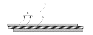
- FIG. 1 is a sectional view schematically showing a preferred embodiment of an electricity storage device according to the present invention.
- FIG. 2 is a configuration diagram schematically showing an example of measurement of relative permittivity by an electricity storage device.
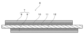
- FIG. 3 is a schematic diagram of an electricity storage device using a separator.
- the electricity storage device 1 has an upper electrode 2, a lower electrode 4, and a clay dielectric 3 between them.
- the clay dielectric 3 is the above-mentioned silicate compound or smectite clay mineral having a plate crystal structure. Smectite clay minerals include montmorillonite, hectorite, stevensite, and saponite.
- a metal current collector is used for the upper electrode 2 and the lower electrode 4 in which a thin film or powdery clay mineral is sandwiched.
- the upper electrode 2 and the lower electrode 4 may be in contact with the clay dielectric 3.
- the thickness of the dielectric is preferably 0.01 to 1 mm, but is not limited to this.
- This electricity storage device stores electricity due to the fine structure of clay.
- the above electricity storage device 1 is preferably sealed with a waterproof and gas barrier material in order to control the water content of the clay dielectric 3.
- a method of sealing using a metal case, or a method of using a lamination method to prevent evaporation of water by covering the film may be used.
- the film used at this time preferably has excellent water resistance, water vapor barrier properties, and gas barrier properties.
- the water content of the clay dielectric 3 is preferably 1 to 20% by mass, more preferably 5 to 15% by mass.
- the clay mineral at least one kind of clay selected from natural or synthetic clay is used. Such clay may be unmodified or modified, but at least one selected from smectite clays such as bentonite and hectorite is preferable. Among these, bentonite is an inorganic clay that is naturally produced and therefore has excellent safety. In addition, it is stable for a long period of time without being decomposed by microorganisms in the soil, and the price is low. Therefore, it is a particularly preferable clay mineral. As the clay mineral, one type of clay selected from bentonite and smectite can be used alone, or two types of clay can be used. The interlayer ions of bentonite and smectite are not particularly limited.
- the plate-shaped crystal structure smectite refers to, for example, a plate-shaped clay crystal having a thickness of about 1 nm and an aspect ratio of width/thickness of preferably 20 to 2000, more preferably about 30 to 300.
- Aspect ratios of typical smectite products are shown in Table 1, but the present invention is not limited thereto.
- the upper electrode 2 or the lower electrode coated with the same clay dispersion liquid again is applied as a dispersion liquid on the surfaces of the upper electrode 2 and the lower electrode 4 and naturally dried (usually water content 10% by mass) It is desirable to apply the dispersion liquid to the electrode 4 again, attach the dispersion liquid, and naturally dry it.
- a clay mineral When applying the clay mineral to the upper electrode 2 or the lower electrode 4, it is desirable to disperse the clay mineral in a solvent such as water before applying.
- a solvent such as water
- the dispersion medium one that can be dissolved and dispersed depending on the characteristics of clay can be used. It is also possible to form a layer of clay mineral between the upper electrode 2 and the lower electrode 4 in a powder state, but it is necessary to take measures so as to prevent scattering, control the coating thickness, and prevent defects.
- a clay mineral may be fixed between the electrodes by using a binder.
- the binder include styrene-butadiene rubber type, acrylic polymer type, polyvinylidene fluoride type and polytetrafluoroethylene type.
- various additive components can be optionally added to the clay dielectric as long as the object of the present invention is not impaired.
- the upper electrode 2 or the lower electrode 4 is made of, for example, a metal such as Pt, Au, Ti, Ag, Cu, Pb, Fe, Cd, Al, Zn, Mg or Li, and stainless steel, brass (Cu-Zn), cast iron, It is preferable to use steel, an alloy such as an aluminum alloy, or a current collector such as graphite or a conductive polymer.
- the electrodes 2, 4, and 7 may be functionalized by surface-treating any of them.
- Surface treatment methods include metal thin film coating, electroless plating, vapor phase plating (CVD method), anodic etching method, anodic oxidation chemical conversion, electrolytic polishing, chemical modification, electroforming, carbon coating, and carbide treatment. and so on.
- the anodic oxide coating of aluminum is a preferable electrode because it has excellent corrosion resistance and abrasion resistance.
- a separator may be used between the upper and lower electrodes to prevent a short circuit.
- An electricity storage device 6 using the separator 11 is shown in FIG.
- the separator 11 isolates the dielectrics 10 and 12 between the upper electrode 8 and the lower electrode 9, prevents contact between upper and lower electrodes and short circuit of current, and allows metal ions and electrons to pass through.
- the type of the separator 11 is not particularly limited, and may be made of, for example, an olefin resin, a PDF resin, a PAN resin, a PMMA resin, or the like.
- the separator 11 is impregnated with a dispersion liquid of clay serving as a dielectric and is naturally dried.
- the clay aqueous dispersion is a clay mineral, Kunipia F (trade name, manufactured by Kunimine Industry Co., Ltd.) (Example 1), Smecton ST (trade name, manufactured by Kunimine Industry Co., Ltd.) (Example 2), Smecton SA (trade name, Kunimine Co., Ltd.) Kogyo Co., Ltd. (Example 3) and Smecton SWN (trade name, manufactured by Kunimine Industry Co., Ltd.) (Example 4) were used.
- Kunipia F is a clay mineral obtained by refining bentonite, which is a natural product whose main component is montmorillonite (Na ions are intercalated between layers).
- Smecton ST is a synthetic clay containing stevensite as a main component (Na ion is intercalated between layers).
- Smecton SA is a synthetic clay whose main component is saponite (Na ions are intercalated between layers).
- Smecton SWN is a synthetic clay whose main component is hectorite (Na ions are intercalated between layers).
- Table 2 shows the cation exchange capacity CEC [meq/100 g] of the clay used in each example.
- Table 3 shows the results of measuring the relative dielectric constants of Examples 1 to 4 at 100 Hz and 10 kHz.
- Examples 1 to 4 obtained high relative permittivity in the electricity storage device using the smecton clay mineral as the dielectric. This shows that an inexpensive electricity storage device with a high dielectric constant can be manufactured. An electricity storage device using smecton SWN can obtain the highest relative permittivity and is most preferable as an electricity storage device.
- Examples 5-8 ⁇ Measurement of relative permittivity of electricity storage device with different collector>
- the current collector metal was changed to aluminum or brass and Kunipia F or smecton ST was used as the dielectric in the production of the above electricity storage device.
- Smecton ST was used for the clay dielectric 3
- brass was used for the electrode in the method for producing the electricity storage device.
- Example 9 SUS was used as the electrode 5 and Kunipia RC-G (manufactured by Kunimine Industries Co., Ltd.) was used as the dielectric in the method for manufacturing the electricity storage device.
- Kunipia RC-G is a smectite clay in which interlayer ions of Kunipia F are replaced with lithium ions (CEC40 [meq/100 g]).
- SUS was used as a current collector and Kunibis 110 (manufactured by Kunimine Industries Co., Ltd.) was used as a dielectric in the method for producing the electricity storage device.
- Kunibis 110 is an organically modified smectite clay in which interlayer ions of Kunipia F are replaced with sodium ions by trimethylstearyl ammonium ions.
- Table 6 shows the results of measuring the relative permittivity of Examples 9 and 10 at 100 Hz and 10 kHz.
- Examples 11 and 12 As shown in FIG. 3, a clay dispersion was applied onto the upper electrode 8 and the lower electrode 9 to form an upper dielectric 10 and a lower dielectric 12. The clay-impregnated separator 11 impregnated with the clay dispersion was sandwiched between the upper dielectric 10 and the lower dielectric 12 to form the electricity storage device 6.
- Kunipia F was used as the dielectric
- SUS430 was used as the electrode in the method of manufacturing the electricity storage device 6 described above.
- Example 12 uses Smecton ST as a dielectric and SUS430 as an electrode in the method of manufacturing the electricity storage device 6 described above.
- Example 11 and Example 12 were measured.
- Table 7 shows the measurement results of the relative permittivity of Examples 11 and 12.
- Example 13 and Example 14 were measured.
- Table 8 shows the measurement results of the relative dielectric constants of Example 13 and Example 14.
Landscapes
- Engineering & Computer Science (AREA)
- Power Engineering (AREA)
- Chemical & Material Sciences (AREA)
- Microelectronics & Electronic Packaging (AREA)
- Manufacturing & Machinery (AREA)
- Ceramic Engineering (AREA)
- Inorganic Chemistry (AREA)
- Organic Chemistry (AREA)
- Materials Engineering (AREA)
- Electrochemistry (AREA)
- Chemical Kinetics & Catalysis (AREA)
- Dispersion Chemistry (AREA)
- General Chemical & Material Sciences (AREA)
- Electric Double-Layer Capacitors Or The Like (AREA)
- Silicates, Zeolites, And Molecular Sieves (AREA)
- Fixed Capacitors And Capacitor Manufacturing Machines (AREA)
Abstract
電極を2極有し、この電極間に板状結晶構造スメクタイト系粘土膜を有する蓄電デバイス。
Description
本発明は、粘土鉱物を誘電体として使用した蓄電デバイスに関し、さらに詳しくは電極間に粘土鉱物からなる薄膜等を誘電体として介在させた蓄電デバイスに関する。
蓄電デバイスの具体例の一つにデジタル機器用コンデンサがある。デジタル機器用コンデンサは用途・目的によって要求特性は異なるが、近年では周波数特性に優れ、耐久性も高い積層セラミックコンデンサが主流となっている。この種の積層セラミックコンデンサを構成する誘電体は、微細化・高耐久化による技術進化によって価値が高められている。しかし、こうした微細化技術は加工技術がコスト的にも高くなる。そのため、安価にナノ領域での加工を実現できる新素材の開発が求められている。
現在広く使用されている蓄電体の誘電体は、高容量化を目指してナノ単位での微細加工がなされている。しかし、高い誘電率を有するが安価であるという誘電体およびその製造方法を提供するという観点から従来のナノメーター単位での微細加工コンデンサ等はまだ満足できるものとはいえない。
本発明は高容量で、廉価な微細加工誘電体を用いた蓄電デバイス及びその製造方法を提供することを課題とする。
本発明は高容量で、廉価な微細加工誘電体を用いた蓄電デバイス及びその製造方法を提供することを課題とする。
本発明らは種々検討を重ねた結果、スメクタイト系粘土に見られる特有の厚さ1nm程度の繰り返し単位が積層した超微細積層構造を誘電体とすると、比誘電率が高い値を示し、そのため従来の誘電体の微細加工による積層枚数(密度)が数百倍となり、既存の誘電体に比べて小型大容量を可能とする電子デバイスとなり得ることを見い出し、この知見に基づき、研究を重ね、本発明をなすにいたった。
本発明の上記の課題は以下の手段により解決された。
<1>
電極を2極有し、この電極間に板状結晶構造スメクタイト系粘土膜を有する蓄電デバイス。
<2>
電気伝導性を有する集電体の両方あるいは片方の粘土膜に接続する面に金属酸化被膜を形成することを特徴とする<1>記載の蓄電デバイス。
<3>
板状結晶構造スメクタイト系粘土膜がベントナイトまたはスメクタイトの層間イオンがナトリウムイオン、リチウムイオン、トリメチルステアリルアンモニウムイオンから選ばれたことを特徴とする<1>および<2>記載の蓄電デバイス。
<4>
上下電極間にセパレータを有する<1>~<3>のいずれか1に記載の蓄電デバイス。
本発明の蓄電デバイスの電極はリードとオーミックコンタクト可能な電気伝導性を有する。
本発明の蓄電デバイスは、スメクタイト系粘土に見られる特有の厚さ1nm程度、通常は最小1nm~最大で形成される膜厚に至るまでの、繰り返し単位が積層した超微細積層構造を誘電体とする。従来の誘電体の微細加工による積層枚数(密度)が数百倍となり、既存の誘電体に比べて小型大容量を可能とする電子デバイスを製造できる。さらに、用いるベントナイトは天然に産出するスメクタイト又はその合成品若しくは層間イオン置換体を部材として用いるものであり、安全性に優れ、誘電体、さらに蓄電デバイスの調製の観点から容易に比較的廉価に加工、提供することが可能となる。
本発明の上記および他の特徴および利点は、適宜添付の図面を参照して、下記の記載からより明らかになるであろう。
本発明の上記および他の特徴および利点は、適宜添付の図面を参照して、下記の記載からより明らかになるであろう。
次に本発明の好ましい一実施形態を、図1~3を参照して説明する。
図1に示すように、蓄電デバイス1は、上部電極2と下部電極4とその間の粘土誘電体3とを有している。粘土誘電体3は板状結晶構造をなしている上述のケイ酸塩化合物またはスメクタイト系粘土鉱物をいう。スメクタイト系粘土鉱物には、モンモリロナイト、ヘクトライト、スチブンサイト、サポナイトが含まれる。薄膜もしくは粉末の粘土鉱物を挟み込んだ上部電極2および下部電極4には金属集電体が用いられる。上部電極2と下部電極4とは粘土誘電体3と接触していれば良い。
誘電体の厚さは0.01~1mmが好ましいが、これに制限されるものではない。
この蓄電デバイスは、粘土の微細構造により蓄電する。
図1に示すように、蓄電デバイス1は、上部電極2と下部電極4とその間の粘土誘電体3とを有している。粘土誘電体3は板状結晶構造をなしている上述のケイ酸塩化合物またはスメクタイト系粘土鉱物をいう。スメクタイト系粘土鉱物には、モンモリロナイト、ヘクトライト、スチブンサイト、サポナイトが含まれる。薄膜もしくは粉末の粘土鉱物を挟み込んだ上部電極2および下部電極4には金属集電体が用いられる。上部電極2と下部電極4とは粘土誘電体3と接触していれば良い。
誘電体の厚さは0.01~1mmが好ましいが、これに制限されるものではない。
この蓄電デバイスは、粘土の微細構造により蓄電する。
上記の蓄電デバイス1は、粘土誘電体3の含水率を制御するために、防水性、ガスバリア材料で密閉することが好ましい。例えば、金属ケースを用いて密閉する方法や、ラミネーション法を用いて、フィルムの外装により水分の蒸発を防ぐ方法を用いてもよい。このとき用いられるフィルムは、耐水性、水蒸気バリア性、ガスバリア性に優れていることが好ましい。粘土誘電体3の含水率は、好ましくは1~20質量%、より好ましくは5~15質量%である。
上記の粘土鉱物は、天然もしくは合成の粘土から選ばれた少なくとも1種類の粘土が用いられる。このような粘土としては、未変性のものでも変性したものでもよいが、ベントナイトおよびヘクトライト等スメクタイト系粘土から選ばれた少なくとも1種が好ましい。このうち、ベントナイトは天然に産出する無機系の粘土であるため安全性に優れている。また土中の微生物によって分解されることがなく長期的に安定であり、さらに低価格である。このため、特に好ましい粘土鉱物である。上記の粘土鉱物は、ベントナイトおよびスメクタイトから選ばれた1種の粘土を単独で用いることも、または2種の粘土を用いることもできる。ベントナイトおよびスメクタイトの層間イオンは特に限定はない。
本発明において板状結晶構造スメクタイトとは、例えば厚さ1nm程度で幅/厚さのアスペクト比が好ましくは20~2000、より好ましくは約30~300の平板状の粘土結晶をいう。代表的なスメクタイト系製品(クニミネ工業社製)のアスペクト比を<表1>に示したが、本発明はこれに限定されるものではない。
本発明において板状結晶構造スメクタイトとは、例えば厚さ1nm程度で幅/厚さのアスペクト比が好ましくは20~2000、より好ましくは約30~300の平板状の粘土結晶をいう。代表的なスメクタイト系製品(クニミネ工業社製)のアスペクト比を<表1>に示したが、本発明はこれに限定されるものではない。

上記粘土鉱物を配するには、上部電極2及び下部電極4の表面に分散液として塗布し自然乾燥させ(通常含水率10質量%)、再び同様の粘土分散液を塗布した上部電極2または下部電極4に再び分散液を塗布し貼り合わせて自然乾燥させることが望ましい。
粘土鉱物を上部電極2または下部電極4に塗布する際には水などの溶媒に粘土鉱物を分散してから塗工することが望ましい。分散媒は、粘土の特性によって溶解・分散可能なものを使用することができる。粉末状態で上部電極2と下部電極4との間に粘土鉱物の層を形成することも可能であるが、飛散対策や塗工厚の制御、欠損部が発生しないように留意する必要がある。短絡防止のために、バインダーを使用し粘土鉱物を電極間に固定させてもよい。バインダーにはスチレン-ブタジエンゴム系、アクリルポリマー系、ポリフッ化ビニリデン系、ポリテトラフルオロエチレン系などが挙げられる。
また、本発明の目的を損なわない範囲で、必要に応じ、粘土誘電体に種々の添加成分を任意成分として配合することができる。
また、本発明の目的を損なわない範囲で、必要に応じ、粘土誘電体に種々の添加成分を任意成分として配合することができる。
上部電極2または下部電極4は例えば、Pt、Au、Ti、Ag、Cu、Pb、Fe、Cd、Al、Zn、Mg、Liなどの金属および、ステンレス鋼、真鍮(Cu-Zn)、鋳鉄、鋼、アルミニウム合金などの合金、または、グラファイト、導電性高分子などの集電体で構成するのが好ましい。
電極2、4、7は、いずれかに表面処理を施し、機能化した電極としてもよい。表面処理法としては、金属薄膜によるコーティングによるめっき、無電解めっきや、気相めっき(CVD法)、アノード処理によるエッチング法やアノード酸化化成、電解研磨、化学修飾や電鋳、炭素コーティング、カーバイド処理などがある。特にアルミニウムのアノード酸化被膜は耐食性、耐摩耗性にも優れており好ましい電極である。
短絡防止のために、上下電極間にセパレータを使用することができる。セパレータ11を使用した蓄電デバイス6を図3に示した。
セパレータ11は、上部電極8と下部電極9間で誘電体10、12を隔離し、上下電極の接触と電流の短絡を防止しつつ、金属イオンや電子を通過させるものである。このセパレータ11の種類は特に制限がなく、例えば、オレフィン系樹脂、PDF系樹脂、PAN系樹脂、PMMA系樹脂などからなるものがある。具体的には、ポリアクリロニトリル樹脂、フッ化ビニリデン樹脂、アクリル樹脂及びウレタン系樹脂、ポリエチレンやポリプロピレンなどよりなる合成樹脂性の多孔質膜、またはセラミック製の多孔質膜により構成されているものや、これらの2種以上の多孔質膜を積層した構成でもよい。
セパレータ11は、上部電極8と下部電極9間で誘電体10、12を隔離し、上下電極の接触と電流の短絡を防止しつつ、金属イオンや電子を通過させるものである。このセパレータ11の種類は特に制限がなく、例えば、オレフィン系樹脂、PDF系樹脂、PAN系樹脂、PMMA系樹脂などからなるものがある。具体的には、ポリアクリロニトリル樹脂、フッ化ビニリデン樹脂、アクリル樹脂及びウレタン系樹脂、ポリエチレンやポリプロピレンなどよりなる合成樹脂性の多孔質膜、またはセラミック製の多孔質膜により構成されているものや、これらの2種以上の多孔質膜を積層した構成でもよい。
セパレータ11には誘電体となる粘土の分散液が含浸され自然乾燥されていることが好ましい。
次に、本発明を下記の実施例に基づいて更に詳細に説明する。本発明はこれらの実施例により何ら限定されるものではない。
実施例1~4
図1に示したように、上部電極2厚さ0.1mm×面積S(mm2)および下部電極IV厚さ0.1mm×面積S+2(mm2)の上に、下記粘土の水分散液を塗工して自然乾燥させた(塗布粘土の含水率10質量%)。この上部電極2と下部電極4とへさらに上記と同様の粘土水分散液をバインダーとして塗布し空隙なく挟み込んだものを同様に自然乾燥させ粘土誘電体3(厚さd=0.07mm)とし、蓄電デバイス1を形成した。電極2、4からなる集電体5としてSUS430を使用した。電極2、4の厚さはそれぞれ0.1mmである。
粘土水分散液は、粘土鉱物のクニピアF(商品名、クニミネ工業社製)(実施例1)、スメクトンST(商品名、クニミネ工業社製)(実施例2)、スメクトンSA(商品名、クニミネ工業社製)(実施例3)、スメクトンSWN(商品名、クニミネ工業社製)(実施例4)を用いた。
クニピアFはモンモリロナイトを主成分とする天然物であるベントナイトを精製した粘土鉱物である(層間にNaイオンをインターカレート)。スメクトンSTは、スチブンサイトを主成分とした合成粘土である(層間にNaイオンをインターカレート)。スメクトンSAはサポナイトを主成分とした合成粘土である(層間にNaイオンをインターカレート)。スメクトンSWNはヘクトライトを主成分とした合成粘土である(層間にNaイオンをインターカレート)。各々の実施例で使用した粘土の陽イオン交換容量CEC[meq/100g]を表2に示す。

<蓄電デバイス1を用いた比誘電率の計測>
図2に示したように、蓄電デバイスのインピーダンスZ[Ω]及び位相角θをLCRメータ:HIOKI-3522-50 LCR Hi TESTER(日置電機株式会社製)を用いてlevel 100mVで測定し、比誘電率を計測した。
図2に示したように、蓄電デバイスのインピーダンスZ[Ω]及び位相角θをLCRメータ:HIOKI-3522-50 LCR Hi TESTER(日置電機株式会社製)を用いてlevel 100mVで測定し、比誘電率を計測した。
実施例1は、上記蓄電デバイスの作製方法において、S=450mm2、SUS430を電極5として使用し、クニピアFを誘電体として使用した。
実施例2は、上記蓄電デバイスの作製方法において、S=450mm2、SUS430を電極5として使用し、スメクトンSTを誘電体として使用した。
実施例3は、上記蓄電デバイスの作製方法において、S=450mm2、SUS430を電極5として使用し、スメクトンSAを集電体として使用した。
実施例4は、上記蓄電デバイスの作製方法において、S=450mm2、SUS430を電極5として使用し、スメクトンSWNを集電体として使用した。
実施例2は、上記蓄電デバイスの作製方法において、S=450mm2、SUS430を電極5として使用し、スメクトンSTを誘電体として使用した。
実施例3は、上記蓄電デバイスの作製方法において、S=450mm2、SUS430を電極5として使用し、スメクトンSAを集電体として使用した。
実施例4は、上記蓄電デバイスの作製方法において、S=450mm2、SUS430を電極5として使用し、スメクトンSWNを集電体として使用した。
実施例1~4の100Hzおよび10kHzにおける比誘電率を計測した結果を表3に示した。

表3に示したように、実施例1~4は、スメクトン系粘土鉱物を誘電体として用いた蓄電デバイスにおいて高い比誘電率を得ることが分かった。これは廉価で高誘電率の蓄電デバイスを作製することができることを示す。スメクトンSWNを用いた蓄電デバイスで最も高い比誘電率を得ることができ、蓄電デバイスとして最も好ましい。
実施例5~8
<集電体を変えた蓄電デバイスの比誘電率の計測>
実施例5~8は、上記蓄電デバイスの作製において、集電体金属をアルミニウムまたは真鍮に変え、クニピアFまたはスメクトンSTを誘電体として使用した。
実施例5は、上記蓄電デバイスの作製方法において、S=95mm2、d=0.01mmとし、粘土誘電体3にクニピアF、電極に真鍮を使用した。
実施例6は、上記蓄電デバイスの作製方法において、S=95mm2、d=0.01mmとし、粘土誘電体3にスメクトンST、電極に真鍮を使用した。
実施例7は、上記蓄電デバイスの作製方法において、S=95mm2、d=0.01mmとし、粘土誘電体3にクニピアF、電極にアルミニウムを使用した。
実施例8は、上記蓄電デバイスの作製方法において、S=95mm2、d=0.01mmとし、粘土誘電体3にスメクトンST、電極にアルミニウムを使用した。
実施例5~8の100Hz、10kHzにおける比誘電率を計測した。実施例5~8の比誘電率の計測結果を表4に示した。

表4から明らかなように、実施例1で使用の電極以外の真鍮およびアルミニウムを集電体として用いた蓄電デバイスでも機能することが示され、高い比誘電率となった。
参考例
上記蓄電デバイスの作製方法において、S=95mm2、d=0.3mmとし、誘電体3の代わりに、既存の誘電体として最も高い性能を示すと言われているチタン酸バリウム粉末(平均粒径100nm純度99.9%)を用い、電極を真鍮にした以外は実施例1と同様にして蓄電デバイスを作製した。
上記蓄電デバイスの作製方法において、S=95mm2、d=0.3mmとし、誘電体3の代わりに、既存の誘電体として最も高い性能を示すと言われているチタン酸バリウム粉末(平均粒径100nm純度99.9%)を用い、電極を真鍮にした以外は実施例1と同様にして蓄電デバイスを作製した。
実施例1と同様にして100Hz、10kHzにおける比誘電率を計測し、その結果(比誘電率)を表5に示した。

表3、4の結果と表5の結果の対比より、スメクタイト系粘土を誘電体として用いた実施例1~8の蓄電デバイスが、チタン酸バリウム粉末を凌駕する数百~数千倍の比誘電率を示しており、性能の優れた蓄電デバイスであることが分かる。
実施例9は、上記蓄電デバイスの作製方法において、SUSを電極5として使用し、クニピアRC-G(クニミネ工業社製)を誘電体として使用した。クニピアRC-GはクニピアFの層間イオンがナトリウムイオンからリチウムイオンに置き換えられたスメクタイト系粘土である(CEC40[meq/100g])。
実施例10は、上記蓄電デバイスの作製方法において、SUSを集電体として使用し、クニビス110(クニミネ工業社製)を誘電体として使用した。クニビス110は、クニピアFの層間イオンをナトリウムイオンからトリメチルステアリルアンモニウムイオン置き換えられた有機修飾スメクタイト系粘土である。
実施例10は、上記蓄電デバイスの作製方法において、SUSを集電体として使用し、クニビス110(クニミネ工業社製)を誘電体として使用した。クニビス110は、クニピアFの層間イオンをナトリウムイオンからトリメチルステアリルアンモニウムイオン置き換えられた有機修飾スメクタイト系粘土である。
実施例9、10の100Hz、10kHzにおける比誘電率を計測した結果を表6に示した。

表6から明らかなように、スメクタイト系粘土の層間イオンをイオン交換した誘電体3を用いた蓄電デバイスにおいても高い比誘電率を得た。しかし、層間イオンとしてナトリウムイオンを主に有した方が高い比誘電率を得られる。
<蓄電デバイス6を用いた比誘電率の計測>
実施例11、実施例12
図3に示したように、上部電極8および下部電極9の上に、粘土分散液を塗工して上部誘電体10および下部誘電体12とした。上部誘電体10と下部誘電体12の間に粘土分散液を含侵させた粘土含侵セパレータ11を挟み込み、蓄電デバイス6を形成した。
実施例11は、上記蓄電デバイス6の作製方法において、誘電体としてクニピアF、電極にSUS430を使用した。
実施例12は、上記蓄電デバイス6の作製方法において、誘電体としてスメクトンST、電極にSUS430を使用した。
実施例11、実施例12
図3に示したように、上部電極8および下部電極9の上に、粘土分散液を塗工して上部誘電体10および下部誘電体12とした。上部誘電体10と下部誘電体12の間に粘土分散液を含侵させた粘土含侵セパレータ11を挟み込み、蓄電デバイス6を形成した。
実施例11は、上記蓄電デバイス6の作製方法において、誘電体としてクニピアF、電極にSUS430を使用した。
実施例12は、上記蓄電デバイス6の作製方法において、誘電体としてスメクトンST、電極にSUS430を使用した。
実施例11、実施例12の100Hz、10kHzにおける比誘電率を計測した。実施例11、実施例12の比誘電率の計測結果を表7に示した。

表7から明らかなように、セパレータを用いた蓄電デバイスでも機能し、高い比誘電率が得られた。
実施例13、14
<電極表面に化成処理を施した蓄電デバイスの比誘電率の計測>
実施例13は、上記蓄電デバイス2の作製方法において、S=95mm2 d=0.01mmとし、誘電体としてクニピアF、上部誘電体10および下部誘電体12に接触する電極7の面をアノード酸化化成した(Al-Al2O3)を電極7として使用した。アノード酸化化成によって得られたAl2O3酸化被膜は約40nmである。
実施例14は、上記蓄電デバイス2の作製方法において、S=95mm2 d=0.01mmとし、誘電体としてスメクトンST、上部誘電体10および下部誘電体12に接触する電極7の面をアノード酸化化成した(Al-Al2O3)を電極7として使用した。アノード酸化化成によって得られたAl2O3酸化被膜は約40nmである。
実施例13および実施例14の100Hz、10kHzにおける比誘電率を計測した。実施例13、実施例14の比誘電率の計測結果を表8に示した。

表8から明らかなように、スメクタイト系粘土を用いた誘電体が酸化被膜に接した蓄電デバイスにおいても高い比誘電率を得ることができ、優れた性能の蓄電デバイスである。
本発明をその実施態様とともに説明したが、我々は特に指定しない限り我々の発明を説明のどの細部においても限定しようとするものではなく、添付の請求の範囲に示した発明の精神と範囲に反することなく幅広く解釈されるべきであると考える。
本願は、2019年2月8日に日本国で特許出願された特願2019-022129に基づく優先権を主張するものであり、これはここに参照してその内容を本明細書の記載の一部として取り込む。
1 蓄電デバイス
2 上部電極
3 粘土誘電体
4 下部電極
5 集電体
6 蓄電デバイス
7 電極
8 上部電極
9 下部電極
10 上部誘電体
11 粘土含侵セパレータ
12 下部誘電体
2 上部電極
3 粘土誘電体
4 下部電極
5 集電体
6 蓄電デバイス
7 電極
8 上部電極
9 下部電極
10 上部誘電体
11 粘土含侵セパレータ
12 下部誘電体
Claims (4)
- 電極を2極有し、この電極間に板状結晶構造スメクタイト系粘土膜を有する蓄電デバイス。
- 電気伝導性を有する集電体の両方あるいは片方の粘土膜に接続する面に金属酸化被膜を形成することを特徴とする請求項1記載の蓄電デバイス。
- 板状結晶構造スメクタイト系粘土膜がベントナイトまたはスメクタイトの層間イオンがナトリウムイオン、リチウムイオン、トリメチルステアリルアンモニウムイオンから選ばれたことを特徴とする請求項1又は2記載の蓄電デバイス。
- 上下電極間にセパレータを有する請求項1~3のいずれか1項に記載の蓄電デバイス。
Priority Applications (2)
| Application Number | Priority Date | Filing Date | Title |
|---|---|---|---|
| US17/424,428 US11718533B2 (en) | 2019-02-08 | 2020-01-08 | Power storage device |
| CN202080009833.8A CN113302154A (zh) | 2019-02-08 | 2020-01-08 | 蓄电器件 |
Applications Claiming Priority (2)
| Application Number | Priority Date | Filing Date | Title |
|---|---|---|---|
| JP2019-022129 | 2019-02-08 | ||
| JP2019022129A JP7235292B2 (ja) | 2019-02-08 | 2019-02-08 | 蓄電デバイス |
Publications (1)
| Publication Number | Publication Date |
|---|---|
| WO2020162092A1 true WO2020162092A1 (ja) | 2020-08-13 |
Family
ID=71947816
Family Applications (1)
| Application Number | Title | Priority Date | Filing Date |
|---|---|---|---|
| PCT/JP2020/000333 WO2020162092A1 (ja) | 2019-02-08 | 2020-01-08 | 蓄電デバイス |
Country Status (4)
| Country | Link |
|---|---|
| US (1) | US11718533B2 (ja) |
| JP (1) | JP7235292B2 (ja) |
| CN (1) | CN113302154A (ja) |
| WO (1) | WO2020162092A1 (ja) |
Families Citing this family (1)
| Publication number | Priority date | Publication date | Assignee | Title |
|---|---|---|---|---|
| JP7276297B2 (ja) * | 2020-10-08 | 2023-05-18 | 株式会社豊田中央研究所 | 複合誘電体材料 |
Citations (6)
| Publication number | Priority date | Publication date | Assignee | Title |
|---|---|---|---|---|
| JPH10269844A (ja) * | 1997-03-27 | 1998-10-09 | Tdk Corp | 固体状電解質とリチウム二次電池と電気二重層キャパシタ |
| JP2008130844A (ja) * | 2006-11-21 | 2008-06-05 | Matsushita Electric Ind Co Ltd | 全固体型電気二重層コンデンサー |
| US20140254062A1 (en) * | 2013-03-05 | 2014-09-11 | Davood Namdar Khojasteh | Multi layer Smectite Capacitor (MLSC) |
| WO2017138382A1 (ja) * | 2016-02-12 | 2017-08-17 | Necエナジーデバイス株式会社 | リチウムイオン二次電池用正極及びリチウムイオン二次電池、並びにリチウムイオン二次電池用正極の製造方法および評価方法 |
| JP2018041670A (ja) * | 2016-09-08 | 2018-03-15 | クニミネ工業株式会社 | アルミニウム電池 |
| WO2018096910A1 (ja) * | 2016-11-24 | 2018-05-31 | Jxtgエネルギー株式会社 | 導電性熱可塑性エラストマー組成物 |
Family Cites Families (2)
| Publication number | Priority date | Publication date | Assignee | Title |
|---|---|---|---|---|
| JPH08153646A (ja) * | 1994-11-30 | 1996-06-11 | Mitsubishi Materials Corp | 積層セラミックコンデンサ及びその製造方法 |
| JP2007098707A (ja) * | 2005-10-03 | 2007-04-19 | Asahi Kasei Electronics Co Ltd | 誘電体層形成用塗工液及びシート |
-
2019
- 2019-02-08 JP JP2019022129A patent/JP7235292B2/ja active Active
-
2020
- 2020-01-08 CN CN202080009833.8A patent/CN113302154A/zh active Pending
- 2020-01-08 WO PCT/JP2020/000333 patent/WO2020162092A1/ja active Application Filing
- 2020-01-08 US US17/424,428 patent/US11718533B2/en active Active
Patent Citations (6)
| Publication number | Priority date | Publication date | Assignee | Title |
|---|---|---|---|---|
| JPH10269844A (ja) * | 1997-03-27 | 1998-10-09 | Tdk Corp | 固体状電解質とリチウム二次電池と電気二重層キャパシタ |
| JP2008130844A (ja) * | 2006-11-21 | 2008-06-05 | Matsushita Electric Ind Co Ltd | 全固体型電気二重層コンデンサー |
| US20140254062A1 (en) * | 2013-03-05 | 2014-09-11 | Davood Namdar Khojasteh | Multi layer Smectite Capacitor (MLSC) |
| WO2017138382A1 (ja) * | 2016-02-12 | 2017-08-17 | Necエナジーデバイス株式会社 | リチウムイオン二次電池用正極及びリチウムイオン二次電池、並びにリチウムイオン二次電池用正極の製造方法および評価方法 |
| JP2018041670A (ja) * | 2016-09-08 | 2018-03-15 | クニミネ工業株式会社 | アルミニウム電池 |
| WO2018096910A1 (ja) * | 2016-11-24 | 2018-05-31 | Jxtgエネルギー株式会社 | 導電性熱可塑性エラストマー組成物 |
Also Published As
| Publication number | Publication date |
|---|---|
| JP2020129625A (ja) | 2020-08-27 |
| US20220089450A1 (en) | 2022-03-24 |
| CN113302154A (zh) | 2021-08-24 |
| JP7235292B2 (ja) | 2023-03-08 |
| US11718533B2 (en) | 2023-08-08 |
Similar Documents
| Publication | Publication Date | Title |
|---|---|---|
| Fan et al. | A nanoporous MXene film enables flexible supercapacitors with high energy storage | |
| Pinto et al. | Synthesis and electrochemical properties of 2D molybdenum vanadium carbides–solid solution MXenes | |
| Bao et al. | Porous cryo-dried MXene for efficient capacitive deionization | |
| Chaudhari et al. | MXene: an emerging two-dimensional material for future energy conversion and storage applications | |
| Torkamanzadeh et al. | MXene/activated-carbon hybrid capacitive deionization for permselective ion removal at low and high salinity | |
| Naguib et al. | Ti 3 C 2 T x (MXene)–polyacrylamide nanocomposite films | |
| Tang et al. | Carbon–metal compound composite electrodes for capacitive deionization: synthesis, development and applications | |
| Boota et al. | Pseudocapacitive electrodes produced by oxidant-free polymerization of pyrrole between the layers of 2D titanium carbide (MXene) | |
| Tanggarnjanavalukul et al. | Charge storage performances and mechanisms of MnO 2 nanospheres, nanorods, nanotubes and nanosheets | |
| Wang et al. | An interleaved porous laminate composed of reduced graphene oxide sheets and carbon black spacers by in situ electrophoretic deposition | |
| Argüello et al. | Electrophoretic deposition of manganese oxide and graphene nanoplatelets on graphite paper for the manufacture of supercapacitor electrodes | |
| Chen et al. | Novel iron oxyhydroxide lepidocrocite nanosheet as ultrahigh power density anode material for asymmetric supercapacitors | |
| Ma et al. | Molecular‐Scale Heteroassembly of Redoxable Hydroxide Nanosheets and Conductive Graphene into Superlattice Composites for High‐Performance Supercapacitors | |
| US10102973B2 (en) | Graphene electrode based ceramic capacitor | |
| Zhang et al. | Electrolyte-mediated dense integration of graphene-MXene films for high volumetric capacitance flexible supercapacitors | |
| Sahoo et al. | Nano gold decorated reduced graphene oxide wrapped polymethylmethacrylate for supercapacitor applications | |
| KR20180108725A (ko) | 고도로 배향되고 밀집된 그래핀 시트를 갖는 슈퍼커패시터 전극 및 생산 공정 | |
| Gu et al. | Oxidative Intercalation for Monometallic Ni2+‐Ni3+ Layered Double Hydroxide and Enhanced Capacitance in Exfoliated Nanosheets | |
| Lang et al. | Ultrahigh‐power pseudocapacitors based on ordered porous heterostructures of electron‐correlated oxides | |
| JP2013512554A (ja) | 電子電池に応用されるコア−シェルナノ粒子 | |
| Patil et al. | Fabrication of ultra-high energy and power asymmetric supercapacitors based on hybrid 2D MoS 2/graphene oxide composite electrodes: a binder-free approach | |
| WO2006070617A1 (ja) | 分極性電極体とその製造方法、及びこれを用いた電気化学キャパシタ | |
| TW201639220A (zh) | 電極材料及能量儲存設備 | |
| Maharsi et al. | Electrochemical properties of TiO x/rGO composite as an electrode for supercapacitors | |
| Andres et al. | Supercapacitors with graphene coated paper electrodes |
Legal Events
| Date | Code | Title | Description |
|---|---|---|---|
| 121 | Ep: the epo has been informed by wipo that ep was designated in this application |
Ref document number: 20752860 Country of ref document: EP Kind code of ref document: A1 |
|
| NENP | Non-entry into the national phase |
Ref country code: DE |
|
| 122 | Ep: pct application non-entry in european phase |
Ref document number: 20752860 Country of ref document: EP Kind code of ref document: A1 |