WO2020162056A1 - 銅張積層板、樹脂付銅箔、および、それらを用いた回路基板 - Google Patents
銅張積層板、樹脂付銅箔、および、それらを用いた回路基板 Download PDFInfo
- Publication number
- WO2020162056A1 WO2020162056A1 PCT/JP2019/049693 JP2019049693W WO2020162056A1 WO 2020162056 A1 WO2020162056 A1 WO 2020162056A1 JP 2019049693 W JP2019049693 W JP 2019049693W WO 2020162056 A1 WO2020162056 A1 WO 2020162056A1
- Authority
- WO
- WIPO (PCT)
- Prior art keywords
- treatment layer
- copper foil
- group
- copper
- compound
- Prior art date
- Legal status (The legal status is an assumption and is not a legal conclusion. Google has not performed a legal analysis and makes no representation as to the accuracy of the status listed.)
- Ceased
Links
Images

Classifications
-
- C—CHEMISTRY; METALLURGY
- C25—ELECTROLYTIC OR ELECTROPHORETIC PROCESSES; APPARATUS THEREFOR
- C25D—PROCESSES FOR THE ELECTROLYTIC OR ELECTROPHORETIC PRODUCTION OF COATINGS; ELECTROFORMING; APPARATUS THEREFOR
- C25D1/00—Electroforming
- C25D1/04—Wires; Strips; Foils
-
- B—PERFORMING OPERATIONS; TRANSPORTING
- B32—LAYERED PRODUCTS
- B32B—LAYERED PRODUCTS, i.e. PRODUCTS BUILT-UP OF STRATA OF FLAT OR NON-FLAT, e.g. CELLULAR OR HONEYCOMB, FORM
- B32B15/00—Layered products comprising a layer of metal
- B32B15/14—Layered products comprising a layer of metal next to a fibrous or filamentary layer
-
- B—PERFORMING OPERATIONS; TRANSPORTING
- B32—LAYERED PRODUCTS
- B32B—LAYERED PRODUCTS, i.e. PRODUCTS BUILT-UP OF STRATA OF FLAT OR NON-FLAT, e.g. CELLULAR OR HONEYCOMB, FORM
- B32B15/00—Layered products comprising a layer of metal
- B32B15/20—Layered products comprising a layer of metal comprising aluminium or copper
-
- B—PERFORMING OPERATIONS; TRANSPORTING
- B32—LAYERED PRODUCTS
- B32B—LAYERED PRODUCTS, i.e. PRODUCTS BUILT-UP OF STRATA OF FLAT OR NON-FLAT, e.g. CELLULAR OR HONEYCOMB, FORM
- B32B5/00—Layered products characterised by the non- homogeneity or physical structure, i.e. comprising a fibrous, filamentary, particulate or foam layer; Layered products characterised by having a layer differing constitutionally or physically in different parts
- B32B5/02—Layered products characterised by the non- homogeneity or physical structure, i.e. comprising a fibrous, filamentary, particulate or foam layer; Layered products characterised by having a layer differing constitutionally or physically in different parts characterised by structural features of a fibrous or filamentary layer
-
- B—PERFORMING OPERATIONS; TRANSPORTING
- B32—LAYERED PRODUCTS
- B32B—LAYERED PRODUCTS, i.e. PRODUCTS BUILT-UP OF STRATA OF FLAT OR NON-FLAT, e.g. CELLULAR OR HONEYCOMB, FORM
- B32B5/00—Layered products characterised by the non- homogeneity or physical structure, i.e. comprising a fibrous, filamentary, particulate or foam layer; Layered products characterised by having a layer differing constitutionally or physically in different parts
- B32B5/22—Layered products characterised by the non- homogeneity or physical structure, i.e. comprising a fibrous, filamentary, particulate or foam layer; Layered products characterised by having a layer differing constitutionally or physically in different parts characterised by the presence of two or more layers which are next to each other and are fibrous, filamentary, formed of particles or foamed
- B32B5/24—Layered products characterised by the non- homogeneity or physical structure, i.e. comprising a fibrous, filamentary, particulate or foam layer; Layered products characterised by having a layer differing constitutionally or physically in different parts characterised by the presence of two or more layers which are next to each other and are fibrous, filamentary, formed of particles or foamed one layer being a fibrous or filamentary layer
- B32B5/26—Layered products characterised by the non- homogeneity or physical structure, i.e. comprising a fibrous, filamentary, particulate or foam layer; Layered products characterised by having a layer differing constitutionally or physically in different parts characterised by the presence of two or more layers which are next to each other and are fibrous, filamentary, formed of particles or foamed one layer being a fibrous or filamentary layer another layer next to it also being fibrous or filamentary
-
- C—CHEMISTRY; METALLURGY
- C08—ORGANIC MACROMOLECULAR COMPOUNDS; THEIR PREPARATION OR CHEMICAL WORKING-UP; COMPOSITIONS BASED THEREON
- C08F—MACROMOLECULAR COMPOUNDS OBTAINED BY REACTIONS ONLY INVOLVING CARBON-TO-CARBON UNSATURATED BONDS
- C08F290/00—Macromolecular compounds obtained by polymerising monomers on to polymers modified by introduction of aliphatic unsaturated end or side groups
- C08F290/02—Macromolecular compounds obtained by polymerising monomers on to polymers modified by introduction of aliphatic unsaturated end or side groups on to polymers modified by introduction of unsaturated end groups
- C08F290/06—Polymers provided for in subclass C08G
- C08F290/062—Polyethers
-
- C—CHEMISTRY; METALLURGY
- C25—ELECTROLYTIC OR ELECTROPHORETIC PROCESSES; APPARATUS THEREFOR
- C25D—PROCESSES FOR THE ELECTROLYTIC OR ELECTROPHORETIC PRODUCTION OF COATINGS; ELECTROFORMING; APPARATUS THEREFOR
- C25D7/00—Electroplating characterised by the article coated
-
- C—CHEMISTRY; METALLURGY
- C25—ELECTROLYTIC OR ELECTROPHORETIC PROCESSES; APPARATUS THEREFOR
- C25D—PROCESSES FOR THE ELECTROLYTIC OR ELECTROPHORETIC PRODUCTION OF COATINGS; ELECTROFORMING; APPARATUS THEREFOR
- C25D7/00—Electroplating characterised by the article coated
- C25D7/06—Wires; Strips; Foils
- C25D7/0614—Strips or foils
-
- C—CHEMISTRY; METALLURGY
- C25—ELECTROLYTIC OR ELECTROPHORETIC PROCESSES; APPARATUS THEREFOR
- C25D—PROCESSES FOR THE ELECTROLYTIC OR ELECTROPHORETIC PRODUCTION OF COATINGS; ELECTROFORMING; APPARATUS THEREFOR
- C25D9/00—Electrolytic coating other than with metals
- C25D9/04—Electrolytic coating other than with metals with inorganic materials
- C25D9/08—Electrolytic coating other than with metals with inorganic materials by cathodic processes
-
- H—ELECTRICITY
- H05—ELECTRIC TECHNIQUES NOT OTHERWISE PROVIDED FOR
- H05K—PRINTED CIRCUITS; CASINGS OR CONSTRUCTIONAL DETAILS OF ELECTRIC APPARATUS; MANUFACTURE OF ASSEMBLAGES OF ELECTRICAL COMPONENTS
- H05K1/00—Printed circuits
- H05K1/02—Details
- H05K1/03—Use of materials for the substrate
- H05K1/0313—Organic insulating material
- H05K1/0353—Organic insulating material consisting of two or more materials, e.g. two or more polymers, polymer + filler, + reinforcement
- H05K1/036—Multilayers with layers of different types
-
- H—ELECTRICITY
- H05—ELECTRIC TECHNIQUES NOT OTHERWISE PROVIDED FOR
- H05K—PRINTED CIRCUITS; CASINGS OR CONSTRUCTIONAL DETAILS OF ELECTRIC APPARATUS; MANUFACTURE OF ASSEMBLAGES OF ELECTRICAL COMPONENTS
- H05K3/00—Apparatus or processes for manufacturing printed circuits
- H05K3/02—Apparatus or processes for manufacturing printed circuits in which the conductive material is applied to the surface of the insulating support and is thereafter removed from such areas of the surface which are not intended for current conducting or shielding
- H05K3/022—Processes for manufacturing precursors of printed circuits, i.e. copper-clad substrates
-
- H—ELECTRICITY
- H05—ELECTRIC TECHNIQUES NOT OTHERWISE PROVIDED FOR
- H05K—PRINTED CIRCUITS; CASINGS OR CONSTRUCTIONAL DETAILS OF ELECTRIC APPARATUS; MANUFACTURE OF ASSEMBLAGES OF ELECTRICAL COMPONENTS
- H05K3/00—Apparatus or processes for manufacturing printed circuits
- H05K3/38—Improvement of the adhesion between the insulating substrate and the metal
- H05K3/382—Improvement of the adhesion between the insulating substrate and the metal by special treatment of the metal
-
- B—PERFORMING OPERATIONS; TRANSPORTING
- B32—LAYERED PRODUCTS
- B32B—LAYERED PRODUCTS, i.e. PRODUCTS BUILT-UP OF STRATA OF FLAT OR NON-FLAT, e.g. CELLULAR OR HONEYCOMB, FORM
- B32B2250/00—Layers arrangement
- B32B2250/05—5 or more layers
-
- B—PERFORMING OPERATIONS; TRANSPORTING
- B32—LAYERED PRODUCTS
- B32B—LAYERED PRODUCTS, i.e. PRODUCTS BUILT-UP OF STRATA OF FLAT OR NON-FLAT, e.g. CELLULAR OR HONEYCOMB, FORM
- B32B2255/00—Coating on the layer surface
- B32B2255/06—Coating on the layer surface on metal layer
-
- B—PERFORMING OPERATIONS; TRANSPORTING
- B32—LAYERED PRODUCTS
- B32B—LAYERED PRODUCTS, i.e. PRODUCTS BUILT-UP OF STRATA OF FLAT OR NON-FLAT, e.g. CELLULAR OR HONEYCOMB, FORM
- B32B2255/00—Coating on the layer surface
- B32B2255/20—Inorganic coating
- B32B2255/205—Metallic coating
-
- B—PERFORMING OPERATIONS; TRANSPORTING
- B32—LAYERED PRODUCTS
- B32B—LAYERED PRODUCTS, i.e. PRODUCTS BUILT-UP OF STRATA OF FLAT OR NON-FLAT, e.g. CELLULAR OR HONEYCOMB, FORM
- B32B2260/00—Layered product comprising an impregnated, embedded, or bonded layer wherein the layer comprises an impregnation, embedding, or binder material
- B32B2260/02—Composition of the impregnated, bonded or embedded layer
- B32B2260/021—Fibrous or filamentary layer
-
- B—PERFORMING OPERATIONS; TRANSPORTING
- B32—LAYERED PRODUCTS
- B32B—LAYERED PRODUCTS, i.e. PRODUCTS BUILT-UP OF STRATA OF FLAT OR NON-FLAT, e.g. CELLULAR OR HONEYCOMB, FORM
- B32B2260/00—Layered product comprising an impregnated, embedded, or bonded layer wherein the layer comprises an impregnation, embedding, or binder material
- B32B2260/04—Impregnation, embedding, or binder material
- B32B2260/046—Synthetic resin
-
- B—PERFORMING OPERATIONS; TRANSPORTING
- B32—LAYERED PRODUCTS
- B32B—LAYERED PRODUCTS, i.e. PRODUCTS BUILT-UP OF STRATA OF FLAT OR NON-FLAT, e.g. CELLULAR OR HONEYCOMB, FORM
- B32B2262/00—Composition or structural features of fibres which form a fibrous or filamentary layer or are present as additives
- B32B2262/10—Inorganic fibres
- B32B2262/101—Glass fibres
-
- B—PERFORMING OPERATIONS; TRANSPORTING
- B32—LAYERED PRODUCTS
- B32B—LAYERED PRODUCTS, i.e. PRODUCTS BUILT-UP OF STRATA OF FLAT OR NON-FLAT, e.g. CELLULAR OR HONEYCOMB, FORM
- B32B2457/00—Electrical equipment
- B32B2457/08—PCBs, i.e. printed circuit boards
-
- C—CHEMISTRY; METALLURGY
- C08—ORGANIC MACROMOLECULAR COMPOUNDS; THEIR PREPARATION OR CHEMICAL WORKING-UP; COMPOSITIONS BASED THEREON
- C08L—COMPOSITIONS OF MACROMOLECULAR COMPOUNDS
- C08L2201/00—Properties
- C08L2201/02—Flame or fire retardant/resistant
-
- C—CHEMISTRY; METALLURGY
- C25—ELECTROLYTIC OR ELECTROPHORETIC PROCESSES; APPARATUS THEREFOR
- C25D—PROCESSES FOR THE ELECTROLYTIC OR ELECTROPHORETIC PRODUCTION OF COATINGS; ELECTROFORMING; APPARATUS THEREFOR
- C25D3/00—Electroplating: Baths therefor
- C25D3/02—Electroplating: Baths therefor from solutions
- C25D3/12—Electroplating: Baths therefor from solutions of nickel or cobalt
-
- C—CHEMISTRY; METALLURGY
- C25—ELECTROLYTIC OR ELECTROPHORETIC PROCESSES; APPARATUS THEREFOR
- C25D—PROCESSES FOR THE ELECTROLYTIC OR ELECTROPHORETIC PRODUCTION OF COATINGS; ELECTROFORMING; APPARATUS THEREFOR
- C25D3/00—Electroplating: Baths therefor
- C25D3/02—Electroplating: Baths therefor from solutions
- C25D3/38—Electroplating: Baths therefor from solutions of copper
-
- C—CHEMISTRY; METALLURGY
- C25—ELECTROLYTIC OR ELECTROPHORETIC PROCESSES; APPARATUS THEREFOR
- C25D—PROCESSES FOR THE ELECTROLYTIC OR ELECTROPHORETIC PRODUCTION OF COATINGS; ELECTROFORMING; APPARATUS THEREFOR
- C25D3/00—Electroplating: Baths therefor
- C25D3/02—Electroplating: Baths therefor from solutions
- C25D3/56—Electroplating: Baths therefor from solutions of alloys
- C25D3/562—Electroplating: Baths therefor from solutions of alloys containing more than 50% by weight of iron or nickel or cobalt
-
- H—ELECTRICITY
- H05—ELECTRIC TECHNIQUES NOT OTHERWISE PROVIDED FOR
- H05K—PRINTED CIRCUITS; CASINGS OR CONSTRUCTIONAL DETAILS OF ELECTRIC APPARATUS; MANUFACTURE OF ASSEMBLAGES OF ELECTRICAL COMPONENTS
- H05K1/00—Printed circuits
- H05K1/02—Details
- H05K1/03—Use of materials for the substrate
- H05K1/0313—Organic insulating material
- H05K1/032—Organic insulating material consisting of one material
- H05K1/0326—Organic insulating material consisting of one material containing O
-
- H—ELECTRICITY
- H05—ELECTRIC TECHNIQUES NOT OTHERWISE PROVIDED FOR
- H05K—PRINTED CIRCUITS; CASINGS OR CONSTRUCTIONAL DETAILS OF ELECTRIC APPARATUS; MANUFACTURE OF ASSEMBLAGES OF ELECTRICAL COMPONENTS
- H05K2201/00—Indexing scheme relating to printed circuits covered by H05K1/00
- H05K2201/03—Conductive materials
- H05K2201/0332—Structure of the conductor
- H05K2201/0335—Layered conductors or foils
- H05K2201/0355—Metal foils
-
- H—ELECTRICITY
- H05—ELECTRIC TECHNIQUES NOT OTHERWISE PROVIDED FOR
- H05K—PRINTED CIRCUITS; CASINGS OR CONSTRUCTIONAL DETAILS OF ELECTRIC APPARATUS; MANUFACTURE OF ASSEMBLAGES OF ELECTRICAL COMPONENTS
- H05K3/00—Apparatus or processes for manufacturing printed circuits
- H05K3/38—Improvement of the adhesion between the insulating substrate and the metal
- H05K3/389—Improvement of the adhesion between the insulating substrate and the metal by the use of a coupling agent, e.g. silane
Definitions
- the present invention relates to a copper clad laminate, a resin-coated copper foil, and a circuit board using them.
- metal foils especially copper foils, are used as conductors in high-speed signal transmission boards that support high frequencies, but in the future, 5G and WiGig (Wireless Gigabit) will use signals with even higher frequencies than the present. And so on. Therefore, it is required to further reduce the transmission loss of the substrate.
- 5G and WiGig Wireless Gigabit
- Patent Document 1 As a surface-treated copper foil for forming high-frequency signal transmission circuits, electricity does not flow because the roughening treatment layer that affects transmission characteristics is composed of a non-conductive copper composite compound instead of the conventional metallic copper. Thus, it has been reported that the conductive loss due to the roughening treatment is reduced (Patent Document 1).
- Patent Document 1 has a problem that it is particularly inferior in heat resistance because it does not perform barrier treatment or chromate treatment.
- Patent Document 2 has a problem that it is difficult to secure heat resistance in a high temperature range (for example, 150° C. or higher) because the processing amount of the metal treatment layer functioning as a barrier treatment layer is small. ..
- the present invention has been made in view of such circumstances, it is possible to reduce the transmission loss of the high-speed signal transmission substrate, and a copper clad laminate having excellent adhesion and heat resistance, a resin-coated copper foil, and An object is to provide a highly reliable circuit board using them.
- a copper-clad laminate according to one aspect of the present invention is a copper-clad laminate comprising an insulating layer made of a cured product of a resin composition, and a surface-treated copper foil in contact with one side or both sides of the insulating layer,
- the resin composition contains a compound having at least one group represented by the following formula (1) or (2) in the molecule and a cross-linking curing agent: (In the formula (1), s represents an integer of 0 to 10. Z represents an arylene group.
- R 1 to R 3 each independently represent a hydrogen atom or an alkyl group.
- R 4 represents a hydrogen atom or an alkyl group
- the surface-treated copper foil is a surface-treated copper foil having a copper fine-roughened particle treatment layer on at least one surface side of the copper foil, the fine-roughened particle treatment layer having a particle diameter of 40 to 200 nm.
- It is composed of fine copper particles, has a heat-resistant treatment layer containing nickel on the fine roughened particle treatment layer, has a rust-proof treatment layer containing at least chromium on the heat-resistant treatment layer, the rust-prevention treatment
- a silane coupling agent layer is provided on the layer, and the amount of nickel deposited in the heat resistant treatment layer is 30 to 60 mg/m 2 .
- a resin-coated copper foil according to another aspect of the present invention is a resin-coated copper foil comprising a resin layer containing a resin composition or a semi-cured product of the resin composition, and a surface-treated copper foil in contact with one surface of the resin layer.
- R 1 to R 3 each independently represent a hydrogen atom or an alkyl group.
- R 4 represents a hydrogen atom or an alkyl group
- the surface-treated copper foil is a surface-treated copper foil having a copper fine-roughened particle treatment layer on at least one surface side of the copper foil, the fine-roughened particle treatment layer having a particle diameter of 40 to 200 nm.
- It is composed of fine copper particles, has a heat-resistant treatment layer containing nickel on the fine roughened particle treatment layer, has a rust-proof treatment layer containing at least chromium on the heat-resistant treatment layer, the rust-prevention treatment
- a silane coupling agent layer is provided on the layer, and the amount of nickel deposited in the heat resistant treatment layer is 30 to 60 mg/m 2 .
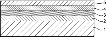
- FIG. 1 is a schematic sectional view showing the structure of a surface-treated copper foil according to an embodiment of the present invention.
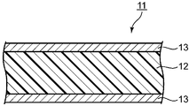
- FIG. 2 is a schematic cross-sectional view showing the configuration of a metal-clad laminate (copper-clad laminate) according to an embodiment of the present invention.
- FIG. 3 is a schematic cross-sectional view showing the configuration of the wiring board according to the embodiment of the present invention.
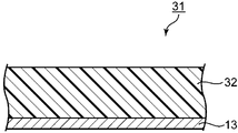
- FIG. 4 is a schematic cross-sectional view showing the configuration of the resin-coated copper foil according to the embodiment of the present invention.
- the copper-clad laminate according to one aspect of the present invention is a copper-clad laminate including an insulating layer made of a cured product of a resin composition and a surface-treated copper foil in contact with one side or both sides of the insulating layer.
- a resin-coated copper foil according to another aspect of the present invention is a resin-coated copper foil comprising a resin layer containing a resin composition or a semi-cured product of the resin composition, and a surface-treated copper foil in contact with one surface of the resin layer. It is copper foil.
- the transmission loss of a high-speed signal transmission board can be reduced, and the copper clad laminated board excellent in adhesiveness and heat resistance, the resin-coated copper foil, and a highly reliable circuit using them.
- a substrate can be provided.
- each configuration of the copper clad laminate and the resin-coated copper foil according to the present embodiment will be specifically described.
- Each reference numeral in each drawing indicates the following: 11 copper clad laminate, 12, 32 insulating layer, 13 surface-treated copper foil, 14 wiring, 21 wiring board, 31 resin-coated copper foil.
- the copper-clad laminate 11 of the present embodiment is in contact with an insulating layer 12 made of a cured product of a resin composition described below and one side or both sides of the insulating layer 12. And a copper foil 13 to be described. With such a configuration, it is possible to provide a highly reliable copper-clad laminate with reduced adhesiveness and heat resistance and reduced transmission loss.
- a cured product of the resin composition refers to a cured product that has not melted even when heated due to the progress of curing reaction and crosslinking of the resin.
- the semi-cured product of the resin composition is a state in which the resin composition is partially cured to the extent that it can be further cured. That is, the semi-cured product is a semi-cured resin composition (B-staged).
- B-staged a semi-cured resin composition
- the semi-curing there may be mentioned a state in which the viscosity starts to rise and before the curing is completed.
- the insulating layer of the copper clad laminate of the present embodiment is made of a cured product of the resin composition described below. Further, the insulating layer may include a glass base material described later. The thickness of the insulating layer is not particularly limited, but is about 20 to 800 ⁇ m.
- the resin composition forming the insulating layer of the present embodiment is a resin composition containing a compound having at least one group represented by the following formula (1) or (2) in the molecule and a crosslinking type curing agent. ..
- the compound used in this embodiment is not particularly limited as long as it is a compound having a group represented by the above formula (1) or (2), and examples thereof include polyphenylene ether resin.
- a modified polyphenylene ether compound end-modified with the group represented by the above formula (1) or (2) it is preferable to include a modified polyphenylene ether compound end-modified with the group represented by the above formula (1) or (2).
- a laminate having excellent low dielectric properties such as low dielectric constant and dielectric loss tangent can be obtained, which is very useful as various electronic materials.
- s represents an integer of 0-10.
- Z represents an arylene group.
- R 1 to R 3 are independent of each other. That is, R 1 to R 3 may be the same group or different groups. Further, R 1 to R 3 represent a hydrogen atom or an alkyl group.
- the arylene group is not particularly limited. Examples of this arylene group include a monocyclic aromatic group such as a phenylene group, and a polycyclic aromatic group in which the aromatic is not a monocyclic ring but a polycyclic aromatic group such as a naphthalene ring.
- the arylene group also includes a derivative in which a hydrogen atom bonded to an aromatic ring is substituted with a functional group such as an alkenyl group, an alkynyl group, a formyl group, an alkylcarbonyl group, an alkenylcarbonyl group, or an alkynylcarbonyl group. ..
- the alkyl group is not particularly limited, and for example, an alkyl group having 1 to 18 carbon atoms is preferable, and an alkyl group having 1 to 10 carbon atoms is more preferable. Specific examples include a methyl group, an ethyl group, a propyl group, a hexyl group, and a decyl group.
- R 4 represents a hydrogen atom or an alkyl group.
- the alkyl group is not particularly limited, and for example, an alkyl group having 1 to 18 carbon atoms is preferable, and an alkyl group having 1 to 10 carbon atoms is more preferable. Specific examples include a methyl group, an ethyl group, a propyl group, a hexyl group, and a decyl group. Further, examples of the substituent represented by the formula (2) include an acrylate group and a methacrylate group.
- examples of the substituent containing a vinylbenzyl group include a substituent represented by the following formula (3).
- group represented by the formula (3) examples include vinylbenzyl groups (ethenylbenzyl group) such as p-ethenylbenzyl group and m-ethenylbenzyl group, vinylphenyl group, acrylate group, And a methacrylate group and the like.
- vinylbenzyl groups ethenylbenzyl group
- p-ethenylbenzyl group and m-ethenylbenzyl group vinylphenyl group, acrylate group, And a methacrylate group and the like.
- the modified polyphenylene ether compound has a polyphenylene ether chain in the molecule and, for example, preferably has a repeating unit represented by the following formula (4) in the molecule.
- t represents 1 to 50.
- R 5 to R 8 are independent of each other. That is, R 5 to R 8 may be the same group or different groups.
- R 5 to R 8 represent a hydrogen atom, an alkyl group, an alkenyl group, an alkynyl group, a formyl group, an alkylcarbonyl group, an alkenylcarbonyl group, or an alkynylcarbonyl group. Among these, a hydrogen atom and an alkyl group are preferable.
- the alkyl group is not particularly limited, but for example, an alkyl group having 1 to 18 carbon atoms is preferable, and an alkyl group having 1 to 10 carbon atoms is more preferable. Specific examples include a methyl group, an ethyl group, a propyl group, a hexyl group, and a decyl group.
- the alkenyl group is not particularly limited, but for example, an alkenyl group having 2 to 18 carbon atoms is preferable, and an alkenyl group having 2 to 10 carbon atoms is more preferable. Specifically, examples thereof include a vinyl group, an allyl group, and a 3-butenyl group.
- the alkynyl group is not particularly limited, but for example, an alkynyl group having 2 to 18 carbon atoms is preferable, and an alkynyl group having 2 to 10 carbon atoms is more preferable. Specific examples include an ethynyl group and a prop-2-yn-1-yl group (propargyl group).
- the alkylcarbonyl group is not particularly limited as long as it is a carbonyl group substituted with an alkyl group.
- an alkylcarbonyl group having 2 to 18 carbon atoms is preferable, and an alkylcarbonyl group having 2 to 10 carbon atoms is more preferable.
- Specific examples include an acetyl group, a propionyl group, a butyryl group, an isobutyryl group, a pivaloyl group, a hexanoyl group, an octanoyl group, and a cyclohexylcarbonyl group.
- the alkenylcarbonyl group is not particularly limited as long as it is a carbonyl group substituted with an alkenyl group.
- an alkenylcarbonyl group having 3 to 18 carbon atoms is preferable, and an alkenylcarbonyl group having 3 to 10 carbon atoms is more preferable.
- examples thereof include an acryloyl group, a methacryloyl group, and a crotonoyl group.
- the alkynylcarbonyl group is not particularly limited as long as it is a carbonyl group substituted with an alkynyl group.
- an alkynylcarbonyl group having 3 to 18 carbon atoms is preferable, and an alkynylcarbonyl group having 3 to 10 carbon atoms is more preferable.
- a propioloyl group and the like can be mentioned.
- the weight average molecular weight (Mw) of the modified polyphenylene ether compound used in this embodiment is not particularly limited. Specifically, it is preferably 500 to 5000, more preferably 800 to 4000, and further preferably 1000 to 3000.
- the weight average molecular weight may be measured by a general molecular weight measuring method, and specific examples thereof include a value measured by gel permeation chromatography (GPC).
- GPC gel permeation chromatography
- t is such that the weight average molecular weight of the modified polyphenylene ether compound falls within such a range. It is preferably a numerical value. Specifically, t is preferably 1 to 50.
- the weight average molecular weight of the modified polyphenylene ether compound When the weight average molecular weight of the modified polyphenylene ether compound is within such a range, it has excellent low dielectric properties that the polyphenylene ether has, and is excellent not only in heat resistance of the cured product but also in moldability. Become. This is considered to be due to the following.
- the weight average molecular weight of the ordinary polyphenylene ether is within such a range, the heat resistance of the cured product tends to be lowered because the polyphenylene ether has a relatively low molecular weight.
- the modified polyphenylene ether compound according to the present embodiment has at least an unsaturated double bond at the terminal, it is considered that a cured product having sufficiently high heat resistance can be obtained.
- the modified polyphenylene ether compound when the weight average molecular weight of the modified polyphenylene ether compound is within such a range, the modified polyphenylene ether compound has a relatively low molecular weight, and is therefore considered to have excellent moldability. Therefore, it is considered that such a modified polyphenylene ether compound is not only excellent in heat resistance of the cured product, but also excellent in moldability.
- the average number of the substituents (the number of terminal functional groups) at the molecular end of one molecule of the modified polyphenylene ether in the modified polyphenylene ether compound used in the present embodiment is not particularly limited. Specifically, it is preferably 1 to 5, more preferably 1 to 3, and even more preferably 1.5 to 3. If the number of terminal functional groups is too small, it tends to be difficult to obtain a cured product having sufficient heat resistance. Further, if the number of terminal functional groups is too large, the reactivity becomes too high, and for example, the storage stability of the resin composition may be deteriorated, or the fluidity of the resin composition may be deteriorated. ..
- the number of terminal functional groups of the modified polyphenylene ether compound may be a numerical value representing the average value of the above-mentioned substituents per molecule of all modified polyphenylene ether compounds present in 1 mol of the modified polyphenylene ether compound.
- the number of terminal functional groups can be measured, for example, by measuring the number of hydroxyl groups remaining in the obtained modified polyphenylene ether compound and calculating the decrease from the number of hydroxyl groups of the polyphenylene ether before modification.
- the amount of decrease from the number of hydroxyl groups of the polyphenylene ether before modification is the number of terminal functional groups.
- the number of hydroxyl groups remaining in the modified polyphenylene ether compound is measured by adding a quaternary ammonium salt (tetraethylammonium hydroxide) that associates with the hydroxyl group to a solution of the modified polyphenylene ether compound and measuring the UV absorbance of the mixed solution. By doing, you can ask.
- a quaternary ammonium salt tetraethylammonium hydroxide
- the intrinsic viscosity of the modified polyphenylene ether compound used in this embodiment is not particularly limited. Specifically, it may be 0.03 to 0.12 dl/g, preferably 0.04 to 0.11 dl/g, and more preferably 0.06 to 0.095 dl/g. .. If the intrinsic viscosity is too low, the molecular weight tends to be low, and low dielectric properties such as low dielectric constant and low dielectric loss tangent tend to be difficult to obtain. On the other hand, if the intrinsic viscosity is too high, the viscosity is high, sufficient fluidity cannot be obtained, and the moldability of the cured product tends to decrease. Therefore, when the intrinsic viscosity of the modified polyphenylene ether compound is within the above range, excellent heat resistance and moldability of the cured product can be realized.
- the intrinsic viscosity here is an intrinsic viscosity measured in methylene chloride at 25° C., and more specifically, for example, a 0.18 g/45 ml methylene chloride solution (liquid temperature 25° C.) is measured with a viscometer. These are the values measured in. Examples of this viscometer include AVS500 Visco System manufactured by Schott.
- modified polyphenylene ether compounds include, for example, modified polyphenylene ether compounds represented by the following formula (5) and modified polyphenylene ether compounds represented by the following formula (6).
- modified polyphenylene ether compound these modified polyphenylene ether compounds may be used alone, or two kinds of modified polyphenylene ether compounds may be used in combination.
- R 9 to R 16 and R 17 to R 24 are each independently a hydrogen atom, an alkyl group, an alkenyl group, an alkynyl group, a formyl group, an alkylcarbonyl group, an alkenylcarbonyl. Group or an alkynylcarbonyl group.
- X 1 and X 2 are each independently a group represented by the above formula (1) or (2).
- a and B each represent a repeating unit represented by the following formula (7) and the following formula (8).
- Y represents a linear, branched or cyclic hydrocarbon having 20 or less carbon atoms.
- R 25 to R 28 and R 29 to R 32 each independently represent a hydrogen atom, an alkyl group, an alkenyl group, an alkynyl group, a formyl group, an alkylcarbonyl group, an alkenylcarbonyl group, or an alkynylcarbonyl group.
- the modified polyphenylene ether compound represented by the formula (5) and the modified polyphenylene ether compound represented by the formula (6) are not particularly limited as long as they are compounds satisfying the above constitution.
- R 9 to R 16 and R 17 to R 24 are independent of each other as described above. That is, R 9 to R 16 and R 17 to R 24 may be the same group or different groups.
- R 9 to R 16 and R 17 to R 24 represent a hydrogen atom, an alkyl group, an alkenyl group, an alkynyl group, a formyl group, an alkylcarbonyl group, an alkenylcarbonyl group, or an alkynylcarbonyl group.
- a hydrogen atom and an alkyl group are preferable.
- m and n each represent 0 to 20, as described above. Further, it is preferable that m and n represent numerical values such that the total value of m and n is 1 to 30. Therefore, it is more preferable that m represents 0 to 20, n represents 0 to 20, and the sum of m and n represents 1 to 30. Further, R 25 to R 28 and R 29 to R 32 are independent of each other. That is, R 25 to R 28 and R 29 to R 32 may be the same group or different groups.
- R 25 to R 28 and R 29 to R 32 represent a hydrogen atom, an alkyl group, an alkenyl group, an alkynyl group, a formyl group, an alkylcarbonyl group, an alkenylcarbonyl group, or an alkynylcarbonyl group.
- a hydrogen atom and an alkyl group are preferable.
- R 9 to R 32 are the same as R 5 to R 8 in the above formula (4).
- Y is a linear, branched, or cyclic hydrocarbon having 20 or less carbon atoms, as described above.
- Examples of Y include a group represented by the following formula (9) and the like.
- R 33 and R 34 each independently represent a hydrogen atom or an alkyl group.
- the alkyl group include a methyl group and the like.
- examples of the group represented by the formula (9) include a methylene group, a methylmethylene group, and a dimethylmethylene group. Among these, the dimethylmethylene group is preferable.
- X 1 and X 2 are each independently a group represented by the formula (1) or the formula (2).
- X 1 and X 2 may be the same substituent or different. It may be a substituent.
- modified polyphenylene ether compound represented by the above formula (5) include a modified polyphenylene ether compound represented by the following formula (10).
- modified polyphenylene ether compound represented by the formula (6) include, for example, a modified polyphenylene ether compound represented by the following formula (11) and a modified polyphenylene ether represented by the following formula (12). A compound etc. are mentioned.
- m and n are the same as m and n in the formulas (7) and (8).
- R 1 ⁇ R 3 and s are the same as R 1 ⁇ R 3 and s in the formula (1).
- Y is the same as Y in the above (6).
- R 4 is the same as R 4 in the above formula (2).
- the average number of the substituents (the number of terminal functional groups) at the molecular end per one molecule of the modified polyphenylene ether may be in the range described above.
- the number is preferably 1 to 2, and more preferably 1.5 to 2. ..
- the method for synthesizing the modified polyphenylene ether compound used in the present embodiment is such that if a modified polyphenylene ether compound end-modified with a group represented by the formula (1) or (2) (hereinafter, also referred to as a substituent) can be synthesized, It is not particularly limited. Specifically, a method of reacting polyphenylene ether with a compound in which the above-mentioned substituent and a halogen atom are bonded can be mentioned.
- Examples of the compound in which the substituent is bonded to the halogen atom include compounds in which the substituent represented by the formulas (1) and (2) is bonded to the halogen atom.
- Specific examples of the halogen atom include a chlorine atom, a bromine atom, an iodine atom and a fluorine atom, and among these, a chlorine atom is preferable.
- Specific examples of the compound in which the substituent and the halogen atom are bonded to each other include chloromethylstyrene such as o-chloromethylstyrene, p-chloromethylstyrene and m-chloromethylstyrene.
- the polyphenylene ether as a raw material is not particularly limited as long as it can finally synthesize a predetermined modified polyphenylene ether compound.
- polyphenylene ether such as poly(2,6-dimethyl-1,4-phenylene oxide) or polyphenylene ether composed of 2,6-dimethylphenol and at least one of bifunctional phenol and trifunctional phenol is used. Examples include those containing the main component.
- the bifunctional phenol is a phenol compound having two phenolic hydroxyl groups in the molecule, and examples thereof include tetramethylbisphenol A.
- the trifunctional phenol is a phenol compound having three phenolic hydroxyl groups in the molecule.
- the polyphenylene ether compound of this embodiment preferably contains a structure derived from 2,6-dimethylphenol and a bifunctional phenol.
- the above-mentioned methods can be mentioned. Specifically, the above polyphenylene ether and the compound in which the substituent and the halogen atom are bonded are dissolved in a solvent and stirred. By doing so, the polyphenylene ether reacts with the compound in which the substituent and the halogen atom are bonded, and the modified polyphenylene ether compound used in the present embodiment is obtained.
- the alkali metal hydroxide functions as a dehydrohalogenating agent, specifically, a dehydrochlorinating agent. That is, the alkali metal hydroxide, the phenol group of the polyphenylene ether, and the compound in which the substituent and the halogen atom are bonded, desorbs the hydrogen halide, and by doing so, the phenol group of the polyphenylene ether Instead of a hydrogen atom, it is believed that the substituent is attached to the oxygen atom of the phenol group.
- the alkali metal hydroxide is not particularly limited as long as it can function as a dehalogenating agent, and examples thereof include sodium hydroxide.
- the alkali metal hydroxide is usually used in the form of an aqueous solution, specifically, as an aqueous sodium hydroxide solution.
- reaction conditions such as the reaction time and the reaction temperature vary depending on the compound in which the substituent and the halogen atom are bonded and the like, and are not particularly limited as long as the above-mentioned reaction can proceed appropriately.
- the reaction temperature is preferably room temperature to 100°C, more preferably 30 to 100°C.
- the reaction time is preferably 0.5 to 20 hours, more preferably 0.5 to 10 hours.
- the solvent used during the reaction can dissolve the polyphenylene ether and the compound in which the substituent and the halogen atom are bonded, and reacts with the polyphenylene ether and the compound in which the substituent and the halogen atom are bonded.
- the above reaction is preferably carried out in the presence of not only an alkali metal hydroxide but also a phase transfer catalyst. That is, the above reaction is preferably performed in the presence of an alkali metal hydroxide and a phase transfer catalyst. By doing so, the above reaction is considered to proceed more favorably. This is considered to be due to the following.
- the phase transfer catalyst has a function of incorporating an alkali metal hydroxide, is soluble in both a phase of a polar solvent such as water and a phase of a non-polar solvent such as an organic solvent, and has an interphase between these phases.
- phase transfer catalyst is not particularly limited, and examples thereof include quaternary ammonium salts such as tetra-n-butylammonium bromide.
- the resin composition used in this embodiment preferably contains, as the modified polyphenylene ether compound, the modified polyphenylene ether compound obtained as described above.
- examples of the cross-linking type curing agent used in the present embodiment include those capable of forming cross-linking and curing by reacting with the compound (for example, the above-mentioned polyphenylene ether compound).
- trialkyl isocyanurate compounds such as triallyl isocyanurate (TAIC), polyfunctional methacrylate compounds having two or more methacrylic groups in the molecule, and polyfunctional acrylate compounds having two or more acrylic groups in the molecule.
- TAIC triallyl isocyanurate
- polyfunctional methacrylate compounds having two or more methacrylic groups in the molecule and polyfunctional acrylate compounds having two or more acrylic groups in the molecule.
- Vinyl compounds having two or more vinyl groups in the molecule such as polybutadiene (polyfunctional vinyl compounds), styrene derivatives such as divinylbenzene and bromostyrene, allyl compounds having allyl groups in the molecule, maleimide groups in the molecule and a acenaphthylene compound having an acenaphthylene structure in the molecule such as acenaphthylene.
- a trialkenyl isocyanurate compound, a polyfunctional acrylate compound having two or more acrylic groups in the molecule, a polyfunctional methacrylate compound, and a polyfunctional vinyl compound are preferable.
- crosslinking is more suitably formed by the curing reaction, and the heat resistance of the cured product of the resin composition containing the polyphenylene ether compound according to the present embodiment can be further enhanced.
- the cross-linking curing agent the exemplified cross-linking curing agent may be used alone or in combination of two or more kinds.
- the cross-linking type curing agent the above-mentioned compound having two or more unsaturated double bonds in the molecule and a compound having one unsaturated double bond in the molecule may be used in combination.
- Specific examples of the compound having one unsaturated double bond in the molecule include a compound having one vinyl group in the molecule (monovinyl compound).
- the content ratio of the compound (for example, the above-mentioned modified polyphenylene ether compound) in the resin composition of the present embodiment is not particularly limited as long as it is a ratio capable of reacting with the cross-linking curing agent to form a cured product.
- a polyphenylene ether compound it is preferably about 30 to 95 parts by mass, and preferably 40 to 90 parts by mass, based on the total amount (100 parts by mass) of the modified polyphenylene ether compound and the cross-linking curing agent. Is more preferable, and further preferably 50 to 90 parts by mass.
- the content ratio of the cross-linking curing agent is preferably 5 to 70 parts by mass, and more preferably 10 to 60 parts by mass, based on the total amount (100 parts by mass) of the modified polyphenylene ether compound and the cross-linking curing agent. It is more preferable that the amount is 10 to 50 parts by mass. With such a content ratio, it is considered that the moldability and heat resistance of the cured product are more excellent while maintaining the excellent dielectric properties of the polyphenylene ether compound. It is considered that this is because crosslinking is more preferably formed by the curing reaction while maintaining the content of the polyphenylene ether component capable of exhibiting excellent dielectric properties.
- the resin composition used in the present embodiment may be composed of, for example, a compound and a cross-linking type curing agent, or may further contain other components.
- Other components include, for example, an inorganic filler, a flame retardant, an additive, a reaction initiator and the like.
- the total content of the compound (modified polyphenylene ether compound) and the cross-linking curing agent is preferably 30% by mass or more based on the entire resin composition, The amount is more preferably 30 to 90% by mass, further preferably 40 to 80% by mass.
- the inorganic filler that can be used in this embodiment is not particularly limited, and examples thereof include an inorganic filler that can enhance the heat resistance and flame retardancy of the cured product of the resin composition.
- an inorganic filler that can enhance the heat resistance and flame retardancy of the cured product of the resin composition.
- Specific examples include silica, alumina, talc, aluminum hydroxide, magnesium hydroxide, titanium oxide, mica, aluminum borate, barium sulfate, and calcium carbonate.
- these inorganic fillers may be used as they are, but those surface-treated with a silane coupling agent of vinylsilane type, styrylsilane type, methacrylsilane type, or acrylsilane type are particularly preferable.
- a metal-clad laminate obtained using a resin composition containing an inorganic filler surface-treated with such a silane coupling agent has high heat resistance during moisture absorption, and also tends to have high interlayer peel strength. There is.
- an inorganic filler When an inorganic filler is contained, its content is preferably 5 to 60% by mass, more preferably 10 to 60% by mass, and 15 to 50% by mass based on the entire resin composition. % Is more preferable.
- a flame retardant may be added to the resin composition according to the present embodiment in order to further enhance the flame retardancy of the cured product of the resin composition.
- the flame retardant that can be used is not particularly limited, and specific examples thereof include halogen-based flame retardants such as bromine-based flame retardants and phosphorus-based flame retardants.
- halogen-based flame retardants such as bromine-based flame retardants and phosphorus-based flame retardants.
- Specific examples of the halogen-based flame retardant include, for example, bromine-based flame retardants such as pentabromodiphenyl ether, octabromodiphenyl ether, decabromodiphenyl ether, tetrabromobisphenol A, hexabromocyclododecane, and chlorine-based flame retardants such as chlorinated paraffin. Etc.
- the phosphorus-based flame retardant for example, condensed phosphoric acid ester, phosphoric acid ester such as cyclic phosphoric acid ester, phosphazene compound such as cyclic phosphazene compound, metal phosphinic acid salt such as dialkylphosphinic acid aluminum salt, and the like.
- examples include phosphinate flame retardants, melamine phosphate, and melamine flame retardants such as melamine polyphosphate.
- a phosphine oxide compound having two or more diphenylphosphine oxide groups in the molecule can be used.
- Specific phosphine oxide compounds include xylylenebisdiphenylphosphine oxide such as paraxylylenebisdiphenylphosphine oxide, phenylenebisdiphenylphosphine oxide such as paraphenylenebisdiphenylphosphine oxide, ethylenebisdiphenylphosphine oxide, biphenylenebisdiphenylphosphine oxide. , And naphthylene bisdiphenylphosphine oxide.
- each of the flame retardants exemplified above may be used alone or in combination of two or more kinds.
- the curing reaction can proceed.
- a reaction initiator may be added.
- the reaction initiator is not particularly limited as long as it can accelerate the curing reaction between the polyphenylene ether compound and the crosslinking curing agent.
- ⁇ , ⁇ ′-bis(t-butylperoxy-m-isopropyl)benzene is preferably used. Since ⁇ , ⁇ '-bis(t-butylperoxy-m-isopropyl)benzene has a relatively high reaction initiation temperature, it suppresses the acceleration of the curing reaction at the time when it is not necessary to cure it, such as when the prepreg is dried. Therefore, it is possible to suppress deterioration of the storage stability of the polyphenylene ether resin composition. Furthermore, since ⁇ , ⁇ '-bis(t-butylperoxy-m-isopropyl)benzene has low volatility, it does not volatilize during prepreg drying or storage and has good stability. Moreover, the reaction initiator may be used alone or in combination of two or more kinds.
- additives other than the above include, for example, antifoaming agents such as silicone antifoaming agents and acrylic ester antifoaming agents, heat stabilizers, antistatic agents, ultraviolet absorbers, dyes and pigments, lubricants, and wet dispersions. Dispersants such as agents are listed.
- the resin composition as described above is usually prepared into a varnish and used as a resin varnish in many cases.
- a resin varnish is prepared, for example, as follows.
- the components, the cross-linking type curing agent and, if necessary, various components that can be dissolved in an organic solvent are added to the organic solvent and dissolved. At this time, you may heat as needed. Thereafter, if necessary, a component that is not dissolved in an organic solvent, an inorganic filler or the like is added, and the mixture is dispersed using a ball mill, a bead mill, a planetary mixer, a roll mill, or the like until a predetermined dispersion state is obtained.
- a resin composition having a shape of a circle is prepared.
- the organic solvent used here is not particularly limited as long as it dissolves the compound, the cross-linking curing agent and the like and does not inhibit the curing reaction. Specific examples include toluene, cyclohexanone, methyl ethyl ketone, propylene glycol monomethyl ether acetate, and the like. These may be used alone or in combination of two or more.
- the insulating layer of the present embodiment preferably further contains a glass substrate in addition to the cured product of the resin composition.
- the insulating layer of the present embodiment includes a glass base material
- it may be used as a prepreg obtained by impregnating the glass base material with the above resin composition.
- the method of producing such a prepreg include a method of impregnating a glass base material with the above-mentioned resin varnish (a resin composition prepared in the form of a varnish) and then drying.
- Impregnation of the resin varnish into the glass substrate is performed by dipping and coating. This impregnation can be repeated multiple times if necessary. At this time, it is also possible to repeat impregnation using a plurality of resin varnishes having different compositions and concentrations to finally adjust the composition and the amount of resin desired.
- a glass base material impregnated with a resin varnish is heated at 80 to 170° C. for 1 to 10 minutes under desired heating conditions to form a resin layer (A stage) or a semi-cured resin layer containing a resin composition before curing. (B stage) is obtained.
- the organic solvent can be volatilized from the varnish by heating to reduce or remove the organic solvent.
- FIG. 1 Each symbol in FIG. 1 indicates the following: 1 copper foil, 2 fine roughening particle treatment layer, 3 heat resistance treatment layer, 4 rust prevention treatment layer, 5 silane coupling agent layer.
- the surface-treated copper foil according to the present embodiment is, as shown in FIG. 1, a surface-treated copper foil having a copper fine-roughened particle treatment layer 2 on at least one surface side of the copper foil 1, wherein The grained particle treatment layer 2 is composed of fine copper particles having a particle diameter of 40 to 200 nm, the heat treatment layer 3 containing nickel is provided on the fine grained particle treatment layer 2, and at least the heat treatment layer 3 is provided.
- a rust preventive treatment layer 4 containing chromium, a silane coupling agent treatment layer 5 on the rust preventive treatment layer, and a nickel adhesion amount in the heat resistant treatment layer is 30 to 60 mg/m 2 . It is characterized by
- the adhesion to the resin base material is increased by providing the finely-roughened particle treatment layer composed of the finely-roughened particles on the surface of the untreated copper foil, and the size of the finely-roughened particles is further.
- the amount of nickel deposited in the heat-resistant treatment layer both the transmission characteristics and the basic characteristics (adhesion with the resin substrate and heat resistance) can be achieved.
- the copper foil used for the rigid board or the like is generally an electrolytic copper foil
- the copper foil used for the flexible board or the like is generally a rolled copper foil, but in recent years, especially with the rise of the flexible board market, Electrolytic copper foils having characteristics comparable to rolled copper foils have been developed, and currently rolled copper foils and electrolytic copper foils are used regardless of the type of substrate. Therefore, the untreated copper foil used in this embodiment is not limited to the rolled copper foil or the electrolytic copper foil, and any copper foil may be used.
- the micro-roughened particle treatment layer is a first surface treatment layer formed on the untreated copper foil, and is a layer provided to increase the surface area and improve the peel strength from the resin base material. It is composed of fine copper particles having a particle diameter of 40 to 200 nm.
- the above particle size is used in the following meaning. That is, using a field emission scanning electron microscope FE-SEM (JSM-7800F manufactured by JEOL Ltd.), the sample stage was observed at a magnification of 80,000 while tilting the sample stage by 40°, and the height of the observed copper particles was measured as particles. The value of the diameter.
- the particle diameter of the fine copper particles in the finely-roughened particle treatment layer of the present embodiment is 200 nm at the maximum value and 40 nm at the minimum value in the range observed and measured by the above method.
- the fine copper particle treatment layer in the present embodiment does not exclude the inclusion of copper particles having a particle diameter of more than 200 nm or less than 40 nm. However, if the number of particles exceeds 200 nm is large, the transmission loss may increase, and if the number of particles less than 40 nm is large, sufficient adhesion may not be ensured, which is not preferable.
- the treated layer of fine copper particles in the present embodiment preferably contains 90% or more, more preferably 95% or more, of copper particles having a particle diameter of 40 to 200 nm.
- the fine-roughened particle treatment layer can be formed by an electrolytic plating method.
- the particle size of the fine copper particles of this embodiment is strongly influenced by the electrolytic composition and the bath composition of the plating process.
- the electrolytic current density when the electrolytic current density is high, the particle diameter of the roughened particles tends to be small, and conversely, when the electrolytic current density is low, the particle diameter of the roughened particles tends to be large. Therefore, in order to obtain the roughened particles having the target particle diameter, the electrolytic current density must be set appropriately.
- bath compositions and electrolysis conditions for forming a copper fine-roughened particle treatment layer are examples of bath compositions and electrolysis conditions for forming a copper fine-roughened particle treatment layer, but the present invention is not particularly limited thereto.
- Copper sulfate pentahydrate 10 to 70 g/L (particularly preferably 30 to 50 g/L) Diethylenetriamine pentaacetic acid pentasodium (hereinafter DTPA/5Na): 50 to 150 g/L (particularly preferably 80 to 120 g/L) pH: 3.0 to 6.0 (particularly preferably 3.5 to 5.5)
- DTPA/5Na Diethylenetriamine pentaacetic acid pentasodium
- DTPA/5Na 50 to 150 g/L (particularly preferably 80 to 120 g/L) pH: 3.0 to 6.0 (particularly preferably 3.5 to 5.5)
- Use sulfuric acid and sodium hydroxide to adjust pH (electrolysis conditions)
- Current density 0.5 to 10.0 A/dm 2 (particularly preferably 1.0 to 6.0 A/dm 2 )
- Electricity 10 to 130 A ⁇ sec/dm 2 (particularly preferably 30 to 110 A ⁇ sec/dm 2 )
- Liquid temperature 25 to 50°C
- a suitable DTPA/5Na concentration is 50 to 150 g/L, but outside this range, if it is less than 50 g/L, it is difficult to obtain a sufficient refining effect and the roughened particles become coarse. If it exceeds 150 g/L, the current efficiency is lowered, the precipitation amount of the roughening treatment is extremely reduced, and the voltage is further increased, which is uneconomical.
- the amount of electricity is preferably 10 to 130 A ⁇ sec/dm 2 , and in this range, there is an advantage that copper particles having a particle diameter of 40 to 200 nm can be obtained and the adhesion to the resin can be easily secured.
- the quantity of electricity is less than 10 A ⁇ sec/dm 2
- the copper particles having a particle diameter of less than 40 nm increase, and the adhesion may deteriorate.
- it is more than 130 A ⁇ sec/dm 2 the particle shape is likely to be dendritic and the particle size is likely to be coarsened, resulting in low adhesion to the untreated copper foil and more powder falling off. This causes problems such as an increase in the surface roughness of the laminated surface.
- the heat resistant treatment layer is a layer for heat resistance and rust prevention that is provided to protect the copper foil including the finely grained particle treatment layer from stress such as chemicals and heat, and is also called a barrier treatment layer.
- the heat resistant treatment layer of the present embodiment contains nickel or nickel and phosphorus, and the amount of nickel deposited in the heat resistant treatment layer is 30 to 60 mg/m 2 .
- both the transmission characteristic and the basic characteristic can be achieved. If the amount of nickel adhered is less than 30 mg/m 2 , heat resistance decreases, and for example, swelling may occur at the interface between the resin and the copper foil, resulting in a decrease in adhesion, and if it exceeds 60 mg/m 2. , The transmission loss may increase. A more preferable range of the amount of nickel deposited is 40 to 50 mg/m 2 .
- the “adhesion amount” refers to the mass per unit area of nickel deposited by plating (for example, electrolytic plating method) on the side of the copper foil on which the finely-roughened particles are treated. Further, the amount of adhesion can be measured by a method of dissolving and diluting a copper foil to be treated with nitric acid or the like and analyzing the nickel concentration using an ICP emission spectroscopic analyzer.
- the heat resistant treatment layer of the present embodiment is preferably composed of nickel (Ni) or nickel (Ni) and phosphorus (P).
- the heat resistant treatment layer of the present embodiment is a second surface treatment layer formed after forming the above-mentioned fine roughened particle treatment layer, and can be formed by an electrolytic plating method.
- the amount of nickel deposited can be adjusted depending on the current conditions when performing this electrolytic plating.
- bath compositions and electrolysis conditions for forming the heat-resistant treatment layer of the present embodiment which is composed of nickel and phosphorus, but are not particularly limited thereto.
- Nickel composition Nickel sulfate hexahydrate 10 to 100 g/L (particularly preferably 20 to 60 g/L) Sodium acetate trihydrate 2-40 g/L (preferably 5-30 g/L) Sodium hypophosphite monohydrate 0.1 to 10 g/L (particularly preferably 1.0 to 6.0 g/L) pH 3.0 to 5.5 (particularly preferably 3.5 to 5.0) (Electrolysis conditions) Current density: 0.5 to 3.5 A/dm 2 (particularly preferably 1.0 to 2.0 A/dm 2 ) Electricity: 1.8 to 2.7 A ⁇ sec/dm 2 (particularly preferably 2.0 to 2.5 A ⁇ sec/dm 2 ) Liquid temperature: 25 to 50°C (particularly preferably 30 to 40°C) Anode: An insoluble electrode such as titanium coated with a platinum group oxide.
- nickel sulfate hexahydrate nickel chloride hexahydrate, nickel acetate tetrahydrate, etc.
- Sodium phosphite, sodium hypophosphite, nickel phosphite and the like can be used as the source of phosphorus ions. Further, sodium sulfate may be added to impart conductivity.
- the anticorrosion treatment layer is a layer provided to prevent oxidation during heating or storage.
- the rustproof layer of the present embodiment contains at least chromium (Cr) and is sometimes called a chromate layer. Further, it may contain zinc (Zn).
- the anticorrosion treatment layer of the present embodiment is a third surface treatment layer formed after forming the above heat-resistant treatment layer, and can be formed by an electrolytic plating method.
- the bath composition for forming the anticorrosive layer of the present embodiment may be a known bath composition, and examples thereof include bath compositions having hexavalent chromium such as chromic acid, sodium dichromate, and potassium dichromate.
- the precipitation form of chromium after the formation of the anticorrosion treatment layer is a state in which Cr(OH) 3 and Cr 2 0 3 are mixed, and there is no hexavalent chromium that adversely affects the human body, and precipitation occurs in the form of trivalent chromium.
- the chromic acid solution may be alkaline or acidic.
- an alkaline zinc chromate solution containing zinc ions and hexavalent chromium ions described in Japanese Patent Publication No. 58-15950 may be used. It is possible to improve the rustproofing property compared to the rustproofing layer.
- the electrolytic bath and the electrolytic conditions for applying the rust preventive treatment layer of the present embodiment include, for example, the following bath compositions and conditions, but are not particularly limited thereto.
- the silane coupling agent treatment layer of the present embodiment is a surface treatment layer of the fourth layer formed after forming the anticorrosion treatment layer, a layer provided to further improve the adhesion to the resin substrate. Is. Further, by providing a silane coupling agent-treated layer, not only the peel strength can be improved, but also the deterioration of the peel strength after the harsh test can be suppressed, and the rust prevention property can be further improved, which is excellent. It is a versatile copper foil for circuit boards.
- the silane coupling agent-treated layer of the present embodiment can be formed by adding an appropriate amount of a silane coupling agent to water or the like, applying the solution as an aqueous solution by dipping or spraying, and then washing and drying.
- the silane coupling agent may be selected from various types such as epoxy group, amino group, mercapto group, vinyl group, methacryloxy group and styryl group, and used. However, since they have different properties and are compatible with the base material, it is necessary to appropriately select and use them.
- Examples of the bath for forming the silane coupling agent treatment layer include the following compositions and conditions, but are not particularly limited thereto.
- the copper-clad laminate of the present embodiment includes, for example, one or a plurality of prepregs containing the resin composition as described above, and the copper foil as described above on both upper and lower surfaces or one surface of the silane coupling. It is possible to prepare a double-sided copper foil-clad or single-sided copper foil-clad laminate by stacking the agent layers so that they are in contact with the prepreg, and heat-pressing and molding the layers to integrate them.
- the heating and pressing conditions can be appropriately set depending on the thickness of the laminated plate to be manufactured, the type of the resin composition, and the like.
- the temperature is 170 to 220° C.
- the pressure is 1.5 to 5.0 MPa
- the time is 60. It can be up to 150 minutes.
- the resin-coated copper foil 31 of the present embodiment is obtained by laminating the resin layer 32 containing the resin composition or the semi-cured product of the resin composition and the copper foil 13 provided on one surface of the resin layer. (See, for example, FIG. 4). That is, the resin-coated copper foil of the present embodiment may be a resin-coated copper foil including a resin layer containing a resin composition before curing (A-stage resin composition) and a copper foil, or a resin composition. A resin-coated copper foil including a resin layer containing a semi-cured product (B-stage resin composition) and a copper foil may be used.
- the same ones as those described for the copper clad laminate can be used.
- the resin composition or a semi-cured product thereof may be the resin composition dried or heated and dried.
- the resin varnish obtained above is applied to the surface of the copper foil on which the silane coupling agent layer is formed, and then dried to semi-cure the resin composition. Methods and the like.
- the resin layer of the resin-coated copper foil usually does not include a glass substrate, application of the resin varnish to the copper foil is performed by coating or the like, but it can be repeated a plurality of times as necessary. is there. Further, at this time, it is possible to repeat the application using a plurality of resin varnishes having different compositions and concentrations to finally adjust the composition (content ratio) and the resin amount to a desired value.
- the resin layer (A stage) containing the resin composition before curing is heated under desired heating conditions, for example, at 80 to 170° C. for 1 to 10 minutes, or A semi-cured resin layer (B stage) is obtained.
- the organic solvent can be volatilized from the varnish by heating to reduce or remove the organic solvent.
- the resin-coated copper foil of this embodiment also has the same effects and advantages as the above-mentioned copper-clad laminate.
- the copper clad laminate and the resin-coated copper foil according to the present embodiment have a conductor pattern as a circuit formed on the surface by forming a circuit by etching the copper foil on the surface of the insulating layer 12 as shown in FIG. 3, for example. It can be used as a circuit board (wiring board 21) provided with (wiring 14).
- a circuit board 21 provided with (wiring 14).
- a method of forming a circuit in addition to the method described above, for example, a circuit formation by a semi-additive method (SAP: Semi Additive Process) or a modified semi-additive method (MSAP: Modified Semi-Additive Process) can be mentioned.
- a circuit board obtained by using the copper clad laminate and the resin-coated copper foil of the present embodiment is a highly reliable circuit board having heat resistance and reduced transmission loss.
- a copper-clad laminate according to one aspect of the present invention is a copper-clad laminate comprising an insulating layer made of a cured product of a resin composition, and a surface-treated copper foil in contact with one side or both sides of the insulating layer,
- the resin composition contains a compound having at least one group represented by the following formula (1) or (2) in the molecule and a cross-linking curing agent: (In the formula (1), s represents an integer of 0 to 10. Z represents an arylene group.
- R 1 to R 3 each independently represent a hydrogen atom or an alkyl group.
- R 4 represents a hydrogen atom or an alkyl group
- the surface-treated copper foil is a surface-treated copper foil having a copper fine-roughened particle treatment layer on at least one surface side of the copper foil, the fine-roughened particle treatment layer having a particle diameter of 40 to 200 nm.
- It is composed of fine copper particles, has a heat-resistant treatment layer containing nickel on the fine roughened particle treatment layer, has a rust-proof treatment layer containing at least chromium on the heat-resistant treatment layer, the rust-prevention treatment
- a silane coupling agent layer is provided on the layer, and the amount of nickel deposited in the heat resistant treatment layer is 30 to 60 mg/m 2 .
- the compound contains a modified polyphenylene ether compound which is end-modified with a group represented by the formula (1) or (2).
- the modified polyphenylene ether compound preferably has a weight average molecular weight (Mw) of 500 to 5,000. Therefore, it is considered that the above effect can be obtained more reliably.
- the content of the compound contained in the resin composition of the insulating layer is 30 to 95 parts by mass with respect to 100 parts by mass of the total amount of the compound and the cross-linking curing agent. preferable. Therefore, it is considered that the above effect can be obtained more reliably.
- the cross-linking type curing agent is a trialkenyl isocyanurate compound, a polyfunctional acrylate compound having two or more acrylic groups in the molecule, or a polyfunctional methacrylate having two or more methacrylic groups in the molecule.
- the polyphenylene ether compound preferably contains a structure derived from 2,6-dimethylphenol and a bifunctional phenol, and the group represented by the formula (1) is a p-ethenylbenzyl group or m- It preferably contains at least one selected from the group consisting of ethenylbenzyl groups.
- the heat-resistant treatment layer is composed of nickel or nickel and phosphorus. As a result, the effects as described above can be obtained more reliably.
- a resin-coated copper foil according to a further aspect of the present invention includes a resin layer containing a resin composition as described above or a semi-cured product of the resin composition, and the surface-treated copper foil described above on one surface of the resin layer. It is characterized by
- the present invention also includes a circuit board including the copper clad laminate or the resin-coated copper foil, and having a conductor pattern as a circuit on the surface thereof.
- the present invention provides a resin composition for forming an insulating layer in a copper-clad laminate comprising an insulating layer made of a cured product of a resin composition and a surface-treated copper foil in contact with one side or both sides of the insulating layer. And containing a compound having at least one group represented by the following formula (1) or (2) in the molecule and a cross-linking curing agent: (In the formula (1), s represents an integer of 0 to 10. Z represents an arylene group.
- R 1 to R 3 each independently represent a hydrogen atom or an alkyl group.
- R 4 represents a hydrogen atom or an alkyl group
- the surface-treated copper foil is a surface-treated copper foil having a copper fine-roughened particle treatment layer on at least one surface side of the copper foil, the fine-roughened particle treatment layer having a particle diameter of 40 to 200 nm.
- It is composed of particles, having a heat treatment layer containing nickel on the fine roughening particle treatment layer, An anticorrosion treatment layer containing at least chromium is provided on the heat resistance treatment layer, a silane coupling agent layer is provided on the anticorrosion treatment layer, and the amount of nickel deposited in the heat treatment treatment layer is 30 to 60 mg/ Also included is a resin composition characterized by having m 2 .
- Modified polyphenylene ether 1 (modified PPE1) was obtained by reacting polyphenylene ether and chloromethylstyrene.
- polyphenylene ether polyphenylene ether, SA90 manufactured by SABIC Innovative Plastics, the number of terminal hydroxyl groups
- the obtained solid was analyzed by 1 H-NMR (400 MHz, CDCl 3 , TMS). As a result of NMR measurement, a peak derived from ethenylbenzyl was confirmed at 5 to 7 ppm. This confirmed that the obtained solid was ethenylbenzylated polyphenylene ether.
- the polyphenylene ether used was SA120 (intrinsic viscosity (IV) 0.125 dl/g, one terminal hydroxyl group, weight average molecular weight Mw3100) manufactured by SABIC Innovative Plastics.
- SA9000 SABIC manufactured by SABIC Innovative Plastics SA9000 (terminal methacryl group-modified PPE, weight average molecular weight (Mw) 2000)
- SA90 SAB manufactured by SABIC Innovative Plastics (unmodified PPE, weight average molecular weight (Mw) 1700)
- -Crosslinking type curing agent TAIC (triallyl isocyanurate, manufactured by Nippon Kasei Co., Ltd.)
- Reaction initiator Perbutyl P: 1,3-di(t-butylperoxyisopropyl)benzene (Perbutyl P manufactured by NOF CORPORATION)
- a copper fine-roughened particle treatment layer was formed on the laminate surface side of the untreated copper foil by treating it with the bath composition and electrolysis conditions shown below.
- the obtained micro-roughened particle treatment layer was observed with a field emission scanning electron microscope FE-SEM (JSM-7800F manufactured by JEOL Ltd.) at a magnification of 80,000 while tilting the sample stage by 40°.
- the height of the copper particles observed as a result was used as the value of the particle diameter, and the particle diameter of the roughened particles in the fine roughened particle treatment layer was a minimum value of 40 nm and a maximum value of 200 nm.
- a heat-resistant treatment layer which is the second surface treatment layer, was formed by treating it with the bath composition and electrolysis conditions shown below.
- Nickel composition Nickel sulfate hexahydrate 30 g/L Sodium acetate trihydrate 10 g/L Sodium hypophosphite monohydrate 2.0 g/L (Electrolysis conditions) Current density: 1.6 A/dm 2 Electricity: 2.7 Asec/dm 2 pH 4.5 Liquid temperature: 32°C Anode: Platinum group oxide coated titanium plate.
- the amount of nickel deposited on the obtained heat-resistant treated layer was measured by dissolving and diluting the treated copper foil with nitric acid and analyzing the concentration of nickel with an ICP emission spectroscopic analyzer. As a result, the amount of deposited nickel was 56 mg/m 2 .
- the rust-preventive treatment layer which is the third surface treatment layer, was treated with the following electrolytic bath composition, pH, and electrolysis conditions.
- a silane coupling agent-treated layer to be the fourth layer surface-treated layer is formed by treatment with the bath composition, liquid temperature, and immersion time shown below to form the surface-treated copper foil of Example 1. Obtained.
- a surface-treated copper foil 2 was obtained in the same manner as the surface-treated copper foil 1, except that the second heat-resistant treatment layer was formed by treatment under the bath composition and electrolysis conditions shown below.
- the amount of nickel deposited on the obtained heat-resistant treatment layer was 32 mg/m 2 .
- a surface-treated copper foil 3 was obtained in the same manner as the surface-treated copper foil 1, except that the second heat-resistant treatment layer was not provided.
- the amount of nickel deposited on the obtained surface-treated copper foil 3 was 0 mg/m 2 .
- a surface-treated copper foil 4 was obtained in the same manner as the surface-treated copper foil 1, except that the second heat-resistant treatment layer was formed by treating under the bath composition and electrolysis conditions shown below.
- the amount of nickel deposited on the obtained heat-resistant treatment layer was 82 mg/m 2 .
- Nickel composition Nickel sulfate hexahydrate 30 g/L Sodium acetate trihydrate 10 g/L Sodium hypophosphite monohydrate 2.0 g/L (Electrolysis conditions) Current density: 2.1 A/dm 2 Electricity: 3.6 Asec/dm 2 pH 4.5 Liquid temperature: 32°C Anode: Platinum group oxide coated titanium plate.
- a surface-treated copper foil 6 was obtained in the same manner as the surface-treated copper foil 1, except that the first layer of finely-roughened particle-treated layer was formed by treatment under the bath composition and electrolysis conditions shown below.
- the particle diameter of the roughened particles in the obtained fine roughened particle-treated layer was 700 nm in the minimum value and 1400 nm in the maximum value.
- the amount of nickel deposited on the obtained heat resistant treatment layer was 32 mg/m 2 .
- Electrolysis conditions After electrolyzing in the bath (1) under the electrolysis conditions of a current density of 50 A/dm 2 , an electric quantity of 130 A ⁇ sec/dm 2 , and a liquid temperature of 30° C., fine copper particles are attached, and then in the bath (2).
- a fine roughened particle treatment layer was formed by electrolysis under a current density of 5 A/dm 2 , an electric quantity of 400 A ⁇ sec/dm 2 , and a liquid temperature of 40° C. for electrolysis.
- Nickel composition Nickel sulfate hexahydrate 30 g/L Sodium acetate trihydrate 10 g/L Sodium hypophosphite monohydrate 2.0 g/L (Electrolysis conditions) Current density: 1.3 A/dm 2 Electricity: 2.3 A ⁇ sec/dm 2 pH 4.5 Liquid temperature: 32°C Anode: Platinum group oxide coated titanium plate.
- the passage loss was evaluated using a network analyzer (N5230A manufactured by Keysight Technologies, Inc.).
- the evaluation frequency was 20 GHz.
- Table 1 shows the above test results.
- Comparative Example 4 in which the copper particle size in the finely-roughened particle treatment layer was large, the transmission characteristics were inferior and the heat resistance was not sufficient. Even in Comparative Example 5 in which the rustproof layer was not formed, sufficient heat resistance could not be obtained.
- the present invention has a wide range of industrial applicability in the technical field of electronic materials for transmission boards (circuit boards) and various devices using the same.
Landscapes
- Chemical & Material Sciences (AREA)
- Engineering & Computer Science (AREA)
- Organic Chemistry (AREA)
- Chemical Kinetics & Catalysis (AREA)
- Electrochemistry (AREA)
- Metallurgy (AREA)
- Materials Engineering (AREA)
- Microelectronics & Electronic Packaging (AREA)
- Medicinal Chemistry (AREA)
- Polymers & Plastics (AREA)
- Health & Medical Sciences (AREA)
- Manufacturing & Machinery (AREA)
- Inorganic Chemistry (AREA)
- Laminated Bodies (AREA)
- Parts Printed On Printed Circuit Boards (AREA)
- Manufacturing Of Printed Wiring (AREA)
- Compositions Of Macromolecular Compounds (AREA)
Abstract
本発明は、高速信号伝送基板の伝送損失を低減させることができ、かつ、密着性と耐熱性に優れる銅張積層板等を提供することを目的とする。 樹脂組成物の硬化物からなる絶縁層と、前記絶縁層に接する表面処理銅箔とを備える銅張積層板であって、前記樹脂組成物が、本願所定の基を少なくとも1つ有する化合物と架橋型硬化剤とを含むこと、並びに、前記表面処理銅箔が、銅箔(1)の少なくとも一方の面側に銅の微細粗化粒子処理層(2)を有する表面処理銅箔であって、前記微細粗化粒子処理層が粒子径40~200nmの微細銅粒子で構成されており、前記微細粗化粒子処理層上にニッケルを含む耐熱処理層(3)を有し、前記耐熱処理層上に少なくともクロムを含む防錆処理層(4)を有し、前記防錆処理層上にシランカップリング剤層(5)を有し、かつ、前記耐熱処理層中のニッケル付着量が30~60mg/m2であることを特徴とする、銅張積層板に関する。
Description
本発明は、銅張積層板、樹脂付銅箔、および、それらを用いた回路基板に関する。
高周波対応の高速信号伝送基板には、導体として各種の金属箔、特に銅箔が使用されているが、将来的には、現在よりもさらに高い周波数の信号を使用する5GやWiGig(Wireless Gigabit)等に対応する必要がある。そのため、基板の伝送損失をより低減することが求められている。
このような問題において、伝送損失を低減するためには、基板を構成する樹脂基材と銅箔を改良する必要がある。つまり、樹脂基材の誘電体に起因する伝送損失を小さくし、さらに銅箔の導体損失を小さくすることが必要となっている。
このうち銅箔側の改良については、従来、表面粗さを小さくする等によって導体損失の低減を図ってきた。しかし、表面粗さを小さくすると、基板に用いられる銅箔の基本特性として必須である樹脂との密着性や耐熱性が下がり、表面粗さを大きくすると伝送損失が大きくなるという問題があり、伝送特性と基本特性を両立させるのは難しいとされていた。これは、粗度を小さくすると樹脂との接着面積が減りアンカー効果による密着が得られにくくなって、その結果、ピール強度が低くなり耐熱も悪くなり、粗度を大きくすると銅箔表面を流れる電流の抵抗が大きくなり、伝送損失が大きくなるためと考えられる。
その他にも、高周波信号伝送回路形成用表面処理銅箔としては、伝送特性に影響を及ぼす粗化処理層について、従来の金属銅ではなく不導体の銅複合化合物で構成することで電気が流れないようにして粗化処理による導電損失を低減することが報告されている(特許文献1)。
また、プリント配線板用表面処理銅箔において、伝送特性に影響を及ぼすシランカップリング剤層の粗化粒子の平均高さを調節したり、ニッケルを含む金属処理層のニッケル元素量を調節したりすることも知られている(特許文献2)。
しかしながら、上記特許文献1記載の技術では、バリア処理やクロメート処理等を行わないため、特に耐熱性に劣るという問題がある。
一方、上記特許文献2記載の技術では、バリア処理層として機能する金属処理層の処理量が少ないため、高い温度域(例えば、150℃以上)では耐熱性の確保が困難になるという問題がある。
本発明は、かかる事情に鑑みてなされたものであって、高速信号伝送基板の伝送損失を低減させることができ、かつ、密着性と耐熱性に優れる銅張積層板、樹脂付銅箔、並びにそれらを用いた信頼性の高い回路基板を提供することを目的とする。
本発明の一態様に係る銅張積層板は、樹脂組成物の硬化物からなる絶縁層と、前記絶縁層の片面又は両面に接する表面処理銅箔とを備える銅張積層板であって、前記樹脂組成物が、分子中に下記式(1)または(2)で表される基を少なくとも1つ有する化合物と架橋型硬化剤とを含むこと、
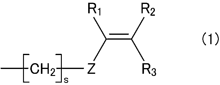
(式(1)中、sは0~10の整数を示す。また、Zは、アリーレン基を示す。また、R1~R3は、それぞれ独立して、水素原子又はアルキル基を示す)

(式(2)中、R4は、水素原子又はアルキル基を示す)
並びに、前記表面処理銅箔が、銅箔の少なくとも一方の面側に銅の微細粗化粒子処理層を有する表面処理銅箔であって、前記微細粗化粒子処理層が粒子径40~200nmの微細銅粒子で構成されており、前記微細粗化粒子処理層上にニッケルを含む耐熱処理層を有し、前記耐熱処理層上に少なくともクロムを含む防錆処理層を有し、前記防錆処理層上にシランカップリング剤層を有し、かつ、前記耐熱処理層中のニッケル付着量が30~60mg/m2であることを特徴とする。
並びに、前記表面処理銅箔が、銅箔の少なくとも一方の面側に銅の微細粗化粒子処理層を有する表面処理銅箔であって、前記微細粗化粒子処理層が粒子径40~200nmの微細銅粒子で構成されており、前記微細粗化粒子処理層上にニッケルを含む耐熱処理層を有し、前記耐熱処理層上に少なくともクロムを含む防錆処理層を有し、前記防錆処理層上にシランカップリング剤層を有し、かつ、前記耐熱処理層中のニッケル付着量が30~60mg/m2であることを特徴とする。
また、本発明の他の局面に係る樹脂付銅箔は、樹脂組成物又は前記樹脂組成物の半硬化物を含む樹脂層と、前記樹脂層の片面に接する表面処理銅箔とを備える樹脂付銅箔であって、前記樹脂組成物が、分子中に下記式(1)または(2)で表される基を少なくとも1つ有する化合物と架橋型硬化剤とを含むこと、
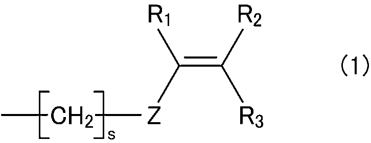
(式(1)中、sは0~10の整数を示す。また、Zは、アリーレン基を示す。また、R1~R3は、それぞれ独立して、水素原子又はアルキル基を示す)
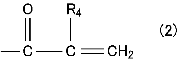
(式(2)中、R4は、水素原子又はアルキル基を示す)
並びに、前記表面処理銅箔が、銅箔の少なくとも一方の面側に銅の微細粗化粒子処理層を有する表面処理銅箔であって、前記微細粗化粒子処理層が粒子径40~200nmの微細銅粒子で構成されており、前記微細粗化粒子処理層上にニッケルを含む耐熱処理層を有し、前記耐熱処理層上に少なくともクロムを含む防錆処理層を有し、前記防錆処理層上にシランカップリング剤層を有し、かつ、前記耐熱処理層中のニッケル付着量が30~60mg/m2であることを特徴とする。
並びに、前記表面処理銅箔が、銅箔の少なくとも一方の面側に銅の微細粗化粒子処理層を有する表面処理銅箔であって、前記微細粗化粒子処理層が粒子径40~200nmの微細銅粒子で構成されており、前記微細粗化粒子処理層上にニッケルを含む耐熱処理層を有し、前記耐熱処理層上に少なくともクロムを含む防錆処理層を有し、前記防錆処理層上にシランカップリング剤層を有し、かつ、前記耐熱処理層中のニッケル付着量が30~60mg/m2であることを特徴とする。
本発明の一態様に係る銅張積層板は、樹脂組成物の硬化物からなる絶縁層と、前記絶縁層の片面又は両面に接する表面処理銅箔とを備える銅張積層板である。また、本発明の別の態様に係る樹脂付銅箔は、樹脂組成物又は前記樹脂組成物の半硬化物を含む樹脂層と、前記樹脂層の片面に接する表面処理銅箔とを備える樹脂付銅箔である。
本発明によれば、高速信号伝送基板の伝送損失を低減させることができ、かつ、密着性と耐熱性に優れる銅張積層板、樹脂付銅箔、および、それらを用いた信頼性の高い回路基板を提供することができる。
以下、本実施形態に係る銅張積層板および樹脂付銅箔の各構成について、具体的に説明する。なお、各図面(図2~4)における各符号は以下を示す:11 銅張積層板、12、32 絶縁層、13 表面処理銅箔、14 配線、21 配線基板、31 樹脂付き銅箔。
<銅張積層板>
本実施形態の銅張積層板11は、図2に示すように、以下に説明する樹脂組成物の硬化物からなる絶縁層12と、前記絶縁層12の片面又は両面に接している、以下に説明する銅箔13とを備えることを特徴とする。このような構成により、密着性や耐熱性を備えつつ、伝送損失が低減された、信頼性の高い銅張積層板を提供することができる。
本実施形態の銅張積層板11は、図2に示すように、以下に説明する樹脂組成物の硬化物からなる絶縁層12と、前記絶縁層12の片面又は両面に接している、以下に説明する銅箔13とを備えることを特徴とする。このような構成により、密着性や耐熱性を備えつつ、伝送損失が低減された、信頼性の高い銅張積層板を提供することができる。
<絶縁層>
まず、本実施形態において、樹脂組成物の硬化物とは硬化反応が進行し、樹脂が架橋することにより、加熱しても溶融しない状態となったもののことをさす。また、樹脂組成物の半硬化物とは、樹脂組成物を、さらに硬化しうる程度に途中まで硬化された状態のものである。すなわち、半硬化物は、樹脂組成物を半硬化した状態の(Bステージ化された)ものである。例えば、樹脂組成物は、加熱すると、最初、粘度が徐々に低下し、その後、硬化が開始し、粘度が徐々に上昇する。このような場合、半硬化としては、粘度が上昇し始めてから、完全に硬化する前の間の状態等が挙げられる。
まず、本実施形態において、樹脂組成物の硬化物とは硬化反応が進行し、樹脂が架橋することにより、加熱しても溶融しない状態となったもののことをさす。また、樹脂組成物の半硬化物とは、樹脂組成物を、さらに硬化しうる程度に途中まで硬化された状態のものである。すなわち、半硬化物は、樹脂組成物を半硬化した状態の(Bステージ化された)ものである。例えば、樹脂組成物は、加熱すると、最初、粘度が徐々に低下し、その後、硬化が開始し、粘度が徐々に上昇する。このような場合、半硬化としては、粘度が上昇し始めてから、完全に硬化する前の間の状態等が挙げられる。
本実施形態の銅張積層板が備える絶縁層は、下記で説明する樹脂組成物の硬化物からなる。さらに、絶縁層が後述するガラス基材を含んでいてもよい。絶縁層の厚みは、特に限定されないが、20~800μm程度である。
本実施形態の絶縁層を構成する樹脂組成物は、分子中に下記式(1)または(2)で表される基を少なくとも1つ有する化合物と架橋型硬化剤とを含む樹脂組成物である。


本実施形態において用いられる化合物は、前記式(1)または(2)で表される基を有する化合物であれば特に限定はなく、例えば、ポリフェニレンエーテル樹脂等が挙げられる。
中でも、前記式(1)または(2)で表される基によって、末端変性された変性ポリフェニレンエーテル化合物を含むことが好ましい。それによって、低い誘電率と誘電正接という優れた低誘電特性を有する積層板を得ることができ、各種電子材料として非常に有用である。
前記式(1)中、sは0~10の整数を示す。また、Zは、アリーレン基を示す。また、R1~R3は、それぞれ独立している。すなわち、R1~R3は、それぞれ同一の基であっても、異なる基であってもよい。また、R1~R3は、水素原子又はアルキル基を示す。
なお、式(1)において、pが0である場合は、Zがポリフェニレンエーテルの末端に直接結合していることを示す。
このアリーレン基は、特に限定されない。このアリーレン基としては、例えば、フェニレン基等の単環芳香族基や、芳香族が単環ではなく、ナフタレン環等の多環芳香族である多環芳香族基等が挙げられる。また、このアリーレン基には、芳香族環に結合する水素原子が、アルケニル基、アルキニル基、ホルミル基、アルキルカルボニル基、アルケニルカルボニル基、又はアルキニルカルボニル基等の官能基で置換された誘導体も含む。また、前記アルキル基は、特に限定されず、例えば、炭素数1~18のアルキル基が好ましく、炭素数1~10のアルキル基がより好ましい。具体的には、例えば、メチル基、エチル基、プロピル基、ヘキシル基、及びデシル基等が挙げられる。
式(2)中、R4は、水素原子又はアルキル基を示す。前記アルキル基は、特に限定されず、例えば、炭素数1~18のアルキル基が好ましく、炭素数1~10のアルキル基がより好ましい。具体的には、例えば、メチル基、エチル基、プロピル基、ヘキシル基、及びデシル基等が挙げられる。また、前記式(2)で表される置換基としては、例えば、アクリレート基及びメタクリレート基等が挙げられる。
また、前記ビニルベンジル基を含む置換基としては、例えば、下記式(3)で表される置換基等が挙げられる。
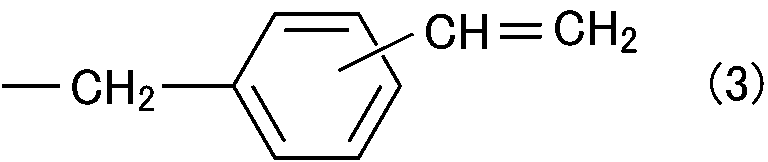
前記式(3)で示される基としては、より具体的には、p-エテニルベンジル基及びm-エテニルベンジル基等のビニルベンジル基(エテニルベンジル基)、ビニルフェニル基、アクリレート基、及びメタクリレート基等が挙げられる。
前記変性ポリフェニレンエーテル化合物は、ポリフェニレンエーテル鎖を分子中に有しており、例えば、下記式(4)で表される繰り返し単位を分子中に有していることが好ましい。
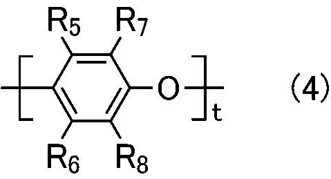
式(4)において、tは、1~50を示す。また、R5~R8は、それぞれ独立している。すなわち、R5~R8は、それぞれ同一の基であっても、異なる基であってもよい。また、R5~R8は、水素原子、アルキル基、アルケニル基、アルキニル基、ホルミル基、アルキルカルボニル基、アルケニルカルボニル基、又はアルキニルカルボニル基を示す。この中でも、水素原子及びアルキル基が好ましい。
R5~R8において、挙げられた各官能基としては、具体的には、以下のようなものが挙げられる。
アルキル基は、特に限定されないが、例えば、炭素数1~18のアルキル基が好ましく、炭素数1~10のアルキル基がより好ましい。具体的には、例えば、メチル基、エチル基、プロピル基、ヘキシル基、及びデシル基等が挙げられる。
アルケニル基は、特に限定されないが、例えば、炭素数2~18のアルケニル基が好ましく、炭素数2~10のアルケニル基がより好ましい。具体的には、例えば、ビニル基、アリル基、及び3-ブテニル基等が挙げられる。
アルキニル基は、特に限定されないが、例えば、炭素数2~18のアルキニル基が好ましく、炭素数2~10のアルキニル基がより好ましい。具体的には、例えば、エチニル基、及びプロパ-2-イン-1-イル基(プロパルギル基)等が挙げられる。
アルキルカルボニル基は、アルキル基で置換されたカルボニル基であれば、特に限定されないが、例えば、炭素数2~18のアルキルカルボニル基が好ましく、炭素数2~10のアルキルカルボニル基がより好ましい。具体的には、例えば、アセチル基、プロピオニル基、ブチリル基、イソブチリル基、ピバロイル基、ヘキサノイル基、オクタノイル基、及びシクロヘキシルカルボニル基等が挙げられる。
アルケニルカルボニル基は、アルケニル基で置換されたカルボニル基であれば、特に限定されないが、例えば、炭素数3~18のアルケニルカルボニル基が好ましく、炭素数3~10のアルケニルカルボニル基がより好ましい。具体的には、例えば、アクリロイル基、メタクリロイル基、及びクロトノイル基等が挙げられる。
アルキニルカルボニル基は、アルキニル基で置換されたカルボニル基であれば、特に限定されないが、例えば、炭素数3~18のアルキニルカルボニル基が好ましく、炭素数3~10のアルキニルカルボニル基がより好ましい。具体的には、例えば、プロピオロイル基等が挙げられる。
本実施形態において用いられる変性ポリフェニレンエーテル化合物の重量平均分子量(Mw)は、特に限定されない。具体的には、500~5000であることが好ましく、800~4000であることがより好ましく、1000~3000であることがさらに好ましい。なお、ここで、重量平均分子量は、一般的な分子量測定方法で測定したものであればよく、具体的には、ゲルパーミエーションクロマトグラフィ(GPC)を用いて測定した値等が挙げられる。また、変性ポリフェニレンエーテル化合物が、前記式(5)で表される繰り返し単位を分子中に有している場合、tは、変性ポリフェニレンエーテル化合物の重量平均分子量がこのような範囲内になるような数値であることが好ましい。具体的には、tは、1~50であることが好ましい。
変性ポリフェニレンエーテル化合物の重量平均分子量がこのような範囲内であると、ポリフェニレンエーテルの有する優れた低誘電特性を有し、硬化物の耐熱性により優れるだけではなく、成形性にも優れたものとなる。このことは、以下のことによると考えられる。通常のポリフェニレンエーテルでは、その重量平均分子量がこのような範囲内であると、比較的低分子量のものであるので、硬化物の耐熱性が低下する傾向がある。この点、本実施形態に係る変性ポリフェニレンエーテル化合物は、末端に不飽和二重結合を以上有するので、硬化物の耐熱性が充分に高いものが得られると考えられる。また、変性ポリフェニレンエーテル化合物の重量平均分子量がこのような範囲内であると、比較的低分子量のものであるので、成形性にも優れると考えられる。よって、このような変性ポリフェニレンエーテル化合物は、硬化物の耐熱性により優れるだけではなく、成形性にも優れたものが得られると考えられる。
また、本実施形態において用いられる変性ポリフェニレンエーテル化合物における、変性ポリフェニレンエーテル1分子当たりの、分子末端に有する、前記置換基の平均個数(末端官能基数)は、特に限定されない。具体的には、1~5個であることが好ましく、1~3個であることがより好ましく、1.5~3個であることがさらに好ましい。この末端官能基数が少なすぎると、硬化物の耐熱性としては充分なものが得られにくい傾向がある。また、末端官能基数が多すぎると、反応性が高くなりすぎ、例えば、樹脂組成物の保存性が低下したり、樹脂組成物の流動性が低下してしまう等の不具合が発生するおそれがある。すなわち、このような変性ポリフェニレンエーテルを用いると、流動性不足等により、例えば、多層成形時にボイドが発生する等の成形不良が発生し、信頼性の高いプリント配線板が得られにくいという成形性の問題が生じるおそれがあった。
なお、変性ポリフェニレンエーテル化合物の末端官能基数は、変性ポリフェニレンエーテル化合物1モル中に存在する全ての変性ポリフェニレンエーテル化合物の1分子あたりの、前記置換基の平均値を表した数値等が挙げられる。この末端官能基数は、例えば、得られた変性ポリフェニレンエーテル化合物に残存する水酸基数を測定して、変性前のポリフェニレンエーテルの水酸基数からの減少分を算出することによって、測定することができる。この変性前のポリフェニレンエーテルの水酸基数からの減少分が、末端官能基数である。そして、変性ポリフェニレンエーテル化合物に残存する水酸基数の測定方法は、変性ポリフェニレンエーテル化合物の溶液に、水酸基と会合する4級アンモニウム塩(テトラエチルアンモニウムヒドロキシド)を添加し、その混合溶液のUV吸光度を測定することによって、求めることができる。
また、本実施形態において用いられる変性ポリフェニレンエーテル化合物の固有粘度は、特に限定されない。具体的には、0.03~0.12dl/gであればよいが、0.04~0.11dl/gであることが好ましく、0.06~0.095dl/gであることがより好ましい。この固有粘度が低すぎると、分子量が低い傾向があり、低誘電率や低誘電正接等の低誘電性が得られにくい傾向がある。また、固有粘度が高すぎると、粘度が高く、充分な流動性が得られず、硬化物の成形性が低下する傾向がある。よって、変性ポリフェニレンエーテル化合物の固有粘度が上記範囲内であれば、優れた、硬化物の耐熱性及び成形性を実現できる。
なお、ここでの固有粘度は、25℃の塩化メチレン中で測定した固有粘度であり、より具体的には、例えば、0.18g/45mlの塩化メチレン溶液(液温25℃)を、粘度計で測定した値等である。この粘度計としては、例えば、Schott社製のAVS500 Visco System等が挙げられる。
より具体的な変性ポリフェニレンエーテル化合物としては、例えば、下記式(5)で表される変性ポリフェニレンエーテル化合物、及び下記式(6)で表される変性ポリフェニレンエーテル化合物等が挙げられる。また、前記変性ポリフェニレンエーテル化合物としては、これらの変性ポリフェニレンエーテル化合物を単独で用いてもよいし、この2種の変性ポリフェニレンエーテル化合物を組み合わせて用いてもよい。
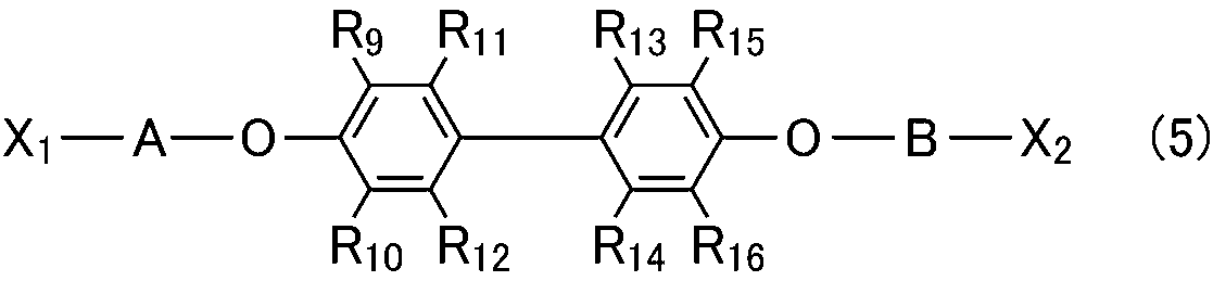

式(5)及び式(6)中、R9~R16並びにR17~R24は、それぞれ独立して、水素原子、アルキル基、アルケニル基、アルキニル基、ホルミル基、アルキルカルボニル基、アルケニルカルボニル基、又はアルキニルカルボニル基を示す。X1及びX2は、それぞれ独立して、前記式(1)または(2)で表される基である。A及びBは、それぞれ、下記式(7)及び下記式(8)で表される繰り返し単位を示す。また、式(6)中、Yは、炭素数20以下の直鎖状、分岐状、又は環状の炭化水素を示す。

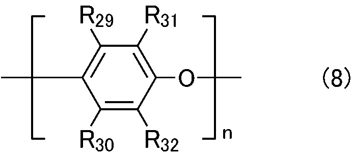
式(7)及び式(8)中、m及びnは、それぞれ、0~20を示す。R25~R28並びにR29~R32は、それぞれ独立して、水素原子、アルキル基、アルケニル基、アルキニル基、ホルミル基、アルキルカルボニル基、アルケニルカルボニル基、又はアルキニルカルボニル基を示す。
前記式(5)で表される変性ポリフェニレンエーテル化合物、及び前記式(6)で表される変性ポリフェニレンエーテル化合物は、上記構成を満たす化合物であれば特に限定されない。具体的には、前記式(5)及び前記式(6)において、R9~R16並びにR17~R24は、上述したように、それぞれ独立している。すなわち、R9~R16並びにR17~R24は、それぞれ同一の基であっても、異なる基であってもよい。また、R9~R16並びにR17~R24は、水素原子、アルキル基、アルケニル基、アルキニル基、ホルミル基、アルキルカルボニル基、アルケニルカルボニル基、又はアルキニルカルボニル基を示す。この中でも、水素原子及びアルキル基が好ましい。
また、式(7)及び式(8)中、m及びnは、それぞれ、上述したように、0~20を示すことが好ましい。さらに、m及びnは、mとnとの合計値が、1~30となる数値を示すことが好ましい。よって、mは、0~20を示し、nは、0~20を示し、mとnとの合計は、1~30を示すことがより好ましい。また、R25~R28並びにR29~R32は、それぞれ独立している。すなわち、R25~R28並びにR29~R32は、それぞれ同一の基であっても、異なる基であってもよい。また、R25~R28並びにR29~R32は、水素原子、アルキル基、アルケニル基、アルキニル基、ホルミル基、アルキルカルボニル基、アルケニルカルボニル基、又はアルキニルカルボニル基を示す。この中でも、水素原子及びアルキル基が好ましい。
R9~R32は、上記式(4)におけるR5~R8と同じである。
前記式(6)中において、Yは、上述したように、炭素数20以下の直鎖状、分岐状、又は環状の炭化水素である。Yとしては、例えば、下記式(9)で表される基等が挙げられる。

前記式(9)中、R33及びR34は、それぞれ独立して、水素原子またはアルキル基を示す。前記アルキル基としては、例えば、メチル基等が挙げられる。また、式(9)で表される基としては、例えば、メチレン基、メチルメチレン基、及びジメチルメチレン基等が挙げられ、この中でも、ジメチルメチレン基が好ましい。
前記式(5)及び前記式(6)中において、X1及びX2は、それぞれ独立して、前記式(1)または式(2)で表される基である。なお、前記式(5)で表される変性ポリフェニレンエーテル化合物及び前記式(6)で表される変性ポリフェニレンエーテル化合物において、X1及びX2は、同一の置換基であってもよいし、異なる置換基であってもよい。
前記式(5)で表される変性ポリフェニレンエーテル化合物のより具体的な例示としては、例えば、下記式(10)で表される変性ポリフェニレンエーテル化合物等が挙げられる。

前記式(6)で表される変性ポリフェニレンエーテル化合物のより具体的な例示としては、例えば、下記式(11)で表される変性ポリフェニレンエーテル化合物、下記式(12)で表される変性ポリフェニレンエーテル化合物等が挙げられる。


上記式(10)~式(12)において、m及びnは、上記式(7)及び上記式(8)におけるm及びnと同じである。また、上記式(10)及び上記式(11)において、R1~R3及びsは、上記式(1)におけるR1~R3及びsと同じである。また、上記式(11)及び上記式(12)において、Yは、上記(6)におけるYと同じである。また、上記式(12)において、R4は、上記式(2)におけるR4と同じである。
また、本実施形態において用いられる変性ポリフェニレンエーテル化合物における、変性ポリフェニレンエーテル1分子当たりの、分子末端に有する、前記置換基の平均個数(末端官能基数)としては、上述した範囲が挙げられるが、例えば、上記式(10)~式(12)で表される変性ポリフェニレンエーテル化合物の場合は、具体的には、1~2個であることが好ましく、1.5~2個であることがより好ましい。
本実施形態において用いられる変性ポリフェニレンエーテル化合物の合成方法は、前記式(1)または(2)で表される基(以下、置換基とも称する)により末端変性された変性ポリフェニレンエーテル化合物を合成できれば、特に限定されない。具体的には、ポリフェニレンエーテルに、前記置換基とハロゲン原子とが結合された化合物を反応させる方法等が挙げられる。
前記置換基とハロゲン原子とが結合された化合物としては、例えば、前記式(1)~(2)で表される置換基とハロゲン原子とが結合された化合物等が挙げられる。前記ハロゲン原子としては、具体的には、塩素原子、臭素原子、ヨウ素原子、及びフッ素原子が挙げられ、この中でも、塩素原子が好ましい。前記置換基とハロゲン原子とが結合された化合物としては、より具体的には、o-クロロメチルスチレン、p-クロロメチルスチレンやm-クロロメチルスチレンといったクロロメチルスチレンが挙げられる。
原料であるポリフェニレンエーテルは、最終的に、所定の変性ポリフェニレンエーテル化合物を合成することができるものであれば、特に限定されない。具体的には、2,6-ジメチルフェノールと2官能フェノール及び3官能フェノールの少なくともいずれか一方とからなるポリフェニレンエーテルやポリ(2,6-ジメチル-1,4-フェニレンオキサイド)等のポリフェニレンエーテルを主成分とするもの等が挙げられる。また、2官能フェノールとは、フェノール性水酸基を分子中に2個有するフェノール化合物であり、例えば、テトラメチルビスフェノールA等が挙げられる。また、3官能フェノールとは、フェノール性水酸基を分子中に3個有するフェノール化合物である。特に、本実施形態のポリフェニレンエーテル化合物は、2,6-ジメチルフェノールと2官能フェノール由来の構造を含んでいることが好ましい。
変性ポリフェニレンエーテル化合物の合成方法は、上述した方法が挙げられる。具体的には、上記のようなポリフェニレンエーテルと、前記置換基とハロゲン原子とが結合された化合物とを溶媒に溶解させ、攪拌する。そうすることによって、ポリフェニレンエーテルと、前記置換基とハロゲン原子とが結合された化合物とが反応し、本実施形態で用いられる変性ポリフェニレンエーテル化合物が得られる。
前記反応の際、アルカリ金属水酸化物の存在下で行うことが好ましい。そうすることによって、この反応が好適に進行すると考えられる。このことは、アルカリ金属水酸化物が、脱ハロゲン化水素剤、具体的には、脱塩酸剤として機能するためと考えられる。すなわち、アルカリ金属水酸化物が、ポリフェニレンエーテルのフェノール基と、前記置換基とハロゲン原子とが結合された化合物とから、ハロゲン化水素を脱離させ、そうすることによって、ポリフェニレンエーテルのフェノール基の水素原子の代わりに、前記置換基が、フェノール基の酸素原子に結合すると考えられる。
アルカリ金属水酸化物は、脱ハロゲン化剤として働きうるものであれば、特に限定されないが、例えば、水酸化ナトリウム等が挙げられる。また、アルカリ金属水酸化物は、通常、水溶液の状態で用いられ、具体的には、水酸化ナトリウム水溶液として用いられる。
反応時間や反応温度等の反応条件は、前記置換基とハロゲン原子とが結合された化合物等によっても異なり、上記のような反応が好適に進行する条件であれば、特に限定されない。具体的には、反応温度は、室温~100℃であることが好ましく、30~100℃であることがより好ましい。また、反応時間は、0.5~20時間であることが好ましく、0.5~10時間であることがより好ましい。
反応時に用いる溶媒は、ポリフェニレンエーテルと、前記置換基とハロゲン原子とが結合された化合物とを溶解させることができ、ポリフェニレンエーテルと、前記置換基とハロゲン原子とが結合された化合物との反応を阻害しないものであれば、特に限定されない。具体的には、トルエン等が挙げられる。
上記の反応は、アルカリ金属水酸化物だけではなく、相間移動触媒も存在した状態で反応させることが好ましい。すなわち、上記の反応は、アルカリ金属水酸化物及び相間移動触媒の存在下で反応させることが好ましい。そうすることによって、上記反応がより好適に進行すると考えられる。このことは、以下のことによると考えられる。相間移動触媒は、アルカリ金属水酸化物を取り込む機能を有し、水のような極性溶剤の相と、有機溶剤のような非極性溶剤の相との両方の相に可溶で、これらの相間を移動することができる触媒であることによると考えられる。具体的には、アルカリ金属水酸化物として、水酸化ナトリウム水溶液を用い、溶媒として、水に相溶しない、トルエン等の有機溶剤を用いた場合、水酸化ナトリウム水溶液を、反応に供されている溶媒に滴下しても、溶媒と水酸化ナトリウム水溶液とが分離し、水酸化ナトリウムが、溶媒に移行しにくいと考えられる。そうなると、アルカリ金属水酸化物として添加した水酸化ナトリウム水溶液が、反応促進に寄与しにくくなると考えられる。これに対して、アルカリ金属水酸化物及び相間移動触媒の存在下で反応させると、アルカリ金属水酸化物が相間移動触媒に取り込まれた状態で、溶媒に移行し、水酸化ナトリウム水溶液が、反応促進に寄与しやすくなると考えられる。このため、アルカリ金属水酸化物及び相間移動触媒の存在下で反応させると、上記反応がより好適に進行すると考えられる。
相間移動触媒は、特に限定されないが、例えば、テトラ-n-ブチルアンモニウムブロマイド等の第4級アンモニウム塩等が挙げられる。
本実施形態で用いられる樹脂組成物には、変性ポリフェニレンエーテル化合物として、上記のようにして得られた変性ポリフェニレンエーテル化合物を含むことが好ましい。
次に、本実施形態で用いる架橋型硬化剤は、前記化合物(例えば、上述のポリフェニレンエーテル化合物)と反応させることによって、架橋を形成させて、硬化させることができるものが挙げられる。
具体的には、例えば、分子中に不飽和二重結合を2個以上有する化合物等が挙げられる。より具体的には、トリアリルイソシアヌレート(TAIC)等のトリアルケニルイソシアヌレート化合物、分子中にメタクリル基を2個以上有する多官能メタクリレート化合物、分子中にアクリル基を2個以上有する多官能アクリレート化合物、ポリブタジエン等のように分子中にビニル基を2個以上有するビニル化合物(多官能ビニル化合物)、ジビニルベンゼンやブロモスチレン等のスチレン誘導体、分子中にアリル基を有するアリル化合物、分子中にマレイミド基を有するマレイミド系化合物、及びアセナフチレン等の分子中にアセナフチレン構造を有するアセナフチレン化合物等が挙げられる。この中でも、トリアルケニルイソシアヌレート化合物、分子中にアクリル基を2個以上有する多官能アクリレート化合物、多官能メタクリレート化合物、及び多官能ビニル化合物が好ましい。これらを用いると、硬化反応により架橋がより好適に形成されると考えられ、本実施形態に係るポリフェニレンエーテル化合物を含む樹脂組成物の硬化物の耐熱性をより高めることができる。また、架橋型硬化剤は、例示した架橋型硬化剤を単独で用いてもよいし、2種以上を組み合わせて用いてもよい。また、架橋型硬化剤としては、上記した分子中に不飽和二重結合を2個以上有する化合物と、分子中に不飽和二重結合を1個有する化合物とを併用してもよい。分子中に不飽和二重結合を1個有する化合物としては、具体的には、分子中にビニル基を1個有する化合物(モノビニル化合物)等が挙げられる。
また、本実施形態の樹脂組成物における化合物(例えば、上述の変性ポリフェニレンエーテル化合物)の含有割合は、上記架橋型硬化剤と反応させて、硬化物を形成できる割合であれば、特に限定されない。例えば、ポリフェニレンエーテル化合物の場合、前記変性ポリフェニレンエーテル化合物と架橋型硬化剤との総量(100質量部)に対して、30~95質量部程度であることが好ましく、40~90質量部であることがより好ましく、50~90質量部であることがさらに好ましい。すなわち、架橋型硬化剤の含有割合は、変性ポリフェニレンエーテル化合物と架橋型硬化剤との総量(100質量部)に対して、5~70質量部であることが好ましく、10~60質量部であることがより好ましく、10~50質量部であることがさらに好ましい。このような含有割合であれば、ポリフェニレンエーテル化合物の有する優れた誘電特性を維持したまま、硬化物において成形性及び耐熱性がより優れると考えられる。このことは、優れた誘電特性を発揮しうるポリフェニレンエーテル成分の含有量を維持しつつ、硬化反応により架橋がより好適に形成されることによると考えられる。
また、本実施形態で使用される樹脂組成物は、例えば、化合物と架橋型硬化剤とからなるものであってもよいし、他の成分をさらに含んでいてもよい。他の成分として、例えば、無機充填材、難燃剤、添加剤、及び反応開始剤等が挙げられる。また、他の成分を含む場合であっても、化合物(変性ポリフェニレンエーテル化合物)と架橋型硬化剤との合計含有量が、樹脂組成物全体に対して、30質量%以上であることが好ましく、30~90質量%であることがより好ましく、40~80質量%であることがさらに好ましい。
本実施形態に使用できる無機充填材は、特に限定されないが、樹脂組成物の硬化物における耐熱性や難燃性を高めることができる無機充填材等が挙げられる。具体的には、例えば、シリカ、アルミナ、タルク、水酸化アルミニウム、水酸化マグネシウム、酸化チタン、マイカ、ホウ酸アルミニウム、硫酸バリウム、及び炭酸カルシウム等が挙げられる。また、これらの無機充填材は、そのまま用いてもよいが、ビニルシランタイプ、スチリルシランタイプ、メタクリルシランタイプ、又はアクリルシランタイプのシランカップリング剤で表面処理されたものが、特に好ましい。このようなシランカップリング剤で表面処理された無機充填材が配合された樹脂組成物を用いて得られる金属張積層板は、吸湿時における耐熱性が高く、また、層間ピール強度も高くなる傾向がある。
また、無機充填材を含有する場合、その含有量は、樹脂組成物全体に対して、5~60質量%であることが好ましく、10~60質量%であることがより好ましく、15~50質量%であることがさらに好ましい。
本実施形態に係る樹脂組成物には、樹脂組成物の硬化物の難燃性をさらに高めるために難燃剤を加えることができる。使用できる難燃剤としては特に限定されず、具体的には、例えば、臭素系難燃剤等のハロゲン系難燃剤やリン系難燃剤等が挙げられる。ハロゲン系難燃剤の具体例としては、例えば、ペンタブロモジフェニルエーテル、オクタブロモジフェニルエーテル、デカブロモジフェニルエーテル、テトラブロモビスフェノールA、ヘキサブロモシクロドデカン等の臭素系難燃剤や、塩素化パラフィン等の塩素系難燃剤等が挙げられる。また、リン系難燃剤の具体例としては、例えば、縮合リン酸エステル、環状リン酸エステル等のリン酸エステル、環状ホスファゼン化合物等のホスファゼン化合物、ジアルキルホスフィン酸アルミニウム塩等のホスフィン酸金属塩等のホスフィン酸塩系難燃剤、リン酸メラミン、及びポリリン酸メラミン等のメラミン系難燃剤等が挙げられる。あるいは、ジフェニルホスフィンオキサイド基を分子中に2つ以上有するホスフィンオキサイド化合物を使用することもできる。具体的なホスフィンオキサイド化合物としては、パラキシリレンビスジフェニルホスフィンオキサイド等のキシリレンビスジフェニルホスフィンオキサイド、パラフェニレンビスジフェニルホスフィンオキサイド等のフェニレンビスジフェニルホスフィンオキサイド、エチレンビスジフェニルホスフィンオキサイド、ビフェニレンビスジフェニルホスフィンオキサイド、及びナフチレンビスジフェニルホスフィンオキサイド等が挙げられる。
難燃剤としては、上記で例示した各難燃剤を単独で用いてもよいし、2種以上を組み合わせて用いてもよい。
また、本実施形態に係る樹脂組成物は、化合物と架橋型硬化剤とからなるものであっても、硬化反応は進行し得る。しかしながら、プロセス条件によっては硬化が進行するまで高温にすることが困難な場合があるので、反応開始剤を添加してもよい。反応開始剤としては、ポリフェニレンエーテル化合物と架橋型硬化剤との硬化反応を促進することができるものであれば、特に限定されない。具体的には、例えば、α,α’-ビス(t-ブチルパーオキシ-m-イソプロピル)ベンゼン、2,5-ジメチル-2,5-ジ(t-ブチルパーオキシ)-3-ヘキシン,過酸化ベンゾイル、3,3’,5,5’-テトラメチル-1,4-ジフェノキノン、クロラニル、2,4,6-トリ-t-ブチルフェノキシル、t-ブチルペルオキシイソプロピルモノカーボネート、アゾビスイソブチロニトリル等の酸化剤が挙げられる。また、必要に応じて、カルボン酸金属塩等を併用することができる。そうすることによって、硬化反応を一層促進させるができる。これらの中でも、α,α’-ビス(t-ブチルパーオキシ-m-イソプロピル)ベンゼンが好ましく用いられる。α,α’-ビス(t-ブチルパーオキシ-m-イソプロピル)ベンゼンは、反応開始温度が比較的に高いため、プリプレグ乾燥時等の硬化する必要がない時点での硬化反応の促進を抑制することができ、ポリフェニレンエーテル樹脂組成物の保存性の低下を抑制することができる。さらに、α,α’-ビス(t-ブチルパーオキシ-m-イソプロピル)ベンゼンは、揮発性が低いため、プリプレグ乾燥時や保存時に揮発せず、安定性が良好である。また、反応開始剤は、単独で用いても、2種以上を組み合わせて用いてもよい。
上記以外の添加剤としては、例えば、シリコーン系消泡剤、及びアクリル酸エステル系消泡剤等の消泡剤、熱安定剤、帯電防止剤、紫外線吸収剤、染料や顔料、滑剤、湿潤分散剤等の分散剤等が挙げられる。
上述したような樹脂組成物は、銅張積層板を製造する際は、通常ワニス状に調製し、樹脂ワニスとして用いられることが多い。このような樹脂ワニスは、例えば、以下のようにして調製される。
まず、化合物、架橋型硬化剤、及び必要に応じて各種添加剤等の有機溶媒に溶解できる各成分を、有機溶媒に投入して溶解させる。この際、必要に応じて、加熱してもよい。その後、必要に応じて、有機溶媒に溶解しない成分、無機充填材等を添加して、ボールミル、ビーズミル、プラネタリーミキサー、ロールミル等を用いて、所定の分散状態になるまで分散させることにより、ワニス状の樹脂組成物が調製される。ここで用いられる有機溶媒としては、化合物や架橋型硬化剤等を溶解させ、硬化反応を阻害しないものであれば、特に限定されない。具体的には、例えば、トルエン、シクロヘキサノン、メチルエチルケトン及びプロピレングリコールモノメチルエーテルアセテート等が挙げられる。これらは単独で使用しても、2種以上を併用してもよい。
本実施形態の絶縁層には、上記樹脂組成物の硬化物以外に、さらにガラス基材を含有させることが好ましい。それにより、加工上のトラブル(割れ等)を抑制したり、寸法変化を小さくしたり、線膨張を小さくしたり、反りを抑制したりできるという利点がある。
本実施形態の絶縁層がガラス基材を含む場合、上述の樹脂組成物をガラス基材に含浸させて得られるプリプレグとして使用してもよい。このようなプリプレグを製造する方法としては、例えば、上述の樹脂ワニス(ワニス状に調製された樹脂組成物)をガラス基材に含浸させた後、乾燥する方法が挙げられる。
樹脂ワニスのガラス基材への含浸は、浸漬及び塗布等によって行われる。この含浸は、必要に応じて複数回繰り返すことも可能である。また、この際、組成や濃度の異なる複数の樹脂ワニスを用いて含浸を繰り返し、最終的に希望とする組成及び樹脂量に調整することも可能である。
樹脂ワニスが含浸されたガラス基材を、所望の加熱条件、80~170℃で1~10分間加熱して、硬化前の樹脂組成物を含む樹脂層(Aステージ)又は半硬化状態の樹脂層(Bステージ)が得られる。樹脂ワニスを塗布した(プリプレグの場合は、樹脂ワニスを含浸した)後、加熱によって、ワニスから有機溶媒を揮発させ、有機溶媒を減少又は除去させことができる。
(表面処理銅箔)
図1における各符号は以下を示す:1 銅箔、2 微細粗化粒子処理層、3 耐熱処理層、4 防錆処理層、5 シランカップリング剤層。
本実施形態に係る表面処理銅箔は、図1に示すように、銅箔1の少なくとも一方の面側に銅の微細粗化粒子処理層2を有する表面処理銅箔であって、前記微細粗化粒子処理層2が粒子径40~200nmの微細銅粒子で構成されており、前記微細粗化粒子処理層2上にニッケルを含む耐熱処理層3を有し、前記耐熱処理層3上に少なくともクロムを含む防錆処理層4を有し、前記防錆処理層上にシランカップリング剤処理層5を有し、かつ、前記耐熱処理層中のニッケル付着量が、30~60mg/m2であることを特徴とする。
図1における各符号は以下を示す:1 銅箔、2 微細粗化粒子処理層、3 耐熱処理層、4 防錆処理層、5 シランカップリング剤層。
本実施形態に係る表面処理銅箔は、図1に示すように、銅箔1の少なくとも一方の面側に銅の微細粗化粒子処理層2を有する表面処理銅箔であって、前記微細粗化粒子処理層2が粒子径40~200nmの微細銅粒子で構成されており、前記微細粗化粒子処理層2上にニッケルを含む耐熱処理層3を有し、前記耐熱処理層3上に少なくともクロムを含む防錆処理層4を有し、前記防錆処理層上にシランカップリング剤処理層5を有し、かつ、前記耐熱処理層中のニッケル付着量が、30~60mg/m2であることを特徴とする。
このような構成により、未処理銅箔の表面に微細粗化粒子で構成される微細粗化粒子処理層を設けることで樹脂基材との密着性を高め、さらに前記微細粗化粒子のサイズと、特に耐熱処理層中のニッケル付着量を調節することによって、伝送特性と基本特性(樹脂基材との密着性および耐熱性)を両立できる。
以下、まず本実施形態の表面処理銅箔の各構成について、具体的に説明する。
(銅箔)
従来、リジット基板等に使用される銅箔は電解銅箔、フレキシブル基板等に使用される銅箔は圧延銅箔というのが一般的であったが、近年、特にフレキシブル基板市場の隆盛に伴い、圧延銅箔並みの特性を有する電解銅箔が開発されており、現在は、基板の種類によらず圧延銅箔や電解銅箔が使用されている。このため、本実施形態で使用する未処理銅箔は、圧延銅箔または電解銅箔に限定することは無く、何れの銅箔を使用しても良い。
従来、リジット基板等に使用される銅箔は電解銅箔、フレキシブル基板等に使用される銅箔は圧延銅箔というのが一般的であったが、近年、特にフレキシブル基板市場の隆盛に伴い、圧延銅箔並みの特性を有する電解銅箔が開発されており、現在は、基板の種類によらず圧延銅箔や電解銅箔が使用されている。このため、本実施形態で使用する未処理銅箔は、圧延銅箔または電解銅箔に限定することは無く、何れの銅箔を使用しても良い。
(微細粗化粒子処理層)
微細粗化粒子処理層は、上記未処理銅箔の上に形成される一層目の表面処理層であって、表面積を増やし、樹脂基材との引き剥がし強さを向上させるために設ける層であり、粒子径40~200nmの微細銅粒子で構成されている。
微細粗化粒子処理層は、上記未処理銅箔の上に形成される一層目の表面処理層であって、表面積を増やし、樹脂基材との引き剥がし強さを向上させるために設ける層であり、粒子径40~200nmの微細銅粒子で構成されている。
本実施形態において、上記粒子径とは以下の意味で使用する。つまり、電界放射型走査電子顕微鏡FE-SEM(日本電子製JSM-7800F)を使用し、試料台を40°傾斜させながら倍率80,000倍で観察し、観察された銅粒子の高さを粒子径の値とする。そして、本実施形態の微細粗化粒子処理層における微細銅粒子の粒子径は、上記方法で観察・測定した範囲の最大値が200nm、最小値が40nmである。
なお、本実施形態における微細銅粒子処理層は、粒子径が200nmを超える銅粒子や40nm未満の銅粒子が含まれることを除外するものではない。しかし、200nmを超える粒子が多いと伝送損失が大きくなるおそれがあり、また40nm未満の粒子が多いと十分な密着性が確保できないおそれがあり、いずれの場合も好ましくない。例えば、本実施形態における微細銅粒子処理層には、40~200nmの粒子径の銅粒子が90%以上含まれることが好ましく、更に好ましくは95%以上で含まれることが好ましい。
前記微細粗化粒子処理層は、電解めっき法により形成することができる。
本実施形態の微細銅粒子の粒子径は、めっき処理の浴組成の他、電解電流密度の影響を強く受ける。例えば、電解電流密度が高い場合には粗化粒子の粒子径は小さくなる傾向であり、逆に、電解電流密度が低い場合には粗化粒子の粒子径は大きくなる傾向である。このため、目的とする粒子径の粗化粒子を得るためには、電解電流密度を適切に設定しなければならない。
以下に、銅の微細粗化粒子処理層を形成させる浴組成及び電解条件の例を挙げるが特にこれに限定されるものではない。
(浴組成)
硫酸銅五水和物:10~70g/L(特に好ましくは30~50g/L)
ジエチレントリアミン五酢酸五ナトリウム(以下DTPA・5Na):
50~150g/L(特に好ましくは80~120g/L)
pH:3.0~6.0(特に好ましくは3.5~5.5)
pHの調製は硫酸及び水酸化ナトリウムを使用
(電解条件)
電流密度:0.5~10.0A/dm2(特に好ましくは1.0~6.0A/dm2)
電気量:10~130A・sec/dm2(特に好ましくは30~110A・sec/dm2)
液温:25~50℃(特に好ましくは30~45℃)
陽極:銅板。
硫酸銅五水和物:10~70g/L(特に好ましくは30~50g/L)
ジエチレントリアミン五酢酸五ナトリウム(以下DTPA・5Na):
50~150g/L(特に好ましくは80~120g/L)
pH:3.0~6.0(特に好ましくは3.5~5.5)
pHの調製は硫酸及び水酸化ナトリウムを使用
(電解条件)
電流密度:0.5~10.0A/dm2(特に好ましくは1.0~6.0A/dm2)
電気量:10~130A・sec/dm2(特に好ましくは30~110A・sec/dm2)
液温:25~50℃(特に好ましくは30~45℃)
陽極:銅板。
DTPA・5Na濃度は50~150g/Lが適当であるが、この範囲外では、50g/L未満の場合、十分な微細化効果が得られにくくなり粗化粒子が粗大化する。150g/Lを超えると電流効率の低下を招き粗化処理の析出量が極端に減少し、更に電圧も上昇し不経済である。
また、電気量は10~130A・sec/dm2がよく、この範囲では粒子径40~200nmの銅粒子が得られ樹脂に対する密着性を確保できやすいという利点がある。逆に電気量が10A・sec/dm2未満の場合、粒子径40nm未満の銅粒子が多くなり、密着性が低下するおそれがある。また、130A・sec/dm2より多い場合は、粒子形状が樹枝状になりやすく、粒子径が粗大化しやすくなり、その結果、未処理銅箔との固着性が低くなり粉落ちが多くなる、ラミネート面の表面粗さが大きくなる等の不具合を生じる。
(耐熱処理層)
耐熱処理層は、薬液や熱などのストレスから微細粗化粒子処理層を含めた銅箔を保護するために設けられる耐熱・防錆のための層であり、バリア処理層と呼ばれることもある。本実施形態の耐熱処理層はニッケルまたはニッケルとリンとを含み、かつ、耐熱処理層中のニッケル付着量は30~60mg/m2である。
耐熱処理層は、薬液や熱などのストレスから微細粗化粒子処理層を含めた銅箔を保護するために設けられる耐熱・防錆のための層であり、バリア処理層と呼ばれることもある。本実施形態の耐熱処理層はニッケルまたはニッケルとリンとを含み、かつ、耐熱処理層中のニッケル付着量は30~60mg/m2である。
前記ニッケル付着量が30~60mg/m2であることにより、伝送特性と前記基本特性を両立できる。このニッケル付着量が30mg/m2未満となると耐熱性が低下し、例えば、樹脂と銅箔の界面において膨れが発生し、結果として密着性が低下するおそれがあり、60mg/m2を超えると、伝送損失が大きくなる可能性がある。より好ましいニッケル付着量の範囲は、40~50mg/m2である。
なお、本実施形態において、「付着量」とは、銅箔の微細粗化粒子処理層側にめっき(例えば電解めっき法)によって析出したニッケルの単位面積あたりの質量のことを指す。また、付着量は被処理銅箔を硝酸等で溶解、希釈し、ICP発光分光分析装置を用いてニッケルの濃度を分析する方法によって測定可能である。
本実施形態の耐熱処理層は、ニッケル(Ni)またはニッケル(Ni)とリン(P)とで構成されていることが好ましい。
本実施形態の耐熱処理層は、上記の微細粗化粒子処理層を形成した後に形成する二層目の表面処理層であり、電解めっき法により形成することができる。前記ニッケル付着量は、この電解めっきを行う際の電流条件によって調製することが可能である。
以下に、ニッケルとリンとで構成される本実施形態の耐熱処理層を形成させる浴組成及び電解条件の例を挙げるが特にこれに限定されるものではない。
(浴組成)
硫酸ニッケル六水和物 10~100g/L(特に好ましくは20~60g/L)
酢酸ナトリウム三水和物 2~40g/L(特に好ましくは5~30g/L)
次亜リン酸ナトリウム一水和物 0.1~10g/L(特に好ましくは1.0~6.0g/L)
pH 3.0~5.5(特に好ましくは3.5~5.0)
(電解条件)
電流密度:0.5~3.5A/dm2(特に好ましくは1.0~2.0A/dm2)
電気量:1.8~2.7A・sec/dm2(特に好ましくは2.0~2.5A・sec/dm2)
液温:25~50℃(特に好ましくは30~40℃)
陽極:白金族酸化物被覆チタン等の不溶性電極。
硫酸ニッケル六水和物 10~100g/L(特に好ましくは20~60g/L)
酢酸ナトリウム三水和物 2~40g/L(特に好ましくは5~30g/L)
次亜リン酸ナトリウム一水和物 0.1~10g/L(特に好ましくは1.0~6.0g/L)
pH 3.0~5.5(特に好ましくは3.5~5.0)
(電解条件)
電流密度:0.5~3.5A/dm2(特に好ましくは1.0~2.0A/dm2)
電気量:1.8~2.7A・sec/dm2(特に好ましくは2.0~2.5A・sec/dm2)
液温:25~50℃(特に好ましくは30~40℃)
陽極:白金族酸化物被覆チタン等の不溶性電極。
ニッケルイオンの供給源としては硫酸ニッケル六水和物、塩化ニッケル六水和物、酢酸ニッケル四水和物などが使用できる。リンイオンの供給源としては亜リン酸ナトリウム、次亜リン酸ナトリウム、亜リン酸ニッケルなどが使用できる。また導電性の付与として硫酸ナトリウムを添加してもよい。
(防錆処理層)
防錆処理層は、加熱時や保管時の酸化を防ぐために設けられる層である。本実施形態の防錆処理層は、少なくともクロム(Cr)を含み、クロメート処理層と呼ばれることもある。さらに、亜鉛(Zn)を含んでいてもよい。
防錆処理層は、加熱時や保管時の酸化を防ぐために設けられる層である。本実施形態の防錆処理層は、少なくともクロム(Cr)を含み、クロメート処理層と呼ばれることもある。さらに、亜鉛(Zn)を含んでいてもよい。
本実施形態の防錆処理層は上記の耐熱処理層を形成した後に形成する三層目の表面処理層であり、電解めっき法により形成することができる。
本実施形態の防錆処理層を形成させる浴組成は公知のものでよく、例えばクロム酸、重クロム酸ナトリウム、重クロム酸カリウムなどの6価クロムを有する浴組成が挙げられる。なお、防錆処理層形成後のクロムの析出形態はCr(OH)3とCr203が混在した状態であり、人体に悪影響を及ぼす6価クロムはなく3価クロムの形態で析出している。クロム酸液はアルカリ性、酸性のどちらでもかまわない。
また、アルカリ性クロム酸液として特公昭58-15950号にある亜鉛イオン、6価クロムイオンを含むアルカリ性ジンククロメート液を使用してもよく、本クロム酸液を使用することで、クロム単独酸液からの防錆処理層よりも防錆性を向上させる事が出来る。
本実施形態の防錆処理層を施す電解浴及び電解条件としては、例えば、以下に示す様な浴組成、条件が挙げられるが特にこれに限定されるものではない。
(浴組成)
重クロム酸ナトリウム:2.5~60g/L(特に好ましくは5~30g/L)
亜鉛イオン:0.25~16g/L(特に好ましくは0.5~8g/L)
水酸化ナトリウム:10~180g/L(特に好ましくは20~90g/L)
(電解条件)
電流密度:1.5~8.0A/dm2(特に好ましくは3.0~4.0A/dm2)
電気量:4.5~6.5A・sec/dm2(特に好ましくは5.0~6.0A・sec/dm2)
液温:25~50℃(特に好ましくは30~40℃)
陽極:白金族酸化物被覆チタン等の不溶性電極。
重クロム酸ナトリウム:2.5~60g/L(特に好ましくは5~30g/L)
亜鉛イオン:0.25~16g/L(特に好ましくは0.5~8g/L)
水酸化ナトリウム:10~180g/L(特に好ましくは20~90g/L)
(電解条件)
電流密度:1.5~8.0A/dm2(特に好ましくは3.0~4.0A/dm2)
電気量:4.5~6.5A・sec/dm2(特に好ましくは5.0~6.0A・sec/dm2)
液温:25~50℃(特に好ましくは30~40℃)
陽極:白金族酸化物被覆チタン等の不溶性電極。
(シランカップリング剤処理層)
本実施形態のシランカップリング剤処理層は、上記の防錆処理層を形成した後に形成する四層目の表面処理層であり、樹脂基材との密着性をより向上させるために設けられる層である。さらにシランカップリング剤処理層を設けることにより、引き剥がし強さを向上させるのみならず、過酷試験後の引き剥がし強さの劣化も抑制する事ができ、更に防錆性も向上させ、優れた汎用性を備えた回路基板用銅箔となる。
本実施形態のシランカップリング剤処理層は、上記の防錆処理層を形成した後に形成する四層目の表面処理層であり、樹脂基材との密着性をより向上させるために設けられる層である。さらにシランカップリング剤処理層を設けることにより、引き剥がし強さを向上させるのみならず、過酷試験後の引き剥がし強さの劣化も抑制する事ができ、更に防錆性も向上させ、優れた汎用性を備えた回路基板用銅箔となる。
本実施形態のシランカップリング剤処理層は、シランカップリング剤を適量で水等に添加し、水溶液として浸漬処理又はスプレー処理などにより塗布した後、水洗、乾燥させることによって形成できる。シランカップリング剤としてはエポキシ基、アミノ基、メルカプト基、ビニル基、メタクリロキシ基、スチリル基等、多種の中から選択して使用することができる。しかし、それぞれ異なった特性を有し、また、基材との相性もあるため、適切に選択して使用する必要がある。
シランカップリング剤処理層を形成する浴としては、例えば以下に示す様な組成、条件が挙げられるが特にこれに限定されるものではない。
(浴組成、条件)
γ-アミノプロピルトリエトキシシラン:1~5mL/L(特に好ましくは2~4mL/L)
液温:25~35℃(特に好ましくは28~32℃)
浸漬時間:15秒。
(浴組成、条件)
γ-アミノプロピルトリエトキシシラン:1~5mL/L(特に好ましくは2~4mL/L)
液温:25~35℃(特に好ましくは28~32℃)
浸漬時間:15秒。
(銅張積層板の製造方法)
本実施形態の銅張積層板は、例えば、上述したような樹脂組成物を含むプリプレグを一枚または複数枚重ね、さらにその上下の両面又は片面に上述したような銅箔を、前記シランカップリング剤層がプリプレグと接するようにして重ね、これを加熱加圧成形して積層一体化することによって、両面銅箔張り又は片面銅箔張りの積層板を作製することができる。
本実施形態の銅張積層板は、例えば、上述したような樹脂組成物を含むプリプレグを一枚または複数枚重ね、さらにその上下の両面又は片面に上述したような銅箔を、前記シランカップリング剤層がプリプレグと接するようにして重ね、これを加熱加圧成形して積層一体化することによって、両面銅箔張り又は片面銅箔張りの積層板を作製することができる。
加熱加圧条件は、製造する積層板の厚みや樹脂組成物の種類等により適宜設定することができるが、例えば、温度を170~220℃、圧力を1.5~5.0MPa、時間を60~150分間とすることができる。
<樹脂付銅箔>
本実施形態の樹脂付銅箔31は、上述の通り、樹脂組成物又は前記樹脂組成物の半硬化物を含む樹脂層32と、その樹脂層の片面に設けられた銅箔13とが積層されている構成を有する(例えば、図4参照)。すなわち、本実施形態の樹脂付銅箔は、硬化前の樹脂組成物(Aステージの樹脂組成物)を含む樹脂層と、銅箔とを備える樹脂付銅箔であってもよいし、樹脂組成物の半硬化物(Bステージの樹脂組成物)を含む樹脂層と、銅箔とを備える樹脂付銅箔であってもよい。
本実施形態の樹脂付銅箔31は、上述の通り、樹脂組成物又は前記樹脂組成物の半硬化物を含む樹脂層32と、その樹脂層の片面に設けられた銅箔13とが積層されている構成を有する(例えば、図4参照)。すなわち、本実施形態の樹脂付銅箔は、硬化前の樹脂組成物(Aステージの樹脂組成物)を含む樹脂層と、銅箔とを備える樹脂付銅箔であってもよいし、樹脂組成物の半硬化物(Bステージの樹脂組成物)を含む樹脂層と、銅箔とを備える樹脂付銅箔であってもよい。
樹脂層に用いる樹脂組成物、および銅箔としては、上記銅張積層板で説明したものと同様のものを使用することができる。
なお、本実施形態の樹脂付銅箔において、樹脂組成物またはその半硬化物は、前記樹脂組成物を乾燥または加熱乾燥したものであってもよい。
樹脂付銅箔を製造する方法としては、例えば、上記で得られた樹脂ワニスを銅箔のシランカップリング剤層を形成した表面に塗布した後、乾燥することにより、樹脂組成物を半硬化させる方法等が挙げられる。
樹脂付銅箔が有する樹脂層は、通常、ガラス基材を含んでいないため、樹脂ワニスの銅箔への適用は、塗布等によって行われるが、それは必要に応じて複数回繰り返すことも可能である。また、この際、組成や濃度の異なる複数の樹脂ワニスを用いて塗布を繰り返し、最終的に希望とする組成(含有比)及び樹脂量に調整することも可能である。
樹脂ワニスを塗布した後、半硬化状態にする場合は、所望の加熱条件、例えば、80~170℃で1~10分間加熱して、硬化前の樹脂組成物を含む樹脂層(Aステージ)又は半硬化状態の樹脂層(Bステージ)が得られる。樹脂ワニスを塗布した(プリプレグの場合は、樹脂ワニスを含浸させた)後、加熱によって、ワニスから有機溶媒を揮発させ、有機溶媒を減少又は除去させことができる。
本実施形態の樹脂付銅箔も、上述の銅張積層板と同様の効果および利点を有する。
<回路基板>
本実施形態の銅張積層板および樹脂付銅箔は、例えば図3に示すように、絶縁層12の表面の銅箔をエッチング加工等して回路形成をすることによって、表面に回路として導体パターン(配線14)を設けた回路基板(配線基板21)として使用することができる。回路形成する方法としては、上記記載の方法以外に、例えば、セミアディティブ法(SAP:Semi Additive Process)やモディファイドセミアディティブ法(MSAP:Modified Semi Additive Process)による回路形成等が挙げられる。本実施形態の銅張積層板および樹脂付銅箔を用いて得られる回路基板は、耐熱性を備えつつ、伝送損失が低減された、信頼性の高い回路基板である。
本実施形態の銅張積層板および樹脂付銅箔は、例えば図3に示すように、絶縁層12の表面の銅箔をエッチング加工等して回路形成をすることによって、表面に回路として導体パターン(配線14)を設けた回路基板(配線基板21)として使用することができる。回路形成する方法としては、上記記載の方法以外に、例えば、セミアディティブ法(SAP:Semi Additive Process)やモディファイドセミアディティブ法(MSAP:Modified Semi Additive Process)による回路形成等が挙げられる。本実施形態の銅張積層板および樹脂付銅箔を用いて得られる回路基板は、耐熱性を備えつつ、伝送損失が低減された、信頼性の高い回路基板である。
本明細書は、上述したように様々な態様の技術を開示しているが、そのうち主な技術を以下にまとめる。
本発明の一態様に係る銅張積層板は、樹脂組成物の硬化物からなる絶縁層と、前記絶縁層の片面又は両面に接する表面処理銅箔とを備える銅張積層板であって、前記樹脂組成物が、分子中に下記式(1)または(2)で表される基を少なくとも1つ有する化合物と架橋型硬化剤とを含むこと、

(式(1)中、sは0~10の整数を示す。また、Zは、アリーレン基を示す。また、R1~R3は、それぞれ独立して、水素原子又はアルキル基を示す)
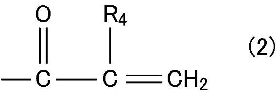
(式(2)中、R4は、水素原子又はアルキル基を示す)
並びに、前記表面処理銅箔が、銅箔の少なくとも一方の面側に銅の微細粗化粒子処理層を有する表面処理銅箔であって、前記微細粗化粒子処理層が粒子径40~200nmの微細銅粒子で構成されており、前記微細粗化粒子処理層上にニッケルを含む耐熱処理層を有し、前記耐熱処理層上に少なくともクロムを含む防錆処理層を有し、前記防錆処理層上にシランカップリング剤層を有し、かつ、前記耐熱処理層中のニッケル付着量が30~60mg/m2であることを特徴とする。
並びに、前記表面処理銅箔が、銅箔の少なくとも一方の面側に銅の微細粗化粒子処理層を有する表面処理銅箔であって、前記微細粗化粒子処理層が粒子径40~200nmの微細銅粒子で構成されており、前記微細粗化粒子処理層上にニッケルを含む耐熱処理層を有し、前記耐熱処理層上に少なくともクロムを含む防錆処理層を有し、前記防錆処理層上にシランカップリング剤層を有し、かつ、前記耐熱処理層中のニッケル付着量が30~60mg/m2であることを特徴とする。
このような構成により、高速信号伝送基板の伝送損失を低減させることができ、かつ、密着性と耐熱性に優れる銅張積層板を提供することができる。
前記銅張積層板において、前記化合物が前記式(1)または(2)で表される基で末端変性された、変性ポリフェニレンエーテル化合物を含むことが好ましい。それにより、さらに優れた低誘電特性を得ることができる。また、前記変性ポリフェニレンエーテル化合物の重量平均分子量(Mw)が500~5000であることが好ましい。それにより、上記効果をより確実に得ることができると考えられる。
さらに、前記銅張積層板において、絶縁層の樹脂組成物に含まれる前記化合物の含有量が、化合物と架橋型硬化剤との合計100質量部に対して、30~95質量部であることが好ましい。それにより、上記効果をより確実に得ることができると考えられる。
また、前記銅張積層板において、前記架橋型硬化剤が、トリアルケニルイソシアヌレート化合物、分子中にアクリル基を2個以上有する多官能アクリレート化合物、分子中にメタクリル基を2個以上有する多官能メタクリレート化合物、分子中にビニル基を2個以上有する多官能ビニル化合物、分子中にアリル基を有するアリル化合物、分子中にマレイミド基を有するマレイミド系化合物及びアセナフチレン化合物からなる群から選ばれる少なくとも1種を含むことが好ましい。これにより、耐熱性をより高めることができる。
また、前記ポリフェニレンエーテル化合物は、2,6-ジメチルフェノールと2官能フェノール由来の構造を含むことが好ましく、さらに、前記式(1)で表される基が、p-エテニルベンジル基及びm-エテニルベンジル基からなる群から選ばれる少なくとも1種を含むことが好ましい。
また、前記表面処理銅箔において、前記耐熱処理層がニッケルまたはニッケルとリンとで構成されていることが好ましい。それにより、上述したような効果をより確実に得ることができる。
本発明のさらなる態様に係る樹脂付銅箔は、上述したような樹脂組成物又は前記樹脂組成物の半硬化物を含む樹脂層と、前記樹脂層の片面に上述の表面処理銅箔とを備えることを特徴とする。
さらに、本発明には、上記銅張積層板または上記樹脂付銅箔を備え、その表面に回路としての導体パターンとを有する回路基板も包含される。
また、本発明には、樹脂組成物の硬化物からなる絶縁層と、前記絶縁層の片面又は両面に接する表面処理銅箔とを備える銅張積層板における前記絶縁層形成用の樹脂組成物であって、分子中に下記式(1)または(2)で表される基を少なくとも1つ有する化合物と架橋型硬化剤とを含むこと、

(式(1)中、sは0~10の整数を示す。また、Zは、アリーレン基を示す。また、R1~R3は、それぞれ独立して、水素原子又はアルキル基を示す)

(式(2)中、R4は、水素原子又はアルキル基を示す)
並びに、
前記表面処理銅箔が、銅箔の少なくとも一方の面側に銅の微細粗化粒子処理層を有する表面処理銅箔であって、前記微細粗化粒子処理層が粒子径40~200nmの微細銅粒子で構成されており、前記微細粗化粒子処理層上にニッケルを含む耐熱処理層を有し、
前記耐熱処理層上に少なくともクロムを含む防錆処理層を有し、前記防錆処理層上にシランカップリング剤層を有し、かつ、前記耐熱処理層中のニッケル付着量が30~60mg/m2であることを特徴とする樹脂組成物をも包含される。
並びに、
前記表面処理銅箔が、銅箔の少なくとも一方の面側に銅の微細粗化粒子処理層を有する表面処理銅箔であって、前記微細粗化粒子処理層が粒子径40~200nmの微細銅粒子で構成されており、前記微細粗化粒子処理層上にニッケルを含む耐熱処理層を有し、
前記耐熱処理層上に少なくともクロムを含む防錆処理層を有し、前記防錆処理層上にシランカップリング剤層を有し、かつ、前記耐熱処理層中のニッケル付着量が30~60mg/m2であることを特徴とする樹脂組成物をも包含される。
以下に、実施例により本発明を更に具体的に説明するが、本発明の範囲はこれらに限定されるものではない。
まず、本実施例において、樹脂組成物を調製する際に用いる各成分について説明する。
・変性PPE1
ポリフェニレンエーテルと、クロロメチルスチレンとを反応させて変性ポリフェニレンエーテル1(変性PPE1)を得た。
ポリフェニレンエーテルと、クロロメチルスチレンとを反応させて変性ポリフェニレンエーテル1(変性PPE1)を得た。
具体的には、まず、温度調節器、攪拌装置、冷却設備、及び滴下ロートを備えた1リットルの3つ口フラスコに、ポリフェニレンエーテル(ポリフェニレンエーテル、SABICイノベーティブプラスチックス社製のSA90、末端水酸基数2個、重量平均分子量Mw1700)200g、p-クロロメチルスチレンとm-クロロメチルスチレンとの質量比が50:50の混合物(東京化成工業株式会社製のクロロメチルスチレン:CMS)30g、相間移動触媒として、テトラ-n-ブチルアンモニウムブロマイド1.227g、及びトルエン400gを仕込み、攪拌した。そして、ポリフェニレンエーテル、クロロメチルスチレン、及びテトラ-n-ブチルアンモニウムブロマイドが、トルエンに溶解するまで攪拌した。その際、徐々に加熱し、最終的に液温が75℃になるまで加熱した。そして、その溶液に、アルカリ金属水酸化物として、水酸化ナトリウム水溶液(水酸化ナトリウム20g/水20g)を20分間かけて、滴下した。その後、さらに、75℃で4時間攪拌した。次に、10質量%の塩酸でフラスコの内容物を中和した後、多量のメタノールを投入した。そうすることによって、フラスコ内の液体に沈殿物を生じさせた。すなわち、フラスコ内の反応液に含まれる生成物を再沈させた。そして、この沈殿物をろ過によって取り出し、メタノールと水との質量比が80:20の混合液で3回洗浄した後、減圧下、80℃で3時間乾燥させた。そして、重量平均分子量(Mw)2300の末端ビニルベンゼン変性PPE(変性PPE1)を得た。
得られた固体を、1H-NMR(400MHz、CDCl3、TMS)で分析した。NMRを測定した結果、5~7ppmにエテニルベンジルに由来するピークが確認された。これにより、得られた固体が、エテニルベンジル化されたポリフェニレンエーテルであることが確認できた。
・変性PPE2
ポリフェニレンエーテルとして、後述するポリフェニレンエーテルを用い、後述の条件にしたこと以外、変性PPE1の合成と同様の方法で合成した。
ポリフェニレンエーテルとして、後述するポリフェニレンエーテルを用い、後述の条件にしたこと以外、変性PPE1の合成と同様の方法で合成した。
用いたポリフェニレンエーテルは、SABICイノベーティブプラスチックス社製のSA120(固有粘度(IV)0.125dl/g、末端水酸基数1個、重量平均分子量Mw3100)であった。
次に、ポリフェニレンエーテルと、クロロメチルスチレンとの反応は、前記ポリフェニレンエーテル(SA120)を200g、CMSを15g、相間移動触媒(テトラ-n-ブチルアンモニウムブロマイド)を0.92g用い、水酸化ナトリウム水溶液(水酸化ナトリウム20g/水20g)の代わりに、水酸化ナトリウム水溶液(水酸化ナトリウム10g/水10g)を用いたこと以外、変性PPE1の合成と同様の方法で合成することによって、重量平均分子量(Mw)3300の末端ビニルベンゼン変性PPE(変性PPE2)を得た。
そして、得られた固体を、1H-NMR(400MHz、CDCl3、TMS)で分析した。NMRを測定した結果、5~7ppmにエテニルベンジルに由来するピークが確認された。これにより、得られた固体が、エテニルベンジル化されたポリフェニレンエーテルであることが確認できた。
・SA9000:SABICイノベーティブプラスチックス社製のSA9000(末端メタクリル基変性PPE、重量平均分子量(Mw)2000)
・SA90:SABICイノベーティブプラスチックス社製のSA90(未変性PPE、重量平均分子量(Mw)1700)
・架橋型硬化剤:TAIC(トリアリルイソシアヌレート、日本化成株式会社製)
・反応開始剤:パーブチルP:1,3-ジ(t-ブチルパーオキシイソプロピル)ベンゼン(日油株式会社製のパーブチルP)
・SA90:SABICイノベーティブプラスチックス社製のSA90(未変性PPE、重量平均分子量(Mw)1700)
・架橋型硬化剤:TAIC(トリアリルイソシアヌレート、日本化成株式会社製)
・反応開始剤:パーブチルP:1,3-ジ(t-ブチルパーオキシイソプロピル)ベンゼン(日油株式会社製のパーブチルP)
<表面処理銅箔の作成>
(表面処理銅箔1)
前処理として、100g/L硫酸水溶液中で陰極に銅板、陽極に上記未処理銅箔を使用し電流密度5A/dm2で6秒間電解を行い、未処理銅箔表面の酸化層除去及び活性化を行った。
(表面処理銅箔1)
前処理として、100g/L硫酸水溶液中で陰極に銅板、陽極に上記未処理銅箔を使用し電流密度5A/dm2で6秒間電解を行い、未処理銅箔表面の酸化層除去及び活性化を行った。
次いで、以下に示す浴組成、電解条件で処理することで、該未処理銅箔のラミネート面側に銅の微細粗化粒子処理層を形成させた。
(浴組成)
硫酸銅五水和物 35g/L
ジエチレントリアミン五酢酸五ナトリウム 100g/L
pH4.8
(電解条件)
電流密度:6A/dm2
電気量:50A・sec/dm2
液温:30℃
電極:銅板。
硫酸銅五水和物 35g/L
ジエチレントリアミン五酢酸五ナトリウム 100g/L
pH4.8
(電解条件)
電流密度:6A/dm2
電気量:50A・sec/dm2
液温:30℃
電極:銅板。
得られた微細粗化粒子処理層を、電界放射型走査電子顕微鏡FE-SEM(日本電子製JSM-7800F)を使用し、試料台を40°傾斜させながら倍率80,000倍で観察した。その結果観察された銅粒子の高さを粒子径の値として、前記微細粗化粒子処理層における粗化粒子の粒子径は、最小値40nm、最大値200nmであった。
次いで、水洗後、二層目表面処理層である耐熱処理層を、以下に示す浴組成、電解条件で処理することで形成させた。
(浴組成)
硫酸ニッケル六水和物 30g/L
酢酸ナトリウム三水和物 10g/L
次亜リン酸ナトリウム一水和物 2.0g/L
(電解条件)
電流密度:1.6A/dm2
電気量:2.7A・sec/dm2
pH4.5
液温:32℃
陽極:白金族酸化物被覆チタン板。
硫酸ニッケル六水和物 30g/L
酢酸ナトリウム三水和物 10g/L
次亜リン酸ナトリウム一水和物 2.0g/L
(電解条件)
電流密度:1.6A/dm2
電気量:2.7A・sec/dm2
pH4.5
液温:32℃
陽極:白金族酸化物被覆チタン板。
得られた耐熱処理層におけるニッケル付着量は、被処理銅箔を硝酸で溶解、希釈してICP発光分光分析装置によりニッケルの濃度を分析することによって測定した。その結果、ニッケル付着量は56mg/m2であった。
次いで、水洗後、三層目表面処理層となる防錆処理層を、以下に示す電解浴組成、pH、電解条件で処理を施した。
(浴組成)
重クロム酸ナトリウム:10g/L
亜鉛イオン:1.0g/L
水酸化ナトリウム:40g/L
液温:30℃
(電解条件)
電流密度:4A/dm2
電気量:5.5A・sec/dm2
陽極:白金族酸化物被覆チタン板。
重クロム酸ナトリウム:10g/L
亜鉛イオン:1.0g/L
水酸化ナトリウム:40g/L
液温:30℃
(電解条件)
電流密度:4A/dm2
電気量:5.5A・sec/dm2
陽極:白金族酸化物被覆チタン板。
次いで、水洗後、四層目表面処理層となるシランカップリング剤処理層を、以下に示す浴組成、液温、浸漬時間で処理を施すことにより形成し、実施例1の表面処理銅箔を得た。
(浴組成)
γ-アミノプロピルトリエトキシシラン 2mL/L
液温:30℃
浸漬時間:15秒。
γ-アミノプロピルトリエトキシシラン 2mL/L
液温:30℃
浸漬時間:15秒。
(表面処理銅箔2)
二層目の耐熱処理層を、以下に示す浴組成、電解条件で処理することで形成させた以外は、表面処理銅箔1と同様にして、表面処理銅箔2を得た。得られた耐熱処理層におけるニッケル付着量は32mg/m2であった。
二層目の耐熱処理層を、以下に示す浴組成、電解条件で処理することで形成させた以外は、表面処理銅箔1と同様にして、表面処理銅箔2を得た。得られた耐熱処理層におけるニッケル付着量は32mg/m2であった。
(浴組成)
硫酸ニッケル六水和物 30g/L
酢酸ナトリウム三水和物 10g/L
次亜リン酸ナトリウム一水和物 2.0g/L
pH4.5
(電解条件)
電流密度:1.0A/dm2
電気量:1.8A・sec/dm2
液温:32℃
電極:白金族酸化物被覆チタン板。
硫酸ニッケル六水和物 30g/L
酢酸ナトリウム三水和物 10g/L
次亜リン酸ナトリウム一水和物 2.0g/L
pH4.5
(電解条件)
電流密度:1.0A/dm2
電気量:1.8A・sec/dm2
液温:32℃
電極:白金族酸化物被覆チタン板。
(表面処理銅箔3)
二層目の耐熱処理層を設けなかったこと以外は、表面処理銅箔1と同様にして、表面処理銅箔3を得た。得られた表面処理銅箔3におけるニッケル付着量は0mg/m2であった。
二層目の耐熱処理層を設けなかったこと以外は、表面処理銅箔1と同様にして、表面処理銅箔3を得た。得られた表面処理銅箔3におけるニッケル付着量は0mg/m2であった。
(表面処理銅箔4)
二層目の耐熱処理層を、以下に示す浴組成、電解条件で処理することで形成させた以外は、表面処理銅箔1と同様にして、表面処理銅箔4を得た。得られた耐熱処理層におけるニッケル付着量は82mg/m2であった。
二層目の耐熱処理層を、以下に示す浴組成、電解条件で処理することで形成させた以外は、表面処理銅箔1と同様にして、表面処理銅箔4を得た。得られた耐熱処理層におけるニッケル付着量は82mg/m2であった。
(浴組成)
硫酸ニッケル六水和物 30g/L
酢酸ナトリウム三水和物 10g/L
次亜リン酸ナトリウム一水和物 2.0g/L
(電解条件)
電流密度:2.1A/dm2
電気量:3.6A・sec/dm2
pH4.5
液温:32℃
陽極:白金族酸化物被覆チタン板。
硫酸ニッケル六水和物 30g/L
酢酸ナトリウム三水和物 10g/L
次亜リン酸ナトリウム一水和物 2.0g/L
(電解条件)
電流密度:2.1A/dm2
電気量:3.6A・sec/dm2
pH4.5
液温:32℃
陽極:白金族酸化物被覆チタン板。
(表面処理銅箔5)
福田金属箔粉工業株式会社製「T4X-SV」を、表面処理銅箔5として使用した。この表面処理銅箔の耐熱処理層におけるニッケル付着量は106mg/m2であった。
福田金属箔粉工業株式会社製「T4X-SV」を、表面処理銅箔5として使用した。この表面処理銅箔の耐熱処理層におけるニッケル付着量は106mg/m2であった。
(表面処理銅箔6)
一層目の微細粗化粒子処理層を、以下に示す浴組成、電解条件で処理することで形成させた以外は、表面処理銅箔1と同様にして、表面処理銅箔6を得た。得られた微細粗化粒子処理層における粗化粒子の粒子径は、最小値700nm、最大値1400nmであった。また、得られた耐熱処理層におけるニッケル付着量は32mg/m2であった。
一層目の微細粗化粒子処理層を、以下に示す浴組成、電解条件で処理することで形成させた以外は、表面処理銅箔1と同様にして、表面処理銅箔6を得た。得られた微細粗化粒子処理層における粗化粒子の粒子径は、最小値700nm、最大値1400nmであった。また、得られた耐熱処理層におけるニッケル付着量は32mg/m2であった。
(浴組成)
浴(1) 硫酸銅五水和物 47g/L
硫酸100g/L
浴(2) 硫酸銅五水和物 200g/L
硫酸100g/L。
浴(1) 硫酸銅五水和物 47g/L
硫酸100g/L
浴(2) 硫酸銅五水和物 200g/L
硫酸100g/L。
(電解条件)
浴(1)にて電流密度50A/dm2、電気量130A・sec/dm2、液温30℃の電解条件にて電解して微細銅粒子を付着させた後、さらに浴(2)にて電流密度5A/dm2、電気量400A・sec/dm2、液温40℃の電解条件にて電解することで微細粗化粒子処理層を形成した。
浴(1)にて電流密度50A/dm2、電気量130A・sec/dm2、液温30℃の電解条件にて電解して微細銅粒子を付着させた後、さらに浴(2)にて電流密度5A/dm2、電気量400A・sec/dm2、液温40℃の電解条件にて電解することで微細粗化粒子処理層を形成した。
(表面処理銅箔7)
二層目の耐熱処理層を、以下に示す浴組成、電解条件で処理することで形成させ、さらに防錆処理層を形成しなかったこと以外は、表面処理銅箔1と同様にして、表面処理銅箔7を得た。得られた耐熱処理層におけるニッケル付着量は42mg/m2であった。
二層目の耐熱処理層を、以下に示す浴組成、電解条件で処理することで形成させ、さらに防錆処理層を形成しなかったこと以外は、表面処理銅箔1と同様にして、表面処理銅箔7を得た。得られた耐熱処理層におけるニッケル付着量は42mg/m2であった。
(浴組成)
硫酸ニッケル六水和物 30g/L
酢酸ナトリウム三水和物 10g/L
次亜リン酸ナトリウム一水和物 2.0g/L
(電解条件)
電流密度:1.3A/dm2
電気量:2.3A・sec/dm2
pH4.5
液温:32℃
陽極:白金族酸化物被覆チタン板。
硫酸ニッケル六水和物 30g/L
酢酸ナトリウム三水和物 10g/L
次亜リン酸ナトリウム一水和物 2.0g/L
(電解条件)
電流密度:1.3A/dm2
電気量:2.3A・sec/dm2
pH4.5
液温:32℃
陽極:白金族酸化物被覆チタン板。
<実施例1~6および比較例1~6の銅張積層板の作成>
まず、開始剤以外の樹脂組成物の各成分を表1に記載の配合割合(表中の配合割合は質量部で示す)で、固形分濃度が60質量%となるように、トルエンに添加し、混合させた。その混合物を、80℃になるまで加熱し、80℃のままで30分間攪拌した。その後、その攪拌した混合物を40℃まで冷却した後、開始剤である1,3-ビス(ブチルパーオキシイソプロピル)ベンゼン(日油株式会社製のパーブチルP)を表1に記載の配合割合で添加することによって、各実施例および比較例のワニス状の樹脂組成物(樹脂ワニス)を得た。この樹脂ワニスを使用して、以下の評価用基板を作製した。
まず、開始剤以外の樹脂組成物の各成分を表1に記載の配合割合(表中の配合割合は質量部で示す)で、固形分濃度が60質量%となるように、トルエンに添加し、混合させた。その混合物を、80℃になるまで加熱し、80℃のままで30分間攪拌した。その後、その攪拌した混合物を40℃まで冷却した後、開始剤である1,3-ビス(ブチルパーオキシイソプロピル)ベンゼン(日油株式会社製のパーブチルP)を表1に記載の配合割合で添加することによって、各実施例および比較例のワニス状の樹脂組成物(樹脂ワニス)を得た。この樹脂ワニスを使用して、以下の評価用基板を作製した。
(耐熱性評価用基板)
実施例および各比較例1~3で得られた樹脂ワニスをそれぞれガラス基材(♯2116タイプ、「Lガラス」(旭化成株式会社製、比誘電率4.6)に含浸させた後、130℃で約3~8分間加熱乾燥することによりプリプレグを得た。その際、ポリフェニレンエーテル、及び架橋剤等の樹脂成分の含有量(レジンコンテント)が約50質量%となるように調整した。
実施例および各比較例1~3で得られた樹脂ワニスをそれぞれガラス基材(♯2116タイプ、「Lガラス」(旭化成株式会社製、比誘電率4.6)に含浸させた後、130℃で約3~8分間加熱乾燥することによりプリプレグを得た。その際、ポリフェニレンエーテル、及び架橋剤等の樹脂成分の含有量(レジンコンテント)が約50質量%となるように調整した。
そして、得られた各プリプレグを6枚重ねて積層し、それぞれ表1に示す銅箔を両面に重ねて、温度200℃、2時間、圧力3MPaの条件で加熱加圧することにより、750μmの厚みの評価用銅張積層板を得た。
(伝送特性評価用基板)
実施例および各比較例1~3で得られた樹脂ワニスをそれぞれガラス基材(♯1078タイプ、「Lガラス」(旭化成株式会社製、比誘電率4.6)に含浸させた後、130℃で約3~8分間加熱乾燥することによりプリプレグを得た。その際、ポリフェニレンエーテル、及び架橋剤等の樹脂成分の含有量(レジンコンテント)が約60質量%となるように調整した。
実施例および各比較例1~3で得られた樹脂ワニスをそれぞれガラス基材(♯1078タイプ、「Lガラス」(旭化成株式会社製、比誘電率4.6)に含浸させた後、130℃で約3~8分間加熱乾燥することによりプリプレグを得た。その際、ポリフェニレンエーテル、及び架橋剤等の樹脂成分の含有量(レジンコンテント)が約60質量%となるように調整した。
そして、得られた各プリプレグを2枚重ねて積層し、それぞれ表1に示す銅箔を両面に重ねて、温度200℃、2時間、圧力3MPaの条件で加熱加圧することにより、150μmの厚みの評価用銅張積層板を得た。
次に、得られた両面板の片面を線幅100~200μmで加工した後、加工面を挟むようにさらにプリプレグ2枚を2次積層し、3層板を作製した。線幅は仕上がり後、回路の特性インピーダンスが50Ωとなるように調整した。
得られた積層板について、伝送特性はネットワークアナライザー(キーサイトテクノロジー社製 N5230A)を用いて通過損失を評価した。なお、評価周波数は20GHzであった。
[オーブン耐熱試験]
得られた銅箔張積層板を用いて、JIS C 6481に準じて作製した試験片を、250℃、260℃、280℃、及び300℃に設定した空気循環装置付き恒温槽中で一時間処理したときに、試験片5枚中全て異常がなかったものを「○」、試験片5枚中1枚以上のサンプルにおいて「ふくれ」又は「はがれ」が生じたものを「×」と判定した。本試験においては、280℃で「○」の評価を得たサンプルを合格とする。
得られた銅箔張積層板を用いて、JIS C 6481に準じて作製した試験片を、250℃、260℃、280℃、及び300℃に設定した空気循環装置付き恒温槽中で一時間処理したときに、試験片5枚中全て異常がなかったものを「○」、試験片5枚中1枚以上のサンプルにおいて「ふくれ」又は「はがれ」が生じたものを「×」と判定した。本試験においては、280℃で「○」の評価を得たサンプルを合格とする。
以上の試験結果を表1に示す。
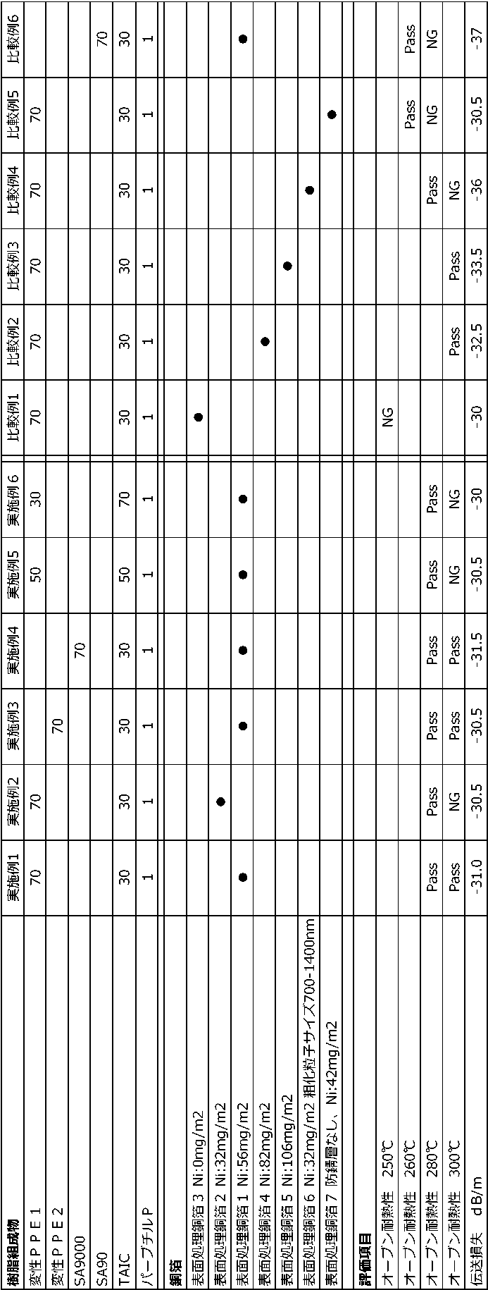
表1の結果から明らかなように、本発明の表面処理銅箔および樹脂組成物を用いた積層板では、優れた耐熱性を有し、かつ、伝送特性にも優れていることが確認された。
これに対し、表面処理銅箔の耐熱処理層におけるニッケル付着量が0であった比較例1では、耐熱性を得ることができなかった。一方で、耐熱処理層におけるニッケル付着量が過剰となっていた比較例2および比較例3では、伝送特性は不十分であった。
また、微細粗化粒子処理層における銅粒子サイズが大きかった比較例4では、伝送特性に劣り、耐熱性も十分とは言い難い結果となった。防錆処理層を形成しなかった比較例5でも十分な耐熱性を得ることはできなかった。
そして、式(1)または式(2)で表される基を有さない化合物を使用した比較例6では、耐熱性も伝送特性も得ることができなかった。
この出願は、2019年2月4日に出願された日本国特許出願特願2019-018130を基礎とするものであり、その内容は、本願に含まれるものである。
本発明を表現するために、前述において具体例や図面等を参照しながら実施形態を通して本発明を適切かつ十分に説明したが、当業者であれば前述の実施形態を変更及び/又は改良することは容易になし得ることであると認識すべきである。したがって、当業者が実施する変更形態又は改良形態が、請求の範囲に記載された請求項の権利範囲を離脱するレベルのものでない限り、当該変更形態又は当該改良形態は、当該請求項の権利範囲に包括されると解釈される。
本発明は、伝送基板(回路基板)用の電子材料やそれを用いた各種デバイスに関する技術分野において、広範な産業上の利用可能性を有する。
Claims (11)
- 樹脂組成物の硬化物からなる絶縁層と、前記絶縁層の片面又は両面に接する表面処理銅箔とを備える銅張積層板であって、
前記樹脂組成物が、分子中に下記式(1)または(2)で表される基を少なくとも1つ有する化合物と架橋型硬化剤とを含むこと、

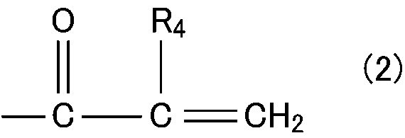
並びに、
前記表面処理銅箔が、銅箔の少なくとも一方の面側に銅の微細粗化粒子処理層を有する表面処理銅箔であって、
前記微細粗化粒子処理層が粒子径40~200nmの微細銅粒子で構成されており、
前記微細粗化粒子処理層上にニッケルを含む耐熱処理層を有し、
前記耐熱処理層上に少なくともクロムを含む防錆処理層を有し、
前記防錆処理層上にシランカップリング剤処理層を有し、かつ、
前記耐熱処理層中のニッケル付着量が30~60mg/m2であることを特徴とする、
銅張積層板。 - 前記化合物が、前記式(1)または式(2)で末端を変性された、変性ポリフェニレンエーテル化合物を含む、請求項1に記載の銅張積層板。
- 前記化合物の重量平均分子量(Mw)が500~5000である、請求項2に記載の銅張積層板。
- 前記化合物の含有量が、化合物と架橋型硬化剤との合計100質量部に対して、30~95質量部である、請求項1~3のいずれかに記載の銅張積層板。
- 前記架橋型硬化剤が、トリアルケニルイソシアヌレート化合物、分子中にアクリル基を2個以上有する多官能アクリレート化合物、分子中にメタクリル基を2個以上有する多官能メタクリレート化合物、分子中にビニル基を2個以上有する多官能ビニル化合物、スチレン誘導体、分子中にアリル基を有するアリル化合物、分子中にマレイミド基を有するマレイミド系化合物及びアセナフチレン化合物からなる群から選ばれる少なくとも1種を含む、請求項1~4のいずれかに記載の銅張積層板。
- 前記ポリフェニレンエーテル共重合体は、2,6-ジメチルフェノールと2官能フェノール由来の構造を含む、請求項1~5のいずれかに記載の銅張積層板。
- 前記式(1)で表される基が、p-エテニルベンジル基及びm-エテニルベンジル基からなる群から選ばれる少なくとも1種を含む、請求項1~6のいずれかに記載の銅張積層板。
- 前記表面処理銅箔において前記耐熱処理層がニッケルまたはニッケルとリンとで構成されている、請求項1~7のいずれかに記載の銅張積層板。
- 樹脂組成物又は前記樹脂組成物の半硬化物を含む樹脂層と、前記樹脂層の片面に接する表面処理銅箔とを備える樹脂付銅箔であって、
前記樹脂組成物が、分子中に下記式(1)または(2)で表される基を少なくとも1つ有する化合物と架橋型硬化剤とを含むこと、
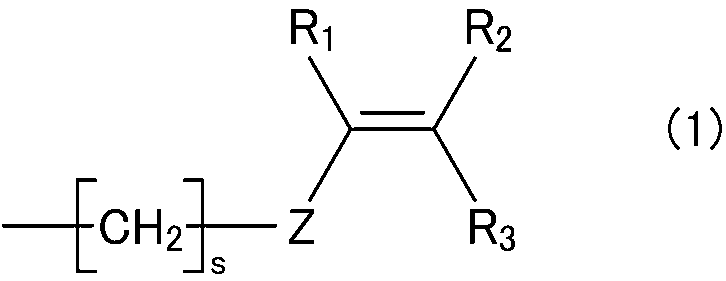

並びに、
前記表面処理銅箔が、銅箔の少なくとも一方の面側に銅の微細粗化粒子処理層を有する表面処理銅箔であって、
前記微細粗化粒子処理層が粒子径40~200nmの微細銅粒子で構成されており、
前記微細粗化粒子処理層上にニッケルを含む耐熱処理層を有し、
前記耐熱処理層上に少なくともクロムを含む防錆処理層を有し、
前記防錆処理層上にシランカップリング剤層を有し、かつ、
前記耐熱処理層中のニッケル付着量が30~60mg/m2であることを特徴とする、
樹脂付銅箔。 - 請求項1~8のいずれかに記載の銅張積層板または請求項9に記載の樹脂付銅箔を備え、その表面に回路としての導体パターンとを有する、回路基板。
- 樹脂組成物の硬化物からなる絶縁層と、前記絶縁層の片面又は両面に接する表面処理銅箔とを備える銅張積層板における前記絶縁層形成用の樹脂組成物であって、
分子中に下記式(1)または(2)で表される基を少なくとも1つ有する化合物と架橋型硬化剤とを含むこと、
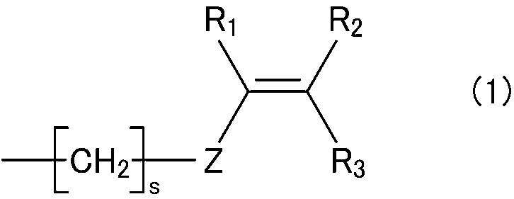

並びに、
前記表面処理銅箔が、銅箔の少なくとも一方の面側に銅の微細粗化粒子処理層を有する表面処理銅箔であって、
前記微細粗化粒子処理層が粒子径40~200nmの微細銅粒子で構成されており、
前記微細粗化粒子処理層上にニッケルを含む耐熱処理層を有し、
前記耐熱処理層上に少なくともクロムを含む防錆処理層を有し、
前記防錆処理層上にシランカップリング剤層を有し、かつ、
前記耐熱処理層中のニッケル付着量が30~60mg/m2であることを特徴とする樹脂組成物。
Priority Applications (3)
| Application Number | Priority Date | Filing Date | Title |
|---|---|---|---|
| US17/426,400 US11866536B2 (en) | 2019-02-04 | 2019-12-18 | Copper-clad laminate plate, resin-attached copper foil, and circuit board using same |
| JP2020571031A JP7325022B2 (ja) | 2019-02-04 | 2019-12-18 | 銅張積層板、樹脂付銅箔、および、それらを用いた回路基板 |
| CN201980090624.8A CN113543973A (zh) | 2019-02-04 | 2019-12-18 | 覆铜箔层压板、带树脂的铜箔以及使用它们的电路板 |
Applications Claiming Priority (2)
| Application Number | Priority Date | Filing Date | Title |
|---|---|---|---|
| JP2019-018130 | 2019-02-04 | ||
| JP2019018130 | 2019-02-04 |
Publications (1)
| Publication Number | Publication Date |
|---|---|
| WO2020162056A1 true WO2020162056A1 (ja) | 2020-08-13 |
Family
ID=71947813
Family Applications (1)
| Application Number | Title | Priority Date | Filing Date |
|---|---|---|---|
| PCT/JP2019/049693 Ceased WO2020162056A1 (ja) | 2019-02-04 | 2019-12-18 | 銅張積層板、樹脂付銅箔、および、それらを用いた回路基板 |
Country Status (4)
| Country | Link |
|---|---|
| US (1) | US11866536B2 (ja) |
| JP (1) | JP7325022B2 (ja) |
| CN (1) | CN113543973A (ja) |
| WO (1) | WO2020162056A1 (ja) |
Cited By (3)
| Publication number | Priority date | Publication date | Assignee | Title |
|---|---|---|---|---|
| CN116762482A (zh) * | 2021-03-11 | 2023-09-15 | 乐天能源材料公司 | 具有低表面粗糙度及低翘曲的表面处理铜箔、包括该铜箔的铜箔基板及包括该铜箔的印刷配线板 |
| WO2024034276A1 (ja) | 2022-08-09 | 2024-02-15 | 三菱瓦斯化学株式会社 | 金属箔張積層板の製造方法、樹脂組成物、樹脂複合シート、プリント配線板の製造方法、および、半導体装置の製造方法 |
| US20240215172A1 (en) * | 2021-04-09 | 2024-06-27 | Fukuda Metal Foil & Powder Co., Ltd. | Surface-treated copper foil, copper-clad laminate and printed wiring board using the surface-treated copper foil |
Families Citing this family (4)
| Publication number | Priority date | Publication date | Assignee | Title |
|---|---|---|---|---|
| US11770904B2 (en) * | 2019-02-04 | 2023-09-26 | Panasonic Intellectual Property Management Co., Ltd. | Surface-treated copper foil, and copper-clad laminate plate, resin-attached copper foil and circuit board each using same |
| CN114503789B (zh) * | 2019-10-25 | 2025-05-16 | 纳美仕有限公司 | 复合铜部件 |
| US12342449B2 (en) * | 2021-09-28 | 2025-06-24 | The Board Of Trustees Of The University Of Illinois | Multilayered nonpolar, chromium, copper material coatings of power electronics boards for thermal management |
| CN119040979B (zh) * | 2024-08-23 | 2025-06-24 | 浙江花园新能源股份有限公司 | 一种铜箔的表面处理工艺及其产品和应用 |
Citations (5)
| Publication number | Priority date | Publication date | Assignee | Title |
|---|---|---|---|---|
| JP2016028885A (ja) * | 2014-07-16 | 2016-03-03 | パナソニックIpマネジメント株式会社 | 金属張積層板とその製造方法、樹脂付き金属箔、及びプリント配線板 |
| WO2016174998A1 (ja) * | 2015-04-28 | 2016-11-03 | 三井金属鉱業株式会社 | 粗化処理銅箔及びプリント配線板 |
| WO2017026500A1 (ja) * | 2015-08-12 | 2017-02-16 | 古河電気工業株式会社 | 表面処理銅箔及びこれを用いて製造される銅張積層板又はプリント配線板 |
| JP2018090906A (ja) * | 2016-12-06 | 2018-06-14 | Jx金属株式会社 | 表面処理銅箔、キャリア付銅箔、積層体、プリント配線板の製造方法及び電子機器の製造方法 |
| JP2019001965A (ja) * | 2017-06-19 | 2019-01-10 | パナソニックIpマネジメント株式会社 | 樹脂組成物、プリプレグ、金属張積層板及びプリント配線板 |
Family Cites Families (6)
| Publication number | Priority date | Publication date | Assignee | Title |
|---|---|---|---|---|
| JP6110581B2 (ja) | 2014-12-05 | 2017-04-05 | 三井金属鉱業株式会社 | 高周波信号伝送回路形成用表面処理銅箔、銅張積層板及びプリント配線板 |
| WO2017033784A1 (ja) * | 2015-08-25 | 2017-03-02 | 三井金属鉱業株式会社 | 樹脂層付金属箔、金属張積層板、及びプリント配線板の製造方法 |
| JP6182584B2 (ja) | 2015-12-09 | 2017-08-16 | 古河電気工業株式会社 | プリント配線板用表面処理銅箔、プリント配線板用銅張積層板及びプリント配線板 |
| JP6601675B2 (ja) * | 2016-01-14 | 2019-11-06 | パナソニックIpマネジメント株式会社 | 金属張積層板および樹脂付金属箔 |
| KR102766324B1 (ko) * | 2018-10-05 | 2025-02-10 | 파나소닉 아이피 매니지먼트 가부시키가이샤 | 구리 클래드 적층판, 배선판, 및 수지 부착 구리박 |
| CN114555360A (zh) * | 2019-10-25 | 2022-05-27 | 松下知识产权经营株式会社 | 覆铜箔层压板、布线板、以及带树脂的铜箔 |
-
2019
- 2019-12-18 US US17/426,400 patent/US11866536B2/en active Active
- 2019-12-18 JP JP2020571031A patent/JP7325022B2/ja active Active
- 2019-12-18 WO PCT/JP2019/049693 patent/WO2020162056A1/ja not_active Ceased
- 2019-12-18 CN CN201980090624.8A patent/CN113543973A/zh active Pending
Patent Citations (5)
| Publication number | Priority date | Publication date | Assignee | Title |
|---|---|---|---|---|
| JP2016028885A (ja) * | 2014-07-16 | 2016-03-03 | パナソニックIpマネジメント株式会社 | 金属張積層板とその製造方法、樹脂付き金属箔、及びプリント配線板 |
| WO2016174998A1 (ja) * | 2015-04-28 | 2016-11-03 | 三井金属鉱業株式会社 | 粗化処理銅箔及びプリント配線板 |
| WO2017026500A1 (ja) * | 2015-08-12 | 2017-02-16 | 古河電気工業株式会社 | 表面処理銅箔及びこれを用いて製造される銅張積層板又はプリント配線板 |
| JP2018090906A (ja) * | 2016-12-06 | 2018-06-14 | Jx金属株式会社 | 表面処理銅箔、キャリア付銅箔、積層体、プリント配線板の製造方法及び電子機器の製造方法 |
| JP2019001965A (ja) * | 2017-06-19 | 2019-01-10 | パナソニックIpマネジメント株式会社 | 樹脂組成物、プリプレグ、金属張積層板及びプリント配線板 |
Cited By (5)
| Publication number | Priority date | Publication date | Assignee | Title |
|---|---|---|---|---|
| CN116762482A (zh) * | 2021-03-11 | 2023-09-15 | 乐天能源材料公司 | 具有低表面粗糙度及低翘曲的表面处理铜箔、包括该铜箔的铜箔基板及包括该铜箔的印刷配线板 |
| EP4307846A4 (en) * | 2021-03-11 | 2025-03-19 | Lotte Energy Materials Corporation | Low-roughness surface-treated copper foil with low bending deformation, copper clad laminate comprising same, and printed wiring board |
| US20240215172A1 (en) * | 2021-04-09 | 2024-06-27 | Fukuda Metal Foil & Powder Co., Ltd. | Surface-treated copper foil, copper-clad laminate and printed wiring board using the surface-treated copper foil |
| US12063747B2 (en) * | 2021-04-09 | 2024-08-13 | Fukuda Metal Foil & Powder Co., Ltd. | Surface-treated copper foil, copper-clad laminate and printed wiring board using the surface-treated copper foil |
| WO2024034276A1 (ja) | 2022-08-09 | 2024-02-15 | 三菱瓦斯化学株式会社 | 金属箔張積層板の製造方法、樹脂組成物、樹脂複合シート、プリント配線板の製造方法、および、半導体装置の製造方法 |
Also Published As
| Publication number | Publication date |
|---|---|
| US11866536B2 (en) | 2024-01-09 |
| JP7325022B2 (ja) | 2023-08-14 |
| JPWO2020162056A1 (ja) | 2020-08-13 |
| CN113543973A (zh) | 2021-10-22 |
| US20220106426A1 (en) | 2022-04-07 |
Similar Documents
| Publication | Publication Date | Title |
|---|---|---|
| JP7325022B2 (ja) | 銅張積層板、樹脂付銅箔、および、それらを用いた回路基板 | |
| US12233621B2 (en) | Copper-clad laminated plate, resin-clad copper foil, and circuit substrate using said plate and foil | |
| JP7637902B2 (ja) | 銅張積層板、配線板、及び樹脂付き銅箔 | |
| JP7065463B2 (ja) | 金属張積層板、樹脂付き金属箔、及び配線板 | |
| JP7445830B2 (ja) | 銅張積層板、配線板、及び樹脂付き銅箔 | |
| JP7531109B2 (ja) | 金属張積層板、配線板、及び樹脂付き金属箔 | |
| KR20140102736A (ko) | 접착제층 부착 동박, 동박 적층판 및 프린트 배선판 | |
| KR20180035185A (ko) | 수지층 부착 금속박, 금속장 적층판, 및 프린트 배선판의 제조 방법 | |
| WO2017122249A1 (ja) | 金属張積層板および樹脂付金属箔 | |
| JP6967732B2 (ja) | 金属張積層板、樹脂付き金属部材、及び配線板 | |
| US10721823B2 (en) | Laminate production method | |
| JP7289074B2 (ja) | 樹脂組成物、並びに、それを用いたプリプレグ、樹脂付きフィルム、樹脂付き金属箔、金属張積層板及び配線基板 | |
| JP6994660B2 (ja) | 金属張積層板及びプリント配線板 | |
| JP7637901B2 (ja) | 金属張積層板、配線板、樹脂付き金属箔、及び樹脂組成物 | |
| JP7300613B2 (ja) | 樹脂組成物、並びに、それを用いたプリプレグ、樹脂付きフィルム、樹脂付き金属箔、金属張積層板及び配線基板 |
Legal Events
| Date | Code | Title | Description |
|---|---|---|---|
| 121 | Ep: the epo has been informed by wipo that ep was designated in this application |
Ref document number: 19914422 Country of ref document: EP Kind code of ref document: A1 |
|
| ENP | Entry into the national phase |
Ref document number: 2020571031 Country of ref document: JP Kind code of ref document: A |
|
| NENP | Non-entry into the national phase |
Ref country code: DE |
|
| 122 | Ep: pct application non-entry in european phase |
Ref document number: 19914422 Country of ref document: EP Kind code of ref document: A1 |