WO2020158810A1 - 平面アンテナ、平面アレイアンテナ、多軸アレイアンテナ、無線通信モジュールおよび無線通信装置 - Google Patents
平面アンテナ、平面アレイアンテナ、多軸アレイアンテナ、無線通信モジュールおよび無線通信装置 Download PDFInfo
- Publication number
- WO2020158810A1 WO2020158810A1 PCT/JP2020/003194 JP2020003194W WO2020158810A1 WO 2020158810 A1 WO2020158810 A1 WO 2020158810A1 JP 2020003194 W JP2020003194 W JP 2020003194W WO 2020158810 A1 WO2020158810 A1 WO 2020158810A1
- Authority
- WO
- WIPO (PCT)
- Prior art keywords
- planar
- conductor
- antenna
- axis
- ground conductor
- Prior art date
- Legal status (The legal status is an assumption and is not a legal conclusion. Google has not performed a legal analysis and makes no representation as to the accuracy of the status listed.)
- Ceased
Links
Images
Classifications
-
- H—ELECTRICITY
- H01—ELECTRIC ELEMENTS
- H01Q—ANTENNAS, i.e. RADIO AERIALS
- H01Q5/00—Arrangements for simultaneous operation of antennas on two or more different wavebands, e.g. dual-band or multi-band arrangements
- H01Q5/30—Arrangements for providing operation on different wavebands
- H01Q5/378—Combination of fed elements with parasitic elements
- H01Q5/385—Two or more parasitic elements
-
- H—ELECTRICITY
- H01—ELECTRIC ELEMENTS
- H01Q—ANTENNAS, i.e. RADIO AERIALS
- H01Q1/00—Details of, or arrangements associated with, antennas
- H01Q1/48—Earthing means; Earth screens; Counterpoises
-
- H—ELECTRICITY
- H01—ELECTRIC ELEMENTS
- H01Q—ANTENNAS, i.e. RADIO AERIALS
- H01Q21/00—Antenna arrays or systems
- H01Q21/06—Arrays of individually energised antenna units similarly polarised and spaced apart
- H01Q21/08—Arrays of individually energised antenna units similarly polarised and spaced apart the units being spaced along or adjacent to a rectilinear path
-
- H—ELECTRICITY
- H01—ELECTRIC ELEMENTS
- H01Q—ANTENNAS, i.e. RADIO AERIALS
- H01Q21/00—Antenna arrays or systems
- H01Q21/28—Combinations of substantially independent non-interacting antenna units or systems
-
- H—ELECTRICITY
- H01—ELECTRIC ELEMENTS
- H01Q—ANTENNAS, i.e. RADIO AERIALS
- H01Q9/00—Electrically-short antennas having dimensions not more than twice the operating wavelength and consisting of conductive active radiating elements
- H01Q9/04—Resonant antennas
- H01Q9/0407—Substantially flat resonant element parallel to ground plane, e.g. patch antenna
Definitions
- the present application relates to a planar antenna, a planar array antenna, a multi-axis array antenna, a wireless communication module and a wireless communication device.
- the communication speed required for wireless communication is also increasing, and high-frequency wireless communication technology capable of transmitting and receiving more information is required.
- the straightness of the electromagnetic wave increases, so that the communicable cell radius of the base station that transmits and receives radio waves to and from the wireless terminal decreases. Therefore, in wireless communication using a carrier wave of a short wavelength, base stations are generally arranged at a higher density than in the past.
- the number of base stations in close proximity to the wireless communication terminal will increase, and it is necessary to select a specific base station capable of high-quality communication from among a plurality of base stations in close proximity. May be. In other words, there is a case where an antenna having a wide radiable direction and high directivity is required.
- Patent Document 1 discloses a diversity antenna for receiving from a direction in which the strength of radio waves is strong.
- the present application provides a plane antenna, a plane array antenna, a multi-axis array antenna, a wireless communication module, and a wireless communication device capable of transmitting and receiving electromagnetic waves having high directivity in a short wavelength band.
- a planar antenna is located between a planar radiation conductor, a common ground conductor, the planar radiation conductor, and the common ground conductor, and has a first axis, a second axis, and a third axis.
- the first strip conductor extends in the extending direction.
- a second strip conductor extending in a direction orthogonal to the second strip conductor, which has an angle of 45 ⁇ 3° or ⁇ 45 ⁇ 3° with respect to the first axis and has a side facing the planar radiation conductor.
- a pair of parasitic conductors is located between a planar radiation conductor, a common ground conductor, the planar radiation conductor, and the common ground conductor, and has a first axis, a second axis, and a third axis.
- the planar antenna forms an angle of 45 ⁇ 3° with respect to the first axis, and has the pair of parasitic conductors having sides facing the planar radiation conductor, and the planar antenna with respect to the first axis.
- Another pair of parasitic conductors that form an angle of ⁇ 45 ⁇ 3° and that have a side facing the planar radiation conductor may be provided.
- planar radiation conductor and the parasitic conductor may be located on the same plane.
- the planar antenna further includes an antenna ground conductor located between the first strip conductor and the second strip conductor, and the common ground conductor, and the antenna ground conductor is at least the at least the third ground conductor when viewed from the third axial direction. It may overlap with the entire planar radiation conductor.
- the planar antenna may further include at least one first via conductor that connects the parasitic conductor and the antenna ground conductor.
- the planar antenna further includes a dielectric having a main surface perpendicular to the third axis direction, and the planar radiating conductor, the common ground conductor, the first strip conductor, the second strip conductor, and the parasitic conductor are It may be located within the dielectric.
- a planar array antenna includes a plurality of the planar antennas arranged in the first axis direction, the dielectrics of the planar antennas are integrally configured, and the planar antennas are common to the planar antennas.
- the ground conductors are connected to each other, and the antenna ground conductors of each planar antenna are separated from each other.
- the planar array antenna includes a plurality of second via conductors extending along the third axis and arranged in parallel with the second axis in at least one pair of adjacent planar antennas among the plurality of planar antennas.
- the plurality of second via conductors may be connected to the common ground conductor.
- the plurality of second via conductors are further connected to a first row that is further connected to one antenna ground conductor of the pair of adjacent planar antennas, and to the other antenna ground conductor of the pair of adjacent planar antennas. And a second column.
- the plurality of second via conductors may have a height equal to or greater than the distance between the common ground conductor and the planar radiation conductor in the direction parallel to the third axis.
- a planar antenna according to another embodiment of the present disclosure is located between a planar radiating conductor, a common ground conductor, the planar radiating conductor, and the common ground conductor, and has first, second and third axes. Is located between the first strip conductor extending in a direction forming an angle of 45 ⁇ 3° with respect to the first axis, the planar radiation conductor, and the common ground conductor in the first right-handed orthogonal coordinate system having A second strip conductor extending in a direction orthogonal to the extending direction of the first strip conductor, the first strip conductor and the second strip conductor, and the common ground conductor, And an antenna ground conductor having at least a pair of sides on the outer edge thereof that make an angle of 45 ⁇ 3° or ⁇ 45 ⁇ 3°.
- the antenna ground conductor makes an angle of 45 ⁇ 3° with respect to the first axis when viewed from the third axis direction, and the pair of sides sandwiching the planar radiation conductor and the first axis. And an angle of ⁇ 45 ⁇ 3° with respect to, and another pair of sides sandwiching the planar radiation conductor.
- the planar antenna may further include at least one third via conductor that is located along the outer edge of the antenna ground conductor and connects the antenna ground conductor and the common ground conductor.
- the planar antenna further includes a dielectric having a main surface perpendicular to the third axis direction, and the planar radiating conductor, the common ground conductor, the first strip conductor, the second strip conductor, and the parasitic conductor are It may be located within the dielectric.
- a planar array antenna includes a plurality of the planar antennas arranged in the first axis direction, a dielectric of each planar antenna is integrally configured, and each planar antenna has a common structure.
- the ground conductors are connected to each other, and the antenna ground conductors of each planar antenna are connected to each other.
- the planar array antenna includes a plurality of second via conductors extending along the third axis and arranged in parallel with the second axis in at least one pair of adjacent planar antennas among the plurality of planar antennas.
- the plurality of second via conductors may be connected to the common ground conductor.
- a multi-axis array antenna includes the planar array antenna according to any one of the above, and a plurality of linear antennas, each linear antenna with respect to one of the plurality of planar antennas. , One or two linear radiation conductors that are spaced apart in the second axial direction and extend parallel to the first axis.
- the dielectric has a side surface adjacent to the main surface and perpendicular to the second axis, and the one or two linear radiating conductors of the linear antenna are close to the side surface. It may be arranged in the dielectric.
- a wireless communication module includes the above-mentioned multi-axis array antenna and at least one selected from the group consisting of active components and passive components.
- a wireless communication device in a second right-handed Cartesian coordinate system having first, second, and third axes, first and second principal surfaces perpendicular to a third axis, and the first axis.
- a circuit board having first and second side portions perpendicular to the second axis, third and fourth side portions perpendicular to the second axis, and at least one of a transmitting circuit and a receiving circuit, and at least one wireless communication module described above.
- the at least one wireless communication module is disposed on at least one of the first and second major surfaces, the first, second, third and fourth sides.
- a plane antenna a plane array antenna, a multi-axis array antenna, a wireless communication module, and a wireless communication device capable of transmitting and receiving electromagnetic waves having high directivity.
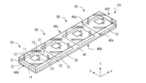
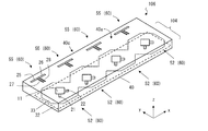
- FIG. 1 It is a perspective view showing a 1st embodiment of a plane antenna and a plane array antenna. It is a perspective view which expands and shows the planar antenna shown in FIG.
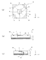
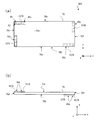
- A) is a plan view of the planar antenna shown in FIG. 1, and (b) and (c) are cross-sectional views of the planar antenna taken along lines 3B-3B and 3C-3C of (a).
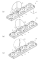
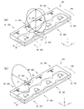
- (A)-(c) is a schematic diagram explaining the intensity distribution of the electromagnetic wave radiated from the planar antenna shown in FIG. It is a perspective view which expands and shows the plane antenna in other forms of a plane array antenna. It is a perspective view showing other forms of a plane array antenna.
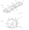
- (A) is a perspective view showing a second embodiment of a planar antenna and a planar array antenna
- (b) is a plan view of the planar antenna shown in (a). It is a perspective view which expands and shows the plane antenna in other forms of a plane array antenna. It is a perspective view showing an embodiment of a multi-axis array antenna.
- (A) And (b) is a schematic diagram explaining the intensity distribution of the electromagnetic wave radiated from the multi-axis array antenna shown in FIG. It is a typical sectional view showing an embodiment of a wireless communication module. It is a typical sectional view showing other embodiments of a wireless-communications module.
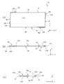
- (A) And (b) is a schematic plan view and side view which show one Embodiment of a wireless communication device.
- (A), (b) and (c) is a typical top view and side view showing other forms of a radio communications equipment.
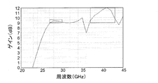
- the frequency characteristic of the peak gain of the electromagnetic wave radiated from the planar array antenna of this embodiment obtained by simulation is shown.
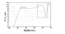
- the frequency characteristic of the peak gain of the electromagnetic wave radiated from the planar array antenna without the antenna ground conductor obtained by the simulation is shown.
- (A) is a perspective view showing other forms of a plane antenna and a plane array antenna
- (b) is a plan view of the plane antenna shown in (a).
- the frequency characteristics in the z-axis direction of electromagnetic waves radiated from the planar array antenna obtained by simulation are shown.
- the frequency characteristic of the peak gain of the electromagnetic wave radiated from the planar array antenna obtained by the simulation is shown.
- the planar antenna, planar array antenna, multi-axis antenna, wireless communication module, and wireless communication device of the present disclosure can be used for wireless communication in the quasi-microwave/centimeter wave/quasi-millimeter wave/millimeter wave band, for example.
- the wireless communication in the quasi-microwave band has a wavelength of 10 cm to 30 cm and uses a radio wave having a frequency of 1 GHz to 3 GHz as a carrier.
- the wireless communication in the centimeter wave band has a wavelength of 1 cm to 10 cm and uses a radio wave having a frequency of 3 GHz to 30 GHz as a carrier wave.
- the wireless communication in the millimeter wave band has a wavelength of 1 mm to 10 mm and uses a radio wave having a frequency of 30 GHz to 300 GHz as a carrier wave.
- the wireless communication in the quasi-millimeter wave band has a wavelength of 10 mm to 30 mm and uses a radio wave having a frequency of 10 GHz to 30 GHz as a carrier wave.
- the size of the planar antenna is on the order of a few centimeters to submillimeters.
- the planar antenna, planar array antenna or multi-axis antenna of the present disclosure is provided on the multilayer ceramic sintered substrate.
- the carrier wave frequency is 30 GHz
- the carrier wave length ⁇ is 10 mm.
- a plane antenna or a plane array antenna will be described by taking a certain case as an example.
- a right-handed Cartesian coordinate system is used to describe the arrangement, orientation, etc. of the components.
- the first right-handed orthogonal coordinate system has x, y, and z axes that are orthogonal to each other
- the second right-handed orthogonal coordinate system has u, v, and w axes that are orthogonal to each other.
- the alphabet of x, y, z, and u, v, w is added to the axes. , Which may be referred to as the first, second, and third axes.
- that two directions are aligned means that the angle formed by the two directions is in the range of 0° to about 20°.
- Parallel means that two planes, two straight lines, or the angle between the plane and the straight line is in the range of 0° to about 10°.
- FIG. 1 is a schematic perspective view showing a planar array antenna 101 of the present disclosure.
- the planar array antenna 101 includes a plurality of planar antennas 50.
- the planar antenna 50 is also called a patch antenna.
- the planar array antenna 101 includes four planar antennas 50, but the number of planar antennas 50 is not limited to four, and the planar array antenna 101 only needs to include at least two planar antennas 50.
- the plurality of planar antennas 50 are arranged in the x-axis direction.
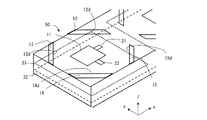
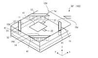
- FIG. 2 is a schematic enlarged perspective view showing one planar antenna 50 of the planar array antenna 101.
- 3A is a schematic plan view of the planar antenna 50, and FIGS. 3B and 3C are cross-sectional views taken along line 3B-3B and 3C-3C of FIG. 3A.
- Each planar antenna 50 includes a planar radiation conductor 11, a first strip conductor 21, a second strip conductor 22, parasitic conductors 12, 13, 14, and 15, an antenna ground conductor 31, and a common ground conductor 32. Equipped with.
- the planar radiating conductor 11 is arranged substantially parallel to the xy plane.
- the planar radiating conductor 11 is a radiating element that radiates radio waves, and has a shape for obtaining required radiation characteristics and impedance matching.
- the planar radiating conductor 11 has a substantially square shape having two sets of sides parallel to the x-axis direction and the y-axis direction.
- the planar radiation conductor 11 may have other shapes such as a rectangle and a circle.
- the planar radiating conductor 11 is generally configured with a size based on a length of 1 ⁇ 2 of the wavelength ⁇ of the carrier wave.
- the size of the planar radiating conductor 11 is 0.5 to 2.5 mm ⁇ 0.5 to 2.5 mm when the 28 GHz band is assumed, for example.
- the planar radiating conductor 11 has a square shape or a rectangular shape whose length in the direction parallel to at least the first strip conductor 21 resonates at f0.
- the first strip conductor 21 and the second strip conductor 22 are electromagnetically coupled to the planar radiation conductor 11 to supply signal power.
- the first strip conductor 21 extends in the x-axis direction
- the second strip conductor 22 extends in the direction orthogonal to the extending direction of the first strip conductor, that is, in the y-axis direction.
- the antenna ground conductor 31 is located between the planar radiation conductor 11 and the common ground conductor 32. Part of the first strip conductor 21 and part of the second strip conductor 22 overlap with the planar radiation conductor 11 when viewed in the z-axis direction.
- a via conductor 23 extending in the z-axis direction is connected to one end of the first strip conductor 21, for example.
- the via conductor 23 supplies signal power to the first strip conductor 21.
- the via conductor 23 penetrates holes 31c and 32c provided in the antenna ground conductor 31 and the common ground conductor 32, respectively, which will be described later, and may be connected to a wiring provided below the common ground conductor 32 or a transmission/reception circuit. Good.
- the antenna ground conductor 31 is located between the first strip conductor 21 and the second strip conductor 22, and the common ground conductor 32.
- the antenna ground conductor 31 has a rectangular shape having two sets of sides parallel to the x-axis direction and the y-axis direction, and is separated from the antenna ground conductor 31 of the adjacent planar antenna 50. ..
- the antenna ground conductor 31 overlaps at least the entire planar radiation conductor 11, and the four sides of the antenna ground conductor 31 are located outside the planar radiation conductor 11.
- the antenna ground conductor 31 is connected to the reference potential by a via conductor (not shown) or the like.
- the antenna ground conductor 31 adjusts the distribution of electromagnetic waves radiated from the planar radiation conductor 11.
- the common ground conductor 32 is a ground electrode connected to the reference potential, is larger than the planar radiation conductor 11 in the z-axis direction, and is arranged in a region including at least a region below the planar radiation conductor 11. There is. In the present embodiment, the common ground conductor 32 is connected to the common ground conductor 32 of the adjacent planar antenna 50 to form one layer.
- the planar antenna 50 includes at least a pair of parasitic conductors.
- the planar antenna 50 includes four parasitic conductors 12, 13, 14, and 15.
- Each of the parasitic conductors 12, 13, 14, and 15 forms an angle of 45 ⁇ 3° or ⁇ 45 ⁇ 3° with respect to the x-axis, and has a side facing the planar radiation conductor 11.
- the parasitic conductors 12, 13, 14, and 15 have sides 12d, 13d, 14d, and 15d, respectively.
- the sides 13d and 15d form an angle of 45 ⁇ 3° with respect to the x-axis and face the planar radiation conductor 11.
- the side 13d and the side 15d are opposed to each other with the planar radiating conductor 11 in between.
- the sides 12d and 14d form an angle of ⁇ 45 ⁇ 3° with respect to the x-axis, and face the planar radiation conductor 11.
- the side 12d and the side 14d are opposed to each other with the planar radiation conductor 11 interposed therebetween.
- the lengths of the sides 12d, 13d, 14d, and 15d are, for example, in the range of 0.5 to 2.5 mm assuming the 28 GHz band.
- the angle formed by the sides 12d, 13d, 14d, 15d and the x-axis is 45 ⁇ 3° or ⁇ 45 ⁇ 3°, an effect of suppressing unintended interference between the planar antennas 50 can be obtained as described later. To be However, it is possible to obtain this effect even if it deviates somewhat from these angles. Further, an angular deviation of about a registration error during manufacturing can be allowed.
- the angle formed by the sides 12d, 13d, 14d, 15d and the x-axis may be, for example, about 45 ⁇ 3° or ⁇ 45 ⁇ 3°. The same applies to the components arranged at 45 ⁇ 3° or ⁇ 45 ⁇ 3° with reference to the x-axis in the following embodiments.
- the parasitic conductors 12, 13, 14, 15 have strip shapes extending in the directions parallel to the sides 12d, 13d, 14d, 15d, respectively. Further, both ends of the strip shape are obliquely cut out so as to substantially coincide with the four sides of the antenna ground conductor 31 when viewed from the z-axis direction. Therefore, the parasitic conductors 12, 13, 14, and 15 have a trapezoidal shape when viewed from the z-axis direction.
- the parasitic conductors 12, 13, 14, 15 may have other shapes as long as they have the sides 12d, 13d, 14d, 15d.
- the parasitic conductors 12, 13, 14, and 15 may have a triangular shape having sides 12d, 13d, 14d, and 15d, respectively.
- the sides 12d, 13d, 14d, 15d are preferably arranged at the nodes of the electromagnetic waves emitted by the planar radiating conductor 11 or at positions near the nodes.
- the distance L from the center of the planar radiating conductor 11 to the side 12d satisfies the relationship of 0.8 ⁇ L ⁇ 1.2 ⁇ or 1.6 ⁇ L ⁇ 2.4 ⁇ , for example. It is preferable. It is preferable that the same conditions are satisfied for the positions of the sides 13d, 14d, and 15d.
- the planar radiating conductor 11 and the parasitic conductors 12, 13, 14, and 15 are located at substantially the same height in the z-axis direction.
- the planar radiation conductor 11 and the parasitic conductors 12, 13, 14, 15 are located on the same plane.
- the parasitic conductors 12, 13, 14, and 15 are elements to which power is not supplied, and are not supplied with power from the first strip conductor 21 and the second strip conductor 22.
- the planar antenna 50 has a dielectric 40, and in the present embodiment, the planar radiation conductor 11, the first strip conductor 21, the second strip conductor 22, the parasitic conductors 12, 13, 14, 15, the antenna ground conductor 31, and the antenna ground conductor 31.
- the common ground conductor 32 is arranged in the dielectric 40.
- the dielectric 40 of each planar antenna 50 is integrally formed, and has a rectangular parallelepiped shape having a long side in the x-axis direction.
- the dielectric 40 has a rectangular parallelepiped shape including a main surface 40a, a main surface 40b, and side surfaces 40c, 40d, 40e, and 40f.
- the main surface 40a and the main surface 40b are two of the six rectangular parallelepiped surfaces that are larger than the other surfaces.
- the main surface 40a and the main surface 40b are parallel to the planar radiation conductor 11, the antenna ground conductor 31, and the common ground conductor 32.
- the planar antennas 50 are arranged in the x-axis direction as described above.
- the array pitch of the plurality of planar antennas 50 in the x-axis direction is about ⁇ /2.
- each planar antenna 50 the first strip conductor 21, the second strip conductor 22, the antenna ground conductor 31, and the common ground conductor 32 are arranged in the dielectric 40.
- the planar radiation conductor 11 and the parasitic conductors 12, 13, 14, and 15 are arranged inside the main surface 40 a of the dielectric 40 or the dielectric 40. Since the planar radiation conductor 11 is an element that emits electromagnetic waves, it is preferable that the planar radiation conductor 11 is disposed on the main surface 40a from the viewpoint of improving radiation efficiency.
- planar radiating conductor 11 and the parasitic conductors 12, 13, 14, 15 are exposed on the main surface 40a, they may be deformed by an external force or the like, or may be exposed to an external environment, so that these elements may be damaged. Oxidation, corrosion, etc. may occur.
- the thickness of the dielectric covering the planar radiation conductor 11 is 70 ⁇ m or less, the planar radiation conductor 11 is formed on the main surface 40a, and further Au/Ni plating is used as a protective film. It was found that a radiation efficiency equal to or higher than that of forming a layer can be realized.
- the lower limit is not particularly limited from the viewpoint of antenna characteristics.
- the thickness t is preferably 5 ⁇ m or more. That is, the thickness t is more preferably 5 ⁇ m or more and 70 ⁇ m or less.
- the thickness t Is preferably 5 ⁇ m or more and less than 20 ⁇ m.
- the dielectric 40 may be resin, glass, ceramic or the like having a relative dielectric constant of about 1.5 to 100.
- the dielectric 40 is a multilayer dielectric in which a plurality of layers made of resin, glass, ceramics or the like are laminated.
- the dielectric 40 is, for example, a multilayer ceramic body including a plurality of ceramic layers, and the planar radiation conductor 11, the first strip conductor 21, the second strip conductor 22, and the parasitic conductors 12, 13 are provided between the plurality of ceramic layers. , 14, 15, an antenna ground conductor 31 and a common ground conductor 32 are provided, and a via conductor 23 is provided in one or more ceramic layers.
- planar radiation conductor 11 and the parasitic conductors 12, 13, 14, and 15 are provided between the same ceramic layers. However, if the distance is within the range of the above-mentioned thickness t in the z-axis direction, the planar radiation conductor 11 and the parasitic conductors 12, 13, 14, and 15 are arranged between other ceramic layers. Good.
- the distance between the respective elements can be adjusted by changing the thickness and the number of the ceramic layers arranged between the respective constituent elements.
- the constituent elements of the planar antenna 50 described above are formed of a material having electrical conductivity.
- it is formed of a material containing a metal such as Au, Ag, Cu, Ni, Al, Mo, W.
- the planar array antenna 101 can be manufactured by using a known technique using the above-mentioned dielectric material and conductive material. In particular, it can be suitably manufactured using a multilayer (laminated) substrate technology using resin, glass, or ceramic. For example, when a multilayer ceramic body is used for the dielectric 40, it can be preferably used by using a co-firing ceramic substrate technique. In other words, the planar array antenna 101 can be manufactured as a co-fired ceramic substrate.
- the co-fired ceramic substrate forming the planar array antenna 101 may be a low temperature fired ceramic (LTCC, Low Temperature Co-fired Ceramics) substrate or a high temperature fired ceramic (HTCC, High Temperature Co-fired Ceramics) substrate. May be. From the viewpoint of high frequency characteristics, it may be preferable to use a low temperature fired ceramic substrate.
- the dielectric 40, the planar radiating conductor 11, the first strip conductor 21, the second strip conductor 22, the antenna ground conductor 31, and the common ground conductor 32 are made of a ceramic material according to the firing temperature, application, frequency of wireless communication, and the like. And a conductive material is used.
- the conductive paste for forming these elements and the green sheet for forming the multilayer ceramic body of the dielectric 40 are simultaneously fired (Co-fired).
- a ceramic material and a conductive material that can be sintered in a temperature range of about 800 to 1000° C. are used.
- a ceramic material containing Al, Mg, Si, Gd, or a ceramic material containing Al, Si, Zr, or Mg is used.
- a conductive material containing Ag or Cu is used.
- the dielectric constant of the ceramic material is about 3 to 15.
- a ceramic material containing Al as a main component and a conductive material containing W (tungsten) or Mo (molybdenum) can be used.
- the LTCC material for example, an Al-Mg-Si-Gd-O-based dielectric material having a low dielectric constant (dielectric constant of 5 to 10), a crystal phase of Mg 2 SiO 4 and Si-Ba are used.
- -La-BO-based dielectric material such as glass, Al-Si-Sr-O-based dielectric material, Al-Si-Ba-O-based dielectric material, high dielectric constant (relative permittivity of 50 or more)
- Various materials such as the Bi-Ca-Nb-O-based dielectric material (1) can be used.
- Al, Si, Sr, and Ti oxides as main components
- Al, Si, Sr, and Ti as main components are Al 2 O 3 respectively.
- At least one selected from the group of Bi, Na, K, and Co as a sub-component is converted into Bi 2 O 3 in an amount of 0.1 to 10 parts by mass, and converted into Na 2 O 0.1 to 5 parts by mass, 0.1 to 5 parts by mass in terms of K 2 O, and 0.1 to 5 parts by mass in terms of CoO.
- the group of Cu, Mn and Ag It is preferable to contain at least one of 0.01 to 5 parts by mass in terms of CuO, 0.01 to 5 parts by mass in terms of Mn 3 O 4 , and 0.01 to 5 parts by mass of Ag. Other unavoidable impurities may also be contained.
- planar array antenna 101 when signal power is supplied to the planar radiating conductor 11 of each planar antenna 50 via the first strip conductor 21, as shown in FIG. 4A, the planar radiating conductor of each planar antenna 50. 11 has a maximum intensity in a direction perpendicular to the planar radiating conductor 11, that is, in the positive direction of the z-axis, and the intensity distribution F1 spread in the xz plane parallel to the extending direction of the first strip conductor 21. Emits an electromagnetic wave having.
- the planar radiating conductor 11 of each planar antenna 50 is entirely As an electromagnetic wave having a maximum intensity in a direction perpendicular to the planar radiating conductor 11, that is, in the positive direction of the z-axis, and having an intensity distribution F2 spread in the yz plane parallel to the extending direction of the second strip conductor 22. discharge.
- the electromagnetic wave having the intensity distribution F1 and the electromagnetic wave having the intensity distribution F2 are combined to generate an electromagnetic wave having the intensity distribution F12. Is released.
- the electromagnetic wave having the intensity distribution F12 is a surface obtained by rotating the xz plane around the z axis by 45 ⁇ 3° with respect to the x axis and a surface obtained by rotating the xz plane around the z axis by ⁇ 45 ⁇ 3° about the x axis. Has spread to.
- the parasitic conductors 12, 13, 14, and 15 having sides that form an angle of 45 ⁇ 3° or ⁇ 45 ⁇ 3° with respect to the x-axis reflect or attenuate the combined electromagnetic waves, and the adjacent planes. It is possible to suppress adverse effects such as unintended interference on electromagnetic waves emitted from the antenna 50.
- the electromagnetic wave of intensity distribution F1 due to the signal power supplied from the first strip conductor 21 and the electromagnetic wave of intensity distribution F2 due to the signal power supplied from the second strip conductor 22 are orthogonal to each other. Therefore, even if signal power is simultaneously supplied from the first strip conductor 21 and the second strip conductor 22 to the planar radiation conductor 11, the combined electromagnetic wave is received and the generated signal is separated into two signals. Is possible. Therefore, according to the planar array antenna 101, different signal powers can be radiated from the planar radiating conductor 11 via the first strip conductor 21 and the second strip conductor 22, and more information can be transmitted and received. Is possible. Further, in the planar array antenna 101, since adverse effects due to interference between the planar antennas 50 can be suppressed, a planar array antenna capable of performing beamforming with higher directivity can be realized.
- the parasitic conductors 12, 13, 14, and 15 can suppress undesired spread of electromagnetic waves as described above. Therefore, even when the planar antenna 50 is arranged alone in the wireless device, it is possible to suppress undesired effects on the circuits arranged around the planar antenna 50 and other antennas.
- the planar array antenna 101 can exert an excellent effect when different signal powers are simultaneously input to the first strip conductor 21 and the second strip conductor 22 and two electromagnetic waves are combined and radiated.
- Signal power may be input to one of the first strip conductor 21 and the second strip conductor 22 to radiate electromagnetic waves.
- the parasitic conductors 12, 13, 14, and 15 can suppress adverse effects between the planar antennas 50, a planar array antenna capable of performing beamforming with higher directivity can be realized.
- orthogonal polarizations such as vertically polarized waves and horizontally polarized waves can be transmitted and received with high quality and at the same time by the planar radiation conductor 11, so that the communication speed can be improved.
- the planar array antenna 101 can improve the coverage mainly on the zx plane of FIG. 1 by providing a phase difference and an amplitude difference to the incident signal power between the planar antennas 50 and performing beam forming. Become.
- FIG. 5 is an enlarged perspective view showing one of the planar antennas 50 ′ of the planar array antenna 102.
- the planar array antenna 102 includes a plurality of planar antennas 50′, and the planar antenna 50′ further includes at least one first via conductor 41 connecting the parasitic conductors 12, 13, 14, 15 and the antenna ground conductor 31. It differs from the planar array antenna 101 in that it is provided.
- the planar antenna 50' includes a plurality of first via conductors 41 arranged between the parasitic conductors 12, 13, 14, 15 and the antenna ground conductor 31, respectively.
- a plurality of first via conductors 41 arranged in a direction forming an angle of ⁇ 45 ⁇ 3° with respect to the x-axis are arranged between the parasitic conductor 12 and the antenna ground conductor 31. .. One end of each first via conductor is connected to the parasitic conductor 12, and the other end is connected to the antenna ground conductor 31.
- the plurality of first via conductors 41 are also provided between the parasitic conductor 13 and the antenna ground conductor 31, between the parasitic conductor 14 and the antenna ground conductor 31, and between the parasitic conductor 15 and the antenna ground conductor 31. Are arranged.
- the diameter of the first via conductor 41 is, for example, several ⁇ m to several hundreds of ⁇ m, and the pitch (axial distance) of the first via conductor 41 is, for example, 1/8 ⁇ d, preferably 1/16 ⁇ d or less.
- the gaps are provided between the plurality of first via conductors 41 in FIG. 5, the side surfaces of the first via conductors 41 may be in contact with each other.
- the plurality of first via conductors 41 arranged between the parasitic conductors 12, 13, 14, 15 and the antenna ground conductor 31 function as shields. Therefore, the electromagnetic waves radiated from the planar radiating conductor 11 of each planar antenna 50' are confined in the area surrounded by the plurality of first via conductors 41 and are less likely to leak to the adjacent planar antenna 50'. Therefore, it is possible to realize a planar array antenna capable of suppressing the adverse effect between the planar antennas 50' and performing beamforming with higher directivity.
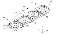
- FIG. 6 is a perspective view of the planar array antenna 103.
- the planar array antenna 103 is a planar array antenna in that it includes a plurality of second via conductors 42 arranged in the y-axis direction between at least one pair of adjacent planar antennas 50 among the plurality of planar antennas 50. Different from 101.
- the second via conductor 42 extends along the z-axis direction and has one end connected to the common ground conductor 32.
- the second via conductor 42 preferably has a height in the z-axis direction that is approximately the same as or greater than the distance between the common ground conductor 32 and the planar radiation conductor 11.
- the planar array antenna 103 includes a plurality of second via conductors 42 arranged in the y-axis direction between each pair of planar antennas 50.
- One or two rows of the second via conductors 42 arranged in the y-axis direction are arranged between the planar antennas 50.
- two rows of the second via conductors 42 are arranged between the second and third planar antennas 50 in the x-axis direction among the four planar antennas 50.
- the second via conductors 42 When one row of the second via conductors 42 is arranged between the planar antennas 50, the second via conductors 42 are not connected to the antenna ground conductors 31 of the two planar antennas 50 sandwiching the second via conductors, and are separated from each other. doing. When two rows of the second via conductors 42 are arranged between the planar antennas 50, the second via conductors 42 may be respectively connected to the antenna ground conductors 31 of the two planar antennas 50 sandwiching the second via conductors. ..
- the diameter of the second via conductor 42 is, for example, several ⁇ m to several 100 ⁇ m, and the pitch (axial distance) of the second via conductor 42 is, for example, 1/8 ⁇ d, preferably 1/16 ⁇ d. It is as follows. Although the gaps are provided between the plurality of second via conductors 42 in FIG. 6, the side surfaces of the second via conductors 42 may be in contact with each other.
- the plurality of second via conductors 42 arranged in the y-axis direction between the pair of planar antennas 50 function as shields, and electromagnetic waves emitted from the planar radiation conductor 11 of the planar antenna 50 leak to the adjacent planar antenna 50. Suppress the collapse. Therefore, it is possible to realize a planar array antenna capable of suppressing adverse effects between the planar antennas 50 and performing beamforming with higher directivity.
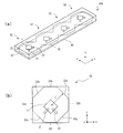
- FIG. 7A is a schematic perspective view showing the planar array antenna 104 of the present disclosure.
- FIG. 7B is a schematic enlarged perspective view showing one flat antenna 52 of the flat array antenna 104.
- the planar array antenna 104 includes a plurality of planar antennas 52 arranged in the x-axis direction.
- Each planar antenna 52 includes a planar radiating conductor 11, a first strip conductor 21, a second strip conductor 22, an antenna ground conductor 33, and a common ground conductor 32.
- the arrangement of the planar radiation conductor 11, the first strip conductor, the second strip conductor 22, the antenna ground conductor 33, and the common ground conductor 32 in the z-axis direction is the same as that of the planar antenna 50 of the planar array antenna 101.
- the planar radiating conductor 11, the first strip conductor 21, and the second strip conductor 22 are arranged in a direction rotated by ⁇ 45 ⁇ 3° around the z axis as compared with the planar antenna 50.
- the second strip conductor 22 extends in a direction orthogonal to the extending direction of the first strip conductor 21.
- the planar radiating conductor 11 has a substantially square shape having two sets of sides parallel to a straight line forming an angle of 45 ⁇ 3° and a straight line forming an angle of ⁇ 45 ⁇ 3° with respect to the x-axis.
- the antenna ground conductor 33 has at least a pair of sides on its outer edge that make an angle of 45 ⁇ 3° or ⁇ 45 ⁇ 3° with respect to the x-axis.
- the antenna ground conductor 33 has sides 33a to 33h at the outer edge.
- the sides 33a and 33e form an angle of ⁇ 45 ⁇ 3° with respect to the x-axis
- the sides 33c and 33g form an angle of 45 ⁇ 3° with respect to the x-axis.
- It also has sides 33b and 33f parallel to the x-axis, and sides 33d and 33h parallel to the y-axis.
- the sides 33a and 33e and the sides 33c and 33g are positioned so as to sandwich the planar radiation conductor 11, respectively.
- the antenna ground conductor 33 is connected to the antenna ground conductor 33 of the adjacent planar antenna 52. Specifically, except for the planar antennas 52 at both ends in the x-axis direction, the side 33d of the antenna ground conductor 33 is connected to the side 33h of the antenna ground conductor 33 of the adjacent planar antenna 52. In the planar antennas 52 located at both ends in the x-axis direction, the sides 33h or 33d of the antenna ground conductor 33 are connected to the sides 33d or 33h of the antenna ground conductor 33 of the adjacent planar antenna 52, respectively.
- the sides 33a, 33c, 33e, 33g are preferably arranged at the nodes of the electromagnetic waves emitted by the planar radiating conductor 11 or at positions near the nodes.
- the distance L′ from the center of the planar radiating conductor 11 to the side 33a is, for example, 0.8 ⁇ L′ ⁇ 1.2 ⁇ or 1.6 ⁇ L′ ⁇ 2.4 ⁇ . It is preferable that the relationship of is satisfied. It is preferable that the positions of the sides 33c, 33e, and 33g also satisfy the same condition.
- each planar antenna 52 of the planar array antenna 104 when signal power is supplied to the planar radiating conductor 11 via the first strip conductor 21 and the second strip conductor 22, the combined wave of electromagnetic waves by the two signal powers is z-axis. Emit an electromagnetic wave having a maximum intensity in the positive direction of, and an intensity distribution spread in the xz plane and the yz plane.
- the planar antennas 52 are arranged in the x-axis direction at an equal pitch or a pitch close thereto. Further, the planar radiation conductor 11, the first strip conductor 21, and the second strip conductor 22 are arranged so as to be rotated in a direction forming an angle of ⁇ 45 ⁇ 3 degrees with the longitudinal direction.
- the sides 33a, 33e and 33c, 33g of the antenna ground conductor 33 are located in the two resonance directions (directions of 45° and ⁇ 45° with respect to the x axis) of the planar antenna 52, and the planar antenna 52
- the electromagnetic length (resonator length) is equal in the two resonance directions, and the influence of unintended interference from the adjacent antenna can be reduced.
- planar array antenna 104 since the antenna ground conductor 33 of each planar antenna 52 has the sides 33a, 33c, 33e, 33g forming the above-mentioned angle with respect to the x-axis, these sides are The electromagnetic waves are reflected or attenuated, and adverse effects such as unintended interference with the electromagnetic waves emitted from the adjacent planar antenna 52 are suppressed. Therefore, a planar array antenna capable of performing beamforming with higher directivity can be realized.
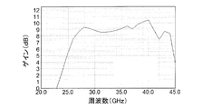
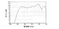
- FIG. 15 shows the frequency characteristics of the peak gain of the electromagnetic wave radiated from the planar array antenna 104 of this embodiment obtained by simulation.
- the horizontal axis represents frequency and the vertical axis represents the maximum gain that can be achieved regardless of azimuth.
- FIG. 16 shows the frequency characteristic of the peak gain of the planar antenna having no antenna ground conductor 33.
- a gain of 9 dB or more is obtained in two frequency bands of 27 GHz to 30 GHz and 37 GHz to 43 GHz. Particularly, in the band of 37 GHz to 43 GHz, a maximum gain of 12 dB is obtained.
- FIG. 15 shows the frequency characteristics of the peak gain of the electromagnetic wave radiated from the planar array antenna 104 of this embodiment obtained by simulation.
- the horizontal axis represents frequency and the vertical axis represents the maximum gain that can be achieved regardless of azimuth.
- FIG. 16 shows the frequency characteristic of the peak gain of the planar antenna having no antenna ground conductor 33.
- a gain of 9 dB or more is obtained in two
- the gain is greatly reduced at a frequency of 41 GHz or higher in the band of 37 GHz to 43 GHz. It is considered that this is because at a frequency of 41 GHz or higher, the electromagnetic waves emitted from the adjacent planar antennas 52 interfere with each other to reduce the gain.
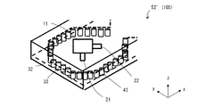
- FIG. 8 is an enlarged perspective view showing one of the planar antennas 52 ′ of the planar array antenna 105.
- the planar array antenna 105 includes a plurality of planar antennas 52′, and the planar antenna 52′ further includes at least one third via conductor 43 that connects the antenna ground conductor 33 and the common ground conductor 32.
- the planar antenna 52' includes a plurality of third via conductors 43.
- the plurality of third via conductors 43 are arranged along the outer edge of the antenna ground conductor 33, one end thereof is connected to the antenna ground conductor 33, and the other end thereof is connected to the common ground conductor 32.
- the diameter and pitch of the third via conductor 43 may be similar to those of the second via conductor 42. Further, in FIG. 8, a gap is provided between the plurality of third via conductors 43, but the side surfaces of the third via conductors 43 may be in contact with each other.
- the plurality of third via conductors 43 function as a shield and suppress electromagnetic waves emitted from the planar radiating conductor 11 of the planar antenna 50 from leaking into the adjacent planar antenna 50. Therefore, it is possible to realize a planar array antenna capable of suppressing the adverse effect between the planar antennas 52' and performing beamforming with higher directivity.
- FIG. 17A is a perspective view of the planar antenna 52' and the planar array antenna 111
- FIG. 17B is a plan view of the planar antenna shown in FIG.
- the planar antenna 52′ and the planar array antenna 111 are the second embodiment in that the width Lc of the common ground conductor 32 in the direction parallel to the y-axis is smaller than the maximum width La of the antenna ground conductor 33 parallel to the y-axis. It differs from the planar antenna 52 and the planar array antenna 104 of the configuration.
- the maximum width La of the antenna ground conductor 33 parallel to the y-axis means, for example, the distance between the side 33b and the side 33f, as shown in FIG. 17(b).
- the width Lc of the common ground conductor 32 in the direction parallel to the y-axis and the maximum width La of the antenna ground conductor 33 parallel to the y-axis satisfy the relationship of the following expression (1) as described above. It is preferable that La and Lc satisfy the relationship of the following expression (2), and it is more preferable that the relationship of the expression (3) is satisfied.
- ⁇ is the wavelength of the carrier wave and ⁇ is the relative permittivity of the dielectric 40.
- Lc ⁇ La (1) Lc ⁇ La ⁇ ( ⁇ /16)/( ⁇ ) (2) Lc ⁇ La-( ⁇ /12)/( ⁇ ) (3) More preferably, the formula (4) is satisfied.
- each planar antenna 52′ has an interaction between the planar antennas 52′ and the planar array antenna 111 having a rectangular shape in plan view, in particular, the common ground conductor 32 is longer in the X-axis direction than in the Y-axis direction. If there is no such feature, it has the maximum intensity in the direction perpendicular to the planar radiation conductor 11, that is, in the positive direction of the z-axis. However, depending on the condition of interaction between the planar antennas 52 ′ and the asymmetry of the shape of the common ground conductor 21, the direction of maximum intensity of the radiated electromagnetic wave may be inclined.
- the width Lc of the common ground conductor 32 in the direction parallel to the y-axis is made smaller than the maximum width La of the antenna ground conductor 33 parallel to the y-axis to effectively contribute to the radiation of electromagnetic waves.
- the condition of proper grounding is mainly determined by the antenna ground conductor 33, and the influence of the shape of the common ground conductor 32 is reduced. Therefore, it becomes possible to make the direction of the maximum intensity of the radiated electromagnetic wave closer to the positive direction of the z axis.
- FIG. 18 shows frequency characteristics in the z-axis direction of electromagnetic waves radiated from the planar array antenna 111 obtained by simulation.
- the horizontal axis represents frequency
- the vertical axis represents gain in the positive direction of the z axis.
- FIG. 19 shows the frequency characteristics of the peak gain of the electromagnetic waves emitted from the planar array antenna 111.
- the horizontal axis represents frequency
- the vertical axis represents the maximum gain that can be achieved regardless of azimuth.
- the frequency characteristic in the z-axis direction is in good agreement with the frequency characteristic of the peak gain of the electromagnetic wave radiated from the planar array antenna 111, and is radiated in the range of 20 GHz to 45 GHz. It can be seen that the intensity of the electromagnetic wave in the z-axis direction is maximum.
- FIG. 9 is a schematic perspective view showing the multi-axis array antenna 106 of the present disclosure.
- the multi-axis array antenna 106 includes the planar array antenna 104 and a plurality of linear antennas 55.
- the planar array antenna 104 has the same structure as the planar array antenna 104 described in the second embodiment.
- the multi-axis array antenna 106 may include any of the planar array antennas 101 to 103 and 105 of the first and second embodiments, in addition to the planar array antenna 104.
- Each of the plurality of linear antennas 55 corresponds to one of the plurality of planar antennas 52 of the planar array antenna 104, and is arranged apart in the y-axis direction.
- Each linear antenna 55 includes one or two linear radiating conductors extending parallel to the x-axis direction.
- the linear antenna 55 includes the linear radiating conductors 25 and 26.
- the linear radiating conductors 25 and 26 each have a stripe shape extending in the x-axis direction and are arranged close to each other in the x-axis direction.
- One planar antenna 52 and one linear antenna 55 arranged in the y-axis direction constitute one antenna unit 60.
- the linear antenna 55 further includes feed conductors 27 and 28 for supplying signal power to the linear radiating conductors 25 and 26.
- the power supply conductors 27 and 28 have a stripe shape extending in the y-axis direction. One ends of the power supply conductors 27 and 28 are connected to one ends of the linear radiation conductors 25 and 26 that are arranged adjacent to each other.
- the linear radiating conductors 25 and 26 of the linear antenna 55 may or may not overlap the common ground conductor 32 when viewed from the z-axis direction.
- the linear radiation conductors 25 and 26 of the linear antenna 55 do not overlap with the common ground conductor 32 when viewed from the z-axis direction, the linear radiation conductors 25 and 26 of the linear antenna 55 in the y-axis direction It is preferable to be separated from the edge of the common ground conductor 32 by ⁇ /8 or more.
- the common ground conductor 32 and the linear radiation conductors 25 and 26 are ⁇ /8 in the z-axis direction. It is preferable that they are separated from each other.
- a part of the linear antenna 55 including the other ends of the feeding conductors 27 and 28 may overlap the common ground conductor 32 when viewed from the z-axis direction.
- One of the other ends of the power supply conductors 27 and 28 is connected to the reference potential, and the other is supplied with signal power.
- the length of the linear radiation conductors 25 and 26 in the x-axis direction is, for example, about 1.2 mm.
- the length (width) in the y-axis direction is, for example, about 0.2 mm.
- the multi-axis array antenna 106 when signal power is simultaneously supplied to the plane antenna 52 of each antenna unit 60 via the first strip conductor 21 and the second strip conductor 22, as shown in FIG.
- the planar radiation conductor 11 as a whole emits an electromagnetic wave having an intensity distribution F +z having a maximum intensity in a direction perpendicular to the planar radiation conductor 11, that is, in the positive direction of the z axis.
- the planar radiating conductor 11 of each antenna unit 52 has a positive z-axis.
- the planar antenna 52 and the linear antenna 55 may be used at the same time or may be selectively used.
- an RF switch or the like is used.
- the signal to be transmitted/received may be selectively input to the plane antenna 52 or the linear antenna 55.
- a phase difference to the signals input to the planar antenna 52 and the linear antenna 55.
- a signal to be transmitted/received may be selectively input to the planar antenna 52 or the linear antenna 55 using a phase shifter including a diode switch or a MEMS switch.
- the multi-axis antenna 106 includes a plurality of antenna units 60. Therefore, it is possible to perform beamforming of electromagnetic waves emitted from the planar antenna 52 and the linear antenna 55.
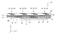
- FIG. 11 is a schematic cross-sectional view of the wireless communication module 107 on the xz plane.
- the wireless communication module 107 includes, for example, the multi-axis array antenna 106 of the third embodiment, active elements 64 and 65, passive elements 66, and a connector 67.
- the wireless communication module 107 is also called an antenna in package.
- the wireless communication module 107 may include a cover 68 that covers the active elements 64, 65 and the passive element 66.
- the cover 68 is made of metal or the like and has the functions of an electromagnetic shield, a heat sink, or both.
- the active element 64, 65 and the passive element 66 may be molded with the sealing resin 71 instead of the cover 68.
- the active elements 64 and 65 and the passive element 66 may be molded with the sealing resin 71, and the outside of the sealing resin 71 may be covered with the cover 68.
- the connector 67 may be a surface mount type high frequency coaxial connector or a low frequency multi-pole connector.
- a conductor 61 and a via conductor 62 that form a wired circuit pattern for connecting to the planar antenna 52 and the linear antenna 55 are provided on the main surface 40b side of the common ground conductor 32 of the dielectric 40 of the multi-axis array antenna 106. It is provided. An electrode 63 is provided on the main surface 40b. In the xz section shown in FIG. 11, the components of the linear antenna 55 are not shown.
- the active elements 64 and 65 are DC/DC converters, low noise amplifiers (LNA), power amplifiers (PA), high-frequency ICs, etc., and the passive elements 66 are capacitors, coils, RF switches, etc.
- the connector 67 is a connector for connecting the wireless communication module 107 and the outside.
- the active elements 64, 65, the passive element 66, and the connector 67 are connected to the electrode 63 of the main surface 40b of the dielectric 40 of the multi-axis array antenna 106 by soldering or the like, so that the main surface 40b of the multi-axis array antenna 106 is connected. It is implemented.
- the wiring circuit formed by the conductor 61 and the via conductor 62, the active elements 64 and 65, the passive element 66, and the connector 67 form a signal processing circuit and the like.
- the main surface 40a where the planar antenna 52 and the linear antenna 55 are close to each other is located on the opposite side to the main surface 40b to which the active elements 64, 65 and the like are connected. Therefore, the electromagnetic waves are radiated from the planar antenna 52 and the linear antenna 55 without being affected by the active elements 64 and 65, and the electromagnetic waves such as the quasi-millimeter wave and the millimeter wave band that arrive from the outside are received by the planar antenna 52. And the linear antenna 55 can receive. Therefore, a compact wireless communication module can be realized by including an antenna capable of selectively transmitting and receiving electromagnetic waves in two orthogonal directions.
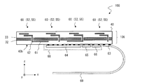
- the electrodes 63 of the multi-axis array antenna 106 are electrically connected to the flexible wiring 69.
- the flexible wiring 69 is, for example, a flexible printed board on which a wiring circuit is formed, a coaxial cable, a liquid crystal polymer substrate, or the like.
- liquid crystal polymers are excellent in high frequency characteristics, and thus can be suitably used as a wiring circuit for the multi-axis array antenna 106.
- 13A and 13B are a schematic plan view and a side view of the wireless communication device 109.
- the wireless communication device 109 includes a main board (circuit board) 70 and one or more wireless communication modules 107.
- the wireless communication device 109 includes four wireless communication modules 107A to 107D.
- the main board 70 includes electronic circuits necessary to realize the functions of the wireless communication device 109, a wireless communication circuit, and the like.
- a geomagnetic sensor In order to detect the posture and position of the main board 70, a geomagnetic sensor, a GPS unit, etc. may be provided.
- the main board 70 has main surfaces 70a, 70b and four side portions 70c, 70d, 70e, 70f.
- the main surfaces 70a and 70b are perpendicular to the w axis in the second right-handed orthogonal coordinate system
- the side portions 70c and 70e are perpendicular to the v axis
- the side portions 70d and 70f are perpendicular to the u axis.
- the main board 70 is schematically shown as a rectangular parallelepiped having a rectangular main surface, but each of the side portions 70c, 70d, 70e, and 70f may be composed of a plurality of surfaces.
- the wireless communication device 109 includes one or more wireless communication modules.
- the number of wireless communication modules can be adjusted according to the specifications of the wireless communication device such as in which direction the electromagnetic waves are transmitted and received, the sensitivity of the transmission and reception, and the required performance.
- the arrangement of the wireless communication module on the main board 70 is also based on electromagnetic interference with other wireless communication modules and other functional modules in the wireless communication device, interference with the arrangement, and transmission/reception of electromagnetic waves when the wireless communication device is packaged through the exterior. It can be determined at any position in consideration of sensitivity.
- the wireless communication module When arranging the wireless communication module on the main surfaces 70a and 70b of the main board 70, if the position is close to one of the side portions 70c, 70d, 70e, and 70f, the other circuits and the like provided on the main board 70 May be less susceptible to interference.
- the arrangement of the wireless communication modules on the main surfaces 70a, 70b is not limited to the position close to the side portions 70c, 70d, 70e, 70f, and may be the center of the main surfaces 70a, 70b.
- the side surface 40c of the dielectric 40 of the multi-axis array antenna 106 is close to one of the side portions 70c, 70d, 70e, 70f, and the dielectrics
- the main surface 40a of 40 is arranged on the main surface 70a or the main surface 70b so as to be located on the side opposite to the main board 70.
- the linear radiation conductors 25 and 26 of the linear antenna 55 are close to the side surface 40c of the dielectric 40, and electromagnetic waves are radiated from the side surface 40c.
- the main surface 40a of the dielectric 40 is close to the planar radiation conductor 11 of the planar antenna 52, and electromagnetic waves are radiated from the main surface 40a.
- the radio communication modules 107A to 107D are arranged on the main board 70 at positions and directions where electromagnetic waves emitted from the radio communication modules 107A to 107D are less likely to interfere with the main board 70.
- the wireless communication modules 107A to 107D may be close to each other or separated from each other in the uvw direction.
- the wireless communication modules 107A and 107C are arranged on the main surface 70a so that the side surfaces 40c of the wireless communication modules 107A and 107C are close to either of the side portions 70c and 70d.
- the wireless communication modules 107B and 107D are arranged on the main surface 70b so that the side surface 40c of the wireless communication modules 107B and 107D is close to either of the side portions 70e and 70f.
- the side surface 40c of the wireless communication module 107A is close to the side portion 70c
- the side surface 40c of the wireless communication module 107B is close to the side portion 70e.
- the side surface 40c of the wireless communication module 107C is close to the side portion 70d, and the side surface 40c of the wireless communication module 107D is close to the side portion 70f.
- the wireless communication modules 107A to 107D are arranged in point symmetry with respect to the center of the main board 70.
- electromagnetic waves can be emitted to the main board 70 in all directions ( ⁇ u, ⁇ v, ⁇ w directions).
- the GPS unit of the wireless communication device 109 detects the position, the closest base station among the plurality of base stations around the wireless communication device 109 whose position information is known, and the wireless communication device of the base station.
- the azimuth from 109 can be determined.
- the geomagnetic sensor of the wireless communication device 109 the attitude of the wireless communication device 109 can be determined, and in the current attitude of the wireless communication device 109, the determined base station to radiate an electromagnetic wave with the strongest intensity. It is possible to determine the wireless communication modules 107A to 107D and the planar antenna 52/the linear antenna 55 that can be used. Therefore, high-quality communication can be performed by transmitting and receiving electromagnetic waves using the determined wireless communication module and antenna.
- the wireless communication modules 107A to 107D may be arranged on the side of the main board 70.
- 14A, 14B, and 14C are a schematic plan view and a side view of the wireless communication device 110.
- the side surface 40c of the dielectric 40 of the multi-axis array antenna 106 is close to the main surface 70a or the main surface 70b, and the main surface 40a of the dielectric 40 is the main board 70. It is arranged on any of the side portions 70c to 70f so as to be located on the opposite side.
- the wireless communication modules 107A and 107B are arranged on the side portions 70c and 70e so that the side surfaces 40c of the wireless communication modules 107A and 107B are close to either of the main surfaces 70a and 70b. Further, the wireless communication modules 107C and 107D are arranged on the side portions 70d and 70f so that the side surfaces 40c of the wireless communication modules 107C and 107D are close to either of the main surfaces 70a and 70b. In this embodiment, the side surface 40c of the wireless communication module 107A is close to the main surface 70a, and the side surface 40c of the wireless communication module 107B is close to the main surface 70b.
- the side surface 40c of the wireless communication module 107C is close to the main surface 70a, and the side surface 40c of the wireless communication module 107D is close to the main surface 70b.
- the wireless communication modules 107A to 107D are arranged in point symmetry with respect to the center of the main board 70.
- the positions of the wireless communication modules 107A to 107D in the w-axis direction may be displaced from the center of the main board 70 in the w-axis direction.
- the wireless communication modules 107A to 107D may be in contact with the side portions 70c to 70f of the main board 70, or may be arranged with a gap.
- the wireless communication device 110 can cause the main board 70 to emit electromagnetic waves in all directions ( ⁇ u, ⁇ v, ⁇ w directions).
- the arrangement of the wireless communication module 107 in the wireless communication device is not limited to the above embodiment, and various modifications can be made.
- some of the plurality of wireless modules are arranged on at least one of the main surfaces 70a, 70b of the main board 70, and the remaining wireless modules are arranged on at least one of the side portions 70c, 70d, 70e, 70f. You may.
- planar array antenna and the like described in the first to fifth embodiments can be implemented in an appropriate combination.
- the feature that the width of the common ground conductor in the y-axis direction is smaller than the maximum width of the antenna ground conductor in the y-axis direction can be combined with any other embodiment of the first to fifth embodiments. is there.
- the number of planar antennas in the planar array antenna is not limited to the value shown in the embodiment.
- the planar array antenna may be arranged two-dimensionally in the x-axis direction and the y-axis direction.
- the shape of the planar radiation conductor is not limited to the illustrated shape.
- planar antenna, planar array antenna, multi-axis array antenna, wireless communication module, and wireless communication device of the present disclosure can be suitably used for various high-frequency wireless communication antennas and wireless communication circuits including the antennas. It is preferably used for wireless communication devices in the quasi-microwave/centimeter wave/quasi-millimeter wave/millimeter wave band.
Landscapes
- Variable-Direction Aerials And Aerial Arrays (AREA)
- Waveguide Aerials (AREA)
- Details Of Aerials (AREA)
- Support Of Aerials (AREA)
Abstract
平面アンテナは、平面状放射導体11と、共通地導体32と、平面状放射導体11と、共通地導体32との間に位置し、第1、第2および第3軸を有する第1右手直交座標系において、第1軸に平行な方向に伸びる第1ストリップ導体21と、平面状放射導体と、共通地導体との間に位置し、第1ストリップ導体の伸びる方向と直交する方向に伸びる第2ストリップ導体22と、第1軸に対して45±3°または-45±3°の角度をなしており、平面状放射導体と対向している辺を有する少なくとも一対の無給電導体12~15とを備えている。
Description
本願は、平面アンテナ、平面アレイアンテナ、多軸アレイアンテナ、無線通信モジュールおよび無線通信装置に関する。
インターネット通信の増大、高画質の映像技術の開発に伴い、無線通信に求められる通信速度も増大しており、より多くの情報が送受信可能な高周波の無線通信技術が求められている。搬送波の周波数が高くなると、電磁波の直進性が高まるため、無線端末との間で電波の送受信を行う基地局の通信可能なセル半径は小さくなる。このため、短波長の搬送波を用いる無線通信では、一般に、従来よりも高い密度で基地局が配置される。
その結果、無線通信端末から、近い距離にある基地局の数は増えることになり、近接する複数の基地局のなかから、高品質で通信が可能な特定の基地局を選択することが必要となる場合がある。つまり、放射可能な方位が広く、かつ、指向性が高いアンテナが求められる場合がある。
例えば、特許文献1は、電波の強度の強い方向から受信を行うためのダイバーシティーアンテナを開示している。
本願は、短波長の帯域において、高い指向性を有する電磁波の送受信が可能な平面アンテナ、平面アレイアンテナ、多軸アレイアンテナ、無線通信モジュールおよび無線通信装置を提供する。
本開示の一実施形態による平面アンテナは、平面状放射導体と、共通地導体と、前記平面状放射導体と、前記共通地導体との間に位置し、第1、第2および第3軸を有する第1右手直交座標系において、第1軸に平行な方向に伸びる第1ストリップ導体と、前記平面状放射導体と、前記共通地導体との間に位置し、前記第1ストリップ導体の伸びる方向と直交する方向に伸びる第2ストリップ導体と、前記第1軸に対して45±3°または-45±3°の角度をなしており、前記平面状放射導体と対向している辺を有する少なくとも一対の無給電導体とを備える。
平面アンテナは、前記第1軸に対して45±3°の角度をなしており、前記平面状放射導体と対向している辺を有する前記一対の無給電導体と、前記第1軸に対して-45±3°の角度をなしており、前記平面状放射導体と対向している辺を有する他の一対の無給電導体と、を備えていてもよい。
前記平面状放射導体と、前記無給電導体とは同一平面上に位置していてもよい。
平面アンテナは、前記第1ストリップ導体および前記第2ストリップ導体と、前記共通地導体との間に位置するアンテナ地導体をさらに含み、前記アンテナ地導体は、前記第3軸方向からみて、少なくとも前記平面状放射導体全体と重なっていてもよい。
平面アンテナは、前記無給電導体と前記アンテナ地導体とを接続する少なくとも1つの第1ビア導体をさらに備えていてもよい。
平面アンテナは、前記第3軸方向に垂直な主面を有する誘電体をさらに備え、前記平面状放射導体、前記共通地導体、前記第1ストリップ導体、前記第2ストリップ導体および前記無給電導体は前記誘電体内に位置していてもよい。
本開示の一実施形態による平面アレイアンテナは、前記第1軸方向に配列された、複数の上記平面アンテナを備え、各平面アンテナの誘電体は一体的に構成されており、各平面アンテナの共通地導体は互いに接続されており、各平面アンテナのアンテナ地導体は、互いに分離している。
平面アレイアンテナは、前記複数の平面アンテナのうち、少なくとも1つの隣接する一対の平面アンテナにおいて、前記第3軸に沿って伸び、前記第2軸と平行に配列された複数の第2ビア導体を備え、前記複数の第2ビア導体は、前記共通地導体と接続されていてもよい。
前記複数の第2ビア導体は、前記隣接する一対の平面アンテナの一方のアンテナ地導体とさらに接続された第1列と、前記隣接する一対の平面アンテナの他方のアンテナ地導体とさらに接続された第2列とを含んでいてもよい。
前記複数の第2ビア導体は、前記第3軸と平行な方向において、前記共通地導体と前記平面状放射導体との距離と以上の高さを有していてもよい。
本開示の他の実施形態による平面アンテナは、平面状放射導体と、共通地導体と、前記平面状放射導体と、前記共通地導体との間に位置し、第1、第2および第3軸を有する第1右手直交座標系において、第1軸に対して45±3°の角度をなす方向に伸びる第1ストリップ導体と、前記平面状放射導体と、前記共通地導体との間に位置し、前記第1ストリップ導体の伸びる方向と直交する方向に伸びる第2ストリップ導体と、前記第1ストリップ導体および前記第2ストリップ導体と、前記共通地導体との間に位置し、前記第1軸に対して45±3°または-45±3°の角度をなす少なくとも一対の辺を外縁に有するアンテナ地導体と、を備える。
前記アンテナ地導体は、前記第3軸方向から見て、前記第1軸に対して45±3°の角度をなしており、前記平面状放射導体を挟む前記一対の辺と、前記第1軸に対して-45±3°の角度をなしており、前記平面状放射導体を挟む他の一対の辺と、を備えていてもよい。
平面アンテナは、前記アンテナ地導体の前記外縁に沿って位置し、前記アンテナ地導体と前記共通地導体とを接続する少なくとも1つの第3ビア導体をさらに備えていてもよい。
平面アンテナは、前記第3軸方向に垂直な主面を有する誘電体をさらに備え、前記平面状放射導体、前記共通地導体、前記第1ストリップ導体、前記第2ストリップ導体および前記無給電導体は前記誘電体内に位置していてもよい。
本開示のある実施形態による平面アレイアンテナは、前記第1軸方向に配列された、複数の上記平面アンテナを備え、各平面アンテナの誘電体は一体的に構成されており、各平面アンテナの共通地導体は互いに接続されており、各平面アンテナのアンテナ地導体は互いに接続されている。
平面アレイアンテナは、前記複数の平面アンテナのうち、少なくとも1つの隣接する一対の平面アンテナにおいて、前記第3軸に沿って伸び、前記第2軸と平行に配列された複数の第2ビア導体を備え、前記複数の第2ビア導体は、前記共通地導体と接続されていてもよい。
本開示のある実施形態による多軸アレイアンテナは、上記いずれかに記載の平面アレイアンテナと、複数の線状アンテナと、を備え、各線状アンテナは、前記複数の平面アンテナの1つに対して、前記第2軸方向に離間して位置し、前記第1軸と平行に伸びる1つまたは2つの線状放射導体を含む。
前記誘電体は、前記主面に隣接し、かつ、前記第2軸に垂直な側面を有し、前記線状アンテナの前記1つまたは2つの線状放射導体は、前記側面に近接して前記誘電体内に配置されていてもよい。
本開示のある実施形態による無線通信モジュールは、上記多軸アレイアンテナと、能動部品および受動部品からなる群から選ばれる少なくとも1つとを備える。
本開示のある実施形態による無線通信装置は、第1、第2および第3軸を有する第2右手直交座標系において、第3軸に垂直な第1および第2主面と、前記第1軸に垂直な第1および第2側部と、前記第2軸に垂直な第3および第4側部と、送信回路および受信回路の少なくとも一方とを有する回路基板と、すくなくとも1つの上記無線通信モジュールと、を備え、前記少なくとも1つの無線通信モジュールは、前記第1および第2主面、前記第1、第2、第3および第4側部の少なくとも1つに配置されている。
本開示によれば、高い指向性を有する電磁波の送受信が可能な平面アンテナ、平面アレイアンテナ、多軸アレイアンテナ、無線通信モジュールおよび無線通信装置が提供され得る。
本開示の平面アンテナ、平面アレイアンテナ、多軸アンテナ、無線通信モジュールおよび無線通信装置は、例えば、準マイクロ波・センチメートル波・準ミリ波・ミリ波帯域の無線通信に利用可能である。準マイクロ波帯域の無線通信は、波長が10cm~30cmであり、1GHzから3GHzの周波数の電波を搬送波として用いる。センチメートル波帯域の無線通信は、波長が1cm~10cmであり、3GHzから30GHzの周波数の電波を搬送波として用いる。ミリ波帯域の無線通信は、波長が1mm~10mmであり、30GHzから300GHzの周波数の電波を搬送波として用いる。準ミリ波帯域の無線通信は、波長が10mm~30mmであり、10GHzから30GHzの周波数の電波を搬送波として用いる。これらの帯域の無線通信では、平面アンテナのサイズは数センチからサブミリメートルのオーダーになる。例えば、準マイクロ波・センチメートル波・準ミリ波・ミリ波無線通信回路を、多層セラミック焼結基板によって構成する場合、多層セラミック焼結基板に本開示の平面アンテナ、平面アレイアンテナ或いは多軸アンテナを実装することが可能となる。以下、本実施形態では、特に他の説明をしない限り、準マイクロ波・センチメートル波・準ミリ波・ミリ波の搬送波の一例として、搬送波の周波数が30GHzであり、搬送波の波長λが10mmである場合を例に挙げて、平面アンテナや平面アレイアンテナを説明する。
本開示において、構成要素の配置、方向等を説明するために、右手直交座標系を用いる。具体的には、第1右手直交座標系は互いに直交するx、y、z軸を有し、第2右手直交座標系は、互いに直交するu、v、w軸を有する。第1右手直交座標系と第2右手直交座標系とを区別し、かつ、右手系座標の軸の順序を特定するために、軸に、x、y、z、およびu、v、wのアルファベットを与えるが、これらは、第1、第2、第3軸と呼んでもよい。
本開示において、2つの方向がそろっているとは、概ね2つの方向のなす角度が0°から約20°の範囲にあることをいう。平行とは、2つの平面、2つの直線、あるいは、平面と直線とのなす角度が0°から約10°の範囲にあることをいう。また、軸を参照して方向を説明する場合において、基準に対して軸の+方向であるのか-方向であるのかが重要である場合には、軸の+と-とを区別し説明する。一方、いずれの軸に沿った方向であるかが重要であり、軸の+方向であるのか-方向であるのかを問わない場合には、単に「軸方向」と説明する。
(第1の実施形態)
本開示の平面アンテナおよび平面アレイアンテナの第1の実施形態を説明する。図1は本開示の平面アレイアンテナ101を示す模式的斜視図である。図1において、内部の構成を透視して示している。平面アレイアンテナ101は複数の平面アンテナ50を含む。平面アンテナ50はパッチアンテナとも呼ばれる。本実施形態では、平面アレイアンテナ101は4つの平面アンテナ50を含んでいるが、平面アンテナ50の数は4に限られず、平面アレイアンテナ101は少なくとも2つの平面アンテナ50を含んでいればよい。第1右手直交座標系において、複数の平面アンテナ50はx軸方向に配列されている。
本開示の平面アンテナおよび平面アレイアンテナの第1の実施形態を説明する。図1は本開示の平面アレイアンテナ101を示す模式的斜視図である。図1において、内部の構成を透視して示している。平面アレイアンテナ101は複数の平面アンテナ50を含む。平面アンテナ50はパッチアンテナとも呼ばれる。本実施形態では、平面アレイアンテナ101は4つの平面アンテナ50を含んでいるが、平面アンテナ50の数は4に限られず、平面アレイアンテナ101は少なくとも2つの平面アンテナ50を含んでいればよい。第1右手直交座標系において、複数の平面アンテナ50はx軸方向に配列されている。
図2は、平面アレイアンテナ101の1つの平面アンテナ50を示す模式的拡大斜視図である。また図3(a)は、平面アンテナ50の模式平面図であり、図3(b)および(c)は、図3(a)の3B-3B線および3C-3C線における断面図である。
各平面アンテナ50は、平面状放射導体11と、第1ストリップ導体21と、第2ストリップ導体22と、無給電導体12、13、14、15と、アンテナ地導体31と、共通地導体32とを備える。
平面状放射導体11は、概ねxy平面に平行に配置されている。平面状放射導体11は、電波を放射する放射素子であり、求められる放射特性およびインピーダンス整合を得るための形状を有している。本実施形態では、平面状放射導体11は、x軸方向およびy軸方向に平行な2組の辺を有する略正方形形状を有している。平面状放射導体11は、長方形、円形等他の形状を有していてもよい。平面状放射導体11は、一般的には、搬送波の波長λの1/2の長さを基準としたサイズで構成されている。例えば、誘電体40の比誘電率が8である場合、平面状放射導体11のサイズは、例えば、28GHz帯を想定すると0.5~2.5mm×0.5~2.5mmである。平面状放射導体11の形状は、正方形となるか、或いは、少なくとも第1ストリップ導体21と平行な方向の長さがf0で共振する長さに規定された長方形となる。
第1ストリップ導体21および第2ストリップ導体22は平面状放射導体11と電磁結合し、信号電力を供給する。第1ストリップ導体21は、x軸方向に伸びており、第2ストリップ導体22は、第1ストリップ導体の伸びる方向と直交する方向、つまり、y軸方向に伸びている。
アンテナ地導体31は、平面状放射導体11と、共通地導体32との間に位置する。第1ストリップ導体21の一部および第2ストリップ導体22の一部は、z軸方向から見て、平面状放射導体11と重なっている。
図3(c)に示すように、第1ストリップ導体21の一端には、例えば、z軸方向に伸びるビア導体23が接続されている。ビア導体23は第1ストリップ導体21に信号電力を供給する。ビア導体23は、後述するアンテナ地導体31および共通地導体32にそれぞれ設けられた孔31c、32cを貫通し、共通地導体32よりも下方に設けられる配線、あるいは送受信回路と接続されていてもよい。
アンテナ地導体31は、第1ストリップ導体21および第2ストリップ導体22と、共通地導体32との間に位置する。アンテナ地導体31は、本実施形態では、x軸方向およびy軸方向に平行な2組の辺を有する矩形形状を有しており、隣接する平面アンテナ50のアンテナ地導体31と分離している。z軸方向からみて、アンテナ地導体31は、少なくとも平面状放射導体11全体と重なっており、アンテナ地導体31の4つの辺は、平面状放射導体11よりも外側に位置している。アンテナ地導体31は、図示しないビア導体などによって、基準電位に接続されている。アンテナ地導体31は、平面状放射導体11から放射される電磁波の分布を調整する。
共通地導体32は基準電位に接続される接地電極であり、z軸方向からみて、平面状放射導体11よりも大きく、かつ、少なくとも平面状放射導体11の下方の領域を含む領域に配置されている。本実施形態では共通地導体32は、隣接する平面アンテナ50の共通地導体32と接続されて1つの層をなしている。
平面アンテナ50は少なくとも一対の無給電導体を含む。本実施形態では、平面アンテナ50は4つの無給電導体12、13、14、15を含んでいる。無給電導体12、13、14、15のそれぞれは、x軸に対して45±3°または-45±3°の角度をなし、平面状放射導体11と対向する辺を有する。具体的には、無給電導体12、13、14、15は、辺12d、13d、14d、15dをそれぞれ有している。辺13dおよび辺15dはx軸に対して45±3°の角度をなしており、平面状放射導体11と対向している。また、辺13dと辺15dとは、平面状放射導体11を挟んで互いに対向している。同様に、辺12dおよび辺14dはx軸に対して-45±3°の角度をなしており、平面状放射導体11と対向している。また、辺12dと辺14dとは、平面状放射導体11を挟んで互いに対向している。辺12d、13d、14d、15dの長さは、例えば、28GHz帯を想定すると0.5~2.5mmの範囲内である。
辺12d、13d、14d、15dとx軸とのなす角度は45±3°または-45±3°である場合に、後述するように、平面アンテナ50間における意図しない干渉を抑制する効果が得られる。しかし、これらの角度から多少外れていてもこの効果を得ることが可能である。また、製造時の位置合わせ誤差程度の角度のずれは許容され得る。具体的には、辺12d、13d、14d、15dとx軸とのなす角度は、例えば、45±3°または-45±3°程度であればよい。以下の実施形態において、x軸を基準として45±3°または-45±3°で配置される構成要素についても同様である。また、無給電導体12、13、14、15の辺12d、13d、14d、15dや後述するアンテナ地導体の辺における反射の作用を奏する条件があれば、これらの辺は、x軸に対して45±30°または-45±30°の範囲内で変更することも可能である。
本実施形態では、無給電導体12、13、14、15は、それぞれ辺12d、13d、14d、15dと平行な方向に伸びるストリップ形状を有している。また、z軸方向からみてアンテナ地導体31の4つの辺と概ね一致するように、ストリップ形状の両端が斜めに切り取られている。このため、無給電導体12、13、14、15は、z軸方向からみて、台形形状を有している。しかし、無給電導体12、13、14、15は、辺12d、13d、14d、15dを有していれば他の形状を有していてもよい。例えば、無給電導体12、13、14、15は、それぞれ辺12d、13d、14d、15dを有する三角形形状を有していてもよい。
辺12d、13d、14d、15dは、平面状放射導体11が放射する電磁波の節または節の近傍の位置に配置されることが好ましい。図3に示すように、平面状放射導体11の中心から辺12dまでの距離Lは、例えば、0.8λ≦L≦1.2λまたは1.6λ≦L≦2.4λの関係を満たしていることが好ましい。辺13d、14d、15dの位置についても同じ条件を満たすことが好ましい。電磁波の節の位置に平面状放射導体11の各辺が配置されることにより、安定した条件で電磁波を反射させることが可能である。
平面状放射導体11と、無給電導体12、13、14、15とは、z軸方向において、概ね同じ高さに位置していることが好ましい。例えば、z軸方向において、平面状放射導体11と、無給電導体12、13、14、15とは同一平面上に位置している。無給電導体12、13、14、15は、電力が供給されない素子であり、第1ストリップ導体21および第2ストリップ導体22から電力の供給を受けない。
平面アンテナ50は誘電体40を有し、本実施形態では、平面状放射導体11、第1ストリップ導体21、第2ストリップ導体22、無給電導体12、13、14、15、アンテナ地導体31および共通地導体32は、誘電体40内に配置されている。各平面アンテナ50の誘電体40は一体的に形成されており、x軸方向に長手を有する直方体形状を有する。例えば、誘電体40は、主面40a、主面40bと、側面40c、40d、40e、40fを備える直方体の形状を有する。主面40a、主面40bは直方体の6つの面のうち、他の面に比べて大きい2つの面である。主面40a、主面40bは、平面状放射導体11、アンテナ地導体31および共通地導体32と平行である。各平面アンテナ50は、上述したようにx軸方向に配列されている。複数の平面アンテナ50のx軸方向の配列ピッチは、λ/2程度である。
各平面アンテナ50において、第1ストリップ導体21、第2ストリップ導体22、アンテナ地導体31、共通地導体32は誘電体40内に配置される。一方、平面状放射導体11および無給電導体12、13、14、15は、誘電体40の主面40aまたは誘電体40の内部に配置される。平面状放射導体11は電磁波を放出する素子であるため、放射効率を高めるという観点では、平面状放射導体11は主面40a上に配置されていることが好ましい。しかし、主面40aに平面状放射導体11および無給電導体12、13、14、15が露出していると、外力等によって変形が生じたり、外部環境に曝されることによって、これらの素子に酸化、腐食等が生じる可能性がある。本願発明者の検討によれば、平面状放射導体11を覆う誘電体の厚さが70μm以下であれば、平面状放射導体11を主面40aに形成し、さらに、保護膜としてAu/Niメッキ層を形成する場合と同等以上の放射効率を実現することができることが分かった。平面状放射導体11および無給電導体12、13、14、15を覆う誘電体40の部分40hの厚さtは小さいほど損失が少ないため、アンテナ特性の観点では、特に下限に制限はない。しかし、厚さtが小さくなりすぎると、誘電体40の形成方法によっては、厚さtを均一にすることが困難になる場合がある。例えば、誘電体40を多層セラミック体で構成するためには、例えば、厚さtは、5μm以上であることが好ましい。つまり、厚さtは5μm以上70μm以下であることがより好ましい。特に誘電体40として、比誘電率が5~10程度の低比誘電率のセラミックを用いてもAu/Niメッキを施した平面アンテナと同等以上の放射効率を実現するためには、厚さtは5μm以上、20μm未満であることが好ましい。
誘電体40は、1.5~100程度の比誘電率を有する樹脂、ガラス、セラミック等であってよい。好ましくは、誘電体40は、樹脂、ガラス、セラミック等からなる複数の層が積層された多層誘電体である。誘電体40は、例えば、複数のセラミック層を備えた多層セラミック体であり、複数のセラミック層間に、平面状放射導体11、第1ストリップ導体21、第2ストリップ導体22、無給電導体12、13、14、15、アンテナ地導体31および共通地導体32が設けられ、ビア導体23が1以上のセラミック層内に設けられる。平面状放射導体11と無給電導体12、13、14、15とは、同じセラミック層間に設けられているほうが好ましい。しかし、上述したz軸方向における上述の厚さtの範囲内の距離であれば、平面状放射導体11と無給電導体12、13、14、15とは、他のセラミック層間に配置されていてもよい。
誘電体40内における、z軸方向の平面状放射導体11、第1ストリップ導体21、第2ストリップ導体22、無給電導体12、13、14、15、アンテナ地導体31および共通地導体32の位置つまり、各素子間の間隔などは、各構成要素間に配置するセラミック層の厚さおよび数を変えることによって調節することができる。
上述した平面アンテナ50の構成要素は、電気伝導性を有する材料で形成されている。例えば、Au、Ag、Cu、Ni、Al、Mo、W、等の金属を含む材料によって形成されている。
平面アレイアンテナ101は、上述した材料の誘電体および導電性材料を用いて、公知の技術を用いて作製することが可能である。特に、樹脂、ガラス、セラミックを用いた多層(積層)基板技術を用いて好適に作製することができる。例えば、誘電体40に多層セラミック体を用いる場合には、同時焼成セラミック基板技術を用いて好適に用いることができる。言い換えれば、平面アレイアンテナ101は、同時焼成セラミック基板として作製することができる。
平面アレイアンテナ101を構成する同時焼成セラミック基板は、低温焼成セラミック(LTCC、Low Temperature Co-fired Ceramics)基板であってもよいし、高温焼成セラミック(HTCC、High Temperature Co-fired Ceramics)基板であってもよい。高周波特性の観点では、低温焼成セラミック基板を用いた方が好ましい場合がある。誘電体40、平面状放射導体11、第1ストリップ導体21、第2ストリップ導体22、アンテナ地導体31、共通地導体32には、焼成温度、用途等および無線通信の周波数等に応じたセラミック材料および導電性材料が用いられる。これらの素子を形成するための導電性ペーストと、誘電体40の多層セラミック体を形成するためのグリーンシートが同時に焼成(Co-fired)される。同時焼成セラミック基板が低温焼成セラミック基板である場合、800℃から1000℃程度の温度範囲で焼結することができるセラミック材料および導電性材料を用いる。例えばAl、Si、Srを主成分とし、Ti、Bi、Cu、Mn、Na、Kを副成分とするセラミック材料、Al、Si、Srを主成分とし、Ca、Pb、Na、Kを副成分とするセラミック材料、Al、Mg、Si、Gdを含むセラミック材料、Al、Si、Zr、Mgを含むセラミック材料が用いられる。また、AgまたはCuを含む導電性材料が用いられる。セラミック材料の誘電率は3~15程度である。同時焼成セラミック基板が高温焼成セラミック基板である場合、Alを主成分とするセラミック材料および、W(タングステン)またはMo(モリブデン)を含む導電性材料を用いることができる。
より具体的には、LTCC材料として、例えば、低誘電率(比誘電率5~10)のAl-Mg-Si-Gd-O系誘電体材料、Mg2SiO4からなる結晶相とSi-Ba-La-B-O系からなるガラス等からなる誘電体材料、Al-Si-Sr-O系誘電体材料、Al-Si-Ba-O系誘電体材料、高誘電率(比誘電率50以上)のBi-Ca-Nb-O系誘電体材料等様々な材料を用いることができる。
例えば、Al-Si-Sr-O系誘電体材料は、主成分としてAl、Si、Sr、Tiの酸化物を含む場合は、主成分であるAl、Si、Sr、TiをそれぞれAl2O3、SiO2、SrO、TiO2に換算したとき、Al2O3:10~60質量%、SiO2:25~60質量%、SrO:7.5~50質量%、TiO2:20質量%以下(0を含む)を含有することが好ましい。また、その主成分100質量部に対して、副成分として、Bi、Na、K、Coの群のうちの少なくとも1種をBi2O3換算で0.1~10質量部、Na2O換算で0.1~5質量部、K2O換算で0.1~5質量部、CoO換算で0.1~5質量部含有することが好ましく、更に、Cu、Mn、Agの群のうちの少なくとも1種をCuO換算で0.01~5質量部、Mn3O4換算で0.01~5質量部、Agを0.01~5質量部含有することが好ましい。その他不可避不純物を含有することもできる。
図4(a)から図4(c)を参照しながら、平面アレイアンテナ101の動作を説明する。平面アレイアンテナ101において、各平面アンテナ50の平面状放射導体11に第1ストリップ導体21を介して信号電力を給電すると、図4(a)に示すように、各平面アンテナ50の平面状放射導体11は、全体として、平面状放射導体11に垂直な方向、つまり、z軸の正方向に最大強度を有し、第1ストリップ導体21の延びる方向に平行であるxz面に広がった強度分布F1を有する電磁波を放出する。
一方、各平面アンテナ50の平面状放射導体11に第2ストリップ導体22を介して信号電力を給電すると、図4(b)に示すように、各平面アンテナ50の平面状放射導体11は、全体として、平面状放射導体11に垂直な方向、つまり、z軸の正方向に最大強度を有し、第2ストリップ導体22の延びる方向に平行であるyz面に広がった強度分布F2を有する電磁波を放出する。
したがって、第1ストリップ導体21および第2ストリップ導体22に同時に信号電力を供給する場合、平面状放射導体11は、強度分布F1の電磁波および強度分布F2の電磁波が合わさり、強度分布F12を有する電磁波が放出される。強度分布F12の電磁波は、xz平面をz軸周りにx軸に対して45±3°回転させた面と、xz平面をz軸周りにx軸に対して-45±3°回転させた面とに広がっている。このため、x軸に対して45±3°または-45±3°の角度をなす辺を有する無給電導体12、13、14、15が、合成された電磁波を反射あるいは減衰させ、隣接する平面アンテナ50から放射させる電磁波に意図しない干渉などの悪影響を与えるのを抑制する。
第1ストリップ導体21から供給される信号電力による強度分布F1の電磁波と、第2ストリップ導体22から供給される信号電力による強度分布F2の電磁波とは、互いに直交している。このため、第1ストリップ導体21および第2ストリップ導体22から平面状放射導体11へ同時に信号電力を供給しても、合成された電磁波を受信し、生成した信号は、2つの信号に分離することが可能である。したがって、平面アレイアンテナ101によれば、異なる信号電力を第1ストリップ導体21および第2ストリップ導体22を介して平面状放射導体11から放射させることが可能であり、より多くの情報を送受信することが可能である。また、平面アレイアンテナ101において、平面アンテナ50間の干渉による悪影響を抑制できるため、より指向性の高いビームフォーミングを行うことが可能な平面アレイアンテナが実現し得る。
また、平面アンテナ50がアレイを構成しない場合でも、上述したように無給電導体12、13、14、15が、電磁波の好ましくない広がりを抑制し得る。このため、平面アンテナ50を単体で無線機器に配置した場合でも、平面アンテナ50の周辺に配置される回路や他のアンテナへの好ましくない影響を抑制することが可能である。
上述したように、平面アレイアンテナ101は、第1ストリップ導体21および第2ストリップ導体22に異なる信号電力を同時に入力し、2つの電磁波を合成して放射する場合に優れた効果を奏し得るが、第1ストリップ導体21および第2ストリップ導体22の一方に信号電力を入力し、電磁波を放射させてもよい。この場合にも、無給電導体12、13、14、15が、平面アンテナ50間の悪影響を抑制できるため、より指向性の高いビームフォーミングを行うことが可能な平面アレイアンテナが実現し得る。具体的には垂直偏波および水平偏波のような直交する偏波を平面状放射導体11で高品質かつ同時に送受信できることにより、通信速度向上が可能となる。また、第1ストリップ導体21および第2ストリップ導体22の一方に信号電力を入出力させる場合にも高品質な信号電力を送受信することが可能となる。さらに、平面アレイアンテナ101は、平面アンテナ50間において、入射させる信号電力に位相差、振幅差与え、ビームフォーミングを行うことより、主に図1のzx面でのカバレッジを向上させることが可能となる。
平面アレイアンテナ101には種々の改変が可能である。図5は、平面アレイアンテナ102の平面アンテナ50’の一つを拡大して示す斜視図である。平面アレイアンテナ102は、複数の平面アンテナ50’を含み、平面アンテナ50’が、無給電導体12、13、14、15とアンテナ地導体31とを接続する少なくとも1つの第1ビア導体41をさらに備える点で、平面アレイアンテナ101と異なる。本実施形態では、平面アンテナ50’は、無給電導体12、13、14、15とアンテナ地導体31との間にそれぞれ配置された複数の第1ビア導体41を含んでいる。具体的には、無給電導体12とアンテナ地導体31との間に、x軸に対して-45±3°の角度をなす方向に配列された複数の第1ビア導体41が配置されている。各第1ビア導体の一端は、無給電導体12に接続され、他端はアンテナ地導体31に接続されている。同様に、無給電導体13とアンテナ地導体31との間、無給電導体14とアンテナ地導体31との間および無給電導体15とアンテナ地導体31との間にも複数の第1ビア導体41が配置されている。第1ビア導体41の直径は例えば、数μm~数100μmであり、第1ビア導体41のピッチ(軸間距離)は、例えば、1/8λd、好ましくは1/16λd以下である。図5では、複数の第1ビア導体41の間に間隙が設けられているが、互いに第1ビア導体41の側面が接していてもよい。
平面アレイアンテナ102によれば、無給電導体12、13、14、15とアンテナ地導体31との間に配置された複数の第1ビア導体41はシールドとして機能する。このため、各平面アンテナ50’の平面状放射導体11から放射される電磁波が、複数の第1ビア導体41で囲まれる領域に閉じ込められ隣接する平面アンテナ50’により漏洩しにくくなる。よって、平面アンテナ50’間の悪影響を抑制し、より指向性の高いビームフォーミングを行うことが可能な平面アレイアンテナが実現し得る。
図6は、平面アレイアンテナ103の斜視図である。平面アレイアンテナ103は、複数の平面アンテナ50のうち、少なくとも1つの隣接する一対の平面アンテナ50間において、y軸方向に配列された、複数の第2ビア導体42を備える点で、平面アレイアンテナ101と異なる。第2ビア導体42はz軸方向に沿って伸びており、一端は共通地導体32に接続されている。また、第2ビア導体42は、z軸方向において、共通地導体32と平面状放射導体11との距離と同程度かそれ以上の高さを有していることが好ましい。
図6に示す形態では、平面アレイアンテナ103は、各一対の平面アンテナ50間において、y軸方向に配列された複数の第2ビア導体42を備えている。y軸方向に配列された第2ビア導体42の列は、各平面アンテナ50間に1つまたは2つ配置される。本実施形態では、4つの平面アンテナ50のうち、x軸方向における2番目と3番目の平面アンテナ50間に2列の第2ビア導体42が配置されている。
平面アンテナ50間において、1列の第2ビア導体42が配置される場合、第2ビア導体42は第2ビア導体を挟む2つの平面アンテナ50のアンテナ地導体31と接続されておらず、離間している。平面アンテナ50間において、2列の第2ビア導体42が配置される場合、第2ビア導体42は第2ビア導体を挟む2つの平面アンテナ50のアンテナ地導体31とそれぞれ接続されていてもよい。第1ビア導体41と同様、第2ビア導体42の直径は例えば、数μm~数100μmであり、第2ビア導体42のピッチ(軸間距離)は、例えば、1/8λd好ましくは1/16λd以下である。図6では、複数の第2ビア導体42の間に間隙が設けられているが、互いに第2ビア導体42の側面が接していてもよい。
一対の平面アンテナ50間においてy軸方向に配列された複数の第2ビア導体42は、シールドとして機能し、平面アンテナ50の平面状放射導体11から放射される電磁波が隣接する平面アンテナ50に漏れこむのを抑制する。このため、平面アンテナ50間の悪影響を抑制し、より指向性の高いビームフォーミングを行うことが可能な平面アレイアンテナが実現し得る。
(第2の実施形態)
本開示の平面アンテナおよび平面アレイアンテナの第2の実施形態を説明する。図7(a)は本開示の平面アレイアンテナ104を示す模式的斜視図である。図7(b)は、平面アレイアンテナ104の1つの平面アンテナ52を示す模式的拡大斜視図である。
本開示の平面アンテナおよび平面アレイアンテナの第2の実施形態を説明する。図7(a)は本開示の平面アレイアンテナ104を示す模式的斜視図である。図7(b)は、平面アレイアンテナ104の1つの平面アンテナ52を示す模式的拡大斜視図である。
第1の実施形態と同様、平面アレイアンテナ104は、x軸方向に配列させた複数の平面アンテナ52を含む。
各平面アンテナ52は、平面状放射導体11と、第1ストリップ導体21と、第2ストリップ導体22と、アンテナ地導体33と、共通地導体32とを備える。z軸方向における平面状放射導体11、第1ストリップ導体と、第2ストリップ導体22、アンテナ地導体33および共通地導体32の配置は、平面アレイアンテナ101の平面アンテナ50と同じである。
平面アンテナ52において、平面状放射導体11、第1ストリップ導体21および第2ストリップ導体22は、平面アンテナ50と比べて、z軸周りに-45±3°回転させた方向に配置されている。具体的には、第2ストリップ導体22は、第1ストリップ導体21の伸びる方向と直交する方向に伸びている。
平面状放射導体11は、x軸に対して45±3°の角度なす直線および-45±3°の角度をなす直線に平行な2組の辺を有する略正方形形状を有している。
アンテナ地導体33は、x軸に対して45±3°または-45±3°の角度をなす少なくとも一対の辺を外縁に有している。本実施形態では、アンテナ地導体33は、外縁において、辺33a~33hを有する。このうち、辺33aおよび辺33eは、x軸に対して-45±3°の角度をなしており、辺33cおよび辺33gはx軸に対して45±3°の角度をなしている。また、x軸と平行な辺33bおよび辺33fと、y軸に平行な辺33dおよび辺33hとを有している。z軸方向から見て、辺33aおよび辺33eと、辺33cおよび辺33gとは、それぞれ平面状放射導体11を挟むように位置している。
本実施形態では、アンテナ地導体33は、隣接する平面アンテナ52のアンテナ地導体33と互いに接続されている。具体的には、x軸方向における両端の平面アンテナ52を除き、アンテナ地導体33の辺33dは隣接する平面アンテナ52のアンテナ地導体33の辺33hと接続されている。x軸方向における両端に位置する平面アンテナ52では、アンテナ地導体33の辺33hまたは辺33dが隣接する平面アンテナ52のアンテナ地導体33の辺33dまたは33hとそれぞれ接続されている。
辺33a、33c、33e、33gは、平面状放射導体11が放射する電磁波の節または節の近傍の位置に配置されることが好ましい。図7(b)に示すように、平面状放射導体11の中心から辺33aまでの距離L’は、例えば、0.8λ≦L’≦1.2λまたは1.6λ≦L’≦2.4λの関係を満たしていることが好ましい。辺33c、33e、33gの位置についても同じ条件を満たすことが好ましい。
平面アレイアンテナ104の各平面アンテナ52において、平面状放射導体11に第1ストリップ導体21および第2ストリップ導体22を介して信号電力を給電すると、2つの信号電力による電磁波の合成波は、z軸の正方向に最大強度を有し、xz平面およびyz平面に広がった強度分布を有する電磁波を放出する。平面アレイアンテナ104において、平面アンテナ52は、x軸方向に等ピッチまたはそれに近いピッチで配列されている。また、平面状放射導体11、第1ストリップ導体21、および第2ストリップ導体22は長手方向と-45±3度角度をなす方向に回転されて配置されている。これにより、アンテナ地導体33の辺33a、33eと、33c、33gは、平面アンテナ52の持つ2つの共振方向(x軸に対して45°および-45°の方向)に位置し、平面アンテナ52の電磁気的な長さ(共振器長)が2つの共振方向で同等になり、意図しない隣接アンテナからの干渉の影響を低減できる。
さらに、平面アレイアンテナ104によれば、各平面アンテナ52のアンテナ地導体33が、x軸に対して上述した角度をなす辺33a、33c、33e、33gを有しているため、これらの辺が電磁波を反射あるいは減衰させ、隣接する平面アンテナ52から放射させる電磁波に意図しない干渉などの悪影響を与えるのを抑制する。したがって、より指向性の高いビームフォーミングを行うことが可能な平面アレイアンテナが実現し得る。
図15は、シミュレーションによって求めた本実施形態の平面アレイアンテナ104から放射される電磁波のピークゲインの周波数特性を示す。横軸は周波数を示し、縦軸は方位によらず達成し得る最大利得を示す。比較のために、アンテナ地導体33を有しない平面アンテナのピークゲインの周波数特性を図16に示す。27GHz~、30GHzおよび37GHz~43GHzの2つの周波数帯域において、9dB以上のゲインが得られている。特に、37GHz~43GHzの帯域では、最大で12dBのゲインが得られている。これに対し、図16に示すように、アンテナ地導体33を有しない平面アンテナでは、37GHz~43GHzの帯域のうち41GHz以上の周波数において、ゲインが大きく低下している。これは、41GHz以上の周波数において、隣接する平面アンテナ52から放射させる電磁波相互の干渉が生じ、ゲインが低下していると考えられる。
平面アレイアンテナ104には種々の改変が可能である。図8は、平面アレイアンテナ105の平面アンテナ52’の一つを拡大して示す斜視図である。平面アレイアンテナ105は、複数の平面アンテナ52’を含み、平面アンテナ52’が、アンテナ地導体33と共通地導体32とを接続する少なくとも1つの第3ビア導体43をさらに備える点で、平面アレイアンテナ104と異なる。本実施形態では、平面アンテナ52’は、複数の第3ビア導体43を備える。複数の第3ビア導体43は、アンテナ地導体33の外縁に沿って配置されており、一端がアンテナ地導体33に接続され、他端は共通地導体32に接続されている。第3ビア導体43の直径やピッチは第2ビア導体42と同様のサイズであってよい。また、図8では、複数の第3ビア導体43の間に間隙が設けられているが、互いに第3ビア導体43の側面が接していてもよい。
複数の第3ビア導体43は、シールドとして機能し、平面アンテナ50の平面状放射導体11から放射される電磁波が隣接する平面アンテナ50に漏れこむのを抑制する。このため、平面アンテナ52’間の悪影響を抑制し、より指向性の高いビームフォーミングを行うことが可能な平面アレイアンテナが実現し得る。
図17(a)は、平面アンテナ52’および平面アレイアンテナ111の斜視図であり、(b)は、(a)に示す平面アンテナの平面図である。平面アンテナ52’および平面アレイアンテナ111は、共通地導体32のy軸に平行な方向の幅Lcが、アンテナ地導体33のy軸に平行な最大幅Laよりも小さい点で、第2の実施形態の平面アンテナ52および平面アレイアンテナ104と異なる。アンテナ地導体33のy軸に平行な最大幅Laとは、図17(b)に示すように、例えば、辺33bと辺33fとの間隔を意味する。
共通地導体32のy軸に平行な方向の幅Lcとアンテナ地導体33のy軸に平行な最大幅Laとは、上述したように以下の式(1)の関係を満たしている。LaとLcとは、以下の式(2)の関係を満たすことが好ましく、式(3)の関係を満たすことがより好ましい。ここでλは搬送波の波長であり、εは、誘電体40の比誘電率である。
Lc<La (1)
Lc≦La-(λ/16)/(√ε) (2)
Lc≦La-(λ/12)/(√ε) (3)
さらに好ましくは、式(4)を満たしている。
Lc≦La-(λ/8)/(√ε) (4)
Lc<La (1)
Lc≦La-(λ/16)/(√ε) (2)
Lc≦La-(λ/12)/(√ε) (3)
さらに好ましくは、式(4)を満たしている。
Lc≦La-(λ/8)/(√ε) (4)
各平面アンテナ52’から放射される電磁波は、平面アンテナ52’間の相互作用や平面アレイアンテナ111の平面視形状が長方形、特に、共通地導体32がY軸方向よりもX軸方向に長い、という特徴がなければ、平面状放射導体11に垂直な方向、つまり、z軸の正方向に最大強度を有する。しかし、平面アンテナ52’間の相互作用の条件や共通地導体21の形状の非対称性によっては、放射される電磁波の最大強度の方向が傾く場合がある。このような場合に、共通地導体32のy軸に平行な方向の幅Lcを、アンテナ地導体33のy軸に平行な最大幅Laよりも小さくすることにより、電磁波の放射に寄与する実効的な接地の条件が、主としてアンテナ地導体33によって決まり、共通地導体32の形状による影響が小さくなる。よって、放射される電磁波の最大強度の方向をz軸の正方向に近づけることが可能となる。
図18は、シミュレーションによって求めた平面アレイアンテナ111から放射される電磁波のz軸方向の周波数特性を示す。横軸は周波数を示し、縦軸はz軸の正方向におけるゲインを示す。図19は、平面アレイアンテナ111から放射される電磁波のピークゲインの周波数特性を示す。横軸は周波数を示し、縦軸は方位によらず達成し得る最大利得を示す。これらの図の比較から分かるように、z軸方向の周波数特性は、平面アレイアンテナ111から放射される電磁波のピークゲインの周波数特性とよく一致しており、20GHz~45GHzの範囲において、放射される電磁波のz軸方向の強度が最大強度になっていることが分かる。
(第3の実施形態)
本開示の多軸アンテナの実施形態を説明する。図9は本開示の多軸アレイアンテナ106を示す模式的斜視図である。多軸アレイアンテナ106は、平面アレイアンテナ104と、複数の線状アンテナ55とを含む。平面アレイアンテナ104は、第2の実施形態で説明した平面アレイアンテナ104と同じ構造を備えている。多軸アレイアンテナ106は、平面アレイアンテナ104以外に、第1および第2の実施形態の、平面アレイアンテナ101~103、105のいずれを備えていてもよい。
本開示の多軸アンテナの実施形態を説明する。図9は本開示の多軸アレイアンテナ106を示す模式的斜視図である。多軸アレイアンテナ106は、平面アレイアンテナ104と、複数の線状アンテナ55とを含む。平面アレイアンテナ104は、第2の実施形態で説明した平面アレイアンテナ104と同じ構造を備えている。多軸アレイアンテナ106は、平面アレイアンテナ104以外に、第1および第2の実施形態の、平面アレイアンテナ101~103、105のいずれを備えていてもよい。
複数の線状アンテナ55のそれぞれは、平面アレイアンテナ104の複数の平面アンテナ52の1つに対応し、y軸方向に離間して配置されている。各線状アンテナ55は、x軸方向と平行に伸びる1つまたは2つの線状放射導体を含む。図9に示す形態では、線状アンテナ55は、線状放射導体25、26を含む。線状放射導体25、26はそれぞれ、x軸方向に延びるストライプ形状を有し、x軸方向に近接して配列されている。y軸方向に配置された1つの平面アンテナ52と1つの線状アンテナ55とは、1つのアンテナユニット60を構成している。
線状アンテナ55は、線状放射導体25、26に信号電力を供給するために、給電導体27、28をさらに含む。給電導体27、28はy軸方向に延びるストライプ形状を有している。給電導体27、28の一端は、配列された線状放射導体25、26、の互いに隣接する一端にそれぞれ接続されている。
z軸方向から見て、線状アンテナ55の線状放射導体25、26は共通地導体32と重なっていてもよいし、重なっていなくてもよい。z軸方向から見て、線状アンテナ55の線状放射導体25、26が共通地導体32と重なっていない場合には、線状アンテナ55の線状放射導体25、26がy軸方向において、共通地導体32の縁からλ/8以上離れていることが好ましい。z軸方向から見て、線状放射導体25、26と、共通地導体32とが重なっている場合には、共通地導体32と線状放射導体25、26とはz軸方向にλ/8以上離れていることが好ましい。
線状アンテナ55の給電導体27、28の他端を含む一部は、z軸方向から見て、共通地導体32と重なっていてもよい。給電導体27、28の他端の一方は、基準電位に接続され、他方は、信号電力が供給される。線状放射導体25、26のx軸方向の長さは、例えば、1.2mm程度である。また、y軸方向の長さ(幅)は、たとえば、0.2mm程度である。
図10(a)および(b)を参照しながら、多軸アレイアンテナ106の動作を説明する。多軸アンテナ106において、各アンテナユニット60の平面アンテナ52に第1ストリップ導体21および第2ストリップ導体22を介して同時に信号電力を給電すると、図10(a)に示すように、各アンテナユニット52の平面状放射導体11は、全体として、平面状放射導体11に垂直な方向、つまり、z軸の正方向に最大強度を有する強度分布F+zを有する電磁波を放出する。図示しないが、平面アンテナ52に第1ストリップ導体21および第2ストリップ導体22を介して選択的に信号電力を給電した場合には、各アンテナユニット52の平面状放射導体11は、z軸の正方向に最大強度を有し、xz平面またはyz平面に広がる電磁波を放出する。一方、図10(b)に示すように、各アンテナユニット60の線状アンテナ55に信号電力を供給すると、線状放射導体25、26は、全体として、y軸の負方向に最大強度を有し、yz面に広がった強度分布F-xを有する電磁波を放出する。
多軸アレイアンテナ106において、平面アンテナ52および線状アンテナ55は同時に使用してもよいし、選択的に使用してもよい。同時にこれらのアンテナに給電を行うことによって、干渉によりゲインが低下することが好ましくない場合、例えば、同位相の信号電力を平面アンテナ52および線状アンテナ55に供給する場合には、RFスイッチなどを用い、送受信すべき信号を選択的に、平面アンテナ52または線状アンテナ55に入力すればよい。
平面アンテナ52および線状アンテナ55を同時に使用する場合には、平面アンテナ52および線状アンテナ55に入力する信号に位相差を与えることが好ましい。これにより、干渉が抑制され、ゲインが向上し得る。例えば、ダイオードスイッチやMEMSスイッチなどで構成された移相器などを用い、送受信すべき信号を選択的に、平面アンテナ52または線状アンテナ55に入力すればよい。
多軸アンテナ106は複数のアンテナユニット60を備える。このため、平面アンテナ52および線状アンテナ55から放射される電磁波のビームフォーミングを行うことも可能である。
(第4の実施形態)
本開示の無線通信モジュールの実施形態を説明する。図11は、無線通信モジュール107のxz平面における模式的断面図である。無線通信モジュール107は、例えば、第3の実施形態の多軸アレイアンテナ106と、能動素子64、65と、受動素子66と、コネクタ67とを備える。無線通信モジュール107はアンテナ・イン・パッケージとも呼ばれる。無線通信モジュール107は、能動素子64、65および受動素子66を覆うカバー68を備えていてもよい。カバー68は金属などで構成され、電磁シールド、ヒートシンクあるいは両方の機能を有する。電磁シールドおよびまたは放熱の機能が求められない場合には、カバー68に代えて、封止樹脂71で能動素子64、65および受動素子66をモールドしてもよい。あるいは、封止樹脂71で能動素子64、65および受動素子66をモールドし、封止樹脂71の外側をカバー68で覆ってもよい。コネクタ67は表面実装型の高周波用同軸コネクタであってもよいし、低周波用の多極コネクタであってもよい。
本開示の無線通信モジュールの実施形態を説明する。図11は、無線通信モジュール107のxz平面における模式的断面図である。無線通信モジュール107は、例えば、第3の実施形態の多軸アレイアンテナ106と、能動素子64、65と、受動素子66と、コネクタ67とを備える。無線通信モジュール107はアンテナ・イン・パッケージとも呼ばれる。無線通信モジュール107は、能動素子64、65および受動素子66を覆うカバー68を備えていてもよい。カバー68は金属などで構成され、電磁シールド、ヒートシンクあるいは両方の機能を有する。電磁シールドおよびまたは放熱の機能が求められない場合には、カバー68に代えて、封止樹脂71で能動素子64、65および受動素子66をモールドしてもよい。あるいは、封止樹脂71で能動素子64、65および受動素子66をモールドし、封止樹脂71の外側をカバー68で覆ってもよい。コネクタ67は表面実装型の高周波用同軸コネクタであってもよいし、低周波用の多極コネクタであってもよい。
多軸アレイアンテナ106の誘電体40の共通地導体32よりも主面40b側には、平面アンテナ52および線状アンテナ55と接続するための、配線回路パターンを構成する導体61、ビア導体62が設けられている。主面40bには、電極63が設けられている。図11に示すxz断面では線状アンテナ55の構成要素は示されていない。
能動素子64、65は、DC/DCコンバータ、ローノイズアンプ(LNA)、パワーアンプ(PA)、高周波IC等であり、受動素子66は、コンデンサ、コイル、RFスイッチ等である。コネクタ67は、無線通信モジュール107と外部とを接続するためのコネクタである。
能動素子64、65、受動素子66およびコネクタ67は、多軸アレイアンテナ106の誘電体40の主面40bの電極63と半田等によって接続されることにより、多軸アレイアンテナ106の主面40bに実装されている。導体61およびビア導体62によって構成される配線回路、能動素子64、65、受動素子66およびコネクタ67によって、信号処理回路等を構成している。
無線通信モジュール107において、平面アンテナ52および線状アンテナ55が近接する主面40aは、能動素子64、65等が接続された主面40bと反対側に位置している。このため、能動素子64、65等の影響を受けることなく、電磁波を平面アンテナ52および線状アンテナ55から放射し、また、外部から到達する準ミリ波およびミリ波帯などの電波を平面アンテナ52および線状アンテナ55で受信することができる。したがって、直交する2方向において、選択的に電磁波を送受信可能なアンテナを備え、小型の無線通信モジュールが実現し得る。
図12に示す無線通信モジュール108において、多軸アレイアンテナ106の電極63は、可撓性配線69と電気的に接続されている。可撓性配線69は、例えば配線回路が形成されたフレキシブルプリント基板、同軸ケーブル、液晶ポリマー基板等である。特に液晶ポリマーは高周波特性に優れるため、多軸アレイアンテナ106への配線回路として好適に用いることができる。
(第5の実施形態)
本開示の無線通信装置の実施形態を説明する。図13(a)および(b)は、無線通信装置109の模式的平面図および側面図である。無線通信装置109は、メインボード(回路基板)70と、1または複数の無線通信モジュール107とを備える。図13では、無線通信装置109は4つの無線通信モジュール107A~107Dを備えている。
本開示の無線通信装置の実施形態を説明する。図13(a)および(b)は、無線通信装置109の模式的平面図および側面図である。無線通信装置109は、メインボード(回路基板)70と、1または複数の無線通信モジュール107とを備える。図13では、無線通信装置109は4つの無線通信モジュール107A~107Dを備えている。
メインボード70は、無線通信装置109の機能を実現するために必要な電子回路、および無線通信回路等を備えている。メインボード70の姿勢および位置を検出するため、地磁気センサ、GPSユニット等を備えていてもよい。
メインボード70は、主面70a、70b、と4つの側部70c、70d、70e、70fとを有している。主面70a、70bは、第2右手直交座標系におけるw軸に垂直であり、側部70c、70eはv軸に垂直であり、側部70d、70fは、u軸に垂直である。図13では、模式的にメインボード70を長方形の主面を有する直方体で示しているが、側部70c、70d、70e、70fのそれぞれは、複数の面で構成されていてもよい。
無線通信装置109は、1または複数の無線通信モジュールを備える。無線通信モジュールの数は、どの方位において電磁波の送受信を行うか、送受信の感度をどの程度にするか等の無線通信装置の仕様、求められる性能等に応じて調節することができる。メインボード70における無線通信モジュールの配置も、無線通信装置における他の無線通信モジュールや他の機能モジュールとの電磁気的干渉、配置上の干渉、無線通信装置の外装を介した場合の電磁波の送受信の感度を考慮して任意の位置に決定することができる。メインボード70の主面70a、70bに無線通信モジュールを配置する場合、側部70c、70d、70e、70fの1つに近接する位置であれば、メインボード70に設けられる他の回路等との干渉を受けにくい場合がある。しかし、主面70a、70bにおける無線通信モジュールの配置は、側部70c、70d、70e、70fに近接した位置に限られず、主面70a、70bの中央等であってもよい。
本実施形態では、無線通信装置109において、無線通信モジュール107A~107Dは、多軸アレインテナ106の誘電体40の側面40cが、側部70c、70d、70e、70fの1つに近接し、誘電体40の主面40aがメインボード70と反対側に位置するように、主面70aまたは主面70bに配置されている。誘電体40の側面40cは、線状アンテナ55の線状放射導体25、26が近接しており、側面40cから電磁波が放射される。また、誘電体40の主面40aは、平面アンテナ52の平面状放射導体11が近接しており、主面40aから電磁波が放射される。このため、無線通信モジュール107A~107Dから放射される電磁波が、メインボード70と干渉しにくい位置および方向に、無線通信モジュール107A~107Dはメインボード70に配置される。無線通信モジュール107A~107Dはuvw方向にそれぞれ近接していてもよいし、離れていてもよい。
例えば、図13に示す例では、無線通信モジュール107A、107Cの側面40cが、側部70c、70dのいずれかに近接するように無線通信モジュール107A、107Cが主面70a上に配置されている。また、無線通信モジュール107B、107Dの側面40cが、側部70e、70fのいずれかに近接するように無線通信モジュール107B、107Dが主面70b上に配置されている。本実施形態では、無線通信モジュール107Aの側面40cは、側部70cに近接し、無線通信モジュール107Bの側面40cは、側部70eに近接している。また、無線通信モジュール107Cの側面40cは、側部70dに近接し、無線通信モジュール107Dの側面40cは、側部70fに近接している。無線通信モジュール107A~107Dは、メインボード70の中心に対して点対称に配置されている。
このように配置された無線通信モジュール107A~107Dの平面アンテナ52および線状アンテナ55から放射される電磁波の分布における最大強度の方向は、表1に示す通りである。

このように、メインボード70に対して全方位(±u、±v、±w方向)へ電磁波を放射させることができる。たとえば、無線通信装置109のGPSユニットで位置を検出すれば、無線通信装置109の周囲にある位置情報が既知の複数の基地局のうち、最も近い基地局、および、その基地局の無線通信装置109からの方位が決定できる。また、無線通信装置109の地磁気センサを用いれば、無線通信装置109の姿勢が決定でき、現在の無線通信装置109の姿勢において、決定した通信すべき基地局に最も強い強度で電磁波を放射することのできる無線通信モジュール107A~107Dおよび平面アンテナ52/線状アンテナ55を決定することができる。よって、決定した無線通信モジュールおよびアンテナを用いて電磁波の送受信を行うことによって、高品質な通信を行うことが可能となる。
無線通信モジュール107A~107Dはメインボード70の側部に配置してもよい。図14(a)、(b)および(c)は、無線通信装置110の模式的平面図および側面図である。無線通信装置110において、無線通信モジュール107A~107Dは、多軸アレイアンテナ106の誘電体40の側面40cが、主面70aまたは主面70bに近接し、誘電体40の主面40aがメインボード70と反対側に位置するように、側部70c~70fのいずれかに配置されている。
図14に示す例では、無線通信モジュール107A、107Bの側面40cが、主面70a、70bのいずれかに近接するように無線通信モジュール107A、107Bが側部70c、70eに配置されている。また、無線通信モジュール107C、107Dの側面40cが、主面70a、70bのいずれかに近接するように無線通信モジュール107C、107Dが側部70d、70fに配置されている。本実施形態では、無線通信モジュール107Aの側面40cは、主面70aに近接し、無線通信モジュール107Bの側面40cは、主面70bに近接している。また、無線通信モジュール107Cの側面40cは、主面70aに近接し、無線通信モジュール107Dの側面40cは、主面70bに近接している。無線通信モジュール107A~107Dは、メインボード70の中心に対して点対称に配置されている。無線通信モジュール107A~107Dのw軸方向の位置は、メインボード70のw軸方向の中心からずれていてもよい。また、無線通信モジュール107A~107Dは、メインボード70の側部70c~70fと接していてよいし、間隙を設けて配置されていてもよい。
このように配置された無線通信モジュール107A~107Dの平面アンテナ52および線状アンテナ55から放射される電磁波の分布における最大強度の方向は、表2に示す通りである。
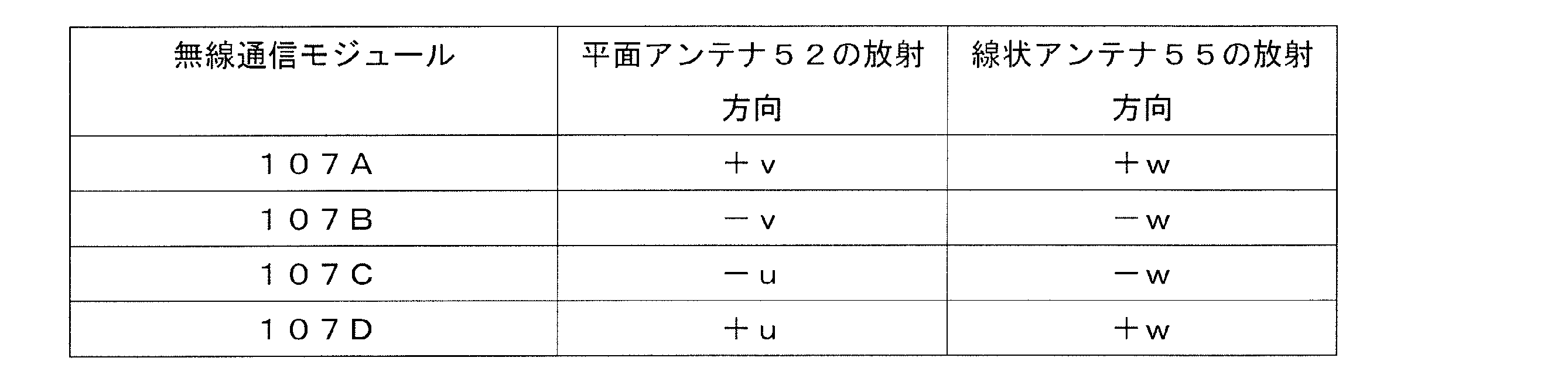
このように、図14に示す配置でも、無線通信装置110は、メインボード70に対して全方位(±u、±v、±w方向)へ電磁波を放射させることができる。
無線通信装置における無線通信モジュール107の配置は、上記実施形態に限られず、さらに種々の改変が可能である。例えば、複数の無線モジュールのうち一部は、メインボード70の主面70a、70bの少なくとも1つに配置し、残りの無線モジュールは、側部70c、70d、70e、70fの少なくとも1つに配置してもよい。
(その他の形態)
第1~第5の実施形態で説明した平面アレイアンテナ等の特徴は適宜組み合わせて実施することが可能である。例えば、共通地導体のy軸方向の幅がアンテナ地導体のy軸方向の最大幅よりも小さいという特徴は、第1~第5の実施形態の他の任意の実施形態と組み合わせることが可能である。また、平面アレイアンテナにおける平面アンテナの数も実施形態で示した値に限られない。平面アレイアンテナは例えば、x軸方向およびy軸方向の2次元に配置されていてもよい。また、平面状放射導体の形状も図示した形状に限られない。
第1~第5の実施形態で説明した平面アレイアンテナ等の特徴は適宜組み合わせて実施することが可能である。例えば、共通地導体のy軸方向の幅がアンテナ地導体のy軸方向の最大幅よりも小さいという特徴は、第1~第5の実施形態の他の任意の実施形態と組み合わせることが可能である。また、平面アレイアンテナにおける平面アンテナの数も実施形態で示した値に限られない。平面アレイアンテナは例えば、x軸方向およびy軸方向の2次元に配置されていてもよい。また、平面状放射導体の形状も図示した形状に限られない。
本開示の平面アンテナ、平面アレイアンテナ、多軸アレイアンテナ、無線通信モジュールおよび無線通信装置は、種々の高周波無線通信用のアンテナおよびアンテナを含む無線通信回路に好適に用いることが可能であり、特に準マイクロ波・センチメートル波・準ミリ波・ミリ波帯の無線通信装置に好適に用いられる。
11 平面状放射導体
12~15 無給電導体
12d~15d 辺
21 第1ストリップ導体
22 第2ストリップ導体
23 ビア導体
25、26 線状放射導体
27、28 給電導体
31、33 アンテナ地導体
31c、32c 孔
32 共通地導体
33a~33h 辺
40 誘電体
40a、40b 主面
40c~40f 側面
40h 誘電体40の部分
41 第1ビア導体
42 第2ビア導体
43 第3ビア導体
50、50’、52、52’ 平面アンテナ
55 線状アンテナ
60 アンテナユニット
61 導体
62 ビア導体
63 電極
64、65 能動素子
66 受動素子
67 コネクタ
68 カバー
69 可撓性配線
70 メインボード
70a、70b 主面
70c~70f 側部
71 封止樹脂
101から105 平面アレイアンテナ
106 多軸アレインテナ
107、107A~107D、108 無線通信モジュール
109、110 無線通信装置
Claims (21)
- 平面状放射導体と、
共通地導体と、
前記平面状放射導体と、前記共通地導体との間に位置し、第1、第2および第3軸を有する第1右手直交座標系において、第1軸に平行な方向に伸びる第1ストリップ導体と、
前記平面状放射導体と、前記共通地導体との間に位置し、前記第1ストリップ導体の伸びる方向と直交する方向に伸びる第2ストリップ導体と、
前記第1軸に対して45±3°または-45±3°の角度をなしており、前記平面状放射導体と対向している辺を有する少なくとも一対の無給電導体と、
を備えた、平面アンテナ。 - 前記第1軸に対して45±3°の角度をなしており、前記平面状放射導体と対向している辺を有する前記一対の無給電導体と、
前記第1軸に対して-45±3°の角度をなしており、前記平面状放射導体と対向している辺を有する他の一対の無給電導体と、
を備える請求項1に記載の平面アンテナ。 - 前記平面状放射導体と、前記無給電導体とは同一平面上に位置している請求項1または2に記載の平面アンテナ。
- 前記第1ストリップ導体および前記第2ストリップ導体と、前記共通地導体との間に位置するアンテナ地導体をさらに含み、前記アンテナ地導体は、前記第3軸方向からみて、少なくとも前記平面状放射導体全体と重なっている、請求項1から3のいずれかに記載の平面アンテナ。
- 前記無給電導体と前記アンテナ地導体とを接続する少なくとも1つの第1ビア導体をさらに備える請求項4に記載の平面アンテナ。
- 前記第3軸方向に垂直な主面を有する誘電体をさらに備え、
前記平面状放射導体、前記共通地導体、前記第1ストリップ導体、前記第2ストリップ導体および前記無給電導体は前記誘電体内に位置している、請求項5に記載の平面アンテナ。 - 前記第1軸方向に配列された、複数の請求項5に記載の平面アンテナを備え、
各平面アンテナの誘電体は一体的に構成されており、
各平面アンテナの共通地導体は互いに接続されており、
各平面アンテナのアンテナ地導体は、互いに分離している、平面アレイアンテナ。 - 前記複数の平面アンテナのうち、少なくとも1つの隣接する一対の平面アンテナにおいて、前記第3軸に沿って伸び、前記第2軸と平行に配列された複数の第2ビア導体を備え、
前記複数の第2ビア導体は、前記共通地導体と接続されている、請求項7に記載の平面アレイアンテナ。 - 前記複数の第2ビア導体は、前記隣接する一対の平面アンテナの一方のアンテナ地導体とさらに接続された第1グループと、前記隣接する一対の平面アンテナの他方のアンテナ地導体とさらに接続された第2グループとを含む請求項8に記載の平面アレイアンテナ。
- 前記複数の第2ビア導体は、前記第3軸と平行な方向において、前記共通地導体と前記平面状放射導体との距離以上の高さを有する請求項9に記載の平面アレイアンテナ。
- 平面状放射導体と、
共通地導体と、
前記平面状放射導体と、前記共通地導体との間に位置し、第1、第2および第3軸を有する第1右手直交座標系において、第1軸に対して45±3°の角度をなす方向に伸びる第1ストリップ導体と、
前記平面状放射導体と、前記共通地導体との間に位置し、前記第1ストリップ導体の伸びる方向と直交する方向に伸びる第2ストリップ導体と、
前記第1ストリップ導体および前記第2ストリップ導体と、前記共通地導体との間に位置し、前記第1軸に対して45±3°または-45±3°の角度をなす少なくとも一対の辺を外縁に有するアンテナ地導体と、
を備えた、平面アンテナ。 - 前記アンテナ地導体は、前記第3軸方向から見て、
前記第1軸に対して45±3°の角度をなしており、前記平面状放射導体を挟む前記一対の辺と、
前記第1軸に対して-45±3°の角度をなしており、前記平面状放射導体を挟む他の一対の辺と、
を備える請求項11に記載の平面アンテナ。 - 前記アンテナ地導体の前記外縁に沿って位置し、前記アンテナ地導体と前記共通地導体とを接続する少なくとも1つの第3ビア導体をさらに備える請求項11または12に記載の平面アンテナ。
- 前記共通地導体の前記第2軸に平行な方向の幅は、前記アンテナ地導体の前記第2軸に平行な最大幅よりも小さい、請求項11から13のいずれかに記載の平面アンテナ。
- 前記第3軸方向に垂直な主面を有する誘電体をさらに備え、
前記平面状放射導体、前記共通地導体、前記第1ストリップ導体、前記第2ストリップ導体および前記アンテナ地導体は前記誘電体内に位置している、請求項11から14のいずれかに記載の平面アンテナ。 - 前記第1軸方向に配列された、複数の請求項15に記載の平面アンテナを備え、
各平面アンテナの誘電体は一体的に構成されており、
各平面アンテナの共通地導体は互いに接続されており、
各平面アンテナのアンテナ地導体は互いに接続されている、平面アレイアンテナ。 - 前記複数の平面アンテナのうち、少なくとも1つの隣接する一対の平面アンテナにおいて、前記第3軸に沿って伸び、前記第2軸と平行に配列された複数の第2ビア導体を備え、
前記複数の第2ビア導体は、前記共通地導体と接続されている、請求項16に記載の平面アレイアンテナ。 - 請求項7から10、16および17のいずれかに記載の平面アレイアンテナと、
複数の線状アンテナと、
を備え、
各線状アンテナは、前記複数の平面アンテナの1つに対して、前記第2軸方向に離間して位置し、前記第1軸と平行に伸びる1つまたは2つの線状放射導体を含む、
多軸アレイアンテナ。 - 前記誘電体は、前記主面に隣接し、かつ、前記第2軸に垂直な側面を有し、
前記線状アンテナの前記1つまたは2つの線状放射導体は、前記側面に近接して前記誘電体内に配置されている、請求項18に記載の多軸アレイアンテナ。 - 請求項19に記載の多軸アレイアンテナと、
能動部品および受動部品からなる群から選ばれる少なくとも1つと
を備えた無線通信モジュール。 - 第1、第2および第3軸を有する第2右手直交座標系において、第3軸に垂直な第1および第2主面と、前記第1軸に垂直な第1および第2側部と、前記第2軸に垂直な第3および第4側部と、送信回路および受信回路の少なくとも一方とを有する回路基板と、
少なくとも1つの請求項20に記載の無線通信モジュールと、
を備え、
前記少なくとも1つの無線通信モジュールは、前記第1および第2主面、前記第1、第2、第3および第4側部の少なくとも1つに配置されている、無線通信装置。
Priority Applications (3)
| Application Number | Priority Date | Filing Date | Title |
|---|---|---|---|
| JP2020569691A JP7067641B2 (ja) | 2019-01-31 | 2020-01-29 | 平面アンテナ、平面アレイアンテナ、多軸アレイアンテナ、無線通信モジュールおよび無線通信装置 |
| CN202080011598.8A CN113366704B (zh) | 2019-01-31 | 2020-01-29 | 平面天线、平面阵列天线、多轴阵列天线、无线通信模块和无线通信装置 |
| US17/386,894 US11888240B2 (en) | 2019-01-31 | 2021-07-28 | Planar antenna, planar array antenna, multi-axis array antenna, and wireless communication module |
Applications Claiming Priority (2)
| Application Number | Priority Date | Filing Date | Title |
|---|---|---|---|
| JP2019-015994 | 2019-01-31 | ||
| JP2019015994 | 2019-01-31 |
Related Child Applications (1)
| Application Number | Title | Priority Date | Filing Date |
|---|---|---|---|
| US17/386,894 Continuation US11888240B2 (en) | 2019-01-31 | 2021-07-28 | Planar antenna, planar array antenna, multi-axis array antenna, and wireless communication module |
Publications (1)
| Publication Number | Publication Date |
|---|---|
| WO2020158810A1 true WO2020158810A1 (ja) | 2020-08-06 |
Family
ID=71840185
Family Applications (1)
| Application Number | Title | Priority Date | Filing Date |
|---|---|---|---|
| PCT/JP2020/003194 Ceased WO2020158810A1 (ja) | 2019-01-31 | 2020-01-29 | 平面アンテナ、平面アレイアンテナ、多軸アレイアンテナ、無線通信モジュールおよび無線通信装置 |
Country Status (4)
| Country | Link |
|---|---|
| US (1) | US11888240B2 (ja) |
| JP (1) | JP7067641B2 (ja) |
| CN (1) | CN113366704B (ja) |
| WO (1) | WO2020158810A1 (ja) |
Cited By (5)
| Publication number | Priority date | Publication date | Assignee | Title |
|---|---|---|---|---|
| WO2022181470A1 (ja) * | 2021-02-26 | 2022-09-01 | 京セラ株式会社 | 円偏波アレイアンテナ及び電子機器 |
| JPWO2022264415A1 (ja) * | 2021-06-18 | 2022-12-22 | ||
| JP2024002957A (ja) * | 2022-06-24 | 2024-01-11 | トロン フューチャー テック インコーポレイテッド | フェーズドアレイアンテナ用の無線周波数回路 |
| JP7514293B1 (ja) | 2022-12-29 | 2024-07-10 | 電気興業株式会社 | フェーズドアレー用アンテナ素子およびフェーズドアレーアンテナ |
| JP2025087665A (ja) * | 2023-11-29 | 2025-06-10 | 群▲マイ▼通訊股▲ふん▼有限公司 | アレイアンテナモジュール及び無線通信装置 |
Families Citing this family (9)
| Publication number | Priority date | Publication date | Assignee | Title |
|---|---|---|---|---|
| US11402465B2 (en) * | 2019-04-05 | 2022-08-02 | Samsung Electronics Co., Ltd. | Radar leakage cancelation based on spatiotemporal relationship of transmit and receive antenna pairs |
| WO2020212819A1 (en) * | 2019-04-15 | 2020-10-22 | Telefonaktiebolaget Lm Ericsson (Publ) | Integrated antenna and filter unit (iafu) for 5th generation advanced antenna system (aas) systems |
| US12401117B2 (en) * | 2019-12-26 | 2025-08-26 | Telefonaktiebolaget Lm Ericsson (Publ) | Antenna unit, antenna module and base station having the same |
| US12586883B2 (en) | 2020-09-29 | 2026-03-24 | Telefonaktiebolaget Lm Ericsson (Publ) | Filter unit, antenna filter unit and radio unit |
| JP7764226B2 (ja) * | 2021-12-06 | 2025-11-05 | 日本航空電子工業株式会社 | アンテナ装置 |
| CN114566804B (zh) * | 2022-03-17 | 2025-08-15 | 广东分数维无线科技有限公司 | 一种宽频带毫米波电调寄生天线 |
| US12149008B2 (en) * | 2022-08-19 | 2024-11-19 | Google Llc | Low-footprint dual-band ultra-wideband antenna modules |
| US12211773B2 (en) * | 2022-09-15 | 2025-01-28 | JCET STATS ChipPAC Korea Limited | Integrated antenna-in-package structure |
| CN117954843B (zh) * | 2024-03-26 | 2024-09-06 | 隔空(上海)智能科技有限公司 | 一种毫米波雷达射频前端模组 |
Citations (3)
| Publication number | Priority date | Publication date | Assignee | Title |
|---|---|---|---|---|
| JPH0270104A (ja) * | 1988-06-14 | 1990-03-09 | Koden Electron Co Ltd | 広指向性マイクロストリップアンテナ |
| JP2002033619A (ja) * | 2000-07-18 | 2002-01-31 | Hitachi Cable Ltd | アンテナ装置 |
| WO2014073355A1 (ja) * | 2012-11-07 | 2014-05-15 | 株式会社村田製作所 | アレーアンテナ |
Family Cites Families (18)
| Publication number | Priority date | Publication date | Assignee | Title |
|---|---|---|---|---|
| EP1526604A1 (en) * | 1999-09-20 | 2005-04-27 | Fractus, S.A. | Multilevel antenna |
| US6650299B2 (en) | 2000-07-18 | 2003-11-18 | Hitachi Cable, Ltd. | Antenna apparatus |
| CN2593385Y (zh) * | 2002-12-10 | 2003-12-17 | 烟台高盈科技有限公司 | 一种四探针扇形波束基站用天线 |
| CN2703335Y (zh) * | 2004-05-18 | 2005-06-01 | 摩比天线技术(深圳)有限公司 | 一种空气微带耦合馈电贴片天线 |
| JP4789532B2 (ja) * | 2004-09-27 | 2011-10-12 | 日本無線株式会社 | 円偏波パッチアンテナ及び円偏波アレイアンテナ |
| DE102005010894B4 (de) * | 2005-03-09 | 2008-06-12 | Fraunhofer-Gesellschaft zur Förderung der angewandten Forschung e.V. | Planare Mehrbandantenne |
| JP2011055036A (ja) * | 2009-08-31 | 2011-03-17 | Kumamoto Univ | 平面アンテナおよび平面アンテナの偏波方式 |
| CN108550986A (zh) * | 2012-09-21 | 2018-09-18 | 株式会社村田制作所 | 双极化天线 |
| CN102842756B (zh) * | 2012-09-24 | 2015-07-22 | 桂林电子科技大学 | 双极化mimo天线阵 |
| CN103490151B (zh) * | 2013-08-30 | 2015-08-26 | 大连海事大学 | 一种l波段宽频带圆极化微带天线 |
| JP6117833B2 (ja) | 2015-02-09 | 2017-04-19 | Necプラットフォームズ株式会社 | ダイバーシティアンテナ装置 |
| CN204441474U (zh) * | 2015-02-13 | 2015-07-01 | 安弗施无线射频系统(上海)有限公司 | 辐射单元及双极化天线 |
| CN106159436A (zh) * | 2015-04-24 | 2016-11-23 | 桂林嘉威信息技术有限公司 | 一种适用于wlan的小型化双极化天线及其制作方法 |
| DE112016005738T5 (de) * | 2015-12-15 | 2018-10-04 | Denso Corporation | Antennenvorrichtung |
| JP6499116B2 (ja) * | 2016-04-06 | 2019-04-10 | 株式会社Soken | アンテナ装置 |
| US20190245275A1 (en) * | 2016-07-29 | 2019-08-08 | Hitachi Metals, Ltd. | Planar array antenna and quasi-millimeter wave/millimeter wave wireless communication module |
| CN106299668B (zh) * | 2016-09-27 | 2023-06-16 | 华南理工大学 | 一种差分馈电宽带双极化平面基站天线 |
| CN107768828B (zh) * | 2017-11-21 | 2023-08-08 | 广东通宇通讯股份有限公司 | 天线安装结构件及其引向器 |
-
2020
- 2020-01-29 JP JP2020569691A patent/JP7067641B2/ja active Active
- 2020-01-29 CN CN202080011598.8A patent/CN113366704B/zh active Active
- 2020-01-29 WO PCT/JP2020/003194 patent/WO2020158810A1/ja not_active Ceased
-
2021
- 2021-07-28 US US17/386,894 patent/US11888240B2/en active Active
Patent Citations (3)
| Publication number | Priority date | Publication date | Assignee | Title |
|---|---|---|---|---|
| JPH0270104A (ja) * | 1988-06-14 | 1990-03-09 | Koden Electron Co Ltd | 広指向性マイクロストリップアンテナ |
| JP2002033619A (ja) * | 2000-07-18 | 2002-01-31 | Hitachi Cable Ltd | アンテナ装置 |
| WO2014073355A1 (ja) * | 2012-11-07 | 2014-05-15 | 株式会社村田製作所 | アレーアンテナ |
Cited By (12)
| Publication number | Priority date | Publication date | Assignee | Title |
|---|---|---|---|---|
| WO2022181470A1 (ja) * | 2021-02-26 | 2022-09-01 | 京セラ株式会社 | 円偏波アレイアンテナ及び電子機器 |
| JPWO2022181470A1 (ja) * | 2021-02-26 | 2022-09-01 | ||
| JP7577187B2 (ja) | 2021-02-26 | 2024-11-01 | 京セラ株式会社 | 円偏波アレイアンテナ及び電子機器 |
| JPWO2022264415A1 (ja) * | 2021-06-18 | 2022-12-22 | ||
| WO2022264415A1 (ja) * | 2021-06-18 | 2022-12-22 | Fcnt株式会社 | アンテナ装置及び無線通信装置 |
| JP7698717B2 (ja) | 2021-06-18 | 2025-06-25 | Fcnt合同会社 | アンテナ装置及び無線通信装置 |
| JP2024002957A (ja) * | 2022-06-24 | 2024-01-11 | トロン フューチャー テック インコーポレイテッド | フェーズドアレイアンテナ用の無線周波数回路 |
| JP7599235B2 (ja) | 2022-06-24 | 2024-12-13 | トロン フューチャー テック インコーポレイテッド | フェーズドアレイアンテナ用の無線周波数回路 |
| US12543259B2 (en) | 2022-06-24 | 2026-02-03 | Tron Future Tech Inc. | Radio-frequency circuit for phased array antenna |
| JP7514293B1 (ja) | 2022-12-29 | 2024-07-10 | 電気興業株式会社 | フェーズドアレー用アンテナ素子およびフェーズドアレーアンテナ |
| JP2024097354A (ja) * | 2022-12-29 | 2024-07-19 | 電気興業株式会社 | フェーズドアレー用アンテナ素子およびフェーズドアレーアンテナ |
| JP2025087665A (ja) * | 2023-11-29 | 2025-06-10 | 群▲マイ▼通訊股▲ふん▼有限公司 | アレイアンテナモジュール及び無線通信装置 |
Also Published As
| Publication number | Publication date |
|---|---|
| US11888240B2 (en) | 2024-01-30 |
| JPWO2020158810A1 (ja) | 2021-11-25 |
| JP7067641B2 (ja) | 2022-05-16 |
| US20210359415A1 (en) | 2021-11-18 |
| CN113366704A (zh) | 2021-09-07 |
| CN113366704B (zh) | 2023-08-01 |
Similar Documents
| Publication | Publication Date | Title |
|---|---|---|
| JP7067641B2 (ja) | 平面アンテナ、平面アレイアンテナ、多軸アレイアンテナ、無線通信モジュールおよび無線通信装置 | |
| CN112350051B (zh) | 多频段天线和多频段天线的设计方法 | |
| US11011843B2 (en) | Antenna element, antenna module, and communication apparatus | |
| US10950945B2 (en) | Antenna element, antenna module, and communication apparatus | |
| WO2019026913A1 (ja) | 多軸アンテナ、無線通信モジュールおよび無線通信装置 | |
| JP6579298B1 (ja) | マルチバンドアンテナ、無線通信モジュールおよび無線通信装置 | |
| JP6747591B2 (ja) | 平面アレイアンテナおよび無線通信モジュール | |
| US20070013599A1 (en) | Apparatus and methods for constructing and packaging printed antenna devices | |
| US12283761B2 (en) | Antenna module and communication device including the same | |
| US11063363B2 (en) | Antenna element, antenna module, and communication device | |
| US20230411870A1 (en) | Antenna module and communication apparatus equipped with the same | |
| WO2019102988A1 (ja) | 平面アレイアンテナおよび無線通信モジュール | |
| US12381327B2 (en) | Antenna module and communication device including the same | |
| CN114284738B (zh) | 天线结构和天线封装 | |
| WO2020066604A1 (ja) | アンテナモジュール、通信装置およびアレイアンテナ | |
| JP4535640B2 (ja) | 開口面アンテナおよび開口面アンテナ付き基板 | |
| US20250015500A1 (en) | Antenna module and communication apparatus including the same | |
| US20240291166A1 (en) | Antenna module and communication apparatus including the same | |
| US12620711B2 (en) | Antenna module | |
| US20250239760A1 (en) | Antenna substrate and antenna module | |
| JP7577187B2 (ja) | 円偏波アレイアンテナ及び電子機器 | |
| JP2025111092A (ja) | アンテナモジュール | |
| KR20260027935A (ko) | 안테나 소자, 안테나 어레이 및 안테나 모듈 | |
| WO2025105188A1 (ja) | ミリ波無線通信装置 |
Legal Events
| Date | Code | Title | Description |
|---|---|---|---|
| 121 | Ep: the epo has been informed by wipo that ep was designated in this application |
Ref document number: 20748432 Country of ref document: EP Kind code of ref document: A1 |
|
| ENP | Entry into the national phase |
Ref document number: 2020569691 Country of ref document: JP Kind code of ref document: A |
|
| NENP | Non-entry into the national phase |
Ref country code: DE |
|
| 122 | Ep: pct application non-entry in european phase |
Ref document number: 20748432 Country of ref document: EP Kind code of ref document: A1 |