WO2020153079A1 - セラミックヒータ - Google Patents
セラミックヒータ Download PDFInfo
- Publication number
- WO2020153079A1 WO2020153079A1 PCT/JP2019/050428 JP2019050428W WO2020153079A1 WO 2020153079 A1 WO2020153079 A1 WO 2020153079A1 JP 2019050428 W JP2019050428 W JP 2019050428W WO 2020153079 A1 WO2020153079 A1 WO 2020153079A1
- Authority
- WO
- WIPO (PCT)
- Prior art keywords
- resistance heating
- heating element
- ceramic plate
- ceramic
- ceramic heater
- Prior art date
- Legal status (The legal status is an assumption and is not a legal conclusion. Google has not performed a legal analysis and makes no representation as to the accuracy of the status listed.)
- Ceased
Links
Images

Classifications
-
- H—ELECTRICITY
- H05—ELECTRIC TECHNIQUES NOT OTHERWISE PROVIDED FOR
- H05B—ELECTRIC HEATING; ELECTRIC LIGHT SOURCES NOT OTHERWISE PROVIDED FOR; CIRCUIT ARRANGEMENTS FOR ELECTRIC LIGHT SOURCES, IN GENERAL
- H05B3/00—Ohmic-resistance heating
- H05B3/68—Heating arrangements specially adapted for cooking plates or analogous hot-plates
- H05B3/74—Non-metallic plates, e.g. vitroceramic, ceramic or glassceramic hobs, also including power or control circuits
-
- H—ELECTRICITY
- H05—ELECTRIC TECHNIQUES NOT OTHERWISE PROVIDED FOR
- H05B—ELECTRIC HEATING; ELECTRIC LIGHT SOURCES NOT OTHERWISE PROVIDED FOR; CIRCUIT ARRANGEMENTS FOR ELECTRIC LIGHT SOURCES, IN GENERAL
- H05B3/00—Ohmic-resistance heating
- H05B3/20—Heating elements having extended surface area substantially in a two-dimensional [2D] plane, e.g. plate-heater
- H05B3/22—Heating elements having extended surface area substantially in a two-dimensional [2D] plane, e.g. plate-heater non-flexible
- H05B3/26—Heating elements having extended surface area substantially in a two-dimensional [2D] plane, e.g. plate-heater non-flexible heating conductor mounted on insulating base
- H05B3/265—Heating elements having extended surface area substantially in a two-dimensional [2D] plane, e.g. plate-heater non-flexible heating conductor mounted on insulating base the insulating base being an inorganic material, e.g. ceramic
-
- H—ELECTRICITY
- H10—SEMICONDUCTOR DEVICES; ELECTRIC SOLID-STATE DEVICES NOT OTHERWISE PROVIDED FOR
- H10P—GENERIC PROCESSES OR APPARATUS FOR THE MANUFACTURE OR TREATMENT OF DEVICES COVERED BY CLASS H10
- H10P72/00—Handling or holding of wafers, substrates or devices during manufacture or treatment thereof
- H10P72/04—Apparatus for manufacture or treatment
- H10P72/0431—Apparatus for thermal treatment
- H10P72/0432—Apparatus for thermal treatment mainly by conduction
-
- H—ELECTRICITY
- H05—ELECTRIC TECHNIQUES NOT OTHERWISE PROVIDED FOR
- H05B—ELECTRIC HEATING; ELECTRIC LIGHT SOURCES NOT OTHERWISE PROVIDED FOR; CIRCUIT ARRANGEMENTS FOR ELECTRIC LIGHT SOURCES, IN GENERAL
- H05B3/00—Ohmic-resistance heating
- H05B3/20—Heating elements having extended surface area substantially in a two-dimensional [2D] plane, e.g. plate-heater
- H05B3/22—Heating elements having extended surface area substantially in a two-dimensional [2D] plane, e.g. plate-heater non-flexible
- H05B3/28—Heating elements having extended surface area substantially in a two-dimensional [2D] plane, e.g. plate-heater non-flexible heating conductor embedded in insulating material
- H05B3/283—Heating elements having extended surface area substantially in a two-dimensional [2D] plane, e.g. plate-heater non-flexible heating conductor embedded in insulating material the insulating material being an inorganic material, e.g. ceramic
-
- H—ELECTRICITY
- H10—SEMICONDUCTOR DEVICES; ELECTRIC SOLID-STATE DEVICES NOT OTHERWISE PROVIDED FOR
- H10P—GENERIC PROCESSES OR APPARATUS FOR THE MANUFACTURE OR TREATMENT OF DEVICES COVERED BY CLASS H10
- H10P95/00—Generic processes or apparatus for manufacture or treatments not covered by the other groups of this subclass
Definitions
- the present invention relates to a ceramic heater.
- ⁇ Semiconductor manufacturing equipment uses ceramic heaters to heat wafers.
- a so-called two-zone heater is known as such a ceramic heater.
- As a two-zone heater of this type as disclosed in Patent Document 1, an inner peripheral resistance heating element and an outer peripheral resistance heating element are embedded in the same plane in a ceramic substrate, and It is known that the heat generated from each resistance heating element is independently controlled by independently applying a voltage.
- Each resistance heating element is a coil made of a refractory metal such as tungsten.
- each resistance heating element is a coil, it is necessary to provide an interval so that adjacent coils do not short-circuit. Further, although the ceramic heater is provided with gas holes and lift pin holes that penetrate the ceramic plate in the vertical direction, each resistance heating element needs to bypass these holes. Therefore, there is a problem that sufficient soaking property cannot be obtained.
- the present invention has been made in order to solve such a problem, and its main purpose is to obtain sufficient heat uniformity even when a coil is used as a main resistance heating element.
- the ceramic heater of the present invention is A ceramic plate having a wafer mounting surface, A coil-shaped main resistance heating element provided inside a first surface parallel to the wafer mounting surface inside the ceramic plate; A two-dimensional auxiliary resistance heating element which is provided inside the ceramic plate on a second surface parallel to the first surface and complements heating by the main resistance heating element; It is equipped with.
- the coil-shaped main resistance heating element provided inside the ceramic plate heats the wafer mounted on the wafer mounting surface. Since the main resistance heating element is a coil, there are restrictions on wiring. Therefore, it is difficult to finely adjust the temperature only by heating with the main resistance heating element.
- the two-dimensional auxiliary resistance heating element is provided on the second surface parallel to the first surface on which the main resistance heating element is provided inside the ceramic plate. Since this auxiliary resistance heating element has a two-dimensional shape, it can be manufactured by printing, and wiring with a high degree of freedom (for example, wiring with high density by narrowing the line width or narrowing the space between lines) is possible. It will be possible. Therefore, the sub resistance heating element can finely adjust the temperature by supplementing the heating by the coiled main resistance heating element. Therefore, even if a coil is used as the main resistance heating element, sufficient heat uniformity can be obtained.
- main resistance heating element and the sub resistance heating element may be made of the same material or different materials.
- parallel includes not only the case of being completely parallel but also the case of being substantially parallel (for example, within a tolerance range).
- the second surface may be located between the first surface and the wafer mounting surface.
- the sub resistance heating element may contain a ceramic.
- the thermal expansion coefficient of the auxiliary resistance heating element can be made close to the thermal expansion coefficient of the ceramic plate, and the bonding strength between the auxiliary resistance heating element and the ceramic plate can be increased.
- the main resistance heating element is provided in each of m (m is an integer of 1 or more) zones in the first surface, and the sub resistance heating element is provided in the second surface. May be provided in each of the n zones (n is an integer larger than m).
- the temperature can be adjusted individually for each zone, and thus it is easy to finely adjust the temperature of the wafer mounting surface.
- the auxiliary resistance heating element suitable for fine adjustment of the temperature is provided in each of the zones of the second surface which is divided into more zones than the first surface, the temperature of the wafer mounting surface is finely adjusted. It's easy to do.
- the sub resistance heating element may be divided into a fan shape. This makes it possible to improve the thermal uniformity of the ceramic plate in the circumferential direction, and more precise temperature control becomes possible.
- the sub resistance heating element may be closer to the hole than the main resistance heating element.
- the sub resistance heating element may be arranged at a position overlapping the terminal of the main resistance heating element when the wafer mounting surface is viewed in plan. This makes it possible to finely adjust the temperature by supplementing the area immediately above the terminal of the main resistance heating element, which tends to be low temperature, with the heating by the sub resistance heating element.
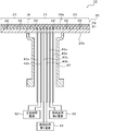
- FIG. 3 is a vertical sectional view of the ceramic heater 10. Sectional drawing when the ceramic plate 20 is cut
- FIG. 1 is a perspective view of a ceramic heater 10 of the present embodiment
- FIG. 2 is a vertical sectional view of the ceramic heater 10 (a sectional view when the ceramic heater 10 is cut along a plane including a central axis).
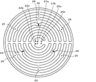
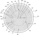
- 3 is a cross-sectional view of the ceramic plate 20 taken along the first surface P1 and viewed from above
- FIG. 4 is a cross-sectional view of the ceramic plate 20 taken along the second surface P2 and viewed from above.
- hatching showing the cut surface is omitted.
- the ceramic heater 10 is used to heat a wafer to be subjected to processing such as etching and CVD, and is installed in a vacuum chamber (not shown).
- the ceramic heater 10 has a disk-shaped ceramic plate 20 having a wafer mounting surface 20a, and a ceramic plate 20 coaxial with the ceramic plate 20 on a surface (back surface) 20b of the ceramic plate 20 opposite to the wafer mounting surface 20a. And a tubular shaft 40 joined together.
- the ceramic plate 20 is a disc-shaped plate made of a ceramic material typified by aluminum nitride or alumina.
- the diameter of the ceramic plate 20 is, for example, about 300 mm.
- the wafer mounting surface 20a of the ceramic plate 20 is provided with fine irregularities (not shown) by embossing.
- the ceramic plate 20 has a virtual first surface P1 parallel to the wafer mounting surface 20a and a virtual second surface P2 parallel to the first surface P1.
- the second surface P2 is between the first surface P1 and the wafer mounting surface 20a.
- the second surface P2 of the ceramic plate 20 is divided into a small circular inner peripheral side zone Z1 and an annular outer peripheral side zone Z2 by an imaginary boundary 20c concentric with the ceramic plate 20 (see FIG. 4).
- the diameter of the virtual boundary 20c is, for example, about 200 mm.
- a main resistance heating element 22 is provided on the first surface P1 of the ceramic plate 20.
- the inner peripheral side auxiliary resistance heating element 23 is provided in the inner peripheral side zone Z1
- the outer peripheral side auxiliary resistance heating element 25 is provided in the outer peripheral side zone Z2.
- the main resistance heating element 22 and the sub resistance heating elements 23 and 25 are embedded in the ceramic plate 20.
- the ceramic plate 20 is provided with a plurality of gas holes 26 as shown in FIGS.
- the gas hole 26 penetrates from the back surface 20b of the ceramic plate 20 to the wafer mounting surface 20a, and between the unevenness provided on the wafer mounting surface 20a and the wafer W mounted on the wafer mounting surface 20a.
- the gas is supplied to the resulting gap.
- the gas supplied to this gap serves to improve the heat conduction between the wafer mounting surface 20a and the wafer W.
- the ceramic plate 20 has a plurality of lift pin holes 28.
- the lift pin hole 28 penetrates from the back surface 20b of the ceramic plate 20 to the wafer mounting surface 20a, and a lift pin (not shown) is inserted therein.
- the lift pins serve to lift the wafer W mounted on the wafer mounting surface 20a.
- a plurality of lift pin holes 28 (here, three) are provided at equal intervals on the same circumference.
- the main resistance heating element 22 includes a pair of terminals 22a and 22b arranged in the central portion of the ceramic plate 20 (a region of the back surface 20b of the ceramic plate 20 surrounded by the cylindrical shaft 40). It is formed so as to start from one end, be folded back at a plurality of folding parts in a one-stroke manner, and be wired over almost the entire area of the first surface P1 and then reach the other of the pair of terminals 22a, 22b.
- the main resistance heating element 22 has a curved portion 22p that bypasses the gas hole 26 and the lift pin hole 28.
- the main resistance heating element 22 is a coil whose main component is a high melting point metal or its carbide.
- Examples of the high melting point metal include tungsten, molybdenum, tantalum, platinum, rhenium, hafnium and alloys thereof.
- Examples of the carbide of the high melting point metal include tungsten carbide and molybdenum carbide. Since the main resistance heating element 22 is a coil, the space between adjacent coils is set wider so as not to short circuit.
- the inner peripheral side auxiliary resistance heating element 23 originates from one of the pair of terminals 23a and 23b arranged in the central portion of the ceramic plate 20, and has a plurality of folded portions in a one-stroke manner. It is formed so as to reach the other of the pair of terminals 23a and 23b after being wired in the entire area of the inner peripheral side zone Z1 while being folded back at.
- the inner peripheral side auxiliary resistance heating element 23 is arranged at a position overlapping the terminals 22a and 22b of the main resistance heating element 22 when the wafer mounting surface 20a is viewed in a plan view. As shown in FIG.
- the outer peripheral side resistance heating element 25 originates from one of the pair of terminals 25a and 25b arranged in the central portion of the ceramic plate 20, and is folded back at a plurality of folding portions in a single stroke. It is formed so as to reach almost the entire area of the outer peripheral side zone Z2 and reach the other of the pair of terminals 25a and 25b.
- the inner peripheral side auxiliary resistance heating element 23 and the outer peripheral side auxiliary resistance heating element 25 are ribbons (flat and elongated shape) of refractory metal or its carbide, and are formed by printing a paste of refractory metal or its carbide. ing. Therefore, the sub resistance heating elements 23 and 25 can be wired with a high degree of freedom.
- the line width of the ribbons of the auxiliary resistance heating elements 23 and 25 is formed smaller than the coil diameter of the main resistance heating element 22.
- the adjacent ribbons of the sub resistance heating elements 23 and 25 are arranged such that the interval between adjacent ribbons is smaller than the interval between adjacent coils of the main resistance heating element 22.
- the interval between the portions where the folded-back portions 23c face each other and the portions where the folded-back portions 25c face each other is the same as the portion where the folded-back portions 22c of the main resistance heating body 22 face each other.
- the wiring is narrower than the space.
- the auxiliary resistance heating elements 23 and 25 are wired closer to the gas holes 26 and the lift pin holes 28 than the main resistance heating elements 22.
- the tubular shaft 40 is made of a ceramic such as aluminum nitride or alumina, like the ceramic plate 20.
- the cylindrical shaft has an inner diameter of, for example, about 40 mm and an outer diameter of, for example, about 60 mm.
- the upper end of the tubular shaft 40 is diffusion bonded to the ceramic plate 20.
- power supply rods 42 a and 42 b connected to the pair of terminals 22 a and 22 b of the main resistance heating element 22 are arranged inside the cylindrical shaft 40.
- the power supply rods 43 a and 43 b connected to the pair of terminals 23 a and 23 b of the inner peripheral side auxiliary resistance heating element 23 and the pair of terminals of the outer peripheral side auxiliary resistance heating element 25, respectively.
- Power supply rods 45a and 45b connected to each of 25a and 25b are arranged.
- the power supply rods 42a and 42b are connected to the main resistance power supply 32
- the power supply rods 43a and 43b are connected to the sub resistance first power supply 33
- the power supply rods 45a and 45b are connected to the sub resistance second power supply 35.
- a gas supply pipe for supplying gas to the gas hole 26 and a lift pin inserted into the lift pin hole 28 are also arranged inside the tubular shaft 40.
- the ceramic heater 10 is installed in a vacuum chamber (not shown), and the wafer W is mounted on the wafer mounting surface 20a of the ceramic heater 10. Then, the temperature of the inner peripheral side zone Z1 detected by the inner peripheral side thermocouple (not shown) becomes a predetermined inner peripheral side target temperature, and the temperature of the outer peripheral side zone Z2 detected by the outer peripheral side thermocouple (not shown).
- the electric power supplied to the resistance heating elements 22, 23, 25 is adjusted by the power sources 32, 33, 35 so that the temperature becomes a predetermined outer peripheral side target temperature. As a result, the temperature of the wafer W is controlled to a desired temperature.
- the main resistance heating element 22 is formed of a coil, it is used to roughly control the temperatures of the zones Z1 and Z2 to the target temperatures. Further, since the inner peripheral side and outer peripheral side auxiliary resistance heating elements 23 and 25 are formed by ribbons arranged at higher density than the coils, the temperature of each zone Z1 and Z2 is adjusted so as to reach each target temperature. Used to adjust.
- the inside of the vacuum chamber is set to a vacuum atmosphere or a reduced pressure atmosphere, plasma is generated in the vacuum chamber, and the wafer W is subjected to CVD film formation or etching using the plasma.
- the auxiliary resistance heating elements 23 and 25 are ribbon-shaped, they can be manufactured by printing, the line width and the line spacing can be reduced, and the degree of freedom is high. Wiring is possible. Therefore, the auxiliary resistance heating elements 23 and 25 can finely adjust the temperature by supplementing the heating by the coiled main resistance heating element 22. Therefore, even when a coil is used as the main resistance heating element 22, sufficient heat uniformity can be obtained.
- the main resistance heating element 22 is a coil
- the coil may be embedded in ceramic powder and then fired. In that case, since the coil may move in the ceramic powder, it is necessary to wire the coil in consideration of it. Therefore, for example, in the main resistance heating element 22, it is necessary to wire the gap between adjacent coils and the gap between portions where the folded portions 22c face each other relatively widely. Further, for example, the main resistance heating element 22 needs to be routed around the gas hole 26 and the lift pin hole 28. Therefore, the temperature tends to be lower than the other portions in the portions between the adjacent coils, the portions where the folded portions 22c face each other, the holes 26, 28 and the like, and it is difficult to finely adjust the temperature.
- the sub resistance heating elements 23 and 25, which are ribbons having a higher degree of freedom in wiring than the coil, are wired so that the distance between the sub resistance heating elements 23 and 25 is narrower than that of the main resistance heating element 22, and the wiring is provided near the holes 26 and 28. There is. Therefore, the temperature can be finely adjusted by, for example, supplementing the portion where the temperature is likely to be lowered by the heating by the main resistance heating element 22 with the heating by the sub resistance heating elements 23 and 25.
- the distance between the coils is usually about 1 mm.
- the distance between the ribbons can be set to about 0.3 mm because the ribbons can be produced by printing.
- the main resistance heating element 22 and the sub resistance heating elements 23 and 25 are provided on different surfaces P1 and P2 of the inside of the ceramic plate, respectively, the sub resistance is less than when they are provided on the same surface.
- the degree of freedom of wiring of the heating elements 23 and 25 can be further increased. Therefore, it is easy to finely adjust the temperature of the wafer mounting surface 20a.
- the main resistance heating element 22 is a coil-shaped resistance heating element that generally generates a larger amount of heat than the ribbon-shaped resistance heating element, and the sub-resistance heating elements 23 and 25 are more than the coil-shaped resistance heating element. Is also a thin ribbon-shaped resistance heating element.
- the thickness of the resistance heating element can be made thinner than that in the case where both are coil-shaped, and thus the thickness of the ceramic plate 20 can be made thinner. Further, it is easier to increase the amount of heat generation than when both are ribbon-shaped, and it is suitable for raising the temperature of the ceramic heater 10.
- the second surface P2 provided with the sub resistance heating elements 23 and 25 is between the first surface P1 provided with the main resistance heating element 22 and the wafer mounting surface 20a, the sub resistance heating element is provided.
- the heating by 23 and 25 is likely to be reflected in the temperature of the wafer mounting surface 20a. Therefore, it is easy to finely adjust the temperature of the wafer mounting surface 20a.
- the auxiliary resistance heating elements 23 and 25 are provided in each of the two zones Z1 and Z2 in the second surface P2, the temperature can be adjusted individually for each zone. Particularly, since the auxiliary resistance heating elements 23 and 25 suitable for fine adjustment of the temperature are provided in the zones Z1 and Z2 of the second surface P2, which are divided into more zones than the first surface P1, respectively, the wafer It is easy to finely adjust the temperature of the mounting surface 20a. Since the auxiliary resistance heating elements 23 and 25 have high wiring flexibility, they are suitable for multiple zones.
- the inner peripheral side auxiliary resistance heating element 23 is arranged at a position overlapping the terminals 22a and 22b of the main resistance heating element 22 when the wafer mounting surface 20a is viewed in a plan view, the main resistance heating which tends to be low in temperature is generated. It is possible to finely adjust the temperature by supplementing the area immediately above the terminals 22a and 22b of the body 22 with the heating by the inner peripheral side auxiliary resistance heating element 23.
- the auxiliary resistance heating elements 23 and 25 are ribbons, but the present invention is not limited to this, and any shape may be adopted as long as it is a two-dimensional shape. Since the two-dimensional shape can be produced by printing a paste, the auxiliary resistance heating elements 23 and 25 can be easily thinned and can be wired at a high density.
- the auxiliary resistance heating elements 23 and 25 of the above-described embodiment may contain ceramics.
- the paste for forming the auxiliary resistance heating elements 23 and 25 by printing may contain ceramics.
- the second surface P2 is between the first surface P1 and the wafer mounting surface 20a, but the second surface P2 is between the first surface P1 and the back surface 20b of the ceramic plate 20. May be.
- the interval between the ribbons of the sub resistance heating elements 23 and 25 is made narrower than the interval between the coils of the main resistance heating element 22, but the main resistance heating element 22 is heated by the sub resistance heating elements 23 and 25.
- Any wiring may be used as long as it can supplement the heating by.
- the spacing between the ribbons of the sub resistance heating elements 23 and 25 is set to be approximately the same as the spacing between the coils of the main resistance heating element 22, and the sub resistance heating element is provided at a portion corresponding to the coil between the main resistance heating elements 22. You may wire 23 and 25.
- the line width of the ribbons of the auxiliary resistance heating elements 23 and 25 is smaller than the coil diameter of the main resistance heating element 22, but may be equal to or larger than the coil diameter of the main resistance heating element 22.
- the ceramic plate 20 may have an electrostatic electrode built therein.
- the wafer W can be electrostatically attracted to the wafer mounting surface 20a by applying a voltage to the electrostatic electrode after mounting the wafer W on the wafer mounting surface 20a.
- the ceramic plate 20 may have an RF electrode built therein.
- a shower head (not shown) is arranged above the wafer mounting surface 20a with a space provided, and high-frequency power is supplied between the parallel plate electrodes including the shower head and the RF electrodes. By doing so, plasma can be generated and the wafer W can be subjected to CVD film formation or etching using the plasma.
- the electrostatic electrode may also be used as the RF electrode.
- the outer peripheral side zone Z2 of the second surface P2 has been described as one zone, but it may be divided into a plurality of small zones. In that case, the resistance heating element is wired for each small zone.
- the small zone may be formed in an annular shape by dividing the outer peripheral side zone Z2 at a boundary line of the ceramic plate 20 and a concentric circle, or the outer peripheral side zone Z2 may be divided by a line segment radially extending from the center of the ceramic plate 20. By doing so, it may be formed in a fan shape (a shape in which the side surface of a truncated cone is developed). By dividing the ceramic plate 20 in a fan shape in this manner, it is possible to improve the thermal uniformity of the ceramic plate 20 in the circumferential direction, and it is possible to perform finer temperature control.
- the inner peripheral side zone Z1 of the second surface P2 is described as one zone, but it may be divided into a plurality of small zones. In that case, the resistance heating element is wired for each small zone.
- the small zone may be formed into an annular shape and a circular shape by dividing the inner peripheral side zone Z1 at the boundary line of the ceramic plate 20 and a concentric circle, or may be a line segment radially extending from the center of the ceramic plate 20 to the inner peripheral side. It may be formed into a fan shape (a shape in which the side surface of a cone is developed) by dividing the zone Z1.
- the second surface P2 is divided into the circular inner peripheral side zone Z1 and the circular outer peripheral side zone Z2.
- the second surface is a line segment radially extending from the center of the ceramic plate 20. It may be formed into a fan shape (a shape in which the side surface of a cone is expanded) by dividing P2.
- the first surface P1 has been described as one zone, but it may be divided into two or more small zones.
- the main resistance heating element is wired for each small zone.
- the method of dividing into a plurality of small zones may be appropriately selected from the dividing methods described for the second surface P2. In that case, it is preferable to divide the second surface P2 into a larger number of zones than the number of zones of the first surface P1. This makes it easy to finely adjust the temperature of the wafer mounting surface by the auxiliary resistance heating element.
- the present invention can be used for semiconductor manufacturing equipment.
Landscapes
- Chemical & Material Sciences (AREA)
- Engineering & Computer Science (AREA)
- Ceramic Engineering (AREA)
- Inorganic Chemistry (AREA)
- Resistance Heating (AREA)
Abstract
Description
ウエハ載置面を有するセラミックプレートと、
前記セラミックプレートの内部で前記ウエハ載置面と平行な第1面内に設けられたコイル状の主抵抗発熱体と、
前記セラミックプレートの内部で前記第1面と平行な第2面に設けられ、前記主抵抗発熱体による加熱を補完する二次元形状の副抵抗発熱体と、
を備えたものである。
Claims (7)
- ウエハ載置面を有するセラミックプレートと、
前記セラミックプレートの内部で前記ウエハ載置面と平行な第1面内に設けられたコイル状の主抵抗発熱体と、
前記セラミックプレートの内部で前記第1面と平行な第2面に設けられ、前記主抵抗発熱体による加熱を補完する二次元形状の副抵抗発熱体と、
を備えたセラミックヒータ。 - 前記第2面は、前記第1面と前記ウエハ載置面との間にある、
請求項1に記載のセラミックヒータ。 - 前記副抵抗発熱体は、セラミックを含有している、
請求項1又は2に記載のセラミックヒータ。 - 前記主抵抗発熱体は、前記第1面内のm個(mは1以上の整数)のゾーンのそれぞれに設けられ、
前記副抵抗発熱体は、前記第2面内のn個(nはmより大きな整数)のゾーンのそれぞれに設けられている、
請求項1~3のいずれか1項に記載のセラミックヒータ。 - 前記副抵抗発熱体は、扇形に分割されている
請求項1~4のいずれか1項に記載のセラミックヒータ。 - 前記副抵抗発熱体が前記主抵抗発熱体より穴に近い
請求項1~5のいずれか1項に記載のセラミックヒータ。 - 前記ウエハ載置面を平面視したときに前記主抵抗発熱体の端子と重なる位置に前記副抵抗発熱体が配置されている、
請求項1~6のいずれか1項に記載のセラミックヒータ。
Priority Applications (4)
| Application Number | Priority Date | Filing Date | Title |
|---|---|---|---|
| JP2020567435A JP7216746B2 (ja) | 2019-01-25 | 2019-12-23 | セラミックヒータ |
| KR1020217013827A KR102604134B1 (ko) | 2019-01-25 | 2019-12-23 | 세라믹 히터 |
| CN201980077623.XA CN113170539B (zh) | 2019-01-25 | 2019-12-23 | 陶瓷加热器 |
| US17/301,992 US12144067B2 (en) | 2019-01-25 | 2021-04-21 | Ceramic heater |
Applications Claiming Priority (2)
| Application Number | Priority Date | Filing Date | Title |
|---|---|---|---|
| JP2019011302 | 2019-01-25 | ||
| JP2019-011302 | 2019-01-25 |
Related Child Applications (1)
| Application Number | Title | Priority Date | Filing Date |
|---|---|---|---|
| US17/301,992 Continuation US12144067B2 (en) | 2019-01-25 | 2021-04-21 | Ceramic heater |
Publications (1)
| Publication Number | Publication Date |
|---|---|
| WO2020153079A1 true WO2020153079A1 (ja) | 2020-07-30 |
Family
ID=71735514
Family Applications (1)
| Application Number | Title | Priority Date | Filing Date |
|---|---|---|---|
| PCT/JP2019/050428 Ceased WO2020153079A1 (ja) | 2019-01-25 | 2019-12-23 | セラミックヒータ |
Country Status (6)
| Country | Link |
|---|---|
| US (1) | US12144067B2 (ja) |
| JP (1) | JP7216746B2 (ja) |
| KR (1) | KR102604134B1 (ja) |
| CN (1) | CN113170539B (ja) |
| TW (1) | TWI816958B (ja) |
| WO (1) | WO2020153079A1 (ja) |
Cited By (3)
| Publication number | Priority date | Publication date | Assignee | Title |
|---|---|---|---|---|
| KR20220076329A (ko) | 2020-11-30 | 2022-06-08 | 엔지케이 인슐레이터 엘티디 | 세라믹 히터 |
| JP7376753B1 (ja) * | 2023-02-10 | 2023-11-08 | 日本碍子株式会社 | マルチゾーンヒータ |
| US20240175134A1 (en) * | 2021-03-25 | 2024-05-30 | Lam Research Corporation | Conductive cooling of a low temperature pedestal operating in a high temperature deposition sequence |
Families Citing this family (7)
| Publication number | Priority date | Publication date | Assignee | Title |
|---|---|---|---|---|
| KR102159802B1 (ko) | 2018-08-21 | 2020-09-25 | 엘지전자 주식회사 | 전기 히터 |
| KR102111332B1 (ko) * | 2018-10-11 | 2020-05-15 | 엘지전자 주식회사 | 전기 히터 |
| JP7411383B2 (ja) * | 2019-11-05 | 2024-01-11 | 日本特殊陶業株式会社 | 加熱装置 |
| KR102539719B1 (ko) * | 2022-08-18 | 2023-06-13 | 주식회사 미코세라믹스 | 세라믹 서셉터 |
| CN117248196A (zh) * | 2022-12-28 | 2023-12-19 | 无锡至辰科技有限公司 | 一种高均匀性晶圆加热器及其加工方法 |
| CN116321554B (zh) * | 2023-04-20 | 2026-07-24 | 广东省先进陶瓷材料科技有限公司 | 陶瓷加热器 |
| KR102789129B1 (ko) * | 2023-12-28 | 2025-04-03 | 주식회사 미코세라믹스 | 세라믹 서셉터 |
Citations (3)
| Publication number | Priority date | Publication date | Assignee | Title |
|---|---|---|---|---|
| JP2005063691A (ja) * | 2003-08-13 | 2005-03-10 | Ngk Insulators Ltd | 加熱装置 |
| JP2006500789A (ja) * | 2002-09-19 | 2006-01-05 | アプライド マテリアルズ インコーポレイテッド | マルチゾーン抵抗ヒータ |
| JP2017228360A (ja) * | 2016-06-20 | 2017-12-28 | 日本特殊陶業株式会社 | 加熱部材及び静電チャック |
Family Cites Families (12)
| Publication number | Priority date | Publication date | Assignee | Title |
|---|---|---|---|---|
| JP4028149B2 (ja) * | 2000-02-03 | 2007-12-26 | 日本碍子株式会社 | 加熱装置 |
| JP3897563B2 (ja) | 2001-10-24 | 2007-03-28 | 日本碍子株式会社 | 加熱装置 |
| JP3840990B2 (ja) * | 2002-03-05 | 2006-11-01 | 住友電気工業株式会社 | 半導体/液晶製造装置 |
| US20050194374A1 (en) * | 2004-03-02 | 2005-09-08 | Applied Materials, Inc. | Heated ceramic substrate support with protective coating |
| JP4761723B2 (ja) * | 2004-04-12 | 2011-08-31 | 日本碍子株式会社 | 基板加熱装置 |
| TWI281833B (en) * | 2004-10-28 | 2007-05-21 | Kyocera Corp | Heater, wafer heating apparatus and method for manufacturing heater |
| JP4640842B2 (ja) * | 2006-10-11 | 2011-03-02 | 日本碍子株式会社 | 加熱装置 |
| US8481892B2 (en) * | 2009-03-30 | 2013-07-09 | Ngk Insulators, Ltd. | Ceramic heater and method for producing same |
| JP3182120U (ja) * | 2012-12-26 | 2013-03-07 | 日本碍子株式会社 | セラミックヒーター |
| JP6496675B2 (ja) | 2016-02-23 | 2019-04-03 | 日本碍子株式会社 | 静電チャックヒータ |
| JP6767833B2 (ja) * | 2016-09-29 | 2020-10-14 | 日本特殊陶業株式会社 | 加熱装置 |
| US11043401B2 (en) * | 2017-04-19 | 2021-06-22 | Ngk Spark Plug Co., Ltd. | Ceramic member |
-
2019
- 2019-12-23 CN CN201980077623.XA patent/CN113170539B/zh active Active
- 2019-12-23 WO PCT/JP2019/050428 patent/WO2020153079A1/ja not_active Ceased
- 2019-12-23 JP JP2020567435A patent/JP7216746B2/ja active Active
- 2019-12-23 KR KR1020217013827A patent/KR102604134B1/ko active Active
- 2019-12-25 TW TW108147550A patent/TWI816958B/zh active
-
2021
- 2021-04-21 US US17/301,992 patent/US12144067B2/en active Active
Patent Citations (3)
| Publication number | Priority date | Publication date | Assignee | Title |
|---|---|---|---|---|
| JP2006500789A (ja) * | 2002-09-19 | 2006-01-05 | アプライド マテリアルズ インコーポレイテッド | マルチゾーン抵抗ヒータ |
| JP2005063691A (ja) * | 2003-08-13 | 2005-03-10 | Ngk Insulators Ltd | 加熱装置 |
| JP2017228360A (ja) * | 2016-06-20 | 2017-12-28 | 日本特殊陶業株式会社 | 加熱部材及び静電チャック |
Cited By (8)
| Publication number | Priority date | Publication date | Assignee | Title |
|---|---|---|---|---|
| KR20220076329A (ko) | 2020-11-30 | 2022-06-08 | 엔지케이 인슐레이터 엘티디 | 세라믹 히터 |
| JP2022086024A (ja) * | 2020-11-30 | 2022-06-09 | 日本碍子株式会社 | セラミックヒータ |
| JP7321990B2 (ja) | 2020-11-30 | 2023-08-07 | 日本碍子株式会社 | セラミックヒータ |
| US12452963B2 (en) | 2020-11-30 | 2025-10-21 | Ngk Insulators, Ltd. | Ceramic heater |
| US20240175134A1 (en) * | 2021-03-25 | 2024-05-30 | Lam Research Corporation | Conductive cooling of a low temperature pedestal operating in a high temperature deposition sequence |
| JP7376753B1 (ja) * | 2023-02-10 | 2023-11-08 | 日本碍子株式会社 | マルチゾーンヒータ |
| WO2024166386A1 (ja) * | 2023-02-10 | 2024-08-15 | 日本碍子株式会社 | マルチゾーンヒータ |
| US12283496B2 (en) | 2023-02-10 | 2025-04-22 | Ngk Insulators, Ltd. | Multi-zone heater |
Also Published As
| Publication number | Publication date |
|---|---|
| US12144067B2 (en) | 2024-11-12 |
| KR102604134B1 (ko) | 2023-11-17 |
| CN113170539B (zh) | 2023-03-14 |
| JPWO2020153079A1 (ja) | 2021-11-04 |
| KR20210058993A (ko) | 2021-05-24 |
| JP7216746B2 (ja) | 2023-02-01 |
| TWI816958B (zh) | 2023-10-01 |
| TW202103516A (zh) | 2021-01-16 |
| CN113170539A (zh) | 2021-07-23 |
| US20210243850A1 (en) | 2021-08-05 |
Similar Documents
| Publication | Publication Date | Title |
|---|---|---|
| KR102604134B1 (ko) | 세라믹 히터 | |
| US11956863B2 (en) | Multi-zone heater | |
| CN113170535B (zh) | 陶瓷加热器 | |
| CN110235237A (zh) | 晶圆支撑台 | |
| WO2020153086A1 (ja) | セラミックヒータ | |
| KR102581101B1 (ko) | 세라믹 히터 및 그 제법 | |
| CN108738173B (zh) | 陶瓷构件 | |
| US11996313B2 (en) | Member for semiconductor manufacturing apparatus | |
| US10679873B2 (en) | Ceramic heater | |
| JP2025173436A (ja) | セラミックヒータ |
Legal Events
| Date | Code | Title | Description |
|---|---|---|---|
| 121 | Ep: the epo has been informed by wipo that ep was designated in this application |
Ref document number: 19911412 Country of ref document: EP Kind code of ref document: A1 |
|
| ENP | Entry into the national phase |
Ref document number: 2020567435 Country of ref document: JP Kind code of ref document: A |
|
| ENP | Entry into the national phase |
Ref document number: 20217013827 Country of ref document: KR Kind code of ref document: A |
|
| NENP | Non-entry into the national phase |
Ref country code: DE |
|
| 122 | Ep: pct application non-entry in european phase |
Ref document number: 19911412 Country of ref document: EP Kind code of ref document: A1 |