WO2020152541A1 - 半導体装置及び半導体装置の動作方法 - Google Patents
半導体装置及び半導体装置の動作方法 Download PDFInfo
- Publication number
- WO2020152541A1 WO2020152541A1 PCT/IB2020/050244 IB2020050244W WO2020152541A1 WO 2020152541 A1 WO2020152541 A1 WO 2020152541A1 IB 2020050244 W IB2020050244 W IB 2020050244W WO 2020152541 A1 WO2020152541 A1 WO 2020152541A1
- Authority
- WO
- WIPO (PCT)
- Prior art keywords
- transistor
- circuit
- electrode
- oxide
- secondary battery
- Prior art date
- Legal status (The legal status is an assumption and is not a legal conclusion. Google has not performed a legal analysis and makes no representation as to the accuracy of the status listed.)
- Ceased
Links
Images
























Classifications
-
- H—ELECTRICITY
- H02—GENERATION; CONVERSION OR DISTRIBUTION OF ELECTRIC POWER
- H02J—ELECTRIC POWER NETWORKS; CIRCUIT ARRANGEMENTS OR SYSTEMS FOR SUPPLYING OR DISTRIBUTING ELECTRIC POWER; SYSTEMS FOR STORING ELECTRIC ENERGY
- H02J7/00—Circuit arrangements for charging or discharging batteries or for supplying loads from batteries
- H02J7/50—Circuit arrangements for charging or discharging batteries or for supplying loads from batteries acting upon multiple batteries simultaneously or sequentially
- H02J7/52—Circuit arrangements for charging or discharging batteries or for supplying loads from batteries acting upon multiple batteries simultaneously or sequentially for charge balancing, e.g. equalisation of charge between batteries
- H02J7/56—Active balancing, e.g. using capacitor-based, inductor-based or DC-DC converters
-
- H—ELECTRICITY
- H02—GENERATION; CONVERSION OR DISTRIBUTION OF ELECTRIC POWER
- H02J—ELECTRIC POWER NETWORKS; CIRCUIT ARRANGEMENTS OR SYSTEMS FOR SUPPLYING OR DISTRIBUTING ELECTRIC POWER; SYSTEMS FOR STORING ELECTRIC ENERGY
- H02J7/00—Circuit arrangements for charging or discharging batteries or for supplying loads from batteries
- H02J7/02—Circuit arrangements for charging or discharging batteries or for supplying loads from batteries for charging batteries from AC mains by converters
- H02J7/04—Regulation of charging current or voltage
- H02J7/06—Regulation of charging current or voltage using discharge tubes or semiconductor devices
-
- G—PHYSICS
- G01—MEASURING; TESTING
- G01R—MEASURING ELECTRIC VARIABLES; MEASURING MAGNETIC VARIABLES
- G01R31/00—Arrangements for testing electric properties; Arrangements for locating electric faults; Arrangements for electrical testing characterised by what is being tested not provided for elsewhere
- G01R31/36—Arrangements for testing, measuring or monitoring the electrical condition of accumulators or electric batteries, e.g. capacity or state of charge [SoC]
-
- H—ELECTRICITY
- H01—ELECTRIC ELEMENTS
- H01M—PROCESSES OR MEANS, e.g. BATTERIES, FOR THE DIRECT CONVERSION OF CHEMICAL ENERGY INTO ELECTRICAL ENERGY
- H01M10/00—Secondary cells; Manufacture thereof
- H01M10/42—Methods or arrangements for servicing or maintenance of secondary cells or secondary half-cells
-
- H—ELECTRICITY
- H01—ELECTRIC ELEMENTS
- H01M—PROCESSES OR MEANS, e.g. BATTERIES, FOR THE DIRECT CONVERSION OF CHEMICAL ENERGY INTO ELECTRICAL ENERGY
- H01M10/00—Secondary cells; Manufacture thereof
- H01M10/42—Methods or arrangements for servicing or maintenance of secondary cells or secondary half-cells
- H01M10/44—Methods for charging or discharging
-
- H—ELECTRICITY
- H01—ELECTRIC ELEMENTS
- H01M—PROCESSES OR MEANS, e.g. BATTERIES, FOR THE DIRECT CONVERSION OF CHEMICAL ENERGY INTO ELECTRICAL ENERGY
- H01M10/00—Secondary cells; Manufacture thereof
- H01M10/42—Methods or arrangements for servicing or maintenance of secondary cells or secondary half-cells
- H01M10/48—Accumulators combined with arrangements for measuring, testing or indicating the condition of cells, e.g. the level or density of the electrolyte
-
- H—ELECTRICITY
- H02—GENERATION; CONVERSION OR DISTRIBUTION OF ELECTRIC POWER
- H02J—ELECTRIC POWER NETWORKS; CIRCUIT ARRANGEMENTS OR SYSTEMS FOR SUPPLYING OR DISTRIBUTING ELECTRIC POWER; SYSTEMS FOR STORING ELECTRIC ENERGY
- H02J7/00—Circuit arrangements for charging or discharging batteries or for supplying loads from batteries
- H02J7/50—Circuit arrangements for charging or discharging batteries or for supplying loads from batteries acting upon multiple batteries simultaneously or sequentially
- H02J7/52—Circuit arrangements for charging or discharging batteries or for supplying loads from batteries acting upon multiple batteries simultaneously or sequentially for charge balancing, e.g. equalisation of charge between batteries
-
- H—ELECTRICITY
- H02—GENERATION; CONVERSION OR DISTRIBUTION OF ELECTRIC POWER
- H02J—ELECTRIC POWER NETWORKS; CIRCUIT ARRANGEMENTS OR SYSTEMS FOR SUPPLYING OR DISTRIBUTING ELECTRIC POWER; SYSTEMS FOR STORING ELECTRIC ENERGY
- H02J7/00—Circuit arrangements for charging or discharging batteries or for supplying loads from batteries
- H02J7/50—Circuit arrangements for charging or discharging batteries or for supplying loads from batteries acting upon multiple batteries simultaneously or sequentially
- H02J7/52—Circuit arrangements for charging or discharging batteries or for supplying loads from batteries acting upon multiple batteries simultaneously or sequentially for charge balancing, e.g. equalisation of charge between batteries
- H02J7/54—Passive balancing, e.g. using resistors or parallel MOSFETs
-
- H—ELECTRICITY
- H10—SEMICONDUCTOR DEVICES; ELECTRIC SOLID-STATE DEVICES NOT OTHERWISE PROVIDED FOR
- H10D—INORGANIC ELECTRIC SEMICONDUCTOR DEVICES
- H10D30/00—Field-effect transistors [FET]
- H10D30/60—Insulated-gate field-effect transistors [IGFET]
- H10D30/67—Thin-film transistors [TFT]
-
- H—ELECTRICITY
- H10—SEMICONDUCTOR DEVICES; ELECTRIC SOLID-STATE DEVICES NOT OTHERWISE PROVIDED FOR
- H10D—INORGANIC ELECTRIC SEMICONDUCTOR DEVICES
- H10D30/00—Field-effect transistors [FET]
- H10D30/60—Insulated-gate field-effect transistors [IGFET]
- H10D30/67—Thin-film transistors [TFT]
- H10D30/674—Thin-film transistors [TFT] characterised by the active materials
- H10D30/6755—Oxide semiconductors, e.g. zinc oxide, copper aluminium oxide or cadmium stannate
-
- H—ELECTRICITY
- H10—SEMICONDUCTOR DEVICES; ELECTRIC SOLID-STATE DEVICES NOT OTHERWISE PROVIDED FOR
- H10D—INORGANIC ELECTRIC SEMICONDUCTOR DEVICES
- H10D84/00—Integrated devices formed in or on semiconductor substrates that comprise only semiconducting layers, e.g. on Si wafers or on GaAs-on-Si wafers
-
- H—ELECTRICITY
- H10—SEMICONDUCTOR DEVICES; ELECTRIC SOLID-STATE DEVICES NOT OTHERWISE PROVIDED FOR
- H10D—INORGANIC ELECTRIC SEMICONDUCTOR DEVICES
- H10D84/00—Integrated devices formed in or on semiconductor substrates that comprise only semiconducting layers, e.g. on Si wafers or on GaAs-on-Si wafers
- H10D84/01—Manufacture or treatment
- H10D84/0123—Integrating together multiple components covered by H10D12/00 or H10D30/00, e.g. integrating multiple IGBTs
- H10D84/0126—Integrating together multiple components covered by H10D12/00 or H10D30/00, e.g. integrating multiple IGBTs the components including insulated gates, e.g. IGFETs
-
- H—ELECTRICITY
- H10—SEMICONDUCTOR DEVICES; ELECTRIC SOLID-STATE DEVICES NOT OTHERWISE PROVIDED FOR
- H10D—INORGANIC ELECTRIC SEMICONDUCTOR DEVICES
- H10D84/00—Integrated devices formed in or on semiconductor substrates that comprise only semiconducting layers, e.g. on Si wafers or on GaAs-on-Si wafers
- H10D84/01—Manufacture or treatment
- H10D84/02—Manufacture or treatment characterised by using material-based technologies
- H10D84/03—Manufacture or treatment characterised by using material-based technologies using Group IV technology, e.g. silicon technology or silicon-carbide [SiC] technology
- H10D84/038—Manufacture or treatment characterised by using material-based technologies using Group IV technology, e.g. silicon technology or silicon-carbide [SiC] technology using silicon technology, e.g. SiGe
-
- H—ELECTRICITY
- H10—SEMICONDUCTOR DEVICES; ELECTRIC SOLID-STATE DEVICES NOT OTHERWISE PROVIDED FOR
- H10D—INORGANIC ELECTRIC SEMICONDUCTOR DEVICES
- H10D84/00—Integrated devices formed in or on semiconductor substrates that comprise only semiconducting layers, e.g. on Si wafers or on GaAs-on-Si wafers
- H10D84/80—Integrated devices formed in or on semiconductor substrates that comprise only semiconducting layers, e.g. on Si wafers or on GaAs-on-Si wafers characterised by the integration of at least one component covered by groups H10D12/00 or H10D30/00, e.g. integration of IGFETs
- H10D84/82—Integrated devices formed in or on semiconductor substrates that comprise only semiconducting layers, e.g. on Si wafers or on GaAs-on-Si wafers characterised by the integration of at least one component covered by groups H10D12/00 or H10D30/00, e.g. integration of IGFETs of only field-effect components
- H10D84/83—Integrated devices formed in or on semiconductor substrates that comprise only semiconducting layers, e.g. on Si wafers or on GaAs-on-Si wafers characterised by the integration of at least one component covered by groups H10D12/00 or H10D30/00, e.g. integration of IGFETs of only field-effect components of only insulated-gate FETs [IGFET]
-
- Y—GENERAL TAGGING OF NEW TECHNOLOGICAL DEVELOPMENTS; GENERAL TAGGING OF CROSS-SECTIONAL TECHNOLOGIES SPANNING OVER SEVERAL SECTIONS OF THE IPC; TECHNICAL SUBJECTS COVERED BY FORMER USPC CROSS-REFERENCE ART COLLECTIONS [XRACs] AND DIGESTS
- Y02—TECHNOLOGIES OR APPLICATIONS FOR MITIGATION OR ADAPTATION AGAINST CLIMATE CHANGE
- Y02E—REDUCTION OF GREENHOUSE GAS [GHG] EMISSIONS, RELATED TO ENERGY GENERATION, TRANSMISSION OR DISTRIBUTION
- Y02E60/00—Enabling technologies; Technologies with a potential or indirect contribution to GHG emissions mitigation
- Y02E60/10—Energy storage using batteries
-
- Y—GENERAL TAGGING OF NEW TECHNOLOGICAL DEVELOPMENTS; GENERAL TAGGING OF CROSS-SECTIONAL TECHNOLOGIES SPANNING OVER SEVERAL SECTIONS OF THE IPC; TECHNICAL SUBJECTS COVERED BY FORMER USPC CROSS-REFERENCE ART COLLECTIONS [XRACs] AND DIGESTS
- Y02—TECHNOLOGIES OR APPLICATIONS FOR MITIGATION OR ADAPTATION AGAINST CLIMATE CHANGE
- Y02T—CLIMATE CHANGE MITIGATION TECHNOLOGIES RELATED TO TRANSPORTATION
- Y02T10/00—Road transport of goods or passengers
- Y02T10/60—Other road transportation technologies with climate change mitigation effect
- Y02T10/70—Energy storage systems for electromobility, e.g. batteries
Definitions
- One embodiment of the present invention relates to a semiconductor device and a method for operating the semiconductor device. Further, one embodiment of the present invention relates to a battery control circuit, a battery protection circuit, a power storage device, and an electric device.
- one embodiment of the present invention is not limited to the above technical field.
- the technical field of the invention disclosed in this specification and the like relates to an object, a method, or a manufacturing method.
- one embodiment of the present invention relates to a process, a machine, a manufacture, or a composition (composition of matter). Therefore, as a technical field of one embodiment of the present invention disclosed more specifically in this specification, a display device, a light-emitting device, a power storage device, an imaging device, a storage device, a driving method thereof, or a manufacturing method thereof, Can be mentioned as an example.
- Energy storage devices also called batteries and secondary batteries
- batteries are being used in a wide range of fields, from small electrical devices to automobiles.
- applications using a multi-cell battery stack in which a plurality of battery cells are connected in series are increasing.
- the power storage device is equipped with a circuit for understanding abnormalities during charging/discharging such as over-discharge, over-charge, over-current, or short circuit.
- a circuit for understanding abnormalities during charging/discharging such as over-discharge, over-charge, over-current, or short circuit.
- data such as voltage and current is acquired in order to detect an abnormality during charging and discharging.
- control such as stop of charging/discharging and cell balancing is performed based on the observed data.
- Patent Document 1 discloses a protection IC that functions as a battery protection circuit.
- a protection IC that functions as a battery protection circuit.
- a plurality of comparators are provided inside, and the reference voltage and the voltage of the terminal to which the battery is connected are compared to detect an abnormality during charging/discharging. Disclosure.
- Patent Document 2 discloses a battery state detection device that detects a minute short circuit of a secondary battery and a battery pack incorporating the same.
- Patent Document 3 discloses a protective semiconductor device that protects an assembled battery in which cells of secondary batteries are connected in series.
- problems of one embodiment of the present invention are not limited to the problems listed above.
- the issues listed above do not preclude the existence of other issues.
- the other issues are the ones not mentioned in this item, which will be described below.
- Problems that are not mentioned in this item can be derived from descriptions in the specification, drawings, and the like by those skilled in the art, and can be appropriately extracted from these descriptions.
- one embodiment of the present invention is to solve at least one of the above-listed description and/or other problems.
- One embodiment of the present invention includes n sets of cell balance circuits, each of the n sets of cell balance circuits corresponds to one secondary battery, and each of the n sets of cell balance circuits includes a transistor and a comparison circuit.
- the channel formation region of the transistor includes a metal oxide containing indium
- the first step in which the inverting input terminal of the comparison circuit and one electrode of the capacitor are electrically connected to one of the drains and the ground potential is applied to the other electrode of the capacitor, and the transistor is turned on.
- a method of operating a semiconductor device having a is
- the positive electrode of the secondary battery corresponding to each cell balance circuit is preferably electrically connected to the non-inverting input terminal of the comparison circuit.
- a first comparison circuit, a second comparison circuit, a third comparison circuit, a first transistor, a second transistor, a third transistor, and a first comparison circuit are provided. It has a capacitive element, a second capacitive element, a third capacitive element, and a selection circuit, and a first signal for controlling charging of the secondary battery is output from the output terminal of the first comparison circuit.
- a second signal for controlling the charging of the secondary battery is output from the output terminal of the second comparison circuit, and a third signal for controlling the discharging of the secondary battery is output from the output terminal of the third comparison circuit.
- One of the source and drain of the first transistor, one of the source and drain of the second transistor and one of the source and drain of the third transistor are electrically connected to each other, and The other is electrically connected to the inverting input terminal of the first comparison circuit and one electrode of the first capacitor, and the other of the source and the drain of the second transistor is connected to the second comparison circuit.
- the inverting input terminal and one electrode of the second capacitor are electrically connected, and the other of the source and the drain of the third transistor is connected to the non-inverting input terminal of the third comparison circuit and the third
- the selection circuit is electrically connected to one electrode of the capacitance element, the selection circuit has two input terminals and one output terminal, and the output terminal of the selection circuit is the other electrode of the first capacitance element, It is electrically connected to the other electrode of the second capacitor and the other electrode of the third capacitor, and one of the non-inverting input terminal and the inverting input terminal is electrically connected to the negative electrode of the secondary battery. It is a semiconductor device to be connected.
- the positive electrode of the secondary battery is electrically connected to the non-inverting input terminal of the first comparison circuit, the non-inverting input terminal of the second comparison circuit, and the inverting input terminal of the third comparison circuit. It is preferable that they be connected physically.
- the channel formation regions of the first transistor, the second transistor, and the third transistor each include a metal oxide containing indium.
- a first comparison circuit, a second comparison circuit, a third comparison circuit, a first transistor, a second transistor, a third transistor, and a first comparison circuit are provided.
- One of the drain and the drain is electrically connected to each other, and the other of the source and the drain of the first transistor is electrically connected to the inverting input terminal of the first comparison circuit and one electrode of the first capacitor.
- the other of the source and the drain of the second transistor is electrically connected to the inverting input terminal of the second comparison circuit and one electrode of the second capacitor, and the source of the third transistor is connected.
- the other of the drain and the drain is electrically connected to the non-inverting input terminal of the third comparison circuit and one electrode of the third capacitance element, and the other electrode of the first capacitance element, the second capacitance.
- 7 is a method of operating a semiconductor device, including step 7 and an eighth step in which the third transistor is turned off.
- the other electrode of the first capacitor is electrically connected to the negative electrode of the secondary battery, and one electrode of the first capacitor is connected to the first potential and the second electrode. It is preferable that the sum of the potentials of the negative electrodes of the secondary batteries is given and a signal for controlling the charging of the secondary battery is output from the first comparison circuit.
- the other electrode of the second capacitor is electrically connected to the negative electrode of the secondary battery, and one electrode of the second capacitor is electrically connected to the second potential. It is preferable that the sum of the potentials of the negative electrodes of the secondary batteries is given and a signal for controlling the discharge of the secondary battery is output from the second comparison circuit.
- the other electrode of the third capacitor is electrically connected to the negative electrode of the secondary battery, and one electrode of the third capacitor is electrically connected to the third potential. It is preferable that the sum of the potentials of the negative electrodes of the secondary batteries is given and a signal for controlling the discharge of the secondary battery is output from the third comparison circuit.
- a novel battery control circuit, a novel battery protection circuit, a power storage device, an electric device, and the like can be provided. Further, according to one embodiment of the present invention, a battery control circuit, a battery protection circuit, a power storage device, an electric device, and the like having a novel structure which can reduce power consumption can be provided.
- the effects of one aspect of the present invention are not limited to the effects listed above.
- the effects listed above do not prevent the existence of other effects.
- the other effects are the effects which are not mentioned in this item, which will be described below.
- the effects not mentioned in this item can be derived from the description in the specification or the drawings by those skilled in the art, and can be appropriately extracted from these descriptions.
- one embodiment of the present invention has at least one of the above-listed effects and/or other effects. Therefore, one embodiment of the present invention may not have the effects listed above in some cases.
- FIG. 1 is a block diagram illustrating one embodiment of the present invention.
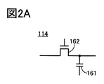
- FIG. 2A is a circuit diagram illustrating one embodiment of the present invention.
- FIG. 2B is a circuit diagram illustrating one embodiment of the present invention.
- FIG. 3A is a block diagram illustrating one embodiment of the present invention.
- FIG. 3B is a block diagram illustrating one embodiment of the present invention.
- FIG. 4 is a block diagram illustrating one embodiment of the present invention.
- FIG. 5A is a block diagram illustrating operation of the power storage device of one embodiment of the present invention.
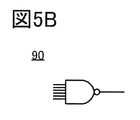
- FIG. 5B is a circuit diagram illustrating one embodiment of the present invention.
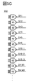
- FIG. 5C is a circuit diagram illustrating one embodiment of the present invention.
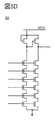
- FIG. 5D is a circuit diagram illustrating one embodiment of the present invention.
- FIG. 5A is a block diagram illustrating operation of the power storage device of one embodiment of the present invention.
- FIG. 5B is a circuit diagram illustrating one embodiment of the present invention.
- FIG. 6 is a block diagram illustrating one embodiment of the present invention.
- FIG. 7A is a circuit diagram illustrating one embodiment of the present invention.
- FIG. 7B is a circuit diagram illustrating one embodiment of the present invention.
- FIG. 8A is a circuit diagram illustrating one embodiment of the present invention.
- FIG. 8B is a circuit diagram illustrating one embodiment of the present invention.
- FIG. 8C is a circuit diagram illustrating one embodiment of the present invention.
- FIG. 9 is a circuit diagram illustrating one embodiment of the present invention.
- FIG. 10 is a sectional view showing a configuration example of a semiconductor device.
- FIG. 11 is a cross-sectional view showing a configuration example of a semiconductor device.
- FIG. 12A is a cross-sectional view showing a structural example of a transistor.
- FIG. 10 is a sectional view showing a configuration example of a semiconductor device.
- FIG. 11 is a cross-sectional view showing a configuration example of a semiconductor device.
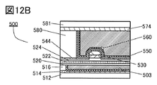
- FIG. 12B is a cross-sectional view showing a structural example of a transistor.
- FIG. 12C is a cross-sectional view showing a structural example of a transistor.
- FIG. 13A is a perspective view showing an example of a semiconductor device.
- FIG. 13B is a perspective view showing an example of a semiconductor device.
- FIG. 13C is a perspective view showing an example of a semiconductor device.
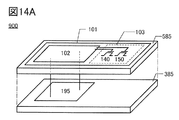
- FIG. 14A is a perspective view showing an example of a semiconductor device.
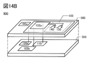
- FIG. 14B is a perspective view showing an example of a semiconductor device.
- FIG. 15A is a flowchart showing a manufacturing process of an electronic component.
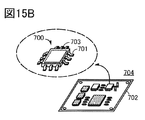
- FIG. 15B is a schematic perspective view showing a manufacturing process of the electronic component.
- FIG. 15A is a flowchart showing a manufacturing process of an electronic component.
- FIG. 15B is a schematic perspective view showing a manufacturing process of the electronic component.
- FIG. 15A is a flowchart showing a manufacturing process of an electronic
- FIG. 16A is a diagram illustrating an electric device of one embodiment of the present invention.
- FIG. 16B is a diagram illustrating an electric device of one embodiment of the present invention.
- FIG. 16C is a diagram illustrating an electric device of one embodiment of the present invention.
- FIG. 16D is a diagram illustrating an electric device of one embodiment of the present invention.
- FIG. 17A is a diagram illustrating an electric device of one embodiment of the present invention.
- FIG. 17B is a diagram illustrating an electric device of one embodiment of the present invention.
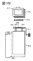
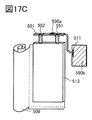
- FIG. 17C is a diagram illustrating an electric device of one embodiment of the present invention.
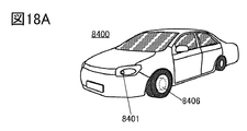
- FIG. 18A is a diagram illustrating an electric device of one embodiment of the present invention.
- FIG. 18B is a diagram illustrating an electric device of one embodiment of the present invention.
- FIG. 18A is a diagram illustrating an electric device of one embodiment of the present invention.
- FIG. 18B is a diagram illustrating an electric device of one embodiment of the present invention.
- FIG. 18C is a diagram illustrating an electric device of one embodiment of the present invention.
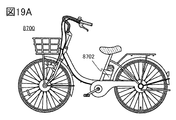
- FIG. 19A is a diagram illustrating an electric device of one embodiment of the present invention.
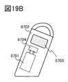
- FIG. 19B is a diagram illustrating an electric device of one embodiment of the present invention.
- FIG. 20A is a diagram illustrating an electric device of one embodiment of the present invention.
- FIG. 20B is a diagram illustrating an electric device of one embodiment of the present invention.
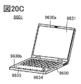
- FIG. 20C is a diagram illustrating an electric device of one embodiment of the present invention.
- 21A and 21B are diagrams illustrating electric devices of one embodiment of the present invention.
- 22A is a diagram illustrating an electric device of one embodiment of the present invention.
- FIG. 22B is a diagram illustrating an electric device of one embodiment of the present invention.
- FIG. 22C is a diagram illustrating an electric device of one embodiment of the present invention.
- FIG. 22D is a diagram illustrating an electric device of one embodiment of the present invention.
- FIG. 22E is a diagram illustrating an electric device of one embodiment of the present invention.
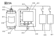
- 23A, 23B, and 23C are examples of a system of one embodiment of the present invention.
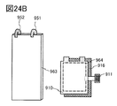
- 24A and 24B are examples of a system of one embodiment of the present invention.
- FIG. 25 is an example of a system of one embodiment of the present invention.
- FIG. 26 illustrates an operation example of the power storage device of one embodiment of the present invention.
- 27A, 27B, and 27C show the operation results of the comparator.
- FIG. 28 is a perspective view showing one embodiment of the present invention.
- FIG. 29 is a photograph showing one embodiment of the present invention.
- FIG. 30 is a cross-sectional view showing a structural example of a semiconductor.
- 31A is a cross-sectional view illustrating a structural example of a transistor.
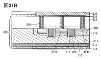
- 31B is a cross-sectional view illustrating a structural example of a transistor.
- FIG. 31C is a cross-sectional view illustrating a structural example of a transistor.
- the ordinal numbers “first”, “second”, and “third” are added to avoid confusion among constituent elements. Therefore, the number of components is not limited. Moreover, the order of the components is not limited. Further, for example, a constituent element referred to as “first” in one of the embodiments of the present specification and the like is a constituent element referred to as “second” in another embodiment or in the claims. There is a possibility. Further, for example, the component referred to as “first” in one of the embodiments of the present specification and the like may be omitted in another embodiment or the claims.
- the position, size, range, etc. of each configuration shown in the drawings, etc. may not represent the actual position, size, range, etc., in order to facilitate understanding of the invention. Therefore, the disclosed invention is not necessarily limited to the position, size, range, or the like disclosed in the drawings and the like.
- the resist mask or the like may be unintentionally reduced due to a process such as etching, but it may not be reflected in the drawing for easy understanding.
- top view also called “plan view”
- perspective view some of the components may be omitted to make the drawing easier to understand.
- electrode and “wiring” do not functionally limit these constituent elements.
- electrode may be used as part of “wiring” and vice versa.
- electrode and wiring include the case where a plurality of “electrodes” and “wirings” are integrally formed.
- electrode B on insulating layer A it is not necessary that the electrode B is directly formed on the insulating layer A, and another structure is provided between the insulating layer A and the electrode B. Do not exclude those that contain elements.
- the functions of the source and the drain are switched depending on operating conditions such as when transistors of different polarities are used or when the direction of the current changes in circuit operation. Therefore, which is the source or the drain is limited. Is difficult. Therefore, in this specification, the terms “source” and “drain” can be interchanged.
- “electrically connected” includes a case of being directly connected and a case of being connected via “thing having some electrical action”.
- the “object having some kind of electrical action” is not particularly limited as long as it can transfer an electric signal between the connection targets. Therefore, even in the case of being expressed as “electrically connected”, there is a case where the actual circuit does not have a physical connection portion and only the wiring extends.
- parallel means a state in which two straight lines are arranged at an angle of ⁇ 10° or more and 10° or less, for example. Therefore, a case of -5° or more and 5° or less is also included.
- vertical and orthogonal refer to, for example, a state in which two straight lines are arranged at an angle of 80° or more and 100° or less. Therefore, the case of 85° or more and 95° or less is also included.
- the resist mask is removed after the etching process is completed, unless otherwise specified.
- the voltage often indicates a potential difference between a certain potential and a reference potential (for example, ground potential or source potential). Therefore, the voltage and the potential can be paraphrased in many cases. In this specification and the like, voltage and potential can be paraphrased unless otherwise specified.
- the “semiconductor” can be replaced with the “insulator” and used.
- the boundary between the “semiconductor” and the “insulator” is ambiguous, and it is difficult to strictly distinguish the two. Therefore, the “semiconductor” and the “insulator” described in this specification may be interchangeable with each other.
- the “semiconductor” can be replaced with the “conductor” and used.
- the boundary between the “semiconductor” and the “conductor” is ambiguous, and it is difficult to strictly distinguish the two. Therefore, the “semiconductor” and the “conductor” described in this specification may be interchangeable with each other.
- the “on state” of a transistor refers to a state where the source and drain of the transistor can be regarded as being electrically short-circuited (also referred to as “conduction state”). Further, the “off state” of a transistor refers to a state in which the source and the drain of the transistor can be considered to be electrically disconnected (also referred to as a “non-conduction state”).
- the “on-state current” may mean a current flowing between the source and the drain when the transistor is on.
- the “off current” may refer to a current flowing between the source and the drain when the transistor is off.
- the high power supply potential VDD (hereinafter, also simply referred to as “VDD” or “H potential”) indicates a power supply potential higher than the low power supply potential VSS.
- the low power supply potential VSS (hereinafter, also simply referred to as “VSS” or “L potential”) indicates a power supply potential lower than the high power supply potential VDD.
- the ground potential can be used as VDD or VSS. For example, when VDD is the ground potential, VSS is lower than the ground potential, and when VSS is the ground potential, VDD is higher than the ground potential.
- gate means part or all of a gate electrode and a gate wiring.
- a gate wiring refers to a wiring for electrically connecting a gate electrode of at least one transistor to another electrode or another wiring.
- a source refers to part or all of a source region, a source electrode, and a source wiring.
- the source region refers to a region of the semiconductor layer whose resistivity is equal to or lower than a certain value.
- the source electrode refers to a conductive layer in a portion connected to the source region.
- a source wiring refers to a wiring for electrically connecting a source electrode of at least one transistor to another electrode or another wiring.
- drain means part or all of a drain region, a drain electrode, and a drain wiring.
- the drain region refers to a region of the semiconductor layer whose resistivity is equal to or lower than a certain value.
- the drain electrode refers to a conductive layer in a portion connected to the drain region.
- the drain wiring refers to a wiring for electrically connecting the drain electrode of at least one transistor to another electrode or another wiring.
- the battery control circuit of one embodiment of the present invention or a power storage device including the battery control circuit may be referred to as “BTOS”.
- BTOS may be able to construct a system with low power consumption.
- BTOS may be able to construct a system with a simple circuit.
- the battery control circuit of one embodiment of the present invention has a function of controlling a battery. For example, it has a function of changing the charging or discharging condition of the battery.
- the conditions include, for example, current density, upper limit voltage, lower limit voltage, mode switching, and the like. Examples of modes include a constant current mode and a constant voltage mode.
- the battery control circuit of one embodiment of the present invention preferably has a function of protecting the battery. For example, it has a function of stopping charging or discharging of a battery. For example, it has a function of discharging the battery when overcharge is detected. For example, it has a function of detecting an abnormality of the battery and stopping the operation of the battery or changing the condition of the battery.
- Stopping the operation of the battery may be, for example, stopping charging or stopping discharging.
- the battery abnormality includes, for example, overcharge, overdischarge, overcurrent during charging, overcurrent during discharging, short circuit, micro short circuit described later, and deviation of operating temperature from a predetermined range.
- the battery control circuit of one embodiment of the present invention may be called a battery protection circuit.
- FIG. 1 illustrates an example of the power storage device 100.
- the power storage device 100 shown in FIG. 1 includes a battery control circuit 101, a voltage generation circuit 119, and an assembled battery 120.
- the battery control circuit 101 is preferably mounted with a circuit including a transistor including an oxide semiconductor in a channel formation region (hereinafter referred to as an OS transistor).
- the battery control circuit 101 has a cell balance circuit 130, a detection circuit 185, a detection circuit 186, a detection circuit MSD, a detection circuit SD, a temperature sensor TS, a decoder 160, and a logic circuit 182.
- the battery control circuit 101 has a transistor 140 and a transistor 150.
- OS transistors can be used as the transistors 140 and 150.
- An OS transistor can be used as a transistor included in the cell balance circuit 130, the detection circuit 185, the detection circuit 186, the detection circuit MSD, the detection circuit SD, the temperature sensor TS, the decoder 160, and the logic circuit 182 included in the battery control circuit 101.
- These circuits may include an OS transistor and a Si transistor formed in a layer below the layer provided with the OS transistor. Alternatively, these circuits may be configured by OS transistors, and a circuit different from these circuits may be configured by using Si transistors in the lower layer. Alternatively, the Si transistor may not be provided in the lower layer of these circuits.
- the transistor included in the decoder 160 may be an OS transistor, and the transistor included in the voltage generation circuit 119 below the OS transistor may be an Si transistor.
- the battery control circuit 101 can be provided over the same substrate.
- a terminal AA, a terminal AB and a terminal AH which will be described later are used for exchanging signals with a circuit provided on a substrate different from the battery control circuit 101, for example, an arithmetic circuit such as MCU or MPU. ..
- Terminal AA, terminal AB and terminal AH are sometimes called “external terminals”.
- the assembled battery 120 has a plurality of battery cells 121.
- FIG. 1 shows an example having N battery cells 121.
- the kth battery cell (k is an integer of 1 or more and N or less) may be referred to as a battery cell 121(k).
- the plurality of battery cells included in the assembled battery 120 are electrically connected in series.
- the battery cell for example, a secondary battery described in the embodiment described later can be used.
- a secondary battery having a wound battery element can be used.
- the battery cell preferably has an outer package.
- a cylindrical exterior body, a rectangular exterior body, or the like can be used.
- a metal plate covered with an insulator, a metal film sandwiched between insulators, or the like can be used as the material of the outer package.
- the battery cell has, for example, a pair of positive electrode and negative electrode.
- the battery cell may have a terminal electrically connected to the positive electrode and a terminal electrically connected to the negative electrode.
- the battery cell may have a part of the structure of the battery control circuit of one embodiment of the present invention.
- the cell balance circuit 130 has a function of controlling charging of individual battery cells 121 included in the assembled battery 120.
- the detection circuit 185 has a function of detecting overcharge and overdischarge of the assembled battery 120.
- the detection circuit 186 has a function of detecting discharge overcurrent and charge overcurrent of the assembled battery 120.
- the detection circuit MSD has a function of detecting a micro short circuit.
- Micro short-circuit refers to a minute short circuit inside the secondary battery, and it is not such that the positive and negative electrodes of the secondary battery short-circuit and cannot be charged and discharged, but a minute short-circuited part. This is a phenomenon in which short-circuit current flows for a short period of time.
- the cause of the micro short circuit is that deterioration occurs due to multiple charging/discharging, metal elements such as lithium and cobalt are deposited inside the battery, and the deposit grows, causing a part of the positive electrode and one of the negative electrodes. It is presumed that a local concentration of electric current occurs at a part, a part of the separator does not function, or a side reaction product is generated.
- the detection circuit SD detects, for example, a short circuit in a circuit group operated by using the assembled battery 120. Further, the detection circuit SD detects, for example, the charging current and the discharging current of the assembled battery 120.
- the battery control circuit 101 is electrically connected to the terminals VC1 to VCN electrically connected to the positive electrodes of the N battery cells 121 included in the assembled battery 120 and the negative electrode of the Nth battery cell 121. And a terminal VSSS.
- the battery control circuit 101 also has a terminal group AA, a terminal group AB, and a terminal group AH.
- Each of the terminal group AA, the terminal group AB, and the terminal group AH has one terminal or a plurality of terminals.
- the decoder 160 includes a signal applied to the terminal SH6 included in the cell balance circuit 130, a signal applied to the terminals SH1 and SH2 included in the detection circuit 185, a signal applied to the terminals SH3 and SH4 included in the detection circuit 186, and a terminal included in the detection circuit SD. It has a function of generating and outputting a signal given to the SH5 and a signal given to the terminal SH8-1, the terminal SH8-2 and the terminal SH8-3 of the temperature sensor TS.
- the voltage generation circuit 119 has a digital-analog conversion circuit 190.
- the potential generated in the voltage generation circuit 119 is supplied to the terminal group AB after being converted into an analog signal by the digital-analog conversion circuit 190, for example.
- the battery control circuit of one embodiment of the present invention uses a number corresponding to the number of required potentials.
- the respective potentials can be supplied without providing the terminals. Therefore, the number of terminals can be reduced.
- circuits such as the cell balance circuit 130 and the detection circuit 185 each include an OS transistor, whereby the number of terminals in the terminal group AB can be reduced. ..
- a signal input from one terminal can be sequentially supplied to each circuit and held by a memory element including an OS transistor. In the example shown in FIG.
- terminal VT one terminal is electrically connected to the terminal group AB, and the terminal VT is the cell balance circuit 130, the detection circuit 185, the detection circuit 186, the detection circuit SD, and the temperature sensor. An analog signal is given to each TS.
- the power supply of the voltage generation circuit 119 is turned off or the voltage generation circuit 119 is put into a standby state after the signals are supplied to the respective circuits. As a result, the power consumption of the voltage generation circuit 119 can be reduced. For example, power gating of the voltage generation circuit may be performed.
- the configuration of the storage element 114 shown in FIG. 2A can be used as the storage element.
- the memory element 114 illustrated in FIG. 2A includes a capacitor 161 and a transistor 162.
- an OS transistor As the transistor 162.
- the memory element 114 including an OS transistor leakage current flowing between the source and the drain at the time of off (hereinafter referred to as off current) is extremely low, which is desirable. Can be held in the memory element.
- FIG. 2B is different from FIG. 2A in that the transistor 162 included in the memory element 114 has a second gate.
- the second gate may be called a back gate or a bottom gate.
- the second gate included in the OS transistor will be described in detail in later embodiments.
- the terminal group AH preferably has a function of giving a signal to the logic circuit 182 and a function of giving a signal from the logic circuit 182 to a circuit provided outside the battery control circuit 101.
- the logic circuit 182 has a function of controlling the transistors 140 and 150 according to output signals from the detection circuit 185, the detection circuit 186, the detection circuit SD, the detection circuit MSD, and the temperature sensor TS. Further, the logic circuit 182 may supply a signal to a charging circuit provided outside or inside the battery control circuit 101. In this case, for example, charging of the secondary battery is controlled according to the signal given from the logic circuit 182 to the charging circuit.
- the charging circuit has a function of controlling the charging condition of the battery, for example.
- a signal for controlling the condition for charging the battery is controlled by another circuit, for example, the decoder 160, the cell balance circuit, the overcharge detection circuit, the transistor 140, the transistor 150, the transistor 140, and the transistor 150 included in one embodiment of the present invention. Circuit, etc.
- the transistors 140 and 150 have a function of controlling charging or discharging of the assembled battery 120.
- the transistor 140 is controlled to be in a conductive state or a non-conductive state by a control signal T1 provided by the logic circuit 182, and whether or not to charge the assembled battery 120 is controlled.
- the transistor 150 is controlled to be conductive or non-conductive by a control signal T2 provided by the logic circuit 182, and whether or not to discharge the assembled battery 120 is controlled.
- one of a source and a drain of the transistor 140 is electrically connected to the terminal VSSS.
- the other of the source and the drain of the transistor 140 is electrically connected to one of the source and the drain of the transistor 150.
- the other of the source and the drain of the transistor 150 is electrically connected to the terminal VM.
- the terminal VM is electrically connected to the negative pole of the charger, for example. Further, the terminal VM is electrically connected to, for example, a load at the time of discharging.
- the battery control circuit 101 may have a function of observing a voltage value (monitor voltage) of each terminal of the battery cell 121 included in the battery pack 120 and a current value (monitor current) flowing through the battery pack.
- a voltage value (monitor voltage) of each terminal of the battery cell 121 included in the battery pack 120
- a current value (monitor current) flowing through the battery pack.
- the on-current of the transistor 140 or the transistor 150 may be observed as a monitor current.
- a resistance element may be provided in series with the transistor 140 or the like and the current value of the resistance element may be observed.
- the battery control circuit 101 may also have a function of measuring the temperature of the battery cell 121 and controlling charging and discharging of the battery cell based on the measured temperature. For example, since the resistance of the secondary battery may increase at low temperatures, the charging current density and the discharging current density may be reduced. Moreover, since the resistance of the secondary battery may decrease at a high temperature, the discharge current density may be increased. In addition, when the charging current is increased at a high temperature and there is a concern that the characteristics of the secondary battery are deteriorated, the charging current may be controlled to suppress the deterioration, for example. Data such as charge conditions and discharge conditions are preferably stored in a memory circuit or the like included in the battery control circuit 101 of one embodiment of the present invention. Further, the temperature of the battery control circuit 101 or the assembled battery 120 may rise due to charging. In such a case, it is preferable to control charging according to the measured temperature. For example, the charging current may be suppressed as the temperature rises.
- the cell balance circuit 130 and the detection circuit 185 of one embodiment of the present invention are preferably provided one for each of the plurality of battery cells 121 included in the assembled battery 120.
- FIG. 3A shows the cell balance circuit 130 and the detection circuit 185 corresponding to one battery cell 121.
- FIG. 3A shows an example in which the cell balance circuit 130 and the detection circuit 185 are connected to one battery cell 121.
- the detection circuit 185 includes a circuit 185c and a circuit 185d.
- the detection circuit 185 has a function of detecting overcharge, and the detection circuit 186 has a function of detecting overdischarge.
- the transistor 132 and the resistance element 131 are connected in series, one of the source and the drain of the transistor 132 is electrically connected to the negative electrode of the battery cell 121, and the other is electrically connected to one electrode of the resistance element.
- the other electrode of the resistance element is electrically connected to the positive electrode of the secondary battery.
- one of a source and a drain of the transistor 132 is electrically connected to a positive electrode of the battery cell 121, the other is electrically connected to one electrode of the resistance element 131, and the other electrode of the resistance element 131 is electrically connected to a negative electrode of the battery cell 121. May be done.
- the cell balance circuit 130 and the detection circuit 185 each have a switch SW.
- Each switch SW is electrically connected to the terminal VC2 and a terminal to which a ground potential is applied, and has a function of applying the potential of either terminal to one electrode of the capacitor 161.
- the cell balance circuit 130 and the detection circuit 185 may have a common switch SW.
- the cell balance circuit 130, the circuit 185c, and the circuit 185d each include a comparator 113 and a storage element 114.
- the memory element 114 has a capacitor 161 and a transistor 162.
- a common terminal, here, a terminal VT is electrically connected to one of a source and a drain of each transistor 162 included in the cell balance circuit 130, the circuit 185c, and the circuit 185d.
- the other electrode of the source and the drain of each transistor 162 is electrically connected to the other electrode of the capacitor 161 included in each circuit and either the non-inverting input terminal or the inverting input terminal of the comparator 113. ..
- the cell balance circuit 130 is electrically connected to the positive electrode and the negative electrode of the battery cell 121.
- the positive electrode of the battery cell 121 is electrically connected to the terminal VC1, and the negative electrode is electrically connected to the terminal VC2.
- the inverting input terminal of the comparator 113 is electrically connected to the other of the source and the drain of the transistor 162, and the terminal SH6 is electrically connected to the gate of the transistor 162.
- the non-inverting input terminal of the comparator 113 is preferably electrically connected to the terminal VC1. Alternatively, as shown in FIG.
- the non-inverting input terminal of the comparator 113 may be supplied with a voltage obtained by dividing the resistance between the terminals VC1 and VC2.
- a node connected to the other of the source and the drain of the transistor 162 is a node N6.
- the detection circuit 185 is electrically connected to the positive electrode and the negative electrode of the battery cell 121.
- the inverting input terminal of the comparator is electrically connected to the other of the source and the drain of the transistor 162, and the terminal SH1 is electrically connected to the gate of the transistor 162.
- the non-inverting input terminal of the comparator 113 is preferably electrically connected to the terminal VC1.
- the non-inverting input terminal of the comparator 113 may be supplied with a voltage obtained by dividing the resistance between the terminals VC1 and VC2.
- a node connected to the other of the source and the drain of the transistor 162 is a node N1.
- the non-inverting input terminal of the comparator is electrically connected to the other of the source and the drain of the transistor 162, and the terminal SH2 is electrically connected to the gate of the transistor 162.
- the inverting input terminal of the comparator 113 is preferably electrically connected to the terminal VC1.
- the inverting input terminal of the comparator 113 may be supplied with a voltage obtained by resistance-dividing the terminals VC1 and VC2.
- a node connected to the other of the source and the drain of the transistor 162 is a node N2.
- the transistor 162 is turned off at a node (here, the node N6, the node N1, and the node N2) to which the other electrode of the capacitor 161 included in each circuit is connected. The electric potential is held.
- the terminal VT sequentially supplies analog signals to the cell balance circuit 130, the circuit 185c, and the circuit 185d.
- An analog signal is sequentially applied to and held at nodes N6, N1 and N2.
- the transistor 162 connected to the node is turned off, whereby the potential of the first node is held.
- the potential of the second node is supplied and held, and then the potential of the third node is supplied and held.
- the on/off control of the transistor 162 is controlled by a signal output from the decoder 160 (here, a signal applied to the terminal SH1, the terminal SH2, and the terminal SH6).
- the potential applied to one electrode of the capacitor 161 is changed from the ground potential to the potential of the terminal VC2 by switching the switch SW, and the node N6, the node N1, and Each potential held in the node N2 can be changed by the difference between the terminal VC2 and the ground potential.
- the cell balance circuit 130 and the detection circuit 185 can hold the sum of the potentials given from the terminal VT and the potential of the terminal VC2 at the node N6, the node N1 and the node N2.
- the terminal VC2 is the negative potential of the battery cell 121
- the node N6, the node N1, and the node N2 must hold the sum of the potential given from the terminal VT and the negative potential of the battery cell 121.
- FIG. 4 shows an example in which the cell balance circuit 130 and the detection circuit 185 shown in FIG. 3A are provided for each of the battery cells 121 included in the assembled battery 120.
- the assembled battery 120 has N battery cells 121.
- the kth battery cell 121 (k is an integer of 1 or more and N or less) is referred to as a battery cell 121(k).
- the cell balance circuit 130 connected to the battery cell 121(k) is referred to as a cell balance circuit 130(k)
- the detection circuit 185 connected to the battery cell 121(k) is referred to as a detection circuit 185(k).
- the cell balance circuits 130(1) to 130(N) are referred to as a cell balance circuit 130.
- the detection circuits 185(1) to 185(N) are referred to as a detection circuit 185.
- the cell balance circuit 130 and the detection circuit 185 have a function of individually controlling the voltage difference (difference between the positive electrode and the negative electrode) between both ends of each of the plurality of connected battery cells 121.
- the cell balance circuit 130 can cause the storage element 114 to hold a preferable value as the first upper limit voltage of the positive electrode for each battery cell 121.
- the node N6 included in the cell balance circuit 130(k) is referred to as a node N6(k).
- the negative electrode potential of the battery cell (k) is electrically connected to the switch SW included in the cell balance circuit 130(k). That is, the switch SW included in each cell balance circuit 130 is supplied with a potential corresponding to the negative electrode of each battery cell.
- the node N6(k) can hold the sum of the potential given from the terminal VT and the potential of the negative electrode of the battery cell 121(k).
- each cell balance circuit can be given a potential using the common potential given from the terminal VT with the negative electrode of each battery cell as a reference, and therefore the terminals can be provided to N battery cells. Can be common. Therefore, the number of terminals can be reduced.
- the cell balance circuit 130 controls whether the transistor 132 is turned on or off depending on the relationship between the voltage of the positive electrode of the battery cell 121 and the voltage of the non-inverting input terminal of the comparator 113. I do. By controlling the transistor 132, the ratio of the amount of current flowing through the resistance element 131 and the amount of current flowing through the battery cell 121 can be adjusted. For example, when the charging of the battery cell 121 is stopped, a current is passed through the resistance element 131 to limit the current flowing through the battery cell 121.
- a plurality of battery cells 121 are electrically connected in series between a terminal VDDD and a terminal VSSS. A plurality of battery cells 121 are charged by passing a current between the terminal VDDD and the terminal VSSS.
- the positive electrode of one of the plurality of battery cells 121 reaches a predetermined voltage and the current is limited.
- the current path between the terminal VDDD and the terminal VSSS is not interrupted, and the positive electrode is It is possible to continue charging the other battery cells 121 that have not reached the predetermined voltage. That is, in the battery cell 121 that has been charged, charging is stopped by turning on the transistor 132, and in the battery cell 121 that has not been charged, the transistor 132 is turned off and charging is continued.
- charging of one battery cell 121 having a low resistance may be completed first, and charging of a battery cell 121 having a higher resistance than that of a certain battery cell 121 may be insufficient. is there.
- insufficient charging means, for example, that the voltage difference between the positive electrode and the negative electrode is lower than a desired voltage.
- the voltage of the positive electrode of the battery cell 121 during charging can be controlled with reference to the voltage of the negative electrode of each battery cell.
- the cell balance circuit of one embodiment of the present invention without using a circuit provided outside the battery control circuit 101, for example, an arithmetic circuit such as an MPU or an MCU, the charging voltage of one battery cell or a plurality of battery cells, or The charge capacity, etc. can be controlled.
- an arithmetic circuit such as an MPU or an MCU
- the charging voltage of one battery cell or a plurality of battery cells, or The charge capacity, etc. can be controlled.
- the N cell balance circuits 130 it is possible to reduce variations in the state of the plurality of battery cells 121 after charging, for example, when fully charged. Therefore, the capacity of the assembled battery 120 as a whole may increase. In addition, increasing the capacity may reduce the number of charge/discharge cycles of the battery cells 121, and thus the durability of the assembled battery 120 may increase.
- the circuit 185c can cause the storage element 114 to hold the second upper limit voltage of the positive electrode in charging the battery cell 121 for each battery cell 121.
- the second upper limit voltage may be called an overcharge voltage.
- the circuit 185d can cause the storage element 114 to hold the lower limit voltage of the positive electrode in discharging.
- the lower limit voltage may be called an overdischarge voltage.
- the comparator constituting the detection circuit 185 may be a hysteresis comparator having different thresholds when the output changes from the L level to the H level and when the output changes from the H level to the L level. It is preferable that the storage element connected to the reference potential input portion of the hysteresis comparator has a function of holding two threshold values.
- the node N1 and the node N2 included in the detection circuit 185(k) are referred to as a node N1(k) and a node N2(k), respectively.
- the negative electrode potential of the battery cell (k) is electrically connected to the switch SW included in the detection circuit 185(k). That is, the switch SW included in each detection circuit 185 is supplied with a potential corresponding to the negative electrode of each battery cell.
- the node N1(k) can hold the sum of the potential given from the terminal VT and the potential of the negative electrode of the battery cell 121(k).
- the node N2(k) can hold the sum of the potential given from the terminal VT and the potential of the negative electrode of the battery cell 121(k).
- each detection circuit can be supplied with a potential using the common potential given from the terminal VT with the negative electrode of each battery cell as a reference, the terminals are shared by N battery cells. Can be Therefore, the number of terminals can be reduced.
- the detection circuit 185 detects overcharge and overdischarge of one battery cell or a plurality of battery cells without using a circuit provided outside the battery control circuit 101, for example, an arithmetic circuit such as MPU or MCU, Cell protection can be performed.
- a voltage drop due to overdischarge is detected, the control circuit of one embodiment of the present invention interrupts the discharge current and prevents the voltage drop. If the cutoff of the discharge current is insufficient, a leak current may occur and the voltage may drop.
- a circuit configuration using power gating may suppress the leak current. In addition, the leak current may be suppressed by the circuit configuration using the OS transistor.
- the upper limit voltage of each battery cell is controlled by the cell balance circuit connected to the battery cell and the circuit that detects overcharge.
- the upper limit voltage detected by the cell balance circuit is lower than the upper limit voltage detected by the circuit for detecting overcharge, for example. Therefore, in the process of charging, the cell balance circuit detects the reaching of the upper limit voltage of the battery cell in the first step and changes the charging condition. Here, for example, the charging current density is lowered. Alternatively, the discharge may be started. After that, when the reaching of the upper limit voltage detected by the circuit for detecting overcharge is detected as the charging voltage of the battery cell increases, the charging condition of the battery cell is changed in the second step. Here, for example, charging is stopped and discharging is started.
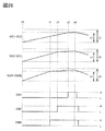
- the cell balance circuit 130 includes a voltage VC1 ⁇ VC2 and a voltage VC2 that are the potential differences between the positive and negative electrodes of the battery cell 121(1), the battery cell 121(2), and the battery cell 121(n).
- a high potential signal is output from terminals CB1, CB2 and CBN which are output terminals of the comparator corresponding to each battery cell.
- the assembled battery 120 is charged during the period from time t0 to time t1.
- the voltage VCN-VSSS exceeds the voltage v1
- a high potential signal is output from the terminal CBN, and the high potential signal is applied to the gate of the transistor 132 connected in parallel to the battery cell 121(n), A current flows through the transistor 132, and the current flowing through the battery cell 121(n) becomes small or hardly flows.
- the voltage (VC2-VC3) exceeds the voltage v1 and a high-potential signal is output from the terminal CB2, and the current flowing through the battery cell 121(2) becomes small or hardly flows.
- the voltage (VC1-VC2) exceeds the voltage v1 and a high-potential signal is output from the terminal CB1, and the current flowing through the battery cell 121(1) becomes small or hardly flows.
- the battery pack 120 starts to be discharged, and the voltage (VC1-VC2), the voltage (VC2-VC3), and the voltage (VCN-VSSS) decrease.
- the voltage (VC1-VC2), the voltage (VC2-VC3) and the voltage (VCN-VSSS) become smaller than the voltage v1, low potential signals are output from the terminals CB1, CB2 and CBN.
- the circuit 185c is overloaded.
- a high potential signal is applied to the gate of the transistor 140, for example, and the charging is stopped.
- the value input to the comparator 113 may be a value obtained by dividing the voltage difference between the positive electrode and the negative electrode of the battery cell by resistance division.
- values obtained by dividing the voltage v1 and the voltage v2 by resistance division may be used.
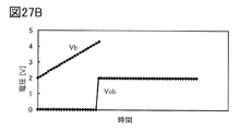
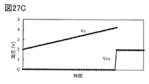
- a comparator 113 in which a memory element 114 using an OS transistor was connected to an inverting input terminal was prepared and its operation was confirmed.
- the voltage under three different conditions was sequentially applied to the non-inverting input terminal and the inverting input terminal of the comparator 113 to confirm the operation.
- the voltage at the non-inverting input terminal is voltage Va and the voltage obtained at the output terminal is Voa.
- the voltage at the non-inverting input terminal is Vb, and the voltage obtained at the output terminal is Vob.
- the voltage at the non-inverting input terminal is Vc and the voltage obtained at the output terminal is Voc.
- the voltage Va a value obtained by dividing the voltage (VC1-VC2) by 1/4 by resistance division, as the voltage Vb by dividing the voltage (VC1-VC2) by 1/4 by resistance division, and as the voltage Vc (voltage VCN-VSSS) are shown. Values were assumed to be 1/4 by resistance division and input.
- the inverting input terminal was given a voltage in which 4.2V was made 1/4 under the first condition, the second condition, and the third condition, and the value was held by the memory element 114.
- 4.2V is assumed to be, for example, a value obtained by adding 2.2V as a predetermined potential difference detected by the cell balance circuit to the negative electrode potential 2V. That is, the voltage v1 shown in FIG. 26 is assumed to be 4.2V.
- FIG. 27A the input voltage Va and the output voltage Voa are input as the result when the first condition is given to the comparator, and in FIG. 27B, the second voltage is input as the result when the second condition is given to the comparator.
- the voltage Vb and the output voltage Vob are shown in FIG. 27C, and the input voltage Vc and the output voltage Voc are shown as a result when the third condition is applied to the comparator, respectively. It was confirmed that when the input voltage exceeds the value stored in the inverting input terminal, a high potential signal is output from each comparator.
- FIG. 5A shows an example in which a 6-bit signal is given from the terminal AA to the decoder 160.
- FIG. 5A shows only an example, and the number of bits of the signal supplied from the terminal AA to the decoder 160 is not limited.
- FIG. 5B shows a circuit symbol of the NAND circuit 90.
- the decoder 160 can be configured using a plurality of NAND circuits 90.
- FIG. 5D shows a specific example of the NAND circuit 90.
- a high-potential power supply potential is applied to the wiring VDD.
- FIG. 6 shows an example of the logic circuit 182.
- the logic circuit 182 illustrated in FIG. 6 includes an interface circuit IF, a counter circuit CND, a latch circuit LTC, and a transistor 172.
- An OS transistor is preferably used as the transistor 172.
- the interface circuit IF is supplied with signals from the output terminals OUT11 and OUT12 of the detection circuit 185, signals from the output terminals OUT31 and OUT32 of the detection circuit 186, and signals from the output terminal OUT41 of the detection circuit SD. ..
- the output terminal OUT11 provides, for example, a signal corresponding to overcharge.
- the output terminal OUT12 gives a signal corresponding to over-discharge, for example.
- the output terminal OUT31 gives, for example, a signal corresponding to an overcurrent at the time of charging.
- the output terminal OUT32 gives, for example, a signal corresponding to an overcurrent at the time of discharging.
- the interface circuit IF gives the signal PG to the gate of the transistor 172 when detecting a signal for detecting an abnormality, for example, a signal corresponding to at least one of overcharge, overdischarge, and overcurrent.
- the transistor 172 is connected to the counter circuit.
- the counter circuit operates a counter and a delay circuit when the signal PG outputs a signal for turning on the transistor 172, more specifically, for example, a high potential signal.
- the operation of the counter circuit CND can be stopped or the counter circuit CND can be placed in a standby state. ..
- a signal res is applied from the interface circuit IF to the counter circuit CND and the latch circuit LTC.
- the signal res is a reset signal.
- the signal res is applied to the counter circuit CND to start counting.
- the signal en is an enable signal.
- the counter circuit CND starts or stops its operation according to the signal en.
- the counter circuit CND When a signal for detecting an abnormality is given to the interface circuit IF, the counter circuit CND counts for a certain period, and then a signal corresponding to the detected abnormality is given to the latch circuit LTC via the counter circuit CND. ..
- the latch circuit LTC gives a signal for turning off the transistor to the gate of the transistor 140 or the transistor 150 according to the detected abnormality.
- FIG. 7A shows an example of a circuit diagram of the detection circuit 186.
- the detection circuit 186 has two comparators 113.
- a storage element 114 that holds a voltage corresponding to discharge overcurrent detection is electrically connected to the non-inverting input terminal of one comparator 113.
- the terminal SH3 is electrically connected to the gate of the transistor included in the memory element 114. Further, the terminal SENS is electrically connected to the inverting input terminal. When an overcurrent is detected by the voltage applied to the inverting input terminal, the output from the output terminal OUT32 is inverted.
- the terminal SENS is electrically connected to the non-inverting input terminal of the other comparator 113. Further, the storage element 114 corresponding to the detection of charging overcurrent is electrically connected to the inverting input terminal.
- the terminal SH4 is electrically connected to the gate of the transistor included in the memory element 114. When an overcurrent is detected by the voltage applied to the non-inverting input terminal, the output from the output terminal OUT31 is inverted.
- the temperature sensor TS has a function of measuring the temperature of the battery pack 120 or the power storage device 100 including the battery pack 120.
- FIG. 7B is a circuit diagram showing an example of the temperature sensor TS. The circuit diagram shown in FIG. 7B may represent a part of the circuit of the temperature sensor TS.
- Each applied voltage VT is held by the storage element 114 electrically connected to the inverting input terminal.
- the voltages Tm1, Tm2, and Tm3 may be supplied from the voltage generation circuit 119, for example.
- a voltage corresponding to the measured temperature is applied to the input terminal Vt.
- the input terminal Vt is given to each non-inverting input terminal of the three comparators 113.
- a signal is output from the output terminal (output terminal OUT51, output terminal OUT52, output terminal OUT53) of each comparator corresponding to the comparison result of the voltage applied to the input terminal Vt and the voltage of the inverting input terminal of each comparator 113. And the temperature can be determined.
- the OS transistor has the property that its resistance value decreases as the temperature rises. By utilizing this property, the ambient temperature can be converted into a voltage. This voltage may be applied to the input terminal Vt, for example.
- the logic circuit 182 detects the output of the temperature sensor TS, and when the temperature range in which the assembled battery 120 can operate is exceeded, the transistor 140 and/or the transistor 150 are made non-conductive, and charging and/or discharging are stopped. It may be configured.
- a lithium ion secondary battery cell can be used as the battery cell 121. Further, the battery cell 121 is not limited to the lithium ion secondary battery cell, and a material containing the element A, the element X, and oxygen can be used as the positive electrode material of the secondary battery.
- the element A is one or more selected from a group 1 element and a group 2 element.
- the Group 1 element for example, an alkali metal such as lithium, sodium or potassium can be used.
- the Group 2 element for example, calcium, beryllium, magnesium, or the like can be used.
- the element X for example, one or more selected from a metal element, silicon and phosphorus can be used.
- the element X is one or more selected from cobalt, nickel, manganese, iron, and vanadium. Typically, lithium cobalt composite oxide LiCoO 2 and lithium iron phosphate LiFePO 4 can be mentioned.
- a memory element including an OS transistor is used, so that the leakage current (hereinafter, off current) flowing between the source and the drain at the time of off is extremely low, and thus the reference voltage is used. Can be held in the storage element. At this time, since the power of the memory element can be turned off, the reference voltage can be held with extremely low power consumption by using the memory element having an OS transistor.
- a memory element having an OS transistor can hold an analog potential.
- the voltage of the secondary battery can be held in the memory element without being converted into a digital value by using the analog-digital conversion circuit.
- the conversion circuit becomes unnecessary and the circuit area can be reduced.
- the reference voltage can be rewritten and read by charging or discharging electric charge, so that it is possible to obtain and read the monitor voltage virtually unlimitedly.
- a memory element using an OS transistor is excellent in rewriting resistance because it does not involve structural change at the atomic level unlike a magnetic memory or a resistance change memory.
- instability due to an increase in electron trap centers is not recognized even in repeated rewriting operation unlike a flash memory.
- the OS transistor has extremely low off current and has good switching characteristics even in a high temperature environment. Therefore, even in a high temperature environment, charging or discharging of the battery pack 120 can be controlled without malfunction.
- the memory element using the OS transistor can be freely arranged by stacking it on a circuit using the Si transistor, so that the integration can be easily performed.
- the OS transistor can be manufactured at low cost because it can be manufactured using a manufacturing apparatus similar to that of the Si transistor.
- the OS transistor can be a four-terminal semiconductor element including a back gate electrode in addition to the gate electrode, the source electrode and the drain electrode.
- the input/output of the signal flowing between the source and the drain can be independently controlled according to the voltage applied to the gate electrode or the back gate electrode. Therefore, it is possible to design a circuit with the same idea as an LSI.
- the OS transistor has better electrical characteristics than the Si transistor in a high temperature environment. Specifically, since the ratio of the on-current to the off-current is large even at a high temperature of 100° C. or higher and 200° C. or lower, preferably 125° C. or higher and 150° C. or lower, good switching operation can be performed.
- an OS transistor may be used as the transistor 162.
- an OS transistor may be used as the transistor 132.
- OS transistors may be used as the transistors 140 and 150.
- the comparator may be configured using an OS transistor.
- a semiconductor device is configured such that, in a secondary battery which is being charged and discharged, a potential between a positive electrode and a negative electrode of the secondary battery is sampled (acquired) every predetermined time, and the sampled potential and the positive electrode after sampling are sampled. By comparing with the potential between the negative electrodes, it has a function of detecting a momentary potential fluctuation (here, the potential drops) due to a micro short circuit. By repeating the sampling every predetermined time, it is possible to cope with the potential fluctuation of the secondary battery during charging and discharging, and the semiconductor device can be operated by using the potential between the positive electrode and the negative electrode of the secondary battery.
- FIG. 8A is a circuit diagram showing a configuration example of the detection circuit MSD.
- the detection circuit MSD includes transistors 11 to 15, a capacitor C11, and a comparator 50. Note that in the drawings described in this specification and the like, main signal flows are indicated by arrows or lines, and power supply lines and the like may be omitted. A hysteresis comparator may be used as the comparator 50 included in the detection circuit MSD.
- the detection circuit MSD may perform detection in a plurality of battery cells connected in series, or may perform detection in each battery cell.
- FIG. 7 shows an example in which the detection circuit MSD is connected to the terminals VC1 and VSSS in the case of detecting the plurality of battery cells connected in series shown in FIG. 4, but the connection to the terminal VC1 and the terminals are shown. The connection to VSSS may be changed to the positive electrode and the negative electrode of one battery cell, respectively.
- the detection circuit MSD illustrated in FIG. 8A includes a terminal VC1, a wiring VB1_IN to which a predetermined potential VB1 is supplied, a wiring VB2_IN to which a predetermined potential VB2 is supplied, a wiring SH_IN to which a sampling signal is supplied, and an output terminal S_OUT.
- the predetermined potential VB1 is higher than the predetermined potential VB2, and the predetermined potential VB2 is higher than the potential of the terminal VSSS.
- FIG. 8B is different from FIG. 8A in that the transistors 11 to 15 included in the detection circuit MSD have the second gate.
- FIG. 8C is different from FIG. 8B in that it has a terminal VSSS, a storage element 114 connected to the wiring VB1_IN, and a storage element 114 connected to the wiring VB2_IN.
- FIG. 8C one of a source and a drain of the transistor 11, one of a source and a drain of the transistor 13, and one electrode of the capacitor C11 are electrically connected to the terminal VSSS. Since the potential VB1 and the potential VB2 are supplied to the wiring VB1_IN and the wiring VB2_IN through the memory element 114, respectively, the potential supplied by the memory element 114 can be held. Therefore, the power supply of the voltage generation circuit that supplies the potential VB1 and the potential VB2, more specifically, for example, the voltage generation circuit 119 can be turned off or can be in a standby state.
- the transistors 11 to 15 are n-channel type transistors. Although an example in which the detection circuit MSD is formed using an n-channel transistor is described in this specification and the like, a p-channel transistor may be used. Since a person skilled in the art can easily understand that a transistor is changed to a p-channel type from a circuit diagram configured by using an n-channel type transistor, description thereof will be omitted.
- one of the source and the drain of the transistor 11 is electrically connected to the terminal VSSS, and the other of the source and the drain of the transistor 11 is one of the source and the drain of the transistor 12 and the source of the transistor 15 or
- the transistor 11 is electrically connected to one of the drains, the gate of the transistor 11 is electrically connected to the wiring VB1_IN, and the other of the source and the drain of the transistor 12 and the gate of the transistor 12 are electrically connected to the terminal VC1.
- One of the source and the drain of the transistor 13 is electrically connected to the terminal VSSS, and the other of the source and the drain of the transistor 13 is the other of the source and the drain of the transistor 14 and the inverting input terminal of the comparator 50 (in FIG. 8A, , "-"), the gate of the transistor 13 is electrically connected to the wiring VB2_IN, and the other of the source and the drain of the transistor 14 and the gate of the transistor 14 are electrically connected to the terminal VC1. Connected to each other.
- the other of the source and the drain of the transistor 15 is electrically connected to the other terminal of the capacitor C11 and the non-inverting input terminal of the comparator 50 (denoted as “+” in FIG. 8A), and The gate is electrically connected to the wiring SH_IN, one terminal of the capacitor C11 is electrically connected to the terminal VSSS, and the output terminal of the comparator 50 is electrically connected to the output terminal S_OUT.
- one terminal of the capacitor C11 may be electrically connected to a wiring other than the terminal VSSS as long as the wiring is supplied with a predetermined potential.
- a connection portion where the other of the source and the drain of the transistor 11, the one of the source and the drain of the transistor 12, and the one of the source and the drain of the transistor 15 are electrically connected is referred to as a node N11.
- the other of the source and the drain of 13, the one of the source and the drain of the transistor 14, and the inverting input terminal of the comparator 50 are electrically connected to each other, which is referred to as a node N12.
- a connection portion where the other terminal, the other terminal of the capacitive element C11, and the non-inverting input terminal of the comparator 50 are electrically connected is referred to as a node N13.
- the transistors 11 and 12 form a first source follower
- the transistors 13 and 14 form a second source follower. That is, the gate of the transistor 11 corresponds to the input of the first source follower, and the first source follower outputs the signal to the node N11.
- the gate of the transistor 13 corresponds to the input of the second source follower, and the second source follower outputs a signal to the node N12.
- the sampling signal given to the wiring SH_IN becomes high level every predetermined time.
- a potential higher than the potential VB2 is applied as the potential VB1.
- the potential of the node N11 and the potential of the node N12 rise.
- the voltage of the secondary battery is converted into digital data by an analog-digital conversion circuit, and calculation is performed based on the digital data using a processor unit, etc.
- the waveform may be analyzed to detect a micro short or predict a micro short.
- the displacement of the voltage error at each time step is used to detect or predict the micro short circuit.
- the displacement of the voltage error is obtained by calculating the voltage error and calculating the difference from the previous step.
- a neural network may be used to improve the detection accuracy of micro shorts.
- a neural network is a method, and is a neural network process performed by a neural network unit (including, for example, a CPU (Central Processor Unit), a GPU (Graphics Processing Unit), an APU (Accelerated Processing Unit), and a memory). It should be noted that the APU refers to a chip that integrates a CPU and a GPU.
- a neural network unit including, for example, a CPU (Central Processor Unit), a GPU (Graphics Processing Unit), an APU (Accelerated Processing Unit), and a memory.
- the APU refers to a chip that integrates a CPU and a GPU.
- the secondary battery mounted in the device is random because discharge tends to depend on the user's usage, but charging is more predictable than discharge because charging conditions are fixed. By using a large number of charging curves as learning data, it is possible to predict an accurate value using a neural network. If the charge curve is acquired, the initial SOC(0), FCC, R 0 , R d , and C d can be obtained by using the neural network. A microprocessor or the like may be used for the calculation of the neural network.
- various acquired data are evaluated and learned using machine learning or artificial intelligence, the expected degree of deterioration of the secondary battery is analyzed, and if abnormal, charging of the secondary battery is stopped. , Or adjust the current density for constant current charging.
- a neural network is used to predict the deterioration state of the secondary battery.
- the neural network can be configured by a neural network having a plurality of hidden layers, that is, a deep neural network.
- the learning in the deep neural network may be referred to as deep learning.
- feature values are extracted from the learning data.
- a relative change amount that changes with time is extracted as a feature value, and a neural network is trained based on the extracted feature value.
- the learning means can learn the neural network based on different learning patterns for each time section.
- the connection weight applied to the neural network can be updated according to the learning result based on the learning data.
- Kalman filter is a kind of infinite impulse response filter. Further, the multiple regression analysis is one of the multivariate analysis, and the independent variable of the regression analysis is made plural. As the multiple regression analysis, there is a least squares method. While many time series of observation values are required in regression analysis, the Kalman filter has an advantage that an optimum correction coefficient can be sequentially obtained if a certain amount of data is accumulated. The Kalman filter can also be applied to non-stationary time series.
- a nonlinear Kalman filter (specifically, an unscented Kalman filter (also referred to as UKF)) can be used as a method of estimating the internal resistance and the state of charge (SOC) of the secondary battery. Further, an extended Kalman filter (also called EKF) can be used. SOC indicates a state of charge (also called a charge rate), and is an index that sets 100% when fully charged and 0% when completely discharged.
- SOC indicates a state of charge (also called a charge rate), and is an index that sets 100% when fully charged and 0% when completely discharged.
- High-accuracy SOC estimation can be performed by collecting initial parameters obtained by the optimization algorithm every n (n is an integer, for example, 50) cycles and performing neural network processing using these data groups as teacher data. it can.
- the learning system has a teacher data creation device and a learning device.
- the teacher data creation device creates teacher data used when the learning device learns.
- the teacher data includes data having the same recognition target as the processing target data and the evaluation of the label corresponding to the data.
- the teacher data creation device has an input data acquisition unit, an evaluation acquisition unit, and a teacher data creation unit.
- the input data acquisition unit may acquire from the data stored in the storage device or may acquire the input data for learning via the Internet, and the input data is the data used for learning, and the secondary battery Including the current value and voltage value of.
- the teacher data does not have to be actually measured data. It is possible to create diversity by setting initial parameters as conditions to create data that is close to actual measured values, and use these specified characteristic databases as teacher data for neural data.
- the state of charge (SOC) may be estimated by performing network processing. Efficient SOC estimation of batteries of the same type by creating data close to actual measurements based on the charging/discharging characteristics of one battery, and using neural networks in which prescribed data bases for such data are used as teacher data. Can also
- the initial parameter used for the calculation for SOC estimation may be updated.
- the initial parameters to be updated are calculated by an optimization algorithm using the data of the charge/discharge characteristics measured in advance.
- a Kalman filter By performing a calculation process with a regression model using the updated initial parameters, for example, a Kalman filter, highly accurate SOC estimation can be performed even after deterioration.
- calculation processing using a Kalman filter is also expressed as Kalman filter processing.
- the timing of updating the initial parameters may be arbitrary, but in order to estimate the SOC with high accuracy, it is preferable that the updating frequency is high, and it is preferable that the initial parameters are updated regularly or continuously. In addition, in a state where the temperature of the secondary battery is high, if the SOC is high, deterioration may easily proceed. In such a case, it is preferable to suppress the deterioration of the secondary battery by discharging the secondary battery and reducing the SOC.
- FIG. 9 shows an example of the configuration of the comparator 50 described in the above embodiment.
- the comparator 50 includes transistors 21 to 25.
- the comparator 50 includes a wiring VBM_IN to which the negative potential of the secondary battery is supplied, a wiring VBP_IN to which the positive potential VBP of the secondary battery is supplied, a wiring VB3_IN to which a predetermined potential VB3 is supplied, an input terminal CP1_IN, and an input terminal CM1_IN. , Output terminal CP1_OUT, and output terminal CM1_OUT.
- the wiring VBP_IN is supplied with the terminal VC1 and the wiring VBN_IN is supplied with the potential from the terminal VC2. Given.
- the predetermined potential VB3 is higher than the negative potential VBM, and in the comparator 50, the positive potential VBP is a high power supply potential and the negative potential VBM is a low power supply potential.
- one of a source and a drain of the transistor 21 is electrically connected to the wiring VBM_IN, and the other of the source and the drain of the transistor 21 is one of the source and the drain of the transistor 22 and the source or the drain of the transistor 24.
- the gate of the transistor 21 is electrically connected to the wiring VB3_IN.
- the other of the source and the drain of the transistor 22 is electrically connected to one of the source and the drain of the transistor 23 and the output terminal CM1_OUT, and the other of the source and the drain of the transistor 23 and the gate of the transistor 23 are connected to the wiring VBP_IN.
- the gate of the transistor 22 is electrically connected to the input terminal CP1_IN.
- the other of the source and the drain of the transistor 24 is electrically connected to one of the source and the drain of the transistor 25 and the output terminal CP1_OUT, and the other of the source and the drain of the transistor 25 and the gate of the transistor 25 are connected to the wiring VBP_IN.
- the gate of the transistor 24 is electrically connected to the input terminal CM1_IN.
- a plurality of circuits shown in FIG. 9 may be connected in parallel and used as the comparator 50. That is, the output of the comparator shown in FIG. 9 may be input to the comparator 50 at the next stage, and a plurality of comparators may be connected and used.
- the semiconductor device illustrated in FIG. 10 includes a transistor 300, a transistor 500, and a capacitor 600.
- 12A is a cross-sectional view of the transistor 500 in the channel length direction
- FIG. 12B is a cross-sectional view of the transistor 500 in the channel width direction
- FIG. 12C is a cross-sectional view of the transistor 300 in the channel width direction.
- the transistor 500 is an OS transistor. Since the off-state current of the transistor 500 is small, data written in the transistor 500 can be held for a long time by using it as an OS transistor included in a semiconductor device.
- the transistor 500 is, for example, an n-channel transistor.
- the battery control circuit described in the above embodiment may be configured with an OS transistor, for example. Further, for example, it is preferable that a part of the battery control circuit described in the above embodiment be an OS transistor.
- the transistor 162 and the transistor 172 included in the battery control circuit are preferably OS transistors.
- the comparator included in the battery control circuit can be configured with an OS transistor.
- the comparator included in the battery control circuit may be composed of only unipolar transistors, for example, n-channel transistors.
- the semiconductor device described in this embodiment includes a transistor 300, a transistor 500, and a capacitor 600 as illustrated in FIG.
- the transistor 500 is provided above the transistor 300, and the capacitor 600 is provided above the transistor 300 and the transistor 500.
- the layer 385 is a layer in which the transistor 300 is provided.
- the layer 385 includes a substrate 311 and layers sandwiched between the substrate 311 and the insulator 322.
- the layer 585 is a layer in which the transistor 500 is provided.
- the layer 585 includes layers sandwiched between the insulator 514 and the insulator 574.
- the substrate 311, the insulator 322, the insulator 514, and the insulator 574 will be described later.
- the transistor 300 is provided over the substrate 311, and includes a conductor 316, an insulator 315, a semiconductor region 313 which is part of the substrate 311, a low-resistance region 314a which functions as a source region or a drain region, and a low-resistance region 314b. .. Note that the transistor 300 can be applied to, for example, a transistor included in the comparator in the above embodiment.
- the transistor 300 As shown in FIG. 12C, in the transistor 300, the upper surface and the side surface in the channel width direction of the semiconductor region 313 are covered with the conductor 316 with the insulator 315 interposed therebetween. As described above, when the transistor 300 is a Fin type, the effective channel width is increased, so that the on-state characteristics of the transistor 300 can be improved. Further, since the electric field contribution of the gate electrode can be increased, the off characteristics of the transistor 300 can be improved.
- the transistor 300 may be either a p-channel type or an n-channel type.
- a region such as a region where a channel of the semiconductor region 313 is formed, a region in the vicinity thereof, a low resistance region 314a serving as a source region or a drain region, a low resistance region 314b, or the like preferably contains a semiconductor such as a silicon-based semiconductor. It preferably includes crystalline silicon. Alternatively, a material including Ge (germanium), SiGe (silicon germanium), GaAs (gallium arsenide), GaAlAs (gallium aluminum arsenide), or the like may be used. It is also possible to adopt a configuration using silicon in which the effective mass is controlled by applying stress to the crystal lattice and changing the lattice spacing. Alternatively, the transistor 300 may be a HEMT (High Electron Mobility Transistor) by using GaAs and GaAlAs.
- HEMT High Electron Mobility Transistor
- the low resistance region 314a and the low resistance region 314b in addition to the semiconductor material applied to the semiconductor region 313, impart an n-type conductivity imparting element such as arsenic or phosphorus, or a p-type conductivity imparting boron or the like. Including the element to do.
- the conductor 316 functioning as a gate electrode is a semiconductor material such as silicon, a metal material, or an alloy containing an element imparting n-type conductivity such as arsenic or phosphorus or an element imparting p-type conductivity such as boron.
- a material or a conductive material such as a metal oxide material can be used.
- the threshold voltage of the transistor can be adjusted by selecting the material of the conductor. Specifically, it is preferable to use a material such as titanium nitride or tantalum nitride for the conductor. Furthermore, in order to achieve both conductivity and embedding properties, it is preferable to use a metal material such as tungsten or aluminum as a laminate for the conductor, and it is particularly preferable to use tungsten in terms of heat resistance.
- the transistor 300 illustrated in FIG. 10 is an example, and the structure thereof is not limited, and an appropriate transistor may be used depending on a circuit configuration or a driving method.
- the transistor 300 may have a structure similar to that of the transistor 500 including an oxide semiconductor as illustrated in FIG. 11. Note that details of the transistor 500 will be described later.
- An insulator 320, an insulator 322, an insulator 324, and an insulator 326 are sequentially stacked to cover the transistor 300.
- the insulator 320, the insulator 322, the insulator 324, and the insulator 326 for example, silicon oxide, silicon oxynitride, silicon nitride oxide, silicon nitride, aluminum oxide, aluminum oxynitride, aluminum nitride oxide, aluminum nitride, or the like is used. Good.
- silicon oxynitride refers to a material having a higher oxygen content than nitrogen as its composition
- silicon oxynitride means a material having a higher nitrogen content than oxygen as its composition.
- aluminum oxynitride refers to a material having a higher oxygen content than nitrogen as its composition
- aluminum oxynitride as a material having a higher nitrogen content than oxygen as its composition. Indicates.
- the insulator 322 may have a function as a flattening film for flattening a step caused by the transistor 300 and the like provided below the insulator 322.
- the upper surface of the insulator 322 may be planarized by a planarization treatment using a chemical mechanical polishing (CMP) method or the like in order to enhance planarity.
- CMP chemical mechanical polishing
- the insulator 324 it is preferable to use a film having a barrier property such that hydrogen and impurities do not diffuse from the substrate 311, the transistor 300, or the like to a region where the transistor 500 is provided.
- a film having a barrier property against hydrogen for example, silicon nitride formed by a CVD method can be used.
- silicon nitride formed by a CVD method when hydrogen is diffused into a semiconductor element including an oxide semiconductor, such as the transistor 500, characteristics of the semiconductor element might be deteriorated in some cases. Therefore, it is preferable to use a film which suppresses diffusion of hydrogen between the transistor 500 and the transistor 300.
- the film that suppresses the diffusion of hydrogen is a film in which the amount of released hydrogen is small.
- the desorption amount of hydrogen can be analyzed by using, for example, a thermal desorption gas analysis method (TDS).
- TDS thermal desorption gas analysis method
- the desorption amount of hydrogen in the insulator 324 is calculated as the desorption amount converted into hydrogen atoms per area of the insulator 324 when the surface temperature of the film is in the range of 50 °C to 500 °C. Therefore, it may be 10 ⁇ 10 15 atoms/cm 2 or less, preferably 5 ⁇ 10 15 atoms/cm 2 or less.
- the insulator 326 preferably has a lower dielectric constant than the insulator 324.
- the dielectric constant of the insulator 326 is preferably less than 4, and more preferably less than 3.
- the relative dielectric constant of the insulator 326 is preferably 0.7 times or less, and more preferably 0.6 times or less that of the insulator 324.
- a conductor 328 which is connected to the capacitor 600 or the transistor 500, a conductor 330, and the like are embedded.
- the conductor 328 and the conductor 330 have a function as a plug or a wiring.
- the conductor having a function as a plug or a wiring may have a plurality of structures collectively given the same reference numeral. In this specification and the like, the wiring and the plug connected to the wiring may be integrated. That is, part of the conductor may function as a wiring, and part of the conductor may function as a plug.
- a conductive material such as a metal material, an alloy material, a metal nitride material, or a metal oxide material is used as a single layer or a laminated layer. be able to. It is preferable to use a high melting point material such as tungsten or molybdenum, which has both heat resistance and conductivity, and it is preferable to use tungsten. Alternatively, it is preferably formed of a low resistance conductive material such as aluminum or copper. Wiring resistance can be reduced by using a low-resistance conductive material.
- a wiring layer may be provided on the insulator 326 and the conductor 330.
- an insulator 350, an insulator 352, and an insulator 354 are sequentially stacked and provided.
- a conductor 356 is formed over the insulator 350, the insulator 352, and the insulator 354.
- the conductor 356 has a function of a plug connected to the transistor 300 or a wiring. Note that the conductor 356 can be provided using a material similar to that of the conductor 328 and the conductor 330.
- the insulator 350 is preferably an insulator having a barrier property against hydrogen, like the insulator 324.
- the conductor 356 preferably contains a conductor having a barrier property against hydrogen.
- a conductor having a hydrogen barrier property is formed in the opening of the insulator 350 having a hydrogen barrier property.
- tantalum nitride may be used as the conductor having a barrier property against hydrogen.
- tantalum nitride and tungsten having high conductivity diffusion of hydrogen from the transistor 300 can be suppressed while maintaining conductivity as a wiring.
- the tantalum nitride layer having a hydrogen barrier property is in contact with the insulator 350 having a hydrogen barrier property.
- a wiring layer may be provided on the insulator 354 and the conductor 356.
- an insulator 360, an insulator 362, and an insulator 364 are sequentially stacked and provided.
- a conductor 366 is formed over the insulator 360, the insulator 362, and the insulator 364.
- the conductor 366 has a function as a plug or a wiring. Note that the conductor 366 can be provided using a material similar to that of the conductor 328 and the conductor 330.
- the insulator 360 is preferably an insulator having a barrier property against hydrogen, like the insulator 324.
- the conductor 366 preferably contains a conductor having a barrier property against hydrogen.
- a conductor having a hydrogen barrier property be formed in the opening portion of the insulator 360 having a hydrogen barrier property.
- a wiring layer may be provided on the insulator 364 and the conductor 366.
- an insulator 370, an insulator 372, and an insulator 374 are sequentially stacked and provided. Further, a conductor 376 is formed over the insulator 370, the insulator 372, and the insulator 374.
- the conductor 376 has a function as a plug or a wiring. Note that the conductor 376 can be provided using a material similar to that of the conductor 328 and the conductor 330.
- the insulator 370 is preferably an insulator having a barrier property against hydrogen, like the insulator 324.
- the conductor 376 preferably includes a conductor having a barrier property against hydrogen.
- a conductor having a barrier property against hydrogen is preferably formed in the opening portion of the insulator 370 having a barrier property against hydrogen.
- a wiring layer may be provided on the insulator 374 and the conductor 376.
- an insulator 380, an insulator 382, and an insulator 384 are sequentially stacked and provided.
- a conductor 386 is formed over the insulator 380, the insulator 382, and the insulator 384.
- the conductor 386 has a function as a plug or a wiring. Note that the conductor 386 can be provided using a material similar to that of the conductor 328 and the conductor 330.
- the insulator 380 it is preferable to use an insulator having a barrier property against hydrogen, like the insulator 324.
- the conductor 386 preferably contains a conductor having a barrier property against hydrogen.
- a conductor having a barrier property against hydrogen is preferably formed in the opening portion of the insulator 380 having a barrier property against hydrogen.
- the semiconductor device has been described above, the semiconductor device according to this embodiment It is not limited to this.
- the number of wiring layers similar to the wiring layer including the conductor 356 may be three or less, or the number of wiring layers similar to the wiring layer including the conductor 356 may be five or more.
- An insulator 510, an insulator 512, an insulator 514, and an insulator 516 are sequentially stacked on the insulator 384. Any of the insulator 510, the insulator 512, the insulator 514, and the insulator 516 is preferably formed using a substance having a barrier property against oxygen and hydrogen.
- insulator 510 and the insulator 514 for example, a film having a barrier property such that hydrogen and impurities do not diffuse from the substrate 311 or a region where the transistor 300 is provided to a region where the transistor 500 is provided is used. Is preferred. Therefore, a material similar to that of the insulator 324 can be used.
- silicon nitride formed by a CVD method can be used as an example of a film having a barrier property against hydrogen.
- silicon nitride formed by a CVD method when hydrogen is diffused into a semiconductor element including an oxide semiconductor, such as the transistor 500, characteristics of the semiconductor element might be deteriorated in some cases. Therefore, it is preferable to use a film which suppresses diffusion of hydrogen between the transistor 500 and the transistor 300.
- the film that suppresses the diffusion of hydrogen is a film in which the amount of released hydrogen is small.
- a metal oxide such as aluminum oxide, hafnium oxide, or tantalum oxide is preferably used for the insulator 510 and the insulator 514.
- aluminum oxide has a high blocking effect that does not allow the film to permeate both oxygen and impurities such as hydrogen and moisture that cause fluctuations in the electrical characteristics of the transistor. Therefore, aluminum oxide can prevent impurities such as hydrogen and moisture from entering the transistor 500 during and after the manufacturing process of the transistor. Further, release of oxygen from the oxide included in the transistor 500 can be suppressed. Therefore, it is suitable for being used as a protective film for the transistor 500.
- the same material as that of the insulator 320 can be used for the insulator 512 and the insulator 516. Further, by applying a material having a relatively low dielectric constant to these insulators, it is possible to reduce the parasitic capacitance generated between the wirings.
- a silicon oxide film, a silicon oxynitride film, or the like can be used as the insulator 512 and the insulator 516.
- a conductor 518, a conductor (eg, a conductor 503) included in the transistor 500, and the like are embedded in the insulator 510, the insulator 512, the insulator 514, and the insulator 516.
- the conductor 518 has a function of a plug connected to the capacitor 600 or the transistor 300, or a wiring.
- the conductor 518 can be provided using a material similar to that of the conductor 328 and the conductor 330.
- the conductor 510 in a region which is in contact with the insulator 510 and the insulator 514 have a barrier property against oxygen, hydrogen, and water.
- the transistor 300 and the transistor 500 can be separated by a layer having a barrier property against oxygen, hydrogen, and water, and diffusion of hydrogen from the transistor 300 to the transistor 500 can be suppressed.
- the transistor 500 is provided above the insulator 516.
- a transistor 500 includes a conductor 503 arranged so as to be embedded in an insulator 514 and an insulator 516 and an insulator 520 arranged over the insulator 516 and the conductor 503.
- An insulator 522 arranged on the insulator 520, an insulator 524 arranged on the insulator 522, an oxide 530a arranged on the insulator 524, and an oxide 530a formed on the oxide 530a.
- the oxide 530b arranged, the conductor 542a and the conductor 542b arranged apart from each other on the oxide 530b, and the conductor 542a and the conductor 542b arranged between the conductor 542a and the conductor 542b.
- An insulator 580 having an opening formed so as to overlap with each other, an oxide 530c provided on the bottom and side surfaces of the opening, an insulator 550 provided on a surface where the oxide 530c is formed, and an insulator 550 provided on a surface where the insulator 550 is formed. And a conductor 560 that is formed.
- an insulator 544 is provided between the oxide 530a, the oxide 530b, the conductor 542a, and the insulator 580 and the insulator 580.
- the conductor 560 includes a conductor 560a provided inside the insulator 550 and a conductor 560b provided so as to be embedded inside the conductor 560a. It is preferable to have.
- an insulator 574 is preferably provided over the insulator 580, the conductor 560, and the insulator 550.
- the oxide 530a, the oxide 530b, and the oxide 530c may be collectively referred to as the oxide 530.
- the transistor 500 has a structure in which three layers of an oxide 530a, an oxide 530b, and an oxide 530c are stacked in a region where a channel is formed and in the vicinity thereof, the present invention is not limited to this. Not a thing. For example, a single layer of the oxide 530b, a two-layer structure of the oxide 530b and the oxide 530a, a two-layer structure of the oxide 530b and the oxide 530c, or a stacked structure of four or more layers may be provided. Further, in the transistor 500, the conductor 560 is shown as a stacked structure of two layers, but the present invention is not limited to this.
- the conductor 560 may have a single-layer structure or a stacked structure including three or more layers.
- the transistor 500 illustrated in FIGS. 10 and 12A is an example, and the structure is not limited thereto, and an appropriate transistor may be used depending on a circuit configuration or a driving method.
- the conductor 560 functions as a gate electrode of the transistor, and the conductors 542a and 542b function as a source electrode and a drain electrode, respectively.
- the conductor 560 is formed so as to be embedded in the opening of the insulator 580 and the region between the conductor 542a and the conductor 542b.
- the arrangement of the conductor 560, the conductor 542a, and the conductor 542b is selected in a self-aligned manner with respect to the opening of the insulator 580. That is, in the transistor 500, the gate electrode can be arranged in a self-aligned manner between the source electrode and the drain electrode. Therefore, the conductor 560 can be formed without providing a positioning margin, so that the area occupied by the transistor 500 can be reduced. Thereby, miniaturization and high integration of the semiconductor device can be achieved.
- the conductor 560 is formed in a region between the conductor 542a and the conductor 542b in a self-aligned manner, the conductor 560 does not have a region overlapping with the conductor 542a or the conductor 542b. Accordingly, parasitic capacitance formed between the conductor 560 and the conductors 542a and 542b can be reduced. Therefore, the switching speed of the transistor 500 can be improved and high frequency characteristics can be provided.
- the conductor 560 may function as a first gate (also referred to as a top gate) electrode. Further, the conductor 503 may function as a second gate (also referred to as a bottom gate) electrode.
- the threshold voltage of the transistor 500 can be controlled by changing the potential applied to the conductor 503 independently of the potential applied to the conductor 560 without being interlocked with the potential.
- the threshold voltage of the transistor 500 can be made higher than 0 V and the off-state current can be reduced. Therefore, applying a negative potential to the conductor 503 can reduce the drain current when the potential applied to the conductor 560 is 0 V, as compared to the case where no potential is applied.
- the conductor 503 is arranged so as to overlap with the oxide 530 and the conductor 560. Thus, when a potential is applied to the conductor 560 and the conductor 503, the electric field generated from the conductor 560 and the electric field generated from the conductor 503 are connected to cover a channel formation region formed in the oxide 530.
- a structure of a transistor which electrically surrounds a channel formation region by an electric field of a first gate electrode and a second gate electrode is referred to as a surrounded channel (S-channel) structure.
- the conductor 503 has the same structure as the conductor 518, and the conductor 503a is formed in contact with the inner walls of the openings of the insulator 514 and the insulator 516, and the conductor 503b is formed further inside.
- the transistor 500 has a structure in which the conductor 503a and the conductor 503b are stacked, the present invention is not limited to this.
- the conductor 503 may have a single-layer structure or a stacked structure including three or more layers.
- the conductor 503a is preferably made of a conductive material having a function of suppressing diffusion of impurities such as hydrogen atoms, hydrogen molecules, water molecules, and copper atoms (the above impurities are less likely to permeate).
- impurities such as hydrogen atoms, hydrogen molecules, water molecules, and copper atoms
- a conductive material having a function of suppressing diffusion of oxygen eg, at least one of oxygen atoms and oxygen molecules
- the function of suppressing the diffusion of impurities or oxygen is the function of suppressing the diffusion of any one or all of the impurities or oxygen.
- the conductor 503a since the conductor 503a has a function of suppressing diffusion of oxygen, it is possible to prevent the conductor 503b from being oxidized and being reduced in conductivity.
- the conductor 503b is preferably formed using a conductive material containing tungsten, copper, or aluminum as its main component and having high conductivity. In that case, the conductor 503a does not necessarily have to be provided. Although the conductor 503b is illustrated as a single layer, it may have a laminated structure, for example, a laminate of titanium or titanium nitride and the above conductive material.
- the insulator 520, the insulator 522, and the insulator 524 have a function as a second gate insulating film.
- the insulator 524 which is in contact with the oxide 530, it is preferable to use an insulator containing more oxygen than that satisfying the stoichiometric composition. That is, it is preferable that the insulator 524 be formed with an excess oxygen region. By providing such an insulator containing excess oxygen in contact with the oxide 530, oxygen vacancies in the oxide 530 can be reduced and the reliability of the transistor 500 can be improved.
- an oxide material in which part of oxygen is released by heating is preferably used as the insulator having an excess oxygen region.
- the oxide that desorbs oxygen by heating means that the amount of desorbed oxygen in terms of oxygen atoms is 1.0 ⁇ 10 18 atoms/cm 3 or more, preferably 1 or more by TDS (Thermal Desorption Spectroscopy) analysis.
- the oxide film has a density of 0.0 ⁇ 10 19 atoms/cm 3 or more, more preferably 2.0 ⁇ 10 19 atoms/cm 3 or more, or 3.0 ⁇ 10 20 atoms/cm 3 or more.
- the surface temperature of the film during the TDS analysis is preferably 100° C. or higher and 700° C. or lower, or 100° C. or higher and 400° C. or lower.
- the insulator 522 when the insulator 524 has an excess oxygen region, the insulator 522 preferably has a function of suppressing diffusion of oxygen (eg, oxygen atoms, oxygen molecules, and the like) (oxygen is difficult to permeate).
- oxygen eg, oxygen atoms, oxygen molecules, and the like
- the insulator 522 has a function of suppressing diffusion of oxygen and impurities, oxygen included in the oxide 530 does not diffuse to the insulator 520 side, which is preferable. Further, the conductor 503 can be prevented from reacting with the insulator 524 and oxygen contained in the oxide 530.
- the insulator 522 is, for example, aluminum oxide, hafnium oxide, an oxide containing aluminum and hafnium (hafnium aluminate), tantalum oxide, zirconium oxide, lead zirconate titanate (PZT), strontium titanate (SrTiO 3 ), or It is preferable to use an insulator containing a so-called high-k material such as (Ba, Sr)TiO 3 (BST) in a single layer or a laminated layer. As transistors are miniaturized and highly integrated, thinning of the gate insulating film may cause problems such as leakage current. By using a high-k material for the insulator functioning as a gate insulating film, it is possible to reduce the gate potential during transistor operation while maintaining the physical film thickness.
- a so-called high-k material such as (Ba, Sr)TiO 3 (BST)
- an insulator containing an oxide of one or both of aluminum and hafnium which is an insulating material having a function of suppressing diffusion of impurities, oxygen, and the like (oxygen does not easily permeate) is preferably used.
- the insulator containing one or both oxides of aluminum and hafnium aluminum oxide, hafnium oxide, an oxide containing aluminum and hafnium (hafnium aluminate), or the like is preferably used.
- the insulator 522 is formed using such a material, the insulator 522 suppresses release of oxygen from the oxide 530 and mixture of impurities such as hydrogen from the peripheral portion of the transistor 500 into the oxide 530. Functions as a layer.
- aluminum oxide, bismuth oxide, germanium oxide, niobium oxide, silicon oxide, titanium oxide, tungsten oxide, yttrium oxide, or zirconium oxide may be added to these insulators.
- these insulators may be nitrided. Silicon oxide, silicon oxynitride, or silicon nitride may be stacked over the above insulator and used.
- the insulator 520 is preferably thermally stable.
- silicon oxide and silicon oxynitride are preferable because they are thermally stable.
- an insulator of a high-k material by combining an insulator of a high-k material with silicon oxide or silicon oxynitride, an insulator 520 having a stacked structure which is thermally stable and has a high relative dielectric constant can be obtained.
- the insulator 520, the insulator 522, and the insulator 524 are illustrated as the second gate insulating film having a stacked-layer structure of three layers.
- the insulating film may have a single layer, two layers, or a laminated structure of four or more layers.
- the laminated structure is not limited to the same material, and may be a laminated structure made of different materials.
- the oxide 530 including a channel formation region is preferably a metal oxide functioning as an oxide semiconductor.
- a metal oxide functioning as an oxide semiconductor.
- the oxide 530 an In-M-Zn oxide (the element M is aluminum, gallium, yttrium, copper, vanadium, beryllium, boron, titanium, iron, nickel, germanium, zirconium, molybdenum, lanthanum, cerium, neodymium). , Or one or more selected from hafnium, tantalum, tungsten, magnesium, and the like).
- the oxide 530c has a stacked-layer structure
- gallium oxide and In:Ga:Zn 4:2:3 [atomic ratio]
- the oxide 530b may have crystallinity.
- a CAAC-OS c-axis aligned crystallinity oxide emiconductor
- An oxide having crystallinity such as CAAC-OS has few impurities and defects (such as oxygen vacancies) and has a high crystallinity and a dense structure. Therefore, extraction of oxygen from the oxide 530b by the source electrode or the drain electrode can be suppressed. Further, even if heat treatment is performed, oxygen can be reduced from being extracted from the oxide 530b, so that the transistor 500 is stable against a high temperature (so-called thermal budget) in a manufacturing process.
- the metal oxide functioning as a channel formation region in the oxide 530 it is preferable to use a metal oxide having a band gap of 2 eV or more, preferably 2.5 eV or more. By using a metal oxide having a wide band gap in this manner, off-state current of the transistor can be reduced.
- the oxide 530 has the oxide 530a below the oxide 530b, diffusion of impurities from the structure formed below the oxide 530a into the oxide 530b can be suppressed. Further, by including the oxide 530c over the oxide 530b, diffusion of impurities into the oxide 530b from a structure formed above the oxide 530c can be suppressed.
- the oxide 530 preferably has a stacked structure of a plurality of oxide layers in which the atomic ratio of each metal atom is different.
- the atomic ratio of the element M in the constituent elements is larger than the atomic ratio of the element M in the constituent elements in the metal oxide used for the oxide 530b. It is preferable.
- the atomic ratio of the element M to In is preferably higher than the atomic ratio of the element M to In in the metal oxide used for the oxide 530b.
- the atomic ratio of In to the element M is preferably higher than the atomic ratio of In to the element M in the metal oxide used for the oxide 530a.
- a metal oxide that can be used for the oxide 530a or the oxide 530b can be used.
- the energy at the bottom of the conduction band of the oxides 530a and 530c be higher than the energy at the bottom of the conduction band of the oxide 530b.
- the electron affinity of the oxide 530a and the oxide 530c be smaller than the electron affinity of the oxide 530b.
- the energy level at the bottom of the conduction band changes gently at the junction of the oxide 530a, the oxide 530b, and the oxide 530c.
- the energy level at the bottom of the conduction band at the junction of the oxide 530a, the oxide 530b, and the oxide 530c is continuously changed or continuously joined.
- the oxide 530a and the oxide 530b, and the oxide 530b and the oxide 530c have a common element other than oxygen (as a main component) to form a mixed layer with low defect level density.
- the oxide 530b is an In—Ga—Zn oxide, In—Ga—Zn oxide, Ga—Zn oxide, gallium oxide, or the like may be used as the oxide 530a and the oxide 530c.
- the main carrier path is the oxide 530b.
- the oxide 530a and the oxide 530c have the above structure, the density of defect states in the interface between the oxide 530a and the oxide 530b and the interface between the oxide 530b and the oxide 530c can be reduced. Therefore, the influence of interface scattering on carrier conduction is reduced and the transistor 500 can have high on-state current.
- the conductor 542a and the conductor 542b which function as a source electrode and a drain electrode are provided over the oxide 530b.
- Examples of the conductor 542a and the conductor 542b include aluminum, chromium, copper, silver, gold, platinum, tantalum, nickel, titanium, molybdenum, tungsten, hafnium, vanadium, niobium, manganese, magnesium, zirconium, beryllium, indium, and ruthenium. It is preferable to use a metal element selected from iridium, strontium, and lanthanum, an alloy containing the above metal element as a component, an alloy in which the above metal elements are combined, or the like.
- tantalum nitride, titanium nitride, tungsten, nitride containing titanium and aluminum, nitride containing tantalum and aluminum, ruthenium oxide, ruthenium nitride, oxide containing strontium and ruthenium, oxide containing lanthanum and nickel, or the like is used. It is preferable. Further, tantalum nitride, titanium nitride, nitride containing titanium and aluminum, nitride containing tantalum and aluminum, ruthenium oxide, ruthenium nitride, oxide containing strontium and ruthenium, and oxide containing lanthanum and nickel are difficult to oxidize. A conductive material or a material that maintains conductivity even when absorbing oxygen is preferable. Further, a metal nitride film such as tantalum nitride is preferable because it has a barrier property against hydrogen or oxygen.
- the conductor 542a and the conductor 542b are shown as a single-layer structure in FIG. 12, a stacked structure of two or more layers may be used.
- a tantalum nitride film and a tungsten film may be stacked.
- a titanium film and an aluminum film may be stacked.
- a two-layer structure in which an aluminum film is stacked over a tungsten film a two-layer structure in which a copper film is stacked over a copper-magnesium-aluminum alloy film, a two-layer structure in which a copper film is stacked over a titanium film, and a tungsten film is formed over the tungsten film.
- a two-layer structure in which copper films are laminated may be used.
- a titanium film or a titanium nitride film a three-layer structure in which an aluminum film or a copper film is stacked over the titanium film or the titanium nitride film, and a titanium film or a titanium nitride film is further formed thereover, a molybdenum film, or
- a molybdenum nitride film and an aluminum film or a copper film are stacked over the molybdenum film or the molybdenum nitride film and a molybdenum film or a molybdenum nitride film is formed thereover.
- a transparent conductive material containing indium oxide, tin oxide, or zinc oxide may be used.
- regions 543a and 543b may be formed as low resistance regions at the interface of the oxide 530 with the conductor 542a (conductor 542b) and in the vicinity thereof.
- the region 543a functions as one of the source region and the drain region
- the region 543b functions as the other of the source region and the drain region.
- a channel formation region is formed in a region between the region 543a and the region 543b.
- the oxygen concentration in the region 543a (region 543b) may be reduced.
- a metal compound layer containing a metal contained in the conductor 542a (conductor 542b) and a component of the oxide 530 may be formed in the region 543a (region 543b). In such a case, the carrier density of the region 543a (region 543b) increases, and the region 543a (region 543b) becomes a low resistance region.
- the insulator 544 is provided so as to cover the conductors 542a and 542b and suppresses oxidation of the conductors 542a and 542b. At this time, the insulator 544 may be provided so as to cover a side surface of the oxide 530 and be in contact with the insulator 524.
- the insulator 544 one kind or two or more kinds of metal oxides selected from hafnium, aluminum, gallium, yttrium, zirconium, tungsten, titanium, tantalum, nickel, germanium, neodymium, lanthanum, magnesium, or the like is used. Can be used. Alternatively, as the insulator 544, silicon nitride oxide, silicon nitride, or the like can be used.
- the insulator 544 it is preferable to use aluminum oxide, hafnium oxide, aluminum, or an oxide containing hafnium (hafnium aluminate), which is an insulator containing one or both oxides of aluminum and hafnium. ..
- hafnium aluminate has higher heat resistance than a hafnium oxide film. Therefore, crystallization is less likely to occur in heat treatment in a later step, which is preferable.
- the insulator 544 is not an essential component if the conductors 542a and 542b are materials having oxidation resistance or if the conductivity does not significantly decrease even when oxygen is absorbed. It may be appropriately designed depending on the desired transistor characteristics.
- impurities such as water and hydrogen contained in the insulator 580 can be suppressed from diffusing into the oxide 530b through the oxide 530c and the insulator 550.
- oxidation of the conductor 560 due to excess oxygen included in the insulator 580 can be suppressed.
- the insulator 550 functions as a first gate insulating film.
- the insulator 550 is preferably arranged in contact with the inside (top surface and side surface) of the oxide 530c.
- the insulator 550 is preferably formed using an insulator which contains excess oxygen and releases oxygen by heating.
- silicon oxide containing excess oxygen, silicon oxynitride, silicon nitride oxide, silicon nitride, silicon oxide containing fluorine, silicon oxide containing carbon, carbon oxide containing silicon and nitrogen, and voids The silicon oxide which it has can be used.
- silicon oxide and silicon oxynitride are preferable because they are stable to heat.
- oxygen is effectively supplied from the insulator 550 to the channel formation region of the oxide 530b through the oxide 530c. Can be supplied.
- the concentration of impurities such as water or hydrogen in the insulator 550 is preferably reduced.
- the thickness of the insulator 550 is preferably 1 nm or more and 20 nm or less.
- a metal oxide may be provided between the insulator 550 and the conductor 560 in order to efficiently supply the excess oxygen included in the insulator 550 to the oxide 530.
- the metal oxide preferably suppresses oxygen diffusion from the insulator 550 to the conductor 560.
- diffusion of excess oxygen from the insulator 550 to the conductor 560 is suppressed. That is, a decrease in the excess oxygen amount supplied to the oxide 530 can be suppressed.
- oxidation of the conductor 560 due to excess oxygen can be suppressed.
- a material that can be used for the insulator 544 may be used.
- the insulator 550 may have a stacked structure like the second gate insulating film. As miniaturization and higher integration of transistors progress, thinning of the gate insulating film may cause problems such as leakage current. Therefore, an insulator functioning as a gate insulating film is formed using a high-k material and a thermal insulator. By using a layered structure with a physically stable material, it is possible to reduce the gate potential during transistor operation while maintaining the physical film thickness. Further, it is possible to form a laminated structure that is thermally stable and has a high relative dielectric constant.
- the conductor 560 functioning as the first gate electrode is shown as a two-layer structure in FIGS. 12A and 12B, it may have a single-layer structure or a laminated structure of three or more layers.
- the conductor 560a has a function of suppressing diffusion of impurities such as hydrogen atoms, hydrogen molecules, water molecules, nitrogen atoms, nitrogen molecules, nitric oxide molecules (N 2 O, NO, NO 2, etc.), and copper atoms. It is preferable to use materials. Alternatively, it is preferable to use a conductive material having a function of suppressing diffusion of oxygen (eg, at least one of oxygen atoms and oxygen molecules). Since the conductor 560a has a function of suppressing diffusion of oxygen, oxygen contained in the insulator 550 can prevent the conductor 560b from being oxidized and decreasing in conductivity.
- impurities such as hydrogen atoms, hydrogen molecules, water molecules, nitrogen atoms, nitrogen molecules, nitric oxide molecules (N 2 O, NO, NO 2, etc.), and copper atoms. It is preferable to use materials. Alternatively, it is preferable to use a conductive material having a function of suppressing diffusion of oxygen (eg, at least one of oxygen atoms and oxygen molecules
- a conductive material having a function of suppressing diffusion of oxygen for example, tantalum, tantalum nitride, ruthenium, ruthenium oxide, or the like is preferably used.
- an oxide semiconductor which can be used for the oxide 530 can be used as the conductor 560a. In that case, by forming a film of the conductor 560b by a sputtering method, the electric resistance value of the conductor 560a can be reduced to be a conductor. This can be called an OC (Oxide Conductor) electrode.
- the conductor 560b is preferably made of a conductive material containing tungsten, copper, or aluminum as a main component. Since the conductor 560b also functions as a wiring, it is preferable to use a conductor having high conductivity. For example, a conductive material containing tungsten, copper, or aluminum as its main component can be used. Further, the conductor 560b may have a stacked structure, for example, a stacked structure of titanium or titanium nitride and the above conductive material.
- the insulator 580 is provided on the conductor 542a and the conductor 542b through the insulator 544.
- the insulator 580 preferably has an excess oxygen region.
- silicon oxide, silicon oxynitride, silicon nitride oxide, silicon nitride, fluorine-added silicon oxide, carbon-added silicon oxide, carbon, and nitrogen-added silicon oxide a voided oxide
- silicon oxide and silicon oxynitride are preferable because they are thermally stable.
- silicon oxide and silicon oxide having pores are preferable because an excess oxygen region can be easily formed in a later step.
- the insulator 580 preferably has an excess oxygen region. By providing the insulator 580 from which oxygen is released by heating in contact with the oxide 530c, oxygen in the insulator 580 can be efficiently supplied to the oxide 530 through the oxide 530c. Note that the concentration of impurities such as water or hydrogen in the insulator 580 is preferably reduced.
- the opening of the insulator 580 is formed so as to overlap with the region between the conductor 542a and the conductor 542b.
- the conductor 560 is formed so as to be embedded in the opening of the insulator 580 and the region between the conductor 542a and the conductor 542b.
- the conductor 560 When miniaturizing a semiconductor device, it is required to shorten the gate length, but it is necessary to prevent the conductivity of the conductor 560 from decreasing. Therefore, if the thickness of the conductor 560 is increased, the conductor 560 can have a shape with a high aspect ratio. In this embodiment mode, the conductor 560 is provided so as to be embedded in the opening of the insulator 580; therefore, even if the conductor 560 has a high aspect ratio, the conductor 560 can be formed without being destroyed during the process. You can
- the insulator 574 is preferably provided in contact with the top surface of the insulator 580, the top surface of the conductor 560, and the top surface of the insulator 550.
- an excess oxygen region can be provided in the insulator 550 and the insulator 580. Accordingly, oxygen can be supplied into the oxide 530 from the excess oxygen region.
- insulator 574 a metal oxide containing one kind or two or more kinds selected from hafnium, aluminum, gallium, yttrium, zirconium, tungsten, titanium, tantalum, nickel, germanium, magnesium, or the like is used. You can
- aluminum oxide has a high barrier property and can suppress the diffusion of hydrogen and nitrogen even if it is a thin film of 0.5 nm or more and 3.0 nm or less. Therefore, aluminum oxide formed by a sputtering method can have a function as a barrier film against impurities such as hydrogen as well as an oxygen supply source.
- the insulator 581 functioning as an interlayer film over the insulator 574.
- the insulator 581 preferably has a reduced concentration of impurities such as water or hydrogen in the film.
- the conductors 540a and 540b are arranged in the openings formed in the insulator 581, the insulator 574, the insulator 580, and the insulator 544.
- the conductor 540a and the conductor 540b are provided to face each other with the conductor 560 interposed therebetween.
- the conductor 540a and the conductor 540b have the same structure as the conductor 546 and the conductor 548 described later.
- An insulator 582 is provided on the insulator 581.
- the insulator 582 it is preferable to use a substance having a barrier property against oxygen and hydrogen. Therefore, a material similar to that of the insulator 514 can be used for the insulator 582.
- the insulator 582 is preferably formed using a metal oxide such as aluminum oxide, hafnium oxide, or tantalum oxide.
- aluminum oxide has a high blocking effect that does not allow the film to permeate both oxygen and impurities such as hydrogen and moisture that cause fluctuations in the electrical characteristics of the transistor. Therefore, aluminum oxide can prevent impurities such as hydrogen and moisture from entering the transistor 500 during and after the manufacturing process of the transistor. Further, release of oxygen from the oxide included in the transistor 500 can be suppressed. Therefore, it is suitable for being used as a protective film for the transistor 500.
- an insulator 586 is provided on the insulator 582.
- a material similar to that of the insulator 320 can be used.
- a material having a relatively low dielectric constant to these insulators, it is possible to reduce the parasitic capacitance generated between the wirings.
- a silicon oxide film, a silicon oxynitride film, or the like can be used as the insulator 586.
- the insulator 520, the insulator 522, the insulator 524, the insulator 544, the insulator 580, the insulator 574, the insulator 581, the insulator 582, and the insulator 586 include the conductor 546, the conductor 548, and the like. Is embedded.
- the conductor 546 and the conductor 548 have a function as a plug or a wiring connected to the capacitor 600, the transistor 500, or the transistor 300.
- the conductor 546 and the conductor 548 can be provided using a material similar to that of the conductor 328 and the conductor 330.
- the capacitor element 600 is provided above the transistor 500.
- the capacitor 600 includes a conductor 610, a conductor 620, and an insulator 630.
- the conductor 612 may be provided over the conductor 546 and the conductor 548.
- the conductor 612 has a function of a plug connected to the transistor 500 or a wiring.
- the conductor 610 has a function as an electrode of the capacitor 600. Note that the conductor 612 and the conductor 610 can be formed at the same time.
- the conductor 612 and the conductor 610 include a metal film containing an element selected from molybdenum, titanium, tantalum, tungsten, aluminum, copper, chromium, neodymium, and scandium, or a metal nitride film containing the above-mentioned element as a component.
- a metal film containing an element selected from molybdenum, titanium, tantalum, tungsten, aluminum, copper, chromium, neodymium, and scandium or a metal nitride film containing the above-mentioned element as a component.
- titanium nitride film, molybdenum nitride film, tungsten nitride film or the like can be used.
- indium tin oxide indium oxide containing tungsten oxide, indium zinc oxide containing tungsten oxide, indium oxide containing titanium oxide, indium tin oxide containing titanium oxide, indium zinc oxide, or silicon oxide is added.
- a conductive material such as indium tin oxide may also be applied.
- the conductor 612 and the conductor 610 have a single-layer structure in FIG. 10, the structure is not limited to this and a stacked structure of two or more layers may be used.
- a conductor having a barrier property and a conductor having high adhesion to the conductor having high conductivity may be formed between the conductor having barrier properties and the conductor having high conductivity.
- a conductor 620 is provided so as to overlap with the conductor 610 through the insulator 630.
- the conductor 620 can be formed using a conductive material such as a metal material, an alloy material, or a metal oxide material. It is preferable to use a high-melting-point material such as tungsten and molybdenum, which have both heat resistance and conductivity, and it is particularly preferable to use tungsten.
- a low resistance metal material such as Cu (copper) or Al (aluminum) may be used.
- An insulator 640 is provided on the conductor 620 and the insulator 630.
- the insulator 640 can be provided using a material similar to that of the insulator 320. Further, the insulator 640 may function as a flattening film that covers the uneven shape below the insulator 640.
- the transistor 140 and the transistor 150 described in Embodiment 1 are sometimes called power MOSFETs.
- the transistor 300 illustrated in FIGS. 30, 31A, 31B, and 31C is particularly preferably applied to the transistor 140 and the transistor 150.
- the transistor 300 shown in FIGS. 30, 31A, 31B, and 31C is called a D-MOS (Double Diffusion Metal Oxide Semiconductor) FET.
- the transistor 300 shown in FIG. 30 is a planar type transistor.
- the low resistance region 314a and the low resistance region 314b As a source region and a drain region, respectively, it is possible to operate as a MOSFET.
- both the low resistance region 314a and the low resistance region 314b function as a source.
- a region 319 is formed outside the low resistance region 314a and the low resistance region 314b, and a low resistance region 317 is provided below the semiconductor region 313 of the silicon substrate in the cross section shown in FIG.
- the transistor 300 can function as a D-MOSFET.
- both the low resistance region 314a and the low resistance region 314b may function as drains and the back surface electrode 318 may function as a source electrode.
- the region 319 is preferably a region having a polarity opposite to that of the low resistance region 314a and the low resistance region 314b.
- the region 319 is preferably a p-type region.
- the region 319 may be a high resistance region.
- Region 319 may be an intrinsic region.
- the low resistance region 314a and the low resistance region 314b are in contact with the region 319 which is a region of opposite polarity to form a pn junction.
- a pn junction region is called a parasitic diode in the present specification.
- the parasitic diode has functions such as backflow prevention and rectification.
- the parasitic diode has a function of protecting the transistor.
- FIG. 30 shows an example in which a plug such as a conductor 328 is electrically connected to the low resistance region 314a and the low resistance region 314b, respectively, in the example shown in FIG. 31A, the conductor 328b becomes a plurality of low resistance regions.
- the conductor 328b preferably has a shape that covers at least a part of each of the plurality of low resistance regions. Further, the conductor 328b preferably overlaps at least part of each of the plurality of low resistance regions.
- FIG. 30 shows an example of a D-MOSFET in which the transistor 300 has a planar structure
- FIG. 31B shows an example of a D-MOSFET in which the transistor 300 has a trench structure
- the conductor 316 functioning as a gate is formed in a trench provided between the low resistance region 314a and the low resistance region 314b.
- An insulator 315 that functions as a gate insulator is formed between the conductor 316 and the low-resistance regions 314a and 314b.
- 31B shows an example in which a plug such as a conductor 328 is electrically connected to each of the low resistance region 314a and the low resistance region 314b, but in the example shown in FIG. 31C, the conductor 328b has a plurality of low resistances.
- the example electrically connected to the area is shown.
- the conductor 328b preferably has a shape that covers at least a part of each of the plurality of low resistance regions. Further, the conductor 328b preferably overlaps at least part of each of the plurality of low resistance regions.
- the integrated circuit area is preferably reduced by 0.5 times or less, more preferably 0.4 times or less.
- 13A, 13B, 13C, 14A, and 14B are perspective views showing an example of a structure of a semiconductor device of one embodiment of the present invention.
- 13A, 13B, 13C, 14A, and 14B show an example in which each circuit included in the semiconductor device 900 is provided in the above-described layer 385 and the above-mentioned layer 585.
- the layer 385 is, for example, a layer including a Si transistor.
- the layer 585 is a layer including an OS transistor, for example. Note that when it is described that each circuit is provided in the layer 385 or the layer 585, for example, a transistor among elements included in each circuit may be included in the layer 385 or the layer 585. Further, the capacitor and the resistor included in each circuit may be provided between these layers or above the layer 585, for example.
- the battery control circuit 101 described in the above embodiment includes the circuit 102 and the circuit 103, for example.
- the circuit 102 has, for example, one or more of a cell balance circuit 130, a detection circuit 185, a detection circuit 186, a detection circuit MSD, a detection circuit SD, a temperature sensor TS, a decoder 160, and a logic circuit 182.
- the circuit 103 includes one or more transistors 140 and 150.
- a part of the circuits included in the circuit 102 is included in the circuit 102b, and the other circuits are included in the circuit 102a.
- the transistor included in the circuit 102b is mainly provided in the layer 385.
- the transistor included in the circuit 102a is mainly provided in the layer 585.
- the circuit 102b includes, for example, the decoder 160 and the logic circuit 182.
- the circuit 102b may include, for example, a charging circuit.
- the transistor included in the voltage generation circuit 119 described in the above embodiment is mainly provided in the layer 385.
- the circuit 195 has arithmetic circuits such as MPU, MCU, and CPU. Further, the circuit 195 preferably includes a memory element.
- the arithmetic circuit included in the circuit 195 may include the circuit 195a mainly including a transistor provided in the layer 385 in addition to the circuit 195b mainly including a transistor provided in the layer 385.
- the circuit 195a includes a flip-flop circuit including an OS transistor and the like.
- the circuit 195 has, for example, a function of controlling the amount of charging current according to the degree of deterioration, a function of a fuel gauge, and the like.
- the circuit 195 also has a function of exchanging signals with the battery control circuit 101.
- the circuit 195 for example, performs calculation using a signal from the battery control circuit 101, and gives a signal to the battery control circuit 101 based on the calculation result.
- the circuit 103 and the circuit 195 are provided in the layer 385 and the circuit 102 is provided in the layer 585.
- the circuit 195, the circuit 102b, the circuit 103, and the voltage generation circuit 119 are provided in the layer 385, and the circuit 102a is provided in the layer 585.
- the layer 385 is provided with the circuit 195b, the circuit 102b, the circuit 103, and the voltage generation circuit 119, and the layer 585 is provided with the circuit 195a and the circuit 102a.
- the circuit 195 is provided in the layer 385, and the circuits 102 and 103 are provided in the layer 585.
- the circuit 195b, the circuit 102b, and the voltage generation circuit 119 are provided in the layer 385, and the circuit 195a, the circuit 102a, and the circuit 103 are provided in the layer 585.
- FIGS. 13A, 13B, 13C, 14A, and 14B can be applied to control circuits such as a control circuit 420 and a control circuit 590 described later, for example.
- ⁇ metal oxide As the oxide 530, a metal oxide which functions as an oxide semiconductor is preferably used. The metal oxide applicable to the oxide 530 according to the present invention will be described below.
- the metal oxide preferably contains at least indium or zinc. In particular, it is preferable to contain indium and zinc. In addition to these, it is preferable that gallium, yttrium, tin, and the like are contained. Further, one or more selected from boron, titanium, iron, nickel, germanium, zirconium, molybdenum, lanthanum, cerium, neodymium, hafnium, tantalum, tungsten, magnesium and the like may be contained.
- the metal oxide is an In-M-Zn oxide containing indium, the element M, and zinc.
- the element M is aluminum, gallium, yttrium, or tin.
- Other elements applicable to the element M include boron, titanium, iron, nickel, germanium, zirconium, molybdenum, lanthanum, cerium, neodymium, hafnium, tantalum, tungsten and magnesium.
- the element M it may be acceptable to combine a plurality of the aforementioned elements.
- metal oxides containing nitrogen may be collectively referred to as metal oxides. Further, the metal oxide containing nitrogen may be referred to as a metal oxynitride.
- the oxide semiconductor (metal oxide) is classified into a single crystal oxide semiconductor and a non-single crystal oxide semiconductor other than the single crystal oxide semiconductor.
- a non-single-crystal oxide semiconductor for example, a CAAC-OS, a polycrystalline oxide semiconductor, an nc-OS (nanocrystalline oxide semiconductor), a pseudo-amorphous oxide semiconductor (a-like OS: amorphous-like oxide semiconductor), And an amorphous oxide semiconductor.
- CAAC-OS has a crystal structure having c-axis orientation and a plurality of nanocrystals connected in the ab plane direction and having strain.
- the strain refers to a portion in which the orientation of the lattice arrangement is changed between a region where the lattice arrangement is uniform and another region where the lattice arrangement is uniform in the region where the plurality of nanocrystals are connected.
- Nanocrystals are basically hexagonal, but they are not limited to regular hexagons and may be non-regular hexagons.
- the strain may have a lattice arrangement such as a pentagon and a heptagon.
- a lattice arrangement such as a pentagon and a heptagon.
- the CAAC-OS is a layered crystal in which a layer containing indium and oxygen (hereinafter, an In layer) and a layer containing elements M, zinc, and oxygen (hereinafter, a (M,Zn) layer) are stacked. It tends to have a structure (also called a layered structure). Note that indium and the element M can be replaced with each other, and when the element M of the (M,Zn) layer is replaced with indium, it can be expressed as an (In,M,Zn) layer. When the indium in the In layer is replaced with the element M, it can be expressed as an (In,M) layer.
- CAAC-OS is a metal oxide with high crystallinity.
- the CAAC-OS since it is difficult to confirm a clear crystal grain boundary, it can be said that a decrease in electron mobility due to the crystal grain boundary does not easily occur.
- the crystallinity of a metal oxide may be reduced due to entry of impurities, generation of defects, and the like; therefore, the CAAC-OS can be referred to as a metal oxide with few impurities or defects (such as oxygen vacancies). Therefore, the metal oxide having CAAC-OS has stable physical properties. Therefore, the metal oxide containing CAAC-OS is highly heat resistant and highly reliable.
- Nc-OS has a periodic atomic arrangement in a minute region (for example, a region of 1 nm or more and 10 nm or less, particularly a region of 1 nm or more and 3 nm or less). Moreover, in the nc-OS, no regularity is found in the crystal orientation between different nanocrystals. Therefore, no orientation is seen in the entire film. Therefore, the nc-OS may be indistinguishable from the a-like OS or the amorphous oxide semiconductor depending on the analysis method.
- In-Ga-Zn oxide which is a kind of metal oxide containing indium, gallium, and zinc, may have a stable structure by using the above-described nanocrystal. is there.
- IGZO tends to have difficulty in crystal growth in the atmosphere, and thus a smaller crystal (for example, the above-mentioned nanocrystal) is used than a large crystal (here, a crystal of several mm or a crystal of several cm).
- a large crystal here, a crystal of several mm or a crystal of several cm.
- it may be structurally stable.
- the a-like OS is a metal oxide having a structure between the nc-OS and the amorphous oxide semiconductor.
- the a-like OS has a void or a low density region. That is, the crystallinity of the a-like OS is lower than that of the nc-OS and the CAAC-OS.
- Oxide semiconductors have various structures, and each has different characteristics.
- the oxide semiconductor of one embodiment of the present invention may include two or more of an amorphous oxide semiconductor, a polycrystalline oxide semiconductor, an a-like OS, an nc-OS, and a CAAC-OS.
- the transistor When impurities are mixed in the oxide semiconductor, defect levels or oxygen vacancies may be formed. Therefore, when impurities are mixed in the channel formation region of the oxide semiconductor, the electrical characteristics of the transistor including the oxide semiconductor are likely to change and reliability may be deteriorated. When the channel formation region contains oxygen vacancies, the transistor is likely to have normally-on characteristics.
- the above defect levels may include trap levels.
- the charge trapped in the trap level of the metal oxide takes a long time to disappear and may behave as if it were a fixed charge. Therefore, a transistor including a metal oxide having a high trap level density in a channel formation region may have unstable electrical characteristics.
- the crystallinity of the channel formation region may be lowered, and the crystallinity of the oxide provided in contact with the channel formation region may be lowered.
- the stability or reliability of the transistor tends to be deteriorated.
- the crystallinity of the oxide provided in contact with the channel formation region is low, an interface state is formed, which might deteriorate the stability or reliability of the transistor.
- Impurities include hydrogen, nitrogen, alkali metals, alkaline earth metals, iron, nickel, silicon and the like.
- the concentration of the impurity obtained by secondary ion mass spectrometry is 1 ⁇ 10 18 atoms/cm 3 or less. , Preferably 2 ⁇ 10 16 atoms/cm 3 or less.
- the concentration of the impurity obtained by elemental analysis using EDX is set to 1.0 atomic% or less. Note that when an oxide containing the element M is used as the oxide semiconductor, the concentration ratio of the impurity to the element M in the channel formation region of the oxide semiconductor and the vicinity thereof is less than 0.10, preferably 0.05. Less than Here, the concentration of the element M used when calculating the concentration ratio may be the concentration in the same region as the region in which the concentration of the impurities is calculated, or may be the concentration in the oxide semiconductor.
- the trap level density may be low.
- V O H acts as a donor, sometimes electrons serving as carriers are generated.
- part of hydrogen may be bonded to oxygen which is bonded to a metal atom to generate an electron which is a carrier.
- a transistor using an oxide semiconductor containing a large amount of hydrogen is likely to have normally-on characteristics. Further, hydrogen in the oxide semiconductor is likely to move due to stress such as heat and an electric field; therefore, when a large amount of hydrogen is contained in the oxide semiconductor, reliability of the transistor might be deteriorated.
- the highly purified intrinsic or substantially highly purified intrinsic it is preferable that the highly purified intrinsic or substantially highly purified intrinsic.
- the V O H to obtain a sufficiently reduced oxide semiconductor, the moisture in the oxide semiconductor, to remove impurities such as hydrogen (dehydration, may be described as dehydrogenation.)
- the V O H oxide semiconductor impurity is sufficiently reduced such by using a channel formation region of the transistor, it is possible to have stable electrical characteristics.
- an oxide semiconductor having a low carrier concentration for the transistor it is preferable to use an oxide semiconductor having a low carrier concentration for the transistor.
- the concentration of impurities in the oxide semiconductor may be lowered and the density of defect states may be lowered.
- low impurity concentration and low defect level density are referred to as high-purity intrinsic or substantially high-purity intrinsic.
- impurities in the oxide semiconductor include hydrogen, nitrogen, alkali metals, alkaline earth metals, iron, nickel, silicon, and the like.
- hydrogen contained in an oxide semiconductor reacts with oxygen bonded to a metal atom to be water, which might cause oxygen deficiency in the oxide semiconductor.
- the transistor When the channel formation region in the oxide semiconductor contains oxygen vacancies, the transistor might have normally-on characteristics.
- a defect in which hydrogen is contained in an oxygen vacancy may function as a donor and an electron which is a carrier may be generated.
- part of hydrogen may be bonded to oxygen which is bonded to a metal atom to generate an electron which is a carrier. Therefore, a transistor including an oxide semiconductor which contains a large amount of hydrogen is likely to have normally-on characteristics.
- Defects containing hydrogen to an oxygen vacancy can function as a donor of the oxide semiconductor.
- the oxide semiconductor may be evaluated not by the donor concentration but by the carrier concentration. Therefore, in this specification and the like, a carrier concentration which is assumed to be a state where no electric field is applied may be used as a parameter of the oxide semiconductor, instead of the donor concentration. That is, the “carrier concentration” described in this specification and the like can be called the “donor concentration” in some cases.
- the hydrogen concentration obtained by SIMS is less than 1 ⁇ 10 20 atoms/cm 3 , preferably less than 1 ⁇ 10 19 atoms/cm 3 , and more preferably 5 ⁇ 10 18 atoms/cm 3. It is less than 3 , and more preferably less than 1 ⁇ 10 18 atoms/cm 3 .
- the carrier concentration of the oxide semiconductor in the channel formation region is preferably 1 ⁇ 10 18 cm ⁇ 3 or less, more preferably less than 1 ⁇ 10 17 cm ⁇ 3 , and more preferably 1 ⁇ 10 16 cm ⁇ 3. It is more preferably less than 1 ⁇ 10 13 cm ⁇ 3 , further preferably less than 1 ⁇ 10 12 cm ⁇ 3 . Note that there is no particular limitation on the lower limit of the carrier concentration of the oxide semiconductor in the channel formation region, but it can be set to, for example, 1 ⁇ 10 ⁇ 9 cm ⁇ 3 .
- a semiconductor device with favorable reliability can be provided. Further, according to one embodiment of the present invention, a semiconductor device having favorable electric characteristics can be provided. Further, according to one embodiment of the present invention, a semiconductor device with high on-state current can be provided. Further, according to one embodiment of the present invention, a semiconductor device which can be miniaturized or highly integrated can be provided. Another object of one embodiment of the present invention is to provide a semiconductor device with low power consumption.
- Semiconductor materials that can be used for the oxide 530 are not limited to the above metal oxides.
- a semiconductor material having a band gap (a semiconductor material that is not a zero-gap semiconductor) may be used.
- a semiconductor of a simple element such as silicon, a compound semiconductor such as gallium arsenide, a layered substance functioning as a semiconductor (also referred to as an atomic layer substance, a two-dimensional material, or the like) is preferably used as a semiconductor material.
- the layered substance is a general term for a group of materials having a layered crystal structure.
- the layered crystal structure is a structure in which layers formed by a covalent bond or an ionic bond are stacked via a bond weaker than the covalent bond or the ionic bond, such as Van der Waals force.
- the layered material has high electric conductivity in the unit layer, that is, two-dimensional electric conductivity.
- Layered substances include graphene, silicene, chalcogenides, etc.
- a chalcogenide is a compound containing chalcogen.
- Chalcogen is a general term for elements belonging to Group 16 and includes oxygen, sulfur, selenium, tellurium, polonium, and livermolium.
- Examples of chalcogenides include transition metal chalcogenides and group 13 chalcogenides.
- a transition metal chalcogenide which functions as a semiconductor is preferably used.
- Specific examples of the transition metal chalcogenide applicable as the oxide 530 include molybdenum sulfide (typically MoS 2 ), molybdenum selenide (typically MoSe 2 ), molybdenum tellurium (typically MoTe 2 ).
- Tungsten sulfide typically WS 2
- tungsten selenide typically WSe 2
- tungsten tellurium typically WTe 2
- hafnium sulfide typically HfS 2
- hafnium selenide typically HFSE 2
- the sulfide zirconium typically ZrS 2 is
- the selenide zirconium typically ZrSe 2
- the battery control circuit is an electronic component described in the above embodiment.
- the electronic component is also called a semiconductor package or an IC package.
- This electronic component has a plurality of standards and names depending on the direction in which the terminal is taken out and the shape of the terminal. Therefore, in this embodiment, an example thereof will be described.
- the circuit part consisting of OS transistors and Si transistors is completed by assembling a number of removable parts on the printed circuit board through an assembly process (post process).
- the post-process can be completed by going through each process shown in FIG. 15A. Specifically, after the element substrate obtained in the previous step is completed (step S1), the back surface of the substrate is ground (step S2). This is because by thinning the substrate at this stage, warpage of the substrate in the previous process is reduced, and the size of the component is reduced.
- step S3 Perform the dicing process to grind the back surface of the substrate and separate the substrate into multiple chips. Then, a die bonding process is performed in which the separated chips are individually picked up and mounted on the lead frame and bonded (step S3).
- a method suitable for the product is selected, such as resin bonding or tape bonding. The die bonding step may be carried out by mounting on the interposer.
- wire bonding is performed to electrically connect the leads of the lead frame and the electrodes on the chip with thin metal wires (step S4).
- a silver wire or a gold wire can be used as the thin metal wire.
- wire bonding may be ball bonding or wedge bonding.
- the wire-bonded chip is subjected to a molding process in which it is sealed with epoxy resin or the like (step S5).
- a molding process in which it is sealed with epoxy resin or the like.
- the leads of the lead frame are plated. Then, the lead is cut and molded (step S6). By this plating treatment, rusting of the leads can be prevented, and soldering when mounting on a printed circuit board later can be performed more reliably.
- step S7 the surface of the package is printed (marking) (step S7).
- step S8 an electronic component having a circuit portion including the PLD is completed (step S9).
- FIG. 15B shows a schematic perspective view of the completed electronic component as an example of the electronic component.
- the electronic component 700 shown in FIG. 15B shows a lead 701 and a circuit portion 703.
- the electronic component 700 shown in FIG. 15B is mounted on, for example, a printed board 702.
- a plurality of such electronic components 700 are combined and electrically connected to each other on the printed circuit board 702, whereby the electronic components 700 can be mounted inside an electric device.
- the completed circuit board 704 is provided inside an electric device or the like.
- the electronic component including the battery control circuit described in the above embodiment can be given.
- Other electronic components include, for example, a chip coil, a chip inductor, and the like.
- a chip coil, a chip inductor, or the like is formed in the layer 385, the layer 585, or the layer stacked over the layer 585 described in the above embodiment by a sputtering method, an evaporation method, or the like, so that a circuit board The area may be reduced in some cases.
- the cylindrical secondary battery 400 has a positive electrode cap (battery lid) 401 on the upper surface and battery cans (exterior cans) 402 on the side and bottom surfaces.
- the positive electrode cap 401 and the battery can (exterior can) 402 are insulated by a gasket (insulating packing) 410.
- FIG. 16B is a diagram schematically showing a cross section of a cylindrical secondary battery.
- the cylindrical secondary battery shown in FIG. 16B has a positive electrode cap (battery lid) 601 on the upper surface and battery cans (exterior cans) 602 on the side and bottom surfaces.
- the positive electrode cap and the battery can (outer can) 602 are insulated by a gasket (insulating packing) 610.
- a battery element in which a strip-shaped positive electrode 604 and a negative electrode 606 are wound with a separator 605 sandwiched therebetween is provided inside the hollow cylindrical battery can 602.
- the battery can 602 has one end closed and the other end open.
- a metal such as nickel, aluminum, or titanium having corrosion resistance to an electrolytic solution, an alloy thereof, or an alloy of these and another metal (for example, stainless steel) can be used. .. Further, in order to prevent corrosion due to the electrolytic solution, it is preferable to coat the battery can 602 with nickel, aluminum or the like.
- the battery element in which the positive electrode, the negative electrode and the separator are wound is sandwiched by a pair of insulating plates 608 and 609 facing each other.
- a non-aqueous electrolytic solution (not shown) is injected into the inside of the battery can 602 provided with the battery element.
- the non-aqueous electrolyte the same one as the coin type secondary battery can be used.
- a positive electrode terminal (positive electrode current collecting lead) 603 is connected to the positive electrode 604, and a negative electrode terminal (negative electrode current collecting lead) 607 is connected to the negative electrode 606. Both the positive electrode terminal 603 and the negative electrode terminal 607 can use a metal material such as aluminum.
- the positive electrode terminal 603 is resistance-welded to the safety valve mechanism 613, and the negative electrode terminal 607 is resistance-welded to the bottom of the battery can 602.
- the safety valve mechanism 613 is electrically connected to the positive electrode cap 601 via a PTC (Positive Temperature Coefficient) element 611.
- the safety valve mechanism 613 disconnects the electrical connection between the positive electrode cap 601 and the positive electrode 604 when the increase in the internal pressure of the battery exceeds a predetermined threshold value.
- the PTC element 611 is a PTC element whose resistance increases when the temperature rises, and limits the amount of current due to the increase in resistance to prevent abnormal heat generation.
- barium titanate (BaTiO 3 ) based semiconductor ceramics or the like can be used.
- FIG. 16C shows an example of the power storage system 415.
- the power storage system 415 includes a plurality of secondary batteries 400.
- the positive electrode of each secondary battery is in contact with and electrically connected to the conductor 424 separated by the insulator 425.
- the conductor 424 is electrically connected to the control circuit 420 through the wiring 423.
- the negative electrode of each secondary battery is electrically connected to the control circuit 420 via a wiring 426.
- the control circuit 420 the battery control circuit described in any of the above embodiments can be used.
- FIG. 16D shows an example of the power storage system 415.
- the power storage system 415 includes a plurality of secondary batteries 400, and the plurality of secondary batteries 400 are sandwiched between a conductive plate 413 and a conductive plate 414.
- the plurality of secondary batteries 400 are electrically connected to the conductive plates 413 and 414 by the wiring 416.
- the plurality of secondary batteries 400 may be connected in parallel, may be connected in series, or may be connected in parallel and then further connected in series.
- the battery cell 121 corresponds to a plurality of secondary batteries connected in parallel, and one cell balance circuit 130 is connected in parallel. It is electrically connected to a plurality of secondary batteries.
- a temperature control device may be provided between the plurality of secondary batteries 400.
- the secondary battery 400 When the secondary battery 400 is overheated, it can be cooled by the temperature control device, and when the secondary battery 400 is too cold, it can be heated by the temperature control device. Therefore, the performance of the power storage system 415 is less likely to be affected by the outside air temperature.
- the power storage system 415 is electrically connected to the control circuit 420 via a wiring 421 and a wiring 422.
- the control circuit 420 the battery control circuit described in any of the above embodiments can be used.
- the wiring 421 is electrically connected to the positive electrodes of the plurality of secondary batteries 400 through the conductive plate 413
- the wiring 422 is electrically connected to the negative electrodes of the plurality of secondary batteries 400 through the conductive plate 414.
- FIG. 17A is a diagram showing the external appearance of the secondary battery pack 531.
- FIG. 17B is a diagram illustrating the configuration of the secondary battery pack 531.
- the secondary battery pack 531 includes a circuit board 501 and a secondary battery 513. A label 509 is attached to the secondary battery 513.
- the circuit board 501 is fixed by a seal 515. Further, the secondary battery pack 531 has an antenna 517.
- the circuit board 501 has a control circuit 590.
- the control circuit 590 the battery control circuit described in any of the above embodiments can be used.
- the control circuit 590 is provided over the circuit board 501.
- the circuit board 501 is electrically connected to the terminals 511.
- the circuit board 501 is electrically connected to the antenna 517, one of the positive electrode lead and the negative electrode lead 551 of the secondary battery 513, and the other one of the positive electrode lead and the negative electrode lead 552.
- the secondary battery pack includes a circuit system 590a provided on the circuit board 501 and a circuit system 590b electrically connected to the circuit board 501 via a terminal 511. May be.
- part of the control circuit of one embodiment of the present invention is provided in the circuit system 590a and another part is provided in the circuit system 590b.
- the antenna 517 is not limited to the coil shape, and may be, for example, a linear shape or a plate shape. Further, an antenna such as a planar antenna, an aperture antenna, a traveling wave antenna, an EH antenna, a magnetic field antenna, or a dielectric antenna may be used. Alternatively, the antenna 517 may be a flat conductor. This plate-shaped conductor can function as one of electric field coupling conductors. That is, the antenna 517 may function as one of the two conductors included in the capacitor. As a result, not only the electromagnetic field and the magnetic field but also the electric field can be used to exchange electric power.
- the secondary battery pack 531 has a layer 519 between the antenna 517 and the secondary battery 513.
- the layer 519 has a function of shielding an electromagnetic field from the secondary battery 513, for example.
- a magnetic substance can be used for the layer 519.
- the secondary battery 513 is, for example, one in which a negative electrode and a positive electrode are laminated with a separator sandwiched therebetween and are laminated, and the laminated sheet is wound.
- Vehicles include, for example, automobiles, motorcycles, bicycles, and the like.
- next-generation clean energy vehicles such as hybrid vehicles (HEV), electric vehicles (EV), or plug-in hybrid vehicles (PHEV) can be realized.
- HEV hybrid vehicles
- EV electric vehicles
- PHEV plug-in hybrid vehicles
- a vehicle 8400 shown in FIG. 18A is an electric vehicle that uses an electric motor as a power source for traveling. Alternatively, it is a hybrid vehicle in which an electric motor and an engine can be appropriately selected and used as a power source for traveling. By using one embodiment of the present invention, a vehicle with a long cruising range can be realized.
- the automobile 8400 has a power storage system.
- the power storage system can not only drive the electric motor 8406 but also supply power to a light-emitting device such as a headlight 8401 or a room light (not shown).
- the power storage system can supply power to a display device such as a speedometer and a tachometer of the automobile 8400.
- the power storage system can supply power to a navigation system or the like included in the automobile 8400.
- the automobile 8500 illustrated in FIG. 18B can be charged by receiving power supply from an external charging facility by a power storage system 8024 included in the automobile 8500 by a plug-in method, a contactless power feeding method, or the like.
- FIG. 18B shows a state in which a charging device 8021 installed on the ground is charging a power storage system 8024 mounted on an automobile 8500 via a cable 8022.
- the charging method, the standard of the connector and the like may be appropriately performed by a predetermined method such as CHAdeMO (registered trademark) or combo.
- the charging device 8021 may be a charging station provided in a commercial facility or may be a home power source.
- the power storage system 8024 mounted on the automobile 8500 can be charged by external power supply. Charging can be performed by converting AC power into DC power via a converter such as an ACDC converter.
- a power receiving device can be mounted on the vehicle and electric power can be supplied from the power transmitting device on the ground in a contactless manner for charging.
- this contactless power feeding method by incorporating a power transmission device on a road or an outer wall, charging can be performed not only when the vehicle is stopped but also when the vehicle is running. Moreover, you may transmit and receive electric power between vehicles using this non-contact electric power feeding system.
- a solar cell may be provided on the exterior of the vehicle to charge the power storage system when the vehicle is stopped or running. For such non-contact power supply, an electromagnetic induction method or a magnetic field resonance method can be used.
- FIG. 18C is an example of a motorcycle using the power storage system of one embodiment of the present invention.
- the scooter 8600 illustrated in FIG. 18C includes a power storage system 8602, a side mirror 8601, and a direction indicator light 8603.
- the power storage system 8602 can supply electricity to the direction indicator light 8603.
- the scooter 8600 shown in FIG. 18C can store the power storage system 8602 in the under-seat storage 8604.
- the power storage system 8602 can be stored in the under-seat storage 8604 even if the under-seat storage 8604 is small.
- FIG. 19A is an example of an electric bicycle using the power storage system of one embodiment of the present invention.
- the power storage system of one embodiment of the present invention can be applied to the electric bicycle 8700 illustrated in FIG. 19A.
- the power storage system of one embodiment of the present invention includes, for example, a plurality of storage batteries, a protection circuit, and a neural network.
- the electric bicycle 8700 includes a power storage system 8702.
- the power storage system 8702 can supply electricity to a motor that assists the driver. Further, the power storage system 8702 is portable and is shown in a state where it is removed from the bicycle in FIG. 19B. Further, the power storage system 8702 includes a plurality of storage batteries 8701 included in the power storage system of one embodiment of the present invention, and the display portion 8703 can display the battery remaining amount and the like.
- the power storage system 8702 includes the control circuit 8704 of one embodiment of the present invention. The control circuit 8704 is electrically connected to the positive electrode and the negative electrode of the storage battery 8701. As the control circuit 8704, the battery control circuit described in any of the above embodiments can be used.
- FIGS. 20A and 20B show examples of tablet terminals (including clamshell terminals) that can be folded in half.
- a tablet terminal 9600 illustrated in FIGS. 20A and 20B includes a housing 9630a, a housing 9630b, a movable portion 9640 that connects the housing 9630a and the housing 9630b, a display portion 9631, a display mode switching switch 9626, a power switch 9627, and a power saving switch 9627. It has a power mode switching switch 9625, a fastener 9629, and an operation switch 9628.
- 20A shows a state in which the tablet terminal 9600 is opened
- FIG. 20B shows a state in which the tablet terminal 9600 is closed.
- the tablet terminal 9600 also includes a power storage unit 9635 inside the housings 9630a and 9630b.
- the power storage unit 9635 is provided over the housings 9630a and 9630b through the movable portion 9640.
- a part of the display portion 9631 can be used as a touch panel area, and data can be input by touching the displayed operation keys. Further, by touching the position where the keyboard display switching button of the touch panel is displayed with a finger or a stylus, the keyboard button can be displayed on the display portion 9631.
- the display mode changeover switch 9626 can change the display direction such as vertical display or horizontal display, and can select switching between monochrome display and color display.
- the power-saving mode changeover switch 9625 can optimize the display brightness in accordance with the amount of external light in use detected by an optical sensor incorporated in the tablet terminal 9600.
- the tablet terminal may include not only the optical sensor but also other detection devices such as a sensor for detecting the inclination such as a gyro and an acceleration sensor.
- FIG. 20B illustrates a state in which the tablet terminal 9600 is closed, and the tablet terminal 9600 includes a housing 9630, a solar battery 9633, and the power storage system of one embodiment of the present invention.
- the power storage system includes a control circuit 9634 and a power storage unit 9635.
- the control circuit 9634 the battery control circuit described in any of the above embodiments can be used.
- the tablet terminal 9600 can be folded in two, the case 9630a and the case 9630b can be folded so that they overlap with each other when not in use. Since the display portion 9631 can be protected by folding, the durability of the tablet terminal 9600 can be improved.
- the tablet terminal shown in FIGS. 20A and 20B has a function of displaying various information (still image, moving image, text image, etc.), a function of displaying a calendar, date or time on the display unit. , A touch input function of performing a touch input operation or editing of information displayed on the display unit, a function of controlling processing by various software (programs), and the like.
- Electric power can be supplied to the touch panel, display unit, video signal processing unit, etc. by the solar cell 9633 mounted on the surface of the tablet terminal.
- the solar cell 9633 can be provided on one side or both sides of the housing 9630, so that the power storage unit 9635 can be charged efficiently.
- FIG. 20C illustrates a laptop personal computer 9601 including a display portion 9631 in a housing 9630a, and a keyboard portion 9650 in a housing 9630b.
- the laptop personal computer 9601 includes the control circuit 9634 described in FIGS. 20A and 20B and the power storage unit 9635.
- the control circuit 9634 the battery control circuit described in any of the above embodiments can be used.
- FIG. 21 shows examples of other electronic devices.
- a display device 8000 is an example of an electronic device including the power storage system of one embodiment of the present invention.
- the display device 8000 corresponds to a display device for TV broadcast reception, and includes a housing 8001, a display portion 8002, a speaker portion 8003, a secondary battery 8004, and the like.
- the detection system according to one embodiment of the present invention is provided inside the housing 8001.
- the display device 8000 can be supplied with power from a commercial power source or can use power stored in the secondary battery 8004.
- a liquid crystal display device a light emitting device including a light emitting element such as an organic EL element in each pixel, an electrophoretic display device, a DMD (Digital Micromirror Device), a PDP (Plasma Display Panel), an FED (Field Emission Display). ) And the like, a semiconductor display device can be used.
- a light emitting device including a light emitting element such as an organic EL element in each pixel
- an electrophoretic display device a DMD (Digital Micromirror Device), a PDP (Plasma Display Panel), an FED (Field Emission Display).
- a semiconductor display device can be used.
- the voice input device 8005 uses a secondary battery.
- Voice input device 8005 includes the power storage system described in any of the above embodiments.
- the voice input device 8005 has a plurality of sensors (optical sensor, temperature sensor, humidity sensor, atmospheric pressure sensor, illuminance sensor, motion sensor, etc.) including a microphone in addition to a wireless communication element, and other elements can be used depending on the words instructed by the user.
- the device can be operated, for example, the power of the display device 8000 can be operated and the light amount of the lighting device 8100 can be adjusted.
- the voice input device 8005 can operate a peripheral device by voice, and serves as a substitute for a manual remote controller.
- the voice input device 8005 has wheels and mechanical moving means, moves in a direction in which the user's utterance can be heard, accurately listens to a command with the built-in microphone, and displays the content thereof on the display portion 8008. Or a touch input operation of the display portion 8008 can be performed.
- the voice input device 8005 can also function as a charging dock for the mobile information terminal 8009 such as a smartphone.
- the portable information terminal 8009 and the voice input device 8005 can transfer power by wire or wirelessly.
- the portable information terminal 8009 does not need to be carried around in a room, and in order to avoid a load and deterioration of the secondary battery while securing a necessary capacity, the voice input device 8005 manages the secondary battery. It is desirable to be able to perform maintenance. Further, since the voice input device 8005 includes the speaker 8007 and the microphone, hands-free conversation can be performed even when the portable information terminal 8009 is being charged. Further, when the capacity of the secondary battery of the voice input device 8005 decreases, it may be moved in the direction of the arrow and charged by wireless charging from the charging module 8010 connected to the external power source.
- the voice input device 8005 may be mounted on a stand. Further, the voice input device 8005 may be moved to a desired position by providing a wheel or mechanical moving means, or the voice input device 8005 may be fixed at a desired position, for example, on the floor without providing a base or wheels. You may.
- the display device includes all information display devices such as those for receiving a TV broadcast, personal computers, and advertisements.
- a stationary lighting device 8100 is an example of an electronic device using a secondary battery 8103 controlled by a microprocessor (including APS) that controls charging.
- the lighting device 8100 includes a housing 8101, a light source 8102, a secondary battery 8103, and the like.
- FIG. 21 illustrates the case where the secondary battery 8103 is provided inside the ceiling 8104 in which the housing 8101 and the light source 8102 are installed, the secondary battery 8103 is provided inside the housing 8101. It may be.
- the lighting device 8100 can be supplied with power from a commercial power source or can use power stored in the secondary battery 8103.
- FIG. 21 illustrates the stationary lighting device 8100 provided on the ceiling 8104
- the secondary battery 8103 is not provided on the ceiling 8104, for example, the sidewall 8105, the floor 8106, the window 8107, or the like. Can be used for the above lighting device, or for a desktop lighting device.
- an artificial light source that artificially obtains light by using electric power can be used.
- an incandescent lamp, a discharge lamp such as a fluorescent lamp, and a light emitting element such as an LED and an organic EL element are given as examples of the artificial light source.
- an air conditioner including an indoor unit 8200 and an outdoor unit 8204 is an example of an electronic device including a secondary battery 8203.
- the indoor unit 8200 includes a housing 8201, a ventilation port 8202, a secondary battery 8203, and the like.
- FIG. 21 illustrates the case where the secondary battery 8203 is provided in the indoor unit 8200, the secondary battery 8203 may be provided in the outdoor unit 8204. Alternatively, the secondary battery 8203 may be provided in both the indoor unit 8200 and the outdoor unit 8204.
- the air conditioner can be supplied with electric power from a commercial power source or can use electric power stored in the secondary battery 8203.
- an electric refrigerator/freezer 8300 is an example of an electronic device using a secondary battery 8304.
- the electric refrigerator-freezer 8300 includes a housing 8301, a refrigerator compartment door 8302, a freezer compartment door 8303, a secondary battery 8304, and the like.
- a secondary battery 8304 is provided inside the housing 8301.
- the electric refrigerator-freezer 8300 can be supplied with electric power from a commercial power source or can use electric power stored in the secondary battery 8304.
- the power usage rate the ratio of the amount of power actually used (called the power usage rate) to the total amount of power that can be supplied by the commercial power source.
- the secondary battery 8304 is used as an auxiliary power source, so that the daytime power usage rate can be kept low.
- secondary batteries can be installed in any electronic device.
- the cycle characteristics of the secondary battery are favorable. Therefore, by mounting the microprocessor (including APS) that controls charging, which is one embodiment of the present invention, in the electronic device described in this embodiment, the electronic device can have a longer life.
- This embodiment can be implemented in appropriate combination with any of the other embodiments.
- 22A to 22E show examples of mounting the power storage system of one embodiment of the present invention in an electronic device.
- electronic devices to which the power storage system of one embodiment of the present invention is applied include television devices (also referred to as televisions or television receivers), monitors for computers, digital cameras, digital video cameras, digital photo frames, mobile phones, and the like.
- a large-sized game machine such as a telephone (also referred to as a mobile phone or a mobile phone device), a portable game machine, a portable information terminal, a sound reproducing device, a pachinko machine, or the like can be given.
- the mobile phone 7400 includes a display portion 7402 incorporated in a housing 7401, operation buttons 7403, an external connection port 7404, a speaker 7405, a microphone 7406, and the like.
- the mobile phone 7400 includes the power storage system of one embodiment of the present invention.
- the power storage system of one embodiment of the present invention includes, for example, the storage battery 7407 and the battery control circuit described in any of the above embodiments.
- FIG. 22B shows a state where the mobile phone 7400 is curved.
- the storage battery 7407 provided therein may be curved.
- the bent state of the flexible storage battery is shown in FIG. 22C.
- a control circuit 7408 is electrically connected to the storage battery. As the control circuit 7408, the battery control circuit described in any of the above embodiments can be used.
- FIG. 22D shows an example of a bangle type display device.
- the portable display device 7100 includes a housing 7101, a display portion 7102, operation buttons 7103, and a power storage system of one embodiment of the present invention.
- the power storage system of one embodiment of the present invention includes the storage battery 7104 and the battery control circuit described in any of the above embodiments, for example.
- FIG. 22E shows an example of a wristwatch type portable information terminal.
- the mobile information terminal 7200 includes a housing 7201, a display portion 7202, a band 7203, a buckle 7204, operation buttons 7205, an input/output terminal 7206, and the like.
- the mobile information terminal 7200 can execute various applications such as mobile phone, e-mail, text browsing and creation, music playback, Internet communication, and computer games.
- the display portion 7202 is provided with a curved display surface, and display can be performed along the curved display surface.
- the display portion 7202 includes a touch sensor and can be operated by touching the screen with a finger, a stylus, or the like. For example, an application can be started by touching the icon 7207 displayed on the display portion 7202.
- the operation button 7205 can have various functions such as power on/off operation, wireless communication on/off operation, manner mode execution/cancellation, and power saving mode execution/cancellation in addition to time setting. ..
- the function of the operation button 7205 can be freely set by the operating system incorporated in the portable information terminal 7200.
- the portable information terminal 7200 can execute short-range wireless communication that is a communication standard. For example, by communicating with a headset capable of wireless communication, a hands-free call can be made.
- the portable information terminal 7200 has an input/output terminal 7206, and can directly exchange data with other information terminals via a connector.
- charging can be performed through the input/output terminal 7206. Note that the charging operation may be performed by wireless power feeding without using the input/output terminal 7206.
- the portable information terminal 7200 includes the power storage system of one embodiment of the present invention.
- the power storage system includes a storage battery and the battery control circuit described in any of the above embodiments.
- Personal digital assistant 7200 preferably has a sensor.
- a human body sensor such as a fingerprint sensor, a pulse sensor, a body temperature sensor, a touch sensor, a pressure sensor, an acceleration sensor, or the like is preferably mounted as the sensor.
- FIG. 23A is a conceptual diagram of a battery control system in which a semiconductor device 810 formed on a flexible substrate 811 which is a flexible film is mounted on a cylindrical secondary battery 815.
- the semiconductor device 810 for example, the semiconductor device 900 described in the above embodiment can be applied.
- the semiconductor device 810 for example, a part of the components of the semiconductor device 900 described in the above embodiment, for example, the component provided in the layer 585 may be used.
- the battery control system of one embodiment of the present invention includes at least a cylindrical secondary battery 815, a semiconductor device 810, and a switch.
- the cylindrical secondary battery 815 has a first terminal 812 on the top surface and a second terminal 813 on the bottom surface.
- the first transmission path which is connected to the first terminal 812 of the cylindrical secondary battery and transmits the power output from the cylindrical secondary battery 815, is electrically connected to the terminal of the charging control circuit via the electrode 818.
- the second transmission line connected to the second terminal 813 of the cylindrical secondary battery is connected to a switch that cuts off the second transmission line via the electrode 819.
- two switches for disconnecting the second transmission path (also referred to as disconnecting switches) are provided, and diodes are also connected to each other to prevent overdischarge, overcharge, or overcurrent. It functions as a protection circuit.
- the switch controls conduction and interruption operations, and can also be called switching means for switching between supply and interruption.
- the third terminal 814 which is the other terminal of the second transmission line formed on the flexible substrate 811, is connected to the charger 816 and the mobile device 817.
- a method of forming on the semiconductor substrate and then using a peeling method to fix the semiconductor device 810 over the flexible substrate 811 is used.
- a known technique can be used for the peeling method.
- a method in which after being formed on a semiconductor substrate, the back surface is polished and then fixed on the flexible substrate 811 may be used.
- a method of fixing the flexible substrate 811 on the flexible substrate 811 after so-called laser cutting which is partially cut out by using laser light may be used.
- the semiconductor device 810 may be directly formed on the flexible substrate 811.
- a method of fixing the semiconductor device 810 formed over the glass substrate on the flexible substrate 811 after separation by using a separation method is used.
- the second transmission line can be cut off by inputting a signal to the gate of the switch that cuts off the second transmission line. If the second transmission path is cut off, the supply of current from the charger 816 or the supply of current to the mobile device 817 can be stopped. Further, by holding the signal voltage applied to the gate of the switch which blocks the second transmission path in the memory circuit (including the transistor including an oxide semiconductor), the blocking can be maintained for a long time. Therefore, a highly safe charge control system can be obtained.
- FIG. 23B is a process diagram showing a state immediately before bonding the cylindrical secondary battery 815 and the flexible substrate 811 to each other, showing the contact surface side of the flexible substrate 811.
- the barrel portion of the cylindrical secondary battery 815 is applied to the contact surface of the flexible substrate 811, and is rolled, and the flexible substrate 811 is wound and attached in the circumferential direction of the barrel portion.
- the electrodes 818 and 819 are arranged side by side in the Y direction on the flexible substrate 811, there is no particular limitation, and one may be displaced in the X direction.
- FIG. 23C is a diagram after the rotation.
- An exterior film is attached so as to cover the outer peripheral surface of the body of the cylindrical secondary battery 815. This exterior film is used to protect the metal can for sealing the internal structure of the secondary battery and to insulate it from the metal can.
- the outer surface (excluding the terminal portion) of the cylindrical secondary battery 815 is a metal surface without using an exterior film, an insulating sheet is sandwiched between the electrode 818 and the electrode 819. It is preferable.
- the electrode 818 or the electrode 819 is a conductive metal foil, a conductive tape made of a conductive material, or a lead wire, and the terminal of the cylindrical secondary battery 815 is known by soldering, wire bonding, or the like. Connect by the method. Further, the electrode 818 or the electrode 819 is connected to a terminal of the charge control circuit by soldering or a wire bonding method.
- the cylindrical secondary battery 815 when power is supplied from the cylindrical secondary battery 815 to the mobile device 817, the cylindrical secondary battery 815 is in a discharged state, and the voltage and current at the first terminal 812 and the second terminal 813. Such behaviors are monitored by the semiconductor device 810, and when an abnormality is detected, the second transmission path is cut off to stop the discharge.
- the mobile device 817 refers to a configuration other than the secondary battery, and the power source for the mobile device 817 is the cylindrical secondary battery 815.
- the mobile device 817 is an electronic device that can be carried around and carried around.
- the cylindrical secondary battery 815 When the cylindrical secondary battery 815 is charged by being supplied with power from the charger 816, the cylindrical secondary battery 815 is in a charged state, and the voltage and current at the first terminal 812 and the second terminal 813 are The behavior is monitored by the semiconductor device 810, and when an abnormality is detected, the second transmission path is shut off and charging is stopped.
- the charger 816 refers to a device that has an adapter that connects to an external power source or a device that transmits power using a wireless signal.
- the charger 816 may be built in the mobile device 817.
- FIG. 23 shows an example of a cylindrical secondary battery, but as another example, an example in which a semiconductor device 964 formed on a flexible substrate 910 which is a flexible film is mounted on a flat secondary battery 963. It shows in FIG.
- the semiconductor device 964 is formed or fixed on the flexible substrate 910.
- the semiconductor device 964 detects an abnormality such as a micro short circuit. Further, it may have a function as a protection circuit that protects the secondary battery 963 from overcharge, overdischarge, and overcurrent.
- the semiconductor device 964 for example, the semiconductor device 900 described in the above embodiment can be applied.
- the semiconductor device 810 for example, a part of the structure of the semiconductor device 900 described in the above embodiment, for example, the structure provided in the layer 585 may be applied.
- an antenna, a receiving circuit, and a rectifying circuit may be provided.
- the secondary battery 963 can also be charged in a contactless manner by using an antenna.
- the antenna is not limited to the coil shape, and may be, for example, a linear shape or a plate shape. Further, an antenna such as a planar antenna, an aperture antenna, a traveling wave antenna, an EH antenna, a magnetic field antenna, or a dielectric antenna may be used.
- the antenna has a function of performing data communication with an external device, for example. As a communication system between the battery pack and another device via the antenna, a response system that can be used between the battery pack and another device such as NFC can be applied.
- connection terminal 911 is electrically connected to the terminals 951 and 952 included in the secondary battery 963 through the semiconductor device 964.
- a plurality of connection terminals 911 may be provided and each of the plurality of connection terminals 911 may serve as a control signal input terminal, a power supply terminal, or the like.
- the battery pack has an insulating sheet layer 916 between the semiconductor device 964 and the secondary battery 963.
- the insulating sheet layer 916 has a function of preventing a short circuit due to the secondary battery 963, for example.
- an organic resin film or an adhesive sheet can be used as the insulating sheet layer 916.
- FIG. 24A shows an example in which the insulating sheet layer 916 is provided on the surface of the housing and the flexible substrate is fixed with the surface provided with the semiconductor device 964 inside, but the invention is not particularly limited to this.
- the terminals 951 and 952 may be connected with the surface on which the control circuit is formed facing outward. However, in that case, the connection part will be exposed and there is a risk of electrostatic breakdown or short circuit, so be careful when assembling.
- the invention is not particularly limited, and a protective circuit, a cutoff switch, an antenna, a sensor, and the like may be provided on the same substrate.
- the semiconductor device 964 is formed on a flexible substrate, can be bent, and can detect an abnormality such as a micro short circuit of a secondary battery. Further, the semiconductor device of one embodiment of the present invention can be provided on a side surface of the secondary battery, so that space saving and reduction in the number of parts used can be realized.
- the cleaning robot 7000 has a secondary battery, a display arranged on the upper surface, a plurality of cameras arranged on the side surface, brushes, operation buttons, various sensors, and the like. Although not shown, the cleaning robot 7000 is equipped with tires, a suction port, and the like. The cleaning robot 7000 is self-propelled, can detect dust, and can suck the dust from the suction port provided on the lower surface. By applying the semiconductor device in which the battery control circuit of one embodiment of the present invention which is electrically connected to the secondary battery of the cleaning robot 7000 is applied, the number of parts used is reduced and an abnormality such as a micro short circuit of the secondary battery occurs. Can be detected.
- the cleaning robot 7000 includes a secondary battery, an illuminance sensor, a microphone, a camera, a speaker, a display, various sensors (infrared sensor, ultrasonic sensor, acceleration sensor, piezo sensor, optical sensor, gyro sensor, etc.), and a moving mechanism.
- various sensors infrared sensor, ultrasonic sensor, acceleration sensor, piezo sensor, optical sensor, gyro sensor, etc.
- the secondary battery can be controlled and protected.
- the microphone has the function of detecting acoustic signals such as the user's voice and environmental sounds. Further, the speaker has a function of emitting an audio signal such as a voice and a warning sound.
- the cleaning robot 7000 can analyze an audio signal input via a microphone and emit a necessary audio signal from a speaker. The cleaning robot 7000 can communicate with the user using a microphone and a speaker.
- the camera has a function of capturing an image around the cleaning robot 7000. Further, the cleaning robot 7000 has a function of moving using a moving mechanism. The cleaning robot 7000 can capture an image of the surroundings using a camera, analyze the image, and detect the presence or absence of an obstacle when moving.
- the air vehicle 7120 has a propeller, a camera, a secondary battery, and the like, and has a function of autonomously flying.
- the secondary battery can be controlled and protected in addition to being lightweight.
- An electric vehicle 7160 is shown as an example of a moving body.
- the electric vehicle 7160 has a secondary battery, tires, brakes, a steering device, a camera, and the like.
- a semiconductor device including a battery control circuit of one embodiment of the present invention which is connected to a secondary battery of an electric vehicle 7160, the number of parts used is reduced and an abnormality such as a micro short circuit of the secondary battery is detected. be able to.
- an electric vehicle is described as an example of a moving body, but the moving body is not limited to an electric vehicle.
- the moving body can also be a train, a monorail, a ship, a flying body (a helicopter, an unmanned aerial vehicle (drone), an airplane, a rocket), or the like, which is electrically connected to the secondary battery of these moving bodies.
- the semiconductor device including the battery control circuit of one embodiment of the present invention the number of parts used can be reduced and an abnormality such as a micro short circuit of the secondary battery can be detected.
- the cylindrical secondary battery including the semiconductor device 810 and/or the battery pack including the semiconductor device 964 can be incorporated in a smartphone 7210, a PC 7220 (personal computer), a game machine 7240, or the like.
- the semiconductor device 810 attached to the cylindrical secondary battery corresponds to the semiconductor device 810 shown in FIG.
- the semiconductor device 964 attached to the battery pack corresponds to the semiconductor device 964 shown in FIG.
- the smartphone 7210 is an example of a mobile information terminal.
- the smartphone 7210 has a microphone, a camera, a speaker, various sensors, and a display unit. These peripheral devices are controlled by a semiconductor device equipped with a battery control circuit.
- a semiconductor device equipped with a battery control circuit By applying the semiconductor device which is equipped with the battery control circuit of one embodiment of the present invention which is electrically connected to the secondary battery of the smartphone 7210, the number of parts used is reduced, and the secondary battery is controlled and protected. It is possible to improve safety.
- the PC 7220 is an example of a notebook PC.
- the game machine 7240 is an example of a portable game machine.
- the game machine 7260 is an example of a stationary game machine for home use.
- a controller 7262 is connected to the game machine 7260 wirelessly or by wire.
- the battery pack 531 has a secondary battery 513 enclosed in a rectangular outer casing. Further, a label 509 is attached to the rectangular exterior body.
- a plurality of battery layers 614 are laminated, and one of the battery layers 614 is laminated with the circuit layer 615, and they are collectively enclosed in the outer casing.
- an electrolytic solution may be enclosed in the rectangular exterior body, or a polymer gel electrolyte may be used.
- the circuit layer 615 includes a battery control circuit, a battery protection circuit, and the like, and these circuits are composed of OS transistors and the like and can be stacked with the battery layer 614 because they are thinned. For example, when the circuit layer 615 detects an abnormality in the battery layer 614, the circuit layer 615 can cut off the current supply for each layer. Therefore, even if an abnormality (for example, a short circuit) occurs in one layer, it is possible to cut off only that one layer and continue using the other layers.
- an abnormality for example, a short circuit
- the battery layer 614 indicates at least one or a plurality of laminates selected from a positive electrode, a separator, a solid electrolyte, or a negative electrode. Note that the positive electrode or the negative electrode has a current collector formed with an active material.
- the solid electrolyte When the solid electrolyte is used for the battery layer 614, it is not necessary to install a separator or a spacer. In addition, since the entire battery can be solidified, there is no risk of liquid leakage, and safety is dramatically improved.
- the battery pack 531 shown in FIG. 28 has a built-in OS transistor battery control circuit with a small off-current, a battery protection circuit, etc., so that it is possible to detect abnormalities such as micro-short detection.
- the circuit layer 615 includes a battery control circuit, a battery protection circuit, and the like, and these circuits are composed of OS transistors and the like, and are thin and lightweight, so that the design of the battery unit is improved and peripheral circuits are improved. Can be miniaturized.
- the battery pack 531 shown in FIG. 28 has a built-in protection circuit and the like, a printed circuit board for the protection circuit can be eliminated.
- FIG. 29 shows a photograph of a chip which has a function of a battery control circuit of one embodiment of the present invention which is formed using an OS transistor formed over a silicon wafer.
- the size of the chip is 4 mm on each side.
- the battery control circuit shown in FIG. 29 is formed on a silicon wafer, but when it is peeled from the silicon wafer and transferred onto a film, a flexible circuit configuration can be used.
- the battery control circuit shown in FIG. 29 has a structure to which the example described in the above embodiment is applied, and has a cell balance circuit, a circuit having a function of detecting overcharge and overdischarge, and a function of detecting overcurrent. It has a circuit, a circuit having a function of detecting a micro short circuit, a temperature sensor, a decoder, and the like.
- each embodiment can be combined with a structure described in any of the other embodiments as appropriate to be one embodiment of the present invention. Further, in the case where a plurality of configuration examples are shown in one embodiment, the configuration examples can be combined appropriately.
- the content (may be part of the content) described in one embodiment is another content (may be part of the content) described in the embodiment, and/or one or a plurality of contents.
- Application, combination, replacement, or the like can be performed with respect to the content (may be part of the content) described in another embodiment.
- the constituent elements are classified by function and are shown as independent blocks.
- the blocks in the block diagram are not limited to the components described in the specification, and can be rephrased appropriately according to the situation.
- the size, the layer thickness, or the region is shown in any size for convenience of description. Therefore, it is not necessarily limited to that scale.
- the drawings are schematically shown for the sake of clarity, and are not limited to the shapes or values shown in the drawings. For example, it may include a signal, voltage, or current variation due to noise, or a signal, voltage, or current variation due to a timing shift.
- electrode and “wiring” do not functionally limit these constituent elements.
- electrode may be used as part of “wiring” and vice versa.
- electrode and wiring include the case where a plurality of “electrodes” and “wirings” are integrally formed.
- voltage and potential can be paraphrased as appropriate.
- the voltage is a potential difference from a reference potential, and for example, when the reference potential is a ground voltage, the voltage can be paraphrased into a potential.
- the ground potential does not always mean 0V. Note that the potentials are relative, and the potential applied to wiring or the like may be changed depending on the reference potential.
- a switch refers to a switch that is in a conductive state (on state) or in a non-conductive state (off state) and has a function of controlling whether or not to flow current.
- the switch has a function of selecting and switching a path through which current flows.
- the channel length means, for example, in a top view of a transistor, a region where a semiconductor (or a portion of a semiconductor in which a current flows) and a gate overlap with each other, or a channel is formed. It is the distance between the source and the drain in the region.
- the channel width refers to, for example, a source in a region where a semiconductor (or a portion of a semiconductor in which a current flows) and a gate electrode overlap with each other or a region where a channel is formed.
- a and B are connected includes those in which A and B are directly connected, as well as those in which they are electrically connected.
- a and B are electrically connected means that when an object having some electric action exists between A and B, transmission and reception of an electric signal between A and B is possible. And what to say.
Landscapes
- Engineering & Computer Science (AREA)
- Power Engineering (AREA)
- General Chemical & Material Sciences (AREA)
- Chemical & Material Sciences (AREA)
- Chemical Kinetics & Catalysis (AREA)
- Electrochemistry (AREA)
- Manufacturing & Machinery (AREA)
- Physics & Mathematics (AREA)
- General Physics & Mathematics (AREA)
- Charge And Discharge Circuits For Batteries Or The Like (AREA)
- Secondary Cells (AREA)
- Thin Film Transistor (AREA)
- Metal-Oxide And Bipolar Metal-Oxide Semiconductor Integrated Circuits (AREA)
- Semiconductor Integrated Circuits (AREA)
- Bipolar Transistors (AREA)
Priority Applications (4)
| Application Number | Priority Date | Filing Date | Title |
|---|---|---|---|
| JP2020567662A JP7463298B2 (ja) | 2019-01-24 | 2020-01-14 | 半導体装置及び半導体装置の動作方法 |
| CN202080009103.8A CN113302778A (zh) | 2019-01-24 | 2020-01-14 | 半导体装置及半导体装置的工作方法 |
| KR1020217026568A KR102797835B1 (ko) | 2019-01-24 | 2020-01-14 | 반도체 장치 및 반도체 장치의 동작 방법 |
| US17/422,314 US12034322B2 (en) | 2019-01-24 | 2020-01-14 | Semiconductor device and operating method of semiconductor device |
Applications Claiming Priority (10)
| Application Number | Priority Date | Filing Date | Title |
|---|---|---|---|
| JP2019-010581 | 2019-01-24 | ||
| JP2019010581 | 2019-01-24 | ||
| JP2019012339 | 2019-01-28 | ||
| JP2019-012339 | 2019-01-28 | ||
| JP2019019478 | 2019-02-06 | ||
| JP2019-019478 | 2019-02-06 | ||
| JP2019219308 | 2019-12-04 | ||
| JP2019-219308 | 2019-12-04 | ||
| JP2019-221555 | 2019-12-06 | ||
| JP2019221555 | 2019-12-06 |
Publications (1)
| Publication Number | Publication Date |
|---|---|
| WO2020152541A1 true WO2020152541A1 (ja) | 2020-07-30 |
Family
ID=71736255
Family Applications (1)
| Application Number | Title | Priority Date | Filing Date |
|---|---|---|---|
| PCT/IB2020/050244 Ceased WO2020152541A1 (ja) | 2019-01-24 | 2020-01-14 | 半導体装置及び半導体装置の動作方法 |
Country Status (6)
| Country | Link |
|---|---|
| US (1) | US12034322B2 (https=) |
| JP (1) | JP7463298B2 (https=) |
| KR (1) | KR102797835B1 (https=) |
| CN (1) | CN113302778A (https=) |
| TW (1) | TWI812830B (https=) |
| WO (1) | WO2020152541A1 (https=) |
Families Citing this family (6)
| Publication number | Priority date | Publication date | Assignee | Title |
|---|---|---|---|---|
| US12431719B2 (en) * | 2018-08-31 | 2025-09-30 | Semiconductor Energy Laboratory Co., Ltd. | Semiconductor device and operating method of semiconductor device |
| WO2020174299A1 (ja) | 2019-02-25 | 2020-09-03 | 株式会社半導体エネルギー研究所 | 二次電池の保護回路及び二次電池の異常検知システム |
| TWI844493B (zh) * | 2021-03-29 | 2024-06-01 | 日商新唐科技日本股份有限公司 | 半導體裝置 |
| WO2023025506A1 (en) * | 2021-08-26 | 2023-03-02 | Asml Netherlands B.V. | Method for determing a measurement recipe and associated apparatuses |
| KR20230039565A (ko) * | 2021-09-14 | 2023-03-21 | 에이블릭 가부시키가이샤 | 셀 밸런스 회로, 셀 밸런스 장치, 충방전 제어 회로, 충방전 제어 장치 및 배터리 장치 |
| CN114737199B (zh) * | 2022-03-28 | 2023-06-27 | 成都泰美克晶体技术有限公司 | 一种sc圆片腐蚀清洗系统 |
Citations (5)
| Publication number | Priority date | Publication date | Assignee | Title |
|---|---|---|---|---|
| JPS57206238A (en) * | 1981-06-10 | 1982-12-17 | Nihon Rika Kogyo Kk | Electric amount meter with charge control |
| US20070298753A1 (en) * | 2006-06-22 | 2007-12-27 | Tom Tary | Rechargeable cellular telephone |
| JP2012016114A (ja) * | 2010-06-30 | 2012-01-19 | Hitachi Koki Co Ltd | 電池パック及びそれを用いた電動工具 |
| JP2012090474A (ja) * | 2010-10-21 | 2012-05-10 | Hitachi Vehicle Energy Ltd | 電池システム |
| JP2017022928A (ja) * | 2015-07-14 | 2017-01-26 | 株式会社半導体エネルギー研究所 | 電池管理回路、蓄電装置、及び電子機器 |
Family Cites Families (16)
| Publication number | Priority date | Publication date | Assignee | Title |
|---|---|---|---|---|
| JP2005235315A (ja) | 2004-02-19 | 2005-09-02 | Elpida Memory Inc | 昇圧回路 |
| JP4400536B2 (ja) | 2004-12-27 | 2010-01-20 | 日産自動車株式会社 | 組電池の容量調整装置および容量調整方法 |
| TWI831616B (zh) | 2006-09-29 | 2024-02-01 | 日商半導體能源研究所股份有限公司 | 半導體裝置 |
| JP2009010623A (ja) | 2007-06-27 | 2009-01-15 | Rohm Co Ltd | 発振回路およびパルス信号の生成方法 |
| JP5815195B2 (ja) | 2008-09-11 | 2015-11-17 | ミツミ電機株式会社 | 電池状態検知装置及びそれを内蔵する電池パック |
| CN102282739B (zh) | 2009-01-14 | 2014-05-07 | 三美电机株式会社 | 保护监视电路、电池组、二次电池监视电路以及保护电路 |
| JP5434168B2 (ja) | 2009-03-17 | 2014-03-05 | 株式会社リコー | 二次電池の保護用半導体装置およびそれを用いたバッテリパックならびに電子機器 |
| JP2010246225A (ja) | 2009-04-03 | 2010-10-28 | Sony Corp | 電池パックおよび充電方法 |
| JP2012208120A (ja) * | 2011-03-17 | 2012-10-25 | Ricoh Co Ltd | 二次電池の保護用半導体装置 |
| US9105351B2 (en) | 2011-11-09 | 2015-08-11 | Semiconductor Energy Laboratory Co., Ltd. | Semiconductor memory device including amplifier circuit |
| JP5975907B2 (ja) | 2012-04-11 | 2016-08-23 | 株式会社半導体エネルギー研究所 | 半導体装置 |
| US9083327B2 (en) * | 2012-07-06 | 2015-07-14 | Semiconductor Energy Laboratory Co., Ltd. | Semiconductor device and method of driving semiconductor device |
| US20170063112A1 (en) | 2015-08-31 | 2017-03-02 | Semiconductor Energy Laboratory Co., Ltd. | Power storage device with monitoring ic |
| JP7309717B2 (ja) | 2018-08-03 | 2023-07-18 | 株式会社半導体エネルギー研究所 | 二次電池の異常検知システム |
| US11531362B2 (en) | 2018-08-10 | 2022-12-20 | Semiconductor Energy Laboratory Co., Ltd. | Amplifier circuit, latch circuit, and sensing device |
| US12431719B2 (en) | 2018-08-31 | 2025-09-30 | Semiconductor Energy Laboratory Co., Ltd. | Semiconductor device and operating method of semiconductor device |
-
2020
- 2020-01-14 JP JP2020567662A patent/JP7463298B2/ja active Active
- 2020-01-14 CN CN202080009103.8A patent/CN113302778A/zh active Pending
- 2020-01-14 WO PCT/IB2020/050244 patent/WO2020152541A1/ja not_active Ceased
- 2020-01-14 KR KR1020217026568A patent/KR102797835B1/ko active Active
- 2020-01-14 US US17/422,314 patent/US12034322B2/en active Active
- 2020-01-15 TW TW109101278A patent/TWI812830B/zh active
Patent Citations (5)
| Publication number | Priority date | Publication date | Assignee | Title |
|---|---|---|---|---|
| JPS57206238A (en) * | 1981-06-10 | 1982-12-17 | Nihon Rika Kogyo Kk | Electric amount meter with charge control |
| US20070298753A1 (en) * | 2006-06-22 | 2007-12-27 | Tom Tary | Rechargeable cellular telephone |
| JP2012016114A (ja) * | 2010-06-30 | 2012-01-19 | Hitachi Koki Co Ltd | 電池パック及びそれを用いた電動工具 |
| JP2012090474A (ja) * | 2010-10-21 | 2012-05-10 | Hitachi Vehicle Energy Ltd | 電池システム |
| JP2017022928A (ja) * | 2015-07-14 | 2017-01-26 | 株式会社半導体エネルギー研究所 | 電池管理回路、蓄電装置、及び電子機器 |
Also Published As
| Publication number | Publication date |
|---|---|
| US12034322B2 (en) | 2024-07-09 |
| JPWO2020152541A1 (https=) | 2020-07-30 |
| US20220094177A1 (en) | 2022-03-24 |
| JP7463298B2 (ja) | 2024-04-08 |
| CN113302778A (zh) | 2021-08-24 |
| KR102797835B1 (ko) | 2025-04-18 |
| KR20210119462A (ko) | 2021-10-05 |
| TWI812830B (zh) | 2023-08-21 |
| TW202105822A (zh) | 2021-02-01 |
Similar Documents
| Publication | Publication Date | Title |
|---|---|---|
| JP7463298B2 (ja) | 半導体装置及び半導体装置の動作方法 | |
| CN112930636B (zh) | 蓄电装置及蓄电装置的工作方法 | |
| JP7653968B2 (ja) | 半導体装置、蓄電装置、電池制御回路、電子部品、車両、および電子機器 | |
| US20250260240A1 (en) | Semiconductor device and operating method of semiconductor device | |
| JP7621953B2 (ja) | 半導体装置の動作方法 | |
| US11988720B2 (en) | Semiconductor device and battery pack | |
| US20240396105A1 (en) | Semiconductor device | |
| WO2020099984A1 (ja) | 電池保護回路、蓄電装置、及び電気機器 | |
| JP2022119979A (ja) | 電池保護回路、及び、蓄電装置 | |
| JP2025169392A (ja) | 蓄電装置 | |
| JP7726896B2 (ja) | 二次電池の制御回路および電子機器 |
Legal Events
| Date | Code | Title | Description |
|---|---|---|---|
| 121 | Ep: the epo has been informed by wipo that ep was designated in this application |
Ref document number: 20744691 Country of ref document: EP Kind code of ref document: A1 |
|
| ENP | Entry into the national phase |
Ref document number: 2020567662 Country of ref document: JP Kind code of ref document: A |
|
| NENP | Non-entry into the national phase |
Ref country code: DE |
|
| ENP | Entry into the national phase |
Ref document number: 20217026568 Country of ref document: KR Kind code of ref document: A |
|
| 122 | Ep: pct application non-entry in european phase |
Ref document number: 20744691 Country of ref document: EP Kind code of ref document: A1 |