WO2020149309A1 - 光検出器 - Google Patents
光検出器 Download PDFInfo
- Publication number
- WO2020149309A1 WO2020149309A1 PCT/JP2020/001093 JP2020001093W WO2020149309A1 WO 2020149309 A1 WO2020149309 A1 WO 2020149309A1 JP 2020001093 W JP2020001093 W JP 2020001093W WO 2020149309 A1 WO2020149309 A1 WO 2020149309A1
- Authority
- WO
- WIPO (PCT)
- Prior art keywords
- layer
- silicon
- photodetector
- germanium
- silicon substrate
- Prior art date
- Legal status (The legal status is an assumption and is not a legal conclusion. Google has not performed a legal analysis and makes no representation as to the accuracy of the status listed.)
- Ceased
Links
Images








Classifications
-
- H—ELECTRICITY
- H10—SEMICONDUCTOR DEVICES; ELECTRIC SOLID-STATE DEVICES NOT OTHERWISE PROVIDED FOR
- H10F—INORGANIC SEMICONDUCTOR DEVICES SENSITIVE TO INFRARED RADIATION, LIGHT, ELECTROMAGNETIC RADIATION OF SHORTER WAVELENGTH OR CORPUSCULAR RADIATION
- H10F39/00—Integrated devices, or assemblies of multiple devices, comprising at least one element covered by group H10F30/00, e.g. radiation detectors comprising photodiode arrays
- H10F39/10—Integrated devices
- H10F39/103—Integrated devices the at least one element covered by H10F30/00 having potential barriers, e.g. integrated devices comprising photodiodes or phototransistors
-
- H—ELECTRICITY
- H10—SEMICONDUCTOR DEVICES; ELECTRIC SOLID-STATE DEVICES NOT OTHERWISE PROVIDED FOR
- H10F—INORGANIC SEMICONDUCTOR DEVICES SENSITIVE TO INFRARED RADIATION, LIGHT, ELECTROMAGNETIC RADIATION OF SHORTER WAVELENGTH OR CORPUSCULAR RADIATION
- H10F30/00—Individual radiation-sensitive semiconductor devices in which radiation controls the flow of current through the devices, e.g. photodetectors
- H10F30/20—Individual radiation-sensitive semiconductor devices in which radiation controls the flow of current through the devices, e.g. photodetectors the devices having potential barriers, e.g. phototransistors
- H10F30/21—Individual radiation-sensitive semiconductor devices in which radiation controls the flow of current through the devices, e.g. photodetectors the devices having potential barriers, e.g. phototransistors the devices being sensitive to infrared, visible or ultraviolet radiation
- H10F30/22—Individual radiation-sensitive semiconductor devices in which radiation controls the flow of current through the devices, e.g. photodetectors the devices having potential barriers, e.g. phototransistors the devices being sensitive to infrared, visible or ultraviolet radiation the devices having only one potential barrier, e.g. photodiodes
- H10F30/221—Individual radiation-sensitive semiconductor devices in which radiation controls the flow of current through the devices, e.g. photodetectors the devices having potential barriers, e.g. phototransistors the devices being sensitive to infrared, visible or ultraviolet radiation the devices having only one potential barrier, e.g. photodiodes the potential barrier being a PN homojunction
-
- H—ELECTRICITY
- H10—SEMICONDUCTOR DEVICES; ELECTRIC SOLID-STATE DEVICES NOT OTHERWISE PROVIDED FOR
- H10F—INORGANIC SEMICONDUCTOR DEVICES SENSITIVE TO INFRARED RADIATION, LIGHT, ELECTROMAGNETIC RADIATION OF SHORTER WAVELENGTH OR CORPUSCULAR RADIATION
- H10F30/00—Individual radiation-sensitive semiconductor devices in which radiation controls the flow of current through the devices, e.g. photodetectors
- H10F30/20—Individual radiation-sensitive semiconductor devices in which radiation controls the flow of current through the devices, e.g. photodetectors the devices having potential barriers, e.g. phototransistors
- H10F30/21—Individual radiation-sensitive semiconductor devices in which radiation controls the flow of current through the devices, e.g. photodetectors the devices having potential barriers, e.g. phototransistors the devices being sensitive to infrared, visible or ultraviolet radiation
- H10F30/22—Individual radiation-sensitive semiconductor devices in which radiation controls the flow of current through the devices, e.g. photodetectors the devices having potential barriers, e.g. phototransistors the devices being sensitive to infrared, visible or ultraviolet radiation the devices having only one potential barrier, e.g. photodiodes
- H10F30/223—Individual radiation-sensitive semiconductor devices in which radiation controls the flow of current through the devices, e.g. photodetectors the devices having potential barriers, e.g. phototransistors the devices being sensitive to infrared, visible or ultraviolet radiation the devices having only one potential barrier, e.g. photodiodes the potential barrier being a PIN barrier
-
- H—ELECTRICITY
- H10—SEMICONDUCTOR DEVICES; ELECTRIC SOLID-STATE DEVICES NOT OTHERWISE PROVIDED FOR
- H10F—INORGANIC SEMICONDUCTOR DEVICES SENSITIVE TO INFRARED RADIATION, LIGHT, ELECTROMAGNETIC RADIATION OF SHORTER WAVELENGTH OR CORPUSCULAR RADIATION
- H10F77/00—Constructional details of devices covered by this subclass
- H10F77/10—Semiconductor bodies
- H10F77/12—Active materials
- H10F77/122—Active materials comprising only Group IV materials
-
- H—ELECTRICITY
- H10—SEMICONDUCTOR DEVICES; ELECTRIC SOLID-STATE DEVICES NOT OTHERWISE PROVIDED FOR
- H10F—INORGANIC SEMICONDUCTOR DEVICES SENSITIVE TO INFRARED RADIATION, LIGHT, ELECTROMAGNETIC RADIATION OF SHORTER WAVELENGTH OR CORPUSCULAR RADIATION
- H10F77/00—Constructional details of devices covered by this subclass
- H10F77/40—Optical elements or arrangements
- H10F77/413—Optical elements or arrangements directly associated or integrated with the devices, e.g. back reflectors
-
- H—ELECTRICITY
- H10—SEMICONDUCTOR DEVICES; ELECTRIC SOLID-STATE DEVICES NOT OTHERWISE PROVIDED FOR
- H10F—INORGANIC SEMICONDUCTOR DEVICES SENSITIVE TO INFRARED RADIATION, LIGHT, ELECTROMAGNETIC RADIATION OF SHORTER WAVELENGTH OR CORPUSCULAR RADIATION
- H10F77/00—Constructional details of devices covered by this subclass
- H10F77/60—Arrangements for cooling, heating, ventilating or compensating for temperature fluctuations
Definitions
- the present invention relates to a photodetector used in an optical communication system or an optical information processing system, and particularly to a structure for providing a photodetector having a small temperature dependency of photosensitivity.
- a typical photodetector formed on a silicon (Si) substrate using such a technology is a germanium photodetector (GePD) capable of monolithic integration.
- Si silicon
- GePD germanium photodetector
- FIG. 1 is a diagram schematically showing the structure of a conventional waveguide coupled vertical GePD 100.
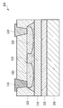
- FIG. 2 is a sectional view of the substrate taken along the line II-II in FIG.
- the GePD 100 of FIG. 1 light input from the waveguide layer 1101 at the left end reaches the Ge layer 114, which is a light absorption layer on the silicon slab 1102, and when the light is absorbed, the electrodes 117 and the electrodes 116 and 118 are formed.
- a photocurrent flows between and detects light.
- the cladding layer 103 and the core layer 110 shown in the cross-sectional view of FIG. 2 are omitted, and the electrodes 116 to 118 are implanted with the first impurity (for example, p-type). Only the positions in contact with the Ge electrode 115 into which the silicon electrodes 112 and 113 and the second impurity (for example, n-type) of the conductivity type opposite to the first impurity are implanted are shown.
- the GePD 100 is formed on a SOI (Silicon On Insulator) substrate including a Si substrate, a Si oxide film, and a surface Si layer by using a lithography technique or the like.
- SOI Silicon On Insulator
- the GePD 100 includes a Si substrate 101, a lower clad layer 102 made of a Si oxide film on the Si substrate, a core layer 110 for guiding signal light, and a light formed on the core layer 110. And a core layer 110 and an upper clad layer 103 formed on the Ge layer 114.
- the core layer 110 of FIG. 2 corresponds to the waveguide layer 1101 and the silicon slab 1102 of FIG.
- a Si slab 111 into which a first impurity is implanted, and silicon electrode portions 112 and 113 which are doped with a high concentration of the first impurity and act as electrodes are formed.
- a Ge layer 114 is stacked by epitaxial growth, and a Ge region 115 doped with a second impurity is formed on the Ge layer 114.
- the Ge layer 114 may be a light absorption layer formed of a germanium compound layer, and is collectively referred to as a germanium layer.
- electrodes 116 to 118 are provided on the silicon electrode portions 112 and 113 and the Ge region 115 so as to be in contact with them, and a photocurrent is detected.
- the lateral Ge PD 100 of FIG. 3 includes a p-type Si slab 111 doped with the first impurity of FIG. 2 and a germanium region 121 doped with the first impurity instead of the Ge region 115 doped with the second impurity.
- a germanium region 122 having a second impurity implanted therein is provided.
- the Ge layer 114 separates the germanium regions 121 and 122, and photocurrent is detected from the electrodes 116 and 118.
- Another lateral GePD 100 of FIG. 4 is a p-type Si slab 111 doped with the first impurity and a Ge region 115 doped with the second impurity of FIG. 2, instead of the silicon region doped with the first impurity.
- the Ge layer 114 is in contact with the core layer 110 across the two silicon regions, and photocurrent is detected from the electrodes 116 and 118.
- the Ge layer 114 can be a light absorption layer formed of a germanium compound layer, and is collectively referred to as a germanium layer.
- a single GePD is rarely used, and generally 2 to 8 GePDs are used side by side. This is because a plurality of PDs are used when a GePD is required for the number of wavelengths in a system that employs wavelength division multiplexing (WDM) that uses multiple wavelengths, or when it is used as a balanced PD in a system that employs optical digital coherent communication technology. I need.
- WDM wavelength division multiplexing
- FIG. 5 shows an example of the configuration of a conventional optical receiver used in the optical digital coherent communication technology.
- the received polarization multiplexed light input to the polarization demultiplexer 901 is polarization-demultiplexed and combined with the two optical hybrids 940 and 941 by the local oscillation light of two different polarizations from the local oscillation light source 900. ..
- Eight GePDs 950A to 950H are used for optoelectric conversion of a total of eight output lights from the two optical hybrids 940 and 941 (four in total).
- the conventional GePD 100 shown in FIGS. 1 to 4 has a problem that the temperature characteristics of optical sensitivity (characteristic of current output with respect to optical input power, unit A/W) are not constant.
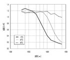
- FIG. 6 is a plot of photoelectric conversion sensitivities to three different temperatures when a reverse bias of 1.6 V is applied in the communication wavelength band C band and L band (wavelength 1530 to 1565 nm, 1565 to 1625 nm) of GePD. It is a figure. For example, at 31° C., the sensitivity is almost constant up to the C band, but the sensitivity decreases at the L band. This change in sensitivity is caused by a change in the optical absorption spectrum of germanium. At ⁇ 5° C., sensitivity tends to decrease even in the C band.
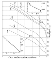
- FIG. 7 shows the temperature dependence of the optical absorption spectrum of germanium itself (see Non-Patent Document 1).
- the band gap of germanium shifts to the high energy side. That is, the light absorption spectrum edge shifts to the short wavelength side.
- the edge of the optical absorption spectrum of germanium used for GePD is 31° C., which is just around 1565 nm on the long wavelength side of the C band. Therefore, even at a temperature of 31° C., even a GePD showing a constant sensitivity in the entire C band, the sensitivity gradually decreases from the long wavelength side as the temperature decreases. This tendency is shown in FIG. 6, and the longer the wavelength, the lower the light sensitivity at -5° C., which is the lower temperature.
- the present invention has been made in view of such a problem, and an object of the present invention is to provide a photodetector using GePD, which suppresses a temperature change and has a small change in photosensitivity. With the goal.
- the present invention is characterized by having the following configuration in order to achieve such an object.
- (Structure 1) A plurality of photodiodes formed on a silicon substrate and having a germanium layer as a light absorption layer, Two integrated circuits arranged in parallel to two sides of one corner of the silicon substrate, Each of the two integrated circuits is connected to two or more of the photodiodes formed on the silicon substrate, The integrated circuit is placed equidistant from each of the photodiodes, The number of said photodiodes corresponding to each said integrated circuit is equal, A photodetector characterized in that
- (Configuration 2) A plurality of photodiodes formed on a silicon substrate and having a germanium layer as a light absorption layer, Two or more integrated circuits monolithically integrated on the silicon substrate, Each of the two or more integrated circuits is connected to the two or more photodiodes formed on the silicon substrate; The integrated circuit is placed equidistant from each of the photodiodes, The number of said photodiodes corresponding to each said integrated circuit is equal, A photodetector characterized in that
- the photodiode is A silicon substrate, A lower clad layer formed on the silicon substrate, A silicon core layer formed on the lower clad layer and including a silicon region doped with a first conductivity type impurity; A silicon waveguide layer connected to the silicon core layer, A germanium layer formed on the silicon core layer and including a region doped with a second conductivity type impurity; An upper clad layer formed on the silicon core layer and the germanium layer, A photodetector comprising electrodes connected to the silicon region and the germanium layer region, respectively.
- the photodiode is A silicon substrate, A lower clad layer formed on the silicon substrate, A silicon core layer formed on the lower clad layer, A silicon waveguide layer connected to the silicon core layer, A germanium layer formed on the silicon core layer and including two germanium regions doped with impurities of different conductivity types; An upper clad layer formed on the silicon core layer and the germanium layer, A photodetector comprising electrodes respectively connected to the two germanium regions of the germanium layer.
- the photodiode is A silicon substrate, A lower clad layer formed on the silicon substrate, A silicon core layer formed on the lower cladding layer and including two silicon regions doped with impurities of different conductivity types; A silicon waveguide layer connected to the silicon core layer, A germanium layer formed over the two silicon regions on the silicon core layer; An upper clad layer formed on the silicon core layer and the germanium layer, An electrode connected to each of the two silicon regions, A photodetector characterized in that
- the integrated circuit includes a heat conductor arranged so as to surround the photodiode to be connected,
- the thermal conductor is a metal or high thermal conductivity material disposed in or on the upper cladding layer,
- the temperature change of the GePD is suppressed by utilizing the heat generation of the integrated circuit, thereby providing the photodetector with little change in the photosensitivity. It becomes possible.
- the silicon photonics photodetector of the present invention at least two integrated circuits are arranged to surround at least one corner of a silicon photonics silicon substrate chip, or are monolithically integrated on the silicon substrate. It On the chip side of silicon photonics, a plurality of GePD groups including a plurality of GePDs are arranged as photodetecting elements, the integrated circuit and each GePD are arranged at equal distances, and are wired by electrodes. It is desirable that the number of equidistantly arranged GePDs corresponding to each integrated circuit is equal.
- the integrated circuit is a circuit that generates heat, such as a transimpedance amplifier or driver having multiple channels, a digital signal processor, or the like.
- the GePD heat generated from the integrated circuit is applied to the GePD, so that the GePD can be warmed and sensitivity deterioration can be prevented.
- the type of GePD may be any of the vertical type and the horizontal type described in FIGS.
- FIG. 8 is a typical arrangement example of the photodetectors according to the first embodiment of the present invention.
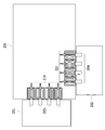
- the integrated circuits 201 and 202 are arranged so as to surround one corner of the silicon photonics chip 200 in which two GePD groups 210211 are arranged at one corner.
- a GePD group 210 is arranged in the integrated circuit 201, and a GePD group 211 is arranged in the integrated circuit 202 so as to correspond to each other, and the GePDs in each GePD group are arranged so as to be equidistant from each integrated circuit.
- the integrated circuits when a plurality of GePDs are arranged, most of the integrated circuits have multiple channels or operate differentially.
- a transimpedance amplifier that differentially operates for 2 channels is integrated.
- the arrangement is the same as in the case of the circuits 201 and 202.
- the wiring connecting the integrated circuits 201 and 202 and the GePD groups 210 and 211 may be wire bonding or flip chip connection using metal bumps.
- the integrated circuits 201 and 202 are heat sources, and the heat generated by these is transmitted to the GePD groups 210 and 211 through this connection wiring.
- one GePD group is arranged on one side of one square chip 200. Therefore, there is only one integrated circuit 201 that serves as a heat source, and the temperature distribution due to the diffused heat is also the temperature distribution 220 in FIG. 9.
- the heat distribution due to heat diffusion is two, that is, the temperature distribution 220 and 221. Yes, and heat is generated so as to surround the arrangement of the GePD. Therefore, heat is efficiently concentrated on the corners of the chip 200.
- the heat of the integrated circuits 201 and 202 can be efficiently applied to the GePD group. Due to this heat, the GePD group is warmed and the sensitivity is not lowered.
- the present invention makes it possible to heat the GePD more efficiently than in the conventional arrangement, simply by changing the arrangement of the integrated circuit without the need for additional circuitry.
- FIG. 11 is a diagram showing the configuration of the second embodiment of the present invention.
- the second embodiment is an example in which integrated circuits 201 and 202 are monolithically integrated on the silicon substrate of the silicon photonics chip 200.
- the GePD group is arranged on the silicon photonics chip 200 so as to be surrounded by monolithically integrated integrated circuits 201 and 202.
- the GePD group 210 is arranged in the integrated circuit 201, and the GePD group 211 is arranged in the integrated circuit 202 so as to be equidistant from each integrated circuit. Since the integrated circuits 201 and 202 are monolithically integrated, the number of integrated circuits 201 and 202 need not be two, and may be three or more.
- an embodiment having three or more integrated circuits is possible, such as another configuration of Embodiment 2 shown in FIG.
- four integrated circuits 201, 202, 251, 252 are arranged so as to surround the GePD groups 210, 211 arranged in the center of the silicon photonics chip 200 so as to form electric wiring in four directions.
- the structure gives heat.
- the distances between the GePDs of the GePD groups 210 and 211 and the four integrated circuits 201, 202, 251, 252 are equal so that the heat given from each integrated circuit is uniform.
- the wiring connecting the integrated circuits 201, 202, 251, 252 and the GePD groups 210, 211 is the metal wired in the upper cladding layer 103. Since they are monolithically integrated, the heat from the four integrated circuits 201, 202, 251, 252, which are heat sources, is transmitted to each GePD not only as a metal wiring but also as a substrate through a conduction path.
- FIG. 13 is a diagram showing the configuration of the third embodiment of the present invention.
- the heat conductors 212 and 213 are wired from the integrated circuits 201 and 202, and serve as a heat pump that transfers heat from the integrated circuits.
- the thermal conductors 212, 213 can be metal or high thermal conductivity material wired in or on the upper cladding layer 103 and have sufficient thermal conductivity and thickness or width to ensure the desired thermal conductivity.
- the wiring can have.
- the heat conductors 212 and 213 are arranged so as to surround the GePD groups.
- FIG. 14 is a diagram showing the configuration of the fourth embodiment of the present invention.
- the fourth embodiment is an example in which heaters 221 to 228 are arranged in addition to the arrangement of the first embodiment. This is an example in which a heater for providing auxiliary heat is arranged when the heat from the integrated circuits 201 and 202 alone is insufficient to heat the GePD groups 210 and 211.
- the heaters 221 to 228 of Example 4 are regions of the resistors that cover the germanium layer of each GePD in the configuration of FIG. 14, and are formed in the upper cladding layer 103 of the GePD as shown in the substrate cross-sectional view of FIG.
- the heater 130 may be made of metal or a metal compound wired.
- the heaters 221 to 228 of the fourth embodiment are regions of the linear resistor surrounding the germanium layer of each GePD in the configuration of FIG. 15, and as shown in the substrate cross-sectional view of FIG. It is also possible to configure the heater 131 including a linear conductive region produced by adding impurities to the heater 131.
- the temperature change of the GePD is suppressed by utilizing the heat generation of the integrated circuit, thereby providing the photodetector with little change in the photosensitivity. It becomes possible.
- Germanium photodetector 101 silicon (Si) substrate 102 lower clad layer 103 upper clad layer 110 (silicon) core layer 111, p-type Si slabs 112 and 113, p++Si electrode part 114, germanium (Ge) layer 115, n-type germanium (Ge) region 116 117, 118, electrodes 121 p-type germanium region 122 n-type germanium region 123 region 124p p-type silicon region 124n n-type silicon region 125 silicon electrode portion 1101 waveguide layer 1102 silicon slab 130, 131, 221-228 resistor (heater ) 200 Silicon photonics chip 201, 202, 251, 252 Integrated circuit 210, 211 GePD group 220, 221 Temperature distribution 212, 213 Thermal conductor 900 Local light source 901 Polarization splitter 940, 941 Optical hybrid
Landscapes
- Light Receiving Elements (AREA)
- Optical Integrated Circuits (AREA)
Abstract
GePDを用いた光検出器において、温度による光感度の変化の少ない光検出器を提供する。シリコン基板上に形成され、ゲルマニウム、またはゲルマニウム化合物を光吸収層に持つ複数のフォトダイオードと、前記シリコン基板の1つの隅に関わる2辺に対し、各々平行に配置される集積回路のチップを2つ備え、前記2つの集積回路は、前記シリコン基板上に形成されたフォトダイオードと接続され、前記一つの隅に関わる一辺に対して平行な前記集積回路に対し、前記フォトダイオードは2つ以上が等距離に配置され、前記各集積回路から見た、等距離に配置される前記フォトダイオードの数は等しい、ことを特徴とする光検出器とした。
Description
本発明は、光通信システムや光情報処理システムにおいて用いられる光検出器に関し、特に光感度の温度依存性が小さい、光検出器を提供するための構造に関するものである。
近年の光通信の普及に伴い、光通信装置の低コスト化が求められている。その解決策の1つとして、光通信装置を構成する光回路を、シリコンウエハのような大口径ウエハ上に、シリコンフォトニクスのような微小光回路技術を用いて一度に多数形成する方法がある。これにより、1チップあたりの材料費を劇的に下げ、光通信装置の低コスト化を図ることが出来る。
このような技術を用いたシリコン(Si)基板上に形成する代表的な光検出器としては、モノリシック集積が可能なゲルマニウム光検出器(GePD)がある。
図1は、従来の導波路結合型の縦型GePD100の構造を模式的に示す図である。図2は、図1のII-IIの基板断面図である。図1のGePD100は概略、左端の導波路層1101から入力された光が、シリコンスラブ1102上の光吸収層であるGe層114に達し、光が吸収されると電極117と電極116、118との間に光電流が流れ、光を検出する。
尚、構造を分かり易くするために、図1では、図2の断面図に示すクラッド層103、コア層110を省いており、電極116~118が、第一の不純物(例えばp型)をインプラしたシリコン電極部112、113および第一の不純物と反対の導電型の第二の不純物(例えばn型)をインプラしたGe領域115に接する位置のみを、表示している。GePD100は、Si基板、Si酸化膜、表面Si層からなるSOI(Silicon On Insulator)基板にリソグラフィ技術等を用いて形成される。
図2の基板断面図においてGePD100は、Si基板101と、Si基板上のSi酸化膜からなる下部クラッド層102と、信号光を導くコア層110と、コア層110上に形成された光を吸収するGe層114と、コア層110およびGe層114上に形成された上部クラッド層103を備える。図2のコア層110は、図1の導波路層1101とシリコンスラブ1102に対応する。
図2のコア層110の上には、第一の不純物をインプラしたSiスラブ111、および第一の不純物が高濃度にドーピングされ、電極として作用するシリコン電極部112、113が形成されている。両電極部112、113の間のSiスラブ111の上には、Ge層114がエピタキシャル成長によって積層され、その上部に第二の不純物がドーピングされたGe領域115が形成されている。Ge層114は、ゲルマニウム化合物の層で形成された光吸収層であることも可能であり、ゲルマニウム層と総称する。そして、シリコン電極部112、113およびGe領域115の上には、それらに接するように電極116~118を備え、光電流が検出される。
GePDは、導波路層1101からシリコンスラブ1102に光が入射されてGe層114で光が吸収されると、電極117と電極116、118との間に光電流が流れるので、その電流を検出することで光を検出する。
図3、4に示すような、横型のGePDも従来より存在する。図3の横型のGePD100は、図2の第一の不純物をインプラしたp型Siスラブ111、第二の不純物がドーピングされたGe領域115の代わりに、第一の不純物をインプラしたゲルマニウム領域121と第二の不純物をインプラしたゲルマニウム領域122を備える。ゲルマニウム領域121と122の間は、Ge層114で分離されており、光電流は電極116、118から検出される。
図4の別の横型のGePD100は、図2の第一の不純物をインプラしたp型Siスラブ111、第二の不純物がドーピングされたGe領域115の代わりに、第一の不純物をインプラしたシリコン領域124pと第二の不純物をインプラしたシリコン領域124n、および第二の不純物が高濃度にドーピングされ、電極として作用するシリコン電極部125を備える。シリコン領域124pとシリコン領域124nの間の領域123では、Ge層114が2つのシリコン領域に跨ってコア層110と接しており、光電流は電極116、118から検出される。いずれの横型のGePDにおいても、Ge層114はゲルマニウム化合物の層で形成された光吸収層であることも可能であり、ゲルマニウム層と総称する。
また、GePDを用いた光通信システムや光情報処理システムでは、単独のGePDを使うことは少なく、一般に2~8個程度のGePDを並べて使う。これは多波長を使う波長分割多重方式(WDM)を採用するシステムにおいて波長の数だけGePDを必要とする場合や、光デジタルコヒーレント通信技術を採用するシステムにおいてバランスPDとして使う場合に複数のPDを必要とする。
図5は、光デジタルコヒーレント通信技術において用いる従来の光受信機の構成の一例である。この構成では、偏波分離器901に入力された受信偏波多重光が偏波分離され、2つの光ハイブリッド940、941において、局発光源900からの2つの異なる偏波の局発光と組み合わされる。2つの光ハイブリッド940、941からの、各4つ、計8つの出力光の光電気変換のために、8個のGePD950A~950Hが用いられる。
G.G.Macfarlane, T.P. McLean, J.E. Quarrington and V. Roberts, "Fine Structure in the Absorption-Edge Spectrum of Ge",Phys. Rev. 108, 6 (1957) 1377-1383.
しかしながら、図1~4に示す従来のGePD100は、光感度(光入力パワーに対する電流出力の特性、単位A/W)の温度特性が一定ではないという課題がある。
図6は、GePDの通信波長帯域C帯、L帯(波長1530~1565nm、1565~1625nm)で、逆バイアス1.6Vを印加した時の、3通りの温度に対する光電気変換の感度をプロットした図である。例えば31℃ではC帯付近まではほぼ一定の感度を示すが、L帯になると感度を落とす。この感度の変化はゲルマニウムの光吸収スペクトルの変化によってもたらされている。-5℃になるとC帯においても感度を落とす傾向を示す。
図7は、ゲルマニウム自身の光吸収スペクトルの温度依存性である(非特許文献1参照)。温度が低温になるとゲルマニウムのバンドギャップは高エネルギー側にシフトする。すなわち光吸収スペクトル端は短波長側にシフトする。GePDに用いているゲルマニウムの光吸収スペクトル端は31℃でちょうどC帯の長波長側の1565nm付近にある。従って31℃ではC帯全域に一定の感度を示すGePDであっても、温度が低くなるにつれ、長波長側から徐々に感度が落ちてゆく。この傾向を示したのが図6であり、長波長ほど低温である-5℃において光感度を落とす傾向がある。
本発明はこのような問題に鑑みてなされたもので、その目的とするところは、GePDを用いた光検出器において、温度変化を抑えることで光感度の変化の少ない光検出器を提供することを目的とする。
本発明は、このような目的を達成するために、以下のような構成を備えることを特徴とする。
(構成1)
シリコン基板の上に形成され、ゲルマニウム層を光吸収層に持つ複数のフォトダイオードと、
前記シリコン基板の1つの隅に関わる2辺に対し、各々平行に配置された集積回路を2つ備え、
2つの前記集積回路は各々、前記シリコン基板の上に形成された2つ以上の前記フォトダイオードと接続され、
前記集積回路は、各前記フォトダイオードと等距離に配置され、
各前記集積回路に対応する前記フォトダイオードの数は等しい、
ことを特徴とする光検出器。
シリコン基板の上に形成され、ゲルマニウム層を光吸収層に持つ複数のフォトダイオードと、
前記シリコン基板の1つの隅に関わる2辺に対し、各々平行に配置された集積回路を2つ備え、
2つの前記集積回路は各々、前記シリコン基板の上に形成された2つ以上の前記フォトダイオードと接続され、
前記集積回路は、各前記フォトダイオードと等距離に配置され、
各前記集積回路に対応する前記フォトダイオードの数は等しい、
ことを特徴とする光検出器。
(構成2)
シリコン基板の上に形成され、ゲルマニウム層を光吸収層に持つ複数のフォトダイオードと、
前記シリコン基板にモノリシック集積された集積回路を2つ以上備え、
2つ以上の前記集積回路は各々、前記シリコン基板の上に形成された2つ以上の前記フォトダイオードと接続され、
前記集積回路は、各前記フォトダイオードと等距離に配置され、
各前記集積回路に対応する前記フォトダイオードの数は等しい、
ことを特徴とする光検出器。
シリコン基板の上に形成され、ゲルマニウム層を光吸収層に持つ複数のフォトダイオードと、
前記シリコン基板にモノリシック集積された集積回路を2つ以上備え、
2つ以上の前記集積回路は各々、前記シリコン基板の上に形成された2つ以上の前記フォトダイオードと接続され、
前記集積回路は、各前記フォトダイオードと等距離に配置され、
各前記集積回路に対応する前記フォトダイオードの数は等しい、
ことを特徴とする光検出器。
(構成3)
構成1または2に記載の光検出器において、前記フォトダイオードは、
シリコン基板と、
前記シリコン基板の上に形成された下部クラッド層と、
前記下部クラッド層の上に形成され、第一の導電型不純物がドーピングされたシリコン領域を含むシリコンコア層と、
前記シリコンコア層に接続されたシリコン導波路層と、
前記シリコンコア層の上に形成され、第二の導電型不純物がドーピングされた領域を含むゲルマニウム層と、
前記シリコンコア層および前記ゲルマニウム層の上に形成された上部クラッド層と、
前記シリコン領域および前記ゲルマニウム層の領域にそれぞれ接続された電極を備える
ことを特徴とする光検出器。
構成1または2に記載の光検出器において、前記フォトダイオードは、
シリコン基板と、
前記シリコン基板の上に形成された下部クラッド層と、
前記下部クラッド層の上に形成され、第一の導電型不純物がドーピングされたシリコン領域を含むシリコンコア層と、
前記シリコンコア層に接続されたシリコン導波路層と、
前記シリコンコア層の上に形成され、第二の導電型不純物がドーピングされた領域を含むゲルマニウム層と、
前記シリコンコア層および前記ゲルマニウム層の上に形成された上部クラッド層と、
前記シリコン領域および前記ゲルマニウム層の領域にそれぞれ接続された電極を備える
ことを特徴とする光検出器。
(構成4)
構成1または2に記載の光検出器において、前記フォトダイオードは、
シリコン基板と、
前記シリコン基板の上に形成された下部クラッド層と、
前記下部クラッド層の上に形成されたシリコンコア層と、
前記シリコンコア層に接続されたシリコン導波路層と、
前記シリコンコア層の上に形成され、異なる導電型不純物がドーピングされた2つのゲルマニウム領域を含むゲルマニウム層と、
前記シリコンコア層および前記ゲルマニウム層の上に形成された上部クラッド層と、
前記ゲルマニウム層の2つの前記ゲルマニウム領域にそれぞれ接続された電極を備える
ことを特徴とする光検出器。
構成1または2に記載の光検出器において、前記フォトダイオードは、
シリコン基板と、
前記シリコン基板の上に形成された下部クラッド層と、
前記下部クラッド層の上に形成されたシリコンコア層と、
前記シリコンコア層に接続されたシリコン導波路層と、
前記シリコンコア層の上に形成され、異なる導電型不純物がドーピングされた2つのゲルマニウム領域を含むゲルマニウム層と、
前記シリコンコア層および前記ゲルマニウム層の上に形成された上部クラッド層と、
前記ゲルマニウム層の2つの前記ゲルマニウム領域にそれぞれ接続された電極を備える
ことを特徴とする光検出器。
(構成5)
構成1または2に記載の光検出器において、前記フォトダイオードは、
シリコン基板と、
前記シリコン基板の上に形成された下部クラッド層と、
前記下部クラッド層の上に形成され、異なる導電型不純物がドーピングされた2つのシリコン領域を含むシリコンコア層と、
前記シリコンコア層に接続されたシリコン導波路層と、
前記シリコンコア層の上に2つの前記シリコン領域に跨って形成されたゲルマニウム層と、
前記シリコンコア層および前記ゲルマニウム層の上に形成された上部クラッド層と、
2つの前記シリコン領域にそれぞれ接続された電極を備える、
ことを特徴とする光検出器。
構成1または2に記載の光検出器において、前記フォトダイオードは、
シリコン基板と、
前記シリコン基板の上に形成された下部クラッド層と、
前記下部クラッド層の上に形成され、異なる導電型不純物がドーピングされた2つのシリコン領域を含むシリコンコア層と、
前記シリコンコア層に接続されたシリコン導波路層と、
前記シリコンコア層の上に2つの前記シリコン領域に跨って形成されたゲルマニウム層と、
前記シリコンコア層および前記ゲルマニウム層の上に形成された上部クラッド層と、
2つの前記シリコン領域にそれぞれ接続された電極を備える、
ことを特徴とする光検出器。
(構成6)
構成1または2に記載の光検出器において、前記集積回路は、前記接続するフォトダイオードを囲うように配置した熱伝導体を備え、
前記熱伝導体は上部クラッド層の中、または上に配置されている金属または高熱伝導材料である、
ことを特徴とする光検出器。
構成1または2に記載の光検出器において、前記集積回路は、前記接続するフォトダイオードを囲うように配置した熱伝導体を備え、
前記熱伝導体は上部クラッド層の中、または上に配置されている金属または高熱伝導材料である、
ことを特徴とする光検出器。
(構成7)
構成3ないし5のいずれか1項に記載の光検出器において、前記フォトダイオードは、
前記ゲルマニウム層に熱を与えるためのヒータを備え、
前記ヒータは前記上部クラッド層の中、または上に配置されている、
ことを特徴とする光検出器。
構成3ないし5のいずれか1項に記載の光検出器において、前記フォトダイオードは、
前記ゲルマニウム層に熱を与えるためのヒータを備え、
前記ヒータは前記上部クラッド層の中、または上に配置されている、
ことを特徴とする光検出器。
(構成8)
構成3ないし5のいずれか1項に記載の光検出器において、前記フォトダイオードは、
前記ゲルマニウム層に熱を与えるためのヒータを備え、
前記ヒータは前記シリコンコア層の上部に形成された線状の導電性領域である、
ことを特徴とする光検出器。
構成3ないし5のいずれか1項に記載の光検出器において、前記フォトダイオードは、
前記ゲルマニウム層に熱を与えるためのヒータを備え、
前記ヒータは前記シリコンコア層の上部に形成された線状の導電性領域である、
ことを特徴とする光検出器。
以上記載したように、本発明によれば、GePDを用いた光検出器において、集積回路の発熱を利用してGePDの温度変化を抑えることで、光感度の変化の少ない光検出器を提供することが可能となる。
本発明のシリコンフォトニクスによる光検出器では、少なくとも2つの集積回路が、シリコンフォトニクスのシリコン基板のチップの少なくとも1つの隅(角)を囲うように配置されるか、またはシリコン基板上にモノリシック集積される。シリコンフォトニクスによるチップ側には、光検出素子として複数のGePDを含むGePD群が複数配置され、集積回路と各GePDが等距離で配置され、電極で配線される。各集積回路に対応する、等距離に配置されるGePDの数は等しいことが望ましい。集積回路は、例えば多chを備えたトランスインピーダンスアンプやドライバ、デジタルシグナルプロセッサなどの、発熱する回路である。
本発明に係る光検出器においては、集積回路から発する熱をGePDに与える事で、GePDを温め、感度の劣化を防ぐことが出来る。GePDのタイプは、図1から4に記載した縦型、横型のいずれのタイプであってもよい。
以下、図面を参照しながら本発明の実施形態について詳細に説明する。
(実施例1)
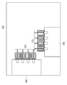
図8は本発明の実施例1の光検出器の典型的な配置例である。本発明の光検出器では、一つの隅に2つのGePD群210211が配置されたシリコンフォトニクスチップ200の一つの隅において、集積回路201と202が囲うように配置される。集積回路201にはGePD群210が、集積回路202にはGePD群211が対応するように配置され、各GePD群のGePDが各集積回路から等距離になるように配置される。
図8は本発明の実施例1の光検出器の典型的な配置例である。本発明の光検出器では、一つの隅に2つのGePD群210211が配置されたシリコンフォトニクスチップ200の一つの隅において、集積回路201と202が囲うように配置される。集積回路201にはGePD群210が、集積回路202にはGePD群211が対応するように配置され、各GePD群のGePDが各集積回路から等距離になるように配置される。
一般に複数のGePDが配置されるときは、集積回路が多chの場合か、差動動作する場合が殆どであり、例えば本実施例1で言えば、2chの差動動作するトランスインピーダンスアンプが集積回路201、202であった場合の配置と同等となる。集積回路201、202とGePD群210、211を繋ぐ配線は、ワイヤボンディングでも金属バンプを使ったフリップチップ接続でも良い。集積回路201、202は熱源であり、これらの発する熱は、この接続配線を伝ってGePD群210、211に伝わる。
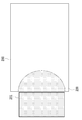
従来の一般的な光検出器の配置では、四角い一つのチップ200の1辺に対して、1つのGePD群が並ぶ。そのため、熱源となる集積回路201も一つであり、拡散する熱による温度の分布も図9の温度分布220のようになる。
対して本発明の光検出器の配置では、図10の様にGePD群に対応して熱源となる2つの集積回路201と202があり、熱拡散による熱分布も温度分布220と221で二つあり、なおかつGePDの配置に対して囲うように熱が発生する。そのため熱がチップ200の隅に効率的に集中する。この隅にGePD群210と211を配置することで、集積回路201および202の熱を効率的にGePD群に与える事が出来る。この熱によってGePD群は温められ、感度を落とすことが無くなる。本発明は集積回路の配置を変えるだけで、追加の回路を必要とせず、従来の配置より効率的にGePDに熱を与える事が可能となる。
(実施例2)
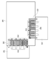
図11は、本発明の実施例2の構成を示す図である。実施例2は、シリコンフォトニクスチップ200のシリコン基板の上に、集積回路201、202がモノリシック集積された例である。GePD群はシリコンフォトニクスチップ200の上で、モノリシック集積された集積回路201と202によって囲われるように配置される。集積回路201にはGePD群210が、集積回路202にはGePD群211が各集積回路から等距離になるように配置される。集積回路201、202はモノリシック集積されているため、2つである必要は無く、3つ以上の集積回路が有っても良い。
図11は、本発明の実施例2の構成を示す図である。実施例2は、シリコンフォトニクスチップ200のシリコン基板の上に、集積回路201、202がモノリシック集積された例である。GePD群はシリコンフォトニクスチップ200の上で、モノリシック集積された集積回路201と202によって囲われるように配置される。集積回路201にはGePD群210が、集積回路202にはGePD群211が各集積回路から等距離になるように配置される。集積回路201、202はモノリシック集積されているため、2つである必要は無く、3つ以上の集積回路が有っても良い。
例えば図12に示す実施例2の別構成の様に、3つ以上の集積回路が有る実施例も可能である。図12では、シリコンフォトニクスチップ200の中央に電気配線を四方に出す形で配置されたGePD群210、211に対して、これらを囲うように4つの集積回路201、202、251、252が配置され、熱を与える構造になる。各集積回路から与えられる熱が均一となるように、GePD群210、211の各GePDと4つの集積回路201、202、251、252の間の距離は等距離とされる。
集積回路201、202、251、252とGePD群210、211を繋ぐ配線は、上部クラッド層103の中に配線された金属である。モノリシック集積しているため、熱源である4つの集積回路201、202、251、252からの熱は、金属配線だけではなく、基板も伝導パスとして、各GePDに伝わる。
逆に、シリコンフォトニクスチップの中央に、1つのあるいは任意の複数の集積回路が配置され、これを囲うように周囲に配置された任意の複数のGePD群に熱を与える構造とすることもできる。
(実施例3)
図13は、本発明の実施例3の構成を示す図である。実施例1の配置に加えて、電気配線以外の熱伝導体212、213を追加した例である。熱伝導体212、213は、集積回路201、202から配線されており、集積回路からの熱を伝えるヒートポンプの役割を果たす。熱伝導体212、213は、上部クラッド層103の中または上に配線された金属または高熱伝導材料であることができ、所望の熱伝導を確保するために充分な熱伝導率と厚みまたは幅を有する配線とすることができる。実施例3では、GePD群210、211に、集積回路201、202が発する熱を加える事が主目的であるため、熱伝導体212、213はGePD群を囲うように配置される。
図13は、本発明の実施例3の構成を示す図である。実施例1の配置に加えて、電気配線以外の熱伝導体212、213を追加した例である。熱伝導体212、213は、集積回路201、202から配線されており、集積回路からの熱を伝えるヒートポンプの役割を果たす。熱伝導体212、213は、上部クラッド層103の中または上に配線された金属または高熱伝導材料であることができ、所望の熱伝導を確保するために充分な熱伝導率と厚みまたは幅を有する配線とすることができる。実施例3では、GePD群210、211に、集積回路201、202が発する熱を加える事が主目的であるため、熱伝導体212、213はGePD群を囲うように配置される。
(実施例4)
図14は、本発明の実施例4の構成を示す図である。実施例4は、実施例1の配置に加えて、ヒータ221~228を配置した例である。集積回路201、202からの熱だけではGePD群210、211を加熱するのに不十分だった場合に、補助的な熱を与えるためのヒータを配置した実施例である。
図14は、本発明の実施例4の構成を示す図である。実施例4は、実施例1の配置に加えて、ヒータ221~228を配置した例である。集積回路201、202からの熱だけではGePD群210、211を加熱するのに不十分だった場合に、補助的な熱を与えるためのヒータを配置した実施例である。
実施例4のヒータ221~228は、図14の構成では各GePDのゲルマニウム層を覆う抵抗体の領域であって、図16の基板断面図に示す様に、GePDの上部クラッド層103の中に配線された金属または金属化合物からなるヒータ130で構成することができる。
また、実施例4のヒータ221~228は、図15の構成では各GePDのゲルマニウム層を囲う線状抵抗体の領域であって、図17の基板断面図に示す様に、GePDのコア層110に不純物を添加して作製した線状の導電性領域からなるヒータ131として構成することもできる。
以上記載したように、本発明によれば、GePDを用いた光検出器において、集積回路の発熱を利用してGePDの温度変化を抑えることで、光感度の変化の少ない光検出器を提供することが可能となる。
100、950A~950H ゲルマニウム光検出器(GePD)
101 シリコン(Si)基板
102 下部クラッド層
103 上部クラッド層
110 (シリコン)コア層
111、 p型Siスラブ
112、113、 p++Si電極部
114、 ゲルマニウム(Ge)層
115、 n型ゲルマニウム(Ge)領域
116、117、118、 電極
121 p型ゲルマニウム領域
122 n型ゲルマニウム領域
123 領域
124p p型シリコン領域
124n n型シリコン領域
125 シリコン電極部
1101 導波路層
1102 シリコンスラブ
130、131、221~228 抵抗体(ヒータ)
200 シリコンフォトニクスチップ
201、202、251、252 集積回路
210、211 GePD群
220、221 温度分布
212、213 熱伝導体
900 局発光源
901 偏波分離器
940、941 光ハイブリッド
101 シリコン(Si)基板
102 下部クラッド層
103 上部クラッド層
110 (シリコン)コア層
111、 p型Siスラブ
112、113、 p++Si電極部
114、 ゲルマニウム(Ge)層
115、 n型ゲルマニウム(Ge)領域
116、117、118、 電極
121 p型ゲルマニウム領域
122 n型ゲルマニウム領域
123 領域
124p p型シリコン領域
124n n型シリコン領域
125 シリコン電極部
1101 導波路層
1102 シリコンスラブ
130、131、221~228 抵抗体(ヒータ)
200 シリコンフォトニクスチップ
201、202、251、252 集積回路
210、211 GePD群
220、221 温度分布
212、213 熱伝導体
900 局発光源
901 偏波分離器
940、941 光ハイブリッド
Claims (8)
- シリコン基板の上に形成され、ゲルマニウム層を光吸収層に持つ複数のフォトダイオードと、
前記シリコン基板の1つの隅に関わる2辺に対し、各々平行に配置された集積回路を2つ備え、
2つの前記集積回路は各々、前記シリコン基板の上に形成された2つ以上の前記フォトダイオードと接続され、
前記集積回路は、各前記フォトダイオードと等距離に配置され、
各前記集積回路に対応する前記フォトダイオードの数は等しい、
ことを特徴とする光検出器。 - シリコン基板の上に形成され、ゲルマニウム層を光吸収層に持つ複数のフォトダイオードと、
前記シリコン基板にモノリシック集積された集積回路を2つ以上備え、
2つ以上の前記集積回路は各々、前記シリコン基板の上に形成された2つ以上の前記フォトダイオードと接続され、
前記集積回路は、各前記フォトダイオードと等距離に配置され、
各前記集積回路に対応する前記フォトダイオードの数は等しい、
ことを特徴とする光検出器。 - 請求項1または2に記載の光検出器において、前記フォトダイオードは、
シリコン基板と、
前記シリコン基板の上に形成された下部クラッド層と、
前記下部クラッド層の上に形成され、第一の導電型不純物がドーピングされたシリコン領域を含むシリコンコア層と、
前記シリコンコア層に接続されたシリコン導波路層と、
前記シリコンコア層の上に形成され、第二の導電型不純物がドーピングされた領域を含むゲルマニウム層と、
前記シリコンコア層および前記ゲルマニウム層の上に形成された上部クラッド層と、
前記シリコン領域および前記ゲルマニウム層の領域にそれぞれ接続された電極を備える
ことを特徴とする光検出器。 - 請求項1または2に記載の光検出器において、前記フォトダイオードは、
シリコン基板と、
前記シリコン基板の上に形成された下部クラッド層と、
前記下部クラッド層の上に形成されたシリコンコア層と、
前記シリコンコア層に接続されたシリコン導波路層と、
前記シリコンコア層の上に形成され、異なる導電型不純物がドーピングされた2つのゲルマニウム領域を含むゲルマニウム層と、
前記シリコンコア層および前記ゲルマニウム層の上に形成された上部クラッド層と、
前記ゲルマニウム層の2つの前記ゲルマニウム領域にそれぞれ接続された電極を備える
ことを特徴とする光検出器。 - 請求項1または2に記載の光検出器において、前記フォトダイオードは、
シリコン基板と、
前記シリコン基板の上に形成された下部クラッド層と、
前記下部クラッド層の上に形成され、異なる導電型不純物がドーピングされた2つのシリコン領域を含むシリコンコア層と、
前記シリコンコア層に接続されたシリコン導波路層と、
前記シリコンコア層の上に2つの前記シリコン領域に跨って形成されたゲルマニウム層と、
前記シリコンコア層および前記ゲルマニウム層の上に形成された上部クラッド層と、
2つの前記シリコン領域にそれぞれ接続された電極を備える、
ことを特徴とする光検出器。 - 請求項1または2に記載の光検出器において、前記集積回路は、前記接続するフォトダイオードを囲うように配置した熱伝導体を備え、
前記熱伝導体は上部クラッド層の中、または上に配置されている金属または高熱伝導材料である、
ことを特徴とする光検出器。 - 請求項3ないし5のいずれか1項に記載の光検出器において、前記フォトダイオードは、
前記ゲルマニウム層に熱を与えるためのヒータを備え、
前記ヒータは前記上部クラッド層の中、または上に配置されている、
ことを特徴とする光検出器。 - 請求項3ないし5のいずれか1項に記載の光検出器において、前記フォトダイオードは、
前記ゲルマニウム層に熱を与えるためのヒータを備え、
前記ヒータは前記シリコンコア層の上部に形成された線状の導電性領域である、
ことを特徴とする光検出器。
Priority Applications (1)
| Application Number | Priority Date | Filing Date | Title |
|---|---|---|---|
| US17/422,396 US11887999B2 (en) | 2019-01-17 | 2020-01-15 | Photodetector |
Applications Claiming Priority (2)
| Application Number | Priority Date | Filing Date | Title |
|---|---|---|---|
| JP2019005933A JP7181462B2 (ja) | 2019-01-17 | 2019-01-17 | 光検出器 |
| JP2019-005933 | 2019-01-17 |
Publications (1)
| Publication Number | Publication Date |
|---|---|
| WO2020149309A1 true WO2020149309A1 (ja) | 2020-07-23 |
Family
ID=71613152
Family Applications (1)
| Application Number | Title | Priority Date | Filing Date |
|---|---|---|---|
| PCT/JP2020/001093 Ceased WO2020149309A1 (ja) | 2019-01-17 | 2020-01-15 | 光検出器 |
Country Status (3)
| Country | Link |
|---|---|
| US (1) | US11887999B2 (ja) |
| JP (1) | JP7181462B2 (ja) |
| WO (1) | WO2020149309A1 (ja) |
Families Citing this family (1)
| Publication number | Priority date | Publication date | Assignee | Title |
|---|---|---|---|---|
| US12298560B2 (en) * | 2021-11-10 | 2025-05-13 | Intel Corporation | Germanium waveguide photodetector with integrated heater |
Citations (8)
| Publication number | Priority date | Publication date | Assignee | Title |
|---|---|---|---|---|
| JPS63205949A (ja) * | 1987-02-23 | 1988-08-25 | Sony Corp | 半導体装置 |
| JP2002101051A (ja) * | 2000-09-21 | 2002-04-05 | Hitachi Ltd | 波長多重光インタコネクション装置 |
| WO2010113968A1 (ja) * | 2009-03-30 | 2010-10-07 | 京セラ株式会社 | 光電気配線基板および光モジュール |
| WO2010143672A1 (ja) * | 2009-06-09 | 2010-12-16 | 日本電気株式会社 | 治具、パッケージ、システム基板および素子搭載方法 |
| JP2012518202A (ja) * | 2009-02-17 | 2012-08-09 | オクラロ テクノロジー リミテッド | 光通信用の光チップおよび光デバイス |
| US20150243800A1 (en) * | 2014-02-21 | 2015-08-27 | Sifotonics Technologies Co., Ltd. | Ge/Si Avalanche Photodiode With Integrated Heater And Fabrication Thereof |
| JP2018074104A (ja) * | 2016-11-04 | 2018-05-10 | 日本電信電話株式会社 | 光検出器 |
| JP2018082089A (ja) * | 2016-11-17 | 2018-05-24 | 日本電信電話株式会社 | 光検出器 |
Family Cites Families (9)
| Publication number | Priority date | Publication date | Assignee | Title |
|---|---|---|---|---|
| US8067687B2 (en) * | 2002-05-21 | 2011-11-29 | Alliance For Sustainable Energy, Llc | High-efficiency, monolithic, multi-bandgap, tandem photovoltaic energy converters |
| US7615731B2 (en) * | 2006-09-14 | 2009-11-10 | Carestream Health, Inc. | High fill-factor sensor with reduced coupling |
| US7820525B2 (en) * | 2009-03-25 | 2010-10-26 | E-Phocus | Method for manufacturing hybrid image sensors |
| KR101736321B1 (ko) * | 2010-12-22 | 2017-05-17 | 삼성디스플레이 주식회사 | 엑스레이 검출기용 박막 트랜지스터 어레이 기판 및 엑스레이 검출기 |
| WO2013130038A1 (en) * | 2012-02-28 | 2013-09-06 | Carestream Health, Inc. | Radiographic detector arrays including scintillators and methods for same |
| JP5925711B2 (ja) * | 2013-02-20 | 2016-05-25 | 浜松ホトニクス株式会社 | 検出器、pet装置及びx線ct装置 |
| JP2015164284A (ja) * | 2014-01-28 | 2015-09-10 | キヤノン株式会社 | 固体撮像素子、動き情報取得装置、および撮像装置 |
| TWI723890B (zh) * | 2015-08-04 | 2021-04-01 | 光澄科技股份有限公司 | 製造影像感測陣列之方法 |
| CN107248518B (zh) * | 2017-05-26 | 2020-04-17 | 京东方科技集团股份有限公司 | 光电传感器及其制作方法、显示装置 |
-
2019
- 2019-01-17 JP JP2019005933A patent/JP7181462B2/ja active Active
-
2020
- 2020-01-15 US US17/422,396 patent/US11887999B2/en active Active
- 2020-01-15 WO PCT/JP2020/001093 patent/WO2020149309A1/ja not_active Ceased
Patent Citations (8)
| Publication number | Priority date | Publication date | Assignee | Title |
|---|---|---|---|---|
| JPS63205949A (ja) * | 1987-02-23 | 1988-08-25 | Sony Corp | 半導体装置 |
| JP2002101051A (ja) * | 2000-09-21 | 2002-04-05 | Hitachi Ltd | 波長多重光インタコネクション装置 |
| JP2012518202A (ja) * | 2009-02-17 | 2012-08-09 | オクラロ テクノロジー リミテッド | 光通信用の光チップおよび光デバイス |
| WO2010113968A1 (ja) * | 2009-03-30 | 2010-10-07 | 京セラ株式会社 | 光電気配線基板および光モジュール |
| WO2010143672A1 (ja) * | 2009-06-09 | 2010-12-16 | 日本電気株式会社 | 治具、パッケージ、システム基板および素子搭載方法 |
| US20150243800A1 (en) * | 2014-02-21 | 2015-08-27 | Sifotonics Technologies Co., Ltd. | Ge/Si Avalanche Photodiode With Integrated Heater And Fabrication Thereof |
| JP2018074104A (ja) * | 2016-11-04 | 2018-05-10 | 日本電信電話株式会社 | 光検出器 |
| JP2018082089A (ja) * | 2016-11-17 | 2018-05-24 | 日本電信電話株式会社 | 光検出器 |
Also Published As
| Publication number | Publication date |
|---|---|
| US20220130875A1 (en) | 2022-04-28 |
| JP2020115497A (ja) | 2020-07-30 |
| JP7181462B2 (ja) | 2022-12-01 |
| US11887999B2 (en) | 2024-01-30 |
Similar Documents
| Publication | Publication Date | Title |
|---|---|---|
| US9735296B2 (en) | Semiconductor light receiving device | |
| JP2005259829A (ja) | 裏面入射型受光素子アレイ | |
| WO2016190346A1 (ja) | 受光素子および光集積回路 | |
| JP6646559B2 (ja) | 光検出器 | |
| US20050100272A1 (en) | Integrated demultiplexer/photoreceiver for optical networks and method of controlling transparency of optical signal transmission layer | |
| JP6115566B2 (ja) | 導波路結合msm型フォトダイオード | |
| CN111048533A (zh) | 包括光电元件的集成电路器件 | |
| CN114578479A (zh) | 具有非对称宽度的序列波导的光电探测器 | |
| US11769849B2 (en) | Photodetector | |
| WO2020149309A1 (ja) | 光検出器 | |
| US11543293B2 (en) | Photodetector | |
| JP2013106049A (ja) | 異なる2つの色を検出する改善された動作条件を備えた検出装置 | |
| JP6660338B2 (ja) | 光検出器 | |
| JP6362142B2 (ja) | ゲルマニウム受光器 | |
| US12087800B2 (en) | Photodector including germanium layer and doped region | |
| JP4091476B2 (ja) | 光検出器及び光検出器内蔵シリコン光導波路 | |
| EP4730023A1 (en) | Structure for polarization-independent coarse wavelength division demultiplexing | |
| US12119419B2 (en) | Photodetector | |
| KR20150100652A (ko) | 반도체 광 집적회로 | |
| WO2004017428A1 (en) | Wavelength-demultiplexer with integrated monolithic photodiodes | |
| JP4459472B2 (ja) | 光検出器 | |
| WO2026044388A1 (en) | Cmos photodiode using nmos and pmos transistors for visible light communication | |
| JPH0426234B2 (ja) | ||
| JP2712208B2 (ja) | 受光素子 | |
| JPH02119273A (ja) | 半導体受光素子 |
Legal Events
| Date | Code | Title | Description |
|---|---|---|---|
| 121 | Ep: the epo has been informed by wipo that ep was designated in this application |
Ref document number: 20741457 Country of ref document: EP Kind code of ref document: A1 |
|
| NENP | Non-entry into the national phase |
Ref country code: DE |
|
| 122 | Ep: pct application non-entry in european phase |
Ref document number: 20741457 Country of ref document: EP Kind code of ref document: A1 |