WO2020149209A1 - 放射角度拡大素子 - Google Patents
放射角度拡大素子 Download PDFInfo
- Publication number
- WO2020149209A1 WO2020149209A1 PCT/JP2020/000464 JP2020000464W WO2020149209A1 WO 2020149209 A1 WO2020149209 A1 WO 2020149209A1 JP 2020000464 W JP2020000464 W JP 2020000464W WO 2020149209 A1 WO2020149209 A1 WO 2020149209A1
- Authority
- WO
- WIPO (PCT)
- Prior art keywords
- radiation angle
- microlenses
- microlens
- view
- master mold
- Prior art date
- Legal status (The legal status is an assumption and is not a legal conclusion. Google has not performed a legal analysis and makes no representation as to the accuracy of the status listed.)
- Ceased
Links
Images




Classifications
-
- G—PHYSICS
- G02—OPTICS
- G02B—OPTICAL ELEMENTS, SYSTEMS OR APPARATUS
- G02B3/00—Simple or compound lenses
-
- G—PHYSICS
- G02—OPTICS
- G02B—OPTICAL ELEMENTS, SYSTEMS OR APPARATUS
- G02B5/00—Optical elements other than lenses
- G02B5/02—Diffusing elements; Afocal elements
Definitions
- the present invention relates to a radiation angle expanding element for expanding a radiation angle of an incident beam.
- a radiation angle expanding element formed by arranging a plurality of microlenses two-dimensionally is known (for example, see Patent Documents 1 and 2). ..
- the radiation angle expansion element it is necessary to increase the aspect ratio of the microlens in order to widen the radiation angle. Particularly, since the end portions of the microlens contribute to the wide-angle radiation angle component, if the shape of the end portion of the microlens deviates from the designed shape, the diffusion performance deteriorates.
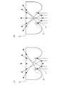
- FIGS. 1A and 1B are diagrams for explaining the diffusion performance of the radiation angle expanding element.
- FIG. 1A is a partial cross-sectional view schematically showing a radiation angle expanding element 1 having an ideal microlens shape.
- FIG. 1B is a partial cross-sectional view schematically showing an actual radiation angle enlarging element 2.
- the end portion 6 of the microlens 5 in the actual radiation angle expansion element 2 is dull than the end portion 4 of the microlens 3 in the ideal radiation angle expansion element 1.
- the actual curvature of the end 6 of the microlens 5 tends to be smaller than the curvature of the end 4 of the ideal microlens 3.
- the blunting of the microlens edge is largely due to manufacturing factors.
- As a method of manufacturing a radiation angle enlarging element it is known in the industry to transfer-mold from a mother mold (master mold) to manufacture a product (mold).
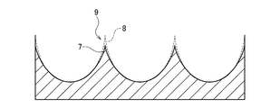
- Fig. 2 is a diagram comparing the ideal master mold with the actual master mold.
- a broken line schematically shows a partial cross section of an ideal (that is, designed) master mold 8
- a solid line schematically shows a partial cross section of an actually manufactured master mold 7.
- the ridge line portion 9 of the master mold corresponding to the portion between the adjacent microlenses has a very sharp shape.
- the master mold As a method for producing the master mold, for example, there is a method of cutting the base material using a cutting tool or the like. However, such a very sharp shape is not easy to cut, and the ridge line portion of the actual master mold 7 is not easily cut. The shape of 9 tends to be dull than that of the ideal master mold 8. In other words, the actual curvature of the ridge portion of the master mold 7 tends to be smaller than the ideal curvature of the ridge portion of the master mold 8. The shape of the end portion of the microlens manufactured by using such a master mold 7 necessarily deviates from the designed shape, and there is a possibility that the desired diffusion performance cannot be realized.
- the present invention has been made in view of such circumstances, and an object thereof is to realize a desired diffusion performance in a radiation angle enlarging element having a plurality of two-dimensionally arranged microlens arrays.
- the radiation angle enlarging element includes a plurality of microlenses arranged two-dimensionally. A predetermined space is provided between adjacent microlenses.
- the predetermined interval may be an interval at which the closest length of adjacent microlenses is 100 nm or more.
- the microlenses may be rectangular lenses.
- the shape of the interval between the adjacent microlenses may be curved.
- a desired diffusion performance can be realized in a radiation angle expanding element in which a plurality of microlens arrays are two-dimensionally arranged.
- 1A and 1B are views for explaining the diffusion performance of the radiation angle expanding element. It is the figure which compared the ideal master mold and the actual master mold. It is a fragmentary sectional view showing the radiation angle expansion element concerning this embodiment typically. It is a fragmentary sectional view showing typically a master mold used for manufacturing a radiation angle expansion element concerning this embodiment. It is a top view for explaining one embodiment of a radiation angle expansion element. It is a top view for explaining another embodiment of a radiation angle expansion element. 7A to 7D are views for explaining a method of manufacturing the radiation angle expanding element. It is a top view for explaining the radiation angle expansion element concerning a 1st example. It is a figure which shows the radiation angle performance of the radiation angle expansion element which concerns on 1st Example.
- FIG. 3 is a partial sectional view schematically showing the radiation angle enlarging element 10 according to the present embodiment.
- the radiation angle enlarging element 10 is a microlens array in which a plurality of microlenses 12 are two-dimensionally arranged.
- the microlens 12 is a convex lens.
- the plurality of microlenses 12 may be, for example, square array or dense array.
- the outer shape of the microlens 12 may be circular in plan view or rectangular in plan view.
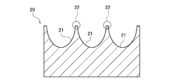
- FIG. 4 is a partial cross-sectional view schematically showing the master mold 20 used for manufacturing the radiation angle enlarging element 10 according to the present embodiment.
- the master mold 20 includes a lens molding portion 21 for molding the microlens 12.
- a ridge line portion 22 is formed between the adjacent lens forming portions 21.
- the ridge line portion 22 corresponds to a portion between the adjacent microlenses 12 in the radiation angle expanding element 10.
- the radiation angle enlarging element 10 can be manufactured by filling such a master mold 20 with a transparent resin material and curing it.
- a predetermined space 14 is provided between the adjacent microlenses 12.
- the shape of the space 14 is flat.
- the curvature of the end portion of the microlens 12 molded using the master mold 20 can be set to a value as designed without reduction, and desired diffusion performance can be realized.
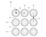
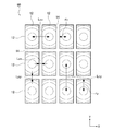
- FIG. 5 is a plan view for explaining an embodiment of the radiation angle expanding element.
- a plurality of microlenses 12 each having a circular outer shape in plan view are arranged in a square. As described above, the space 14 is provided between the adjacent microlenses 12.
- the optimum size of the space 14 between the adjacent microlenses 12 will be described.
- the present inventor has found that it is optimal to set the closest length Lp of the adjacent microlenses 12 to 100 nm or more.
- the interval 14 between the microlenses 12 so that the closest length Lp is 100 nm or more, it is possible to manufacture the radiation angle enlarging element 10 having the microlenses 12 in which the reduction in the curvature of the end portion is suppressed, and the desired diffusion is achieved. Performance can be realized.
- the closest length Lp is the minimum distance between the adjacent microlenses 12, and is a value obtained by subtracting the diameter (radius r ⁇ 2) of the microlenses 12 from the center-to-center distance Lc between the adjacent microlenses 12.
- the center-to-center distance Lc is the distance between the vertices of the adjacent microlenses 12.
- the apex of the microlens 12 is a point corresponding to the maximum height of the lens in the case of a convex lens, and a point corresponding to the minimum height of the lens in the case of a concave lens.
- FIG. 6 is a plan view for explaining another embodiment of the radiation angle expanding element.
- a plurality of microlenses 12 each having a rectangular outer shape in a plan view are arranged in a square.
- the microlens 12 is a convex lens.
- the space 14 is provided between the adjacent microlenses 12.
- the spacing 14 in the X direction and the spacing 14 in the Y direction may be different from each other. That is, the closest length Lpx in the X direction and the closest length Lpy in the Y direction may be different from each other.
- the closest length Lpx in the X direction is a value obtained by subtracting the diameter of the microlens 12 in the X direction (radius rx ⁇ 2 in the X direction) from the center-to-center distance Lcx of the microlenses 12 adjacent in the X direction.
- the closest length Lpy in the Y direction is a value obtained by subtracting the diameter of the microlens 12 in the Y direction (radius ry ⁇ 2 in the Y direction) from the center-to-center distance Lcy of the microlenses 12 adjacent in the Y direction.
- the closest length can be measured by observing the cross-section SEM after molding the radiation angle enlarging element.
- the SEM may be any that can be observed at a magnification of 100,000 times or more, and can be observed using, for example, S-3700N manufactured by Hitachi High-Technologies Corporation.
- the sample is cut in a direction parallel to the array direction by passing through the apexes of at least one microlens 12 so that the closest length can be observed in section in advance.
- the cutting is preferably performed by using a slicer or FIB device.
- FIB Ethos NX5000 manufactured by Hitachi High-Technologies Corporation can be used.
- FIGS. 7A to 7D are views for explaining a method of manufacturing the radiation angle expanding element.
- the radiation angle enlarging element as a product may be transferred and molded directly from the master mold 20.
- the radiation angle enlarging element as a product may be transfer-molded after transfer-molding the mold a plurality of times from the master mold. By thus forming a product using the mold, the life of the master mold can be extended.
- FIG. 8 is a plan view for explaining the radiation angle expanding element 80 according to the first embodiment.
- a plurality of microlenses 12 whose outer shape is circular in plan view are arranged in a square.
- the shape of each microlens 12 is represented by the following mathematical expression (1).
- the values of each parameter in the mathematical expression (1) are shown in the table below.
- Transfer molding was performed from a master mold 20 as shown in FIG. 4 on a soda lime glass substrate using a resin material having a refractive index of 1.5.
- the material of the master mold 20 may be any of metal, glass and resin.
- the microlenses 12 are two-dimensionally arranged so that the closest length is 100 nm.
- FIG. 9 shows the radiation angle performance of the radiation angle expanding element 80 according to the first embodiment.
- light having a wavelength of 850 nm was transmitted through the radiation angle expanding element 80, and the radiation angle was measured.
- OP-TR/RF-GONIO-MIN manufactured by Ocean Photonics Co., Ltd. was used.
- a plurality of microlenses are arranged in a square.
- the microlenses are two-dimensionally arranged so that the closest length is 1000 nm.
- a wide-angle (110°) diffusion performance was obtained.
- a comparative example will be explained. Also in the comparative example, a plurality of microlenses are arranged in a square. In the comparative example, no space was provided between the adjacent microlenses. That is, the closest contact length was set to 0 nm. Also in the comparative example, the radiation angle was measured in the same manner as in the first example, and the result was that the diffusion angle was 96°, and the diffusion performance was lower than in the first and second examples. From the comparison between the comparative example and the first and second examples, the effectiveness of setting the closest length of the adjacent microlenses to 100 nm or more was confirmed.
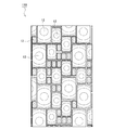
- FIG. 10 is a plan view for explaining the radiation angle enlarging element 100 according to the third embodiment.
- a plurality of microlenses 12 whose outer shape is circular in plan view are densely arranged.
- the microlenses 12 are two-dimensionally arranged so that the closest length is 100 nm or more.
- FIG. 11 is a plan view for explaining the radiation angle enlarging element 110 according to the fourth embodiment.
- a plurality of microlenses 12 each having a rectangular outer shape in plan view are randomly arranged.
- the microlenses 12 are two-dimensionally arranged so that the closest length is 100 nm or more.
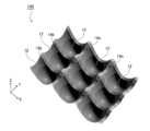
- FIG. 12 is a bird's-eye view for explaining a radiation angle enlarging element 120 according to still another embodiment of the present invention.
- the radiation angle enlarging element 120 is a microlens array in which a plurality of rectangular microlenses 12 are two-dimensionally arranged in a plan view.
- the microlens 12 is a convex lens.
- a space is provided between the adjacent microlenses 12.
- the shape of the interval between the adjacent microlenses 12 is a curved surface.
- the two-dimensional array of the microlenses 12 may be a rectangular array (an array in which the microlenses 12 are aligned along the X axis and the Y axis orthogonal to each other in a plan view) or a square array (a rectangular array and X
- the pitch between the lens vertices arranged along the axis and the pitch between the lens vertices arranged along the Y axis may be substantially equal).
- the radiation angle expanding element 120 in the cross-sectional view when the radiation angle expanding element 120 is cut along a plane parallel to the XZ plane, it corresponds to the interval between the microlenses 12 arranged along the X axis.
- the broken portion 14a is a line segment parallel to the X axis.
- the portion 14a corresponding to the interval between the microlenses 12 arranged along the X axis is a curved line having an upward convex shape. Has become.
- the radiation angle expanding element 120 in the cross-sectional view when the radiation angle expanding element 120 is cut in a plane parallel to the YZ plane, the space between the microlenses 12 arranged along the Y axis is shown.
- the corresponding portion 14b is a line segment parallel to the Y axis.
- a portion 14b corresponding to the interval between the microlenses 12 arranged along the Y axis is a curved line having an upward convex shape. Has become.
- FIG. 13 is a bird's-eye view for explaining a radiation angle enlarging element 130 according to still another embodiment of the present invention.
- the radiation angle enlarging element 130 is a microlens array in which a plurality of rectangular microlenses 12 are two-dimensionally arranged in a plan view.
- the microlens 12 is a concave lens.
- a space is provided between the adjacent microlenses 12.
- the shape of the interval between the adjacent microlenses 12 is a curved surface.
- the two-dimensional array of the microlenses 12 may be a rectangular array or a square array.
- the emission angle expansion element 130 in the cross-sectional view when the emission angle expansion element 130 is cut along a plane parallel to the XZ plane, it corresponds to the interval between the microlenses 12 arranged along the X axis.
- the broken portion 14a is a line segment parallel to the X axis.
- a portion 14a corresponding to the interval between the microlenses 12 arranged along the X axis is a downward convex curve. Has become.
- the emission angle expanding element 130 in the cross-sectional view when the emission angle expanding element 130 is cut in a plane parallel to the YZ plane, the space between the microlenses 12 arranged along the Y axis is shown.
- the corresponding portion 14b is a line segment parallel to the Y axis.
- a portion 14b corresponding to the interval between the microlenses 12 arranged along the Y axis is a downward convex curve. Has become.
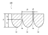
- FIG. 14 is a diagram for explaining the structure of the radiation angle expanding element 120 shown in FIG.
- the sizes of the microlenses 12 and the intervals 14 of the radiation angle expanding element 120 are defined as shown in FIG.
- “a” represents the thickness of the radiation angle expanding element 120
- “b” represents the base thickness
- “c” represents the Sag of the microlens 12
- “d” represents the distance between the microlenses 12.
- “P” represents the pitch of the microlenses 12.
- b a ⁇ c.
- a and b may include the thickness of the substrate.
- the thickness a of the radiation angle enlarging element 120 will be described. If the thickness a is too large, the thickness of the element becomes too large, which hinders downsizing, thinning, and height reduction of the element. On the other hand, if the thickness a is too small, the mechanical strength required for the element itself is insufficient, and it becomes difficult to obtain the required effect of enlarging the radiation angle when a force is applied. There is a risk of doing it.
- the thickness a may be in the range of 10 ⁇ m ⁇ a ⁇ 6000 ⁇ m, depending on the degree of the required radiation angle expansion effect, the refractive index of the material of the lens, and the like. Desirably, 50 ⁇ m ⁇ a ⁇ 3000 ⁇ m, More preferably, 100 ⁇ m ⁇ a ⁇ 1000 ⁇ m, More preferably, 250 ⁇ m ⁇ a ⁇ 750 ⁇ m.
- the pitch P of the microlenses 12 will be described. If the pitch P is too small, the microlens becomes too small, making it difficult to manufacture the master mold. On the other hand, if the pitch P is too large, the thickness (Sag:c) of the microlens becomes large in order to obtain the necessary radiation angle, and the moldability becomes poor.
- the value of the pitch P may be 3 ⁇ m ⁇ P ⁇ 500 ⁇ m, Desirably, 5 ⁇ m ⁇ P ⁇ 300 ⁇ m, More preferably, 10 ⁇ m ⁇ P ⁇ 200 ⁇ m, More preferably, it may be 20 ⁇ m ⁇ P ⁇ 150 ⁇ m.
- the relationship between the interval d and the pitch P will be described. If the interval d is too small with respect to the pitch P, it becomes difficult to obtain the effect of making the shape of the ridgeline portion 22 of the master mold the curvature as designed. On the contrary, if the distance d is too large with respect to the pitch P, the intensity of the transmitted light passing through the gap increases, and the uniformity of the emitted beam deteriorates.
- the value of the interval d may be 0.1 ⁇ m ⁇ d ⁇ 0.1 ⁇ P ⁇ m, depending on the degree of the required radiation angle expansion effect, the refractive index of the lens material, and the like.
- the value of the interval d may be 1/300 ⁇ c ⁇ m ⁇ d ⁇ 3/20 ⁇ c ⁇ m, depending on the degree of the required radiation angle expansion effect, the refractive index of the material of the lens, and the like. Desirably, 1/200 ⁇ c ⁇ m ⁇ d ⁇ 2/20 ⁇ c ⁇ m, More preferably, 1/100 ⁇ c ⁇ m ⁇ d ⁇ 1/20 ⁇ c ⁇ m, More preferably, 1/75 ⁇ c ⁇ m ⁇ d ⁇ 1/15 ⁇ c ⁇ m.
- the present invention can be used for a radiation angle expanding element for expanding the radiation angle of an incident beam.
Landscapes
- Physics & Mathematics (AREA)
- General Physics & Mathematics (AREA)
- Optics & Photonics (AREA)
- Optical Elements Other Than Lenses (AREA)
- Moulds For Moulding Plastics Or The Like (AREA)
Abstract
放射角度拡大素子10は、2次元配列された複数のマイクロレンズ12を備える。隣接するマイクロレンズ12間に所定の間隔14が設けられる。
Description
本発明は、入射ビームの放射角度を拡大する放射角度拡大素子に関する。
従来より、入射ビームの放射角度をより大きな放射角度に拡大する光学素子として、複数のマイクロレンズを2次元配列して成る放射角度拡大素子が知られている(例えば、特許文献1、2参照)。
放射角度拡大素子において、放射角を広くするためには、マイクロレンズのアスペクト比を高くする必要がある。特にマイクロレンズの端部は広角の放射角度成分に寄与しているため、マイクロレンズの端部の形状が設計形状から離れてしまうと拡散性能が低下する。
図1(A)および(B)は、放射角度拡大素子の拡散性能を説明するための図である。図1(A)は、理想的なマイクロレンズ形状を有する放射角度拡大素子1を模式的に示す部分断面図である。図1(B)は、実際の放射角度拡大素子2を模式的に示す部分断面図である。図1(A)および(B)に示すように、実際の放射角度拡大素子2におけるマイクロレンズ5の端部6は、理想的な放射角度拡大素子1のマイクロレンズ3の端部4よりも鈍る傾向がある。換言すると、実際のマイクロレンズ5における端部6の曲率は、理想的なマイクロレンズ3における端部4の曲率よりも小さくなりがちである。
このようなマイクロレンズ端部の鈍りは、製造上の要因によるところが大きい。放射角度拡大素子を製造する方法としては、例えば母型(マスターモールド)から転写成形して製品(モールド)を製造することが工業的に知られている。
図2は、理想的なマスターモールドと実際のマスターモールドを比較した図である。図2において、破線は理想的な(すなわち設計上の)マスターモールド8の部分断面を模式的に示し、実線は実際に作製されたマスターモールド7の部分断面を模式的に示す。図2に示すように、隣接するマイクロレンズ間の部分に対応するマスターモールドの稜線部分9は非常に尖った形状となる。
マスターモールドを作製する方法としては、例えばバイトなどを用いて母材を切削加工する方法があるが、このような非常に尖った形状は切削加工が容易ではなく、実際のマスターモールド7の稜線部分9の形状は、理想的なマスターモールド8のそれよりも鈍ったものとなりがちである。言い換えると、実際のマスターモールド7における稜線部分の曲率は、理想的なマスターモールド8の稜線部分の曲率よりも小さくなりがちである。このようなマスターモールド7を用いて製造されたマイクロレンズ端部の形状は必然的に設計形状から離れたものとなり、所望の拡散性能を実現できない可能性がある。
本発明はこうした状況に鑑みてなされたものであり、その目的は、複数のマイクロレンズアレイを2次元配置した放射角度拡大素子において、所望の拡散性能を実現することにある。
上記課題を解決するために、本発明のある態様の放射角度拡大素子は、2次元配列された複数のマイクロレンズを備える。隣接するマイクロレンズ間に所定の間隔が設けられる。
所定の間隔は、隣接するマイクロレンズの最近接長が100nm以上となる間隔であってもよい。マイクロレンズは、矩形レンズであってもよい。隣接するマイクロレンズ間の間隔の形状が曲面になっていてもよい。
なお、以上の構成要素の任意の組合せ、本発明の表現を方法、装置、システム、などの間で変換したものもまた、本発明の態様として有効である。
本発明によれば、複数のマイクロレンズアレイを2次元配置した放射角度拡大素子において、所望の拡散性能を実現できる。
以下、本発明の実施形態に係る放射角度拡大素子について説明する。各図面に示される同一または同等の構成要素、部材、処理には、同一の符号を付するものとし、適宜重複した説明は省略する。また、実施の形態は、発明を限定するものではなく例示であって、実施の形態に記述されるすべての特徴やその組み合わせは、必ずしも発明の本質的なものであるとは限らない。
図3は、本実施形態に係る放射角度拡大素子10を模式的に示す部分断面図である。放射角度拡大素子10は、複数のマイクロレンズ12が2次元配列されたマイクロレンズアレイである。本実施形態において、マイクロレンズ12は凸レンズである。複数のマイクロレンズ12は、例えば正方配列されてもよいし、稠密配列されてもよい。マイクロレンズ12の外形は、例えば平面視で円形であってもよいし、平面視で矩形であってもよい。
図4は、本実施形態に係る放射角度拡大素子10を製造するために用いられるマスターモールド20を模式的に示す部分断面図である。マスターモールド20は、マイクロレンズ12を成形するためのレンズ成形用部分21を備える。隣接するレンズ成形用部分21の間には稜線部分22が形成されている。稜線部分22は、放射角度拡大素子10における隣接するマイクロレンズ12間の部分に対応する。このようなマスターモールド20に透明な樹脂材料を充填して硬化させることにより、放射角度拡大素子10を製造することができる。
ここで、本実施形態に係る放射角度拡大素子10においては、図3に示すように隣接するマイクロレンズ12の間に所定の間隔14が設けられている。この間隔14の部分の形状は、平面となっている。このような間隔14を設けたことにより、マスターモールド20の稜線部分22をそれほど(すなわち図2で説明した従来技術ほど)尖った形状とする必要がなくなるので、稜線部分22の形状を設計通りの曲率に加工することが容易となる。その結果、マスターモールド20を用いて成形されるマイクロレンズ12の端部の曲率を低減なく設計通りの値とすることができ、所望の拡散性能を実現することができる。
図5は、放射角度拡大素子の一実施形態を説明するための平面図である。図5に示す放射角度拡大素子50においては、外形が平面視で円形の複数のマイクロレンズ12が正方配列されている。上述したように、隣接するマイクロレンズ12の間には間隔14が設けられている。
ここで、隣接するマイクロレンズ12間の間隔14の最適な大きさについて説明する。本発明者は、間隔14の最適値について鋭意検討した結果、隣接するマイクロレンズ12の最近接長Lpを100nm以上とすることが最適であることを見いだした。最近接長Lpが100nm以上となるようにマイクロレンズ12間に間隔14を設けることにより、端部の曲率の低減が抑制されたマイクロレンズ12を有する放射角度拡大素子10を製造でき、所望の拡散性能を実現することができる。なお、最近接長Lpとは、隣接するマイクロレンズ12間の最小距離であり、隣接するマイクロレンズ12の中心間距離Lcからマイクロレンズ12の直径(半径r×2)を引いた値となる。中心間距離Lcとは、隣接するマイクロレンズ12の頂点間の距離である。マイクロレンズ12の頂点とは、凸レンズの場合はレンズの最大高さに対応する点であり、凹レンズの場合はレンズの最小高さに対応する点である。
図6は、放射角度拡大素子の別の実施形態を説明するための平面図である。図6に示す放射角度拡大素子60においては、外形が平面視で矩形の複数のマイクロレンズ12が正方配列されている。本実施形態において、マイクロレンズ12は凸レンズである。上述したように、隣接するマイクロレンズ12の間には間隔14が設けられている。
図6に示す放射角度拡大素子60では、X方向における間隔14とY方向における間隔14が互いに異なっていてもよい。すなわち、X方向の最近接長LpxとY方向の最近接長Lpyとが互いに異なっていてもよい。X方向の最近接長Lpxは、X方向に隣接するマイクロレンズ12の中心間距離Lcxからマイクロレンズ12のX方向の直径(X方向の半径rx×2)を引いた値となる。Y方向の最近接長Lpyは、Y方向に隣接するマイクロレンズ12の中心間距離Lcyからマイクロレンズ12のY方向の直径(Y方向の半径ry×2)を引いた値となる。
最近接長は、放射角度拡大素子を成形後に断面SEM観察等を行うことによって計測することができる。SEMは10万倍以上の倍率で観察できるものであれよく、例えば株式会社日立ハイテクノロジーズのS-3700Nを使って観察することができる。事前に最近接長が断面観察できるようにサンプルを、少なくとも1個のマイクロレンズ12の頂点を通過し、配列方向に平行な方向で切断する。切断はスライサーやFIB装置を用いて行うのがよい。例えばFIBは株式会社日立ハイテクノロジーズのEthos NX5000を用いることができる。
図7(A)~(D)は、放射角度拡大素子の製造方法を説明するための図である。図7(A)に示すように、マスターモールド20から直接に製品としての放射角度拡大素子を転写成形してもよい。あるいは、図7(B)~(D)に示すように、マスターモールドから複数回モールドを転写成形してから、製品としての放射角度拡大素子を転写成形してもよい。このようにモールドを用いて製品を形成することにより、マスターモールドの寿命を延ばすことができる。
次に、放射角度拡大素子の実施例について説明する。図8は、第1実施例に係る放射角度拡大素子80を説明するための平面図である。第1実施例に係る放射角度拡大素子80では、外形が平面視で円形の複数のマイクロレンズ12が正方配列されている。個々のマイクロレンズ12の形状は、以下の数式(1)で表される。
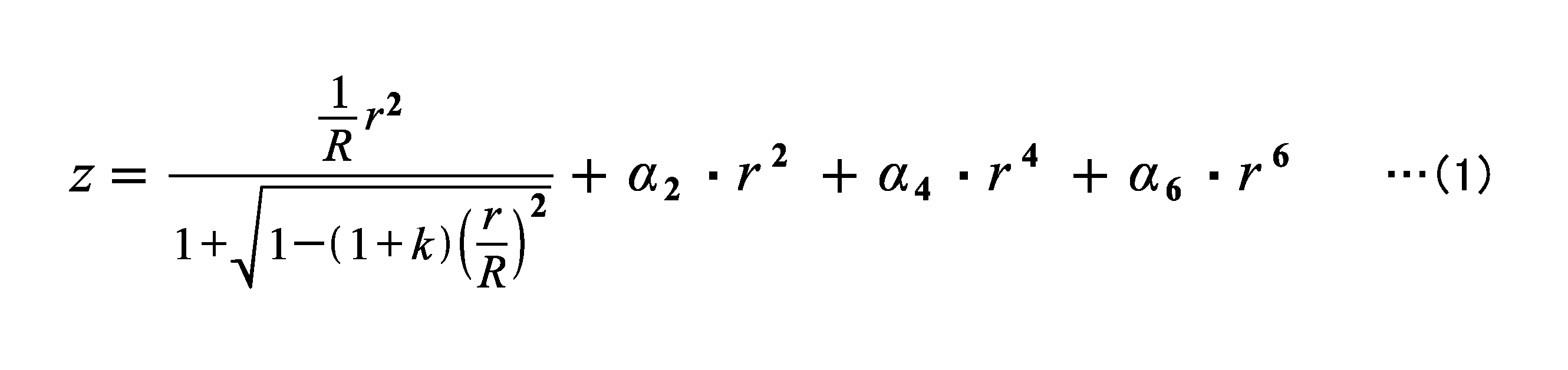
数式(1)における各パラメータの値を以下の表に示す。
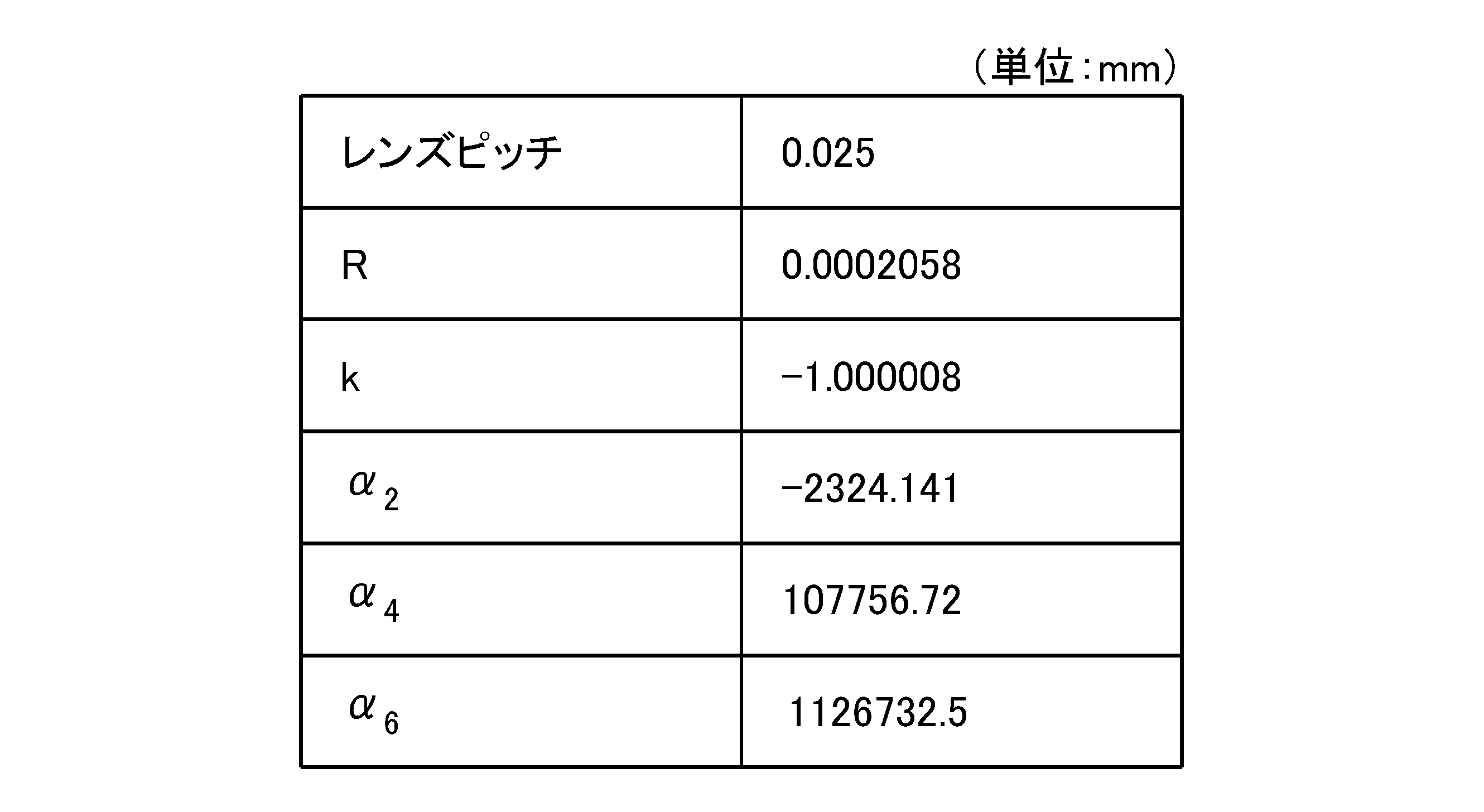
ソーダライムガラス基板に対して、屈折率1.5の樹脂材料を使用して図4に示すようなマスターモールド20から転写成形を行った。マスターモールド20の材質は、金属、ガラス、樹脂のいずれの材料であってもよい。第1実施例では、最近接長が100nmとなるようにマイクロレンズ12を2次元配列した。
図9は、第1実施例に係る放射角度拡大素子80の放射角度性能を示す。ここでは、放射角度拡大素子80に波長850nmの光を透過させ、放射角度を測定した。放射角度の測定は、オーシャンフォトニクス株式会社のOP-TR/RF-GONIO-MINを使用した。隣接するマイクロレンズ12の最近接長が100nmとなるように放射角度拡大素子80を形成したことにより、図9に示すように広角(110°)の拡散性能が得られた。
次に第2実施例について説明する。第2実施例においても、複数のマイクロレンズを正方配列した。第2実施例では、最近接長が1000nmとなるようにマイクロレンズを2次元配列した。第2実施例に関しても、第1実施例と同様に放射角度を測定した結果、広角(110°)の拡散性能が得られた。
次に比較例について説明する。比較例においても、複数のマイクロレンズを正方配列した。比較例では、隣接するマイクロレンズ間に間隔を設けなかった。すなわち、最近接長を0nmとした。比較例に関しても、第1実施例と同様に放射角度を測定した結果、拡散角は96°となり、第1および第2実施例と比較して拡散性能が低下した。比較例と第1および第2実施例の比較から、隣接するマイクロレンズの最近接長を100nm以上とすることの有効性が確認された。
図10は、第3実施例に係る放射角度拡大素子100を説明するための平面図である。第3実施例に係る放射角度拡大素子100では、外形が平面視で円形の複数のマイクロレンズ12が稠密配列されている。第3実施例でも、最近接長が100nm以上となるようにマイクロレンズ12が2次元配列される。
図11は、第4実施例に係る放射角度拡大素子110を説明するための平面図である。第4実施例に係る放射角度拡大素子110では、外形が平面視で矩形の複数のマイクロレンズ12がランダム配列されている。第4実施例でも、最近接長が100nm以上となるようにマイクロレンズ12を2次元配列される。
図12は、本発明のさらに別の実施形態に係る放射角度拡大素子120を説明するための鳥瞰図である。放射角度拡大素子120は、外形が平面視で矩形の複数のマイクロレンズ12が2次元配列されたマイクロレンズアレイである。本実施形態において、マイクロレンズ12は凸レンズである。図12に示すように、隣接するマイクロレンズ12間に間隔が設けられている。本実施形態に係る放射角度拡大素子120においては、隣接するマイクロレンズ12間の間隔の形状が曲面になっている。
マイクロレンズ12の2次元配列は、長方配列(平面視で直交するX軸およびY軸に沿ってマイクロレンズ12が整列する配列)であってもよいし、正方配列(長方配列でありX軸に沿って配列するレンズ頂点間のピッチと、Y軸に沿って配列するレンズ頂点間のピッチとが略等しい配列)であってもよい。
本実施形態に係る放射角度拡大素子120では、X-Z平面に平行な平面で放射角度拡大素子120を切断したときの断面図において、X軸に沿って配列したマイクロレンズ12間の間隔に対応した部分14aはX軸に平行な線分となっている。さらに、Y-Z平面に平行な平面で放射角度拡大素子120を切断したときの断面図において、X軸に沿って配列したマイクロレンズ12間の間隔に対応した部分14aは、上に凸の曲線となっている。
さらに本実施形態に係る放射角度拡大素子120では、Y-Z平面に平行な平面で放射角度拡大素子120を切断したときの断面図において、Y軸に沿って配列したマイクロレンズ12間の間隔に対応した部分14bはY軸に平行な線分となっている。さらに、X-Z平面に平行な平面で放射角度拡大素子120を切断したときの断面図において、Y軸に沿って配列したマイクロレンズ12間の間隔に対応した部分14bは、上に凸の曲線となっている。
図13は、本発明のさらに別の実施形態に係る放射角度拡大素子130を説明するための鳥瞰図である。放射角度拡大素子130は、外形が平面視で矩形の複数のマイクロレンズ12が2次元配列されたマイクロレンズアレイである。本実施形態において、マイクロレンズ12は凹レンズである。図13に示すように、隣接するマイクロレンズ12間に間隔が設けられている。本実施形態に係る放射角度拡大素子130においても、隣接するマイクロレンズ12間の間隔の形状が曲面になっている。マイクロレンズ12の2次元配列は、長方配列であってもよいし、正方配列であってもよい。
本実施形態に係る放射角度拡大素子130では、X-Z平面に平行な平面で放射角度拡大素子130を切断したときの断面図において、X軸に沿って配列したマイクロレンズ12間の間隔に対応した部分14aはX軸に平行な線分となっている。さらに、Y-Z平面に平行な平面で放射角度拡大素子130を切断したときの断面図において、X軸に沿って配列したマイクロレンズ12間の間隔に対応した部分14aは、下に凸の曲線となっている。
さらに本実施形態に係る放射角度拡大素子130では、Y-Z平面に平行な平面で放射角度拡大素子130を切断したときの断面図において、Y軸に沿って配列したマイクロレンズ12間の間隔に対応した部分14bはY軸に平行な線分となっている。さらに、X-Z平面に平行な平面で放射角度拡大素子130を切断したときの断面図において、Y軸に沿って配列したマイクロレンズ12間の間隔に対応した部分14bは、下に凸の曲線となっている。
図14は、図12に示す放射角度拡大素子120の構造について説明するための図である。放射角度拡大素子120のマイクロレンズ12、間隔14のサイズを図14に示すように定義する。図14において、「a」は放射角度拡大素子120の厚みを表し、「b」は下地厚みを表し、「c」はマイクロレンズ12のSagを表し、「d」はマイクロレンズ12の間隔を表し、「P」はマイクロレンズ12のピッチを表す。ここで、b=a-cである。ただし、a、bは、基板の厚みを含んでもよい。
まず、放射角度拡大素子120の厚みaの望ましい範囲について説明する。厚みaが大きすぎると、素子の厚みが大きくなりすぎるため、素子の小型化、薄型化、低背化に支障がある。一方、厚みaが小さすぎると、素子自体に必要な機械的強度が不足し、力が加わった場合に変形して必要な放射角の拡大効果が得られにくくなったり、極端な場合は、破損してしまうおそれがある。
したがって、必要な放射角度拡大効果の程度、レンズの材料の屈折率等に依存するが、厚みaの範囲は、10μm<a<6000μm、であってよく、
望ましくは、50μm<a<3000μm、であってよく、
より望ましくは、100μm<a<1000μm、であってよく、
さらに望ましくは、250μm<a<750μm、であってよい。
望ましくは、50μm<a<3000μm、であってよく、
より望ましくは、100μm<a<1000μm、であってよく、
さらに望ましくは、250μm<a<750μm、であってよい。
次に、マイクロレンズ12のピッチPの望ましい範囲について説明する。ピッチPが小さすぎると、マイクロレンズが小さくなりすぎ、マスターモールドの作製が難しくなる。一方、ピッチPが大きすぎると、必要な放射角度を得るために、マイクロレンズの厚み(Sag:c)が大きくなり、成型性が悪くなる。
したがって、ピッチPの値は、3μm<P<500μm、であってよく、
望ましくは、5μm<P<300μm、であってよく、
より望ましくは、10μm<P<200μm、であってよく、
さらに望ましくは、20μm<P<150μm、であってよい。
望ましくは、5μm<P<300μm、であってよく、
より望ましくは、10μm<P<200μm、であってよく、
さらに望ましくは、20μm<P<150μm、であってよい。
次に、間隔dとピッチPの関係について説明する。ピッチPに対して、間隔dが小さすぎると、マスターモールドの稜線部分22の形状を設計通りの曲率にする効果が得られにくくなる。逆に、ピッチPに対して間隔dが大きすぎると、隙間部分を通過する透過光の強度が増し、出射ビームの均一性が悪くなる。
したがって、必要な放射角度拡大効果の程度、レンズの材料の屈折率等に依存するが、間隔dの値は、0.1μm<d<0.1×Pμm、であってよい。
次に、Sag(c)と間隔dの関係について説明する。Sag(c)に対して間隔dが小さすぎると、マスターモールドの稜線部分22の形状を設計通りの曲率にできにくくなる。逆に、Sag(c)に対して間隔dが大きすぎると、隙間部分を通過する透過光の強度が増し、出射ビームの均一性が悪くなる。
したがって、必要な放射角度拡大効果の程度、レンズの材料の屈折率等に依存するが、間隔dの値は、1/300×cμm<d<3/20×cμm、であってよく、
望ましくは、1/200×cμm<d<2/20×cμm、であってよく、
より望ましくは、1/100×cμm<d<1/20×cμm、であってよく、
さらに望ましくは、1/75×cμm<d<1/15×cμm、であってよい。
望ましくは、1/200×cμm<d<2/20×cμm、であってよく、
より望ましくは、1/100×cμm<d<1/20×cμm、であってよく、
さらに望ましくは、1/75×cμm<d<1/15×cμm、であってよい。
以上、本発明を実施の形態をもとに説明した。この実施の形態は例示であり、それらの各構成要素や各処理プロセスの組合せにいろいろな変形例が可能なこと、またそうした変形例も本発明の範囲にあることは当業者に理解されるところである。
本発明は、入射ビームの放射角度を拡大する放射角度拡大素子に利用できる。
10,50,60,80,100,110,120,130 放射角度拡大素子、 12 マイクロレンズ、 14 間隔、 20 マスターモールド。
Claims (8)
- 2次元配列された複数のマイクロレンズを備える放射角度拡大素子であって、
隣接する前記マイクロレンズ間に所定の間隔が設けられることを特徴とする放射角度拡大素子。 - 前記所定の間隔は、隣接する前記マイクロレンズの最近接長が100nm以上となる間隔であることを特徴とする請求項1に記載の放射角度拡大素子。
- 前記マイクロレンズは、矩形レンズであることを特徴とする請求項1または2に記載の放射角度拡大素子。
- 隣接する前記マイクロレンズ間の間隔の形状が曲面になっていることを特徴とする請求項1から3のいずれかに記載の放射角度拡大素子。
- 当該放射角度拡大素子の厚みをaとしたとき、10μm<a<6000μmであることを特徴とする請求項1から4のいずれかに記載の放射角度拡大素子。
- 前記マイクロレンズのピッチをPとしたとき、3μm<P<500μmであることを特徴とする請求項1から5のいずれかに記載の放射角度拡大素子。
- 前記マイクロレンズのピッチをPとし、前記所定の間隔をdとしたとき、0.1μm<d<0.1×Pμmであることを特徴とする請求項1から6のいずれかに記載の放射角度拡大素子。
- 前記マイクロレンズのSagをcとし、前記所定の間隔をdとしたとき、1/300×cμm<d<3/20×cμmであることを特徴とする請求項1から7のいずれかに記載の放射角度拡大素子。
Applications Claiming Priority (2)
| Application Number | Priority Date | Filing Date | Title |
|---|---|---|---|
| JP2019004486A JP2022049712A (ja) | 2019-01-15 | 2019-01-15 | 放射角度拡大素子 |
| JP2019-004486 | 2019-01-15 |
Publications (1)
| Publication Number | Publication Date |
|---|---|
| WO2020149209A1 true WO2020149209A1 (ja) | 2020-07-23 |
Family
ID=71613865
Family Applications (1)
| Application Number | Title | Priority Date | Filing Date |
|---|---|---|---|
| PCT/JP2020/000464 Ceased WO2020149209A1 (ja) | 2019-01-15 | 2020-01-09 | 放射角度拡大素子 |
Country Status (3)
| Country | Link |
|---|---|
| JP (1) | JP2022049712A (ja) |
| TW (1) | TW202028780A (ja) |
| WO (1) | WO2020149209A1 (ja) |
Citations (8)
| Publication number | Priority date | Publication date | Assignee | Title |
|---|---|---|---|---|
| JPH09197106A (ja) * | 1996-01-16 | 1997-07-31 | Toray Ind Inc | マイクロレンズアレイシートおよびそれを用いた液晶表示装置 |
| JPH10332904A (ja) * | 1997-06-03 | 1998-12-18 | Toppan Printing Co Ltd | レンチキュラーレンズシート及びその製造方法 |
| JP2002287256A (ja) * | 2001-03-27 | 2002-10-03 | Mitsubishi Rayon Co Ltd | 両面レンチキュラーレンズシート |
| JP2005141202A (ja) * | 2003-11-03 | 2005-06-02 | Arisawa Mfg Co Ltd | 透過型スクリーン |
| JP2006003522A (ja) * | 2004-06-16 | 2006-01-05 | Kuraray Co Ltd | マイクロレンズアレイおよびその製造方法 |
| JP2007328117A (ja) * | 2006-06-07 | 2007-12-20 | Sony Corp | レンチキュラーレンズシートおよびその製造方法、透過型スクリーンならびに背面投射型の画像表示装置 |
| JP2008083685A (ja) * | 2006-08-30 | 2008-04-10 | Hitachi Maxell Ltd | バックライト装置に用いられるマイクロレンズアレイシート及びマイクロレンズアレイシートを製造するためのロール版 |
| WO2018046903A1 (en) * | 2016-09-08 | 2018-03-15 | Bae Systems Plc | Diffusers for head up displays |
-
2019
- 2019-01-15 JP JP2019004486A patent/JP2022049712A/ja active Pending
-
2020
- 2020-01-09 WO PCT/JP2020/000464 patent/WO2020149209A1/ja not_active Ceased
- 2020-01-14 TW TW109101272A patent/TW202028780A/zh unknown
Patent Citations (8)
| Publication number | Priority date | Publication date | Assignee | Title |
|---|---|---|---|---|
| JPH09197106A (ja) * | 1996-01-16 | 1997-07-31 | Toray Ind Inc | マイクロレンズアレイシートおよびそれを用いた液晶表示装置 |
| JPH10332904A (ja) * | 1997-06-03 | 1998-12-18 | Toppan Printing Co Ltd | レンチキュラーレンズシート及びその製造方法 |
| JP2002287256A (ja) * | 2001-03-27 | 2002-10-03 | Mitsubishi Rayon Co Ltd | 両面レンチキュラーレンズシート |
| JP2005141202A (ja) * | 2003-11-03 | 2005-06-02 | Arisawa Mfg Co Ltd | 透過型スクリーン |
| JP2006003522A (ja) * | 2004-06-16 | 2006-01-05 | Kuraray Co Ltd | マイクロレンズアレイおよびその製造方法 |
| JP2007328117A (ja) * | 2006-06-07 | 2007-12-20 | Sony Corp | レンチキュラーレンズシートおよびその製造方法、透過型スクリーンならびに背面投射型の画像表示装置 |
| JP2008083685A (ja) * | 2006-08-30 | 2008-04-10 | Hitachi Maxell Ltd | バックライト装置に用いられるマイクロレンズアレイシート及びマイクロレンズアレイシートを製造するためのロール版 |
| WO2018046903A1 (en) * | 2016-09-08 | 2018-03-15 | Bae Systems Plc | Diffusers for head up displays |
Also Published As
| Publication number | Publication date |
|---|---|
| JP2022049712A (ja) | 2022-03-30 |
| TW202028780A (zh) | 2020-08-01 |
Similar Documents
| Publication | Publication Date | Title |
|---|---|---|
| US11378812B2 (en) | Diffuser plate and method for designing diffuser plate | |
| CN108139512B (zh) | 扩散板、显示装置、投影装置和照明装置 | |
| CN101533115B (zh) | 衍射光学元件、光学系统和光学装置 | |
| JP2019139163A (ja) | 拡散板、拡散板の設計方法、表示装置、投影装置及び照明装置 | |
| WO2018123466A1 (ja) | 光学体、拡散板、表示装置、投影装置及び照明装置 | |
| WO2018123465A1 (ja) | 反射型拡散板、表示装置、投影装置及び照明装置 | |
| KR20170129926A (ko) | 복합 확산판 | |
| US9557451B2 (en) | Diffusing plate having microlens array | |
| JP5027583B2 (ja) | バックライト装置に用いられるマイクロレンズアレイシート及びマイクロレンズアレイシートを製造するためのロール版 | |
| JP6543825B2 (ja) | マイクロレンズアレイ | |
| US11892154B2 (en) | Illumination device | |
| JP6265018B2 (ja) | 照明用光学シートおよびそれを用いた照明装置 | |
| JP2022049712A (ja) | 放射角度拡大素子 | |
| JP2009223191A (ja) | 光学素子 | |
| CN1138159C (zh) | 光学部件 | |
| JP2004101848A (ja) | マイクロレンズアレイ、マイクロレンズアレイを用いた光モジュール、及び光モジュールの位置決め方法 | |
| JP7483948B2 (ja) | 拡散板、発光デバイス及びセンサモジュール | |
| JP4934080B2 (ja) | 光制御体及び該光制御体の製造方法 | |
| CN101246235A (zh) | 光纤结构及其制造方法以及光纤照明装置 | |
| JPWO2019039526A1 (ja) | 光偏向デバイス | |
| KR20110001925A (ko) | 휘도강화 확산필름 | |
| JP5893916B2 (ja) | 照明装置及びそれが備える配光制御部材の作製方法 | |
| JP5757378B2 (ja) | 光学シート、光学部材、面光源装置、透過型表示装置および発光装置 | |
| TWI726083B (zh) | 光學元件、周期構造體、光學元件的製造方法及周期構造體的製造方法 | |
| JP4909287B2 (ja) | 光拡散モジュール |
Legal Events
| Date | Code | Title | Description |
|---|---|---|---|
| 121 | Ep: the epo has been informed by wipo that ep was designated in this application |
Ref document number: 20741713 Country of ref document: EP Kind code of ref document: A1 |
|
| NENP | Non-entry into the national phase |
Ref country code: DE |
|
| 122 | Ep: pct application non-entry in european phase |
Ref document number: 20741713 Country of ref document: EP Kind code of ref document: A1 |
|
| NENP | Non-entry into the national phase |
Ref country code: JP |