WO2020137146A1 - 半導体レーザ素子 - Google Patents
半導体レーザ素子 Download PDFInfo
- Publication number
- WO2020137146A1 WO2020137146A1 PCT/JP2019/042637 JP2019042637W WO2020137146A1 WO 2020137146 A1 WO2020137146 A1 WO 2020137146A1 JP 2019042637 W JP2019042637 W JP 2019042637W WO 2020137146 A1 WO2020137146 A1 WO 2020137146A1
- Authority
- WO
- WIPO (PCT)
- Prior art keywords
- semiconductor laser
- layer
- laser device
- semiconductor
- heater
- Prior art date
- Legal status (The legal status is an assumption and is not a legal conclusion. Google has not performed a legal analysis and makes no representation as to the accuracy of the status listed.)
- Ceased
Links
Images



















Classifications
-
- H—ELECTRICITY
- H01—ELECTRIC ELEMENTS
- H01S—DEVICES USING THE PROCESS OF LIGHT AMPLIFICATION BY STIMULATED EMISSION OF RADIATION [LASER] TO AMPLIFY OR GENERATE LIGHT; DEVICES USING STIMULATED EMISSION OF ELECTROMAGNETIC RADIATION IN WAVE RANGES OTHER THAN OPTICAL
- H01S5/00—Semiconductor lasers
- H01S5/02—Structural details or components not essential to laser action
- H01S5/0206—Substrates, e.g. growth, shape, material, removal or bonding
- H01S5/0207—Substrates having a special shape
-
- H—ELECTRICITY
- H01—ELECTRIC ELEMENTS
- H01S—DEVICES USING THE PROCESS OF LIGHT AMPLIFICATION BY STIMULATED EMISSION OF RADIATION [LASER] TO AMPLIFY OR GENERATE LIGHT; DEVICES USING STIMULATED EMISSION OF ELECTROMAGNETIC RADIATION IN WAVE RANGES OTHER THAN OPTICAL
- H01S5/00—Semiconductor lasers
- H01S5/20—Structure or shape of the semiconductor body to guide the optical wave ; Confining structures perpendicular to the optical axis, e.g. index or gain guiding, stripe geometry, broad area lasers, gain tailoring, transverse or lateral reflectors, special cladding structures, MQW barrier reflection layers
- H01S5/22—Structure or shape of the semiconductor body to guide the optical wave ; Confining structures perpendicular to the optical axis, e.g. index or gain guiding, stripe geometry, broad area lasers, gain tailoring, transverse or lateral reflectors, special cladding structures, MQW barrier reflection layers having a ridge or stripe structure
- H01S5/223—Buried stripe structure
- H01S5/2231—Buried stripe structure with inner confining structure only between the active layer and the upper electrode
-
- H—ELECTRICITY
- H01—ELECTRIC ELEMENTS
- H01S—DEVICES USING THE PROCESS OF LIGHT AMPLIFICATION BY STIMULATED EMISSION OF RADIATION [LASER] TO AMPLIFY OR GENERATE LIGHT; DEVICES USING STIMULATED EMISSION OF ELECTROMAGNETIC RADIATION IN WAVE RANGES OTHER THAN OPTICAL
- H01S5/00—Semiconductor lasers
- H01S5/02—Structural details or components not essential to laser action
- H01S5/024—Arrangements for thermal management
- H01S5/02453—Heating, e.g. the laser is heated for stabilisation against temperature fluctuations of the environment
-
- H—ELECTRICITY
- H01—ELECTRIC ELEMENTS
- H01S—DEVICES USING THE PROCESS OF LIGHT AMPLIFICATION BY STIMULATED EMISSION OF RADIATION [LASER] TO AMPLIFY OR GENERATE LIGHT; DEVICES USING STIMULATED EMISSION OF ELECTROMAGNETIC RADIATION IN WAVE RANGES OTHER THAN OPTICAL
- H01S5/00—Semiconductor lasers
- H01S5/04—Processes or apparatus for excitation, e.g. pumping, e.g. by electron beams
- H01S5/042—Electrical excitation ; Circuits therefor
- H01S5/0425—Electrodes, e.g. characterised by the structure
- H01S5/04256—Electrodes, e.g. characterised by the structure characterised by the configuration
-
- H—ELECTRICITY
- H01—ELECTRIC ELEMENTS
- H01S—DEVICES USING THE PROCESS OF LIGHT AMPLIFICATION BY STIMULATED EMISSION OF RADIATION [LASER] TO AMPLIFY OR GENERATE LIGHT; DEVICES USING STIMULATED EMISSION OF ELECTROMAGNETIC RADIATION IN WAVE RANGES OTHER THAN OPTICAL
- H01S5/00—Semiconductor lasers
- H01S5/10—Construction or shape of the optical resonator, e.g. extended or external cavity, coupled cavities, bent-guide, varying width, thickness or composition of the active region
- H01S5/16—Window-type lasers, i.e. with a region of non-absorbing material between the active region and the reflecting surface
- H01S5/162—Window-type lasers, i.e. with a region of non-absorbing material between the active region and the reflecting surface with window regions made by diffusion or disordening of the active layer
-
- H—ELECTRICITY
- H01—ELECTRIC ELEMENTS
- H01S—DEVICES USING THE PROCESS OF LIGHT AMPLIFICATION BY STIMULATED EMISSION OF RADIATION [LASER] TO AMPLIFY OR GENERATE LIGHT; DEVICES USING STIMULATED EMISSION OF ELECTROMAGNETIC RADIATION IN WAVE RANGES OTHER THAN OPTICAL
- H01S5/00—Semiconductor lasers
- H01S5/20—Structure or shape of the semiconductor body to guide the optical wave ; Confining structures perpendicular to the optical axis, e.g. index or gain guiding, stripe geometry, broad area lasers, gain tailoring, transverse or lateral reflectors, special cladding structures, MQW barrier reflection layers
- H01S5/22—Structure or shape of the semiconductor body to guide the optical wave ; Confining structures perpendicular to the optical axis, e.g. index or gain guiding, stripe geometry, broad area lasers, gain tailoring, transverse or lateral reflectors, special cladding structures, MQW barrier reflection layers having a ridge or stripe structure
- H01S5/227—Buried mesa structure ; Striped active layer
- H01S5/2275—Buried mesa structure ; Striped active layer mesa created by etching
-
- H—ELECTRICITY
- H01—ELECTRIC ELEMENTS
- H01S—DEVICES USING THE PROCESS OF LIGHT AMPLIFICATION BY STIMULATED EMISSION OF RADIATION [LASER] TO AMPLIFY OR GENERATE LIGHT; DEVICES USING STIMULATED EMISSION OF ELECTROMAGNETIC RADIATION IN WAVE RANGES OTHER THAN OPTICAL
- H01S5/00—Semiconductor lasers
- H01S5/30—Structure or shape of the active region; Materials used for the active region
- H01S5/34—Structure or shape of the active region; Materials used for the active region comprising quantum well or superlattice structures, e.g. single quantum well [SQW] lasers, multiple quantum well [MQW] lasers or graded index separate confinement heterostructure [GRINSCH] lasers
- H01S5/3403—Structure or shape of the active region; Materials used for the active region comprising quantum well or superlattice structures, e.g. single quantum well [SQW] lasers, multiple quantum well [MQW] lasers or graded index separate confinement heterostructure [GRINSCH] lasers having a strained layer structure in which the strain performs a special function, e.g. general strain effects, strain versus polarisation
- H01S5/3404—Structure or shape of the active region; Materials used for the active region comprising quantum well or superlattice structures, e.g. single quantum well [SQW] lasers, multiple quantum well [MQW] lasers or graded index separate confinement heterostructure [GRINSCH] lasers having a strained layer structure in which the strain performs a special function, e.g. general strain effects, strain versus polarisation influencing the polarisation
-
- H—ELECTRICITY
- H01—ELECTRIC ELEMENTS
- H01S—DEVICES USING THE PROCESS OF LIGHT AMPLIFICATION BY STIMULATED EMISSION OF RADIATION [LASER] TO AMPLIFY OR GENERATE LIGHT; DEVICES USING STIMULATED EMISSION OF ELECTROMAGNETIC RADIATION IN WAVE RANGES OTHER THAN OPTICAL
- H01S5/00—Semiconductor lasers
- H01S5/30—Structure or shape of the active region; Materials used for the active region
- H01S5/34—Structure or shape of the active region; Materials used for the active region comprising quantum well or superlattice structures, e.g. single quantum well [SQW] lasers, multiple quantum well [MQW] lasers or graded index separate confinement heterostructure [GRINSCH] lasers
- H01S5/343—Structure or shape of the active region; Materials used for the active region comprising quantum well or superlattice structures, e.g. single quantum well [SQW] lasers, multiple quantum well [MQW] lasers or graded index separate confinement heterostructure [GRINSCH] lasers in AIIIBV compounds, e.g. AlGaAs-laser, InP-based laser
- H01S5/3434—Structure or shape of the active region; Materials used for the active region comprising quantum well or superlattice structures, e.g. single quantum well [SQW] lasers, multiple quantum well [MQW] lasers or graded index separate confinement heterostructure [GRINSCH] lasers in AIIIBV compounds, e.g. AlGaAs-laser, InP-based laser with a well layer comprising at least both As and P as V-compounds
-
- G—PHYSICS
- G11—INFORMATION STORAGE
- G11B—INFORMATION STORAGE BASED ON RELATIVE MOVEMENT BETWEEN RECORD CARRIER AND TRANSDUCER
- G11B5/00—Recording by magnetisation or demagnetisation of a record carrier; Reproducing by magnetic means; Record carriers therefor
- G11B2005/0002—Special dispositions or recording techniques
- G11B2005/0005—Arrangements, methods or circuits
- G11B2005/0021—Thermally assisted recording using an auxiliary energy source for heating the recording layer locally to assist the magnetization reversal
-
- H—ELECTRICITY
- H01—ELECTRIC ELEMENTS
- H01S—DEVICES USING THE PROCESS OF LIGHT AMPLIFICATION BY STIMULATED EMISSION OF RADIATION [LASER] TO AMPLIFY OR GENERATE LIGHT; DEVICES USING STIMULATED EMISSION OF ELECTROMAGNETIC RADIATION IN WAVE RANGES OTHER THAN OPTICAL
- H01S2301/00—Functional characteristics
- H01S2301/14—Semiconductor lasers with special structural design for lasing in a specific polarisation mode
- H01S2301/145—TM polarisation
-
- H—ELECTRICITY
- H01—ELECTRIC ELEMENTS
- H01S—DEVICES USING THE PROCESS OF LIGHT AMPLIFICATION BY STIMULATED EMISSION OF RADIATION [LASER] TO AMPLIFY OR GENERATE LIGHT; DEVICES USING STIMULATED EMISSION OF ELECTROMAGNETIC RADIATION IN WAVE RANGES OTHER THAN OPTICAL
- H01S5/00—Semiconductor lasers
- H01S5/0014—Measuring characteristics or properties thereof
-
- H—ELECTRICITY
- H01—ELECTRIC ELEMENTS
- H01S—DEVICES USING THE PROCESS OF LIGHT AMPLIFICATION BY STIMULATED EMISSION OF RADIATION [LASER] TO AMPLIFY OR GENERATE LIGHT; DEVICES USING STIMULATED EMISSION OF ELECTROMAGNETIC RADIATION IN WAVE RANGES OTHER THAN OPTICAL
- H01S5/00—Semiconductor lasers
- H01S5/02—Structural details or components not essential to laser action
- H01S5/0201—Separation of the wafer into individual elements, e.g. by dicing, cleaving, etching or directly during growth
- H01S5/0202—Cleaving
-
- H—ELECTRICITY
- H01—ELECTRIC ELEMENTS
- H01S—DEVICES USING THE PROCESS OF LIGHT AMPLIFICATION BY STIMULATED EMISSION OF RADIATION [LASER] TO AMPLIFY OR GENERATE LIGHT; DEVICES USING STIMULATED EMISSION OF ELECTROMAGNETIC RADIATION IN WAVE RANGES OTHER THAN OPTICAL
- H01S5/00—Semiconductor lasers
- H01S5/02—Structural details or components not essential to laser action
- H01S5/026—Monolithically integrated components, e.g. waveguides, monitoring photo-detectors, drivers
- H01S5/0261—Non-optical elements, e.g. laser driver components, heaters
-
- H—ELECTRICITY
- H01—ELECTRIC ELEMENTS
- H01S—DEVICES USING THE PROCESS OF LIGHT AMPLIFICATION BY STIMULATED EMISSION OF RADIATION [LASER] TO AMPLIFY OR GENERATE LIGHT; DEVICES USING STIMULATED EMISSION OF ELECTROMAGNETIC RADIATION IN WAVE RANGES OTHER THAN OPTICAL
- H01S5/00—Semiconductor lasers
- H01S5/04—Processes or apparatus for excitation, e.g. pumping, e.g. by electron beams
- H01S5/042—Electrical excitation ; Circuits therefor
- H01S5/0425—Electrodes, e.g. characterised by the structure
- H01S5/04252—Electrodes, e.g. characterised by the structure characterised by the material
-
- H—ELECTRICITY
- H01—ELECTRIC ELEMENTS
- H01S—DEVICES USING THE PROCESS OF LIGHT AMPLIFICATION BY STIMULATED EMISSION OF RADIATION [LASER] TO AMPLIFY OR GENERATE LIGHT; DEVICES USING STIMULATED EMISSION OF ELECTROMAGNETIC RADIATION IN WAVE RANGES OTHER THAN OPTICAL
- H01S5/00—Semiconductor lasers
- H01S5/06—Arrangements for controlling the laser output parameters, e.g. by operating on the active medium
- H01S5/0607—Arrangements for controlling the laser output parameters, e.g. by operating on the active medium by varying physical parameters other than the potential of the electrodes, e.g. by an electric or magnetic field, mechanical deformation, pressure, light, temperature
- H01S5/0612—Arrangements for controlling the laser output parameters, e.g. by operating on the active medium by varying physical parameters other than the potential of the electrodes, e.g. by an electric or magnetic field, mechanical deformation, pressure, light, temperature controlled by temperature
-
- H—ELECTRICITY
- H01—ELECTRIC ELEMENTS
- H01S—DEVICES USING THE PROCESS OF LIGHT AMPLIFICATION BY STIMULATED EMISSION OF RADIATION [LASER] TO AMPLIFY OR GENERATE LIGHT; DEVICES USING STIMULATED EMISSION OF ELECTROMAGNETIC RADIATION IN WAVE RANGES OTHER THAN OPTICAL
- H01S5/00—Semiconductor lasers
- H01S5/20—Structure or shape of the semiconductor body to guide the optical wave ; Confining structures perpendicular to the optical axis, e.g. index or gain guiding, stripe geometry, broad area lasers, gain tailoring, transverse or lateral reflectors, special cladding structures, MQW barrier reflection layers
- H01S5/2004—Confining in the direction perpendicular to the layer structure
- H01S5/2018—Optical confinement, e.g. absorbing-, reflecting- or waveguide-layers
- H01S5/2031—Optical confinement, e.g. absorbing-, reflecting- or waveguide-layers characterized by special waveguide layers, e.g. asymmetric waveguide layers or defined bandgap discontinuities
-
- H—ELECTRICITY
- H01—ELECTRIC ELEMENTS
- H01S—DEVICES USING THE PROCESS OF LIGHT AMPLIFICATION BY STIMULATED EMISSION OF RADIATION [LASER] TO AMPLIFY OR GENERATE LIGHT; DEVICES USING STIMULATED EMISSION OF ELECTROMAGNETIC RADIATION IN WAVE RANGES OTHER THAN OPTICAL
- H01S5/00—Semiconductor lasers
- H01S5/20—Structure or shape of the semiconductor body to guide the optical wave ; Confining structures perpendicular to the optical axis, e.g. index or gain guiding, stripe geometry, broad area lasers, gain tailoring, transverse or lateral reflectors, special cladding structures, MQW barrier reflection layers
- H01S5/2054—Methods of obtaining the confinement
- H01S5/2081—Methods of obtaining the confinement using special etching techniques
- H01S5/209—Methods of obtaining the confinement using special etching techniques special etch stop layers
-
- H—ELECTRICITY
- H01—ELECTRIC ELEMENTS
- H01S—DEVICES USING THE PROCESS OF LIGHT AMPLIFICATION BY STIMULATED EMISSION OF RADIATION [LASER] TO AMPLIFY OR GENERATE LIGHT; DEVICES USING STIMULATED EMISSION OF ELECTROMAGNETIC RADIATION IN WAVE RANGES OTHER THAN OPTICAL
- H01S5/00—Semiconductor lasers
- H01S5/30—Structure or shape of the active region; Materials used for the active region
- H01S5/32—Structure or shape of the active region; Materials used for the active region comprising PN junctions, e.g. hetero- or double- heterostructures
- H01S5/3211—Structure or shape of the active region; Materials used for the active region comprising PN junctions, e.g. hetero- or double- heterostructures characterised by special cladding layers, e.g. details on band-discontinuities
- H01S5/3213—Structure or shape of the active region; Materials used for the active region comprising PN junctions, e.g. hetero- or double- heterostructures characterised by special cladding layers, e.g. details on band-discontinuities asymmetric clading layers
-
- H—ELECTRICITY
- H01—ELECTRIC ELEMENTS
- H01S—DEVICES USING THE PROCESS OF LIGHT AMPLIFICATION BY STIMULATED EMISSION OF RADIATION [LASER] TO AMPLIFY OR GENERATE LIGHT; DEVICES USING STIMULATED EMISSION OF ELECTROMAGNETIC RADIATION IN WAVE RANGES OTHER THAN OPTICAL
- H01S5/00—Semiconductor lasers
- H01S5/30—Structure or shape of the active region; Materials used for the active region
- H01S5/34—Structure or shape of the active region; Materials used for the active region comprising quantum well or superlattice structures, e.g. single quantum well [SQW] lasers, multiple quantum well [MQW] lasers or graded index separate confinement heterostructure [GRINSCH] lasers
- H01S5/343—Structure or shape of the active region; Materials used for the active region comprising quantum well or superlattice structures, e.g. single quantum well [SQW] lasers, multiple quantum well [MQW] lasers or graded index separate confinement heterostructure [GRINSCH] lasers in AIIIBV compounds, e.g. AlGaAs-laser, InP-based laser
- H01S5/34346—Structure or shape of the active region; Materials used for the active region comprising quantum well or superlattice structures, e.g. single quantum well [SQW] lasers, multiple quantum well [MQW] lasers or graded index separate confinement heterostructure [GRINSCH] lasers in AIIIBV compounds, e.g. AlGaAs-laser, InP-based laser characterised by the materials of the barrier layers
- H01S5/34366—Structure or shape of the active region; Materials used for the active region comprising quantum well or superlattice structures, e.g. single quantum well [SQW] lasers, multiple quantum well [MQW] lasers or graded index separate confinement heterostructure [GRINSCH] lasers in AIIIBV compounds, e.g. AlGaAs-laser, InP-based laser characterised by the materials of the barrier layers based on InGa(Al)AS
Definitions
- the present invention relates to a semiconductor laser device.
- the "heat-assisted recording” method is a method in which a laser diode (semiconductor laser element) is used as a heat source to temporarily weaken the force for holding a magnetic field to perform writing.
- the semiconductor laser device used in the “heat assisted recording” type recording apparatus is different from the conventional semiconductor laser device for optical pickup in that it has a small chip size and a high size. You need to get the output.
- Patent Document 2 discloses that a laser diode used in the thermally-assisted magnetic recording head disclosed in Patent Document 2 is preferably a chip that generates TM-mode polarized light.
- An object of the present invention is to provide a semiconductor laser device which can obtain TM mode oscillation, has high output, and is highly reliable.
- One embodiment of the present invention is a semiconductor laser device that oscillates in a TM mode, wherein a substrate, an n-type clad layer disposed on the front surface side of the substrate, and an n-type clad layer opposite to the substrate side. And a p-type clad layer disposed on the opposite side of the active layer from the n-type clad layer, the active layer for causing TM mode oscillation.
- a semiconductor laser device including a quantum well layer having tensile strain of, and the n-type cladding layer and the p-type cladding layer each being an AlGaAs layer.
- the quantum well layer has tensile strain for causing TM mode oscillation, so that the semiconductor laser element can be oscillated in TM mode.
- the n-type clad layer and the p-type clad layer are each made of an AlGaAs layer.
- AlGaAs has a lower resistance than InGaAlP that is generally used as a cladding layer of a semiconductor laser device that oscillates in the TM mode. Therefore, in this configuration, the series resistance can be reduced as compared with the semiconductor laser device in which the cladding layer is the InGaAlP layer. As a result, heat generation can be suppressed as compared with a semiconductor laser device in which the cladding layer is made of an InGaAlP layer, so that a semiconductor laser device with high output and high reliability can be obtained.
- an end face window structure that expands the band gap of the active layer is formed in the end face portion of the laser resonator.
- the active layer includes a plurality of the quantum well layers and a barrier layer sandwiched between the adjacent quantum well layers and having a compressive strain.
- the substrate is a GaAs substrate
- the quantum well layer is a GaAsP layer.
- the substrate is a GaAs substrate and the barrier layer is an InAlGaAs layer.
- the p-type cladding layer further includes a current confinement layer formed on a side opposite to the active layer and confining a current flowing through the active layer.
- the surface of the p-type cladding layer on the side opposite to the active layer when viewed in the cavity length direction has a flat portion parallel to the surface of the active layer and both sides of the flat portion. And an inclined surface that is inclined with respect to the surface of the active layer, a p-type GaAs cap layer is formed on the flat portion of the p-type cladding layer, and the current constriction is formed. The layer is formed so as to cover the inclined surface of the p-type cladding layer and the side surface of the p-type GaAs cap layer.
- the current constriction layer is a laminated film of an AlGaAs layer and a GaAs layer formed on the AlGaAs layer.
- a GaAs contact layer formed so as to cover the surface of the current constriction layer and the surface of the p-type GaAs cap layer, a p-side electrode formed on the GaAs contact layer, and It includes an N-side electrode formed on the back surface of the substrate.
- the semiconductor laminated structure has a pair of end faces that form a resonance surface of the laser resonator, a pair of side faces, and an upper edge that is continuous with the surface of the semiconductor laminated structure on the pair of side faces. And a first separation groove mark formed in the region.
- the first separation trench mark is formed over the entire length direction of the semiconductor laminated structure.
- the semiconductor laminated structure further has, on the pair of side surfaces, a second separation groove mark formed in a lower edge region continuous with the back surface of the semiconductor laminated structure.
- the second separation trench mark is formed in a longitudinal middle portion of the semiconductor laminated structure.
- a substrate an n-type clad layer disposed on the front surface side of the substrate, an active layer disposed on the opposite side of the n-type clad layer from the substrate, and the active layer.
- a semiconductor laminated structure having a p-type cladding layer arranged on the opposite side of the layer from the n-type cladding layer, and formed on a part of a surface of the semiconductor laminated structure opposite to the substrate side.
- a semiconductor laser device including a connected first heater electrode and a second heater electrode connected to the other end of the heater.
- the heater since the heater is provided, it is possible to control the temperature of the semiconductor laser element by driving and controlling the heater. Therefore, for example, it becomes possible to control the temperature of the semiconductor laser element so that the temperature of the semiconductor laser element becomes almost constant.
- the main part of the first heater electrode and the main part of the second heater electrode are respectively arranged on the opposite side of the heater from the p-side electrode for semiconductor laser.
- the main portion of the first heater electrode, the main portion of the second heater electrode, and the p-side electrode for semiconductor laser each have a portion thicker than the thickness of the heater.
- a portion thicker than the heater has a thickness of 5 times or more the thickness of the heater.
- the p-type cladding layer has a linear ridge portion, and the semiconductor laser p-side electrode is formed in a region including the ridge portion in a plan view. ..
- the heater is arranged in parallel with the ridge portion in a plan view.
- the heater extends linearly in a plan view.
- the heater extends in a meandering shape in plan view.
- the heater is composed of a laminated film of a Ti film formed on the insulating film and a Pt film laminated on the Ti film.
- a substrate an n-type clad layer disposed on the front surface side of the substrate, an active layer disposed on the opposite side of the n-type clad layer from the substrate, and the active layer.
- a semiconductor layered structure having a p-type clad layer disposed on the opposite side of the layer from the n-type clad layer, the main semiconductor laser having a surface opposite to the substrate side in the semiconductor layered structure.
- a main semiconductor laser region used as a and a heat source semiconductor laser region used as a heat source semiconductor laser is formed with a region separation groove, and in the main semiconductor laser region, the surface of the semiconductor laminated structure is formed.
- a first p-side electrode for the main semiconductor laser is formed, and a second p-side electrode for the heat source semiconductor laser is formed on the surface of the semiconductor laminated structure in the heat source semiconductor laser region.
- the present invention provides a semiconductor laser device.
- the main semiconductor laser and the semiconductor laser for heat source are provided, it is possible to control the temperature of the main semiconductor laser (semiconductor laser element) by driving and controlling the semiconductor laser for heat source. Therefore, for example, it becomes possible to control the temperature of the semiconductor laser device so that the temperature of the main semiconductor laser becomes almost constant.
- the area separation groove reaches the substrate.
- an n-side electrode for the main semiconductor laser and the heat source semiconductor laser is formed on the back surface of the semiconductor laminated structure opposite to the front surface.
- the p-type cladding layer in the main semiconductor laser region, has a linear first ridge portion, and in the heat source semiconductor laser region, the p-type cladding layer is It has a linear second ridge portion.
- the second ridge portion is composed of a plurality of rectangular ridge portions linearly arranged at intervals in a plan view.
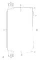
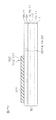
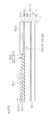
- FIG. 1 is a perspective view showing the outer appearance of a semiconductor laser device according to the first embodiment of the present invention.
- FIG. 2 is a front view of the semiconductor laser device of FIG.
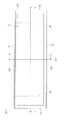
- FIG. 3 is a plan view of the semiconductor laser device of FIG.
- FIG. 4 is a bottom view of the semiconductor laser device of FIG.
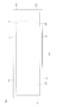
- FIG. 5 is a schematic sectional view taken along the line VV of FIG.
- FIG. 6 is a schematic sectional view taken along the line V1-VI of FIG.
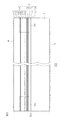
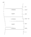
- FIG. 7 is a schematic sectional view for explaining the configuration of the active layer of the semiconductor laser device of FIG.
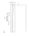
- FIG. 8 is a schematic sectional view showing a manufacturing process of the semiconductor laser device.
- FIG. 9 is a schematic sectional view showing a manufacturing process of the semiconductor laser device.
- FIG. 9 is a schematic sectional view showing a manufacturing process of the semiconductor laser device.
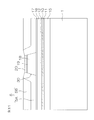
- FIG. 10 is a schematic sectional view showing a manufacturing process of the semiconductor laser device.
- FIG. 11 is a schematic sectional view showing a manufacturing process of a semiconductor laser device.
- FIG. 12 is a schematic sectional view showing a manufacturing process of a semiconductor laser device.
- FIG. 13 is a plan view showing the manufacturing process of the semiconductor laser device.
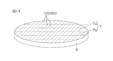
- FIG. 14 is a schematic plan view showing a part of a wafer in which a plurality of individual elements are formed.
- FIG. 15 is a schematic plan view showing the first separation groove formed on the surface of the semiconductor laminated structure.
- 16A is a partially enlarged cross-sectional view taken along the line XVI-XVI of FIG.
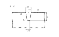
- FIG. 16B is a sectional view showing a modified example of the sectional shape of the first separation groove.
- FIG. 16A is a partially enlarged cross-sectional view taken along the line XVI-XVI of FIG.
- FIG. 16B is a sectional view showing a modified example of the section
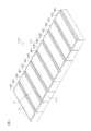
- FIG. 17 is a schematic perspective view showing a bar-shaped body obtained by primary cleavage.
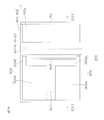
- FIG. 18 is a schematic bottom view showing the second separation groove formed on the back surface of the bar-shaped body.
- FIG. 19 is a schematic perspective view showing an individual element obtained from a bar-shaped body by secondary cleavage.
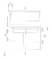
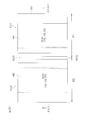
- FIG. 20A is a graph showing applied current-optical output characteristics of the first embodiment.
- FIG. 20B is a graph showing applied current-light output characteristics of the comparative example.
- 21 is a schematic sectional view of a semiconductor laser device according to a second embodiment of the present invention, which is a sectional view corresponding to a section of FIG.
- FIG. 22 is a schematic sectional view of the semiconductor laser device according to the third embodiment of the present invention, which is a sectional view corresponding to the section plane of FIG.
- FIG. 23 is a schematic perspective view showing the external appearance of the semiconductor laser device according to the fourth embodiment of the present invention.
- FIG. 24 is a schematic plan view of the semiconductor laser device of FIG.
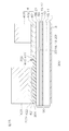
- FIG. 25 is a schematic sectional view taken along the line XXV-XXV in FIG.
- FIG. 26A is a schematic plan view showing an example of a manufacturing process of the semiconductor laser device of FIG. 23.
- FIG. 26B is a schematic plan view showing a step subsequent to FIG. 26A.
- FIG. 26C is a schematic plan view showing a step subsequent to FIG. 26B.
- FIG. 26D is a schematic plan view showing a step subsequent to FIG. 26C.
- FIG. 26E is a schematic plan view showing a step subsequent to FIG. 26D.
- FIG. 26F is a schematic plan view showing a step subsequent to FIG. 26E.
- FIG. 27A is a schematic sectional view showing an example of a manufacturing process of the semiconductor laser device of FIG. 23.
- FIG. 27B is a schematic sectional view showing a step subsequent to FIG. 27A.
- FIG. 27C is a schematic sectional view showing a step subsequent to FIG. 27B.
- FIG. 27D is a schematic sectional view showing a step subsequent to FIG. 27C.
- FIG. 27E is a schematic sectional view showing a step subsequent to FIG. 27D.
- FIG. 27F is a schematic sectional view showing a step subsequent to FIG. 27E.
- FIG. 28 is a schematic plan view showing another example of the heater.
- FIG. 29 is a schematic perspective view showing the external appearance of the semiconductor laser device according to the fifth embodiment of the present invention.
- FIG. 30 is a schematic plan view of the semiconductor laser device of FIG.
- FIG. 31 is a schematic sectional view taken along the line XXXI-XXXI in FIG.
- FIG. 32 is a schematic plan view showing another example of the ridge formed in the semiconductor laser region for heat source.
- FIG. 1 is a perspective view showing the outer appearance of a semiconductor laser device according to the first embodiment of the present invention.
- FIG. 2 is a front view of the semiconductor laser device of FIG.
- FIG. 3 is a plan view of the semiconductor laser device of FIG.
- FIG. 4 is a bottom view of the semiconductor laser device of FIG.
- FIG. 5 is a schematic sectional view taken along the line VV of FIG.
- FIG. 6 is a schematic sectional view taken along the line V1-VI of FIG.
- This semiconductor laser device 60 includes a substrate 1, a semiconductor laminated structure (semiconductor laminated structure in a narrow sense) 2 formed by crystal growth on the substrate 1, and a back surface of the substrate 1 (a surface opposite to the semiconductor laminated structure 2).
- the Fabry-Perot type is provided with an n-side electrode 3 formed in contact with the p-side electrode 4 formed in contact with the surface of the semiconductor laminated structure 2.
- the substrate 1 is composed of a GaAs single crystal substrate in this embodiment.
- the plane orientation of the surface of the GaAs substrate 1 is the (100) plane.
- Each layer forming the semiconductor laminated structure 2 is epitaxially grown on the substrate 1.
- Epitaxial growth refers to crystal growth with the lattice continuity from the underlayer being maintained. The lattice mismatch with the underlayer is absorbed by the strain of the lattice of the crystal grown layer, and the continuity of the lattice at the interface with the underlayer is maintained.
- the semiconductor laminated structure 2 includes an active layer 10, an n-side guide layer 11, a p-side guide layer 12, an n-type semiconductor layer 13, and a p-type semiconductor layer 14.
- the n-type semiconductor layer 13 is arranged on the substrate 1 side with respect to the active layer 10, and the p-type semiconductor layer 14 is arranged on the p-side electrode 4 side with respect to the active layer 10.
- the n-side guide layer 11 is arranged between the n-type semiconductor layer 13 and the active layer 10, and the p-side guide layer 12 is arranged between the active layer 10 and the p-type semiconductor layer 14. In this way, a double heterojunction is formed. Electrons are injected into the active layer 10 from the n-type semiconductor layer 13 via the n-side guide layer 11, and holes are injected from the p-type semiconductor layer 14 via the p-side guide layer 12. Light is generated by recombination of these in the active layer 10.
- the n-type semiconductor layer 13 is formed by forming an n-type AlGaAs cladding layer 15 (for example, 20000 ⁇ to 35000 ⁇ thickness) on the substrate 1.
- the n-type AlGaAs cladding layer 15 is made of, for example, an Al x Ga.sub. (1-x) As (0 ⁇ x ⁇ 1) layer.
- the p-type semiconductor layer 14 includes the first p-type AlGaAs cladding layer 16 (for example, 1000 ⁇ to 2000 ⁇ thickness), the p-type InGaP etching stop layer 17 (for example, 50 ⁇ to 300 ⁇ thickness), and the second p-type on the p-side guide layer 12.
- AlGaAs cladding layer 18 for example, 8000 ⁇ to 12000 ⁇ thickness
- p-type InGaP etching stop layer 19 for example, 50 ⁇ to 300 ⁇ thickness
- p-type GaAs cap layer 20 for example, 1000 ⁇ to 3000 ⁇ thickness
- p-type GaAs contact layer 21 for example, 30,000 ⁇ ). (Up to 60,000 ⁇ thickness) is laminated.
- the first p-type AlGaAs cladding layer 16 is made of, for example, an Al x Ga.sub. (1-x) As (0 ⁇ x ⁇ 1) layer.
- the second p-type AlGaAs cladding layer 18 is, for example, a p-type Al x Ga (1-x) As (0 ⁇ x ⁇ 1) layer (for example, 8000 ⁇ to 12000 ⁇ thickness) layer formed on the p-type InGaP etching stop layer 17. Consists of.
- the p-type GaAs contact layer 21 is a low resistance layer for taking ohmic contact with the p-side electrode 4.
- the p-type GaAs contact layer 21 is formed as a p-type semiconductor layer by doping GaAs with Be as a p-type dopant, for example.
- the n-type cladding layer 15 and the first and second p-type cladding layers 16 and 18 have a carrier confinement effect of confining carriers (electrons and holes) in the active layer 10 and light from the active layer 10 between them. The effect of confining light is generated.
- the n-type AlGaAs cladding layer 15 is formed as an n-type semiconductor layer by doping AlGaAs with, for example, Si as an n-type dopant.
- the first and second p-type AlGaAs cladding layers 16 and 18 are made into p-type semiconductor layers by doping AlGaAs with Be as a p-type dopant, for example.
- the n-type AlGaAs cladding layer 15 has a wider bandgap than the n-side guide layer 11, and the first and second p-type AlGaAs cladding layers 16 and 18 have a wider bandgap than the p-side guide layer 12. Thereby, good carrier confinement and light confinement can be performed, and a highly efficient semiconductor laser device can be realized.
- an end face window structure 35 for expanding the band gap of the active layer 10 by diffusing impurities such as zinc into the end face portion of the laser resonator.
- the n-side guide layer 11 is made of an AlGaAs layer (for example, 200 ⁇ to 500 ⁇ thick), and is formed by being laminated on the n-type semiconductor layer 13.
- the p-side guide layer 12 is made of AlGaAs (for example, 200 ⁇ to 500 ⁇ thickness) and is formed by being laminated on the active layer 10.
- the n-side guide layer 11 and the p-side guide layer 12 are each made of, for example, an Al x Ga.sub. (1-x) As (0 ⁇ x ⁇ 1) layer.
- the n-side AlGaAs guide layer 11 and the p-side AlGaAs guide layer 12 are semiconductor layers that produce an optical confinement effect in the active layer 10, and form a carrier confinement structure in the active layer 10 together with the clad layers 15, 16 and 18. doing. As a result, the efficiency of recombination of electrons and holes in the active layer 10 is improved.
- the active layer 10 has a multiple-quantum well (MQW) structure, and is a layer for amplifying the generated light by generating light by recombination of electrons and holes. is there.
- MQW multiple-quantum well
- the active layer 10 includes a quantum well layer 221 made of an undoped GaAsP layer (for example, a thickness of 60 ⁇ to 120 ⁇ ) and a barrier layer 222 made of an undoped InAlGaAs layer. It has a multiple quantum well structure constituted by alternately stacking and repeatedly for a plurality of cycles.
- the active layer 10 is composed of (Al x Ga.sub. (1-x) ) (1-y) In y As barrier layer 222 (for example, 20 ⁇ to 90 ⁇ thickness) and GaAs (1-x) P x quantum well.
- the layer 221 (for example, 60 ⁇ to 120 ⁇ thickness), the (Al x Ga (1-x) ) (1-y) In y As barrier layer 222 (for example, 40 ⁇ to 100 ⁇ thickness), and the GaAs (1-x) P x quantum.
- Well layer 221 (for example, 60 ⁇ to 120 ⁇ thickness) and (Al x Ga (1-x) ) (1-y) In y As barrier layer 222 (for example, 20 ⁇ to 90 ⁇ thickness) are laminated in this order from the bottom. Composed of a membrane.
- the semiconductor laser device 60 can oscillate in the TM mode.
- the semiconductor laser element oscillates in the TM mode when the polarization ratio of the output light of the semiconductor laser element is 5 [dB] or more.
- the electric field is biased in the direction perpendicular to the heterojunction plane.
- the compressive stress is applied to the barrier layer 222 formed of the (Al x Ga.sub. (1-x) ) (1-y) In y As layer. Is occurring.
- tensile strain is generated in the quantum well layer 221
- compressive strain is generated in the barrier layer 222, so that the strain of the entire active layer 10 is relaxed. This suppresses crystal deterioration during energization, so that the reliability of the semiconductor laser device can be improved.
- the second p-type cladding layer 18, the p-type etching stop layer 19, and the p-type cap layer 20 in the p-type semiconductor layer 14 are partially removed, so that a linear ridge is formed.
- Forming 30 More specifically, the second p-type cladding layer 18, the p-type etching stop layer 19 and a part of the p-type cap layer 20 are removed by etching to form a ridge 30 having a substantially trapezoidal cross section (mesa shape). ing. Therefore, the second p-type cladding layer 18 includes a flat portion in the width center portion parallel to the surface of the active layer 10, and inclined surfaces formed on both sides of the flat portion and inclined downward toward the outside. ..
- a current confinement layer (embedded layer) 5 (for example, 8000 ⁇ to 15000 ⁇ thickness) is formed on the side surface of the ridge 30. More specifically, the side surface of the p-type cap layer 20, the side surface of the p-type etching stop layer 19, the exposed surface of the second p-type cladding layer 18, and the exposed surface of the p-type etching stop layer 17 are the current confinement layer. Covered by 5. The exposed surfaces of the current constriction layer 5 and the p-type cap layer 20 are covered with the contact layer 21.
- the current confinement layer 5 is composed of a lower layer 5A formed on the p-type etching stop layer 17 and an upper layer 5B formed on the lower layer.
- the lower layer 5A is, for example, an Al x Ga.sub. (1-x) As layer (for example, 5000 ⁇ to 10000 ⁇ thickness)
- the upper layer 5B is, for example, a GaAs layer (for example, 1500 ⁇ to 7000 ⁇ thickness). Since the boundary between the upper layer 5B of the current constriction layer 5 and the contact layer 21 is not clear, it is indicated by a chain line.
- the semiconductor laminated structure 2 has a pair of end faces (cleavage planes) 31 and 32 which are mirror surfaces formed by cleavage planes at both ends in the longitudinal direction of the ridge 30.
- the pair of end faces 31 and 32 are parallel to each other.
- the n-side guide layer 11, the active layer 10, and the p-side guide layer 12 form a Fabry-Perot resonator having the pair of end faces 31 and 32 as resonator end faces. That is, the light generated in the active layer 10 is amplified by stimulated emission while reciprocating between the cavity end faces 31 and 32. Then, a part of the amplified light is taken out of the element as laser light from the resonator end faces 31 and 32.
- the semiconductor laminated structure 50 (broadly defined semiconductor laminated structure) including the substrate 1, the semiconductor laminated structure 2, and the current constriction layer 5 has a pair of side surfaces 33 and 34 parallel to the ridge 30.
- the semiconductor laminated structure 50 is cleaved from the wafer (precisely, a bar-shaped body 110 (see FIG. 17) described later) serving as the original substrate into the upper edge region on the front surface side.
- the first separation groove traces 8 (first divided guide grooves) 80 (see FIG. 15 and FIG. 16A) formed to achieve the above are formed over the entire length direction.
- the upper edge region is a region continuous with the surface of the semiconductor laminated structure 50 (the surface on the p-type semiconductor layer 14 side).
- the length direction is the longitudinal direction of the ridge 30 (resonator length direction).
- the semiconductor laminated structure 50 is an example of the semiconductor laminated structure of the present invention.
- the wafer as the original substrate (precisely, a bar-shaped member 110 (see FIG. 17) described later) from the semiconductor laminated structure
- a second separation groove mark 9 (see FIG. 18), which is formed by cleaving and dividing 50, is formed over the entire length direction.
- the lower edge area is an area continuous with the back surface of the substrate 1.
- the n-side electrode 3 is made of, for example, AuGeNi/Ti/Au alloy, and is ohmic-bonded to the substrate 1 so that the AuGeNi side is arranged on the substrate 1 side.
- the p-side electrode 4 includes a first electrode film formed on the p-type contact layer 21 and a second electrode film (formed on the first electrode film.
- the first electrode film is, for example, Ti/Au. It is made of an alloy and is ohmic-bonded to the p-type contact layer 21 so that its Ti side is arranged on the p-type contact layer 21 side.
- the second electrode film is made of, for example, Au plating.
- an end face window structure 35 for enlarging the band gap of the active layer 10 is formed in the end face portion of the resonator.
- the end face window structure 35 is formed, for example, by diffusing zinc (Zn) in the end face portion of the resonator.
- a reflection film for protecting the resonator end surface is formed on the resonator end surface.
- the n-side electrode 3 and the p-side electrode 4 are connected to a power source, and electrons and holes are injected from the n-type semiconductor layer 13 and the p-type semiconductor layer 14 into the active layer 10 to form the active layer. It is possible to cause the recombination of electrons and holes within 10 to generate, for example, light having an oscillation wavelength of 780 nm or more and 830 nm or less. This light reciprocates between the cavity end faces 31 and 32 along the guide layers 11 and 12, and is amplified by stimulated emission. Then, a larger amount of laser output is taken out from the resonator end face 31 which is the laser emission end face.
- FIGS. 8 to 13 are schematic sectional views showing a method for manufacturing the semiconductor laser device 60 shown in FIGS. 1 to 6.
- FIGS. 8 and 10 to 12 are schematic sectional views of the central portion corresponding to FIG. 6, and
- FIG. 9 is a schematic sectional view of the vicinity of the end portion.
- FIG. 13 is a plan view.
- an n-type AlGaAs cladding layer 15, an n-side AlGaAs guide layer 11, and an active layer 10 are formed on a GaAs substrate 1 by metalorganic chemical vapor deposition (MOCVD) by MOCVD (Metal Organic Chemical Vapor Deposition).
- MOCVD metalorganic chemical vapor deposition
- MOCVD Metal Organic Chemical Vapor Deposition
- P-side AlGaAs guide layer 12, first p-type AlGaAs cladding layer 16, p-type InGaP etching stop layer 17, second p-type AlGaAs cladding layer 18, p-type InGaP etching stop layer 19 and p-type GaAs cap layer 20 are grown in this order. ..
- the active layer 10 is formed by alternately and repeatedly growing a barrier layer 222 made of an InAlGaAs layer and a quantum well layer 221 made of a GaAsP layer for a plurality of cycles.
- ZnO (zinc oxide) 71 is patterned on the p-type GaAs cap layer 20 in a region corresponding to the vicinity of the end face of the semiconductor laser device 60. Then, for example, by performing an annealing treatment, Zn is diffused in a region corresponding to the vicinity of the end face of the semiconductor laser device 60. As a result, the end face window structure 35 is formed in a region corresponding to the vicinity of the end face of the semiconductor laser device 60.
- the ZnO layer 71 is removed. Then, as shown in FIG. 10, the p-type cap layer 20, the p-type etching stop layer 19 and a part of the second p-type cladding layer 18 are removed by etching using the striped SiO 2 insulating film as a mask layer 72. .. Then, the ridge stripe 30 having the mask layer 72 laminated on the top surface is formed.
- the lower layer 5A and the upper layer 5B of the current confinement layer 5 are sequentially formed on the surface, and then the mask layer 72 is removed. Then, as shown in FIG. 12, a p-type contact layer 21 is grown on the surface. Finally, the p-side electrode 4 that makes ohmic contact with the p-type GaAs contact layer 21 is formed. Further, the n-side electrode 3 which makes ohmic contact with the GaAs substrate 1 is formed.
- FIGS. 8 to 13 show a manufacturing method for one semiconductor laser device, when the electrodes 3 and 4 are formed, a plurality of individual devices 100 (60) are formed as shown in FIG. The wafer 6 in the pressed state is manufactured.
- Each individual element 100 is formed in each rectangular area defined by a grid-like virtual cutting line 7 on the wafer 6.
- the cutting line 7 has an end face cutting line 7 a along a direction orthogonal to the longitudinal direction (resonator length direction) of the ridge stripe 30 and a side surface cutting line 7 b along the longitudinal direction of the ridge stripe 30.
- the wafer 6 is divided into the individual elements 100 along the cutting lines 7 as described above. That is, each individual element 100 is cut out by cleaving the wafer 6 along the cutting line 7.
- a first separation groove (first division guide groove) 80 along the side surface cutting line 7b is formed on the surface of the semiconductor laminated structure 50 by etching.
- the n-side electrode 3 and the p-side electrode 4 are omitted.
- the depth of the first isolation trench 80 is determined by the current confinement layer 5, the p-type semiconductor layer 14, the p-type InGaP etching stop layer 17, the first p-type AlGaAs cladding layer 16, the p-side guide layer 12, the active layer 10, the n-side guide.
- the depth is preferably such that it penetrates the layer 11 and the n-type AlGaAs cladding layer 15 and reaches the substrate 1.
- FIG. 16A is a partially enlarged cross-sectional view taken along the line XVI-XVI of FIG. 15, showing the cross-sectional shape of the first separation groove 80.
- the first isolation trench 80 has a pair of first tapered side faces 81, whose spacing gradually decreases downward from the surface of the semiconductor laminated structure 50 when viewed in the cavity length direction, and these tapered side faces 81. And a bottom surface 83 that connects the lower edges of the pair of second tapered side surfaces 82.
- the gradient of the second tapered side surface 82 (the inclination angle with respect to the surface of the semiconductor laminated structure 50) is larger than the gradient of the first tapered side surface 81.
- the depth D of the first separation groove 80 is about 12 ⁇ m.
- the distance W1 between the pair of first tapered side surfaces 81 in the opening of the first separation groove 80 is about 8 ⁇ m.
- the distance W2 between the pair of second tapered side surfaces 82 on the bottom surface of the first separation groove 80 is about 4 ⁇ m.
- the wafer 6 is cleaved along the end face cutting line 7a orthogonal to the cavity length direction. This is called "primary cleavage".
- primary cleavage for example, a separation groove (division guide groove) along the end face cutting line 7a is formed on the back surface of the semiconductor laminated structure 50, and the wafer 6 may be broken starting from this separation groove.
- scoring by a diamond cutter, groove processing by a dicer, or the like can be applied to the formation of the separation groove along the end face cutting line 7a.
- both side surfaces 111 of each bar-shaped body 110 are crystal planes serving as laser resonance surfaces 31 and 32. Reflective films are formed on both side surfaces 111 of the bar-shaped body 110.
- a second separation groove (second division guide groove) 90 is formed on the back surface of the bar-shaped body 110 along the longitudinal middle portion of each side surface cutting line 7b.
- the second separation groove 90 is not formed in the region corresponding to both ends of each side surface cutting line 7b on the back surface of the bar-shaped body 110.
- scoring by a diamond cutter, groove processing by a dicer, or the like can be applied to the formation of the second separation groove 90 along the side surface cutting line 7b.
- the first separation groove mark 8 is formed along the side surface cutting line 7b in the upper edge regions of the side surfaces 33, 34 of the individual element 100, and the lower edge regions of the side surfaces 33, 34 of the individual element 100 are formed.
- a second separation groove mark 9 is formed in the lengthwise middle portion along the side surface cutting line 7b.
- the first separation groove mark 8 has a shape (partial groove shape) obtained by dividing the first separation groove 80 in half along the longitudinal direction. Therefore, as shown in FIG. 2, the first separation groove mark 8 includes one side surface 81 of the pair of first tapered side surfaces 81 in the first separation groove 80 and the pair of second tapered side surfaces 82. One of the side surfaces 82 and a part 83 a of the bottom surface 83 of the first separation groove 80 are included.
- the second separation groove mark 9 has a shape (partial groove shape) obtained by dividing the second separation groove 90 in half along the longitudinal direction.
- the quantum well layer 221 has a tensile strain for causing TM mode oscillation, so that the semiconductor laser device 60 can be oscillated in TM mode.
- the n-type cladding layer 15 and the p-type cladding layers 16 and 18 are each made of an AlGaAs layer
- the n-type cladding layer and the p-type cladding layer are made of an InGaAlP layer.
- the series resistance can be reduced as compared with the semiconductor laser device.
- heat generation can be suppressed as compared with a semiconductor laser device in which the cladding layer is made of an InGaAlP layer, so that a semiconductor laser device with high output and high reliability can be obtained.
- a semiconductor laser device in which the n-type clad layer 15 and the p-type clad layers 16 and 18 in the semiconductor laser device 60 shown in FIG. 1 are composed of InGaAlP layers is compared with the semiconductor laser device 60 according to the first embodiment described above. Let's call it an example.
- the first embodiment and the comparative example are built into the package. Then, for each of the first embodiment and the comparative example, the applied current-optical output characteristics were measured when the package temperature was 25° C., 45° C., 65° C. and 85° C. The package temperature was raised by heating the package with a heating device.
- FIG. 20A is a graph showing measurement results of applied current-optical output characteristics for the first embodiment.
- FIG. 20B is a graph showing the measurement results of applied current-optical output characteristics for the comparative example.
- the optical output increases up to about 33 mW as the applied current increases, but when the package temperature exceeds 33 mW, the applied current is increased. However, the light output is reduced. In other words, in the comparative example, when the package temperature is 85° C. and the optical output exceeds about 33 mW, the applied current-optical output characteristic cannot maintain linearity.
- the optical output increases up to about 60 mW as the applied current increases.
- the applied current-optical output characteristic can maintain linearity up to a range where the optical output exceeds at least 50 mW. Therefore, in the first embodiment, it can be seen that a semiconductor laser device having high output and high reliability can be obtained.
- the end face window structure 35 for enlarging the band gap of the active layer 10 is formed in the end facet of the laser cavity, so that the laser light is absorbed in the end facet of the laser cavity. Can be suppressed. As a result, optical damage on the end surface can be suppressed, and the life of the semiconductor laser device can be extended.
- FIG. 16B is a sectional view showing a modification of the sectional shape of the first separation groove 80, and is a partially enlarged sectional view corresponding to FIG. 16.
- the first separation groove 180 includes a pair of tapered side surfaces 181 and a pair of tapered side surfaces 181 in which the distance between the first and second separation grooves 180 gradually decreases downward from the surface of the semiconductor laminated structure 50 when viewed from the resonator length direction. And a bottom surface 182 connecting the lower edges.
- FIG. 21 is a cross-sectional view of a semiconductor laser device according to the second embodiment of the present invention, which is a cross-sectional view corresponding to the section plane of FIG. 6. 21, parts corresponding to the respective parts in FIG. 6 described above are denoted by the same reference numerals as those in FIG.
- FIG. 22 is a sectional view of a semiconductor laser device according to a third embodiment of the present invention, which is a sectional view corresponding to a section of FIG. 6. 22, parts corresponding to the respective parts in FIG. 6 described above are denoted by the same reference numerals as those in FIG.
- the p-type contact layer 21 in the semiconductor laser device 60 is not provided as compared with the semiconductor laser device 60 of FIGS. Further, in the semiconductor laser device 60B, the current confinement layer 5 is different from the current confinement layer 5 of the semiconductor laser device 60.
- the current constriction layer 5 is composed of a first portion 51 along the surface of the p-type InGaP etching stop layer 17 and a second portion 52 along the side surface of the ridge 30.
- the current constriction layer 5 is made of a SiN layer and has a thickness of, for example, about 1000 ⁇ to 2000 ⁇ .
- the p-side electrode 4 is formed on the surfaces of the cap layer 20 and the current constriction layer 5.
- the purpose of the fourth embodiment is to provide a semiconductor laser device capable of controlling the temperature of the semiconductor laser device.
- FIG. 23 is a schematic perspective view showing the appearance of the semiconductor laser device according to the fourth embodiment of the present invention.
- FIG. 24 is a schematic plan view of the semiconductor laser device of FIG.
- FIG. 25 is a schematic sectional view taken along the line XXV-XXV in FIG.
- portions corresponding to the respective portions in FIG. 6 described above are denoted by the same reference numerals as those in FIG.
- the semiconductor laser device 300 includes a semiconductor laminated structure 50 having the same structure as the broadly defined semiconductor laminated structure 50 of the semiconductor laser device 60 shown in FIGS. 1 to 7.
- the structure of the semiconductor laminated structure 50 is simplified and shown.
- the surface of the semiconductor laminated structure 50 opposite to the substrate 1 will be referred to as the front surface
- the surface of the semiconductor laminated structure 50 on the substrate 1 side will be referred to as the back surface.
- the semiconductor laser device 300 further includes a p-side electrode 4 formed on a part of the front surface of the semiconductor laminated structure 50 and an n-side electrode 3 formed on almost the entire back surface of the conductor laminated structure 50.
- the semiconductor laser device 300 includes an insulating film 301 formed on a part of the surface of the semiconductor laminated structure 50, a heater 302 formed on the insulating film 301, and one end of the heater 302 formed on the insulating film 301. And a second heater electrode 304 formed on the insulating film 301 and connected to the other end of the heater 302.
- the thicknesses of the p-side electrode 4, the heater 302, the first heater electrode 303, and the second heater electrode 304 are exaggerated in comparison with the thickness of the semiconductor laminated structure 50.
- front means the lower side of the plane of FIG. 24
- rear means the upper side of the plane of FIG. 24
- left means the left side of the plane of FIG. 24
- right means the side of FIG. The right side of the paper is referred to.
- the semiconductor laminated structure 50 is a rectangle that has four sides in front, back, left, and right and is long in the left-right direction in a plan view.
- the lateral length W of the semiconductor laminated structure 50 is about 300 ⁇ m to 500 ⁇ m.
- the length L of the semiconductor laminated structure 50 in the front-rear direction is about 200 ⁇ m to 350 ⁇ m.
- the structure of the semiconductor laminated structure 50 is the same as the structure of the semiconductor laminated structure 50 of FIG. 6, and thus the description thereof will be omitted.
- Ridge 30 extends in the front-rear direction.
- the ridge 30 is formed closer to the right side than the center of the width of the semiconductor stacked structure 50 on the left and right.
- the ridge 30 includes a ridge portion (second p-type clad layer) 18 in the p-type clad layers 16 and 18, a p-type etching stop layer 19, and a p-type cap layer 20. ..
- the p-side electrode 4 is formed in a region on the right side of the surface of the conductor laminated structure 50 so as to cover the ridge 30 in a plan view.
- the p-side electrode 4 includes a first metal film 401 formed on the right side of the surface of the semiconductor stacked structure 50, a second metal film 402 stacked on almost the entire surface of the first metal film 401, and a second metal film.
- the third metal film 403 is formed over almost the entire area of the surface of the film 402 except the left side portion.
- the first metal film 401 is a predetermined distance (eg, about 10 ⁇ m to 20 ⁇ m) from the left side of the ridge 30 on the surface of the semiconductor laminated structure 50 at a predetermined distance (eg, about 10 ⁇ m to 50 ⁇ m) in plan view. ) Is formed over the entire area up to the left position.
- the first metal film 401 is made of Ti in this embodiment.
- the first metal film 401 is a rectangle that is long in the front-rear direction in a plan view.
- the horizontal length of the first metal film 401 is about 100 ⁇ m to 180 ⁇ m.
- the length in the front-rear direction of the first metal film 401 is the same as the length L in the front-rear direction of the semiconductor stacked structure 50.
- the thickness of the first metal film 401 is about 0.05 ⁇ m to 0.2 ⁇ m.
- the second metal film 402 is made of Au in this embodiment.
- the second metal film 402 is formed in the same rectangular shape as the first metal film 401 in plan view.
- the thickness of the second metal film 402 is about 0.1 ⁇ m to 0.3 ⁇ m.
- the third metal film 403 is made of Au formed by a plating method in this embodiment.
- the third metal film 403 is a rectangle that is long in the front-rear direction in a plan view.
- the horizontal length of the third metal film 403 is about 50 ⁇ m to 150 ⁇ m, which is shorter than the horizontal length of the second metal film 402.
- the front-rear length of the third metal film 403 is slightly shorter than the front-rear length of the second metal film 402.
- the right side of the third metal film 403 corresponds to the right side of the second metal film 402 in plan view.
- the thickness of the third metal film 403 is about 1 ⁇ m to 5 ⁇ m.
- the insulating film 301 is formed in a region of the surface of the semiconductor laminated structure 50 on the left side of the first metal film 401 except the peripheral portion of the semiconductor laminated structure 50.
- the insulating film 301 is a rectangle that is long in the front-rear direction.
- the horizontal length of the insulating film 301 is about 150 ⁇ m to 350 ⁇ m.
- the length of the insulating film 301 in the front-rear direction is about 180 ⁇ m to 330 ⁇ m.
- the thickness of the insulating film 301 is about 0.1 ⁇ m to 0.3 ⁇ m.
- the insulating film 301 is made of SiN in this embodiment.
- the insulating film 301 may be SiO 2 or an N type doped epi layer.
- the heater 302 has a linear shape extending in parallel with the ridge 30 in a plan view.
- the heater 302 is formed on the left side of the left side of the first metal film 401 by a predetermined distance (for example, about 15 ⁇ m to 100 ⁇ m) in plan view. In a plan view, the distance between the heater 302 and the ridge 30 is about 10 ⁇ m to 70 ⁇ m.
- the heater 302 extends from near the front side of the insulating film 301 to near the rear side of the insulating film 301.
- the width of the heater 302 is about 5 ⁇ m to 20 ⁇ m.
- the heater 302 is composed of a laminated film of a Ti film 411 formed on the insulating film 301 and a Pt film 412 laminated on the Ti film 411.
- the thickness of the Ti film 411 is about 0.05 ⁇ m to 0.2 ⁇ m.
- the Pt film 412 has a thickness of about 0.05 ⁇ m to 0.3 ⁇ m.
- a W film or a Mo film may be used instead of the Pt film 412.
- the first heater electrode 303 is arranged in the front half region of the surface of the insulating film 301.
- the first heater electrode 303 has an electrode portion (main portion) 303A and a connecting portion 303B integrally formed with the electrode portion 303A.
- the electrode portion 303A is arranged on the opposite side of the heater 302 from the p-side electrode 4.
- the electrode portion 303A is a rectangle that is long in the left-right direction in a plan view.
- the length of the electrode portion 303A in the front-rear direction is about 100 ⁇ m to 150 ⁇ m, which is slightly shorter than half the length of the insulating film 301 in the front-rear direction.
- the horizontal length of the electrode portion 303A is about 100 ⁇ m to 250 ⁇ m, which is shorter than the horizontal length of the insulating film 301.
- the electrode portion 303A is formed such that the front side thereof coincides with the front side of the insulating film 301 and the left side thereof coincides with the left side of the insulating film 301 in a plan view.
- the distance between the right side of the electrode portion 303A and the heater 302 is about 20 ⁇ m to 80 ⁇ m.
- connection part 303B extends rightward from the front part of the right side of the electrode part 303A.
- the tip of the connection portion 303B extends to near the left side of the first metal film 401 of the p-side electrode 4.
- the middle portion of the length of the connecting portion 303B covers the front end portion of the heater 302, and is mechanically and electrically connected to the front end portion of the heater 302.
- the electrode portion 303A and the connection portion 303B of the first heater electrode 303 include a first metal film 421 formed on the surface of the insulating film 301, a second metal film 422 laminated on the entire surface of the first metal film 421, and a second metal film 422.
- the second metal film 422 and the third metal film 423 are stacked on the entire surface of the second metal film 422.
- the first metal film 421 is made of Ti in this embodiment.
- the thickness of the first metal film 421 is about 0.05 ⁇ m to 0.3 ⁇ m.
- the second metal film 422 is made of Au in this embodiment.
- the thickness of the second metal film 422 is about 0.1 ⁇ m to 0.4 ⁇ m.
- the third metal film 423 is made of Au formed by a plating method in this embodiment.
- the thickness of the third metal film 423 is about 1 ⁇ m to 3 ⁇ m.
- the second heater electrode 304 is arranged in the rear half region of the surface of the insulating film 301.
- the second heater electrode 304 has an electrode portion (main portion) 304A and a connection portion 304B integrally formed with the electrode portion 304A.
- the electrode portion 304A is arranged on the opposite side of the heater 302 from the p-side electrode 4.
- the electrode portion 304A is a rectangle that is long in the left-right direction in a plan view.
- the length of the electrode portion 304A in the front-rear direction is about 100 ⁇ m to 150 ⁇ m, which is slightly shorter than half the length of the insulating film 301 in the front-rear direction.
- the horizontal length of the electrode portion 304A is about 100 ⁇ m to 250 ⁇ m, which is shorter than the horizontal length of the insulating film 301.
- the electrode portion 304A is formed such that the rear side thereof coincides with the rear side of the insulating film 301 and the left side thereof coincides with the left side of the insulating film 301 in a plan view.
- the distance between the right side of the electrode portion 304A and the heater 302 is about 20 ⁇ m to 80 ⁇ m.
- the connecting portion 304B extends rightward from the rear portion of the right side of the electrode portion 304A.
- the tip of the connection portion 304B extends to near the left side of the first metal film 401 of the p-side electrode 4.
- the middle portion of the length of the connection portion 304B covers the rear end portion of the heater 302, and is mechanically and electrically connected to the rear end portion of the heater 302.
- the electrode portion 304A and the connection portion 304B of the second heater electrode 304 include a first metal film 431 formed on the surface of the insulating film 301, a second metal film 432 stacked on the entire surface of the first metal film 431, and The second metal film 432 and the third metal film 433 are laminated on the entire surface of the second metal film 432.
- the first metal film 431 is made of Ti in this embodiment.
- the thickness of the first metal film 431 is about 0.05 ⁇ m to 0.3 ⁇ m.
- the second metal film 432 is made of Au in this embodiment.
- the thickness of the second metal film 432 is about 0.1 ⁇ m to 0.4 ⁇ m.
- the third metal film 433 is made of Au formed by a plating method in this embodiment. The thickness of the third metal film 433 is approximately 1 ⁇ m to 5 ⁇ m.
- the first heater electrode 303 and the second heater electrode 304 may be formed as follows, for example. That is, the second heater electrode 304 is formed on the insulating film 301 in an L shape in a plan view extending from the rear end of the heater 302 along the rear side and the left side of the insulating film 301. On the other hand, the first heater electrode 303 is formed in a region on the insulating film 301 surrounded by the heater 302 and the second heater electrode 304 so as to extend leftward from above the front end of the heater 302 and then extend rearward. To be done.
- 26A to 26F are schematic plan views for explaining an example of the manufacturing process of the semiconductor laser device 300 described above.
- the plan views of FIGS. 26A to 26F are plan views corresponding to the plan view of FIG. 24.
- 27A to 27F are schematic sectional views for explaining an example of the manufacturing process of the semiconductor laser device 300 described above.
- 27A to 27F are cross-sectional views corresponding to the cross section of FIG. 25.
- the semiconductor laminated structure 50 is prepared. Then, as shown in FIGS. 26A and 27A, an insulating material film 501 which is a material film of the insulating film 301 is formed on the entire surface of the semiconductor laminated structure 50.
- the insulating material film 501 is a SiN film.
- the insulating material film 501 may be SiO 2 or an N type doped epi layer.
- the insulating material film 501 is patterned by photolithography and etching.
- the insulating film 301 having a rectangular shape in plan view is formed in the region of the surface of the semiconductor laminated structure 50 excluding the right side portion and the peripheral portion.
- a heater 302 extending in the front-rear direction is formed near the right side of the surface of the insulating film 301 by a vacuum vapor deposition method.
- the heater 302 is composed of a laminated film of a Ti film 411 formed on the insulating film 301 and a Pt film 412 laminated on the Ti film 411.
- the first metal films 401, 421, 421, 421 are formed by a vacuum evaporation method while leaving a partial region on the exposed surface of the semiconductor laminated structure 50 and the surface of the insulating film 301.
- a first metal material film 511 which is a material film of 431 and a second metal material film 512 which is a material film of the second metal films 402, 422 and 432 are sequentially formed.
- a part of the region where the first metal material film 511 and the second metal material film 512 are not formed is a length intermediate region excluding both ends of the heater 302 in the region on the insulating film 301 and both sides thereof. It is a rectangular area including the neighborhood.
- the first metal material film 511 is a Ti film and the second metal material film 512 is an Au film.
- the third metal films 403, 423, 433 are formed on the second metal material film 512 by a plating method.
- first metal material film 511 and the second metal material film 512 are patterned.
- first metal films 401, 421, 431 made of the first metal material film 511 and second metal films 402, 422, 432 made of the second metal material film 512 are obtained.
- the p-side electrode 4 having the first metal film 401, the second metal film 402, and the third metal film 403, the first metal film 421, the second metal film 422, and the third metal film 423 are provided. Further, the first heater electrode 303 and the second heater electrode 304 including the first metal film 431, the second metal film 432, and the third metal film 433 are obtained.
- the first heater electrode 303 includes an electrode portion 303A and a connection portion 303B mechanically and electrically connected to the front end of the heater 302.
- the second heater electrode 304 includes an electrode portion 304A and a connecting portion 304B mechanically and electrically connected to the rear end of the heater 302.
- the semiconductor laser device 300 shown in FIGS. 23 to 25 is obtained.
- the temperature of the semiconductor laser device 300 can be controlled by driving and controlling the heater 302.
- the temperature of the semiconductor laser element 300 can be controlled so that the temperature of the semiconductor laser element 300 becomes substantially constant by controlling the heater 302 to be turned on and off as follows.
- the heater 302 is turned on to heat the semiconductor laser device 300 a predetermined time before the semiconductor laser device 300 is first turned on. Then, when the semiconductor laser device 300 is turned on, the heater 302 is turned off. After that, when the semiconductor laser element 300 is turned off, the heater 302 is turned on, and when the semiconductor laser element 300 is turned on, the heater 302 is turned off.
- the temperature of the semiconductor laser element 300 may be detected, and the heater 302 may be on/off controlled so that the temperature of the semiconductor laser element 300 falls within a predetermined temperature range.
- the electrode portion (main portion) 303A of the first heater electrode 303 and the electrode portion (main portion) 304A of the second heater electrode 304 are respectively connected to the heater 302 by the p-side electrode 4 It is located on the opposite side of.
- the electrode portion 303A of the first heater electrode 303, the electrode portion 304A of the second heater electrode 304, and the p-side electrode 4 each have a portion thicker than the thickness of the heater 302.
- the thickness of the heater 302 is 0.15 ⁇ m, whereas the thickness of the portion of the p-side electrode 4 where the third metal film 403 is formed, the first heater electrode 303. And the thickness of the second heater electrode 304 are 1.30 ⁇ m. Therefore, when handling the semiconductor laser device 300, it is possible to prevent the heater 302 from being touched and damaged. Thereby, deterioration of the heater 302 can be suppressed. From such a viewpoint, the electrode portion 303A of the first heater electrode 303, the electrode portion 304A of the second heater electrode 304, and the p-side electrode 4 have a portion having a thickness five times or more the thickness of the heater 302. It is preferably provided.
- the semiconductor laser device 300 is according to the first embodiment. The same effect as the semiconductor laser device 60 is obtained.
- the semiconductor laminated structure 50 of the semiconductor laser device 300 may have the same structure as the semiconductor laminated structure 50 of the semiconductor laser device 60A of FIG. 21 or the semiconductor laminated structure 50 of the semiconductor laser device 60B of FIG.
- the semiconductor laminated structure 50 of the semiconductor laser device 300 may have a structure other than the above-described structure as long as it can output the semiconductor laser light.
- the semiconductor laminated structure 50 of the semiconductor laser device 300 is not limited to the configuration for generating TM mode polarized light, but may be a configuration for generating TE mode polarized light.
- FIG. 29 is a schematic perspective view showing the appearance of a semiconductor laser device according to a fifth embodiment of the present invention.
- FIG. 30 is a schematic plan view of the semiconductor laser device of FIG. 31 is a schematic sectional view taken along the line XXXI-XXXI in FIG. 31, parts corresponding to the respective parts in FIG. 6 described above are denoted by the same reference numerals as those in FIG.
- the semiconductor laser device 600 includes a semiconductor laminated structure 50 having a configuration similar to the broadly defined semiconductor laminated structure 50 of the semiconductor laser device 60 shown in FIGS. 1 to 7.
- the structure of the semiconductor laminated structure 50 is simplified and shown.
- the surface of the semiconductor laminated structure 50 opposite to the substrate 1 will be referred to as the front surface
- the surface of the semiconductor laminated structure 50 on the substrate 1 side will be referred to as the back surface.
- front means the lower side of the plane of FIG. 30
- rear means the upper side of the plane of FIG. 30
- left means the left side of the plane of FIG. 30
- right means the side of FIG. The right side of the paper is referred to.
- the semiconductor laminated structure 50 is a rectangle that has four sides in front, back, left, and right and is long in the left-right direction in a plan view.
- a region separation groove 603 is formed in the center of the width of the surface of the semiconductor laminated structure 50 to separate the main semiconductor laser region E1 in the substantially right half part and the semiconductor laser region E2 for heat source in the substantially left half part.
- the area separation groove 603 vertically cuts the surface of the semiconductor laminated structure 50 in the front-back direction in a plan view.
- the region separation groove 603 reaches the substrate 1 in the semiconductor laminated structure 50.
- the main semiconductor laser region E1 is used as the main semiconductor laser 601
- the heat source semiconductor laser region E2 is used as the heat source semiconductor laser 602.
- each ridge 30A, 30B has a ridge portion (second p-type clad layer) 18 in the p-type clad layers 16, 18, a p-type etching stop layer 19, and a p-type cap layer 20. Contains.
- the upper portion (semiconductor laminated structure 2 in a narrow sense) of the substrate 1 in the semiconductor laminated structure 50 is rectangular in plan view.
- the first ridge 30A extends in the front-rear direction.
- the first ridge 30A is formed on the left side of the center (width center) of the main semiconductor laser region E1 in the left-right direction.
- the first ridge 30A includes the ridge portion (first ridge portion) 18 of the p-type cladding layers 16 and 18 at the lowermost layer.
- the first p-side electrode 4A for the main semiconductor laser 601 is formed on the surface of the semiconductor laminated structure 50 in the main semiconductor laser region E1.
- the first p-side electrode 4A includes, for example, a Ti film formed on the surface of the semiconductor laminated structure 50, a first Au film laminated on the Ti film, and a second Au film laminated on the first Au film.
- the Ti film and the first Au film are formed by, for example, a vacuum evaporation method, and the second Au film is formed by, for example, a plating method.
- the upper portion (semiconductor laminated structure 2 in the narrow sense) of the substrate 1 in the semiconductor laminated structure 50 is rectangular in plan view.
- the second ridge 30B extends in the front-rear direction.
- the second ridge 30B is formed on the right side of the center (width center) in the left-right direction of the heat source semiconductor laser region E2.
- the second ridge 30B includes the ridge portion (second ridge portion) 18 of the p-type cladding layers 16 and 18 at the lowermost layer.
- a second p-side electrode 4B for the heat source semiconductor laser 602 is formed on the surface of the semiconductor laminated structure 50 in the heat source semiconductor laser region E2.
- the second p-side electrode 4B includes, for example, a Ti film formed on the surface of the semiconductor laminated structure 50, a first Au film laminated on the Ti film, and a second Au film laminated on the first Au film.
- the Ti film and the first Au film are formed by, for example, a vacuum evaporation method, and the second Au film is formed by, for example, a plating method.
- the n-side electrode 3 is formed so as to extend over the main semiconductor laser region E1 and the heat source semiconductor laser region E2.
- the n-side electrode 3 is an n-side electrode common to the main semiconductor laser 601 and the heat source semiconductor laser 602.
- the semiconductor laser device 600 includes the main semiconductor laser 601 and the heat source semiconductor laser 602 arranged adjacent to the main semiconductor laser 601.
- the main semiconductor laser 601 includes a portion corresponding to the main semiconductor laser region E1 in the semiconductor laminated structure 50, the first p-side electrode 4A, and the n-side electrode 3.
- the semiconductor laser 602 for heat source is composed of a portion corresponding to the semiconductor laser region E2 for heat source in the semiconductor laminated structure 50, the first p-side electrode 4A, and the n-side electrode 3.
- the main semiconductor laser 601 and the heat source semiconductor laser 602 have a common substrate 1.
- Main semiconductor laser 601 is used as a semiconductor laser.
- the heat source semiconductor laser 602 is used as a heat source for controlling the temperature of the main semiconductor laser 601. This heat source utilizes that energy that is not converted into light is converted into heat when a semiconductor laser is driven.
- Such a semiconductor laser device 600 is manufactured, for example, as follows. First, the semiconductor laminated structure 50 having the first ridge portion 30A and the second ridge portion 30B is prepared. Next, the first p-side electrode 4A and the second p-side electrode 4B are formed on the surface of the semiconductor laminated structure 50. Next, a region separation groove 603 for separating the main semiconductor laser region E1 and the heat source semiconductor laser region E2 is formed on the surface of the semiconductor laminated structure 50. Finally, the n-th side electrode 3 is formed on the back surface of the semiconductor laminated structure 50.
- the semiconductor laser device 600 includes the main semiconductor laser 601 and the heat source semiconductor laser 602, the temperature of the main semiconductor laser 601 (semiconductor laser device 600) is controlled by driving and controlling the heat source semiconductor laser 602. It becomes possible to control.
- the temperature of the semiconductor laser device 600 can be controlled so that the temperature of the semiconductor laser device 600 (main semiconductor laser 601) becomes substantially constant by controlling the on/off of the semiconductor laser 602 for heat source as follows. Becomes
- the heat source semiconductor laser 602 is turned on to heat the main semiconductor laser 601 a predetermined time before the main semiconductor laser 601 is first turned on.
- the heat source semiconductor laser 602 is turned off. After that, when the main semiconductor laser 601 is turned off, the heat source semiconductor laser 602 is turned on, and when the main semiconductor laser 601 is turned on, the heat source semiconductor laser 602 is turned off.
- the temperature of the main semiconductor laser 601 may be detected, and the heat source semiconductor laser 602 may be on/off controlled so that the temperature of the main semiconductor laser 601 falls within a predetermined temperature range.
- the semiconductor laser device 600 since the configuration of the semiconductor laminated structure 50 of the semiconductor laser device 600 is the same as the configuration of the semiconductor laminated structure 50 of the semiconductor laser device 60 according to the first embodiment, the semiconductor laser device 600 relates to the first embodiment. The same effect as the semiconductor laser device 60 is obtained.
- the semiconductor laminated structure 50 of the semiconductor laser device 600 may have the same structure as the semiconductor laminated structure 50 of the semiconductor laser device 60A of FIG. 21 or the semiconductor laminated structure 50 of the semiconductor laser device 60B of FIG.
- the semiconductor laminated structure 50 of the semiconductor laser device 600 may have a structure other than the above-described structure as long as it can output the semiconductor laser light.
- the semiconductor laminated structure 50 of the semiconductor laser device 600 is not limited to the configuration that generates TM mode polarized light, but may be a configuration that generates TE mode polarized light.
- the ridge 30 (second ridge 30B) formed in the semiconductor laser region E2 for heat source is linear, but as shown in FIG.
- the two ridges 30B may be composed of a plurality of rectangular ridges 30b linearly arranged at intervals in a plan view.
- each rectangular ridge 30b includes a rectangular ridge portion formed of the first p-type cladding layer 18 in the lowermost layer.
Landscapes
- Physics & Mathematics (AREA)
- Condensed Matter Physics & Semiconductors (AREA)
- General Physics & Mathematics (AREA)
- Electromagnetism (AREA)
- Optics & Photonics (AREA)
- Geometry (AREA)
- Semiconductor Lasers (AREA)
Abstract
半導体レーザ素子60は、基板1と、基板1の表面側に配置されたn型クラッド層15と、n型クラッド層15の基板1とは反対側に配置された活性層10と、活性層10のn型クラッド層15とは反対側に配置されたp型クラッド層16,18とを有する半導体積層構造50を含む。活性層10は、TMモード発振を生じさせるための引っ張り歪みを有する量子井戸層221を含み、n型クラッド層15およびp型クラッド層16,18は、それぞれAlGaAs層からなる。
Description
この発明は、半導体レーザ素子に関する。
ハードディスク装置(HDD;Hard disc Drive)の記録容量を増大させるためには、ディスクの微小領域に信号を書き込む必要がある。信号の熱安定性を確保しつつ微小領域に信号を記録するためには、熱的に安定した記録媒体が必要となるが、そうすると書き込みには強い磁場が必要となるというジレンマが生じる。現行のGMR(Giant Magneto Resistance)方式では記録密度が飽和しつつある今、「熱アシスト記録」方式の実現が希求されている。「熱アシスト記録」方式は、レーザダイオード(半導体レーザ素子)を熱源とすることで、一時的に磁界を保持する力を弱めて書き込みを行う方式である。
現行のスライダ作製工程と親和性を持たせるためには、「熱アシスト記録」方式の記録装置に用いられる半導体レーザ素子は、従来の光ピックアップ用の半導体レーザ素子とは異なり、小さいチップサイズで高い出力を得る必要がある。
また、半導体レーザ素子の実装空間には制限があるため、光学系設計によっては従来の半導体レーザ素子での一般的なTE(Transverse Electric)偏光だけではなく、TM(Transverse Magnetic)偏光を実現する必要が生じる場合もある。例えば、前記特許文献2には、特許文献2に開示されている熱アシスト磁気記録ヘッドに用いられるレーザダイオードとして、TMモードの偏光を発生するチップであることが好ましいことが開示されている。
この発明の目的は、TMモード発振が得られ、高出力でかつ信頼性の高い半導体レーザ素子を提供することにある。
この発明の一実施形態は、TMモードで発振する半導体レーザ素子であって、基板と、前記基板の表面側に配置されたn型クラッド層と、前記n型クラッド層の前記基板とは反対側に配置された活性層と、前記活性層の前記n型クラッド層とは反対側に配置されたp型クラッド層とを有する半導体積層構造を含み、前記活性層は、TMモード発振を生じさせるための引っ張り歪みを有する量子井戸層を含み、前記n型クラッド層およびp型クラッド層は、それぞれAlGaAs層からなる、半導体レーザ素子を提供する。
この構成では、量子井戸層は、TMモード発振を生じさせるための引っ張り歪みを有しているので、半導体レーザ素子をTMモードで発振させることができる。
また、この構成では、n型クラッド層およびp型クラッド層は、それぞれAlGaAs層からなる。AlGaAsは、TMモードで発振する半導体レーザ素子のクラッド層として一般的に使用されるInGaAlPに比べて抵抗が低い。このため、この構成では、クラッド層がInGaAlP層からなる半導体レーザ素子に比べて直列抵抗を低下させることができる。これにより、クラッド層がInGaAlP層からなる半導体レーザ素子に比べて、発熱を抑制することができるので、高出力でかつ信頼性の高い半導体レーザ素子が得られる。
この発明の一実施形態では、レーザ共振器の端面部分に、前記活性層のバンドギャップを拡大する端面窓構造が形成されている。この構成では、レーザ共振器の端面部分においてレーザ光が吸収されるのを抑制することができる。これにより、端面光学損傷(COD; catastrophic Optical Damage)を抑制することができるので、半導体レーザ素子の延命化が図れる。
この発明の一実施形態では、前記活性層は、複数の前記量子井戸層と、隣接する前記量子井戸層に挟まれ、圧縮歪みを有する障壁層とを含む。
この発明の一実施形態では、前記基板がGaAs基板からなり、前記量子井戸層が、GaAsP層からなる。
この発明の一実施形態では、前記基板がGaAs基板からなり、前記障壁層が、InAlGaAs層からなる。
この発明の一実施形態では、前記p型クラッド層に対して前記活性層とは反対側に形成され、前記活性層に流れる電流を狭窄するための電流狭窄層をさらに含む。
この発明の一実施形態では、共振器長方向から見て、前記p型クラッド層における前記活性層とは反対側の表面は、前記活性層の表面と平行な平坦部と、前記平坦部の両側にそれぞれ形成されかつ前記活性層の表面に対して傾斜した傾斜面とを含んでおり、前記p型クラッド層の前記平坦部上には、p型GaAsキャップ層が形成されており、前記電流狭窄層は、前記p型クラッド層の前記傾斜面と前記p型GaAsキャップ層の側面とを覆うように形成されている。
この発明の一実施形態では、前記電流狭窄層は、AlGaAs層と、前記AlGaAs層上に形成されたGaAs層との積層膜からなる。
この発明の一実施形態では、前記電流狭窄層の表面および前記p型GaAsキャップ層の表面を覆うように形成されたGaAsコンタクト層と、前記GaAsコンタクト層上に形成されたp側電極と、前記基板の裏面に形成されたN側電極を含む。
この発明の一実施形態では、前記半導体積層構造が、前記レーザ共振器の共振面を構成する一対の端面と、一対の側面と、前記一対の側面において、前記半導体積層構造の表面に連なる上縁領域に形成された第1分離溝痕とを有する。
この発明の一実施形態では、前記第1分離溝痕が、前記半導体積層構造の長さ方向全域にわたって形成されている。
この発明の一実施形態では、前記半導体積層構造が、前記一対の側面において、前記半導体積層構造の裏面に連なる下縁領域に形成された第2分離溝痕をさらに有する。
この発明の一実施形態では、前記第2分離溝痕が、前記半導体積層構造の長さ方向中間部に形成されている。
この発明の一実施形態は、基板と、前記基板の表面側に配置されたn型クラッド層と、前記n型クラッド層に対して前記基板とは反対側に配置された活性層と、前記活性層に対して前記n型クラッド層とは反対側に配置されたp型クラッド層とを有する半導体積層構造と、前記半導体積層構造における前記基板側とは反対側の表面の一部に形成された半導体レーザ用p側電極と、前記半導体積層構造の前記表面の一部に形成された絶縁膜と、前記絶縁膜上に形成されたヒータと、前記絶縁膜上に形成され、前記ヒータの一端に接続された第1ヒータ電極および前記ヒータの他端に接続された第2ヒータ電極とを含む、半導体レーザ素子を提供する。
この構成では、ヒータを備えているので、ヒータを駆動制御することによって、半導体レーザ素子の温度を制御することが可能となる。したがって、例えば、半導体レーザ素子の温度がほぼ一定となるように、半導体レーザ素子の温度を制御することが可能となる。
この発明の一実施形態では、前記第1ヒータ電極の主要部および前記第2ヒータ電極の主要部は、それぞれ、前記ヒータに対して、前記半導体レーザ用p側電極とは反対側に配置されており、前記第1ヒータ電極の主要部、前記第2ヒータ電極の主要部および前記半導体レーザ用p側電極は、それぞれ、前記ヒータの厚さよりも厚い部分を有している。
この発明の一実施形態では、前記ヒータの厚さよりも厚い部分は、前記ヒータの厚さの5倍以上の厚さを有している。
この発明の一実施形態では、前記p型クラッド層は、直線状のリッジ部を有しており、前記半導体レーザ用p側電極は、平面視において、前記リッジ部を含む領域に形成されている。
この発明の一実施形態では、前記ヒータは、平面視において、前記リッジ部と平行に配置されている。
この発明の一実施形態では、前記ヒータは、平面視において、直線状に延びている。
この発明の一実施形態では、前記ヒータは、平面視において、蛇行状に延びている。
この発明の一実施形態では、前記ヒータは、前記絶縁膜上に形成されたTi膜と、前記Ti膜上に積層されたPt膜との積層膜から構成されている。
この発明の一実施形態は、基板と、前記基板の表面側に配置されたn型クラッド層と、前記n型クラッド層に対して前記基板とは反対側に配置された活性層と、前記活性層に対して前記n型クラッド層とは反対側に配置されたp型クラッド層とを有する半導体積層構造を含み、前記半導体積層構造における前記基板側とは反対側の表面には、主半導体レーザとして使用される主半導体レーザ領域と、熱源用半導体レーザとして使用される熱源用半導体レーザ領域とを分離する領域分離溝が形成されており、前記主半導体レーザ領域において、前記半導体積層構造の前記表面には、前記主半導体レーザのための第1p側電極が形成され、前記熱源用半導体レーザ領域において、前記半導体積層構造の前記表面には、前記熱源用半導体レーザのための第2p側電極が形成されている、半導体レーザ素子を提供する。
この構成では、主半導体レーザと熱源用半導体レーザとを備えているので、熱源用半導体レーザを駆動制御することによって、主半導体レーザ(半導体レーザ素子)の温度を制御することが可能となる。したがって、例えば、主半導体レーザの温度がほぼ一定となるように、半導体レーザ素子の温度を制御することが可能となる。
この発明の一実施形態では、前記領域分離溝は、前記基板に達している。
この発明の一実施形態では、前記半導体積層構造における前記表面とは反対側の裏面には、前記主半導体レーザおよび前記熱源用半導体レーザのためのn側電極が形成されている。
この発明の一実施形態では、前記主半導体レーザ領域において、前記p型クラッド層は、直線状の第1リッジ部を有しており、前記熱源用半導体レーザ領域において、前記p型クラッド層は、直線状の第2リッジ部を有している。
この発明の一実施形態では、前記第2リッジ部は、平面視において、間隔をおいて直線状に配置された複数の矩形リッジ部から構成されている。
本発明における上述の、またはさらに他の目的、特徴および効果は、添付図面を参照して次に述べる実施形態の説明により明らかにされる。
[1]第1実施形態
図1は、この発明の第1実施形態に係る半導体レーザ素子の外観を示す斜視図である。図2は、図1の半導体レーザ素子の正面図である。図3は、図1の半導体レーザ素子の平面図である。図4は、図1の半導体レーザ素子の底面図である。図5は、図3のV-V線に沿う図解的な断面図である。図6は、図3のV1-VI線に沿う図解的な断面図である。
図1は、この発明の第1実施形態に係る半導体レーザ素子の外観を示す斜視図である。図2は、図1の半導体レーザ素子の正面図である。図3は、図1の半導体レーザ素子の平面図である。図4は、図1の半導体レーザ素子の底面図である。図5は、図3のV-V線に沿う図解的な断面図である。図6は、図3のV1-VI線に沿う図解的な断面図である。
この半導体レーザ素子60は、基板1と、基板1上に結晶成長によって形成された半導体積層構造(狭義の半導体積層構造)2と、基板1の裏面(半導体積層構造2と反対側の表面)に接触するように形成されたn側電極3と、半導体積層構造2の表面に接触するように形成されたp側電極4を備えたファブリぺロー型のものである。
基板1は、この実施形態では、GaAs単結晶基板で構成されている。GaAs基板1の表面の面方位は、(100)面である。半導体積層構造2を形成する各層は、基板1に対してエピタキシャル成長されている。エピタキシャル成長とは、下地層からの格子の連続性を保った状態での結晶成長をいう。下地層との格子不整合は、結晶成長される層の格子の歪によって吸収され、下地層との界面での格子の連続性が保たれる。
半導体積層構造2は、活性層10と、n側ガイド層11と、p側ガイド層12と、n型半導体層13と、p型半導体層14とを備えている。n型半導体層13は活性層10に対して基板1側に配置されており、p型半導体層14は活性層10に対してp側電極4側に配置されている。
n側ガイド層11はn型半導体層13と活性層10との間に配置され、p側ガイド層12は活性層10とp型半導体層14との間に配置されている。こうして、ダブルヘテロ接合が形成されている。活性層10には、n型半導体層13からn側ガイド層11を介して電子が注入され、p型半導体層14からp側ガイド層12を介して正孔が注入される。これらが活性層10で再結合することにより、光が発生するようになっている。
n型半導体層13は、基板1上に、n型AlGaAsクラッド層15(例えば20000Å~35000Å厚)を形成して構成されている。n型AlGaAsクラッド層15は、例えば、AlxGa(1-x)As(0≦x≦1)層からなる。
一方、p型半導体層14は、p側ガイド層12上に、第1p型AlGaAsクラッド層16(例えば1000Å~2000Å厚)、p型InGaPエッチングストップ層17(例えば50Å~300Å厚)、第2p型AlGaAsクラッド層18(例えば8000Å~12000Å厚)、p型InGaPエッチングストップ層19(例えば50Å~300Å厚)、p型GaAsキャップ層20(例えば1000Å~3000Å厚)およびp型GaAsコンタクト層21(例えば30000Å~60000Å厚)を積層して構成されている。
第1p型AlGaAsクラッド層16は、例えば、AlxGa(1-x)As(0≦x≦1)層からなる。第2p型AlGaAsクラッド層18は、例えば、p型InGaPエッチングストップ層17上に形成されたp型AlxGa(1-x)As(0≦x≦1)層(例えば8000Å~12000Å厚)層からなる。
p型GaAsコンタクト層21は、p側電極4とオーミックをとるための低抵抗層である。p型GaAsコンタクト層21は、GaAsに例えばp型ドーパントとしてのBeをドープすることによって、p型半導体層とされている。
n型クラッド層15と、第1および第2p型クラッド層16,18とは、活性層10にキャリア(電子および正孔)を閉じ込めるキャリア閉じ込め効果と、活性層10からの光をそれらの間に閉じ込める光閉じ込め効果とを生じるものである。n型AlGaAsクラッド層15は、AlGaAsに例えばn型ドーパントとしてのSiをドープすることによって、n型半導体層とされている。第1および第2p型AlGaAsクラッド層16,18は、AlGaAsに例えばp型ドーパントとしてのBeをドープすることによって、p型半導体層とされている。
n型AlGaAsクラッド層15は、n側ガイド層11よりもバンドギャップが広く、第1および第2p型AlGaAsクラッド層16,18は、p側ガイド層12よりもバンドギャップが広い。これにより、良好なキャリア閉じ込めおよび光閉じ込めを行うことができ、高効率の半導体レーザ素子を実現できる。
延命化および高出力化を可能とするためには、端面光学損傷を抑制することが重要である。そこで、後述するように、レーザ共振器端面部分に亜鉛などの不純物を拡散することにより、活性層10のバンドギャップを拡大する端面窓構造35を作製することが好ましい。
n側ガイド層11は、AlGaAs層(例えば200Å~500Å厚)からなり、n型半導体層13上に積層されることにより構成されている。p側ガイド層12は、AlGaAs(例えば200Å~500Å厚)からなり、活性層10上に積層されることにより構成されている。n側ガイド層11およびp側ガイド層12は、それぞれ、例えば、AlxGa(1-x)As(0≦x≦1)層からなる。
n側AlGaAsガイド層11およびp側AlGaAsガイド層12は、活性層10に光閉じ込め効果を生じる半導体層であり、かつ、クラッド層15,16,18とともに、活性層10へのキャリア閉じ込め構造を形成している。これにより、活性層10における電子および正孔の再結合の効率が高められるようになっている。
活性層10は、多重量子井戸(MQW:multiple-quantum well)構造を有しており、電子と正孔とが再結合することにより光が発生し、その発生した光を増幅させるための層である。
活性層10は、この実施形態では、図7に示すように、アンドープのGaAsP層(例えば60Å~120Å厚)からなる量子井戸(well)層221とアンドープのInAlGaAs層からなる障壁(barrier)層222とを交互に複数周期繰り返し積層して構成された多重量子井戸構造を有している。この実施形態では、活性層10は、(AlxGa(1-x))(1-y)InyAs障壁層222(例えば20Å~90Å厚)と、GaAs(1-x)Px量子井戸層221(例えば60Å~120Å厚)と、(AlxGa(1-x))(1-y)InyAs障壁層222(例えば40Å~100Å厚)と、GaAs(1-x)Px量子井戸層221(例えば60Å~120Å厚)と、(AlxGa(1-x))(1-y)InyAs障壁層222(例えば20Å~90Å厚)とが、下から順に積層された積層膜からなる。
GaAsP層の格子定数はGaAs基板1の格子定数より小さいので、GaAs(1-x)Px層からなる量子井戸層221には引っ張り応力(引っ張り歪)が生じている。これにより、半導体レーザ素子60は、TMモードで発振することが可能となる。本明細書では、半導体レーザ素子の出力光の偏光比が5[dB]以上となる場合に、半導体レーザ素子がTMモードで発振しているというものとする。ただし、偏光比は、偏光比=10LOG(TM成分光出力/TE成分光出力)[dB]として定義される。なお、TMモードでは、電界はヘテロ接合面に垂直な方向に偏っている。
一方、InAlGaAs層の格子定数はGaAs基板1の格子定数より大きいので、(AlxGa(1-x))(1-y)InyAs層からなる障壁層222には圧縮応力(圧縮歪)が生じている。このように、量子井戸層221に引っ張り歪が生じているが、障壁層222には圧縮歪が生じているため、活性層10全体の歪みが緩和される。これにより、通電中の結晶劣化が抑制されるので、半導体レーザ素子の信頼性を高めることができる。
図6に示すように、p型半導体層14内の、第2p型クラッド層18、p型エッチングストップ層19およびp型キャップ層20は、その一部が除去されることによって、直線状のリッジ30を形成している。より具体的には、第2p型クラッド層18、p型エッチングストップ層19およびp型キャップ層20の一部がエッチング除去され、横断面視が略台形形状(メサ形)のリッジ30が形成されている。したがって、第2p型クラッド層18は、活性層10の表面と平行な幅中央部の平坦部と、平坦部の両側にそれぞれ形成され外側方に向かって下方に傾斜する傾斜面とを含んでいる。
リッジ30の側面には、電流狭窄層(埋め込み層)5(例えば8000Å~15000Å厚)が形成されている。より具体的には、p型キャップ層20の側面と、p型エッチングストップ層19の側面と、第2p型クラッド層18の露出面と、p型エッチングストップ層17の露出面は、電流狭窄層5によって覆われている。そして、電流狭窄層5およびp型キャップ層20の露出面がコンタクト層21によって覆われている。
電流狭窄層5は、p型エッチングストップ層17上に形成された下部層5Aと、下部層上に形成された上部層5Bとからなる。下部層5Aは、例えばAlxGa(1-x)As層(例えば5000Å~10000Å厚)からなり、上部層5Bは、例えばGaAs層(例えば1500Å~7000Å厚)からなる。なお、電流狭窄層5の上部層5Bとコンタクト層21との境界は、明確ではないため、一点鎖線で示している。
半導体積層構造2は、リッジ30の長手方向両端における劈開面により形成された鏡面からなる一対の端面(劈開面)31,32を有している。この一対の端面31,32は、互いに平行である。こうして、n側ガイド層11、活性層10およびp側ガイド層12によって、前記一対の端面31,32を共振器端面とするファブリペロー共振器が形成されている。すなわち、活性層10で発生した光は、共振器端面31,32の間を往復しながら、誘導放出によって増幅される。そして、増幅された光の一部が、共振器端面31,32からレーザ光として素子外に取り出される。
また、基板1、半導体積層構造2および電流狭窄層5を含む半導体積層構造50(広義の半導体積層構造)は、リッジ30に平行な一対の側面33,34を有している。これらの一対の側面33,34において、表面側の上縁領域には、元基板としてのウエハ(正確には後述するバー状体110(図17参照))から半導体積層構造50を劈開して分割するために形成される第1分離溝(第1分割ガイド溝)80(図15、図16A参照)に起因する第1分離溝痕8が長さ方向全域にわたって形成されている。上縁領域とは、半導体積層構造50の表面(p型半導体層14側の表面)に連なる領域である。また、長さ方向とは、リッジ30の長手方向(共振器長方向)である。半導体積層構造50は、本発明の半導体積層構造の一例である。
さらに、一対の側面33,34において、裏面側の下縁領域の長さ方向中間部には、元基板としてのウエハ(正確には後述するバー状体110(図17参照))から半導体積層構造50を劈開して分割するために形成される第2分離溝(第2分割ガイド溝)90(図18参照)に起因する第2分離溝痕9が長さ方向全域にわたって形成されている。下縁領域とは、基板1の裏面に連なる領域である。
n側電極3は、例えばAuGeNi/Ti/Au合金からなり、そのAuGeNi側が基板1側に配されるように、基板1にオーミック接合されている。p側電極4は、p型コンタクト層21上に形成された第1電極膜と、第1電極膜上に形成された第2電極膜(とからなる。第1電極膜は、例えばTi/Au合金からなり、そのTi側がp型コンタクト層21側に配されるように、p型コンタクト層21にオーミック接合されている。第2電極膜は、例えばAuメッキからなる。
図3、図4および図5に示すように、共振器の端面部分には、活性層10のバンドギャップを拡大する端面窓構造35が形成されている。この端面窓構造35は、例えば、共振器の端面部分に亜鉛(Zn)を拡散することによって形成される。
なお、図1~図6においては、図示が省略されているが、共振器端面には、共振器端面を保護するための反射膜が形成されている。
このような構成によって、n側電極3およびp側電極4を電源に接続し、n型半導体層13およびp型半導体層14から電子および正孔を活性層10に注入することによって、この活性層10内での電子および正孔の再結合を生じさせ、例えば、発振波長が780nm以上830nm以下の光を発生させることができる。この光は、共振器端面31,32の間をガイド層11,12に沿って往復しながら、誘導放出によって増幅される。そして、レーザ出射端面である共振器端面31から、より多くのレーザ出力が外部に取り出されることになる。
図8~図13は、図1~図6に示す半導体レーザ素子60の製造方法を示す図解的な断面図である。ただし、図8、図10~図12は、図6に対応する中央部の図解的な断面図であり、図9は端部付近の図解的な断面図である。図13は、平面図である。
まず、図8に示すように、GaAs基板1上に、有機金属化学気相成長法(MOCVD:Metal Organic Chemical Vapor Deposition)によって、n型AlGaAsクラッド層15、n側AlGaAsガイド層11、活性層10、p側AlGaAsガイド層12、第1p型AlGaAsクラッド層16、p型InGaPエッチングストップ層17、第2p型AlGaAsクラッド層18、p型InGaPエッチングストップ層19およびp型GaAsキャップ層20を順に成長させる。
活性層10は、InAlGaAs層からなる障壁層222と、GaAsP層からなる量子井戸層221とを交互に複数周期繰り返し成長させることによって形成される。
次に、図9および図13に示すように、半導体レーザ素子60の端面近傍に相当する領域において、p型GaAsキャップ層20上にZnO(酸化亜鉛)71をパターニングする。そして、例えば、アニール処理を行うことにより、半導体レーザ素子60の端面近傍に相当する領域にZnを拡散させる。これにより、半導体レーザ素子60の端面近傍に相当する領域に、端面窓構造35が形成される。
次に、ZnO層71を除去する。それから、図10に示すように、ストライプ状のSiO2絶縁膜をマスク層72として、エッチングにより、p型キャップ層20、p型エッチングストップ層19および第2p型クラッド層18の一部を除去する。そうすると、頂面にマスク層72が積層されたリッジストライプ30が形成される。
次に、図11に示すように、表面に電流狭窄層5の下部層5Aおよび上部層5Bを順次成膜させた後、マスク層72を除去する。そして、図12に示すように、表面にp型コンタクト層21を成長させる。最後に、p型GaAsコンタクト層21にオーミック接触するp側電極4を形成する。また、GaAs基板1にオーミック接触するn側電極3を形成する。
図8~図13では、1つの半導体レーザ素子に対する製造方法が図示されているが、電極3,4が形成された時点では、図14に示すように、複数の個別素子100(60)が形成された状態のウエハ6が作製されることになる。
各個別素子100は、ウエハ6上の碁盤目状の仮想的な切断ライン7によって区画される各矩形領域に形成される。切断ライン7は、リッジストライプ30の長手方向(共振器長方向)に直交する方向に沿う端面切断ライン7aと、リッジストライプ30の長手方向に沿う側面切断ライン7bを有する。このような切断ライン7に沿って、ウエハ6が各個別素子100へと分割される。すなわち、ウエハ6を、切断ライン7に沿って劈開することにより、各個別素子100が切り出される。
次に、ウエハ6を各個別素子100に分割する方法について、具体的に説明する。
図15に示すように、半導体積層構造50の表面に、エッチングによって、側面切断ライン7bに沿う第1分離溝(第1分割ガイド溝)80が形成される。図15においては、n側電極3およびp側電極4は省略されている。
第1分離溝80の深さは、電流狭窄層5、p型半導体層14、p型InGaPエッチングストップ層17、第1p型AlGaAsクラッド層16、p側ガイド層12、活性層10、n側ガイド層11およびn型AlGaAsクラッド層15を貫通して、基板1に達する深さであることが好ましい。
図16Aは、図15のXVI-XVI線に沿う部分拡大断面図であり、第1分離溝80の断面形状を示している。第1分離溝80は、共振器長方向から見て、半導体積層構造50の表面から下方に向かって互いの間隔が徐々に小さくなる一対の第1テーパ状側面81と、これらのテーパ状側面81に繋がりかつ下方に向かって互いの間隔が徐々に小さくなる一対の第2テーパ状側面82と、一対の第2テーパ状側面82の下縁どうしを連結する底面83とを有する。第2テーパ状側面82の勾配(半導体積層構造50の表面に対する傾斜角)は、第1テーパ状側面81の勾配よりも大きい。
第1分離溝80の深さDは、12μm程度である。第1分離溝80の開口部における一対の第1テーパ状側面81の間隔W1は、8μm程度である。第1分離溝80の底面部における一対の第2テーパ状側面82の間隔W2は、4μm程度である。
第1分離溝80が形成された後に、ウエハ6は、共振器長方向に直交する端面切断ライン7aに沿って劈開される。これを「一次劈開」ということにする。この一次劈開は、例えば、半導体積層構造50の裏面に端面切断ライン7aに沿う分離溝(分割ガイド溝)を形成し、この分離溝を起点としてウエハ6をブレークすればよい。端面切断ライン7aに沿う分離溝の形成には、レーザ加工の他、ダイヤモンドカッタによる罫書き、ダイサーによる溝形加工等を適用することができる。
この一次劈開により、図17に示すバー状体110が複数得られる。各バー状体110の両側面111は、レーザ共振面31,32となる結晶面である。このバー状体110の両側面111に、反射膜が形成される。
次に、図18に示すように、バー状体110の裏面に、各側面切断ライン7bの長さ方向中間部に沿う第2分離溝(第2分割ガイド溝)90が形成される。バー状体110の裏面における各側面切断ライン7bの両端部に対応する領域には、第2分離溝90は形成されない。側面切断ライン7bに沿う第2分離溝90の形成には、レーザ加工の他、ダイヤモンドカッタによる罫書き、ダイサーによる溝形加工等を適用することができる。
そして、バー状体110の裏面側から、第2分離溝90に沿ってブレード(図示略)をあてがい、バー状体110に対して外部応力を加える。これにより、第1分離溝80から亀裂が発生して、バー状体110が側面切断ライン7bに沿って劈開される。これを「二次劈開」ということにする。この二次劈開により、図19に示すように、バー状体110が個別素子100毎に分割され、複数のチップが得られる。
二次劈開によって、個別素子100の側面33,34の上縁領域には、側面切断ライン7bに沿って第1分離溝痕8が形成され、個別素子100の側面33,34の下縁領域の長さ方向中間部には、側面切断ライン7bに沿って第2分離溝痕9が形成される。
第1分離溝痕8は、第1分離溝80を長手方向に沿って半割した形状(部分溝形状)となる。このため、第1分離溝痕8は、図2に示すように、第1分離溝80における一対の第1テーパ状側面81のうちの一方の側面81と、一対の第2テーパ状側面82のうちの一方の側面82と、第1分離溝80の底面83の一部83aとを含む。第2分離溝痕9は、第2分離溝90を長手方向に沿って半割した形状(部分溝形状)となる。
前述の第1実施形態では、量子井戸層221は、TMモード発振を生じさせるための引っ張り歪みを有しているので、半導体レーザ素子60をTMモードで発振させることができる。
また、前述の第1実施形態では、n型クラッド層15およびp型クラッド層16,18が、それぞれAlGaAs層から構成されているので、n型クラッド層およびp型クラッド層がInGaAlP層から構成された半導体レーザ素子に比べて、直列抵抗を低減することができる。これにより、クラッド層がInGaAlP層からなる半導体レーザ素子に比べて、発熱を抑制することができるので、高出力でかつ信頼性の高い半導体レーザ素子が得られる。
前述の第1実施形態に係る半導体レーザ素子60に対して、図1に示す半導体レーザ素子60におけるn型クラッド層15およびp型クラッド層16,18を、InGaAlP層によって構成した半導体レーザ素子を比較例ということする。
第1実施形態および比較例を、それぞれパッケージに内蔵した。そして、第1実施形態および比較例それぞれに対して、パッケージ温度が25℃、45℃、65℃および85℃であるときの印加電流-光出力特性を測定した。パッケージ温度は、パッケージを加熱装置によって加熱することによって上昇させた。
図20Aは、第1実施形態に対する印加電流-光出力特性の測定結果を示すグラフである。図20Bは、比較例に対する印加電流-光出力特性の測定結果を示すグラフである。
図20Bに示すように、比較例では、パッケージ温度が85℃である場合には、印加電流の増加に伴って光出力が約33mWまでは上昇するが、33mWを超えると印加電流を大きくしても光出力は低下する。言い換えれば、比較例では、パッケージ温度が85℃である場合には、光出力が約33mWを超えると、印加電流-光出力特性が線形性を保持できなくなる。
これに対して、第1実施形態では、図20Aに示すように、パッケージ温度が85℃である場合においても、印加電流の増加に伴って光出力が約60mWまで上昇する。言い換えれば、第1実施形態では、パッケージ温度が85℃である場合には、光出力が少なくとも50mWを超える範囲まで、印加電流-光出力特性が線形性を保持できる。このため、第1実施形態では、高出力でかつ信頼性の高い半導体レーザ素子が得られることがわかる。
また、前述の第1実施形態では、レーザ共振器端面部分に活性層10のバンドギャップを拡大する端面窓構造35が作製されているので、レーザ共振器端面部分においてレーザ光が吸収されるのを抑制することができる。これにより、端面光学損傷を抑制することができるので、半導体レーザ素子の延命化が図れる。
図16Bは、第1分離溝80の断面形状の変形例を示す断面図であり、図16に対応する部分拡大断面図である。この第1分離溝180は、共振器長方向から見て、半導体積層構造50の表面から下方に向かって互いの間隔が徐々に小さくなる一対のテーパ状側面181と、一対のテーパ状側面181の下縁どうしを連結する底面182とを有する。
第1分離溝180の深さDは、12μm程度である。第1分離溝180の開口部における一対のテーパ状側面181の間隔W1は、8μm程度である。第1分離溝180の底面部におけるテーパ状側面181の間隔W2は、4μm程度である。
[2]第2実施形態
図21は、この発明の第2実施形態に係る半導体レーザ素子の断面図であって、図6の切断面に対応する断面図である。図21において、前述の図6の各部に対応する部分には図6と同じ符号付して示す。
[2]第2実施形態
図21は、この発明の第2実施形態に係る半導体レーザ素子の断面図であって、図6の切断面に対応する断面図である。図21において、前述の図6の各部に対応する部分には図6と同じ符号付して示す。
この半導体レーザ素子60Aでは、図1~図6の半導体レーザ素子60に比べて、半導体レーザ素子60におけるp型コンタクト層21が設けられていない点のみが異なっている。つまり、この半導体レーザ素子60Aは、キャップ層20および電流狭窄層5の表面に、p側電極4が形成されている。
[3]第3実施形態
図22は、この発明の第3実施形態に係る半導体レーザ素子の断面図であって、図6の切断面に対応する断面図である。図22において、前述の図6の各部に対応する部分には図6と同じ符号付して示す。
[3]第3実施形態
図22は、この発明の第3実施形態に係る半導体レーザ素子の断面図であって、図6の切断面に対応する断面図である。図22において、前述の図6の各部に対応する部分には図6と同じ符号付して示す。
この半導体レーザ素子60Bでは、図1~図6の半導体レーザ素子60に比べて、半導体レーザ素子60におけるp型コンタクト層21が設けられていない。さらに、この半導体レーザ素子60Bでは、電流狭窄層5が、半導体レーザ素子60の電流狭窄層5と異なっている。
電流狭窄層5は、p型InGaPエッチングストップ層17の表面に沿う第1部分51と、リッジ30の側面に沿う第2部分52とからなる。電流狭窄層5は、SiN層からなり、その厚さは、例えば1000Å~2000Å程度である。キャップ層20および電流狭窄層5の表面に、p側電極4が形成されている。
[4]第4実施形態
半導体レーザ素子の電流-光出力特性は、温度依存性を有している。したがって、半導体レーザ素子の温度が変動すると、光出力が変動する。また、半導体レーザ素子の出力波長は、温度依存性を有している。したがって、半導体レーザ素子の温度が変動すると、出力光の波長が変動する。
[4]第4実施形態
半導体レーザ素子の電流-光出力特性は、温度依存性を有している。したがって、半導体レーザ素子の温度が変動すると、光出力が変動する。また、半導体レーザ素子の出力波長は、温度依存性を有している。したがって、半導体レーザ素子の温度が変動すると、出力光の波長が変動する。
第4実施形態の目的は、半導体レーザ素子の温度を制御することが可能となる半導体レーザ素子を提供することにある。
図23は、本発明の第4実施形態に係る半導体レーザ素子の外観を示す図解的な斜視図である。図24は、図23の半導体レーザ素子の図解的な平面図である。図25は、図24のXXV- XXV線に沿う図解的な断面図である。図25において、前述の図6の各部に対応する部分には、図6と同じ符号を付して示す。
半導体レーザ素子300は、図1~図7に示した半導体レーザ素子60の広義の半導体積層構造50と同様な構成の半導体積層構造50を含む。説明の便宜上、図23および図24においては、半導体積層構造50の構成を簡略化して図示している。以下において、半導体積層構造50における基板1とは反対側の表面を表面といい、半導体積層構造50における基板1側の表面を裏面ということにする。
半導体レーザ素子300は、半導体積層構造50の表面の一部に形成されたp側電極4と、導体積層構造50の裏面のほぼ全域に形成されたn側電極3とをさらに含む。
半導体レーザ素子300は、半導体積層構造50の表面の一部に形成された絶縁膜301と、絶縁膜301上に形成されたヒータ302と、絶縁膜301上に形成されかつヒータ302の一端に接続された第1ヒータ電極303と、絶縁膜301上に形成されかつヒータ302の他端に接続された第2ヒータ電極304とをさらに含む。
図23および図24においては、半導体積層構造50の厚さに比べて、p側電極4、ヒータ302、第1ヒータ電極303および第2ヒータ電極304の厚さが誇張して描かれている。
以下において、「前」とは図24の紙面の下側を、「後」とは図24の紙面の上側を、「左」とは図24の紙面の左側を、「右」とは図24の紙面の右側を、それぞれいうものとする。
半導体積層構造50は、平面視で前後左右の4つの辺を有し、かつ左右方向に長い矩形である。半導体積層構造50の左右方向の長さWは、300μm~500μm程度である。半導体積層構造50の前後方向の長さLは、200μm~350μm程度である。半導体積層構造50の構成は、図6の半導体積層構造50の構成と同様であるので、その説明を省略する。
リッジ30は、前後方向に延びている。リッジ30は、半導体積層構造50の左右の幅中央よりも右側寄りに形成されている。リッジ30は、図6に示されるように、p型クラッド層16,18におけるリッジ部(第2p型クラッド層)18と、p型エッチングストップ層19と、p型キャップ層20とを含んでいる。
p側電極4は、平面視において、リッジ30を覆うように、導体積層構造50の表面の右側部の領域に形成されている。p側電極4は、半導体積層構造50の表面の右側部に形成された第1金属膜401と、第1金属膜401の表面のほぼ全域に積層された第2金属膜402と、第2金属膜402表面の左側部を除く領域のほぼ全域に形成された第3金属膜403とからなる。
第1金属膜401は、平面視において、半導体積層構造50表面の、リッジ30より所定距離(例えば10μm~50μm程度)だけ左側位置から半導体積層構造50の右辺よりも所定距離(例えば10μm~20μm程度)だけ左側位置までの領域全域に形成されている。第1金属膜401は、この実施形態では、Tiからなる。第1金属膜401は、平面視で前後方向に長い矩形である。第1金属膜401の左右方向の長さは、100μm~180μm程度である。第1金属膜401の前後方向の長さは、半導体積層構造50の前後方向の長さLと同じである。第1金属膜401の厚さは、0.05μm~0.2μm程度である。
第2金属膜402は、この実施形態では、Auからなる。第2金属膜402は、平面視で、第1金属膜401と同じ矩形形状に形成されている。第2金属膜402の厚さは、0.1μm~0.3μm程度である。
第3金属膜403は、この実施形態では、めっき法によって形成されたAuからなる。第3金属膜403は、平面視で前後方向に長い矩形である。第3金属膜403の左右方向長さは、50μm~150μm程度であり、第2金属膜402の左右方向長さよりも短い。第3金属膜403の前後方向長さは、第2金属膜402の前後方向長さよりも若干短い。第3金属膜403の右辺は、平面視において、第2金属膜402の右辺と一致している。第3金属膜403の厚さは、1μm~5μm程度である。
絶縁膜301は、半導体積層構造50の表面のうち第1金属膜401よりも左側の領域において、半導体積層構造50の周縁部を除く領域に形成されている。絶縁膜301は、前後方向に長い矩形である。絶縁膜301の左右方向長さは、150μm~350μm程度である。絶縁膜301の前後方向長さは、180μm~330μm程度である。絶縁膜301の厚さは、0.1μm~0.3μm程度である。絶縁膜301は、この実施形態では、SiNからなる。絶縁膜301は、SiO2や、N型にドープしたエピ層であってもよい。
ヒータ302は、平面視において、リッジ30と平行に延びた直線状である。ヒータ302は、平面視において、第1金属膜401の左辺より所定距離(例えば15μm~100μm程度)だけ左側位置に形成されている。平面視において、ヒータ302とリッジ30との間隔は、10μm~70μm程度である。ヒータ302は、絶縁膜301の前辺近くから絶縁膜301の後辺近くまで延びている。ヒータ302の幅は、5μm~20μm程度である。
ヒータ302は、絶縁膜301上に形成されたTi膜411と、Ti膜411上に積層されたPt膜412との積層膜からなる。Ti膜411の厚さは、0.05μm~0.2μm程度である。Pt膜412の厚さは、0.05μm~0.3μm程度である。なお、Pt膜412の代わりに、W膜またはMo膜を用いてもよい。
第1ヒータ電極303は、絶縁膜301表面の前側半分の領域内に配置されている。第1ヒータ電極303は、電極部(主要部)303Aと、電極部303Aと一体的に形成された接続部303Bとを有している。電極部303Aは、ヒータ302に対して、p側電極4とは反対側に配置されている。電極部303Aは、平面視で、左右方向に長い矩形である。電極部303Aの前後方向長さは、100μm~150μm程度であり、絶縁膜301の前後方向長さの半分よりも少し短い。電極部303Aの左右方向長さは、100μm~250μm程度であり、絶縁膜301の左右方向長さよりも短い。電極部303Aは、平面視において、その前辺が絶縁膜301の前辺と一致しかつその左辺が絶縁膜301の左辺と一致するように形成されている。電極部303Aの右辺とヒータ302との間隔は、20μm~80μm程度である。
接続部303Bは、電極部303Aの右辺の前部から右方に延びている。接続部303Bの先端は、p側電極4の第1金属膜401の左辺近くまで延びている。接続部303Bの長さ中間部は、ヒータ302の前端部を覆っており、ヒータ302の前端部に機械的かつ電気的に接続されている。
第1ヒータ電極303の電極部303Aおよび接続部303Bは、絶縁膜301表面に形成された第1金属膜421と、第1金属膜421表面の全域に積層された第2金属膜422と、第2金属膜422の表面の全域に積層された第3金属膜423との積層膜からなる。
第1金属膜421は、この実施形態では、Tiからなる。第1金属膜421の厚さは、0.05μm~0.3μm程度である。第2金属膜422は、この実施形態では、Auからなる。第2金属膜422の厚さは、0.1μm~0.4μm程度である。第3金属膜423は、この実施形態では、めっき法によって形成されたAuからなる。第3金属膜423の厚さは、1μm~3μm程度である。
第2ヒータ電極304は、絶縁膜301表面の後側半分の領域内に配置されている。第2ヒータ電極304は、電極部(主要部)304Aと、電極部304Aと一体的に形成された接続部304Bとを有している。電極部304Aは、ヒータ302に対して、p側電極4とは反対側に配置されている。電極部304Aは、平面視で、左右方向に長い矩形である。電極部304Aの前後方向長さは、100μm~150μm程度であり、絶縁膜301の前後方向長さの半分よりも少し短い。電極部304Aの左右方向長さは、100μm~250μm程度であり、絶縁膜301の左右方向長さよりも短い。電極部304Aは、平面視において、その後辺が絶縁膜301の後辺と一致しかつその左辺が絶縁膜301の左辺と一致するように形成されている。電極部304Aの右辺とヒータ302との間隔は、20μm~80μm程度である。
接続部304Bは、電極部304Aの右辺の後部から右方に延びている。接続部304Bの先端は、p側電極4の第1金属膜401の左辺近くまで延びている。接続部304Bの長さ中間部は、ヒータ302の後端部を覆っており、ヒータ302の後端部に機械的かつ電気的に接続されている。
第2ヒータ電極304の電極部304Aおよび接続部304Bは、絶縁膜301表面に形成された第1金属膜431と、第1金属膜431表面の全域に積層された第2金属膜432と、第2金属膜432の表面の全域に積層された第3金属膜433との積層膜からなる。
第1金属膜431は、この実施形態では、Tiからなる。第1金属膜431の厚さは、0.05μm~0.3μm程度である。第2金属膜432は、この実施形態では、Auからなる。第2金属膜432の厚さは、0.1μm~0.4μm程度である。第3金属膜433は、この実施形態では、めっき法によって形成されたAuからなる。第3金属膜433の厚さは、1μm~5μm程度である。
なお、第1ヒータ電極303と第2ヒータ電極304とは、例えば、次のように形成されていもよい。すなわち、第2ヒータ電極304は、絶縁膜301上において、ヒータ302の後端部上から絶縁膜301の後辺および左辺に沿って延びた平面視L字状に形成される。一方、第1ヒータ電極303は、ヒータ302と第2ヒータ電極304とに囲まれた絶縁膜301上の領域において、ヒータ302の前端部上から左方向に延びた後、後方に延びるように形成される。
図26A~図26Fは、前述の半導体レーザ素子300の製造工程の一例を説明するための図解的な平面図である。図26A~図26Fの平面図は、図24の平面図に対応する平面図である。図27A~図27Fは、前述の半導体レーザ素子300の製造工程の一例を説明するための図解的な断面図である。図27A~図27Fの断面図は、図25の切断面に対応する断面図である。
まず、半導体積層構造50を用意する。そして、図26Aおよび図27Aに示すように、半導体積層構造50の表面全域に、絶縁膜301の材料膜である絶縁材料膜501が形成される。この実施形態では、絶縁材料膜501はSiN膜である。絶縁材料膜501は、SiO2や、N型にドープしたエピ層であってもよい。
次に、図26Bおよび図27Bに示すように、フォトリソグラフィおよびエッチングによって、絶縁材料膜501がパターニングされる。これにより、半導体積層構造50の表面の右側部および周縁部を除く領域に、平面視矩形状の絶縁膜301が形成される。
次に、図26Cおよび図27Cに示すように、真空蒸着法によって、絶縁膜301表面の右辺寄りに、前後方向に延びたヒータ302を形成する。ヒータ302は、絶縁膜301上に形成されたTi膜411と、Ti膜411上に積層されたPt膜412との積層膜からなる。
次に、図26Dおよび図27Dに示すように、半導体積層構造50表面の露出面および絶縁膜301の表面に、一部の領域を残して、真空蒸着法によって、第1金属膜401,421,431の材料膜である第1金属材料膜511および第2金属膜402,422,432の材料膜である第2金属材料膜512が順次形成される。第1金属材料膜511および第2金属材料膜512が形成されない一部の領域は、平面視において、絶縁膜301上の領域のうち、ヒータ302の両端部を除いた長さ中間領域およびその両側近傍部分を含む矩形領域である。この実施形態では、第1金属材料膜511はTi膜からなり、第2金属材料膜512はAu膜からなる。
次に、図26Eおよび図27Eに示すように、めっき法によって、第2金属材料膜512上に、第3金属膜403,423,433を形成する。
次に、図26Fおよび図27Fに示すように、第1金属材料膜511および第2金属材料膜512をパターニングする。これにより、第1金属材料膜511からなる第1金属膜401,421,431および第2金属材料膜512からなる第2金属膜402,422,432が得られる。
これにより、第1金属膜401と第2金属膜402と第3金属膜403とを備えたp側電極4と、第1金属膜421と第2金属膜422と第3金属膜423とを備えた第1ヒータ電極303と、第1金属膜431と第2金属膜432と第3金属膜433とを備えた第2ヒータ電極304とが得られる。第1ヒータ電極303は、電極部303Aと、ヒータ302の前端に機械的および電気的に接続された接続部303Bとからなる。第2ヒータ電極304は、電極部304Aと、ヒータ302の後端に機械的および電気的に接続された接続部304Bとからなる。
最後に、半導体積層構造50の裏面に、n側電極3が形成されることにより、図23~図25に示される半導体レーザ素子300が得られる。
前述の半導体レーザ素子300では、ヒータ302を備えているので、ヒータ302を駆動制御することによって、半導体レーザ素子300の温度を制御することが可能となる。
例えば、以下のようにヒータ302をオンオフ制御することにより、半導体レーザ素子300の温度がほぼ一定となるように、半導体レーザ素子300の温度を制御することが可能となる。
半導体レーザ素子300がオンとオフとを繰り返すように制御される場合、半導体レーザ素子300が最初にオンされる所定時間前に、ヒータ302をオンさせて半導体レーザ素子300を加熱する。そして、半導体レーザ素子300がオンされると、ヒータ302をオフさせる。これ以後は、半導体レーザ素子300がオフされるとヒータ302をオンさせ、半導体レーザ素子300がオンされるとヒータ302をオフさせる。
また、半導体レーザ素子300の温度を検出し、半導体レーザ素子300の温度が所定温度範囲内となるように、ヒータ302をオンオフ制御するようにしてもよい。
また、半導体レーザ素子300では、第1ヒータ電極303の電極部(主要部)303Aおよび第2ヒータ電極304の電極部(主要部)304A部は、それぞれ、ヒータ302に対して、p側電極4とは反対側に配置されている。そして、第1ヒータ電極303の電極部303A、第2ヒータ電極304の電極部304Aおよびp側電極4は、それぞれ、ヒータ302の厚さよりも厚い部分を有している。
具体的には、この実施形態では、ヒータ302の厚さが0.15μmであるのに対し、p側電極4の第3金属膜403が形成されている部分の厚さ、第1ヒータ電極303の厚さおよび第2ヒータ電極304の厚さは、1.30μmである。このため、半導体レーザ素子300を取り扱う際に、ヒータ302へ触れてキズが付くことを抑制できる。これにより、ヒータ302の劣化を抑制できる。このような観点から、第1ヒータ電極303の電極部303A、第2ヒータ電極304の電極部304Aおよびp側電極4は、ヒータ302の厚さの5倍以上の厚みを有している部分を備えていることが好ましい。
また、半導体レーザ素子300の半導体積層構造50の構成は、第1実施形態に係る半導体レーザ素子60の半導体積層構造50の構成と同様であるので、半導体レーザ素子300は、第1実施形態に係る半導体レーザ素子60と同様な効果を奏する。
なお、半導体レーザ素子300の半導体積層構造50は、図21の半導体レーザ素子60Aの半導体積層構造50または図22の半導体レーザ素子60Bの半導体積層構造50と同様な構成であってもよい。
また、半導体レーザ素子300の半導体積層構造50は、半導体レーザ光を出力できる構成であれば、前述した構成以外の構成であってもよい。半導体レーザ素子300の半導体積層構造50は、TMモードの偏光を発生させる構成に限らず、TEモードの偏光を発生させる構成であってもよい。
前述の第4実施形態に係る半導体レーザ素子300では、ヒータ302は直線状であったが、図28に示すように、ヒータ302は、平面視で蛇行状の形状を有していてもよい。
[5]第5実施形態
図29は、本発明の第5実施形態に係る半導体レーザ素子の外観を示す図解的な斜視図である。図30は、図29の半導体レーザ素子の図解的な平面図である。図31は、図30のXXXI- XXXI線に沿う図解的な断面図である。図31において、前述の図6の各部に対応する部分には、図6と同じ符号を付して示す。
[5]第5実施形態
図29は、本発明の第5実施形態に係る半導体レーザ素子の外観を示す図解的な斜視図である。図30は、図29の半導体レーザ素子の図解的な平面図である。図31は、図30のXXXI- XXXI線に沿う図解的な断面図である。図31において、前述の図6の各部に対応する部分には、図6と同じ符号を付して示す。
半導体レーザ素子600は、図1~図7に示した半導体レーザ素子60の広義の半導体積層構造50と同様な構成の半導体積層構造50を含む。説明の便宜上、図29および図31においては、半導体積層構造50の構成を簡略化して図示している。以下において、半導体積層構造50における基板1とは反対側の表面を表面といい、半導体積層構造50における基板1側の表面を裏面ということにする。
以下において、「前」とは図30の紙面の下側を、「後」とは図30の紙面の上側を、「左」とは図30の紙面の左側を、「右」とは図30の紙面の右側を、それぞれいうものとする。
半導体積層構造50は、平面視で前後左右の4つの辺を有し、かつ左右方向に長い矩形である。半導体積層構造50の表面の幅中央部には、略右半部の主半導体レーザ領域E1と、略左半部の熱源用半導体レーザ領域E2とを分離する領域分離溝603が形成されている。領域分離溝603は、平面視において、半導体積層構造50の表面を前後方向に縦断している。領域分離溝603は、半導体積層構造50内の基板1に達している。主半導体レーザ領域E1は、主半導体レーザ601として使用され、熱源用半導体レーザ領域E2は、熱源用半導体レーザ602として使用される。
この半導体レーザ素子600においては、主半導体レーザ領域E1および熱源用半導体レーザ領域E2のそれぞれに、リッジ30が形成されている。以下において、主半導体レーザ領域E1に形成されているリッジ30を第1リッジ30Aといい、熱源用半導体レーザ領域E2に形成されているリッジ30を第2リッジ30Bということにする。各リッジ30A,30Bは、図6に示されるように、p型クラッド層16,18におけるリッジ部(第2p型クラッド層)18と、p型エッチングストップ層19と、p型キャップ層20とを含んでいる。
主半導体レーザ領域E1において、半導体積層構造50における基板1の上側部分(狭義の半導体積層構造2)は、平面視で矩形である。
主半導体レーザ領域E1において、第1リッジ30Aは、前後方向に延びている。第1リッジ30Aは、主半導体レーザ領域E1の左右方向の中央(幅中央)よりも左側寄りに形成されている。第1リッジ30Aは、最下層にp型クラッド層16,18のリッジ部(第1リッジ部)18を含んでいる。
主半導体レーザ領域E1において、半導体積層構造50の表面には、主半導体レーザ601のための第1p側電極4Aが形成されている。第1p側電極4Aは、例えば、半導体積層構造50の表面に形成されたTi膜と、Ti膜に積層された第1Au膜と、第1Au膜に積層された第2Au膜とからなる。Ti膜および第1Au膜は、例えば真空蒸着法によって形成され、第2Au膜は、例えば、めっき法によって形成される。
熱源用半導体レーザ領域E2において、半導体積層構造50における基板1の上側部分(狭義の半導体積層構造2)は、平面視で矩形である。
熱源用半導体レーザ領域E2において、第2リッジ30Bは、前後方向に延びている。第2リッジ30Bは、熱源用半導体レーザ領域E2の左右方向の中央(幅中央)よりも右側寄りに形成されている。第2リッジ30Bは、最下層にp型クラッド層16,18のリッジ部(第2リッジ部)18を含んでいる。
熱源用半導体レーザ領域E2において、半導体積層構造50の表面には、熱源用半導体レーザ602のための第2p側電極4Bが形成されている。第2p側電極4Bは、例えば、半導体積層構造50の表面に形成されたTi膜と、Ti膜に積層された第1Au膜と、第1Au膜に積層された第2Au膜とからなる。Ti膜および第1Au膜は、例えば真空蒸着法によって形成され、第2Au膜は、例えば、めっき法によって形成される。
半導体積層構造50の裏面には、主半導体レーザ領域E1および熱源用半導体レーザ領域E2に跨るように、n側電極3が形成されている。n側電極3は、主半導体レーザ601および熱源用半導体レーザ602に共通したn側電極である。
つまり、半導体レーザ素子600は、主半導体レーザ601と、主半導体レーザ601に隣接して配置された熱源用半導体レーザ602とを備えている。主半導体レーザ601は、半導体積層構造50における主半導体レーザ領域E1に対応した部分と、第1p側電極4Aと、n側電極3とから構成されている。熱源用半導体レーザ602は、半導体積層構造50における熱源用半導体レーザ領域E2に対応した部分と、第1p側電極4Aと、n側電極3とから構成されている。主半導体レーザ601と、熱源用半導体レーザ602とは、共通した基板1を有している。
主半導体レーザ601は半導体レーザとして使用される。熱源用半導体レーザ602は主半導体レーザ601の温度を制御するための熱源として使用される。この熱源は、半導体レーザを駆動すると、光変換されないエネルギーが熱に変換されることを利用したものである。
このような半導体レーザ素子600は、例えば、次のようにして製造される。まず、第1リッジ部30Aおよび第2リッジ部30Bを有する半導体積層構造50を用意する。次に、半導体積層構造50の表面に、第1p側電極4Aおよび第2p側電極4Bを形成する。次に、半導体積層構造50の表面に、主半導体レーザ領域E1と熱源用半導体レーザ領域E2を分離するための領域分離溝603を形成する。最後に、半導体積層構造50の裏面に、第n側電極3を形成する。
前述の半導体レーザ素子600は、主半導体レーザ601と熱源用半導体レーザ602とを備えているので、熱源用半導体レーザ602を駆動制御することによって、主半導体レーザ601(半導体レーザ素子600)の温度を制御することが可能となる。
例えば、以下のように熱源用半導体レーザ602をオンオフ制御することにより、半導体レーザ素子600(主半導体レーザ601)の温度がほぼ一定となるように、半導体レーザ素子600の温度を制御することが可能となる。
主半導体レーザ601がオンとオフとを繰り返すように制御される場合、主半導体レーザ601が最初にオンされる所定時間前に、熱源用半導体レーザ602をオンさせて主半導体レーザ601を加熱する。そして、主半導体レーザ601がオンされると、熱源用半導体レーザ602をオフさせる。これ以後は、主半導体レーザ601がオフされると熱源用半導体レーザ602をオンさせ、主半導体レーザ601がオンされると熱源用半導体レーザ602をオフさせる。
また、主半導体レーザ601の温度を検出し、主半導体レーザ601の温度が所定温度範囲内となるように、熱源用半導体レーザ602をオンオフ制御するようにしてもよい。
また、半導体レーザ素子600の半導体積層構造50の構成は、第1実施形態に係る半導体レーザ素子60の半導体積層構造50の構成と同様であるので、半導体レーザ素子600は、第1実施形態に係る半導体レーザ素子60と同様な効果を奏する。
なお、半導体レーザ素子600の半導体積層構造50は、図21の半導体レーザ素子60Aの半導体積層構造50または図22の半導体レーザ素子60Bの半導体積層構造50と同様な構成であってもよい。
また、半導体レーザ素子600の半導体積層構造50は、半導体レーザ光を出力できる構成であれば、前述した構成以外の構成であってもよい。半導体レーザ素子600の半導体積層構造50は、TMモードの偏光を発生させる構成に限らず、TEモードの偏光を発生させる構成であってもよい。
前述の第5実施形態に係る半導体レーザ素子600では、熱源用半導体レーザ領域E2に形成されているリッジ30(第2リッジ30B)は、直線状であったが、図32に示すように、第2リッジ30Bは、平面視において、間隔をおいて直線状に配置された複数の矩形リッジ30bから構成されていてもよい。なお、各矩形リッジ30bは、最下層に第1p型クラッド層18からなる矩形リッジ部を含んでいる。
本発明の実施形態について詳細に説明してきたが、これらは本発明の技術的内容を明らかにするために用いられた具体例に過ぎず、本発明はこれらの具体例に限定して解釈されるべきではなく、本発明の範囲は添付の請求の範囲によってのみ限定される。
この出願は、2018年12月28日に日本国特許庁に提出された特願2018-248029号および2019年2月18日に日本国特許庁に提出された特願2019-026821号に対応しており、その出願の全開示はここに引用により組み込まれるものとする。
1 基板
2 半導体積層構造(狭義)
3 n側電極
4,4A,4B p側電極
5 電流狭窄層
6 ウエハ
7 切断ライン
7a 端面切断ライン
7b 側面切断ライン
8 第1分離溝痕跡
9 第2分離溝痕跡
10 活性層
11 n側ガイド層
12 p側ガイド層
13 n型半導体層
14 p型半導体層
15 n型AlGaAsクラッド層
16 第1p型AlGaAsクラッド層
17 p型InGaPエッチングストップ層
18 第2p型AlGaAsクラッド層
19 p型InGaPエッチングストップ層
20 p型GaAsキャップ層
21 p型コンタクト層
30,30A,30B リッジ
30b 矩形リッジ
31,32 共振器端面
33,34 側面
35 端面窓構造
41 第1電極膜
42 第2電極膜
50 半導体積層構造(広義)
60 半導体レーザ素子
71 ZnO層
72 マスク層
80 第1分離溝
81 第1テーパ状側面
82 第2テーパ状側面
83 底面
90 第2分離溝
100 個別素子
110 バー状体
221 量子井戸層
222 障壁層
300,600 半導体レーザ素子
301 絶縁膜
302 ヒータ
303 第1ヒータ電極
303A 電極部
303B 接続部
304 第2ヒータ電極
304A 電極部
304B 接続部
401,421,431 第1金属膜
402,422,432 第2金属膜
403,423,433 第3金属膜
411 Ti膜
412 Pt膜
501 絶縁材料膜
512 第1金属材料膜
601 主半導体レーザ
602 熱源用半導体レーザ
603 領域分離溝
2 半導体積層構造(狭義)
3 n側電極
4,4A,4B p側電極
5 電流狭窄層
6 ウエハ
7 切断ライン
7a 端面切断ライン
7b 側面切断ライン
8 第1分離溝痕跡
9 第2分離溝痕跡
10 活性層
11 n側ガイド層
12 p側ガイド層
13 n型半導体層
14 p型半導体層
15 n型AlGaAsクラッド層
16 第1p型AlGaAsクラッド層
17 p型InGaPエッチングストップ層
18 第2p型AlGaAsクラッド層
19 p型InGaPエッチングストップ層
20 p型GaAsキャップ層
21 p型コンタクト層
30,30A,30B リッジ
30b 矩形リッジ
31,32 共振器端面
33,34 側面
35 端面窓構造
41 第1電極膜
42 第2電極膜
50 半導体積層構造(広義)
60 半導体レーザ素子
71 ZnO層
72 マスク層
80 第1分離溝
81 第1テーパ状側面
82 第2テーパ状側面
83 底面
90 第2分離溝
100 個別素子
110 バー状体
221 量子井戸層
222 障壁層
300,600 半導体レーザ素子
301 絶縁膜
302 ヒータ
303 第1ヒータ電極
303A 電極部
303B 接続部
304 第2ヒータ電極
304A 電極部
304B 接続部
401,421,431 第1金属膜
402,422,432 第2金属膜
403,423,433 第3金属膜
411 Ti膜
412 Pt膜
501 絶縁材料膜
512 第1金属材料膜
601 主半導体レーザ
602 熱源用半導体レーザ
603 領域分離溝
Claims (26)
- TMモードで発振する半導体レーザ素子であって、
基板と、前記基板の表面側に配置されたn型クラッド層と、前記n型クラッド層に対して前記基板とは反対側に配置された活性層と、前記活性層に対して前記n型クラッド層とは反対側に配置されたp型クラッド層とを有する半導体積層構造を含み、
前記活性層は、TMモード発振を生じさせるための引っ張り歪みを有する量子井戸層を含み、
前記n型クラッド層およびp型クラッド層は、それぞれAlGaAs層からなる、半導体レーザ素子。 - レーザ共振器の端面部分に、前記活性層のバンドギャップを拡大する端面窓構造が形成されている請求項1に記載の半導体レーザ素子。
- 前記活性層は、
複数の前記量子井戸層と、
隣接する前記量子井戸層に挟まれ、圧縮歪みを有する障壁層とを含む、請求項1または2に記載半導体レーザ素子。 - 前記基板がGaAs基板からなり、
前記量子井戸層が、GaAsP層からなる、請求項3に記載の半導体レーザ素子。 - 前記基板がGaAs基板からなり、
前記障壁層が、InAlGaAs層からなる、請求項3または4に記載の半導体レーザ素子。 - 前記p型クラッド層に対して前記活性層とは反対側に形成され、前記活性層に流れる電流を狭窄するための電流狭窄層をさらに含む、請求項1~5のいずれか一項に記載の半導体レーザ素子。
- 共振器長方向から見て、前記p型クラッド層における前記活性層とは反対側の表面は、前記活性層の表面と平行な平坦部と、前記平坦部の両側にそれぞれ形成されかつ前記活性層の表面に対して傾斜した傾斜面とを含んでおり、
前記p型クラッド層の前記平坦部上には、p型GaAsキャップ層が形成されており、
前記電流狭窄層は、前記p型クラッド層の前記傾斜面と前記p型GaAsキャップ層の側面とを覆うように形成されている、請求項6に記載の半導体レーザ素子。 - 前記電流狭窄層が、AlGaAs層と、前記AlGaAs層上に形成されたGaAs層との積層膜からなる、請求項7に記載の半導体レーザ素子。
- 前記電流狭窄層の表面および前記p型GaAsキャップ層の表面を覆うように形成されたGaAsコンタクト層と、
前記GaAsコンタクト層上に形成されたp側電極と、前記基板の裏面に形成されたN側電極を含む、請求項7に記載の半導体レーザ素子。 - 前記半導体積層構造が、前記レーザ共振器の共振面を構成する一対の端面と、一対の側面と、前記一対の側面において、前記半導体積層構造の表面に連なる上縁領域に形成された第1分離溝痕とを有する、請求項1~9のいずれか一項に記載の半導体レーザ素子。
- 前記第1分離溝痕が、前記半導体積層構造の長さ方向全域にわたって形成されている、請求項10に記載の半導体レーザ素子。
- 前記半導体積層構造が、前記一対の側面において、前記半導体積層構造の裏面に連なる下縁領域に形成された第2分離溝痕をさらに有する、請求項10または11に記載の半導体レーザ素子。
- 前記第2分離溝痕が、前記半導体積層構造の長さ方向中間部に形成されている、請求項12に記載の半導体レーザ素子。
- 前記半導体積層構造における前記基板側とは反対側の表面の一部に形成された半導体レーザ用p側電極と、
前記半導体積層構造の前記表面の一部に形成された絶縁膜と、
前記絶縁膜上に形成されたヒータと、
前記絶縁膜上に形成され、前記ヒータの一端に接続された第1ヒータ電極および前記ヒータの他端に接続された第2ヒータ電極とを含む、請求項1に記載の半導体レーザ素子。 - 前記第1ヒータ電極の主要部および前記第2ヒータ電極の主要部は、それぞれ、前記ヒータに対して、前記半導体レーザ用p側電極とは反対側に配置されており、
前記第1ヒータ電極の主要部、前記第2ヒータ電極の主要部および前記半導体レーザ用p側電極は、それぞれ、前記ヒータの厚さよりも厚い部分を有している、請求項14に記載の半導体レーザ素子。 - 前記ヒータの厚さよりも厚い部分は、前記ヒータの厚さの5倍以上の厚さを有している、請求項15に記載の半導体レーザ素子。
- 前記p型クラッド層は、直線状のリッジ部を有しており、
前記半導体レーザ用p側電極は、平面視において、前記リッジ部を含む領域に形成されている、請求項14~16のいずれか一項に記載の半導体レーザ素子。 - 前記ヒータは、平面視において、前記リッジ部と平行に配置されている、請求項17に記載の半導体レーザ素子。
- 前記ヒータは、平面視において、直線状に延びている、請求項18に記載の半導体レーザ素子。
- 前記ヒータは、平面視において、蛇行状に延びている、請求項18に記載の半導体レーザ素子。
- 前記ヒータは、前記絶縁膜上に形成されたTi膜と、前記Ti膜上に積層されたPt膜との積層膜から構成されている、請求項14~20のいずれか一項に記載の半導体レーザ素子。
- 前記半導体積層構造における前記基板側とは反対側の表面には、主半導体レーザとして使用される主半導体レーザ領域と、熱源用半導体レーザとして使用される熱源用半導体レーザ領域とを分離する領域分離溝が形成されており、
前記主半導体レーザ領域において、前記半導体積層構造の前記表面には、前記主半導体レーザのための第1p側電極が形成され、
前記熱源用半導体レーザ領域において、前記半導体積層構造の前記表面には、前記熱源用半導体レーザのための第2p側電極が形成されている、請求項1に記載の半導体レーザ素子。 - 前記領域分離溝は、前記基板に達している、請求項22に記載の半導体レーザ素子。
- 前記半導体積層構造における前記表面とは反対側の裏面には、前記主半導体レーザおよび前記熱源用半導体レーザのためのn側電極が形成されている、請求項22または23に記載の半導体レーザ素子。
- 前記主半導体レーザ領域において、前記p型クラッド層は、直線状の第1リッジ部を有しており、
前記熱源用半導体レーザ領域において、前記p型クラッド層は、直線状の第2リッジ部を有している、請求項22~24のいずれか一項に記載の半導体レーザ素子。 - 第2リッジ部は、平面視において、間隔をおいて直線状に配置された複数の矩形リッジから構成されている、請求項25に記載の半導体レーザ素子。
Priority Applications (2)
| Application Number | Priority Date | Filing Date | Title |
|---|---|---|---|
| US17/417,278 US20220069547A1 (en) | 2018-12-28 | 2019-10-30 | Semiconductor laser element |
| JP2020562870A JP7317049B2 (ja) | 2018-12-28 | 2019-10-30 | 半導体レーザ素子 |
Applications Claiming Priority (4)
| Application Number | Priority Date | Filing Date | Title |
|---|---|---|---|
| JP2018248029 | 2018-12-28 | ||
| JP2018-248029 | 2018-12-28 | ||
| JP2019026821 | 2019-02-18 | ||
| JP2019-026821 | 2019-02-18 |
Publications (1)
| Publication Number | Publication Date |
|---|---|
| WO2020137146A1 true WO2020137146A1 (ja) | 2020-07-02 |
Family
ID=71128949
Family Applications (1)
| Application Number | Title | Priority Date | Filing Date |
|---|---|---|---|
| PCT/JP2019/042637 Ceased WO2020137146A1 (ja) | 2018-12-28 | 2019-10-30 | 半導体レーザ素子 |
Country Status (3)
| Country | Link |
|---|---|
| US (1) | US20220069547A1 (ja) |
| JP (1) | JP7317049B2 (ja) |
| WO (1) | WO2020137146A1 (ja) |
Cited By (1)
| Publication number | Priority date | Publication date | Assignee | Title |
|---|---|---|---|---|
| WO2023145562A1 (ja) * | 2022-01-31 | 2023-08-03 | ヌヴォトンテクノロジージャパン株式会社 | 半導体レーザ素子及び半導体レーザ素子の製造方法 |
Families Citing this family (1)
| Publication number | Priority date | Publication date | Assignee | Title |
|---|---|---|---|---|
| US11973310B2 (en) * | 2019-07-09 | 2024-04-30 | Sae Magnetics (H.K.) Ltd. | Light source unit and thermally-assisted magnetic head |
Citations (8)
| Publication number | Priority date | Publication date | Assignee | Title |
|---|---|---|---|---|
| JPH04229681A (ja) * | 1990-06-14 | 1992-08-19 | Ricoh Co Ltd | 補償用半導体レーザ付半導体レーザ及びその駆動回路 |
| JP2006147831A (ja) * | 2004-11-19 | 2006-06-08 | Victor Co Of Japan Ltd | 半導体レーザ素子の製造方法 |
| JP2010505266A (ja) * | 2006-09-26 | 2010-02-18 | コーニング インコーポレイテッド | 半導体レーザにおける温度補償 |
| JP2010080757A (ja) * | 2008-09-26 | 2010-04-08 | Rohm Co Ltd | 半導体発光素子 |
| JP2012124274A (ja) * | 2010-12-07 | 2012-06-28 | Rohm Co Ltd | 半導体レーザ素子およびその製造方法 |
| JP2013046037A (ja) * | 2011-08-26 | 2013-03-04 | Fujitsu Ltd | 半導体レーザ装置 |
| JP2013165142A (ja) * | 2012-02-10 | 2013-08-22 | Rohm Co Ltd | 半導体レーザ素子 |
| JP2015130541A (ja) * | 2015-04-13 | 2015-07-16 | ローム株式会社 | 半導体レーザ素子 |
Family Cites Families (6)
| Publication number | Priority date | Publication date | Assignee | Title |
|---|---|---|---|---|
| US5488625A (en) * | 1992-10-07 | 1996-01-30 | Canon Kabushiki Kaisha | Semiconductor laser device having chip-mounted heating element |
| GB2309335B (en) * | 1996-01-22 | 1998-04-08 | Northern Telecom Ltd | Thin film resistor for optoelectronic integrated circuits |
| US8064492B2 (en) * | 2009-01-26 | 2011-11-22 | Sanyo Electric Co., Ltd. | Method of manufacturing semiconductor laser device, semiconductor laser device and light apparatus |
| US8446927B2 (en) * | 2011-01-27 | 2013-05-21 | Rohm Co., Ltd. | Semiconductor laser device and manufacturing method thereof |
| US8995483B2 (en) * | 2011-12-16 | 2015-03-31 | Eos Photonics, Inc. | Methods and apparatus for temperature tuning of semiconductor lasers |
| JP7138047B2 (ja) * | 2016-01-04 | 2022-09-15 | オートモーティブ・コーリション・フォー・トラフィック・セーフティ,インコーポレーテッド | ヒータ・オン・ヒートスプレッダ |
-
2019
- 2019-10-30 WO PCT/JP2019/042637 patent/WO2020137146A1/ja not_active Ceased
- 2019-10-30 JP JP2020562870A patent/JP7317049B2/ja active Active
- 2019-10-30 US US17/417,278 patent/US20220069547A1/en not_active Abandoned
Patent Citations (8)
| Publication number | Priority date | Publication date | Assignee | Title |
|---|---|---|---|---|
| JPH04229681A (ja) * | 1990-06-14 | 1992-08-19 | Ricoh Co Ltd | 補償用半導体レーザ付半導体レーザ及びその駆動回路 |
| JP2006147831A (ja) * | 2004-11-19 | 2006-06-08 | Victor Co Of Japan Ltd | 半導体レーザ素子の製造方法 |
| JP2010505266A (ja) * | 2006-09-26 | 2010-02-18 | コーニング インコーポレイテッド | 半導体レーザにおける温度補償 |
| JP2010080757A (ja) * | 2008-09-26 | 2010-04-08 | Rohm Co Ltd | 半導体発光素子 |
| JP2012124274A (ja) * | 2010-12-07 | 2012-06-28 | Rohm Co Ltd | 半導体レーザ素子およびその製造方法 |
| JP2013046037A (ja) * | 2011-08-26 | 2013-03-04 | Fujitsu Ltd | 半導体レーザ装置 |
| JP2013165142A (ja) * | 2012-02-10 | 2013-08-22 | Rohm Co Ltd | 半導体レーザ素子 |
| JP2015130541A (ja) * | 2015-04-13 | 2015-07-16 | ローム株式会社 | 半導体レーザ素子 |
Cited By (2)
| Publication number | Priority date | Publication date | Assignee | Title |
|---|---|---|---|---|
| WO2023145562A1 (ja) * | 2022-01-31 | 2023-08-03 | ヌヴォトンテクノロジージャパン株式会社 | 半導体レーザ素子及び半導体レーザ素子の製造方法 |
| JP2023111096A (ja) * | 2022-01-31 | 2023-08-10 | ヌヴォトンテクノロジージャパン株式会社 | 半導体レーザ素子及び半導体レーザ素子の製造方法 |
Also Published As
| Publication number | Publication date |
|---|---|
| US20220069547A1 (en) | 2022-03-03 |
| JPWO2020137146A1 (ja) | 2021-11-04 |
| JP7317049B2 (ja) | 2023-07-28 |
Similar Documents
| Publication | Publication Date | Title |
|---|---|---|
| US9564739B2 (en) | Semiconductor laser device | |
| JP6023347B2 (ja) | 熱アシスト磁気記録ヘッド、半導体レーザ素子及び半導体レーザ素子の製造方法 | |
| JP2009158647A (ja) | 窒化物系半導体レーザ素子およびその製造方法 | |
| JP7317049B2 (ja) | 半導体レーザ素子 | |
| JP4295776B2 (ja) | 半導体レーザ装置及びその製造方法 | |
| JP2003198057A (ja) | 半導体レーザ素子及びその製造方法 | |
| US20240038932A1 (en) | Nitride semiconductor light-emitting device | |
| US8599895B2 (en) | Semiconductor laser device and manufacturing method thereof | |
| JP6185602B2 (ja) | 半導体レーザ素子を用いた近接場光出射装置 | |
| JP6120903B2 (ja) | 半導体レーザ素子 | |
| JP2005175450A (ja) | 化合物半導体装置およびその製造方法、ならびにその化合物半導体装置を備えた光ディスク装置 | |
| JP5323879B2 (ja) | 半導体レーザ素子 | |
| JP3129384B2 (ja) | 窒化物半導体レーザ素子 | |
| JP2011258883A (ja) | 半導体レーザ | |
| JP5300996B2 (ja) | 半導体レーザ素子 | |
| JP3278108B2 (ja) | 窒化物半導体レーザ素の製造方法 | |
| JP2012156397A (ja) | 半導体レーザ素子 | |
| JP2013034034A (ja) | 半導体レーザ素子 | |
| JPH104239A (ja) | 半導体発光素子 | |
| JP2008181928A (ja) | 半導体レーザおよびその製造方法 | |
| JP4661061B2 (ja) | パルセーションレーザ素子 | |
| JP4809541B2 (ja) | 半導体レーザ素子 | |
| JP2013165275A (ja) | 半導体レーザ素子 | |
| JP2010153429A (ja) | 半導体レーザ、半導体レーザの製造方法、光ディスク装置および光ピックアップ | |
| JP2008028192A (ja) | 半導体レーザ装置 |
Legal Events
| Date | Code | Title | Description |
|---|---|---|---|
| 121 | Ep: the epo has been informed by wipo that ep was designated in this application |
Ref document number: 19906070 Country of ref document: EP Kind code of ref document: A1 |
|
| ENP | Entry into the national phase |
Ref document number: 2020562870 Country of ref document: JP Kind code of ref document: A |
|
| NENP | Non-entry into the national phase |
Ref country code: DE |
|
| 122 | Ep: pct application non-entry in european phase |
Ref document number: 19906070 Country of ref document: EP Kind code of ref document: A1 |