WO2020128735A1 - 発光デバイス、発光装置、発光モジュール、照明装置、表示装置、表示モジュール、及び電子機器 - Google Patents
発光デバイス、発光装置、発光モジュール、照明装置、表示装置、表示モジュール、及び電子機器 Download PDFInfo
- Publication number
- WO2020128735A1 WO2020128735A1 PCT/IB2019/060681 IB2019060681W WO2020128735A1 WO 2020128735 A1 WO2020128735 A1 WO 2020128735A1 IB 2019060681 W IB2019060681 W IB 2019060681W WO 2020128735 A1 WO2020128735 A1 WO 2020128735A1
- Authority
- WO
- WIPO (PCT)
- Prior art keywords
- light emitting
- light
- layer
- emitting device
- emitting layer
- Prior art date
- Legal status (The legal status is an assumption and is not a legal conclusion. Google has not performed a legal analysis and makes no representation as to the accuracy of the status listed.)
- Ceased
Links
- 0 CC*(C)c(c(C)cc(C)c1)c1-c(nc1)c(-c2cc(C)cc(C)c2)nc1-c1c(C)ccc(C#N)c1 Chemical compound CC*(C)c(c(C)cc(C)c1)c1-c(nc1)c(-c2cc(C)cc(C)c2)nc1-c1c(C)ccc(C#N)c1 0.000 description 1
Images


Classifications
-
- H—ELECTRICITY
- H10—SEMICONDUCTOR DEVICES; ELECTRIC SOLID-STATE DEVICES NOT OTHERWISE PROVIDED FOR
- H10K—ORGANIC ELECTRIC SOLID-STATE DEVICES
- H10K59/00—Integrated devices, or assemblies of multiple devices, comprising at least one organic light-emitting element covered by group H10K50/00
- H10K59/30—Devices specially adapted for multicolour light emission
-
- C—CHEMISTRY; METALLURGY
- C09—DYES; PAINTS; POLISHES; NATURAL RESINS; ADHESIVES; COMPOSITIONS NOT OTHERWISE PROVIDED FOR; APPLICATIONS OF MATERIALS NOT OTHERWISE PROVIDED FOR
- C09K—MATERIALS FOR MISCELLANEOUS APPLICATIONS, NOT PROVIDED FOR ELSEWHERE
- C09K11/00—Luminescent materials, e.g. electroluminescent or chemiluminescent
- C09K11/06—Luminescent materials, e.g. electroluminescent or chemiluminescent containing organic luminescent materials
-
- G—PHYSICS
- G01—MEASURING; TESTING
- G01J—MEASUREMENT OF INTENSITY, VELOCITY, SPECTRAL CONTENT, POLARISATION, PHASE OR PULSE CHARACTERISTICS OF INFRARED, VISIBLE OR ULTRAVIOLET LIGHT; COLORIMETRY; RADIATION PYROMETRY
- G01J1/00—Photometry, e.g. photographic exposure meter
- G01J1/02—Details
-
- G—PHYSICS
- G02—OPTICS
- G02B—OPTICAL ELEMENTS, SYSTEMS OR APPARATUS
- G02B5/00—Optical elements other than lenses
- G02B5/20—Filters
-
- G—PHYSICS
- G09—EDUCATION; CRYPTOGRAPHY; DISPLAY; ADVERTISING; SEALS
- G09F—DISPLAYING; ADVERTISING; SIGNS; LABELS OR NAME-PLATES; SEALS
- G09F9/00—Indicating arrangements for variable information in which the information is built-up on a support by selection or combination of individual elements
- G09F9/30—Indicating arrangements for variable information in which the information is built-up on a support by selection or combination of individual elements in which the desired character or characters are formed by combining individual elements
- G09F9/301—Indicating arrangements for variable information in which the information is built-up on a support by selection or combination of individual elements in which the desired character or characters are formed by combining individual elements flexible foldable or roll-able electronic displays, e.g. thin LCD, OLED
-
- H—ELECTRICITY
- H05—ELECTRIC TECHNIQUES NOT OTHERWISE PROVIDED FOR
- H05B—ELECTRIC HEATING; ELECTRIC LIGHT SOURCES NOT OTHERWISE PROVIDED FOR; CIRCUIT ARRANGEMENTS FOR ELECTRIC LIGHT SOURCES, IN GENERAL
- H05B33/00—Electroluminescent light sources
- H05B33/02—Details
-
- H—ELECTRICITY
- H05—ELECTRIC TECHNIQUES NOT OTHERWISE PROVIDED FOR
- H05B—ELECTRIC HEATING; ELECTRIC LIGHT SOURCES NOT OTHERWISE PROVIDED FOR; CIRCUIT ARRANGEMENTS FOR ELECTRIC LIGHT SOURCES, IN GENERAL
- H05B33/00—Electroluminescent light sources
- H05B33/12—Light sources with substantially two-dimensional [2D] radiating surfaces
- H05B33/14—Light sources with substantially two-dimensional [2D] radiating surfaces characterised by the chemical or physical composition or the arrangement of the electroluminescent material, or by the simultaneous addition of the electroluminescent material in or onto the light source
-
- H—ELECTRICITY
- H05—ELECTRIC TECHNIQUES NOT OTHERWISE PROVIDED FOR
- H05B—ELECTRIC HEATING; ELECTRIC LIGHT SOURCES NOT OTHERWISE PROVIDED FOR; CIRCUIT ARRANGEMENTS FOR ELECTRIC LIGHT SOURCES, IN GENERAL
- H05B33/00—Electroluminescent light sources
- H05B33/12—Light sources with substantially two-dimensional [2D] radiating surfaces
- H05B33/22—Light sources with substantially two-dimensional [2D] radiating surfaces characterised by the chemical or physical composition or the arrangement of auxiliary dielectric or reflective layers
- H05B33/24—Light sources with substantially two-dimensional [2D] radiating surfaces characterised by the chemical or physical composition or the arrangement of auxiliary dielectric or reflective layers of metallic reflective layers
-
- H—ELECTRICITY
- H05—ELECTRIC TECHNIQUES NOT OTHERWISE PROVIDED FOR
- H05B—ELECTRIC HEATING; ELECTRIC LIGHT SOURCES NOT OTHERWISE PROVIDED FOR; CIRCUIT ARRANGEMENTS FOR ELECTRIC LIGHT SOURCES, IN GENERAL
- H05B33/00—Electroluminescent light sources
- H05B33/12—Light sources with substantially two-dimensional [2D] radiating surfaces
- H05B33/26—Light sources with substantially two-dimensional [2D] radiating surfaces characterised by the composition or arrangement of the conductive material used as an electrode
-
- H—ELECTRICITY
- H05—ELECTRIC TECHNIQUES NOT OTHERWISE PROVIDED FOR
- H05B—ELECTRIC HEATING; ELECTRIC LIGHT SOURCES NOT OTHERWISE PROVIDED FOR; CIRCUIT ARRANGEMENTS FOR ELECTRIC LIGHT SOURCES, IN GENERAL
- H05B33/00—Electroluminescent light sources
- H05B33/12—Light sources with substantially two-dimensional [2D] radiating surfaces
- H05B33/26—Light sources with substantially two-dimensional [2D] radiating surfaces characterised by the composition or arrangement of the conductive material used as an electrode
- H05B33/28—Light sources with substantially two-dimensional [2D] radiating surfaces characterised by the composition or arrangement of the conductive material used as an electrode of translucent electrodes
-
- H—ELECTRICITY
- H10—SEMICONDUCTOR DEVICES; ELECTRIC SOLID-STATE DEVICES NOT OTHERWISE PROVIDED FOR
- H10K—ORGANIC ELECTRIC SOLID-STATE DEVICES
- H10K50/00—Organic light-emitting devices
- H10K50/10—OLEDs or polymer light-emitting diodes [PLED]
- H10K50/11—OLEDs or polymer light-emitting diodes [PLED] characterised by the electroluminescent [EL] layers
- H10K50/125—OLEDs or polymer light-emitting diodes [PLED] characterised by the electroluminescent [EL] layers specially adapted for multicolour light emission, e.g. for emitting white light
- H10K50/13—OLEDs or polymer light-emitting diodes [PLED] characterised by the electroluminescent [EL] layers specially adapted for multicolour light emission, e.g. for emitting white light comprising stacked EL layers within one EL unit
-
- H—ELECTRICITY
- H10—SEMICONDUCTOR DEVICES; ELECTRIC SOLID-STATE DEVICES NOT OTHERWISE PROVIDED FOR
- H10K—ORGANIC ELECTRIC SOLID-STATE DEVICES
- H10K50/00—Organic light-emitting devices
- H10K50/10—OLEDs or polymer light-emitting diodes [PLED]
- H10K50/11—OLEDs or polymer light-emitting diodes [PLED] characterised by the electroluminescent [EL] layers
- H10K50/125—OLEDs or polymer light-emitting diodes [PLED] characterised by the electroluminescent [EL] layers specially adapted for multicolour light emission, e.g. for emitting white light
- H10K50/13—OLEDs or polymer light-emitting diodes [PLED] characterised by the electroluminescent [EL] layers specially adapted for multicolour light emission, e.g. for emitting white light comprising stacked EL layers within one EL unit
- H10K50/131—OLEDs or polymer light-emitting diodes [PLED] characterised by the electroluminescent [EL] layers specially adapted for multicolour light emission, e.g. for emitting white light comprising stacked EL layers within one EL unit with spacer layers between the electroluminescent layers
-
- H—ELECTRICITY
- H10—SEMICONDUCTOR DEVICES; ELECTRIC SOLID-STATE DEVICES NOT OTHERWISE PROVIDED FOR
- H10K—ORGANIC ELECTRIC SOLID-STATE DEVICES
- H10K50/00—Organic light-emitting devices
- H10K50/10—OLEDs or polymer light-emitting diodes [PLED]
- H10K50/14—Carrier transporting layers
- H10K50/15—Hole transporting layers
-
- H—ELECTRICITY
- H10—SEMICONDUCTOR DEVICES; ELECTRIC SOLID-STATE DEVICES NOT OTHERWISE PROVIDED FOR
- H10K—ORGANIC ELECTRIC SOLID-STATE DEVICES
- H10K50/00—Organic light-emitting devices
- H10K50/10—OLEDs or polymer light-emitting diodes [PLED]
- H10K50/14—Carrier transporting layers
- H10K50/16—Electron transporting layers
-
- H—ELECTRICITY
- H10—SEMICONDUCTOR DEVICES; ELECTRIC SOLID-STATE DEVICES NOT OTHERWISE PROVIDED FOR
- H10K—ORGANIC ELECTRIC SOLID-STATE DEVICES
- H10K50/00—Organic light-emitting devices
- H10K50/10—OLEDs or polymer light-emitting diodes [PLED]
- H10K50/19—Tandem OLEDs
-
- H—ELECTRICITY
- H10—SEMICONDUCTOR DEVICES; ELECTRIC SOLID-STATE DEVICES NOT OTHERWISE PROVIDED FOR
- H10K—ORGANIC ELECTRIC SOLID-STATE DEVICES
- H10K50/00—Organic light-emitting devices
- H10K50/80—Constructional details
- H10K50/805—Electrodes
-
- H—ELECTRICITY
- H10—SEMICONDUCTOR DEVICES; ELECTRIC SOLID-STATE DEVICES NOT OTHERWISE PROVIDED FOR
- H10K—ORGANIC ELECTRIC SOLID-STATE DEVICES
- H10K50/00—Organic light-emitting devices
- H10K50/80—Constructional details
- H10K50/85—Arrangements for extracting light from the devices
- H10K50/852—Arrangements for extracting light from the devices comprising a resonant cavity structure, e.g. Bragg reflector pair
-
- H—ELECTRICITY
- H10—SEMICONDUCTOR DEVICES; ELECTRIC SOLID-STATE DEVICES NOT OTHERWISE PROVIDED FOR
- H10K—ORGANIC ELECTRIC SOLID-STATE DEVICES
- H10K59/00—Integrated devices, or assemblies of multiple devices, comprising at least one organic light-emitting element covered by group H10K50/00
- H10K59/10—OLED displays
- H10K59/12—Active-matrix OLED [AMOLED] displays
- H10K59/121—Active-matrix OLED [AMOLED] displays characterised by the geometry or disposition of pixel elements
-
- H—ELECTRICITY
- H10—SEMICONDUCTOR DEVICES; ELECTRIC SOLID-STATE DEVICES NOT OTHERWISE PROVIDED FOR
- H10K—ORGANIC ELECTRIC SOLID-STATE DEVICES
- H10K59/00—Integrated devices, or assemblies of multiple devices, comprising at least one organic light-emitting element covered by group H10K50/00
- H10K59/30—Devices specially adapted for multicolour light emission
- H10K59/35—Devices specially adapted for multicolour light emission comprising red-green-blue [RGB] subpixels
-
- H—ELECTRICITY
- H10—SEMICONDUCTOR DEVICES; ELECTRIC SOLID-STATE DEVICES NOT OTHERWISE PROVIDED FOR
- H10K—ORGANIC ELECTRIC SOLID-STATE DEVICES
- H10K59/00—Integrated devices, or assemblies of multiple devices, comprising at least one organic light-emitting element covered by group H10K50/00
- H10K59/30—Devices specially adapted for multicolour light emission
- H10K59/35—Devices specially adapted for multicolour light emission comprising red-green-blue [RGB] subpixels
- H10K59/351—Devices specially adapted for multicolour light emission comprising red-green-blue [RGB] subpixels comprising more than three subpixels, e.g. red-green-blue-white [RGBW]
-
- H—ELECTRICITY
- H10—SEMICONDUCTOR DEVICES; ELECTRIC SOLID-STATE DEVICES NOT OTHERWISE PROVIDED FOR
- H10K—ORGANIC ELECTRIC SOLID-STATE DEVICES
- H10K59/00—Integrated devices, or assemblies of multiple devices, comprising at least one organic light-emitting element covered by group H10K50/00
- H10K59/60—OLEDs integrated with inorganic light-sensitive elements, e.g. with inorganic solar cells or inorganic photodiodes
-
- H—ELECTRICITY
- H10—SEMICONDUCTOR DEVICES; ELECTRIC SOLID-STATE DEVICES NOT OTHERWISE PROVIDED FOR
- H10K—ORGANIC ELECTRIC SOLID-STATE DEVICES
- H10K65/00—Integrated devices, or assemblies of multiple devices, comprising at least one organic light-emitting element and at least one organic radiation-sensitive element, e.g. organic opto-couplers
-
- H—ELECTRICITY
- H10—SEMICONDUCTOR DEVICES; ELECTRIC SOLID-STATE DEVICES NOT OTHERWISE PROVIDED FOR
- H10K—ORGANIC ELECTRIC SOLID-STATE DEVICES
- H10K77/00—Constructional details of devices covered by this subclass and not covered by groups H10K10/80, H10K30/80, H10K50/80 or H10K59/80
- H10K77/10—Substrates, e.g. flexible substrates
- H10K77/111—Flexible substrates
-
- C—CHEMISTRY; METALLURGY
- C09—DYES; PAINTS; POLISHES; NATURAL RESINS; ADHESIVES; COMPOSITIONS NOT OTHERWISE PROVIDED FOR; APPLICATIONS OF MATERIALS NOT OTHERWISE PROVIDED FOR
- C09K—MATERIALS FOR MISCELLANEOUS APPLICATIONS, NOT PROVIDED FOR ELSEWHERE
- C09K2211/00—Chemical nature of organic luminescent or tenebrescent compounds
- C09K2211/18—Metal complexes
- C09K2211/185—Metal complexes of the platinum group, i.e. Os, Ir, Pt, Ru, Rh or Pd
-
- G—PHYSICS
- G02—OPTICS
- G02B—OPTICAL ELEMENTS, SYSTEMS OR APPARATUS
- G02B5/00—Optical elements other than lenses
- G02B5/20—Filters
- G02B5/208—Filters for use with infrared or ultraviolet radiation, e.g. for separating visible light from infrared and/or ultraviolet radiation
-
- H—ELECTRICITY
- H10—SEMICONDUCTOR DEVICES; ELECTRIC SOLID-STATE DEVICES NOT OTHERWISE PROVIDED FOR
- H10K—ORGANIC ELECTRIC SOLID-STATE DEVICES
- H10K2102/00—Constructional details relating to the organic devices covered by this subclass
- H10K2102/301—Details of OLEDs
- H10K2102/311—Flexible OLED
-
- H—ELECTRICITY
- H10—SEMICONDUCTOR DEVICES; ELECTRIC SOLID-STATE DEVICES NOT OTHERWISE PROVIDED FOR
- H10K—ORGANIC ELECTRIC SOLID-STATE DEVICES
- H10K2102/00—Constructional details relating to the organic devices covered by this subclass
- H10K2102/301—Details of OLEDs
- H10K2102/351—Thickness
-
- H—ELECTRICITY
- H10—SEMICONDUCTOR DEVICES; ELECTRIC SOLID-STATE DEVICES NOT OTHERWISE PROVIDED FOR
- H10K—ORGANIC ELECTRIC SOLID-STATE DEVICES
- H10K59/00—Integrated devices, or assemblies of multiple devices, comprising at least one organic light-emitting element covered by group H10K50/00
- H10K59/80—Constructional details
- H10K59/875—Arrangements for extracting light from the devices
- H10K59/876—Arrangements for extracting light from the devices comprising a resonant cavity structure, e.g. Bragg reflector pair
-
- Y—GENERAL TAGGING OF NEW TECHNOLOGICAL DEVELOPMENTS; GENERAL TAGGING OF CROSS-SECTIONAL TECHNOLOGIES SPANNING OVER SEVERAL SECTIONS OF THE IPC; TECHNICAL SUBJECTS COVERED BY FORMER USPC CROSS-REFERENCE ART COLLECTIONS [XRACs] AND DIGESTS
- Y02—TECHNOLOGIES OR APPLICATIONS FOR MITIGATION OR ADAPTATION AGAINST CLIMATE CHANGE
- Y02E—REDUCTION OF GREENHOUSE GAS [GHG] EMISSIONS, RELATED TO ENERGY GENERATION, TRANSMISSION OR DISTRIBUTION
- Y02E10/00—Energy generation through renewable energy sources
- Y02E10/50—Photovoltaic [PV] energy
- Y02E10/549—Organic PV cells
Definitions
- One embodiment of the present invention relates to a light emitting device, a light emitting device, a light emitting module, an electronic device, and a lighting device.
- One embodiment of the present invention relates to a display device, a display module, and an electronic device.
- One embodiment of the present invention relates to a display device including a light receiving device and a light emitting device.
- the technical field of one embodiment of the present invention includes a semiconductor device, a display device, a light-emitting device, a power storage device, a storage device, an electronic device, a lighting device, an input device (e.g., a touch sensor), and an input/output device (e.g., a touch panel). ), their driving method, or those manufacturing methods can be mentioned as an example.
- display devices are expected to be applied to various uses.
- a home-use television device also referred to as a television or a television receiver
- a digital signage digital signage
- PID Public Information Display
- smartphones and tablet terminals equipped with a touch panel are being developed.
- a light emitting device having a light emitting device As a display device, for example, a light emitting device having a light emitting device (also referred to as a light emitting element) has been developed.
- a light emitting device also referred to as an EL device or an EL element
- EL electroluminescence
- Patent Document 1 discloses a flexible light emitting device to which an organic EL device (also referred to as an organic EL element) is applied.
- Image sensors are also used in various applications such as personal authentication, failure analysis, medical diagnosis, and security.
- the wavelength of the light source used for the image sensor is properly selected according to the application.
- Image sensors use various wavelengths of light such as visible light, short wavelength light such as X-rays, and long wavelength light such as near infrared light.
- An object of one embodiment of the present invention is to provide a light-emitting device having a function of emitting visible light and infrared light.
- An object of one embodiment of the present invention is to provide a highly convenient light-emitting device.
- One object of one embodiment of the present invention is to provide a multifunctional light-emitting device.
- One object of one embodiment of the present invention is to provide a novel light-emitting device.
- An object of one embodiment of the present invention is to provide a display device having a light detection function.
- An object of one embodiment of the present invention is to provide a display device having a function of emitting visible light and infrared light and a light detection function.
- An object of one embodiment of the present invention is to provide a highly convenient display device.
- An object of one embodiment of the present invention is to provide a multifunctional display device.
- An object of one embodiment of the present invention is to provide a novel display device.
- One embodiment of the present invention is a light-emitting device including a first light-emitting device and a second light-emitting device.
- the first light emitting device has a first pixel electrode, a first light emitting layer, a second light emitting layer, and a common electrode.
- the first light emitting layer and the second light emitting layer are located between the first pixel electrode and the common electrode, respectively.
- the second light emitting device has a second pixel electrode, a third light emitting layer, and a common electrode.
- the third light emitting layer is located between the second pixel electrode and the common electrode.
- the first light emitting layer has a light emitting material that emits infrared light.
- the second light emitting layer and the third light emitting layer each include a light emitting material that emits visible light having different wavelengths.
- the first pixel electrode has a function of reflecting visible light and infrared light
- the common electrode has a function of transmitting visible light and infrared light
- the second light-emitting layer emits blue light.
- the first light emitting layer is preferably located between the first pixel electrode and the second light emitting layer. That is, when the light emitted from the first light emitting device is extracted to the common electrode side, the first light emitting layer is preferably located between the first pixel electrode and the second light emitting layer.
- the light emitting region of the first light emitting layer is at an optical distance from the first pixel electrode. Is preferably located at or near ⁇ a /4, and the light-emitting region of the second light-emitting layer is preferably located at an optical distance from the first pixel electrode of 3 ⁇ b /4 or near.
- the first light emitting device further has one or both of a hole transport layer and an electron transport layer.
- the hole transport layer has an ordinary refractive index for the light having the wavelength ⁇ b of the wavelength ⁇ b. it is preferably greater than 0.1 than ordinary refractive index with respect to light of a.
- the electron transport layer preferably has an ordinary refractive index for light of wavelength ⁇ b higher than the ordinary refractive index for light of wavelength ⁇ a by 0.1 or more.
- the first pixel electrode has a function of transmitting visible light and infrared light
- the common electrode has a function of reflecting visible light and infrared light
- the second light-emitting layer emits blue light.
- the second light emitting layer is preferably located between the first pixel electrode and the first light emitting layer. That is, when the light emitted from the first light emitting device is extracted to the first pixel electrode side, it is preferable that the second light emitting layer be located between the first pixel electrode and the first light emitting layer.
- the light-emitting region of the first light-emitting layer emits light from the first pixel electrode.
- the optical distance is preferably located at or near 3 ⁇ a /4
- the light emitting region of the second light emitting layer is preferably located at or near the optical distance ⁇ b /4 from the first pixel electrode. ..
- the first light emitting device preferably has a function of emitting both visible light and infrared light
- the second light emitting device preferably has a function of emitting visible light
- the first light emitting device preferably has a charge generation layer located between the first light emitting layer and the second light emitting layer.
- Each of the first light emitting device and the second light emitting device preferably has a micro optical resonator structure. It is preferable that the micro-optical resonator structure included in the first light emitting device has a configuration that enhances both red, green, or blue light and infrared light.
- the micro optical resonator structure included in the second light emitting device is preferably configured to enhance red, green, or blue light.
- the light emitting device of one embodiment of the present invention preferably further includes a third light emitting device.
- the third light emitting device has a third pixel electrode, a first light emitting layer, a second light emitting layer, and a common electrode.
- Each of the first light emitting device and the third light emitting device preferably has a micro optical resonator structure. It is preferable that the micro-optical resonator structure included in the first light emitting device has a configuration for enhancing infrared light. It is preferable that the micro-optical resonator structure included in the third light-emitting device has a structure that enhances red, green, or blue light.
- the first light emitting device and the second light emitting device further include a common layer.
- the common layer preferably has a region located between the first pixel electrode and the common electrode and a region located between the second pixel electrode and the common electrode.
- One embodiment of the present invention is a light-emitting device which has a first electrode, a first light-emitting layer, a second light-emitting layer, and a second electrode, and has a function of emitting both infrared light and visible light. ..
- the first light emitting layer and the second light emitting layer are located between the first electrode and the second electrode, respectively.
- the first light emitting layer has a light emitting material that emits infrared light.
- the second light emitting layer has a light emitting material that emits visible light.
- the first light-emitting layer is the same as the first electrode. It is preferably located between the second light emitting layer. At this time, the second light emitting layer preferably has a light emitting material that emits blue light.
- the light-emitting region of the first light-emitting layer emits light from the first electrode.
- the distance is preferably located at or near ⁇ a /4, and the light-emitting region of the second light-emitting layer is preferably located at an optical distance from the first electrode of 3 ⁇ b /4 or near.
- the light-emitting device of one embodiment of the present invention preferably further has one or both of a hole transport layer and an electron transport layer.
- the hole transport layer has an ordinary refractive index for the light having the wavelength ⁇ b of the wavelength ⁇ b. it is preferably greater than 0.1 than ordinary refractive index with respect to light of a.
- the electron transport layer preferably has an ordinary refractive index for light of wavelength ⁇ b higher than the ordinary refractive index for light of wavelength ⁇ a by 0.1 or more.
- the second light-emitting layer is the same as the first electrode. It is preferably located between the first light emitting layer and the first light emitting layer.
- the light emitting device of one embodiment of the present invention further includes a charge generation layer located between the first light emitting layer and the second light emitting layer.
- the light-emitting device of one embodiment of the present invention has a micro-optical resonator structure that enhances both red, green, or blue light and infrared light.
- One embodiment of the present invention is a light-emitting device including a light-emitting device having the above structure in a light-emitting portion.
- One embodiment of the present invention is a display device including a first light emitting device, a second light emitting device, and a light receiving device in a display portion.
- the first light emitting device has a function of emitting both visible light and infrared light.
- the second light emitting device has a function of emitting visible light.
- the light receiving device has a function of absorbing at least a part of visible light and infrared light.
- the first light emitting device has a first pixel electrode, a first light emitting layer, a second light emitting layer, and a common electrode. The first light emitting layer and the second light emitting layer are located between the first pixel electrode and the common electrode, respectively.
- the second light emitting device has a second pixel electrode, a third light emitting layer, and a common electrode.
- the third light emitting layer is located between the second pixel electrode and the common electrode.
- the light receiving device has a third pixel electrode, an active layer, and a common electrode.
- the active layer is located between the third pixel electrode and the common electrode.
- the first light emitting layer has a light emitting material that emits infrared light.
- the second light emitting layer and the third light emitting layer each include a light emitting material that emits visible light having different wavelengths.
- the active layer has an organic compound.
- One embodiment of the present invention is a display device including a first light emitting device, a second light emitting device, and a light receiving device in a display portion.
- the first light emitting device has a function of emitting both visible light and infrared light.
- the second light emitting device has a function of emitting visible light.
- the light receiving device has a function of absorbing at least a part of visible light and infrared light.
- the first light emitting device has a first pixel electrode, a common layer, a first light emitting layer, a second light emitting layer, and a common electrode. The first light emitting layer and the second light emitting layer are located between the first pixel electrode and the common electrode, respectively.
- the second light emitting device has a second pixel electrode, a common layer, a third light emitting layer, and a common electrode.
- the third light emitting layer is located between the second pixel electrode and the common electrode.
- the light receiving device has a third pixel electrode, a common layer, an active layer, and a common electrode.
- the active layer is located between the third pixel electrode and the common electrode.
- the first light emitting layer has a light emitting material that emits infrared light.
- the second light emitting layer and the third light emitting layer each include a light emitting material that emits visible light having different wavelengths.
- the active layer has an organic compound.
- the common layer is provided between a region located between the first pixel electrode and the common electrode, a region located between the second pixel electrode and the common electrode, and between the third pixel electrode and the common electrode. And a region located therein.
- the preferable configurations of the first light emitting device and the second light emitting device included in the display device are the same as the configurations of the first light emitting device and the second light emitting device included in the above light emitting device.
- the display unit preferably further includes a third light emitting device.
- the third light emitting device has a fourth pixel electrode, a first light emitting layer, a second light emitting layer, and a common electrode.
- Each of the first light emitting device and the third light emitting device preferably has a micro optical resonator structure. It is preferable that the micro-optical resonator structure included in the first light emitting device has a configuration for enhancing infrared light. It is preferable that the micro-optical resonator structure included in the third light-emitting device has a structure that enhances red, green, or blue light.
- the display unit further includes a lens.
- the lens preferably has a portion overlapping with the light receiving device. The light transmitted through the lens is incident on the light receiving device.
- the display unit further has a partition.
- the partition wall preferably covers an end portion of the first pixel electrode, an end portion of the second pixel electrode, and an end portion of the third pixel electrode. It is preferable that the third pixel electrode is electrically insulated from each of the first pixel electrode and the second pixel electrode by the partition wall.
- the partition preferably has a function of absorbing at least part of light emitted by the first light emitting device.
- the display section further includes a colored layer.
- the colored layer preferably has a portion in contact with the side surface of the partition wall.
- the colored layer preferably has a color filter or a black matrix.
- the display portion preferably has flexibility.
- One embodiment of the present invention includes a light-emitting device or a display device having any of the above structures, and a connector such as a flexible printed circuit board (Flexible Printed Circuit, hereinafter referred to as FPC) or TCP (Tape Carrier Package) is attached.
- a connector such as a flexible printed circuit board (Flexible Printed Circuit, hereinafter referred to as FPC) or TCP (Tape Carrier Package) is attached.
- FPC Flexible Printed Circuit
- TCP Tape Carrier Package
- a module in which an integrated circuit (IC) is mounted by a COG (Chip On Glass) method or a COF (Chip On Film) method a module including a light-emitting module
- a module including a display device may be referred to as a display module.
- One embodiment of the present invention is an electronic device including the above module and at least one of an antenna, a battery, a housing, a camera, a speaker, a microphone, and an operation button.
- a light-emitting device having a function of emitting visible light and infrared light can be provided.
- a highly convenient light-emitting device can be provided.
- a multifunctional light-emitting device can be provided.
- a novel light emitting device can be provided.
- a display device having a light detection function can be provided.
- a display device having a function of emitting visible light and infrared light and a light detection function can be provided.
- a highly convenient display device can be provided.
- a multifunction display device can be provided.
- a novel display device can be provided.
- 1A to 1F are cross-sectional views showing an example of a light emitting device.
- 2A to 2E are top views showing an example of a pixel.
- 3A to 3D are views for explaining the laminated structure of the light emitting device.
- 4A to 4D are views for explaining the laminated structure of the light emitting device.
- 5A to 5D are diagrams for explaining the positional relationship of the light emitting regions.
- 6A and 6B are cross-sectional views showing an example of a light emitting device.
- 6C and 6D are top views showing an example of a pixel.
- FIG. 6E is a diagram illustrating a laminated structure of a light emitting device.
- 7A to 7C are cross-sectional views showing an example of a light emitting device.
- FIG. 8A to 8C are cross-sectional views showing an example of a light emitting device.
- FIG. 9 is a perspective view showing an example of a light emitting device.
- 10A and 10B are cross-sectional views showing an example of a light emitting device.
- FIG. 11A is a cross-sectional view showing an example of a light emitting device.
- FIG. 11B is a cross-sectional view showing an example of a transistor.
- 12A to 12D are cross-sectional views showing an example of a display device.
- 13A to 13E are top views showing examples of pixels.
- 14A to 14C are cross-sectional views showing an example of a display device.
- 15A to 15C are cross-sectional views showing an example of a display device.
- FIG. 9 is a perspective view showing an example of a light emitting device.
- 10A and 10B are cross-sectional views showing an example of a light emitting device.
- FIG. 11A is a cross-section
- FIG. 16 is a cross-sectional view showing an example of a display device.
- 17A and 17B are cross-sectional views showing an example of a display device.
- FIG. 18A is a cross-sectional view showing an example of a display device.
- FIG. 18B is a cross-sectional view showing an example of a transistor.
- FIG. 19 is a cross-sectional view showing an example of a display device.
- 20A and 20B are circuit diagrams showing an example of a pixel circuit.
- 21A and 21B are diagrams illustrating examples of electronic devices.
- 22A to 22D are diagrams illustrating examples of electronic devices.
- 23A to 23F are diagrams illustrating examples of electronic devices.
- 24A to 24D are diagrams showing a light emitting device of an example.
- FIG. 25 is a figure which shows the emission spectrum used for the calculation of Example 1.
- FIG. 26 is a figure which shows the emission spectrum which is the calculation result of Example 1.
- FIG. 27 is a figure which shows the CIE1931 chromaticity coordinate which is the calculation result of Example 1.
- FIG. 28 is a figure which shows the refractive index used for the calculation of Example 1.
- FIG. 29 is a figure which shows the emission spectrum used for the calculation of Example 2.
- FIG. 30 is a figure which shows the emission spectrum which is the calculation result of Example 2.
- FIG. 31 is a figure which shows the emission spectrum which is a calculation result of Example 2.
- FIG. 32 is a diagram illustrating CIE1931 chromaticity coordinates, which is the calculation result of the second embodiment.
- FIG. 33 is a diagram showing CIE1931 chromaticity coordinates as the calculation result of the second embodiment.
- 34 is a figure which shows the emission spectrum used for the calculation of Example 3.
- FIG. 35 is a figure which shows the emission spectrum which is the calculation result of Example 3.
- FIG. 36 is a diagram showing CIE1931 chromaticity coordinates as the calculation result of the third embodiment.
- film and the term “layer” can be interchanged with each other depending on the case or circumstances.
- conductive layer can be changed to the term “conductive film”.
- insulating film can be changed to the term “insulating layer”.
- a light-emitting device of one embodiment of the present invention includes a light-emitting device that emits visible light and infrared light, and a light-emitting device that emits visible light.
- visible light include light having a wavelength of 400 nm or more and less than 750 nm, such as red, green, or blue light.
- infrared light include near infrared light, and specifically, light having a wavelength of 750 nm or more and 1300 nm or less can be used.
- a light emitting device of one embodiment of the present invention includes a first light emitting device and a second light emitting device.
- the first light emitting device has a first pixel electrode, a first light emitting layer, a second light emitting layer, and a common electrode.
- the first light emitting layer and the second light emitting layer are located between the first pixel electrode and the common electrode, respectively.
- the second light emitting device has a second pixel electrode, a third light emitting layer, and a common electrode.
- the third light emitting layer is located between the second pixel electrode and the common electrode.
- the first light emitting layer has a light emitting material that emits infrared light.
- the second light emitting layer and the third light emitting layer each include a light emitting material that emits visible light having different wavelengths.
- the light emitting material included in the first light emitting layer preferably emits light having a maximum peak wavelength (also referred to as a wavelength having the highest peak intensity) of 750 nm or more and 1300 nm or less. It is preferable that each of the light emitting materials included in the second light emitting layer and the third light emitting layer emits light having a maximum peak wavelength of 400 nm or more and 750 nm or less. Note that, in this specification and the like, even when simply described as a peak wavelength, it can be restated as a maximum peak wavelength.
- the light-emitting device of one embodiment of the present invention can be used as a light source of a sensor (eg, an image sensor or an optical touch sensor). Since the light-emitting device of one embodiment of the present invention can emit both visible light and infrared light, it can be combined with both a sensor using visible light as a light source and a sensor using infrared light as a light source, which is convenient. It has a high quality. Further, it can be used as a light source of a sensor that uses both visible light and infrared light as a light source, and the functionality of the sensor can be enhanced. Further, since the light-emitting device of one embodiment of the present invention can emit visible light, it can be used as a display device.
- a sensor eg, an image sensor or an optical touch sensor. Since the light-emitting device of one embodiment of the present invention can emit both visible light and infrared light, it can be combined with both a sensor using visible light as a light source and a sensor using infrare
- one subpixel can emit both visible light and infrared light.
- any one of the three sub-pixels that emit red, green, or blue can be configured to emit infrared light. Since the sub-pixel that emits visible light also serves as the sub-pixel that emits infrared light, it is not necessary to separately provide a sub-pixel that emits infrared light. Therefore, the light emitting device can be configured to emit both visible light and infrared light without increasing the number of subpixels included in one pixel. As a result, it is possible to suppress a decrease in the aperture ratio of the pixel and increase the luminous efficiency of the light emitting device.
- the light-emitting device of one embodiment of the present invention can have a layer having a common structure for a light-emitting device that emits visible light and infrared light and a light-emitting device that emits visible light. Therefore, the function of emitting infrared light can be added to the light-emitting device without significantly increasing the number of manufacturing steps.
- at least one of a hole injection layer, a hole transport layer, an electron transport layer, and an electron injection layer is the same for a light emitting device that emits visible light and infrared light and a light emitting device that emits visible light. Can be configured.
- FIG. 1A to 1F are cross-sectional views of a light emitting device of one embodiment of the present invention.
- Light emitting devices 40A to 40F shown in FIGS. 1A to 1F emit red (R) light, green (G) light, blue (B) light, and infrared light (IR), respectively. It is a composition.
- Each of the light emitting devices 40A to 40F has a configuration in which a light emitting device that emits any one of red light, green light, and blue light can also emit infrared light.
- a light emitting device of one embodiment of the present invention is a top emission type which emits light in a direction opposite to a substrate where a light emitting device is formed, a bottom emission type which emits light toward a substrate side where a light emitting device is formed, and a double-sided type. It may be any of the dual emission type that emits light to.
- 1A to 1F show a light emitting device in which a light emitting device emits light toward the substrate 152 side.
- the light emitting device 40A illustrated in FIG. 1A includes a light emitting device 47R, a light emitting device 47G, and a light emitting device 47B between the substrate 151 and the substrate 152.
- a light-emitting device 40B illustrated in FIG. 1B includes a layer 45 including a transistor between a substrate 151 and a substrate 152 in addition to the structure of the light-emitting device 40A.
- the light emitting device 47R can emit both red (R) light and infrared light (IR), and the light emitting device 47G emits green (G) light.
- the light emitting device 47B can emit blue (B) light.
- the light emitting device 40C illustrated in FIG. 1C includes a light emitting device 47R, a light emitting device 47G, and a light emitting device 47B between the substrate 151 and the substrate 152.
- a light-emitting device 40D illustrated in FIG. 1D has a layer 45 including a transistor between a substrate 151 and a substrate 152 in addition to the structure of the light-emitting device 40C.
- the light emitting device 47G can emit both green (G) light and infrared light (IR), and the light emitting device 47R emits red (R) light.
- the light emitting device 47B can emit blue (B) light.
- the light emitting device 40E illustrated in FIG. 1E includes a light emitting device 47R, a light emitting device 47G, and a light emitting device 47B between the substrate 151 and the substrate 152.
- a light-emitting device 40F illustrated in FIG. 1F has a layer 45 including a transistor between a substrate 151 and a substrate 152 in addition to the structure of the light-emitting device 40E.
- the light emitting device 47B can emit both blue (B) light and infrared light (IR), and the light emitting device 47R emits red (R) light.
- the light emitting device 47G can emit green (G) light.
- the layer 45 including transistors includes a plurality of transistors.
- the layer 45 having a transistor has a transistor electrically connected to the light emitting device.
- the maximum peak wavelength (also referred to as the first peak wavelength) in the visible light region of the emission spectrum of the light emitting device 47B can be set to 400 nm or more and 480 nm or less, for example.
- the maximum peak wavelength (also referred to as the second peak wavelength) in the visible light region of the emission spectrum of the light emitting device 47R can be set to, for example, 580 nm or more and less than 750 nm.
- the maximum peak wavelength (also referred to as the third peak wavelength) in the visible light region of the emission spectrum of the light emitting device 47G can be a wavelength between the first peak wavelength and the second peak wavelength.
- the third peak wavelength can be 480 nm or more and less than 580 nm.
- the maximum peak wavelength (also referred to as the fourth peak wavelength) in the infrared region of the emission spectrum of the light emitting device that emits infrared light can be longer than the second peak wavelength.
- the fourth peak wavelength can be 750 nm or more and 1300 nm or less.
- a light-emitting device of one embodiment of the present invention has a plurality of pixels arranged in matrix.
- One pixel has one or more sub-pixels.
- One subpixel has one light emitting device.
- a pixel has three subpixels (three colors of R, G, and B, or three colors of yellow (Y), cyan (C), and magenta (M)), or a subpixel A configuration having four (R, G, B, four colors of white (W), or four colors of R, G, B, Y, etc.) can be applied.
- the light-emitting device of one embodiment of the present invention has a structure in which at least one of these subpixels included in a pixel emits infrared light in addition to visible light.
- the pixels shown in FIGS. 2A to 2C each include three color sub-pixels (three light emitting devices) of red (R), green (G), and blue (B).
- 2A shows a configuration in which the red (R) sub-pixel emits infrared light (IR)
- FIG. 2B shows a configuration in which the green (G) sub-pixel emits infrared light (IR).
- FIG. 2C shows a configuration in which the blue (B) sub-pixel emits infrared light (IR).
- the pixels illustrated in FIGS. 2D and 2E each include four color sub-pixels (four light emitting devices) of red (R), green (G), blue (B), and white (W).
- 2D and 2E show a configuration in which the red (R) sub-pixel emits infrared light (IR), but the configuration is not limited to this, and the sub-pixels of other colors emit infrared light. It may be.
- FIG. 2D is an example in which four sub-pixels are arranged in one horizontal row
- FIG. 2E is an example in which four sub-pixels are arranged in a 2 ⁇ 2 matrix.
- the light emitting devices shown in FIGS. 3A to 3D and FIGS. 4A to 4D respectively include a light emitting device 47R that emits red (R) light and a green (G) light on a substrate 151 via a layer 45 having a transistor. It has a light emitting device 47G that emits light and a light emitting device 47B that emits blue (B) light. At least one of the three light emitting devices has a function of emitting infrared light.
- a light emitting device that emits infrared light is denoted by (IR) after the reference numeral.
- Each color light emitting device has a pixel electrode 191, a common electrode 115, and at least one light emitting unit.
- the pixel electrode 191 is provided for each light emitting device.
- the common electrode 115 is commonly used by a plurality of light emitting devices.
- the pixel electrode 191 and the common electrode 115 may each have a single-layer structure or a laminated structure.
- the light emitting unit has at least one light emitting layer 193.
- FIGS. 4A to 4D show a top emission type light emitting device in which the light emitting device is formed on the substrate 151 and the light emitting device emits light to the common electrode 115 side.
- the common electrode 115 is an electrode having transparency to visible light and infrared light (also referred to as a transparent electrode), or an electrode having transparency and reflectivity to visible light and infrared light (also referred to as a semi-transmissive/semi-reflective electrode).
- the pixel electrode 191 is preferably an electrode having reflectivity for visible light and infrared light (also referred to as a reflective electrode).
- the light emitting device may have a single structure having one light emitting unit between the pixel electrode 191 and the common electrode 115, or may have a tandem structure having a plurality of light emitting units.
- a light-emitting device that emits visible light and does not emit infrared light preferably has a single structure because productivity is increased. It is preferable that the light emitting device that emits both visible light and infrared light also has a single structure because productivity is increased.
- a light emitting device that emits both visible light and infrared light has a tandem structure, which is advantageous because the optical distance can be easily optimized and the emission intensity can be increased.
- 3A to 3D are examples in which the light emitting devices of the respective colors have a single structure.
- 3A and 3B show a configuration in which the light emitting device 47B (IR) emits blue light and infrared light.
- IR light emitting device
- the light emitting device 47R shown in FIG. 3A has a buffer layer 192R, a light emitting layer 193R, and a buffer layer 194R in this order between the pixel electrode 191 and the common electrode 115.
- the light emitting layer 193R includes a light emitting material that emits red light.
- the light emitting device 47G shown in FIG. 3A has a buffer layer 192G, a light emitting layer 193G, and a buffer layer 194G in this order between the pixel electrode 191 and the common electrode 115.
- the light emitting layer 193G includes a light emitting material that emits green light.
- the light emitting device 47B (IR) shown in FIG. 3A has a buffer layer 192B, a light emitting layer 193N, a light emitting layer 193B, and a buffer layer 194B in this order between the pixel electrode 191 and the common electrode 115.
- the light emitting layer 193N includes a light emitting material that emits infrared light.
- the light emitting layer 193B includes a light emitting material that emits blue light.
- the light emitting layer 193N is preferably located closer to the reflective electrode (the pixel electrode 191 in FIG. 3A) than the light emitting layer 193B.
- the light-emitting unit is a layer other than the light-emitting layer 193, and has a substance with a high hole-injection property, a substance with a high hole-transport property, a hole blocking material, a substance with a high electron-transport property, a substance with a high electron-injection property, or a bipolar property. It may further have a layer containing a substance (a substance having a high electron transporting property and a high hole transporting property) or the like. These layers may have different configurations in each color of the light emitting device.
- the buffer layer 192 provided between the pixel electrode 191 and the light emitting layer 193 preferably has one or both of a hole injection layer and a hole transport layer.
- the buffer layer 194 provided between the light emitting layer 193 and the common electrode 115 preferably has one or both of an electron transport layer and an electron injection layer.
- Each of the buffer layers 192R, 192G, 192B, 194R, 194G, and 194B may have a single layer structure or a stacked structure.
- the light-emitting device illustrated in FIG. 3B does not include the buffer layers 192R, 192G, and 192B and includes the common layer 112, and does not include the buffer layers 194R, 194G, and 194B and includes the common layer 114.
- 3A is different from the light emitting device shown in FIG.
- the common layer 112 preferably has one or both of a hole injection layer and a hole transport layer.
- the common layer 114 preferably has one or both of an electron transport layer and an electron injection layer.
- Each of the common layers 112 and 114 may have a single layer structure or a laminated structure.
- At least a part of the layers other than the light emitting layer 193 can be configured to be common to the light emitting devices of the respective colors. This is preferable because the number of manufacturing steps of the light emitting device can be reduced.
- 3C and 3D show a configuration in which the light emitting device 47R (IR) emits red light and infrared light.
- the light emitting device 47R (IR) shown in FIGS. 3C and 3D includes a common layer 112, a buffer layer 192R, a light emitting layer 193R, a light emitting layer 193N, a buffer layer 194R, and a common layer between the pixel electrode 191 and the common electrode 115. 114.
- the light emitting layer 193R includes a light emitting material that emits red light.
- the light emitting layer 193N includes a light emitting material that emits infrared light.
- the light emitting device 47R (IR) shown in FIG. 3C has a light emitting layer 193R between the pixel electrode 191 and the light emitting layer 193N.
- the light emitting device 47R (IR) shown in FIG. 3D has a light emitting layer 193N between the pixel electrode 191 and the light emitting layer 193R.
- the light emitting device 47G illustrated in FIGS. 3C and 3D includes the common layer 112, the buffer layer 192G, the light emitting layer 193G, the buffer layer 194G, and the common layer 114 in this order between the pixel electrode 191 and the common electrode 115.
- the light emitting layer 193G includes a light emitting material that emits green light.
- the light emitting device 47B illustrated in FIGS. 3C and 3D includes the common layer 112, the buffer layer 192B, the light emitting layer 193B, the buffer layer 194B, and the common layer 114 in this order between the pixel electrode 191 and the common electrode 115.
- the light emitting layer 193B includes a light emitting material that emits blue light.
- the light emitting device of each color has a configuration in which a part (buffer layer) other than the light emitting layer 193 is formed for each color and the other part (common layer) is commonly used. is there.
- a part (buffer layer) other than the light emitting layer 193 is formed for each color and the other part (common layer) is commonly used. is there.
- the light-emitting device of one embodiment of the present invention may not include some of the buffer layers 192R, 192G, 192B, 194R, 194G, 194B and the common layers 112 and 114.
- the common layer 112 has a hole injection layer
- the buffer layers 192R, 192G, and 192B have hole transport layers
- the buffer layers 194R, 194G, and 194B have electron transport layers.
- the common layer 114 preferably has an electron injection layer.
- 4A to 4C are examples in which the light emitting device that emits infrared light has a tandem structure and the other light emitting devices have a single structure.
- FIG. 4A differs from FIG. 3A in that an intermediate layer 198 is provided between the light emitting layer 193N and the light emitting layer 193B.
- FIG. 4B differs from FIG. 3B in that an intermediate layer 198 is provided between the light emitting layer 193N and the light emitting layer 193B.
- FIG. 4C is different from FIG. 3C in that an intermediate layer 198 is provided between the light emitting layer 193N and the light emitting layer 193R.
- the intermediate layer 198 has at least a charge generation layer.
- the charge generation layer is located between the two light emitting units.
- the charge generation layer has a function of injecting electrons into one adjacent light emitting unit and injecting holes into the other light emitting unit when a voltage is applied between the pair of electrodes.
- the intermediate layer 198 is a layer containing a substance having a high hole-injection property, a substance having a high hole-transport property, a hole blocking material, a substance having a high electron-transport property, a substance having a high electron-injection property, a bipolar substance, or the like. You may have further.
- one light emitting unit has a light emitting layer that emits infrared light (light emitting layer 193N) and a light emitting layer that emits visible light (light emitting layer 193B, light emitting layer 193G, or light emitting layer 193R), excitons Are divided by the two light emitting layers, the emission intensity of visible light and infrared light becomes low. As shown in FIGS.
- tandem structure when the tandem structure is applied to a light emitting device that emits both visible light and infrared light, part of layers other than the light emitting layer can have a common structure with other light emitting devices.
- the light emitting device 47B shown in FIG. 4B has the common layer 112 between the pixel electrode 191 and the lower light emitting layer 193N, and the common layer 112 between the common electrode 115 and the upper light emitting layer 193B. 114.
- the common layer 112 and the common layer 114 have the same configuration as other light emitting devices.
- the light emitting device 47R shown in FIG. 4C includes the common layer 112 and the buffer layer 192R between the pixel electrode 191 and the lower light emitting layer 193N, and the common electrode 115 and the upper light emitting layer 193B.
- the common layer 114 and the buffer layer 194R are provided between them.
- the common layer 112 and the common layer 114 have a common configuration with other light emitting devices, and the buffer layer 192R and the buffer layer 194R have different configurations from other light emitting devices.
- the light emitting device shown in FIG. 4D is different from the light emitting device shown in FIG. 3A in that the buffer layer 116 is provided on the common electrode 115.
- the buffer layer 116 include an organic film, a semiconductor film, an inorganic insulating film, and the like. Since the light-emitting device illustrated in FIG. 4D has a structure in which light emitted from the light-emitting device is extracted to the buffer layer 116 side, the buffer layer 116 preferably has a function of transmitting visible light and infrared light. Thereby, the absorption of light by the buffer layer 116 can be suppressed, and the light extraction efficiency of the light emitting device can be improved.
- a substance having a high hole-injecting property, a substance having a high hole-transporting property, a hole-blocking material, a substance having a high electron-transporting property, a substance having a high electron-injecting property, or a bipolar substance which can be used for a light-emitting device is used.
- a layer containing a volatile substance or the like can be used.
- the semiconductor film include semiconductor films that transmit visible light and infrared light.
- Examples of the inorganic insulating film include a silicon nitride film.
- the buffer layer 116 preferably has a passivation function. This can prevent impurities such as moisture from entering the light emitting device. Further, when the common electrode 115 has a function of reflecting visible light and infrared light, the buffer layer 116 is provided, whereby light energy loss due to surface plasmons in the common electrode 115 can be reduced.
- a micro optical resonator (microcavity) structure is applied to the light emitting device. Therefore, it is preferable that one of the pair of electrodes of the light-emitting device has an electrode (semi-transmissive/semi-reflective electrode) that has a property of transmitting and reflecting visible light and infrared light, and the other of the pair of electrodes has visible light and infrared light. It is preferable to have an electrode (reflection electrode) having reflectivity for light.
- the light transmittance of the light-transmitting electrode is 40% or more.
- the reflectance of visible light and near infrared light of the semi-transmissive/semi-reflective electrode is 10% or more and 95% or less, preferably 30% or more and 80% or less.
- the reflectance of visible light and near infrared light of the reflective electrode is 40% or more and 100% or less, preferably 70% or more and 100% or less. Further, the resistivity of these electrodes is preferably 1 ⁇ 10 ⁇ 2 ⁇ cm or less.
- a top emission type light emitting device in which a reflective electrode is used for the pixel electrode 191 and a semi-transmissive/semi-reflective electrode is used for the common electrode 115 will be described as an example. Since the light emitting device has a microcavity structure, the light emitted from the light emitting layer 193 can resonate between both electrodes, and the light emitted through the common electrode 115 can be strengthened.
- a structure (bottom emission type) in which light is emitted to the pixel electrode 191 side can be applied to the light emitting device.
- a reflective electrode is used for the common electrode 115
- an electrode also referred to as a transparent electrode
- a semi-transmissive/semi-reflective electrode is used for the pixel electrode 191, so that the pixel electrode 191 side Light can be emitted to.
- the materials, film thicknesses, and the like of the pair of electrodes included in the light emitting device of each color can be the same. Accordingly, the manufacturing cost of the light emitting device can be reduced and the manufacturing process can be simplified.
- the light emitting device is formed with a different structure for each color.
- the film thickness of the light emitting unit in the light emitting device 47R that emits red light, it is preferable to adjust the film thickness of the light emitting unit so that the optical distance between the pair of electrodes is the optical distance that enhances red light emission.
- the film thickness of the light emitting unit in the light emitting device 47G that emits green light, it is preferable to adjust the film thickness of the light emitting unit so that the optical distance between the pair of electrodes is an optical distance that enhances green light emission.
- the light emitting device 47B that emits blue light it is preferable to adjust the film thickness of the light emitting unit so that the optical distance between the pair of electrodes is an optical distance that enhances blue light emission.
- the optical distance between the pair of electrodes be an optical distance that also enhances infrared light emission. That is, in a light-emitting device that emits both visible light and infrared light, the film thickness of the light-emitting unit is adjusted so that both visible light (red, green, or blue) and infrared light have an optical distance that enhances them. It is preferable.
- the semi-transmissive/semi-reflective electrode has a laminated structure of a reflective electrode and a transparent electrode, the optical distance between the pair of electrodes indicates the optical distance between the pair of reflective electrodes.
- the optical distance between the pixel electrode 191 and the common electrode 115 it is possible to adjust the optical distance between the pixel electrode 191 and the common electrode 115 to be n ⁇ /2 (n is a natural number) or its vicinity with respect to the wavelength ⁇ of the light obtained from the light emitting layer 193. preferable.
- the wavelength ⁇ of light obtained from the light-emitting layer 193 can be a peak wavelength of the light-emitting layer 193 (in particular, a maximum peak wavelength).
- the vicinity of the wavelength X means a range within ⁇ 20 nm of X, preferably within ⁇ 10 nm of X.
- sRGB standard is widely established as a standard related to the color space of the international standard established by the IEC (International Electrotechnical Commission) to unify differences in color reproduction among the devices. doing.
- Other standards include the NTSC standard, which is the color gamut standard of the analog television system created by the US National Television System Committee, and the international standard for distributing digital movies (cinemas).
- NTSC standard is the color gamut standard of the analog television system created by the US National Television System Committee
- a DCI-P3 (Digital Cinema Initiatives) standard a standard used in high-definition UHDTV (also called Ultra High Definition Television, also known as Super Hi-Vision) defined by NHK, Recommendation ITU-R BT. 2020 (hereinafter, BT.2020) and the like. Since the R, G, and B wavelengths are predetermined by such standard values, the wavelength of infrared light that can be extracted together with visible light is limited.
- Table 1 shows the wavelengths of light corresponding to R, G, and B defined by 2020 and the nth-order light thereof (n is a natural number).
- the optical distance between the pair of electrodes is (2m′+1) ⁇ /4 or in the vicinity thereof
- the optical distance between the common electrode 115 and the light emitting area is (2M+1) ⁇ /4.
- the light emitting region here refers to a recombination region of holes and electrons in the light emitting layer.
- FIGS. 5A and 5B when the secondary light of visible light is applied, there are two combinations of preferable positions of the light emitting region of visible light and the light emitting region of infrared light.
- the optical distance between the pixel electrode 191 and the visible light emitting region EM(V) is ⁇ v/4
- the optical distance between the pixel electrode 191 and the infrared light emitting region EM(IR) is ⁇ i/4
- the common electrode 115 and the infrared light emitting region EM(IR) are An example in which the optical distance between and is ⁇ i/4 is shown.
- the optical distance between the pixel electrode 191 and the visible light emitting region EM(V) is 3 ⁇ v/4
- the optical distance between the pixel electrode 191 and the infrared emission region EM(IR) is ⁇ i/4
- the common electrode 115 and the infrared emission region EM(IR) are An example in which the optical distance between and is ⁇ i/4 is shown.
- the light extraction efficiency may be reduced due to the influence of surface plasmon resonance (SPR: Surface Plasmon Resonance).
- SPR Surface Plasmon Resonance
- the light resonates with the plasmon vibration peculiar to the metal on or near the surface of the metal film, and the light of the wavelength corresponding to the peculiar vibration cannot be extracted. This is more likely to occur as the optical distance between the reflective electrode and the light emitting region of the light emitting layer is shorter. It is also likely to occur in a light emitting device that emits blue light.
- the optical distance from the pixel electrode 191 to the light emitting region of the light emitting layer 193B is (2m′+1) ⁇ /4 (m′ is a natural number) or in the vicinity thereof. It is preferable to adjust so.
- the optical distance from the pixel electrode 191 (reflection electrode) to the light emitting region of the blue light emitting layer 193B can be made longer than that of the configuration of FIG. 5A, so that the influence of surface plasmon resonance can be suppressed.
- the light extraction efficiency can be increased.
- the light emitting layer 193B is provided on the pixel electrode 191 via the light emitting layer 193N. In this way, by separating the light emitting layer 193B, which emits blue light having a shorter wavelength than the infrared light emitting layer 193N, from the pixel electrode 191 (reflection electrode), the blue light is taken out. The efficiency can be increased.
- the optical distance from the common electrode 115 to the light emitting region of the light emitting layer 193B is adjusted to be (2M+1) ⁇ /4 (M is a natural number) or its vicinity. Is preferred.
- the optical distance from the common electrode 115 (reflection electrode) to the light emitting region of the blue light emitting layer 193B can be made longer than that of the configuration of FIG. 5B, and thus the influence of surface plasmon resonance can be suppressed.
- the light extraction efficiency can be increased.
- the light emitting layer 193N is preferably located closer to the reflective electrode (common electrode 115) than the light emitting layer 193B.
- the spectrum of the specific monochromatic light obtained from the light emitting layer 193 can be narrowed, and light emission with good color purity can be obtained. Further, it is possible to suppress the reduction of the light extraction efficiency of the light emitting device and reduce the power consumption of the light emitting device.
- the optical distance between the pixel electrode 191 and the common electrode 115 is, strictly speaking, the product of the distance from the reflection surface of the pixel electrode 191 to the reflection surface of the common electrode 115 and the refractive index, and the phase shift caused by reflection. It is expressed as the sum of the values. However, it is difficult to strictly determine the reflection surface and the phase shift in the pixel electrode 191 and the common electrode 115. Therefore, it is assumed that the above-mentioned effect can be sufficiently obtained by assuming an arbitrary position of the pixel electrode 191 and the common electrode 115 as a reflection surface and an arbitrary phase shift.
- the optical distance between the pixel electrode 191 and the light emitting region is, strictly speaking, the product of the distance from the reflecting surface of the pixel electrode 191 to the light emitting region of the light emitting layer and the refractive index, plus the phase shift caused by reflection. It is represented by the combined value.
- the light emitting region in the light emitting layer 193 can be assumed to be the surface on the pixel electrode 191 side, the surface on the common electrode 115 side, the center of the light emitting layer 193, or the like.
- the optical distance between the pair of electrodes is adjusted to be the wavelength of blue light emitted from the light emitting layer 193B and 1/2 of the wavelength of infrared light emitted from the light emitting layer 193N. Is preferred.
- the light emitting device 47R is preferably adjusted such that the optical distance between the pair of electrodes is 1 ⁇ 2 of the wavelength of red light emitted from the light emitting layer 193R.
- the optical distance between the pair of electrodes of R and G is 1/2 of the wavelength of each color
- the optical distance between the pair of electrodes of B is blue.
- R, G, and B are shared by layers other than the light-emitting layer, the layers commonly provided for the three colors become thicker from the viewpoint of improving the efficiency of blue light emission, and all three colors have an optical layer between a pair of electrodes. The distance becomes the wavelength of each color.
- a light-emitting layer or a light-emitting layer that emits infrared light is used in order to match an optical distance between a pair of electrodes to a wavelength of blue light.
- the film thickness of the unit can be adjusted. Therefore, it is not necessary to increase the thickness of the layer used in common with the light emitting device that emits red and green light. Thereby, it can be manufactured with high productivity, and the optical distance between the pair of R and G electrodes is 1/2 of the wavelength of each color, and the optical distance between the pair of B electrodes is the wavelength of blue.
- the wavelength ⁇ i of infrared light has a length obtained by dividing three times the wavelength ⁇ v of visible light by 2.
- FIG. 5C and FIG. 5D when the visible light third-order light is applied, there are six combinations of preferable positions of the visible light emitting region and the infrared light emitting region.
- the optical distance between the pixel electrode 191 and the infrared light emission region EM(IR) is ⁇ i/4, and the optical distance between the common electrode 115 and the infrared light emission region EM(IR).
- An example in which the optical distance is 3 ⁇ i/4 is shown.
- the optical distance between the pixel electrode 191 and the infrared emission region EM(IR) is 3 ⁇ i/4, and the optical distance between the common electrode 115 and the infrared emission region EM(IR) is 3.
- An example in which the optical distance is ⁇ i/4 is shown.
- the optical distance between the pixel electrode 191 and the visible light emitting region EM(V) is ⁇ v/4, and the common electrode 115 and The optical distance from the visible light emitting region EM(V) is 5 ⁇ v/4.
- the optical distance between the pixel electrode 191 and the visible light emitting region EM(V) is 3 ⁇ v/4, and the common electrode 115 is The optical distance from the visible light emitting region EM(V) is 3 ⁇ v/4.
- the optical distance between the pixel electrode 191 and the visible light emitting region EM(V) is 5 ⁇ v/4, and the common electrode 115 is The optical distance from the visible light emitting region EM(V) is ⁇ v/4.
- the light-emitting layer that emits visible light and the light-emitting layer that emits infrared light be separated from each other; therefore, in FIG. 5C, the positions (b) and (c) of the light-emitting region of visible light are shown. Preferably, in FIG. 5D, positions (a) and (b) of the visible light emitting region are preferable.
- the distance between the light-emitting layer that emits visible light and the light-emitting layer that emits infrared light is short. Therefore, in FIG. 5C, the position (a) of the light-emitting region of visible light is preferable, and in FIG. The position (c) of the visible light emitting region is preferable.
- the refractive index of the organic film forming the light emitting device has wavelength dependence. By utilizing the wavelength dependence of the refractive index, infrared light having a desired wavelength can be extracted.
- the refractive index of the organic film tends to be low in the wavelength range from visible light to infrared light. Since the refractive index decreases, the optical path length changes depending on the color even with the same film thickness, and the longer the wavelength of light, the shorter the optical distance. In particular, there is a large difference in the refractive index between the wavelength of blue light and the wavelength of infrared light. For example, the wavelength of infrared light that can be extracted when the secondary light of blue light is applied may be smaller than twice the wavelength of blue light.
- the wavelength of infrared light to be extracted can be controlled by utilizing the wavelength dependence of the refractive index of the organic film. When the film has a refractive index anisotropy, it is preferable to control the wavelength of infrared light to be extracted by utilizing the value of the ordinary light refractive index.
- the hole transport layer included in the light emitting device preferably has an ordinary refractive index for visible light having a wavelength ⁇ v of 0.1 or more higher than an ordinary refractive index for infrared light having a wavelength ⁇ i, and a value of 0. More preferably, it is 2 or more.
- the electron transport layer of the light emitting device preferably has an ordinary refractive index for visible light having a wavelength ⁇ v of 0.1 or more larger than an ordinary refractive index for infrared light having a wavelength ⁇ i of 0.2. More preferably, it is larger than the above. Thereby, the peak wavelength of the infrared light to be extracted can be shifted to the short wavelength side.
- [Modification] 6A and 6B are cross-sectional views of a light-emitting device of one embodiment of the present invention.
- the light emitting device 40G and the light emitting device 40H shown in FIGS. 6A and 6B emit red (R) light, green (G) light, blue (B) light, and infrared light (IR), respectively. It is a composition.
- Each of the light emitting device 40G and the light emitting device 40H is configured to have a light emitting device for extracting infrared light, in addition to a light emitting device for extracting red light, green light, and blue light.
- the light emitting device 40G illustrated in FIG. 6A includes a light emitting device 47R, a light emitting device 47G, a light emitting device 47B, and a light emitting device 47N between the substrate 151 and the substrate 152.
- the light-emitting device 40H illustrated in FIG. 6B has a layer 45 including a transistor between the substrate 151 and the substrate 152 in addition to the structure of the light-emitting device 40G.
- the light emitting device 47R can emit red (R) light
- the light emitting device 47G can emit green (G) light
- the light emitting device 47B can emit blue ( The light of B) can be emitted
- the light emitting device 47N can emit infrared light (IR).
- FIGS. 6C and 6D show examples of pixel configurations.
- the pixels illustrated in FIGS. 6C and 6D each include four sub-pixels (four light-emitting devices) of red (R), green (G), blue (B), and infrared light.
- FIG. 6C is an example in which four subpixels are arranged in one horizontal row
- FIG. 6D is an example in which four subpixels are arranged in a 2 ⁇ 2 matrix.
- FIG. 6E illustrates a structural example of a light emitting device included in the light emitting device of one embodiment of the present invention.
- the light-emitting device illustrated in FIG. 6E includes a light-emitting device 47R that emits red (R) light, a light-emitting device 47G that emits green (G) light, and a blue (B) light on a substrate 151 through a layer 45 having a transistor. And a light emitting device 47N that emits infrared light (IR).
- a light-emitting device 47R that emits red (R) light
- a light-emitting device 47G that emits green (G) light
- B blue
- IR infrared light
- the light emitting device 47R that emits red light and the light emitting device 47N that emits infrared light shown in FIG. 6E can have the same configuration between the pair of electrodes. At this time, both the light emitting device 47R and the light emitting device 47N are configured to emit red light and infrared light.
- the red light is blocked by the filter 141a provided on the common electrode 115, and only the infrared light is extracted to the outside.
- the infrared light is blocked by the filter 141b provided on the common electrode 115, and only the red light is extracted to the outside.
- the light emitting layer 193R and the light emitting layer 193N may be provided on both the light emitting device 47R and the light emitting device 47N, and the film thickness of the light emitting unit may be adjusted so that only red or infrared light is extracted.
- a sub-pixel that emits infrared light can be formed without significantly increasing the number of manufacturing steps of the light-emitting device. Can be provided.
- the structure of the light-emitting device of one embodiment of the present invention will be described below with reference to FIGS. Below, among the light emitting devices of three colors of R, G, and B, the light emitting device that emits light of G and B will be mainly described.
- the configuration of the light emitting device that emits R light can be the same as that of the light emitting device that emits G light.
- FIG. 7A shows a cross-sectional view of the light emitting device 30A.
- the light emitting device 30A includes a light emitting device 190B and a light emitting device 190G.
- the light emitting device 190B has a function of emitting blue light 21B and infrared light 21N.
- the light emitting device 190G has a function of emitting green light 21G.
- the light emitting device 190B has a pixel electrode 191, a buffer layer 192B, a light emitting layer 193B, a light emitting layer 193N, a buffer layer 194B, and a common electrode 115. Note that in FIG. 7A and the like, the light emitting layer 193B and the light emitting layer 193N are described as one layer, but it is preferable that the light emitting layer 193B and the light emitting layer 193N are separate layers. Since the light emitting device 190B is a top emission type, it is preferable to have the light emitting layer 193N between the pixel electrode 191 and the light emitting layer 193B as described above.
- the light emitting device 190G has a pixel electrode 191, a buffer layer 192G, a light emitting layer 193G, a buffer layer 194G, and a common electrode 115.
- the pixel electrode 191, the buffer layer 192B, the buffer layer 192G, the light emitting layer 193B, the light emitting layer 193N, the light emitting layer 193G, the buffer layer 194B, the buffer layer 194G, and the common electrode 115 may each have a single-layer structure or a stacked structure. It may be a structure.
- the pixel electrode 191 is located on the insulating layer 214.
- the pixel electrode 191 included in each light emitting device can be formed using the same material and the same process.
- the light emitting device 30A has a configuration in which layers other than the light emitting layer included in the light emitting device are made for each color. Specifically, an example in which the light-emitting device 190B and the light-emitting device 190G do not have a common layer between a pair of electrodes (the pixel electrode 191 and the common electrode 115) is shown.
- two pixel electrodes 191 are formed on the insulating layer 214 by the same material and in the same process, and the buffer layer 192B, the light emitting layer 193N, and the light emitting layer 193B are formed on one pixel electrode 191.
- the buffer layer 194B are formed, and the buffer layer 192G, the light emitting layer 193G, and the buffer layer 194G are formed on the other pixel electrode 191, and then the two pixel electrodes 191, the buffer layer 192B, the light emitting layer 193N, and the light emitting layer 193B, It can be manufactured by forming the common electrode 115 so as to cover the buffer layer 194B, the buffer layer 192G, the light emitting layer 193G, and the buffer layer 194G.
- the stacking structure of the buffer layer 192B, the light emitting layer 193N, the light emitting layer 193B, and the buffer layer 194B and the stacking structure of the buffer layer 192G, the light emitting layer 193G, and the buffer layer 194G are not particularly limited.
- the buffer layer 192G, the light emitting layer 193G, and the buffer layer 194G may be manufactured.
- the buffer layer 192G, the light emitting layer 193G, and the buffer layer 194G may be formed before forming the buffer layer 192B, the light emitting layer 193N, the light emitting layer 193B, and the buffer layer 194B.
- the buffer layer 192B, the buffer layer 192G, the light emitting layer 193N, and the like may be alternately formed in this order.
- buffer layer 192B and the buffer layer 192G for example, one or both of a hole injection layer and a hole transport layer can be formed.
- the light emitting layer 193B and the light emitting layer 193N overlap with the pixel electrode 191 with the buffer layer 192B interposed therebetween.
- the light emitting layer 193B and the light emitting layer 193N overlap with the common electrode 115 with the buffer layer 194B interposed therebetween.
- the light emitting layer 193B includes a light emitting material that emits blue light.
- the light emitting layer 193N includes a light emitting material that emits infrared light.
- the light emitting layer 193G overlaps with the pixel electrode 191 via the buffer layer 192G.
- the light emitting layer 193G overlaps with the common electrode 115 via the buffer layer 194G.
- the light emitting layer 193G includes a light emitting material that emits green light.
- buffer layer 194B and the buffer layer 194G for example, one or both of an electron injection layer and an electron transport layer can be formed.
- the common electrode 115 has a portion overlapping with the pixel electrode 191 with the buffer layer 192B, the light emitting layer 193B, the light emitting layer 193N, and the buffer layer 194B interposed therebetween. In addition, the common electrode 115 has a portion overlapping with the pixel electrode 191 with the buffer layer 192G, the light emitting layer 193G, and the buffer layer 194G interposed therebetween.
- the common electrode 115 is a layer commonly used by the light emitting device 190B and the light emitting device 190G.
- the light emitting device 30A includes a light emitting device 190B, a light emitting device 190G, a transistor 42, and the like between a pair of substrates (the substrate 151 and the substrate 152).
- a light blocking layer BM is preferably provided on the surface of the substrate 152 on the substrate 151 side.
- the light shielding layer BM has an opening at a position overlapping with each light emitting device.
- the light shielding layer BM may not be included.
- the light shielding layer BM a material that blocks light emission from the light emitting device 190 can be used.
- the light shielding layer BM preferably absorbs visible light.
- a black matrix can be formed using a metal material, a resin material containing a pigment (such as carbon black) or a dye, or the like.
- the light blocking layer BM may have a laminated structure of a red color filter, a green color filter, and a blue color filter.
- the buffer layer 192, the light emitting layer 193, and the buffer layer 194, which are located between the pixel electrode 191 and the common electrode 115, respectively, can also be referred to as EL layers.
- the pixel electrode 191 preferably has a function of reflecting visible light and infrared light. An end portion of the pixel electrode 191 is covered with a partition wall 216.
- the common electrode 115 has a function of transmitting visible light and infrared light.
- the light emitting device 190 is an electroluminescent device that emits light toward the substrate 152 side by applying a voltage between the pixel electrode 191 and the common electrode 115 (see light 21B, light 21G, and infrared light 21N).
- the pixel electrode 191 is electrically connected to a source or a drain included in the transistor 42 through an opening provided in the insulating layer 214.
- the end portion of the pixel electrode 191 is covered with a partition wall 216.
- the transistor 42 has a function of controlling driving of the light emitting device 190.
- the light emitting device 190 is preferably covered with a protective layer 195.
- the protective layer 195 is provided on and in contact with the common electrode 115.
- impurities such as water can be prevented from entering the light emitting device 190, and the reliability of the light emitting device 190 can be improved.
- the protective layer 195 and the substrate 152 are attached to each other by the adhesive layer 142.
- the protective layer 195 may have the buffer layer 116 or also serve as the buffer layer 116.
- the protective layer 195 may be provided over the common electrode 115 with the buffer layer 116 interposed therebetween.
- the light emitting device 190 may not have a protective layer.
- the common electrode 115 and the substrate 152 are attached to each other by the adhesive layer 142.
- FIG. 7B shows a cross-sectional view of the light emitting device 30B.
- description of the same configuration as the light emitting device described above may be omitted.
- the light emitting device 30B differs from the light emitting device 30A in that it does not have the buffer layer 192B and the buffer layer 192G but has the common layer 112.
- the common layer 112 is located on the pixel electrode 191.
- the common layer 112 is a layer commonly used by the light emitting device 190B and the light emitting device 190G.
- the common layer 112 for example, one or both of a hole injection layer and a hole transport layer can be formed.
- the common layer 112 may have a single layer structure or a laminated structure.
- the layers other than the light emitting layer have a common structure regardless of the color of the light emitting device because the number of manufacturing steps of the light emitting device can be reduced.
- FIG. 7C shows a cross-sectional view of the light emitting device 30C.
- the light emitting device 30C differs from the light emitting device 30A in that it does not have the buffer layer 194B and the buffer layer 194G but has the common layer 114.
- the common layer 114 is located on the partition wall 216, the light emitting layer 193B, the light emitting layer 193N, and the light emitting layer 193G.
- the common layer 114 is a layer commonly used by the light emitting device 190B and the light emitting device 190G.
- the common layer 114 for example, one or both of an electron injection layer and an electron transport layer can be formed.
- the common layer 114 may have a single-layer structure or a laminated structure.
- the layers other than the light emitting layer have a common structure regardless of the color of the light emitting device because the number of manufacturing steps of the light emitting device can be reduced.
- FIG. 8A shows a cross-sectional view of the light emitting device 30D.
- the light emitting device 30D is different from the light emitting device 30A in that the light emitting device 30D does not include the buffer layer 192B, the buffer layer 192G, the buffer layer 194B, and the buffer layer 194G but includes the common layer 112 and the common layer 114.
- all layers other than the light emitting layer have a common structure regardless of the color of the light emitting device because the number of manufacturing steps of the light emitting device can be further reduced.
- FIG. 8B shows a cross-sectional view of the light emitting device 30E.
- the light emitting device 30E is different from the light emitting device 30D in that an intermediate layer 198 is provided between the light emitting layer 193N and the light emitting layer 193B. That is, the light emitting device 190B of the light emitting device 30D has a single structure, whereas the light emitting device 190B of the light emitting device 30E has a tandem structure. Further, the light emitting device 190G that does not emit infrared light preferably has a single structure.
- the light emitting device that emits visible light and infrared light has a single structure because the productivity of the light emitting device increases.
- the light emitting device that emits visible light and infrared light has a tandem structure, because there are advantages such as easy optimization of the optical distance and increased emission intensity.
- FIG. 8C shows a cross-sectional view of the light emitting device 30F.
- the light emitting device 30F illustrated in FIG. 8C is different from the light emitting device 30A in that the substrate 151 and the substrate 152 are not provided and the substrate 153, the substrate 154, the adhesive layer 155, and the insulating layer 212 are provided.
- the substrate 153 and the insulating layer 212 are attached to each other with an adhesive layer 155.
- the substrate 154 and the protective layer 195 are attached to each other with the adhesive layer 142.
- the light-emitting device 30F has a structure manufactured by transferring the insulating layer 212, the transistor 42, the light-emitting device 190, and the like formed over the manufacturing substrate to the substrate 153. It is preferable that each of the substrate 153 and the substrate 154 have flexibility. Thereby, the flexibility of the light emitting device 30F can be enhanced. For example, resin is preferably used for each of the substrate 153 and the substrate 154.
- polyester resins such as polyethylene terephthalate (PET) and polyethylene naphthalate (PEN), polyacrylonitrile resin, acrylic resin, polyimide resin, polymethylmethacrylate resin, polycarbonate (PC) resin, polyether are used, respectively.
- Sulfone (PES) resin, polyamide resin (nylon, aramid, etc.), polysiloxane resin, cycloolefin resin, polystyrene resin, polyamideimide resin, polyurethane resin, polyvinyl chloride resin, polyvinylidene chloride resin, polypropylene resin, polytetrafluoroethylene (PTFE) resin, ABS resin, cellulose nanofiber, etc. can be used.
- One or both of the substrate 153 and the substrate 154 may be formed of glass having a thickness such that the glass has flexibility.
- a film having high optical isotropy may be used for the substrate included in the light-emitting device of this embodiment.
- the film having high optical isotropy include a triacetyl cellulose (TAC, also called cellulose triacetate) film, a cycloolefin polymer (COP) film, a cycloolefin copolymer (COC) film, and an acrylic film.
- TAC triacetyl cellulose
- COP cycloolefin polymer
- COC cycloolefin copolymer
- FIG. 9 shows a perspective view of the light emitting device 200A
- FIG. 10A shows a sectional view of the light emitting device 200A.
- the light emitting device 200A has a configuration in which the substrate 152 and the substrate 151 are bonded together.
- the substrate 152 is clearly indicated by a broken line.
- the light emitting device 200A includes a light emitting unit 163, a circuit 164, a wiring 165, and the like.
- FIG. 9 shows an example in which an IC (integrated circuit) 173 and an FPC 172 are mounted on the light emitting device 200A. Therefore, the configuration shown in FIG. 9 can be regarded as a light emitting module including the light emitting device 200A, the IC, and the FPC.
- a scan line driver circuit can be used.
- the wiring 165 has a function of supplying a signal and power to the light emitting portion 163 and the circuit 164.
- the signal and power are input to the wiring 165 from the outside via the FPC 172 or from the IC 173.
- FIG. 9 shows an example in which the IC 173 is provided on the substrate 151 by a COG (Chip On Glass) method, a COF (Chip on Film) method, or the like.
- a COG Chip On Glass
- COF Chip on Film
- the IC 173 for example, an IC including a scan line driver circuit, a signal line driver circuit, or the like can be applied.
- the light emitting device 200A and the light emitting module may be configured without an IC. Further, the IC may be mounted on the FPC by the COF method or the like.
- FIG. 10A illustrates a part of a region including the FPC 172, a part of a region including the circuit 164, a part of a region including the light-emitting portion 163, and a region including an end portion of the light-emitting device 200A illustrated in FIG. 9. An example of the cross section when each part is cut is shown.
- a light emitting device 200A illustrated in FIG. 10A includes a transistor 201, a transistor 206, a transistor 207, a light emitting device 190B, a light emitting device 190G, a protective layer 195, and the like between a substrate 151 and a substrate 152.
- the substrate 151 and the substrate 152 are adhered to each other via the adhesive layer 142.
- a solid sealing structure, a hollow sealing structure, or the like can be applied to seal the light emitting devices 190B and 190G.
- the space 143 surrounded by the substrate 151, the adhesive layer 142, and the substrate 152 is filled with an inert gas (nitrogen, argon, or the like), and a hollow sealing structure is applied.
- the adhesive layer 142 may be provided so as to overlap with the light emitting device 190.
- the space 143 surrounded by the substrate 151, the adhesive layer 142, and the substrate 152 may be filled with a resin different from that of the adhesive layer 142.
- the light emitting device 190B has a laminated structure in which the pixel electrode 191B, the common layer 112, the light emitting layer 193N, the light emitting layer 193B, the common layer 114, and the common electrode 115 are laminated in this order from the insulating layer 214 side.
- the pixel electrode 191B is connected to the conductive layer 222b included in the transistor 206 through an opening provided in the insulating layer 214.
- the transistor 206 has a function of controlling driving of the light emitting device 190B.
- the light emitting device 190G has a laminated structure in which the pixel electrode 191G, the common layer 112, the light emitting layer 193G, the common layer 114, and the common electrode 115 are laminated in this order from the insulating layer 214 side.
- the pixel electrode 191G is connected to the conductive layer 222b included in the transistor 207 through an opening provided in the insulating layer 214.
- the transistor 207 has a function of controlling driving of the light emitting device 190G.
- the pixel electrode 191B and the pixel electrode 191G include a material that reflects visible light and infrared light, and the common electrode 115 includes a material that transmits visible light and infrared light.
- the light emitted by the light emitting device 190 is emitted to the substrate 152 side.
- the substrate 152 it is preferable to use a material having high transparency to visible light and infrared light.
- the pixel electrode 191B and the pixel electrode 191G can be manufactured using the same material and the same process.
- the common layer 112, the common layer 114, and the common electrode 115 are used for both the light emitting device 190B and the light emitting device 190G.
- the light emitting device 190B and the light emitting device 190G can have at least a part of the configuration other than the light emitting layer as a common configuration.
- the light emitting device 200A can be provided with a function of emitting infrared light without significantly increasing the number of manufacturing steps.
- the light emitting device 190 is covered with a protective layer 195.
- the protective layer 195 can prevent impurities such as water from entering the light-emitting device 190 and improve the reliability of the light-emitting device 190.
- the insulating layer 215 and the protective layer 195 are preferably in contact with each other through the opening of the insulating layer 214.
- the inorganic insulating film of the insulating layer 215 and the inorganic insulating film of the protective layer 195 are preferably in contact with each other. This can prevent impurities from entering the light emitting unit 163 from the outside through the organic insulating film. Therefore, the reliability of the light emitting device 200A can be improved.
- FIG. 10B shows an example in which the protective layer 195 has a three-layer structure.
- the protective layer 195 includes an inorganic insulating layer 195a over the common electrode 115, an organic insulating layer 195b over the inorganic insulating layer 195a, and an inorganic insulating layer 195c over the organic insulating layer 195b.
- the end portion of the inorganic insulating layer 195a and the end portion of the inorganic insulating layer 195c extend outside the end portion of the organic insulating layer 195b and are in contact with each other. Then, the inorganic insulating layer 195a is in contact with the insulating layer 215 (inorganic insulating layer) through the opening of the insulating layer 214 (organic insulating layer). Accordingly, since the light emitting device 190 can be surrounded by the insulating layer 215 and the protective layer 195, the reliability of the light emitting device 190 can be improved.
- the protective layer 195 may have a laminated structure of an organic insulating film and an inorganic insulating film. At this time, it is preferable to extend the end portion of the inorganic insulating film outside the end portion of the organic insulating film.
- a light shielding layer BM is provided on the surface of the substrate 152 on the substrate 151 side.
- the light shielding layer BM has an opening at a position overlapping with the light emitting device 190.
- the transistor 201, the transistor 206, and the transistor 207 are all formed over the substrate 151. These transistors can be manufactured using the same material and the same process.
- An insulating layer 211, an insulating layer 213, an insulating layer 215, and an insulating layer 214 are provided in this order over the substrate 151.
- a part of the insulating layer 211 functions as a gate insulating layer of each transistor.
- Part of the insulating layer 213 functions as a gate insulating layer of each transistor.
- the insulating layer 215 is provided so as to cover the transistor.
- the insulating layer 214 is provided so as to cover the transistor and has a function as a planarization layer. Note that the number of gate insulating layers and the number of insulating layers covering the transistor are not limited, and each may be a single layer or two or more layers.
- a material in which impurities such as water and hydrogen do not easily diffuse for at least one insulating layer which covers the transistor. This allows the insulating layer to function as a barrier layer. With such a structure, diffusion of impurities into the transistor from the outside can be effectively suppressed, and reliability of the light-emitting device can be increased.
- An inorganic insulating film is preferably used as each of the insulating layer 211, the insulating layer 213, and the insulating layer 215.
- an inorganic insulating film such as a silicon nitride film, a silicon oxynitride film, a silicon oxide film, a silicon nitride oxide film, an aluminum oxide film, or an aluminum nitride film can be used.
- a hafnium oxide film, a yttrium oxide film, a zirconium oxide film, a gallium oxide film, a tantalum oxide film, a magnesium oxide film, a lanthanum oxide film, a cerium oxide film, a neodymium oxide film, or the like may be used.
- two or more of the above-mentioned insulating films may be laminated and used.
- the organic insulating film often has a lower barrier property than the inorganic insulating film. Therefore, the organic insulating film preferably has an opening near the end of the light emitting device 200A. This can prevent impurities from entering from the end portion of the light emitting device 200A through the organic insulating film.
- the organic insulating film may be formed so that the end portion of the organic insulating film is inside the end portion of the light emitting device 200A so that the organic insulating film is not exposed at the end portion of the light emitting device 200A.
- An organic insulating film is suitable for the insulating layer 214 which functions as a planarization layer.
- Materials that can be used for the organic insulating film include acrylic resin, polyimide resin, epoxy resin, polyamide resin, polyimide amide resin, siloxane resin, benzocyclobutene resin, phenol resin, and precursors of these resins. ..
- An opening is formed in the insulating layer 214 in the region 228 illustrated in FIG. 10A. Accordingly, even when an organic insulating film is used for the insulating layer 214, it is possible to prevent impurities from entering the light emitting unit 163 from the outside through the insulating layer 214. Therefore, the reliability of the light emitting device 200A can be improved.
- the transistor 201, the transistor 206, and the transistor 207 include a conductive layer 221 functioning as a gate, an insulating layer 211 functioning as a gate insulating layer, conductive layers 222a and 222b functioning as a source and a drain, a semiconductor layer 231, and a gate insulating layer.
- the insulating layer 213 that functions as a gate and the conductive layer 223 that functions as a gate are included.
- the same hatching pattern is given to a plurality of layers obtained by processing the same conductive film.
- the insulating layer 211 is located between the conductive layer 221 and the semiconductor layer 231.
- the insulating layer 213 is located between the conductive layer 223 and the semiconductor layer 231.
- the structure of the transistor included in the light-emitting device of this embodiment is not particularly limited.
- a planar transistor, a staggered transistor, an inverted staggered transistor, or the like can be used.
- either a top-gate or bottom-gate transistor structure may be used.
- gates may be provided above and below a semiconductor layer in which a channel is formed.
- a structure in which a semiconductor layer in which a channel is formed is sandwiched between two gates is applied to the transistor 201, the transistor 206, and the transistor 207.
- the transistor may be driven by connecting two gates and supplying the same signal to them.
- the threshold voltage of the transistor may be controlled by supplying one of the two gates with a potential for controlling the threshold voltage and the other with a potential for driving.
- crystallinity of a semiconductor material used for a transistor there is no particular limitation on the crystallinity of a semiconductor material used for a transistor, either an amorphous semiconductor or a semiconductor having crystallinity (a microcrystalline semiconductor, a polycrystalline semiconductor, a single crystal semiconductor, or a semiconductor partially having a crystalline region). May be used. It is preferable to use a semiconductor having crystallinity because deterioration of transistor characteristics can be suppressed.
- the semiconductor layer of the transistor preferably contains a metal oxide (also referred to as an oxide semiconductor).
- the semiconductor layer of the transistor may include silicon. Examples of silicon include amorphous silicon and crystalline silicon (low temperature polysilicon, single crystal silicon, etc.).
- the semiconductor layer is, for example, indium and M (M is gallium, aluminum, silicon, boron, yttrium, tin, copper, vanadium, beryllium, titanium, iron, nickel, germanium, zirconium, molybdenum, lanthanum, cerium, neodymium, It is preferable to have zinc and one or more kinds selected from hafnium, tantalum, tungsten, and magnesium). Particularly, M is preferably one or more selected from aluminum, gallium, yttrium, and tin.
- an oxide containing indium (In), gallium (Ga), and zinc (Zn) (also referred to as IGZO) is preferably used for the semiconductor layer.
- the sputtering target used for forming the In-M-Zn oxide preferably has an In atomic ratio of M or higher.
- the atomic ratio of the semiconductor layer to be formed includes a fluctuation of ⁇ 40% in the atomic ratio of the metal element contained in the sputtering target.
- the transistor included in the circuit 164 and the transistor included in the light emitting portion 163 may have the same structure or different structures.
- the plurality of transistors included in the circuit 164 may have the same structure or may have two or more types.
- the structures of the plurality of transistors included in the light emitting unit 163 may be the same or may be two or more.
- connection portion 204 is provided in a region of the substrate 151 where the substrate 152 does not overlap.
- the wiring 165 is electrically connected to the FPC 172 via the conductive layer 166 and the connection layer 242.
- a conductive layer 166 obtained by processing the same conductive film as the pixel electrodes 191B and 191G is exposed on the upper surface of the connection portion 204. Accordingly, the connection portion 204 and the FPC 172 can be electrically connected via the connection layer 242.
- optical members can be arranged outside the substrate 152.
- the optical member include a polarizing plate, a retardation plate, a light diffusing layer (such as a diffusing film), an antireflection layer, and a light collecting film.
- a polarizing plate such as a retardation plate
- a light diffusing layer such as a diffusing film
- an antireflection layer such as a diffusing film
- a light collecting film such as a diffusing film
- an antistatic film that suppresses adhesion of dust a water-repellent film that prevents adhesion of dirt
- a hard coat film that suppresses the occurrence of scratches during use
- a shock absorbing layer etc.
- the substrate 151 and the substrate 152 glass, quartz, ceramics, sapphire, resin, or the like can be used, respectively.
- a flexible material is used for the substrates 151 and 152, the flexibility of the light-emitting device can be increased.
- various curable adhesives such as a photo-curable adhesive such as an ultraviolet curable adhesive, a reaction curable adhesive, a thermosetting adhesive, and an anaerobic adhesive can be used.
- these adhesives include epoxy resin, acrylic resin, silicone resin, phenol resin, polyimide resin, imide resin, PVC (polyvinyl chloride) resin, PVB (polyvinyl butyral) resin, EVA (ethylene vinyl acetate) resin, and the like.
- a material having low moisture permeability such as epoxy resin is preferable.
- a two-liquid mixed type resin may be used.
- an adhesive sheet or the like may be used.
- connection layer 242 an anisotropic conductive film (ACF: Anisotropic Conductive Film), an anisotropic conductive paste (ACP: Anisotropic Conductive Paste), or the like can be used.
- ACF Anisotropic Conductive Film
- ACP Anisotropic Conductive Paste
- the light emitting device 190 includes a top emission type, a bottom emission type, a dual emission type and the like.
- a conductive film that transmits visible light and infrared light is used for the electrode on the light extraction side. Further, it is preferable to use a conductive film that reflects visible light and infrared light for the electrode on the side from which light is not extracted.
- the light emitting device 190B emits infrared light (IR) and blue (B) light.
- the light emitting device 190B has at least a light emitting layer 193B and a light emitting layer 193N.
- the light emitting device 190G emits green (G) light.
- the light emitting device 190G has at least a light emitting layer 193G.
- the light-emitting device 190 includes, as layers other than the light-emitting layer 193, a substance having a high hole injecting property, a substance having a high hole transporting property, a hole blocking material, a substance having a high electron transporting property, a substance having a high electron injecting property, or a bipolar.
- the common layer 112 preferably has one or both of a hole injection layer and a hole transport layer.
- the common layer 114 preferably has one or both of an electron transport layer and an electron injection layer.
- the common layer 112, the light emitting layer 193, and the common layer 114 either a low molecular compound or a high molecular compound can be used, and an inorganic compound may be included.
- the layers forming the common layer 112, the light emitting layer 193, and the common layer 114 can be formed by a method such as an evaporation method (including a vacuum evaporation method), a transfer method, a printing method, an inkjet method, a coating method, or the like. ..
- the light emitting layer 193 may have an inorganic compound such as a quantum dot as a light emitting material.
- materials that can be used for conductive layers such as various wirings and electrodes that configure a light emitting device include aluminum, titanium, chromium, nickel, copper, yttrium, zirconium, molybdenum, silver, and Examples thereof include metals such as tantalum and tungsten, alloys containing the metals as main components, and the like.
- a film containing these materials can be used as a single layer or as a laminated structure.
- a conductive oxide such as indium oxide, indium tin oxide, indium zinc oxide, zinc oxide, or zinc oxide containing gallium, or graphene
- a metal material such as gold, silver, platinum, magnesium, nickel, tungsten, chromium, molybdenum, iron, cobalt, copper, palladium, or titanium, or an alloy material containing the metal material
- a nitride of the metal material for example, titanium nitride
- a stacked film of any of the above materials can be used as the conductive layer.
- a stacked film of an alloy of silver and magnesium and indium tin oxide because conductivity can be increased.
- conductive layers such as various wirings and electrodes that configure the light emitting device, and for conductive layers included in the light emitting device (conductive layers functioning as pixel electrodes and common electrodes).
- Examples of the insulating material that can be used for each insulating layer include resins such as acrylic resin and epoxy resin, and inorganic insulating materials such as silicon oxide, silicon oxynitride, silicon nitride oxide, silicon nitride, and aluminum oxide.
- FIG. 11A shows a cross-sectional view of the light emitting device 200B.
- the light emitting device 200B has a transistor structure different from that of the light emitting device 200A.
- the light emitting device 200B includes a transistor 202, a transistor 208, and a transistor 210.
- the transistor 202, the transistor 208, and the transistor 210 each include a conductive layer 221 functioning as a gate, an insulating layer 211 functioning as a gate insulating layer, a semiconductor layer having a channel formation region 231i and a pair of low resistance regions 231n, and a pair of low resistance regions.
- the conductive layer 222a connected to one of the pair of low resistance regions 231n, the conductive layer 222b connected to the other of the pair of low resistance regions 231n, the insulating layer 225 functioning as a gate insulating layer, the conductive layer 223 functioning as a gate, and the conductive layer 223 are covered. It has an insulating layer 215.
- the insulating layer 211 is located between the conductive layer 221 and the channel formation region 231i.
- the insulating layer 225 is located between the conductive layer 223 and the channel formation region 231i.
- the conductive layer 222a and the conductive layer 222b are connected to the low resistance region 231n through openings provided in the insulating layer 225 and the insulating layer 215, respectively.
- One of the conductive layers 222a and 222b functions as a source and the other functions as a drain.
- the pixel electrode 191B of the light emitting device 190B is electrically connected to one of the pair of low resistance regions 231n of the transistor 210 via the conductive layer 222b.
- the pixel electrode 191G of the light emitting device 190G is electrically connected to one of the pair of low resistance regions 231n of the transistor 208 through the conductive layer 222b.
- FIG. 11A shows an example in which the insulating layer 225 covers the top surface and the side surface of the semiconductor layer.
- the insulating layer 225 overlaps the channel formation region 231i of the semiconductor layer 231 and does not overlap the low resistance region 231n.
- the structure shown in FIG. 11B can be manufactured by processing the insulating layer 225 using the conductive layer 223 as a mask.
- the insulating layer 215 is provided so as to cover the insulating layer 225 and the conductive layer 223, and the conductive layer 222a and the conductive layer 222b are connected to the low resistance region 231n through the openings of the insulating layer 215, respectively.
- an insulating layer 218 which covers the transistor may be provided.
- the light emitting device 200B is different from the light emitting device 200A in that it does not have the substrate 151 and the substrate 152, but has the substrate 153, the substrate 154, the adhesive layer 155, and the insulating layer 212.
- the substrate 153 and the insulating layer 212 are attached to each other with an adhesive layer 155.
- the substrate 154 and the protective layer 195 are attached to each other with the adhesive layer 142.
- the light-emitting device 200B has a structure manufactured by transferring the insulating layer 212, the transistor 202, the transistor 208, the transistor 210, the light-emitting device 190, and the like which are formed over the manufacturing substrate to the substrate 153. It is preferable that each of the substrate 153 and the substrate 154 have flexibility. Thereby, the flexibility of the light emitting device 200B can be enhanced.
- an inorganic insulating film which can be used for the insulating layer 211, the insulating layer 213, and the insulating layer 215 can be used.
- the protective layer 195 and the substrate 154 are bonded together by the adhesive layer 142.
- the adhesive layer 142 is provided so as to overlap with the light emitting device 190.
- the solid sealing structure is applied to the light emitting device.
- Metal oxide The metal oxide applicable to the semiconductor layer will be described below.
- metal oxides containing nitrogen may be collectively referred to as metal oxides. Further, the metal oxide containing nitrogen may be referred to as a metal oxynitride. For example, a metal oxide containing nitrogen such as zinc oxynitride (ZnON) may be used for the semiconductor layer.
- ZnON zinc oxynitride
- CAAC c-axis aligned crystal
- CAC Cloud-Aligned Composite
- CAC Cloud-Aligned Composite
- OS Organic Semiconductor
- the CAC-OS or the CAC-metal oxide has a conductive function in a part of the material and an insulating function in a part of the material, and the whole material has a function as a semiconductor.
- a conductive function is a function of flowing electrons (or holes) serving as carriers
- an insulating function is an electron serving as carriers. It is a function that does not flow.
- a function of switching (a function of turning on/off) can be imparted to the CAC-OS or the CAC-metal oxide by causing the conductive function and the insulating function to complementarily act on each other. By separating the respective functions in the CAC-OS or CAC-metal oxide, both functions can be maximized.
- the CAC-OS or the CAC-metal oxide has a conductive region and an insulating region.
- the conductive region has the above-mentioned conductive function
- the insulating region has the above-mentioned insulating function.
- the conductive region and the insulating region may be separated at the nanoparticle level.
- the conductive region and the insulating region may be unevenly distributed in the material.
- the conductive region may be observed as a cloudy connection at the periphery and connected in a cloud shape.
- the conductive region and the insulating region are dispersed in the material in a size of 0.5 nm or more and 10 nm or less, preferably 0.5 nm or more and 3 nm or less. There is.
- the CAC-OS or CAC-metal oxide is composed of components having different band gaps.
- the CAC-OS or the CAC-metal oxide is composed of a component having a wide gap due to the insulating region and a component having a narrow gap due to the conductive region.
- the carrier when the carrier flows, the carrier mainly flows in the component having the narrow gap.
- the component having the narrow gap acts complementarily to the component having the wide gap, and the carrier also flows to the component having the wide gap in conjunction with the component having the narrow gap. Therefore, when the CAC-OS or CAC-metal oxide is used in the channel formation region of a transistor, a high current driving force, that is, a high on-current and a high field-effect mobility can be obtained in the on state of the transistor.
- the CAC-OS or the CAC-metal oxide can be referred to as a matrix composite material or a metal matrix composite material.
- the oxide semiconductor (metal oxide) is divided into a single crystal oxide semiconductor and a non-single crystal oxide semiconductor other than the single crystal oxide semiconductor.
- the non-single-crystal oxide semiconductor include a CAAC-OS (c-axis aligned crystal line oxide semiconductor), a polycrystalline oxide semiconductor, an nc-OS (nanocrystal oxide semiconductor), and a pseudo-amorphous oxide semiconductor (a-like).
- OS amorphous-like oxide semiconductor), and amorphous oxide semiconductor.
- the CAAC-OS has a crystal structure having c-axis orientation and a strain in which a plurality of nanocrystals are connected in the ab plane direction.
- the strain refers to a portion in which the orientation of the lattice arrangement is changed between a region where the lattice arrangement is uniform and another region where the lattice arrangement is uniform in the region where a plurality of nanocrystals are connected.
- the nanocrystal is basically a hexagon, but is not limited to a regular hexagon, and may be a non-regular hexagon.
- the strain may have a lattice arrangement such as a pentagon and a heptagon.
- a lattice arrangement such as a pentagon and a heptagon.
- the CAAC-OS is a layered crystal in which a layer containing indium and oxygen (hereinafter, an In layer) and a layer containing elements M, zinc, and oxygen (hereinafter, a (M,Zn) layer) are stacked. It tends to have a structure (also called a layered structure).
- indium and the element M can be replaced with each other, and when the element M of the (M,Zn) layer is replaced with indium, it can be expressed as an (In,M,Zn) layer.
- the indium of the In layer is replaced with the element M, it can be expressed as an (In,M) layer.
- CAAC-OS is a metal oxide with high crystallinity.
- CAAC-OS since it is difficult to confirm a clear crystal grain boundary, it can be said that the decrease in electron mobility due to the crystal grain boundary is unlikely to occur.
- CAAC-OS impurities and defects oxygen deficiency (V O:. Oxygen vacancy also referred) etc.) with less metal It can be said to be an oxide. Therefore, the metal oxide having CAAC-OS has stable physical properties. Therefore, the metal oxide including CAAC-OS is highly heat resistant and highly reliable.
- the nc-OS has a periodic atomic arrangement in a minute region (for example, a region of 1 nm or more and 10 nm or less, particularly a region of 1 nm or more and 3 nm or less). Moreover, in the nc-OS, no regularity is found in the crystal orientation between different nanocrystals. Therefore, no orientation is seen in the entire film. Therefore, the nc-OS may be indistinguishable from the a-like OS or the amorphous oxide semiconductor depending on the analysis method.
- IGZO indium-gallium-zinc oxide
- IGZO indium-gallium-zinc oxide
- IGZO may have a stable structure by using the above-described nanocrystal.
- IGZO tends to have difficulty in crystal growth in the atmosphere, and thus a smaller crystal (for example, the above-mentioned nanocrystal) is used than a large crystal (here, a crystal of several mm or a crystal of several cm).
- a large crystal here, a crystal of several mm or a crystal of several cm.
- it may be structurally stable.
- the a-like OS is a metal oxide having a structure between the nc-OS and the amorphous oxide semiconductor.
- the a-like OS has a void or a low density region. That is, the crystallinity of the a-like OS is lower than that of the nc-OS and the CAAC-OS.
- Oxide semiconductors have various structures and have different characteristics.
- the oxide semiconductor of one embodiment of the present invention may include two or more of an amorphous oxide semiconductor, a polycrystalline oxide semiconductor, an a-like OS, an nc-OS, and a CAAC-OS.
- the metal oxide film functioning as a semiconductor layer can be formed using one or both of an inert gas and an oxygen gas.
- an inert gas oxygen gas
- oxygen flow rate ratio oxygen partial pressure
- the flow rate ratio of oxygen (oxygen partial pressure) at the time of forming the metal oxide film is preferably 0% to 30% inclusive, and 5% to 30% inclusive. Is more preferable and 7% or more and 15% or less is still more preferable.
- the energy gap of the metal oxide is preferably 2 eV or more, more preferably 2.5 eV or more, and further preferably 3 eV or more.
- the substrate temperature at the time of forming the metal oxide film is preferably 350° C. or lower, more preferably room temperature or higher and 200° C. or lower, and further preferably room temperature or higher and 130° C. or lower.
- productivity can be increased, which is preferable.
- the metal oxide film can be formed by a sputtering method. Besides, for example, a PLD method, a PECVD method, a thermal CVD method, an ALD method, a vacuum evaporation method, or the like may be used.
- the light-emitting device of this embodiment includes a light-emitting device that emits visible light and infrared light and a light-emitting device that emits visible light. Since the light-emitting device of this embodiment can emit both visible light and infrared light, a sensor using visible light as a light source, a sensor using infrared light as a light source, and visible light and infrared light It can be used as any light source of a sensor using both as light sources, and is highly convenient.
- one subpixel can emit both visible light and infrared light. Therefore, the light emitting device can be configured to emit both visible light and infrared light without increasing the number of subpixels included in one pixel.
- a light-emitting device that emits visible light and infrared light and a light-emitting device that emits visible light can have layers having a common structure. Therefore, the function of emitting infrared light can be added to the light-emitting device without making a large change in the pixel layout of the light-emitting device or significantly increasing the number of manufacturing steps.
- a display device includes a light-emitting device that emits visible light and infrared light, a light-emitting device that emits visible light, and a light-receiving device that detects at least part of visible light and infrared light in a display portion.
- visible light include light having a wavelength of 400 nm or more and less than 750 nm, such as red, green, or blue light.
- infrared light include near infrared light, and specifically, light having a wavelength of 750 nm or more and 1300 nm or less can be used.
- a display device of one embodiment of the present invention includes a first light emitting device, a second light emitting device, and a light receiving device in a display portion.
- the first light emitting device has a function of emitting both visible light and infrared light.
- the second light emitting device has a function of emitting visible light.
- the light receiving device has a function of absorbing at least a part of visible light and infrared light.
- the first light emitting device has a first pixel electrode, a first light emitting layer, a second light emitting layer, and a common electrode. The first light emitting layer and the second light emitting layer are located between the first pixel electrode and the common electrode, respectively.
- the second light emitting device has a second pixel electrode, a third light emitting layer, and a common electrode.
- the third light emitting layer is located between the second pixel electrode and the common electrode.
- the light receiving device has a third pixel electrode, an active layer, and a common electrode.
- the active layer is located between the third pixel electrode and the common electrode.
- the first light emitting layer has a light emitting material that emits infrared light.
- the second light emitting layer and the third light emitting layer each include a light emitting material that emits visible light having different wavelengths.
- the active layer has an organic compound.
- the display device of one embodiment of the present invention can display an image using visible light emitted from the light-emitting device.
- light emitting devices are arranged in a matrix in the display portion, and an image can be displayed on the display portion.
- the light emitting device can be used as a light source of a sensor (for example, an image sensor or an optical touch sensor). Since the display device of one embodiment of the present invention can emit both visible light and infrared light, it can be combined with both a sensor using visible light as a light source and a sensor using infrared light as a light source. It has a high quality. Further, it can be used as a light source of a sensor that uses both visible light and infrared light as a light source, and the functionality of the sensor can be enhanced.
- a sensor for example, an image sensor or an optical touch sensor. Since the display device of one embodiment of the present invention can emit both visible light and infrared light, it can be combined with both a sensor using visible light as a light source and a sensor using infrared light as a light source. It has a high quality. Further, it can be used as a light source of a sensor that uses both visible light and infrared light as a light source, and the functionality of the sensor can
- one subpixel can emit both visible light and infrared light.
- any of the three sub-pixels that emit red, green, or blue, respectively may emit infrared light.
- the sub-pixel that emits visible light also serves as the sub-pixel that emits infrared light, it is not necessary to separately provide a sub-pixel that emits infrared light. Therefore, the display device can emit visible light and infrared light without increasing the number of subpixels included in one pixel. As a result, it is possible to suppress a decrease in the aperture ratio of the pixel and improve the light extraction efficiency of the display device.
- light receiving devices are arranged in a matrix on the display unit, and the display unit also has a function as a light receiving unit.
- the light receiving device can detect one or both of visible light and infrared light.
- the light receiving unit can be used for an image sensor or a touch sensor. That is, by detecting light with the light receiving unit, it is possible to capture an image and detect the proximity or contact of an object (finger, pen, etc.).
- the display device of one embodiment of the present invention can function as a sensor by emitting light having a wavelength detected by the light receiving device from the light emitting device. Therefore, it is not necessary to provide a light receiving portion and a light source separately from the display device, and the number of parts of the electronic device can be reduced.
- the light-receiving device when the object reflects the light emitted from the light-emitting device included in the display portion, the light-receiving device can detect the reflected light, so that imaging or touch (and proximity) detection can be performed even in a dark place. Is possible.
- the display device of one embodiment of the present invention can have a layer having a common structure among three devices, which are a light-emitting device that emits visible light and infrared light, a light-emitting device that emits visible light, and a light-receiving device. Therefore, a function of emitting infrared light can be added to the display device and a light-receiving device can be incorporated in the display device without significantly increasing the number of manufacturing steps.
- at least one of the hole injection layer, the hole transport layer, the electron transport layer, and the electron injection layer can have the same configuration in three devices.
- the layer that the light-receiving device and the light-emitting device have in common may have different functions in the light-emitting device and the light-receiving device.
- components are referred to based on their functions in the light emitting device.
- the hole injection layer functions as a hole injection layer in a light emitting device and as a hole transport layer in a light receiving device.
- the electron injection layer functions as an electron injection layer in a light emitting device and as an electron transport layer in a light receiving device.
- the hole transport layer functions as a hole transport layer in both the light emitting device and the light receiving device.
- the electron transport layer functions as an electron transport layer in both the light emitting device and the light receiving device.
- Embodiment 1 The light-emitting device described in Embodiment 1 can be used for the display device of one embodiment of the present invention. Since the structure and features of the light-emitting device included in the display device of this embodiment can be referred to those in Embodiment 1, detailed description may be omitted.
- the display device of the present embodiment can capture an image using the light receiving device.
- an image sensor can be used to acquire data such as a fingerprint, a palm print, or an iris. That is, the biometric sensor can be incorporated in the display device of this embodiment. By incorporating the biometric sensor in the display device, the number of parts of the electronic device can be reduced, and the electronic device can be made smaller and lighter than in the case where the biometric sensor is provided separately from the display device. ..
- the image sensor can be used to acquire data such as a user's facial expression, eye movement, or change in pupil diameter.
- data such as a user's facial expression, eye movement, or change in pupil diameter.
- the physical and mental information of the user can be acquired.
- the output content of one or both of the display and the sound By changing the output content of one or both of the display and the sound based on the information, for example, in a device for VR (Virtual Reality), a device for AR (Augmented Reality), or a device for MR (Mixed Reality), The user can use the device safely.
- VR Virtual Reality
- AR Augmented Reality
- MR Mated Reality
- the display device of the present embodiment can detect the proximity or contact of the object using the light receiving device.
- the light receiving device for example, a pn type or pin type photodiode can be used.
- the light receiving device functions as a photoelectric conversion device that detects light incident on the light receiving device and generates charges. The amount of charges generated is determined based on the amount of incident light.
- an organic photodiode having a layer containing an organic compound as the light receiving device.
- the organic photodiode is easy to be thin, lightweight, and has a large area, and since it has a high degree of freedom in shape and design, it can be applied to various display devices.
- an organic EL device is used as a light emitting device and an organic photodiode is used as a light receiving device.
- the organic photodiode has many layers that can be configured in common with the organic EL device. Therefore, the light receiving device can be incorporated in the display device without significantly increasing the number of manufacturing steps.
- the active layer of the light receiving device and the light emitting layer of the light emitting device may be separately formed, and the other layers may have the same configuration for the light emitting device and the light receiving device.
- 12A to 12D are cross-sectional views of the display device of one embodiment of the present invention.
- a display device 50A illustrated in FIG. 12A includes a layer 53 having a light receiving device and a layer 57 having a light emitting device between a substrate 151 and a substrate 152.
- a display device 50B illustrated in FIG. 12B includes a layer 53 having a light receiving device, a layer 55 having a transistor, and a layer 57 having a light emitting device between a substrate 151 and a substrate 152.
- the display device 50A and the display device 50B are configured to emit red (R) light, green (G) light, blue (B) light, and infrared light (IR) from the layer 57 having a light emitting device. Is.
- the structure of the light emitting device of Embodiment 1 can be referred to. That is, the light-emitting device included in the light-emitting device of Embodiment 1 can be used for the layer 57 including a light-emitting device.
- the layer 55 including a transistor preferably includes a first transistor and a second transistor.
- the first transistor is electrically connected to the light receiving device.
- the second transistor is electrically connected to the light emitting device.
- the layer 53 having a light receiving device can have a structure for detecting visible light, a structure for detecting infrared light, or a structure for detecting both visible light and infrared light.
- the wavelength of the light detected by the light receiving device can be determined depending on the application of the sensor.
- the display device of one embodiment of the present invention may have a function of detecting an object such as a finger which is in contact with the display device. For example, as shown in FIG. 12C, the light emitted from the light emitting device in the layer 57 having the light emitting device is reflected by the finger 52 in contact with the display device 50B, so that the light receiving device in the layer 53 having the light receiving device reflects the light. Detect light. This makes it possible to detect that the finger 52 has come into contact with the display device 50B.
- the display device of one embodiment of the present invention may have a function of detecting or capturing an image of an object which is close to (not in contact with) the display device 50B.
- a display device of one embodiment of the present invention includes a plurality of pixels arranged in matrix.
- One pixel has one or more sub-pixels.
- One subpixel has one light emitting device.
- a pixel has three subpixels (three colors of R, G, and B, or three colors of yellow (Y), cyan (C), and magenta (M)), or a subpixel A configuration having four (R, G, B, four colors of white (W), or four colors of R, G, B, Y, etc.) can be applied.
- At least one of these subpixels included in a pixel emits infrared light in addition to visible light.
- the pixel has a light receiving device.
- the light receiving device may be provided in all the pixels or may be provided in some pixels. Further, one pixel may have a plurality of light receiving devices.
- the pixels shown in FIGS. 13A to 13D include three subpixels R, G, and B (three light emitting devices) and a light receiving device PD.
- 13A and 13D show a configuration in which the red (R) sub-pixel emits infrared light (IR), and
- FIG. 13B shows a configuration in which the green (G) sub-pixel emits infrared light (IR).
- 13C is a configuration in which the blue (B) sub-pixel emits infrared light (IR).
- FIG. 13A to 13C are examples in which three sub-pixels and light receiving devices PD are arranged in a 2 ⁇ 2 matrix, and FIG. 13D shows three sub-pixels and light receiving devices PD in one horizontal row. In this example, and are arranged.
- the pixel illustrated in FIG. 13E includes four sub-pixels (four light emitting devices) of R, G, B, and W, and a light receiving device PD.
- 13D and 13E show a configuration in which the red (R) sub-pixel emits infrared light (IR), but the configuration is not limited to this, and the sub-pixels of other colors emit infrared light. It may be.
- the structure of the display device of one embodiment of the present invention will be described below with reference to FIGS. Below, among the light emitting devices of three colors of R, G, and B, the light emitting device that emits light of G and B will be mainly described.
- the configuration of the light emitting device that emits R light can be the same as that of the light emitting device that emits G light.
- FIG. 14A shows a sectional view of the display device 10A.
- the display device 10A includes a light receiving device 110, a light emitting device 190B, and a light emitting device 190G.
- the light receiving device 110 has a function of detecting the infrared light 21N.
- the light emitting device 190B has a function of emitting blue light 21B and infrared light 21N.
- the light emitting device 190G has a function of emitting green light 21G.
- the light receiving device 110 may have a function of detecting visible light as well as infrared light.
- the light emitting device that emits the infrared light 21N is not limited to the light emitting device 190B. At least one of the light emitting devices that emit visible light (eg, red, green, blue, etc.) can be configured to have a function of emitting infrared light 21N.
- the light emitting device 190B has a pixel electrode 191, a buffer layer 192B, a light emitting layer 193B, a light emitting layer 193N, a buffer layer 194B, and a common electrode 115. 14A and the like, the light emitting layer 193B and the light emitting layer 193N are shown as one layer, but the light emitting layer 193B and the light emitting layer 193N are separate layers. Since the light emitting device 190B is a top emission type, it is preferable to have the light emitting layer 193N between the pixel electrode 191 and the light emitting layer 193B as described in Embodiment Mode 1.
- the light emitting device 190G has a pixel electrode 191, a buffer layer 192G, a light emitting layer 193G, a buffer layer 194G, and a common electrode 115.
- the light receiving device 110 has a pixel electrode 181, a buffer layer 182, an active layer 183, a buffer layer 184, and a common electrode 115.
- the pixel electrode 181 and the pixel electrode 191 are located on the insulating layer 214.
- the pixel electrode 181 and the pixel electrode 191 can be formed using the same material and the same process.
- the display device 10A has a configuration in which not only the active layer 183 included in the light receiving device 110 and the light emitting layer 193 included in the light emitting device 190, but also other layers (buffer layers) are separately formed. Specifically, an example in which the light receiving device 110, the light emitting device 190B, and the light emitting device 190G do not have a common layer between a pair of electrodes (the pixel electrode 181 or the pixel electrode 191 and the common electrode 115) is shown.
- the pixel electrode 181 and the pixel electrode 191 are formed on the insulating layer 214 by the same material and in the same process, and the buffer layer 182, the active layer 183, and the buffer layer are formed on the pixel electrode 181.
- the buffer layer 182, the active layer 183, and the buffer layer are formed on the pixel electrode 181.
- the common electrode 115 is formed so as to cover the buffer layer 184, the buffer layer 184, and the buffer layer 194.
- the buffer layer 192, the light emitting layer 193, and the buffer layer 194 may be formed after forming the buffer layer 182, the active layer 183, and the buffer layer 184.
- the buffer layer 192, the light emitting layer 193, and the buffer layer 194 may be formed before forming the buffer layer 182, the active layer 183, and the buffer layer 184.
- the buffer layer 182, the buffer layer 192B, the buffer layer 192G, the active layer 183, and the light emitting layer 193N may be alternately formed in this order.
- a hole transport layer can be formed.
- the buffer layer 192B and the buffer layer 192G for example, one or both of a hole injection layer and a hole transport layer can be formed.
- the active layer 183 overlaps with the pixel electrode 181 via the buffer layer 182.
- the active layer 183 overlaps the common electrode 115 via the buffer layer 184.
- the active layer 183 has an organic compound.
- the active layer 183 includes an organic compound different from the organic compound included in the light emitting layer 193 of the light emitting device 190.
- the light emitting layer 193B and the light emitting layer 193N overlap with the pixel electrode 191 with the buffer layer 192B interposed therebetween.
- the light emitting layer 193B and the light emitting layer 193N overlap with the common electrode 115 with the buffer layer 194B interposed therebetween.
- the light emitting layer 193B includes a light emitting material that emits blue light.
- the light emitting layer 193N includes a light emitting material that emits infrared light.
- the light emitting layer 193G overlaps with the pixel electrode 191 via the buffer layer 192G.
- the light emitting layer 193G overlaps with the common electrode 115 via the buffer layer 194G.
- the light emitting layer 193G includes a light emitting material that emits green light.
- an electron transport layer can be formed.
- the buffer layer 194B and the buffer layer 194G for example, one or both of an electron injection layer and an electron transport layer can be formed.
- the common electrode 115 has a portion overlapping with the pixel electrode 181 with the buffer layer 182, the active layer 183, and the buffer layer 184 interposed therebetween.
- the common electrode 115 has a portion overlapping with the pixel electrode 181 with the buffer layer 192B, the light emitting layer 193B, the light emitting layer 193N, and the buffer layer 194B interposed therebetween. Further, the common electrode 115 has a portion overlapping with the pixel electrode 191 with the buffer layer 192G, the light emitting layer 193G, and the buffer layer 194G interposed therebetween.
- the common electrode 115 is a layer commonly used for the light receiving device 110, the light emitting device 190B, and the light emitting device 190G.
- an organic compound is used for the active layer 183 of the light receiving device 110.
- the light receiving device 110 can be manufactured by only changing at least a part of the configuration between the pair of electrodes in the light emitting device 190 (EL device). Therefore, the light receiving device 110 can be built in the display unit of the display device.
- the display device 10A includes a light receiving device 110, a light emitting device 190B, a light emitting device 190G, a transistor 41, a transistor 42, and the like between a pair of substrates (the substrate 151 and the substrate 152).
- the buffer layer 182, the active layer 183, and the buffer layer 184 located between the pixel electrode 181 and the common electrode 115, respectively, can be referred to as an organic layer (layer containing an organic compound).
- the pixel electrode 181 preferably has a function of reflecting visible light and infrared light.
- An end portion of the pixel electrode 181 is covered with a partition wall 216.
- the common electrode 115 has a function of transmitting visible light and infrared light.
- the light receiving device 110 has a function of detecting light.
- the light receiving device 110 is a photoelectric conversion device that receives the light 22 incident from the outside of the display device 10A and converts the light 22 into an electric signal.
- the light 22 can also be referred to as light obtained by reflecting the light emitted from the light emitting device 190 by the object. Further, the light 22 may be incident on the light receiving device 110 via a lens described later.
- the light shielding layer BM has openings at positions overlapping the light receiving device 110 and light emitting device 190. By providing the light shielding layer BM, the range in which the light receiving device 110 detects light can be controlled.
- the light receiving device 110 detects the light that is emitted from the light emitting device 190 and reflected by the object.
- the light emitted from the light emitting device 190 may be reflected in the display device 10A and enter the light receiving device 110 without passing through the object.
- the light shielding layer BM can suppress such an influence of stray light.
- the light shielding layer BM is not provided, the light 23a emitted by the light emitting device 190 may be reflected by the substrate 152 and the reflected light 23b may enter the light receiving device 110.
- the light shielding layer BM it is possible to suppress the reflected light 23b from entering the light receiving device 110. Thereby, noise can be reduced and the sensitivity of the sensor using the light receiving device 110 can be increased.
- the buffer layer 192, the light emitting layer 193, and the buffer layer 194 located between the pixel electrode 191 and the common electrode 115, respectively, can also be referred to as EL layers.
- the pixel electrode 191 preferably has a function of reflecting visible light and infrared light.
- An end portion of the pixel electrode 191 is covered with a partition wall 216.
- the pixel electrode 181 and the pixel electrode 191 are electrically insulated from each other by the partition wall 216.
- the common electrode 115 has a function of transmitting visible light and infrared light.
- the light emitting device 190B has a function of emitting visible light and infrared light. Specifically, the light emitting device 190B applies visible voltage (blue light 21B) and infrared light (infrared light 21N) to the substrate 152 side by applying a voltage between the pixel electrode 191 and the common electrode 115. Is an electroluminescent device that emits.
- the light emitting device 190G has a function of emitting visible light.
- the light emitting device 190G is an electroluminescent device that emits visible light (green light 21G) to the substrate 152 side by applying a voltage between the pixel electrode 191 and the common electrode 115.
- the light emitting layer 193 is preferably formed so as not to overlap the light receiving region of the light receiving device 110. Thereby, the light emitting layer 193 can be prevented from absorbing the light 22, and the amount of light with which the light receiving device 110 is irradiated can be increased.
- the pixel electrode 181 is electrically connected to a source or a drain included in the transistor 41 through an opening provided in the insulating layer 214.
- the end portion of the pixel electrode 181 is covered with a partition wall 216.
- the pixel electrode 191 is electrically connected to a source or a drain included in the transistor 42 through an opening provided in the insulating layer 214.
- the end portion of the pixel electrode 191 is covered with a partition wall 216.
- the transistor 42 has a function of controlling driving of the light emitting device 190.
- the transistor 41 and the transistor 42 are in contact with each other on the same layer (the substrate 151 in FIG. 14A).
- At least a part of the circuit electrically connected to the light receiving device 110 is preferably formed of the same material and the same process as the circuit electrically connected to the light emitting device 190. Accordingly, the thickness of the display device can be reduced and the manufacturing process can be simplified as compared with the case where two circuits are formed separately.
- the light receiving device 110 and the light emitting device 190 are preferably covered with the protective layer 195.
- the protective layer 195 is provided on and in contact with the common electrode 115.
- impurities such as water can be prevented from entering the light receiving device 110 and the light emitting device 190, and the reliability of the light receiving device 110 and the light emitting device 190 can be improved.
- the protective layer 195 and the substrate 152 are attached to each other by the adhesive layer 142.
- the light receiving device 110 and the light emitting device 190 may not have the protective layer.
- the common electrode 115 and the substrate 152 are attached to each other by the adhesive layer 142.
- FIG. 14B shows a sectional view of the display device 10B. Note that in the following description of the display device, description of the same configuration as the display device described above may be omitted.
- the display device 10B is different from the display device 10A in that the display device 10B does not have the buffer layer 182, the buffer layer 192B, and the buffer layer 192G but has the common layer 112.
- the common layer 112 is located on the pixel electrode 181 and the pixel electrode 191.
- the common layer 112 is a layer commonly used by the light receiving device 110, the light emitting device 190B, and the light emitting device 190G.
- the common layer 112 for example, one or both of a hole injection layer and a hole transport layer can be formed.
- the common layer 112 may have a single layer structure or a laminated structure.
- the layers other than the active layer and the light emitting layer have a configuration common to the light receiving device and the light emitting device, because the number of manufacturing steps of the display device can be reduced.
- FIG. 14C shows a cross-sectional view of the display device 10C.
- the display device 10C is different from the display device 10A in that the display device 10C does not have the buffer layer 184, the buffer layer 194B, and the buffer layer 194G but has the common layer 114.
- the common layer 114 is located on the partition wall 216, the active layer 183, the light emitting layer 193B, the light emitting layer 193N, and the light emitting layer 193G.
- the common layer 114 is a layer commonly used by the light receiving device 110, the light emitting device 190B, and the light emitting device 190G.
- the common layer 114 for example, one or both of an electron injection layer and an electron transport layer can be formed.
- the common layer 114 may have a single-layer structure or a laminated structure.
- the layers other than the active layer and the light emitting layer have a configuration common to the light receiving device and the light emitting device, because the number of manufacturing steps of the display device can be reduced.
- FIG. 15A shows a cross-sectional view of the display device 10D.
- the display device 10D is different from the display device 10A in that the display device 10D does not include the buffer layer 182, the buffer layer 192B, the buffer layer 192G, the buffer layer 184, the buffer layer 194B, and the buffer layer 194G but includes the common layer 112 and the common layer 114. different.
- an organic compound is used for the active layer 183 of the light receiving device 110.
- layers other than the active layer 183 can have the same configuration as the light emitting device 190 (EL device). Therefore, the light receiving device 110 can be formed in parallel with the formation of the light emitting device 190 only by adding the step of forming the active layer 183 to the manufacturing process of the light emitting device 190. Further, the light emitting device 190 and the light receiving device 110 can be formed on the same substrate. Therefore, the light receiving device 110 can be incorporated in the display device without significantly increasing the number of manufacturing steps.
- the light receiving device 110 and the light emitting device 190 have a common configuration except that the active layer 183 of the light receiving device 110 and the light emitting layer 193 of the light emitting device 190 are formed separately.
- the configurations of the light receiving device 110 and the light emitting device 190 are not limited to this.
- the light-receiving device 110 and the light-emitting device 190 may have layers separately formed in addition to the active layer 183 and the light-emitting layer 193 (see the display devices 10A, 10B, and 10C described above).
- the light receiving device 110 and the light emitting device 190 preferably have one or more layers that are commonly used (common layer). Accordingly, the light receiving device 110 can be built in the display device without significantly increasing the number of manufacturing steps.
- FIG. 15B shows a cross-sectional view of the display device 10E.
- a display device 10E shown in FIG. 15B has a lens 149 in addition to the configuration of the display device 10A.
- the display device of this embodiment may include the lens 149.
- the lens 149 is provided at a position overlapping the light receiving device 110.
- the lens 149 is provided in contact with the substrate 152.
- the lens 149 included in the display device 10E has a convex surface on the substrate 151 side.
- the lens 149 may have a convex surface on the substrate 152 side.
- FIG. 15B shows an example in which the lens 149 is formed first, the light shielding layer BM may be formed first. In FIG. 15B, the end portion of the lens 149 is covered with the light shielding layer BM.
- the display device 10E has a configuration in which the light 22 is incident on the light receiving device 110 via the lens 149.
- the imaging range of the light receiving device 110 can be narrowed as compared with the case where the lens 149 is not provided, and it is possible to prevent the imaging range of the adjacent light receiving device 110 from overlapping. This makes it possible to capture a clear image with little blur.
- the size of the pinhole is larger than that in the case where the lens 149 is not provided (in FIG. 15B, the size of the opening of the light shielding layer BM that overlaps the light receiving device 110). It can be increased). Therefore, by including the lens 149, the amount of light incident on the light receiving device 110 can be increased.
- the lens 149 having a convex surface on the substrate 152 side may be provided in contact with the upper surface of the protective layer 195.
- a lens array may be provided on the display surface side of the substrate 152 (the side opposite to the surface on the substrate 151 side). The lens included in the lens array is provided at a position overlapping the light receiving device 110.
- a light shielding layer BM is preferably provided on the surface of the substrate 152 on the substrate 151 side.
- a lens such as a microlens may be directly formed over a substrate or a light-receiving device, or a lens array such as a separately manufactured microlens array may be formed on a substrate. It may be attached to.
- FIG. 15C shows a cross-sectional view of the display device 10F.
- the display device 10F illustrated in FIG. 15C is different from the display device 10D in that the display device 10F does not include the substrate 151, the substrate 152, and the partition wall 216, but includes the substrate 153, the substrate 154, the adhesive layer 155, the insulating layer 212, and the partition wall 217. ..
- the substrate 153 and the insulating layer 212 are attached to each other with an adhesive layer 155.
- the substrate 154 and the protective layer 195 are attached to each other with the adhesive layer 142.
- the display device 10F has a structure manufactured by transferring the insulating layer 212, the transistor 41, the transistor 42, the light-receiving device 110, the light-emitting device 190, and the like formed over the manufacturing substrate onto the substrate 153. It is preferable that each of the substrate 153 and the substrate 154 have flexibility. Thereby, the flexibility of the display device 10F can be enhanced. For example, resin is preferably used for each of the substrate 153 and the substrate 154. A film having high optical isotropy may be used for the substrate included in the display device of this embodiment.
- the partition wall 217 preferably absorbs light emitted from the light emitting device.
- a black matrix can be formed using a resin material containing a pigment or a dye. Further, by using a brown resist material, the partition wall 217 can be formed using a colored insulating layer.
- the light emitted by the light emitting device 190 may be reflected by the substrate 152 and the partition wall 217, and the reflected light may enter the light receiving device 110. Further, the light emitted from the light emitting device 190 may pass through the partition wall 217 and be reflected by the transistor or the wiring, so that the reflected light may enter the light receiving device 110. Since the light is absorbed by the partition wall 217, it is possible to prevent such reflected light from entering the light receiving device 110. Thereby, noise can be reduced and the sensitivity of the sensor using the light receiving device 110 can be increased.
- the partition wall 217 preferably absorbs at least the wavelength of light detected by the light receiving device 110.
- the partition wall 217 preferably absorbs at least the green light.
- the partition wall 217 has a red color filter, green light can be absorbed, and reflected light can be suppressed from entering the light receiving device 110.
- a colored layer that absorbs light may be provided in contact with one or both of the top surface and the side surface of the partition wall 216 that transmits light.
- the colored layer preferably absorbs the light emitted by the light emitting device.
- a black matrix can be formed using a resin material containing a pigment or a dye. Further, by using the brown resist material, the colored layer can be formed by the colored insulating layer.
- the colored layer preferably absorbs at least the wavelength of light detected by the light receiving device 110.
- the colored layer preferably absorbs at least green light.
- the colored layer has a red color filter, green light can be absorbed, and reflected light can be suppressed from entering the light receiving device 110.
- the colored layer absorbs stray light generated in the display device 10F, the amount of stray light incident on the light receiving device 110 can be reduced. Thereby, noise can be reduced and the sensitivity of the sensor using the light receiving device 110 can be increased.
- the colored layer is arranged between the light receiving device 110 and the light emitting device 190. Thereby, stray light that enters the light receiving device 110 from the light emitting device 190 can be suppressed.
- FIG. 16 shows a sectional view of the display device 100A.
- the display device 100A has a configuration in which the light emitting unit 163 of the light emitting device 200A shown in FIG. 9 is replaced with a display unit 162.
- the configuration shown in FIG. 16 can also be referred to as a display module including the display device 100A, an IC, and an FPC.
- part of the region including the FPC 172, part of the region including the circuit 164, part of the region including the display portion 162, and part of the region including the end portion of the display device 100A are each cut.
- An example of a cross section at the time is shown.
- a display device 100A illustrated in FIG. 16 includes a transistor 201, a transistor 205, a transistor 206, a transistor 207, a light emitting device 190B, a light emitting device 190G, a light receiving device 110, and the like between a substrate 151 and a substrate 152.
- the substrate 152 and the insulating layer 214 are adhered to each other via the adhesive layer 142.
- a solid sealing structure, a hollow sealing structure, or the like can be applied for sealing the light emitting device 190B, the light emitting device 190G, and the light receiving device 110.
- a solid sealing structure, a hollow sealing structure, or the like can be applied for sealing the light emitting device 190B, the light emitting device 190G, and the light receiving device 110.
- an inert gas nitrogen, argon, or the like
- the adhesive layer 142 may be provided to overlap the light emitting device 190B, the light emitting device 190G, and the light receiving device 110.
- the space 143 surrounded by the substrate 152, the adhesive layer 142, and the insulating layer 214 may be filled with a resin different from that of the adhesive layer 142.
- the light emitting device 190B has a laminated structure in which the pixel electrode 191B, the common layer 112, the light emitting layer 193N, the light emitting layer 193B, the common layer 114, and the common electrode 115 are laminated in this order from the insulating layer 214 side.
- the pixel electrode 191B is connected to the conductive layer 222b included in the transistor 206 through an opening provided in the insulating layer 214.
- the transistor 206 has a function of controlling driving of the light emitting device 190B.
- the light emitting device 190G has a laminated structure in which the pixel electrode 191G, the common layer 112, the light emitting layer 193G, the common layer 114, and the common electrode 115 are laminated in this order from the insulating layer 214 side.
- the pixel electrode 191G is connected to the conductive layer 222b included in the transistor 207 through an opening provided in the insulating layer 214.
- the transistor 207 has a function of controlling driving of the light emitting device 190G.
- the pixel electrode 191B and the pixel electrode 191G include a material that reflects visible light and infrared light, and the common electrode 115 includes a material that transmits visible light and infrared light.
- the light receiving device 110 has a laminated structure in which the pixel electrode 181, the common layer 112, the active layer 183, the common layer 114, and the common electrode 115 are laminated in this order from the insulating layer 214 side.
- the pixel electrode 181 is electrically connected to the conductive layer 222b included in the transistor 205 through an opening provided in the insulating layer 214.
- the end portion of the pixel electrode 181 is covered with a partition wall 216.
- the pixel electrode 181 includes a material that reflects visible light and infrared light
- the common electrode 115 includes a material that transmits visible light and infrared light.
- the light emitted by the light emitting device 190 is emitted to the substrate 152 side. Further, light is incident on the light receiving device 110 through the substrate 152 and the space 143.
- the substrate 152 it is preferable to use a material having high transparency to visible light and infrared light.
- the pixel electrode 181 and the pixel electrode 191 can be manufactured using the same material and the same process.
- the common layer 112, the common layer 114, and the common electrode 115 are used for both the light receiving device 110 and the light emitting device 190.
- the light receiving device 110 and the light emitting device 190 may have a common configuration except that the configurations of the active layer 183 and the light emitting layer 193 are different. Accordingly, the light receiving device 110 can be built in the display device 100A without significantly increasing the number of manufacturing steps.
- a light shielding layer BM is provided on the surface of the substrate 152 on the substrate 151 side.
- the light shielding layer BM has openings at positions overlapping the light receiving device 110 and light emitting device 190.
- the range in which the light receiving device 110 detects light can be controlled.
- the light shielding layer BM is provided, it is possible to suppress the light from directly entering the light receiving device 110 from the light emitting device 190 without going through the object. Therefore, a sensor with less noise and high sensitivity can be realized.
- the transistor 201, the transistor 205, the transistor 206, and the transistor 207 are all formed over the substrate 151. These transistors can be manufactured using the same material and the same process.
- An insulating layer 211, an insulating layer 213, an insulating layer 215, and an insulating layer 214 are provided in this order over the substrate 151.
- a part of the insulating layer 211 functions as a gate insulating layer of each transistor.
- Part of the insulating layer 213 functions as a gate insulating layer of each transistor.
- the insulating layer 215 is provided so as to cover the transistor.
- the insulating layer 214 is provided so as to cover the transistor and has a function as a planarization layer. Note that the number of gate insulating layers and the number of insulating layers covering the transistor are not limited, and each may be a single layer or two or more layers.
- a material in which impurities such as water and hydrogen do not easily diffuse for at least one insulating layer which covers the transistor. This allows the insulating layer to function as a barrier layer. With such a structure, diffusion of impurities into the transistor from the outside can be effectively suppressed, and reliability of the display device can be improved.
- An inorganic insulating film is preferably used as each of the insulating layer 211, the insulating layer 213, and the insulating layer 215.
- the organic insulating film often has a lower barrier property than the inorganic insulating film. Therefore, the organic insulating film preferably has an opening near the end of the display device 100A. This can prevent impurities from entering from the end portion of the display device 100A through the organic insulating film.
- the organic insulating film may be formed so that the end portion of the organic insulating film is inside the end portion of the display device 100A so that the organic insulating film is not exposed at the end portion of the display device 100A.
- An organic insulating film is suitable for the insulating layer 214 which functions as a planarization layer.
- an opening is formed in the insulating layer 214. Accordingly, even when an organic insulating film is used for the insulating layer 214, impurities can be suppressed from entering the display portion 162 from the outside through the insulating layer 214. Therefore, the reliability of the display device 100A can be improved.
- the structure of the transistor included in the display device 100A is similar to that of the transistor included in the light emitting device 200A (FIG. 10A), and thus detailed description thereof is omitted.
- the structure of the transistor included in the display device of this embodiment is not particularly limited.
- the transistor that can be used for the light-emitting device described in Embodiment 1 can be applied to the display device in this embodiment, for example.
- connection portion 204 is provided in a region of the substrate 151 where the substrate 152 does not overlap.
- the wiring 165 is electrically connected to the FPC 172 via the conductive layer 166 and the connection layer 242.
- a conductive layer 166 obtained by processing the same conductive film as the pixel electrode 191 is exposed. Accordingly, the connection portion 204 and the FPC 172 can be electrically connected via the connection layer 242.
- optical members can be arranged outside the substrate 152.
- the optical member include a polarizing plate, a retardation plate, a light diffusing layer (such as a diffusing film), an antireflection layer, and a light collecting film.
- a polarizing plate such as a retardation plate
- a light diffusing layer such as a diffusing film
- an antireflection layer such as a diffusing film
- a light collecting film such as a diffusing film
- an antistatic film that suppresses adhesion of dust a water-repellent film that prevents adhesion of dirt
- a hard coat film that suppresses the occurrence of scratches during use
- a shock absorbing layer etc.
- the material that can be used for each component of the display device As the material that can be used for each component of the display device, the material that can be used for each component that can be used for the light-emitting device described in Embodiment 1 can be applied.
- the light emitting device 190 includes a top emission type, a bottom emission type, a dual emission type and the like.
- a conductive film that transmits visible light and infrared light is used for the electrode on the light extraction side. Further, it is preferable to use a conductive film that reflects visible light and infrared light for the electrode on the side from which light is not extracted.
- the light emitting device 190B emits infrared light (IR) and blue (B) light.
- the light emitting device 190B has at least a light emitting layer 193B and a light emitting layer 193N.
- the light emitting device 190G emits green (G) light.
- the light emitting device 190G has at least a light emitting layer 193G.
- the light-emitting device 190 includes, as layers other than the light-emitting layer 193, a substance having a high hole injecting property, a substance having a high hole transporting property, a hole blocking material, a substance having a high electron transporting property, a substance having a high electron injecting property, or a bipolar.
- the common layer 112 preferably has one or both of a hole injection layer and a hole transport layer.
- the common layer 114 preferably has one or both of an electron transport layer and an electron injection layer.
- the common layer 112, the light emitting layer 193, and the common layer 114 either a low molecular compound or a high molecular compound can be used, and an inorganic compound may be included.
- the layers forming the common layer 112, the light emitting layer 193, and the common layer 114 can be formed by a method such as an evaporation method (including a vacuum evaporation method), a transfer method, a printing method, an inkjet method, a coating method, or the like. ..
- the light emitting layer 193 may have an inorganic compound such as a quantum dot as a light emitting material.
- the active layer 183 of the light receiving device 110 includes a semiconductor.
- the semiconductor include an inorganic semiconductor such as silicon and an organic semiconductor containing an organic compound.
- an organic semiconductor is used as a semiconductor included in the active layer.
- the light-emitting layer 193 of the light-emitting device 190 and the active layer 183 of the light-receiving device 110 can be formed by the same method (for example, a vacuum evaporation method), and a manufacturing apparatus can be shared, which is preferable. ..
- Examples of the n-type semiconductor material included in the active layer 183 include electron-accepting organic semiconductor materials such as fullerenes (eg, C 60 , C 70, etc.) and their derivatives.
- an electron-donating organic semiconductor material such as copper(II) phthalocyanine (Copper(II) phthalocyanine; CuPc) or tetraphenyldibenzoperifuranthene (DBP) is used.
- CuPc copper(II) phthalocyanine
- DBP tetraphenyldibenzoperifuranthene
- the active layer 183 is preferably formed by co-evaporating an n-type semiconductor and a p-type semiconductor.
- FIG. 17A shows a cross-sectional view of the display device 100B.
- the display device 100B mainly differs from the display device 100A in that it has a lens 149 and a protective layer 195.
- the protective layer 195 that covers the light receiving device 110 and the light emitting device 190 it is possible to prevent impurities such as water from entering the light receiving device 110 and the light emitting device 190, and improve the reliability of the light receiving device 110 and the light emitting device 190. it can.
- the insulating layer 215 and the protective layer 195 are preferably in contact with each other through the opening in the insulating layer 214.
- the inorganic insulating film of the insulating layer 215 and the inorganic insulating film of the protective layer 195 are preferably in contact with each other. This can prevent impurities from entering the display portion 162 from the outside through the organic insulating film. Therefore, the reliability of the display device 100B can be improved.
- FIG. 17B shows an example in which the protective layer 195 has a three-layer structure.
- the protective layer 195 includes an inorganic insulating layer 195a over the common electrode 115, an organic insulating layer 195b over the inorganic insulating layer 195a, and an inorganic insulating layer 195c over the organic insulating layer 195b.
- the end portion of the inorganic insulating layer 195a and the end portion of the inorganic insulating layer 195c extend outside the end portion of the organic insulating layer 195b and are in contact with each other. Then, the inorganic insulating layer 195a is in contact with the insulating layer 215 (inorganic insulating layer) through the opening of the insulating layer 214 (organic insulating layer). Accordingly, the light receiving device 110 and the light emitting device 190 can be surrounded by the insulating layer 215 and the protective layer 195, so that the reliability of the light receiving device 110 and the light emitting device 190 can be improved.
- the protective layer 195 may have a laminated structure of an organic insulating film and an inorganic insulating film. At this time, it is preferable to extend the end portion of the inorganic insulating film outside the end portion of the organic insulating film.
- a lens 149 is provided on the surface of the substrate 152 on the substrate 151 side.
- the lens 149 has a convex surface on the substrate 151 side.
- the light receiving region of the light receiving device 110 preferably overlaps the lens 149 and does not overlap the light emitting layer 193. Thereby, the sensitivity and accuracy of the sensor using the light receiving device 110 can be improved.
- the lens 149 preferably has a refractive index of 1.3 or more and 2.5 or less.
- the lens 149 can be formed using at least one of an inorganic material and an organic material.
- a material containing resin can be used for the lens 149.
- a material containing at least one of oxide and sulfide can be used for the lens 149.
- a resin containing chlorine, bromine, or iodine, a resin containing a heavy metal atom, a resin containing an aromatic ring, a resin containing sulfur, or the like can be used for the lens 149.
- a material containing resin and nanoparticles of a material having a higher refractive index than the resin can be used for the lens 149. Titanium oxide or zirconium oxide can be used for the nanoparticles.
- cerium oxide, hafnium oxide, lanthanum oxide, magnesium oxide, niobium oxide, tantalum oxide, titanium oxide, yttrium oxide, zinc oxide, oxides containing indium and tin, or oxides containing indium, gallium and zinc, etc. It can be used for the lens 149.
- zinc sulfide or the like can be used for the lens 149.
- the protective layer 195 and the substrate 152 are attached to each other with the adhesive layer 142.
- the adhesive layer 142 is provided so as to overlap the light receiving device 110 and the light emitting device 190, respectively, and a solid sealing structure is applied to the display device 100B.
- FIG. 18A shows a cross-sectional view of the display device 100C.
- the display device 100C has a transistor structure different from that of the display device 100B.
- the display device 100C includes the transistor 202, the transistor 209, and the transistor 210 over the substrate 151.
- the structure of the transistor included in the display device 100C is similar to the structure of the transistor included in the light emitting device 200B (FIG. 11A), and thus detailed description thereof is omitted.
- FIG. 18A illustrates an example in which the insulating layer 225 covers the top surface and the side surface of the semiconductor layer.
- the insulating layer 225 overlaps the channel formation region 231i of the semiconductor layer 231 and does not overlap the low resistance region 231n.
- the structure shown in FIG. 18B can be manufactured by processing the insulating layer 225 using the conductive layer 223 as a mask.
- the insulating layer 215 is provided so as to cover the insulating layer 225 and the conductive layer 223, and the conductive layer 222a and the conductive layer 222b are connected to the low resistance region 231n through the openings of the insulating layer 215, respectively.
- an insulating layer 218 which covers the transistor may be provided.
- FIG. 19 shows a cross-sectional view of the display device 100D.
- the display device 100D is different from the display device 100C in that it has a colored layer 148a.
- the colored layer 148a has a portion in contact with an upper surface of the pixel electrode 181 included in the light receiving device 110 and a portion in contact with a side surface of the partition wall 216.
- the colored layer 148a absorbs stray light generated in the display device 100D, the amount of stray light incident on the light receiving device 110 can be reduced. Thereby, noise can be reduced and the sensitivity of the sensor using the light receiving device 110 can be increased.
- the display device 100D is different from the display device 100C in that the display device 100D does not include the substrate 151 and the substrate 152, but includes the substrate 153, the substrate 154, the adhesive layer 155, and the insulating layer 212.
- the substrate 153 and the insulating layer 212 are attached to each other with an adhesive layer 155.
- the substrate 154 and the protective layer 195 are attached to each other with the adhesive layer 142.
- the display device 100D has a structure manufactured by transferring the insulating layer 212, the transistor 202, the transistor 209, the transistor 210, the light-receiving device 110, the light-emitting device 190, and the like formed over the manufacturing substrate onto the substrate 153. .. It is preferable that each of the substrate 153 and the substrate 154 have flexibility. Thereby, the flexibility of the display device 100D can be improved.
- an inorganic insulating film which can be used for the insulating layer 211, the insulating layer 213, and the insulating layer 215 can be used.
- the display device 100C shows an example without the lens 149
- the display device 100D shows an example with the lens 149.
- the lens 149 can be appropriately provided depending on the application of the sensor and the like.
- the display unit includes at least a part of a light emitting device that emits visible light and infrared light, a light emitting device that emits visible light, and visible light and infrared light.
- the display unit has both a function of displaying an image and a function of detecting light. This makes it possible to reduce the size and weight of the electronic device as compared with the case where the sensor is provided outside the display unit or outside the display device. Further, a multifunctional electronic device can be realized by combining with a sensor provided outside the display portion or outside the display device.
- At least one layer other than the active layer of the light receiving device can be configured in common with the light emitting device (EL device). Further, in the light receiving device, all layers other than the active layer may have the same configuration as the light emitting device (EL device).
- the light emitting device and the light receiving device can be formed on the same substrate only by adding a step of forming an active layer to the manufacturing process of the light emitting device.
- the pixel electrode and the common electrode can be formed using the same material and the same process, respectively.
- the manufacturing process of the display device can be simplified by manufacturing a circuit electrically connected to the light-receiving device and a circuit electrically connected to the light-emitting device with the same material and the same step. .. In this way, a light-emitting device can be built in and a highly convenient display device can be manufactured without complicated steps.
- a metal, an alloy, an electrically conductive compound, a mixture thereof, or the like can be used as appropriate.
- an In-Sn oxide also referred to as ITO
- an In-Si-Sn oxide also referred to as ITSO
- an In-Zn oxide and an In-W-Zn oxide can be given.
- elements belonging to Group 1 or Group 2 of the periodic table for example, lithium (Li), cesium (Cs), calcium (Ca), strontium (Sr)), europium (Eu), and ytterbium which are not illustrated above
- a rare earth metal such as (Yb), an alloy containing a combination thereof, graphene, or the like can be used.
- a reflective electrode and a semitransparent/semireflective electrode are used. Therefore, one or more desired conductive materials can be used to form a single layer or a stacked layer.
- a sputtering method or a vacuum vapor deposition method can be used for manufacturing the electrode.
- the hole injection layer is a layer for injecting holes from the anode into the light emitting unit, and is a layer containing a material having a high hole injection property.
- a transition metal oxide such as molybdenum oxide, vanadium oxide, ruthenium oxide, tungsten oxide, or manganese oxide, phthalocyanine (abbreviation: H 2 Pc), or copper phthalocyanine (abbreviation:).
- H 2 Pc phthalocyanine
- a phthalocyanine-based compound such as CuPc
- poly(N-vinylcarbazole) (abbreviation: PVK), poly(4-vinyltriphenylamine) (abbreviation: PVTPA), poly[N-(4- ⁇ N'-[ 4-(4-diphenylamino)phenyl]phenyl-N′-phenylamino ⁇ phenyl)methacrylamide] (abbreviation: PTPDMA), poly[N,N′-bis(4-butylphenyl)-N,N′-bis (Phenyl)benzidine] (abbreviation: Poly-TPD) and the like can be used.
- PVK poly(N-vinylcarbazole)
- PVTPA poly(4-vinyltriphenylamine)
- PTPDMA poly[N-(4- ⁇ N'-[ 4-(4-diphenylamino)phenyl]phenyl-N′-phenylamino ⁇ phenyl)methacrylamide]
- PTPDMA poly[N
- PEDOT/PSS poly(3,4-ethylenedioxythiophene)/poly(styrenesulfonic acid)
- PAni/PSS polyaniline/poly(styrenesulfonic acid)
- a composite material including a hole-transporting material and an acceptor material can also be used.
- electrons are extracted from the hole transporting material by the acceptor material to generate holes in the hole injection layer, and the holes are injected into the light emitting layer through the hole transport layer.
- the hole-injection layer may be formed as a single layer formed of a composite material containing a hole-transporting material and an acceptor material, and the hole-transporting material and the acceptor material are stacked in different layers. You may form it.
- the hole transport layer is a layer that transports holes injected from the anode to the light emitting layer by the hole injection layer.
- the hole transport layer is a layer containing a hole transport material.
- As the hole transporting material used for the hole transporting layer it is particularly preferable to use a material having a HOMO level which is the same as or close to the HOMO level of the hole injecting layer.
- an oxide of a metal belonging to Groups 4 to 8 in the periodic table can be used.
- Specific examples thereof include molybdenum oxide, vanadium oxide, niobium oxide, tantalum oxide, chromium oxide, tungsten oxide, manganese oxide, and rhenium oxide.
- molybdenum oxide is particularly preferable because it is stable in the air, has low hygroscopicity, and is easy to handle.
- organic acceptors such as quinodimethane derivatives, chloranil derivatives, and hexaazatriphenylene derivatives can be used.
- F 4 -TCNQ 7,7,8,8-tetracyano-2,3,5,6-tetrafluoroquinodimethane
- chloranil 2,3,6,7,10,11-hexacyano-1,4,5,8,9,12-hexaazatriphenylene
- HAT-CN 2,3,4,5,7,8-hexa
- fluorotetracyano-naphthoquinodimethane abbreviation: F6-TCNNQ
- a compound such as HAT-CN in which an electron withdrawing group is bonded to a condensed aromatic ring having a plurality of hetero atoms is preferable because it is thermally stable.
- a [3]radialene derivative having an electron-withdrawing group especially a halogen group such as a fluoro group or a cyano group) is preferable because it has a very high electron accepting property.
- the hole-transporting material used for the hole-injection layer and the hole-transport layer a substance having a hole mobility of 10 ⁇ 6 cm 2 /Vs or higher is preferable. Note that substances other than these substances can be used as long as they have a property of transporting more holes than electrons.
- a material having a high hole-transporting property such as a ⁇ -electron excess type heteroaromatic compound (for example, a carbazole derivative, a thiophene derivative, a furan derivative, etc.) or an aromatic amine (a compound having an aromatic amine skeleton).
- a ⁇ -electron excess type heteroaromatic compound for example, a carbazole derivative, a thiophene derivative, a furan derivative, etc.
- an aromatic amine a compound having an aromatic amine skeleton
- carbazole derivative compound having a carbazole skeleton
- examples of the carbazole derivative include a bicarbazole derivative (eg, 3,3′-bicarbazole derivative), an aromatic amine having a carbazolyl group, and the like.
- bicarbazole derivative examples include 3,3′-bis(9-phenyl-9H-carbazole) (abbreviation: PCCP) and 9,9′-bis. (1,1'-biphenyl-4-yl)-3,3'-bi-9H-carbazole, 9,9'-bis(1,1'-biphenyl-3-yl)-3,3'-bi- 9H-carbazole, 9-(1,1'-biphenyl-3-yl)-9'-(1,1'-biphenyl-4-yl)-9H,9'H-3,3'-bicarbazole (abbreviation) : MBPCCBP), 9-(2-naphthyl)-9′-phenyl-9H, 9′H-3,3′-bicarbazole (abbreviation: ⁇ NCCCP), and the like.
- PCCP 3,3′-bis(9-phenyl-9H-carbazole)
- ⁇ NCCCP 9,9′
- aromatic amine having a carbazolyl group examples include 4-phenyl-4′-(9-phenyl-9H-carbazol-3-yl)triphenylamine (abbreviation: PCBA1BP) and N-(4-biphenyl).
- PCBiF N-(1,1′-biphenyl-4-yl) )-N-[4-(9-Phenyl-9H-carbazol-3-yl)phenyl]-9,9-dimethyl-9H-fluoren-2-amine
- PCBBiF 4,4'-diphenyl-4.
- PCBBi1BP 4-(1-naphthyl)-4'-(9-phenyl-9H-carbazol-3-yl)tri Phenylamine
- PCBANB 4,4′-di(1-naphthyl)-4′′-(9-phenyl-9H-carbazol-3-yl)triphenylamine
- PCBNBB 4-phenyldiphenyl -(9-Phenyl-9H-carbazol-3-yl)amine
- PCA1BP N,N'-bis(9-phenylcarbazol-3-yl)-N,N'-diphenylbenzene-1,3- Diamine
- PCA2B N,N′,N′′-triphenyl-N,N′,N′′-tris(9-
- PCBASF PCzPCA1
- PCzPCA2 PCzPCN1
- PCzDPA1 3,6-bis[N-(4-diphenylaminophenyl)-N-phenylamino]-9-phenylcarbazole
- PCzDPA2 3,6-bis[N-(4-diphenylaminophenyl)-N-(1-naphthyl)amino]-9-phenylcarbazole
- PCzTPN2 2-[N-(9-phenylcarbazole) -3-yl)-N-phenylamin
- PCPPn 3-[4-(9-phenanthryl)-phenyl]-9-phenyl-9H-carbazole
- PCPN 3-[4-(1-naphthyl)-phenyl] -9-phenyl-9H-carbazole
- mCP 1,3-bis(N-carbazolyl)benzene
- CBP 4,4'-di(N-carbazolyl)biphenyl
- CzTP 1,3,5-tris[4-(N-carbazolyl)phenyl]benzene
- TCPB 9-[ 4-(10-phenyl-9-anthracenyl)phenyl]-9H-carbazole
- thiophene derivative compound having a thiophene skeleton
- furan derivative compound having a furan skeleton
- aromatic amine examples include 4,4′-bis[N-(1-naphthyl)-N-phenylamino]biphenyl (abbreviation: NPB or ⁇ -NPD), N,N′-bis(3 -Methylphenyl)-N,N'-diphenyl-[1,1'-biphenyl]-4,4'-diamine (abbreviation: TPD), 4,4'-bis[N-(spiro-9,9'- Bifluoren-2-yl)-N-phenylamino]biphenyl (abbreviation: BSPB), 4-phenyl-4′-(9-phenylfluoren-9-yl)triphenylamine (abbreviation: BPAFLP), 4-phenyl-3 '-(9-Phenylfluoren-9-yl)triphenylamine (abbreviation: mBPAFLP), N-(9,9-dimethyl-9H-fluor
- Polymer compounds such as PVK, PVTPA, PTPDMA, and Poly-TPD can also be used as the hole-transporting material.
- the hole-transporting material can be used in the hole-injecting layer and the hole-transporting layer by combining one or more known various materials without limitation to the above.
- the light emitting layer is a layer containing a light emitting substance.
- the light emitting layer can have one or more light emitting materials.
- a substance exhibiting a light emitting color such as blue, purple, bluish purple, green, yellow green, yellow, orange, and red is appropriately used.
- a substance that emits near-infrared light can be used as the light-emitting substance.
- the light emitting layer may have one or more kinds of organic compounds (host material, assist material, etc.) in addition to the light emitting substance (guest material).
- host material for example, one or both of the hole-transporting material and the electron-transporting material described in this embodiment can be used.
- a bipolar material may be used as the one or more kinds of organic compounds.
- the light-emitting substance that can be used for the light-emitting layer is not particularly limited, and a light-emitting substance that converts singlet excitation energy into light emission in a visible light region or a near infrared light region, or triplet excitation energy in a visible light region or near infrared light region It is possible to use a light-emitting substance that changes light emission in the light region.
- Examples of the light-emitting substance that converts singlet excitation energy into light emission include substances that emit fluorescence (fluorescent materials). Examples thereof include pyrene derivatives, anthracene derivatives, triphenylene derivatives, fluorene derivatives, carbazole derivatives, dibenzothiophene derivatives, dibenzofuran derivatives, dibenzofuran. Examples thereof include quinoxaline derivatives, quinoxaline derivatives, pyridine derivatives, pyrimidine derivatives, phenanthrene derivatives, naphthalene derivatives. In particular, the pyrene derivative is preferable because it has a high emission quantum yield.
- pyrene derivative examples include N,N′-bis(3-methylphenyl)-N,N′-bis[3-(9-phenyl-9H-fluoren-9-yl)phenyl]pyrene-1,6. -Diamine (abbreviation: 1,6mMemFLPAPrn), N,N'-diphenyl-N,N'-bis[4-(9-phenyl-9H-fluoren-9-yl)phenyl]pyrene-1,6-diamine (abbreviation) : 1,6FLPAPrn), N,N'-bis(dibenzofuran-2-yl)-N,N'-diphenylpyrene-1,6-diamine (abbreviation: 1,6FrAPrn), N,N'-bis(dibenzothiophene -2-yl)-N,N'-diphenylpyrene-1,6-diamine (abbreviation: 1,6ThAPrn
- 2PCAPPA N-[4-(9,10-diphenyl-2-anthryl)phenyl]-N,N',N'-triphenyl-1,4-phenylenediamine
- 2DPAPPA N-[4-(9,10-diphenyl-2-anthryl)phenyl]-N,N',N'-triphenyl-1,4-phenylenediamine
- Examples of the luminescent substance that converts triplet excitation energy into luminescence include a substance that emits phosphorescence (phosphorescent material) and a thermally activated delayed fluorescence (TADF) material that exhibits thermally activated delayed fluorescence.
- phosphorescent material phosphorescent material
- TADF thermally activated delayed fluorescence
- an organometallic complex (particularly an iridium complex) having a 4H-triazole skeleton, a 1H-triazole skeleton, an imidazole skeleton, a pyrimidine skeleton, a pyrazine skeleton, or a phenylpyridine derivative having an electron-withdrawing group is used.
- organometallic complex particularly an iridium complex
- examples thereof include an organometallic complex (particularly an iridium complex) as a ligand, a platinum complex, and a rare earth metal complex.
- Examples of the phosphorescent material which exhibits blue or green and has an emission spectrum peak wavelength of 450 nm or more and 570 nm or less include the following substances.
- Organometallic complex having a triazole skeleton, fac-tris[1-(2,6-diisopropylphenyl)-2-phenyl-1H-imidazole]iridium(III) (abbreviation: [Ir(iPrpmi) 3 ]), tris[3 Having an imidazole skeleton such as -(2,6-dimethylphenyl)-7-methylimidazo[1,2-f]phenanthridinato]iridium(III) (abbreviation: [Ir(dmpimpt-Me) 3 ])
- Organometallic complex bis[2-(4',6'-difluorophenyl)pyridinato-N,C2 ' ]iridium(III) tetrakis(1-pyrazolyl)borate (abbreviation: FIr6), bis[2-(4' , 6′-Difluorophenyl)pyridinato-N,
- Examples of the phosphorescent material that exhibits green or yellow and has an emission spectrum peak wavelength of 495 nm or more and 590 nm or less include the following substances.
- tris(4-methyl-6-phenylpyrimidinato)iridium(III) (abbreviation: [Ir(mppm) 3 ]), tris(4-t-butyl-6-phenylpyrimidinato)iridium(III) (Abbreviation: [Ir(tBuppm) 3 ]), (acetylacetonato)bis(6-methyl-4-phenylpyrimidinato)iridium(III) (abbreviation: [Ir(mppm) 2 (acac)]), Acetylacetonato)bis(6-tert-butyl-4-phenylpyrimidinato)iridium(III) (abbreviation: [Ir(tBuppm) 2 (acac)]), (acetylacetonato)bis[6-(2- Norbornyl)-4-phenylpyrimidinato]iridium (III) (abbreviation: [Ir(nbppm) 2
- Iridium (III) acetylacetonate (abbreviation: [Ir(bzq) 2 (acac)]), tris(benzo[h]quinolinato) iridium (III) (abbreviation: [I r (bzq) 3]), tris (2-phenylquinolinato -N, C 2 ') iridium (III) (abbreviation: [Ir (pq) 3] ), bis (2-phenylquinolinato--N, C 2 ' ) Iridium (III) acetylacetonate (abbreviation: [Ir(pq) 2 (acac)]), [2-(4-phenyl-2-pyridinyl- ⁇ N)phenyl- ⁇ C]bis[2-(2-pyridinyl) - ⁇ N)phenyl- ⁇ C]iridium(III) (abbreviation: [Ir(ppy) 2 (4dppy)]), bis[2-(2-pyridinyl
- Examples of the phosphorescent material which exhibits yellow or red and has an emission spectrum peak wavelength of 570 nm or more and 750 nm or less include the following substances.
- organic compound (host material, assist material, etc.) used in the light emitting layer one or more kinds of substances having an energy gap larger than that of the light emitting substance can be selected and used.
- the organic compound used in combination with the light-emitting substance is an organic compound having a high singlet excited state energy level and a low triplet excited state energy level. Is preferred.
- organic compounds that can be used in combination with the luminescent substance include anthracene derivatives, tetracene derivatives, phenanthrene derivatives, pyrene derivatives, chrysene derivatives, dibenzo[g,p]chrysene derivatives, and other condensed polycondensates. Examples include ring aromatic compounds.
- organic compound (host material) used in combination with the fluorescent material examples include 9-phenyl-3-[4-(10-phenyl-9-anthryl)phenyl]-9H-carbazole (abbreviation: PCzPA), 3, 6-diphenyl-9-[4-(10-phenyl-9-anthryl)phenyl]-9H-carbazole (abbreviation: DPCzPA), PCPN, 9,10-diphenylanthracene (abbreviation: DPAnth), N,N-diphenyl- 9-[4-(10-phenyl-9-anthryl)phenyl]-9H-carbazol-3-amine (abbreviation: CzA1PA), 4-(10-phenyl-9-anthryl)triphenylamine (abbreviation: DPhPA), 4-(9H-carbazol-9-yl)-4'-(10-phenyl-9-anthryl)triphenylamine (abbreviation: YGAPA),
- the organic compound used in combination with the light emitting substance is an organic compound having a triplet excitation energy larger than the triplet excitation energy of the light emitting substance (energy difference between ground state and triplet excited state). Should be selected.
- the plurality of organic compounds are phosphorescent. It is preferable to use it as a mixture with a material (particularly an organometallic complex).
- ExTET Extra Transmitter-Triple Energy Transfer
- a compound that easily forms an exciplex is preferable, and a compound that easily accepts holes (hole transporting material) and a compound that easily accepts electrons (electron transporting material) are combined. Is particularly preferable.
- the hole-transporting material and the electron-transporting material the materials described in this embodiment can be used. With this configuration, high efficiency, low voltage, and long life of the light emitting device can be realized at the same time.
- organic compound which can be used in combination with the light-emitting substance when the light-emitting substance is a phosphorescent material
- an aromatic amine a carbazole derivative, a dibenzothiophene derivative, a dibenzofuran derivative, a zinc- or aluminum-based metal complex, an oxadiazole derivative
- examples thereof include triazole derivatives, benzimidazole derivatives, quinoxaline derivatives, dibenzoquinoxaline derivatives, pyrimidine derivatives, triazine derivatives, pyridine derivatives, bipyridine derivatives and phenanthroline derivatives.
- zinc- or aluminum-based metal complex that is an organic compound having a high electron-transporting property
- organic compound having a high electron-transporting property include tris(8-quinolinolato)aluminum(III) (abbreviation: Alq) and tris(4-methyl-8-quinolinolato)aluminum.
- (III) (abbreviation: Almq 3), bis (10-hydroxybenzo [h] quinolinato) beryllium (II) (abbreviation: BeBq 2), and bis (2-methyl-8-quinolinolato) (4-phenylphenolato) aluminum
- metal complexes having a quinoline skeleton or a benzoquinoline skeleton such as (III) (abbreviation: BAlq) and bis(8-quinolinolato)zinc (II) (abbreviation: Znq).
- oxazoles such as bis[2-(2-benzoxazolyl)phenolato]zinc(II) (abbreviation: ZnPBO) and bis[2-(2-benzothiazolyl)phenolato]zinc(II) (abbreviation: ZnBTZ)
- metal complexes having a thiazole-based ligand can also be used.
- oxadiazole derivative examples include 2-(4-biphenylyl)-5-(4- tert-butylphenyl)-1,3,4-oxadiazole (abbreviation: PBD), 1,3-bis[5-(p-tert-butylphenyl)-1,3,4-oxadiazole-2- Iyl]benzene (abbreviation: OXD-7), 9-[4-(5-phenyl-1,3,4-oxadiazol-2-yl)phenyl]-9H-carbazole (abbreviation: CO11), 3-( 4-biphenylyl)-4-phenyl-5-(4-tert-butylphenyl)-1,2,4-triazole (abbreviation: TAZ),
- heterocyclic compound having a diazine skeleton, the heterocyclic compound having a triazine skeleton, and the heterocyclic compound having a pyridine skeleton which are organic compounds having a high electron transporting property, include 4,6-bis[3-(phenanthrene- 9-yl)phenyl]pyrimidine (abbreviation: 4,6mPnP2Pm), 4,6-bis[3-(4-dibenzothienyl)phenyl]pyrimidine (abbreviation: 4,6mDBTP2Pm-II), 4,6-bis[3- (9H-carbazol-9-yl)phenyl]pyrimidine (abbreviation: 4,6mCzP2Pm), 2- ⁇ 4-[3-(N-phenyl-9H-carbazol-3-yl)-9H-carbazol-9-yl] Phenyl ⁇ -4,6-diphenyl-1,3,5-triazine (abbreviation: PC
- Examples of the organic compound having a high electron transporting property include poly(2,5-pyridinediyl) (abbreviation: PPy) and poly[(9,9-dihexylfluorene-2,7-diyl)-co-(pyridine-3,5). -Diyl)] (abbreviation: PF-Py), poly[(9,9-dioctylfluorene-2,7-diyl)-co-(2,2'-bipyridine-6,6'-diyl)] (abbreviation: A polymer compound such as PF-BPy) can also be used.
- PPy poly(2,5-pyridinediyl)
- PF-Py poly[(9,9-dihexylfluorene-2,7-diyl)-co-(pyridine-3,5).
- PF-Py poly[(9,9-dioctylfluorene-2,7
- TADF material is a material that can up-convert the triplet excited state to a singlet excited state (reverse intersystem crossing) with a small amount of thermal energy and efficiently emit light (fluorescence) from the singlet excited state. is there. Further, as a condition for efficiently obtaining the thermally activated delayed fluorescence, the energy difference between the triplet excitation level and the singlet excitation level is 0 eV or more and 0.2 eV or less, preferably 0 eV or more and 0.1 eV or less. Can be mentioned.
- the delayed fluorescence in the TADF material refers to light emission that has a spectrum similar to that of normal fluorescence but has a significantly long lifetime. Its life is 10 ⁇ 6 seconds or more, preferably 10 ⁇ 3 seconds or more.
- TADF material examples include fullerene and its derivatives, acridine derivatives such as proflavin, and eosin. Further, a metal-containing porphyrin containing magnesium (Mg), zinc (Zn), cadmium (Cd), tin (Sn), platinum (Pt), indium (In), palladium (Pd), or the like can be given.
- metal-containing porphyrin examples include, for example, protoporphyrin-tin fluoride complex (abbreviation: SnF 2 (Proto IX)), mesoporphyrin-tin fluoride complex (abbreviation: SnF 2 (Meso IX)), hematoporphyrin-tin fluoride.
- SnF 2 Hemato IX
- SnF 2 coproporphyrin tetramethyl ester-tin fluoride complex
- SnF 2 Copro III-4Me
- SnF 2 Copro III-4Me
- SnF 2 octaethylporphyrin-tin fluoride complex
- SnF 2 (OEP) octaethylporphyrin-tin fluoride complex
- PtCl 2 OEP octaethylporphyrin-platinum chloride complex
- a heterocyclic compound having can be used.
- a substance in which the ⁇ -electron excess heteroaromatic ring and the ⁇ -electron deficient heteroaromatic ring are directly bonded to each other has both a donor property of the ⁇ -electron excess heteroaromatic ring and an acceptor property of the ⁇ -electron deficient heteroaromatic ring. It is particularly preferable because the energy difference between the singlet excited state and the triplet excited state becomes small.
- the TADF material When used, it can be used in combination with other organic compounds. In particular, it can be combined with the above-mentioned host material, hole transport material, and electron transport material.
- the above materials can be used for forming a light emitting layer by combining with a low molecular weight material or a high molecular weight material.
- a known method evaporation method, coating method, printing method, etc.
- film formation evaporation method, coating method, printing method, etc.
- the electron transport layer is a layer that transports electrons injected from the cathode to the light emitting layer by the electron injection layer.
- the electron transport layer is a layer containing an electron transport material.
- the electron-transporting material used for the electron-transporting layer is preferably a substance having an electron mobility of 1 ⁇ 10 ⁇ 6 cm 2 /Vs or more. Note that any substance other than these substances can be used as long as it has a property of transporting more electrons than holes.
- the electron transport material examples include a metal complex having a quinoline skeleton, a metal complex having a benzoquinoline skeleton, a metal complex having an oxazole skeleton, a metal complex having a thiazole skeleton, an oxadiazole derivative, a triazole derivative, an imidazole derivative, Oxazole derivative, thiazole derivative, phenanthroline derivative, quinoline derivative having quinoline ligand, benzoquinoline derivative, quinoxaline derivative, dibenzoquinoxaline derivative, pyridine derivative, bipyridine derivative, pyrimidine derivative and other ⁇ -electron deficiency containing nitrogen-containing heteroaromatic compound
- a material having a high electron-transporting property such as a type heteroaromatic compound can be used.
- the materials shown above can be used.
- the electron-injection layer is a layer containing a substance having a high electron-injection property.
- the electron injection layer may include an alkali metal such as lithium fluoride (LiF), cesium fluoride (CsF), calcium fluoride (CaF 2 ), lithium oxide (LiO x ), an alkaline earth metal, or a combination thereof. Compounds can be used. Further, a rare earth metal compound such as erbium fluoride (ErF 3 ) can be used. Further, electride may be used for the electron injection layer. Examples of the electride include a substance obtained by adding a high concentration of electrons to a mixed oxide of calcium and aluminum. It is also possible to use the above-mentioned substances forming the electron transport layer.
- a composite material containing an electron-transporting material and a donor material may be used for the electron-injection layer.
- a composite material is excellent in electron injection property and electron transport property because electrons are generated in the organic compound by the electron donor.
- the organic compound is preferably a material excellent in transporting generated electrons.
- the electron transporting material used in the electron transport layer described above metal complex, heteroaromatic compound, etc.
- the electron donor may be any substance that exhibits an electron donating property with respect to the organic compound.
- alkali metals, alkaline earth metals and rare earth metals are preferable, and examples thereof include lithium, cesium, magnesium, calcium, erbium, ytterbium and the like.
- alkali metal oxides and alkaline earth metal oxides are preferable, and examples thereof include lithium oxide, calcium oxide, and barium oxide. It is also possible to use a Lewis base such as magnesium oxide. Alternatively, an organic compound such as tetrathiafulvalene (abbreviation: TTF) can be used.
- TTF tetrathiafulvalene
- the charge generation layer is provided between the two light emitting units.
- the charge generation layer has a function of injecting electrons into one adjacent light emitting unit and injecting holes into the other adjacent light emitting unit when a voltage is applied between the anode and the cathode.
- the charge generation layer may have a structure containing a hole transporting material and an acceptor material (electron accepting material) or a structure containing an electron transporting material and a donor material. By forming the charge generation layer having such a structure, it is possible to suppress an increase in drive voltage when the EL layers are stacked.
- the hole transporting material As the hole transporting material, the acceptor material, the electron transporting material, and the donor material, the above-mentioned materials can be used.
- a vacuum process such as an evaporation method or a solution process such as a spin coating method or an inkjet method can be used for manufacturing the light-emitting device of one embodiment of the present invention.
- a physical vapor deposition method such as a sputtering method, an ion plating method, an ion beam vapor deposition method, a molecular beam vapor deposition method, a vacuum vapor deposition method, or a chemical vapor deposition method (CVD method) is used.
- PVD method physical vapor deposition method
- CVD method chemical vapor deposition method
- the vapor deposition method vacuum vapor deposition method, etc.
- the coating method dip Coating method, die coating method, bar coating method, spin coating method, spray coating method, etc.
- printing method inkjet method, screen (stencil printing) method, offset (lithographic printing) method, flexo (topographic printing) method, gravure method, It can be formed by a method such as a microcontact method).
- the materials of the functional layer and the charge generation layer that form the light emitting device are not limited to the above materials, respectively.
- a high molecular compound oligomer, dendrimer, polymer, etc.
- a medium molecular compound compound in the intermediate region between a low molecule and a polymer: molecular weight 400 to 4000
- an inorganic compound quantum dot material, etc.
- quantum dot material colloidal quantum dot material, alloy type quantum dot material, core/shell type quantum dot material, core type quantum dot material and the like can be used.
- a display device of one embodiment of the present invention includes a first pixel circuit including a light receiving device and a second pixel circuit including a light emitting device.
- the first pixel circuit and the second pixel circuit are arranged in a matrix.
- FIG. 20A shows an example of a first pixel circuit having a light receiving device
- FIG. 20B shows an example of a second pixel circuit having a light emitting device.
- the pixel circuit PIX1 illustrated in FIG. 20A includes a light receiving device PD, a transistor M1, a transistor M2, a transistor M3, a transistor M4, and a capacitor C1.
- a photodiode is used as the light receiving device PD is shown.
- the cathode is electrically connected to the wiring V1, and the anode is electrically connected to one of the source and the drain of the transistor M1.
- the gate of the transistor M1 is electrically connected to the wiring TX, and the other of the source and the drain is electrically connected to one electrode of the capacitor C1, one of the source and the drain of the transistor M2, and the gate of the transistor M3.
- a gate of the transistor M2 is electrically connected to the wiring RES, and the other of the source and the drain is electrically connected to the wiring V2.
- One of a source and a drain of the transistor M3 is electrically connected to the wiring V3, and the other of the source and the drain is electrically connected to one of a source and a drain of the transistor M4.
- the gate is electrically connected to the wiring SE and the other of the source and the drain is electrically connected to the wiring OUT1.
- a constant potential is supplied to each of the wiring V1, the wiring V2, and the wiring V3.
- the transistor M2 is controlled by a signal supplied to the wiring RES and has a function of resetting the potential of the node connected to the gate of the transistor M3 to the potential supplied to the wiring V2.
- the transistor M1 is controlled by a signal supplied to the wiring TX and has a function of controlling the timing when the potential of the node changes in accordance with the current flowing in the light receiving device PD.
- the transistor M3 functions as an amplification transistor that outputs according to the potential of the node.
- the transistor M4 is controlled by a signal supplied to the wiring SE and functions as a selection transistor for reading an output corresponding to the potential of the above node by an external circuit connected to the wiring OUT1.
- the pixel circuit PIX2 illustrated in FIG. 20B includes a light emitting device EL, a transistor M5, a transistor M6, a transistor M7, and a capacitor C2.
- a light emitting device EL As the light emitting device EL is shown.
- an organic EL device As the light emitting device EL.
- the gate is electrically connected to the wiring VG, one of the source and the drain is electrically connected to the wiring VS, and the other of the source and the drain is one electrode of the capacitor C2 and the gate of the transistor M6.
- One of a source and a drain of the transistor M6 is electrically connected to the wiring V4, and the other is electrically connected to an anode of the light emitting device EL and one of a source and a drain of the transistor M7.
- a gate of the transistor M7 is electrically connected to the wiring MS, and the other of the source and the drain is electrically connected to the wiring OUT2.
- the cathode of the light emitting device EL is electrically connected to the wiring V5.
- a constant potential is supplied to each of the wiring V4 and the wiring V5.
- the anode side of the light emitting device EL can be set to a high potential and the cathode side can be set to a lower potential than the anode side.
- the transistor M5 is controlled by a signal supplied to the wiring VG and functions as a selection transistor for controlling the selection state of the pixel circuit PIX2. Further, the transistor M6 functions as a drive transistor that controls the current flowing through the light emitting device EL according to the potential supplied to the gate. When the transistor M5 is conductive, the potential supplied to the wiring VS is supplied to the gate of the transistor M6, and the emission brightness of the light emitting device EL can be controlled according to the potential.
- the transistor M7 is controlled by a signal supplied to the wiring MS and has a function of outputting the potential between the transistor M6 and the light-emitting device EL to the outside through the wiring OUT2.
- an image may be displayed by causing the light-emitting device to emit light in pulses.
- the organic EL device is preferable because it has excellent frequency characteristics.
- the frequency can be, for example, 1 kHz or more and 100 MHz or less.
- the transistor M1, the transistor M2, the transistor M3, and the transistor M4 included in the pixel circuit PIX1, and the transistor M5, the transistor M6, and the transistor M7 included in the pixel circuit PIX2 are formed on a semiconductor layer in which a channel is formed. It is preferable to apply a transistor including an oxide (oxide semiconductor).
- a transistor including a metal oxide having a wider bandgap and a smaller carrier density than silicon can realize an extremely small off-state current. Therefore, due to the small off-state current, the charge accumulated in the capacitor connected in series with the transistor can be held for a long time. Therefore, it is particularly preferable to use a transistor to which an oxide semiconductor is applied as the transistor M1, the transistor M2, and the transistor M5 which are connected in series to the capacitor C1 or the capacitor C2. In addition, the manufacturing cost can be reduced by using a transistor to which an oxide semiconductor is applied for the other transistors.
- transistors M1 to M7 transistors in which silicon is used as a semiconductor in which a channel is formed can be used.
- silicon with high crystallinity such as single crystal silicon or polycrystalline silicon because high field-effect mobility can be realized and higher speed operation can be performed.
- one of the transistors M1 to M7 may be a transistor to which an oxide semiconductor is applied, and another transistor to which silicon is applied may be used.
- the transistor is described as an n-channel transistor, but a p-channel transistor can also be used.
- the transistor included in the pixel circuit PIX1 and the transistor included in the pixel circuit PIX2 are formed side by side on the same substrate.
- the transistors included in the pixel circuit PIX1 and the transistors included in the pixel circuit PIX2 are mixed in one region and periodically arranged.
- one or a plurality of layers each including one or both of a transistor and a capacitor be provided in a position overlapping with the light-receiving device PD or the light-emitting device EL.
- the effective occupied area of each pixel circuit can be reduced, and a high-definition light receiving portion or display portion can be realized.
- the electronic device in this embodiment includes the light-emitting device of one embodiment of the present invention.
- the light-emitting device of one embodiment of the present invention can be applied to the display portion of electronic devices.
- the electronic device preferably has an optical sensor in addition to the light emitting device. Since the light-emitting device of one embodiment of the present invention has a function of emitting both visible light and infrared light, not only an image is displayed on the display portion, but also light used as a light source of an optical sensor (visible light and infrared light is used. One or both) can be emitted.
- biometric authentication can be performed or a touch (further, proximity) can be detected. This can enhance the functionality and convenience of the electronic device.
- the electronic device in this embodiment includes the display device of one embodiment of the present invention.
- the display device of one embodiment of the present invention can be applied to a display portion of an electronic device. Since the display device of one embodiment of the present invention has a function of emitting both visible light and infrared light and a function of detecting light, not only an image is displayed on the display portion, but biometric authentication is performed, or , Touch (and even proximity) can be detected. This can enhance the functionality and convenience of the electronic device.
- Examples of the electronic device include a television device, a desktop or notebook personal computer, a monitor for a computer, a digital signage, an electronic device having a relatively large screen such as a large game machine such as a pachinko machine, and a digital device.
- Examples thereof include a camera, a digital video camera, a digital photo frame, a mobile phone, a portable game machine, a personal digital assistant, and a sound reproducing device.
- the electronic device includes sensors (force, displacement, position, velocity, acceleration, angular velocity, rotation speed, distance, light, liquid, magnetism, temperature, chemical substance, voice, time, hardness, electric field, current, voltage. , A function of measuring electric power, radiation, flow rate, humidity, gradient, vibration, odor or infrared light).
- the electronic device of this embodiment can have various functions. For example, a function of displaying various information (still images, moving images, text images, etc.) on the display unit, a touch panel function, a function of displaying a calendar, date or time, a function of executing various software (programs), wireless communication It can have a function, a function of reading a program or data recorded in a recording medium, and the like.
- An electronic device 6500 illustrated in FIG. 21A is a personal digital assistant that can be used as a smartphone.
- the electronic device 6500 includes a housing 6501, a display portion 6502, a power button 6503, a button 6504, a speaker 6505, a microphone 6506, a camera 6507, a light source 6508, and the like.
- the display portion 6502 has a touch panel function.
- the light-emitting device or the display device of one embodiment of the present invention can be applied to the display portion 6502.
- FIG. 21B is a schematic sectional view including an end portion of the housing 6501 on the microphone 6506 side.
- a protective member 6510 having a light-transmitting property is provided on a display surface side of the housing 6501, and a display panel 6511, an optical member 6512, a touch sensor panel 6513, a print are provided in a space surrounded by the housing 6501 and the protective member 6510.
- a substrate 6517, a battery 6518, and the like are arranged.
- a display panel 6511, an optical member 6512, and a touch sensor panel 6513 are fixed to the protective member 6510 with an adhesive layer (not shown).
- part of the display panel 6511 is folded back, and the FPC 6515 is connected to the folded portion.
- An IC 6516 is mounted on the FPC 6515.
- the FPC 6515 is connected to a terminal provided on the printed board 6517.
- the flexible light-emitting device or the flexible display device of one embodiment of the present invention can be applied to the display panel 6511. Therefore, an extremely lightweight electronic device can be realized. Further, since the display panel 6511 is extremely thin, a large-capacity battery 6518 can be mounted while suppressing the thickness of the electronic device. Further, by folding a part of the display panel 6511 and disposing the connection portion with the FPC 6515 on the back side of the pixel portion, an electronic device with a narrow frame can be realized.
- FIG. 22A shows an example of a television device.
- a display portion 7000 is incorporated in a housing 7101 of the television device 7100.
- a structure is shown in which the housing 7101 is supported by a stand 7103.
- the light-emitting device or the display device of one embodiment of the present invention can be applied to the display portion 7000.
- the television device 7100 shown in FIG. 22A can be operated with an operation switch included in the housing 7101 or a remote controller 7111 which is a separate body.
- the display portion 7000 may be provided with a touch sensor, and the television device 7100 may be operated by touching the display portion 7000 with a finger or the like.
- the remote controller 7111 may have a display portion for displaying information output from the remote controller 7111.
- a channel and a volume can be operated with operation keys or a touch panel included in the remote controller 7111, and an image displayed on the display portion 7000 can be operated.
- the television device 7100 is provided with a receiver, a modem, and the like.
- a general television broadcast can be received by the receiver.
- by connecting to a wired or wireless communication network via a modem one-way (sender to receiver) or two-way (between sender and receiver, or between receivers) information communication is performed. It is also possible.
- FIG. 22B shows an example of a laptop personal computer.
- the laptop personal computer 7200 includes a housing 7211, a keyboard 7212, a pointing device 7213, an external connection port 7214, and the like.
- a display portion 7000 is incorporated in the housing 7211.
- the light-emitting device or the display device of one embodiment of the present invention can be applied to the display portion 7000.
- 22C and 22D show an example of digital signage.
- a digital signage 7300 illustrated in FIG. 22C includes a housing 7301, a display portion 7000, a speaker 7303, and the like. Further, an LED lamp, an operation key (including a power switch or an operation switch), a connection terminal, various sensors, a microphone, and the like can be provided.
- FIG. 22D is a digital signage 7400 attached to a cylindrical post 7401.
- the digital signage 7400 includes a display portion 7000 provided along the curved surface of the pillar 7401.
- the light-emitting device or the display device of one embodiment of the present invention can be applied to the display portion 7000.
- the display unit 7000 As the display unit 7000 is wider, the amount of information that can be provided at one time can be increased. In addition, the wider the display unit 7000 is, the more noticeable it is to a person, and, for example, the advertising effect of an advertisement can be enhanced.
- a touch panel By applying a touch panel to the display portion 7000, not only an image or a moving image is displayed on the display portion 7000, but also a user can operate intuitively, which is preferable. In addition, when used for the purpose of providing information such as route information or traffic information, usability can be improved by an intuitive operation.
- the digital signage 7300 or the digital signage 7400 can cooperate with the information terminal device 7311 or the information terminal device 7411 such as a smartphone owned by the user by wireless communication.
- the advertisement information displayed on the display unit 7000 can be displayed on the screen of the information terminal 7311 or the information terminal 7411.
- the display on the display portion 7000 can be switched.
- the digital signage 7300 or the digital signage 7400 can be caused to execute a game using the screen of the information terminal device 7311 or the information terminal device 7411 as an operation unit (controller). This allows an unspecified number of users to simultaneously participate in the game and enjoy it.
- the electronic devices illustrated in FIGS. 23A to 23F include a housing 9000, a display portion 9001, a speaker 9003, operation keys 9005 (including a power switch or an operation switch), a connection terminal 9006, a sensor 9007 (force, displacement, position, speed). , Acceleration, angular velocity, rotation speed, distance, light, liquid, magnetism, temperature, chemical substance, voice, time, hardness, electric field, current, voltage, power, radiation, flow rate, humidity, gradient, vibration, odor or infrared (Including a function to perform), a microphone 9008, and the like.
- the electronic devices illustrated in FIGS. 23A to 23F have various functions. For example, a function of displaying various information (still images, moving images, text images, etc.) on the display unit, a touch panel function, a function of displaying a calendar, date or time, a function of controlling processing by various software (programs), It can have a wireless communication function, a function of reading and processing a program or data recorded in a recording medium, and the like. Note that the functions of the electronic device are not limited to these and can have various functions.
- the electronic device may have a plurality of display units.
- the electronic device is provided with a camera or the like and has a function of shooting a still image or a moving image and storing it in a recording medium (external or built in the camera), a function of displaying the taken image on the display unit, and the like. Good.
- FIGS. 23A to 23F Details of the electronic devices illustrated in FIGS. 23A to 23F will be described below.
- FIG. 23A is a perspective view showing portable information terminal 9101.
- the mobile information terminal 9101 can be used as, for example, a smartphone.
- the portable information terminal 9101 may be provided with a speaker 9003, a connection terminal 9006, a sensor 9007, and the like.
- the mobile information terminal 9101 can display characters and image information on its plurality of surfaces.
- FIG. 23A shows an example in which three icons 9050 are displayed. Further, the information 9051 indicated by a dashed rectangle can be displayed on another surface of the display portion 9001.
- Examples of the information 9051 include notification of an incoming call such as e-mail, SNS, and telephone, title of e-mail, SNS, etc., sender name, date and time, time, remaining battery level, antenna reception strength, and the like.
- the icon 9050 or the like may be displayed at the position where the information 9051 is displayed.
- FIG. 23B is a perspective view showing mobile information terminal 9102.
- the mobile information terminal 9102 has a function of displaying information on three or more surfaces of the display portion 9001.
- the information 9052, the information 9053, and the information 9054 are displayed on different surfaces is shown.
- the user can check the information 9053 displayed at a position where it can be observed from above the mobile information terminal 9102 while the mobile information terminal 9102 is stored in the chest pocket of clothes. The user can confirm the display without taking out the portable information terminal 9102 from the pocket, and can judge whether or not to receive the call, for example.
- FIG. 23C is a perspective view showing a wristwatch type portable information terminal 9200.
- the mobile information terminal 9200 can be used as, for example, a smart watch. Further, the display portion 9001 is provided with a curved display surface, and display can be performed along the curved display surface.
- the mobile information terminal 9200 can also make a hands-free call by mutual communication with, for example, a headset capable of wireless communication.
- the portable information terminal 9200 can also perform data transmission and charging with another information terminal by using the connection terminal 9006. Note that the charging operation may be performed by wireless power feeding.
- 23D to 23F are perspective views showing a foldable portable information terminal 9201.
- 23D is a perspective view showing a state where the mobile information terminal 9201 is unfolded
- FIG. 23F is a state where it is folded
- FIG. 23E is a perspective view showing a state in which the portable information terminal 9201 is being changed from one of FIG. 23D and FIG.
- the portable information terminal 9201 is excellent in portability in a folded state, and is excellent in displayability due to a wide display area without a joint in an expanded state.
- a display portion 9001 included in the portable information terminal 9201 is supported by three housings 9000 connected by a hinge 9055.
- the display portion 9001 can be bent with a radius of curvature of 0.1 mm or more and 150 mm or less.
- the calculation was performed using an organic device simulator (semiducting emissive thin film optics simulator: setfos; Cybernet System Co., Ltd.).
- the refractive index n and the extinction coefficient k of each layer were measured using a spectroscopic ellipsometer (M-2000U manufactured by JA Woollam Japan). For the measurement, a film in which the material for each layer was formed on the quartz substrate by a vacuum deposition method to have a thickness of about 50 nm was used.
- the emission spectrum of the light emitting material is a multi-channel spectroscope (C10029-01 manufactured by Hamamatsu Photonics KK) as a detector of visible light, a near infrared spectroradiometer (SR-NIR Topcon Co.) as a detector of near infrared light, Ultraviolet light emitting LED (NSCU033B manufactured by Nichia Corporation) was used as excitation light, UV U360 (manufactured by Edmund Optics Co., Ltd.) as a band pass filter, and SCF-50S-42L (manufactured by Sigma Optical Co., Ltd.) was used as a long pass filter.
- a film formed by co-evaporation using a vacuum evaporation method so as to have a film thickness of 50 nm was used.
- An example of synthesizing [Ir(dmdpbq) 2 (dpm)] will be described later as a reference example.
- the PL spectrum used for the calculation is shown in FIG. In FIG. 25, the horizontal axis represents wavelength (unit: nm), and the vertical axis represents energy-based normalized PL intensity (arbitrary unit).
- the PL intensity of the photon base can be obtained by multiplying the PL intensity of the energy base by the wavelength.
- the light emitting region was assumed to be the center of the light emitting layer.
- the emission quantum yield, exciton generation probability, and recombination probability were assumed to be 100% for both visible light and infrared light. That is, the external quantum efficiency (Lambascian assumption) obtained by calculation indicates the light extraction efficiency calculated assuming the Lambertian light distribution from the front emission intensity.
- the light emitting device 47B (IR) used in this example shown in FIG. 24A has a tandem structure in which the intermediate layer 198 has a charge generation layer.
- a light emitting unit that emits blue light from the light emitting layer 193B is provided on the light emitting unit that emits infrared light from the light emitting layer 193N.
- the optical distance between the pixel electrode 191 and the light emitting region of the light emitting layer 193B is about 3 ⁇ B/4, and the optical distance between the common electrode 115 and the light emitting region of the light emitting layer 193B is ⁇ B/ 4, the optical distance between the pixel electrode 191 and the light emitting region of the light emitting layer 193N is about ⁇ i/4, and the optical distance between the common electrode 115 and the light emitting region of the light emitting layer 193N is about ⁇ i/4.
- the initial value was set so that
- the wavelength ⁇ B of visible light is BT.
- the wavelength of blue light (467 nm) defined by 2020 is assumed, and the wavelength ⁇ i of infrared light is assumed to be the secondary light of blue light (934 nm).
- the device structure of the light emitting device 47B (IR) used in this example will be described with reference to Table 2. Note that the hole injection layer, the electron injection layer, and the charge generation layer are omitted for simplification of calculation.
- the substrate 151 As the substrate 151, a glass substrate having a film thickness of 0.7 mm and a refractive index of 1.5 is assumed.
- a laminated structure of a silver (Ag) film having a thickness of 100 nm and an indium tin oxide (ITSO) film containing silicon oxide having a thickness of 10 nm was used.
- PCBBiF was used for the buffer layer 192B assuming a hole transport layer.
- the buffer layer 192B is a layer used for optical adjustment, and the optimum film thickness was calculated.
- the light-emitting layer 193N had a thickness of 40 nm, and 2mDBTBPDBq-II was used as a host material.
- NBphen 2,9-bis(naphthalen-2-yl)-4,7-diphenyl-1,10-phenanthroline
- PCPPn A laminated structure of -phenyl]-9-phenyl-9H-carbazole
- cgDBCzPA having a film thickness of 25 nm was used as a host material.
- the buffer layer 194B was a layer used for optical adjustment, and the optimum film thickness was calculated.
- the common electrode 115 As the common electrode 115, a 15 nm-thickness silver film was used.
- DBT3P-II 1,3,5-tri(dibenzothiophen-4-yl)benzene having a thickness of 70 nm was used.
- Air (refractive index 1) is assumed to be on the upper side of the buffer layer 116 (the side opposite to the side in contact with the common electrode 115).
- the optimum device structure of the light emitting device was obtained by calculation.
- the optical distance of the entire light emitting device and the film thickness of the NBPhen of the buffer layer 194B that maximizes the external quantum efficiency of visible light are obtained, and the optical distance of the entire light emitting device and the NBPhen of the buffer layer 194B are calculated.
- the film thickness of the PCBBiF of the buffer layer 192B and the film thickness of the NBPhen of the intermediate layer 198 were obtained so that the external quantum efficiency (Lambertian assumption) was maximized.
- the value of the film thickness of NBPhen of the intermediate layer 198 is once set, and the film thickness of the PCBBiF of the buffer layer 192B is set so that the external quantum efficiency of visible light (Lambertian assumption) is maximized under the condition.
- the film thickness of NBPhen of the buffer layer 194B were optimized.
- the PCBBiF film thickness of the buffer layer 192B and the NBPhen film thickness of the intermediate layer 198 are optimized so that the external quantum efficiency (Lambertian assumption) is maximized while fixing the peak wavelength of infrared light. Turned into
- the film thickness of PCBBiF of the buffer layer 192B is 63 nm
- the film thickness of NBPhen of the intermediate layer 198 is 5.6 nm
- the film of NBPhen of the buffer layer 194B was determined to be 36 nm.
- FIG. 26 shows an emission (EL) spectrum of the light emitting device 47B(IR) obtained from the calculation.
- the horizontal axis represents wavelength (unit: nm) and the vertical axis represents energy-based normalized emission intensity (arbitrary unit).
- the peak wavelength of visible light of the light emitting device 47B was 460 nm, and the peak wavelength of infrared light thereof was 880 nm. It was found that the peak wavelength of infrared light was shorter than twice the peak wavelength of visible light (920 nm).
- the light-emitting device 47B (IR) obtained from the calculation had a high external quantum efficiency of visible light (Lambertian assumption) of about 30%. In addition, the external quantum efficiency of infrared light (Lambertian assumption) was about 30%, which was a high value.
- FIG. 27 shows CIE1931 chromaticity coordinates (xy chromaticity coordinates) of the light emitting device obtained from the calculation.
- FIG. 27 shows the NTSC standard and BT.
- the chromaticity coordinates of the 2020 standard are also shown.
- the chromaticity (x, y) in the CIE1931 chromaticity coordinates of the light emitting device is (0.138, 0.050), and the NTSC standard and BT. It was found that the value indicated corresponds to the 2020 standard.
- the peak wavelength of infrared light was shorter than twice the peak wavelength of visible light (920 nm) in the light emitting device obtained from the calculation of this example. It is considered that this is due to the wavelength dependence of the refractive index.
- FIG. 28 shows the wavelength dependence of the ordinary refractive index of PCBBiF and NBPhen.
- the wavelength dependence of the ordinary refractive index of 1,1-bis-(4-bis(4-methyl-phenyl)-amino-phenyl)-cyclohexane (abbreviation: TAPC) is also shown.
- the refractive index For the measurement of the refractive index, a film formed by depositing each material on the quartz substrate by a vacuum deposition method to a thickness of about 50 nm was used. Since the film had anisotropy in refractive index, it was separated into an ordinary light refractive index and an extraordinary light refractive index when calculating the refractive index. The ordinary light refractive index was used in the above calculation.
- the ordinary refractive index of PCBBiF for light having a wavelength of 460 nm was about 1.94
- the ordinary refractive index for light having a wavelength of 880 nm was about 1.77
- the difference was about 0.17.
- the ordinary refractive index of NBPhen with respect to light having a wavelength of 460 nm was about 1.97
- the ordinary refractive index with respect to light having a wavelength of 880 nm was about 1.80, and the difference was about 0.17.
- PCBBiF and NBPhen of which the film thickness was optimized in this example had a lower refractive index for infrared light than visible light. From this, it is suggested that the peak wavelength of infrared light is shifted to the short wavelength side and is shorter than twice the peak wavelength of visible light (920 nm).
- the ordinary refractive index of TAPC shown in the comparative example for light of wavelength 460 nm is about 1.72
- the ordinary refractive index for light of wavelength 880 nm is about 1.65
- the difference is about 0.07. there were.
- Example 2 the same organic device simulator as in Example 1 was used for the calculation.
- the film thickness of each layer constituting the light emitting device, the refractive index n, and the extinction coefficient k, the measured value of the emission spectrum (photoluminescence (PL) spectrum) of the light emitting material, and the position of the light emitting region are input.
- the Purcell factor were calculated, and the emission intensity and spectrum waveform in the front direction were calculated in consideration of the modulation of the radiative decay rate of excitons.
- the photoluminescence (PL) spectrum used for the calculation is shown in FIG. In FIG. 29, the horizontal axis represents wavelength (unit: nm), and the vertical axis represents energy-based normalized PL intensity (arbitrary unit).
- the light emitting region was assumed to be the center of the light emitting layer.
- the emission quantum yield, exciton generation probability, and recombination probability were assumed to be 100% for both visible light and infrared light.
- the light emitting device 47R(IR)a and the light emitting device 47R(IR)b used in this example shown in FIGS. 24B and 24C have a tandem structure in which the intermediate layer 198 has a charge generation layer.
- the two light emitting devices are different from each other in the stacking order of the light emitting layer 193N and the light emitting layer 193R.
- a light emitting unit which emits red light from the light emitting layer 193R is provided on a light emitting unit which emits infrared light from the light emitting layer 193N.
- the optical distance between the pixel electrode 191 and the light emitting region of the light emitting layer 193R is about 3 ⁇ R/4
- the optical distance between the common electrode 115 and the light emitting region of the light emitting layer 193R is ⁇ R/ 4
- the optical distance between the pixel electrode 191 and the light emitting region of the light emitting layer 193N is about ⁇ i/4
- the optical distance between the common electrode 115 and the light emitting region of the light emitting layer 193N is about ⁇ i/4.
- the light emitting unit which emits infrared light from the light emitting layer 193N is provided on the light emitting unit which emits red light from the light emitting layer 193R.
- the optical distance between the pixel electrode 191 and the light emitting region of the light emitting layer 193R is about ⁇ R/4
- the optical distance between the common electrode 115 and the light emitting region of the light emitting layer 193R is 3 ⁇ R/. 4
- the optical distance between the pixel electrode 191 and the light emitting region of the light emitting layer 193N is about ⁇ i/4
- the optical distance between the common electrode 115 and the light emitting region of the light emitting layer 193N is about ⁇ i/4.
- the wavelength ⁇ R of visible light is BT. It is assumed that the wavelength of red light (630 nm) defined by 2020 is set, and the wavelength ⁇ i of infrared light is the secondary light of red light (1260 nm).
- the hole injection layer, the electron injection layer, and the charge generation layer are omitted for simplification of calculation.
- the substrate 151 As the substrate 151, a glass substrate having a film thickness of 0.7 mm and a refractive index of 1.5 is assumed.
- the pixel electrode 191 As the pixel electrode 191, a laminated structure of a silver film having a film thickness of 100 nm and a layer having a film thickness of 10 nm (assuming a transparent electrode) was used.
- the buffer layer 192R is a layer used for optical adjustment, and the optimum film thickness was calculated.
- the light emitting layer 193N and the light emitting layer 193R each had a film thickness of 40 nm.
- the intermediate layer 198 a laminated structure of a layer used for optical adjustment (assuming an electron transport layer) and a layer having a film thickness of 10 nm (assuming a hole transport layer) was used. The optimum film thickness of the layer used for the optical adjustment of the intermediate layer 198 was calculated.
- the buffer layer 194R is a layer used for optical adjustment, and the optimum film thickness was calculated.
- the common electrode 115 As the common electrode 115, a 15 nm-thickness silver film was used.
- the buffer layer 116 was a layer having a film thickness of 70 nm.
- Air (refractive index 1) is assumed to be on the upper side of the buffer layer 116 (the side opposite to the side in contact with the common electrode 115).
- the optimum device structure of the light emitting device was obtained by calculation.
- the optical distance of the entire light emitting device and the film thickness of the NBPhen of the buffer layer 194R at which the external quantum efficiency of visible light (Lambertian assumption) is maximized are obtained, and the optical distance of the entire light emitting device and the NBPhen of the buffer layer 194R are calculated.
- the film thickness of the PCBBiF of the buffer layer 192R and the film thickness of the NBPhen of the intermediate layer 198 were determined so that the external quantum efficiency of infrared light (the Lambertian assumption) was maximized.
- the value of the film thickness of NBPhen of the intermediate layer 198 is set once, and the film thickness of the PCBBiF of the buffer layer 192R is set so that the external quantum efficiency of visible light (Lambertian assumption) is maximized under the condition.
- the film thickness of NBPhen of the buffer layer 194R were optimized.
- the thickness of the PCBBiF of the buffer layer 192R and the thickness of the NBPhen of the intermediate layer 198 are optimized so that the external quantum efficiency (the Lambertian assumption) is maximized while fixing the peak wavelength of infrared light.
- the film thickness of PCBBiF of the buffer layer 192R is 106 nm
- the film thickness of NBPhen of the intermediate layer 198 is 27 nm
- the film thickness of NBPhen of the buffer layer 194R Were determined to be 58 nm, respectively.
- the thickness of PCBBiF of the buffer layer 192R is 35 nm
- the thickness of NBPhen of the intermediate layer 198 is 30 nm
- the thickness of NBPhen of the buffer layer 194R is 127 nm.
- 30 and 31 show emission (EL) spectra of the light emitting device 47R(IR)a and the light emitting device 47R(IR)b obtained from the calculation.
- the horizontal axis represents wavelength (unit: nm) and the vertical axis represents energy-based normalized emission intensity (arbitrary unit).
- the peak wavelength of visible light of the light emitting device 47R(IR)a was 612 nm, and the peak wavelength of infrared light was 1272 nm. It was found that the peak wavelength of infrared light was close to twice the peak wavelength of visible light (1224 nm).
- the light-emitting device 47R(IR)a obtained from the calculation had a high external quantum efficiency of visible light (Lambarsian assumption) of about 38%.
- the external quantum efficiency of infrared light was about 90%, which was a high value. Since the peak wavelength of infrared light showed a value close to the assumed wavelength (1260 nm), it is considered that the light extraction efficiency of infrared light was significantly improved due to the effect of the microcavity structure.
- the light emitting device 47R(IR)b had a peak wavelength of visible light of 614 nm and a peak wavelength of infrared light of 1274 nm. It was found that the peak wavelength of infrared light was close to twice the peak wavelength of visible light (1228 nm).
- the light-emitting device 47R(IR)b obtained from the calculation had a high external quantum efficiency of visible light (Lambasian assumption) of about 34%.
- the external quantum efficiency of infrared light (Lambascian assumption) was about 88%, which was a high value. Since the peak wavelength of infrared light showed a value close to the assumed wavelength (1260 nm), it is considered that the light extraction efficiency of infrared light was significantly improved due to the effect of the microcavity structure.
- 32 and 33 show CIE1931 chromaticity coordinates (xy chromaticity coordinates) of the light emitting device 47R(IR)a and the light emitting device 47R(IR)b obtained from the calculation.
- 32 and 33 the NTSC standard and BT.
- the chromaticity coordinates of the 2020 standard are also shown.
- the chromaticity (x, y) in the CIE1931 chromaticity coordinates of the light emitting device 47R(IR)a was (0.657, 0.343).
- the chromaticity (x, y) in the CIE1931 chromaticity coordinates of the light emitting device 47R(IR)b was (0.662, 0.338).
- 32 and 33 that the light emitting device 47R(IR)a and the light emitting device 47R(IR)b are both NTSC standard and BT. It was found that the value indicated corresponds to the 2020 standard.
- Example 2 the same organic device simulator as in Example 1 was used for the calculation.
- the refractive index n and the extinction coefficient k of each layer were measured using a spectroscopic ellipsometer (M-2000U manufactured by JA Woollam Japan). For the measurement, a film in which the material for each layer was formed on the quartz substrate by a vacuum deposition method to have a thickness of about 50 nm was used.
- the emission spectrum of infrared light used in this example is the same as in Example 1.
- the photoluminescence (PL) spectrum used for the calculation is shown in FIG. 34.
- the horizontal axis represents wavelength (unit: nm), and the vertical axis represents energy-based normalized PL intensity (arbitrary unit).
- the light emitting region was assumed to be the center of the light emitting layer.
- the emission quantum yield, exciton generation probability, and recombination probability were assumed to be 100% for both visible light and infrared light.
- the light emitting device 47R(IR)c used in this example shown in FIG. 24D has a tandem structure in which the intermediate layer 198 has a charge generation layer.
- a light emitting unit which emits red light from the light emitting layer 193R is provided on a light emitting unit which emits infrared light from the light emitting layer 193N.
- the optical distance between the pixel electrode 191 and the light emitting region of the light emitting layer 193R is about 5 ⁇ R/4
- the optical distance between the common electrode 115 and the light emitting region of the light emitting layer 193R is ⁇ R/ 4
- the optical distance between the pixel electrode 191 and the light emitting area of the light emitting layer 193N is about ⁇ i/4
- the optical distance between the common electrode 115 and the light emitting area of the light emitting layer 193N is about 3 ⁇ i/4.
- the wavelength ⁇ R of visible light is BT. It is assumed that the wavelength of red light (630 nm) defined by 2020 and the wavelength ⁇ i of infrared light are 945 nm.
- the device structure of the light emitting device 47R(IR)c used in this example will be described with reference to Table 5.
- the hole injection layer, the electron injection layer, and the charge generation layer are omitted for simplification of calculation.
- the substrate 151 As the substrate 151, a glass substrate having a film thickness of 0.7 mm and a refractive index of 1.5 is assumed.
- pixel electrode 191 As the pixel electrode 191, a laminated structure of a 100 nm thick silver film and a 10 nm thick ITSO film was used.
- PCBBiF was used for the buffer layer 192R assuming a hole transport layer.
- the buffer layer 192R is a layer used for optical adjustment, and the optimum film thickness was calculated.
- the light emitting layer 193N and the light emitting layer 193R each had a film thickness of 40 nm, and 2mDBTBPDBq-II was used as a host material.
- a laminated structure of NBphen and PCBBiF having a film thickness of 10 nm was used as the intermediate layer 198.
- NBphen included in the intermediate layer 198 is a layer used for optical adjustment, and the optimum film thickness was calculated.
- the buffer layer 194R was a layer used for optical adjustment, and the optimum film thickness was calculated.
- the common electrode 115 As the common electrode 115, a 15 nm-thickness silver film was used.
- DBT3P-II having a film thickness of 70 nm was used.
- Air (refractive index 1) is assumed to be on the upper side of the buffer layer 116 (the side opposite to the side in contact with the common electrode 115).
- the optimum device structure of the light emitting device was obtained by calculation. Since the calculation method is the same as that of the second embodiment, the details are omitted.
- the film thickness of PCBBiF of the buffer layer 192R is 99 nm
- the film thickness of NBPhen of the intermediate layer 198 is 229 nm
- the film thickness of NBPhen of the buffer layer 194R is Of 60 nm, respectively.
- FIG. 35 shows an emission (EL) spectrum of the light emitting device 47R(IR)c obtained from the calculation.
- the horizontal axis represents wavelength (unit: nm), and the vertical axis represents energy-based normalized emission intensity (arbitrary unit).
- the peak wavelength of visible light of the light emitting device 47R(IR)c was 651 nm, and the peak wavelength of infrared light was 978 nm. It was found that the peak wavelength of infrared light was almost the same value as 1.5 times (977 nm) the peak wavelength of visible light.
- the light emitting device 47R(IR)c obtained from the calculation had a high external quantum efficiency of visible light (Lambertian assumption) of about 27%. Further, the external quantum efficiency of infrared light (Lambarsian assumption) was about 11%, which was a high value.
- FIG. 36 shows CIE1931 chromaticity coordinates (xy chromaticity coordinates) of the light emitting device 47R(IR)c obtained from the calculation.
- 36 shows the NTSC standard and BT.
- the chromaticity coordinates of the 2020 standard are also shown.
- the chromaticity (x, y) in the CIE1931 chromaticity coordinates of the light emitting device 47R(IR)c was (0.704, 0.285).
- the light emitting device 47R(IR)c has the NTSC standard and BT. It was found that the value indicated corresponds to the 2020 standard.
- step 1 Synthesis of 2,3-bis-(3,5-dimethylphenyl)-2-benzo[g]quinoxaline (abbreviation: Hdmdpbq)>
- Hdmdpbq was synthesized. 3.20 g of 3,3′,5,5′-tetramethylbenzyl, 1.97 g of 2,3-diaminonaphthalene, and 60 mL of ethanol were placed in a three-necked flask equipped with a reflux tube, and the inside was replaced with nitrogen, and then 90° C. The mixture was stirred for 7 hours and a half. After a lapse of a predetermined time, the solvent was distilled off. Then, the product was purified by silica gel column chromatography using toluene as a developing solvent to obtain the desired product (yellow solid, yield 3.73 g, yield 79%).
- the synthetic scheme of Step 1 is shown in (a-1).
- Step 2 15 mL of 2-ethoxyethanol, 5 mL of water, 1.81 g of Hdmdpbq obtained in Step 1, and 0.66 g of iridium chloride hydrate (IrCl 3 .H 2 O) (manufactured by Furuya Metal Co., Ltd.) It was placed in a flask and the inside of the flask was replaced with argon. After that, microwave (2.45 GHz, 100 W) was irradiated for 2 hours to cause a reaction. After a lapse of a predetermined time, the obtained residue was suction-filtered and washed with methanol to obtain an intended product (black solid, yield 1.76 g, yield 81%). The synthetic scheme of Step 2 is shown in (a-2).
- the obtained residue was suction filtered with methanol and then washed with water and methanol.
- the obtained solid was purified by silica gel column chromatography using dichloromethane as a developing solvent, and then recrystallized with a mixed solvent of dichloromethane and methanol to obtain the desired product (dark green solid, yield 0.42 g, Yield 21%).
- 0.41 g of the obtained dark green solid was purified by sublimation by a train sublimation method.
- the sublimation purification conditions were such that the dark green solid was heated at 300° C. under a pressure of 2.7 Pa and an argon gas flow at a flow rate of 10.5 mL/min. After purification by sublimation, a dark green solid was obtained with a yield of 78%.
- the synthetic scheme of Step 3 is shown in (a-3).
- C1 capacitance
- C2 capacitance
- M1 transistor
- M2 transistor
- M3 transistor
- M4 transistor
- M5 transistor
- M6 transistor
- M7 transistor
- OUT1 wiring
- OUT2 wiring
- PIX1 pixel circuit, PIX2.
- V1 wiring, V2: wiring, V3: wiring, V4: wiring, V5: wiring, 10A: display device, 10B: display device, 10C: display device, 10D: display device, 10E: display device, 10F : Display device, 21B: Light, 21G: Light, 21N: Infrared light, 22: Light, 23a: Light, 23b: Reflected light, 30A: Light emitting device, 30B: Light emitting device, 30C: Light emitting device, 30D: Light emitting device , 30E: light emitting device, 30F: light emitting device, 40A: light emitting device, 40B: light emitting device, 40C: light emitting device, 40D: light emitting device, 40E: light emitting device, 40F: light emitting device, 40G: light emitting device, 40H: light emitting device , 41: transistor, 42: transistor, 45: layer having transistor, 47B: light emitting device, 47G: light emitting device, 47N: light emitting device,
Landscapes
- Physics & Mathematics (AREA)
- Optics & Photonics (AREA)
- Chemical & Material Sciences (AREA)
- Engineering & Computer Science (AREA)
- General Physics & Mathematics (AREA)
- Life Sciences & Earth Sciences (AREA)
- Inorganic Chemistry (AREA)
- Sustainable Development (AREA)
- Geometry (AREA)
- Microelectronics & Electronic Packaging (AREA)
- Organic Chemistry (AREA)
- Materials Engineering (AREA)
- Theoretical Computer Science (AREA)
- Spectroscopy & Molecular Physics (AREA)
- Electroluminescent Light Sources (AREA)
- Devices For Indicating Variable Information By Combining Individual Elements (AREA)
Abstract
Description
図2A~図2Eは、画素の一例を示す上面図である。
図3A~図3Dは、発光デバイスの積層構造を説明する図である。
図4A~図4Dは、発光デバイスの積層構造を説明する図である。
図5A~図5Dは、発光領域の位置関係を説明する図である。
図6A、図6Bは、発光装置の一例を示す断面図である。図6C、図6Dは、画素の一例を示す上面図である。図6Eは、発光デバイスの積層構造を説明する図である。
図7A~図7Cは、発光装置の一例を示す断面図である。
図8A~図8Cは、発光装置の一例を示す断面図である。
図9は、発光装置の一例を示す斜視図である。
図10A、図10Bは、発光装置の一例を示す断面図である。
図11Aは、発光装置の一例を示す断面図である。図11Bは、トランジスタの一例を示す断面図である。
図12A~図12Dは、表示装置の一例を示す断面図である。
図13A~図13Eは、画素の一例を示す上面図である。
図14A~図14Cは、表示装置の一例を示す断面図である。
図15A~図15Cは、表示装置の一例を示す断面図である。
図16は、表示装置の一例を示す断面図である。
図17A、図17Bは、表示装置の一例を示す断面図である。
図18Aは、表示装置の一例を示す断面図である。図18Bは、トランジスタの一例を示す断面図である。
図19は、表示装置の一例を示す断面図である。
図20A、図20Bは、画素回路の一例を示す回路図である。
図21A、図21Bは、電子機器の一例を示す図である。
図22A~図22Dは、電子機器の一例を示す図である。
図23A~図23Fは、電子機器の一例を示す図である。
図24A~図24Dは、実施例の発光デバイスを示す図である。
図25は、実施例1の計算に用いた発光スペクトルを示す図である。
図26は、実施例1の計算結果である発光スペクトルを示す図である。
図27は、実施例1の計算結果であるCIE1931色度座標を示す図である。
図28は、実施例1の計算に用いた屈折率を示す図である。
図29は、実施例2の計算に用いた発光スペクトルを示す図である。
図30は、実施例2の計算結果である発光スペクトルを示す図である。
図31は、実施例2の計算結果である発光スペクトルを示す図である。
図32は、実施例2の計算結果であるCIE1931色度座標を示す図である。
図33は、実施例2の計算結果であるCIE1931色度座標を示す図である。
図34は、実施例3の計算に用いた発光スペクトルを示す図である。
図35は、実施例3の計算結果である発光スペクトルを示す図である。
図36は、実施例3の計算結果であるCIE1931色度座標を示す図である。
本実施の形態では、本発明の一態様の発光装置について図1~図11を用いて説明する。
図2A~図2Eに、画素の構成例を示す。
以下では、図3~図5を用いて、本発明の一態様の発光装置が有する発光デバイスの構成について説明する。

図6A、図6Bに本発明の一態様の発光装置の断面図を示す。
図7Aに発光装置30Aの断面図を示す。
図7Bに発光装置30Bの断面図を示す。なお、以降の発光装置の説明において、先に説明した発光装置と同様の構成については、説明を省略することがある。
図7Cに発光装置30Cの断面図を示す。
図8Aに発光装置30Dの断面図を示す。
図8Bに発光装置30Eの断面図を示す。
図8Cに発光装置30Fの断面図を示す。
図9に、発光装置200Aの斜視図を示し、図10Aに、発光装置200Aの断面図を示す。
図11Aに、発光装置200Bの断面図を示す。
以下では、半導体層に適用可能な金属酸化物について説明する。
本実施の形態では、本発明の一態様の表示装置について図12~図19を用いて説明する。
図13A~図13Eに、画素の一例を示す。
図14Aに表示装置10Aの断面図を示す。
図14Bに表示装置10Bの断面図を示す。なお、以降の表示装置の説明において、先に説明した表示装置と同様の構成については、説明を省略することがある。
図14Cに表示装置10Cの断面図を示す。
図15Aに表示装置10Dの断面図を示す。
図15Bに表示装置10Eの断面図を示す。
図15Cに表示装置10Fの断面図を示す。
図16に、表示装置100Aの断面図を示す。なお、表示装置100Aは、図9に示す発光装置200Aの発光部163を表示部162に変えた構成を有する。この場合、図16に示す構成は、表示装置100A、IC、及びFPCを有する表示モジュールということもできる。
図17Aに、表示装置100Bの断面図を示す。
図18Aに、表示装置100Cの断面図を示す。
図19に、表示装置100Dの断面図を示す。
本実施の形態では、本発明の一態様の発光デバイスに用いることができる材料について、説明する。
発光デバイスの一対の電極を形成する材料としては、金属、合金、電気伝導性化合物、及びこれらの混合物などを適宜用いることができる。具体的には、In−Sn酸化物(ITOともいう)、In−Si−Sn酸化物(ITSOともいう)、In−Zn酸化物、In−W−Zn酸化物が挙げられる。その他、アルミニウム(Al)、チタン(Ti)、クロム(Cr)、マンガン(Mn)、鉄(Fe)、コバルト(Co)、ニッケル(Ni)、銅(Cu)、ガリウム(Ga)、亜鉛(Zn)、インジウム(In)、スズ(Sn)、モリブデン(Mo)、タンタル(Ta)、タングステン(W)、パラジウム(Pd)、金(Au)、白金(Pt)、銀(Ag)、イットリウム(Y)、ネオジム(Nd)などの金属、及びこれらを適宜組み合わせて含む合金を用いることもできる。その他、上記例示のない元素周期表の第1族または第2族に属する元素(例えば、リチウム(Li)、セシウム(Cs)、カルシウム(Ca)、ストロンチウム(Sr))、ユウロピウム(Eu)、イッテルビウム(Yb)などの希土類金属及びこれらを適宜組み合わせて含む合金、グラフェン等を用いることができる。
正孔注入層は、陽極から発光ユニットに正孔を注入する層であり、正孔注入性の高い材料を含む層である。
発光層は、発光物質を含む層である。発光層は、1種または複数種の発光物質を有することができる。発光物質としては、青色、紫色、青紫色、緑色、黄緑色、黄色、橙色、赤色などの発光色を呈する物質を適宜用いる。また、発光物質として、近赤外光を発する物質を用いることもできる。
電子輸送層は、電子注入層によって、陰極から注入された電子を発光層に輸送する層である。なお、電子輸送層は、電子輸送性材料を含む層である。電子輸送層に用いる電子輸送性材料は、1×10⁻⁶cm2/Vs以上の電子移動度を有する物質が好ましい。なお、正孔よりも電子の輸送性の高い物質であれば、これら以外のものも用いることができる。
電子注入層は、電子注入性の高い物質を含む層である。電子注入層には、フッ化リチウム(LiF)、フッ化セシウム(CsF)、フッ化カルシウム(CaF2)、リチウム酸化物(LiOx)等のようなアルカリ金属、アルカリ土類金属、またはそれらの化合物を用いることができる。また、フッ化エルビウム(ErF3)のような希土類金属化合物を用いることができる。また、電子注入層にエレクトライドを用いてもよい。エレクトライドとしては、例えば、カルシウムとアルミニウムの混合酸化物に電子を高濃度添加した物質等が挙げられる。なお、上述した電子輸送層を構成する物質を用いることもできる。
電荷発生層は2つの発光ユニットの間に設けられる。電荷発生層は、陽極と陰極との間に電圧を印加したときに、隣接する一方の発光ユニットに電子を注入し、他方の発光ユニットに正孔を注入する機能を有する。
本実施の形態では、本発明の一態様の表示装置について、図20を用いて説明する。
本実施の形態では、本発明の一態様の電子機器について、図21~図23を用いて説明する。

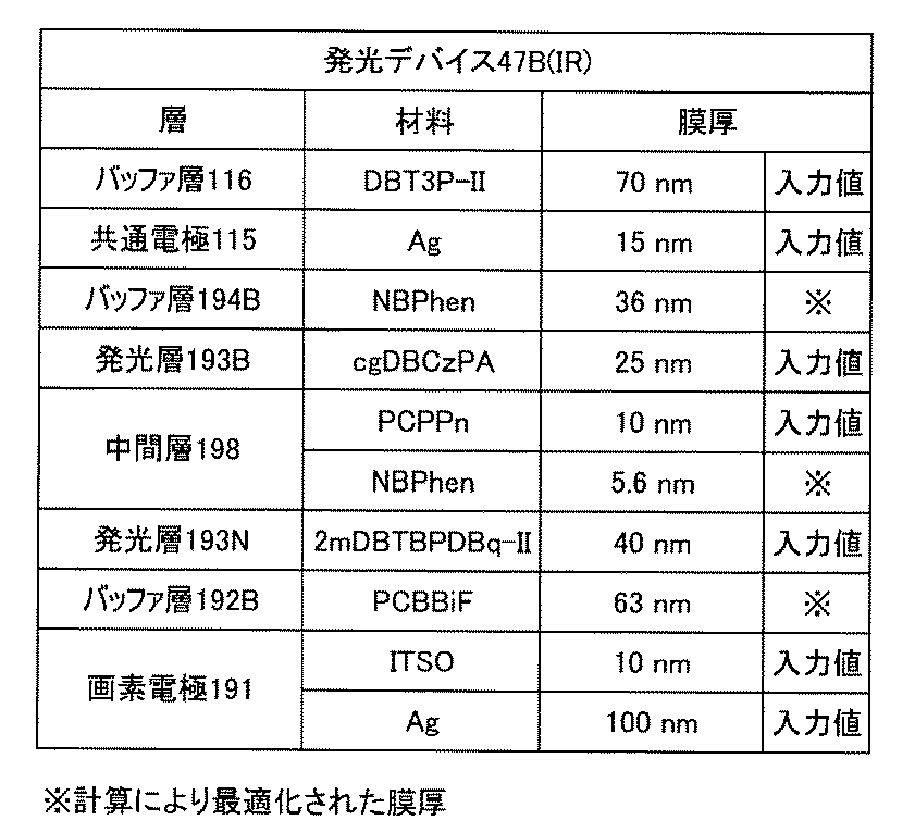


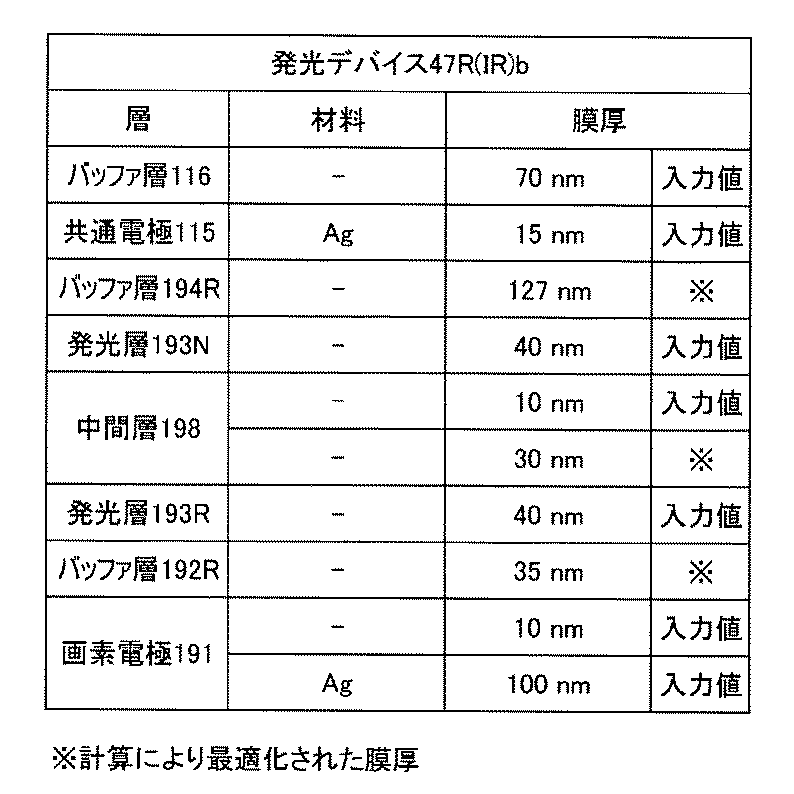
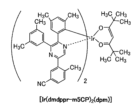

上記実施例1で用いたビス{4,6−ジメチル−2−[3−(3,5−ジメチルフェニル)−2−ベンゾ[g]キノキサリニル−κN]フェニル−κC}(2,2,6,6−テトラメチル−3,5−ヘプタンジオナト−κ2O,O’)イリジウム(III)(略称:[Ir(dmdpbq)2(dpm)])の合成方法について、具体的に説明する。[Ir(dmdpbq)2(dpm)]の構造を以下に示す。

まず、ステップ1では、Hdmdpbqを合成した。3,3’,5,5’−テトラメチルベンジル3.20g、2,3−ジアミノナフタレン1.97g、エタノール60mLを、還流管を付けた三口フラスコに入れ、内部を窒素置換した後、90℃で7時間半撹拌した。所定時間経過後、溶媒を留去した。その後、トルエンを展開溶媒とするシリカゲルカラムクロマトグラフィーで精製し、目的物を得た(黄色固体、収量3.73g、収率79%)。ステップ1の合成スキームを(a−1)に示す。
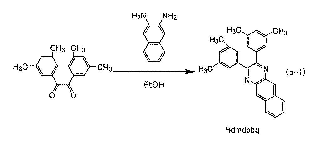
1H−NMR.δ(CD2Cl2):2.28(s,12H),7.01(s,2H),7.16(s,4H),7.56−7.58(m,2H),8.11−8.13(m,2H),8.74(s,2H).
次に、ステップ2では、[Ir(dmdpbq)2Cl]2を合成した。2−エトキシエタノール15mL、水5mL、ステップ1で得たHdmdpbq1.81g、及び、塩化イリジウム水和物(IrCl3・H2O)(フルヤ金属社製)0.66gを、還流管を付けたナスフラスコに入れ、フラスコ内をアルゴン置換した。その後、マイクロ波(2.45GHz 100W)を2時間照射し、反応させた。所定時間経過後、得られた残渣をメタノールで吸引ろ過、洗浄し、目的物を得た(黒色固体、収量1.76g、収率81%)。ステップ2の合成スキームを(a−2)に示す。

そして、ステップ3では、[Ir(dmdpbq)2(dpm)]を合成した。2−エトキシエタノール20mL、ステップ2で得た[Ir(dmdpbq)2Cl]21.75g、ジピバロイルメタン(略称:Hdpm)0.50g、及び、炭酸ナトリウム0.95gを、還流管を付けたナスフラスコに入れ、フラスコ内をアルゴン置換した。その後、マイクロ波(2.45GHz 100W)を3時間照射した。得られた残渣を、メタノールで吸引ろ過した後、水、メタノールで洗浄した。得られた固体を、ジクロロメタンを展開溶媒とするシリカゲルカラムクロマトグラフィーにより精製した後、ジクロロメタンとメタノールの混合溶媒にて再結晶することにより、目的物を得た(暗緑色固体、収量0.42g、収率21%)。得られた暗緑色固体0.41gを、トレインサブリメーション法により昇華精製した。昇華精製条件は、圧力2.7Pa、アルゴンガスを流量10.5mL/minで流しながら、300℃で暗緑色固体を加熱した。昇華精製後、暗緑色固体を収率78%で得た。ステップ3の合成スキームを(a−3)に示す。

Claims (39)
- 第1の発光デバイスと、第2の発光デバイスと、を有し、
前記第1の発光デバイスは、第1の画素電極、第1の発光層、第2の発光層、及び共通電極を有し、
前記第1の発光層及び前記第2の発光層は、それぞれ、前記第1の画素電極と前記共通電極との間に位置し、
前記第2の発光デバイスは、第2の画素電極、第3の発光層、及び前記共通電極を有し、
前記第3の発光層は、前記第2の画素電極と前記共通電極との間に位置し、
前記第1の発光層は、赤外光を発する発光材料を有し、
前記第2の発光層及び前記第3の発光層は、それぞれ異なる波長の可視光を発する発光材料を有する、発光装置。 - 請求項1において、
前記第1の発光層は、前記第1の画素電極と前記第2の発光層との間に位置する、発光装置。 - 請求項1または2において、
前記第1の画素電極は、可視光及び赤外光を反射する機能を有し、
前記共通電極は、可視光及び赤外光を透過する機能を有し、
前記第2の発光層は、青色の光を発する発光材料を有する、発光装置。 - 請求項1乃至3のいずれか一において、
前記第1の発光層は、ピーク波長λaの光を発し、
前記第2の発光層は、ピーク波長λbの光を発し、
前記第1の発光層の発光領域は、前記第1の画素電極からの光学距離がλa/4またはその近傍に位置し、
前記第2の発光層の発光領域は、前記第1の画素電極からの光学距離が3λb/4またはその近傍に位置する、発光装置。 - 請求項1乃至3のいずれか一において、
前記第1の発光デバイスは、さらに、正孔輸送層を有し、
前記第1の発光層は、ピーク波長λaの光を発し、
前記第2の発光層は、ピーク波長λbの光を発し、
前記正孔輸送層は、波長λbの光に対する常光屈折率が、波長λaの光に対する常光屈折率よりも0.1以上大きい、発光装置。 - 請求項1乃至3のいずれか一において、
前記第1の発光デバイスは、さらに、電子輸送層を有し、
前記第1の発光層は、ピーク波長λaの光を発し、
前記第2の発光層は、ピーク波長λbの光を発し、
前記電子輸送層は、波長λbの光に対する常光屈折率が、波長λaの光に対する常光屈折率よりも0.1以上大きい、発光装置。 - 請求項1において、
前記第2の発光層は、前記第1の画素電極と前記第1の発光層との間に位置する、発光装置。 - 請求項7において、
前記第1の画素電極は、可視光及び赤外光を透過する機能を有し、
前記共通電極は、可視光及び赤外光を反射する機能を有し、
前記第2の発光層は、青色の光を発する発光材料を有する、発光装置。 - 請求項7または8において、
前記第1の発光層は、ピーク波長λaの光を発し、
前記第2の発光層は、ピーク波長λbの光を発し、
前記第1の発光層の発光領域は、前記第1の画素電極からの光学距離が3λa/4またはその近傍に位置し、
前記第2の発光層の発光領域は、前記第1の画素電極からの光学距離がλb/4またはその近傍に位置する、発光装置。 - 請求項1乃至9のいずれか一において、
前記第1の発光デバイスは、可視光及び赤外光の双方を発する機能を有し、
前記第2の発光デバイスは、可視光を発する機能を有する、発光装置。 - 請求項1乃至10のいずれか一において、
前記第1の発光デバイスは、さらに、電荷発生層を有し、
前記電荷発生層は、前記第1の発光層と前記第2の発光層との間に位置する、発光装置。 - 請求項1乃至11のいずれか一において、
前記第1の発光デバイス及び前記第2の発光デバイスは、それぞれ、微小光共振器構造を有し、
前記第1の発光デバイスが有する前記微小光共振器構造は、赤色、緑色、または青色の光と、赤外光と、の双方を強める構成であり、
前記第2の発光デバイスが有する前記微小光共振器構造は、赤色、緑色、または青色の光を強める構成である、発光装置。 - 請求項1乃至12のいずれか一において、
さらに、第3の発光デバイスを有し、
前記第3の発光デバイスは、第3の画素電極、前記第1の発光層、前記第2の発光層、及び前記共通電極を有し、
前記第1の発光デバイス及び前記第3の発光デバイスは、それぞれ、微小光共振器構造を有し、
前記第1の発光デバイスが有する前記微小光共振器構造は、赤外光を強める構成であり、
前記第3の発光デバイスが有する前記微小光共振器構造は、赤色、緑色、または青色の光を強める構成である、発光装置。 - 請求項1乃至13のいずれか一において、
前記第1の発光デバイス及び前記第2の発光デバイスは、さらに、共通層を有し、
前記共通層は、前記第1の画素電極と前記共通電極との間に位置する領域と、前記第2の画素電極と前記共通電極との間に位置する領域と、を有する、発光装置。 - 表示部を有する表示装置であり、
前記表示部は、第1の発光デバイス、第2の発光デバイス、及び受光デバイスを有し、
前記第1の発光デバイスは、可視光及び赤外光の双方を発する機能を有し、
前記第2の発光デバイスは、可視光を発する機能を有し、
前記受光デバイスは、可視光及び赤外光のうち少なくとも一部を吸収する機能を有し、
前記第1の発光デバイスは、第1の画素電極、第1の発光層、第2の発光層、及び共通電極を有し、
前記第1の発光層及び前記第2の発光層は、それぞれ、前記第1の画素電極と前記共通電極との間に位置し、
前記第2の発光デバイスは、第2の画素電極、第3の発光層、及び前記共通電極を有し、
前記第3の発光層は、前記第2の画素電極と前記共通電極との間に位置し、
前記受光デバイスは、第3の画素電極、活性層、及び前記共通電極を有し、
前記活性層は、前記第3の画素電極と前記共通電極との間に位置し、
前記第1の発光層は、赤外光を発する発光材料を有し、
前記第2の発光層及び前記第3の発光層は、それぞれ異なる波長の可視光を発する発光材料を有し、
前記活性層は、有機化合物を有する、表示装置。 - 請求項15において、
前記第1の発光デバイスは、共通層を有し、
前記第2の発光デバイスは、前記共通層を有し、
前記受光デバイスは、前記共通層を有し、
前記共通層は、前記第1の画素電極と前記共通電極との間に位置する領域と、前記第2の画素電極と前記共通電極との間に位置する領域と、前記第3の画素電極と前記共通電極との間に位置する領域と、を有する、表示装置。 - 請求項15または16において、
前記第1の発光層は、前記第1の画素電極と前記第2の発光層との間に位置する、表示装置。 - 請求項15乃至17のいずれか一において、
前記第1の画素電極は、可視光及び赤外光を反射する機能を有し、
前記共通電極は、可視光及び赤外光を透過する機能を有し、
前記第2の発光層は、青色の光を発する発光材料を有する、表示装置。 - 請求項15乃至18のいずれか一において、
前記第1の発光層は、ピーク波長λaの光を発し、
前記第2の発光層は、ピーク波長λbの光を発し、
前記第1の発光層の発光領域は、前記第1の画素電極からの光学距離がλa/4またはその近傍に位置し、
前記第2の発光層の発光領域は、前記第1の画素電極からの光学距離が3λb/4またはその近傍に位置する、表示装置。 - 請求項15乃至19のいずれか一において、
前記第1の発光デバイスは、さらに、正孔輸送層を有し、
前記第1の発光層は、ピーク波長λaの光を発し、
前記第2の発光層は、ピーク波長λbの光を発し、
前記正孔輸送層は、波長λbの光に対する屈折率が、波長λaの光に対する屈折率よりも0.1以上大きい、表示装置。 - 請求項15乃至20のいずれか一において、
前記第1の発光デバイスは、さらに、電子輸送層を有し、
前記第1の発光層は、ピーク波長λaの光を発し、
前記第2の発光層は、ピーク波長λbの光を発し、
前記電子輸送層は、波長λbの光に対する屈折率が、波長λaの光に対する屈折率よりも0.1以上大きい、表示装置。 - 請求項15または16において、
前記第2の発光層は、前記第1の画素電極と前記第1の発光層との間に位置する、表示装置。 - 請求項22において、
前記第1の画素電極は、可視光及び赤外光を透過する機能を有し、
前記共通電極は、可視光及び赤外光を反射する機能を有し、
前記第2の発光層は、青色の光を発する発光材料を有する、表示装置。 - 請求項22または23において、
前記第1の発光層は、ピーク波長λaの光を発し、
前記第2の発光層は、ピーク波長λbの光を発し、
前記第1の発光層の発光領域は、前記第1の画素電極からの光学距離が3λa/4またはその近傍に位置し、
前記第2の発光層の発光領域は、前記第1の画素電極からの光学距離がλb/4またはその近傍に位置する、表示装置。 - 請求項15乃至24のいずれか一において、
前記第1の発光デバイスは、さらに、電荷発生層を有し、
前記電荷発生層は、前記第1の発光層と前記第2の発光層との間に位置する、表示装置。 - 請求項15乃至25のいずれか一において、
前記第1の発光デバイス及び前記第2の発光デバイスは、それぞれ、微小光共振器構造を有し、
前記第1の発光デバイスが有する前記微小光共振器構造は、赤色、緑色、または青色の光と、赤外光と、の双方を強める構成であり、
前記第2の発光デバイスが有する前記微小光共振器構造は、赤色、緑色、または青色の光を強める構成である、表示装置。 - 請求項15乃至26のいずれか一において、
さらに、第3の発光デバイスを有し、
前記第3の発光デバイスは、第4の画素電極、前記第1の発光層、前記第2の発光層、及び前記共通電極を有し、
前記第1の発光デバイス及び前記第3の発光デバイスは、それぞれ、微小光共振器構造を有し、
前記第1の発光デバイスが有する前記微小光共振器構造は、赤外光を強める構成であり、
前記第3の発光デバイスが有する前記微小光共振器構造は、赤色、緑色、または青色の光を強める構成である、表示装置。 - 請求項15乃至27のいずれか一において、
前記表示部は、可撓性を有する、表示装置。 - 請求項1乃至14のいずれか一に記載の発光装置、または、請求項15乃至28のいずれか一に記載の表示装置と、
コネクタまたは集積回路と、を有する、モジュール。 - 請求項29に記載のモジュールと、
アンテナ、バッテリ、筐体、カメラ、スピーカ、マイク、及び操作ボタンのうち、少なくとも一つと、を有する、電子機器。 - 第1の電極、第1の発光層、第2の発光層、及び第2の電極を有し、
前記第1の発光層及び前記第2の発光層は、それぞれ、前記第1の電極と前記第2の電極との間に位置し、
前記第1の発光層は、赤外光を発する発光材料を有し、
前記第2の発光層は、可視光を発する発光材料を有し、
赤外光及び可視光の双方を発する機能を有する、発光デバイス。 - 請求項31において、
前記第1の電極は、可視光及び赤外光を反射する機能を有し、
前記第2の電極は、可視光及び赤外光を透過する機能を有し、
前記第1の発光層は、前記第1の電極と前記第2の発光層との間に位置する、発光デバイス。 - 請求項32において、
前記第2の発光層は、青色の光を発する発光材料を有する、発光デバイス。 - 請求項31乃至33のいずれか一において、
前記第1の発光層は、ピーク波長λaの光を発し、
前記第2の発光層は、ピーク波長λbの光を発し、
前記第1の発光層の発光領域は、前記第1の電極からの光学距離がλa/4またはその近傍に位置し、
前記第2の発光層の発光領域は、前記第1の電極からの光学距離が3λb/4またはその近傍に位置する、発光デバイス。 - 請求項31乃至33のいずれか一において、
さらに、正孔輸送層を有し、
前記第1の発光層は、ピーク波長λaの光を発し、
前記第2の発光層は、ピーク波長λbの光を発し、
前記正孔輸送層は、波長λbの光に対する常光屈折率が、波長λaの光に対する常光屈折率よりも0.1以上大きい、発光デバイス。 - 請求項31乃至33のいずれか一において、
さらに、電子輸送層を有し、
前記第1の発光層は、ピーク波長λaの光を発し、
前記第2の発光層は、ピーク波長λbの光を発し、
前記電子輸送層は、波長λbの光に対する常光屈折率が、波長λaの光に対する常光屈折率よりも0.1以上大きい、発光デバイス。 - 請求項31において、
前記第1の電極は、可視光及び赤外光を反射する機能を有し、
前記第2の電極は、可視光及び赤外光を透過する機能を有し、
前記第2の発光層は、前記第1の電極と前記第1の発光層との間に位置する、発光デバイス。 - 請求項31乃至37のいずれか一において、
さらに、電荷発生層を有し、
前記電荷発生層は、前記第1の発光層と前記第2の発光層との間に位置する、発光デバイス。 - 請求項31乃至38のいずれか一において、
赤色、緑色、または青色の光と、赤外光と、の双方を強める構成の微小光共振器構造を有する、発光デバイス。
Priority Applications (9)
| Application Number | Priority Date | Filing Date | Title |
|---|---|---|---|
| CN202411380667.9A CN119277917A (zh) | 2018-12-21 | 2019-12-12 | 发光器件、发光装置、发光模块、照明装置、显示装置、显示模块及电子设备 |
| KR1020217021585A KR20210106475A (ko) | 2018-12-21 | 2019-12-12 | 발광 디바이스, 발광 장치, 발광 모듈, 조명 장치, 표시 장치, 표시 모듈, 및 전자 기기 |
| JP2020560640A JP7377216B2 (ja) | 2018-12-21 | 2019-12-12 | 表示装置、モジュール及び電子機器 |
| DE112019006355.3T DE112019006355T5 (de) | 2018-12-21 | 2019-12-12 | Licht emittierendes Gerät, Licht emittierende Vorrichtung, Licht emittierendes Modul, Beleuchtungsvorrichtung, Anzeigevorrichtung, Anzeigemodul und elektronisches Gerät |
| CN201980085307.7A CN113227728B (zh) | 2018-12-21 | 2019-12-12 | 发光器件、发光装置、发光模块、照明装置、显示装置、显示模块及电子设备 |
| US17/414,058 US12058878B2 (en) | 2018-12-21 | 2019-12-12 | Light-emitting device, light-emitting apparatus, light-emitting module, lighting device, display apparatus, display module, and electronic device |
| JP2023184650A JP7682973B2 (ja) | 2018-12-21 | 2023-10-27 | 発光装置、モジュール及び電子機器 |
| US18/791,891 US20240397741A1 (en) | 2018-12-21 | 2024-08-01 | Light-Emitting Device, Light-Emitting Apparatus, Light-Emitting Module, Lighting Device, Display Apparatus, Display Module, and Electronic Device |
| JP2025081361A JP2025114818A (ja) | 2018-12-21 | 2025-05-14 | 発光デバイス |
Applications Claiming Priority (4)
| Application Number | Priority Date | Filing Date | Title |
|---|---|---|---|
| JP2018-239832 | 2018-12-21 | ||
| JP2018-239835 | 2018-12-21 | ||
| JP2018239835 | 2018-12-21 | ||
| JP2018239832 | 2018-12-21 |
Related Child Applications (2)
| Application Number | Title | Priority Date | Filing Date |
|---|---|---|---|
| US17/414,058 A-371-Of-International US12058878B2 (en) | 2018-12-21 | 2019-12-12 | Light-emitting device, light-emitting apparatus, light-emitting module, lighting device, display apparatus, display module, and electronic device |
| US18/791,891 Continuation US20240397741A1 (en) | 2018-12-21 | 2024-08-01 | Light-Emitting Device, Light-Emitting Apparatus, Light-Emitting Module, Lighting Device, Display Apparatus, Display Module, and Electronic Device |
Publications (1)
| Publication Number | Publication Date |
|---|---|
| WO2020128735A1 true WO2020128735A1 (ja) | 2020-06-25 |
Family
ID=71102070
Family Applications (1)
| Application Number | Title | Priority Date | Filing Date |
|---|---|---|---|
| PCT/IB2019/060681 Ceased WO2020128735A1 (ja) | 2018-12-21 | 2019-12-12 | 発光デバイス、発光装置、発光モジュール、照明装置、表示装置、表示モジュール、及び電子機器 |
Country Status (7)
| Country | Link |
|---|---|
| US (2) | US12058878B2 (ja) |
| JP (3) | JP7377216B2 (ja) |
| KR (1) | KR20210106475A (ja) |
| CN (2) | CN113227728B (ja) |
| DE (1) | DE112019006355T5 (ja) |
| TW (1) | TWI846778B (ja) |
| WO (1) | WO2020128735A1 (ja) |
Cited By (8)
| Publication number | Priority date | Publication date | Assignee | Title |
|---|---|---|---|---|
| CN112018157A (zh) * | 2020-08-05 | 2020-12-01 | 武汉华星光电技术有限公司 | 显示装置 |
| CN112885883A (zh) * | 2021-01-28 | 2021-06-01 | 维沃移动通信有限公司 | 显示屏、显示屏的制作方法和电子设备 |
| JPWO2022053908A1 (ja) * | 2020-09-11 | 2022-03-17 | ||
| WO2022074499A1 (ja) * | 2020-10-09 | 2022-04-14 | 株式会社半導体エネルギー研究所 | 発光装置、電子機器および照明装置 |
| JPWO2022229781A1 (ja) * | 2021-04-30 | 2022-11-03 | ||
| JPWO2022248974A1 (ja) * | 2021-05-27 | 2022-12-01 | ||
| WO2023119050A1 (ja) * | 2021-12-23 | 2023-06-29 | 株式会社半導体エネルギー研究所 | 表示装置 |
| JP7863092B2 (ja) | 2021-04-30 | 2026-05-20 | 株式会社半導体エネルギー研究所 | 表示装置、及び表示装置の作製方法 |
Families Citing this family (10)
| Publication number | Priority date | Publication date | Assignee | Title |
|---|---|---|---|---|
| KR102877398B1 (ko) | 2019-07-26 | 2025-10-28 | 가부시키가이샤 한도오따이 에네루기 켄큐쇼 | 복합 디바이스 및 프로그램 |
| WO2021140404A1 (ja) | 2020-01-10 | 2021-07-15 | 株式会社半導体エネルギー研究所 | 電子機器、及びプログラム |
| CN111584597B (zh) * | 2020-05-26 | 2021-10-15 | 云谷(固安)科技有限公司 | 显示面板及显示装置 |
| CN115868248B (zh) * | 2020-08-04 | 2025-12-16 | 夏普株式会社 | 发光元件以及发光器件 |
| JP7808950B2 (ja) * | 2020-11-05 | 2026-01-30 | 株式会社半導体エネルギー研究所 | 発光デバイス、発光装置、電子機器、表示装置、照明装置 |
| TW202240886A (zh) | 2020-12-04 | 2022-10-16 | 日商半導體能源研究所股份有限公司 | 顯示面板、資料處理裝置及用於製造顯示面板之方法 |
| JP7773531B2 (ja) | 2021-04-22 | 2025-11-19 | 株式会社半導体エネルギー研究所 | 表示装置、及び表示装置の作製方法 |
| CN115000122A (zh) * | 2021-10-09 | 2022-09-02 | 荣耀终端有限公司 | 显示面板、显示装置及终端 |
| CN114659625B (zh) * | 2022-03-17 | 2023-04-25 | 电子科技大学 | 基于石墨烯机械振子的性能可调辐射热计及制备方法 |
| JP2024101303A (ja) * | 2023-01-17 | 2024-07-29 | キヤノン株式会社 | 発光素子 |
Citations (7)
| Publication number | Priority date | Publication date | Assignee | Title |
|---|---|---|---|---|
| JP2010050014A (ja) * | 2008-08-25 | 2010-03-04 | Seiko Epson Corp | 発光装置および電子機器 |
| JP2015162463A (ja) * | 2014-02-26 | 2015-09-07 | 三星ディスプレイ株式會社Samsung Display Co.,Ltd. | 有機発光表示装置 |
| US20150364527A1 (en) * | 2014-06-11 | 2015-12-17 | Samsung Display Co., Ltd. | Organic light emitting diode display including sensors |
| JP2016066626A (ja) * | 2015-12-22 | 2016-04-28 | セイコーエプソン株式会社 | 発光素子、発光装置および電子機器 |
| US20180261652A1 (en) * | 2017-03-08 | 2018-09-13 | Samsung Display Co., Ltd. | Light emitting display device |
| JP2018147877A (ja) * | 2017-03-08 | 2018-09-20 | 三星ディスプレイ株式會社Samsung Display Co.,Ltd. | 発光表示装置 |
| US20190096959A1 (en) * | 2017-09-25 | 2019-03-28 | Samsung Display Co., Ltd. | Light emitting display device |
Family Cites Families (29)
| Publication number | Priority date | Publication date | Assignee | Title |
|---|---|---|---|---|
| US7956349B2 (en) | 2001-12-05 | 2011-06-07 | Semiconductor Energy Laboratory Co., Ltd. | Organic semiconductor element |
| JP4522862B2 (ja) | 2002-11-13 | 2010-08-11 | 株式会社半導体エネルギー研究所 | キノキサリン誘導体、有機半導体素子および電界発光素子 |
| US7042444B2 (en) | 2003-01-17 | 2006-05-09 | Eastman Kodak Company | OLED display and touch screen |
| KR100700013B1 (ko) | 2004-11-26 | 2007-03-26 | 삼성에스디아이 주식회사 | 유기전계발광소자 및 그의 제조 방법 |
| JP2010153449A (ja) | 2008-12-24 | 2010-07-08 | Seiko Epson Corp | 光源一体型光電変換装置 |
| JP5790279B2 (ja) * | 2011-08-09 | 2015-10-07 | セイコーエプソン株式会社 | 発光素子、発光装置および電子機器 |
| WO2013038627A1 (ja) | 2011-09-12 | 2013-03-21 | 保土谷化学工業株式会社 | 有機エレクトロルミネッセンス素子 |
| JP5970811B2 (ja) | 2011-12-28 | 2016-08-17 | セイコーエプソン株式会社 | 発光素子、発光装置および電子機器 |
| KR102079188B1 (ko) | 2012-05-09 | 2020-02-19 | 가부시키가이샤 한도오따이 에네루기 켄큐쇼 | 발광 장치 및 전자 기기 |
| US9817520B2 (en) | 2013-05-20 | 2017-11-14 | Semiconductor Energy Laboratory Co., Ltd. | Imaging panel and imaging device |
| US20160141515A1 (en) | 2013-06-11 | 2016-05-19 | Idemitsu Kosan Co., Ltd. | Material for organic electroluminescent elements, organic electroluminescent element using same, and electronic device |
| WO2014199842A1 (en) | 2013-06-14 | 2014-12-18 | Semiconductor Energy Laboratory Co., Ltd. | Organometallic iridium complex, light-emitting element, light-emitting device, and lighting device |
| US9553274B2 (en) | 2013-07-16 | 2017-01-24 | Universal Display Corporation | Organic electroluminescent materials and devices |
| JP6424456B2 (ja) | 2013-07-17 | 2018-11-21 | セイコーエプソン株式会社 | 発光装置、発光装置の製造方法、受発光装置、電子機器 |
| KR102250186B1 (ko) | 2014-05-19 | 2021-05-10 | 삼성전자주식회사 | 축합환 화합물 및 이를 포함한 유기 발광 소자 |
| JP6459228B2 (ja) * | 2014-06-02 | 2019-01-30 | セイコーエプソン株式会社 | 発光装置、電子機器および検査方法 |
| JP6181116B2 (ja) | 2014-07-24 | 2017-08-16 | ドク サン ネオルクス カンパニー リミテッド | 有機電子素子及びこれを含む電子装置 |
| US9660220B2 (en) * | 2014-10-24 | 2017-05-23 | Semiconductor Energy Laboratory Co., Ltd. | Multiple light-emitting element device |
| GB2549246A (en) | 2015-12-15 | 2017-10-18 | Cambridge Display Tech Ltd | Light-emitting Compound |
| WO2018033820A1 (en) | 2016-08-17 | 2018-02-22 | Semiconductor Energy Laboratory Co., Ltd. | Organic compound, light-emitting element, light-emitting device, electronic device, and lighting device |
| CN110073510B (zh) | 2016-12-28 | 2022-07-19 | 株式会社半导体能源研究所 | 发光元件、有机化合物、发光装置、电子设备及照明装置 |
| CN108341806B (zh) | 2017-01-22 | 2020-09-22 | 清华大学 | 铱金属配合物及其应用,以及有机电致发光器件 |
| JP7043733B2 (ja) | 2017-03-13 | 2022-03-30 | セイコーエプソン株式会社 | 発光素子、発光装置、光源、認証装置および電子機器 |
| US20190031673A1 (en) | 2017-07-27 | 2019-01-31 | Semiconductor Energy Laboratory Co., Ltd. | Organic Compound, Light-Emitting Element, Light-Emitting Device, Electronic Device, and Lighting Device |
| CN111033785B (zh) * | 2017-08-24 | 2023-04-25 | Agc株式会社 | 有机光电子元件 |
| US20190062357A1 (en) | 2017-08-28 | 2019-02-28 | Samsung Display Co., Ltd. | Organometallic compound, organic light-emitting device including the organometallic compound, and organic light-emitting apparatus including the organic light-emitting device |
| CN117715451A (zh) * | 2017-09-12 | 2024-03-15 | 株式会社半导体能源研究所 | 发光元件、发光装置、电子设备及照明装置 |
| KR20190049958A (ko) | 2017-10-30 | 2019-05-10 | 삼성디스플레이 주식회사 | 축합환 화합물 및 이를 포함한 유기 발광 소자 |
| JP2019102153A (ja) * | 2017-11-29 | 2019-06-24 | 株式会社ジャパンディスプレイ | 発光素子、および表示装置 |
-
2019
- 2019-12-12 DE DE112019006355.3T patent/DE112019006355T5/de active Pending
- 2019-12-12 TW TW108145479A patent/TWI846778B/zh active
- 2019-12-12 US US17/414,058 patent/US12058878B2/en active Active
- 2019-12-12 CN CN201980085307.7A patent/CN113227728B/zh active Active
- 2019-12-12 CN CN202411380667.9A patent/CN119277917A/zh active Pending
- 2019-12-12 JP JP2020560640A patent/JP7377216B2/ja active Active
- 2019-12-12 WO PCT/IB2019/060681 patent/WO2020128735A1/ja not_active Ceased
- 2019-12-12 KR KR1020217021585A patent/KR20210106475A/ko active Pending
-
2023
- 2023-10-27 JP JP2023184650A patent/JP7682973B2/ja active Active
-
2024
- 2024-08-01 US US18/791,891 patent/US20240397741A1/en active Pending
-
2025
- 2025-05-14 JP JP2025081361A patent/JP2025114818A/ja active Pending
Patent Citations (7)
| Publication number | Priority date | Publication date | Assignee | Title |
|---|---|---|---|---|
| JP2010050014A (ja) * | 2008-08-25 | 2010-03-04 | Seiko Epson Corp | 発光装置および電子機器 |
| JP2015162463A (ja) * | 2014-02-26 | 2015-09-07 | 三星ディスプレイ株式會社Samsung Display Co.,Ltd. | 有機発光表示装置 |
| US20150364527A1 (en) * | 2014-06-11 | 2015-12-17 | Samsung Display Co., Ltd. | Organic light emitting diode display including sensors |
| JP2016066626A (ja) * | 2015-12-22 | 2016-04-28 | セイコーエプソン株式会社 | 発光素子、発光装置および電子機器 |
| US20180261652A1 (en) * | 2017-03-08 | 2018-09-13 | Samsung Display Co., Ltd. | Light emitting display device |
| JP2018147877A (ja) * | 2017-03-08 | 2018-09-20 | 三星ディスプレイ株式會社Samsung Display Co.,Ltd. | 発光表示装置 |
| US20190096959A1 (en) * | 2017-09-25 | 2019-03-28 | Samsung Display Co., Ltd. | Light emitting display device |
Cited By (17)
| Publication number | Priority date | Publication date | Assignee | Title |
|---|---|---|---|---|
| CN112018157A (zh) * | 2020-08-05 | 2020-12-01 | 武汉华星光电技术有限公司 | 显示装置 |
| US12150367B2 (en) | 2020-09-11 | 2024-11-19 | Semiconductor Energy Laboratory Co., Ltd. | Display device, display module, and electronic device |
| US12620258B2 (en) | 2020-09-11 | 2026-05-05 | Semiconductor Energy Laboratory Co., Ltd. | Display device, display module, and electronic device |
| JPWO2022053908A1 (ja) * | 2020-09-11 | 2022-03-17 | ||
| WO2022053908A1 (ja) * | 2020-09-11 | 2022-03-17 | 株式会社半導体エネルギー研究所 | 表示装置、表示モジュール、及び電子機器 |
| JP7671302B2 (ja) | 2020-09-11 | 2025-05-01 | 株式会社半導体エネルギー研究所 | 表示装置、表示モジュール、及び電子機器 |
| WO2022074499A1 (ja) * | 2020-10-09 | 2022-04-14 | 株式会社半導体エネルギー研究所 | 発光装置、電子機器および照明装置 |
| JPWO2022074499A1 (ja) * | 2020-10-09 | 2022-04-14 | ||
| US12272302B2 (en) | 2021-01-28 | 2025-04-08 | Vivo Mobile Communication Co., Ltd. | Display, display fabrication method, and electronic device |
| CN112885883A (zh) * | 2021-01-28 | 2021-06-01 | 维沃移动通信有限公司 | 显示屏、显示屏的制作方法和电子设备 |
| WO2022229781A1 (ja) * | 2021-04-30 | 2022-11-03 | 株式会社半導体エネルギー研究所 | 表示装置、及び表示装置の作製方法 |
| JPWO2022229781A1 (ja) * | 2021-04-30 | 2022-11-03 | ||
| JP7863092B2 (ja) | 2021-04-30 | 2026-05-20 | 株式会社半導体エネルギー研究所 | 表示装置、及び表示装置の作製方法 |
| WO2022248974A1 (ja) * | 2021-05-27 | 2022-12-01 | 株式会社半導体エネルギー研究所 | 表示装置 |
| JPWO2022248974A1 (ja) * | 2021-05-27 | 2022-12-01 | ||
| JP7827715B2 (ja) | 2021-05-27 | 2026-03-10 | 株式会社半導体エネルギー研究所 | 表示装置 |
| WO2023119050A1 (ja) * | 2021-12-23 | 2023-06-29 | 株式会社半導体エネルギー研究所 | 表示装置 |
Also Published As
| Publication number | Publication date |
|---|---|
| US12058878B2 (en) | 2024-08-06 |
| DE112019006355T5 (de) | 2021-09-02 |
| US20220029121A1 (en) | 2022-01-27 |
| TW202033054A (zh) | 2020-09-01 |
| JPWO2020128735A1 (ja) | 2020-06-25 |
| JP2023181340A (ja) | 2023-12-21 |
| JP2025114818A (ja) | 2025-08-05 |
| CN119277917A (zh) | 2025-01-07 |
| TW202437808A (zh) | 2024-09-16 |
| CN113227728B (zh) | 2024-10-29 |
| US20240397741A1 (en) | 2024-11-28 |
| CN113227728A (zh) | 2021-08-06 |
| TWI846778B (zh) | 2024-07-01 |
| JP7682973B2 (ja) | 2025-05-26 |
| JP7377216B2 (ja) | 2023-11-09 |
| KR20210106475A (ko) | 2021-08-30 |
Similar Documents
| Publication | Publication Date | Title |
|---|---|---|
| JP7650327B2 (ja) | 発光装置 | |
| JP7682973B2 (ja) | 発光装置、モジュール及び電子機器 | |
| JP7574352B2 (ja) | 電子デバイス、表示装置、電子機器、及び照明装置 | |
| US11387280B2 (en) | Light-emitting device and electronic device | |
| KR102717448B1 (ko) | 발광 소자, 발광 장치, 전자 기기, 및 조명 장치 | |
| JP2024156928A (ja) | 発光素子 | |
| KR20210004867A (ko) | 표시 장치, 표시 모듈, 및 전자 기기 | |
| US20230276647A1 (en) | Light-emitting device, light-emitting apparatus, light-emitting module, electronic device, and lighting device | |
| US20230225149A1 (en) | Composite material for hole-injection layer, optical device, apparatus, module, electronic device, and lighting device | |
| TWI917966B (zh) | 發光器件、發光裝置、發光模組、照明裝置、顯示裝置、顯示模組及電子機器 | |
| TWI925706B (zh) | 發光裝置、照明裝置、顯示裝置、模組及電子機器 | |
| KR20260013414A (ko) | 발광 디바이스 |
Legal Events
| Date | Code | Title | Description |
|---|---|---|---|
| 121 | Ep: the epo has been informed by wipo that ep was designated in this application |
Ref document number: 19900428 Country of ref document: EP Kind code of ref document: A1 |
|
| ENP | Entry into the national phase |
Ref document number: 2020560640 Country of ref document: JP Kind code of ref document: A |
|
| ENP | Entry into the national phase |
Ref document number: 20217021585 Country of ref document: KR Kind code of ref document: A |
|
| 122 | Ep: pct application non-entry in european phase |
Ref document number: 19900428 Country of ref document: EP Kind code of ref document: A1 |