WO2020121832A1 - 光接続構造 - Google Patents
光接続構造 Download PDFInfo
- Publication number
- WO2020121832A1 WO2020121832A1 PCT/JP2019/046616 JP2019046616W WO2020121832A1 WO 2020121832 A1 WO2020121832 A1 WO 2020121832A1 JP 2019046616 W JP2019046616 W JP 2019046616W WO 2020121832 A1 WO2020121832 A1 WO 2020121832A1
- Authority
- WO
- WIPO (PCT)
- Prior art keywords
- optical
- waveguide
- connection structure
- support
- optical connection
- Prior art date
- Legal status (The legal status is an assumption and is not a legal conclusion. Google has not performed a legal analysis and makes no representation as to the accuracy of the status listed.)
- Ceased
Links
Images





Classifications
-
- G—PHYSICS
- G02—OPTICS
- G02B—OPTICAL ELEMENTS, SYSTEMS OR APPARATUS
- G02B6/00—Light guides; Structural details of arrangements comprising light guides and other optical elements, e.g. couplings
- G02B6/24—Coupling light guides
- G02B6/26—Optical coupling means
- G02B6/30—Optical coupling means for use between fibre and thin-film device
-
- G—PHYSICS
- G02—OPTICS
- G02B—OPTICAL ELEMENTS, SYSTEMS OR APPARATUS
- G02B6/00—Light guides; Structural details of arrangements comprising light guides and other optical elements, e.g. couplings
- G02B6/24—Coupling light guides
- G02B6/26—Optical coupling means
- G02B6/30—Optical coupling means for use between fibre and thin-film device
- G02B6/305—Optical coupling means for use between fibre and thin-film device and having an integrated mode-size expanding section, e.g. tapered waveguide
-
- G—PHYSICS
- G02—OPTICS
- G02B—OPTICAL ELEMENTS, SYSTEMS OR APPARATUS
- G02B6/00—Light guides; Structural details of arrangements comprising light guides and other optical elements, e.g. couplings
- G02B6/10—Light guides; Structural details of arrangements comprising light guides and other optical elements, e.g. couplings of the optical waveguide type
- G02B6/12—Light guides; Structural details of arrangements comprising light guides and other optical elements, e.g. couplings of the optical waveguide type of the integrated circuit kind
- G02B6/122—Basic optical elements, e.g. light-guiding paths
- G02B6/1223—Basic optical elements, e.g. light-guiding paths high refractive index type, i.e. high-contrast waveguides
Definitions
- the present invention relates to an optical connection structure for coupling optical waveguides having different mode fields.
- a waveguide (hereinafter, also referred to as Si waveguide) is configured by a core made of silicon (Si) and a clad made of quartz (SiO 2 ).
- Si waveguide is configured by a core made of silicon (Si) and a clad made of quartz (SiO 2 ).
- Si silicon
- SiO 2 quartz
- FIG. 11 illustrates a conventional optical connection structure for coupling between optical waveguides having different mode fields.
- the Si waveguide 1 has a taper structure in which the core cross-sectional area monotonically decreases in the light propagation direction (see, for example, Non-Patent Document 1), and the Si waveguide 1 and the optical fiber 2 are resin-bonded. Bonded by material 3.
- the resin adhesive material 3 functions as an optical connection structure.
- the resin adhesive material 3 will be referred to as a conventional optical connection structure 100'.
- the Si waveguide 1 is composed of a core (Si waveguide core) 1-1 and a clad (Si waveguide clad) 1-2, and the optical fiber 2 is a core (fiber core) 2-1 and a clad (fiber clad). 2-2 and 2).
- the Si waveguide core 1-1 has a taper structure in which the cross-sectional area thereof is monotonically decreased in the light propagation direction.
- the optical axis of the Si waveguide 1 and the optical axis of the optical fiber 2 are adjusted in position so that they coincide with each other.
- the mode field of the Si waveguide 1 and the mode field of the optical fiber 2 are different due to variations in the fabrication of the tip of the Si waveguide core 1-1 having a tapered structure. And may not combine well.
- FIGS. 12A and 12B exemplify the waveguide distribution between the Si waveguide 1 and the optical fiber 2 in FIG. 12A shows the normalized power distribution seen from the y-axis direction
- FIG. 12B shows the mode field distribution (solid line) in the optical fiber plane obtained based on the waveguide analysis.
- the light emitted from the end surface of the Si waveguide 1 contains a large amount of radiation mode light propagating in the direction away from the optical axis. Therefore, due to variations in fabrication of the tip of the Si waveguide core 1-1 having a tapered structure, the coupling efficiency with the optical fiber 2 is reduced as a result. In this example, the coupling efficiency CE has dropped to -1.4 dB.
- the present invention has been made to solve such problems, and an object thereof is to provide an optical connection structure capable of improving the coupling efficiency between optical waveguides having different mode fields. is there.
- the present invention provides an optical connection structure (100) for coupling between a first optical waveguide (1) and a second optical waveguide (2) having different mode fields.
- a part of light in a radiation mode which is provided in a light propagation path between the first optical waveguide and the second optical waveguide and which is emitted from the first optical waveguide and propagates in a direction away from the optical axis. It is characterized by including an optical body (10) which changes the course of the light and changes it into light of a guided mode that passes through itself.
- the optical body changes the path of a part of the radiation mode light emitted from the first optical waveguide and propagating in the direction away from the optical axis, and makes it the guided mode light passing therethrough. .. This increases the amount of guided mode light that is incident on the second optical waveguide, and improves the coupling efficiency between the first optical waveguide and the second optical waveguide.
- the light in the light propagation path between the first optical waveguide and the second optical waveguide, the light is emitted from the first optical waveguide and propagates away from the optical axis.
- the path of a part of the radiation mode light to be changed is provided so as to provide the optical body that makes the guided mode light passing therethrough, so that the number of the guided mode light incident on the second optical waveguide is increased. In this way, the coupling efficiency between the optical waveguides having different mode fields can be improved.
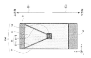
- FIG. 1A is a side view schematically showing an optical connection structure according to an embodiment of the present invention.
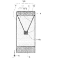
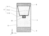
- 1B is a cross-sectional view taken along the line Ib-Ib in FIG. 1A.
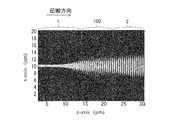
- FIG. 2A is a diagram exemplifying a waveguide distribution between a Si waveguide and an optical fiber using this optical connection structure.
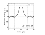
- FIG. 2B is a diagram illustrating a waveguide distribution between a Si waveguide and an optical fiber using this optical connection structure.
- FIG. 3 is a diagram showing an example in which an optical body is composed of a plurality of optical bodies arranged in an array.
- FIG. 4 is a diagram showing an example in which the support has a curved shape.
- FIG. 1A is a side view schematically showing an optical connection structure according to an embodiment of the present invention.
- 1B is a cross-sectional view taken along the line Ib-Ib in FIG. 1A.
- FIG. 2A is a diagram exemplifying a waveguide distribution between a
- FIG. 5 is a diagram showing an example in which an optical body is joined to the lower surface of the support body.
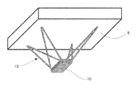
- FIG. 6 is a perspective view showing an example in which a support having a truss structure is provided.
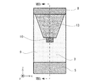
- FIG. 7 is a diagram showing an example in which a frustum-shaped support is provided.
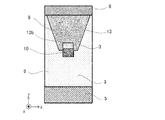
- FIG. 8A is a diagram showing an example in which a void (recess) is provided in the central portion of the lower surface of a frustum-shaped support body.
- 8B is a sectional view taken along line VIIIb-VIIIb of FIG. 8A.
- FIG. 9 is a diagram showing an example in which the support is a columnar three-dimensional object.
- FIG. 10 is a diagram showing an example in which the support body is a mountain-shaped three-dimensional object.
- FIG. 11 is a diagram illustrating a conventional optical connection structure.
- FIG. 12A is a diagram illustrating a waveguide distribution between a Si waveguide and an optical fiber in a conventional optical connection structure.
- FIG. 12B is a diagram illustrating the waveguide distribution between the Si waveguide and the optical fiber in the conventional optical connection structure.
- FIGS. 1A and 1B are schematic views showing an optical connection structure according to an embodiment of the present invention
- FIG. 1A is a side view
- FIG. 1B is a sectional view taken along line Ib-Ib in FIG. 1A.
- the same components as those described with reference to FIG. 11 are designated by the same reference numerals, and overlapping description will be omitted.
- the direction indicated by arrow 201 is the upward direction
- the direction indicated by arrow 202 is the downward direction.
- the Si waveguide 1 and the optical fiber 2 are position-adjusted so that the optical axis of the Si waveguide 1 and the optical axis of the optical fiber 2 coincide with each other, and the waveguide fixing base is also provided. 4 and an optical axis adjusting base 5 having a V groove and the like.
- a block 6 is bonded to the upper surface of the Si waveguide 1, that is, the upper surface of the Si waveguide cladding 1-2, and a block 7 is bonded to the upper surface of the optical fiber 2, that is, the upper surface of the fiber cladding 2-2. Further, part of the lower surface of the plate-shaped bridge body 8 is joined to the upper surfaces of the blocks 6 and 7, and the bridge body 8 is bridged between the blocks 6 and 7.
- the material for the blocks 6 and 7 is preferably a waveguide fixing adhesive with a small coefficient of thermal expansion.
- the blocks 6 and 7 are responsible for fixing and supporting the bridge 8.
- the thicknesses of the blocks 6 and 7 are such that the bridge body 8 is supported horizontally and that the optical axis of the optical body 10 described later, the optical axis of the Si waveguide 1 and the optical axis of the optical fiber 2 coincide with each other.
- the material of the bridge body 8 can be a material having high thermal conductivity (for example, silicon).
- the Si waveguide 1 between the end face of the Si waveguide 1 and the end face of the optical fiber 2, the Si waveguide 1, the waveguide fixing base 4, the block 6, the optical fiber 2, the optical axis adjusting base 5, and the block 7 are provided.
- the optical body 10 has a rectangular parallelepiped shape and is supported by a bridge body 8 that is bridged between the Si waveguide 1 and the optical fiber 2 via a support body 11.
- the optical body 10 and the support 11 are made of a photocurable resin and are integrated members.
- the bridge body 8 that is bridged between the block 6 and the block 7 is used as a substrate and is manufactured using an optical modeling apparatus.
- the hollow region 9 is filled with an epoxy-based or acrylic-based resin adhesive material 3.
- the optical body 10 is supported by the bridge body 8 via the support body 11 so that the optical axis of the optical body 10, the optical axis of the Si waveguide 1 and the optical axis of the optical fiber 2 coincide with each other.
- the length of the optical body 10 in the z direction is 2.5 ⁇ m
- the length (width) in the x direction is 2.0 ⁇ m
- the length (height) in the y direction is 2.0 ⁇ m.
- the length of the hollow region 9 in the z direction is 3 ⁇ m
- the support 11 is composed of a first support 11-1 and a second support 11-2, which are arranged to face each other along the optical axis of the optical body 10.
- the first support 11-1 and the second support 11-2 have a flat plate shape, and at one end of one side of the first support 11-1 and the second support 11-2 (
- the optical body 10 is formed at the lowermost portion, and the ends (uppermost portion) of the first support 11-1 and the second support 11-2 on the other side are joined to the bridge 8.
- the distance between the first support 11-1 and the second support 11-2 is narrowed from the bridge 8 toward the optical body 10.
- the distance between the first supporting body 11-1 and the second supporting body 11-2 at the connection position with the optical body 10 is not more than the width of the optical body 10 in the x direction.
- the length of the first support 11-1 and the second support 11-2 in the z direction is preferably smaller than the length of the optical body 10 in the z direction.
- connection structure between the Si waveguide 1 and the optical fiber 2 a support body 11 having one end portion joined to the bridge body 8 and an optical body formed at the other end portion of the support body 11 are provided.
- the optical connection structure 100 according to the present embodiment is constituted by the hollow region 9 in which the optical body 10 and the support 11 are provided, and the resin adhesive material 3 filled in the hollow region 9. There is.
- the Si waveguide 1 is assumed to have a taper structure in which the core cross-sectional area monotonically decreases in the light propagation direction, but the core cross-sectional area may be constant.
- the cross section of the Si waveguide core 1-1 perpendicular to the optical axis is rectangular, and the length (height) in the y direction of its emission end face is 0.2 ⁇ m and the length (width) in the x direction is 0. It is assumed to be 0.5 ⁇ m. Further, it is assumed that the fiber core 2-1 of the optical fiber 2 is thinned in the vicinity of the incident end face and has a diameter of 4 ⁇ m. The propagation wavelength is 1.55 ⁇ m.
- FIG. 2A and 2B exemplify the waveguide distribution between the Si waveguide 1 and the optical fiber 2 using this optical connection structure 100.
- FIG. 2A shows the normalized power distribution seen from the y-axis direction
- FIG. 2B shows the mode field distribution (solid line) in the optical fiber plane obtained based on the waveguide analysis.
- the optical body 10 provided in the light propagation path between the Si waveguide 1 and the optical fiber 2 causes the light to be emitted from the Si waveguide 1 and separated from the optical axis.
- the path of a part of the radiation mode light propagating in some direction is changed to be guided mode light passing through the optical body 10 itself.
- the amount of guided mode light incident on the optical fiber 2 increases, and the coupling efficiency between the Si waveguide 1 and the optical fiber 2 improves.
- the mode field distribution in the fiber plane was shaped, and the coupling efficiency CE was improved to ⁇ 0.069 dB. That is, in the conventional optical connection structure 100', the coupling efficiency CE was -1.4 dB (Fig. 12B), whereas in the optical connection structure 100 according to the present embodiment, it was improved to -0.069 dB.
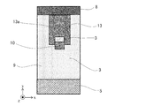
- the optical body 10 has a rectangular parallelepiped shape in the above-described embodiment, it may have a hexahedral shape or the like, and may have a shape such that the area of the surface perpendicular to the optical axis toward the optical fiber 2 decreases. Absent. Further, as shown in FIG. 3, the optical body 10 may be composed of a plurality of optical bodies 10a arranged in an array in the xy direction. Further, as shown in FIG. 4, the supports 11-1 and 11-2 may have a curved shape instead of a flat plate shape. As shown in FIG. 5, the support 11 has a flat bottom surface 11-3 that integrally connects the support 11-1 and the support 11-2. You may make it join the optical body 10 to 3. It should be noted that FIGS. 3, 4, 5 and FIGS. 7, 9 and 10 described later correspond to FIG. 1B, respectively.
- a support body 12 having a truss structure (structure type in which members are connected to each other in a triangle) may be provided instead of the support body 11, and the optical body 10 may be bonded to the lower surface of the support body 13.
- a void 13a penetrating in the z direction is formed on the lower surface of the support 13, and the optical body 10 is bonded to the lower side of this void 13a.
- the resin adhesive material 3 is filled in the void 13a.
- a void (recess) 13b is provided in the central portion of the lower surface of the frustum-shaped support 13 and the optical body 10 is bonded to the lower side of the void 13b.
- Good. 8A is a view of the support 13 as viewed from the z direction
- FIG. 8B is a cross-sectional view taken along the line VIIIb-VIIIb of FIG. 8A.
- the voids 13b are filled with the resin adhesive material 3, but the voids 13b do not necessarily have to be filled with the resin adhesive material 3. That is, the upper portion of the optical body 10 may be a free space.
- the radiation mode light emitted from the Si waveguide 1 and propagating in a direction away from the optical axis passes through the support 13.
- the light passes through the space 13b to pass therethrough, and a part of the light is changed in its course to be guided-mode light passing through the optical body 10 itself. If the void 13b does not exist, its course cannot be changed, and the light does not become a guided mode light passing through the optical body 10 itself. Therefore, it is necessary to provide the void 13b in the upper part of the optical body 10.
- the support 13 has a frustum shape, but the support 13 may be a three-dimensional object having two or more surfaces, and a cylindrical three-dimensional object as shown in FIG. Alternatively, a mountain-shaped three-dimensional object as shown in FIG. 10 may be used.
- the hollow area 9 is filled with the resin adhesive material 3, but the hollow area 9 may not necessarily be filled with the resin adhesive material 3.
Landscapes
- Physics & Mathematics (AREA)
- General Physics & Mathematics (AREA)
- Optics & Photonics (AREA)
- Engineering & Computer Science (AREA)
- Microelectronics & Electronic Packaging (AREA)
- Optical Couplings Of Light Guides (AREA)
Abstract
Si導波路1と光ファイバ2との間の光の伝搬路に光学体10を設ける。光学体10は、Si導波路1から出射され光軸から離れていく方向に伝搬する放射モードの光の一部の進路を変えて、自身を通過する導波モードの光とする。これにより、光ファイバ2に入射される導波モードの光が増え、Si導波路1と光ファイバ2との間の結合効率が向上する。これにより、異なるモードフィールドを有する光導波路間の結合効率を向上させる。
Description
本発明は、異なるモードフィールドを有する光導波路間を結合する光接続構造に関する。
近年、シリコン基板上に光電子デバイスを一括して集積する技術として、「シリコンフォトニクス」と呼ばれる技術が注目されている。シリコンフォトニクスでは、シリコン(Si)から形成されるコアと、石英(SiO2)から形成されるクラッドによって導波路(以下、Si導波路ともいう。)を構成している。Si導波路の導波光を光ファイバを介して高い結合効率で伝送するには、Si導波路のモードフィールドと光ファイバのモードフィールドとを整合させる光接続構造が必要となる。
図11に、異なるモードフィールドを有する光導波路間を結合する従来の光接続構造を例示する。この例では、Si導波路1のコア断面積を光の伝搬方向に向かって単調減少させたテーパ構造とし(例えば、非特許文献1参照。)、Si導波路1と光ファイバ2とを樹脂接着材料3によって結合させている。この例では、樹脂接着材料3が光接続構造として機能する。以下、樹脂接着材料3を従来の光接続構造100’とする。
なお、図11において、z軸は光の伝搬方向(光軸に沿った方向)を示し、y軸は鉛直方向、x軸は水平方向を示している。また、Si導波路1はコア(Si導波路コア)1-1とクラッド(Si導波路クラッド)1-2とから構成され、光ファイバ2はコア(ファイバコア)2-1とクラッド(ファイバクラッド)2-2とから構成されている。Si導波路1において、Si導波路コア1-1は、その断面積を光の伝搬方向に向かって単調減少させたテーパ構造とされている。また、Si導波路1の光軸と光ファイバ2の光軸とは、一致するように位置調整されている。
Yin Xiaojie, "Design and Simulation Analysis of Spot-Size Converter in Silicon-On-Insulator", CLEO/Pacific Rim 2009
しかしながら、図11に示した従来の光接続構造100’では、テーパ構造とされたSi導波路コア1-1の先端の作製ばらつき等により、Si導波路1のモードフィールドと光ファイバ2のモードフィールドとが十分に結合しない場合がある。
図12Aおよび図12Bに、図11におけるSi導波路1と光ファイバ2との間の導波分布を例示する。図12Aは、y軸方向から見た規格化電力分布を示し、図12Bは導波解析を基に得られた光ファイバ面内のモードフィールド分布(実線)を示している。図12Aおよび図12Bに示すように、Si導波路1の端面から出射される光は、光軸から離れていく方向に伝搬する放射モードの光を多く含む。このため、テーパ構造とされたSi導波路コア1-1の先端の作製ばらつき等により、結果として光ファイバ2との結合効率が低下する。この例において、結合効率CEは、-1.4dBまで低下している。
本発明は、このような課題を解決するためになされたもので、その目的とするところは、異なるモードフィールドを有する光導波路間の結合効率を向上させることができる光接続構造を提供することにある。
このような目的を達成するために本発明は、異なるモードフィールドを有する第1の光導波路(1)と第2の光導波路(2)との間を結合する光接続構造(100)において、前記第1の光導波路と前記第2の光導波路との間の光の伝搬路に設けられ、前記第1の光導波路から出射され光軸から離れていく方向に伝搬する放射モードの光の一部の進路を変えて、自身を通過する導波モードの光とする光学体(10)を備えることを特徴とする。
本発明において、光学体は、第1の光導波路から出射され光軸から離れていく方向に伝搬する放射モードの光の一部の進路を変えて、自身を通過する導波モードの光とする。これにより、第2の光導波路に入射される導波モードの光が増え、第1の光導波路と第2の光導波路との間の結合効率が向上する。
なお、上記説明では、一例として、発明の構成要素に対応する図面上の構成要素を、括弧を付した参照符号によって示している。
以上説明したように、本発明によれば、第1の光導波路と第2の光導波路との間の光の伝搬路に、第1の光導波路から出射され光軸から離れていく方向に伝搬する放射モードの光の一部の進路を変えて、自身を通過する導波モードの光とする光学体を設けるようにしたので、第2の光導波路に入射される導波モードの光を増やすようにして、異なるモードフィールドを有する光導波路間の結合効率を向上させることができるようになる。
以下、本発明の実施の形態を図面に基づいて詳細に説明する。
図1Aおよび図1Bは本発明の実施の形態に係る光接続構造を示す模式図であり、図1Aは側面図、図1Bは図1AのIb-Ib線における断面図である。図1Aおよび図1Bにおいて、図11を参照して説明した構成要素と同一の構成要素については同一の符号を付し、重複する説明は省略する。また、図1Aおよび図1Bにおいて、矢印201で示される方向を上方向、矢印202で示される方向を下方向とする。
図1Aおよび図1Bにおいて、Si導波路1と光ファイバ2とは、Si導波路1の光軸と光ファイバ2の光軸とが一致するように位置調整されたうえ、導波路固定用基台4とV溝等を有する光軸調整用基台5とにそれぞれ固定されている。
Si導波路1の上面、すなわちSi導波路クラッド1-2の上面にはブロック6が接合され、光ファイバ2の上面、すなわちファイバクラッド2-2の上面にはブロック7が接合されている。さらに、ブロック6とブロック7の上面には板状の橋体8の下面の一部が接合されて、ブロック6とブロック7との間に橋体8が架け渡されている。
なお、ブロック6,7の材料は、熱膨張係数が小さい導波路固定用接着剤が望ましい。このブロック6,7が橋体8の固定と支持を担う。ブロック6,7の厚みは、橋体8が水平に支持されるように、かつ、後述する光学体10の光軸とSi導波路1の光軸と光ファイバ2の光軸とが一致するように、調整される。例えば、橋体8の材料は、熱伝導性の高い材料(例えば、シリコン)とすることができる。
また、Si導波路1の端面と光ファイバ2の端面との間には、Si導波路1と導波路固定用基台4とブロック6と光ファイバ2と光軸調整用基台5とブロック7と橋体8とで囲まれる中空の領域(以下、「中空領域」と呼ぶ。)9が形成されており、この中空領域9内にコアとして作用する光学体10が設けられている。
光学体10は、直方体の形状を有し、Si導波路1と光ファイバ2との間に架けられた橋体8に、支持体11を介して支持されている。光学体10および支持体11は、光硬化性樹脂から成り、一体化された部材とされている。この例では、ブロック6とブロック7との間に架けられる橋体8を基板として、光造形装置を用いて作製されている。また、中空領域9には、エポキシ系またはアクリル系の樹脂接着材料3が充填されている。
なお、光学体10は、光学体10の光軸とSi導波路1の光軸と光ファイバ2の光軸とが一致するように、橋体8に支持体11を介して支持されている。また、この例において、光学体10のz方向の長さは2.5μm、x方向の長さ(幅)は2.0μm、y方向の長さ(高さ)は2.0μmとされているものとする。また、中空領域9のz方向の長さは3μmとされ、光学体10の屈折率n1は、樹脂接着材料3の屈折率n2より大きく、n1=1.7、n2=1.5とされているものとする。
支持体11は、光学体10の光軸に沿って対向して配置された第1の支持体11-1と第2の支持体11-2とから構成されている。第1の支持体11-1および第2の支持体11-2は平板状とされており、第1の支持体11-1および第2の支持体11-2の一方側の端部に(最下部)に光学体10が形成され、第1の支持体11-1および第2の支持体11-2の他方側の端部(最上部)が橋体8に接合されている。
第1の支持体11-1と第2の支持体11-2との間隔は、橋体8から光学体10に向かうにつれ狭められている。第1の支持体11-1と第2の支持体11-2との光学体10との接続位置における間隔は、光学体10のx方向の幅以下とされている。第1の支持体11-1および第2の支持体11-2のz方向の長さは、光学体10のz方向の長さより小さいことが望ましい。また、平板状とされた第1の支持体11-1および第2の支持体11-2の厚さは、伝搬波長以下であることが望ましい。
このSi導波路1と光ファイバ2との接続構造において、橋体8にその一方側の端部が接合された支持体11と、この支持体11の他方側の端部に形成された光学体10と、この光学体10と支持体11とが設けられた中空領域9と、この中空領域9に充填された樹脂接着材料3とによって、本実施の形態に係る光接続構造100が構成されている。
なお、Si導波路1は、そのコア断面積を光の伝搬方向に向かって単調減少させたテーパ構造とされているものとするが、コア断面積を一定とした構造とされていてもよい。また、Si導波路コア1-1の光軸に直交する断面の形状は長方形で、その出射端面のy方向の長さ(高さ)は0.2μm、x方向の長さ(幅)は0.5μmとされているものとする。また、光ファイバ2のファイバコア2-1は、入射端面付近で細径化され、その直径は4μmとされているものとする。また、伝搬波長は1.55μmとする。
図2Aおよび図2Bに、この光接続構造100を用いたSi導波路1と光ファイバ2との間の導波分布を例示する。図2Aは、y軸方向から見た規格化電力分布を示し、図2Bは、導波解析を基に得られた光ファイバ面内のモードフィールド分布(実線)を示している。
本実施の形態に係る光接続構造100では、Si導波路1と光ファイバ2との間の光の伝搬路に設けられている光学体10によって、Si導波路1から出射され光軸から離れていく方向に伝搬する放射モードの光の一部の進路が変えられて、光学体10自身を通過する導波モードの光とされる。これにより、光ファイバ2に入射される導波モードの光が増え、Si導波路1と光ファイバ2との間の結合効率が向上する。この例では、図2Bに示すように、ファイバ面内のモードフィールド分布が整形され、結合効率CEが-0.069dBまで改善された。すなわち、従来の光接続構造100’では、結合効率CEが-1.4dB(図12B)であったのに対し、本実施の形態に係る光接続構造100では-0.069dBまで改善された。
なお、上述した実施の形態では、光学体10を直方体の形状としたが、6面体などとしてもよく、光ファイバ2に向かって光軸に垂直な面の面積が減少するような形状としても構わない。また、図3に示すように、光学体10をxy方向にアレイ状に配置された複数の光学体10aから構成されるものとしてもよい。また、図4に示すように、支持体11-1,11-2を平板状ではなく、曲面状としてもよい。また、図5に示すように、支持体11を支持体11-1と支持体11-2とを一体的につなぐ平板状の底面11-3を有する構造とし、この支持体11の底面11-3に光学体10を接合するようにしてもよい。なお、図3,図4,図5および後述する図7,図9,図10は、それぞれ図1Bに対応する図である。
また、図6に示すように、支持体11の代わりに、トラス構造(部材同士を三角形につなぎ合わせた構造形式)の支持体12を設けるようにしてもよい。また、図7に示すように、支持体11の代わりに、錐台状とされた支持体13を設け、この支持体13の下面に光学体10を接合するようにしてもよい。なお、図7に示した例において、支持体13の下面にはz方向に貫かれた空隙13aが形成されており、この空隙13aの下側に光学体10が接合されている。また、空隙13aには樹脂接着材料3が充填されている。
また、図8Aおよび図8Bに示すように、錐台状とされた支持体13の下面中央部に空隙(凹部)13bを設け、この空隙13bの下側に光学体10を接合するようにしてもよい。なお、図8Aは、支持体13をz方向からみた図であり、図8Bは、図8AのVIIIb-VIIIb線における断面図である。この図では、空隙13bに樹脂接着材料3を充填しているが、必ずしも空隙13bに樹脂接着材料3を充填しなくてもよい。すなわち、光学体10の上部をただの空間としてもよい。
図8Aおよび図8Bに示したように、空隙13bがz方向に貫かれた空隙でない場合、Si導波路1から出射され光軸から離れていく方向に伝搬する放射モードの光は支持体13を通過して空隙13bに進入し、その一部が進路を変えられて、光学体10自身を通過する導波モードの光とされる。空隙13bがない場合には、その進路は変えられず、光学体10自身を通過する導波モードの光とはならない。このため、光学体10の上部に、空隙13bを設ける必要がある。
また、図7に示した例では、支持体13を錐台状としたが、支持体13は2面以上の面を有する立体物であればよく、図9に示すような円柱状の立体物としたり、図10に示すような山状の立体物としたりしても構わない。また、上述した実施の形態では、中空領域9に樹脂接着材料3を充填するようにしたが、必ずしも中空領域9に樹脂接着材料3を充填しなくてもよい。
〔実施の形態の拡張〕
以上、実施の形態を参照して本発明を説明したが、本発明は上記の実施の形態に限定されるものではない。本発明の構成や詳細には、本発明の技術思想の範囲内で当業者が理解し得る様々な変更をすることができる。
以上、実施の形態を参照して本発明を説明したが、本発明は上記の実施の形態に限定されるものではない。本発明の構成や詳細には、本発明の技術思想の範囲内で当業者が理解し得る様々な変更をすることができる。
1…Si導波路、1-1…Si導波路コア、1-2…Si導波路クラッド、2…光ファイバ、2-1…ファイバコア、2-2…ファイバクラッド、3…樹脂接着材料、4…導波路固定用基台、5…光軸調整用基台、6,7…ブロック、8…橋体、9…中空領域、10…光学体、11,12,13…支持体、13a,13b…空隙。
Claims (8)
- 異なるモードフィールドを有する第1の光導波路と第2の光導波路との間を結合する光接続構造において、
前記第1の光導波路と前記第2の光導波路との間の光の伝搬路に設けられ、前記第1の光導波路から出射され光軸から離れていく方向に伝搬する放射モードの光の一部の進路を変えて、自身を通過する導波モードの光とする光学体
を備えることを特徴とする光接続構造。 - 請求項1に記載された光接続構造において、
前記光学体は、
前記第1の光導波路と前記第2の光導波路との間に架けられた橋体に少なくとも1つの支持体を介して支持されている
ことを特徴とする光接続構造。 - 請求項2に記載された光接続構造において、
前記光学体は、
前記支持体の一方側の端部に設けられ、
前記支持体の他方側の端部は、
前記橋体に接合されている
ことを特徴とする光接続構造。 - 請求項2に記載された光接続構造において
前記支持体は、
前記光学体の光軸に沿って対向して配置された第1の支持体と第2の支持体とから構成され、
前記光学体は、
前記第1の支持体および前記第2の支持体の一方側の端部に設けられ、
前記第1の支持体および前記第2の支持体の他方側の端部は、
前記橋体に接合されている
ことを特徴とする光接続構造。 - 請求項2に記載された光接続構造において、
前記支持体は、
2面以上の面を有する立体物とされている
ことを特徴とする光接続構造。 - 請求項2~5の何れか1項に記載された光接続構造において、
前記光学体および前記支持体は、
光硬化性樹脂から成る
ことを特徴とする光接続構造。 - 請求項2~6の何れか1項に記載された光接続構造において、
前記光学体および前記支持体は、
前記第1の光導波路と前記第2の光導波路との間に形成された中空の領域に設けられ、
前記中空の領域には、
樹脂材料が充填されており、
前記光学体の屈折率は、
前記樹脂材料の屈折率よりも大きい
ことを特徴とする光接続構造。 - 請求項1~7の何れか1項に記載された光接続構造において、
前記第2の光導波路は、
光ファイバであり、
前記光学体の光軸に垂直な面内における最大幅は、
前記第2の光導波路のコアの直径より小さい
ことを特徴とする光接続構造。
Priority Applications (1)
| Application Number | Priority Date | Filing Date | Title |
|---|---|---|---|
| US17/293,705 US11960121B2 (en) | 2018-12-12 | 2019-11-28 | Optical connection structure |
Applications Claiming Priority (2)
| Application Number | Priority Date | Filing Date | Title |
|---|---|---|---|
| JP2018-232165 | 2018-12-12 | ||
| JP2018232165A JP7159835B2 (ja) | 2018-12-12 | 2018-12-12 | 光接続構造 |
Publications (1)
| Publication Number | Publication Date |
|---|---|
| WO2020121832A1 true WO2020121832A1 (ja) | 2020-06-18 |
Family
ID=71077294
Family Applications (1)
| Application Number | Title | Priority Date | Filing Date |
|---|---|---|---|
| PCT/JP2019/046616 Ceased WO2020121832A1 (ja) | 2018-12-12 | 2019-11-28 | 光接続構造 |
Country Status (3)
| Country | Link |
|---|---|
| US (1) | US11960121B2 (ja) |
| JP (1) | JP7159835B2 (ja) |
| WO (1) | WO2020121832A1 (ja) |
Citations (5)
| Publication number | Priority date | Publication date | Assignee | Title |
|---|---|---|---|---|
| US9002157B2 (en) * | 2012-05-24 | 2015-04-07 | International Business Machines Corporation | Method of manufacturing a three dimensional photonic device by two photon absorption polymerization |
| US9034222B2 (en) * | 2012-02-23 | 2015-05-19 | Karlsruhe Institut Fuer Technologie | Method for producing photonic wire bonds |
| WO2018083191A1 (de) * | 2016-11-02 | 2018-05-11 | Karlsruher Institut für Technologie | Verfahren zur herstellung eines optischen systems und optisches system |
| JP2018533033A (ja) * | 2015-08-10 | 2018-11-08 | マルチフォトン オプティクス ゲーエムベーハー | ビーム偏向素子を有する光学部品、その製造方法及び当該部品に適したビーム偏向素子 |
| JP2018189875A (ja) * | 2017-05-10 | 2018-11-29 | 日本電信電話株式会社 | 光接続構造およびその形成方法 |
Family Cites Families (7)
| Publication number | Priority date | Publication date | Assignee | Title |
|---|---|---|---|---|
| US20060239612A1 (en) * | 2002-06-19 | 2006-10-26 | Peter De Dobbelaere | Flip-chip devices formed on photonic integrated circuit chips |
| WO2005067573A2 (en) * | 2004-01-12 | 2005-07-28 | Xponent Photonics Inc | Apparatus and methods for launching an optical signal into multimode optical fiber |
| US7480432B2 (en) * | 2006-02-28 | 2009-01-20 | Corning Incorporated | Glass-based micropositioning systems and methods |
| US9341787B2 (en) * | 2013-01-02 | 2016-05-17 | Micron Technology, Inc. | Apparatus providing simplified alignment of optical fiber in photonic integrated circuits |
| US9482818B2 (en) * | 2015-02-23 | 2016-11-01 | Cisco Technology, Inc. | Optically coupling waveguides |
| JP7211235B2 (ja) * | 2019-04-15 | 2023-01-24 | 日本電信電話株式会社 | 光接続構造 |
| JP7211236B2 (ja) * | 2019-04-15 | 2023-01-24 | 日本電信電話株式会社 | 光接続構造 |
-
2018
- 2018-12-12 JP JP2018232165A patent/JP7159835B2/ja active Active
-
2019
- 2019-11-28 US US17/293,705 patent/US11960121B2/en active Active
- 2019-11-28 WO PCT/JP2019/046616 patent/WO2020121832A1/ja not_active Ceased
Patent Citations (5)
| Publication number | Priority date | Publication date | Assignee | Title |
|---|---|---|---|---|
| US9034222B2 (en) * | 2012-02-23 | 2015-05-19 | Karlsruhe Institut Fuer Technologie | Method for producing photonic wire bonds |
| US9002157B2 (en) * | 2012-05-24 | 2015-04-07 | International Business Machines Corporation | Method of manufacturing a three dimensional photonic device by two photon absorption polymerization |
| JP2018533033A (ja) * | 2015-08-10 | 2018-11-08 | マルチフォトン オプティクス ゲーエムベーハー | ビーム偏向素子を有する光学部品、その製造方法及び当該部品に適したビーム偏向素子 |
| WO2018083191A1 (de) * | 2016-11-02 | 2018-05-11 | Karlsruher Institut für Technologie | Verfahren zur herstellung eines optischen systems und optisches system |
| JP2018189875A (ja) * | 2017-05-10 | 2018-11-29 | 日本電信電話株式会社 | 光接続構造およびその形成方法 |
Non-Patent Citations (1)
| Title |
|---|
| WILLIAMS ET AL.: "Fabrication of three-dimensional micro-photonic structures on the tip of optical fibers using SU -8", OPTICS EXPRESS, vol. 19, no. 23, 27 October 2011 (2011-10-27), pages 22910 - 22922, XP055337463, DOI: 10.1364/OE.19.022910 * |
Also Published As
| Publication number | Publication date |
|---|---|
| JP2020095130A (ja) | 2020-06-18 |
| US11960121B2 (en) | 2024-04-16 |
| JP7159835B2 (ja) | 2022-10-25 |
| US20210405297A1 (en) | 2021-12-30 |
Similar Documents
| Publication | Publication Date | Title |
|---|---|---|
| US10663663B2 (en) | Spot-size converter for optical mode conversion and coupling between two waveguides | |
| US10345524B2 (en) | Optical edge coupler with controllable mode field for photonic chip | |
| US10197734B2 (en) | Spot-size converter for optical mode conversion and coupling between two waveguides | |
| CN108027480B (zh) | 纤维到芯片的光耦合器 | |
| CN107111085B (zh) | 绝热光学耦合系统 | |
| CN102844695A (zh) | 多模光耦合器接口 | |
| JP2015513124A (ja) | 非円形状の光ビームに信号ビームを結合するための光ファイバーカプラー | |
| CN106461895A (zh) | 自由空间光耦合系统和装置 | |
| US20150139586A1 (en) | Optical device | |
| CN109791251B (zh) | 光束斑点尺寸转换器 | |
| CN117471611A (zh) | 用于光纤边缘耦合的钻石光斑大小转换器 | |
| CN206833034U (zh) | 光模块 | |
| WO2018105712A1 (ja) | スポットサイズ変換器、及びその製造方法 | |
| JP5244585B2 (ja) | 光伝送基板及びその製造方法並びに光伝送装置 | |
| JP7601113B2 (ja) | 光接続構造、光モジュールおよび光接続構造の製造方法 | |
| JP2020173408A (ja) | 光接続構造 | |
| WO2020027253A1 (ja) | 光結合器 | |
| JPWO2016063786A1 (ja) | 光導波路と光ファイバとの接続方法、半導体光デバイス、および光ファイバが接続された半導体光デバイスの製造方法 | |
| JP7159835B2 (ja) | 光接続構造 | |
| JPH05107428A (ja) | 光フアイバの端部構造及びその製造方法 | |
| US12189140B2 (en) | Lens structure and optical connection structure | |
| JP6685548B2 (ja) | スポットサイズ変換器 | |
| JP2018097274A (ja) | 光結合器 | |
| KR101189848B1 (ko) | 광도파로를 형성하는 방법 | |
| JP5772436B2 (ja) | 光結合器及び光デバイス |
Legal Events
| Date | Code | Title | Description |
|---|---|---|---|
| 121 | Ep: the epo has been informed by wipo that ep was designated in this application |
Ref document number: 19894774 Country of ref document: EP Kind code of ref document: A1 |
|
| NENP | Non-entry into the national phase |
Ref country code: DE |
|
| 122 | Ep: pct application non-entry in european phase |
Ref document number: 19894774 Country of ref document: EP Kind code of ref document: A1 |