WO2020121727A1 - ゲート駆動回路 - Google Patents
ゲート駆動回路 Download PDFInfo
- Publication number
- WO2020121727A1 WO2020121727A1 PCT/JP2019/044705 JP2019044705W WO2020121727A1 WO 2020121727 A1 WO2020121727 A1 WO 2020121727A1 JP 2019044705 W JP2019044705 W JP 2019044705W WO 2020121727 A1 WO2020121727 A1 WO 2020121727A1
- Authority
- WO
- WIPO (PCT)
- Prior art keywords
- gate
- voltage
- drive circuit
- gate drive
- constant
- Prior art date
- Legal status (The legal status is an assumption and is not a legal conclusion. Google has not performed a legal analysis and makes no representation as to the accuracy of the status listed.)
- Ceased
Links
Images



Classifications
-
- H—ELECTRICITY
- H03—ELECTRONIC CIRCUITRY
- H03K—PULSE TECHNIQUE
- H03K17/00—Electronic switching or gating, i.e. not by contact-making and –breaking
- H03K17/08—Modifications for protecting switching circuit against overcurrent or overvoltage
- H03K17/081—Modifications for protecting switching circuit against overcurrent or overvoltage without feedback from the output circuit to the control circuit
- H03K17/0812—Modifications for protecting switching circuit against overcurrent or overvoltage without feedback from the output circuit to the control circuit by measures taken in the control circuit
- H03K17/08126—Modifications for protecting switching circuit against overcurrent or overvoltage without feedback from the output circuit to the control circuit by measures taken in the control circuit in bipolar transitor switches
-
- H—ELECTRICITY
- H03—ELECTRONIC CIRCUITRY
- H03K—PULSE TECHNIQUE
- H03K17/00—Electronic switching or gating, i.e. not by contact-making and –breaking
- H03K17/06—Modifications for ensuring a fully conducting state
-
- H—ELECTRICITY
- H02—GENERATION; CONVERSION OR DISTRIBUTION OF ELECTRIC POWER
- H02M—APPARATUS FOR CONVERSION BETWEEN AC AND AC, BETWEEN AC AND DC, OR BETWEEN DC AND DC, AND FOR USE WITH MAINS OR SIMILAR POWER SUPPLY SYSTEMS; CONVERSION OF DC OR AC INPUT POWER INTO SURGE OUTPUT POWER; CONTROL OR REGULATION THEREOF
- H02M1/00—Details of apparatus for conversion
- H02M1/08—Circuits specially adapted for the generation of control voltages for semiconductor devices incorporated in static converters
-
- H—ELECTRICITY
- H02—GENERATION; CONVERSION OR DISTRIBUTION OF ELECTRIC POWER
- H02M—APPARATUS FOR CONVERSION BETWEEN AC AND AC, BETWEEN AC AND DC, OR BETWEEN DC AND DC, AND FOR USE WITH MAINS OR SIMILAR POWER SUPPLY SYSTEMS; CONVERSION OF DC OR AC INPUT POWER INTO SURGE OUTPUT POWER; CONTROL OR REGULATION THEREOF
- H02M1/00—Details of apparatus for conversion
- H02M1/08—Circuits specially adapted for the generation of control voltages for semiconductor devices incorporated in static converters
- H02M1/084—Circuits specially adapted for the generation of control voltages for semiconductor devices incorporated in static converters using a control circuit common to several phases of a multi-phase system
-
- H—ELECTRICITY
- H03—ELECTRONIC CIRCUITRY
- H03K—PULSE TECHNIQUE
- H03K17/00—Electronic switching or gating, i.e. not by contact-making and –breaking
- H03K17/08—Modifications for protecting switching circuit against overcurrent or overvoltage
- H03K17/081—Modifications for protecting switching circuit against overcurrent or overvoltage without feedback from the output circuit to the control circuit
- H03K17/0812—Modifications for protecting switching circuit against overcurrent or overvoltage without feedback from the output circuit to the control circuit by measures taken in the control circuit
- H03K17/08122—Modifications for protecting switching circuit against overcurrent or overvoltage without feedback from the output circuit to the control circuit by measures taken in the control circuit in field-effect transistor switches
-
- H—ELECTRICITY
- H03—ELECTRONIC CIRCUITRY
- H03K—PULSE TECHNIQUE
- H03K17/00—Electronic switching or gating, i.e. not by contact-making and –breaking
- H03K17/08—Modifications for protecting switching circuit against overcurrent or overvoltage
- H03K17/081—Modifications for protecting switching circuit against overcurrent or overvoltage without feedback from the output circuit to the control circuit
- H03K17/0812—Modifications for protecting switching circuit against overcurrent or overvoltage without feedback from the output circuit to the control circuit by measures taken in the control circuit
- H03K17/08128—Modifications for protecting switching circuit against overcurrent or overvoltage without feedback from the output circuit to the control circuit by measures taken in the control circuit in composite switches
-
- H—ELECTRICITY
- H02—GENERATION; CONVERSION OR DISTRIBUTION OF ELECTRIC POWER
- H02M—APPARATUS FOR CONVERSION BETWEEN AC AND AC, BETWEEN AC AND DC, OR BETWEEN DC AND DC, AND FOR USE WITH MAINS OR SIMILAR POWER SUPPLY SYSTEMS; CONVERSION OF DC OR AC INPUT POWER INTO SURGE OUTPUT POWER; CONTROL OR REGULATION THEREOF
- H02M7/00—Conversion of AC power input into DC power output; Conversion of DC power input into AC power output
- H02M7/42—Conversion of DC power input into AC power output without possibility of reversal
- H02M7/44—Conversion of DC power input into AC power output without possibility of reversal by static converters
- H02M7/48—Conversion of DC power input into AC power output without possibility of reversal by static converters using discharge tubes with control electrode or semiconductor devices with control electrode
- H02M7/53—Conversion of DC power input into AC power output without possibility of reversal by static converters using discharge tubes with control electrode or semiconductor devices with control electrode using devices of a triode or transistor type requiring continuous application of a control signal
- H02M7/537—Conversion of DC power input into AC power output without possibility of reversal by static converters using discharge tubes with control electrode or semiconductor devices with control electrode using devices of a triode or transistor type requiring continuous application of a control signal using semiconductor devices only, e.g. single switched pulse inverters
- H02M7/5387—Conversion of DC power input into AC power output without possibility of reversal by static converters using discharge tubes with control electrode or semiconductor devices with control electrode using devices of a triode or transistor type requiring continuous application of a control signal using semiconductor devices only, e.g. single switched pulse inverters in a bridge configuration
Definitions
- the present disclosure relates to a gate drive circuit.
- a gate drive type switching element such as an IGBT (Insulated Gate Bipolar Transistor) or power MOSFET
- IGBT Insulated Gate Bipolar Transistor
- MOSFET power MOSFET
- an overcurrent flows due to a short circuit, etc.
- the switching element itself will suddenly rise in temperature. May lead to destruction.
- the short-circuit energy generated when an overcurrent flows due to a short circuit of the switching element increases, for example, in an IGBT, as the gate voltage generated between the gate and the emitter is higher. Therefore, in the gate drive circuit that drives the switching element, it is required to control the gate voltage at the time of on-driving for the purpose of reducing short circuit energy and preventing destruction.
- the constant voltage control type can perform switching-on drive while controlling the gate voltage to be constant only by the constant voltage control circuit. Therefore, the constant voltage control type has a merit that the number of elements can be reduced as compared with the constant current driving type and thus the cost can be suppressed, but there is a problem that the switching loss is large.
- the constant current control type has an advantage that the switching loss is smaller than the constant voltage drive type, but a power supply circuit needs to be provided upstream, and generally a plurality of output power elements are connected in series. Since it is necessary, there is a problem that the cost becomes high.
- the present disclosure has an object to provide a gate drive circuit having two control functions of a constant voltage and a constant current, a low cost configuration without adding an output element of a drive unit.
- a constant current drive circuit for controlling the element and a constant voltage drive circuit for controlling the output element so as to apply the gate drive signal to the gate of the gate drive type switching element at a constant voltage are provided.
- a gate drive signal is applied to the gate of the gate drive type switching element by the output element, and the constant current drive circuit controls the gate drive signal so that it is supplied with a constant current.
- the drive circuit controls so that the gate drive signal is given as a constant voltage.
- the gate drive type switching element is controlled so as to maintain the constant voltage when the gate voltage rises at a constant rate of voltage rise due to the constant current and then reaches a predetermined gate voltage.
- both the constant current control and the constant voltage control can be performed via one output element, and the cost can be reduced.
- FIG. 1 is an electrical configuration diagram showing the first embodiment
- FIG. 2 is an overall electrical configuration diagram of the application device showing the first embodiment
- FIG. 3 is a time chart showing the first embodiment
- FIG. 4 is an electrical configuration diagram showing the second embodiment
- FIG. 5 is an electrical configuration diagram showing the third embodiment
- FIG. 6 is an electrical configuration diagram showing the fourth embodiment
- FIG. 7 is an electrical configuration diagram showing the fifth embodiment
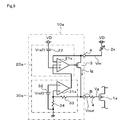
- FIG. 8 is a first electrical configuration diagram showing the sixth embodiment
- FIG. 9 is a second electrical configuration diagram showing the sixth embodiment
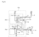
- FIG. 10 is a first electrical configuration diagram showing the seventh embodiment
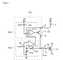
- FIG. 11 is a second electrical configuration diagram showing the seventh embodiment.
- a gate drive circuit 10 drives an IGBT 1 as a gate drive type switching element.
- the gate drive circuit 10 is supplied with power from the DC power supply VD through the shunt resistor 2 for current detection to the input terminal A, and drives the gate to the output terminal B via the source-drain of the P-channel MOSFET 3 as an output element. Output a signal.
- the output terminal B is connected to the gate of the IGBT 1 via the gate resistor 4.
- the gate drive circuit 10 includes a constant current drive circuit 20 and a constant voltage drive circuit 30.
- the constant current drive circuit 20 has a first differential amplifier 21 and a first reference power supply 22.
- the input voltage Vin is input from the DC power supply VD from the input terminal A via the shunt resistor 2 to the inverting input terminal of the first differential amplifier 21, and the non-inverting input terminal is input from the DC power supply VD via the first reference power supply 22.
- the first reference voltage Vref1 is input.
- the constant voltage drive circuit 30 includes a three-input type second differential amplifier 31, a second reference power source 32, and voltage dividing resistors 33 and 34.
- the voltage dividing resistors 33 and 34 form a voltage dividing circuit by being connected in series, and are connected between the output terminal B and the ground.
- the common connection point P of the voltage dividing resistors 33 and 34 outputs a voltage obtained by dividing the output voltage Vout of the output terminal B.
- the second reference voltage Vref2 of the second reference power supply 32 is input to the inverting input terminal of the second differential amplifier 31, and the output signal of the first differential amplifier 21 is input to the first non-inverting input terminal of the second differential amplifier 31.
- the divided voltage of the output voltage Vout is input to the non-inverting input terminal via the voltage dividing resistor 33.
- the second differential amplifier 31 calculates the difference between the second reference voltage Vref2 input to the inverting input terminal and the smaller value of the first and second non-inverting input terminals to obtain the difference value.
- the corresponding signal is output. That is, the second differential amplifier 31 corresponds to the difference between the output voltage of the first differential amplifier 21 and the divided voltage of the output voltage Vout, whichever is smaller, with the second reference voltage Vref2.
- the voltage is output to the gate of MOSFET3.
- the above configuration is a configuration for driving the IGBT 1 on, but the gate drive circuit 10 also includes a circuit configuration for off driving.
- an N-channel type MOSFET is connected between the gate of the IGBT 1 and the ground, is turned on after the MOSFET 3 is turned off, and is configured to discharge the gate charge of the IGBT 1 to turn it off.
- the gate drive circuit 10 having the above-described configuration applies a gate voltage to the IGBT 1 to be turned on when a high-level on-gate drive signal Sg is externally applied. Similarly, when the low-level gate drive signal Sg for instructing to turn off is applied, the gate drive circuit 10 stops applying the gate voltage to the IGBT 1 and discharges the gate charge to turn off the gate charge.
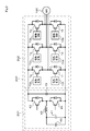
- FIG. 1 is a configuration including a motor generator 100 having both functions of a motor and a generator and a power conversion device 200.
- the motor generator 100 is used in an electric vehicle or the like.
- the power conversion device 200 has a function of generating a three-phase alternating current from the battery 40 to drive the motor/generator 100 to rotate, and a function of converting a power output of the motor/generator 100 into a direct current and charging the battery 40.
- the power conversion device 200 includes a DC power supply unit 201 and a three-phase inverter unit 202.
- a capacitor 41 is connected in parallel to the battery 40, which is a DC power supply.
- High voltage DC power is generated by energizing the booster coil 42 from the battery 40 by on/off control of the switching elements 43 and 44 to generate high voltage and charging the capacitor 45 connected to the output stage.
- the three-phase inverter unit 202 includes six IGBTs 1a to 1f and forms a three-phase inverter circuit. The outputs of the three-phase arms are connected to the three terminals of the motor generator 100.
- the six IGBTs 1a to 1f are drive-controlled by being supplied with gate voltages by similarly configured drive circuits 10a to 10f.
- Each of the drive circuits 10a to 10f has the same configuration as the gate drive circuit 10 shown in FIG.
- the DC power supply unit 201 when rotating the motor generator 100, controls the IGBTs 43 and 44 to be turned on and off, thereby boosting the terminal voltage of the battery 40 by the boosting coil 42 and causing the capacitor 45 to reach the capacitor 45.
- the capacitors 45 are used as a DC power source to drive the IGBTs 1a to 1f on and off by the drive circuits 10a to 10f, respectively, to generate a three-phase alternating current and supply power to the motor generator 100.
- the motor generator 100 functions as a generator
- three-phase alternating current generated by rotation is converted into direct current through the three-phase inverter circuit 202 and the capacitor 45 is charged.
- the electric charge of the capacitor 45 charges the battery 40 with the DC voltage reduced via the boosting coil 42 by turning on and off the IGBTs 43 and 44 in the DC power supply unit 201.
- the motor generator 100 is rotationally driven by supplying power to the battery 40 with the power converter 200 in a three-phase alternating current, and in the case of regenerating electric power as a generator, the power converter 200 performs DC conversion and step-down. Then, it can be returned to the battery 40.
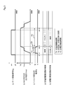
- the gate drive circuit 10 starts operating at time t1 when a high-level gate drive signal Sg for instructing to turn on is externally applied at time t0.
- the input voltage Vin is applied to the input terminal A from the DC power supply VD via the shunt resistor 2.
- the first differential amplifier 21 turns on the MOSFET 3 because a voltage higher than the voltage set by the reference voltage Vref1 is applied to the inverting input terminal.
- a voltage drop occurs due to the current Ig flowing from the DC power supply VD to the shunt resistor 2, and the input voltage Vin becomes lower than the terminal voltage of the DC power supply VD.
- the input voltage Vin becomes a voltage lowered by the voltage obtained by the product of the current Ig flowing from the DC power supply VD to the shunt resistor 2, if the resistance value of the shunt resistor 2 is Rs, the input voltage Vin will be The voltage drops from the voltage of VD by “Rs ⁇ Ig”, which is the voltage drop at the shunt resistor 2.
- the first differential amplifier 21 outputs a signal according to the difference between the input voltage Vin and the voltage set by the first reference voltage Vref1.
- the output of the first differential amplifier 21 is controlled so that a predetermined gate current Ig set by the first reference voltage Vref1 flows through the shunt resistor 2.
- the output signal of the first differential amplifier 21 is input to the second differential amplifier 31 of the constant voltage drive circuit 30.
- the output voltage Vout of the output terminal B is controlled to be the predetermined gate voltage Vg set by the second reference voltage Vref2. In this case, when the output voltage Vout of the output terminal B has not reached the predetermined gate voltage Vg, the voltage applied to the second non-inverting input terminal is low, so that the MOSFET 3 is fully turned on as shown in FIG. Try to.
- the second differential amplifier 31 since the value corresponding to the difference between the output signal from the first differential amplifier 21 and the second reference voltage Vref2 is smaller, as shown in FIG.
- the output signal from the first differential amplifier 21 becomes a dominant control element, and as a result, a gate signal for flowing a constant current is output to the gate of the MOSFET 3 in a controlled state.
- the MOSFET 3 is controlled so that the gate current Ig flows at a constant current as shown in FIG. 3C, and is output from the output terminal B to the gate of the IGBT 1.
- the constant current Ig flows through the gate and the gate capacitance is charged with the constant current, so that the gate voltage Vg rises at a constant voltage change rate, as shown in FIG. 3B.
- the gate voltage Vg is fixed to the mirror voltage Vmr until the time t2 when the mirror period ends.
- the period T1 from time t0 to t2 is a constant current drive period in which the control by the constant current drive circuit 20 is performed.
- the gate voltage Vg of the IGBT1 rises again at a constant voltage change rate.
- the gate current Ig of the MOSFET 3 decreases and the gate voltage Vg reaches the predetermined level at time t3.
- the period T2 from the time t2 to the time t3 is a constant current-constant voltage transition period in which the control state of constant current drive shifts to the control state of constant voltage drive.
- the constant current drive circuit 20 performs the constant current control, and the MOSFET 3 is in the state of being controlled by the constant current output.
- the first differential amplifier 21 of the constant current drive circuit 20 fully turns on the MOSFET 3 to flow the current.
- the second differential amplifier 31 since the output voltage Vout of the constant voltage drive circuit 30 has reached the predetermined gate voltage Vg, the second differential amplifier 31 has almost the same level as the second reference voltage Vref2. Therefore, the second differential amplifier 31 serves as an output for turning off the MOSFET 3.
- the second differential amplifier 31 stops the current output to the gate of the MOSFET 3 because the output voltage Vout reaches the predetermined voltage regardless of the signal output from the first differential amplifier 21. It becomes a state.
- the second differential amplifier 31 controls the MOSFET 3 according to the fluctuation, and causes a gate current to flow through the IGBT 1 to generate a gate voltage. The control state is maintained to hold Vg.
- the MOSFET 3 for giving the gate voltage of the IGBT 1 is driven by the gate drive circuit 10 immediately after being turned on by the constant current drive circuit 20 to perform constant current drive, and thereafter, when the gate voltage Vg reaches a predetermined level. Constant voltage driving is performed by the constant voltage driving circuit 30.
- the gate drive circuit 10 causes the off drive circuit to discharge the gate charge of the IGBT 1 at time t5, as shown in FIG.
- the gate voltage Vg is reduced to zero to turn off the IGBT 1.
- the period T3 from the time t3 to t5 is a constant voltage drive period in which the control by the constant voltage drive circuit 30 is performed.
- the MOSFET 3 is provided as a common output element, and the gate of the IGBT 1 can be driven by switching the control automatically by the constant current drive circuit 20 and the constant voltage drive circuit 30.
- the gate drive circuit 10 can be constructed at low cost.
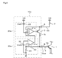
- FIG. 4 shows the second embodiment, and hereinafter, portions different from the first embodiment will be described.
- the gate drive circuit 10a includes a constant current drive circuit 20a and a constant voltage drive circuit 30a, and the constant current drive circuit 20a outputs a gate signal to the gate of the MOSFET 3.
- the constant current drive circuit 20a includes a first differential amplifier 21a instead of the first differential amplifier 21.
- the first differential amplifier 21a is of a 3-input type and has a function corresponding to the second differential amplifier 31 of the constant voltage drive circuit 30 in the first embodiment.
- the constant voltage drive circuit 30a includes a two-input second differential amplifier 31a instead of the second differential amplifier 31.
- the second embodiment employs a configuration in which the first differential amplifier 21 and the second differential amplifier 31 in the first embodiment are functionally replaced.
- the first differential amplifier 21a receives the input voltage Vin from the DC power supply VD via the shunt resistor 2 and the input terminal A to the first inverting input terminal.
- the output signal of the second differential amplifier 31a is input to the second inverting input terminal of the first differential amplifier 21a, and the first reference voltage is supplied from the DC power supply VD to the non-inverting input terminal via the first reference power supply 22.
- Vref1 is input.
- the output terminal of the first differential amplifier 21a is connected to the gate of the MOSFET 3 and applies a gate voltage.
- the second differential amplifier 31a receives the second reference voltage Vref2 of the second reference power supply 32 at its inverting input terminal and outputs it at its non-inverting input terminal via the voltage dividing resistor 33.
- the divided voltage of the voltage Vout is input.
- the first differential amplifier 21a corresponds to a voltage value having a smaller difference between the first reference voltage Vref1 input to the non-inverting input terminal and the values of the first and second inverting input terminals.
- the voltage corresponding to the difference from the 1 reference voltage Vref1 is output to the gate of the MOSFET 3.
- the first differential amplifier 21a generates a gate drive signal for the MOSFET 3 similarly to the second differential amplifier 31 of the first embodiment. Therefore, the gate drive circuit 10a performs the constant current drive by the control of the constant current drive circuit 20a immediately after the IGBT 1 is turned on, and when the gate voltage Vg reaches a predetermined level thereafter, the constant voltage drive circuit 30a performs the constant voltage drive. Will be implemented. As a result, according to the second embodiment as described above, it is possible to obtain the same effect as that of the first embodiment.
- FIG. 5 shows the third embodiment, and the portions different from the first embodiment will be described below.
- the MOSFET 3 has a source directly connected to the DC power supply VD via the input terminal A and a drain connected to the output terminal B via the shunt resistor 2.
- the gate drive circuit 10b is based on the gate drive circuit 10 in the first embodiment, and the constant voltage drive circuit 30b has the same configuration as the constant voltage drive circuit 30.
- both terminals of the shunt resistor 2 are connected between both terminals of the first differential amplifier 21, and the terminal voltage of the shunt resistor 2 is input.
- a voltage proportional to the current Ig flowing through the shunt resistor 2 is generated as in the first embodiment.
- the constant current drive circuit 20b outputs a gate drive signal such that the first differential amplifier 21 causes a constant current Ig set by the second reference voltage Vref2 to flow to the gate of the MOSFET 3.
- the constant current drive circuit 20b since the output voltage Vout of the output terminal B has not reached the predetermined voltage, the input signal to the second differential amplifier 31 becomes small, so that the difference from the second reference voltage Vref2 is small. growing. On the other hand, the difference between the output signal from the first differential amplifier 21 of the constant current drive circuit 20b and the second reference voltage Vref2 becomes small. As a result, in this state, the constant current drive circuit 20b enters the constant current control state.
- FIG. 6 shows the fourth embodiment. Hereinafter, parts different from the third embodiment will be described.
- the shunt resistor 2 of the third embodiment is omitted, and the gate resistance Ig is detected by the gate resistor 4.
- the gate drive signal can be output to the MOSFET 3 as in the third embodiment, the drive control of the IGBT 1 can be performed in the same manner, and the same effect can be obtained.
- the gate resistance 4 is used for current detection, the number of resistance elements can be reduced when the functions of the gate current detection operation and the gate input resistance can be combined.
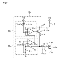
- FIG. 7 shows the fifth embodiment, and hereinafter, parts different from the second embodiment will be described.
- the gate drive circuit 10a has the same configuration as that of the second embodiment.
- an n-channel MOSFET 1a is driven instead of the IGBT 1.
- the MOSFET 1a is controlled by the constant voltage drive circuit 20a for constant current drive at the time of on-driving similarly to the second embodiment, and is controlled by the constant voltage drive circuit 30a when the gate voltage reaches a predetermined level. Drive control is performed. Therefore, also in the fifth embodiment, it is possible to obtain the same effects as those in the second embodiment.
- FIG. 8 and FIG. 9 show the sixth embodiment, and only portions different from the fifth embodiment will be described below.
- the sixth embodiment employs a configuration in which the value of the constant current Ig can be changed in the constant current drive control of FIGS. 8 and 9.
- the gate drive circuit 10x of the fifth embodiment is provided with a constant current drive circuit 20x instead of the constant current drive circuit 20a.
- a variable first reference power supply 22x that supplies a variable first reference voltage Vref1x is provided instead of the first reference power supply 22 that supplies the first reference voltage Vref1.
- the level when the constant current Ig flows in the gate of the MOSFET 3 can be set to different levels by adjusting the variable first reference voltage Vref1x. This makes it possible to adjust the voltage change rate when raising the gate voltage Vg of the MOSFET 1a.
- the gate drive circuit 10a is the same as that of the fifth embodiment, and instead of the shunt resistor 2 having a predetermined shunt resistor R, a variable shunt resistor 2x capable of setting the variable shunt resistor Rx is provided. It is configured. As a result, even if the current Ig is the same, the value of the variable shunt resistor Rx of the variable shunt resistor 2x is changed, so that the input voltage Vin of the input terminal A is changed. Therefore, the level of the constant current set by the first reference voltage Vref1 is set to a substantially different level. This makes it possible to adjust the voltage change rate when raising the gate voltage Vg of the MOSFET 1a.
- variable first reference voltage Vref1x is adjusted by the variable first reference power supply 22x, or the resistance value of the variable shunt resistance value Rx is adjusted by the variable shunt resistor 2x.
- the level of the current Ig can be set to different levels. As a result, it is possible to cope with variations in the characteristics of the MOSFET 3 and the characteristics of the MOSFET 1a to be controlled, and to easily perform drive control under different conditions.
- FIG. 10 and FIG. 11 show the seventh embodiment, and the portions different from the fifth embodiment will be described below.
- the seventh embodiment employs a configuration in which the value of the constant voltage Vg can be changed in the constant voltage drive control of FIGS. 10 and 11.
- the gate drive circuit 10a of the fifth embodiment has a gate drive circuit 10y provided with a constant voltage drive circuit 30y instead of the constant voltage drive circuit 30a.
- a variable second reference power supply 32y that supplies a variable second reference voltage Vref2y is provided instead of the second reference power supply 32 that supplies the second reference voltage Vref2.
- the level when the constant voltage Vg is applied to the gate of the MOSFET 3 can be set to a different level by adjusting the variable second reference voltage Vref2y. This makes it possible to adjust to which level the gate voltage Vg of the MOSFET 1a is set.
- a constant voltage drive circuit 30z is provided instead of the constant voltage drive circuit 30a.
- variable voltage dividing resistors 33z and 34z are provided instead of the voltage dividing resistors 33 and 34 that detect the output voltage Vout.
- the constant voltage drive circuit 30z can adjust the level when the constant voltage Vg is applied to the gate of the MOSFET 3 and the voltage level for detecting the output voltage Vout of the output terminal B. This makes it possible to adjust to which level the gate voltage Vg of the MOSFET 1a is set.
- the detection level of the output voltage Vout is adjusted by adjusting the variable second reference voltage Vref2y with the variable second reference power supply 32y or adjusting the resistance values of the variable voltage dividing resistors 33z and 34z. Can be set to different levels. As a result, it is possible to cope with variations in the characteristics of the MOSFET 3 and the characteristics of the MOSFET 1a to be controlled, and to easily perform drive control under different conditions.
- control target can be the MOSFET 1a instead of the IGBT 1.
- controlled object can be the IGBT 1 instead of the MOSFET 1a.
- the level setting change of the variable first reference voltage Vref1x or the variable second reference voltage Vref2y, and the setting change of the resistance value of the variable shunt resistor 2x or the variable voltage dividing resistors 33z, 34z A configuration that can be set manually or electrically can be adopted. Further, in the configuration of electrically setting, a circuit for automatically adjusting to achieve a predetermined control level can be separately provided.
- the first to seventh embodiments can form a composite gate drive circuit that is appropriately combined with each other.
- the gate drive circuits 10, 10a, 10b, 10c, 10x, 10y, 10z of the present embodiment are also applied to gate drive type switching elements in circuit configurations other than the IGBTs 1a to 1f of the three-phase inverter 202 that drives the motor generator 100. can do.
Landscapes
- Engineering & Computer Science (AREA)
- Power Engineering (AREA)
- Power Conversion In General (AREA)
- Electronic Switches (AREA)
Abstract
ゲート駆動形スイッチング素子(1、1a)のゲートにゲート駆動信号を与える出力素子(3)と、前記ゲート駆動形スイッチング素子のゲートに前記ゲート駆動信号を定電流で与えるように前記出力素子を制御する定電流駆動回路(20、20a、20b、20c、20x)と、前記ゲート駆動形スイッチング素子のゲートに前記ゲート駆動信号を定電圧で与えるように前記出力素子を制御する定電圧駆動回路(30、30a、30b、30c、30y、30z)とを備えたゲート駆動回路。
Description
本開示は、2018年12月10日に出願された日本出願番号2018-230804号に基づくもので、ここにその記載内容を援用する。
本開示は、ゲート駆動回路に関する。
IGBT(Insulated Gate Bipolar Transistor)やパワーMOSFETなどのゲート駆動形スイッチング素子は、短絡等が発生して過電流が流れる場合に、その過電流が流れ続けるとスイッチング素子自身に急激な温度上昇が発生して破壊に至ることがある。スイッチング素子の短絡で過電流が流れるときに発生する短絡エネルギーは、例えばIGBTではゲート-エミッタ間に発生しているゲート電圧が高いほど大きくなる。このため、スイッチング素子を駆動するゲート駆動回路においては、短絡エネルギーを低減して破壊を防止することを目的として、オン駆動時にゲート電圧を一定に制御することが求められる。
このようなスイッチング素子を駆動するゲート駆動回路としては、定電圧制御型のものや定電流制御型のものがある。この場合、定電圧制御型のものは、定電圧制御回路のみでゲート電圧を一定に制御しながらスイッチングオン駆動可能である。このため定電圧制御型のものは、定電流駆動型よりも素子点数を少なくできるためコストを抑えられるメリットがあるが、スイッチング損失が大きいという課題がある。
一方、定電流制御型のものは、定電圧駆動型よりもスイッチング損失が小さいというメリットがあるが、上流に電源回路を設ける必要があり、一般的には複数の出力パワー素子を直列に接続する必要があるため、コストが高くなるという課題がある。
本開示は、定電圧および定電流の2つの制御機能を備え、且つ駆動部の出力素子を増設することがなく、低コストな構成のゲート駆動回路を提供することを目的とする。
請求項1に記載のゲート駆動回路は、ゲート駆動形スイッチング素子のゲートにゲート駆動信号を与える出力素子と、前記ゲート駆動形スイッチング素子のゲートに前記ゲート駆動信号を定電流で与えるように前記出力素子を制御する定電流駆動回路と、前記ゲート駆動形スイッチング素子のゲートに前記ゲート駆動信号を定電圧で与えるように前記出力素子を制御する定電圧駆動回路とを備えている。
上記構成を採用することにより、ゲート駆動形スイッチング素子のゲートに対して、出力素子によりゲート駆動信号を与える構成で、定電流駆動回路はゲート駆動信号を定電流で与えるように制御し、定電圧駆動回路はゲート駆動信号を定電圧で与えるように制御する。これにより、ゲート駆動形スイッチング素子は、ゲート電圧が定電流により一定の電圧上昇率で上昇し、この後所定のゲート電圧に達すると、定電圧を保持するように制御される。そして、この場合に、定電流制御および定電圧制御のいずれも一つの出力素子を介して実施することができ、低コストで構成することができる。
本開示についての上記目的およびその他の目的、特徴や利点は、添付の図面を参照しながら下記の詳細な記述により、より明確になる。その図面は、
図1は、第1実施形態を示す電気的構成図であり、
図2は、第1実施形態を示す適用装置の全体の電気的構成図であり、
図3は、第1実施形態を示すタイムチャートであり、
図4は、第2実施形態を示す電気的構成図であり、
図5は、第3実施形態を示す電気的構成図であり、
図6は、第4実施形態を示す電気的構成図であり、
図7は、第5実施形態を示す電気的構成図であり、
図8は、第6実施形態を示す電気的構成図その1であり、
図9は、第6実施形態を示す電気的構成図その2であり、
図10は、第7実施形態を示す電気的構成図その1であり、
図11は、第7実施形態を示す電気的構成図その2である。
(第1実施形態)
以下、第1実施形態について、図1~図3を参照して説明する。
電気的構成を示す図1において、ゲート駆動回路10は、ゲート駆動形スイッチング素子としてのIGBT1を駆動するものである。ゲート駆動回路10は、入力端子Aに直流電源VDから電流検出用のシャント抵抗2を介して給電され、出力素子としてのPチャンネル型のMOSFET3のソース-ドレイン間を介して出力端子Bにゲート駆動信号を出力する。出力端子Bはゲート抵抗4を介してIGBT1のゲートに接続される。
以下、第1実施形態について、図1~図3を参照して説明する。
電気的構成を示す図1において、ゲート駆動回路10は、ゲート駆動形スイッチング素子としてのIGBT1を駆動するものである。ゲート駆動回路10は、入力端子Aに直流電源VDから電流検出用のシャント抵抗2を介して給電され、出力素子としてのPチャンネル型のMOSFET3のソース-ドレイン間を介して出力端子Bにゲート駆動信号を出力する。出力端子Bはゲート抵抗4を介してIGBT1のゲートに接続される。
ゲート駆動回路10は、定電流駆動回路20および定電圧駆動回路30を備えている。定電流駆動回路20は、第1差動アンプ21および第1参照電源22を有する。第1差動アンプ21の反転入力端子には入力端子Aからシャント抵抗2を介して直流電源VDから入力電圧Vinが入力され、非反転入力端子には直流電源VDから第1参照電源22を介して第1参照電圧Vref1が入力される。
定電圧駆動回路30は、3入力型の第2差動アンプ31、第2参照電源32および分圧抵抗33、34を備えている。分圧抵抗33および34は直列接続することで分圧回路を構成し、出力端子Bとグランドとの間に接続される。分圧抵抗33および34の共通接続点Pは、出力端子Bの出力電圧Voutを分圧した電圧を出力する。第2差動アンプ31の反転入力端子には第2参照電源32の第2参照電圧Vref2が入力され、第1非反転入力端子には第1差動アンプ21の出力信号が入力され、第2非反転入力端子には分圧抵抗33を介して出力電圧Voutの分圧電圧が入力される。
第2差動アンプ31は、反転入力端子に入力されている第2参照電圧Vref2に対して、第1および第2非反転入力端子のいずれか小さい値との差を演算して差の値に応じた信号を出力する。つまり、第2差動アンプ31は、第1差動アンプ21の出力電圧および出力電圧Voutの分圧電圧のいずれか小さい方の電圧値に対して、第2参照電圧Vref2との差に相当する電圧をMOSFET3のゲートに出力する。
なお、上記構成はIGBT1をオン駆動するための構成であるが、ゲート駆動回路10としては、オフ駆動をするための回路構成も備えている。例えばNチャンネル型のMOSFETが、IGBT1のゲートとグランドとの間に接続され、MOSFET3がオフされた後にオン駆動され、IGBT1のゲート電荷を放電させてオフ動作させるように構成されている。
また、上記構成のゲート駆動回路10は、外部からハイレベルであるオンのゲート駆動信号Sgが与えられると、IGBT1にゲート電圧を印加してオン動作させる。同様に、ゲート駆動回路10は、オフ指示のローレベルのゲート駆動信号Sgが与えられると、IGBT1へのゲート電圧印加を停止すると共に、ゲート電荷を放電させてオフ動作させる。
次に、上記構成を採用したゲート駆動回路10の使用形態の一例となる電気的構成を図2により説明する。モータと発電機との機能を兼ね備えた電動発電機100と電力変換装置200からなる構成である。電動発電機100は、電気自動車などで用いられるものである。電力変換装置200は、バッテリ40から三相交流を生成して電動発電機100を回転駆動すると共に、電動発電機100による発電出力を直流に変換してバッテリ40に充電する機能を有する。
電力変換装置200は、直流電源部201および三相インバータ部202を備える。直流電源部201において、直流電源であるバッテリ40にはコンデンサ41が並列に接続されている。バッテリ40から昇圧コイル42にスイッチング素子43および44のオンオフ制御により通電して高圧を発生させ、出力段に接続されたコンデンサ45に充電することで高電圧直流電源を生成する。
三相インバータ部202は、6個のIGBT1a~1fを備え、三相のインバータ回路を形成している。三相の各アームの出力が電動発電機100の3つの各端子に接続される。6個のIGBT1a~1fは、同様に構成された駆動回路10a~10fによりゲート電圧が与えられて駆動制御される。駆動回路10a~10fは、いずれも図1に示したゲート駆動回路10と同等の構成である。
次に、上記構成の電力変換装置200の動作について簡単に説明をし、その後、ゲート駆動回路10の動作について、図3のタイムチャートも参照して説明する。
電力変換装置200において、直流電源部201は、電動発電機100を回転駆動させる場合には、IGBT43および44をオンオフ制御することにより、バッテリ40の端子電圧を昇圧コイル42により昇圧させてコンデンサ45に充電する。三相インバータ202では、コンデンサ45を直流電源としてIGBT1a~1fをそれぞれの駆動回路10a~10fによりオンオフ駆動され、三相交流を生成して電動発電機100に給電する。
電力変換装置200において、直流電源部201は、電動発電機100を回転駆動させる場合には、IGBT43および44をオンオフ制御することにより、バッテリ40の端子電圧を昇圧コイル42により昇圧させてコンデンサ45に充電する。三相インバータ202では、コンデンサ45を直流電源としてIGBT1a~1fをそれぞれの駆動回路10a~10fによりオンオフ駆動され、三相交流を生成して電動発電機100に給電する。
一方、電動発電機100が発電機として機能する場合には、回転により生ずる三相交流を、三相インバータ回路202を介して直流に変換してコンデンサ45に充電する。コンデンサ45の電荷は、直流電源部201においてIGBT43および44をオンオフ駆動させることで昇圧コイル42を介して降圧した直流電圧でバッテリ40に充電する。
これにより、電動発電機100は、電力変換装置200によりバッテリ40の電源を三相交流にして給電して回転駆動され、発電機として電力を回生する場合には電力変換装置200により直流変換および降圧してバッテリ40に戻すことができる。
次に、ゲート駆動回路10の作用について説明する。ゲート駆動回路10は、図3(a)に示すように、時刻t0で外部からオン指示のハイレベルのゲート駆動信号Sgが与えられると、時刻t1から動作を開始する。まず、定電流駆動回路20においては、直流電源VDからシャント抵抗2を介して入力端子Aに入力電圧Vinとして与えられる。これにより、第1差動アンプ21は参照電圧Vref1で設定された電圧よりも高い電圧が反転入力端子に与えられるので、MOSFET3をオンさせる。このとき、直流電源VDからシャント抵抗2に流れる電流Igにより電圧降下が生じて入力電圧Vinは直流電源VDの端子電圧よりも下がる。
入力電圧Vinは、直流電源VDからシャント抵抗2に流れる電流Igとの積で得られる電圧分だけ下がった電圧となるから、シャント抵抗2の抵抗値をRsとすると、入力電圧Vinは、直流電源VDの電圧からシャント抵抗2での電圧降下分である「Rs×Ig」だけ下がった電圧となる。
第1差動アンプ21は、入力電圧Vinと第1参照電圧Vref1で設定される電圧との差分に応じた信号を出力する。第1差動アンプ21の出力は、シャント抵抗2に第1参照電圧Vref1で設定された所定のゲート電流Igが流れるように制御する。この第1差動アンプ21の出力信号は、定電圧駆動回路30の第2差動アンプ31に入力される。
定電圧駆動回路30においては、出力端子Bの出力電圧Voutが、第2参照電圧Vref2で設定される所定のゲート電圧Vgとなるように制御する。この場合、出力端子Bの出力電圧Voutが所定のゲート電圧Vgに達していない状態では、第2非反転入力端子に与える電圧が低いので、図3(e)に示すように、MOSFET3をフルオンさせようとする。
しかし、第2差動アンプ31においては、第1差動アンプ21からの出力信号と第2参照電圧Vref2との差分に相当する値の方が小さいので、図3(d)に示すように、第1差動アンプ21からの出力信号が支配的な制御要素となり、結果として定電流を流すためのゲート信号がMOSFET3のゲートに出力される制御状態となる。
これにより、MOSFET3は、図3(c)に示すように、ゲート電流Igが定電流で流れるように制御され、出力端子BからIGBT1のゲートに出力される。IGBT1は、ゲートに定電流Igが流れてゲート容量に定電流で充電されることで、図3(b)に示すように、ゲート電圧Vgは一定の電圧変化率で上昇する。なお、途中IGBT1のゲート電圧が一定となるミラー期間に入ると、ミラー期間が終了する時刻t2までの期間中、ゲート電圧Vgはミラー電圧Vmrに固定される。この結果、時刻t0からt2までの期間T1は定電流駆動回路20による制御が実施される定電流駆動期間となる。
時刻t2になってミラー期間が終了すると、IGBT1のゲート電圧Vgは再び一定の電圧変化率で上昇してゆく。この後、IGBT1のゲートへの充電が進んでゲート電圧Vgが所定レベルに近づくと、MOSFET3のゲート電流Igは低下してゆき、時刻t3でゲート電圧Vgが所定レベルに達する。この結果、時刻t2からt3までの期間T2は、定電流駆動の制御状態から定電圧駆動の制御状態に移行する定電流-定電圧移行期間となる。また、期間T1およびT2の期間中は、定電流駆動回路20により定電流制御が行われ、MOSFET3が定電流出力で制御される状態である。
そして、時刻t3以降の状態では、電流Igがほとんどゼロになるので、図3(d)に示すように、定電流駆動回路20の第1差動アンプ21はMOSFET3をフルオンさせて電流を流そうとする。一方、定電圧駆動回路30の出力電圧Voutが所定のゲート電圧Vgに達したことで、第2差動アンプ31においては、第2参照電圧Vref2とほぼ同じレベルになる。このため、第2差動アンプ31は、MOSFET3をオフさせる出力となる。
つまり、時刻t3以降においては、第2差動アンプ31は、第1差動アンプ21からの信号出力にかかわらず、出力電圧Voutが所定電圧に達したことでMOSFET3のゲートに対する電流出力を停止する状態となる。これにより、第2差動アンプ31は、以後、図3(e)に示すように、IGBT1のゲート電圧Vgが変動すると、これに応じてMOSFET3を制御してIGBT1にゲート電流を流してゲート電圧Vgを保持する制御状態となる。
このようにして、IGBT1のゲート電圧を与えるMOSFET3は、ゲート駆動回路10により、オンした直後は定電流駆動回路20の制御により定電流駆動を実施し、この後ゲート電圧Vgが所定レベルに達すると定電圧駆動回路30により定電圧駆動が実施されるようになる。
なお、この後、時刻t4でローレベルのゲート駆動信号Sgが与えられると、ゲート駆動回路10は、時刻t5でオフ駆動回路によりIGBT1のゲート電荷を放電させて図3(b)示のようにゲート電圧Vgをゼロまで低下させて、IGBT1をオフ動作させる。この結果、時刻t3からt5までの期間T3は、定電圧駆動回路30による制御が実施される定電圧駆動期間となる。
このような第1実施形態によれば、共通の出力素子としてMOSFET3を設けて、IGBT1のゲートを定電流駆動回路20および定電圧駆動回路30により自動的に制御を切り替えて駆動することができるので、低コストでゲート駆動回路10を構成することができる。
(第2実施形態)
図4は第2実施形態を示すもので、以下、第1実施形態と異なる部分について説明する。この実施形態では、ゲート駆動回路10aは、定電流駆動回路20aおよび定電圧駆動回路30aを備え、MOSFET3のゲートに対して定電流駆動回路20aによりゲート信号を出力する構成である。
図4は第2実施形態を示すもので、以下、第1実施形態と異なる部分について説明する。この実施形態では、ゲート駆動回路10aは、定電流駆動回路20aおよび定電圧駆動回路30aを備え、MOSFET3のゲートに対して定電流駆動回路20aによりゲート信号を出力する構成である。
定電流駆動回路20aは、第1差動アンプ21に代えて第1差動アンプ21aを備える。第1差動アンプ21aは、3入力型のもので、第1実施形態における定電圧駆動回路30の第2差動アンプ31に相当する機能を備える。一方、定電圧駆動回路30aは、第2差動アンプ31に代えて2入力の第2差動アンプ31aを備える。この第2実施形態では、第1実施形態における第1差動アンプ21と第2差動アンプ31とを機能的に入れ替えた構成を採用している。
定電流駆動回路20aにおいては、第1差動アンプ21aは、第1反転入力端子に直流電源VDからシャント抵抗2および入力端子Aを介して入力電圧Vinが入力される。また、第1差動アンプ21aは、第2反転入力端子に第2差動アンプ31aの出力信号が入力され、非反転入力端子に直流電源VDから第1参照電源22を介して第1参照電圧Vref1が入力される。第1差動アンプ21aの出力端子はMOSFET3のゲートに接続され、ゲート電圧を印加する。
また、定電圧駆動回路30aにおいては、第2差動アンプ31aは、反転入力端子に第2参照電源32の第2参照電圧Vref2が入力され、非反転入力端子に分圧抵抗33を介して出力電圧Voutの分圧電圧が入力される。
第1差動アンプ21aは、非反転入力端子に入力されている第1参照電圧Vref1に対して、第1および第2反転入力端子の値との差が小さい方の電圧値に対応して第1参照電圧Vref1との差に相当する電圧をMOSFET3のゲートに出力する。
これにより、第1差動アンプ21aは、第1実施形態の第2差動アンプ31と同様にしてMOSFET3に対してゲート駆動信号を生成するようになる。したがって、ゲート駆動回路10aは、IGBT1がオンした直後は定電流駆動回路20aの制御により定電流駆動を実施し、この後ゲート電圧Vgが所定レベルに達すると定電圧駆動回路30aにより定電圧駆動が実施されるようになる。
この結果、このような第2実施形態によっても第1実施形態と同様の作用効果を得ることができる。
この結果、このような第2実施形態によっても第1実施形態と同様の作用効果を得ることができる。
(第3実施形態)
図5は第3実施形態を示すもので、以下、第1実施形態と異なる部分について説明する。この実施形態では、MOSFET3は、ソースが入力端子Aを介して直流電源VDに直接接続され、ドレインはシャント抵抗2を介して出力端子Bに接続されている。
図5は第3実施形態を示すもので、以下、第1実施形態と異なる部分について説明する。この実施形態では、MOSFET3は、ソースが入力端子Aを介して直流電源VDに直接接続され、ドレインはシャント抵抗2を介して出力端子Bに接続されている。
ゲート駆動回路10bは、第1実施形態におけるゲート駆動回路10を前提とし、定電圧駆動回路30bは、定電圧駆動回路30と同等の構成としている。定電流駆動回路20bは、第1差動アンプ21の両端子間にシャント抵抗2の両端子が接続され、シャント抵抗2の端子間電圧が入力される。
上記構成によれば、第1実施形態と同様にしてシャント抵抗2に流れる電流Igに比例した電圧が発生する。定電流駆動回路20bは、第1差動アンプ21によりMOSFET3のゲートに対して第2参照電圧Vref2で設定された定電流Igが流れるようにゲート駆動信号を出力する。
このとき、定電圧駆動回路30bは、出力端子Bの出力電圧Voutが所定電圧に達していないことで第2差動アンプ31への入力信号は小さくなるので、第2参照電圧Vref2との差が大きくなる。一方、定電流駆動回路20bの第1差動アンプ21からの出力信号と第2参照電圧Vref2との差は小さくなる。この結果、この状態では、定電流駆動回路20bによる定電流制御状態となる。
MOSFET3のゲート電圧Voutが、ミラー期間を過ぎて所定のゲート電圧Vgに達すると、出力端子Bから定電圧駆動回路30bの第2差動アンプ31への信号が大きくなり、第2参照電圧Vref2との差が小さくなる。一方、これによってゲート電流Igがほぼゼロになるので、第1差動アンプ21からの出力信号は大きくなる。この結果、この状態では定電圧駆動回路30bによる定電圧制御状態となる。
したがって、このような第3実施形態によっても第1実施形態と同様の作用効果をえることができる。
したがって、このような第3実施形態によっても第1実施形態と同様の作用効果をえることができる。
(第4実施形態)
図6は第4実施形態を示すもので、以下、第3実施形態と異なる部分について説明する。この実施形態では、第3実施形態のシャント抵抗2を省略し、ゲート電流Igの検出をゲート抵抗4により行う構成としている。
図6は第4実施形態を示すもので、以下、第3実施形態と異なる部分について説明する。この実施形態では、第3実施形態のシャント抵抗2を省略し、ゲート電流Igの検出をゲート抵抗4により行う構成としている。
この構成によっても、第3実施形態と同様にしてMOSFET3にゲート駆動信号を出力することができ、同様にしてIGBT1の駆動制御を行うことができ、同様の効果を得ることができる。
また、この構成では、ゲート抵抗4を電流検出に用いるので、ゲート電流検出動作とゲート入力抵抗との機能を兼ね備えることができる場合には、抵抗素子の個数を減らすことができる。
(第5実施形態)
図7は第5実施形態を示すもので、以下、第2実施形態と異なる部分について説明する。この実施形態では、ゲート駆動回路10aは、第2実施形態と同様の構成を採用している。また、制御対象となるゲート駆動形スイッチング素子としてIGBT1に代えてnチャンネル型のMOSFET1aを駆動する構成である。
図7は第5実施形態を示すもので、以下、第2実施形態と異なる部分について説明する。この実施形態では、ゲート駆動回路10aは、第2実施形態と同様の構成を採用している。また、制御対象となるゲート駆動形スイッチング素子としてIGBT1に代えてnチャンネル型のMOSFET1aを駆動する構成である。
上記構成によれば、MOSFET1aは、第2実施形態と同様にして、オン駆動時にははじめに定電圧駆動回路20aにより定電流駆動制御され、ゲート電圧が所定レベルに達すると定電圧駆動回路30aにより定電圧駆動制御がなされる。
したがって、このような第5実施形態によっても、第2実施形態と同様の作用効果を得ることができる。
したがって、このような第5実施形態によっても、第2実施形態と同様の作用効果を得ることができる。
(第6実施形態)
図8および図9は第6実施形態を示すもので、以下、第5実施形態と異なる部分について説明する。第6実施形態においては、図8および図9のそれぞれの定電流駆動制御において、定電流Igの値を設定変更することができる構成を採用している。
図8および図9は第6実施形態を示すもので、以下、第5実施形態と異なる部分について説明する。第6実施形態においては、図8および図9のそれぞれの定電流駆動制御において、定電流Igの値を設定変更することができる構成を採用している。
図8に示すものでは、第5実施形態のゲート駆動回路10aにおいて、定電流駆動回路20aに代えて定電流駆動回路20xを設けたゲート駆動回路10xとしている。定電流駆動回路20xにおいては、第1参照電圧Vref1を与える第1参照電源22に代えて、可変第1参照電圧Vref1xを与える可変第1参照電源22xを設けている。
この構成を採用することにより、定電流駆動回路20xでは、MOSFET3のゲートに定電流Igを流す場合のレベルを、可変第1参照電圧Vref1xを調整することで異なるレベルに設定することができる。これによって、MOSFET1aのゲート電圧Vgを上昇させる場合の電圧変化率を調整することができる。
また、図9に示すものでは、ゲート駆動回路10aは第5実施形態のままとし、所定のシャント抵抗Rを有するシャント抵抗2に代えて、可変シャント抵抗Rxを設定可能な可変シャント抵抗2xを設ける構成としている。これにより、電流Igが同じでも可変シャント抵抗2xの可変シャント抵抗Rxの値が変更されることで入力端子Aの入力電圧Vinが変化する。このため、第1参照電圧Vref1で設定された定電流のレベルが実質的に異なるレベルに設定されたこととなる。これによって、MOSFET1aのゲート電圧Vgを上昇させる場合の電圧変化率を調整することができる。
このような第6実施形態によれば、可変第1参照電圧Vref1xを可変第1参照電源22xで調整したり、あるいは可変シャント抵抗2xにより可変シャント抵抗値Rxの抵抗値を調整することで、定電流Igのレベルを異なるレベルに設定することができる。これにより、MOSFET3の特性や制御対象となるMOSFET1aの特性のばらつきに対応したり、異なる条件での駆動制御を簡単に実施することができる。
(第7実施形態)
図10および図11は第7実施形態を示すもので、以下、第5実施形態と異なる部分について説明する。第7実施形態においては、図10および図11のそれぞれの定電圧駆動制御において、定電圧Vgの値を設定変更することができる構成を採用している。
図10および図11は第7実施形態を示すもので、以下、第5実施形態と異なる部分について説明する。第7実施形態においては、図10および図11のそれぞれの定電圧駆動制御において、定電圧Vgの値を設定変更することができる構成を採用している。
図10に示すものでは、第5実施形態のゲート駆動回路10aにおいて、定電圧駆動回路30aに代えて、定電圧駆動回路30yを設けたゲート駆動回路10yとしている。定電圧駆動回路30yにおいては、第2参照電圧Vref2を与える第2参照電源32に代えて、可変第2参照電圧Vref2yを与える可変第2参照電源32yを設けている。
この構成を採用することにより、定電圧駆動回路30yでは、MOSFET3のゲートに定電圧Vgを与える場合のレベルを、可変第2参照電圧Vref2yを調整することで異なるレベルに設定することができる。これによって、MOSFET1aのゲート電圧Vgをどのレベルに設定するかを調整することができる。
また、図11に示すものでは、第5実施形態のゲート駆動回路10aにおいて、定電圧駆動回路30aに代えて、定電圧駆動回路30zを設けたゲート駆動回路10zとしている。定電圧駆動回路30zにおいては、出力電圧Voutを検出する分圧抵抗33および34に代えて、可変分圧抵抗33zおよび34zを設ける構成としている。
この構成を採用することにより、定電圧駆動回路30zでは、MOSFET3のゲートに定電圧Vgを与える場合のレベルを、出力端子Bの出力電圧Voutを検出する電圧レベルを調整可能としている。これによって、MOSFET1aのゲート電圧Vgをどのレベルに設定するかを調整することができる。
このような第7実施形態によれば、可変第2参照電圧Vref2yを可変第2参照電源32yで調整したり、可変分圧抵抗33zおよび34zの抵抗値を調整することで出力電圧Voutの検出レベルを異なるレベルに設定することができる。これにより、MOSFET3の特性や制御対象となるMOSFET1aの特性のばらつきに対応したり、異なる条件での駆動制御を簡単に実施することができる。
(他の実施形態)
なお、本開示は、上述した実施形態のみに限定されるものではなく、その要旨を逸脱しない範囲で種々の実施形態に適用可能であり、例えば、以下のように変形または拡張することができる。
なお、本開示は、上述した実施形態のみに限定されるものではなく、その要旨を逸脱しない範囲で種々の実施形態に適用可能であり、例えば、以下のように変形または拡張することができる。
第1、第3、第4実施形態において、IGBT1に代えて制御対象をMOSFET1aとすることができる。第5~第7実施形態において、MOSFET1aに代えて制御対象をIGBT1とすることができる。
第6実施形態および第7実施形態では、可変第1参照電圧Vref1xあるいは可変第2参照電圧Vref2yのレベル設定変更や、可変シャント抵抗2xあるいは可変分圧抵抗33z、34zの抵抗値の設定変更について、手動によりあるいは電気的に設定可能な構成とすることもできる。また電気的に設定する構成では、所定の制御レベルを達成させるための自動調整する回路を別途設けることもできる。
第1~第7実施形態は、互いに適宜組み合わせた複合的なゲート駆動回路を構成することができる。
第1~第7実施形態は、互いに適宜組み合わせた複合的なゲート駆動回路を構成することができる。
本実施形態のゲート駆動回路10、10a、10b、10c、10x、10y、10zは、電動発電機100を駆動する三相インバータ202のIGBT1a~1f以外の回路構成におけるゲート駆動形スイッチング素子にも適用することができる。
本開示は、実施例に準拠して記述されたが、本開示は当該実施例や構造に限定されるものではないと理解される。本開示は、様々な変形例や均等範囲内の変形をも包含する。加えて、様々な組み合わせや形態、さらには、それらに一要素のみ、それ以上、あるいはそれ以下、を含む他の組み合わせや形態をも、本開示の範疇や思想範囲に入るものである。
Claims (6)
- ゲート駆動形スイッチング素子(1、1a)のゲートにゲート駆動信号を与える出力素子(3)と、
前記ゲート駆動形スイッチング素子のゲートに前記ゲート駆動信号を定電流で与えるように前記出力素子を制御する定電流駆動回路(20、20a、20b、20c、20x)と、
前記ゲート駆動形スイッチング素子のゲートに前記ゲート駆動信号を定電圧で与えるように前記出力素子を制御する定電圧駆動回路(30、30a、30b、30c、30y、30z)とを備えたゲート駆動回路。 - 前記定電流駆動回路は、
第1参照電圧を発生させる第1参照電源(22、22x)と、
電源から前記出力素子に至る経路に設けられるシャント抵抗(2、2x)と、
前記シャント抵抗と前記出力素子との間の電圧が前記第1参照電圧に近づくように前記出力素子を制御し、前記出力素子に前記シャント抵抗の抵抗値と前記第1参照電圧とによって決まるシャント電流を流すように制御する第1差動アンプ(21、21a)とを備えた請求項1に記載のゲート駆動回路。 - 前記定電圧駆動回路は、
第2参照電圧を発生させる第2参照電源(32、32y)と、
前記ゲート駆動形スイッチング素子のゲート電圧が前記第2参照電圧に近づくように前記出力素子を制御する第2差動アンプ(31、31a)とを備えた請求項1または2に記載のゲート駆動回路。 - 前記定電流駆動回路(20a、20x)は、前記出力素子の前記シャント電流値を調整可能に設けられる請求項1から3のいずれか一項に記載のゲート駆動回路。
- 前記定電圧駆動回路(30y、30z)は、前記ゲート駆動形スイッチング素子に与えるゲート電圧を調整可能に設けられる請求項1から4のいずれか一項に記載のゲート駆動回路。
- 前記定電流駆動回路は、前記ゲート駆動形スイッチング素子のゲート電圧が所定レベルに到達するまで定電流を与え、
前記定電圧駆動回路は、前記ゲート駆動形スイッチング素子のゲート電圧が所定レベルに到達した後に定電圧を与える請求項1から5のいずれか一項に記載のゲート駆動回路。
Priority Applications (1)
| Application Number | Priority Date | Filing Date | Title |
|---|---|---|---|
| US17/336,980 US11368147B2 (en) | 2018-12-10 | 2021-06-02 | Gate drive circuit |
Applications Claiming Priority (2)
| Application Number | Priority Date | Filing Date | Title |
|---|---|---|---|
| JP2018-230804 | 2018-12-10 | ||
| JP2018230804A JP6962308B2 (ja) | 2018-12-10 | 2018-12-10 | ゲート駆動回路 |
Related Child Applications (1)
| Application Number | Title | Priority Date | Filing Date |
|---|---|---|---|
| US17/336,980 Continuation US11368147B2 (en) | 2018-12-10 | 2021-06-02 | Gate drive circuit |
Publications (1)
| Publication Number | Publication Date |
|---|---|
| WO2020121727A1 true WO2020121727A1 (ja) | 2020-06-18 |
Family
ID=71076877
Family Applications (1)
| Application Number | Title | Priority Date | Filing Date |
|---|---|---|---|
| PCT/JP2019/044705 Ceased WO2020121727A1 (ja) | 2018-12-10 | 2019-11-14 | ゲート駆動回路 |
Country Status (3)
| Country | Link |
|---|---|
| US (1) | US11368147B2 (ja) |
| JP (1) | JP6962308B2 (ja) |
| WO (1) | WO2020121727A1 (ja) |
Families Citing this family (2)
| Publication number | Priority date | Publication date | Assignee | Title |
|---|---|---|---|---|
| JP7614818B2 (ja) * | 2020-12-14 | 2025-01-16 | 株式会社東芝 | 電力変換装置 |
| JP7672370B2 (ja) * | 2022-08-17 | 2025-05-07 | 三菱電機株式会社 | 半導体装置駆動回路 |
Citations (3)
| Publication number | Priority date | Publication date | Assignee | Title |
|---|---|---|---|---|
| JP2009011049A (ja) * | 2007-06-27 | 2009-01-15 | Mitsubishi Electric Corp | ゲート駆動装置 |
| JP2013038843A (ja) * | 2011-08-04 | 2013-02-21 | Mitsubishi Electric Corp | ゲート駆動装置 |
| US20140239930A1 (en) * | 2013-02-28 | 2014-08-28 | Shanghai Sim-Bcd Semiconductor Manufacturing Co., Ltd. | Constant-voltage and constant-current buck converter and control circuit |
Family Cites Families (1)
| Publication number | Priority date | Publication date | Assignee | Title |
|---|---|---|---|---|
| JP5761215B2 (ja) * | 2013-01-21 | 2015-08-12 | 株式会社デンソー | ゲート駆動回路 |
-
2018
- 2018-12-10 JP JP2018230804A patent/JP6962308B2/ja active Active
-
2019
- 2019-11-14 WO PCT/JP2019/044705 patent/WO2020121727A1/ja not_active Ceased
-
2021
- 2021-06-02 US US17/336,980 patent/US11368147B2/en active Active
Patent Citations (3)
| Publication number | Priority date | Publication date | Assignee | Title |
|---|---|---|---|---|
| JP2009011049A (ja) * | 2007-06-27 | 2009-01-15 | Mitsubishi Electric Corp | ゲート駆動装置 |
| JP2013038843A (ja) * | 2011-08-04 | 2013-02-21 | Mitsubishi Electric Corp | ゲート駆動装置 |
| US20140239930A1 (en) * | 2013-02-28 | 2014-08-28 | Shanghai Sim-Bcd Semiconductor Manufacturing Co., Ltd. | Constant-voltage and constant-current buck converter and control circuit |
Also Published As
| Publication number | Publication date |
|---|---|
| US20210288639A1 (en) | 2021-09-16 |
| US11368147B2 (en) | 2022-06-21 |
| JP2020096222A (ja) | 2020-06-18 |
| JP6962308B2 (ja) | 2021-11-05 |
Similar Documents
| Publication | Publication Date | Title |
|---|---|---|
| US8054605B2 (en) | Power supply controller | |
| JP6597508B2 (ja) | 電力変換装置 | |
| US20080024099A1 (en) | Power Supply Apparatus | |
| US20120293218A1 (en) | Drive circuit for voltage-control type of semiconductor switching device | |
| US20120146613A1 (en) | Integrated circuit-based drive circuit for driving voltage-controlled switching device and method of manufacturing the drive circuit | |
| US9490705B2 (en) | Inverter device and air conditioner | |
| US9923557B2 (en) | Switching circuit and power conversion circuit | |
| JP2018129910A (ja) | Dc/dcコンバータおよびその制御回路、制御方法、車載電装機器 | |
| WO2015008461A1 (ja) | 半導体素子の電流検出装置 | |
| JP2019062714A (ja) | 同期整流回路及びスイッチング電源装置 | |
| US10254781B2 (en) | Voltage source | |
| EP3206301A2 (en) | Oscillation circuit | |
| US9531259B2 (en) | Power supply circuit | |
| US11368147B2 (en) | Gate drive circuit | |
| WO2007052473A1 (ja) | 電力供給制御装置 | |
| US9866119B2 (en) | DC-DC converter with pull-up and pull-down currents based on inductor current | |
| JP6458659B2 (ja) | スイッチング素子の駆動装置 | |
| JP2016212005A (ja) | 電流検出装置 | |
| JP6139422B2 (ja) | 基準電圧出力回路および電源装置 | |
| JP2017077138A (ja) | 半導体装置 | |
| JP2012090420A (ja) | 半導体スイッチ及び充電回路 | |
| US11264890B2 (en) | Power supply protection circuit | |
| JP2017142163A (ja) | スイッチング素子の駆動装置 | |
| US12431789B2 (en) | Integrated circuit and power supply circuit | |
| JP2021034916A (ja) | 負荷駆動装置 |
Legal Events
| Date | Code | Title | Description |
|---|---|---|---|
| 121 | Ep: the epo has been informed by wipo that ep was designated in this application |
Ref document number: 19896798 Country of ref document: EP Kind code of ref document: A1 |
|
| NENP | Non-entry into the national phase |
Ref country code: DE |
|
| 122 | Ep: pct application non-entry in european phase |
Ref document number: 19896798 Country of ref document: EP Kind code of ref document: A1 |