WO2020116585A1 - 液晶配向剤、液晶配向膜及びそれを用いた液晶表示素子 - Google Patents
液晶配向剤、液晶配向膜及びそれを用いた液晶表示素子 Download PDFInfo
- Publication number
- WO2020116585A1 WO2020116585A1 PCT/JP2019/047701 JP2019047701W WO2020116585A1 WO 2020116585 A1 WO2020116585 A1 WO 2020116585A1 JP 2019047701 W JP2019047701 W JP 2019047701W WO 2020116585 A1 WO2020116585 A1 WO 2020116585A1
- Authority
- WO
- WIPO (PCT)
- Prior art keywords
- liquid crystal
- polymer
- diamine
- crystal alignment
- aligning agent
- Prior art date
- Legal status (The legal status is an assumption and is not a legal conclusion. Google has not performed a legal analysis and makes no representation as to the accuracy of the status listed.)
- Ceased
Links
- 0 C*(*NO)O* Chemical compound C*(*NO)O* 0.000 description 2
- YGYCECQIOXZODZ-UHFFFAOYSA-N O=C(C(C1C2C(O3)=O)C2C3=O)OC1=O Chemical compound O=C(C(C1C2C(O3)=O)C2C3=O)OC1=O YGYCECQIOXZODZ-UHFFFAOYSA-N 0.000 description 1
- ILOCNLYUKFZVBP-UHFFFAOYSA-N O=C(C(CC12)C(C(C3)C(O4)=O)C1C3C4=O)OC2=O Chemical compound O=C(C(CC12)C(C(C3)C(O4)=O)C1C3C4=O)OC2=O ILOCNLYUKFZVBP-UHFFFAOYSA-N 0.000 description 1
- JYCTWJFSRDBYJX-UHFFFAOYSA-N O=C(CC1C(CC2C(O3)=O)c4ccccc4C2C3=O)OC1=O Chemical compound O=C(CC1C(CC2C(O3)=O)c4ccccc4C2C3=O)OC1=O JYCTWJFSRDBYJX-UHFFFAOYSA-N 0.000 description 1
- ANSXAPJVJOKRDJ-UHFFFAOYSA-N O=C(c(c1c2)cc(C(O3)=O)c2C3=O)OC1=O Chemical compound O=C(c(c1c2)cc(C(O3)=O)c2C3=O)OC1=O ANSXAPJVJOKRDJ-UHFFFAOYSA-N 0.000 description 1
Classifications
-
- C—CHEMISTRY; METALLURGY
- C09—DYES; PAINTS; POLISHES; NATURAL RESINS; ADHESIVES; COMPOSITIONS NOT OTHERWISE PROVIDED FOR; APPLICATIONS OF MATERIALS NOT OTHERWISE PROVIDED FOR
- C09K—MATERIALS FOR MISCELLANEOUS APPLICATIONS, NOT PROVIDED FOR ELSEWHERE
- C09K19/00—Liquid crystal materials
- C09K19/52—Liquid crystal materials characterised by components which are not liquid crystals, e.g. additives with special physical aspect: solvents, solid particles
- C09K19/54—Additives having no specific mesophase characterised by their chemical composition
- C09K19/56—Aligning agents
-
- C—CHEMISTRY; METALLURGY
- C08—ORGANIC MACROMOLECULAR COMPOUNDS; THEIR PREPARATION OR CHEMICAL WORKING-UP; COMPOSITIONS BASED THEREON
- C08G—MACROMOLECULAR COMPOUNDS OBTAINED OTHERWISE THAN BY REACTIONS ONLY INVOLVING UNSATURATED CARBON-TO-CARBON BONDS
- C08G73/00—Macromolecular compounds obtained by reactions forming a linkage containing nitrogen with or without oxygen or carbon in the main chain of the macromolecule, not provided for in groups C08G12/00 - C08G71/00
- C08G73/06—Polycondensates having nitrogen-containing heterocyclic rings in the main chain of the macromolecule
- C08G73/10—Polyimides; Polyester-imides; Polyamide-imides; Polyamide acids or similar polyimide precursors
-
- C—CHEMISTRY; METALLURGY
- C08—ORGANIC MACROMOLECULAR COMPOUNDS; THEIR PREPARATION OR CHEMICAL WORKING-UP; COMPOSITIONS BASED THEREON
- C08L—COMPOSITIONS OF MACROMOLECULAR COMPOUNDS
- C08L79/00—Compositions of macromolecular compounds obtained by reactions forming in the main chain of the macromolecule a linkage containing nitrogen with or without oxygen or carbon only, not provided for in groups C08L61/00 - C08L77/00
- C08L79/04—Polycondensates having nitrogen-containing heterocyclic rings in the main chain; Polyhydrazides; Polyamide acids or similar polyimide precursors
- C08L79/08—Polyimides; Polyester-imides; Polyamide-imides; Polyamide acids or similar polyimide precursors
-
- G—PHYSICS
- G02—OPTICS
- G02F—OPTICAL DEVICES OR ARRANGEMENTS FOR THE CONTROL OF LIGHT BY MODIFICATION OF THE OPTICAL PROPERTIES OF THE MEDIA OF THE ELEMENTS INVOLVED THEREIN; NON-LINEAR OPTICS; FREQUENCY-CHANGING OF LIGHT; OPTICAL LOGIC ELEMENTS; OPTICAL ANALOGUE/DIGITAL CONVERTERS
- G02F1/00—Devices or arrangements for the control of the intensity, colour, phase, polarisation or direction of light arriving from an independent light source, e.g. switching, gating or modulating; Non-linear optics
- G02F1/01—Devices or arrangements for the control of the intensity, colour, phase, polarisation or direction of light arriving from an independent light source, e.g. switching, gating or modulating; Non-linear optics for the control of the intensity, phase, polarisation or colour
- G02F1/13—Devices or arrangements for the control of the intensity, colour, phase, polarisation or direction of light arriving from an independent light source, e.g. switching, gating or modulating; Non-linear optics for the control of the intensity, phase, polarisation or colour based on liquid crystals, e.g. single liquid crystal display cells
- G02F1/133—Constructional arrangements; Operation of liquid crystal cells; Circuit arrangements
- G02F1/1333—Constructional arrangements; Manufacturing methods
- G02F1/1337—Surface-induced orientation of the liquid crystal molecules, e.g. by alignment layers
Definitions
- the present invention relates to a liquid crystal aligning agent, a liquid crystal aligning film obtained by the liquid crystal aligning agent, and a liquid crystal display device including the obtained liquid crystal aligning film.
- Liquid crystal display elements are widely used as display units for personal computers, mobile phones, smartphones, TVs, etc.
- the liquid crystal display device includes, for example, a liquid crystal layer sandwiched between an element substrate and a color filter substrate, a pixel electrode and a common electrode for applying an electric field to the liquid crystal layer, a liquid crystal alignment film for controlling the alignment of liquid crystal molecules in the liquid crystal layer, A thin film transistor (TFT) for switching an electric signal supplied to the pixel electrode is provided.
- Known driving methods of liquid crystal molecules include a vertical electric field method such as a TN method and a VA method, and a lateral electric field method such as an IPS method and an FFS method.
- the horizontal electric field method in which liquid crystal molecules are switched in parallel to the substrate has a wider viewing angle characteristic than the vertical electric field method and is known as a liquid crystal display element capable of high-quality display.
- Known factors that affect the display quality of a liquid crystal element are the uniformity of liquid crystal orientation, the voltage holding ratio of the liquid crystal cell, and the charge storage characteristics. For example, when the voltage holding ratio is low, a sufficient voltage is not applied to the liquid crystal and the display contrast is lowered. Further, when electric charges are accumulated in the liquid crystal cell, the alignment of the liquid crystal is disturbed, or a phenomenon such as an afterimage or burn-in occurs, which significantly deteriorates the display quality of the liquid crystal element. In particular, in the horizontal electric field method, the number of electrodes formed in the substrate is smaller than in the vertical electric field method, so that the voltage holding ratio is likely to decrease, or the distance between the pixel electrode and the common electrode is short, and thus the alignment film or the liquid crystal layer is formed.
- Patent Document 1 a method of using a liquid crystal alignment film obtained from a liquid crystal alignment agent in which a highly aligned polymer and a low resistance polymer are mixed has been proposed.
- the properties required for liquid crystal alignment films have become stricter.
- the FFS method has a structure in which charges are easily accumulated in the liquid crystal cell and the accumulated charges are less likely to escape even when compared with the same in-plane switching IPS method, for example, not only the suppression of charge accumulation but also the accumulated charges Characteristics such as rapid relaxation of the are becoming important.
- the FFS method has a larger electric field strength than the IPS method, the demand for the liquid crystal alignment regulating force is also strict.
- the present invention provides a liquid crystal alignment film suitable for use in a liquid crystal display device of a lateral electric field system, particularly an FFS system, and even in the FFS system, the amount of accumulated charge is small and the accumulated charge is relaxed.
- An object of the present invention is to provide a liquid crystal aligning agent capable of obtaining a liquid crystal aligning film having a high speed.
- the inventors of the present invention have made extensive studies to achieve the above-mentioned object, and as a result, found that the invention according to the following gist can achieve the above-mentioned object.
- Y 2 is a divalent organic group having a nitrogen atom bonded to the aromatic group or a nitrogen-containing aromatic heterocycle
- the present invention it is possible to improve the display performance of a lateral electric field type liquid crystal display element, particularly the display performance such as a small amount of accumulated charge and fast relaxation of accumulated charge in the FFS type liquid crystal display element.
- Both the polymer (A) and the polymer (B) used in the present invention are polymers obtained by the reaction of a tetracarboxylic acid derivative component and a diamine component.
- a tetracarboxylic acid derivative component examples include tetracarboxylic acid dianhydride, tetracarboxylic acid disilyl ester, tetracarboxylic acid dichloride, tetracarboxylic acid dialkyl ester, tetracarboxylic acid dialkenyl ester, tetracarboxylic acid dialkyl ester dichloride and the like. Be done.
- Examples of the polymer obtained by the reaction of the tetracarboxylic acid derivative component and the diamine component include polyamic acid, polyamic acid ester, and polyimide, which is an imidized polymer of the polyamic acid or polyamic acid ester.
- the reaction conditions and the like for producing these polymers are not particularly limited, and known methods can be used.
- the polymer used in the present invention may be a polymer in which the main chain terminal is modified with a compound that is monofunctional to the tetracarboxylic acid derivative component and/or the diamine component.
- the monofunctional compounds include monoamines, monoisocyanates, compounds having one acid anhydride group, compounds having one acid chloride group, and the like.
- the “tetracarboxylic acid residue” is a structure derived from the tetracarboxylic acid derivative component, excluding the four carboxy groups of the tetracarboxylic acid derivative or a group derived from the carboxy group. It means a tetravalent structure.
- the “diamine residue” is a structure derived from the diamine component, and means a divalent structure excluding the two amino groups of the diamine.
- the polymer (A) is a polymer obtained by (polycondensation) reaction of a tetracarboxylic acid derivative component and a diamine component containing a diamine represented by the following formula (1) and a diamine represented by the following formula (2).
- the diamine residue in the polymer (A) has at least two types of structures, a diamine residue derived from the diamine of the formula (1) and a diamine residue derived from the diamine of the formula (2).
- the diamine residue derived from the diamine of the formula (1) is preferably 10 mol% or more, more preferably 20 mol% or more of all the diamine residues contained in the polymer (A). is there.
- the diamine residue derived from the diamine of the formula (2) is preferably 30 mol% or more, and more preferably 40 mol% of all diamine residues contained in the polymer (A). That is all.
- the polymer (A) may have a diamine residue derived from another diamine other than the diamines of the formulas (1) and (2).
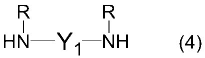
- diamines include diamines represented by the following formula (4) (however, diamines of the formulas (1) and (2) are excluded).
- Y 1 represents a divalent organic group, and two R's each independently represent a hydrogen atom or an alkyl group having 1 to 5 carbon atoms.
- Y 1 in formula (4) The preferred specific examples of Y 1 in formula (4) are shown below (Y1-1) to (Y1-18), but the present invention is not limited thereto.
- the diamine residue derived from the diamine of the formula (1) and the diamine of the formula (2) is preferably 50 mol% or more, and more preferably 60 mol% or more, of all diamine residues contained in the polymer (A).
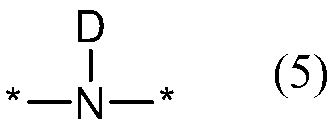
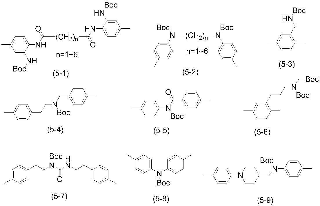
- the polymer (A) is likely to be unevenly distributed in the vicinity of the surface layer of the liquid crystal aligning film, so that the liquid crystal aligning property is improved. It is preferable to use at least one diamine having a structure of the following formula (5) for Y 1 in the above formula (4).
- D represents a protecting group that is eliminated by heating at 80 to 250° C., and particularly preferably 80 to 230° C. and is replaced with a hydrogen atom, and * represents a connection point with another structure.
- a preferable example of D is a t-butoxycarbonyl group.
- the residue of the diamine represented by the formula (4) is preferably 1 to 40 mol %, more preferably 5 to 30 mol% of all the diamine residues contained in the polymer (A). is there.
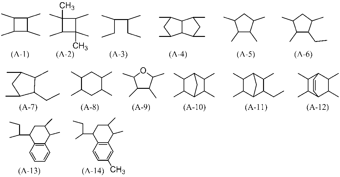
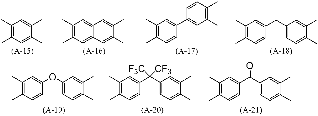
- the structure of the tetracarboxylic acid residue in the polymer (A) is not particularly limited. Moreover, the structure of the tetracarboxylic acid residue of the polymer (A) may be one type, or two or more types may be mixed.
- the molecular weight of the polymer (A) is not particularly limited as long as a good coating film can be formed, but for example, the weight average molecular weight is preferably 2,000 to 500,000, more preferably 5,000 to 300,000. , And more preferably 10,000 to 100,000.
- the number average molecular weight is preferably 1,000 to 250,000, more preferably 2,500 to 150,000, and further preferably 5,000 to 50,000.
- the polymer (B) is a polymer obtained by reacting a tetracarboxylic acid derivative component with a diamine component containing at least one diamine represented by the following formula (3).
- Y 2 is a divalent organic group having a nitrogen atom bonded to the aromatic group or a nitrogen-containing aromatic heterocycle.
- Y2-1 particularly preferable Y 2 structures (Y2-1) to (Y2-14) are shown below, but the present invention is not limited thereto.
- the structure of the diamine residue contained in the polymer (B) may be one type or two or more types may be mixed, but at least one type is the structure of Y 2 of the formula (3). ..
- the diamine residue having the structure of Y 2 is preferably 50 mol% or more, and more preferably 60 mol% or more of all the diamine residues contained in the polymer (B).
- the polymer (B) may have a diamine residue derived from another diamine other than the diamine represented by the formula (3).
- a compound represented by the above formula (4) which is the other diamine in the polymer (A) (however, excluding the diamine represented by the formula (3)) can be used.
- the amounts of the other diamines used in this case are the same as in the case of the polymer (A).
- the structure of the tetracarboxylic acid residue in the polymer (B) is not particularly limited. Moreover, the structure of the tetracarboxylic acid residue of the polymer (B) may be one type, or two or more types may be mixed. Examples of the preferable structure of the tetracarboxylic acid residue in the polymer (B) include the preferable structures shown in the polymer (A), but the present invention is not limited thereto.
- the molecular weight of the polymer (B) is not particularly limited as long as a good coating film can be formed, but for example, the weight average molecular weight is preferably 2,000 to 500,000, more preferably 5,000 to 300,000. , And more preferably 10,000 to 100,000.
- the number average molecular weight is preferably 1,000 to 250,000, more preferably 2,500 to 150,000, and further preferably 5,000 to 50,000.
- the content ratio of the polymer (A) and the polymer (B) in the liquid crystal aligning agent of the present invention is not particularly limited, but the polymer (A) relative to the total amount of the polymer (A) and the polymer (B).
- the content of is preferably 10 to 50% by mass, more preferably 20 to 40% by mass. That is, the content of the polymer (B) is preferably 90 to 50% by mass, and more preferably 80 to 60% by mass, based on the total amount of the polymer (A) and the polymer (B). preferable.
- the liquid crystal aligning agent of the present invention may contain a polymer other than the polymer (A) and the polymer (B).
- Other polymers are not particularly limited, but mainly include, for example, polyamic acid, polyamic acid ester, polyimide, polysiloxane, polyester, cellulose derivative, polyacetal, polystyrene derivative, poly(styrene-maleimide) derivative, and poly(meth)acrylate. Examples thereof include polymers having a skeleton.
- the liquid crystal aligning agent of the present invention may contain components other than the polymer.
- a dielectric material or a conductive substance for the purpose of changing the electrical properties such as the dielectric constant and conductivity of the liquid crystal alignment film, and a silane coupling agent for the purpose of improving the adhesion between the liquid crystal alignment film and the substrate.
- a crosslinkable compound for the purpose of increasing the hardness and the density of the film when it is formed into a liquid crystal alignment film, and further an imidization promoter for the purpose of efficiently promoting the imidization of polyamic acid when baking the coating film. Be done.
- the liquid crystal aligning agent of the present invention is used for producing a liquid crystal aligning film, and from the viewpoint of forming a uniform thin film, a coating liquid in which the above components are dissolved in an organic solvent is preferable.
- the concentration of the coating liquid is appropriately changed depending on the coating device used and the thickness of the liquid crystal alignment film to be obtained. From the viewpoint of forming a uniform and defect-free coating film, it is preferably 1% by mass or more, and from the viewpoint of storage stability of the solution, it is preferably 10% by mass or less.
- a particularly preferable polymer concentration is 2 to 8% by mass.
- the organic solvent used in the coating liquid is not particularly limited as long as the polymer component can be uniformly dissolved therein.
- Specific examples thereof include N,N-dimethylformamide, N,N-dimethylacetamide, N-methyl-2-pyrrolidone, N-ethyl-2-pyrrolidone, dimethyl sulfoxide, ⁇ -butyrolactone and 1,3-dimethyl.
- -Imidazolidinone, methyl ethyl ketone, cyclohexanone, cyclopentanone and the like can be mentioned.
- N-methyl-2-pyrrolidone, N-ethyl-2-pyrrolidone, or ⁇ -butyrolactone is preferable. Two or more kinds of these solvents may be used in combination.
- a mixed solvent obtained by adding a solvent that improves the coating property and the smoothness of the coating film surface in addition to the above solvent is also suitably used in the liquid crystal aligning agent of the present invention.
- Specific examples of the organic solvent to be mixed are given below, but the organic solvent is not limited to these examples.
- ethanol isopropyl alcohol, 1-butanol, 2-butanol, isobutyl alcohol, tert-butyl alcohol, 1-pentanol, 2-pentanol, 3-pentanol, 2-methyl-1-butanol, isopentyl alcohol, tert-pentyl alcohol, 3-methyl-2-butanol, neopentyl alcohol, 1-hexanol, 2-methyl-1-pentanol, 2-methyl-2-pentanol, 2-ethyl-1-butanol, 1-heptanol , 2-heptanol, 3-heptanol, 1-octanol, 2-octanol, 2-ethyl-1-hexanol, cyclohexanol, 1-methylcyclohexanol, 2-methylcyclohexanol, 3-methylcyclohexanol, 1,2- Ethanediol, 1,2-propanediol,
- R in the formulas [D-1] and [D-2] represents an alkyl group having 1 to 3 carbon atoms
- R in the formula [D-3] represents an alkyl group having 1 to 4 carbon atoms.
- 1-hexanol, cyclohexanol, 1,2-ethanediol, 1,2-propanediol, propylene glycol monobutyl ether, diethylene glycol diethyl ether, 4-hydroxy-4-methyl-2-pentanone, ethylene glycol mono Butyl ether or dipropylene glycol dimethyl ether are preferred.
- the type and content of such a solvent are appropriately selected depending on the application device of the liquid crystal alignment agent, the application conditions, the application environment, and the like. Further, two or more kinds of these solvents may be used in combination.
- the liquid crystal alignment film of the present invention is obtained from the above liquid crystal aligning agent of the present invention.
- a liquid crystal alignment agent in the form of a coating liquid is applied to a substrate, dried, and baked to obtain a film, which is subjected to a rubbing treatment method or an optical alignment treatment method.
- the method of performing the alignment treatment may be mentioned.
- the substrate on which the liquid crystal aligning agent is applied is not particularly limited, and a glass substrate, a silicon nitride substrate, a plastic substrate such as an acrylic substrate or a polycarbonate substrate, or the like can be used. At that time, it is preferable to use a substrate on which an ITO electrode or the like for driving the liquid crystal is formed, from the viewpoint of simplifying the process. Further, in the reflection type liquid crystal display element, an opaque material such as a silicon wafer can be used if only one substrate is used, and in this case, a material that reflects light such as aluminum can also be used for the electrode.
- the method for applying the liquid crystal aligning agent is not particularly limited, but industrially, screen printing, offset printing, flexo printing, inkjet method and the like are generally used. Other coating methods include a dip method, a roll coater method, a slit coater method, a spinner method, and a spray method, and these may be used depending on the purpose.
- the solvent is evaporated and baked by a heating means such as a hot plate, a heat circulation type oven, an IR (infrared) type oven. Any temperature and time can be selected for the drying and baking steps after applying the liquid crystal aligning agent.
- a heating means such as a hot plate, a heat circulation type oven, an IR (infrared) type oven. Any temperature and time can be selected for the drying and baking steps after applying the liquid crystal aligning agent.
- the conditions include baking at 50 to 120° C. for 1 to 10 minutes and then baking at 150 to 300° C. for 5 to 120 minutes.
- the thickness of the liquid crystal alignment film after firing is not particularly limited, but if it is too thin, the reliability of the liquid crystal display element may decrease, so that it is preferably 5 to 300 nm, more preferably 10 to 200 nm.
- the liquid crystal alignment film of the present invention is suitable as a liquid crystal alignment film of a horizontal electric field type liquid crystal display device such as an IPS system or an FFS system, and is particularly useful as a liquid crystal alignment film of an FFS system liquid crystal display device.
- the liquid crystal display device of the present invention is a device obtained by preparing a liquid crystal cell by a known method after obtaining a substrate with a liquid crystal alignment film obtained from the above liquid crystal aligning agent.
- An example of a method for producing a liquid crystal cell will be given below, but the present invention is not limited to this.
- This electrode can be, for example, an ITO electrode and is patterned so as to display a desired image.
- a switching element such as a TFT (Thin Film Transistor) may be provided in each pixel portion forming the image display.
- the liquid crystal alignment film is formed on this substrate as described above.
- an ultraviolet-curable sealing material is arranged at a predetermined position on one of the two substrates having the liquid crystal alignment film formed thereon, and liquid crystals are further arranged at predetermined positions on the surface of the liquid crystal alignment film.
- the other substrate is pasted and pressure-bonded so that the liquid crystal alignment film faces each other to spread the liquid crystal on the front face of the liquid crystal alignment film, and then the entire surface of the substrate is irradiated with ultraviolet rays to cure the sealing material. Get the cell.
- an opening that can be filled with liquid crystal from the outside is provided when the sealing material is arranged at a predetermined position on one of the substrates.
- the liquid crystal material is injected into the liquid crystal cell through the opening provided in the sealing material, and then the opening is sealed with an adhesive to obtain a liquid crystal cell.
- the liquid crystal material may be injected by a vacuum injection method or a method utilizing a capillary phenomenon in the atmosphere.
- columnar protrusions are provided on one substrate, spacers are scattered on one substrate, or a sealing material is used. It is preferable to take measures such as mixing a spacer with the above or combining them.
- the liquid crystal material may be a nematic liquid crystal or a smectic liquid crystal, of which a nematic liquid crystal is preferable, and either a positive type liquid crystal material or a negative type liquid crystal material may be used.
- a polarizing plate is installed. Specifically, it is preferable to attach a pair of polarizing plates to the surfaces of the two substrates opposite to the liquid crystal layer.
- NMP N-methyl-2-pyrrolidone
- BCS butyl cellosolve
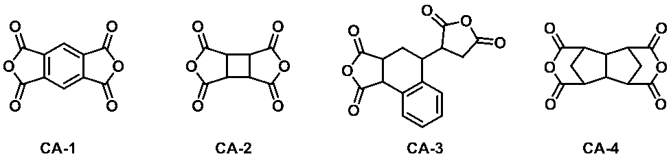
- CA-1 to CA-4 compounds of the following structural formulas
- DA-1 to DA-6 compounds of the following structural formulas
- AD-1 3-glycid Xypropyltriethoxysilane
- AD-2 Compound of the following structural formula
- the viscosity of the polymer solution was measured using an E-type viscometer TVE-22H (manufactured by Toki Sangyo Co., Ltd.) with a sample amount of 1.1 mL, a cone rotor TE-1 (1°34', R24), and a temperature of 25°C.
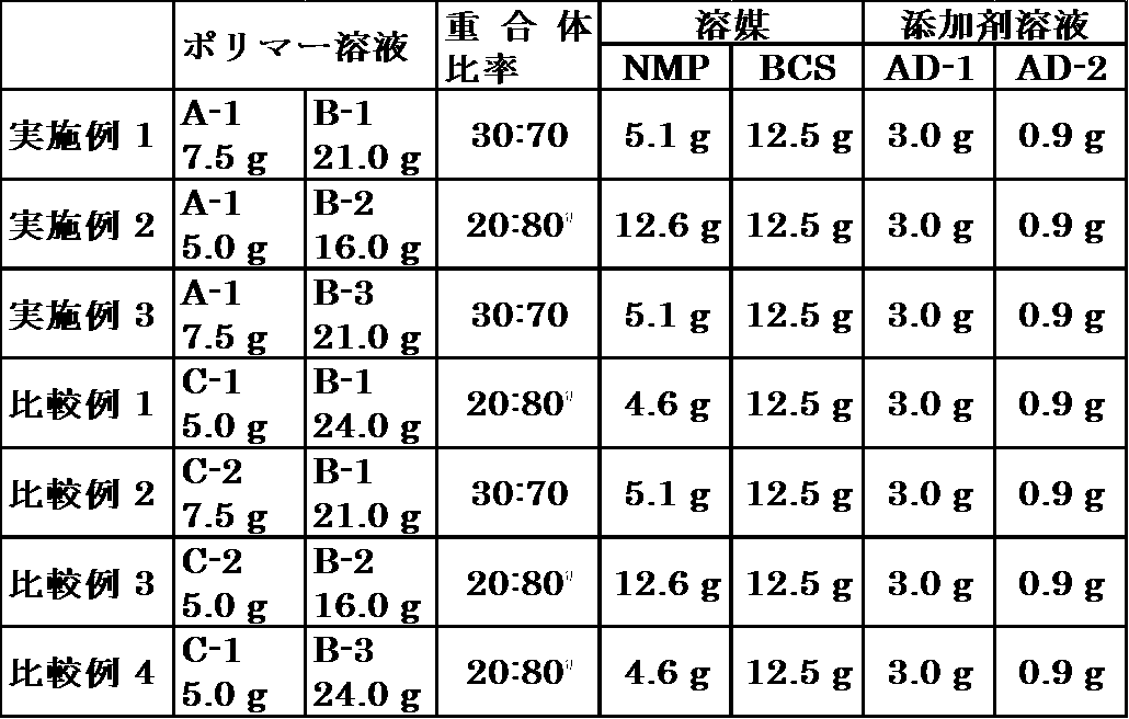
- Example 1 Using the polymer solution A-1 and the polymer solution B-1, the polymer solution A-1 (7.5 g) and the polymer solution B-1 (so that the mass ratio of the two kinds of polymers is 30:70). 21.0 g) were mixed. Based on this mixed solution, NMP solution (5.1 g), BCS (12.5 g), NMP solution containing 3.0% by weight of AD-1 (3.0 g), and NMP solution containing 10% by weight of AD-2 (0 1.9 g) was added with stirring, and the mixture was further stirred at room temperature for 2 hours to obtain a liquid crystal aligning agent of the present invention.
- Example 2 and 3 and Comparative Examples 1 to 4 The same operation as in Example 1 was performed with the compositions shown in Table 1 below to obtain liquid crystal aligning agents of Examples 2 and 3 of the present invention and liquid crystal aligning agents of Comparative Examples 1 to 4.
- FFS-driving liquid crystal cell shown below was produced using the liquid crystal aligning agent obtained above.
- a FOP (Finger on Plate) electrode layer composed of a planar common electrode-insulating layer-comb-shaped pixel electrode is formed on the surface.
- One glass substrate and a second glass substrate having a columnar spacer having a height of 4 ⁇ m on the front surface and having an ITO film for preventing electrification formed on the back surface were set as a set.
- the pixel electrode has a comb-tooth shape in which a plurality of electrode elements each having a width of 3 ⁇ m and whose central portion is bent at an internal angle of 160° are arranged in parallel at intervals of 6 ⁇ m, and one pixel is It has a first region and a second region with a line connecting the bent portions of the plurality of electrode elements as a boundary.
- the liquid crystal alignment film formed on the first glass substrate is subjected to an alignment treatment so that the direction that evenly divides the interior angle of the bent portion of the pixel and the alignment direction of the liquid crystal are orthogonal to each other, and the liquid crystal alignment film formed on the second glass substrate.
- the film is subjected to an alignment treatment so that the alignment direction of the liquid crystal on the first substrate and the alignment direction of the liquid crystal on the second substrate coincide with each other when the liquid crystal cell is manufactured.
- a sealant is printed on one of the pair of substrates with the liquid crystal alignment film, and the other substrate is attached so that the liquid crystal alignment film surfaces face each other and the rubbing directions of the substrates are antiparallel.
- the sealing agent was cured to prepare an empty cell.
- Liquid crystal MLC-3019 manufactured by Merck Ltd.
- the obtained liquid crystal cell was heated at 120° C. for 1 hour and left overnight, and then various evaluations were performed.
- the VT curve (voltage-transmittance curve) was measured while applying an alternating voltage of 30 Hz to this liquid crystal cell, and the alternating voltage values at which the relative transmittances were 23% and 100% were calculated as the driving voltage. ..
- an alternating voltage of 20 mV was applied to the liquid crystal cell at 23° C. at a frequency of 1 kHz for 30 minutes.
- the minimum offset voltage value means a DC voltage value at which flicker is minimized by measuring a VF curve (voltage-flicker curve) when an AC voltage having a relative transmittance of 23% is applied.
- the AC voltage having a relative transmittance of 23% is used because this AC voltage value corresponds to a region in which the change in the luminance with respect to the voltage is large, which is convenient for evaluating the accumulated charge through the luminance. ..
- the charge storage amount was less than 100 mV, it was evaluated as “ ⁇ ”, and when it was 100 mV or more, it was evaluated as “x”.
- the FFS-driving liquid crystal cell produced above is placed between two polarizing plates arranged so that their polarization axes are orthogonal to each other, and the pixel electrode and the counter electrode are short-circuited to have the same potential.
- the LED backlight was irradiated from under the polarizing plate, and the angle of the liquid crystal cell was adjusted so that the brightness of the LED backlight transmitted light measured on the two polarizing plates was minimized. This evaluation was carried out under the temperature condition where the temperature of the liquid crystal cell was 23°C.
- the liquid crystal cell was evaluated after applying an alternating voltage of 20 mV at a frequency of 1 kHz for 30 minutes in order to eliminate the influence of charging.
- VT curve voltage-transmittance curve
- the relaxation characteristic of the accumulated charge is that the relative transmittance immediately after the DC voltage is superimposed is 30% or more. It evaluated by the time required until it fell to 23%. It can be said that the shorter this time is, the better the relaxation characteristic of the accumulated charge is.
- the time during which the relative transmittance decreased to 30% or less was quantified until 30 minutes passed from the time when the application of the DC voltage was started.
- the relative transmittance was reduced to 30% or less in less than 20 minutes, it was evaluated as “ ⁇ ”, and when it was 20 minutes or more, it was evaluated as “x”.
- a liquid crystal cell is installed between two polarizing plates arranged so that their polarization axes are orthogonal to each other, the backlight is turned on, and the liquid crystal cell is arranged so that the transmitted light intensity in the first region of the pixel is minimized.
- the arrangement angle was adjusted, and then the rotation angle required when the liquid crystal cell was rotated so that the transmitted light intensity of the second region of the pixel was minimized was obtained. It can be said that the smaller the value of the rotation angle, the better the afterimage characteristic due to the long-term AC drive. Specifically, when the rotation angle is less than 0.5 degrees, it is evaluated as “ ⁇ ”, and when it is 0.5 degrees or more, it is evaluated as “x”.
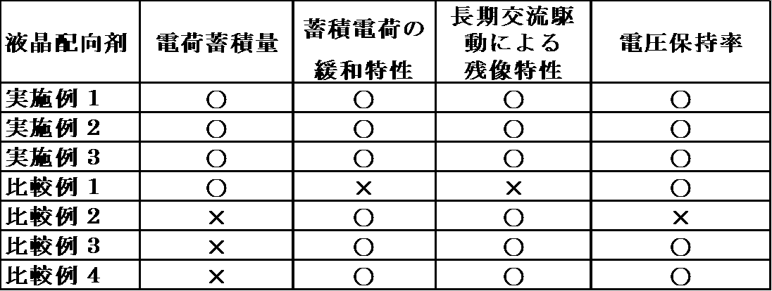
- Table 2 shows the evaluation results of the liquid crystal cells using the liquid crystal aligning agents of the Examples and Comparative Examples.
- the liquid crystal display device using the liquid crystal aligning agent of the present invention has a small amount of accumulated charge and a good relaxation property of accumulated charge.
- the entire contents of the specification, claims, drawings, and abstract of Japanese Patent Application No. 2018-229216 filed on Dec. 6, 2018 are cited herein as disclosure of the specification of the present invention. , Take in.
Landscapes
- Chemical & Material Sciences (AREA)
- Physics & Mathematics (AREA)
- Organic Chemistry (AREA)
- Nonlinear Science (AREA)
- Chemical Kinetics & Catalysis (AREA)
- Medicinal Chemistry (AREA)
- Polymers & Plastics (AREA)
- Health & Medical Sciences (AREA)
- Crystallography & Structural Chemistry (AREA)
- General Physics & Mathematics (AREA)
- Spectroscopy & Molecular Physics (AREA)
- Mathematical Physics (AREA)
- Optics & Photonics (AREA)
- Materials Engineering (AREA)
- Engineering & Computer Science (AREA)
- Liquid Crystal (AREA)
- Compositions Of Macromolecular Compounds (AREA)
- Macromolecular Compounds Obtained By Forming Nitrogen-Containing Linkages In General (AREA)
Abstract
Description
特に、横電界方式では、縦電界方式と比べると基板内に形成される電極部分が少ないため電圧保持率が低下しやすかったり、画素電極と共通電極との距離が近いことにより配向膜や液晶層に強い電界が作用するため電荷が蓄積しやすいなど、電圧保持率や電荷蓄積特性の不足による不都合が顕著となりやすい。また、横電界方式では、液晶の配向規制力が弱いと液晶を長時間駆動させた際に液晶が初期の配向状態に戻らなくなり、コントラストが低下したり残像の原因となったりするので液晶配向膜の配向規制力も重要となる。
上記のような横電界方式の課題に対して、高配向の重合体と低抵抗の重合体とを混合した液晶配向剤から得られる液晶配向膜を用いる方法が提案されている(特許文献1)。
以上のことを踏まえ、本発明は、横電界方式、特にFFS方式の液晶表示素子に用いるのに好適な液晶配向膜、更にはFFS方式であっても電荷の蓄積量が小さく且つ蓄積電荷の緩和が早い液晶配向膜を得ることができる液晶配向剤を提供することを課題とする。
重合体(A):テトラカルボン酸誘導体成分と、下記式(1)に示すジアミン及び下記式(2)に示すジアミンを含むジアミン成分との反応によって得られる重合体。



テトラカルボン酸誘導体の例としては、テトラカルボン酸二無水物、テトラカルボン酸ジシリルエステル、テトラカルボン酸ジクロライド、テトラカルボン酸ジアルキルエステル、テトラカルボン酸ジアルケニルエステル、テトラカルボン酸ジアルキルエステルジクロライドなどが挙げられる。
重合体(A)は、テトラカルボン酸誘導体成分と、下記式(1)に示すジアミン及び下記式(2)に示すジアミンを含むジアミン成分との(重縮合)反応によって得られる重合体である。


重合体(A)において、式(1)のジアミンに由来するジアミン残基は、重合体(A)が有する全ジアミン残基の10モル%以上であると好ましく、より好ましくは20モル%以上である。また、重合体(A)において、式(2)のジアミンに由来するジアミン残基は、重合体(A)が有する全ジアミン残基の30モル%以上であると好ましく、より好ましくは40モル%以上である。

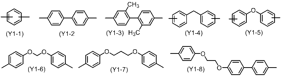
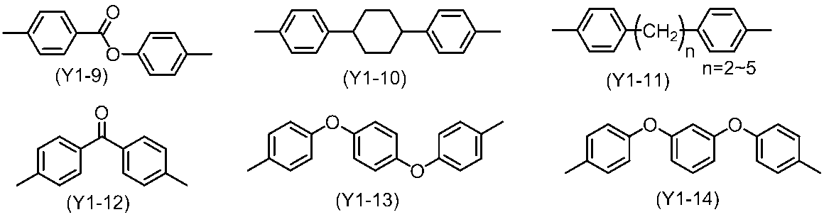

重合体(B)は、テトラカルボン酸誘導体成分と、下記式(3)で表されるジアミンの少なくとも1種を含むジアミン成分との反応によって得られる重合体である。

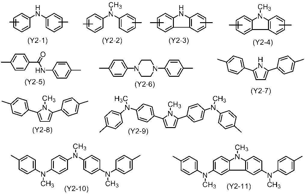

重合体(B)において、Y2の構造であるジアミン残基は、重合体(B)が有する全ジアミン残基の50モル%以上であると好ましく、より好ましくは60モル%以上である。
重合体(B)におけるテトラカルボン酸残基の好ましい構造としては、重合体(A)で示した好ましい構造が挙げられるが、本発明はこれらに限定されるものではない。
本発明の液晶配向剤における重合体(A)と重合体(B)の含有比率は特に限定されないが、重合体(A)と重合体(B)の合計量に対して、重合体(A)の含有量が10~50質量%が好ましく、更に好ましくは20~40質量%である。すなわち、重合体(B)の含有量は、重合体(A)と重合体(B)の合計量に対して、それぞれ、90~50質量%が好ましく、80~60質量%であるのが更に好ましい。

本発明の液晶配向膜は、上記本発明の液晶配向剤から得られる。液晶配向剤から液晶配向膜を得る方法の一例を挙げるなら、塗布液形態の液晶配向剤を基板に塗布し、乾燥し、焼成して得られた膜に対してラビング処理法又は光配向処理法で配向処理を施す方法が挙げられる。
液晶配向剤の塗布方法は、特に限定されないが、工業的には、スクリーン印刷、オフセット印刷、フレキソ印刷、インクジェット法などが一般的である。その他の塗布方法としては、ディップ法、ロールコータ法、スリットコータ法、スピンナー法、スプレー法などがあり、目的に応じてこれらを用いてもよい。
焼成後の液晶配向膜の厚みは、特に限定されないが、薄すぎると液晶表示素子の信頼性が低下する場合があるので、5~300nmが好ましく、10~200nmがより好ましい。
本発明の液晶配向膜は、IPS方式やFFS方式などの横電界方式の液晶表示素子の液晶配向膜として好適であり、特に、FFS方式の液晶表示素子の液晶配向膜として有用である。
本発明の液晶表示素子は、上記液晶配向剤から得られる液晶配向膜付きの基板を得た後、既知の方法で液晶セルを作製し、該液晶セルを使用して素子としたものである。
以下に、液晶セルの作製方法の一例を挙げるが、本発明はこれに限定されるものではない。
また、基板の上に液晶配向膜を形成した後の工程としては、一方の基板上の所定の場所にシール材を配置する際に、外部から液晶を充填可能な開口部を設けておき、液晶を配置しないで基板を貼り合わせた後、シール材に設けた開口部を通じて液晶セル内に液晶材料を注入し、次いで、この開口部を接着剤で封止して液晶セルを得る。液晶材料の注入には、真空注入法でもよいし、大気中で毛細管現象を利用した方法でもよい。
上記のいずれの方法においても、液晶セル内に液晶材料が充填される空間を確保する為に、一方の基板上に柱状の突起を設けるか、一方の基板上にスペーサーを散布するか、シール材にスペーサーを混入するか、又はこれらを組み合わせるなどの手段を取ることが好ましい。
CA-1~CA-4:それぞれ下記構造式の化合物、 DA-1~DA-6:それぞれ下記構造式の化合物
AD-1:3-グリシドキシプロピルトリエトキシシラン、 AD-2:下記構造式の化合物
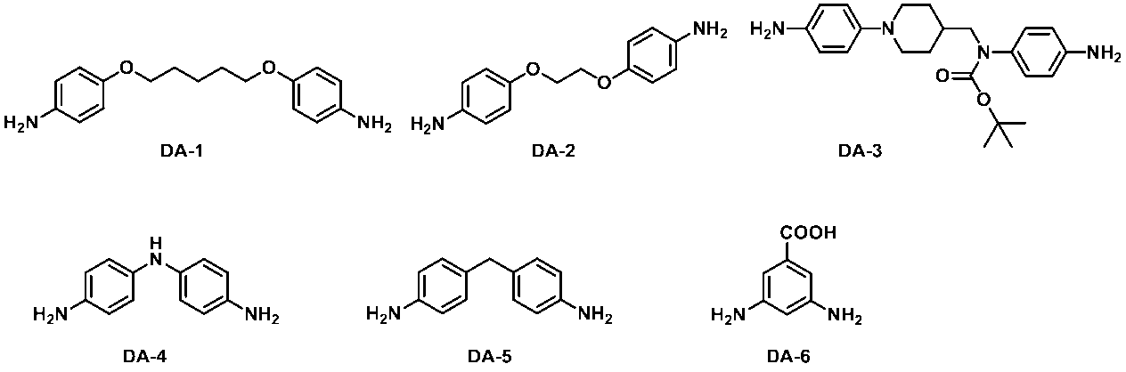
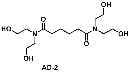
ポリマー溶液の粘度は、E型粘度計TVE-22H(東機産業社製)を用い、サンプル量1.1mL、コーンロータTE-1(1°34’、R24)、温度25℃で測定した。
(合成例1)
撹拌装置及び窒素導入管付きの100mLのナスフラスコに、DA-1を2.86g(10.0mmol)、DA-2を1.47g(6.0mmol)及びDA-3を1.59g(4.0mmol)量り取り、NMPを53.2g加え、窒素を送りながら撹拌して溶解させた。このジアミン溶液を水冷下で撹拌しながら、CA-1を4.20g(19.3mmol)添加し、さらにNMPを21.0g加え、窒素雰囲気下、50℃で12時間撹拌してポリマー溶液A-1(濃度:12.0質量%、粘度:496mPa・s)を得た。
撹拌装置及び窒素導入管付きの100mLのナスフラスコに、DA-4を3.19g(16.0mmol)及びDA-5を0.79g(4.0mmol)量り取り、NMPを49.0g加え、窒素を送りながら撹拌して溶解させた。このジアミン溶液を水冷下で撹拌しながら、CA-2を2.59g(13.2mmol)添加し、さらにNMPを13.9g加え、窒素雰囲気下23℃で2時間半撹拌した。その後、この溶液を水冷下で撹拌しながら、CA-3を1.20g(4.0mmol)添加し、さらにNMPを7.0g加え、窒素雰囲気下、23℃で12時間撹拌してポリマー溶液B-1(濃度:10.0質量%、粘度:165mPa・s)を得た。
撹拌装置及び窒素導入管付きの100mLのナスフラスコに、DA-4を3.67g(18.4mmol)及びDA-6を0.70g(4.6mmol)量り取り、NMPを26.8g加え、窒素を送りながら撹拌して溶解させた。このジアミン溶液を水冷下で撹拌しながら、CA-2を2.94g(15.0mmol)添加し、さらにNMPを14.5g加え、窒素雰囲気下23℃で30分撹拌した。その後、この溶液を水冷下で撹拌しながら、CA-4を1.44g(5.8mmol)添加し、さらにNMPを8.2g加え、窒素雰囲気下、50℃で12時間撹拌してポリマー溶液B-2(濃度:15.0質量%、粘度:352mPa・s)を得た。
撹拌装置及び窒素導入管付きの100mLのナスフラスコに、DA-4を3.19g(16mmol)及びDA-5を0.79g(4mmol)量り取り、NMPを54.4g加え、窒素を送りながら撹拌して溶解させた。このジアミン溶液を水冷下で撹拌しながら、CA-2を0.90g(4.6mmol)添加し、さらにNMPを15.5g加え、窒素雰囲気下23℃で30分撹拌した。その後、この溶液を水冷下で撹拌しながら、CA-4を3.75g(15.0mmol)添加し、さらにNMPを7.8g加え、窒素雰囲気下、50℃で12時間撹拌してポリマー溶液B-3(濃度:10.0質量%、粘度:218mPa・s)を得た。
撹拌装置及び窒素導入管付きの100mLのナスフラスコに、DA-1を5.73g(20.0mmol)量り取り、NMPを56.9g加え、窒素を送りながら撹拌して溶解させた。このジアミン溶液を水冷下で撹拌しながら、CA-1を3.97g(18.2mmol)添加し、さらにNMPを14.2g加え、窒素雰囲気下、50℃で12時間撹拌してポリマー溶液C-1(濃度:12.0質量%、粘度:505mPa・s)を得た。
撹拌装置及び窒素導入管付きの100mLのナスフラスコに、DA-1を4.13g(14.4mmol)及びDA-3を1.43g(3.6mmol)量り取り、NMPを53.3g加え、窒素を送りながら撹拌して溶解させた。このジアミン溶液を水冷下で撹拌しながら、CA-1を3.53g(16.2mmol)添加し、さらにNMPを13.3g加え、窒素雰囲気下、50℃で12時間撹拌してポリマー溶液C-2(濃度:12.0質量%、粘度:498mPa・s)を得た。
実施例1
前記ポリマー溶液A-1及び前記ポリマー溶液B-1を用い、2種類の重合体の質量比が30:70になるように、ポリマー溶液A-1(7.5g)とポリマー溶液B-1(21.0g)を混合した。この混合液に対して、NMP(5.1g)、BCS(12.5g)、AD-1を1重量%含むNMP溶液(3.0g)、及びAD-2を10重量%含むNMP溶液(0.9g)を、攪拌しながら加え、更に室温で2時間撹拌することにより本発明の液晶配向剤を得た。
下記の表1に示す組成にて、前記実施例1と同様の操作を行い、本発明の実施例2、3である液晶配向剤及び比較例1~4である液晶配向剤を得た。
前記で得られた液晶配向剤を用いて以下に示すFFS駆動液晶セルを作製した。
[FFS駆動液晶セルの構成]
フリンジフィールドスィッチング(Fringe Field Switching:FFS)モード用の液晶セルは、面形状の共通電極-絶縁層-櫛歯形状の画素電極からなるFOP(Finger on Plate)電極層が表面に形成されている第1のガラス基板と、表面に高さ4μmの柱状スペーサーを有し裏面に帯電防止の為のITO膜が形成されている第2のガラス基板とを、一組とした。上記の画素電極は、中央部分が内角160°で屈曲した幅3μmの電極要素が6μmの間隔を開けて平行になるように複数配列された櫛歯形状を有しており、1つの画素は、複数の電極要素の屈曲部を結ぶ線を境に第1領域と第2領域を有している。
なお、第1のガラス基板に形成する液晶配向膜は、画素屈曲部の内角を等分する方向と液晶の配向方向とが直交するように配向処理し、第2のガラス基板に形成する液晶配向膜は、液晶セルを作製した時に第1の基板上の液晶の配向方向と第2の基板上の液晶の配向方向とが一致するように配向処理する。
上記一組のガラス基板それぞれの表面に、孔径1.0μmのフィルターで濾過した液晶配向剤をスピンコート塗布にて塗布し80℃のホットプレート上で2分間乾燥させた。その後、230℃の熱風循環式オーブンで30分間焼成を行い、膜厚100nmの液晶配向膜付き基板を得た。この液晶配向膜付き基板表面をレーヨン布(吉川化工社製、YA-20R)でラビング(ローラー直径:120mm、ローラー回転数:1000rpm、移動速度:20mm/sec、押し込み長:0.4mm)した後、純水中にて1分間超音波照射をして洗浄を行い、エアブローにて水滴を除去した後、80℃で15分間乾燥して液晶配向膜付き基板を得た。
前記で作製した液晶セルの特性を以下のようにして評価した。
[電荷蓄積量]
上記で作製したFFS駆動液晶セルに対し、偏光軸が直交するように配置された2枚の偏光板の間に設置し、画素電極と対向電極とを短絡して同電位にした状態で、2枚の偏光板の下からLEDバックライトを照射しておき、2枚の偏光板の上で測定するLEDバックライト透過光の輝度が最小となるように、液晶セルの角度を調節した。本評価は液晶セルの温度が23℃の状態の温度条件下で行った。
次にこの液晶セルに周波数30Hzの交流電圧を印加しながらV-Tカーブ(電圧-透過率曲線)を測定し、相対透過率が23%および100%となる交流電圧値を駆動電圧として算出した。次いで、帯電による影響を排除するために、液晶セルを23℃にて、周波数1kHzで20mVの交流電圧を30分間印加した。
蓄積された電荷が液晶配向の乱れや残像として表示に影響を与え、液晶素子の表示品位を著しく低下させるため、駆動時に生じる電荷蓄積量が小さい程、良好であると言える。具体的には、電荷蓄積量が100mV未満となる場合は「○」、100mV以上となる場合は「×」として評価した。
上記で作製したFFS駆動液晶セルに対し、偏光軸が直交するように配置された2枚の偏光板の間に設置し、画素電極と対向電極とを短絡して同電位にした状態で、2枚の偏光板の下からLEDバックライトを照射しておき、2枚の偏光板の上で測定するLEDバックライト透過光の輝度が最小となるように、液晶セルの角度を調節した。本評価は液晶セルの温度が23℃の状態の温度条件下で行った。液晶セルは、帯電による影響を排除するために、液晶セルを周波数1kHzで20mVの交流電圧を30分間印加した後に評価を行った。
次にこの液晶セルに周波数30Hzの交流電圧を印加しながらV-Tカーブ(電圧-透過率曲線)を測定し、相対透過率が23%となる交流電圧値を駆動電圧として算出した。この交流電圧値は電圧に対する輝度の変化が大きい領域に相当するため、輝度を介して蓄積電荷を評価するのに都合がよい。
蓄積した電荷の緩和が速いほど、直流電圧を重畳したときの液晶セルへの電荷蓄積も速いことから、蓄積電荷の緩和特性は、直流電圧を重畳した直後の相対透過率が30%以上の状態から23%に低下するまでに要した時間で評価した。この時間が短いほど蓄積電荷の緩和特性が良好であると言える。具体的には、直流電圧の印加を開始した時点から30分間が経過するまでに、相対透過率が30%以下に低下した時間を数値化した。20分未満で相対透過率が30%以下に低下した場合は「○」、20分以上となる場合は「×」として評価した。
上記で作製したFFS駆動液晶セルに対し、60℃の恒温環境下、周波数60Hzで±5Vの交流電圧を120時間印加した。その後、液晶セルの画素電極と対向電極との間をショートさせた状態にし、そのまま室温に一日放置した。
上記の処理を行った液晶セルに関して、電圧無印加状態における、画素の第1領域の液晶の配向方向と第2領域の液晶の配向方向とのずれを角度として算出した。
長期交流駆動による残像特性は、この回転角度の値が小さいほど良好であると言える。具体的には、回転角度が0.5度未満となる場合は「○」、0.5度以上となる場合には「×」として評価した。
上記で作製したFFS駆動液晶セルに対し、電圧保持率評価用の液晶表示素子に、1Vの電圧を60マイクロ秒の印加時間、1667ミリ秒の間隔で印加した後、印加解除から1667ミリ秒後の電圧保持率(%)を60℃で測定した。具体的には、電圧保持率が95%以上となる場合は「○」、95%未満となる場合には「×」として評価した。
前記実施例及び比較例の各液晶配向剤を使用した液晶セルの評価結果を下記表2に示す。
なお、2018年12月6日に出願された日本特許出願2018-229216号の明細書、特許請求の範囲、図面、及び要約書の全内容をここに引用し、本発明の明細書の開示として、取り入れるものである。
Claims (11)
- 下記の重合体(A)および重合体(B)を含有する液晶配向剤。
重合体(A):テトラカルボン酸誘導体成分と、下記式(1)に示すジアミン及び下記式(2)に示すジアミンを含むジアミン成分との反応によって得られる重合体。



- 前記重合体(A)及び/又は重合体(B)におけるジアミン成分が、更に、下記式(4)で表されるジアミンの少なくとも1種を含有する、請求項1に記載の液晶配向剤。
- 前記重合体(A)におけるジアミン成分が、式(4)におけるY1が下記式(5)の構造を有する2価の有機基であるジアミンを含有する、請求項2に記載の液晶配向剤。

- 前記重合体(A)における式(1)のジアミンに由来するジアミン残基は、重合体(A)が有する全ジアミン残基の10モル%以上であり、式(2)のジアミンに由来するジアミン残基は、重合体(A)が有する全ジアミン残基の30モル%以上である、請求項1~3のいずれかに記載の液晶配向剤。
- 前記重合体(A)と重合体(B)の合計量に対して、重合体(A)の含有量が10~50質量%であり、重合体(B)の含有量が90~50質量%である、請求項1~4のいずれかに記載の液晶配向剤。
- 横電界駆動方式の液晶表示素子用である、請求項1~5のいずれかに記載の液晶配向剤。
- 横電界駆動方式が、FFS駆動方式である、請求項1~6のいずれかに記載の液晶配向剤。
- 請求項1~7のいずれかに記載の液晶配向剤から得られる液晶配向膜。
- 請求項8に記載の液晶配向膜を有する液晶表示素子。
- 横電界駆動方式である、請求項9に記載の液晶表示素子。
- FFS駆動方式である、請求項9に記載の液晶表示素子。
Priority Applications (3)
| Application Number | Priority Date | Filing Date | Title |
|---|---|---|---|
| CN201980080517.7A CN113168054B (zh) | 2018-12-06 | 2019-12-05 | 液晶取向剂、液晶取向膜以及使用了该液晶取向膜的液晶显示元件 |
| JP2020560026A JP7435469B2 (ja) | 2018-12-06 | 2019-12-05 | 液晶配向剤、液晶配向膜及びそれを用いた液晶表示素子 |
| KR1020217016819A KR102779394B1 (ko) | 2018-12-06 | 2019-12-05 | 액정 배향제, 액정 배향막 및 그것을 이용한 액정 표시 소자 |
Applications Claiming Priority (2)
| Application Number | Priority Date | Filing Date | Title |
|---|---|---|---|
| JP2018229216 | 2018-12-06 | ||
| JP2018-229216 | 2018-12-06 |
Publications (1)
| Publication Number | Publication Date |
|---|---|
| WO2020116585A1 true WO2020116585A1 (ja) | 2020-06-11 |
Family
ID=70975476
Family Applications (1)
| Application Number | Title | Priority Date | Filing Date |
|---|---|---|---|
| PCT/JP2019/047701 Ceased WO2020116585A1 (ja) | 2018-12-06 | 2019-12-05 | 液晶配向剤、液晶配向膜及びそれを用いた液晶表示素子 |
Country Status (5)
| Country | Link |
|---|---|
| JP (1) | JP7435469B2 (ja) |
| KR (1) | KR102779394B1 (ja) |
| CN (1) | CN113168054B (ja) |
| TW (1) | TWI829822B (ja) |
| WO (1) | WO2020116585A1 (ja) |
Cited By (2)
| Publication number | Priority date | Publication date | Assignee | Title |
|---|---|---|---|---|
| KR20240032874A (ko) | 2021-07-12 | 2024-03-12 | 닛산 가가쿠 가부시키가이샤 | 액정 배향제, 액정 배향막, 액정 표시 소자의 제조 방법 및 액정 표시 소자 |
| KR20240032873A (ko) | 2021-07-12 | 2024-03-12 | 닛산 가가쿠 가부시키가이샤 | 액정 배향제, 액정 배향막, 액정 표시 소자의 제조 방법 및 액정 표시 소자 |
Citations (2)
| Publication number | Priority date | Publication date | Assignee | Title |
|---|---|---|---|---|
| WO2015060363A1 (ja) * | 2013-10-23 | 2015-04-30 | 日産化学工業株式会社 | 液晶配向剤、液晶配向膜、及び液晶配向素子 |
| WO2018062440A1 (ja) * | 2016-09-29 | 2018-04-05 | 日産化学工業株式会社 | 液晶配向剤、液晶配向膜、及び液晶表示素子 |
Family Cites Families (3)
| Publication number | Priority date | Publication date | Assignee | Title |
|---|---|---|---|---|
| US20060142538A1 (en) | 2002-12-11 | 2006-06-29 | Nissan Chemical Industries, Ltd. | Liquid crystal orientating agent and liquid crystal display element using it |
| JP6160218B2 (ja) * | 2012-08-03 | 2017-07-12 | Jsr株式会社 | 液晶配向剤、液晶配向膜、液晶表示素子及び液晶配向膜の製造方法 |
| JP7114856B2 (ja) * | 2016-02-15 | 2022-08-09 | 日産化学株式会社 | 液晶配向剤、液晶配向膜、及び液晶表示素子 |
-
2019
- 2019-12-05 JP JP2020560026A patent/JP7435469B2/ja active Active
- 2019-12-05 KR KR1020217016819A patent/KR102779394B1/ko active Active
- 2019-12-05 CN CN201980080517.7A patent/CN113168054B/zh active Active
- 2019-12-05 WO PCT/JP2019/047701 patent/WO2020116585A1/ja not_active Ceased
- 2019-12-06 TW TW108144596A patent/TWI829822B/zh active
Patent Citations (2)
| Publication number | Priority date | Publication date | Assignee | Title |
|---|---|---|---|---|
| WO2015060363A1 (ja) * | 2013-10-23 | 2015-04-30 | 日産化学工業株式会社 | 液晶配向剤、液晶配向膜、及び液晶配向素子 |
| WO2018062440A1 (ja) * | 2016-09-29 | 2018-04-05 | 日産化学工業株式会社 | 液晶配向剤、液晶配向膜、及び液晶表示素子 |
Cited By (2)
| Publication number | Priority date | Publication date | Assignee | Title |
|---|---|---|---|---|
| KR20240032874A (ko) | 2021-07-12 | 2024-03-12 | 닛산 가가쿠 가부시키가이샤 | 액정 배향제, 액정 배향막, 액정 표시 소자의 제조 방법 및 액정 표시 소자 |
| KR20240032873A (ko) | 2021-07-12 | 2024-03-12 | 닛산 가가쿠 가부시키가이샤 | 액정 배향제, 액정 배향막, 액정 표시 소자의 제조 방법 및 액정 표시 소자 |
Also Published As
| Publication number | Publication date |
|---|---|
| TW202031881A (zh) | 2020-09-01 |
| CN113168054B (zh) | 2025-03-04 |
| JPWO2020116585A1 (ja) | 2021-10-21 |
| JP7435469B2 (ja) | 2024-02-21 |
| KR20210099569A (ko) | 2021-08-12 |
| CN113168054A (zh) | 2021-07-23 |
| TWI829822B (zh) | 2024-01-21 |
| KR102779394B1 (ko) | 2025-03-10 |
Similar Documents
| Publication | Publication Date | Title |
|---|---|---|
| KR20160077083A (ko) | 액정 배향제, 액정 배향막, 및 액정 배향 소자 | |
| TWI772371B (zh) | 液晶配向劑、液晶配向膜及液晶顯示元件 | |
| JPWO2019082975A1 (ja) | 液晶配向剤、液晶配向膜及び液晶表示素子 | |
| WO2020040089A1 (ja) | 液晶配向剤、その製造方法、液晶配向膜、及び液晶表示素子 | |
| WO2020054797A1 (ja) | 液晶配向剤、液晶配向膜及び液晶表示素子並びにジアミン及びその製造方法並びに重合体 | |
| WO2018030489A1 (ja) | 液晶配向剤、液晶配向膜及び液晶表示素子 | |
| JP7435469B2 (ja) | 液晶配向剤、液晶配向膜及びそれを用いた液晶表示素子 | |
| CN114651207B (zh) | 液晶取向剂、液晶取向膜以及使用该液晶取向膜的液晶显示元件 | |
| CN111344630B (zh) | 液晶取向剂、液晶取向膜和液晶表示元件 | |
| JP7243628B2 (ja) | 液晶配向剤、液晶配向膜及びそれを用いた液晶表示素子 | |
| WO2018051956A1 (ja) | 液晶配向剤、液晶配向膜、及び液晶表示素子 | |
| WO2018066607A1 (ja) | ジアミン、重合体、液晶配向剤、液晶配向膜及び液晶表示素子 | |
| JPWO2019198671A1 (ja) | 液晶配向剤、液晶配向膜及びそれを用いた液晶表示素子 | |
| WO2018225810A1 (ja) | 液晶配向剤、液晶配向膜及び液晶表示素子 | |
| JP7571730B2 (ja) | 液晶配向剤、液晶配向膜及びそれを用いた液晶表示素子 | |
| CN109716223B (zh) | 具有液晶取向膜的基板的制造方法以及液晶表示元件 | |
| JP7022350B2 (ja) | 液晶配向剤、液晶配向膜および液晶表示素子 | |
| WO2020040091A1 (ja) | 液晶配向剤、その製造方法、液晶配向膜、及び液晶表示素子 | |
| CN111868619A (zh) | 液晶取向剂、液晶取向膜及液晶表示元件 | |
| JPWO2020121979A1 (ja) | 液晶配向剤、液晶配向膜及び液晶表示素子 |
Legal Events
| Date | Code | Title | Description |
|---|---|---|---|
| 121 | Ep: the epo has been informed by wipo that ep was designated in this application |
Ref document number: 19893485 Country of ref document: EP Kind code of ref document: A1 |
|
| ENP | Entry into the national phase |
Ref document number: 2020560026 Country of ref document: JP Kind code of ref document: A |
|
| ENP | Entry into the national phase |
Ref document number: 20217016819 Country of ref document: KR Kind code of ref document: A |
|
| NENP | Non-entry into the national phase |
Ref country code: DE |
|
| 122 | Ep: pct application non-entry in european phase |
Ref document number: 19893485 Country of ref document: EP Kind code of ref document: A1 |
|
| WWG | Wipo information: grant in national office |
Ref document number: 201980080517.7 Country of ref document: CN |