WO2020103605A1 - 一种选择性刻蚀生长基底制备悬空石墨烯支撑膜的方法 - Google Patents
一种选择性刻蚀生长基底制备悬空石墨烯支撑膜的方法Info
- Publication number
- WO2020103605A1 WO2020103605A1 PCT/CN2019/110916 CN2019110916W WO2020103605A1 WO 2020103605 A1 WO2020103605 A1 WO 2020103605A1 CN 2019110916 W CN2019110916 W CN 2019110916W WO 2020103605 A1 WO2020103605 A1 WO 2020103605A1
- Authority
- WO
- WIPO (PCT)
- Prior art keywords
- graphene
- growth
- support film
- film
- photoresist
- Prior art date
- Legal status (The legal status is an assumption and is not a legal conclusion. Google has not performed a legal analysis and makes no representation as to the accuracy of the status listed.)
- Ceased
Links
Images


Classifications
-
- C—CHEMISTRY; METALLURGY
- C01—INORGANIC CHEMISTRY
- C01B—NON-METALLIC ELEMENTS; COMPOUNDS THEREOF; METALLOIDS OR COMPOUNDS THEREOF NOT COVERED BY SUBCLASS C01C
- C01B32/00—Carbon; Compounds thereof
- C01B32/15—Nano-sized carbon materials
- C01B32/182—Graphene
- C01B32/194—After-treatment
-
- C—CHEMISTRY; METALLURGY
- C30—CRYSTAL GROWTH
- C30B—SINGLE-CRYSTAL GROWTH; UNIDIRECTIONAL SOLIDIFICATION OF EUTECTIC MATERIAL OR UNIDIRECTIONAL DEMIXING OF EUTECTOID MATERIAL; REFINING BY ZONE-MELTING OF MATERIAL; PRODUCTION OF A HOMOGENEOUS POLYCRYSTALLINE MATERIAL WITH DEFINED STRUCTURE; SINGLE CRYSTALS OR HOMOGENEOUS POLYCRYSTALLINE MATERIAL WITH DEFINED STRUCTURE; AFTER-TREATMENT OF SINGLE CRYSTALS OR A HOMOGENEOUS POLYCRYSTALLINE MATERIAL WITH DEFINED STRUCTURE; APPARATUS THEREFOR
- C30B25/00—Single-crystal growth by chemical reaction of reactive gases, e.g. chemical vapour-deposition growth
- C30B25/02—Epitaxial-layer growth
-
- C—CHEMISTRY; METALLURGY
- C30—CRYSTAL GROWTH
- C30B—SINGLE-CRYSTAL GROWTH; UNIDIRECTIONAL SOLIDIFICATION OF EUTECTIC MATERIAL OR UNIDIRECTIONAL DEMIXING OF EUTECTOID MATERIAL; REFINING BY ZONE-MELTING OF MATERIAL; PRODUCTION OF A HOMOGENEOUS POLYCRYSTALLINE MATERIAL WITH DEFINED STRUCTURE; SINGLE CRYSTALS OR HOMOGENEOUS POLYCRYSTALLINE MATERIAL WITH DEFINED STRUCTURE; AFTER-TREATMENT OF SINGLE CRYSTALS OR A HOMOGENEOUS POLYCRYSTALLINE MATERIAL WITH DEFINED STRUCTURE; APPARATUS THEREFOR
- C30B25/00—Single-crystal growth by chemical reaction of reactive gases, e.g. chemical vapour-deposition growth
- C30B25/02—Epitaxial-layer growth
- C30B25/10—Heating of the reaction chamber or the substrate
-
- C—CHEMISTRY; METALLURGY
- C30—CRYSTAL GROWTH
- C30B—SINGLE-CRYSTAL GROWTH; UNIDIRECTIONAL SOLIDIFICATION OF EUTECTIC MATERIAL OR UNIDIRECTIONAL DEMIXING OF EUTECTOID MATERIAL; REFINING BY ZONE-MELTING OF MATERIAL; PRODUCTION OF A HOMOGENEOUS POLYCRYSTALLINE MATERIAL WITH DEFINED STRUCTURE; SINGLE CRYSTALS OR HOMOGENEOUS POLYCRYSTALLINE MATERIAL WITH DEFINED STRUCTURE; AFTER-TREATMENT OF SINGLE CRYSTALS OR A HOMOGENEOUS POLYCRYSTALLINE MATERIAL WITH DEFINED STRUCTURE; APPARATUS THEREFOR
- C30B25/00—Single-crystal growth by chemical reaction of reactive gases, e.g. chemical vapour-deposition growth
- C30B25/02—Epitaxial-layer growth
- C30B25/16—Controlling or regulating
- C30B25/165—Controlling or regulating the flow of the reactive gases
-
- C—CHEMISTRY; METALLURGY
- C30—CRYSTAL GROWTH
- C30B—SINGLE-CRYSTAL GROWTH; UNIDIRECTIONAL SOLIDIFICATION OF EUTECTIC MATERIAL OR UNIDIRECTIONAL DEMIXING OF EUTECTOID MATERIAL; REFINING BY ZONE-MELTING OF MATERIAL; PRODUCTION OF A HOMOGENEOUS POLYCRYSTALLINE MATERIAL WITH DEFINED STRUCTURE; SINGLE CRYSTALS OR HOMOGENEOUS POLYCRYSTALLINE MATERIAL WITH DEFINED STRUCTURE; AFTER-TREATMENT OF SINGLE CRYSTALS OR A HOMOGENEOUS POLYCRYSTALLINE MATERIAL WITH DEFINED STRUCTURE; APPARATUS THEREFOR
- C30B25/00—Single-crystal growth by chemical reaction of reactive gases, e.g. chemical vapour-deposition growth
- C30B25/02—Epitaxial-layer growth
- C30B25/18—Epitaxial-layer growth characterised by the substrate
-
- C—CHEMISTRY; METALLURGY
- C30—CRYSTAL GROWTH
- C30B—SINGLE-CRYSTAL GROWTH; UNIDIRECTIONAL SOLIDIFICATION OF EUTECTIC MATERIAL OR UNIDIRECTIONAL DEMIXING OF EUTECTOID MATERIAL; REFINING BY ZONE-MELTING OF MATERIAL; PRODUCTION OF A HOMOGENEOUS POLYCRYSTALLINE MATERIAL WITH DEFINED STRUCTURE; SINGLE CRYSTALS OR HOMOGENEOUS POLYCRYSTALLINE MATERIAL WITH DEFINED STRUCTURE; AFTER-TREATMENT OF SINGLE CRYSTALS OR A HOMOGENEOUS POLYCRYSTALLINE MATERIAL WITH DEFINED STRUCTURE; APPARATUS THEREFOR
- C30B29/00—Single crystals or homogeneous polycrystalline material with defined structure characterised by the material or by their shape
- C30B29/02—Elements
-
- C—CHEMISTRY; METALLURGY
- C30—CRYSTAL GROWTH
- C30B—SINGLE-CRYSTAL GROWTH; UNIDIRECTIONAL SOLIDIFICATION OF EUTECTIC MATERIAL OR UNIDIRECTIONAL DEMIXING OF EUTECTOID MATERIAL; REFINING BY ZONE-MELTING OF MATERIAL; PRODUCTION OF A HOMOGENEOUS POLYCRYSTALLINE MATERIAL WITH DEFINED STRUCTURE; SINGLE CRYSTALS OR HOMOGENEOUS POLYCRYSTALLINE MATERIAL WITH DEFINED STRUCTURE; AFTER-TREATMENT OF SINGLE CRYSTALS OR A HOMOGENEOUS POLYCRYSTALLINE MATERIAL WITH DEFINED STRUCTURE; APPARATUS THEREFOR
- C30B33/00—After-treatment of single crystals or homogeneous polycrystalline material with defined structure
- C30B33/02—Heat treatment
-
- B—PERFORMING OPERATIONS; TRANSPORTING
- B82—NANOTECHNOLOGY
- B82Y—SPECIFIC USES OR APPLICATIONS OF NANOSTRUCTURES; MEASUREMENT OR ANALYSIS OF NANOSTRUCTURES; MANUFACTURE OR TREATMENT OF NANOSTRUCTURES
- B82Y30/00—Nanotechnology for materials or surface science, e.g. nanocomposites
-
- B—PERFORMING OPERATIONS; TRANSPORTING
- B82—NANOTECHNOLOGY
- B82Y—SPECIFIC USES OR APPLICATIONS OF NANOSTRUCTURES; MEASUREMENT OR ANALYSIS OF NANOSTRUCTURES; MANUFACTURE OR TREATMENT OF NANOSTRUCTURES
- B82Y40/00—Manufacture or treatment of nanostructures
-
- C—CHEMISTRY; METALLURGY
- C01—INORGANIC CHEMISTRY
- C01B—NON-METALLIC ELEMENTS; COMPOUNDS THEREOF; METALLOIDS OR COMPOUNDS THEREOF NOT COVERED BY SUBCLASS C01C
- C01B2204/00—Structure or properties of graphene
- C01B2204/04—Specific amount of layers or specific thickness
Definitions
- the invention relates to a method for preparing a suspended graphene supporting film by selectively etching a growth substrate.
- graphene As a two-dimensional single-atomic material with high mechanical strength, high electrical conductivity, and high thermal conductivity, graphene has good application prospects in the fields of support membranes, filter membranes, and membranes.
- suspended graphene film can be used as a transmission electron microscope carrier to improve imaging resolution; suspended monolayer graphene can be directly used as a hydrogen isotope separation film to achieve the enrichment of hydrogen isotopes.
- chemical vapor deposition CVD
- CVD chemical vapor deposition
- the preparation methods of graphene support films mainly include the following categories: 1. Spin-coat polymer films (such as PMMA) on graphene grown by CVD method, and etch away the metal substrate to transfer the graphene to the suspended substrate. The polymer film is then removed to obtain suspended graphene. The integrity of the suspended graphene obtained by this method is low, and the polymer pollution is relatively serious; 2. Graphene is transferred to the gold net containing carbon film through isopropyl alcohol. Although this method can avoid polymer pollution, it is costly, the process is unstable, and graphene support films cannot be prepared on a large scale; 3.
- Polymer films such as PMMA
- the purpose of the present invention is to provide a method for preparing a suspended graphene support film by selectively etching a growth substrate.
- the graphene support film obtained by the method does not need any auxiliary support, and the graphene support film has high integrity, large hanging area, wide clean area, and can be prepared in batches.
- the method for preparing a suspended graphene support film provided by the present invention includes:
- step 2) Etching away the graphene film on the side of the metal substrate obtained in step 1), spin coating photoresist, and photolithography to obtain a graphene / metal substrate / photoresist composite;
- step 2) Suspend the graphene / metal substrate / photoresist composite obtained in step 2) on the liquid surface of the etching solution, the etching solution completely etches the metal substrate exposed in the photolithography step, and remove the photoresist, The suspended graphene support film is obtained.
- the metal substrate is a single crystal and / or polycrystalline substrate of a transition metal or a transition metal alloy; the transition metal is selected from at least one of copper, nickel, molybdenum, and gold; the transition The metal alloy is specifically a copper-nickel alloy;
- the thickness of the metal substrate is 10-30 ⁇ m
- the graphene film is a single-layer large-domain single-crystal graphene film, a double-layer graphene film or a few-layer graphene film; the few-layer graphene film is specifically a 2-5 layer graphene film;
- the growth method is chemical vapor deposition.
- the growth temperature is 980 ° C-1050 ° C; specifically, it may be 1030 ° C;
- the carrier gas is selected from at least one of hydrogen and argon;
- Carrier gas flow rate is 100 ⁇ 2000sccm; specifically 100 or 500sccm;
- the carbon source gas is methane, ethylene or ethane
- the flow rate of the carbon source gas is 1 to 10 sccm.
- the flow rate of the carrier gas is 100-1000 sccm
- Annealing conditions are: first annealing at 980 °C -1050 °C, 50-500sccm hydrogen for 0.5-8h, and then annealing at 50-500sccm argon for 10-60min;
- the annealing conditions specifically include annealing at 1030 ° C and 100 sccm hydrogen atmosphere for 30 minutes, maintaining the pressure at 100 Pa, and then annealing in 100 sccm argon gas for 30 minutes;
- the growth time is 2-5 hours; specifically 3 hours;
- the growth pressure is 100-1000Pa; specifically 500Pa;
- the flow rate of the carrier gas is 100-1000 sccm; specifically, 400 sccm;
- the annealing conditions are 980 °C -1050 °C, 50-500sccm hydrogen annealing for 0.5-8h; the annealing conditions are specifically annealing at 1030 °C and 100sccm hydrogen atmosphere for 30 minutes, and the pressure is maintained at 100Pa;
- the growth pressure is 500-2000Pa; specifically 1000Pa;
- Growth time is 1-4 hours; specifically 1.5 hours;
- the flow rate of the carrier gas is 500-2000 sccm
- the annealing condition is annealing at 50-500sccm hydrogen for 0.5-8h; the annealing condition is specifically annealing at 1030 ° C and 100sccm hydrogen atmosphere for 30 minutes, and the pressure is maintained at 100Pa;
- the growth pressure is 1000-4000Pa; specifically 2000Pa;
- the growth time is 1-3 hours.
- the growth of graphene can be carried out in a 1-4 inch diameter high temperature tube furnace, and can be combined with a roll-to-roll device;
- the etching method is air plasma etching; the excitation power is 100-500 watts; specifically 200 watts; the etching time is 2-5 minutes; specifically 3 minutes; the gas flow rate is 10-30 sccm ;
- the photoresist is a positive photoresist; the spin coating rate is 2000-7000 revolutions / minute; specifically 4000 revolutions / minute; the spin coating time is 50-70s; specifically 60s;
- the photolithography is exposure at 350nm-365nm ultraviolet or electron beam; the exposure time is 5-15s; specifically 10s;
- This photolithography step can form a circular pattern; in the circular pattern, the circular hole diameter is 5-20 microns; the circular pattern is specifically a circular hole array; in the circular hole array, the circular hole pattern translation period is specific 50-100 microns.
- the etching temperature is 20-60 ° C; specifically, 50-60 ° C;
- the etching solution is sodium persulfate solution, ferric chloride solution or aqua regia; the concentration is 0.05-0.2 mol / L; the volume ratio of nitric acid to hydrochloric acid in the aqua regia is specifically 1: 3.
- the removal of the photoresist includes: treatment with acetone, ethanol or N-methylpyrrolidone, followed by treatment with isopropanol.
- the transfer medium of the suspended graphene support film in different solvents is a metal grid
- the pore size of the metal grid is 10-100 ⁇ m.
- the suspended graphene support film prepared according to the above method also belongs to the protection scope of the present invention.
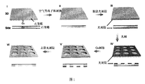
- Fig. 1 is a flow chart of a process for preparing a suspended graphene support film by selectively etching a graphene growth substrate according to the present invention.
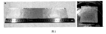
- FIG. 2 is a large-area graphene film prepared on a copper foil and a large-area graphene support film suspended on a liquid surface in Example 1.
- FIG. 3 is the SEM characterization results of the single-layer, double-layer, and few-layer (2-5 layers) graphene support films produced in Example 1.
- FIG. 3 is the SEM characterization results of the single-layer, double-layer, and few-layer (2-5 layers) graphene support films produced in Example 1.
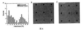
- FIG. 4 is the integrity statistics of the single-layer graphene single crystal thin film and the polycrystalline thin film in Example 1.
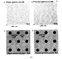
- FIG. 5 is a representative SEM characterization result of the two-layer graphene support film and the few-layer graphene support film in Example 1.
- FIG. The integrity of the two-layer and few-layer graphene support membranes is as high as 91% and 98%, respectively.
- FIG. 6 is a high-angle annular dark field-scanning transmission electron microscope (HAADF-STEM) imaging of an ultra-clean single-layer graphene support film in Example 1.
- HAADF-STEM high-angle annular dark field-scanning transmission electron microscope
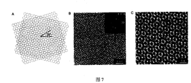
- Example 7 is an atomic resolution HAADF-STEM imaging of the ultra-clean double-layer graphene support film in Example 1, with a resolution of 1.07 Angstroms.
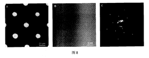
- Example 8 is a graphene support film prepared in Example 1 directly used as a transmission electron microscope support film.
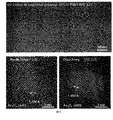
- Example 9 is a graphene support film produced in Example 1 used to support ferritin, and high-resolution imaging under a transmission electron microscope.
- copper foil is used as the metal substrate for growing graphene. Before growing graphene, the copper foil is subjected to electrochemical polishing.
- the circular hole array of photoresist in the following examples is made by a URE-2000 / 35 ultraviolet lithography machine, the exposure wavelength of the ultraviolet lamp is 365 nm, and the exposure time is 5-15 seconds.
- the positive photoresist model is AR-P5350.
- the developer model is AR 300-26, and the formula is 1: 7 water.
- the fixing solution is pure water.
- the prepared graphene and suspended graphene support films are characterized in the following examples, including the number of graphene layers, integrity, suspended size, cleanliness, and atomic structure.
- the measurement method is as follows:
- Graphene support film layer number, integrity and suspension size measurement using scanning electron microscopy (Hitachi S-4800) can characterize the number of suspended graphene support film layers, damage and the size of the suspension size.
- Graphene is transferred to a silicon wafer containing a 300 nm oxide layer, and the number of graphene layers can also be characterized using an optical microscope (Nikon, DS-Ri2).
- FIG. 1 is a design diagram of the process of the present invention. A specific implementation process is as follows:
- a low-pressure chemical vapor deposition (LPCVD) method is used to grow a graphene film with a controllable number of layers on a copper foil substrate.
- copper foil (purity 99.8%, thickness 25 microns) was first annealed at 1030 ° C under 100sccm hydrogen atmosphere for 30 minutes, and the pressure was kept at about 100Pa to remove the organic matter on the surface of the copper foil and Oxide layer. Then it was annealed in 100 sccm argon for 30 minutes to passivate the active sites on the surface of the copper foil. After the annealing process is completed, graphene growth is carried out at 1030 ° C and 500 sccm hydrogen and 1 sccm methane atmosphere, the pressure is about 500 Pa, and the growth time is 3 hours.
- double-layer graphene copper foil (purity 99.8%, thickness 25 microns) was first annealed at 1030 ° C under 100 sccm hydrogen atmosphere for 30 minutes, and the pressure was kept at about 100 Pa. After the annealing process is completed, 400 sccm of hydrogen gas and 1 sccm of methane are introduced to grow graphene at a pressure of about 1000 Pa and a growth time of about 1.5 hours.
- the annealing conditions are the same as those of double layers of graphene. After the annealing, 900sccm hydrogen gas and 1sccm methane were added to grow graphene, the pressure was about 2000Pa, the growth time was about 1 hour, and finally the graphene film was grown on the copper foil.
- FIG. 2A is a photograph of a large-area graphene film prepared on a copper foil by chemical vapor deposition according to the present invention
- FIG. 2B is a photograph of a large-area graphene support film suspended on a liquid surface.
- FIG. 3 is a SEM characterization result of single-layer, double-layer, and few-layer (2-5 layers) graphene support films made by the present invention.
- Fig. 4 is a statistical comparison chart of the integrity of the single-layer polycrystalline graphene support film and the single-layer single crystal graphene support film (4A), and corresponding representative scanning electron microscope (SEM) photos (4B and 4C).
- the black holes in the figure indicate that the suspended graphene support film is damaged, and the gray holes indicate that the graphene remains intact.
- the calculation of completeness is the proportion of complete coverage of graphene in 400 holes.
- single crystal graphene has higher mechanical strength and higher integrity.
- FIG. 5 is a representative SEM characterization result of a double-layer graphene support film and a few-layer graphene support film.
- 5A is a low-magnification SEM image of a double-layer graphene support film with a completeness of up to 91%
- 5C is an SEM image at a high magnification of a double-layer graphene support film. The small black holes indicate that the suspended graphene support film is broken, and the gray small holes indicate that the graphene remains intact.
- 5B is a low-magnification SEM image of a few-layer graphene support film with a completeness of up to 98%
- 5D is an SEM image at a high magnification of a double-layer graphene support film.
- Figure 6 is a high-angle annular dark field-scanning transmission electron microscopy (HAADF-STEM) imaging of an ultra-clean single-layer graphene support film.
- the continuous clean size of graphene is up to 100nm, and the clean area is free of any impurity contamination (Figure 6A).
- 6B is an in-situ zoom-in atomic resolution image of the clean area of graphene in FIG. 6A.
- Figures 6C & 6D clearly show the carbon atoms arranged in a hexagonal honeycomb in the graphene lattice.
- FIG. 7 is an atomically resolved HAADF-STEM imaging of ultra-clean double-layer graphene support film.
- FIG. 7A is a schematic diagram of moire fringes generated by a double-layer graphene with a 30-degree angle.
- Figures 7B and 7C are atomic-level resolution imaging of double-layer graphene with a 30-degree angle of rotation, with a resolution of 1.07 Angstroms.
- Fig. 8 shows that the graphene support film is directly used for a transmission electron microscope support film.
- Fig. 8A is a graphene support film array at a low magnification, the round hole portion is a suspended graphene support film, and the black opaque area is a metal base portion.
- the monoatomic layer of graphene has a smaller background and is almost transparent to the electron beam, which is more conducive to high-resolution imaging of loaded samples.
- Fig. 8B is the result of high power TEM imaging (HRTEM) of graphene.
- HRTEM high power TEM imaging
- the selected area electron diffraction pattern shows a typical hexagonal diffraction pattern of graphene, indicating that the graphene support film is a complete hexagonal lattice arrangement.
- FIG. 9 shows that the graphene support film is used to support ferritin nanoparticles, and high-resolution imaging is achieved under a transmission electron microscope, and then the actual use effect of the graphene support film is evaluated.
- Ferritin is evenly distributed on the graphene support membrane, and can achieve atomic-level resolution imaging of ferritin iron cores at room temperature and liquid nitrogen temperature with a resolution of 1.48 Angstroms.
- the process of the invention is simple and low in cost, and the suspended graphene support film can be prepared in one step of etching, which avoids the transfer process of graphene and can be prepared in batches.
- the number of graphene layers produced by the invention is controllable, and single-layer, double-layer and few-layer (3-5 layers) graphene support films can be prepared.
- the integrity of the graphene support film made by the present invention is high, reaching 90% -97%.
- the graphene support film made by the invention does not require any polymer film or fiber support, and the graphene surface has high cleanliness.
- the graphene support film made by the present invention has a large hanging area and a circular hole diameter of 10-50 microns.
- the graphene support film made by the present invention can be directly used in the transmission electron microscope carrier network, and can be used for high-resolution imaging of nanoparticles, biological proteins and other samples.
Landscapes
- Chemical & Material Sciences (AREA)
- Organic Chemistry (AREA)
- Engineering & Computer Science (AREA)
- Materials Engineering (AREA)
- Crystallography & Structural Chemistry (AREA)
- Metallurgy (AREA)
- General Chemical & Material Sciences (AREA)
- Chemical Kinetics & Catalysis (AREA)
- Nanotechnology (AREA)
- Inorganic Chemistry (AREA)
- Thermal Sciences (AREA)
- Physics & Mathematics (AREA)
- Carbon And Carbon Compounds (AREA)
- Crystals, And After-Treatments Of Crystals (AREA)
Abstract
一种选择性刻蚀生长基底制备悬空石墨烯支撑膜的方法。该制作方法避免了石墨烯的转移过程,效率高、成本低,一步刻蚀即可得到高质量的石墨烯支撑膜。所得的石墨烯支撑膜无需任何高分子膜及高分子纤维辅助支撑,石墨烯支撑膜层数可控,完整度高(90%-97%)、悬空面积大(直径10-50μm)、洁净区域广(>100nm),并可实现批量制备。此外,该石墨烯支撑膜可直接用于透射电镜支撑膜,并能实现纳米颗粒的高分辨成像。
Description
本发明涉及一种选择性刻蚀生长基底制备悬空石墨烯支撑膜的方法。
石墨烯作为一种具有高机械强度、高导电性、高导热性的单原子层二维材料,在支撑膜、过滤膜、隔膜等领域具有良好的应用前景。例如,悬空石墨烯薄膜可以用作透射电子显微镜载网,提高成像分辨率;悬空单层石墨烯可以直接用作氢同位素分离薄膜,实现氢同位素的富集。在现有的石墨烯制备方法中,化学气相沉积法(CVD)能够在铜箔等金属基底上批量制备出高质量的石墨烯薄膜,满足石墨烯大规模应用的需求。但将石墨烯脱离生长基底的支撑,进而获得悬空的石墨烯支撑膜仍是一个重大的挑战。目前石墨烯支撑膜的制备方法主要包括以下几类:1、将高分子膜(如PMMA)旋涂在CVD方法生长的石墨烯上,刻蚀掉金属基底后把石墨烯转移至悬空基底上,再除去高分子膜,从而得到悬空的石墨烯。这种方法得到的悬空石墨烯完整度较低,并且高分子污染比较严重;2、通过异丙醇将石墨烯辅助转移至含有碳膜的金网上。这种方法虽然能够避免高分子的污染,但是成本高昂,工艺不稳定,不能大规模制备石墨烯支撑膜;3、事先旋涂光刻胶保护石墨烯,并通过光刻技术选择性刻蚀石墨烯生长基底,去除光刻胶后便直接得到悬空的石墨烯。这种方法能够批量制备石墨烯支撑膜,但是石墨烯表面的光刻胶污染仍然不可避免。
因此,发展低成本、可批量制备超洁净、高完整度的石墨烯支撑膜的方法,对石墨烯在多功能隔膜领域的大规模应用极其重要。
发明公开
本发明的目的是提供一种选择性刻蚀生长基底制备悬空石墨烯支撑膜的方法。该方法所得的石墨烯支撑膜无需任何辅助支撑,石墨烯支撑膜完整度高、悬空面积大、洁净区域广,并可实现批量制备。
本发明提供的制备悬空石墨烯支撑膜的方法,包括:
1)在金属基底的两表面生长得到石墨烯薄膜;
2)刻蚀掉步骤1)所得金属基底一侧的石墨烯薄膜,旋涂光刻胶,光刻,得到石墨烯/金属基底/光刻胶复合体;
3)将步骤2)所得石墨烯/金属基底/光刻胶复合体悬浮在刻蚀液液面上,刻蚀液将所述光刻步骤暴露出来的金属基底刻蚀完全,除去光刻胶,得到所述悬空石墨烯支撑膜。
上述方法的步骤1)中,所述金属基底为过渡金属或过渡金属合金的单晶和/或多晶基底;所述过渡金属选自铜、镍、钼和金中至少一种;所述过渡金属合金具体为铜镍合金;
所述金属基底的厚度为10-30μm;
所述石墨烯薄膜为单层大畴区单晶石墨烯薄膜、双层石墨烯薄膜或少层石墨烯薄膜;所述少层石墨烯薄膜具体为2-5层石墨烯薄膜;
所述生长步骤中,生长方法为化学气相沉积法。
具体的,所述化学气相沉积法中,生长温度为980℃-1050℃;具体可为1030℃;
载气选自氢气和氩气中至少一种;
载气的流量为100~2000sccm;具体为100或500sccm;
碳源气体为甲烷、乙烯或乙烷;
碳源气体的流量为1~10sccm。
所述单层大畴区单晶石墨烯薄膜的生长中,载气的流量为100-1000sccm;
退火条件为先在980℃-1050℃、50-500sccm氢气下退火0.5-8h,再在50-500sccm氩气下退火10-60min;
所述退火条件具体为先在1030℃及100sccm氢气氛围中退火30分钟,压强保持在100Pa,再在100sccm氩气中退火30分钟;
生长时间为2-5小时;具体为3小时;
生长压强为100-1000Pa;具体为500Pa;
所述双层石墨烯薄膜的生长中,载气的流量为100-1000sccm;具体为400sccm;
退火条件为980℃-1050℃、50-500sccm氢气下退火0.5-8h;所述退火条件具体为先在1030℃条件下及100sccm氢气氛围中退火30分钟,压强保持在100Pa;
生长压强为500-2000Pa;具体为1000Pa;
生长时间为1-4小时;具体为1.5小时;
所述少层石墨烯薄膜的生长中,载气的流量为500-2000sccm;
退火条件为50-500sccm氢气下退火0.5-8h;所述退火条件具体为先在1030℃条件下及100sccm氢气氛围中退火30分钟,压强保持在100Pa;
生长压强为1000-4000Pa;具体为2000Pa;
生长时间为1-3小时。
经过该步骤1)可获得层数可控的石墨烯薄膜;
该步骤中,石墨烯的生长可在1-4英寸直径高温管式炉中进行生长,并可结合卷对卷装置;
所述步骤2)中,刻蚀方法为空气等离子刻蚀法;激发功率为100-500瓦;具体为200瓦;刻蚀时间为2-5分钟;具体为3分钟;气体流量为10-30sccm;
所述光刻胶为正性光刻胶;旋涂速率为2000-7000转/分钟;具体为4000转/分钟;旋涂时间为50-70s;具体为60s;
所述光刻为在350nm-365nm紫外线或电子束下曝光;曝光时间为5-15s;具体为10s;
该光刻步骤可形成圆形图案;所述圆形图案中,圆孔孔径为5-20微米;所述圆形图案具体为圆孔阵列;所述圆孔阵列中,圆孔图案平移周期具体为50-100微米。
所述步骤3)刻蚀步骤中,刻蚀温度为20-60℃;具体为50-60℃;
刻蚀液为过硫酸钠溶液、三氯化铁溶液或王水;浓度为0.05-0.2mol/L;所述王水中,硝酸和盐酸的体积比具体为1:3。
所述除去光刻胶包括:先用丙酮、乙醇或N-甲基吡咯烷酮处理,再用异丙醇处理。
所述除去光刻胶步骤中,悬空石墨烯支撑膜在不同溶剂中的转移介质为金属网格;
所述金属网格的孔径为10-100μm。
另外,按照上述方法制备得到的悬空石墨烯支撑膜,也属于本发明的保护范围。
图1为本发明选择性刻蚀石墨烯生长基底制备悬空石墨烯支撑膜的工艺 流程图。
图2为实施例1中在铜箔上制备的大面积石墨烯薄膜以及在液面上悬浮的大面积石墨烯支撑膜。
图3为实施例1中制作的单层、双层、少层(2-5层)的石墨烯支撑膜的SEM表征结果。
图4为实施例1中单层石墨烯单晶薄膜和多晶薄膜的完整度统计。
图5为实施例1中双层石墨烯支撑膜和少层石墨烯支撑膜的代表性的SEM表征结果。双层和少层石墨烯支撑膜完整度分别高达91%和98%。
图6为实施例1中超洁净单层石墨烯支撑膜的高角环形暗场-扫描透射电镜(HAADF-STEM)成像。石墨烯连续洁净尺寸高达100nm。
图7为实施例1中超洁净双层石墨烯支撑膜的原子级分辨HAADF-STEM成像,分辨率达到1.07埃米。
图8为实施例1中制得的石墨烯支撑膜直接用作透射电镜支撑膜。
图9为实施例1中制作的石墨烯支撑膜用于负载铁蛋白,并在透射电镜下实现高分辨成像。
实施发明的最佳方式
下面结合具体实施例对本发明进一步阐述,但本发明并不局限于下述实施例。
下述实施例中所使用的实验方法如无特殊说明,均为常规方法。所用的材料、试剂等,如无特殊说明,均可从商业途径得到。
下述实施例中生长石墨烯的金属基底使用铜箔,生长石墨烯前,对铜箔进行电化学抛光处理。
下述实施例中光刻胶的圆孔阵列通过URE-2000/35紫外光刻机制作,紫外灯曝光波长为365nm,曝光时间为5-15秒。所述正性光刻胶型号为AR-P5350。所述显影液型号为AR 300-26,配方为1:7水。所述定影液为纯水。
下述实施例中对制备的石墨烯及悬空石墨烯支撑膜进行表征,包括石墨烯的层数、完整度、悬空尺寸、洁净度及原子结构。测量方法如下:
石墨烯支撑膜的层数、完整度和悬空尺寸的测量:使用扫描电镜(Hitachi S-4800)可表征悬空石墨烯支撑膜的层数、破损情况和悬空尺寸大小。将石墨烯转移至含有300nm氧化层的硅片上,使用光学显微镜(Nikon,DS-Ri2)也可以表征石墨烯的层数。
石墨烯支撑膜的洁净度及原子结构表征:使用透射电子显微镜(FEI Tecnai F30,加速电压300kV;FEI 80–300 Environmental Titan,加速电压80kV;Nion UltraSTEM 200,加速电压60kV)表征。
实施例1、选择性刻蚀铜箔基底制备石墨烯支撑膜
图1为本发明的工艺流程设计图。一个具体实施过程如下:
I)采用低压化学气相沉积法(LPCVD)在铜箔基底上生长层数可控的石墨烯薄膜。
单层大单晶石墨烯的生长:铜箔(纯度99.8%,厚度25微米)先在1030℃条件下及100sccm氢气氛围中退火30分钟,压强保持在100Pa左右,以除去铜箔表面的有机物及氧化层。接着在100sccm氩气中退火30分钟,钝化铜箔表面的活性位点。退火过程完成后,在1030℃及500sccm氢气和1sccm甲烷气氛中进行石墨烯的生长,压强在500Pa左右,生长时间为3小时。
双层石墨烯的生长:铜箔(纯度99.8%,厚度25微米)先在1030℃条件下及100sccm氢气氛围中退火30分钟,压强保持在100Pa左右。退火过程完成后,再通入400sccm氢气和1sccm甲烷进行石墨烯的生长,压强在1000Pa左右,生长时间为1.5小时左右。
少层石墨烯的生长:退火条件同双层石墨烯的退火条件。退火结束后,再通入900sccm氢气和1sccm甲烷进行石墨烯的生长,压强在2000Pa左右,生长时间为1小时左右,最终在铜箔上生长得到石墨烯薄膜。
II)由于铜箔两面均会生长石墨烯薄膜,因此需要将铜箔上无需使用的一面用空气等离子体刻蚀去除。将长满石墨烯的铜箔一面向上,置于等离子体设备(德国Diener,pico机型)中,气量为10sccm,功率为200W,处理时间为3分钟。处理完成后,铜箔一面的石墨烯被去除,另一面的石墨烯保持完好。
III)在铜箔无石墨烯一侧旋涂正性光刻胶,旋涂速率为4000转/分钟,旋转时间为60s,然后在110℃条件下烘烤光刻胶3分钟。
IV)通过光刻工艺在光刻胶上形成微米级尺寸的圆孔阵列(圆孔孔径为5-20微米)。首先将光刻板盖在样品的光刻胶一侧,置于紫外光刻机中曝光10s。再将曝光完毕的样品在显影液中显影10s,并在定影液中定影30秒。最后用氮气吹干,光刻板上的图案便复制在光刻胶上。
V)将0.1mol/L过硫酸钠刻蚀液置于恒温热台上加热至50-60℃。样品含光刻胶一侧与接触液接触并悬浮在刻蚀液液面上,其中刻蚀液将光刻胶圆孔阵列所暴露出来的金属基底刻蚀完全,而光刻胶覆盖的区域不会被刻蚀,如此形成悬空的石墨烯支撑膜阵列。
VI)用不锈钢网将刻蚀后的样品从刻蚀液转移至去离子水液面上进行洗涤,时间为1h。洗涤后将样品转移至丙酮中除去光刻胶,再用异丙醇充分洗涤,室温干燥后便得到悬空的石墨烯支撑膜。
图2A为本发明利用化学气相沉积法在铜箔上制备的大面积石墨烯薄膜的照片;图2B为液面上悬浮的大面积石墨烯支撑膜的照片。
图3为本发明制作的单层、双层、少层(2-5层)的石墨烯支撑膜的SEM表征结果。
图4为单层多晶石墨烯支撑膜和单层单晶石墨烯支撑膜完整度统计对比图(4A),以及对应代表性的扫描电镜(SEM)照片(4B和4C)。图中黑色小孔表明悬空石墨烯支撑膜发生破损,灰色小孔表明石墨烯保持完好。完整度的计算为400个孔中石墨烯完整覆盖所占的比例。相比于多晶石墨烯,单晶石墨烯的机械强度更高,完整度也更高。
图5为双层石墨烯支撑膜和少层石墨烯支撑膜的代表性的SEM表征结果。5A为双层石墨烯支撑膜低倍SEM图片,完整度高达91%;5C为双层石墨烯支撑膜高倍下的SEM图片。其中黑色小孔表明悬空石墨烯支撑膜发生破裂,灰色小孔表明石墨烯保持完好。5B为少层石墨烯支撑膜低倍SEM图片,完整度高达98%;5D为双层石墨烯支撑膜高倍下的SEM图片,石墨烯支撑膜均保持完好。
图6为超洁净单层石墨烯支撑膜的高角环形暗场-扫描透射电镜(HAADF-STEM)成像。石墨烯连续洁净尺寸高达100nm,且该洁净区域没有任何杂质污染(图6A)。图6B为图6A中石墨烯洁净区域原位放大的原子级分辨成像。图6C&6D清晰显示了石墨烯晶格里以六方蜂窝状排列的碳原子。
图7为超洁净双层石墨烯支撑膜的原子级分辨HAADF-STEM成像。图7A为30度转角的双层石墨烯产生莫尔条纹示意图。图7B和7C为30度转角的双层石墨烯的原子级分辨成像,分辨率达到1.07埃。
图8为该石墨烯支撑膜直接用于透射电镜支撑膜。图8A是低倍数下的 石墨烯支撑膜阵列,圆孔部分是悬空石墨烯支撑膜,黑色不透明的区域是金属基底部分。相比于商业超薄碳膜(厚度3-5nm),单原子层的石墨烯背景更小,对电子束几乎是透明的,更有利于实现负载样品的高分辨成像。图8B是石墨烯高倍TEM成像(HRTEM)结果,石墨烯晶格清晰可见,且无任何缺陷。如图8C所示,选区电子衍射花样显示了石墨烯典型的六角衍射图案,说明石墨烯支撑膜是完整的六方晶格排列。
图9为该石墨烯支撑膜用于支撑铁蛋白纳米颗粒,并在透射电镜下实现高分辨成像,进而评估该石墨烯支撑膜的实际使用效果。铁蛋白在石墨烯支撑膜上分布均匀,并且在常温和液氮温度下均能对铁蛋白的铁核实现原子级分辨成像,分辨率达到1.48埃。
工业应用
本发明具有如下优点:
1、本发明工艺简单、成本低,一步刻蚀便可制备悬空的石墨烯支撑膜,避免了石墨烯的转移过程,并可批量制备。
2、本发明制作的石墨烯层数可控,可制备单层、双层、少层(3-5层)石墨烯支撑膜。
3、本发明制作的石墨烯支撑膜完整度高,达90%-97%。
4、本发明制作的石墨烯支撑膜无需任何高分子薄膜或纤维支撑,且石墨烯表面洁净度高。
5、本发明制作的石墨烯支撑膜悬空面积大,圆孔直径为10-50微米。
6、本发明制作的石墨烯支撑膜可直接用于透射电镜载网,可用于负载纳米颗粒、生物蛋白等样品的高分辨成像。
Claims (9)
- 一种制备悬空石墨烯支撑膜的方法,包括:1)在金属基底的两表面生长得到石墨烯薄膜;2)刻蚀掉步骤1)所得金属基底一侧的石墨烯薄膜,旋涂光刻胶,光刻,得到石墨烯/金属基底/光刻胶复合体;3)将步骤2)所得石墨烯/金属基底/光刻胶复合体悬浮在刻蚀液液面上,刻蚀液将所述光刻步骤暴露出来的金属基底刻蚀完全,除去光刻胶,得到所述悬空石墨烯支撑膜。
- 根据权利要求1所述的方法,其特征在于:所述步骤1)中,所述金属基底为过渡金属或过渡金属合金的单晶和/或多晶基底;所述过渡金属选自铜、镍、钼和金中至少一种;所述过渡金属合金具体为铜镍合金;所述金属基底的厚度为10-30μm;所述石墨烯薄膜为单层大畴区单晶石墨烯薄膜、双层石墨烯薄膜或少层石墨烯薄膜;所述少层石墨烯薄膜具体为2-5层石墨烯薄膜;所述生长步骤中,生长方法为化学气相沉积法。
- 根据权利要求2所述的方法,其特征在于:所述化学气相沉积法中,生长温度为980℃-1050℃;具体为1030℃;载气选自氢气和氩气中至少一种;载气的流量为100~2000sccm;碳源气体为甲烷、乙烯或乙烷;碳源气体的流量为1~10sccm。
- 根据权利要求2或3所述的方法,其特征在于:所述单层大畴区单晶石墨烯薄膜的生长中,载气的流量为100-1000sccm;退火条件为先在980℃-1050℃、50-500sccm氢气下退火0.5-8h,再在50-500sccm氩气下退火10-60min;生长时间为2-5小时;生长压强为100-1000Pa;所述双层石墨烯薄膜的生长中,载气的流量为100-1000sccm;退火条件为980℃-1050℃、50-500sccm氢气下退火0.5-8h;生长压强为500-2000Pa;生长时间为1-4小时;所述少层石墨烯薄膜的生长中,载气的流量为500-2000sccm;退火条件为980℃-1050℃、50-500sccm氢气下退火0.5-8h;生长压强为1000-4000Pa;生长时间为1-3小时。
- 根据权利要求1-4任一所述的方法,其特征在于:所述步骤2)中,刻蚀方法为空气等离子刻蚀法;激发功率为100-500瓦;刻蚀时间为2-5分钟;气体流量为10-30sccm;所述光刻胶为正性光刻胶;旋涂速率为2000-7000转/分钟;旋涂时间为50-70s;所述光刻为在350-365nm紫外线或电子束下曝光;曝光时间为5-15s。
- 根据权利要求1-5中任一所述的方法,其特征在于:所述步骤3)刻蚀步骤中,刻蚀温度为20-60℃;刻蚀液为过硫酸钠溶液、三氯化铁溶液或王水;浓度为0.05-0.2mol/L;所述王水中,硝酸和盐酸的体积比具体为1:3。
- 根据权利要求1-6中任一所述的方法,其特征在于:所述除去光刻胶包括:先用丙酮、乙醇或N-甲基吡咯烷酮处理,再用异丙醇处理。
- 根据权利要求7所述的方法,其特征在于:所述除去光刻胶步骤中,悬空石墨烯支撑膜在不同溶剂中的转移介质为金属网格;所述金属网格的孔径为10-100μm。
- 权利要求1-8任一所述方法制备得到的悬空石墨烯支撑膜。
Priority Applications (1)
| Application Number | Priority Date | Filing Date | Title |
|---|---|---|---|
| US17/295,242 US11760641B2 (en) | 2018-11-20 | 2019-10-14 | Method for manufacturing suspended graphene support film by selectively etching growth substrate |
Applications Claiming Priority (2)
| Application Number | Priority Date | Filing Date | Title |
|---|---|---|---|
| CN201811381142.1 | 2018-11-20 | ||
| CN201811381142.1A CN109437176B (zh) | 2018-11-20 | 2018-11-20 | 一种选择性刻蚀生长基底制备悬空石墨烯支撑膜的方法 |
Publications (1)
| Publication Number | Publication Date |
|---|---|
| WO2020103605A1 true WO2020103605A1 (zh) | 2020-05-28 |
Family
ID=65553965
Family Applications (1)
| Application Number | Title | Priority Date | Filing Date |
|---|---|---|---|
| PCT/CN2019/110916 Ceased WO2020103605A1 (zh) | 2018-11-20 | 2019-10-14 | 一种选择性刻蚀生长基底制备悬空石墨烯支撑膜的方法 |
Country Status (3)
| Country | Link |
|---|---|
| US (1) | US11760641B2 (zh) |
| CN (1) | CN109437176B (zh) |
| WO (1) | WO2020103605A1 (zh) |
Cited By (1)
| Publication number | Priority date | Publication date | Assignee | Title |
|---|---|---|---|---|
| US20210245395A1 (en) * | 2020-02-06 | 2021-08-12 | University Of South Florida | 1/method of forming patterns in layered materials at an atomic scale |
Families Citing this family (10)
| Publication number | Priority date | Publication date | Assignee | Title |
|---|---|---|---|---|
| CN109437176B (zh) | 2018-11-20 | 2020-05-05 | 北京大学 | 一种选择性刻蚀生长基底制备悬空石墨烯支撑膜的方法 |
| CN109824046B (zh) * | 2019-03-27 | 2021-06-08 | 北京大学 | 一种制备Janus结构的悬空石墨烯支撑膜的方法 |
| EP4065257A1 (en) * | 2019-11-28 | 2022-10-05 | ETH Zürich | Method for making porous filter membranes |
| CN113023718B (zh) * | 2019-12-24 | 2022-11-01 | 北京大学 | 一种洁净转移制备高质量悬空二维材料支撑膜的方法 |
| CN111847438B (zh) * | 2020-08-06 | 2021-08-31 | 电子科技大学 | 一种单层-多层石墨烯tem支持膜材料及其制备方法和应用 |
| CN112892240A (zh) * | 2021-01-15 | 2021-06-04 | 湖南二零八先进科技有限公司 | 一种金属支撑石墨烯分离膜及其制备方法 |
| CN115196639B (zh) * | 2022-05-13 | 2023-09-22 | 常州工学院 | 一种二维超薄硅氧化合物及其制备方法 |
| CN115806288B (zh) * | 2022-12-19 | 2024-07-23 | 南京大学 | 一种促进石墨烯二次生长的方法和在制备双层石墨烯中的应用 |
| CN116768146B (zh) * | 2023-06-19 | 2025-08-26 | 中国人民解放军国防科技大学 | 一种悬空异质薄膜的图形化方法及压力传感器制备方法 |
| CN118443700B (zh) * | 2024-07-03 | 2024-09-24 | 北京大学 | 一种利用具有多孔阵列结构的软模板制备多孔碳膜透射电镜载网的方法 |
Citations (7)
| Publication number | Priority date | Publication date | Assignee | Title |
|---|---|---|---|---|
| CN102222607A (zh) * | 2011-05-19 | 2011-10-19 | 中国科学院微电子研究所 | 一种针对cvd法制备的石墨烯薄膜的转移方法 |
| US20130210218A1 (en) * | 2012-02-10 | 2013-08-15 | Stmicroelectronics S.R.L. | Method for transferring a graphene layer |
| CN103342356A (zh) * | 2013-07-10 | 2013-10-09 | 合肥微晶材料科技有限公司 | 一种金属箔基底石墨烯的转移方法 |
| CN106435727A (zh) * | 2016-11-17 | 2017-02-22 | 北京大学 | 一种洁净转移制备高完整度悬空石墨烯的方法 |
| CN106872501A (zh) * | 2017-03-08 | 2017-06-20 | 北京大学 | 一种直接刻蚀金属基底制备石墨烯基透射电镜载网支撑膜的方法 |
| CN108428794A (zh) * | 2018-01-26 | 2018-08-21 | 吉林大学 | 利用光刻胶支撑层无损转移并图案化石墨烯的方法及应用 |
| CN109437176A (zh) * | 2018-11-20 | 2019-03-08 | 北京大学 | 一种选择性刻蚀生长基底制备悬空石墨烯支撑膜的方法 |
Family Cites Families (3)
| Publication number | Priority date | Publication date | Assignee | Title |
|---|---|---|---|---|
| CN102249175B (zh) * | 2011-04-13 | 2014-08-13 | 中国航天科技集团公司第五研究院第五一0研究所 | 基于电子束激励脱附的纳电子器件和/或电路的制作方法 |
| CN104787754B (zh) * | 2015-03-19 | 2017-08-01 | 中国科学院物理研究所 | 一种悬空石墨烯的制备方法 |
| US9974188B2 (en) * | 2016-04-05 | 2018-05-15 | Compass Technology Company Limited | Patterning of graphene circuits on flexible substrates |
-
2018
- 2018-11-20 CN CN201811381142.1A patent/CN109437176B/zh active Active
-
2019
- 2019-10-14 US US17/295,242 patent/US11760641B2/en active Active
- 2019-10-14 WO PCT/CN2019/110916 patent/WO2020103605A1/zh not_active Ceased
Patent Citations (7)
| Publication number | Priority date | Publication date | Assignee | Title |
|---|---|---|---|---|
| CN102222607A (zh) * | 2011-05-19 | 2011-10-19 | 中国科学院微电子研究所 | 一种针对cvd法制备的石墨烯薄膜的转移方法 |
| US20130210218A1 (en) * | 2012-02-10 | 2013-08-15 | Stmicroelectronics S.R.L. | Method for transferring a graphene layer |
| CN103342356A (zh) * | 2013-07-10 | 2013-10-09 | 合肥微晶材料科技有限公司 | 一种金属箔基底石墨烯的转移方法 |
| CN106435727A (zh) * | 2016-11-17 | 2017-02-22 | 北京大学 | 一种洁净转移制备高完整度悬空石墨烯的方法 |
| CN106872501A (zh) * | 2017-03-08 | 2017-06-20 | 北京大学 | 一种直接刻蚀金属基底制备石墨烯基透射电镜载网支撑膜的方法 |
| CN108428794A (zh) * | 2018-01-26 | 2018-08-21 | 吉林大学 | 利用光刻胶支撑层无损转移并图案化石墨烯的方法及应用 |
| CN109437176A (zh) * | 2018-11-20 | 2019-03-08 | 北京大学 | 一种选择性刻蚀生长基底制备悬空石墨烯支撑膜的方法 |
Cited By (1)
| Publication number | Priority date | Publication date | Assignee | Title |
|---|---|---|---|---|
| US20210245395A1 (en) * | 2020-02-06 | 2021-08-12 | University Of South Florida | 1/method of forming patterns in layered materials at an atomic scale |
Also Published As
| Publication number | Publication date |
|---|---|
| US20210395092A1 (en) | 2021-12-23 |
| CN109437176B (zh) | 2020-05-05 |
| US11760641B2 (en) | 2023-09-19 |
| CN109437176A (zh) | 2019-03-08 |
Similar Documents
| Publication | Publication Date | Title |
|---|---|---|
| CN109437176B (zh) | 一种选择性刻蚀生长基底制备悬空石墨烯支撑膜的方法 | |
| CN106872501A (zh) | 一种直接刻蚀金属基底制备石墨烯基透射电镜载网支撑膜的方法 | |
| CN109824046B (zh) | 一种制备Janus结构的悬空石墨烯支撑膜的方法 | |
| WO2020042556A1 (zh) | 一种多支撑膜辅助的石墨烯电化学转移方法 | |
| WO2013104141A1 (zh) | 一种利用多苯环碳源低温化学气相沉积生长大面积石墨烯的方法 | |
| CN104674343B (zh) | 一种大单晶石墨烯及其制备方法 | |
| CN102400109A (zh) | 一种用聚苯乙烯固态碳源低温化学气相沉积生长大面积层数可控石墨烯的方法 | |
| CN113109370B (zh) | 一种多孔透射电镜支撑膜及超平整石墨烯电镜载网及其制备方法 | |
| CN108122870B (zh) | 散热结构及其制备方法和散热装置 | |
| CN107539976B (zh) | 一种二氧化碳制备超洁净石墨烯的方法 | |
| CN106435727A (zh) | 一种洁净转移制备高完整度悬空石墨烯的方法 | |
| CN108069416B (zh) | 超洁净石墨烯及其制备方法 | |
| CN108441948B (zh) | 一种晶圆级石墨烯微纳米单晶阵列的制备方法 | |
| CN109534315B (zh) | 一种无定形碳/纳-微米网络薄膜及其制备方法 | |
| CN109839392B (zh) | 一种自支撑薄膜类透射电镜样品及其制备方法 | |
| CN115725940A (zh) | 一种真空蒸镀铜膜催化生长碳纳米管的制备方法 | |
| CN112760612B (zh) | 一种自支撑纳米针多孔金刚石的制备方法 | |
| WO2026007275A1 (zh) | 一种利用具有多孔阵列结构的软模板制备多孔碳膜透射电镜载网的方法 | |
| CN107902650A (zh) | 超纳米金刚石表面上制备单层石墨烯的方法 | |
| CN115011922B (zh) | 一种石墨烯薄膜及由原位非晶碳转为石墨烯薄膜的方法 | |
| CN111697101A (zh) | 一种石墨烯上硅纳米线的制备方法 | |
| CN107954404A (zh) | 一种制备石墨烯与六角氮化硼复合薄膜材料的方法 | |
| CN114232010B (zh) | 一种晶圆级贵金属单原子层催化剂及其制备和应用 | |
| CN112795921B (zh) | 一种氢硼聚变靶膜及其制备方法与应用 | |
| CN114566424A (zh) | 一种在集成电路芯片上直接生长图形化石墨烯的工艺方法 |
Legal Events
| Date | Code | Title | Description |
|---|---|---|---|
| 121 | Ep: the epo has been informed by wipo that ep was designated in this application |
Ref document number: 19887721 Country of ref document: EP Kind code of ref document: A1 |
|
| NENP | Non-entry into the national phase |
Ref country code: DE |
|
| 122 | Ep: pct application non-entry in european phase |
Ref document number: 19887721 Country of ref document: EP Kind code of ref document: A1 |