WO2020095986A1 - 光伝送システム - Google Patents
光伝送システム Download PDFInfo
- Publication number
- WO2020095986A1 WO2020095986A1 PCT/JP2019/043650 JP2019043650W WO2020095986A1 WO 2020095986 A1 WO2020095986 A1 WO 2020095986A1 JP 2019043650 W JP2019043650 W JP 2019043650W WO 2020095986 A1 WO2020095986 A1 WO 2020095986A1
- Authority
- WO
- WIPO (PCT)
- Prior art keywords
- signal
- value
- symbol sequence
- symbol
- unit
- Prior art date
- Legal status (The legal status is an assumption and is not a legal conclusion. Google has not performed a legal analysis and makes no representation as to the accuracy of the status listed.)
- Ceased
Links
Images








Classifications
-
- H—ELECTRICITY
- H04—ELECTRIC COMMUNICATION TECHNIQUE
- H04B—TRANSMISSION
- H04B10/00—Transmission systems employing electromagnetic waves other than radio-waves, e.g. infrared, visible or ultraviolet light, or employing corpuscular radiation, e.g. quantum communication
- H04B10/25—Arrangements specific to fibre transmission
- H04B10/2507—Arrangements specific to fibre transmission for the reduction or elimination of distortion or dispersion
-
- H—ELECTRICITY
- H04—ELECTRIC COMMUNICATION TECHNIQUE
- H04B—TRANSMISSION
- H04B10/00—Transmission systems employing electromagnetic waves other than radio-waves, e.g. infrared, visible or ultraviolet light, or employing corpuscular radiation, e.g. quantum communication
- H04B10/50—Transmitters
- H04B10/516—Details of coding or modulation
-
- H—ELECTRICITY
- H04—ELECTRIC COMMUNICATION TECHNIQUE
- H04B—TRANSMISSION
- H04B10/00—Transmission systems employing electromagnetic waves other than radio-waves, e.g. infrared, visible or ultraviolet light, or employing corpuscular radiation, e.g. quantum communication
- H04B10/60—Receivers
- H04B10/61—Coherent receivers
-
- H—ELECTRICITY
- H04—ELECTRIC COMMUNICATION TECHNIQUE
- H04L—TRANSMISSION OF DIGITAL INFORMATION, e.g. TELEGRAPHIC COMMUNICATION
- H04L1/00—Arrangements for detecting or preventing errors in the information received
-
- H—ELECTRICITY
- H04—ELECTRIC COMMUNICATION TECHNIQUE
- H04L—TRANSMISSION OF DIGITAL INFORMATION, e.g. TELEGRAPHIC COMMUNICATION
- H04L25/00—Baseband systems
- H04L25/38—Synchronous or start-stop systems, e.g. for Baudot code
- H04L25/40—Transmitting circuits; Receiving circuits
- H04L25/49—Transmitting circuits; Receiving circuits using code conversion at the transmitter; using predistortion; using insertion of idle bits for obtaining a desired frequency spectrum; using three or more amplitude levels ; Baseband coding techniques specific to data transmission systems
-
- H—ELECTRICITY
- H04—ELECTRIC COMMUNICATION TECHNIQUE
- H04L—TRANSMISSION OF DIGITAL INFORMATION, e.g. TELEGRAPHIC COMMUNICATION
- H04L27/00—Modulated-carrier systems
-
- H—ELECTRICITY
- H03—ELECTRONIC CIRCUITRY
- H03M—CODING; DECODING; CODE CONVERSION IN GENERAL
- H03M13/00—Coding, decoding or code conversion, for error detection or error correction; Coding theory basic assumptions; Coding bounds; Error probability evaluation methods; Channel models; Simulation or testing of codes
- H03M13/37—Decoding methods or techniques, not specific to the particular type of coding provided for in groups H03M13/03 - H03M13/35
- H03M13/39—Sequence estimation, i.e. using statistical methods for the reconstruction of the original codes
- H03M13/41—Sequence estimation, i.e. using statistical methods for the reconstruction of the original codes using the Viterbi algorithm or Viterbi processors
-
- H—ELECTRICITY
- H04—ELECTRIC COMMUNICATION TECHNIQUE
- H04L—TRANSMISSION OF DIGITAL INFORMATION, e.g. TELEGRAPHIC COMMUNICATION
- H04L25/00—Baseband systems
- H04L25/38—Synchronous or start-stop systems, e.g. for Baudot code
- H04L25/40—Transmitting circuits; Receiving circuits
- H04L25/49—Transmitting circuits; Receiving circuits using code conversion at the transmitter; using predistortion; using insertion of idle bits for obtaining a desired frequency spectrum; using three or more amplitude levels ; Baseband coding techniques specific to data transmission systems
- H04L25/4917—Transmitting circuits; Receiving circuits using code conversion at the transmitter; using predistortion; using insertion of idle bits for obtaining a desired frequency spectrum; using three or more amplitude levels ; Baseband coding techniques specific to data transmission systems using multilevel codes
Definitions
- the present invention relates to an optical transmission system.
- optical signal modulation technology that enables transmission of large-capacity traffic and optical transmission networks that use optical signal multiplexing technology are becoming widespread.
- digital coherent technology combining coherent detection and digital signal processing technology is widely used in an ultrahigh-speed optical transmission system in which the transmission rate per wave is 100 Gbit / sec (hereinafter referred to as “Gb / s”) or more. It has become to.
- Gb / s the transmission rate per wave
- LTE Long Term Evolution
- the cost is lower than that of the digital coherent technology described above, that is, 100 Gb / s class is achieved by a simpler transmission / reception device configuration. Realization of ultra-high-speed optical transmission is required.
- a polarization multiplexing QPSK (Quadrature Phase Shift Keying) modulation method (hereinafter referred to as “PDM-QPSK” (Polarization Division Multiplexing) -QPSK) is generally used. ..
- the modulation speed when PDM-QPSK is used is about 25 GBd (GigaBaud).
- the modulation rate in the case of performing ultra-high speed optical transmission of 100 Gb / s class using the PAM4 modulation method is about 50 GBd. Therefore, the signal spectrum when using PAM4 is a signal spectrum that occupies a wider frequency than the PDM-QPSK system.
- Occupying a wide frequency means that when the PAM4 modulation method is applied to realize 100 Gb / s class ultra-high-speed optical transmission, waveform deterioration due to band limitation of an electric device is higher than that of the PDM-QPSK method. It means that it will be greatly affected. Further, in the direct detection method, the waveform deterioration due to the chromatic dispersion of the transmission fiber cannot be compensated by the digital signal processing. Therefore, when the PAM4 method is applied, the signal quality deterioration due to the chromatic dispersion is also a big problem. Become.
- the signal quality deterioration due to chromatic dispersion is proportional to the square of the modulation speed, the signal quality deterioration due to chromatic dispersion becomes remarkable especially for a signal modulated at a light speed of 50 Gbaud or more.
- Non-Patent Document 1 an encoding method called a probability shaping method (Probabilistic Shaping) has been proposed as a method for improving the reception sensitivity of an optical signal (see Non-Patent Document 1, for example).
- the method described in Non-Patent Document 1 is intended to improve the reception sensitivity in a Gaussian noise environment, and therefore, in an inter-symbol interference environment caused by frequency response such as band limitation and chromatic dispersion. It cannot be applied to the method that realizes the improvement of the reception sensitivity of. Therefore, there is a problem in that deterioration of signal quality cannot be suppressed.
- the present invention aims to provide a technique capable of suppressing deterioration of signal quality.
- One aspect of the present invention is an optical transmission system including an optical transmitter and an optical receiver, wherein the optical transmitter is an M (M is an integer of 1 or more) value symbol sequence input as data information, or A signal for generating an L-value symbol sequence (L is an integer of 2 or more, where L> M) corresponding to the M-value symbol sequence or the bit sequence at a ratio of 1: 1 by performing non-linear block coding on the bit sequence.
- the optical transmitter is an M (M is an integer of 1 or more) value symbol sequence input as data information
- An encoding unit a digital-analog conversion unit that converts the generated L-value symbol sequence into an analog signal, and a modulator that generates an optical modulation signal by performing modulation based on the analog signal
- the optical receiver is configured to receive a light modulation signal transmitted from the optical transmitter and convert the light modulation signal into an electric signal, and to perform a process opposite to the process performed by the signal encoding unit on the electric signal.
- a signal decoding unit for restoring said M-ary symbol sequence or bit sequence Te is an optical transmission system comprising a.
- One aspect of the present invention is the optical transmission system described above, wherein the signal encoding unit receives as the data information an M-ary symbol sequence composed of N (N is an integer of 1 or more) symbols.
- N is an integer of 1 or more
- M N M number of M Assign to the value symbol sequence.
- One aspect of the present invention is the optical transmission system described above, wherein the signal encoding unit performs a discrete Fourier transform on all L (N + P) L-level symbol sequences to thereby generate L-level symbol sequences, respectively.
- the signal spectrum spread ⁇ 2 is calculated as the cost value using the following Expression 1 based on the acquired signal spectrum.
- One aspect of the present invention is the optical transmission system described above, wherein the signal encoding unit receives as the data information an M-ary symbol sequence composed of N (N is an integer of 1 or more) symbols.
- N is an integer of 1 or more
- the spectrum spread ⁇ 2 is used as a cost value, and is assigned to M N M-ary symbol sequences in order from the smallest cost value.
- One aspect of the present invention is the optical transmission system described above, wherein the signal encoding unit inputs a bit sequence composed of 1 block J (J is an integer of 1 or more) bits as the data information. , L N (N is an integer greater than or equal to 1) number of L-value symbol strings, 2 J are extracted in order from the L-value symbol string having the smallest cost value, and the L-value symbol string is assigned to J bits at a ratio of 1: 1. ..
- One aspect of the present invention is the above optical transmission system, wherein the optical transmitter further includes an error correction coding unit that performs error correction coding after nonlinear block coding, and the optical receiver is a nonlinear An error correction decoding unit that performs error correction decoding before block decoding is further provided.
- One aspect of the present invention is the optical transmission system described above, wherein the optical receiver performs determination based on maximum likelihood sequence estimation in signal demodulation for the L-ary symbol sequence.
- One aspect of the present invention is the optical transmission system described above, wherein the signal encoding unit converts the M-ary symbol sequence into an L-ary symbol sequence composed of N + P-1 L-ary symbols.
- a plurality of scrambler units that generate different K types of L-value symbol sequences, and a plurality of scrambler number assigning units that assign a symbol indicating a scrambler number to each of the K types of L-value symbol sequences.
- the L-value symbol sequence includes a plurality of cost value calculation units that calculate cost values, and a sequence selection unit that selects a sequence having the smallest cost value from the K types of L-value symbol sequences.
- the signal decoding unit includes a plurality of scrambler number removing units for removing a symbol indicating a scrambler number from the L-ary symbol sequence, and a descrambler corresponding to the scrambler number. And use, performs a decoding process corresponding to inverse conversion of the encoding process by the scrambler, and a plurality of descramblers to recover the M-ary symbol sequence, which is a symbol sequence before encoding.
- the present invention makes it possible to suppress deterioration of signal quality.
- the conventional probability shaping method applies non-linear coding to a block composed of N (N is an integer of 1 or more) symbols to reduce the average power of an optical signal while maintaining the signal point interval, This is a method for improving the reception sensitivity.
- N M an integer of 1 or more
- L an integer of 2 or more
- the probability shaping method it is necessary to assign 8 types of ternary symbol sequences to all 8 types of binary symbol sequences at a ratio of 1: 1.
- the average power of the encoded ternary symbol sequence can be reduced by performing the encoding in which the ternary symbol sequence having the smaller signal power is preferentially assigned to the binary symbol sequence. For example, for all eight types of binary symbol sequences, 000 ⁇ 000 001 ⁇ 001 010 ⁇ 010 011 ⁇ 011 100 ⁇ 100 101 ⁇ 002 110 ⁇ 020 111 ⁇ 200
- ternary symbol string By allocating ternary symbols as described above, it becomes possible to generate a ternary symbol string with a low average power.
- the probability of occurrence of symbol 0 is 1/2 and the probability of occurrence of symbol 1 is 1/2.
- the probability of occurrence of symbol 0 is 16/24
- the probability of occurrence of symbol 1 is 5/24
- the probability of occurrence of symbol 2 is 3/24. ..
- the probability shaping method it is possible to reduce the signal power without reducing the amount of information that can be transmitted and maintaining the signal point interval.
- the probability shaping method when transmitting the above-mentioned ternary symbol sequence with the same average power as the normal binary symbol sequence, it is possible to realize a wider signal point interval than the normal binary symbol sequence. Therefore, the resistance to white noise is improved, and as a result, the reception sensitivity can be improved.
- FIG. 1 is a diagram showing the relationship between the optical signal power level and the appearance frequency of a normal binary symbol sequence and ternary symbol sequence.
- 1A is a diagram showing the relationship between the optical signal power level of a binary symbol string and the appearance frequency
- FIG. 1B is a diagram showing the relationship between the optical signal power level of a ternary symbol string and the appearance frequency. is there.
- the horizontal axis represents the optical signal power level
- the vertical axis represents the appearance frequency.
- FIGS. 1 (A) and 1 (B) there is a difference in filing frequency between the binary symbol sequence and the ternary symbol sequence.
- the method according to the present invention does not allocate a ternary symbol sequence having a low signal power to the binary symbol sequence, but preferentially assigns a ternary symbol sequence having a small signal fluctuation, that is, a narrower signal spectrum, to the binary symbol sequence.
- a ternary symbol sequence having a small signal fluctuation that is, a narrower signal spectrum
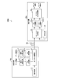
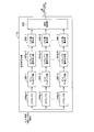
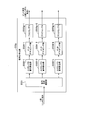
- FIG. 2 is a diagram showing a system configuration of the optical transmission system 100 according to the first embodiment.
- the optical transmission system 100 includes an optical transmitter 10 and an optical receiver 20.
- the optical transmitter 10 and the optical receiver 20 are connected via an optical fiber 30.
- the optical fiber 30 is a transmission line that connects the optical transmitter 10 and the optical receiver 20.
- the optical transmitter 10 includes a signal encoding unit 11, a DA converter 12, a signal light source 13, and an optical modulator 14.
- the data information input to the optical transmitter 10 is an M-value symbol before encoding.
- the signal encoding unit 11 converts an M-ary symbol string, which is data information, into an L-ary symbol string.
- the signal encoding unit 11 performs encoding by preferentially assigning an L-value symbol sequence having a small signal fluctuation to an M-value symbol sequence. As a result, it becomes possible to generate an L-value symbol string having a narrowed signal spectrum.
- the DA converter 12 converts the digital signal of the L-value symbol sequence generated by the signal encoding unit 11 into an analog signal.
- the DA converter 12 applies the analog signal to the optical modulator 14.
- the signal light source 13 sends out continuous light to the optical modulator 14.
- the optical modulator 14 modulates the continuous light emitted from the signal light source 13 with the analog signal applied by the DA converter 12 to generate an L-valued optical modulation signal.
- the optical modulator 14 transmits the generated L-valued optical modulation signal to the optical receiver 20 via the optical fiber 30.
- the signal light source 13 and the optical modulator 14 do not necessarily have to be separated, and the optical modulator 14 directly modulates the continuous light emitted from the signal light source 13 to generate an L-valued optical modulation signal. May be generated.
- the optical receiver 20 includes a light receiving unit 21, an AD converter 22, and a digital signal processing unit 23.
- the light receiving unit 21 directly detects the L-valued optical modulation signal transmitted from the optical transmitter 10, and acquires the light intensity information of the L-valued optical modulation signal.
- the light receiving unit 21 converts the acquired light intensity information into an analog electric signal and outputs the analog electric signal to the AD converter 22.
- the AD converter 22 converts the analog electric signal output from the light receiving unit 21 into a digital signal.
- the digital signal processing unit 23 acquires the M-value symbol before encoding by processing the digital signal.
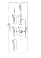
- FIG. 3 is a diagram showing an internal configuration of the digital signal processing unit 23 in the first embodiment.
- the digital signal processing unit 23 includes a digital filter 231, a signal determination unit 232, and a signal decoding unit 233.
- the digital filter 231 shapes the waveform of the L-valued optical modulation signal.
- the digital filter 231 outputs the L-valued optical modulation signal after waveform shaping to the signal determination unit 232.
- an FIR Finite Impulse Response
- the signal determination unit 232 acquires an L-value symbol sequence by performing symbol determination on the L-valued optical modulation signal after waveform shaping.
- the signal determination unit 232 outputs the acquired L-value symbol sequence to the signal decoding unit 233.
- the signal decoding unit 233 restores the M-value symbol sequence based on the correspondence between the L-value symbol sequence output from the signal determination unit 232 and the M-value symbol sequence.
- a correspondence table showing the correspondence relation between the L-value symbol sequence and the M-value symbol sequence may be transmitted from the optical transmitter 10 to the optical receiver 20 in advance. However, they may be transmitted together when the modulated signal is transmitted from the optical transmitter 10.
- an M-value symbol sequence is converted into an L-value symbol sequence having a larger value than the M value, and signal fluctuations in the converted L-value symbol sequence are reduced.
- Encoding is performed by extracting only such a pattern and allocating it so as to correspond to the M-ary symbol sequence at a ratio of 1: 1.
- the signal encoding unit 11 preferentially allocates the L-ary symbol sequence having a small signal fluctuation to the M-ary symbol sequence by performing the following procedures 1 to 6.
- the signal encoding unit 11 enumerates all L-valued symbol sequences composed of N + P symbols. As a result, L (N + P) L-value symbol strings are obtained.
- the signal encoding unit 11 obtains the signal spectrum of each L-value symbol string by performing a discrete Fourier transform on all L (N + P) L-value symbol strings.
- the signal encoding unit 11 calculates the spread of the signal spectrum of each L-ary symbol sequence.
- the signal encoding unit 11 performs (N + P) number series (F1, F2, ..., F (N + P ) obtained by performing a discrete Fourier transform on an L-value symbol sequence composed of (N + P) symbols. ) ) Is obtained, the signal spectrum broadening ⁇ 2 is obtained.
- This ⁇ 2 is the cost value.
- [] is a Gauss symbol.
- the signal encoding unit 11 sequentially assigns the L-value symbol sequence having the smallest cost value to the M-value symbol sequence.
- the value of the first symbol or the last symbol is limited to the L-value symbol sequence in which the value is [(L-1) / 2], and is assigned to the M-value symbol sequence. It is also possible to suppress high-frequency fluctuations at the boundary between consecutive symbol strings.
- the signal encoding unit 11 creates a correspondence table of the M-value symbol sequence that is the signal before encoding and the L-value symbol sequence that is the signal after encoding, based on the allocation result in procedure 4.
- the signal encoding unit 11 converts the M-ary symbol sequence into an L-ary symbol sequence based on the correspondence table. Thereby, the signal encoding unit 11 encodes the M-ary symbol sequence.
- the signal decoding unit 233 of the optical receiver 20 decodes the L-ary symbol sequence into the M-ary symbol sequence based on the correspondence table created above.
- FIG. 4 is a diagram showing signal spectra of binary symbols before coding and ternary symbols after coding obtained by the non-linear coding in the present invention.
- FIG. 4 (A) is a diagram showing a signal spectrum of a binary symbol before coding
- FIG. 4 (B) is a signal spectrum of a ternary symbol after coding obtained by the non-linear coding in the present invention. It is a figure.
- the horizontal axis represents frequency and the vertical axis represents signal power.
- a pseudo-random pattern of degree 15 is used as a binary symbol before encoding.
- a raised cosine filter with a roll-off coefficient of 0.01 is applied to the symbol sequence.
- FIG. 4 (B) in the coded symbol sequence, the generation of high frequency components is suppressed, and the signal power is concentrated in the low frequency region. That is, narrowing of the signal spectrum has been realized. This narrowing of the band reduces the effects of waveform limitation due to band limitation and chromatic dispersion inherent in the optical transmission system.
- FIG. 5 is a diagram showing an eye pattern of a received signal after being transmitted under a 10 GHz band limitation and a wavelength dispersion environment of ⁇ 64 ps / nm.
- 5A is a diagram showing the eye pattern in FIG. 4A
- FIG. 5B is a diagram showing the eye pattern in FIG. 4B.
- the modulation rate of the signal is 56 GBd
- waveform deterioration compensation by an 11-tap FIR (Finite Impulse Response) filter is applied to the received signal.
- FIR Finite Impulse Response
- FIG. 5 (A) in the binary symbol sequence before encoding, significant eye aperture deterioration occurs due to the influence of band limitation and chromatic dispersion, making it difficult to identify binary symbols. ing.
- FIG. 5 (B) in the ternary symbol sequence after encoding, a large eye opening deterioration does not occur even in an environment in which there is significant band limitation or chromatic dispersion, and the ternary symbol is It is in a state where it can be easily identified. That is, it can be confirmed that by applying the non-linear coding in the present invention, it is possible to improve the band limiting resistance and the chromatic dispersion resistance of the optical signal.
- FIG. 6 is a diagram showing a signal spectrum of a quaternary symbol before encoding and a quinary symbol after encoding obtained by nonlinear encoding in the present invention.
- FIG. 6 (A) is a diagram showing a signal spectrum of a 4-level symbol before coding
- FIG. 6 (B) is a signal spectrum of a 5-level symbol after coding obtained by the non-linear coding in the present invention. It is a figure.
- the horizontal axis represents frequency and the vertical axis represents signal power.
- no limitation is imposed on the first symbol and the last symbol with respect to the encoded four-valued symbol sequence.
- the generation of high frequency components is suppressed in the coded symbol sequence, and the signal power is concentrated in the low frequency region. That is, narrowing of the signal spectrum has been realized. This narrowing of the band reduces the effects of waveform limitation due to band limitation and chromatic dispersion inherent in the optical transmission system.
- FIG. 7 is a diagram showing an eye pattern of a reception signal after being transmitted under a 22 GHz band limitation and -32 ps / nm wavelength dispersion environment.
- FIG. 7A is a diagram showing the eye pattern in FIG. 6A
- FIG. 7B is a diagram showing the eye pattern in FIG. 6B.
- the modulation rate of the signal is 56 GBd
- the waveform deterioration compensation by the 31-tap FIR filter is applied to the received signal.
- the signal encoding unit 11 of the optical transmitter 10 performs the encoding process of the above steps 1 to 6 to perform the L-level symbol. It is possible to select a pattern that reduces the signal fluctuation in the columns. Then, the signal encoding unit 11 performs encoding so as to correspond to the selected L-value symbol sequence and the M-value symbol sequence in a 1: 1 relationship. By this means, it is possible to generate an L-ary symbol string having a narrowed signal spectrum. Therefore, it is possible to suppress deterioration of signal quality even in a situation where there is band limitation and to perform high-quality transmission.
- encoding is performed using a cost function different from the cost function shown in the second embodiment.
- the signal encoding unit 11 calculates the signal spectrum spread ⁇ 2 as the cost function in [Procedure 3] of the third embodiment by performing the calculations shown in the following Expressions 2 and 3 without using the signal spectrum. obtain.
- This ⁇ 2 is the cost value.
- the L-value symbol sequence composed of N symbols is (S1, S2, ..., S (N + P) ).
- the signal spectrum spread ⁇ 2 obtained in this way also has a characteristic that it exhibits a large value for a symbol sequence having a large signal variation and a small value for a symbol sequence having a small signal variation.
- ⁇ 2 32 for a ternary symbol sequence with large signal fluctuations such as 0202 and 2020, and a ternary symbol sequence with small signal fluctuations such as 0000, 1111 and 2222.
- ⁇ 2 0.
- the signal encoding unit 11 is limited to the L-value symbol string in which the value of the first symbol or the last symbol of the L-value symbol string is [(L ⁇ 1) / 2]. Then, by assigning it to the M-value symbol sequence, it is also possible to suppress high-frequency fluctuations at boundaries between temporally consecutive symbol sequences.
- the signal encoding unit 11 of the optical transmitter 10 performs an encoding process by a method different from that of the second embodiment. Specifically, the signal encoding unit 11 calculates the cost value representing the spread of the signal spectrum without using the signal spectrum. Then, the signal encoding unit 11 selects the L-value symbol sequence in order from the L-value symbol sequence having the smallest cost value based on the calculated cost value. Thereby, the signal coding unit 11 can select a pattern in the L-ary symbol sequence in which the signal fluctuation is small. Then, the signal encoding unit 11 performs encoding so as to correspond to the selected L-value symbol sequence and the M-value symbol sequence in a 1: 1 relationship. By this means, it is possible to generate an L-ary symbol string having a narrowed signal spectrum. Therefore, it is possible to suppress deterioration of signal quality even in a situation where there is band limitation and to perform high quality transmission.
- the signal coding unit 11 in the third embodiment performs coding without using the signal spectrum.
- the signal encoding unit 11 does not need to perform the discrete Fourier transform process on each L-ary symbol sequence. Therefore, [Procedure 2] in the second embodiment can be omitted. That is, the processing can be shortened as compared with the second embodiment.
- FIG. 8 is a diagram showing a system configuration of an optical transmission system 100a according to the fourth embodiment.
- the optical transmission system 100a includes an optical transmitter 10a and an optical receiver 20a.
- the optical transmitter 10a and the optical receiver 20a are connected via an optical fiber 30.
- the optical transmitter 10a includes signal encoders 11a-1 and 11a-2, DA converters 12a-1 and 12a-2, a signal light source 13, and an optical vector modulator 15.
- the signal encoding unit 11a-1 and the DA converter 12a-1 are functional units that process the data information I.
- the signal coding unit 11a-2 and the DA converter 12a-2 are functional units that process the data information Q.
- the data information I and Q are M-value symbols before encoding, and are sequences of independent M-value symbols.
- the signal coding units 11a-1 and 11a-2 will be referred to as the signal coding unit 11a if no distinction is made between them. Further, in the following description, the DA converters 12a-1 and 12a-2 will be referred to as the DA converters 12a unless they are distinguished from each other.
- the signal encoding unit 11a inputs data information I and Q to be transmitted from the outside, and converts the M-value symbol sequence corresponding to the input data information I and Q into an L-value symbol sequence. Specifically, the signal encoding unit 11a-1 converts the M-ary symbol sequence corresponding to the input data information I into an L-ary symbol sequence. The signal encoding unit 11a-2 converts the M-ary symbol sequence corresponding to the input data information Q into an L-ary symbol sequence. The signal encoding unit 11a performs encoding in which an L-value symbol sequence with a small signal fluctuation is preferentially assigned to an M-value symbol sequence. As a result, it becomes possible to generate an L-value symbol string having a narrowed signal spectrum.
- the DA converter 12a converts the digital signal of the L-value symbol sequence generated by the signal encoding unit 11a into an analog signal.
- the DA converter 12a applies an analog signal to the optical vector modulator 15.
- the DA converter 12a-1 converts the digital signal of the L-value symbol sequence generated by the signal encoding unit 11a-1 into an analog signal.
- the DA converter 12a-1 applies the analog signal to the optical vector modulator 15.
- the DA converter 12a-2 converts the digital signal of the L-value symbol sequence generated by the signal encoding unit 11a-2 into an analog signal.
- the DA converter 12a-2 applies the analog signal to the optical vector modulator 15.
- the signal light source 13 sends continuous light to the optical vector modulator 15.
- the optical vector modulator 15 independently performs amplitude modulation using the analog signals output from the DA converters 12a-1 and 12a-2. Specifically, the optical vector modulator 15 modulates the continuous light emitted from the signal light source 13 using an analog signal to generate an L 2 -QAM signal whose L value is in each of the I channel and the Q channel. To generate.
- the optical vector modulator 15 transmits the generated L 2 -QAM signal to the optical receiver 20a via the optical fiber 30.
- the optical receiver 20a includes AD converters 22a-1 and 22a-2, a digital signal processing unit 23a, a local light source 24, and a coherent receiver 25.
- the local light source 24 outputs local light that interferes with the received signal light.
- the coherent receiver 25 converts the L 2 -QAM signal into an analog electric signal by coherently detecting the L 2 -QAM signal transmitted from the optical transmitter 10a based on the local light.
- the AD converter 22a converts the analog electric signal output from the coherent receiver 25 into a digital signal. Specifically, the AD converter 22a-1 converts the analog electric signal of the I component into a digital signal. The AD converter 22a-2 converts the Q component analog electric signal into a digital signal. The digital signal processing unit 23a processes the digital signal to obtain M-value symbols before encoding corresponding to the data information I and the data information Q, respectively.
- FIG. 9 is a diagram showing the internal configuration of the digital signal processing unit 23a in the fourth embodiment.
- the digital signal processing unit 23a includes a digital filter 231a, signal determination units 232a-1 and 232a-2, signal decoding units 233a-1 and 233a-2, an IQ synthesis unit 234, and an IQ separation unit 235.
- the IQ synthesizing unit 234 takes in each of the digital signals output from the AD converters 22a-1 and 22a-2 as a real part (digital signal of I channel component) and an imaginary part (digital signal of Q channel component).
- the IQ combiner 234 combines the captured signals into a complex signal.
- the IQ synthesizer 234 takes in the digital signal output from the AD converter 22a-1 as a real part and the digital signal output from the AD converter 22a-2 as an imaginary part, and takes in each signal. Is synthesized as a complex signal.
- the digital filter 231a shapes the waveform of the signal that is complex-synthesized by the IQ synthesizer 234.
- the digital filter 231a outputs the complex-combined signal after waveform shaping to the IQ separation unit 235.
- the IQ separation unit 235 separates the signal output from the digital filter 231a into a real part (digital signal of I channel component) and an imaginary part (digital signal of Q channel component).
- the IQ separation unit 235 outputs the signal of the I channel component to the signal determination unit 232a-1, and outputs the signal of the Q channel component to the signal determination unit 232a-2.
- the signal determination unit 232a independently performs symbol determination on each of the I-channel component signal and the Q-channel component signal output from the IQ separation unit 235, so that the L value corresponding to the I-channel component and the Q-channel component is determined. Get each symbol string. Specifically, the signal determination unit 232a-1 acquires the L-value symbol sequence corresponding to the I channel component by performing symbol determination on the signal of the I channel component output from the IQ separation unit 235. The signal determination unit 232a-1 outputs the L value symbol sequence corresponding to the acquired I channel component to the signal decoding unit 233a-1. The signal determination unit 232a-2 acquires the L-value symbol sequence corresponding to the Q channel component by performing symbol determination on the signal of the Q channel component output from the IQ separation unit 235. The signal determination unit 232a-2 outputs the L value symbol sequence corresponding to the acquired Q channel component to the signal decoding unit 233a-2.
- the signal decoding unit 233a uses the data information output from the signal determining unit 232a based on the correspondence relationship between the L-value symbol sequence corresponding to the I-channel component and the L-value symbol sequence corresponding to the Q-channel component and the M-value symbol sequence.
- the M-ary symbol strings corresponding to I and Q are restored respectively.
- the signal decoding unit 233a-1 is based on the correspondence relationship between the L value symbol sequence corresponding to the I channel component output from the signal determining unit 232a-1 and the M value symbol sequence corresponding to the I channel component. Then, the M-ary symbol sequence corresponding to the data information I is restored.
- the signal decoding unit 233a-2 receives the data information Q based on the correspondence relationship between the L-value symbol sequence corresponding to the Q channel component output from the signal determining unit 232a-2 and the M-value symbol sequence corresponding to the Q channel component. The M-ary symbol sequence corresponding to is restored.
- the L value symbol sequence corresponding to the I channel component and the M value symbol sequence corresponding to the I channel component are The correspondence table indicating the correspondence may be transmitted from the optical transmitter 10a to the optical receiver 20a in advance, or may be transmitted together when the modulated signal is transmitted from the optical transmitter 10a.
- the correspondence table showing the correspondence relationship between the columns may be transmitted from the optical transmitter 10a to the optical receiver 20a in advance, or may be transmitted together when the modulated signal is transmitted from the optical transmitter 10a.
- the optical transmission system 100a configured as described above can be applied to QAM signals.
- FEC Forward error correction
- a configuration in which error correction is applied to a PAM signal will be described.
- the optical transmitter performs non-linear coding and then error correction coding
- the optical receiver performs error correction decoding and then non-linear decoding.
- the error correction code may be an error correction code based on hard decision information or an error correction code based on soft decision information.
- FIG. 10 is a diagram showing a system configuration of an optical transmission system 100b according to the fifth embodiment.
- the optical transmission system 100b includes an optical transmitter 10b and an optical receiver 20b.
- the optical transmitter 10b and the optical receiver 20b are connected via an optical fiber 30.
- the optical fiber 30 is a transmission line that connects the optical transmitter 10b and the optical receiver 20b.
- the optical transmitter 10b includes a signal encoder 11, a DA converter 12b, a signal light source 13, an optical modulator 14, and an error correction encoder 16.
- the data information input to the optical transmitter 10b is an M-value symbol before encoding.
- the optical transmitter 10b performs the same processing as that of the optical transmitter 10 in any of the first to third embodiments, except for the configuration of the DA converter 12b and the error correction coding unit 16. Only the differences will be described below.
- the error correction coding unit 16 performs error correction coding on the digital signal of the L-ary symbol sequence generated by the signal coding unit 11.
- the error correction coding unit 16 outputs the digital signal of the L value symbol string after the error correction coding to the DA converter 12b.
- the DA converter 12b converts the digital signal of the L value symbol string after the error correction coding output from the error correction coding unit 16 into an analog signal.
- the DA converter 12b applies an analog signal to the optical modulator 14.
- the optical receiver 20b includes a light receiving unit 21, an AD converter 22, and a digital signal processing unit 23b.
- the optical receiver 20b performs the same processing as that of the optical receiver 20 in any of the first to third embodiments, except for the configuration of the digital signal processing unit 23b. Only the differences will be described below.
- the digital signal processing unit 23b acquires the M-value symbol before encoding by processing the digital signal.
- FIG. 11 is a diagram showing an internal configuration of the digital signal processing unit 23b in the fifth embodiment.
- the digital signal processing unit 23b includes a digital filter 231, a signal determination unit 232, a signal decoding unit 233b, and an error correction decoding unit 236.
- the configurations of the digital filter 231 and the signal determination unit 232 perform the same processing as that of the functional unit having the same name in any of the first to third embodiments, and thus the description thereof will be omitted.
- the error correction decoding unit 236 performs error correction decoding on the L-value symbol sequence output from the signal determination unit 232.
- the error correction decoding unit 236 outputs the digital signal of the L-value symbol sequence after error correction decoding to the signal decoding unit 233b.
- the signal decoding unit 233b restores the M-value symbol sequence based on the correspondence relationship between the error-correction-decoded L-value symbol sequence output from the error-correction decoding unit 236 and the M-value symbol sequence.
- error correction coding is performed after performing nonlinear coding in the optical transmitter 10b. Then, the optical receiver 20b performs error correction decoding and then nonlinear decoding. By performing such processing, it is possible to sufficiently reduce the symbol error with respect to the L-ary symbol generated by the transmission and then perform the non-linear decoding. Therefore, it is possible to avoid continuous errors due to the non-linear block coding.
- FIG. 12 is a diagram showing a system configuration of an optical transmission system 100c in the sixth embodiment.
- the optical transmission system 100c includes an optical transmitter 10c and an optical receiver 20c.
- the optical transmitter 10c and the optical receiver 20c are connected via an optical fiber 30.
- the optical fiber 30 is a transmission line that connects the optical transmitter 10c and the optical receiver 20c.
- the optical transmitter 10c includes signal coding units 11a-1 and 11a-2, DA converters 12c-1 and 12c-2, a signal light source 13, an optical vector modulator 15, and error correction coding units 16c-1 and 16c-. 2 is provided. Regarding the configuration of the optical transmitter 10c other than the DA converters 12c-1 and 12c-2 and the error correction coding units 16c-1 and 16c-2, the same processing as that of the optical transmitter 10a in the fourth embodiment is performed. To do. Only the differences will be described below.
- the error correction coding unit 16c performs error correction coding on the digital signal of the L-value symbol sequence generated by the signal coding unit 11a. Specifically, the error correction coding unit 16c-1 performs error correction coding on the digital signal of the L-ary symbol sequence generated by the signal coding unit 11a-1. The error correction coding unit 16c-1 outputs the digital signal of the L value symbol sequence after the error correction coding to the DA converter 12c-1. The error correction coding unit 16c-2 performs error correction coding on the digital signal of the L-value symbol sequence generated by the signal coding unit 11a-2. The error correction coding unit 16c-2 outputs the digital signal of the L value symbol string after the error correction coding to the DA converter 12c-2.
- the DA converter 12c converts the digital signal of the L value symbol string after error correction coding output from the error correction coding unit 16c into an analog signal.
- the DA converter 12c applies an analog signal to the optical vector modulator 15.
- the DA converter 12c-1 converts the digital signal of the L value symbol string after error correction coding output from the error correction coding unit 16c-1 into an analog signal.
- the DA converter 12c-1 applies the analog signal to the optical vector modulator 15.
- the DA converter 12c-2 converts the digital signal of the L value symbol string after the error correction coding output from the error correction coding unit 16c-2 into an analog signal.
- the DA converter 12c-2 applies the analog signal to the optical vector modulator 15.
- the optical receiver 20c includes AD converters 22a-1 and 22a-2, a digital signal processing unit 23c, a local light source 24, and a coherent receiver 25.
- the optical receiver 20c performs the same processing as that of the optical receiver 20a in the fourth embodiment except for the configuration other than the digital signal processing unit 23c. Only the differences will be described below.
- the digital signal processing unit 23c processes the digital signal to obtain pre-encoding M-value symbols corresponding to the data information I and the data information Q.
- FIG. 13 is a diagram showing an internal configuration of the digital signal processing unit 23c in the sixth embodiment.
- the digital signal processing unit 23c includes a digital filter 231a, signal determination units 232a-1 and 232a-2, signal decoding units 233c-1 and 233c-2, an IQ combining unit 234, an IQ separation unit 235, and an error correction decoding unit 236-1.
- An error correction decoding unit 236-2 is provided.
- the configurations of the digital filter 231a, the signal determining units 232a-1 and 232a-2, the IQ synthesizing unit 234, and the IQ separating unit 235 are similar to those of the functional units having the same names in the fourth embodiment. The description is omitted because it is performed.
- the error correction decoding unit 236 performs error correction decoding on the L-value symbol sequence output from the signal determination unit 232a. Specifically, the error correction decoding unit 236-1 performs error correction decoding on the L-value symbol sequence output from the signal determination unit 232a-1. The error correction decoding unit 236-1 outputs the digital signal of the L value symbol sequence after the error correction decoding to the signal decoding unit 233c-1. The error correction decoding unit 236-2 performs error correction decoding on the L-ary symbol sequence output from the signal determination unit 232a-2. The error correction decoding unit 236-2 outputs the digital signal of the L value symbol sequence after the error correction decoding to the signal decoding unit 233c-2.
- the signal decoding unit 233c receives the data information based on the correspondence relationship between the L value symbol sequence corresponding to the I channel component and the L value symbol sequence corresponding to the Q channel component output from the signal determining unit 232a and the M value symbol sequence.
- the M-ary symbol strings corresponding to I and Q are restored respectively.
- the signal decoding unit 233c-1 includes an L-value symbol sequence after error correction decoding corresponding to the I channel component output from the error correction decoding unit 236-1 and an M value symbol corresponding to the I channel component.
- the M-value symbol sequence corresponding to the data information I is restored based on the column correspondence.
- the signal decoding unit 233c-2 determines the correspondence relationship between the L-value symbol sequence after error correction decoding corresponding to the Q channel component output from the error correction decoding unit 236-2 and the M-value symbol sequence corresponding to the Q channel component. Based on this, the M-ary symbol string corresponding to the data information Q is restored.
- error correction coding is performed after performing nonlinear coding in the optical transmitter 10c. Then, the optical receiver 20c performs error correction decoding and then nonlinear decoding. By performing such processing, it is possible to sufficiently reduce the symbol error with respect to the L-ary symbol generated by the transmission and then perform the non-linear decoding. Therefore, even when the QAM signal is used, it is possible to avoid continuous errors caused by the non-linear block coding.
- FIG. 14 is a diagram showing the internal configuration of the digital signal processing unit 23d in the seventh embodiment.
- the digital signal processing unit 23d includes a signal decoding unit 233d, a first digital filter 237, a Viterbi decoding unit 238, a second digital filter 239, an adder 240, and a metric calculation unit 241.
- the first digital filter 237 shapes the waveform of the L-valued optical modulation signal.
- the first digital filter 237 is used to compensate for waveform deterioration of the L-ary symbol sequence.
- the first digital filter 237 outputs the L-valued optical modulation signal after waveform shaping to the Viterbi decoding unit 238 and the adder 240.
- a general linear filter such as an FIR filter or a Volterra filter is used.
- the Viterbi decoding unit 238 performs sequence estimation based on the L-valued optical modulation signal output from the first digital filter 237 and the metric output from the metric calculation unit 241.
- a Viterbi algorithm is a typical algorithm for making a determination based on a metric value.
- the Viterbi decoding unit 238 performs sequence estimation based on the Viterbi algorithm, and employs the symbol sequence with the smallest metric among the metrics obtained as a result of sequence estimation as the transmission sequence.
- the second digital filter 239 acquires time-series data by performing digital filter processing on the input candidate series.
- the candidate sequence is an L-value symbol sequence used when performing MLSE.
- the second digital filter 239 is for simulating the waveform deterioration that occurs in the transmission path for the L-value symbol sequence that is the candidate sequence.
- the second digital filter 239 outputs the acquired time series data to the adder 240.
- a general linear filter such as an FIR filter or a Volterra filter is used.
- a Volterra filter may be used as the second digital filter 239.
- the adder 240 takes in the value output from the first digital filter 237 and the value output from the second digital filter 239.
- the adder 240 takes in the value output from the second digital filter 239 with a minus sign.
- the adder 240 adds the two captured values, that is, subtracts the value (time series data) output from the second digital filter 239 from the value (time series data) output from the first digital filter 237,
- the subtraction value calculated by the subtraction is output to the metric calculation unit 241.
- the metric calculator 241 performs time-series data obtained by digitally filtering the subtraction value output from the adder 240, that is, an assumed sequence candidate (candidate sequence) by the second digital filter 239, and the first digital.
- the Euclidean distance from the time series data output from the filter is calculated as a metric.
- the signal decoding unit 233d restores the M-ary symbol sequence based on the correspondence between the transmission symbol sequence output from the Viterbi decoding unit 238 and the M-ary symbol sequence.
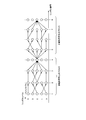
- FIG. 15 is a diagram showing an image of the trellis diagram when the end point value is fixed.
- the trellis path converges to one point at the block end point (symbol numbers 4 and 8 in FIG. 15), it is possible to determine the four symbols constituting the block for each block. , The symbol determination result in that block does not affect the symbol determination in other blocks.
- the maximum likelihood sequence estimation is applied to the PAM signal for processing.
- the L-value symbol sequence to be subjected to the non-linear coding is regarded as one block, that is, the L-value symbol sequence composed of (N + P) symbols. Can be regarded as one block, and sequence estimation can be applied.
- the trellis line in MLSE Since the start point and the end point in the figure are fixed, the maximum likelihood sequence estimation can be performed for each block, and the delay associated with symbol determination can be minimized.
- the optical transmitter 10 includes the error correction coding unit 16, and the digital signal processing unit 23d includes the error correction decoding unit 236.
- FIG. 16 is a diagram showing an internal configuration of the digital signal processing unit 23e in the eighth embodiment.
- the digital signal processing unit 23e includes signal decoding units 233e-1 and 233e-2, IQ combining unit 234, IQ separating unit 235e, first digital filter 237e, Viterbi decoding units 238e-1 and 238e-2, second digital filter 239e. , Adders 240e-1 and 240e-2, metric calculating units 241e-1 and 241e-2, a phase estimating unit 242, an IQ combining unit 243, and an IQ separating unit 244.
- the IQ synthesizing unit 234 takes in each digital signal output from the AD converters 22a-1 and 22a-2 as a real part (digital signal of I channel component) and an imaginary part (digital signal of Q channel component).
- the IQ combiner 234 combines the captured signals into a complex signal. Specifically, the IQ synthesizer 234 takes in the digital signal output from the AD converter 22a-1 as a real part and the digital signal output from the AD converter 22a-2 as an imaginary part, and takes in each signal. Is synthesized as a complex signal.
- the first digital filter 237e shapes the waveform of the L-valued optical modulation signal.
- the first digital filter 237e is used to compensate for waveform deterioration of the L-ary symbol sequence.
- the first digital filter 237e outputs the L-valued optical modulation signal after waveform shaping to the phase estimation unit 242.
- a general linear filter such as an FIR filter or a Volterra filter is used.
- the phase estimation unit 242 compensates for the phase difference between the signal light and the local oscillation light by the local oscillation light source 24.
- Phase estimation section 242 outputs the compensated signal to IQ separation section 235.
- the IQ separation unit 235e separates the signal output from the phase estimation unit 242 into a real part (I channel component) and an imaginary part (Q channel component).
- the IQ separation unit 235e outputs the signal of the I channel component to the Viterbi decoding unit 238e-1 and the adder 240e-2, and outputs the signal of the Q channel component to the Viterbi decoding unit 238e-2 and the adder 240e-1.
- the Viterbi decoding unit 238e uses the signal corresponding to the real part (I channel component) and the signal corresponding to the imaginary part (Q channel component) output from the IQ separation unit 235e and the metric output from the metric calculation unit 241e. Based on this, sequence estimation is performed based on each. Specifically, the Viterbi decoding unit 238e-1 performs sequence estimation on the I channel component based on the signal corresponding to the real part (I channel component) and the metric based on the Viterbi algorithm. The Viterbi decoding unit 238e-1 employs the symbol sequence having the smallest metric among the metrics obtained as a result of sequence estimation as the transmission sequence in the I channel component.
- the Viterbi decoding unit 238e-2 performs sequence estimation on the Q channel component based on the signal corresponding to the imaginary part (Q channel component) and the metric based on the Viterbi algorithm.
- the Viterbi decoding unit 238e-2 adopts the symbol sequence having the smallest metric among the metrics obtained as a result of sequence estimation as the transmission sequence in the Q channel component.
- IQ synthesizing section 243 synthesizes each of the input candidate sequence for the I channel component and the candidate sequence for the Q channel component into a complex number.
- the candidate sequences in this embodiment are an L-value symbol sequence for the I channel component and an L-value symbol sequence for the Q channel component used when performing MLSE.
- the second digital filter 239e acquires time series data by performing digital filter processing on the candidate series combined by the IQ combining unit 243.
- the second digital filter 239e is for simulating the waveform deterioration that occurs in the transmission path for the L-ary symbol sequence that is the candidate sequence.
- the second digital filter 239e outputs the acquired time series data to the IQ separation unit 244.
- a general linear filter such as an FIR filter or a Volterra filter is used.
- a Volterra filter may be used as the second digital filter 239e.
- the IQ separation unit 244 separates the signal of the time series data output from the second digital filter 239e into a real part (I channel component) and an imaginary part (Q channel component).
- the IQ separation unit 244 outputs the signal of the I channel component to the adder 240-1 and the signal of the Q channel component to the adder 240e-2.
- the adder 240e-1 captures the value (Q channel component signal) output from the IQ separation unit 235e and the value (Q channel component signal) output from the IQ separation unit 244.
- the adder 240e-1 takes in the value output from the IQ separation unit 235e with a minus sign.
- the adder 240e-1 adds the two captured values, that is, subtracts the value output from the IQ separation section 235e from the value output from the IQ separation section 244, and subtracts the subtraction value calculated by the subtraction from the metric calculation section. It is output to 241e-1.
- the adder 240e-2 takes in the value output from the IQ separation unit 235e (I channel component signal) and the value output from the IQ separation unit 244 (I channel component signal).
- the adder 240e-2 takes in the value output from the IQ separation unit 235e with a minus sign.
- the adder 240e-2 adds the two captured values, that is, subtracts the value output from the IQ separation unit 235e from the value output from the IQ separation unit 244, and subtracts the subtraction value calculated by the subtraction from the metric calculation unit. It is output to 241e-2.
- the metric calculator 241e-1 calculates the subtraction value output from the adder 240e-1 as a metric.
- the metric calculator 241e-2 calculates the subtraction value output from the adder 240e-2 as a metric.
- the signal decoding unit 233e outputs the data information based on the correspondence relationship between the L-value symbol sequence corresponding to the I-channel component and the L-value symbol sequence corresponding to the Q-channel component output from the Viterbi decoding unit 238e, and the M-value symbol sequence.
- the M-ary symbol strings corresponding to I and Q are restored respectively.
- the signal decoding unit 233e-1 is based on the correspondence relationship between the L value symbol sequence corresponding to the I channel component output from the Viterbi decoding unit 238e-1 and the M value symbol sequence corresponding to the I channel component. Then, the M-ary symbol sequence corresponding to the data information I is restored.
- the signal decoding unit 233e-2 is based on the correspondence relationship between the L-value symbol sequence after error correction decoding corresponding to the Q channel component output from the Viterbi decoding unit 238-2 and the M-value symbol sequence corresponding to the Q channel component. Then, the M-ary symbol string corresponding to the data information Q is restored.
- the maximum likelihood sequence estimation is applied to the QAM signal to perform processing.
- MLSE is a method corresponding to the determination for the entire sequence
- the L-value symbol sequence to be subjected to the non-linear coding is regarded as one block, that is, the L-value symbol sequence composed of (N + P) symbols.
- sequence estimation can be applied.
- the trellis line in MLSE Since the start point and the end point in the figure are fixed, the maximum likelihood sequence estimation can be performed for each block, and the delay associated with symbol determination can be minimized.
- the configuration using maximum likelihood sequence estimation has been described in the fourth embodiment, but the configuration shown in the present embodiment can also be applied to the sixth embodiment.
- the optical transmitter 10c includes error correction coding units 16c-1 and 16c-2
- the digital signal processing unit 23e includes 236-1 and 236-2.
- the cost value ⁇ 2 is calculated for all L (N + P) symbol strings that can be candidates as the L-value symbol string after nonlinear coding, and the cost value is small.
- the L-value symbol sequences are assigned 1: 1 to the M-value symbol sequences, which are the symbols before encoding, in order from the first one.
- a method of executing non-linear coding by calculating cost values for a small number of candidates will be described.
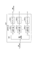
- FIG. 17 is a diagram showing an internal configuration of the signal encoding unit 11f in the ninth embodiment.
- the signal encoding unit 11f includes scramblers 246-1 to 246-k (k is an integer of 2 or more), scrambler number assigning units 247-1 to 247-k, cost value calculating units 248-1 to 248-k, and
- the sequence selection unit 249 is provided. Also in the present embodiment, it is assumed that one block of the M-ary symbol string to which the non-linear coding is applied is composed of N M-ary symbols.
- the scrambler 246-1 to 246-k will be referred to as the scrambler 246 if no distinction is made.
- the scrambler number assigning units 247-1 to 247-k will be referred to as the scrambler number assigning unit 247 if no distinction is made.
- the cost value calculation units 248-1 to 248-k will be referred to as the cost value calculation unit 248 if no distinction is made.
- the scrambler 246 converts the M-ary symbol sequence that is a symbol sequence before encoding into an L-ary symbol sequence composed of N + P ⁇ 1 L-ary symbols.
- the scramble processing executed by each of the scramblers 246-1 to 246-k is reversible conversion, and each scrambler executes reversible conversion based on different conversion rules.
- different K types of L-value symbol sequences are generated.
- An example of the reversible transformation by the scrambler 246 is a (N + P-1) ⁇ N matrix having a pseudo-inverse matrix.
- the scrambler number assigning unit 247 assigns a symbol indicating a scrambler number to each of the K types of L-value symbol strings.
- the cost value calculation unit 248 calculates the cost value for each of the L-value symbol strings each composed of (N + P) L symbols.
- the sequence selection unit 249 selects the sequence with the smallest cost value from the K types of L-value symbol sequences. The sequence selection unit 249 outputs the selected sequence as an output of the signal encoding unit 11f.
- FIG. 18 is a diagram showing an internal configuration of the signal decoding unit 233f in the ninth embodiment.
- the signal decoding unit 233f includes a decoding sequence selection unit 2331, scrambler number removal units 2332-1 to 2332-k, and descramblers 2333-1 to 2333-k.
- the scrambler number removing units 2332-1 to 2332-k will be referred to as the scrambler number removing unit 2332 if no distinction is made.
- the descramblers 2333-1 to 2333-k will be referred to as the descrambler 2333 if no distinction is made.
- the decoding sequence selection unit 2331 selects the output destination of the received L-value symbol sequence. Specifically, first, decoding sequence selecting section 2331 confirms the symbol indicating the scrambler number given to the L-ary symbol sequence. Next, as a result of the confirmation, the decoding sequence selection unit 2331 identifies which of the K types of scramblers has encoded the L-value symbol sequence. Then, decoding sequence selecting section 2331 outputs the L-value symbol sequence to scrambler number removing section 2332 corresponding to the L-value symbol sequence based on the identification result.
- the scrambler number removing unit 2332 removes the symbol indicating the scrambler number from the L-value symbol sequence.
- the scrambler number removing unit 2332 outputs the L-value symbol sequence after removing the symbol indicating the scrambler number to the descrambler 2333.
- the descrambler 2333 uses the descrambler corresponding to the scrambler number confirmed by the decoding sequence selection unit 2331 to execute the decoding process corresponding to the inverse conversion of the encoding process by the scrambler, and to execute the symbol before coding. A series of M-ary symbol sequences is restored.
- An example of the reversible transformation by the scrambler 246 is a (N + P-1) ⁇ N matrix having a pseudo inverse matrix.
- Block coding using such a matrix is reversible coding, and decoding can be realized by causing the descrambler 2333 to act on a pseudo-inverse matrix. Therefore, by using K different (N + P-1) ⁇ N matrices having pseudo-inverse matrices as the K types of scrambler, the encoding process and the decoding process in the present embodiment can be executed.
- the coded symbol sequence is composed of L-valued symbols, and therefore the calculation of the sum associated with the matrix calculation is an operation modulo L-1.
- the signal encoding unit 11f extracts an M-ary symbol sequence, which is a symbol sequence before encoding, from N + P ⁇ 1 L-ary symbols. Convert to a constructed L-value symbol string. As described above, the signal encoding unit 11f does not need to calculate the cost value ⁇ 2 for all L (N + P) symbol sequences that can be candidates as the L-value symbol sequence after nonlinear encoding in the signal encoding unit 11f. Therefore, the amount of calculation can be reduced.
- J is an integer of 1 or more bits.
- the J bits are assigned to the L-value symbol string composed of N symbols.
- 2 J pieces are extracted in order from the L-value symbol string having the smallest cost value as shown in the second and third embodiments.
- the L value symbol string is assigned to the J bits in a ratio of 1: 1.
- FIG. 19 is a diagram showing an internal configuration of the signal encoding unit 11g in the tenth embodiment.
- the signal encoding unit 11g includes scramblers 246g-1 to 246g-k, scrambler numbering units 247g-1 to 247g-k, cost value calculation units 248-1 to 248-k, a sequence selection unit 249, and a bit mapping unit. 250-1 to 250-k.
- the scrambler 246g-1 to 246g-k will be referred to as the scrambler 246g if no distinction is made.
- the scrambler number assigning units 247g-1 to 247g-k will be referred to as the scrambler number assigning unit 247g if no distinction is made.
- the bit mapping units 250-1 to 250-k will be referred to as the bit mapping unit 250 if no distinction is made.
- the scrambler 246g receives as an input a binary symbol sequence that is a symbol sequence before encoding.
- a binary symbol sequence (bit sequence) that is a symbol sequence before encoding is subjected to different scrambling processing in each scrambler 246g-1 to 246g-k.
- the scramble processing executed by each of the scramblers 246g-1 to 246g-k is a linear conversion that changes the order of the bits of the binary symbol string composed of J bits. .About.246g-k perform linear transformation based on different interchange rules. As a result, different K-type bit sequences composed of J bits are generated.
- the bit mapping unit 250 converts each bit sequence into an L-value symbol string composed of N ⁇ H L-value symbols.
- the scrambler number assigning unit 247g assigns a symbol indicating a scrambler number to each of the K types of L-value symbol sequences converted by the bit mapping unit 250.
- the symbol indicating the scrambler number is represented using H L-value symbols. By doing so, K-type different L-value symbol sequences composed of N L-value symbols are generated.
- FIG. 20 is a diagram showing the internal configuration of the signal decoding unit 233g in the tenth embodiment.
- the signal decoding unit 233g includes a decoding sequence selection unit 2331, scrambler number removal units 2332-1 to 2332-k, descramblers 2333g-1 to 2333g-k, and bit demapping units 2334-1 to 2334-k.
- bit demapping unit 2334 if the descramblers 2333g-1 to 2333g-k are not distinguished, they will be referred to as descrambler 2333g. Further, in the following description, the bit demapping units 2334-1 to 2334-k will be referred to as the bit demapping unit 2334 if no distinction is made.
- the bit demapping unit 2334 performs demapping processing on each L value symbol string.
- the descrambler 2333g uses the descrambler corresponding to the scrambler number confirmed by the decoding sequence selection unit 2331 to execute the decoding process corresponding to the inverse conversion of the encoding process by the scrambler, and to perform the decoding process on the symbol before encoding. A binary symbol sequence that is a sequence is restored.
- Each matrix is a unit matrix and an arbitrary row of the unit matrix is replaced multiple times.
- A represents a matrix operated by the scrambler 246g. For example, assuming that the bit string before encoding is [10010111], the output from each scrambler 246g is as follows.
- Output from scrambler 246g-1 [10010111]
- Output from scrambler 246g-2 [00101111]
- Output from scrambler 246g-3 [01011110]
- the conventional Gray code is applied as the bit mapping executed by the bit mapping unit 250. For example, the allocation “00 ⁇ 0, 01 ⁇ 1, 11 ⁇ 2, 10 ⁇ 3” is performed. By applying such a bit mapping, a 4-level symbol sequence composed of 4 symbols is generated.
- the four-level symbol string corresponding to each scrambler 246g is as follows.
- bit string can be restored from a quaternary symbol string by converting a quaternary symbol into 2 bits based on the Gray code.
- a scrambler number is assigned to the 4-level symbol string output from the bit mapping. For example, the symbol corresponding to the scrambler number is added to the end of the quaternary symbol.
- the symbol to give
- the outputs from the scrambler numbering units 247g-1 to 247g-k are as follows.
- Output corresponding to scrambler 246g-1 2031122
- Output corresponding to scrambler 246g-2 21032222
- Output corresponding to scrambler 246g-3 22112232
- Output corresponding to scrambler 246g-4 2323112
- the cost value calculation unit 248 calculates a cost value for each of these four-valued symbol strings. If the cost value shown in Equation 2 is used as the cost value, the cost value of the output corresponding to each scrambler 246g is as follows, and the output from the scrambler 246g-3 is the 4-value symbol sequence with the smallest cost value. It can be seen that it is. Therefore, it can be concluded that the output corresponding to the scrambler 246g-3 is a quaternary symbol sequence with the smallest signal fluctuation.
- the sequence selection unit selects the output corresponding to the scrambler 246g-3, that is, [22111232] as the 4-level symbol sequence to be transmitted.
- Output cost value corresponding to scrambler 246g-1 56
- Output cost value corresponding to scrambler 246g-2 33
- Output cost value corresponding to scrambler 246g-3 7
- the signal decoding unit 233g of the optical receiver 20 confirms the scrambler number assigned to the 4-level symbol sequence.
- the scrambler number is 3 from the value "2" of the second symbol.
- the scrambler number removing unit 2332 removes the first two symbols and the last one symbol assigned by the scrambler number assigning unit 247g.
- the 4-valued symbol string obtained by this is [1123].
- the bit demapping unit 2334 converts the quaternary symbol into a binary symbol based on the Gray code. As a result, an 8-bit string [0101110] is obtained.
- a descrambler 2333g-3 applies the matrix of the following equation 8 corresponding to the transposed matrix of the matrix operated by the scrambler 246g-3 to the bit string, which is the bit string before encoding [10010111].
- 21 (A) and 22 (A) are diagrams showing a signal spectrum of a 4-level symbol before encoding
- FIGS. 21 (B) and 22 (B) are obtained by the non-linear encoding in the present invention. It is a figure which shows the signal spectrum of the quaternary symbol after encoding. 21 and 22, the horizontal axis represents frequency and the vertical axis represents signal power.
- Equation 1 is used to calculate the cost value in FIG. 21, and Equation 2 is used to calculate the cost value in FIG.
- the generation of high frequency components is suppressed in the coded symbol sequence, and the signal power is concentrated in the low frequency region. That is, narrowing of the signal spectrum has been realized. This narrowing of the band reduces the effects of waveform limitation due to band limitation and chromatic dispersion inherent in the optical transmission system.
- optical transmission system 100 of the ninth embodiment configured as described above, it is possible to generate an L-value symbol sequence from a bit sequence. As a result, the processing in each of the above-described embodiments can be performed even when the data information is input as a bit sequence.
- a part or all of the functions of the optical transmitters 10, 10a, 10b, 10c and the optical receivers 20, 20a, 20b, 20c in the above-described embodiments may be realized by a computer.
- the program for realizing this function may be recorded in a computer-readable recording medium, and the program recorded in this recording medium may be read by a computer system and executed.
- the “computer system” mentioned here includes an OS and hardware such as peripheral devices.
- the “computer-readable recording medium” refers to a portable medium such as a flexible disk, a magneto-optical disk, a ROM, a CD-ROM, or a storage device such as a hard disk built in a computer system.
- the "computer-readable recording medium” means to hold a program dynamically for a short time like a communication line when transmitting the program through a network such as the Internet or a communication line such as a telephone line.
- a network such as the Internet or a communication line such as a telephone line.
- the program may be for realizing some of the functions described above, or may be one that can realize the functions described above in combination with a program already recorded in the computer system, It may be realized using a programmable logic device such as FPGA (Field Programmable Gate Array).
- Digital filter 232, 232a, 232a-1, 232a-2 ...
- Signal determination unit 233, 233a-1, 233a-2, 233b, 233c-1, 233c 2, 233d, 233e-1, 233e-2, 233f, 233g ...
- Signal decoding unit 2331 ...
- Decoding sequence selection unit 2332-1-2332-k ... Scrambler number removing unit, 2333-1-2333-k, 2333g -1 to 2333g-k ... descrambler, 2334-1 to 2334-k ... bit demapping section, 234 ... IQ combining section, 235, 235e ... IQ separating section, 236, 236a-1, 236a-2 ...
- error correction decoding Section 237, 237e ... first digital filter, 238, 238e-1, 238e-2 ... Viterbi decoding section, 239, 239e ... second digital filter, 240, 240e-1, 240e-2 ... adder, 241, 241e -1, 241e-2 ... Metric calculation unit, 242 ... Phase estimation unit, 243 ... Q synthesis section, 244 ... IQ separation section, 246-1 to 246-k, 246g-1 to 246g-k ... scrambler, 247-1 to 247-k, 247g-1 to 247g-k ... scrambler numbering section , 248-1 to 248-k ... Cost value calculation unit, 249 ... Sequence selection unit, 250-1 to 250-k ... Bit mapping unit
Landscapes
- Engineering & Computer Science (AREA)
- Physics & Mathematics (AREA)
- Computer Networks & Wireless Communication (AREA)
- Signal Processing (AREA)
- Electromagnetism (AREA)
- Probability & Statistics with Applications (AREA)
- Theoretical Computer Science (AREA)
- Spectroscopy & Molecular Physics (AREA)
- Optical Communication System (AREA)
- Dc Digital Transmission (AREA)
- Error Detection And Correction (AREA)
- Detection And Prevention Of Errors In Transmission (AREA)
Abstract
光送信器と、光受信器とを備える光伝送システムであって、光送信器は、データ情報として入力されたM(Mは1以上の整数)値シンボル系列又はビット系列に対して非線形ブロック符号化を施すことにより、M値シンボル系列又はビット系列に1:1で対応するL(Lは2以上の整数、ただしL>M)値シンボル系列を生成する信号符号化部と、生成されたL値シンボル系列をアナログ信号に変換するデジタルアナログ変換部と、アナログ信号に基づいて変調を行うことによって光変調信号を生成する変調器と、を備え、光受信器は、光送信器から送信された光変調信号を受光し、電気信号に変換する受光部と、電気信号に対して信号符号化部による処理と逆の処理を行うことによってM値シンボル系列又はビット系列を復元する信号復号部と、を備える光伝送システム。
Description
本発明は、光伝送システムに関する。
データ通信需要の増大に伴い、大容量トラヒックの伝送を可能とする光信号変調技術や、光信号多重技術を用いた光伝送ネットワークが普及しつつある。特に、1波当たりの伝送速度が100Gbit/sec(以下「Gb/s」という。)以上の超高速光伝送システムにおいて、コヒーレント検波とデジタル信号処理技術を組み合わせたデジタルコヒーレント技術が広く用いられるようになってきている。これに対して、LTE(Long TermEvolution)に代表されるモバイル端末における大容量データ通信の普及により、上記のデジタルコヒーレント技術よりも安価に、すなわち、より簡易な送受信の装置構成によって100Gb/s級の超高速光伝送を実現することが求められている。
簡易な装置構成で100Gb/s級の超高速光伝送を実現する方式として、光信号の強度情報に基づいてデータ信号の復調を行う直接検波方式が注目されている。その中でも、2値の強度変調信号であるNRZ(Non Return-to-Zero)方式に比べて、高い周波数利用効率を有する4値強度変調方式であるPAM4(4-level Pulse Amplitude Modulation)を用いた超高速光伝送方式の検討が特に進められている。
デジタルコヒーレント技術を用いた100Gb/s級光伝送では、一般に偏波多重QPSK(Quadrature Phase Shift Keying)の変調方式(以下「PDM-QPSK」(Polarization Division Multiplexing)-QPSKという。)が用いられている。PDM-QPSKを用いた場合の変調速度は25GBd(GigaBaud)程度である。これに対して、PAM4の変調方式を用いて100Gb/s級の超高速光伝送を行う場合の変調速度は、50GBd程度となる。そのため、PAM4を用いた場合の信号スペクトルは、PDM-QPSK方式よりも広い周波数を占有する信号スペクトルとなる。
広い周波数を占有するということは、100Gb/s級の超高速光伝送の実現のためにPAM4の変調方式を適用した場合、PDM-QPSK方式に比べて電気デバイスの帯域制限に起因する波形劣化の影響を大きく受けてしまうことを意味する。また、直接検波方式では、伝送ファイバの有する波長分散に起因した波形劣化をデジタル信号処理によって補償することができないため、PAM4方式を適用する際には波長分散に起因した信号品質劣化も大きな問題となる。波長分散に起因した信号品質劣化は変調速度の二乗に比例するため、特に50Gbaud以上の光速に変調された信号に対しては、波長分散に起因した信号品質劣化は顕著なものとなる。
Seiji Okamoto, Masaki Terayama, Masato Yoshida, Keisuke Kasai, Toshihiko Hirooka, and Masataka Nakazawa, "Experimental and Numerical Comparison of Probabilistically-Shaped 4096 QAM and Uniformly-Shaped 1024 QAM in All-Raman Amplified 160 km Transmission", OFC 2018, M3C.5
PAM4方式を用いた100Gb/s級超高速光伝送の実現においては、上述した通り、電気光デバイスによる帯域制限に起因した信号品質劣化、及び、光ファイバ伝送路が有する波長分散に起因した信号品質劣化が課題となる。
従来では、光信号の受信感度を向上させることを目的とした方式として、確率整形法(Probabilistic Shaping)と呼ばれる符号化方式が提案されている(例えば、非特許文献1参照)。しかしながら、非特許文献1に記載の方式は、ガウス雑音環境下において受信感度を向上させることを目的とした方式であるため、帯域制限や波長分散などの周波数応答に起因したシンボル間干渉環境下での受信感度の向上を実現する方式に適用することができない。そのため、信号品質の劣化を抑制することができないという問題があった。
従来では、光信号の受信感度を向上させることを目的とした方式として、確率整形法(Probabilistic Shaping)と呼ばれる符号化方式が提案されている(例えば、非特許文献1参照)。しかしながら、非特許文献1に記載の方式は、ガウス雑音環境下において受信感度を向上させることを目的とした方式であるため、帯域制限や波長分散などの周波数応答に起因したシンボル間干渉環境下での受信感度の向上を実現する方式に適用することができない。そのため、信号品質の劣化を抑制することができないという問題があった。
上記事情に鑑み、本発明は、信号品質の劣化を抑制することができる技術の提供を目的としている。
本発明の一態様は、光送信器と、光受信器とを備える光伝送システムであって、前記光送信器は、データ情報として入力されたM(Mは1以上の整数)値シンボル系列又はビット系列に対して非線形ブロック符号化を施すことにより、前記M値シンボル系列又はビット系列に1:1で対応するL(Lは2以上の整数、ただしL>M)値シンボル系列を生成する信号符号化部と、生成された前記L値シンボル系列をアナログ信号に変換するデジタルアナログ変換部と、前記アナログ信号に基づいて変調を行うことによって光変調信号を生成する変調器と、を備え、前記光受信器は、前記光送信器から送信された光変調信号を受光し、電気信号に変換する受光部と、前記電気信号に対して前記信号符号化部による処理と逆の処理を行うことによって前記M値シンボル系列又はビット系列を復元する信号復号部と、を備える光伝送システムである。
本発明の一態様は、上記の光伝送システムであって、前記信号符号化部は、前記データ情報としてN(Nは1以上の整数)個のシンボルから構成されるM値シンボル系列が入力された場合、想定される一部又は全てのL値シンボル列であるL(N+P)個(Pは0以上の整数)のL値シンボル列のうち、コスト値が小さいものから順にMN個のM値シンボル列に割り当てる。
本発明の一態様は、上記の光伝送システムであって、前記信号符号化部は、L(N+P)個のL値シンボル列すべてに対して、離散フーリエ変換を行うことによってL値シンボル列それぞれの信号スペクトルを取得し、取得した信号スペクトルに基づいて以下の式1を用いて信号スペクトル広がりσ2を前記コスト値として算出する。
本発明の一態様は、上記の光伝送システムであって、前記信号符号化部は、前記データ情報としてN(Nは1以上の整数)個のシンボルから構成されるM値シンボル系列が入力された場合、想定される一部又は全てのL値シンボル列であるL(N+P)個(Pは0以上の整数)のL値シンボル列のうち、以下の式2及び式3から算出される信号スペクトル広がりσ2をコスト値として、前記コスト値が小さいものから順にMN個のM値シンボル列に割り当てる。
本発明の一態様は、上記の光伝送システムであって、前記信号符号化部は、前記データ情報として1ブロックJ(Jは1以上の整数)ビットで構成されるビット系列が入力された場合、LN(Nは1以上の整数)個のL値シンボル列の中からコスト値が小さいL値シンボル列から順に2J個を抽出し、JビットにL値シンボル列を1:1で割り当てる。
本発明の一態様は、上記の光伝送システムであって、前記光送信器は、非線形ブロック符号化の後に誤り訂正符号化を行う誤り訂正符号化部をさらに備え、前記光受信器は、非線形ブロック復号の前に誤り訂正復号を行う誤り訂正復号部をさらに備える。
本発明の一態様は、上記の光伝送システムであって、前記光受信器は、L値シンボル系列に対する信号復調において最尤系列推定に基づく判定を行う。
本発明の一態様は、上記の光伝送システムであって、前記信号符号化部は、前記M値シンボル列をN+P-1個のL値シンボルから構成されるL値シンボル列に変換することによって、異なるK種類のL値シンボル列を生成する複数のスクランブラ部と、前記K種類のL値シンボル列それぞれに対して、スクランブラ番号を示すシンボルを付与する複数のスクランブラ番号付与部と、前記L値シンボル列それぞれに対してコスト値を算出する複数のコスト値算出部と、前記K種類のL値シンボル列の中からコスト値が最小の系列を選択する系列選択部とで構成され、前記信号復号部は、前記L値シンボル列からスクランブラ番号を示すシンボルを除去する複数のスクランブラ番号除去部と、前記スクランブラ番号に応じたデスクランブラを使用して、前記スクランブラ部による符号化処理の逆変換に相当する復号化処理を実行し、符号化前のシンボル系列であるM値シンボル列を復元する複数のデスクランブラで構成される。
本発明により、信号品質の劣化を抑制することが可能となる。
以下、本発明の一実施形態を、図面を参照しながら説明する。
(概要)
まず、本発明の概要について、従来技術と比較しながら説明する。
従来の確率整形法は、N(Nは1以上の整数)シンボルから構成されるブロックに対して非線形符号化を適用することで、信号点間隔を保持したまま光信号の平均パワーを低減し、受信感度の向上を実現する方式である。具体的には、N個のM(Mは1以上の整数)値シンボルから構成されるM値シンボル列を、N個のL(Lは2以上の整数)値シンボルから構成されるL値シンボル列に1:1変換する。なお、以下の説明ではL>Mとする。
このとき、N個のL値シンボルから構成されるL値シンボル列のうち、L値シンボル列が持つパワーが小さいものから順に、MN種類のL値シンボル列を抽出する。
(概要)
まず、本発明の概要について、従来技術と比較しながら説明する。
従来の確率整形法は、N(Nは1以上の整数)シンボルから構成されるブロックに対して非線形符号化を適用することで、信号点間隔を保持したまま光信号の平均パワーを低減し、受信感度の向上を実現する方式である。具体的には、N個のM(Mは1以上の整数)値シンボルから構成されるM値シンボル列を、N個のL(Lは2以上の整数)値シンボルから構成されるL値シンボル列に1:1変換する。なお、以下の説明ではL>Mとする。
このとき、N個のL値シンボルから構成されるL値シンボル列のうち、L値シンボル列が持つパワーが小さいものから順に、MN種類のL値シンボル列を抽出する。
N個のM値シンボルから構成されるM値シンボル列の全パターン(全MN種類)に、抽出したMN種類のL値シンボル列を対応付けることで、より平均パワーの小さいシンボル列を生成することが可能となる。このシンボル列を用いて信号を伝送することによって、信号点間隔を保持したまま光信号の平均パワーを低減することが可能となり、結果として受信感度の向上を実現することが可能となる。例として、N=3,M=2,L=3の場合を考える。2値シンボル列を全て列挙すると、以下の8種類となる。
(2値シンボル列)
000
001
010
011
100
101
110
111
000
001
010
011
100
101
110
111
一方で3値シンボル列を全て列挙すると、以下の27種類となる。
(3値シンボル列)
000
001
002
010
011
012
020
021
022
100
101
102
110
111
112
120
121
122
200
201
202
210
211
212
220
221
222
000
001
002
010
011
012
020
021
022
100
101
102
110
111
112
120
121
122
200
201
202
210
211
212
220
221
222
確率整形法では、全8種類の2値シンボル列に対して8種類の3値シンボル列を1:1で割り当てる必要がある。このとき、信号パワーの小さい3値シンボル列を優先的に2値シンボル列に割り当てるという符号化を行うことで、符号化後の3値シンボル列の平均パワーを小さくすることができる。例えば、全8種類の2値シンボル列に対して、000→000
001→001
010→010
011→011
100→100
101→002
110→020
111→200
001→001
010→010
011→011
100→100
101→002
110→020
111→200
上記のように3値シンボルを割り当てることで、平均パワーの小さい3値シンボル列を生成することが可能となる。通常の2値シンボル列では、シンボル0が発生する確率は1/2、シンボル1が発生する確率も1/2である。一方、上記の変換によって生成した3値シンボル列では、シンボル0が発生する確率は16/24、シンボル1が発生する確率は5/24、シンボル2が発生する確率は3/24となっている。
したがって、各シンボルの値を光強度に対応させて光伝送信号を伝送させる場合は、通常の2値シンボル列の光信号の平均パワーは、1/2(=1/2×0+1/2×1)となり、3値シンボル列の光信号の平均パワーは、11/24(=16/24×0+5/24×1+3/24×2)となり、通常の2値シンボル列の平均パワーよりも小さいことが確認できる。このとき、この8種類の3値シンボル列が伝送可能な情報量は通常の2値シンボル列が伝送する情報量と同じ3bit(=23)である。
したがって、確率整形法を用いることで、伝送可能な情報量を低減することなく、かつ信号点間隔を維持したまま、信号パワーを低減することが可能となる。言い換えると、通常の2値シンボル列と同じ平均パワーで上記の3値シンボル列を伝送する場合、通常の2値シンボル列よりも広い信号点間隔を実現することができる。そのため、白色雑音に対する耐力が向上し、結果として受信感度の向上を実現することが可能となる。
図1は、通常の2値シンボル列及び3値シンボル列の光信号パワーレベルと出現頻度の関係を示す図である。図1(A)は2値シンボル列の光信号パワーレベルと出現頻度の関係を示す図であり、図1(B)は3値シンボル列の光信号パワーレベルと出現頻度の関係を示す図である。図1において、横軸は光信号パワーレベルを表し、縦軸は出現頻度を表す。
図1(A)及び図1(B)に示すように、2値シンボル列と3値シンボル列とでは出願頻度に差がある。
図1(A)及び図1(B)に示すように、2値シンボル列と3値シンボル列とでは出願頻度に差がある。
本発明における方法は、信号パワーの小さい3値シンボル列を2値シンボル列に割り当てるのではなく、信号の変動が小さい、すなわち信号スペクトルがより狭い3値シンボル列を優先的に2値シンボル列に割り当てるという符号化を行うことで、符号化後の3値シンボル列の信号スペクトルを狭帯域化することが可能となる。
以下、具体的な実施形態について説明する。
以下、具体的な実施形態について説明する。
(第1の実施形態)
図2は、第1の実施形態における光伝送システム100のシステム構成を示す図である。光伝送システム100は、光送信器10及び光受信器20を備える。光送信器10と光受信器20とは、光ファイバ30を介して接続される。光ファイバ30は、光送信器10と光受信器20とを接続する伝送路である。
図2は、第1の実施形態における光伝送システム100のシステム構成を示す図である。光伝送システム100は、光送信器10及び光受信器20を備える。光送信器10と光受信器20とは、光ファイバ30を介して接続される。光ファイバ30は、光送信器10と光受信器20とを接続する伝送路である。
光送信器10は、信号符号化部11、DA変換器12、信号光源13及び光変調器14を備える。ここで、光送信器10に入力されるデータ情報は、符号化前のM値シンボルとする。
信号符号化部11は、データ情報であるM値シンボル列をL値シンボル列に変換する。
信号符号化部11は、信号変動の小さいL値シンボル列を優先的にM値シンボル列に割り当てるという符号化を行う。これにより、信号スペクトルが狭帯域化されたL値シンボル列を生成することが可能となる。
信号符号化部11は、データ情報であるM値シンボル列をL値シンボル列に変換する。
信号符号化部11は、信号変動の小さいL値シンボル列を優先的にM値シンボル列に割り当てるという符号化を行う。これにより、信号スペクトルが狭帯域化されたL値シンボル列を生成することが可能となる。
DA変換器12は、信号符号化部11によって生成されたL値シンボル列のデジタル信号をアナログ信号に変換する。DA変換器12は、アナログ信号を光変調器14に印加する。
信号光源13は、光変調器14に対して連続光を送出する。
光変調器14は、DA変換器12によって印加されたアナログ信号で、信号光源13から送出された連続光を変調することによって、L値の光変調信号を生成する。光変調器14は、生成したL値の光変調信号を、光ファイバ30を介して光受信器20に送信する。
なお、信号光源13と、光変調器14は、必ずしも分離されている必要はなく、光変調器14は信号光源13から送出された連続光を直接変調することによって、L値の光変調信号を生成してもよい。
信号光源13は、光変調器14に対して連続光を送出する。
光変調器14は、DA変換器12によって印加されたアナログ信号で、信号光源13から送出された連続光を変調することによって、L値の光変調信号を生成する。光変調器14は、生成したL値の光変調信号を、光ファイバ30を介して光受信器20に送信する。
なお、信号光源13と、光変調器14は、必ずしも分離されている必要はなく、光変調器14は信号光源13から送出された連続光を直接変調することによって、L値の光変調信号を生成してもよい。
光受信器20は、受光部21、AD変換器22及びデジタル信号処理部23を備える。
受光部21は、光送信器10から送信されたL値の光変調信号を直接検波してL値の光変調信号の光強度情報を取得する。受光部21は、取得した光強度情報をアナログの電気信号に変換してAD変換器22に出力する。
AD変換器22は、受光部21から出力されたアナログの電気信号をデジタル信号に変換する。
デジタル信号処理部23は、デジタル信号を処理することによって、符号化前のM値シンボルを取得する。
受光部21は、光送信器10から送信されたL値の光変調信号を直接検波してL値の光変調信号の光強度情報を取得する。受光部21は、取得した光強度情報をアナログの電気信号に変換してAD変換器22に出力する。
AD変換器22は、受光部21から出力されたアナログの電気信号をデジタル信号に変換する。
デジタル信号処理部23は、デジタル信号を処理することによって、符号化前のM値シンボルを取得する。
図3は、第1の実施形態におけるデジタル信号処理部23の内部構成を示す図である。
デジタル信号処理部23は、デジタルフィルタ231、信号判定部232及び信号復号部233を備える。
デジタルフィルタ231は、L値の光変調信号の波形整形を行う。デジタルフィルタ231は、波形整形後のL値の光変調信号を信号判定部232に出力する。デジタルフィルタ231は、一般的な線形フィルタであるFIR(Finite Impulse Response)フィルタや、高次の伝達関数を記述可能なボルテラフィルタ等が用いられる。
デジタル信号処理部23は、デジタルフィルタ231、信号判定部232及び信号復号部233を備える。
デジタルフィルタ231は、L値の光変調信号の波形整形を行う。デジタルフィルタ231は、波形整形後のL値の光変調信号を信号判定部232に出力する。デジタルフィルタ231は、一般的な線形フィルタであるFIR(Finite Impulse Response)フィルタや、高次の伝達関数を記述可能なボルテラフィルタ等が用いられる。
信号判定部232は、波形整形後のL値の光変調信号に対してシンボル判定を行うことによってL値シンボル列を取得する。信号判定部232は、取得したL値シンボル列を信号復号部233に出力する。
信号復号部233は、信号判定部232から出力されたL値シンボル列と、M値シンボル列の対応関係に基づいて、M値シンボル列を復元する。L値シンボル列と、M値シンボル列の対応関係については、L値シンボル列とM値シンボル列の対応関係を示す対応表を予め光送信器10から光受信器20に送信していてもよいし、光送信器10から変調信号の送信する際に一緒に送信してもよい。
信号復号部233は、信号判定部232から出力されたL値シンボル列と、M値シンボル列の対応関係に基づいて、M値シンボル列を復元する。L値シンボル列と、M値シンボル列の対応関係については、L値シンボル列とM値シンボル列の対応関係を示す対応表を予め光送信器10から光受信器20に送信していてもよいし、光送信器10から変調信号の送信する際に一緒に送信してもよい。
以上のように構成された光伝送システム100によれば、M値シンボル列を、M値よりも値の大きいL値シンボル列に変換して、変換したL値シンボル列のうち信号変動が小さくなるようなパターンのみを抽出し、M値シンボル系列と1:1に対応するように割り当てる符号化を行う。これにより、信号スペクトルが狭帯域化されたL値シンボル列を生成することができる。そのため、帯域制限がある状況でも信号品質の劣化を抑制し、高品質な伝送が可能となる。
(第2の実施形態)
第2の実施形態では、信号符号化部11において信号変動の小さいL値シンボル列を優先的にM値シンボル列に割り当てる方法について説明する。以下の説明では、M値シンボル列を構成するシンボル数をN、L値シンボル列を構成するシンボル数をN+P(Pは0以上の整数)とする。なお、第2の実施形態における光送信器10と光受信器20の構成は、第1の実施形態と同様である。
第2の実施形態では、信号符号化部11において信号変動の小さいL値シンボル列を優先的にM値シンボル列に割り当てる方法について説明する。以下の説明では、M値シンボル列を構成するシンボル数をN、L値シンボル列を構成するシンボル数をN+P(Pは0以上の整数)とする。なお、第2の実施形態における光送信器10と光受信器20の構成は、第1の実施形態と同様である。
信号符号化部11は、以下の手順1~6を行うことによって、信号変動の小さいL値シンボル列を優先的にM値シンボル列に割り当てる。
[手順1]
信号符号化部11は、N+Pシンボルから構成されるL値シンボル列を全て列挙する。
これによって、L(N+P)個のL値シンボル列が得られる。
[手順2]
信号符号化部11は、L(N+P)個のL値シンボル列すべてに対して、離散フーリエ変換を行うことで、各L値シンボル列の信号スペクトルを得る。
[手順3]
信号符号化部11は、各L値シンボル列の信号スペクトルの広がりを算出する。具体的には、信号符号化部11は、(N+P)シンボルから構成されるL値シンボル列を離散フーリエ変換することによって得られる(N+P)個の数値系列(F1,F2,…,F(N+P))に対して以下の式1に示す計算を行うことで、信号スペクトル広がりσ2を得る。
このσ2をコスト値とする。ここで、[]はガウス記号である。
[手順1]
信号符号化部11は、N+Pシンボルから構成されるL値シンボル列を全て列挙する。
これによって、L(N+P)個のL値シンボル列が得られる。
[手順2]
信号符号化部11は、L(N+P)個のL値シンボル列すべてに対して、離散フーリエ変換を行うことで、各L値シンボル列の信号スペクトルを得る。
[手順3]
信号符号化部11は、各L値シンボル列の信号スペクトルの広がりを算出する。具体的には、信号符号化部11は、(N+P)シンボルから構成されるL値シンボル列を離散フーリエ変換することによって得られる(N+P)個の数値系列(F1,F2,…,F(N+P))に対して以下の式1に示す計算を行うことで、信号スペクトル広がりσ2を得る。
このσ2をコスト値とする。ここで、[]はガウス記号である。

[手順4]
信号符号化部11は、コスト値が小さいL値シンボル列から順番に、M値シンボル列に割り当てる。このとき、L値シンボル列のうち、最初のシンボルまたは最後のシンボルの値が[(L-1)/2]となるL値シンボル列に限定してM値シンボル列に割り当てることで、時間的に連続するシンボル列同士の境界で高周波の変動を抑えることも可能である。
信号符号化部11は、コスト値が小さいL値シンボル列から順番に、M値シンボル列に割り当てる。このとき、L値シンボル列のうち、最初のシンボルまたは最後のシンボルの値が[(L-1)/2]となるL値シンボル列に限定してM値シンボル列に割り当てることで、時間的に連続するシンボル列同士の境界で高周波の変動を抑えることも可能である。
[手順5]
信号符号化部11は、手順4における割り当て結果に基づいて、符号化前の信号であるM値シンボル列と符号化後の信号であるL値シンボル列の対応表を作成する。
[手順6]
信号符号化部11は、対応表に基づいて、M値シンボル列をL値シンボル列に変換する。これにより、信号符号化部11は、M値シンボル列の符号化を行う。
信号符号化部11は、手順4における割り当て結果に基づいて、符号化前の信号であるM値シンボル列と符号化後の信号であるL値シンボル列の対応表を作成する。
[手順6]
信号符号化部11は、対応表に基づいて、M値シンボル列をL値シンボル列に変換する。これにより、信号符号化部11は、M値シンボル列の符号化を行う。
光受信器20の信号復号部233では、上記で作成した対応表に基づいて、L値シンボル列をM値シンボル列に復号する。以下に、対応表の具体例を示す。以下では、N=8,M=2,L=3,P=0とする。28個(256個)の2値シンボル列である「00000000」~「11111111」に対して、以下の256個の3値シンボル列を割り当てる。なお、ここでは、最初のシンボルが1である3値シンボル列に限定している。
11111111
11000000
11111100
10000001
11111001
11110011
11100111
11001111
10011111
12211111
11221111
11122111
11112211
11111221
12222221
11111122
11222222
11110000
11100001
11000011
10000111
12222111
11222211
11122221
11112222
11100000
11110001
10000011
11000111
11222111
12222211
11112221
11122222
11111000
11000001
11100011
10001111
12221111
11122211
11222221
11111222
10000000
11111110
11111101
11111011
11110111
11101111
11011111
10111111
12111111
11211111
11121111
11112111
11111211
11111121
11111112
12222222
12210000
12222100
10000122
10012222
12221000
10001222
12211100
11221001
11001221
10011122
12100000
11122100
12222210
12210011
10012211
10000012
11100122
10122222
11001100
10011001
12211221
11221122
11210001
11222101
11000121
11012221
12111000
11121000
12221110
11122210
12100011
12221011
10001211
10122211
11100012
10001112
11101222
10111222
11222100
12210001
10012221
11000122
12211000
11221000
12221100
12221001
10001221
10001122
11001222
10011222
11221100
12211001
10011221
11001122
12111100
11112100
12211110
11112210
11121001
11122101
11210011
11221011
12100111
12210111
10012111
10122111
11001211
11012211
11100121
11101221
11110012
10011112
11110122
10111122
11011000
11100100
10011100
11000110
12111110
11111210
10110001
11001001
10001101
11112101
10010011
11121011
11210111
12101111
10121111
11012111
11101211
12212211
11110121
12221121
11221221
12112221
11111012
10111112
11222112
12211122
11122122
11211222
12110000
11210000
12222110
11222210
12100001
12222101
10000121
10122221
11000012
10000112
11012222
10112222
11001000
10011000
11000100
10001100
11101100
11011100
11100110
11001110
10010001
10001001
11011001
10111001
11001101
10011101
10110011
10011011
12211211
12112211
12211121
11221121
12111221
11211221
12221221
12212221
11221112
11122112
11211122
11121122
12221122
11222122
12211222
11221222
10010000
10000100
11110110
11011110
11101101
10111101
11011011
10110111
12112111
11211211
12111121
11121121
11211112
11112112
12222122
12212222
11211100
11121100
11221110
11122110
12111001
11211001
12211101
11221101
12110011
12211011
10011211
10112211
11001121
10011121
11011221
10111221
11100112
11001112
11101122
11011122
11121110
11211101
12111011
10111211
11011121
11101112
11010000
10110000
11110100
10111100
11000010
11110010
10000110
10011110
10100001
11101001
10000101
11000000
11111100
10000001
11111001
11110011
11100111
11001111
10011111
12211111
11221111
11122111
11112211
11111221
12222221
11111122
11222222
11110000
11100001
11000011
10000111
12222111
11222211
11122221
11112222
11100000
11110001
10000011
11000111
11222111
12222211
11112221
11122222
11111000
11000001
11100011
10001111
12221111
11122211
11222221
11111222
10000000
11111110
11111101
11111011
11110111
11101111
11011111
10111111
12111111
11211111
11121111
11112111
11111211
11111121
11111112
12222222
12210000
12222100
10000122
10012222
12221000
10001222
12211100
11221001
11001221
10011122
12100000
11122100
12222210
12210011
10012211
10000012
11100122
10122222
11001100
10011001
12211221
11221122
11210001
11222101
11000121
11012221
12111000
11121000
12221110
11122210
12100011
12221011
10001211
10122211
11100012
10001112
11101222
10111222
11222100
12210001
10012221
11000122
12211000
11221000
12221100
12221001
10001221
10001122
11001222
10011222
11221100
12211001
10011221
11001122
12111100
11112100
12211110
11112210
11121001
11122101
11210011
11221011
12100111
12210111
10012111
10122111
11001211
11012211
11100121
11101221
11110012
10011112
11110122
10111122
11011000
11100100
10011100
11000110
12111110
11111210
10110001
11001001
10001101
11112101
10010011
11121011
11210111
12101111
10121111
11012111
11101211
12212211
11110121
12221121
11221221
12112221
11111012
10111112
11222112
12211122
11122122
11211222
12110000
11210000
12222110
11222210
12100001
12222101
10000121
10122221
11000012
10000112
11012222
10112222
11001000
10011000
11000100
10001100
11101100
11011100
11100110
11001110
10010001
10001001
11011001
10111001
11001101
10011101
10110011
10011011
12211211
12112211
12211121
11221121
12111221
11211221
12221221
12212221
11221112
11122112
11211122
11121122
12221122
11222122
12211222
11221222
10010000
10000100
11110110
11011110
11101101
10111101
11011011
10110111
12112111
11211211
12111121
11121121
11211112
11112112
12222122
12212222
11211100
11121100
11221110
11122110
12111001
11211001
12211101
11221101
12110011
12211011
10011211
10112211
11001121
10011121
11011221
10111221
11100112
11001112
11101122
11011122
11121110
11211101
12111011
10111211
11011121
11101112
11010000
10110000
11110100
10111100
11000010
11110010
10000110
10011110
10100001
11101001
10000101
図4は、符号化前の2値シンボルと、本発明における非線形符号化によって得られた符号化後の3値シンボルの信号スペクトルを示す図である。図4(A)は符号化前の2値シンボルの信号スペクトルを示す図であり、図4(B)は本発明における非線形符号化によって得られた符号化後の3値シンボルの信号スペクトルを示す図である。図4において、横軸は周波数を表し、縦軸は信号パワーを表す。なお、ここでは、次数15の疑似ランダムパターンを符号化前の2値シンボルとしている。
また、図4では、シンボル系列に対してロールオフ係数0.01のレイズドコサインフィルタを適用している。図4(B)に示すように、符号化後のシンボル系列では、高周波成分の発生が抑圧されており、信号パワーが低周波領域に集中している。すなわち、信号スペクトルの狭帯域化が実現されている。この狭帯域化によって、光伝送システムに内在する帯域制限や波長分散による波形劣化の影響が低減される。
図5は、10GHzの帯域制限、-64ps/nmの波長分散環境下を伝送させた後の受信信号のアイパターンを示す図である。図5(A)は図4(A)におけるアイパターンを示す図であり、図5(B)は図4(B)におけるアイパターンを示す図である。図5において、信号の変調速度は56GBdであり、受信信号に対しては11タップのFIR(Finite Impulse Response)フィルタによる波形劣化補償を適用している。
図5(A)に示すように、符号化前の2値シンボル系列では、帯域制限及び波長分散の影響により著しいアイ開口劣化が生じており、2値シンボルを識別することが困難な状態となっている。
それに対して、図5(B)に示すように、符号化後の3値シンボル系列では、著しい帯域制限や波長分散が存在する環境においても大きなアイ開口劣化は生じておらず、3値シンボルを容易に識別することが可能な状態となっている。すなわち、本発明における非線形符号化を適用することで、光信号の帯域制限耐力向上および波長分散耐力向上が実現可能であることが確認できる。
それに対して、図5(B)に示すように、符号化後の3値シンボル系列では、著しい帯域制限や波長分散が存在する環境においても大きなアイ開口劣化は生じておらず、3値シンボルを容易に識別することが可能な状態となっている。すなわち、本発明における非線形符号化を適用することで、光信号の帯域制限耐力向上および波長分散耐力向上が実現可能であることが確認できる。
図6は、符号化前の4値シンボルと、本発明における非線形符号化によって得られた符号化後の5値シンボルの信号スペクトルを示す図である。図6(A)は符号化前の4値シンボルの信号スペクトルを示す図であり、図6(B)は本発明における非線形符号化によって得られた符号化後の5値シンボルの信号スペクトルを示す図である。図6において、横軸は周波数を表し、縦軸は信号パワーを表す。ここでは、符号化後の4値シンボル列に対して、最初のシンボルや最後のシンボルに対する限定は課していない。
図6(B)が示すように、符号化後のシンボル系列では高周波成分の発生が抑圧されており、信号パワーが低周波領域に集中している。すなわち、信号スペクトルの狭帯域化が実現されている。この狭帯域化によって、光伝送システムに内在する帯域制限や波長分散による波形劣化の影響が低減される。
図7は、22GHzの帯域制限、-32ps/nmの波長分散環境下を伝送させた後の受信信号のアイパターンを示す図である。図7(A)は図6(A)におけるアイパターンを示す図であり、図7(B)は図6(B)におけるアイパターンを示す図である。図7において、信号の変調速度は56GBdであり、受信信号に対しては31タップのFIRフィルタによる波形劣化補償を適用している。
図7(A)に示すように、符号化前の4値シンボル系列では、帯域制限及び波長分散の影響により著しいアイ開口劣化が生じており、4値シンボルを識別することが困難な状態となっている。
それに対して、図7(B)に示すように、符号化後の5値シンボル系列では、著しい帯域制限や波長分散が存在する環境においても大きなアイ開口劣化は生じておらず、5値シンボルを容易に識別することが可能な状態となっている。すなわち、本発明で提案する非線形符号化を適用することで、光信号の帯域制限耐力向上および波長分散耐力向上が実現可能であることが確認できる。
それに対して、図7(B)に示すように、符号化後の5値シンボル系列では、著しい帯域制限や波長分散が存在する環境においても大きなアイ開口劣化は生じておらず、5値シンボルを容易に識別することが可能な状態となっている。すなわち、本発明で提案する非線形符号化を適用することで、光信号の帯域制限耐力向上および波長分散耐力向上が実現可能であることが確認できる。
符号化に起因した原理的な感度劣化はMとLの比によって決定されるものであるため、L/Mの値が1に近い値であれば、原理的な感度劣化は無視できるほど小さい値となる。
一方で、M値シンボル列に割り当てるL値シンボル列の候補数はL(N+P)であり、(L(N+P))/(MN)が大きいほど効果的な信号スペクトルの狭帯域化が実現可能となる。したがって、L/Mの値が1に近い値であっても、Nの値を十分に大きくすることで、無視できるほど小さい感度劣化で信号スペクトルの狭帯域化が実現可能となる。例えば、M=16,L=17,N=128,P=0であれば、L/Mは約1.06、(LN)/(MN)は約2345となる。
一方で、M値シンボル列に割り当てるL値シンボル列の候補数はL(N+P)であり、(L(N+P))/(MN)が大きいほど効果的な信号スペクトルの狭帯域化が実現可能となる。したがって、L/Mの値が1に近い値であっても、Nの値を十分に大きくすることで、無視できるほど小さい感度劣化で信号スペクトルの狭帯域化が実現可能となる。例えば、M=16,L=17,N=128,P=0であれば、L/Mは約1.06、(LN)/(MN)は約2345となる。
以上のように構成された第2の実施形態における光伝送システム100によれば、光送信器10の信号符号化部11は、上記の手順1~6の符号化処理を行うことでL値シンボル列のうち信号変動が小さくなるようなパターンを選択することができる。そして、信号符号化部11は、選択したL値シンボル列と、M値シンボル系列と1:1に対応するように割り当てる符号化を行う。これにより、信号スペクトルが狭帯域化されたL値シンボル列を生成することができる。そのため、帯域制限がある状況でも信号品質の劣化を抑制し、高品質な伝送が可能となる。
(第3の実施形態)
第3の実施形態では、第2の実施形態に示したコスト関数とは別のコスト関数を用いて符号化を行う。信号符号化部11は、第3の実施形態の[手順3]におけるコスト関数として、信号スペクトルを用いずに、以下の式2及び式3に示す計算を行うことで、信号スペクトル広がりσ2を得る。このσ2をコスト値とする。ここでは、Nシンボルから構成されるL値シンボル列を(S1,S2,…,S(N+P))とする。
第3の実施形態では、第2の実施形態に示したコスト関数とは別のコスト関数を用いて符号化を行う。信号符号化部11は、第3の実施形態の[手順3]におけるコスト関数として、信号スペクトルを用いずに、以下の式2及び式3に示す計算を行うことで、信号スペクトル広がりσ2を得る。このσ2をコスト値とする。ここでは、Nシンボルから構成されるL値シンボル列を(S1,S2,…,S(N+P))とする。


こうして得られる信号スペクトル広がりσ2も、信号の変動が大きいシンボル系列に対しては大きい値を示し、信号の変動が小さいシンボル系列に対しては小さい値を示すという特徴を持つ。例えば、N=4,P=0とした場合、0202や2020という信号変動の大きい3値シンボル系列に対してはσ2=32であり、0000や1111、2222という信号変動の小さい3値シンボル系列に対してはσ2=0となる。
信号符号化部11は、第2の実施形態と同様に、L値シンボル列のうち、最初のシンボルまたは最後のシンボルの値が[(L-1)/2]となるL値シンボル列に限定してM値シンボル列に割り当てることで、時間的に連続するシンボル列同士の境界で高周波の変動を抑えることも可能である。
以上のように構成された第3の実施形態における光伝送システム100によれば、光送信器10の信号符号化部11は、第2の実施形態と別の手法で符号化処理を行う。具体的には、信号符号化部11は、信号スペクトルを用いずに、信号スペクトル広がりを表すコスト値を算出する。そして、信号符号化部11は、算出したコスト値に基づいて、コスト値が小さいL値シンボル列から順番にL値シンボル列を選択する。これにより、信号符号化部11は、L値シンボル列のうち信号変動が小さくなるようなパターンを選択することができる。そして、信号符号化部11は、選択したL値シンボル列と、M値シンボル系列と1:1に対応するように割り当てる符号化を行う。これにより、信号スペクトルが狭帯域化されたL値シンボル列を生成することができる。そのため、帯域制限がある状況でも信号品質の劣化を抑制し、高品質な伝送が可能となる。
また、第3の実施形態における信号符号化部11は、信号スペクトルを用いない符号化を行う。これにより、信号符号化部11は、各L値シンボル列に対して離散フーリエ変換処理を行う必要がない。そのため、第2の実施形態における[手順2]を省略することが可能となる。すなわち、第2の実施形態と比較して、処理を短縮することができる。
(第4の実施形態)
第4の実施形態では、第2の実施形態における符号化方法又は第3の実施形態における符号化方法をQAM信号に適用した構成について説明する。
図8は、第4の実施形態における光伝送システム100aのシステム構成を示す図である。光伝送システム100aは、光送信器10a及び光受信器20aを備える。光送信器10aと光受信器20aとは、光ファイバ30を介して接続される。
第4の実施形態では、第2の実施形態における符号化方法又は第3の実施形態における符号化方法をQAM信号に適用した構成について説明する。
図8は、第4の実施形態における光伝送システム100aのシステム構成を示す図である。光伝送システム100aは、光送信器10a及び光受信器20aを備える。光送信器10aと光受信器20aとは、光ファイバ30を介して接続される。
光送信器10aは、信号符号化部11a-1,11a-2、DA変換器12a-1,12a-2、信号光源13及び光ベクトル変調器15を備える。図8において、信号符号化部11a-1及びDA変換器12a-1は、データ情報Iに対して処理を行う機能部である。また、信号符号化部11a-2及びDA変換器12a-2は、データ情報Qに対して処理を行う機能部である。ここで、データ情報I,Qは、符号化前のM値シンボルであり、それぞれ独立したM値シンボルの系列である。
なお、以下の説明では、信号符号化部11a-1,11a-2について区別しない場合には信号符号化部11aと記載する。また、以下の説明では、DA変換器12a-1,12a-2について区別しない場合にはDA変換器12aと記載する。
信号符号化部11aは、外部から送信対象となるデータ情報I,Qを入力し、入力されたデータ情報I,Qに対応するM値シンボル列をL値シンボル列に変換する。具体的には、信号符号化部11a-1は、入力されたデータ情報Iに対応するM値シンボル列をL値シンボル列に変換する。信号符号化部11a-2は、入力されたデータ情報Qに対応するM値シンボル列をL値シンボル列に変換する。信号符号化部11aは、信号変動の小さいL値シンボル列を優先的にM値シンボル列に割り当てるという符号化を行う。これにより、信号スペクトルが狭帯域化されたL値シンボル列を生成することが可能となる。
DA変換器12aは、信号符号化部11aによって生成されたL値シンボル列のデジタル信号をアナログ信号に変換する。DA変換器12aは、アナログ信号を光ベクトル変調器15に印加する。具体的には、DA変換器12a-1は、信号符号化部11a-1によって生成されたL値シンボル列のデジタル信号をアナログ信号に変換する。DA変換器12a-1は、アナログ信号を光ベクトル変調器15に印加する。DA変換器12a-2は、信号符号化部11a-2によって生成されたL値シンボル列のデジタル信号をアナログ信号に変換する。DA変換器12a-2は、アナログ信号を光ベクトル変調器15に印加する。
信号光源13は、光ベクトル変調器15に対して連続光を送出する。
光ベクトル変調器15は、DA変換器12a-1及び12a-2それぞれから出力されたアナログ信号を用いて独立に振幅変調を行う。具体的には、光ベクトル変調器15は、信号光源13から送出された連続光を、アナログ信号を用いて変調することで、Iチャネル及びQチャネルがそれぞれL値であるL2-QAM信号を生成する。光ベクトル変調器15は、生成したL2-QAM信号を、光ファイバ30を介して光受信器20aに送信する。
光ベクトル変調器15は、DA変換器12a-1及び12a-2それぞれから出力されたアナログ信号を用いて独立に振幅変調を行う。具体的には、光ベクトル変調器15は、信号光源13から送出された連続光を、アナログ信号を用いて変調することで、Iチャネル及びQチャネルがそれぞれL値であるL2-QAM信号を生成する。光ベクトル変調器15は、生成したL2-QAM信号を、光ファイバ30を介して光受信器20aに送信する。
光受信器20aは、AD変換器22a-1,22a-2、デジタル信号処理部23a、局発光源24及びコヒーレント受信器25を備える。
局発光源24は、受信信号光に干渉させる局発光を出力する。
コヒーレント受信器25は、光送信器10aから送信されたL2-QAM信号を局発光に基づいてコヒーレント検波することで、L2-QAM信号をアナログの電気信号に変換する。
局発光源24は、受信信号光に干渉させる局発光を出力する。
コヒーレント受信器25は、光送信器10aから送信されたL2-QAM信号を局発光に基づいてコヒーレント検波することで、L2-QAM信号をアナログの電気信号に変換する。
AD変換器22aは、コヒーレント受信器25から出力されたアナログの電気信号をデジタル信号に変換する。具体的には、AD変換器22a-1は、I成分のアナログ電気信号をデジタル信号に変換する。AD変換器22a-2は、Q成分のアナログ電気信号をデジタル信号に変換する。
デジタル信号処理部23aは、デジタル信号を処理することによって、データ情報I及びデータ情報Qそれぞれに相当する符号化前のM値シンボルを取得する。
デジタル信号処理部23aは、デジタル信号を処理することによって、データ情報I及びデータ情報Qそれぞれに相当する符号化前のM値シンボルを取得する。
図9は、第4の実施形態におけるデジタル信号処理部23aの内部構成を示す図である。
デジタル信号処理部23aは、デジタルフィルタ231a、信号判定部232a-1,232a-2、信号復号部233a-1,233a-2、IQ合成部234及びIQ分離部235を備える。
IQ合成部234は、AD変換器22a-1及び22a-2から出力されるデジタル信号それぞれを実部(Iチャネル成分のデジタル信号)と虚部(Qチャネル成分のデジタル信号)として取り込む。IQ合成部234は、取り込んだ各信号を複素信号として合成する。具体的には、IQ合成部234は、AD変換器22a-1から出力されるデジタル信号を実部とし、AD変換器22a-2から出力されるデジタル信号を虚部として取り込み、取り込んだ各信号を複素信号として合成する。
デジタル信号処理部23aは、デジタルフィルタ231a、信号判定部232a-1,232a-2、信号復号部233a-1,233a-2、IQ合成部234及びIQ分離部235を備える。
IQ合成部234は、AD変換器22a-1及び22a-2から出力されるデジタル信号それぞれを実部(Iチャネル成分のデジタル信号)と虚部(Qチャネル成分のデジタル信号)として取り込む。IQ合成部234は、取り込んだ各信号を複素信号として合成する。具体的には、IQ合成部234は、AD変換器22a-1から出力されるデジタル信号を実部とし、AD変換器22a-2から出力されるデジタル信号を虚部として取り込み、取り込んだ各信号を複素信号として合成する。
デジタルフィルタ231aは、IQ合成部234による複素合成された信号の波形整形を行う。デジタルフィルタ231aは、波形整形後の複素合成された信号をIQ分離部235に出力する。
IQ分離部235は、デジタルフィルタ231aから出力された信号を実部(Iチャネル成分のデジタル信号)と虚部(Qチャネル成分のデジタル信号)に分離する。IQ分離部235は、Iチャネル成分の信号を信号判定部232a-1に出力し、Qチャネル成分の信号を信号判定部232a-2に出力する。
IQ分離部235は、デジタルフィルタ231aから出力された信号を実部(Iチャネル成分のデジタル信号)と虚部(Qチャネル成分のデジタル信号)に分離する。IQ分離部235は、Iチャネル成分の信号を信号判定部232a-1に出力し、Qチャネル成分の信号を信号判定部232a-2に出力する。
信号判定部232aは、IQ分離部235から出力されたIチャネル成分の信号及びQチャネル成分の信号それぞれに対して独立にシンボル判定を行うことによって、Iチャネル成分及びQチャネル成分に対応するL値シンボル列をそれぞれ取得する。具体的には、信号判定部232a-1は、IQ分離部235から出力されたIチャネル成分の信号に対してシンボル判定を行うことによって、Iチャネル成分に対応するL値シンボル列を取得する。信号判定部232a-1は、取得したIチャネル成分に対応するL値シンボル列を信号復号部233a-1に出力する。信号判定部232a-2は、IQ分離部235から出力されたQチャネル成分の信号に対してシンボル判定を行うことによって、Qチャネル成分に対応するL値シンボル列を取得する。信号判定部232a-2は、取得したQチャネル成分に対応するL値シンボル列を信号復号部233a-2に出力する。
信号復号部233aは、信号判定部232aから出力されたIチャネル成分に対応するL値シンボル列及びQチャネル成分に対応するL値シンボル列と、M値シンボル列の対応関係に基づいて、データ情報I,Qに対応するM値シンボル列をそれぞれ復元する。具体的には、信号復号部233a-1は、信号判定部232a-1から出力されたIチャネル成分に対応するL値シンボル列と、Iチャネル成分に対応するM値シンボル列の対応関係に基づいて、データ情報Iに対応するM値シンボル列を復元する。信号復号部233a-2は、信号判定部232a-2から出力されたQチャネル成分に対応するL値シンボル列と、Qチャネル成分に対応するM値シンボル列の対応関係に基づいて、データ情報Qに対応するM値シンボル列を復元する。
Iチャネル成分に対応するL値シンボル列と、Iチャネル成分に対応するM値シンボル列の対応関係については、Iチャネル成分に対応するL値シンボル列とIチャネル成分に対応するM値シンボル列の対応関係を示す対応表を予め光送信器10aから光受信器20aに送信していてもよいし、光送信器10aから変調信号の送信する際に一緒に送信してもよい。
また、Qチャネル成分に対応するL値シンボル列と、Qチャネル成分に対応するM値シンボル列の対応関係については、Qチャネル成分に対応するL値シンボル列とQチャネル成分に対応するM値シンボル列の対応関係を示す対応表を予め光送信器10aから光受信器20aに送信していてもよいし、光送信器10aから変調信号の送信する際に一緒に送信してもよい。
また、Qチャネル成分に対応するL値シンボル列と、Qチャネル成分に対応するM値シンボル列の対応関係については、Qチャネル成分に対応するL値シンボル列とQチャネル成分に対応するM値シンボル列の対応関係を示す対応表を予め光送信器10aから光受信器20aに送信していてもよいし、光送信器10aから変調信号の送信する際に一緒に送信してもよい。
以上のように構成された光伝送システム100aによれば、QAM信号に適用することができる。
(第5の実施形態)
第5の実施形態では、第1の実施形態~第3の実施形態において誤り訂正を用いる構成について説明する。誤り訂正としては、前方誤り訂正(FEC: Forward Error Correction)を用いる。なお、第5の実施形態では、誤り訂正をPAM信号に適用した場合の構成について説明する。
本発明では、非線形ブロック符号を用いているため、符号化後のL値シンボルの一つを誤るだけで、そのブロックに対応する符号化前のM値シンボル列に連続的な誤りが生じてしまう可能性があるという問題を有する。この問題を回避するために、光送信器では非線形符号化を行ったうえで誤り訂正符号化を行い、光受信器では誤り訂正復号化したうえで非線形復号化を行う。ここで、誤り訂正符号は、硬判定情報に基づく誤り訂正符号でも、軟判定情報に基づく誤り訂正符号であってもよい。
第5の実施形態では、第1の実施形態~第3の実施形態において誤り訂正を用いる構成について説明する。誤り訂正としては、前方誤り訂正(FEC: Forward Error Correction)を用いる。なお、第5の実施形態では、誤り訂正をPAM信号に適用した場合の構成について説明する。
本発明では、非線形ブロック符号を用いているため、符号化後のL値シンボルの一つを誤るだけで、そのブロックに対応する符号化前のM値シンボル列に連続的な誤りが生じてしまう可能性があるという問題を有する。この問題を回避するために、光送信器では非線形符号化を行ったうえで誤り訂正符号化を行い、光受信器では誤り訂正復号化したうえで非線形復号化を行う。ここで、誤り訂正符号は、硬判定情報に基づく誤り訂正符号でも、軟判定情報に基づく誤り訂正符号であってもよい。
図10は、第5の実施形態における光伝送システム100bのシステム構成を示す図である。光伝送システム100bは、光送信器10b及び光受信器20bを備える。光送信器10bと光受信器20bとは、光ファイバ30を介して接続される。光ファイバ30は、光送信器10bと光受信器20bとを接続する伝送路である。
光送信器10bは、信号符号化部11、DA変換器12b、信号光源13、光変調器14及び誤り訂正符号化部16を備える。ここで、光送信器10bに入力されるデータ情報は、符号化前のM値シンボルとする。光送信器10bにおいて、DA変換器12b及び誤り訂正符号化部16以外の構成については、第1の実施形態~第3の実施形態のいずれかにおける光送信器10と同様の処理を行う。以下、相違点についてのみ説明する。
誤り訂正符号化部16は、信号符号化部11によって生成されたL値シンボル列のデジタル信号に対して誤り訂正符号化を行う。誤り訂正符号化部16は、誤り訂正符号化後のL値シンボル列のデジタル信号をDA変換器12bに出力する。
DA変換器12bは、誤り訂正符号化部16から出力された誤り訂正符号化後のL値シンボル列のデジタル信号をアナログ信号に変換する。DA変換器12bは、アナログ信号を光変調器14に印加する。
DA変換器12bは、誤り訂正符号化部16から出力された誤り訂正符号化後のL値シンボル列のデジタル信号をアナログ信号に変換する。DA変換器12bは、アナログ信号を光変調器14に印加する。
光受信器20bは、受光部21、AD変換器22及びデジタル信号処理部23bを備える。光受信器20bにおいて、デジタル信号処理部23b以外の構成については、第1の実施形態~第3の実施形態のいずれかにおける光受信器20と同様の処理を行う。以下、相違点についてのみ説明する。
デジタル信号処理部23bは、デジタル信号を処理することによって、符号化前のM値シンボルを取得する。
デジタル信号処理部23bは、デジタル信号を処理することによって、符号化前のM値シンボルを取得する。
図11は、第5の実施形態におけるデジタル信号処理部23bの内部構成を示す図である。
デジタル信号処理部23bは、デジタルフィルタ231、信号判定部232、信号復号部233b及び誤り訂正復号部236を備える。デジタル信号処理部23bにおいて、デジタルフィルタ231及び信号判定部232の構成は、第1の実施形態~第3の実施形態のいずれかにおける同名の機能部と同様の処理を行うため説明を省略する。
デジタル信号処理部23bは、デジタルフィルタ231、信号判定部232、信号復号部233b及び誤り訂正復号部236を備える。デジタル信号処理部23bにおいて、デジタルフィルタ231及び信号判定部232の構成は、第1の実施形態~第3の実施形態のいずれかにおける同名の機能部と同様の処理を行うため説明を省略する。
誤り訂正復号部236は、信号判定部232から出力されたL値シンボル列に対して誤り訂正復号を行う。誤り訂正復号部236は、誤り訂正復号後のL値シンボル列のデジタル信号を信号復号部233bに出力する。
信号復号部233bは、誤り訂正復号部236から出力された誤り訂正復号後のL値シンボル列と、M値シンボル列の対応関係に基づいて、M値シンボル列を復元する。
信号復号部233bは、誤り訂正復号部236から出力された誤り訂正復号後のL値シンボル列と、M値シンボル列の対応関係に基づいて、M値シンボル列を復元する。
以上のように構成された光伝送システム100bによれば、光送信器10bにおいて非線形符号化を行ったうえで誤り訂正符号化を行う。そして、光受信器20bにおいて誤り訂正復号化したうえで非線形復号を行う。このような処理を行うことで、伝送に伴って発生したL値シンボルに対するシンボル誤りを十分に低減したうえでの非線形復号化が可能となる。そのため、非線形ブロック符号化に起因した連続的な誤りを回避することが可能となる。
(第6の実施形態)
第6の実施形態では、第4の実施形態において誤り訂正を用いる構成について説明する。なお、第6の実施形態では、誤り訂正をQAM信号に適用した場合の構成について説明する。
第6の実施形態では、第4の実施形態において誤り訂正を用いる構成について説明する。なお、第6の実施形態では、誤り訂正をQAM信号に適用した場合の構成について説明する。
図12は、第6の実施形態における光伝送システム100cのシステム構成を示す図である。光伝送システム100cは、光送信器10c及び光受信器20cを備える。光送信器10cと光受信器20cとは、光ファイバ30を介して接続される。光ファイバ30は、光送信器10cと光受信器20cを接続する伝送路である。
光送信器10cは、信号符号化部11a-1,11a-2、DA変換器12c-1,12c-2、信号光源13、光ベクトル変調器15及び誤り訂正符号化部16c-1,16c-2を備える。光送信器10cにおいて、DA変換器12c-1,12c-2及び誤り訂正符号化部16c-1,16c-2以外の構成については、第4の実施形態における光送信器10aと同様の処理を行う。以下、相違点についてのみ説明する。
誤り訂正符号化部16cは、信号符号化部11aによって生成されたL値シンボル列のデジタル信号に対して誤り訂正符号化を行う。具体的には、誤り訂正符号化部16c-1は、信号符号化部11a-1によって生成されたL値シンボル列のデジタル信号に対して誤り訂正符号化を行う。誤り訂正符号化部16c-1は、誤り訂正符号化後のL値シンボル列のデジタル信号をDA変換器12c-1に出力する。誤り訂正符号化部16c-2は、信号符号化部11a-2によって生成されたL値シンボル列のデジタル信号に対して誤り訂正符号化を行う。誤り訂正符号化部16c-2は、誤り訂正符号化後のL値シンボル列のデジタル信号をDA変換器12c-2に出力する。
DA変換器12cは、誤り訂正符号化部16cから出力された誤り訂正符号化後のL値シンボル列のデジタル信号をアナログ信号に変換する。DA変換器12cは、アナログ信号を光ベクトル変調器15に印加する。具体的には、DA変換器12c-1は、誤り訂正符号化部16c-1から出力された誤り訂正符号化後のL値シンボル列のデジタル信号をアナログ信号に変換する。DA変換器12c-1は、アナログ信号を光ベクトル変調器15に印加する。DA変換器12c-2は、誤り訂正符号化部16c-2から出力された誤り訂正符号化後のL値シンボル列のデジタル信号をアナログ信号に変換する。DA変換器12c-2は、アナログ信号を光ベクトル変調器15に印加する。
光受信器20cは、AD変換器22a-1,22a-2、デジタル信号処理部23c、局発光源24及びコヒーレント受信器25を備える。光受信器20cにおいて、デジタル信号処理部23c以外の構成については、第4の実施形態における光受信器20aと同様の処理を行う。以下、相違点についてのみ説明する。
デジタル信号処理部23cは、デジタル信号を処理することによって、データ情報I及びデータ情報Qに相当する符号化前のM値シンボルを取得する。
デジタル信号処理部23cは、デジタル信号を処理することによって、データ情報I及びデータ情報Qに相当する符号化前のM値シンボルを取得する。
図13は、第6の実施形態におけるデジタル信号処理部23cの内部構成を示す図である。
デジタル信号処理部23cは、デジタルフィルタ231a、信号判定部232a-1,232a-2、信号復号部233c-1,233c-2、IQ合成部234、IQ分離部235及び誤り訂正復号部236-1,誤り訂正復号部236-2を備える。デジタル信号処理部23cにおいて、デジタルフィルタ231a、信号判定部232a-1,232a-2、IQ合成部234及びIQ分離部235の構成は、第4の実施形態における同名の機能部と同様の処理を行うため説明を省略する。
デジタル信号処理部23cは、デジタルフィルタ231a、信号判定部232a-1,232a-2、信号復号部233c-1,233c-2、IQ合成部234、IQ分離部235及び誤り訂正復号部236-1,誤り訂正復号部236-2を備える。デジタル信号処理部23cにおいて、デジタルフィルタ231a、信号判定部232a-1,232a-2、IQ合成部234及びIQ分離部235の構成は、第4の実施形態における同名の機能部と同様の処理を行うため説明を省略する。
誤り訂正復号部236は、信号判定部232aから出力されたL値シンボル列に対して誤り訂正復号を行う。具体的には、誤り訂正復号部236-1は、信号判定部232a-1から出力されたL値シンボル列に対して誤り訂正復号を行う。誤り訂正復号部236-1は、誤り訂正復号後のL値シンボル列のデジタル信号を信号復号部233c-1に出力する。誤り訂正復号部236-2は、信号判定部232a-2から出力されたL値シンボル列に対して誤り訂正復号を行う。誤り訂正復号部236-2は、誤り訂正復号後のL値シンボル列のデジタル信号を信号復号部233c-2に出力する。
信号復号部233cは、信号判定部232aから出力されたIチャネル成分に対応するL値シンボル列及びQチャネル成分に対応するL値シンボル列と、M値シンボル列の対応関係に基づいて、データ情報I,Qに対応するM値シンボル列をそれぞれ復元する。具体的には、信号復号部233c-1は、誤り訂正復号部236-1から出力されたIチャネル成分に対応する誤り訂正復号後のL値シンボル列と、Iチャネル成分に対応するM値シンボル列の対応関係に基づいて、データ情報Iに対応するM値シンボル列を復元する。信号復号部233c-2は、誤り訂正復号部236-2から出力されたQチャネル成分に対応する誤り訂正復号後のL値シンボル列と、Qチャネル成分に対応するM値シンボル列の対応関係に基づいて、データ情報Qに対応するM値シンボル列を復元する。
以上のように構成された光伝送システム100cによれば、光送信器10cにおいて非線形符号化を行ったうえで誤り訂正符号化を行う。そして、光受信器20cにおいて誤り訂正復号化したうえで非線形復号を行う。このような処理を行うことで、伝送に伴って発生したL値シンボルに対するシンボル誤りを十分に低減したうえでの非線形復号化が可能となる。そのため、QAM信号を用いた場合においても非線形ブロック符号化に起因した連続的な誤りを回避することが可能となる。
(第7の実施形態)
第7の実施形態では、第1の実施形態~第3の実施形態において最尤系列推定(MLSE: Maximum Likelihood Sequence Estimation)を用いる構成について説明する。なお、第7の実施形態では、最尤系列推定をPAM信号に適用した場合の構成について説明する。
上記の第1の実施形態から第6の実施形態では、L値シンボル系列に対する信号復調の際に、シンボルごとの判定を行うことを想定していた。しかしながら、本発明では、必ずしもシンボルごとの判定が必須ではない。そこで、本実施形態のように最尤系列推定に基づく判定を適用することもできる。
第7の実施形態では、第1の実施形態~第3の実施形態において最尤系列推定(MLSE: Maximum Likelihood Sequence Estimation)を用いる構成について説明する。なお、第7の実施形態では、最尤系列推定をPAM信号に適用した場合の構成について説明する。
上記の第1の実施形態から第6の実施形態では、L値シンボル系列に対する信号復調の際に、シンボルごとの判定を行うことを想定していた。しかしながら、本発明では、必ずしもシンボルごとの判定が必須ではない。そこで、本実施形態のように最尤系列推定に基づく判定を適用することもできる。
図14は、第7の実施形態におけるデジタル信号処理部23dの内部構成を示す図である。
デジタル信号処理部23dは、信号復号部233d、第1デジタルフィルタ237、ビタビ復号部238、第2デジタルフィルタ239、加算器240及びメトリック算出部241を備える。
デジタル信号処理部23dは、信号復号部233d、第1デジタルフィルタ237、ビタビ復号部238、第2デジタルフィルタ239、加算器240及びメトリック算出部241を備える。
第1デジタルフィルタ237は、L値の光変調信号の波形整形を行う。第1デジタルフィルタ237は、L値シンボル系列の波形劣化を補償するために用いられる。第1デジタルフィルタ237は、波形整形後のL値の光変調信号をビタビ復号部238及び加算器240に出力する。第1デジタルフィルタ237は、FIRフィルタやボルテラフィルタ等の一般的な線形フィルタが用いられる。
ビタビ復号部238は、第1デジタルフィルタ237から出力されたL値の光変調信号と、メトリック算出部241から出力されるメトリックとに基づいて系列推定を行う。メトリック値に基づく判定を行う代表的なアルゴリズムとして、ビタビアルゴリズムが挙げられる。ビタビ復号部238は、ビタビアルゴリズムに基づいて系列推定を行い、系列推定の結果として得られたメトリックのうち最もメトリックの小さいシンボル系列を送信系列として採用する。
第2デジタルフィルタ239は、入力された候補系列に対してデジタルフィルタ処理を施すことによって時系列データを取得する。候補系列は、MLSEを行う際に使用するL値シンボル系列である。第2デジタルフィルタ239は、候補系列であるL値シンボル系列に対して伝送路で発生する波形劣化を模擬するためのものである。第2デジタルフィルタ239は、取得した時系列データを加算器240に出力する。第2デジタルフィルタ239は、FIRフィルタやボルテラフィルタ等の一般的な線形フィルタが用いられる。特に、大きな非線形応答を有するシステムに対しては、第2デジタルフィルタ239としてボルテラフィルタを用いるとよい。
加算器240は、第1デジタルフィルタ237から出力された値と、第2デジタルフィルタ239から出力された値とを取り込む。なお、加算器240は、第2デジタルフィルタ239から出力された値をマイナスの符号を付与して取り込む。加算器240は、取り込んだ2つの値を加算、すなわち第1デジタルフィルタ237から出力された値(時系列データ)から、第2デジタルフィルタ239から出力された値(時系列データ)を減算し、減算により算出した減算値をメトリック算出部241に出力する。
メトリック算出部241は、加算器240から出力された減算値、すなわち想定される系列の候補(候補系列)に対して第2デジタルフィルタ239によってデジタルフィルタ処理を施した時系列データと、第1デジタルフィルタから出力された時系列データとの間のユークリッド距離をメトリックとして算出する。
信号復号部233dは、ビタビ復号部238から出力された送信シンボル系列と、M値シンボル列の対応関係に基づいて、M値シンボル列を復元する。
信号復号部233dは、ビタビ復号部238から出力された送信シンボル系列と、M値シンボル列の対応関係に基づいて、M値シンボル列を復元する。
図15は、終点の値を固定した場合のトレリス線図のイメージを示す図である。ここでは、N=4,L=5,P=0としている。図15に示すように、ブロックの終点(図15では、シンボル番号4及び8)でトレリスパスが1点に収束するため、ブロックごとにそのブロックを構成する4つのシンボルの判定を行うことができ、そのブロックにおけるシンボル判定結果が他のブロックのシンボル判定に影響を与えることはない。
以上のように構成された第7の実施形態における光伝送システム100によれば、最尤系列推定をPAM信号に適用して処理を行う。具体的には、MLSEは、系列全体に対する判定に相当する方式であるため、非線形符号化を施すL値シンボル列をひとつのブロックとみなして、すなわち(N+P)シンボルから構成されるL値シンボル列をひとつのブロックとみなして、系列推定を適用することが可能となる。特にブロックを構成する最初のシンボルまたは最後のシンボル、またはその両方の値が[(L-1)/2]となるL値シンボル列に限定してM値シンボル列に割り当てる場合、MLSEにおけるトレリス線図の始点と終点が固定されるため、ブロックごとに最尤系列推定を実施することが可能となり、シンボル判定に伴う遅延を最小限に抑えることが可能となる。
(変形例)
本実施形態では、第1の実施形態~第3の実施形態において最尤系列推定を用いる構成について説明したが、本実施形態に示す構成は、第5の実施形態においても適用することができる。このように構成される場合、第5の実施形態における光送信器10は、誤り訂正符号化部16を備え、デジタル信号処理部23dは誤り訂正復号部236を備える。
本実施形態では、第1の実施形態~第3の実施形態において最尤系列推定を用いる構成について説明したが、本実施形態に示す構成は、第5の実施形態においても適用することができる。このように構成される場合、第5の実施形態における光送信器10は、誤り訂正符号化部16を備え、デジタル信号処理部23dは誤り訂正復号部236を備える。
(第8の実施形態)
第8の実施形態では、第4の実施形態において最尤系列推定を用いた構成について説明する。なお、第8の実施形態では、最尤系列推定をQAM信号に適用した場合の構成について説明する。
上記の第1の実施形態から第6の実施形態では、L値シンボル系列に対する信号復調の際に、シンボルごとの判定を行うことを想定していた。しかしながら、本発明では、必ずしもシンボルごとの判定が必須ではない。そこで、本実施形態のように最尤系列推定に基づく判定を適用することもできる。
第8の実施形態では、第4の実施形態において最尤系列推定を用いた構成について説明する。なお、第8の実施形態では、最尤系列推定をQAM信号に適用した場合の構成について説明する。
上記の第1の実施形態から第6の実施形態では、L値シンボル系列に対する信号復調の際に、シンボルごとの判定を行うことを想定していた。しかしながら、本発明では、必ずしもシンボルごとの判定が必須ではない。そこで、本実施形態のように最尤系列推定に基づく判定を適用することもできる。
図16は、第8の実施形態におけるデジタル信号処理部23eの内部構成を示す図である。
デジタル信号処理部23eは、信号復号部233e-1,233e-2、IQ合成部234、IQ分離部235e、第1デジタルフィルタ237e、ビタビ復号部238e-1,238e-2、第2デジタルフィルタ239e、加算器240e-1,240e-2、メトリック算出部241e-1,241e-2、位相推定部242、IQ合成部243及びIQ分離部244を備える。
デジタル信号処理部23eは、信号復号部233e-1,233e-2、IQ合成部234、IQ分離部235e、第1デジタルフィルタ237e、ビタビ復号部238e-1,238e-2、第2デジタルフィルタ239e、加算器240e-1,240e-2、メトリック算出部241e-1,241e-2、位相推定部242、IQ合成部243及びIQ分離部244を備える。
IQ合成部234は、AD変換器22a-1及び22a-2から出力されるデジタル信号それぞれを実部(Iチャネル成分のデジタル信号)と虚部(Qチャネル成分のデジタル信号)として取り込む。IQ合成部234は、取り込んだ各信号を複素信号として合成する。具体的には、IQ合成部234は、AD変換器22a-1から出力されるデジタル信号を実部とし、AD変換器22a-2から出力されるデジタル信号を虚部として取り込み、取り込んだ各信号を複素信号として合成する。
第1デジタルフィルタ237eは、L値の光変調信号の波形整形を行う。第1デジタルフィルタ237eは、L値シンボル系列の波形劣化を補償するために用いられる。第1デジタルフィルタ237eは、波形整形後のL値の光変調信号を位相推定部242に出力する。第1デジタルフィルタ237eは、FIRフィルタやボルテラフィルタ等の一般的な線形フィルタが用いられる。
位相推定部242は、信号光と局発光源24による局発光との位相差を補償する。位相推定部242は、補償後の信号をIQ分離部235に出力する。
IQ分離部235eは、位相推定部242から出力された信号を実部(Iチャネル成分)と虚部(Qチャネル成分)に分離する。IQ分離部235eは、Iチャネル成分の信号をビタビ復号部238e-1及び加算器240e-2に出力し、Qチャネル成分の信号をビタビ復号部238e-2及び加算器240e-1に出力する。
IQ分離部235eは、位相推定部242から出力された信号を実部(Iチャネル成分)と虚部(Qチャネル成分)に分離する。IQ分離部235eは、Iチャネル成分の信号をビタビ復号部238e-1及び加算器240e-2に出力し、Qチャネル成分の信号をビタビ復号部238e-2及び加算器240e-1に出力する。
ビタビ復号部238eは、IQ分離部235eから出力された実部(Iチャネル成分)に対応する信号及び虚部(Qチャネル成分)に対応する信号と、メトリック算出部241eから出力されるメトリックとに基づいてそれぞれ系列推定を行う。具体的には、ビタビ復号部238e-1は、ビタビアルゴリズムに基づいて、実部(Iチャネル成分)に対応する信号と、メトリックとに基づいてIチャネル成分における系列推定を行う。ビタビ復号部238e-1は、系列推定の結果として得られたメトリックのうち最もメトリックの小さいシンボル系列をIチャネル成分における送信系列として採用する。ビタビ復号部238e-2は、ビタビアルゴリズムに基づいて、虚部(Qチャネル成分)に対応する信号と、メトリックとに基づいてQチャネル成分における系列推定を行う。ビタビ復号部238e-2は、系列推定の結果として得られたメトリックのうち最もメトリックの小さいシンボル系列をQチャネル成分における送信系列として採用する。
IQ合成部243は、入力されたIチャネル成分に対する候補系列及びQチャネル成分に対する候補系列それぞれを複素数に合成する。本実施形態における候補系列は、MLSEを行う際に使用するIチャネル成分に対するL値シンボル系列及びQチャネル成分に対するL値シンボル系列である。
第2デジタルフィルタ239eは、IQ合成部243によって合成された候補系列に対してデジタルフィルタ処理を施すことによって時系列データを取得する。第2デジタルフィルタ239eは、候補系列であるL値シンボル系列に対して伝送路で発生する波形劣化を模擬するためのものである。第2デジタルフィルタ239eは、取得した時系列データをIQ分離部244に出力する。第2デジタルフィルタ239eは、FIRフィルタやボルテラフィルタ等の一般的な線形フィルタが用いられる。特に、大きな非線形応答を有するシステムに対しては、第2デジタルフィルタ239eとしてボルテラフィルタを用いるとよい。
IQ分離部244は、第2デジタルフィルタ239eから出力された時系列データの信号を実部(Iチャネル成分)と虚部(Qチャネル成分)に分離する。IQ分離部244は、Iチャネル成分の信号を加算器240-1に出力し、Qチャネル成分の信号を加算器240e-2に出力する。
加算器240e-1は、IQ分離部235eから出力された値(Qチャネル成分の信号)と、IQ分離部244から出力された値(Qチャネル成分の信号)とを取り込む。なお、加算器240e-1は、IQ分離部235eから出力された値をマイナスの符号を付与して取り込む。加算器240e-1は、取り込んだ2つの値を加算、すなわちIQ分離部244から出力された値から、IQ分離部235eから出力された値を減算し、減算により算出した減算値をメトリック算出部241e-1に出力する。
加算器240e-2は、IQ分離部235eから出力された値(Iチャネル成分の信号)と、IQ分離部244から出力された値(Iチャネル成分の信号)とを取り込む。なお、加算器240e-2は、IQ分離部235eから出力された値をマイナスの符号を付与して取り込む。加算器240e-2は、取り込んだ2つの値を加算、すなわちIQ分離部244から出力された値から、IQ分離部235eから出力された値を減算し、減算により算出した減算値をメトリック算出部241e-2に出力する。
メトリック算出部241e-1は、加算器240e-1から出力された減算値をメトリックとして算出する。
メトリック算出部241e-2は、加算器240e-2から出力された減算値をメトリックとして算出する。
メトリック算出部241e-2は、加算器240e-2から出力された減算値をメトリックとして算出する。
信号復号部233eは、ビタビ復号部238eから出力されたIチャネル成分に対応するL値シンボル列及びQチャネル成分に対応するL値シンボル列と、M値シンボル列の対応関係に基づいて、データ情報I,Qに対応するM値シンボル列をそれぞれ復元する。具体的には、信号復号部233e-1は、ビタビ復号部238e-1から出力されたIチャネル成分に対応するL値シンボル列と、Iチャネル成分に対応するM値シンボル列の対応関係に基づいて、データ情報Iに対応するM値シンボル列を復元する。信号復号部233e-2は、ビタビ復号部238-2から出力されたQチャネル成分に対応する誤り訂正復号後のL値シンボル列と、Qチャネル成分に対応するM値シンボル列の対応関係に基づいて、データ情報Qに対応するM値シンボル列を復元する。
上記のように、QAM信号に対しては、Iチャネルの信号とQチャネルの信号それぞれに対してビタビアルゴリズムを適用することで、Iチャネル、Qチャネルそれぞれに対するMLSEを実行することができる。
以上のように構成された第8の実施形態における光伝送システム100によれば、最尤系列推定をQAM信号に適用して処理を行う。具体的には、MLSEは、系列全体に対する判定に相当する方式であるため、非線形符号化を施すL値シンボル列をひとつのブロックとみなして、すなわち(N+P)シンボルから構成されるL値シンボル列をひとつのブロックとみなして、系列推定を適用することが可能となる。特にブロックを構成する最初のシンボルまたは最後のシンボル、またはその両方の値が[(L-1)/2]となるL値シンボル列に限定してM値シンボル列に割り当てる場合、MLSEにおけるトレリス線図の始点と終点が固定されるため、ブロックごとに最尤系列推定を実施することが可能となり、シンボル判定に伴う遅延を最小限に抑えることが可能となる。
(変形例)
本実施形態では、第4の実施形態において最尤系列推定を用いる構成について説明したが、本実施形態に示す構成は、第6の実施形態においても適用することができる。このように構成される場合、光送信器10cは、誤り訂正符号化部16c-1,16c-2を備え、デジタル信号処理部23eは236-1,236-2を備える。
本実施形態では、第4の実施形態において最尤系列推定を用いる構成について説明したが、本実施形態に示す構成は、第6の実施形態においても適用することができる。このように構成される場合、光送信器10cは、誤り訂正符号化部16c-1,16c-2を備え、デジタル信号処理部23eは236-1,236-2を備える。
(第9の実施形態)
第1の実施形態~第8の実施形態では、非線形符号化後のL値シンボル列として候補となりうるL(N+P)個のシンボル列すべてに対してコスト値σ2を算出し、コスト値が小さいものから順に符号化前のシンボルであるM値シンボル列に1:1でL値シンボル列の割り当てを行った。しかしながら、本発明では必ずしもすべての候補に対してコスト値を算出する必要はない。第9の実施形態では、少数の候補に対するコスト値の算出によって非線形符号化を実行する方法について説明する。
第1の実施形態~第8の実施形態では、非線形符号化後のL値シンボル列として候補となりうるL(N+P)個のシンボル列すべてに対してコスト値σ2を算出し、コスト値が小さいものから順に符号化前のシンボルであるM値シンボル列に1:1でL値シンボル列の割り当てを行った。しかしながら、本発明では必ずしもすべての候補に対してコスト値を算出する必要はない。第9の実施形態では、少数の候補に対するコスト値の算出によって非線形符号化を実行する方法について説明する。
図17は、第9の実施形態における信号符号化部11fの内部構成を示す図である。
信号符号化部11fは、スクランブラ246-1~246-k(kは2以上の整数)、スクランブラ番号付与部247-1~247-k、コスト値算出部248-1~248-k及び系列選択部249を備える。なお、本実施形態においても、非線形符号化を適用するM値シンボル列の1ブロックは、N個のM値シンボルから構成されているものとする。
信号符号化部11fは、スクランブラ246-1~246-k(kは2以上の整数)、スクランブラ番号付与部247-1~247-k、コスト値算出部248-1~248-k及び系列選択部249を備える。なお、本実施形態においても、非線形符号化を適用するM値シンボル列の1ブロックは、N個のM値シンボルから構成されているものとする。
なお、以下の説明では、スクランブラ246-1~246-kについて区別しない場合にはスクランブラ246と記載する。また、以下の説明では、スクランブラ番号付与部247-1~247-kについて区別しない場合にはスクランブラ番号付与部247と記載する。また、以下の説明では、コスト値算出部248-1~248-kについて区別しない場合にはコスト値算出部248と記載する。
スクランブラ246は、符号化前のシンボル系列であるM値シンボル列をN+P-1個のL値シンボルから構成されるL値シンボル列に変換する。ここで、各スクランブラ246-1~246-kで実行されるスクランブル処理は可逆変換であり、それぞれのスクランブラは互いに異なる変換規則に基づいて可逆変換を実行することとする。これにより、異なるK種類のL値シンボル列が生成される。スクランブラ246による可逆変換の例としては、擬逆行列を有する(N+P-1)×N行列が挙げられる。
スクランブラ番号付与部247は、K種類のL値シンボル列それぞれに対して、スクランブラ番号を示すシンボルを付与する。
コスト値算出部248は、(N+P)個のLシンボルから構成されるL値シンボル列それぞれに対してコスト値を算出する。
系列選択部249は、K種類のL値シンボル列の中からコスト値が最小の系列を選択する。系列選択部249は、選択した系列を信号符号化部11fの出力として出力する。
コスト値算出部248は、(N+P)個のLシンボルから構成されるL値シンボル列それぞれに対してコスト値を算出する。
系列選択部249は、K種類のL値シンボル列の中からコスト値が最小の系列を選択する。系列選択部249は、選択した系列を信号符号化部11fの出力として出力する。
図18は、第9の実施形態における信号復号部233fの内部構成を示す図である。
信号復号部233fは、復号系列選択部2331、スクランブラ番号除去部2332-1~2332-k及びデスクランブラ2333-1~2333-kを備える。
なお、以下の説明では、スクランブラ番号除去部2332-1~2332-kについて区別しない場合にはスクランブラ番号除去部2332と記載する。また、以下の説明では、デスクランブラ2333-1~2333-kについて区別しない場合にはデスクランブラ2333と記載する。
信号復号部233fは、復号系列選択部2331、スクランブラ番号除去部2332-1~2332-k及びデスクランブラ2333-1~2333-kを備える。
なお、以下の説明では、スクランブラ番号除去部2332-1~2332-kについて区別しない場合にはスクランブラ番号除去部2332と記載する。また、以下の説明では、デスクランブラ2333-1~2333-kについて区別しない場合にはデスクランブラ2333と記載する。
復号系列選択部2331は、受信されたL値シンボル列の出力先を選択する。具体的には、まず復号系列選択部2331は、L値シンボル列に付与されているスクランブラ番号を示すシンボルを確認する。次に、復号系列選択部2331は、確認の結果、L値シンボル列がK種類のスクランブラのうちいずれのスクランブラによって符号化処理されたのかを識別する。そして、復号系列選択部2331は、識別結果に基づいてL値シンボル列に対応するスクランブラ番号除去部2332にL値シンボル列を出力する。
スクランブラ番号除去部2332は、L値シンボル列からスクランブラ番号を示すシンボルを除去する。スクランブラ番号除去部2332は、スクランブラ番号を示すシンボルを除去した後のL値シンボル列をデスクランブラ2333に出力する。
デスクランブラ2333は、復号系列選択部2331で確認したスクランブラ番号に応じたデスクランブラを使用して、スクランブラによる符号化処理の逆変換に相当する復号化処理を実行し、符号化前のシンボル系列であるM値シンボル列を復元する。
デスクランブラ2333は、復号系列選択部2331で確認したスクランブラ番号に応じたデスクランブラを使用して、スクランブラによる符号化処理の逆変換に相当する復号化処理を実行し、符号化前のシンボル系列であるM値シンボル列を復元する。
スクランブラ246による可逆変換の例としては、擬逆行列を有する(N+P-1)×N行列が挙げられる。このような行列を用いたブロック符号化は可逆な符号化であり、デスクランブラ2333にて擬逆行列を作用させることにより、復号を実現することが可能である。したがって、K種類のスクランブラとして、擬逆行列を有するK種類の異なる(N+P-1)×N行列を用いることで、本実施形態における符号化処理及び復号処理を実行することが可能となる。本実施形態では、符号化後のシンボル列はL値シンボルから構成されているものであるため、行列演算に伴う和の計算は、L-1を法とした演算となる。
以上のように構成された第9の実施形態における光伝送システム100によれば、信号符号化部11fは、符号化前のシンボル系列であるM値シンボル列をN+P-1個のL値シンボルから構成されるL値シンボル列に変換する。このように、信号符号化部11fは、において非線形符号化後のL値シンボル列として候補となりうるL(N+P)個のシンボル列すべてに対してコスト値σ2を算出する必要がない。したがって、演算量を削減することが可能になる。
(第10の実施形態)
第1の実施形態から第9の実施形態では、M値シンボル列からL値シンボル列を生成することを想定していたが、本発明では必ずしもM値シンボル列からL値シンボル列を生成する必要はない。第10の実施形態では、ビット系列からL値シンボル列を生成する構成について説明する。
第1の実施形態から第9の実施形態では、M値シンボル列からL値シンボル列を生成することを想定していたが、本発明では必ずしもM値シンボル列からL値シンボル列を生成する必要はない。第10の実施形態では、ビット系列からL値シンボル列を生成する構成について説明する。
まず第10の実施形態の概要について説明する。
1ブロックがJ(Jは1以上の整数)ビットで構成されているビット系列を考える。このJビットをN個のシンボルから構成されるL値シンボル列に割り当てる。この際、考えうるLN個のL値シンボル列の中から、第2の実施形態や第3の実施形態で示したようなコスト値が小さいL値シンボル列から順に2J個を抽出することで、JビットにL値シンボル列を1:1で割り当てる。
1ブロックがJ(Jは1以上の整数)ビットで構成されているビット系列を考える。このJビットをN個のシンボルから構成されるL値シンボル列に割り当てる。この際、考えうるLN個のL値シンボル列の中から、第2の実施形態や第3の実施形態で示したようなコスト値が小さいL値シンボル列から順に2J個を抽出することで、JビットにL値シンボル列を1:1で割り当てる。
上記のようにすることで、M値シンボル列からでなく、ビット系列から直接的にL値シンボル列を生成することが可能となる。すなわち、ビット系列に対して上記で示した非線形符号化を適用することで、L値シンボル列を生成することが可能である。これは、J個のシンボルから構成される2値シンボル列をN個のシンボルから構成されるL値シンボル列を生成する非線形ブロック符号化である。また、このようなビット系列から直接的にL値シンボル列を生成する方式においても、必ずしもLN個すべてのL値シンボル列の候補に対してコスト値を算出する必要はない。以下、この方法を実現するための具体的な構成について説明する。
図19は、第10の実施形態における信号符号化部11gの内部構成を示す図である。
信号符号化部11gは、スクランブラ246g-1~246g-k、スクランブラ番号付与部247g-1~247g-k、コスト値算出部248-1~248-k、系列選択部249及びビットマッピング部250-1~250-kを備える。
信号符号化部11gは、スクランブラ246g-1~246g-k、スクランブラ番号付与部247g-1~247g-k、コスト値算出部248-1~248-k、系列選択部249及びビットマッピング部250-1~250-kを備える。
なお、以下の説明では、スクランブラ246g-1~246g-kについて区別しない場合にはスクランブラ246gと記載する。また、以下の説明では、スクランブラ番号付与部247g-1~247g-kについて区別しない場合にはスクランブラ番号付与部247gと記載する。また、以下の説明では、ビットマッピング部250-1~250-kについて区別しない場合にはビットマッピング部250と記載する。
スクランブラ246gは、符号化前のシンボル系列である2値シンボル列を入力とする。符号化前のシンボル系列である2値シンボル系列(ビット系列)は、各スクランブラ246g-1~246g-kにてそれぞれ異なるスクランブル処理がなされる。ここで、各スクランブラ246g-1~246g-kで実行されるスクランブル処理は、J個のビットから構成される2値シンボル列のビットの順序を入れ替える線形変換であり、各スクランブラ246g-1~246g-kは、互いに異なる入れ替え規則に基づいて線形変換を実行する。これにより、J個のビットから構成される異なるK種類のビット系列が生成される。
ビットマッピング部250は、それぞれのビット系列をN-H個のL値シンボルから構成されるL値シンボル列に変換する。
スクランブラ番号付与部247gは、ビットマッピング部250による変換後のK種類のL値シンボル列それぞれに対して、スクランブラ番号を示すシンボルを付与する。ここで、スクランブラ番号を示すシンボルは、H個のL値シンボルを用いて表現することとする。こうすることで、N個のL値シンボルから構成されるK種類の異なるL値シンボル列が生成されることとなる。
スクランブラ番号付与部247gは、ビットマッピング部250による変換後のK種類のL値シンボル列それぞれに対して、スクランブラ番号を示すシンボルを付与する。ここで、スクランブラ番号を示すシンボルは、H個のL値シンボルを用いて表現することとする。こうすることで、N個のL値シンボルから構成されるK種類の異なるL値シンボル列が生成されることとなる。
図20は、第10の実施形態における信号復号部233gの内部構成を示す図である。
信号復号部233gは、復号系列選択部2331、スクランブラ番号除去部2332-1~2332-k、デスクランブラ2333g-1~2333g-k及びビットデマッピング部2334-1~2334-kを備える。
信号復号部233gは、復号系列選択部2331、スクランブラ番号除去部2332-1~2332-k、デスクランブラ2333g-1~2333g-k及びビットデマッピング部2334-1~2334-kを備える。
なお、以下の説明では、デスクランブラ2333g-1~2333g-kについて区別しない場合にはデスクランブラ2333gと記載する。また、以下の説明では、ビットデマッピング部2334-1~2334-kについて区別しない場合にはビットデマッピング部2334と記載する。
ビットデマッピング部2334は、それぞれのL値シンボル列に対してデマッピング処理を行う。
デスクランブラ2333gは、復号系列選択部2331で確認したスクランブラ番号に応じたデスクランブラを使用して、スクランブラによる符号化処理の逆変換に相当する復号化処理を実行し、符号化前のシンボル系列である2値シンボル列を復元する。
デスクランブラ2333gは、復号系列選択部2331で確認したスクランブラ番号に応じたデスクランブラを使用して、スクランブラによる符号化処理の逆変換に相当する復号化処理を実行し、符号化前のシンボル系列である2値シンボル列を復元する。
スクランブラ246g、デスクランブラ2333gによる線形変換の例、及び、ビットマッピング部250によるビットマッピング、ビットデマッピング部2334によるビットデマッピングの例を以下に示す。以下では、J=8,L=4,N=7,K=4とする。スクランブラ246g-1~246g-4で実行する線形変換を以下の式1~式4の行列で定義する。
[スクランブラ246g-1]

[スクランブラ246g-2]

[スクランブラ246g-3]
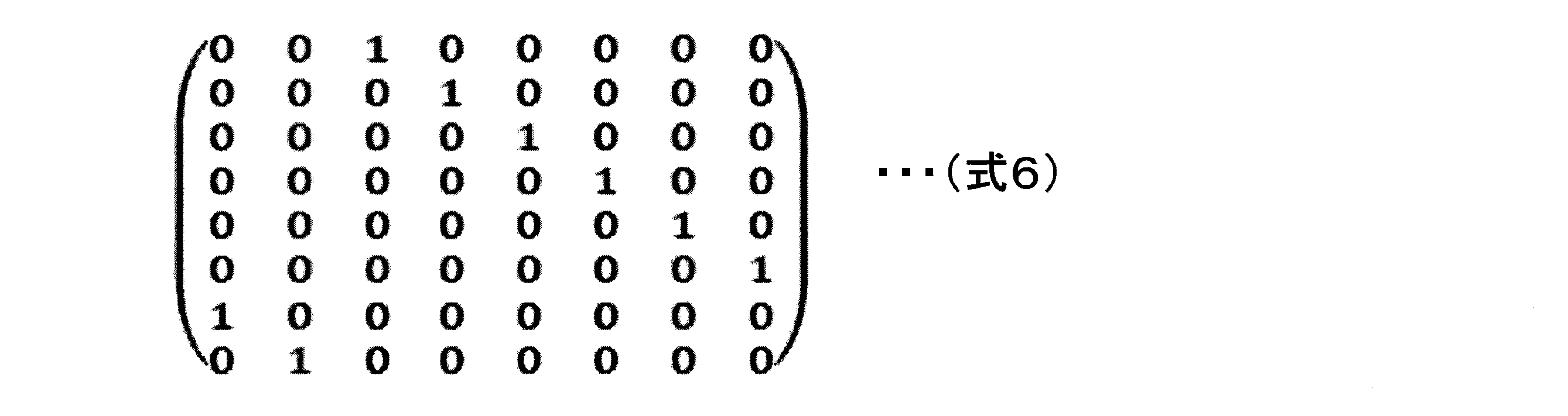
[スクランブラ246g-4]

Jビットから構成されるビット列に対してこのような行列を作用させることで、ビットの順序が異なる4種類のビット列が得られる。それぞれの行列は、単位行列および単位行列の任意の行を複数回入れ替えたものとなっている。それぞれの行列は、その転置行列が逆行列となる、すなわちA-1=Atであるという特徴を有する。したがって、スクランブラ246gにて作用させた行列の転置行列に相当する行列をデスクランブラ2333gで作用させることにより、スクランブラ246gによってスクランブル処理される前のビット列を復元することが可能である。ここで、Aはスクランブラ246gで作用させる行列を表す。例えば、符号化前のビット列を[10010111]とすると、各スクランブラ246gからの出力は以下の通りとなる。
スクランブラ246g-1からの出力:[10010111]スクランブラ246g-2からの出力:[00101111]スクランブラ246g-3からの出力:[01011110]スクランブラ246g-4からの出力:[11100101]
ビットマッピング部250で実行するビットマッピングとして、従来のグレイ符号を適用する。例えば、「00→0、01→1、11→2、10→3」という割り当てを行う。
このようなビットマッピングを適用することで、4シンボルから構成される4値シンボル列が生成される。各スクランブラ246gに対応する4値シンボル列はそれぞれ、以下の通りとなる。
このようなビットマッピングを適用することで、4シンボルから構成される4値シンボル列が生成される。各スクランブラ246gに対応する4値シンボル列はそれぞれ、以下の通りとなる。
スクランブラ246g-1に対応する4値シンボル列:3112スクランブラ246g-2に対応する4値シンボル列:0322スクランブラ246g-3に対応する4値シンボル列:1123スクランブラ246g-4に対応する4値シンボル列:2311
ビットデマッピングにおいても、グレイ符号に基づいて4値シンボルを2ビットに変換することで、4値シンボル列からビット列を復元することができる。ビットマッピングから出力された4値シンボル列に対して、スクランブラ番号を付与する。例えば、4値シンボルの最後に、スクランブラ番号に対応するシンボルを付与する。付与するシンボルの例としては、
スクランブラ246g-1に対応する付与シンボル:0
スクランブラ246g-2に対応する付与シンボル:1
スクランブラ246g-3に対応する付与シンボル:2
スクランブラ246g-4に対応する付与シンボル:3
スクランブラ246g-2に対応する付与シンボル:1
スクランブラ246g-3に対応する付与シンボル:2
スクランブラ246g-4に対応する付与シンボル:3
が挙げられる。これに加えて、ブロック間の変動を抑えるためにシンボルの両端に2を付与すると、スクランブラ番号付与部247g-1~247g-kからの出力は以下の通りとなる。
スクランブラ246g-1に対応する出力:2031122スクランブラ246g-2に対応する出力:2103222スクランブラ246g-3に対応する出力:2211232スクランブラ246g-4に対応する出力:2323112
コスト値算出部248では、これらの4値シンボル列それぞれに対してコスト値を算出する。コスト値として式2で示したコスト値を用いるとすると、各スクランブラ246gに対応する出力のコスト値は以下の通りとなり、スクランブラ246g-3からの出力が最もコスト値が小さい4値シンボル系列であることがわかる。したがって、スクランブラ246g-3に対応する出力が、最も信号変動が小さい4値シンボル列であるという結論を得る。系列選択部では、スクランブラ246g-3に対応する出力、すなわち[2211232]を送信する4値シンボル列として選択する。
スクランブラ246g-1に対応する出力のコスト値:56スクランブラ246g-2に対応する出力のコスト値:33スクランブラ246g-3に対応する出力のコスト値:7スクランブラ246g-4に対応する出力のコスト値:22
光受信器20の信号復号部233gでは、4値シンボル列に付与されているスクランブラ番号を確認する。今の例では受信した4値シンボル系列は[2211232]であるので、2番目のシンボルの値「2」から、スクランブラ番号3であると認識する。スクランブラ番号除去部2332では、スクランブラ番号付与部247gで付与した最初の2シンボルと最後の1シンボルを除去する。
これにより得られる4値シンボル列は[1123]である。ビットデマッピング部2334では、グレイ符号に基づいて4値シンボルを2値シンボルに変換する。これによって8ビット列である[01011110]を得る。このビット列に対してデスクランブラ2333g-3で、スクランブラ246g-3で作用させた行列の転置行列に相当する以下の式8の行列を作用させることにより、符号化前のビット列である[10010111]を得る。
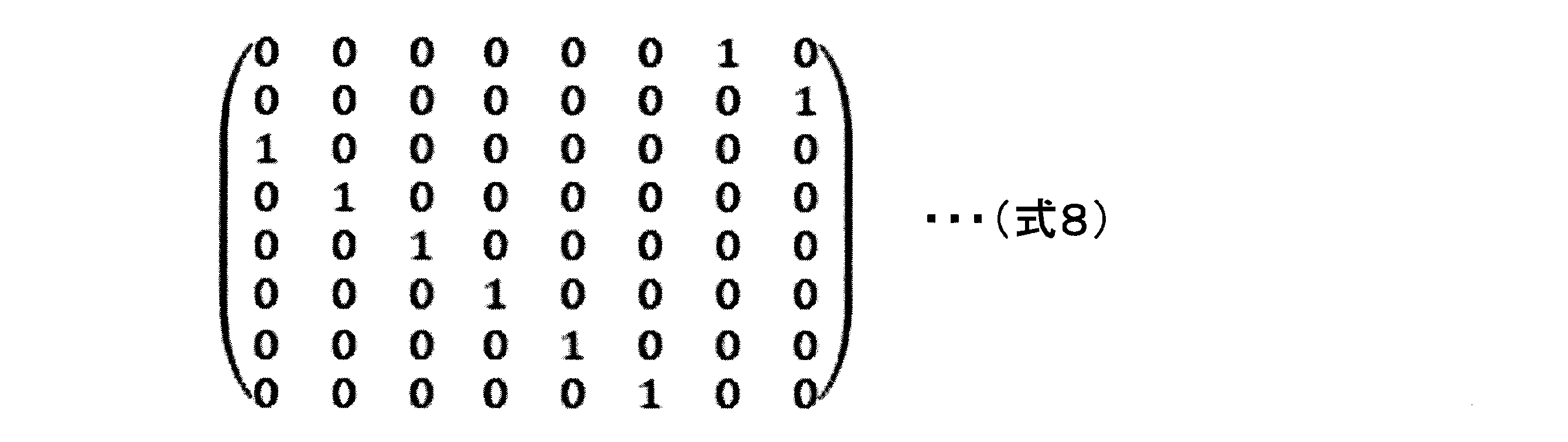
図21及び図22は、非線形符号化後の4値シンボル系列に対する信号スペクトルと、従来のPAM4信号に相当するN=128のPAM4信号の信号スペクトルを示す図である。図21(A)及び図22(A)は符号化前の4値シンボルの信号スペクトルを示す図であり、図21(B)及び図22(B)は本発明における非線形符号化によって得られた符号化後の4値シンボルの信号スペクトルを示す図である。図21及び図22において、横軸は周波数を表し、縦軸は信号パワーを表す。
なお、図21及び図20では、J=256,L=4,N=132,K=16としている。
ここではシンボル系列に対してロールオフ係数0.01のレイズドコサインフィルタを適用している。符号化率は128/132=0.97であり、符号化に伴って付与される冗長度は3%である。図21におけるコスト値の算出には式1を、図22におけるコスト値の算出には式2を用いている。
ここではシンボル系列に対してロールオフ係数0.01のレイズドコサインフィルタを適用している。符号化率は128/132=0.97であり、符号化に伴って付与される冗長度は3%である。図21におけるコスト値の算出には式1を、図22におけるコスト値の算出には式2を用いている。
図21(B)及び図22(B)に示すように、符号化後のシンボル系列では高周波成分の発生が抑圧されており、信号パワーが低周波領域に集中している。すなわち、信号スペクトルの狭帯域化が実現されている。この狭帯域化によって、光伝送システムに内在する帯域制限や波長分散による波形劣化の影響が低減される。
以上のように構成された第9の実施形態における光伝送システム100によれば、ビット系列からL値シンボル系列を生成することができる。これにより、データ情報がビット系列として入力された場合であっても上記の各実施形態における処理を行うことができる。
上述した実施形態における光送信器10,10a,10b,10c及び光受信器20,20a,20b,20cの一部または全ての機能をコンピュータで実現するようにしてもよい。その場合、この機能を実現するためのプログラムをコンピュータ読み取り可能な記録媒体に記録して、この記録媒体に記録されたプログラムをコンピュータシステムに読み込ませ、実行することによって実現してもよい。なお、ここでいう「コンピュータシステム」とは、OSや周辺機器等のハードウェアを含むものとする。また、「コンピュータ読み取り可能な記録媒体」とは、フレキシブルディスク、光磁気ディスク、ROM、CD-ROM等の可搬媒体、コンピュータシステムに内蔵されるハードディスク等の記憶装置のことをいう。さらに「コンピュータ読み取り可能な記録媒体」とは、インターネット等のネットワークや電話回線等の通信回線を介してプログラムを送信する場合の通信線のように、短時間の間、動的にプログラムを保持するもの、その場合のサーバやクライアントとなるコンピュータシステム内部の揮発性メモリのように、一定時間プログラムを保持しているものも含んでもよい。また上記プログラムは、前述した機能の一部を実現するためのものであってもよく、さらに前述した機能をコンピュータシステムにすでに記録されているプログラムとの組み合わせで実現できるものであってもよく、FPGA(Field Programmable Gate Array)等のプログラマブルロジックデバイスを用いて実現されるものであってもよい。
以上、この発明の実施形態について図面を参照して詳述してきたが、具体的な構成はこの実施形態に限られるものではなく、この発明の要旨を逸脱しない範囲の設計等も含まれる。
10、10a、10b、10c…光送信器, 11、11a-1、11a-2、11f、11g…信号符号化部, 12、12b、12a-1、12a-2、12c-1、12c-2…DA変換器, 13…信号光源, 14…光変調器, 15…光ベクトル変調器, 16、16c-1、16c-2…誤り訂正符号化部, 20、20a、20b、20c…光受信器, 21…受光部, 22、22a-1、22a-2…AD変換器, 23、23a、23b、23c、23d…デジタル信号処理部, 24…局発光源, 25…コヒーレント受信器, 231、231a…デジタルフィルタ, 232、232a、232a-1、232a-2…信号判定部, 233、233a-1、233a-2、233b、233c-1、233c-2、233d、233e-1、233e-2、233f、233g…信号復号部, 2331…復号系列選択部, 2332-1~2332-k…スクランブラ番号除去部, 2333-1~2333-k、2333g-1~2333g-k…デスクランブラ, 2334-1~2334-k…ビットデマッピング部, 234…IQ合成部, 235、235e…IQ分離部, 236、236a-1、236a-2…誤り訂正復号部, 237、237e…第1デジタルフィルタ, 238、238e-1、238e-2…ビタビ復号部, 239、239e…第2デジタルフィルタ, 240、240e-1、240e-2…加算器, 241、241e-1、241e-2…メトリック算出部, 242…位相推定部, 243…IQ合成部, 244…IQ分離部, 246-1~246-k、246g-1~246g-k…スクランブラ, 247-1~247-k、247g-1~247g-k…スクランブラ番号付与部, 248-1~248-k…コスト値算出部, 249…系列選択部, 250-1~250-k…ビットマッピング部
Claims (8)
- 光送信器と、光受信器とを備える光伝送システムであって、
前記光送信器は、
データ情報として入力されたM(Mは1以上の整数)値シンボル系列又はビット系列に対して非線形ブロック符号化を施すことにより、前記M値シンボル系列又はビット系列に1:1で対応するL(Lは2以上の整数、ただしL>M)値シンボル系列を生成する信号符号化部と、
生成された前記L値シンボル系列をアナログ信号に変換するデジタルアナログ変換部と、
前記アナログ信号に基づいて変調を行うことによって光変調信号を生成する変調器と、
を備え、
前記光受信器は、
前記光送信器から送信された光変調信号を受光し、電気信号に変換する受光部と、
前記電気信号に対して前記信号符号化部による処理と逆の処理を行うことによって前記M値シンボル系列又はビット系列を復元する信号復号部と、
を備える光伝送システム。 - 前記信号符号化部は、前記データ情報としてN(Nは1以上の整数)個のシンボルから構成されるM値シンボル系列が入力された場合、想定される一部又は全てのL値シンボル列であるL(N+P)個(Pは0以上の整数)のL値シンボル列のうち、コスト値が小さいものから順にMN個のM値シンボル列に割り当てる、請求項1に記載の光伝送システム。
- 前記信号符号化部は、L(N+P)個のL値シンボル列すべてに対して、離散フーリエ変換を行うことによってL値シンボル列それぞれの信号スペクトルを取得し、取得した信号スペクトルに基づいて以下の式1を用いて信号スペクトル広がりσ2を前記コスト値として算出する、請求項2に記載の光伝送システム。

- 前記信号符号化部は、前記データ情報としてN(Nは1以上の整数)個のシンボルから構成されるM値シンボル系列が入力された場合、想定される一部又は全てのL値シンボル列であるL(N+P)個(Pは0以上の整数)のL値シンボル列のうち、以下の式2及び式3から算出される信号スペクトル広がりσ2をコスト値として、前記コスト値が小さいものから順にMN個のM値シンボル列に割り当てる、請求項1に記載の光伝送システム。

- 前記信号符号化部は、前記データ情報として1ブロックJ(Jは1以上の整数)ビットで構成されるビット系列が入力された場合、LN(Nは1以上の整数)個のL値シンボル列の中からコスト値が小さいL値シンボル列から順に2J個を抽出し、JビットにL値シンボル列を1:1で割り当てる、請求項1に記載の光伝送システム。
- 前記光送信器は、非線形ブロック符号化の後に誤り訂正符号化を行う誤り訂正符号化部をさらに備え、
前記光受信器は、非線形ブロック復号の前に誤り訂正復号を行う誤り訂正復号部をさらに備える、請求項1から5のいずれか一項に記載の光伝送システム。 - 前記光受信器は、L値シンボル系列に対する信号復調において最尤系列推定に基づく判定を行う、請求項1から6のいずれか一項に記載の光伝送システム。
- 前記信号符号化部は、前記M値シンボル列をN+P-1個のL値シンボルから構成されるL値シンボル列に変換することによって、異なるK種類のL値シンボル列を生成する複数のスクランブラ部と、
前記K種類のL値シンボル列それぞれに対して、スクランブラ番号を示すシンボルを付与する複数のスクランブラ番号付与部と、
前記L値シンボル列それぞれに対してコスト値を算出する複数のコスト値算出部と、
前記K種類のL値シンボル列の中からコスト値が最小の系列を選択する系列選択部とで構成され、
前記信号復号部は、前記L値シンボル列からスクランブラ番号を示すシンボルを除去する複数のスクランブラ番号除去部と、
前記スクランブラ番号に応じたデスクランブラを使用して、前記スクランブラ部による符号化処理の逆変換に相当する復号化処理を実行し、符号化前のシンボル系列であるM値シンボル列を復元する複数のデスクランブラで構成される、請求項1から7のいずれか一項に光伝送システム。
Priority Applications (1)
| Application Number | Priority Date | Filing Date | Title |
|---|---|---|---|
| US17/291,170 US11581944B2 (en) | 2018-11-08 | 2019-11-07 | Optical transmission system |
Applications Claiming Priority (2)
| Application Number | Priority Date | Filing Date | Title |
|---|---|---|---|
| JP2018-210832 | 2018-11-08 | ||
| JP2018210832A JP7193715B2 (ja) | 2018-11-08 | 2018-11-08 | 光伝送システム |
Publications (1)
| Publication Number | Publication Date |
|---|---|
| WO2020095986A1 true WO2020095986A1 (ja) | 2020-05-14 |
Family
ID=70612049
Family Applications (1)
| Application Number | Title | Priority Date | Filing Date |
|---|---|---|---|
| PCT/JP2019/043650 Ceased WO2020095986A1 (ja) | 2018-11-08 | 2019-11-07 | 光伝送システム |
Country Status (3)
| Country | Link |
|---|---|
| US (1) | US11581944B2 (ja) |
| JP (1) | JP7193715B2 (ja) |
| WO (1) | WO2020095986A1 (ja) |
Cited By (1)
| Publication number | Priority date | Publication date | Assignee | Title |
|---|---|---|---|---|
| WO2022044077A1 (ja) * | 2020-08-24 | 2022-03-03 | 日本電信電話株式会社 | シンボル判定装置及びタップ選択方法 |
Families Citing this family (1)
| Publication number | Priority date | Publication date | Assignee | Title |
|---|---|---|---|---|
| CN117424648A (zh) * | 2023-10-23 | 2024-01-19 | 上海交通大学 | 基于非均匀保护编码调制的数字前传方法及系统 |
Citations (6)
| Publication number | Priority date | Publication date | Assignee | Title |
|---|---|---|---|---|
| US20020044073A1 (en) * | 2000-08-11 | 2002-04-18 | Gottfried Ungerboeck | System and method for Huffman shaping in a data communication system |
| JP2006517374A (ja) * | 2003-02-07 | 2006-07-20 | コデオス コミュニケーションズ,インコーポレイテッド | フィルタ−付き三レベル式送信機 |
| JP2016521465A (ja) * | 2013-06-19 | 2016-07-21 | 三菱電機株式会社 | 光通信のためにデータを変調する方法およびシステム |
| JP2018509860A (ja) * | 2015-04-01 | 2018-04-05 | 華為技術有限公司Huawei Technologies Co.,Ltd. | ルックアップテーブル生成方法およびルックアップテーブル生成装置、ならびに事前補償方法および事前補償装置 |
| WO2018074412A1 (ja) * | 2016-10-18 | 2018-04-26 | 日本電信電話株式会社 | 符号化装置及び復号化装置 |
| WO2018167920A1 (ja) * | 2017-03-16 | 2018-09-20 | 三菱電機株式会社 | 信号整形装置、整形終端装置、信号整形方法および光伝送方法 |
Family Cites Families (1)
| Publication number | Priority date | Publication date | Assignee | Title |
|---|---|---|---|---|
| US9112653B2 (en) | 2013-06-19 | 2015-08-18 | Mitsubishi Electric Research Laboratories, Inc. | Method and system for modulating optical signals as high-dimensional lattice constellation points to increase tolerance to noise |
-
2018
- 2018-11-08 JP JP2018210832A patent/JP7193715B2/ja active Active
-
2019
- 2019-11-07 WO PCT/JP2019/043650 patent/WO2020095986A1/ja not_active Ceased
- 2019-11-07 US US17/291,170 patent/US11581944B2/en active Active
Patent Citations (6)
| Publication number | Priority date | Publication date | Assignee | Title |
|---|---|---|---|---|
| US20020044073A1 (en) * | 2000-08-11 | 2002-04-18 | Gottfried Ungerboeck | System and method for Huffman shaping in a data communication system |
| JP2006517374A (ja) * | 2003-02-07 | 2006-07-20 | コデオス コミュニケーションズ,インコーポレイテッド | フィルタ−付き三レベル式送信機 |
| JP2016521465A (ja) * | 2013-06-19 | 2016-07-21 | 三菱電機株式会社 | 光通信のためにデータを変調する方法およびシステム |
| JP2018509860A (ja) * | 2015-04-01 | 2018-04-05 | 華為技術有限公司Huawei Technologies Co.,Ltd. | ルックアップテーブル生成方法およびルックアップテーブル生成装置、ならびに事前補償方法および事前補償装置 |
| WO2018074412A1 (ja) * | 2016-10-18 | 2018-04-26 | 日本電信電話株式会社 | 符号化装置及び復号化装置 |
| WO2018167920A1 (ja) * | 2017-03-16 | 2018-09-20 | 三菱電機株式会社 | 信号整形装置、整形終端装置、信号整形方法および光伝送方法 |
Non-Patent Citations (1)
| Title |
|---|
| BOCHERER,GEORG ET AL.: "Bandwidth Efficient and Rate-Matched Low-Density Parity-Check Coded Modulation", IEEE TRANSACTIONS ON COMMUNICATIONS, vol. 63, no. 12, December 2015 (2015-12-01), pages 4651 - 4665, XP011593618, DOI: 10.1109/TCOMM.2015.2494016 * |
Cited By (3)
| Publication number | Priority date | Publication date | Assignee | Title |
|---|---|---|---|---|
| WO2022044077A1 (ja) * | 2020-08-24 | 2022-03-03 | 日本電信電話株式会社 | シンボル判定装置及びタップ選択方法 |
| JP7495637B2 (ja) | 2020-08-24 | 2024-06-05 | 日本電信電話株式会社 | シンボル判定装置及びタップ選択方法 |
| US12231173B2 (en) | 2020-08-24 | 2025-02-18 | Nippon Telegraph And Telephone Corporation | Symbol determination device and tap selection method |
Also Published As
| Publication number | Publication date |
|---|---|
| JP2020078001A (ja) | 2020-05-21 |
| US11581944B2 (en) | 2023-02-14 |
| US20210367670A1 (en) | 2021-11-25 |
| JP7193715B2 (ja) | 2022-12-21 |
Similar Documents
| Publication | Publication Date | Title |
|---|---|---|
| JP6681217B2 (ja) | 光情報伝送システム、及び光送信器 | |
| CN110169027B (zh) | 转换或再转换数据信号方法、数据发送和接收方法和系统 | |
| JP6499301B2 (ja) | 複数の変調を用いた離散マルチトーン伝送のための方法及びシステム | |
| JP4927617B2 (ja) | データ伝送装置および伝送符号の生成方法 | |
| US11444694B2 (en) | Optical transmission system | |
| JP7193715B2 (ja) | 光伝送システム | |
| CN112054977B (zh) | 一种基于功率谱整形的光传输方法及装置 | |
| CN109314530A (zh) | 光接收机、光传输装置和光接收机用的方法 | |
| US10693562B2 (en) | Encoding device and decoding device | |
| WO2017216836A1 (ja) | 光伝送方法及び光伝送システム | |
| CN105610516A (zh) | 基于超奈奎斯特系统的光调制方法及其相应的解调方法 | |
| JP4884959B2 (ja) | 光ディジタル伝送システムおよび方法 | |
| JP6470198B2 (ja) | 光送受信システム | |
| WO2020121901A1 (ja) | 光伝送システム、光送信機、光受信機及び伝達関数推定方法 | |
| JP7328581B2 (ja) | 光伝送システム、光送信機及び光受信機 | |
| CN114928409B (zh) | 信号处理的方法、装置及系统 | |
| CN112787723B (zh) | 一种非线性编码器、编码方法及光传输系统 | |
| CN116961825A (zh) | 编码方法、解码方法和光通信系统 | |
| Kodama et al. | Stream-binary-data padded digital multicarrier DP-M-QAM for secure bi-directional optical transmission | |
| CN109565436B (zh) | Pam-4传输系统中的时钟和数据恢复 | |
| Ying et al. | Sparse volterra model based on single side-band optical NPAM-4 direct-detection system | |
| JP2016144198A (ja) | 光送信機、光受信機、光伝送装置、光伝送システム、光送信方法、光受信方法及び光伝送方法 | |
| CN120785480A (zh) | 一种基于概率幅度整形的快速正交频分复用调制方法及系统 | |
| JP2019092100A (ja) | 光受信装置 |
Legal Events
| Date | Code | Title | Description |
|---|---|---|---|
| 121 | Ep: the epo has been informed by wipo that ep was designated in this application |
Ref document number: 19882463 Country of ref document: EP Kind code of ref document: A1 |
|
| NENP | Non-entry into the national phase |
Ref country code: DE |
|
| 122 | Ep: pct application non-entry in european phase |
Ref document number: 19882463 Country of ref document: EP Kind code of ref document: A1 |