WO2020095850A1 - 固体撮像装置、固体撮像装置の製造方法および電子機器 - Google Patents
固体撮像装置、固体撮像装置の製造方法および電子機器 Download PDFInfo
- Publication number
- WO2020095850A1 WO2020095850A1 PCT/JP2019/043110 JP2019043110W WO2020095850A1 WO 2020095850 A1 WO2020095850 A1 WO 2020095850A1 JP 2019043110 W JP2019043110 W JP 2019043110W WO 2020095850 A1 WO2020095850 A1 WO 2020095850A1
- Authority
- WO
- WIPO (PCT)
- Prior art keywords
- layer
- imaging device
- state imaging
- solid
- light shielding
- Prior art date
- Legal status (The legal status is an assumption and is not a legal conclusion. Google has not performed a legal analysis and makes no representation as to the accuracy of the status listed.)
- Ceased
Links
Images















Classifications
-
- H—ELECTRICITY
- H10—SEMICONDUCTOR DEVICES; ELECTRIC SOLID-STATE DEVICES NOT OTHERWISE PROVIDED FOR
- H10F—INORGANIC SEMICONDUCTOR DEVICES SENSITIVE TO INFRARED RADIATION, LIGHT, ELECTROMAGNETIC RADIATION OF SHORTER WAVELENGTH OR CORPUSCULAR RADIATION
- H10F39/00—Integrated devices, or assemblies of multiple devices, comprising at least one element covered by group H10F30/00, e.g. radiation detectors comprising photodiode arrays
- H10F39/80—Constructional details of image sensors
- H10F39/807—Pixel isolation structures
-
- H—ELECTRICITY
- H04—ELECTRIC COMMUNICATION TECHNIQUE
- H04N—PICTORIAL COMMUNICATION, e.g. TELEVISION
- H04N25/00—Circuitry of solid-state image sensors [SSIS]; Control thereof
- H04N25/70—SSIS architectures; Circuits associated therewith
-
- H—ELECTRICITY
- H04—ELECTRIC COMMUNICATION TECHNIQUE
- H04N—PICTORIAL COMMUNICATION, e.g. TELEVISION
- H04N25/00—Circuitry of solid-state image sensors [SSIS]; Control thereof
- H04N25/70—SSIS architectures; Circuits associated therewith
- H04N25/76—Addressed sensors, e.g. MOS or CMOS sensors
- H04N25/77—Pixel circuitry, e.g. memories, A/D converters, pixel amplifiers, shared circuits or shared components
-
- H—ELECTRICITY
- H10—SEMICONDUCTOR DEVICES; ELECTRIC SOLID-STATE DEVICES NOT OTHERWISE PROVIDED FOR
- H10F—INORGANIC SEMICONDUCTOR DEVICES SENSITIVE TO INFRARED RADIATION, LIGHT, ELECTROMAGNETIC RADIATION OF SHORTER WAVELENGTH OR CORPUSCULAR RADIATION
- H10F39/00—Integrated devices, or assemblies of multiple devices, comprising at least one element covered by group H10F30/00, e.g. radiation detectors comprising photodiode arrays
- H10F39/011—Manufacture or treatment of image sensors covered by group H10F39/12
- H10F39/014—Manufacture or treatment of image sensors covered by group H10F39/12 of CMOS image sensors
-
- H—ELECTRICITY
- H10—SEMICONDUCTOR DEVICES; ELECTRIC SOLID-STATE DEVICES NOT OTHERWISE PROVIDED FOR
- H10F—INORGANIC SEMICONDUCTOR DEVICES SENSITIVE TO INFRARED RADIATION, LIGHT, ELECTROMAGNETIC RADIATION OF SHORTER WAVELENGTH OR CORPUSCULAR RADIATION
- H10F39/00—Integrated devices, or assemblies of multiple devices, comprising at least one element covered by group H10F30/00, e.g. radiation detectors comprising photodiode arrays
- H10F39/011—Manufacture or treatment of image sensors covered by group H10F39/12
- H10F39/024—Manufacture or treatment of image sensors covered by group H10F39/12 of coatings or optical elements
-
- H—ELECTRICITY
- H10—SEMICONDUCTOR DEVICES; ELECTRIC SOLID-STATE DEVICES NOT OTHERWISE PROVIDED FOR
- H10F—INORGANIC SEMICONDUCTOR DEVICES SENSITIVE TO INFRARED RADIATION, LIGHT, ELECTROMAGNETIC RADIATION OF SHORTER WAVELENGTH OR CORPUSCULAR RADIATION
- H10F39/00—Integrated devices, or assemblies of multiple devices, comprising at least one element covered by group H10F30/00, e.g. radiation detectors comprising photodiode arrays
- H10F39/10—Integrated devices
- H10F39/12—Image sensors
- H10F39/18—Complementary metal-oxide-semiconductor [CMOS] image sensors; Photodiode array image sensors
-
- H—ELECTRICITY
- H10—SEMICONDUCTOR DEVICES; ELECTRIC SOLID-STATE DEVICES NOT OTHERWISE PROVIDED FOR
- H10F—INORGANIC SEMICONDUCTOR DEVICES SENSITIVE TO INFRARED RADIATION, LIGHT, ELECTROMAGNETIC RADIATION OF SHORTER WAVELENGTH OR CORPUSCULAR RADIATION
- H10F39/00—Integrated devices, or assemblies of multiple devices, comprising at least one element covered by group H10F30/00, e.g. radiation detectors comprising photodiode arrays
- H10F39/10—Integrated devices
- H10F39/12—Image sensors
- H10F39/199—Back-illuminated image sensors
-
- H—ELECTRICITY
- H10—SEMICONDUCTOR DEVICES; ELECTRIC SOLID-STATE DEVICES NOT OTHERWISE PROVIDED FOR
- H10F—INORGANIC SEMICONDUCTOR DEVICES SENSITIVE TO INFRARED RADIATION, LIGHT, ELECTROMAGNETIC RADIATION OF SHORTER WAVELENGTH OR CORPUSCULAR RADIATION
- H10F39/00—Integrated devices, or assemblies of multiple devices, comprising at least one element covered by group H10F30/00, e.g. radiation detectors comprising photodiode arrays
- H10F39/80—Constructional details of image sensors
- H10F39/802—Geometry or disposition of elements in pixels, e.g. address-lines or gate electrodes
-
- H—ELECTRICITY
- H10—SEMICONDUCTOR DEVICES; ELECTRIC SOLID-STATE DEVICES NOT OTHERWISE PROVIDED FOR
- H10F—INORGANIC SEMICONDUCTOR DEVICES SENSITIVE TO INFRARED RADIATION, LIGHT, ELECTROMAGNETIC RADIATION OF SHORTER WAVELENGTH OR CORPUSCULAR RADIATION
- H10F39/00—Integrated devices, or assemblies of multiple devices, comprising at least one element covered by group H10F30/00, e.g. radiation detectors comprising photodiode arrays
- H10F39/80—Constructional details of image sensors
- H10F39/805—Coatings
- H10F39/8057—Optical shielding
-
- H—ELECTRICITY
- H10—SEMICONDUCTOR DEVICES; ELECTRIC SOLID-STATE DEVICES NOT OTHERWISE PROVIDED FOR
- H10F—INORGANIC SEMICONDUCTOR DEVICES SENSITIVE TO INFRARED RADIATION, LIGHT, ELECTROMAGNETIC RADIATION OF SHORTER WAVELENGTH OR CORPUSCULAR RADIATION
- H10F39/00—Integrated devices, or assemblies of multiple devices, comprising at least one element covered by group H10F30/00, e.g. radiation detectors comprising photodiode arrays
- H10F39/80—Constructional details of image sensors
- H10F39/811—Interconnections
-
- H—ELECTRICITY
- H10—SEMICONDUCTOR DEVICES; ELECTRIC SOLID-STATE DEVICES NOT OTHERWISE PROVIDED FOR
- H10F—INORGANIC SEMICONDUCTOR DEVICES SENSITIVE TO INFRARED RADIATION, LIGHT, ELECTROMAGNETIC RADIATION OF SHORTER WAVELENGTH OR CORPUSCULAR RADIATION
- H10F39/00—Integrated devices, or assemblies of multiple devices, comprising at least one element covered by group H10F30/00, e.g. radiation detectors comprising photodiode arrays
- H10F39/10—Integrated devices
- H10F39/12—Image sensors
- H10F39/18—Complementary metal-oxide-semiconductor [CMOS] image sensors; Photodiode array image sensors
- H10F39/186—Complementary metal-oxide-semiconductor [CMOS] image sensors; Photodiode array image sensors having arrangements for blooming suppression
-
- H—ELECTRICITY
- H10—SEMICONDUCTOR DEVICES; ELECTRIC SOLID-STATE DEVICES NOT OTHERWISE PROVIDED FOR
- H10F—INORGANIC SEMICONDUCTOR DEVICES SENSITIVE TO INFRARED RADIATION, LIGHT, ELECTROMAGNETIC RADIATION OF SHORTER WAVELENGTH OR CORPUSCULAR RADIATION
- H10F39/00—Integrated devices, or assemblies of multiple devices, comprising at least one element covered by group H10F30/00, e.g. radiation detectors comprising photodiode arrays
- H10F39/80—Constructional details of image sensors
- H10F39/803—Pixels having integrated switching, control, storage or amplification elements
- H10F39/8037—Pixels having integrated switching, control, storage or amplification elements the integrated elements comprising a transistor
Definitions
- the present disclosure relates to a solid-state imaging device, a method for manufacturing a solid-state imaging device, and electronic equipment.
- CMOS Complementary Metal Oxide Semiconductor
- the present disclosure proposes a solid-state imaging device, a method for manufacturing the solid-state imaging device, and an electronic apparatus that can reduce light leakage from adjacent unit pixels.
- a solid-state imaging device includes a semiconductor layer, a light blocking wall, and an insulating layer.
- the semiconductor layer is provided with a plurality of photoelectric conversion units and a plurality of charge holding units that hold the charges generated by the photoelectric conversion units.
- the light shielding wall is provided inside the groove formed in the semiconductor layer in the depth direction from the light incident side between the photoelectric conversion unit and the charge holding unit which are adjacent to each other.
- the insulating layer is provided on the side opposite to the light incident side of the semiconductor layer, and has an opening that surrounds the groove.
- a solid-state imaging device includes a semiconductor layer, a light blocking wall, and an insulating layer.
- a plurality of photoelectric conversion units are provided in the semiconductor layer.
- the light shielding wall is provided inside the groove formed in the semiconductor layer in the depth direction from the light incident side between the adjacent photoelectric conversion units.
- the insulating layer is provided on the side opposite to the light incident side of the semiconductor layer, and has an opening that surrounds the groove.
- a method for manufacturing a solid-state imaging device includes a step of forming an insulating layer on a semiconductor substrate, a step of forming an opening in a predetermined region of the insulating layer, and a step of forming another insulating layer so as to fill the opening. And a step of grinding the surface of the semiconductor substrate opposite to the side on which the insulating layer is formed. Further, the method for manufacturing a solid-state imaging device includes a step of forming a groove portion in a depth direction from a ground surface of the semiconductor substrate toward the opening portion, and a step of forming a light shielding wall inside the groove portion. Including.
- FIG. 1 is a system configuration diagram illustrating a schematic configuration example of a solid-state imaging device according to a first embodiment of the present disclosure.
- FIG. 3 is a circuit diagram showing a configuration example of a unit pixel of the solid-state imaging device according to the first embodiment of the present disclosure.
- FIG. 3 is a cross-sectional view schematically showing the light blocking structure of the solid-state imaging device according to the first embodiment of the present disclosure. It is an expanded sectional view which shows typically one manufacturing process of the solid-state imaging device in a reference example. It is an expanded sectional view which shows typically one manufacturing process of the solid-state imaging device in a reference example. It is an expanded sectional view which shows typically one manufacturing process of the solid-state imaging device in a reference example. It is an expanded sectional view which shows typically one manufacturing process of the solid-state imaging device in a reference example.
- FIG. 1 is a system configuration diagram illustrating a schematic configuration example of a solid-state imaging device according to a first embodiment of the present disclosure.
- FIG. 4 is an enlarged cross-sectional view schematically showing one manufacturing process of the solid-state imaging device according to the first embodiment of the present disclosure.
- FIG. 4 is an enlarged cross-sectional view schematically showing one manufacturing process of the solid-state imaging device according to the first embodiment of the present disclosure.
- FIG. 4 is an enlarged cross-sectional view schematically showing one manufacturing process of the solid-state imaging device according to the first embodiment of the present disclosure. It is a figure which shows typically the planar structure of the solid-state imaging device which concerns on the 1st Embodiment of this indication. It is a figure which shows typically the planar structure of the solid-state imaging device which concerns on the 1st Embodiment of this indication.
- FIG. 4 is an enlarged cross-sectional view schematically showing one manufacturing process of the solid-state imaging device according to the first embodiment of the present disclosure.
- FIG. 4 is an enlarged cross-sectional view schematically showing one manufacturing process of the solid-state imaging device according to the first embodiment of the present disclosure.
- FIG. 4 is an enlarged cross-sectional view schematically showing one manufacturing process of the solid-state imaging device according to the first embodiment of the present disclosure.
- FIG. 4 is an enlarged cross-sectional view schematically showing one manufacturing process of the solid-state imaging device according to the first embodiment of the present disclosure.
- FIG. 3 is a flowchart showing a procedure of manufacturing steps of the solid-state imaging device according to the first embodiment of the present disclosure.
- FIG. 8 is an enlarged cross-sectional view schematically showing a light shielding structure of a solid-state imaging device according to Modification 1 of the first embodiment of the present disclosure.
- FIG. 9 is an enlarged cross-sectional view schematically showing a light-shielding structure of a solid-state imaging device according to Modification 2 of the first embodiment of the present disclosure.
- FIG. 9 is an enlarged cross-sectional view schematically showing a light-shielding structure of a solid-state imaging device according to Modification 3 of the first embodiment of the present disclosure.
- FIG. 8 is an enlarged cross-sectional view schematically showing a light shielding structure of a solid-state imaging device according to Modification 1 of the first embodiment of the present disclosure.
- FIG. 9 is an enlarged cross-sectional view schematically showing a light-shielding structure of a solid-state imaging device according
- FIG. 10 is an enlarged cross-sectional view schematically showing a light shielding structure of a solid-state imaging device according to Modification 4 of the first embodiment of the present disclosure.
- FIG. 11 is an enlarged cross-sectional view schematically showing a light-shielding structure of a solid-state imaging device according to Modification 5 of the first embodiment of the present disclosure.
- FIG. 11 is an enlarged cross-sectional view schematically showing one manufacturing process of the solid-state imaging device according to Modification 4 of the first embodiment of the present disclosure.
- FIG. 11 is an enlarged cross-sectional view schematically showing one manufacturing process of the solid-state imaging device according to Modification 4 of the first embodiment of the present disclosure.
- FIG. 11 is an enlarged cross-sectional view schematically showing one manufacturing process of the solid-state imaging device according to Modification 4 of the first embodiment of the present disclosure.
- FIG. 11 is an enlarged cross-sectional view schematically showing one manufacturing process of the solid-state imaging device according to Modification 4 of the first embodiment of the present disclosure.
- FIG. 11 is an enlarged cross-sectional view schematically showing one manufacturing process of the solid-state imaging device according to Modification 4 of the first embodiment of the present disclosure.
- FIG. 11 is an enlarged cross-sectional view schematically showing one manufacturing process of the solid-state imaging device according to Modification 4 of the first embodiment of the present disclosure.
- FIG. 11 is an enlarged cross-sectional view schematically showing one manufacturing process of the solid-state imaging device according to Modification 4 of the first embodiment of the present disclosure.
- FIG. 11 is an enlarged cross-sectional view schematically showing one manufacturing process of the solid-state imaging device according to Modification 4 of the first embodiment of the present disclosure.
- FIG. 11 is an enlarged cross-sectional view schematically showing one manufacturing process of the solid-state imaging device according to Modification 4 of the first embodiment of the present disclosure. It is sectional drawing which shows typically the light-shielding structure of the solid-state imaging device which concerns on the 2nd Embodiment of this indication. It is an expanded sectional view which shows typically the light-shielding structure of the solid-state imaging device concerning the 2nd Embodiment of this indication.
- FIG. 13 is an enlarged cross-sectional view schematically showing a light-shielding structure of a solid-state imaging device according to Modification 6 of the second embodiment of the present disclosure.
- FIG. 16 is an enlarged cross-sectional view schematically showing a light-shielding structure of a solid-state imaging device according to Modification 7 of the second embodiment of the present disclosure.
- FIG. 16 is a block diagram illustrating a configuration example of an electronic device according to each embodiment of the present disclosure.
- FIG. 1 is a system configuration diagram illustrating a schematic configuration example of a solid-state imaging device 1 according to the first embodiment of the present disclosure.
- a solid-state imaging device 1 that is a CMOS image sensor includes a pixel array unit 10, a system control unit 12, a vertical drive unit 13, a column read circuit unit 14, a column signal processing unit 15, and The horizontal drive unit 16 and the signal processing unit 17 are provided.
- the pixel array unit 10, the system control unit 12, the vertical drive unit 13, the column read circuit unit 14, the column signal processing unit 15, the horizontal drive unit 16, and the signal processing unit 17 are electrically connected to each other on the same semiconductor substrate. It is provided on a plurality of laminated semiconductor substrates.
- the pixel array section 10 is an effective unit pixel having a photoelectric conversion element (photodiode 21 (see FIG. 2)) capable of photoelectrically converting the amount of charge according to the amount of incident light, accumulating it internally, and outputting it as a signal.
- photoelectric conversion element photodiode 21 (see FIG. 2)
- unit pixel are two-dimensionally arranged in a matrix.
- the pixel array unit 10 includes a dummy unit pixel having a structure without the photodiode 21, a light-shielding unit pixel in which light from the outside is blocked by shielding the light-receiving surface, and the like. , And may include regions arranged in rows and / or columns.
- the light-shielding unit pixel may have the same configuration as the effective unit pixel 11 except that the light-receiving surface has a light-shielding structure. Further, hereinafter, the photocharge having the charge amount corresponding to the incident light amount may be simply referred to as “charge”, and the unit pixel 11 may be simply referred to as “pixel”.
- a pixel drive line LD is formed for each row along the left-right direction (arrangement direction of pixels in a pixel row) in a matrix-shaped pixel array, and vertical pixel wiring is provided for each column.
- the LVs are formed along the vertical direction (arrangement direction of pixels in the pixel column) in the drawing.
- One end of the pixel drive line LD is connected to the output end corresponding to each row of the vertical drive unit 13.
- the column read circuit unit 14 includes at least a circuit that supplies a constant current to each unit pixel 11 in a selected row in the pixel array unit 10 for each column, a current mirror circuit, and a changeover switch for the unit pixel 11 to be read.
- the column readout circuit unit 14 constitutes an amplifier together with the transistor in the selected pixel in the pixel array unit 10, converts the photocharge signal into a voltage signal and outputs it to the vertical pixel wiring LV.
- the vertical drive unit 13 includes a shift register, an address decoder, and the like, and drives each unit pixel 11 of the pixel array unit 10 at the same time for all pixels or in units of rows. Although not specifically shown in the drawings, the vertical drive unit 13 has a read scanning system and a sweep scanning system or a batch sweep and batch transfer system.
- the read scanning system sequentially selects and scans the unit pixels 11 of the pixel array unit 10 row by row in order to read pixel signals from the unit pixels 11.
- row driving rolling shutter operation
- a sweeping scan is performed prior to the read scan by a shutter speed for a read row in which the read scan system performs the read scan.
- the electronic shutter operation means an operation of discarding unnecessary photocharges accumulated in the photodiode 21 until immediately before and starting a new exposure (starting accumulation of photocharges).
- the signal read by the read operation by the read scanning system corresponds to the amount of light incident after the read operation immediately before that or the electronic shutter operation.
- the period from the read timing of the immediately previous read operation or the sweep timing of the electronic shutter operation to the read timing of the current read operation is the photocharge accumulation time (exposure time) in the unit pixel 11.
- the time from batch sweep to batch transfer is the accumulation time (exposure time).
- the pixel signal output from each unit pixel 11 in the pixel row selectively scanned by the vertical drive unit 13 is supplied to the column signal processing unit 15 through each vertical pixel wiring LV.
- the column signal processing unit 15 performs, for each pixel column of the pixel array unit 10, predetermined signal processing on a pixel signal output from each unit pixel 11 of a selected row through the vertical pixel wiring LV, and after the signal processing, The pixel signal is temporarily held.
- the column signal processing unit 15 performs at least noise removal processing, for example, CDS (Correlated Double Sampling) processing as signal processing.
- CDS Correlated Double Sampling
- the column signal processing unit 15 By the CDS processing by the column signal processing unit 15, fixed noise peculiar to pixels such as reset noise and threshold variation of the amplification transistor AMP is removed.
- the column signal processing unit 15 may be configured to have, for example, an AD conversion function in addition to the noise removal processing so as to output a pixel signal as a digital signal.
- the horizontal drive unit 16 includes a shift register, an address decoder, etc., and sequentially selects unit circuits corresponding to the pixel columns of the column signal processing unit 15. By the selective scanning by the horizontal driving unit 16, the pixel signals processed by the column signal processing unit 15 are sequentially output to the signal processing unit 17.
- the system control unit 12 includes a timing generator that generates various timing signals, and based on the various timing signals generated by the timing generator, the vertical drive unit 13, the column signal processing unit 15, the horizontal drive unit 16, and the like. Drive control is performed.
- the solid-state imaging device 1 further includes a signal processing unit 17 and a data storage unit (not shown).
- the signal processing unit 17 has at least an addition processing function and performs various signal processing such as addition processing on the pixel signals output from the column signal processing unit 15.
- the data storage unit temporarily stores the data required for the signal processing in the signal processing unit 17 during the signal processing.
- the signal processing unit 17 and the data storage unit may be an external signal processing unit provided on a board different from the solid-state imaging device 1, for example, a DSP (Digital Signal Processor) or software processing. It may be mounted on the same substrate as 1.
- DSP Digital Signal Processor
- FIG. 2 is a circuit diagram showing a configuration example of the unit pixel 11 of the solid-state imaging device 1 according to the first embodiment of the present disclosure.
- the unit pixel 11 includes a photodiode (PD) 21.
- the photodiode 21 is an example of a photoelectric conversion unit.
- the photodiode 21 is formed, for example, by forming the p-type layer 21a on the substrate surface side of the p-type well layer 23 formed on the n-type substrate 22 and burying the n-type buried layer 21b.
- the photodiode 21 is an embedded photodiode.
- the n-type buried layer 21b has an impurity concentration that causes a depletion state when discharging charges.
- the unit pixel 11 includes a TRY gate 24, a TX1 gate 25a, a TX2 gate 25b, and a charge holding unit (MEM) 26 in addition to the photodiode 21.
- the TRY gate 24 is connected between the photodiode 21 and the charge holding unit 26.
- the TX1 gate 25a and the TX2 gate 25b are arranged near the charge holding unit 26.
- the charge holding portion 26 is formed, for example, by forming the p-type layer 26a on the substrate surface side of the p-type well layer 23 formed on the n-type substrate 22 and burying the n-type buried layer 26b.
- the n-type buried layer 26b of the charge holding unit 26 may be formed by an n-type diffusion region.
- the n-type diffusion region may be formed inside the p-type well layer 23, and the p-type layer 26a may be formed on the substrate surface side.
- the dark current generated at the Si-SiO 2 interface can be suppressed from being accumulated in the n-type diffusion region of the charge holding unit 26, and thus the image quality of the solid-state imaging device 1 can be improved.
- the TRY gate 24 photoelectrically converts by the photodiode 21 when the drive signal TRY is applied to the gate electrode, and transfers the charge accumulated inside the photodiode 21 to the charge holding unit 26. Further, the TRY gate 24 also functions as a gate for preventing charges from flowing back from the charge holding unit 26 to the photodiode 21.
- the TX1 gate 25a functions as a gate when transferring charges from the charge holding unit 26 to a floating diffusion region (FD: Floating Diffusion) 28 described later.
- the TX1 gate 25a also functions as a gate for holding the charge in the charge holding unit 26.
- the TX2 gate 25b functions as a gate when transferring charges from the photodiode 21 to the charge holding unit 26.
- the TX2 gate 25b also functions as a gate for holding the charges in the charge holding unit 26.
- the charge holding unit 26 is modulated by applying the drive signal TX2 and the drive signal TX1 to the gate electrode of the TX2 gate 25b and the gate electrode of the TX1 gate 25a, respectively.
- the drive signal TX2 and the drive signal TX1 are applied to the gate electrode of the TX2 gate 25b and the gate electrode of the TX1 gate 25a, respectively, whereby the potential of the charge holding portion 26 can be deepened.
- the saturated charge amount of the charge holding unit 26 can be increased as compared with the case where no modulation is applied.
- the unit pixel 11 further includes a TRG gate 27 and a floating diffusion region 28.
- the TRG gate 27 transfers the charge accumulated in the charge holding unit 26 to the floating diffusion region 28 by applying the drive signal TRG to the gate electrode.
- the floating diffusion region 28 is a charge-voltage conversion unit including an n-type layer, and converts the charge transferred from the charge holding unit 26 by the TRG gate 27 into a voltage.
- the unit pixel 11 further includes a reset transistor (RST) 29, an amplification transistor (AMP) 30, and a selection transistor (SEL) 31.
- RST reset transistor
- AMP amplification transistor
- SEL selection transistor
- FIG. 2 shows an example in which n-channel MOS transistors are used for the reset transistor 29, the amplification transistor 30, and the selection transistor 31.
- the configurations of the reset transistor 29, the amplification transistor 30, and the selection transistor 31 are not limited to the example shown in FIG.
- the reset transistor 29 is connected between the power supply Vrst and the floating diffusion region 28.
- the reset transistor 29 resets the floating diffusion region 28 by applying the drive signal RST to the gate electrode.
- the amplification transistor 30 has a drain electrode connected to the power supply Vdd and a gate electrode connected to the floating diffusion region 28, and reads the voltage of the floating diffusion region 28.
- the drain electrode of the selection transistor 31 is connected to the source electrode of the amplification transistor 30, and the source electrode is connected to the vertical signal line (VSL) 32.
- the selection transistor 31 selects the unit pixel 11 from which the pixel signal is to be read by applying the drive signal SEL to the gate electrode.
- the selection transistor 31 is connected between the source electrode of the amplification transistor 30 and the vertical signal line 32, but the selection transistor 31 is connected to the power supply Vdd and the drain electrode of the amplification transistor 30. You may connect in between.
- one or more of the reset transistor 29, the amplification transistor 30, and the selection transistor 31 may be omitted depending on the pixel signal reading method.
- the unit pixel 11 is provided with an overflow gate (OFG) 33 for preventing blooming.
- the overflow gate 33 discharges the charges of the photodiode 21 to the n-type layer 34 connected to the power supply Vdd by applying the drive signal OFG to the gate electrode at the start of exposure.
- the solid-state imaging device 1 having the unit pixel 11 described so far can realize global shutter operation (global exposure) by starting exposure of all pixels simultaneously and ending exposure of all pixels simultaneously. By this global shutter operation, it is possible to realize image pickup without distortion due to the exposure period in which all the pixels match.
- the unit pixel 11 is formed by forming the n-type buried channel in the p-type p-type well layer 23, but the conductivity types may be opposite to each other. In this case, the potential relationships described below are all reversed.
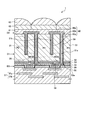
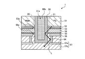
- FIG. 3 is a cross-sectional view schematically showing the light shielding structure of the solid-state imaging device 1 according to the first embodiment of the present disclosure.
- the layer 56 and the wiring layer 57 are laminated.
- the LP-SiN layer 53 is an example of an insulating layer
- the P-SiN layer 54 is an example of another insulating layer.
- a gate electrode 58 is provided at a predetermined position inside the insulating multilayer film including the SiO layer 52, the LP-SiN layer 53, the P-SiN layer 54, and the SiO layer 55.
- the back surface irradiation is performed in which the photodiode 21 is irradiated with light from the back surface side opposite to the front surface of the semiconductor layer 51 on which the wiring layer 57 is laminated.
- Type image pickup device
- a flattening film 61, a color filter 62, and a microlens 63 are laminated on the back surface side of the semiconductor layer 51 which is irradiated with light from the outside.
- a support substrate is laminated below the wiring layer 57.
- the back surface of the semiconductor layer 51 is also referred to as an incident surface
- the front surface of the semiconductor layer 51 which is arranged at the boundary with the wiring layer 57, is also referred to as a boundary surface.
- the surface of the photodiode 21 on the incident surface side of the semiconductor layer 51 is referred to as a light receiving surface
- the surface opposite to the light receiving surface is referred to as a bottom surface.
- the surface of the charge holding portion 26 on the incident surface side of the semiconductor layer 51 is also referred to as an upper surface
- the surface opposite to the upper surface is also referred to as a bottom surface.
- the semiconductor layer 51 includes, for example, silicon.
- the semiconductor layer 51 has a plurality of photodiodes 21 and a plurality of charge holding units 26. It should be noted that one unit pixel 11 (see FIG. 1) is provided with a pair of photodiodes 21 and charge holding portions 26.
- the SiO layer 52 is composed of, for example, a silicon oxide film.
- the SiO layer 52 has a function of a gate insulating film between the semiconductor layer 51 and the gate electrode 58.
- the gate electrode 58 corresponds to, for example, the gate electrode of the TRY gate 24 shown in FIG.
- the LP (Low Pressure) -SiN layer 53 is composed of, for example, a silicon nitride film formed by a low pressure CVD (Chemical Vapor Deposition) method.
- the LP-SiN layer 53 has a higher film density than the surrounding SiO layer 52, P-SiN layer 54 and SiO layer 55.
- the P (Plasma) -SiN layer 54 is composed of, for example, a silicon nitride film formed by a plasma CVD method.
- the SiO layer 55 is composed of, for example, a silicon oxide film.
- the insulating multilayer film including the SiO layer 52, the LP-SiN layer 53, the P-SiN layer 54, and the SiO layer 55 described above is used as the TRY gate in the solid-state imaging device 1 according to the first embodiment. Used in forming device structures such as 24.
- the SiO layer 52 may be set to a thickness of 10 nm or more, for example. This is, for example, a thickness necessary for processing adjustment of the depth of the groove penetrating the semiconductor layer 51 for forming the light shielding wall 60b (described later). On the other hand, since the SiO layer 52 also serves as an insulating film between the gate electrode 58 and the semiconductor layer 51, it is not desirable to make it too thick. Therefore, the thickness of the SiO layer 52 may be set in the range of 10 nm to 20 nm, for example.
- the laminated film composed of the LP-SiN layer 53 and the P-SiN layer 54 is preferably set to have a thickness of 50 nm or more, for example. This is a thickness necessary for, for example, processing adjustment of the contact formed in the wiring layer 57 and processing control of a groove portion 51a (described later) that penetrates the semiconductor layer 51 for forming the light shielding wall 60b.
- the thickness is, for example, a thickness necessary for preventing a groove for forming a contact from reaching the semiconductor layer 51 and preventing the semiconductor layer 51 from being damaged due to damage caused by processing the contact. Further, such a thickness is a thickness necessary for stopping the groove portion 51a penetrating the semiconductor layer 51 for forming the light shielding wall 60b with the laminated film.
- the thickness of the laminated film formed of the LP-SiN layer 53 and the P-SiN layer 54 may be set in the range of 50 nm to 100 nm, for example.
- the SiO layer 55 may be set to have a thickness of 25 nm or more, for example. This is, for example, a thickness required to prevent the SiO layer 55 from being damaged and the laminated film of the LP-SiN layer 53 and the P-SiN layer 54 from being exposed when the light shielding layer 56 is processed.
- the thickness of the SiO layer 55 may be set in the range of 30 nm to 100 nm, for example.
- the light shielding layer 56 is made of, for example, a metal film having a light shielding property.
- the material of the light shielding layer 56 may be any material that shields light, and for example, tungsten (W), aluminum (Al), copper (Cu), or the like can be used.
- the light shielding layer 56 prevents the light, which is not absorbed by the photodiode 21 and transmitted through the semiconductor layer 51, from entering the wiring layer 57. Accordingly, it is possible to prevent the light transmitted through the semiconductor layer 51 from entering the wiring layer 57, being reflected by the wiring film 57a of the wiring layer 57, and leaking to the adjacent charge holding portions 26 and the like.
- FIG. 3 shows an example in which the light shielding layer 56 is arranged so as to cover the bottom surface side of the photodiode 21 and the charge holding portion 26, the arrangement of the light shielding layer 56 is not limited to such an example.
- the light shielding layer 56 may be arranged so as to cover only the bottom surface side of the charge holding unit 26.
- the wiring layer 57 has a plurality of wiring films 57a and an interlayer insulating film 57b.
- the wiring film 57a is made of aluminum, copper or the like
- the interlayer insulating film 57b is made of a silicon oxide film or the like.
- an opening (not shown) is formed in the light shielding layer 56, and a through via (not shown) that penetrates the opening is formed.
- a through via (not shown) that penetrates the opening is formed.
- a groove 51 a and a groove 51 b are formed between the photodiode 21 and the charge holding portion 26 which are adjacent to each other in the semiconductor layer 51.
- the groove 51a is formed so as to penetrate the semiconductor layer 51 from the incident surface of the semiconductor layer 51 in the depth direction.
- the groove portion 51b is formed so as not to penetrate the semiconductor layer 51 and extend from the incident surface of the semiconductor layer 51 to the middle of the semiconductor layer 51 in the depth direction.
- a multilayer film 59 and a light shielding portion 60 are provided on the groove portions 51a and 51b and the incident surface of the semiconductor layer 51.
- the multilayer film 59 is formed on the incident surface of the semiconductor layer 51 and the inner walls of the grooves 51a and 51b.
- the multilayer film 59 includes, for example, a fixed charge film, an antireflection film, and an insulating film.
- the light shielding portion 60 formed on the surface of the multilayer film 59 is made of, for example, a metal film having a light shielding property.
- the material of the light shielding portion 60 may be any material that shields light, and for example, tungsten, aluminum, copper or the like can be used.
- the light shielding unit 60 suppresses the light incident from the incident surface of the semiconductor layer 51 from directly or indirectly leaking into the charge holding unit 26.
- the light shielding portion 60 has a front light shielding portion 60a, a light shielding wall 60b, and a non-penetrating light shielding wall 60c.
- the front light-shielding portion 60a covers a region of the incident surface of the semiconductor layer 51 except above the light-receiving surface of the photodiode 21. That is, the surface light-shielding portion 60a covers a region of the light-receiving surface of the semiconductor layer 51 except a region where light is incident on the photodiode 21.
- the light shielding wall 60b penetrates the semiconductor layer 51 from the incident surface of the semiconductor layer 51 and reaches the bottom surface of the semiconductor layer 51.
- the non-penetrating light-shielding wall 60c does not penetrate the semiconductor layer 51 and extends from the incident surface of the semiconductor layer 51 to the middle of the semiconductor layer 51.
- the light shielding wall 60b is provided, for example, in a different unit pixel 11 and is arranged between the photodiode 21 and the charge holding unit 26 which are adjacent to each other.
- the non-penetrating light shielding wall 60c is arranged, for example, between the photodiode 21 and the charge holding unit 26 in the same unit pixel 11.
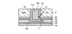
- an opening 53a is provided in the LP-SiN layer 53 so as to surround the groove 51a penetrating the semiconductor layer 51.
- the opening 53a is provided in the region where the groove 51a is formed in the LP-SiN layer 53.
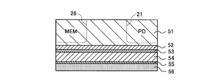
- FIGS. 4A to 5C are enlarged cross-sectional views schematically showing one manufacturing process of the solid-state imaging device 1 in the reference example, which is an enlarged view of a region where the groove portion 51a and the light shielding layer 56 are close to each other.
- the reference examples shown in FIGS. 4A to 4C show the case where the opening 53a is not provided in the LP-SiN layer 53.
- the photodiode 21 and the charge holding portion 26 are attached to the semiconductor substrate 151 (see FIG. 9A) used to form the semiconductor layer 51. It is formed.
- the SiO layer 52, the LP-SiN layer 53, the P-SiN layer 54, the SiO layer 55, the light shielding layer 56, and the wiring layer 57 are laminated. Then, a support substrate (not shown) is attached. Then, the semiconductor layer 51 is formed by grinding the back surface of the semiconductor substrate 151, and the state shown in FIG. 4A is obtained.
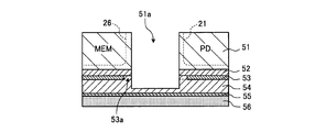
- the groove portion 51a is formed between the photodiode 21 and the charge holding portion 26. ..
- the groove 51a is formed, for example, by forming a hard mask (not shown) having a desired opening on the back surface of the semiconductor layer 51 and selectively etching the semiconductor layer 51 in the depth direction through the hard mask. It is formed.
- the insulating multilayer film including the SiO layer 52, the LP-SiN layer 53, the P-SiN layer 54 and the SiO layer 55 is used as a stopper.
- the film density of the LP-SiN layer 53 is higher than that of the SiO layer 52, the P-SiN layer 54 and the SiO layer 55, the LP-SiN layer 53 may not be sufficiently etched. Therefore, in the reference example, as shown in FIG. 4B, the LP-SiN layer 53 remains so as to project into the groove 51a.
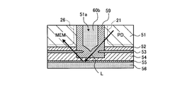
- the tip of the light shielding wall 60b does not have a rectangular shape but has a tapered wedge shape as shown in FIG. 4C. turn into.
- the multilayer film 59 is formed by a method having high coverage such as ALD (Atomic Layer Deposition) method, it is formed not only on the inner wall of the groove 51a but also on the surface of the protruding LP-SiN layer 53. Because it will be done.
- ALD Atomic Layer Deposition
- the light L reaching the region where the groove 51 a and the light shielding layer 56 are close to each other from the inside of the photodiode 21 may not be shielded by the light shielding wall 60 b.
- the unshielded light L is reflected by the light shielding layer 56, so that the light L leaks into the adjacent charge holding portions 26.
- the tip of the light shielding wall 60b has a tapered wedge shape, so that the adjacent unit pixels 11 It becomes difficult to reduce the leakage of light from the.
- 5A to 5C are enlarged cross-sectional views schematically showing one manufacturing process of the solid-state imaging device 1 according to the first embodiment of the present disclosure.
- the photodiode 21 and the charge holding portion 26 are formed on the semiconductor substrate 151 (see FIG. 9A) used to form the semiconductor layer 51. It
- the SiO layer 52, the LP-SiN layer 53, the P-SiN layer 54, the SiO layer 55, the light shielding layer 56, and the wiring layer 57 are laminated. Then, a support substrate (not shown) is attached. As will be described in detail later, during the laminating step, the LP-SiN layer 53 is provided with an opening 53a, and the opening 53a is filled with the P-SiN layer 54.
- the semiconductor layer 51 is formed by grinding the back surface of the semiconductor substrate 151, and the state shown in FIG. 5A is obtained.
- a groove portion 51 a is formed between the photodiode 21 and the charge holding portion 26 in order to form the light shielding wall 60 b between the adjacent photodiode 21 and the charge holding portion 26. ..
- the groove 51a is formed, for example, by forming a hard mask (not shown) having a desired opening on the back surface of the semiconductor layer 51 and selectively etching the semiconductor layer 51 in the depth direction through the hard mask. It is formed.
- the insulating multilayer film including the SiO layer 52, the LP-SiN layer 53, the P-SiN layer 54 and the SiO layer 55 is used as a stopper.
- the opening 53a is provided in advance in the region where the groove 51a is formed.
- the LP-SiN layer 53 is not originally provided in the region where the groove 51a is formed, the LP-SiN layer 53 is not etched and remains in the groove 51a. Can be suppressed.
- a multilayer film 59 is formed on the inner wall of the groove 51a by using the ALD method or the like, and then the inside of the groove 51a is filled with a metal film to form a light shielding wall 60b.
- the tip shape of the light shielding wall 60b has a rectangular shape similar to the shape of the groove portion 51a.
- the light L that reaches the region where the groove 51a and the light shielding layer 56 are close to each other from the inside of the photodiode 21 can be blocked by the light shielding wall 60b. Therefore, according to the first embodiment, it is possible to reduce the leakage of light from the adjacent unit pixels 11.
- the size of the opening 53a is preferably larger than the portion of the groove 51a surrounded by the opening 53a when viewed from the light incident side. As a result, it is possible to further suppress the LP-SiN layer 53 from remaining so as to project into the groove 51a when forming the groove 51a.
- the LP-SiN layer 53 which is an example of an insulating layer, may be composed of a silicon nitride film formed by a low pressure CVD method. Thereby, a highly reliable transistor can be formed in the solid-state imaging device 1.
- the LP-SiN layer 53 is composed of the silicon nitride film formed by the low pressure CVD method, but the material of the LP-SiN layer 53 is not limited to this example. ..
- the LP-SiN layer 53 is formed by the low pressure CVD method as long as it has a higher film density than the surrounding SiO layer 52, P-SiN layer 54 and SiO layer 55. Also, a material different from the silicon nitride film may be used.
- the insulating multilayer film used when forming a device structure such as the TRY gate 24 and used as a stopper when forming the groove 51a has a four-layer structure.
- the insulating multilayer film is not limited to the four-layer structure of the SiO layer 52, the LP-SiN layer 53, the P-SiN layer 54, and the SiO layer 55, and may be a multilayer structure including the LP-SiN layer 53.
- FIGS. 6 to 8. are diagrams schematically showing the planar structure of the solid-state imaging device 1 according to the first embodiment of the present disclosure.
- FIG. 6 shows a cross section near the depth D1 shown in FIG. 3
- FIG. 7 shows a cross section near the depth D2 shown in FIG. 3
- FIG. 8 shows a cross section near the depth D3 shown in FIG. Indicates.
- different hatching is added to each of the light-shielding walls 60b and the non-penetrating light-shielding walls 60c so that they can be easily identified.
- description will be made using the vertical and horizontal directions in FIGS. 6 to 8.
- one unit pixel 11 is shown as the center, and a part of the unit pixels 11 around it is also shown.
- the arrangement of each unit in the vertically adjacent unit pixel 11 is similar to the arrangement of the unit pixel 11 shown in the center, and the arrangement of each unit in the unit pixels 11 adjacent to the left and right is the unit shown in the center.
- the pixels 11 are symmetrical with respect to the arrangement of the pixels 11.
- a TRY gate 24, a TX2 gate 25b, a TX1 gate 25a, and a TRG gate 27 are arranged on the photodiode 21 from left to right.
- the contact 70a and the contact 70b are arranged side by side in the approximate center of the TRY gate 24, and the contact 70c and the contact 70d are arranged side by side in the approximate center of the TX2 gate 25b. Further, a contact 70e and a contact 70f are arranged side by side in the left-right direction at substantially the center of the TX1 gate 25a. The contacts 70a to 70f are arranged side by side in a row.
- a contact 70g and a contact 70h are arranged vertically. Then, the charge holding unit 26 is arranged so as to substantially overlap the TRY gate 24, the TX2 gate 25b, and the TX1 gate 25a.
- a gate portion 29a of the reset transistor 29 (see FIG. 2)
- a gate portion 30a of the amplification transistor 30 (see FIG. 2)
- a gate portion 31a of the selection transistor 31 (see FIG. 2). It is arranged so that it is lined up and down.
- a contact 70i is arranged on the gate portion 29a, and a contact 70j is arranged on the lower end of the gate portion 29a.
- a contact 70k is arranged between the gate portion 29a and the gate portion 30a.
- a contact 70l and a contact 70m are arranged in the vertical direction at substantially the center of the gate portion 30a.
- the contacts 70i to 70m are arranged side by side in a line up and down.
- a contact 70n and a contact 70o are arranged side by side between the gate portion 30a and the gate portion 31a, and a contact 70p and a contact 70q are arranged side by side at the substantially center of the gate portion 31a. To be done. Under the gate portion 31a, the contacts 70r and the contacts 70s are arranged side by side in the left-right direction.
- the contact 70n, the contact 70p, and the contact 70r are arranged vertically in a line. Further, the contact 70o, the contact 70q, and the contact 70s are arranged vertically in a line.
- An overflow gate 33 is arranged to the left of the photodiode 21. Above the inside of the overflow gate 33, the contacts 70t and the contacts 70u are arranged vertically. The contact 70v is arranged in the recessed portion at the lower end of the overflow gate 33, and the contact 70w is arranged under the overflow gate 33. The contacts 70t to 70w are arranged vertically in a line.
- the periphery (side surface) of the photodiode 21 is surrounded by the light shielding wall 60b and the non-penetrating light shielding wall 60c of the light shielding unit 60.
- the light-shielding wall 60b and the non-penetrating light-shielding wall 60c are connected without interruption in a direction parallel to the incident surface of the semiconductor layer 51, and surround the periphery (side surface) of the photodiode 21 without interruption.
- the non-penetrating light-shielding wall 60c is also connected without interruption to the unit pixels 11 that are adjacent to the left and right.
- the light shielding wall 60b of the light shielding portion 60 surrounding the photodiode 21 is arranged between the photodiode 21 and the TX1 gate 25a and the TX2 gate 25b in the same unit pixel 11 as the photodiode 21.
- the light blocking wall 60b is arranged between the photodiode 21 and the charge holding portions 26 of the unit pixels 11 that are vertically adjacent to each other.
- a non-penetrating light-shielding wall 60c is arranged in a portion other than the above in the light-shielding portion 60 surrounding the periphery of the photodiode 21. Specifically, the non-penetrating light shielding wall 60c is arranged between the photodiode 21 and the unit pixels 11 that are adjacent to each other on the left and right. This is for forming the gate portion and contact of each transistor.
- a non-penetrating light shielding wall 60c is arranged between the photodiode 21 and the TRY gate 24 in the same unit pixel 11. This is to ensure a path for the charge to flow from the photodiode 21 to the charge holding unit 26.
- the non-penetrating light shielding wall 60c is arranged at a connecting portion (a portion where the non-penetrating light shielding wall 60c intersects) between the non-penetrating light shielding wall 60c extending in the left-right direction and the non-penetrating light shielding wall 60c extending in the vertical direction. This is because if the light shielding wall 60b is formed in this portion, etching may be accelerated by the microloading phenomenon and the light shielding wall 60b may reach the wiring layer 57.
- the side surface of the photodiode 21 is surrounded by the non-penetrating light shielding wall 60c and the light shielding wall 60b. Accordingly, it is possible to prevent the light incident on the incident surface of the semiconductor layer 51 from passing through the photodiode 21 and leaking to the adjacent photodiode 21, the charge holding portion 26, or the like.
- the first embodiment it is possible to suppress the generation of optical noise due to light leaking into the adjacent photodiode 21 or charge holding unit 26.
- the light-shielding wall 60b is penetrated from the semiconductor layer 51 to enlarge the light-shielding region, so that the incidence of light on the charge holding portion 26 can be further suppressed.
- the pinning is strengthened by applying the negative bias to the light shielding wall 60b, so that the generation of the dark current can be suppressed.
- the p-type well layer 23 of the semiconductor layer 51 can be made to have a low concentration, so that the surface charge density Qs of the semiconductor layer 51 and the capacity of the charge holding portion 26 can be increased. Therefore, according to the first embodiment, the pixel characteristics can be improved.
- the shaded portion in FIG. 7 indicates the area where the front light-shielding portion 60a is arranged. As shown in FIG. 7, the front light-shielding portion 60 a covers the area of the incident surface of the semiconductor layer 51 except the light-receiving surface of the photodiode 21.
- the area of the incident surface of the semiconductor layer 51 except the area where the light is incident on the photodiode 21 is covered with the surface light shielding portion 60a.
- the first embodiment it is possible to prevent the light that has entered the incident surface of the semiconductor layer 51 from entering the region of the photodiode 21 other than the light receiving surface.
- the shaded portion in FIG. 8 indicates the region where the light shielding layer 56 is arranged. As shown in FIG. 8, the light shielding layer 56 is arranged in a region excluding the active region in the boundary surface of the semiconductor layer 51 and the region in which the contacts 70a to 70w are arranged.
- the bottom surface of the photodiode 21 is entirely covered with the light shielding layer 56. Further, the bottom surface of the charge holding portion 26 is substantially covered with the light shielding layer 56, except for the active area on the boundary surface of the semiconductor layer 51 and the area where the contacts 70a to 70f are arranged.
- the light shielding layer 56 on the bottom surface of the semiconductor layer 51, the light incident on the incident surface of the semiconductor layer 51 passes through the inside of the photodiode 21 and is reflected by the wiring film 57a, and the adjacent photodiode 21 and Leakage into the charge holding portion 26 and the like can be suppressed.
- the first embodiment it is possible to suppress the generation of optical noise due to light leaking into the adjacent photodiode 21 or charge holding unit 26.
- FIGS. 9A to 10 are enlarged cross-sectional views schematically showing one manufacturing process of the solid-state imaging device 1 according to the first embodiment of the present disclosure.
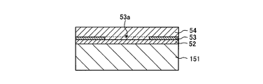
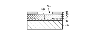
- a SiO layer 52 having a predetermined thickness is formed on the surface of the semiconductor substrate 151 used for forming the semiconductor layer 51 (see FIG. 3) by a known method. Subsequently, an LP-SiN layer 53 having a predetermined thickness is formed on the SiO layer 52 by a low pressure CVD method or the like.
- an opening 53a is formed in a region where a groove 51a will be formed later.
- the opening 53a forms, for example, a hard mask (not shown) having a desired opening on the surface of the LP-SiN layer 53, and the LP-SiN layer 53 is selectively formed in the depth direction through the hard mask. It is formed by dry etching.
- a P-SiN layer 54 having a predetermined thickness is formed on the LP-SiN layer 53 by a plasma CVD method or the like so as to fill the opening 53a.
- a SiO layer 55 having a predetermined thickness is formed on the P-SiN layer 54 by a known method, and a light shielding layer 56 having a predetermined thickness is formed on the SiO layer 55.
- the film is formed by the method.
- the wiring layer 57 (see FIG. 3) is formed on the light shielding layer 56 by a known method, and the support substrate is bonded onto the wiring layer 57. Then, the back surface of the semiconductor substrate 151 is ground by a known method to form the semiconductor layer 51 having a predetermined thickness. As a result, the state shown in FIG. 5A is obtained.
- a groove 51a is formed between the photodiode 21 and the charge holding portion 26.
- the groove 51a is formed, for example, by forming a hard mask (not shown) having a desired opening on the back surface of the semiconductor layer 51 and selectively etching the semiconductor layer 51 in the depth direction through the hard mask. It is formed.
- the etching process for forming the groove 51a is performed by using the insulating multilayer film including the SiO layer 52, the LP-SiN layer 53, the P-SiN layer 54 and the SiO layer 55 as a stopper. Good to do.
- the etching process for forming the groove 51a reaches the light-shielding layer 56 made of a metal film, metal such as tungsten is released from the exposed light-shielding layer 56 to the outside, and the device under formation is formed. May be contaminated with such metal. The contamination may deteriorate the dark characteristics of the device.
- the first embodiment by using the above-mentioned insulating multilayer film as the stopper, it is possible to prevent the etching process for forming the groove 51a from reaching the light shielding layer 56. Therefore, according to the first embodiment, metal contamination caused by the light shielding layer 56 can be suppressed, so that the dark characteristics of the device can be favorably maintained.
- a multilayer film 59 is formed on the inner wall of the groove 51a by using the ALD method or the like, and the inside of the groove 51a is filled with a metal film by a known method to form a light shielding wall 60b.
- the metal film covering the light receiving surface of the photodiode 21 is etched to form an opening, and the flattening film 61, the color filter 62, the microlens 63, etc. are formed.
- the unit pixel 11 of the solid-state imaging device 1 according to the embodiment is completed.
- FIG. 10 is a flowchart showing the procedure of the manufacturing process of the solid-state imaging device 1 according to the first embodiment of the present disclosure.
- the SiO layer 52 is formed on the surface of the semiconductor substrate 151 (step S101).
- the LP-SiN layer 53 is formed on the SiO layer 52 (step S102).
- the opening 53a is formed in a predetermined region of the LP-SiN layer 53 (step S103). Then, the P-SiN layer 54 is formed on the LP-SiN layer 53 so as to fill the opening 53a (step S104).
- the SiO layer 55 is formed on the P-SiN layer 54 (step S105), and the light shielding layer 56 is formed on the SiO layer 55 (step S106).
- the wiring layer 57 is formed on the light shielding layer 56 (step S107), and the support substrate is attached to the wiring layer 57 (step S108).
- step S109 the back surface of the semiconductor substrate 151 is ground (step S109) to form the semiconductor layer 51.
- the groove 51a is formed in the depth direction from the ground surface toward the opening 53a (step S110).
- the multilayer film 59 is formed on the inner wall of the groove 51a (step S111). Then, the light shielding wall 60b is formed in the groove 51a by filling the inside of the groove 51a with a metal film (step S112), and the process is completed.
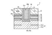
- FIG. 11 is an enlarged cross-sectional view schematically showing the light shielding structure of the solid-state imaging device 1 according to Modification 1 of the first embodiment of the present disclosure, and is a drawing corresponding to FIG. 5C of the first embodiment. ..
- an opening 56a is provided in the light shielding layer 56 so as to surround the groove 51a penetrating the semiconductor layer 51.
- the opening 56a is provided in the region of the light shielding layer 56 where the groove 51a is formed.
- the light shielding wall 60b is provided so as to reach the opening 56a.
- a light shielding wall 60b is provided so as to penetrate the opening 56a.
- the light shielding wall 60b so as to penetrate the opening 56a, as shown in FIG. 11, the light L reaching the region where the groove 51a and the light shielding layer 56 are close to each other from inside the photodiode 21 is provided. It can be blocked by the light blocking wall 60b. As a result, the leakage of light from the adjacent unit pixels 11 can be reduced.
- the opening 56a is provided in advance in the region where the groove 51a is formed, so that the light shielding layer 56 is prevented from being exposed to the outside during the etching process for forming the groove 51a. You can Therefore, according to the first modification, it is possible to suppress metal contamination due to the light shielding layer 56, and thus it is possible to favorably maintain the dark characteristics of the device.
- the size of the opening 56a when viewed from the light incident side, may be larger than the portion of the groove 51a surrounded by the opening 56a. Thereby, it is possible to further suppress the light shielding layer 56 from being exposed to the outside during the etching process for forming the groove 51a.
- the metal contamination caused by the light shielding layer 56 can be further suppressed, so that the dark characteristics of the device can be more favorably maintained.
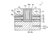
- FIG. 12 is an enlarged cross-sectional view schematically showing the light shielding structure of the solid-state imaging device 1 according to the modified example 2 of the first embodiment of the present disclosure.
- the light shielding wall 60b may be provided so that the tip portion of the light shielding wall 60b is located inside the opening 56a. That is, the tip of the light shielding wall 60b may be disposed between the upper surface (the surface on the SiO layer 55 side) 56b of the light shielding layer 56 and the lower surface (the surface on the wiring layer 57 side) 56c of the light shielding layer 56. ..
- the light shielding wall 60b is provided so that the tip end portion is arranged inside the opening portion 56a, so that the light reaching the region where the groove portion 51a and the light shielding layer 56 are close to each other from the inside of the photodiode 21 is shielded by the light shielding wall. It can be blocked by 60b.
- FIG. 13 is an enlarged cross-sectional view schematically showing the light-shielding structure of the solid-state imaging device 1 according to Modification 3 of the first embodiment of the present disclosure.
- the light shielding wall 60b may be provided so that the tip of the light shielding wall 60b reaches the opening 56a. That is, the tip of the light shielding wall 60b may be arranged so as to be substantially flush with the upper surface 56b of the light shielding layer 56.
- the light shielding wall 60b By thus providing the light shielding wall 60b so that the tip portion reaches the opening 56a, the light shielding wall 60b shields the light reaching the region where the groove 51a and the light shielding layer 56 are close to each other from the inside of the photodiode 21. You can
- FIG. 14 is an enlarged cross-sectional view schematically showing the light shielding structure of the solid-state imaging device 1 according to the modified example 4 of the first embodiment of the present disclosure.
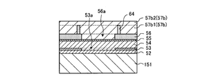
- a wall portion 64 may be provided in the wiring layer 57 adjacent to the opening portion 56a and arranged so as to block between the light shielding layer 56 and the wiring film 57a of the wiring layer 57.
- the wall portion 64 is composed of a metal film having a light shielding property.
- the material of the wall 64 may be any material that blocks light, and for example, tungsten (W), aluminum (Al), copper (Cu), or the like can be used.
- FIG. 15 is an enlarged cross-sectional view schematically showing the light-shielding structure of the solid-state imaging device 1 according to Modification 5 of the first embodiment of the present disclosure.
- the wall portion 64 may be arranged so as not to contact the light shielding layer 56 but contact only the wiring film 57a. This also makes it possible to prevent the light L reflected by the tip of the light shielding wall 60b from entering between the light shielding layer 56 and the wiring film 57a.
- FIGS. 16A to 16G are enlarged cross-sectional views schematically showing one manufacturing process of the solid-state imaging device 1 according to Modification 4 of the first embodiment of the present disclosure.
- the manufacturing process of the modified example 4 will be described below, but the manufacturing process described below can be appropriately applied to the manufacturing process of other modified examples. Further, the steps of forming the SiO layer 52, the LP-SiN layer 53 having the opening 53a, the P-SiN layer 54, the SiO layer 55, and the light shielding layer 56 on the semiconductor substrate 151 are shown in FIG. Since it is shown in FIG. 9D, details of this step are omitted.
- an opening 56a is formed in a region where a groove 51a will be formed later.
- the opening 56a is formed by, for example, forming a hard mask (not shown) having a desired opening on the surface of the light shielding layer 56 and selectively etching the light shielding layer 56 in the depth direction through the hard mask. Is formed by.
- an interlayer insulating film 57b1 having a predetermined thickness is formed on the light shielding layer 56 by a known method so as to fill the opening 56a.
- the interlayer insulating film 57b1 is an interlayer insulating film provided between the light shielding layer 56 and the wiring film 57a1 (see FIG. 16G) closest to the light shielding layer 56 in the interlayer insulating film 57b.
- the opening 57ba is formed in the region where the wall 64 is formed.
- the opening 57ba is formed, for example, by forming a hard mask (not shown) having a desired opening on the surface of the interlayer insulating film 57b1 and selectively etching the interlayer insulating film 57b1 in the depth direction through the hard mask. It is formed by
- the wall 57 is formed by filling the opening 57ba with a metal film by a known method and planarizing the surface by CMP (Chemical Mechanical Polishing) or the like. ..
- an interlayer insulating film 57b2 having a predetermined thickness is formed on the interlayer insulating film 57b1 by a known method.
- the interlayer insulating film 57b2 is an interlayer insulating film provided in the same layer of the interlayer insulating film 57b as the wiring film 57a1 closest to the light shielding layer 56.
- an opening 57bb is formed in the region where the wiring film 57a is formed in the interlayer insulating film 57b2.
- the opening 57bb forms, for example, a hard mask (not shown) having a desired opening on the surface of the interlayer insulating film 57b2, and the interlayer insulating film 57b2 is selectively etched in the depth direction through the hard mask. It is formed by
- a wiring film 57a1 is formed by embedding the opening 57bb with a metal film by a known method and flattening the surface by CMP or the like. Then, the wiring layer 57 is formed by forming the other wiring film 57a and the interlayer insulating film 57b by the same method.
- the wall portion 64 is formed so as to be in contact with at least the wiring film 57a (for example, the wiring film 57a1), so that the wall portion 64 is formed in parallel with the normal wiring layer 57 forming process. be able to.
- the support substrate is bonded onto the wiring layer 57. Then, the back surface of the semiconductor substrate 151 is ground to form the semiconductor layer 51 having a predetermined thickness.
- a groove 51a is formed between the photodiode 21 and the charge holding portion 26.
- the groove 51a is formed, for example, by forming a hard mask (not shown) having a desired opening on the back surface of the semiconductor layer 51 and selectively etching the semiconductor layer 51 in the depth direction through the hard mask. It is formed.
- the multilayer film 59 is formed on the inner wall of the groove 51a by using the ALD method or the like, and the inside of the groove 51a is filled with the metal film to form the light shielding wall 60b, thereby forming the light shielding structure of the modified example 4 shown in FIG. Can be realized.
- the opening 53a be provided in advance in the region where the groove 51a is formed in the LP-SiN layer 53. Accordingly, when the groove 51a is formed so as to reach the light shielding layer 56, it is possible to prevent the groove 51a from being deformed from a desired shape due to the LP-SiN layer 53 remaining in the groove 51a.
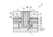
- FIG. 17 is a sectional view schematically showing the light shielding structure of the solid-state imaging device 1A according to the second embodiment of the present disclosure.
- the solid-state imaging device 1A according to the second embodiment is a backside illumination CMOS image sensor in which the charge holding unit 26 is not provided. Therefore, the semiconductor layer 51 of the solid-state imaging device 1A includes a plurality of photodiodes 21, and one unit pixel 11 (see FIG. 1) of the solid-state imaging device 1A is provided with one photodiode 21.
- a groove 51a is formed between the adjacent photodiodes 21.
- the groove 51a is formed so as to penetrate the semiconductor layer 51 from the incident surface of the semiconductor layer 51, as in the first embodiment.
- a multilayer film 59 and a light shielding portion 60 are provided on the incident surface of the semiconductor layer 51 and the groove portion 51a.
- the multilayer film 59 is formed on the incident surface of the semiconductor layer 51 and the inner wall of the groove 51a.
- the light shielding unit 60 suppresses the light incident from the incident surface of the semiconductor layer 51 from directly or indirectly leaking into the adjacent photodiode 21.
- the light shield 60 has a front light shield 60a and a light shield wall 60b.
- the front light-shielding portion 60a covers a region of the incident surface of the semiconductor layer 51 except above the light-receiving surface of the photodiode 21. That is, the surface light-shielding portion 60a covers a region of the light-receiving surface of the semiconductor layer 51 except a region where light is incident on the photodiode 21.
- the light shielding wall 60b extends from the incident surface of the semiconductor layer 51 through the semiconductor layer 51 to the bottom surface of the semiconductor layer 51.
- the light shielding wall 60b is arranged, for example, between the photodiodes 21 adjacent to each other.
- the opening 53a is provided in the LP-SiN layer 53 so as to surround the groove 51a penetrating the semiconductor layer 51.
- the opening 53a is provided in the region where the groove 51a is formed in the LP-SiN layer 53.
- the LP-SiN layer 53 is not provided in the region where the groove 51a is formed, it is possible to prevent the LP-SiN layer 53 from remaining in the groove 51a without being etched.
- FIG. 18 is an enlarged cross-sectional view schematically showing the light shielding structure of the solid-state imaging device 1A according to the second embodiment of the present disclosure.
- the light L that reaches the region where the groove 51a and the light shielding layer 56 are close to each other from the inside of the photodiode 21 can be blocked by the light shielding wall 60b. Therefore, according to the second embodiment, it is possible to reduce the leakage of light from the adjacent unit pixels 11.
- the size of the opening 53a is preferably larger than the portion of the groove 51a surrounded by the opening 53a when viewed from the light incident side. As a result, it is possible to further suppress the LP-SiN layer 53 from remaining so as to project into the groove 51a when forming the groove 51a.
- the LP-SiN layer 53 which is an example of an insulating layer, may be composed of a silicon nitride film formed by a low pressure CVD method.
- a highly reliable transistor can be formed in the solid-state imaging device 1A.
- the LP-SiN layer 53 is formed of the silicon nitride film formed by the low pressure CVD method, but the material of the LP-SiN layer 53 is not limited to this example. ..
- the LP-SiN layer 53 is formed by the low pressure CVD method as long as it has a higher film density than the surrounding SiO layer 52, P-SiN layer 54 and SiO layer 55. Also, a material different from the silicon nitride film may be used.
- the etching process for forming the groove 51a is performed using the insulating multilayer film including the SiO layer 52, the LP-SiN layer 53, the P-SiN layer 54, and the SiO layer 55 as a stopper. Good.
- FIG. 19 is an enlarged cross-sectional view schematically showing the light shielding structure of the solid-state imaging device 1A according to Modification 6 of the second embodiment of the present disclosure.
- an opening 56a is provided in the light shielding layer 56 so as to surround the groove 51a penetrating the semiconductor layer 51.
- the opening 56a is provided in the region of the light shielding layer 56 where the groove 51a is formed.
- the light shielding wall 60b is provided so as to reach the opening 56a.
- a light shielding wall 60b is provided so as to penetrate the opening 56a.
- the light shielding wall 60b so as to penetrate the opening 56a, as shown in FIG. 19, the light L reaching the region where the groove 51a and the light shielding layer 56 are close to each other from inside the photodiode 21 is provided. It can be blocked by the light blocking wall 60b. Therefore, leakage of light from the adjacent unit pixels 11 can be reduced.
- Modification 6 by providing the opening 56a in advance in the region where the groove 51a is formed, it is possible to prevent the light shielding layer 56 from being exposed to the outside during the etching process for forming the groove 51a. You can Therefore, according to the modified example 6, since metal contamination caused by the light shielding layer 56 can be suppressed, the dark characteristics of the device can be favorably maintained.
- FIG. 20 is an enlarged cross-sectional view schematically showing the light-shielding structure of the solid-state imaging device 1A according to Modification 7 of the second embodiment of the present disclosure.
- the wall portion 64 that is adjacent to the opening portion 56a and that is arranged so as to block between the light shielding layer 56 and the wiring film 57a of the wiring layer 57 is provided. It is provided in the wiring layer 57.
- the modification 7 shows the example in which the wall portion 64 is provided so as to be in contact with both the light shielding layer 56 and the wiring film 57a, the light shielding layer 56 is not contacted but only the wiring film 57a is contacted.
- the wall portion 64 may be arranged in the wall. This also makes it possible to prevent the light L reflected by the tip of the light shielding wall 60b from entering between the light shielding layer 56 and the wiring film 57a.
- the present disclosure is not limited to the application to the solid-state imaging device. That is, the present disclosure is applicable to general electronic devices including a solid-state imaging device, such as a camera module, an imaging device, a mobile terminal device having an imaging function, or a copying machine using the solid-state imaging device for an image reading unit. Applicable.
- imaging devices include digital still cameras and video cameras.
- mobile terminal device having such an imaging function examples include a smartphone and a tablet terminal.
- FIG. 21 is a block diagram showing a configuration example of the electronic device 100 according to each embodiment of the present disclosure.
- the electronic device 100 in FIG. 21 is, for example, an electronic device such as an imaging device such as a digital still camera or a video camera, or a mobile terminal device such as a smartphone or a tablet terminal.
- the electronic device 100 includes a solid-state imaging device 101, a DSP circuit 102, a frame memory 103, a display unit 104, a recording unit 105, an operation unit 106, and a power supply unit 107.
- the DSP circuit 102, the frame memory 103, the display unit 104, the recording unit 105, the operation unit 106, and the power supply unit 107 are connected to each other via a bus line 108.
- the solid-state imaging device 101 takes in incident light (image light) from a subject through an optical lens system (not shown), and converts the light amount of the incident light imaged on the imaging surface into an electric signal on a pixel-by-pixel basis. And outputs as a pixel signal.
- the solid-state imaging device 101 corresponds to the solid-state imaging device 1 according to the first embodiment and the solid-state imaging device 1A according to the second embodiment described above.
- the DSP circuit 102 is a camera signal processing circuit that processes a signal supplied from the solid-state imaging device 101.
- the frame memory 103 temporarily holds the image data processed by the DSP circuit 102 in frame units.
- the display unit 104 is made up of a panel type display device such as a liquid crystal panel or an organic EL (Electro Luminescence) panel, and displays a moving image or a still image captured by the solid-state imaging device 101.
- the recording unit 105 records image data of a moving image or a still image captured by the solid-state imaging device 101 on a recording medium such as a semiconductor memory or a hard disk.
- the operation unit 106 issues operation commands for various functions of the electronic device 100 in accordance with a user operation.
- the power supply unit 107 appropriately supplies various power supplies serving as operating power supplies of the DSP circuit 102, the frame memory 103, the display unit 104, the recording unit 105, and the operation unit 106 to these supply targets.
- the insulating layer is The solid-state imaging device according to (1) or (2), which includes an LP (Low Pressure) -SiN film.
- the light shielding layer is The solid-state imaging device according to (4), including an opening that surrounds the groove.
- the light shielding wall is The solid-state imaging device according to (5) or (6), which reaches the opening of the light shielding layer.
- a wiring film provided on the side opposite to the insulating layer of the light shielding layer, A wall portion that is adjacent to the opening of the light-shielding layer and that is provided so as to block between the light-shielding layer and the wiring film;
- the solid-state imaging device according to any one of (5) to (7) above.
- a semiconductor layer provided with a plurality of photoelectric conversion units, In the semiconductor layer, a light shielding wall provided inside a groove formed in the depth direction from the light incident side between adjacent photoelectric conversion units, An insulating layer provided on the side opposite to the light incident side of the semiconductor layer and having an opening surrounding the groove;
- a solid-state imaging device including.
- the insulating layer is The solid-state imaging device according to (9) or (10), which includes an LP (Low Pressure) -SiN film.
- the light shielding layer is The solid-state imaging device according to (12), which includes an opening that surrounds the groove.
- the solid-state imaging device according to (13), wherein the size of the opening of the light shielding layer is larger than that of the groove surrounded by the opening when viewed from the light incident side.
- the light shielding wall is The solid-state imaging device according to (13) or (14), which reaches the opening of the light shielding layer.
- a wiring film provided on the side opposite to the insulating layer of the light shielding layer, A wall portion that is adjacent to the opening of the light-shielding layer and that is provided so as to block between the light-shielding layer and the wiring film; The solid-state imaging device according to any one of (13) to (15) above.
- a step of forming an insulating layer on the semiconductor substrate Forming an opening in a predetermined region of the insulating layer, A step of forming another insulating layer so as to fill the opening, Grinding the surface of the semiconductor substrate opposite to the side on which the insulating layer is formed, Forming a groove in the depth direction from the ground surface of the semiconductor substrate toward the opening, Forming a light blocking wall inside the groove, And a method for manufacturing a solid-state imaging device including.
- the step of forming the groove The method for manufacturing a solid-state imaging device according to (17), wherein an insulating multilayer film including the insulating layer and the another insulating layer is used as a stopper.
- a semiconductor layer provided with a plurality of photoelectric conversion units, In the semiconductor layer, a light shielding wall provided inside a groove formed in the depth direction from the light incident side between adjacent photoelectric conversion units, An insulating layer provided on the side opposite to the light incident side of the semiconductor layer and having an opening surrounding the groove; An electronic device including a solid-state imaging device including.
- Photodiode an example of photoelectric conversion unit
- Photodiode an example of photoelectric conversion unit
- 26 Charge Retaining Section 51 Semiconductor Layers 51a, 51b Groove Sections 52, 55 SiO Layer 53 LP-SiN Layer (an example of an insulating layer) 53a Opening 54 P-SiN layer (an example of another insulating layer) 56
- Light-shielding layer 56a Opening 57 Wiring layers 57a, 57a1 Wiring films 57b, 57b1, 57b2 Interlayer insulating film
- 60b Light-shielding wall 64 Wall portion 100 Electronic device
Landscapes
- Engineering & Computer Science (AREA)
- Multimedia (AREA)
- Signal Processing (AREA)
- Solid State Image Pick-Up Elements (AREA)
- Transforming Light Signals Into Electric Signals (AREA)
Abstract
本開示に係る固体撮像装置(1)は、半導体層(51)と、遮光壁(60b)と、絶縁層とを備える。半導体層(51)は、複数の光電変換部と、光電変換部により生成される電荷を保持する複数の電荷保持部(26)とが設けられる。遮光壁(60b)は、半導体層(51)において、隣接する光電変換部と電荷保持部(26)との間に光入射側から深さ方向に形成される溝部(51a)の内部に設けられる。絶縁層は、半導体層(51)の光入射側とは反対側に設けられ、溝部(51a)を囲む開口部(53a)を有する。
Description
本開示は、固体撮像装置、固体撮像装置の製造方法および電子機器に関する。
近年、裏面照射型のCMOS(Complementary Metal Oxide Semiconductor)イメージセンサにおいて、隣接する単位画素同士の間に壁状の遮光壁を形成することにより、隣接する単位画素からの光の漏れ込みを低減させる技術がある(たとえば、特許文献1参照)。
しかしながら、上記の従来技術では、遮光壁による遮光性が十分でないことから、隣接する単位画素から光の漏れ込みを低減させることについて改善の余地があった。
そこで、本開示では、隣接する単位画素からの光の漏れ込みを低減させることができる固体撮像装置、固体撮像装置の製造方法および電子機器を提案する。
本開示によれば、固体撮像装置が提供される。固体撮像装置は、半導体層と、遮光壁と、絶縁層とを備える。半導体層は、複数の光電変換部と、前記光電変換部により生成される電荷を保持する複数の電荷保持部とが設けられる。遮光壁は、前記半導体層において、隣接する前記光電変換部と前記電荷保持部との間に光入射側から深さ方向に形成される溝部の内部に設けられる。絶縁層は、前記半導体層の光入射側とは反対側に設けられ、前記溝部を囲む開口部を有する。
また、本開示によれば、固体撮像装置が提供される。固体撮像装置は、半導体層と、遮光壁と、絶縁層とを備える。半導体層は、複数の光電変換部が設けられる。遮光壁は、前記半導体層において、隣接する前記光電変換部同士の間に光入射側から深さ方向に形成される溝部の内部に設けられる。絶縁層は、前記半導体層の光入射側とは反対側に設けられ、前記溝部を囲む開口部を有する。
また、本開示によれば、固体撮像装置の製造方法が提供される。固体撮像装置の製造方法は、半導体基板に絶縁層を形成する工程と、前記絶縁層の所定の領域に開口部を形成する工程と、前記開口部を埋めるように別の絶縁層を形成する工程と、前記半導体基板の前記絶縁層が形成された側とは反対側の面を研削する工程とを含む。また、固体撮像装置の製造方法は、前記半導体基板の研削された面から前記開口部に向かって深さ方向に溝部を形成する工程と、前記溝部の内部に遮光壁を形成する工程と、を含む。
本開示によれば、隣接する単位画素からの光の漏れ込みを低減させることができる。なお、ここに記載された効果は必ずしも限定されるものではなく、本開示中に記載されたいずれかの効果であってもよい。
以下に、本開示の各実施形態について図面に基づいて詳細に説明する。なお、以下の各実施形態において、同一の部位には同一の符号を付することにより重複する説明を省略する。
(第1の実施形態)
[固体撮像装置の構成]
図1は、本開示の第1の実施形態に係る固体撮像装置1の概略構成例を示すシステム構成図である。図1に示すように、CMOSイメージセンサである固体撮像装置1は、画素アレイ部10と、システム制御部12と、垂直駆動部13と、カラム読出し回路部14と、カラム信号処理部15と、水平駆動部16と、信号処理部17とを備える。
[固体撮像装置の構成]
図1は、本開示の第1の実施形態に係る固体撮像装置1の概略構成例を示すシステム構成図である。図1に示すように、CMOSイメージセンサである固体撮像装置1は、画素アレイ部10と、システム制御部12と、垂直駆動部13と、カラム読出し回路部14と、カラム信号処理部15と、水平駆動部16と、信号処理部17とを備える。
これら画素アレイ部10、システム制御部12、垂直駆動部13、カラム読出し回路部14、カラム信号処理部15、水平駆動部16および信号処理部17は、同一の半導体基板上または電気的に接続された複数の積層半導体基板上に設けられる。
画素アレイ部10には、入射光量に応じた電荷量を光電変換して内部に蓄積し、信号として出力することが可能な光電変換素子(フォトダイオード21(図2参照))を有する有効単位画素(以下、「単位画素」とも呼称する)11が行列状に2次元配置されている。
また、画素アレイ部10は、有効単位画素11の他に、フォトダイオード21を持たない構造のダミー単位画素や、受光面を遮光することで外部からの光入射が遮断された遮光単位画素などが、行および/または列状に配置されている領域を含む場合がある。
なお、遮光単位画素は、受光面が遮光された構造である以外は、有効単位画素11と同様の構成を備えていてもよい。また、以下では、入射光量に応じた電荷量の光電荷を、単に「電荷」とも呼称し、単位画素11を、単に「画素」とも呼称する場合もある。
画素アレイ部10には、行列状の画素配列に対して、行ごとに画素駆動線LDが図面中の左右方向(画素行の画素の配列方向)に沿って形成され、列ごとに垂直画素配線LVが図面中の上下方向(画素列の画素の配列方向)に沿って形成される。画素駆動線LDの一端は、垂直駆動部13の各行に対応した出力端に接続される。
カラム読出し回路部14は、少なくとも、画素アレイ部10内の選択行における単位画素11に列ごとに定電流を供給する回路、カレントミラー回路および読出し対象となる単位画素11の切替えスイッチなどを含む。
そして、カラム読出し回路部14は、画素アレイ部10内の選択画素におけるトランジスタとともに増幅器を構成し、光電荷信号を電圧信号に変換して垂直画素配線LVに出力する。
垂直駆動部13は、シフトレジスタやアドレスデコーダなどを含み、画素アレイ部10の各単位画素11を、全画素同時や行単位などで駆動する。この垂直駆動部13は、その具体的な構成については図示を省略するが、読出し走査系と、掃出し走査系あるいは一括掃出しおよび一括転送系とを有する構成となっている。
読出し走査系は、単位画素11から画素信号を読み出すために、画素アレイ部10の単位画素11を行単位で順に選択走査する。行駆動(ローリングシャッタ動作)の場合、掃出しについては、読出し走査系によって読出し走査が行われる読出し行に対して、その読出し走査よりもシャッタスピードの時間分だけ先行して掃出し走査が行なわれる。
また、グローバル露光(グローバルシャッタ動作)の場合は、一括転送よりもシャッタスピードの時間分先行して一括掃出しが行なわれる。このような掃出しにより、読出し行の単位画素11のフォトダイオード21から不要な電荷が掃出し(リセット)される。そして、不要電荷の掃出し(リセット)により、いわゆる電子シャッタ動作が行われる。
ここで、電子シャッタ動作とは、直前までフォトダイオード21に溜まっていた不要な光電荷を捨てて、新たに露光を開始する(光電荷の蓄積を開始する)動作のことをいう。
読出し走査系による読出し動作によって読み出される信号は、その直前の読出し動作または電子シャッタ動作以降に入射した光量に対応するものである。行駆動の場合は、直前の読出し動作による読出しタイミングまたは電子シャッタ動作による掃出しタイミングから、今回の読出し動作による読出しタイミングまでの期間が、単位画素11における光電荷の蓄積時間(露光時間)となる。グローバル露光の場合は、一括掃出しから一括転送までの時間が蓄積時間(露光時間)となる。
垂直駆動部13によって選択走査された画素行の各単位画素11から出力される画素信号は、垂直画素配線LVの各々を通してカラム信号処理部15に供給される。カラム信号処理部15は、画素アレイ部10の画素列ごとに、選択行の各単位画素11から垂直画素配線LVを通して出力される画素信号に対して所定の信号処理を行うとともに、信号処理後の画素信号を一時的に保持する。
具体的には、カラム信号処理部15は、信号処理として少なくとも、ノイズ除去処理、たとえばCDS(Correlated Double Sampling:相関二重サンプリング)処理を行う。このカラム信号処理部15によるCDS処理により、リセットノイズや増幅トランジスタAMPの閾値ばらつきなどの画素固有の固定パターンノイズが除去される。
なお、カラム信号処理部15には、ノイズ除去処理以外に、たとえば、AD変換機能を持たせて、画素信号をデジタル信号として出力するように構成することもできる。
水平駆動部16は、シフトレジスタやアドレスデコーダなどを含み、カラム信号処理部15の画素列に対応する単位回路を順番に選択する。この水平駆動部16による選択走査により、カラム信号処理部15で信号処理された画素信号が順番に信号処理部17に出力される。
システム制御部12は、各種のタイミング信号を生成するタイミングジェネレータなどを含み、タイミングジェネレータで生成された各種のタイミング信号を基に、垂直駆動部13、カラム信号処理部15、水平駆動部16などの駆動制御を行う。
固体撮像装置1は、さらに、信号処理部17と、図示しないデータ格納部とを備える。信号処理部17は、少なくとも加算処理機能を有し、カラム信号処理部15から出力される画素信号に対して加算処理などの種々の信号処理を行う。
データ格納部は、信号処理部17での信号処理にあたって、その処理に必要なデータを一時的に格納する。これら信号処理部17およびデータ格納部については、固体撮像装置1とは別の基板に設けられる外部信号処理部、たとえばDSP(Digital Signal Processor)やソフトウェアによる処理であってもよいし、固体撮像装置1と同じ基板上に搭載されてもよい。
[単位画素の構成]
つづいて、画素アレイ部10に行列状に配置されている単位画素11の具体的な構造について、図2を参照しながら説明する。図2は、本開示の第1の実施形態に係る固体撮像装置1の単位画素11の構成例を示す回路図である。
つづいて、画素アレイ部10に行列状に配置されている単位画素11の具体的な構造について、図2を参照しながら説明する。図2は、本開示の第1の実施形態に係る固体撮像装置1の単位画素11の構成例を示す回路図である。
単位画素11は、フォトダイオード(PD)21を備える。フォトダイオード21は、光電変換部の一例である。フォトダイオード21は、たとえば、n型基板22上に形成されたp型ウエル層23に対してp型層21aを基板表面側に形成し、n型埋め込み層21bを埋め込むことによって形成される。
すなわち、かかるフォトダイオード21は、埋め込み型フォトダイオードである。なお、n型埋め込み層21bは、電荷排出時に空乏状態となる不純物濃度とされる。
単位画素11は、フォトダイオード21に加えて、TRYゲート24と、TX1ゲート25aと、TX2ゲート25bと、電荷保持部(MEM)26とを備える。TRYゲート24は、フォトダイオード21と電荷保持部26との間に接続される。TX1ゲート25aおよびTX2ゲート25bは、電荷保持部26の近傍に配置される。
電荷保持部26は、たとえば、n型基板22上に形成されたp型ウエル層23に対してp型層26aを基板表面側に形成し、n型埋め込み層26bを埋め込むことによって形成される。
なお、第1の実施形態では、電荷保持部26のn型埋め込み層26bをn型拡散領域によって形成してもよい。具体的には、p型ウエル層23の内部にn型拡散領域を形成し、基板表面側にp型層26aを形成すればよい。
これにより、Si-SiO2界面で発生する暗電流が電荷保持部26のn型拡散領域に蓄積されることを抑制することができることから、固体撮像装置1の画質を向上させることができる。
TRYゲート24は、ゲート電極に駆動信号TRYが印加されることによって、フォトダイオード21で光電変換され、フォトダイオード21の内部に蓄積された電荷を電荷保持部26に転送する。また、TRYゲート24は、電荷保持部26からフォトダイオード21に電荷が逆流しないためのゲートとしても機能する。
TX1ゲート25aは、電荷保持部26から、後述する浮遊拡散領域(FD:Floating Diffusion)28へ電荷を転送する際のゲートとして機能する。また、TX1ゲート25aは、電荷保持部26に電荷を保持させるためのゲートとしても機能する。
TX2ゲート25bは、フォトダイオード21から電荷保持部26へ電荷を転送する際のゲートとして機能する。また、TX2ゲート25bは、電荷保持部26に電荷を保持させるためのゲートとしても機能する。
電荷保持部26では、TX2ゲート25bのゲート電極およびTX1ゲート25aのゲート電極にそれぞれ駆動信号TX2および駆動信号TX1が印加されることによって、電荷保持部26に変調がかけられる。
すなわち、TX2ゲート25bのゲート電極およびTX1ゲート25aのゲート電極にそれぞれ駆動信号TX2および駆動信号TX1が印加されることによって、電荷保持部26のポテンシャルを深くすることができる。これにより、電荷保持部26の飽和電荷量を、変調をかけない場合よりも増加させることができる。
また、単位画素11は、さらに、TRGゲート27および浮遊拡散領域28を備える。TRGゲート27は、ゲート電極に駆動信号TRGが印加されることによって、電荷保持部26に蓄積された電荷を浮遊拡散領域28に転送する。
浮遊拡散領域28は、n型層を含む電荷電圧変換部であり、TRGゲート27によって電荷保持部26から転送された電荷を電圧に変換する。
単位画素11は、さらにリセットトランジスタ(RST)29と、増幅トランジスタ(AMP)30と、選択トランジスタ(SEL)31とを備える。なお、図2の例では、リセットトランジスタ29と、増幅トランジスタ30と、選択トランジスタ31とに、nチャネルのMOSトランジスタが用いられた例を示している。
しかしながら、リセットトランジスタ29、増幅トランジスタ30および選択トランジスタ31の構成は、図2に示した例に限られない。
リセットトランジスタ29は、電源Vrstと浮遊拡散領域28との間に接続される。リセットトランジスタ29は、ゲート電極に駆動信号RSTが印加されることによって、浮遊拡散領域28をリセットする。
増幅トランジスタ30は、ドレイン電極が電源Vddに接続され、ゲート電極が浮遊拡散領域28に接続されており、かかる浮遊拡散領域28の電圧を読み出す。
選択トランジスタ31は、ドレイン電極が増幅トランジスタ30のソース電極に接続され、ソース電極が垂直信号線(VSL)32に接続される。選択トランジスタ31は、ゲート電極に駆動信号SELが印加されることによって、画素信号を読み出すべき単位画素11を選択する。
なお、図2の例では、選択トランジスタ31を増幅トランジスタ30のソース電極と垂直信号線32との間に接続した例について示したが、選択トランジスタ31を電源Vddと増幅トランジスタ30のドレイン電極との間に接続してもよい。
なお、第1の実施形態では、リセットトランジスタ29、増幅トランジスタ30および選択トランジスタ31については、その1つあるいは複数を画素信号の読み出し方法によって省略することもできる。
また、第1の実施形態において、単位画素11にはブルーミング防止用のオーバーフローゲート(OFG)33が設けられる。かかるオーバーフローゲート33は、露光開始時にゲート電極に駆動信号OFGが印加されることによって、電源Vddに接続されたn型層34へフォトダイオード21の電荷を排出する。
ここまで説明した単位画素11を有する固体撮像装置1は、全画素同時に露光を開始し、全画素同時に露光を終了することによって、グローバルシャッタ動作(グローバル露光)を実現することができる。そして、このグローバルシャッタ動作によって、全画素一致した露光期間による歪みのない撮像を実現することができる。
なお、図2の例では、p型のp型ウエル層23にn型の埋め込みチャネルを形成して単位画素11を構成した例について示したが、それぞれ逆の導電型を用いてもよい。この場合、後述するポテンシャルの関係はすべて逆になる。
[単位画素の遮光構造]
つづいて、第1の実施形態における固体撮像装置1の遮光構造について、図3を参照しながら説明する。図3は、本開示の第1の実施形態に係る固体撮像装置1の遮光構造を模式的に示す断面図である。
つづいて、第1の実施形態における固体撮像装置1の遮光構造について、図3を参照しながら説明する。図3は、本開示の第1の実施形態に係る固体撮像装置1の遮光構造を模式的に示す断面図である。
第1の実施形態に係る固体撮像装置1では、図3の上から順に、半導体層51と、SiO層52と、LP-SiN層53と、P-SiN層54と、SiO層55と、遮光層56と、配線層57とが積層される。なお、LP-SiN層53は絶縁層の一例であり、P-SiN層54は別の絶縁層の一例である。
また、SiO層52と、LP-SiN層53と、P-SiN層54と、SiO層55とを含んだ絶縁多層膜の内部には、所定の位置にゲート電極58が設けられる。
そして、第1の実施形態に係る固体撮像装置1は、配線層57が積層されている半導体層51のおもて面とは反対側の裏面側から、フォトダイオード21に光を照射する裏面照射型の撮像素子である。
外部からの光が照射される半導体層51の裏面側には、たとえば、平坦化膜61と、カラーフィルタ62と、マイクロレンズ63とが積層される。また、図示は省略するが、配線層57の下には、たとえば、支持基板が積層される。
なお、以下においては、半導体層51の裏面を入射面とも呼称し、半導体層51のおもて面であって、配線層57との境界に配置されている面を境界面とも呼称する。また、以下、フォトダイオード21の半導体層51の入射面側の面を受光面と呼称し、受光面と反対側の面を底面と称する。また、以下、電荷保持部26の半導体層51の入射面側の面を上面とも呼称し、上面と反対側の面を底面とも呼称する。
半導体層51は、たとえば、シリコンを含む。半導体層51は、複数のフォトダイオード21と、複数の電荷保持部26とを有する。なお、1つの単位画素11(図1参照)には、一対のフォトダイオード21および電荷保持部26が設けられる。
SiO層52は、たとえば、シリコン酸化膜で構成される。かかるSiO層52は、半導体層51とゲート電極58との間のゲート絶縁膜の機能を有する。かかるゲート電極58は、たとえば、図2に示したTRYゲート24のゲート電極に相当する。
LP(Low Pressure)-SiN層53は、たとえば、減圧CVD(Chemical Vapor Deposition:化学気相成長)法により成膜されたシリコン窒化膜で構成される。かかるLP-SiN層53は、周囲のSiO層52、P-SiN層54およびSiO層55に比べて膜密度が高い。
P(Plasma)-SiN層54は、たとえば、プラズマCVD法により成膜されたシリコン窒化膜で構成される。SiO層55は、たとえば、シリコン酸化膜で構成される。
ここまで説明したSiO層52と、LP-SiN層53と、P-SiN層54と、SiO層55とを含んだ絶縁多層膜は、第1の実施形態に係る固体撮像装置1において、TRYゲート24などのデバイス構造を形成する際に用いられる。
SiO層52は、たとえば、10nm以上の厚みに設定するとよい。これは、たとえば、遮光壁60b(後述)を形成するための半導体層51を貫通する溝の深さの加工調整をするために必要な厚みである。一方で、SiO層52は、ゲート電極58と半導体層51との間の絶縁膜を兼ねているため、あまり厚くしすぎるのは望ましくない。したがって、SiO層52の厚みは、たとえば、10nm~20nmの範囲に設定するとよい。
LP-SiN層53およびP-SiN層54で構成される積層膜は、たとえば、50nm以上の厚みに設定するとよい。これは、たとえば、配線層57に形成されるコンタクトの加工調整、および遮光壁60bを形成するための半導体層51を貫通する溝部51a(後述)の加工制御のために必要な厚みである。
かかる厚みは、たとえば、コンタクトを形成するための溝が半導体層51にまで達したり、コンタクトの加工によるダメージにより半導体層51が損傷したりするのを防いだりするために必要な厚みである。また、かかる厚みは、遮光壁60bを形成するための半導体層51を貫通する溝部51aを積層膜で止めるために必要な厚みである。
ただし、LP-SiN層53およびP-SiN層54で構成される積層膜は、固体撮像装置1の薄型化などの観点から、あまり厚くしすぎるのは望ましくない。したがって、LP-SiN層53およびP-SiN層54とで構成される積層膜の厚みは、たとえば、50nm~100nmの範囲に設定するとよい。
SiO層55は、たとえば、25nm以上の厚みに設定するとよい。これは、たとえば、遮光層56の加工時に、SiO層55が損傷し、LP-SiN層53とP-SiN層54との積層膜が露出しないようにするために必要な厚みである。
ただし、SiO層55は、固体撮像装置1の薄型化などの観点から、あまり厚くしすぎるのは望ましくない。したがって、SiO層55の厚みは、たとえば、30nm~100nmの範囲に設定するとよい。
遮光層56は、たとえば、遮光性を有する金属膜で構成される。遮光層56の材料は、光を遮光する材料であればよく、たとえば、タングステン(W)、アルミニウム(Al)または銅(Cu)などを用いることができる。
遮光層56は、フォトダイオード21で吸収されずに半導体層51を透過した光が、配線層57に入射することを防止する。これにより、半導体層51を透過した光が、配線層57に入射し、配線層57の配線膜57aで反射されて、隣接する電荷保持部26などに漏れ込むことを抑制することができる。
なお、図3の例では、フォトダイオード21および電荷保持部26の底面側を覆うように遮光層56を配置した例について示したが、遮光層56の配置はかかる例に限られない。たとえば、第1の実施形態では、電荷保持部26の底面側のみを覆うように遮光層56を配置してもよい。
配線層57は、複数の配線膜57aと、層間絶縁膜57bとを有する。配線膜57aは、アルミニウムや銅などで構成され、層間絶縁膜57bは、シリコン酸化膜などで構成される。
また、配線膜57aとゲート電極58との間の領域では、遮光層56に図示しない開口部が形成され、さらにかかる開口部を挿通する図示しない貫通ビアが形成される。これにより、配線膜57aとゲート電極58とが電気的に接続される。
半導体層51内で隣接するフォトダイオード21と電荷保持部26との間には、溝部51aと、溝部51bとが形成される。溝部51aは、半導体層51の入射面から半導体層51を深さ方向に貫通するように形成される。溝部51bは、半導体層51を貫通せず、半導体層51の入射面から深さ方向に半導体層51の途中まで延びるように形成される。
そして、溝部51a、51bと、半導体層51の入射面とには、多層膜59および遮光部60が設けられる。多層膜59は、半導体層51の入射面および溝部51a、51bの内壁に形成される。多層膜59は、たとえば、固定電荷膜と、反射防止膜と、絶縁膜とを含む。
多層膜59の表面に形成される遮光部60は、たとえば、遮光性を有する金属膜で構成される。遮光部60の材料は、光を遮光する材料であればよく、たとえば、タングステン、アルミニウムまたは銅などを用いることができる。
かかる遮光部60は、半導体層51の入射面から入射した光が直接または間接的に電荷保持部26に漏れ込むことを抑制する。遮光部60は、表面遮光部60aと、遮光壁60bと、非貫通遮光壁60cとを有する。
表面遮光部60aは、半導体層51の入射面のうち、フォトダイオード21の受光面の上方を除く領域を覆っている。すなわち、表面遮光部60aは、半導体層51の受光面のうち、フォトダイオード21に光が入射する領域を除く領域を覆っている。
遮光壁60bは、半導体層51の入射面から半導体層51を貫通し、半導体層51の底面に達している。非貫通遮光壁60cは、半導体層51を貫通せず、半導体層51の入射面から半導体層51の途中まで延びる。
遮光壁60bは、たとえば、異なる単位画素11内に設けられ、たがいに隣接するフォトダイオード21と電荷保持部26との間に配置される。非貫通遮光壁60cは、たとえば、同じ単位画素11内のフォトダイオード21と電荷保持部26との間に配置される。
ここで、第1の実施形態では、図3に示すように、半導体層51を貫通する溝部51aを囲むように、LP-SiN層53に開口部53aが設けられる。換言すると、LP-SiN層53において溝部51aが形成される領域に、開口部53aが設けられる。
つづいては、かかる開口部53aの効果について、図4A~図5Cを参照しながら説明する。図4A~図4Cは、参考例における固体撮像装置1の一製造工程を模式的に示す拡大断面図であり、溝部51aと遮光層56とが近接する領域を拡大して示した図である。また、図4A~図4Cに示す参考例は、LP-SiN層53に開口部53aが設けられていない場合について示している。
なお、詳細は省略するが、図4Aに示す状態になる前に、半導体層51を形成するために用いられる半導体基板151(図9A参照)に対して、フォトダイオード21と電荷保持部26とが形成される。
また、半導体基板151の表面には、SiO層52と、LP-SiN層53と、P-SiN層54と、SiO層55と、遮光層56と、配線層57(図3参照)とが積層され、支持基板(図示せず)が貼り合わされる。そして、半導体基板151の裏面が研削されることで半導体層51が形成されて、図4Aに示す状態となる。
そして、図4Bに示すように、隣接するフォトダイオード21と電荷保持部26との間に遮光壁60bを形成するために、フォトダイオード21と電荷保持部26との間に溝部51aが形成される。かかる溝部51aは、たとえば、半導体層51の裏面に所望の開口を有するハードマスク(図示せず)を形成し、かかるハードマスクを介して半導体層51を深さ方向に選択的にエッチングすることにより形成される。
また、溝部51aを形成するエッチング処理は、SiO層52、LP-SiN層53、P-SiN層54およびSiO層55が含まれる絶縁多層膜をストッパーとして用いる。
しかしながら、LP-SiN層53の膜密度がSiO層52、P-SiN層54およびSiO層55に比べて高いことから、LP-SiN層53が十分にエッチングされない場合がある。したがって、参考例では、図4Bに示すように、LP-SiN層53が溝部51a内に突出するように残ってしまう。
そして、図4Bに示す状態で、溝部51a内に多層膜59および遮光壁60bを形成すると、図4Cに示すように、遮光壁60bの先端部が矩形状にならず、先細ったくさび形状となってしまう。
なぜなら、多層膜59はALD(Atomic Layer Deposition:原子層堆積)法などの被覆性が高い手法で形成されることから、溝部51aの内壁のみならず突出するLP-SiN層53の表面にも形成されてしまうからである。
そして、図4Cに示すように、参考例では、フォトダイオード21内から溝部51aと遮光層56とが近接する領域に到達する光Lを遮光壁60bで遮れない場合が生じる。そして、参考例では、かかる遮れなかった光Lが遮光層56で反射されることにより、隣接する電荷保持部26に光Lが漏れ込んでしまうことになる。
ここまで説明したように、参考例では、LP-SiN層53が溝部51aに突出するように残ることから、遮光壁60bの先端部が先細ったくさび形状となることにより、隣接する単位画素11からの光の漏れ込みを低減させることが困難となる。
そこで、第1の実施形態では、LP-SiN層53に開口部53aを設けることにより、上述の課題を解決することとした。図5A~図5Cは、本開示の第1の実施形態に係る固体撮像装置1の一製造工程を模式的に示す拡大断面図である。
参考例と同様に、図5Aに示す状態になる前に、半導体層51を形成するために用いられる半導体基板151(図9A参照)に対して、フォトダイオード21と電荷保持部26とが形成される。
また、半導体基板151の表面には、SiO層52と、LP-SiN層53と、P-SiN層54と、SiO層55と、遮光層56と、配線層57(図3参照)とが積層され、支持基板(図示せず)が貼り合わされる。詳細は後述するが、かかる積層工程の際に、LP-SiN層53には開口部53aが設けられ、かかる開口部53aがP-SiN層54で埋められる。
そして、半導体基板151の裏面が研削されることで半導体層51が形成されて、図5Aに示す状態となる。
そして、図5Bに示すように、隣接するフォトダイオード21と電荷保持部26との間に遮光壁60bを形成するために、フォトダイオード21と電荷保持部26との間に溝部51aが形成される。かかる溝部51aは、たとえば、半導体層51の裏面に所望の開口を有するハードマスク(図示せず)を形成し、かかるハードマスクを介して半導体層51を深さ方向に選択的にエッチングすることにより形成される。
また、溝部51aを形成するエッチング処理は、SiO層52、LP-SiN層53、P-SiN層54およびSiO層55が含まれる絶縁多層膜をストッパーとして用いる。
ここで、第1の実施形態では、溝部51aが形成される領域にあらかじめ開口部53aが設けられる。これにより、図5Bに示すように、溝部51aが形成される領域にはLP-SiN層53がそもそも設けられていないことから、LP-SiN層53がエッチングされずに溝部51a内に残ることを抑制することができる。
次に、図5Cに示すように、溝部51aの内壁にALD法などを用いて多層膜59を形成し、その後に溝部51aの内部を金属膜で埋め込んで遮光壁60bを形成する。ここで、第1の実施形態では、溝部51aの内壁が多層膜59で略均等に覆われていることから、遮光壁60bの先端形状は溝部51aの形状と同様の矩形状となる。
これにより、図5Cに示すように、フォトダイオード21内から溝部51aと遮光層56とが近接する領域に到達する光Lを遮光壁60bで遮ることができる。したがって、第1の実施形態によれば、隣接する単位画素11からの光の漏れ込みを低減させることができる。
また、第1の実施形態では、光入射側から見た場合に、開口部53aの大きさが、溝部51aにおいて開口部53aに囲まれる部位より大きいとよい。これにより、溝部51aを形成する際に、LP-SiN層53が溝部51aに突出するように残ることをさらに抑制することができる。
したがって、第1の実施形態によれば、隣接する単位画素11からの光の漏れ込みをさらに低減させることができる。
また、第1の実施形態では、絶縁層の一例であるLP-SiN層53が、減圧CVD法により成膜されたシリコン窒化膜で構成されるとよい。これにより、信頼性の高いトランジスタを固体撮像装置1内に形成することができる。
なお、第1の実施形態では、LP-SiN層53が減圧CVD法により成膜されたシリコン窒化膜で構成された例について示したが、LP-SiN層53の材料はかかる例に限られない。第1の実施形態において、LP-SiN層53の材料は、周囲のSiO層52、P-SiN層54およびSiO層55に比べて膜密度が高い材料であれば、減圧CVD法により成膜されたシリコン窒化膜とは異なる材料であってもよい。
なお、第1の実施形態では、TRYゲート24などのデバイス構造を形成する際に用いられ、溝部51aを形成する際のストッパーとして用いられる絶縁多層膜が、4層構造である場合について示した。しかしながら、かかる絶縁多層膜は、SiO層52、LP-SiN層53、P-SiN層54およびSiO層55の4層構造に限られず、LP-SiN層53を含んだ多層構造であればよい。
[単位画素の平面構造]
つづいて、第1の実施形態における固体撮像装置1の平面構造について、図6~図8を参照しながら説明する。図6~図8は、本開示の第1の実施形態に係る固体撮像装置1の平面構造を模式的に示す図である。
つづいて、第1の実施形態における固体撮像装置1の平面構造について、図6~図8を参照しながら説明する。図6~図8は、本開示の第1の実施形態に係る固体撮像装置1の平面構造を模式的に示す図である。
なお、図6は図3に示した深さD1付近の断面を示し、図7は図3に示した深さD2付近の断面を示し、図8は図3に示した深さD3付近の断面を示す。また、図6では、遮光壁60bと非貫通遮光壁60cとを識別しやすくするために、それぞれ異なるハッチングを付している。また、単位画素11(図1参照)内の各部の位置関係を説明する場合、図6~図8における上下左右の方向を用いて説明する。
また、図6~図8では、1つの単位画素11が中心に図示されるとともに、その周辺の単位画素11の一部が図示されている。そして、上下に隣接する単位画素11内の各部の配置は中心に図示される単位画素11の配置と同様であり、左右に隣接する単位画素11内の各部の配置は、中心に図示される単位画素11の配置とたがいに左右対称になっている。
図6に示すように、フォトダイオード21の上には、TRYゲート24と、TX2ゲート25bと、TX1ゲート25aと、TRGゲート27とが左から右に並ぶように配置される。
TRYゲート24のほぼ中央には、コンタクト70aとコンタクト70bとが左右に並ぶように配置され、TX2ゲート25bのほぼ中央には、コンタクト70cとコンタクト70dとが左右に並ぶように配置される。また、TX1ゲート25aのほぼ中央には、コンタクト70eとコンタクト70fとが左右に並ぶように配置される。そして、コンタクト70a~70fは、左右に一列に並んで配置される。
TRGゲート27の右端には、コンタクト70gとコンタクト70hとが上下に並ぶように配置される。そして、TRYゲート24と、TX2ゲート25bと、TX1ゲート25aとにほぼ重なるように、電荷保持部26が配置される。
フォトダイオード21の右には、リセットトランジスタ29(図2参照)のゲート部29aと、増幅トランジスタ30(図2参照)のゲート部30aと、選択トランジスタ31(図2参照)のゲート部31aとが上下に並ぶように配置される。
ゲート部29aの上には、コンタクト70iが配置され、ゲート部29aの下端には、コンタクト70jが配置される。ゲート部29aとゲート部30aとの間には、コンタクト70kが配置される。ゲート部30aの略中央には、コンタクト70lとコンタクト70mとが上下に並ぶように配置される。コンタクト70i~70mは、上下に一列に並んで配置される。
ゲート部30aとゲート部31aとの間には、コンタクト70nとコンタクト70oとが左右に並ぶように配置され、ゲート部31aのほぼ中央には、コンタクト70pとコンタクト70qとが左右に並ぶように配置される。ゲート部31aの下には、コンタクト70rとコンタクト70sとが左右に並ぶように配置される。
コンタクト70nと、コンタクト70pと、コンタクト70rとは、上下に一列に並んで配置される。また、コンタクト70oと、コンタクト70qと、コンタクト70sとは、上下に一列に並んで配置される。
フォトダイオード21の左には、オーバーフローゲート33が配置される。オーバーフローゲート33内の上方には、コンタクト70tとコンタクト70uとが上下に並ぶように配置される。オーバーフローゲート33の下端の窪んだ部分には、コンタクト70vが配置され、オーバーフローゲート33の下には、コンタクト70wが配置される。コンタクト70t~70wは、上下に一列に並んで配置される。
フォトダイオード21の周囲(側面)は、遮光部60の遮光壁60bおよび非貫通遮光壁60cで囲まれている。遮光壁60bおよび非貫通遮光壁60cは、半導体層51の入射面に平行な方向において途切れることなく繋がっており、フォトダイオード21の周囲(側面)を途切れることなく囲んでいる。また、非貫通遮光壁60cは、左右に隣接する単位画素11とも途切れることなく繋がっている。
フォトダイオード21の周囲を囲む遮光部60のうち、遮光壁60bは、フォトダイオード21と、かかるフォトダイオード21と同じ単位画素11内のTX1ゲート25aおよびTX2ゲート25bとの間に配置される。また、遮光壁60bは、フォトダイオード21と、上下に隣接する単位画素11の電荷保持部26との間に配置される。
フォトダイオード21の周囲を囲む遮光部60のうち、上記以外の部分には、非貫通遮光壁60cが配置される。具体的には、フォトダイオード21と、左右に隣接する単位画素11との間に非貫通遮光壁60cが配置される。これは、各トランジスタのゲート部やコンタクトを形成するためである。
また、フォトダイオード21と、同じ単位画素11内のTRYゲート24との間に、非貫通遮光壁60cが配置される。これは、フォトダイオード21から電荷保持部26へ電荷が流れる経路を確保するためである。
また、左右方向に延びる非貫通遮光壁60cと上下方向に延びる非貫通遮光壁60cの接続部(非貫通遮光壁60cが交わる部分)に、非貫通遮光壁60cが配置される。これは、この部分に遮光壁60bを形成すると、マイクロローディング現象によりエッチングが加速し、遮光壁60bが配線層57まで達する恐れがあるためである。
ここまで説明したように、フォトダイオード21の側面は、非貫通遮光壁60cおよび遮光壁60bによって囲まれている。これにより、半導体層51の入射面に入射した光がフォトダイオード21内を通過して、隣接するフォトダイオード21や電荷保持部26などに漏れ込むことを抑制することができる。
したがって、第1の実施形態によれば、隣接するフォトダイオード21や電荷保持部26に光が漏れ込むことによる光学的ノイズの発生を抑制することができる。
また、第1の実施形態では、遮光壁60bを半導体層51から貫通させて遮光領域を大きくすることにより、電荷保持部26への光の入射をさらに抑制することができる。
また、第1の実施形態では、遮光壁60bに負バイアスを印加することにより、ピニングが強化されるため、暗電流の発生を抑制することができる。これにより、半導体層51のp型ウエル層23を低濃度化することができることから、半導体層51の表面電荷密度Qsおよび電荷保持部26の容量を大きくすることができる。したがって、第1の実施形態によれば、画素特性を向上させることができる。
図7の斜線で示される部分は、表面遮光部60aが配置されている領域を示している。図7に示すように、表面遮光部60aは、半導体層51の入射面のうち、フォトダイオード21の受光面を除く領域を覆っている。
すなわち、半導体層51の入射面のうち、フォトダイオード21への光が入射する領域を除く領域が表面遮光部60aにより覆われている。これにより、第1の実施形態では、半導体層51の入射面に入射した光がフォトダイオード21における受光面以外の領域に入射されることを抑制することができる。
図8の斜線で示される部分は、遮光層56が配置されている領域を示している。図8に示すように、遮光層56は、半導体層51の境界面におけるアクティブ領域と、コンタクト70a~70wが配置されている領域とを除く領域に配置される。
すなわち、フォトダイオード21の底面は、すべて遮光層56により覆われている。また、電荷保持部26の底面は、半導体層51の境界面のアクティブ領域と、コンタクト70a~70fが配置されている領域を除いて、ほぼ遮光層56により覆われている。
このように、半導体層51の底面に遮光層56を設けることにより、半導体層51の入射面に入射した光がフォトダイオード21内を通過して配線膜57aで反射し、隣接するフォトダイオード21や電荷保持部26などに漏れ込むことを抑制することができる。
したがって、第1の実施形態によれば、隣接するフォトダイオード21や電荷保持部26に光が漏れ込むことによる光学的ノイズの発生を抑制することができる。
[製造工程]
つづいて、第1の実施形態における固体撮像装置1の製造工程について、図9A~図10などを参照しながら説明する。図9A~図9Dは、本開示の第1の実施形態に係る固体撮像装置1の一製造工程を模式的に示す拡大断面図である。
つづいて、第1の実施形態における固体撮像装置1の製造工程について、図9A~図10などを参照しながら説明する。図9A~図9Dは、本開示の第1の実施形態に係る固体撮像装置1の一製造工程を模式的に示す拡大断面図である。
図9Aに示すように、半導体層51(図3参照)を形成するために用いられる半導体基板151の表面に、所定の厚さのSiO層52を公知の手法により成膜する。つづいて、かかるSiO層52上に、所定の厚さのLP-SiN層53を低圧CVD法などにより成膜する。
つづいて、図9Bに示すように、LP-SiN層53において、後に溝部51aが形成される領域に開口部53aを形成する。かかる開口部53aは、たとえば、LP-SiN層53の表面に所望の開口を有するハードマスク(図示せず)を形成し、かかるハードマスクを介してLP-SiN層53を深さ方向に選択的にドライエッチングすることにより形成される。
つづいて、図9Cに示すように、開口部53aを埋めるように、LP-SiN層53上に所定の厚さのP-SiN層54をプラズマCVD法などにより成膜する。
つづいて、図9Dに示すように、P-SiN層54上に所定の厚さのSiO層55を公知の手法により成膜し、かかるSiO層55上に所定の厚さの遮光層56を公知の手法により成膜する。
なお、ここまで説明した製造工程の際には、イオン注入やパターニングなどにより、半導体基板151にフォトダイオード21や電荷保持部26、各種トランジスタなどを形成する工程が別途実施されるが、かかる工程については説明を省略する。
つづいて、図示は省略するが、公知の手法により遮光層56上に配線層57(図3参照)が形成され、かかる配線層57上に支持基板が貼り合わされる。そして、公知の手法により半導体基板151の裏面が研削されて、所定の厚さを有する半導体層51が形成される。これにより、図5Aに図示した状態となる。
次に、図5Bに示したように、フォトダイオード21と電荷保持部26との間に溝部51aが形成される。かかる溝部51aは、たとえば、半導体層51の裏面に所望の開口を有するハードマスク(図示せず)を形成し、かかるハードマスクを介して半導体層51を深さ方向に選択的にエッチングすることにより形成される。
ここで、第1の実施形態では、溝部51aを形成するエッチング処理を、SiO層52、LP-SiN層53、P-SiN層54およびSiO層55が含まれる絶縁多層膜をストッパーとして用いて実施するとよい。
もし仮に、溝部51aを形成するエッチング処理が金属膜で構成される遮光層56に達してしまった場合、露出した遮光層56からタングステンなどの金属が外部に放出されることにより、形成中のデバイスがかかる金属で汚染されてしまう場合がある。そして、かかる汚染により、デバイスの暗時特性などが劣化する恐れがある。
しかしながら、第1の実施形態では、上述の絶縁多層膜をストッパーとして用いることにより、溝部51aを形成するエッチング処理が遮光層56に達することを抑制することができる。したがって、第1の実施形態によれば、遮光層56に起因する金属汚染を抑制することができることから、デバイスの暗時特性などを良好に維持することができる。
次に、図5Cに示すように、溝部51aの内壁にALD法などを用いて多層膜59を形成し、溝部51aの内部を公知の手法により金属膜で埋め込んで遮光壁60bを形成する。
そして、半導体層51の入射面のうち、フォトダイオード21の受光面を覆う金属膜をエッチングして開口部を形成し、平坦化膜61やカラーフィルタ62、マイクロレンズ63などを形成する。これにより、実施形態に係る固体撮像装置1の単位画素11が完成する。
図10は、本開示の第1の実施形態に係る固体撮像装置1の製造工程の手順を示すフローチャートである。図10に示すように、まず、半導体基板151の表面にSiO層52を形成する(ステップS101)。次に、SiO層52上にLP-SiN層53を形成する(ステップS102)。
次に、LP-SiN層53の所定の領域に開口部53aを形成する(ステップS103)。そして、かかる開口部53aを埋めるように、LP-SiN層53上にP-SiN層54を形成する(ステップS104)。
次に、P-SiN層54上にSiO層55を形成し(ステップS105)、SiO層55上に遮光層56を形成する(ステップS106)。そして、遮光層56上に配線層57を形成し(ステップS107)、配線層57に支持基板を貼り合わせる(ステップS108)。
次に、半導体基板151の裏面を研削し(ステップS109)、半導体層51を形成する。そして、研削された面から開口部53aに向かって深さ方向に溝部51aを形成する(ステップS110)。
次に、溝部51aの内壁に多層膜59を形成する(ステップS111)。そして、溝部51aの内部を金属膜で埋め込むことにより、溝部51aに遮光壁60bを形成して(ステップS112)、処理を完了する。
[各種変形例]
つづいて、第1の実施形態の各種変形例について、図11~図15を参照しながら説明する。図11は、本開示の第1の実施形態の変形例1に係る固体撮像装置1の遮光構造を模式的に示す拡大断面図であり、第1の実施形態の図5Cに対応する図面である。
つづいて、第1の実施形態の各種変形例について、図11~図15を参照しながら説明する。図11は、本開示の第1の実施形態の変形例1に係る固体撮像装置1の遮光構造を模式的に示す拡大断面図であり、第1の実施形態の図5Cに対応する図面である。
図11に示すように、変形例1では、半導体層51を貫通する溝部51aを囲むように、遮光層56に開口部56aが設けられる。換言すると、遮光層56において溝部51aが形成される領域に、開口部56aが設けられる。
さらに、変形例1では、かかる開口部56aに達するように遮光壁60bが設けられる。たとえば、図11に示すように、開口部56aを貫通するように遮光壁60bが設けられる。
このように、開口部56aを貫通するように遮光壁60bが設けられることにより、図11に示すように、フォトダイオード21内から溝部51aと遮光層56とが近接する領域に到達する光Lを遮光壁60bで遮ることができる。これにより、隣接する単位画素11からの光の漏れ込みを低減させることができる。
さらに、変形例1では、溝部51aが形成される領域にあらかじめ開口部56aを設けておくことにより、溝部51aを形成するエッチング処理の際に、遮光層56が外部に露出することを抑制することができる。したがって、変形例1によれば、遮光層56に起因する金属汚染を抑制することができることから、デバイスの暗時特性などを良好に維持することができる。
また、変形例1では、光入射側から見た場合に、開口部56aの大きさが、溝部51aにおいて開口部56aに囲まれる部位より大きいとよい。これにより、溝部51aを形成するエッチング処理の際に、遮光層56が外部に露出することをさらに抑制することができる。
したがって、変形例1によれば、遮光層56に起因する金属汚染をさらに抑制することができることから、デバイスの暗時特性などをさらに良好に維持することができる。
なお、変形例1では、開口部56aを貫通するように遮光壁60bが設けられた例について示したが、遮光壁60bの配置はかかる例に限られない。図12は、本開示の第1の実施形態の変形例2に係る固体撮像装置1の遮光構造を模式的に示す拡大断面図である。
図12に示すように、遮光壁60bの先端部が開口部56a内に位置するように、遮光壁60bを設けてもよい。すなわち、遮光壁60bの先端部が、遮光層56の上面(SiO層55側の面)56bと、遮光層56の下面(配線層57側の面)56cとの間に配置されていてもよい。
このように、開口部56aの内部に先端部が配置されるように遮光壁60bが設けられることにより、フォトダイオード21内から溝部51aと遮光層56とが近接する領域に到達する光を遮光壁60bで遮ることができる。
図13は、本開示の第1の実施形態の変形例3に係る固体撮像装置1の遮光構造を模式的に示す拡大断面図である。図13に示すように、遮光壁60bの先端部が開口部56aに達するように、遮光壁60bを設けてもよい。すなわち、遮光壁60bの先端部が、遮光層56の上面56bと略面一になるように配置されていてもよい。
このように、開口部56aに先端部が達するように遮光壁60bが設けられることにより、フォトダイオード21内から溝部51aと遮光層56とが近接する領域に到達する光を遮光壁60bで遮ることができる。
図14は、本開示の第1の実施形態の変形例4に係る固体撮像装置1の遮光構造を模式的に示す拡大断面図である。図14に示すように、開口部56aに隣接し、遮光層56と配線層57の配線膜57aとの間を遮るように配置される壁部64を配線層57内に設けてもよい。
かかる壁部64は、遮光性を有する金属膜で構成される。壁部64の材料は、光を遮光する材料であればよく、たとえば、タングステン(W)、アルミニウム(Al)または銅(Cu)などを用いることができる。
これにより、図14に示すように、遮光壁60bの先端部で反射された光Lが遮光層56と配線膜57aとの間に入り込むことを抑制することができる。したがって、変形例4によれば、遮光層56と配線膜57aとの間に入り込んだ光Lが他の単位画素11に漏れ込んで、光学的ノイズが発生することを抑制することができる。
なお、変形例4では、遮光層56と配線膜57aとの両方に接するように壁部64を設けた例について示したが、壁部64の配置はかかる例に限られない。図15は、本開示の第1の実施形態の変形例5に係る固体撮像装置1の遮光構造を模式的に示す拡大断面図である。
図15に示すように、遮光層56には当接せず、配線膜57aにのみ接するように壁部64を配置してもよい。これによっても、遮光壁60bの先端部で反射された光Lが遮光層56と配線膜57aとの間に入り込むことを抑制することができる。
したがって、変形例5によれば、遮光層56と配線膜57aとの間に入り込んだ光Lが他の単位画素11に漏れ込んで、光学的ノイズが発生することを抑制することができる。
[第1の実施形態の変形例の製造工程]
つづいて、第1の実施形態の変形例における固体撮像装置1の製造工程について、図16A~図16Gを参照しながら説明する。図16A~図16Gは、本開示の第1の実施形態の変形例4に係る固体撮像装置1の一製造工程を模式的に示す拡大断面図である。
つづいて、第1の実施形態の変形例における固体撮像装置1の製造工程について、図16A~図16Gを参照しながら説明する。図16A~図16Gは、本開示の第1の実施形態の変形例4に係る固体撮像装置1の一製造工程を模式的に示す拡大断面図である。
なお、以下においては変形例4の製造工程について説明するが、以下に説明する製造工程は、その他の変形例の製造工程においても適宜適用できる。また、半導体基板151上に、SiO層52と、開口部53aを有するLP-SiN層53と、P-SiN層54と、SiO層55と、遮光層56とが形成される工程は図9A~図9Dに示したので、かかる工程の詳細は省略する。
図9Dに示したように、遮光層56まで設けられた半導体基板151に対して、図16Aに示すように、遮光層56において、後に溝部51aが形成される領域に開口部56aを形成する。
かかる開口部56aは、たとえば、遮光層56の表面に所望の開口を有するハードマスク(図示せず)を形成し、かかるハードマスクを介して遮光層56を深さ方向に選択的にエッチングすることにより形成される。
次に、図16Bに示すように、開口部56aを埋めるように、遮光層56上に所定の厚さの層間絶縁膜57b1を公知の手法により形成する。なお、かかる層間絶縁膜57b1は、層間絶縁膜57bのうち、遮光層56と、かかる遮光層56にもっとも近い配線膜57a1(図16G参照)との間に設けられる層間絶縁膜である。
次に、図16Cに示すように、層間絶縁膜57b1において、壁部64が形成される領域に開口部57baを形成する。かかる開口部57baは、たとえば、層間絶縁膜57b1の表面に所望の開口を有するハードマスク(図示せず)を形成し、かかるハードマスクを介して層間絶縁膜57b1を深さ方向に選択的にエッチングすることにより形成される。
次に、図16Dに示すように、公知の手法により開口部57baを金属膜で埋め込んで、表面をCMP(Chemical Mechanical Polishing:化学機械研磨)などによって平坦化することにより、壁部64を形成する。
次に、図16Eに示すように、層間絶縁膜57b1上に所定の厚さの層間絶縁膜57b2を公知の手法により形成する。なお、かかる層間絶縁膜57b2は、層間絶縁膜57bのうち、遮光層56にもっとも近い配線膜57a1と同じ層に設けられる層間絶縁膜である。
次に、図16Fに示すように、層間絶縁膜57b2において、配線膜57aが形成される領域に開口部57bbを形成する。かかる開口部57bbは、たとえば、層間絶縁膜57b2の表面に所望の開口を有するハードマスク(図示せず)を形成し、かかるハードマスクを介して層間絶縁膜57b2を深さ方向に選択的にエッチングすることにより形成される。
次に、図16Gに示すように、公知の手法により開口部57bbを金属膜で埋め込んで、表面をCMPなどによって平坦化することにより、配線膜57a1を形成する。そして、その他の配線膜57aおよび層間絶縁膜57bを同様の手法によって形成することにより、配線層57を形成する。
ここで、変形例4では、少なくとも配線膜57a(たとえば、配線膜57a1)と接するように壁部64を形成することにより、通常の配線層57の形成工程と並行して壁部64を形成することができる。
したがって、変形例4によれば、壁部64を形成するために工程を追加することが不要となることから、製造コストの増加を抑制することができる。
つづいて、図示は省略するが、上述したように、かかる配線層57上に支持基板が貼り合わされる。そして、半導体基板151の裏面が研削されて、所定の厚さを有する半導体層51が形成される。
さらに、フォトダイオード21と電荷保持部26との間に溝部51aが形成される。かかる溝部51aは、たとえば、半導体層51の裏面に所望の開口を有するハードマスク(図示せず)を形成し、かかるハードマスクを介して半導体層51を深さ方向に選択的にエッチングすることにより形成される。
そして、溝部51aの内壁にALD法などを用いて多層膜59を形成し、溝部51aの内部を金属膜で埋め込んで遮光壁60bを形成することにより、図14に示した変形例4の遮光構造を実現することができる。
なお、変形例1~5では、実施形態と同様に、LP-SiN層53において、溝部51aが形成される領域にあらかじめ開口部53aを設けておくとよい。これにより、遮光層56まで達するように溝部51aを形成する際に、溝部51a内にLP-SiN層53が残ることにより、溝部51aが所望の形状から変形することを抑制することができる。
したがって、変形例1~5によれば、LP-SiN層53に開口部53aを設けておくことにより、遮光壁60bが所望の形状から変形することを抑制することができる。
なお、変形例1~5では、遮光層56に開口部56aを設けるとともに、LP-SiN層53に開口部53aを設けた例について示したが、LP-SiN層53には必ずしも開口部53aを設けなくともよい。
(第2の実施形態)
[遮光構造]
つづいて、第2の実施形態における固体撮像装置1の遮光構造について、図17および図18を参照しながら説明する。図17は、本開示の第2の実施形態に係る固体撮像装置1Aの遮光構造を模式的に示す断面図である。
[遮光構造]
つづいて、第2の実施形態における固体撮像装置1の遮光構造について、図17および図18を参照しながら説明する。図17は、本開示の第2の実施形態に係る固体撮像装置1Aの遮光構造を模式的に示す断面図である。
図17に示すように、第2の実施形態に係る固体撮像装置1Aは、第1の実施形態とは異なり、電荷保持部26が設けられない裏面照射型のCMOSイメージセンサである。したがって、固体撮像装置1Aの半導体層51は、複数のフォトダイオード21を有し、固体撮像装置1Aの1つの単位画素11(図1参照)には、1つのフォトダイオード21が設けられる。
また、隣接するフォトダイオード21同士の間には、溝部51aが形成される。かかる溝部51aは、第1の実施形態と同様に、半導体層51の入射面から半導体層51を貫通するように形成される。
そして、半導体層51の入射面および溝部51aには、多層膜59と遮光部60とが設けられる。多層膜59は、半導体層51の入射面および溝部51aの内壁に形成される。
遮光部60は、半導体層51の入射面から入射した光が直接または間接的に隣接するフォトダイオード21に漏れ込むことを抑制する。遮光部60は、表面遮光部60aと遮光壁60bとを有する。
表面遮光部60aは、半導体層51の入射面のうち、フォトダイオード21の受光面の上方を除く領域を覆っている。すなわち、表面遮光部60aは、半導体層51の受光面のうち、フォトダイオード21への光が入射する領域を除く領域を覆っている。
遮光壁60bは、半導体層51の入射面から半導体層51を貫通し、半導体層51の底面まで延びる。遮光壁60bは、たとえば、たがいに隣接するフォトダイオード21同士の間に配置される。
ここで、第2の実施形態では、第1の実施形態と同様に、半導体層51を貫通する溝部51aを囲むように、LP-SiN層53に開口部53aが設けられる。換言すると、LP-SiN層53において溝部51aが形成される領域に、開口部53aが設けられる。
これにより、溝部51aが形成される領域にはLP-SiN層53が設けられていないことから、LP-SiN層53がエッチングされずに溝部51a内に残ることを抑制することができる。
そのため、第2の実施形態では、第1の実施形態と同様に、溝部51aの内壁が多層膜59で略均等に覆われていることから、図18に示すように、遮光壁60bの先端形状は溝部51aの形状と同様の矩形状となる。図18は、本開示の第2の実施形態に係る固体撮像装置1Aの遮光構造を模式的に示す拡大断面図である。
これにより、フォトダイオード21内から溝部51aと遮光層56とが近接する領域に到達する光Lを遮光壁60bで遮ることができる。したがって、第2の実施形態によれば、隣接する単位画素11からの光の漏れ込みを低減させることができる。
また、第2の実施形態では、光入射側から見た場合に、開口部53aの大きさが、溝部51aにおいて開口部53aに囲まれる部位より大きいとよい。これにより、溝部51aを形成する際に、LP-SiN層53が溝部51aに突出するように残ることをさらに抑制することができる。
したがって、第2の実施形態によれば、隣接する単位画素11からの光の漏れ込みをさらに低減させることができる。
また、第2の実施形態では、絶縁層の一例であるLP-SiN層53が、減圧CVD法により成膜されたシリコン窒化膜で構成されるとよい。これにより、信頼性の高いトランジスタを固体撮像装置1A内に形成することができる。
なお、第2の実施形態では、LP-SiN層53が減圧CVD法により成膜されたシリコン窒化膜で構成された例について示したが、LP-SiN層53の材料はかかる例に限られない。第2の実施形態において、LP-SiN層53の材料は、周囲のSiO層52、P-SiN層54およびSiO層55に比べて膜密度が高い材料であれば、減圧CVD法により成膜されたシリコン窒化膜とは異なる材料であってもよい。
また、第2の実施形態では、溝部51aを形成するエッチング処理を、SiO層52、LP-SiN層53、P-SiN層54およびSiO層55が含まれる絶縁多層膜をストッパーとして用いて実施するとよい。
これにより、第1の実施形態と同様に、遮光層56に起因する金属汚染を抑制することができることから、デバイスの暗時特性などを良好に維持することができる。
[各種変形例]
つづいて、第2の実施形態の各種変形例について、図19および図20を参照しながら説明する。図19は、本開示の第2の実施形態の変形例6に係る固体撮像装置1Aの遮光構造を模式的に示す拡大断面図である。
つづいて、第2の実施形態の各種変形例について、図19および図20を参照しながら説明する。図19は、本開示の第2の実施形態の変形例6に係る固体撮像装置1Aの遮光構造を模式的に示す拡大断面図である。
変形例6は、第1の実施形態の変形例1と同様に、半導体層51を貫通する溝部51aを囲むように、遮光層56に開口部56aが設けられる。換言すると、遮光層56において溝部51aが形成される領域に、開口部56aが設けられる。
さらに、変形例6では、かかる開口部56aに達するように遮光壁60bが設けられる。たとえば、図19に示すように、開口部56aを貫通するように遮光壁60bが設けられる。
このように、開口部56aを貫通するように遮光壁60bが設けられることにより、図19に示すように、フォトダイオード21内から溝部51aと遮光層56とが近接する領域に到達する光Lを遮光壁60bで遮ることができる。したがって、隣接する単位画素11からの光の漏れ込みを低減させることができる。
さらに、変形例6では、溝部51aが形成される領域にあらかじめ開口部56aを設けておくことにより、溝部51aを形成するエッチング処理の際に、遮光層56が外部に露出することを抑制することができる。したがって、変形例6によれば、遮光層56に起因する金属汚染を抑制することができることから、デバイスの暗時特性などを良好に維持することができる。
なお、変形例6では、開口部56aを貫通するように遮光壁60bが設けられた例について示したが、遮光壁60bの配置はかかる例に限られず、かかる開口部56aに達するように遮光壁60bが設けられるとよい。これによっても、隣接する単位画素11からの光の漏れ込みを低減させることができる。
図20は、本開示の第2の実施形態の変形例7に係る固体撮像装置1Aの遮光構造を模式的に示す拡大断面図である。
変形例7は、第1の実施形態の変形例4と同様に、開口部56aに隣接し、遮光層56と配線層57の配線膜57aとの間を遮るように配置される壁部64を配線層57内に設けている。
これにより、図20に示すように、遮光壁60bの先端部で反射された光Lが遮光層56と配線膜57aとの間に入り込むことを抑制することができる。したがって、変形例7によれば、遮光層56と配線膜57aとの間に入り込んだ光Lが他の単位画素11に漏れ込んで、光学的ノイズが発生することを抑制することができる。
なお、変形例7では、遮光層56と配線膜57aとの両方に接するように壁部64を設けた例について示したが、遮光層56には当接せず、配線膜57aにのみ接するように壁部64を配置してもよい。これによっても、遮光壁60bの先端部で反射された光Lが遮光層56と配線膜57aとの間に入り込むことを抑制することができる。
(電子機器)
なお、本開示は、固体撮像装置への適用に限られるものではない。すなわち、本開示は、固体撮像装置のほかにカメラモジュールや撮像装置、撮像機能を有する携帯端末装置、または画像読取部に固体撮像装置を用いる複写機など、固体撮像装置を有する電子機器全般に対して適用可能である。
なお、本開示は、固体撮像装置への適用に限られるものではない。すなわち、本開示は、固体撮像装置のほかにカメラモジュールや撮像装置、撮像機能を有する携帯端末装置、または画像読取部に固体撮像装置を用いる複写機など、固体撮像装置を有する電子機器全般に対して適用可能である。
かかる撮像装置としては、たとえば、デジタルスチルカメラやビデオカメラなどが挙げられる。また、かかる撮像機能を有する携帯端末装置としては、たとえば、スマートフォンやタブレット型端末などが挙げられる。
図21は、本開示の各実施形態の電子機器100の構成例を示すブロック図である。図21の電子機器100は、たとえば、デジタルスチルカメラやビデオカメラなどの撮像装置や、スマートフォンやタブレット型端末などの携帯端末装置などの電子機器である。
図21において、電子機器100は、固体撮像装置101と、DSP回路102と、フレームメモリ103と、表示部104と、記録部105と、操作部106と、電源部107とから構成される。また、電子機器100において、DSP回路102、フレームメモリ103、表示部104、記録部105、操作部106、および電源部107は、バスライン108を介して相互に接続されている。
固体撮像装置101は、光学レンズ系(不図示)を介して被写体からの入射光(像光)を取り込んで、撮像面上に結像された入射光の光量を画素単位で電気信号に変換して画素信号として出力する。また、固体撮像装置101は、上述した第1の実施形態に係る固体撮像装置1および第2の実施形態に係る固体撮像装置1Aに対応する。
DSP回路102は、固体撮像装置101から供給される信号を処理するカメラ信号処理回路である。フレームメモリ103は、DSP回路102により処理された画像データを、フレーム単位で一時的に保持する。
表示部104は、たとえば、液晶パネルや有機EL(Electro Luminescence)パネルなどのパネル型表示装置からなり、固体撮像装置101で撮像された動画または静止画を表示する。記録部105は、固体撮像装置101で撮像された動画または静止画の画像データを、半導体メモリやハードディスクなどの記録媒体に記録する。
操作部106は、ユーザによる操作にしたがい、電子機器100が有する各種の機能についての操作指令を発する。電源部107は、DSP回路102、フレームメモリ103、表示部104、記録部105、および操作部106の動作電源となる各種の電源を、これら供給対象に対して適宜供給する。
このように構成されている電子機器100では、固体撮像装置101として、上述した各実施形態の固体撮像装置1、1Aを適用することにより、隣接する単位画素11からの光の漏れ込みを低減させることができる。
なお、本明細書に記載された効果はあくまで例示であって限定されるものでは無く、また他の効果があってもよい。
なお、本技術は以下のような構成も取ることができる。
(1)
複数の光電変換部と、前記光電変換部により生成される電荷を保持する複数の電荷保持部とが設けられる半導体層と、
前記半導体層において、隣接する前記光電変換部と前記電荷保持部との間に光入射側から深さ方向に形成される溝部の内部に設けられる遮光壁と、
前記半導体層の光入射側とは反対側に設けられ、前記溝部を囲む開口部を有する絶縁層と、
を備える固体撮像装置。
(2)
光入射側から見た場合に、前記絶縁層の前記開口部の大きさは、前記溝部の当該開口部に囲まれる部位より大きい
前記(1)に記載の固体撮像装置。
(3)
前記絶縁層は、
LP(Low Pressure)-SiN膜で構成される
前記(1)または(2)に記載の固体撮像装置。
(4)
前記絶縁層の前記半導体層とは反対側に設けられる遮光層
を備える前記(1)~(3)のいずれか一つに記載の固体撮像装置。
(5)
前記遮光層は、
前記溝部を囲む開口部を有する
前記(4)に記載の固体撮像装置。
(6)
光入射側から見た場合に、前記遮光層の前記開口部の大きさは、前記溝部の当該開口部に囲まれる部位より大きい
前記(5)に記載の固体撮像装置。
(7)
前記遮光壁は、
前記遮光層の前記開口部に達している
前記(5)または(6)に記載の固体撮像装置。
(8)
前記遮光層の前記絶縁層とは反対側に設けられる配線膜と、
前記遮光層の前記開口部に隣接し、前記遮光層と前記配線膜との間を遮るように設けられる壁部と、
を備える前記(5)~(7)のいずれか一つに記載の固体撮像装置。
(9)
複数の光電変換部が設けられる半導体層と、
前記半導体層において、隣接する前記光電変換部同士の間に光入射側から深さ方向に形成される溝部の内部に設けられる遮光壁と、
前記半導体層の光入射側とは反対側に設けられ、前記溝部を囲む開口部を有する絶縁層と、
を備える固体撮像装置。
(10)
光入射側から見た場合に、前記絶縁層の前記開口部の大きさは、前記溝部の当該開口部に囲まれる部位より大きい
前記(9)に記載の固体撮像装置。
(11)
前記絶縁層は、
LP(Low Pressure)-SiN膜で構成される
前記(9)または(10)に記載の固体撮像装置。
(12)
前記絶縁層の前記半導体層とは反対側に設けられる遮光層
を備える前記(9)~(11)のいずれか一つに記載の固体撮像装置。
(13)
前記遮光層は、
前記溝部を囲む開口部を有する
前記(12)に記載の固体撮像装置。
(14)
光入射側から見た場合に、前記遮光層の前記開口部の大きさは、前記溝部の当該開口部に囲まれる部位より大きい
前記(13)に記載の固体撮像装置。
(15)
前記遮光壁は、
前記遮光層の前記開口部に達している
前記(13)または(14)に記載の固体撮像装置。
(16)
前記遮光層の前記絶縁層とは反対側に設けられる配線膜と、
前記遮光層の前記開口部に隣接し、前記遮光層と前記配線膜との間を遮るように設けられる壁部と、
を備える前記(13)~(15)のいずれか一つに記載の固体撮像装置。
(17)
半導体基板に絶縁層を形成する工程と、
前記絶縁層の所定の領域に開口部を形成する工程と、
前記開口部を埋めるように別の絶縁層を形成する工程と、
前記半導体基板の前記絶縁層が形成された側とは反対側の面を研削する工程と、
前記半導体基板の研削された面から前記開口部に向かって深さ方向に溝部を形成する工程と、
前記溝部の内部に遮光壁を形成する工程と、
を含む固体撮像装置の製造方法。
(18)
前記溝部を形成する工程は、
前記絶縁層および前記別の絶縁層を含んだ絶縁多層膜をストッパーとして用いる
前記(17)に記載の固体撮像装置の製造方法。
(19)
前記別の絶縁層を形成する工程の後に、遮光層を形成する工程と、
前記遮光層の所定の領域に開口部を形成する工程と、
を含む前記(17)または(18)に記載の固体撮像装置の製造方法。
(20)
複数の光電変換部と、前記光電変換部により生成される電荷を保持する複数の電荷保持部とが設けられる半導体層と、
前記半導体層において、隣接する前記光電変換部と前記電荷保持部との間に光入射側から深さ方向に形成される溝部の内部に設けられる遮光壁と、
前記半導体層の光入射側とは反対側に設けられ、前記溝部を囲む開口部を有する絶縁層と、
を備える固体撮像装置を備える
電子機器。
(21)
複数の光電変換部が設けられる半導体層と、
前記半導体層において、隣接する前記光電変換部同士の間に光入射側から深さ方向に形成される溝部の内部に設けられる遮光壁と、
前記半導体層の光入射側とは反対側に設けられ、前記溝部を囲む開口部を有する絶縁層と、
を備える固体撮像装置を備える
電子機器。
(1)
複数の光電変換部と、前記光電変換部により生成される電荷を保持する複数の電荷保持部とが設けられる半導体層と、
前記半導体層において、隣接する前記光電変換部と前記電荷保持部との間に光入射側から深さ方向に形成される溝部の内部に設けられる遮光壁と、
前記半導体層の光入射側とは反対側に設けられ、前記溝部を囲む開口部を有する絶縁層と、
を備える固体撮像装置。
(2)
光入射側から見た場合に、前記絶縁層の前記開口部の大きさは、前記溝部の当該開口部に囲まれる部位より大きい
前記(1)に記載の固体撮像装置。
(3)
前記絶縁層は、
LP(Low Pressure)-SiN膜で構成される
前記(1)または(2)に記載の固体撮像装置。
(4)
前記絶縁層の前記半導体層とは反対側に設けられる遮光層
を備える前記(1)~(3)のいずれか一つに記載の固体撮像装置。
(5)
前記遮光層は、
前記溝部を囲む開口部を有する
前記(4)に記載の固体撮像装置。
(6)
光入射側から見た場合に、前記遮光層の前記開口部の大きさは、前記溝部の当該開口部に囲まれる部位より大きい
前記(5)に記載の固体撮像装置。
(7)
前記遮光壁は、
前記遮光層の前記開口部に達している
前記(5)または(6)に記載の固体撮像装置。
(8)
前記遮光層の前記絶縁層とは反対側に設けられる配線膜と、
前記遮光層の前記開口部に隣接し、前記遮光層と前記配線膜との間を遮るように設けられる壁部と、
を備える前記(5)~(7)のいずれか一つに記載の固体撮像装置。
(9)
複数の光電変換部が設けられる半導体層と、
前記半導体層において、隣接する前記光電変換部同士の間に光入射側から深さ方向に形成される溝部の内部に設けられる遮光壁と、
前記半導体層の光入射側とは反対側に設けられ、前記溝部を囲む開口部を有する絶縁層と、
を備える固体撮像装置。
(10)
光入射側から見た場合に、前記絶縁層の前記開口部の大きさは、前記溝部の当該開口部に囲まれる部位より大きい
前記(9)に記載の固体撮像装置。
(11)
前記絶縁層は、
LP(Low Pressure)-SiN膜で構成される
前記(9)または(10)に記載の固体撮像装置。
(12)
前記絶縁層の前記半導体層とは反対側に設けられる遮光層
を備える前記(9)~(11)のいずれか一つに記載の固体撮像装置。
(13)
前記遮光層は、
前記溝部を囲む開口部を有する
前記(12)に記載の固体撮像装置。
(14)
光入射側から見た場合に、前記遮光層の前記開口部の大きさは、前記溝部の当該開口部に囲まれる部位より大きい
前記(13)に記載の固体撮像装置。
(15)
前記遮光壁は、
前記遮光層の前記開口部に達している
前記(13)または(14)に記載の固体撮像装置。
(16)
前記遮光層の前記絶縁層とは反対側に設けられる配線膜と、
前記遮光層の前記開口部に隣接し、前記遮光層と前記配線膜との間を遮るように設けられる壁部と、
を備える前記(13)~(15)のいずれか一つに記載の固体撮像装置。
(17)
半導体基板に絶縁層を形成する工程と、
前記絶縁層の所定の領域に開口部を形成する工程と、
前記開口部を埋めるように別の絶縁層を形成する工程と、
前記半導体基板の前記絶縁層が形成された側とは反対側の面を研削する工程と、
前記半導体基板の研削された面から前記開口部に向かって深さ方向に溝部を形成する工程と、
前記溝部の内部に遮光壁を形成する工程と、
を含む固体撮像装置の製造方法。
(18)
前記溝部を形成する工程は、
前記絶縁層および前記別の絶縁層を含んだ絶縁多層膜をストッパーとして用いる
前記(17)に記載の固体撮像装置の製造方法。
(19)
前記別の絶縁層を形成する工程の後に、遮光層を形成する工程と、
前記遮光層の所定の領域に開口部を形成する工程と、
を含む前記(17)または(18)に記載の固体撮像装置の製造方法。
(20)
複数の光電変換部と、前記光電変換部により生成される電荷を保持する複数の電荷保持部とが設けられる半導体層と、
前記半導体層において、隣接する前記光電変換部と前記電荷保持部との間に光入射側から深さ方向に形成される溝部の内部に設けられる遮光壁と、
前記半導体層の光入射側とは反対側に設けられ、前記溝部を囲む開口部を有する絶縁層と、
を備える固体撮像装置を備える
電子機器。
(21)
複数の光電変換部が設けられる半導体層と、
前記半導体層において、隣接する前記光電変換部同士の間に光入射側から深さ方向に形成される溝部の内部に設けられる遮光壁と、
前記半導体層の光入射側とは反対側に設けられ、前記溝部を囲む開口部を有する絶縁層と、
を備える固体撮像装置を備える
電子機器。
1、1A 固体撮像装置
10 画素アレイ部
11 単位画素
21 フォトダイオード(光電変換部の一例)
26 電荷保持部
51 半導体層
51a、51b 溝部
52、55 SiO層
53 LP-SiN層(絶縁層の一例)
53a 開口部
54 P-SiN層(別の絶縁層の一例)
56 遮光層
56a 開口部
57 配線層
57a、57a1 配線膜
57b、57b1、57b2 層間絶縁膜
60 遮光部
60b 遮光壁
64 壁部
100 電子機器
10 画素アレイ部
11 単位画素
21 フォトダイオード(光電変換部の一例)
26 電荷保持部
51 半導体層
51a、51b 溝部
52、55 SiO層
53 LP-SiN層(絶縁層の一例)
53a 開口部
54 P-SiN層(別の絶縁層の一例)
56 遮光層
56a 開口部
57 配線層
57a、57a1 配線膜
57b、57b1、57b2 層間絶縁膜
60 遮光部
60b 遮光壁
64 壁部
100 電子機器
Claims (14)
- 複数の光電変換部と、前記光電変換部により生成される電荷を保持する複数の電荷保持部とが設けられる半導体層と、
前記半導体層において、隣接する前記光電変換部と前記電荷保持部との間に光入射側から深さ方向に形成される溝部の内部に設けられる遮光壁と、
前記半導体層の光入射側とは反対側に設けられ、前記溝部を囲む開口部を有する絶縁層と、
を備える固体撮像装置。 - 光入射側から見た場合に、前記絶縁層の前記開口部の大きさは、前記溝部の当該開口部に囲まれる部位より大きい
請求項1に記載の固体撮像装置。 - 前記絶縁層は、
LP(Low Pressure)-SiN膜で構成される
請求項1に記載の固体撮像装置。 - 前記絶縁層の前記半導体層とは反対側に設けられる遮光層
を備える請求項1に記載の固体撮像装置。 - 前記遮光層は、
前記溝部を囲む開口部を有する
請求項4に記載の固体撮像装置。 - 光入射側から見た場合に、前記遮光層の前記開口部の大きさは、前記溝部の当該開口部に囲まれる部位より大きい
請求項5に記載の固体撮像装置。 - 前記遮光壁は、
前記遮光層の前記開口部に達している
請求項5に記載の固体撮像装置。 - 前記遮光層の前記絶縁層とは反対側に設けられる配線膜と、
前記遮光層の前記開口部に隣接し、前記遮光層と前記配線膜との間を遮るように設けられる壁部と、
を備える請求項5に記載の固体撮像装置。 - 複数の光電変換部が設けられる半導体層と、
前記半導体層において、隣接する前記光電変換部同士の間に光入射側から深さ方向に形成される溝部の内部に設けられる遮光壁と、
前記半導体層の光入射側とは反対側に設けられ、前記溝部を囲む開口部を有する絶縁層と、
を備える固体撮像装置。 - 半導体基板に絶縁層を形成する工程と、
前記絶縁層の所定の領域に開口部を形成する工程と、
前記開口部を埋めるように別の絶縁層を形成する工程と、
前記半導体基板の前記絶縁層が形成された側とは反対側の面を研削する工程と、
前記半導体基板の研削された面から前記開口部に向かって深さ方向に溝部を形成する工程と、
前記溝部の内部に遮光壁を形成する工程と、
を含む固体撮像装置の製造方法。 - 前記溝部を形成する工程は、
前記絶縁層および前記別の絶縁層を含んだ絶縁多層膜をストッパーとして用いる
請求項10に記載の固体撮像装置の製造方法。 - 前記別の絶縁層を形成する工程の後に、遮光層を形成する工程と、
前記遮光層の所定の領域に開口部を形成する工程と、
を含む請求項10に記載の固体撮像装置の製造方法。 - 複数の光電変換部と、前記光電変換部により生成される電荷を保持する複数の電荷保持部とが設けられる半導体層と、
前記半導体層において、隣接する前記光電変換部と前記電荷保持部との間に光入射側から深さ方向に形成される溝部の内部に設けられる遮光壁と、
前記半導体層の光入射側とは反対側に設けられ、前記溝部を囲む開口部を有する絶縁層と、
を備える固体撮像装置を備える
電子機器。 - 複数の光電変換部が設けられる半導体層と、
前記半導体層において、隣接する前記光電変換部同士の間に光入射側から深さ方向に形成される溝部の内部に設けられる遮光壁と、
前記半導体層の光入射側とは反対側に設けられ、前記溝部を囲む開口部を有する絶縁層と、
を備える固体撮像装置を備える
電子機器。
Priority Applications (1)
| Application Number | Priority Date | Filing Date | Title |
|---|---|---|---|
| US17/289,719 US12080747B2 (en) | 2018-11-09 | 2019-11-01 | Solid-state imaging apparatus, method of manufacturing the same, and electronic device |
Applications Claiming Priority (2)
| Application Number | Priority Date | Filing Date | Title |
|---|---|---|---|
| JP2018-211638 | 2018-11-09 | ||
| JP2018211638A JP2022017616A (ja) | 2018-11-09 | 2018-11-09 | 固体撮像装置、固体撮像装置の製造方法および電子機器 |
Publications (1)
| Publication Number | Publication Date |
|---|---|
| WO2020095850A1 true WO2020095850A1 (ja) | 2020-05-14 |
Family
ID=70611173
Family Applications (1)
| Application Number | Title | Priority Date | Filing Date |
|---|---|---|---|
| PCT/JP2019/043110 Ceased WO2020095850A1 (ja) | 2018-11-09 | 2019-11-01 | 固体撮像装置、固体撮像装置の製造方法および電子機器 |
Country Status (4)
| Country | Link |
|---|---|
| US (1) | US12080747B2 (ja) |
| JP (1) | JP2022017616A (ja) |
| TW (1) | TWI826567B (ja) |
| WO (1) | WO2020095850A1 (ja) |
Families Citing this family (5)
| Publication number | Priority date | Publication date | Assignee | Title |
|---|---|---|---|---|
| JP7692840B2 (ja) * | 2019-12-17 | 2025-06-16 | ソニーセミコンダクタソリューションズ株式会社 | 撮像素子、撮像素子の駆動方法および電子機器 |
| WO2023112465A1 (ja) * | 2021-12-13 | 2023-06-22 | ソニーセミコンダクタソリューションズ株式会社 | 固体撮像素子及び電子機器 |
| US12176364B2 (en) * | 2021-12-27 | 2024-12-24 | Omnivision Technologies, Inc. | Passivation-enhanced image sensor and surface-passivation method |
| TWI818654B (zh) * | 2022-08-02 | 2023-10-11 | 力晶積成電子製造股份有限公司 | 影像感測器及其製造方法 |
| TWI852650B (zh) * | 2023-06-28 | 2024-08-11 | 力晶積成電子製造股份有限公司 | 影像感測器及其製造方法 |
Citations (3)
| Publication number | Priority date | Publication date | Assignee | Title |
|---|---|---|---|---|
| WO2012117931A1 (ja) * | 2011-03-02 | 2012-09-07 | ソニー株式会社 | 固体撮像装置、固体撮像装置の製造方法及び電子機器 |
| WO2018008614A1 (ja) * | 2016-07-06 | 2018-01-11 | ソニーセミコンダクタソリューションズ株式会社 | 撮像素子、撮像素子の製造方法、及び、電子機器 |
| JP2018117156A (ja) * | 2018-04-16 | 2018-07-26 | キヤノン株式会社 | 固体撮像装置の製造方法、固体撮像装置、および、カメラ |
Family Cites Families (7)
| Publication number | Priority date | Publication date | Assignee | Title |
|---|---|---|---|---|
| JP5853351B2 (ja) * | 2010-03-25 | 2016-02-09 | ソニー株式会社 | 半導体装置、半導体装置の製造方法、及び電子機器 |
| JP5682174B2 (ja) * | 2010-08-09 | 2015-03-11 | ソニー株式会社 | 固体撮像装置とその製造方法、並びに電子機器 |
| JP2012191136A (ja) * | 2011-03-14 | 2012-10-04 | Sony Corp | 固体撮像装置、固体撮像装置の製造方法、電子機器 |
| US8564034B2 (en) * | 2011-09-08 | 2013-10-22 | Unisantis Electronics Singapore Pte. Ltd. | Solid-state imaging device |
| JP5519827B2 (ja) | 2013-05-13 | 2014-06-11 | ソニー株式会社 | 固体撮像装置及び電子機器 |
| JP2015106621A (ja) * | 2013-11-29 | 2015-06-08 | ソニー株式会社 | 固体撮像素子および製造方法、並びに電子機器 |
| JP2018181910A (ja) * | 2017-04-04 | 2018-11-15 | 浜松ホトニクス株式会社 | 光半導体装置の製造方法 |
-
2018
- 2018-11-09 JP JP2018211638A patent/JP2022017616A/ja active Pending
-
2019
- 2019-11-01 TW TW108139615A patent/TWI826567B/zh active
- 2019-11-01 US US17/289,719 patent/US12080747B2/en active Active
- 2019-11-01 WO PCT/JP2019/043110 patent/WO2020095850A1/ja not_active Ceased
Patent Citations (3)
| Publication number | Priority date | Publication date | Assignee | Title |
|---|---|---|---|---|
| WO2012117931A1 (ja) * | 2011-03-02 | 2012-09-07 | ソニー株式会社 | 固体撮像装置、固体撮像装置の製造方法及び電子機器 |
| WO2018008614A1 (ja) * | 2016-07-06 | 2018-01-11 | ソニーセミコンダクタソリューションズ株式会社 | 撮像素子、撮像素子の製造方法、及び、電子機器 |
| JP2018117156A (ja) * | 2018-04-16 | 2018-07-26 | キヤノン株式会社 | 固体撮像装置の製造方法、固体撮像装置、および、カメラ |
Also Published As
| Publication number | Publication date |
|---|---|
| TWI826567B (zh) | 2023-12-21 |
| US20220005851A1 (en) | 2022-01-06 |
| JP2022017616A (ja) | 2022-01-26 |
| US12080747B2 (en) | 2024-09-03 |
| TW202025472A (zh) | 2020-07-01 |
Similar Documents
| Publication | Publication Date | Title |
|---|---|---|
| JP5651976B2 (ja) | 固体撮像素子およびその製造方法、並びに電子機器 | |
| US10332922B2 (en) | Solid-state imaging device and manufacturing method of the same, and electronic apparatus | |
| US12170306B2 (en) | Imaging device and electronic device | |
| JP5671830B2 (ja) | 固体撮像素子、固体撮像素子の製造方法、および電子機器 | |
| TWI826567B (zh) | 固態攝像裝置、固態攝像裝置之製造方法及電子機器 | |
| KR20100105377A (ko) | 고체 촬상 장치, 고체 촬상 장치의 제조 방법, 고체 촬상 장치의 구동 방법, 및 전자 기기 | |
| US9006852B2 (en) | Solid-state imaging device with a light shielding layer formed around a transfer gate | |
| KR20190086660A (ko) | 고체 촬상 소자, 고체 촬상 소자의 제조 방법 및 촬상 장치 | |
| TWI617014B (zh) | Solid-state imaging device, manufacturing method, and electronic device | |
| US20200013808A1 (en) | Imaging device and electronic device | |
| JP2021193718A (ja) | 撮像素子 | |
| JP2011204991A (ja) | 固体撮像素子およびその製造方法、並びに電子機器 | |
| TWI806991B (zh) | 攝像元件及攝像元件之製造方法 | |
| WO2025028309A1 (ja) | 光検出装置及び電子機器 | |
| CN102456698A (zh) | 固态成像装置、固态成像装置的制造方法及电子设备 | |
| JP2011222720A (ja) | 固体撮像装置およびカメラ |
Legal Events
| Date | Code | Title | Description |
|---|---|---|---|
| 121 | Ep: the epo has been informed by wipo that ep was designated in this application |
Ref document number: 19882899 Country of ref document: EP Kind code of ref document: A1 |
|
| NENP | Non-entry into the national phase |
Ref country code: DE |
|
| 122 | Ep: pct application non-entry in european phase |
Ref document number: 19882899 Country of ref document: EP Kind code of ref document: A1 |
|
| NENP | Non-entry into the national phase |
Ref country code: JP |