WO2020095481A1 - 発光素子収納用基板および発光装置 - Google Patents
発光素子収納用基板および発光装置 Download PDFInfo
- Publication number
- WO2020095481A1 WO2020095481A1 PCT/JP2019/028171 JP2019028171W WO2020095481A1 WO 2020095481 A1 WO2020095481 A1 WO 2020095481A1 JP 2019028171 W JP2019028171 W JP 2019028171W WO 2020095481 A1 WO2020095481 A1 WO 2020095481A1
- Authority
- WO
- WIPO (PCT)
- Prior art keywords
- light emitting
- emitting element
- side wall
- substrate
- wall
- Prior art date
- Legal status (The legal status is an assumption and is not a legal conclusion. Google has not performed a legal analysis and makes no representation as to the accuracy of the status listed.)
- Ceased
Links
Images






Classifications
-
- H—ELECTRICITY
- H01—ELECTRIC ELEMENTS
- H01S—DEVICES USING THE PROCESS OF LIGHT AMPLIFICATION BY STIMULATED EMISSION OF RADIATION [LASER] TO AMPLIFY OR GENERATE LIGHT; DEVICES USING STIMULATED EMISSION OF ELECTROMAGNETIC RADIATION IN WAVE RANGES OTHER THAN OPTICAL
- H01S5/00—Semiconductor lasers
- H01S5/02—Structural details or components not essential to laser action
- H01S5/022—Mountings; Housings
Definitions
- the present disclosure relates to a light emitting element housing substrate and a light emitting device.
- a substrate for housing a light emitting element As a substrate for housing a light emitting element, a substrate for housing a light emitting element is known, which is provided with a reflector for reflecting light emitted from the light emitting element upward, for example, on a flat base material. (For example, see Patent Document 1).
- a substrate for housing a light-emitting element includes a recess having a bottom surface, the recess having an opening on a first surface of a base material, and at least a part of a side wall adjacent to the recess is The first side wall has a width on the bottom side that is larger than the width on the opening side.
- the light emitting device of this embodiment includes a light emitting element on the bottom surface of the light emitting element housing substrate.
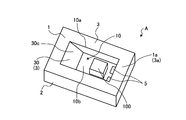
- FIG. 1 is a perspective view showing an example of the light emitting device of this embodiment.
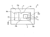
- FIG. 2 is a plan view of the light emitting device shown in FIG.
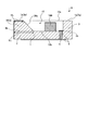
- FIG. 3 is a sectional view taken along the line ii of FIG.
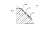
- FIG. 4 is a cross-sectional view of another aspect of the light emitting device.
- FIG. 5 is an enlarged view of FIG.
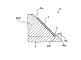
- FIG. 6 is a cross-sectional view of another aspect of the light emitting device.
- FIG. 7 is an enlarged view of FIG.
- FIG. 8 is a cross-sectional view of another aspect of the light emitting device.
- FIG. 9 is an enlarged view of FIG.
- FIG. 10 is a cross-sectional view of another aspect of the light emitting device.
- FIG. 11 is an enlarged view of FIG. FIG.
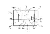
- FIG. 12 is a plan view of another mode of the light emitting device.
- FIG. 13 is a sectional view taken along the line ii-ii in FIG.
- FIG. 14 is a perspective view showing one manufacturing process of the light emitting element housing substrate of the present embodiment.
- FIG. 15 is a cross-sectional view showing one manufacturing process of the light emitting element housing substrate of the present embodiment.
- FIG. 16 is a conceptual diagram showing an optical axis accuracy evaluation device.
- Examples of the light emitting element include a laser diode and a light emitting diode (LED: Light Emitting Diode).
- LED Light Emitting Diode
- the embodiments described below are particularly useful for laser diodes.
- FIG. 1 and 2 are a perspective view and a plan view showing an example of a light emitting device using the light emitting element housing substrate of the present embodiment.
- FIG. 3 is a sectional view taken along the line ii of FIG.
- the light emitting element housing substrate A includes a recess 10 having a bottom surface 10b having an opening 10a in the first surface 1a of the base material 1.
- the base material 1 includes a bottom substrate 2 and side walls 3 arranged on the bottom substrate 2.
- the side wall 3 is adjacent to the recess 10 and exists so as to surround the recess 10.
- the opening 10 a of the recess 10 is at the same height as the first surface 1 a of the base material 1 and forms the end of the recess 10.
- the bottom surface 10b of the recess 10 is at a predetermined depth with respect to the first surface 1a of the base material 1 and forms a part of the surface of the bottom substrate 2.
- a portion of the side wall 3 which forms a part of the first surface 1a of the base material 1 is herein referred to as a first end portion 3a. Further, a portion of the side wall 3, which is located on the opposite side of the first end 3a and serves as a boundary between the side wall 3 and the bottom substrate 2 in the base material 1, is referred to as a second end 3b here. ..
- the first side wall 30 refers to the side wall 3 in which the width LL of the side wall 3 on the bottom face 10b side of the recess 10 is larger than the width HL of the side wall 3 on the opening 10a side of the recess 10.
- the width LL of the side wall 3 on the bottom face 10b side of the recess 10 refers to the length of the second end 3b of the side wall 3 when the substrate 1 is viewed in cross section, as shown in FIG.
- the width HL of the side wall 3 on the side of the opening 10a of the recess 10 refers to the length of the first end 3a of the side wall 3 when the substrate 1 is viewed in cross section.
- a light emitting element 100 such as a laser diode is mounted on the bottom surface 10b of the recess 10.
- the first side wall 30 may be a reflector that reflects light emitted from the light emitting element 100 (hereinafter, also referred to as emitted light).
- a Ni plating film, an Au plating film, or the like may be formed on the inner wall surface 30c of the first side wall 30.
- the light emitting element 100 is mounted on the bottom surface 10b of the recess 10 as described above. Further, at least a part of the side wall 3 (first side wall 30) which is adjacent to the recess 10 and surrounds the recess 10 serves as a reflector for the light emitted from the light emitting element 100.
- the light emitting element housing substrate A has such a structure, when a stress such as a bending moment acts on the reflector (first sidewall 30), the stress is dispersed to the surrounding sidewalls 3. As a result, the deformation of the reflector (first side wall 30) can be reduced. Therefore, the optical axis shift of the reflected light due to the deformation of the reflector (first side wall 30) can be reduced, so that the highly reliable light emitting element housing substrate A can be realized.
- the inner wall surface 30c of the first side wall 30 may be inclined with respect to the bottom surface 10b of the recess 10.
- the first side wall 30 is used as a reflector, for example, the emitted light emitted in parallel to the bottom surface 10b of the recess 10 can be reflected upward.
- “capable of being reflected upward” means that the emitted light is reflected from the bottom surface 10b side of the recess 10 toward the opening 10a side of the recess 10.
- the structure of the first side wall 30 is not limited to a structure in which the width of the first side wall 30 is continuously wider from the opening 10a side of the recess 10 toward the bottom surface 10b side of the recess 10, and various other structures are possible. Is applicable. For example, as described later, the width of the first side wall 30 may be changed stepwise.
- the bottom substrate 2 and the side wall 3 may be integrally formed.
- the stress acting on the reflector (first side wall 30) is dispersed to the bottom substrate 2, so that the deformation of the reflector (first side wall 30) can be reduced more effectively. Therefore, it is possible to realize the substrate A for accommodating the light emitting element with higher reliability.
- the bottom substrate 2 and the side wall 3 may be integrally formed of the same material. In this case, since an interface that causes thermal resistance does not occur between the bottom substrate 2 and the side wall 3, the thermal resistance of the base material 1 can be reduced. Therefore, it is possible to realize the substrate A for housing the light emitting element having high heat dissipation.
- the side wall 3 is preferably present so as to surround the recess 10, but may have a portion around the recess 10 where the side walls 3 are not connected to each other. That is, the end portions of the side wall 3 may be separated from each other. In this case, the side wall 3 preferably surrounds at least half of the outer circumference of the recess 10. Further, the inner wall surface of the side wall 3 may have a corner portion, but may be in a smooth state having no corner portion.
- a ceramic material may be mainly applied to the base material 1 (the bottom substrate 2 and the side wall 3), but a metal material, an organic material, and a glass material may be mainly applied. Further, as described above, the bottom substrate 2 and the side wall 3 may be integrally formed of the same material. Although various ceramics can be applied to the base material 1, aluminum nitride (AlN) may be contained as a main component from the viewpoint of having high thermal conductivity.
- AlN aluminum nitride
- containing aluminum nitride as a main component means that the base material 1 contains aluminum nitride in an amount of 80% by mass or more, and further 90% by mass or more.
- the base material 1 contains aluminum nitride (AlN) as a main component, it is possible to obtain a substrate A for accommodating a light emitting element that is more excellent in heat dissipation.
- via conductors 4 and conductor patterns 5 are provided inside and on the bottom substrate 2 and the side walls 3 as necessary.
- Various metal materials, alloys, and composite materials are applied to the via conductor 4 and the conductor pattern 5.
- the base material 1 contains aluminum nitride (AlN)
- AlN aluminum nitride
- a plating film such as Ni may be formed on the surface of the conductor pattern 5.
- solder or Au—Sn plating film may be provided on the surface of the plating film.
- the light emitting element 100 is bonded onto the bottom surface 10b of the recess 10 using a conductive bonding material such as solder.
- a conductive bonding material such as solder.
- the second electrode (not shown) provided on the upper surface of the light emitting element 100 and the conductor pattern 5 may be electrically connected by wire bonding or the like.
- the first electrode (not shown) provided on the lower surface of the light emitting element 100 and the conductor pattern 5 may be electrically connected to each other via the above-described conductive bonding material.
- FIG. 4 is a sectional view showing an example of a light emitting device using the light emitting element housing substrate of the embodiment.
- the cross-sectional position of FIG. 4 follows the ii cross-section line of FIG.
- FIG. 5 is an enlarged view of the vicinity of the inner wall surface 30c of the first side wall 30 of FIG.
- the light emitting element housing substrate B shown in FIGS. 4 and 5 is a modified form of the above light emitting element housing substrate A, and the common components are denoted by the same reference numerals and detailed description thereof will be omitted.
- the inner wall surface 30c of the first side wall 30 has an inner wall convex portion 6a and an inner wall concave portion 6b.
- the inner wall convex portion 6a becomes a portion in contact with the reflecting mirror 7.
- the inner wall concave portion 6b is a portion that does not contact the reflecting mirror 7.
- a bonding material for bonding the reflection mirror 7 may be filled in the inner wall concave portion 6b and not applied on the inner wall convex portion 6a.
- the reflection mirror 7 can be joined to the inner wall surface 30c of the first side wall 30 in a state of directly contacting a part of the inner wall convex portion 6a, so that the reflection mirror has a high temperature due to the emitted light. 7, heat dissipation to the first side wall 30 can be promoted. As a result, the deformation of the reflection mirror 7 due to the temperature change can be reduced, and thus the optical axis shift of the reflected light can be reduced. Furthermore, since the inner wall recess 6b can be filled with a sufficient amount of the bonding material, the adhesion between the inner wall surface 30c of the first side wall 30 and the reflection mirror 7 can be improved.
- the surface roughness of the inner wall surface 30c of the first side wall 30 may be 1 to 3 ⁇ m.
- the reflecting mirror 7 it is possible to use one in which a dielectric multilayer film is deposited on the surface of a substrate made of metal or glass. Further, as the bonding material, an adhesive material made of resin can be used in addition to the Au—Sn material. When an Au—Sn material is applied, heat resistance can be improved.
- FIG. 6 is a sectional view showing an example of a light emitting device using the light emitting element housing substrate of the embodiment.
- the cross-sectional position of FIG. 6 follows the ii cross-section line of FIG.
- FIG. 7 is an enlarged view of the vicinity of the inner wall surface 30c of the first side wall 30 of FIG.
- the light-emitting element housing substrate C shown in FIGS. 6 and 7 is a modified form of the light-emitting element housing substrate A described above, and common components are denoted by the same reference numerals, and detailed description thereof will be omitted.
- the edge 30d of the inner wall surface 30c of the first side wall 30 on the bottom substrate 2 side is deeper than the bottom surface 10b.
- the bottom substrate 2 has a connection surface 10bb that connects the edge 30d and the bottom surface 10b.
- the inner wall surface 30c of the first side wall 30 and the connection surface 10bb form the groove portion 8.
- the groove 8 forms a part of the recess 10.
- the light emitted from the light emitting element 100 mounted on the bottom surface 10b of the recess 10 can be easily focused on the central portion of the reflecting mirror 7.
- the heat generated by the emitted light is applied to the entire reflection mirror 7. It can be efficiently conducted (released). Therefore, it is possible to prevent the reflection mirror 7 from being locally heated to a high temperature, so that the deformation of the reflection mirror 7 and the deviation of the optical axis of the reflected light can be reduced.
- the inner wall surface 30c of the first side wall 30 and the connection surface 10bb may form a substantially right angle.
- the end of the reflection mirror 7 abuts on the groove portion 8, so that when the reflection mirror 7 is installed on the inner wall surface 30c of the first side wall 30, it can be fixed in a stable state. ..
- the substantially right angle means, for example, 85 ° to 95 °.
- the inner wall surface 30c of the first side wall 30 and the connection surface 10bb are preferably shaped to follow the outer shape of the reflection mirror 7.
- the inner wall surface 30c of the first side wall 30 and the connection surface 10bb may be flat (straight) surfaces.
- FIG. 8 is a sectional view showing an example of a light emitting device using the light emitting element housing substrate of the embodiment.
- the cross-sectional position of FIG. 8 follows the ii cross-section line of FIG.
- FIG. 9 is an enlarged view of the vicinity of the inner wall surface 30c of the first side wall 30 of FIG.
- the light-emitting element housing substrate D shown in FIGS. 8 and 9 is a modified form of the light-emitting element housing substrate A described above, and the common components are denoted by the same reference numerals and detailed description thereof will be omitted.
- the inner wall surface 30c of the first side wall 30 and the bottom surface 10b of the recess 10 form a continuous concave curved surface. That is, the inner wall surface 30c of the first side wall 30 forms a smooth curved surface toward the bottom surface 10b of the recess 10, and the connecting portion SL between the inner wall surface 30c of the first side wall 30 and the bottom surface 10b of the recess 10 has a corner. It does not have a structure. As a result, even when stress is generated in the vicinity of the connecting portion SL, the stress is dispersed in the myriad normal directions of the connecting portion SL, so that the generation of cracks in the first side wall 30 can be suppressed. As a result, when the first side wall 30 forms a reflector for the emitted light, it is possible to reduce the optical axis shift of the reflected light due to the generation of cracks.
- FIG. 10 is a cross-sectional view showing an example of a light emitting device using the light emitting element housing substrate of the embodiment.
- the cross-sectional position in FIG. 10 follows the line ii in FIG.
- FIG. 11 is an enlarged view of the vicinity of the inner wall surface 30c of the first side wall 30 of FIG.
- the light emitting element housing substrate E shown in FIG. 10 and FIG. 11 is a modified form of the above light emitting element housing substrate A, and the common components are denoted by the same reference numerals and detailed description thereof will be omitted.
- a portion of the first side wall 30 that forms a part of the first surface 1a of the base material 1 is referred to as a first end portion 30a here.
- the inner wall surface 30c of the first side wall 30 and the first end portion 30a of the first side wall 30 form a continuous convex curved surface. That is, the inner wall surface 30c of the first side wall 30 forms a smooth curved surface toward the first end portion 30a of the first side wall 30, and the inner wall surface 30c of the first side wall 30 and the first end portion 30a of the first side wall 30.
- the connecting portion SH with and has a structure having no corner portion.
- the first end portion 30a of the first side wall 30 and the lid portion are covered.
- the joint area with the body 9 can be reduced.
- thermal stress acts between the lid 9 and the first side wall 30 due to heating and cooling in seam welding for joining the lid 9 the occurrence of cracks in the first side wall 30 is suppressed. can do.
- the first side wall 30 forms a reflector for the emitted light, it is possible to reduce the optical axis shift of the reflected light due to the generation of cracks.
- FIG. 12 is a plan view showing an example of a light emitting device using the light emitting element housing substrate of the present embodiment.
- FIG. 13 is a sectional view taken along the line ii-ii in FIG.
- the light emitting element housing substrate F shown in FIGS. 12 and 13 is a modified form of the above light emitting element housing substrate A, and the common components are denoted by the same reference numerals, and detailed description thereof will be omitted.
- the outer shape of the base material 1 is a rectangular parallelepiped.
- the base material 1 includes a rectangular parallelepiped bottom substrate 2, and four wall members 33 arranged on the bottom substrate 2 along the four sides of the bottom substrate 2.
- the width TL of the wall member 33 having the first side wall 30 is larger than the width TL of the other wall member 33.
- the width TL of the wall member 33 refers to the length of the first end portion 33a of the wall member 33 when the substrate 1 is viewed in cross section.
- the first end portion 33a refers to a portion of the wall member 33 that forms a part of the first surface 1a of the base material 1.
- the width TL of the wall member 33 having the first side wall 30 is increased, when a stress such as a bending moment acts on the first side wall 30 (reflector), the stress is easily dispersed in the wall member 33.
- the deformation of the first side wall 30 (reflector) can be reduced.
- the optical axis shift of the reflected light due to the deformation of the first side wall 30 (reflector) can be reduced.
- the width of the wall member 33 arranged on the bottom substrate 2 along one side (side X) of the rectangular parallelepiped bottom substrate 2 changes in the direction along the side X, it is constant along the side X.
- the width of the wall member 33 may be measured at each interval, and the average value may be used as the width TL of the wall member 33. In this case, it is preferable to measure the width of the wall member 33 at 10 points or more.
- 14 and 15 are a perspective view and a cross-sectional view showing one manufacturing process of the light emitting element housing substrate A of the embodiment.
- the press die 120 is used to press the green sheet 110 from the upper side to the lower side to form a molded body 130 to be the substrate A for housing the light emitting element.
- a molded body 130 obtained after pressing is processed into a predetermined shape so as to have the recess 10 and the first side wall 30.
- the via conductor is previously formed on at least one of the inside and the surface of the green sheet 110. You may use the green sheet 110 in which 4 and the conductor pattern 5 were formed.
- the formed body 130 is fired (maximum temperature: 1500-1900 ° C.) to obtain a substrate A for housing a light emitting element.
- the light emitting element housing substrates A to F according to each of the above-described embodiments were specifically manufactured, and then the light emitting devices A1 to F1 to which the light emitting element housing substrates A to F were applied were manufactured.
- a mixed powder for forming the green sheet 110 a mixed powder was prepared by mixing yttria powder at 5 mass% and calcia powder at 1 mass% with respect to 94 mass% of aluminum nitride powder.
- an acrylic organic binder and terpineol are appropriately added to a mixed powder obtained by mixing tungsten powder and aluminum nitride powder at a ratio of 7: 3 to prepare a conductor paste, and the via conductor 4 and the conductor pattern 5 are prepared using this.
- a mixed powder obtained by mixing tungsten powder and aluminum nitride powder at a ratio of 7: 3 to prepare a conductor paste, and the via conductor 4 and the conductor pattern 5 are prepared using this.
- the fabricated molded body 130 was fired in a reducing atmosphere for 2 hours under the condition that the maximum temperature was 1800 ° C. to fabricate the substrates A to F for housing light emitting elements.
- the number of samples was 20 for each structure.
- Each of the manufactured light emitting element housing substrates A to F had a shape after firing of length 4 mm ⁇ width 3 mm ⁇ height 1.5 mm. At this time, the side wall 3 had a shape surrounding the recess 10 without a gap.
- a laser diode was mounted on the bottom surface 10b of the recess 10 in each of the manufactured light emitting element housing substrates A to F.
- Au—Sn solder was used to bond the laser diode to the bottom surface 10b of the recess 10.
- a Ni plating film having a thickness of about 5 ⁇ m is formed on the inner wall surface 30c of the first side wall 30, and an Au plating film having a thickness of about 0.1 ⁇ m is further formed.
- the reflector was formed by forming it with a thickness. Separately from this, with respect to each of the ten light emitting element housing substrates A to F, the reflecting mirror 7 was installed on the inner wall surface 30c of the first side wall 30 to form a reflector.
- the reflecting mirror 7 is manufactured by vapor-depositing a dielectric film multilayer film on the surface of a flat plate-shaped substrate made of aluminum, and Au-Sn solder is used to bond it to the inner wall surface 30c of the first side wall 30. I was there.
- the light emitting devices A1 to F1 were manufactured.
- a light emitting device G1 in which a reflector is arranged as a single member on a flat base material was manufactured.
- a light-emitting device H1 in which a reflector is arranged as a single member on a flat plate-shaped substrate and a side wall is arranged so as to surround the reflector and the mounted light-emitting element was manufactured.
- the reflector and the side wall are not integrated, but are formed separately. Further, the width of the side wall was constant in the thickness direction.
- the same materials and manufacturing methods as those of the above light emitting devices A1 to F1 were used.
- ten pieces each having a reflector having a plated film formed thereon and one having a reflector having a reflecting mirror provided thereon were prepared.
- a Kovar cap with a window on the top was joined to each of the light emitting devices A1 to H1.
- Ag—Sn solder was used for such joining, and the atmosphere inside the cap was replaced with He gas.
- a glass plate of a predetermined size coated with an antireflection coating was bonded to the window of the cap with a low melting point glass paste.
- a heat sink made of aluminum was provided on the back surface of each of the light emitting devices A1 to H1 for the purpose of enhancing heat dissipation.
- each of the light emitting devices A1 to H1 was evaluated.
- the accuracy of the optical axis was evaluated using an evaluation device as shown in FIG. Specifically, each of the light emitting devices A1 to H1 is mounted on the substrate 140, electricity is supplied from the outside, and the accuracy of the optical axis is evaluated based on the emitted light emitted to the light receiver 150 3 mm away from the light emitting element 100. did.
- the optical axis shift angle was measured by evaluating the received light intensity distribution of the reflected light 0.1 hour after the light was emitted from the light emitting element 100.
- the received light intensity distribution of the radiated light emitted to the light receiver 150 was evaluated by a PC (Personal Computer) 160 connected to the light receiver 150.
- the light emitting element housing substrates A to H are manufactured so that the emitted light is reflected vertically upward with respect to the mounting surface of the light emitting element 100. That is, in the above-described optical axis accuracy evaluation, when the optical axis of the reflected light is perpendicular to the mounting surface of the light emitting element 100, the optical axis shift angle is 0 °.
- Table 1 shows the results of optical axis accuracy evaluation for each structure. The optical axis accuracy was evaluated both when the reflection mirror 7 was not used and when the reflection mirror 7 was used.
Landscapes
- Physics & Mathematics (AREA)
- Condensed Matter Physics & Semiconductors (AREA)
- General Physics & Mathematics (AREA)
- Electromagnetism (AREA)
- Optics & Photonics (AREA)
- Semiconductor Lasers (AREA)
- Led Device Packages (AREA)
Abstract
本実施形態の一態様に係る発光素子収納用基板(A)は、基材(1)の第1面(1a)に開口部(10a)を備えた、底面(10b)を有する凹部(10)を備えており、凹部(10)に隣接する側壁(3)の少なくとも一部が、凹部(10)の底面(10b)側の幅が凹部(10)の開口部(10a)側の幅よりも大きい第1側壁(30)とされていることを特徴とする。また、本実施形態の発光装置(A1)は、上記の発光素子収納用基板(A)と、凹部(10)の底面(10b)上に搭載されている発光素子(100)とを備えていることを特徴とする。
Description
本開示は、発光素子収納用基板および発光装置に関する。
従来、発光素子を収納するための基板として、発光素子から放射される光を例えば上方に反射させるための反射体を、平板状の基材上に備えている発光素子収納用基板が知られている(例えば、特許文献1を参照)。
本実施形態の一態様に係る発光素子収納用基板は、基材の第1面に開口部を備えた、底面を有する凹部を備えており、該凹部に隣接する側壁の少なくとも一部が、前記底面側の幅が前記開口部側の幅よりも大きい第1側壁とされている。
本実施形態の発光装置は、上記の発光素子収納用基板の前記底面上に発光素子を備えている。
以下、添付図面を参照して、本実施形態の発光素子収納用基板および発光装置の一態様について説明する。ここで、発光素子としては、レーザーダイオード(Laser Diode)および発光ダイオード(LED:Light Emitting Diode)等を挙げることができる。以下に示す各実施形態は、とりわけレーザーダイオード用として有用なものとなる。
図1および図2は、本実施形態の発光素子収納用基板を用いた発光装置の一例を示す斜視図および平面図である。図3は、図2のi-i線断面図である。
図1~図3に示すように、本実施形態に係る発光素子収納用基板Aは、基材1の第1面1aに開口部10aを備えた、底面10bを有する凹部10を備えている。さらに基材1は、底部基板2と、底部基板2上に配置された側壁3とを備えている。側壁3は凹部10に隣接しており、凹部10を囲むように存在している。凹部10の開口部10aは、基材1の第1面1aと等しい高さにあり、凹部10の端部をなしている。凹部10の底面10bは、基材1の第1面1aに対して所定の深さにあり、底部基板2の表面の一部をなしている。側壁3のうち、基材1の第1面1aの一部をなしている部分を、ここでは第1端部3aとする。また、側壁3のうち、第1端部3aの反対側に位置しており、基材1において側壁3と底部基板2との境界となっている部分を、ここでは第2端部3bとする。
発光素子収納用基板Aでは、側壁3の少なくとも一部が第1側壁30とされている。ここで、第1側壁30とは、側壁3において、凹部10の底面10b側における側壁3の幅LLが、凹部10の開口部10a側における側壁3の幅HLよりも大きい側壁をいう。凹部10の底面10b側における側壁3の幅LLとは、図3に示すように、基材1を断面視したときの、側壁3の第2端部3bの長さをいう。また、凹部10の開口部10a側における側壁3の幅HLとは、基材1を断面視したときの、側壁3の第1端部3aの長さをいう。
凹部10の底面10b上には、例えばレーザーダイオード等の発光素子100が搭載される。この場合、第1側壁30は、発光素子100から放射された光(以下、放射光とよぶことがある)を反射させる反射体とすることができる。第1側壁30を反射体とする場合には、第1側壁30の内壁面30c上にNiめっき膜やAuめっき膜等を形成してもよい。
発光素子収納用基板Aでは上述のように、凹部10の底面10b上に発光素子100が搭載される。さらに凹部10に隣接しており、凹部10を囲むように存在している側壁3の少なくとも一部(第1側壁30)を、発光素子100から放射される光の反射体としている。発光素子収納用基板Aがこのような構造を有すると、反射体(第1側壁30)に曲げモーメント等の応力が働いた場合に、その応力が周囲の側壁3に分散される。この結果、反射体(第1側壁30)の変形を低減することができる。したがって、反射体(第1側壁30)の変形による反射光の光軸ずれを低減することができるため、信頼性の高い発光素子収納用基板Aを実現することができる。
発光素子収納用基板Aでは、図3等に示すように、第1側壁30の幅が、凹部10の開口部10a側より、凹部10の底面10b側に向けて連続して広くなっていてもよい。すなわち、第1側壁30の内壁面30cは、凹部10の底面10bに対して傾斜面をなしていてもよい。この場合、第1側壁30を反射体とすれば、例えば凹部10の底面10bに平行に発せられた放射光を上方に反射させることができる。ここで、「上方に反射させることができる」とは、凹部10の底面10b側から、凹部10の開口部10a側に向かう方向に、放射光が反射することをいう。第1側壁30の構造は、第1側壁30の幅が、凹部10の開口部10a側より、凹部10の底面10b側に向けて連続して広くなっているものに限られず、その他種々の構造が適用可能である。例えば後述するように、第1側壁30の幅が段階的に変化する構造であってもよい。
底部基板2と側壁3とは、一体的に形成されていてもよい。この場合、反射体(第1側壁30)に働いた応力が底部基板2まで分散されるようになるため、反射体(第1側壁30)の変形をより効果的に低減することができる。したがって、信頼性のより高い発光素子収納用基板Aを実現することができる。
さらに、底部基板2と側壁3とは、同一の材料により、一体的に形成されていてもよい。この場合、底部基板2と側壁3との間に熱抵抗を生じさせる界面が生じないため、基材1の熱抵抗を小さくすることができる。したがって、放熱性の高い発光素子収納用基板Aを実現することができる。
側壁3は凹部10を囲むように存在しているのがよいが、凹部10の周囲において、側壁3同士がつながっていない部分を有していてもよい。すなわち、側壁3の端部と端部とが離隔された状態であってもよい。この場合側壁3は、凹部10の外周のうち、少なくとも半分以上を囲むものであるとよい。また、側壁3の内壁面は、角をなす部分を有していてもよいが、角部を有さない滑らかな状態であってもよい。
基材1(底部基板2および側壁3)には主として、セラミック材料を適用してもよいが、その他に金属材料、有機材料およびガラス材料を主として適用してもよい。また、上述のように底部基板2および側壁3は同一の材料により一体的に形成されていてもよい。基材1には、種々のセラミックを適用することが可能であるが、高い熱伝導率を有するという点から窒化アルミニウム(AlN)を主成分として含んでいてもよい。
ここで、「窒化アルミニウムを主成分として含んでいる」とは、基材1が窒化アルミニウムを80質量%以上、さらには90質量%以上含んでいることをいう。基材1が窒化アルミニウム(AlN)を主成分として含んでいると、より熱放散性に優れた発光素子収納用基板Aとすることができる。
発光素子収納用基板Aでは必要に応じて、底部基板2および側壁3の内部および表面上にビア導体4および導体パターン5が設けられる。ビア導体4および導体パターン5には、種々の金属材料、合金および複合材料が適用される。基材1が窒化アルミニウム(AlN)を含有する場合には、同時焼成が可能であるという点から、タングステン(W)やモリブデン(Mo)と、窒化アルミニウム(AlN)の複合材料を適用してもよい。導体パターン5の表面には、Niなどのめっき膜を形成してもよい。さらに、かかるめっき膜の表面に、ハンダやAu-Snめっき膜を設けてもよい。
発光素子100は、凹部10の底面10b上にハンダなどの導電性接合材を用いて接合される。この際に、発光素子100の上面に設けられる第2電極(不図示)と、導体パターン5とが、ワイヤボンディングなどで電気的に接続されていてもよい。発光素子100の下面に設けられる第1電極(不図示)と、導体パターン5とが、上記の導電性接合材を介して電気的に接続されていてもよい。
図4は、実施形態の発光素子収納用基板を用いた発光装置の一例を示す断面図である。図4の断面位置は、図2のi-i断面線にならっている。図5は図4の第1側壁30の内壁面30c付近を拡大した図である。図4および図5に示す発光素子収納用基板Bは、上述の発光素子収納用基板Aを変形した形態であり、共通の構成については同一の符号を付して、詳細な説明は省略する。
発光素子収納用基板Bでは、図4および図5に示すように、第1側壁30の内壁面30cが、内壁凸部6aと内壁凹部6bとを有している。
第1側壁30の内壁面30cをこのような構造にすると、例えば反射用ミラー7を第1側壁30の内壁面10c上に設置したときに、内壁凸部6aは反射用ミラー7に接する部分となるが、内壁凹部6bは反射用ミラー7に接しない部分となる。この場合、図示はしていないが、反射用ミラー7を接合するための接合材が内壁凹部6bに充填されて、内壁凸部6a上には塗布されない状態にすることができる。これにより反射用ミラー7を内壁凸部6aの一部に直に接触させた状態で第1側壁30の内壁面30cに接合することが可能になるため、放射光により高温となった反射用ミラー7から、第1側壁30への熱放散を促進することができる。この結果、温度変化に起因する反射用ミラー7の変形を低減することができるため、反射光の光軸ずれを低減することができる。さらに、内壁凹部6bに十分な量の接合材を充填できるため、第1側壁30の内壁面30cと、反射用ミラー7との接着性を向上させることができる。この結果、反射用ミラー7を第1側壁30の内壁面30c上に搭載したときの位置決め精度を向上させることができるため、反射光の光軸ずれを低減することができる。第1側壁30の内壁面30cの表面粗さとしては、1~3μmであってもよい。
反射用ミラー7としては、金属またはガラスからなる基板の表面上に、誘電体多層膜を蒸着させたものを用いることができる。また、接合材としては、Au-Sn材の他、樹脂製の接着材を用いることができる。Au-Sn材を適用した場合、耐熱性を向上させることができる。
図6は、実施形態の発光素子収納用基板を用いた発光装置の一例を示す断面図である。図6の断面位置は、図2のi-i断面線にならっている。図7は図6の第1側壁30の内壁面30c付近を拡大した図である。図6および図7に示す発光素子収納用基板Cは、上述の発光素子収納用基板Aを変形した形態であり、共通の構成については同一の符号を付して、詳細な説明は省略する。
発光素子収納用基板Cでは、図6および図7に示すように、第1側壁30の内壁面30cにおける、底部基板2側の端縁30dが、底面10bに対して深い位置にある。この場合、底部基板2は、端縁30dと底面10bとをつなぐ、接続面10bbを有している。そして、第1側壁30の内壁面30cと、接続面10bbとが、溝部8を形成している。この場合溝部8は、凹部10の一部をなしている。溝部8が形成されていると、反射用ミラー7の端部が、凹部10の底面10bよりも深い位置をとるように、反射用ミラー7を設置できる。この結果、凹部10の底面10b上に搭載された発光素子100から放射される光を、反射用ミラー7の中心部に集光させやすくなる。放射光を反射用ミラー7の中心部に集光させる場合には、放射光を反射用ミラー7の端部に集光させる場合に比べて、放射光により発生する熱を反射用ミラー7全体に効率よく伝導させる(逃がす)ことができる。したがって、反射用ミラー7が局所的に高温となることを防ぐことができるため、反射用ミラー7の変形および反射光の光軸ずれを低減することができる。
溝部8において、第1側壁30の内壁面30cと、接続面10bbとは、略直角をなしていてもよい。この場合、反射用ミラー7の端部が、溝部8に突き当たる状態となるため、反射用ミラー7を第1側壁30の内壁面30c上に設置したときに、安定した状態で固定することができる。これにより反射用ミラー7を第1側壁30の内壁面30c上に搭載したときの位置決め精度を向上させることができるため、反射光の光軸ずれを低減することができる。ここで略直角とは、例えば85°~95°のことをいう。この場合、第1側壁30の内壁面30cおよび接続面10bbは、反射用ミラー7の外形に沿う形状であるとよい。例えば、第1側壁30の内壁面30cおよび接続面10bbは、平坦(まっすぐ)な面であるとよい。
図8は、実施形態の発光素子収納用基板を用いた発光装置の一例を示す断面図である。図8の断面位置は、図2のi-i断面線にならっている。図9は図8の第1側壁30の内壁面30c付近を拡大した図である。図8および図9に示す発光素子収納用基板Dは、上述の発光素子収納用基板Aを変形した形態であり、共通の構成については同一の符号を付して、詳細な説明は省略する。
発光素子収納用基板Dでは、図8および図9に示すように、第1側壁30の内壁面30cと、凹部10の底面10bとが連続した凹状の湾曲面を成している。すなわち、第1側壁30の内壁面30cは凹部10の底面10bにかけて滑らかな曲面をなしており、第1側壁30の内壁面30cと凹部10の底面10bとの接続部SLが角部を有していない構造となっている。これにより接続部SL付近において応力が発生した場合にも、接続部SLの無数の法線方向に応力が分散されるため、第1側壁30におけるクラックの発生を抑制することができる。この結果、第1側壁30が放射光に対する反射体を成す場合に、クラックの発生による反射光の光軸ずれを低減することができる。
図10は、実施形態の発光素子収納用基板を用いた発光装置の一例を示す断面図である。図10の断面位置は、図2のi-i断面線にならっている。図11は図10の第1側壁30の内壁面30c付近を拡大した図である。図10および図11に示す発光素子収納用基板Eは、上述の発光素子収納用基板Aを変形した形態であり、共通の構成については同一の符号を付して、詳細な説明は省略する。
図10および図11に示す発光素子収納用基板Eにおいて、第1側壁30のうち、基材1の第1面1aの一部をなしている部分を、ここでは第1端部30aとする。発光素子収納用基板Eでは、第1側壁30の内壁面30cと、第1側壁30の第1端部30aとが連続した凸状の曲面をなしている。すなわち、第1側壁30の内壁面30cは第1側壁30の第1端部30aにかけて滑らかな曲面をなしており、第1側壁30の内壁面30cと、第1側壁30の第1端部30aとの接続部SHが角部を有していない構造となっている。この場合、例えば第1側壁30の第1端部30a上に蓋体9を接合する際に、接続部SHが角部を有する場合に比べて、第1側壁30の第1端部30aと蓋体9との接合面積を小さくすることができる。これにより、蓋体9を接合するためのシーム溶接における加熱および冷却等により、蓋体9と第1側壁30との間に熱応力が働いた場合に、第1側壁30におけるクラックの発生を抑制することができる。この結果、第1側壁30が放射光に対する反射体を成す場合に、クラックの発生による反射光の光軸ずれを低減することができる。
図12は、本実施形態の発光素子収納用基板を用いた発光装置の一例を示す平面図である。図13は、図12のii-ii線断面図である。図12および図13に示す発光素子収納用基板Fは、上述の発光素子収納用基板Aを変形した形態であり、共通の構成については同一の符号を付して、詳細な説明は省略する。
発光素子収納用基板Fでは、図12および図13に示すように、基材1の外形が直方体状となっている。さらに基材1は直方体状の底部基板2と、底部基板2の4辺に沿って、底部基板2上に配置された4つの壁部材33とを備えている。そして、図13等に示すように、第1側壁30を有している壁部材33の幅TLは、他の壁部材33の幅TLよりも大きくなっている。ここで壁部材33の幅TLとは、基材1を断面視したときの、壁部材33の第1端部33aの長さをいう。この場合、第1端部33aとは、壁部材33のうち、基材1の第1面1aの一部をなしている部分をいう。
第1側壁30を有している壁部材33の幅TLを大きくした場合、第1側壁30(反射体)に曲げモーメント等の応力が働いた場合に、壁部材33に応力が分散されやすくなり、第1側壁30(反射体)の変形を低減することができる。この結果、第1側壁30(反射体)の変形による反射光の光軸ずれを低減することができる
直方体状の底部基板2の1辺(辺X)に沿って、底部基板2上に配置された壁部材33の幅が、辺Xに沿う方向で変化する場合には、辺Xに沿って一定間隔毎に壁部材33の幅を計測し、その平均値を壁部材33の幅TLとしてもよい。この場合、壁部材33の幅を10点以上計測するのがよい。
次に、各実施形態に係る発光素子収納用基板の製造方法について説明する。図14および図15は、実施形態の発光素子収納用基板Aの一製造工程を示す斜視図および断面図である。
まず、あらかじめ直方体型に加工したグリーンシート110を用意する。次に、プレス金型120を用いて、グリーンシート110の上方から下方に向けてプレス加工を行い、発光素子収納用基板Aとなる成形体130を形成する。プレス金型120は、プレス後に得られる成形体130が、凹部10および第1側壁30を有するように所定の形状に加工されている。
なお、内部および表面上の少なくとも一方に、ビア導体4および導体パターン5を有する発光素子収納用基板Aを作成する場合には、グリーンシート110の内部および表面上の少なくとも一方に、予め、ビア導体4および導体パターン5を形成したグリーンシート110を用いてもよい。
次に、作成した成形体130を焼成(最高温度:1500-1900℃)して、発光素子収納用基板Aを得る。
以上、本開示の実施形態について説明したが、本開示は上記実施形態に限定されるものではなく、その趣旨を逸脱しない限りにおいて種々の変更が可能である。
以下、上述の各実施形態に係る発光素子収納用基板A~Fを具体的に作製し、次いで、かかる発光素子収納用基板A~Fを適用した発光装置A1~F1を作製した。
まず、グリーンシート110を形成するための混合粉末として、窒化アルミニウム粉末94質量%に対して、イットリア粉末を5質量%、カルシア粉末を1質量%の割合で混合した混合粉末を調製した。
次に、この混合粉末100質量部に対して、有機バインダーとしてアクリル系バインダーを20質量部、トルエンを50質量部添加してスラリーを調製し、次に、ドクターブレード法を用いて所定の厚みのグリーンシート110を作製した。
次に、タングステン粉末と窒化アルミニウム粉末を7:3の比率で混合した混合粉末に、アクリル系有機バインダーおよびテルピネオールを適宜添加して導体ペーストを調製し、これを用いてビア導体4および導体パターン5をグリーンシート110に形成した。
そして、上述のグリーンシート110を用いて、図14等に示した製造方法によって成形体130を作製した。
作製した成形体130を、還元雰囲気中、最高温度が1800℃となる条件にて2時間の焼成を行って発光素子収納用基板A~Fを作製した。試料数は各構造に対して20個ずつとした。
作製した各発光素子収納用基板A~Fは、焼成後の形状で長さ4mm×幅3mm×高さ1.5mmであった。このとき、側壁3は凹部10を隙間なく囲む形状をなしていた。
次に、作製した各発光素子収納用基板A~Fにおける、凹部10の底面10b上にレーザーダイオードを実装した。ここで、凹部10の底面10bへのレーザーダイオードの接合には、Au-Snハンダを用いた。
次に、10個の各発光素子収納用基板A~Fについて、第1側壁30の内壁面30c上に、Niめっき膜を約5μmの厚みで形成し、さらにAuめっき膜を約0.1μmの厚みで形成することで、反射体を形成した。これとは別に、10個の各発光素子収納用基板A~Fについて、第1側壁30の内壁面30c上に反射用ミラー7を設置することで、反射体を形成した。反射用ミラー7は、アルミニウムからなる平板状の基板の表面上に、誘電体膜多層膜を蒸着させることにより作製し、第1側壁30の内壁面30cとの接合にはAu-Snハンダを用いた。
このようにして、発光装置A1~F1を作製した。
次に比較例として、平板状の基材上に単独の部材として反射体が配置されている発光装置G1を作製した。また、平板状の基材上に、単独の部材として反射体が配置されており、さらに反射体および搭載された発光素子を囲むように側壁が配置されている発光装置H1を作製した。なお発光装置H1においては、反射体と側壁とは一体化しておらず、別々に形成されている。また、側壁の幅は厚み方向に一定とした。発光装置G1および発光装置H1の作製にあたっては、上述の発光装置A1~F1と同様の材料・製法を用いた。このとき、発光装置G1および発光装置H1についても、めっき膜を形成した反射体を有するものと、反射用ミラーを設置した反射体を有するものとを、各10個ずつ作製した。
次に、各発光装置A1~H1に、上面に窓が付いたコバール製のキャップを接合した。ここで、かかる接合にはAg-Snハンダを用い、キャップの内部雰囲気はHeガスで置換した。また、キャップの窓には、反射防止コートを施した所定のサイズのガラス板を、低融点ガラスペーストにより接合した。
次に、各発光装置A1~H1の裏面に、熱放散性を高める用途でアルミニウムからなるヒートシンクを設けた。
次に、各発光装置A1~H1の光軸の精度について評価した。かかる光軸の精度については、図16に示すような評価装置を用いて評価した。具体的には、各発光装置A1~H1を基板140に実装して外部から電気を供給し、発光素子100から3mm離れた受光器150に放射された放射光に基づいて光軸の精度を評価した。
光軸の精度評価にあたっては、発光素子100から光が放射され始めてから0.1時間後の、反射光の受光強度分布を評価することで光軸ずれ角を測定した。なお、受光器150に放射された放射光の受光強度分布は、かかる受光器150に接続されるPC(Personal Computer)160で評価した。
なお、各発光装置A1~H1では、放射光が発光素子100の搭載面に対して垂直上方に反射されるように、発光素子収納用基板A~Hを作製している。すなわち上述の光軸精度評価では、反射光の光軸が発光素子100の搭載面に対して垂直であるときに、光軸ずれ角は0°とされる。
各構造における、光軸精度評価の結果を表1に示す。なお、光軸精度評価は、反射用ミラー7を使用しない場合と、反射用ミラー7を使用する場合の双方で行った。

平板状の基材上に単独の部材として反射体が配置されている発光装置G1と、平板状の基材上に、単独の部材として反射体が配置されており、さらに反射体および搭載された発光素子を囲むように側壁が配置されている発光装置H1との間においては、発生した光軸ずれ角に有意差は確認できなかった。
発光装置G1および発光装置H1と、上述の各実施形態に係る発光装置A1~F1との比較においては、本実施形態に係る発光装置A1~F1(発光素子収納用基板A~F)では、光軸ずれを低減できることが分かる。
A~F 発光素子収納用基板
1 基材
2 底部基板
3 側壁
30 第1側壁
4 ビア導体
5 導体パターン
6a 内壁凸部
6b 内壁凹部
7 反射用ミラー
8 溝部
9 蓋体
10 凹部
100 発光素子
110 グリーンシート
120 プレス金型
130 成形体
140 (光軸精度評価用)基板
150 (光軸精度評価用)受光器
160 (光軸精度評価用)PC
1 基材
2 底部基板
3 側壁
30 第1側壁
4 ビア導体
5 導体パターン
6a 内壁凸部
6b 内壁凹部
7 反射用ミラー
8 溝部
9 蓋体
10 凹部
100 発光素子
110 グリーンシート
120 プレス金型
130 成形体
140 (光軸精度評価用)基板
150 (光軸精度評価用)受光器
160 (光軸精度評価用)PC
Claims (8)
- 基材の第1面に開口部を備えた、底面を有する凹部を備えており、
該凹部に隣接する側壁の少なくとも一部が、前記底面側の幅が前記開口部側の幅よりも大きい第1側壁とされている、発光素子収納用基板。 - 前記第1側壁の幅が、前記開口部側より前記底面側に向けて連続して広くなっている、請求項1に記載の発光素子収納用基板。
- 前記第1側壁の内壁面が、凹凸部を有している、請求項1に記載の発光素子収納用基板。
- 前記第1側壁の前記底面側の端縁は、前記底面よりも深い位置にある、請求項1乃至3のいずれか一つに記載の発光素子収納用基板。
- 前記第1側壁の内壁面と、前記底面とが連続した凹状の湾曲面を成している、請求項1乃至3のいずれか一つに記載の発光素子収納用基板。
- 前記第1側壁は、内壁面と上面とが連続した凸状の湾曲面を成している、請求項1乃至5のいずれか一つに記載の発光素子収納用基板。
- 前記基材は、外形が直方体状であり、前記底面を有する底部基板と、該底部基板の4辺に沿って配置される4つの壁部材と、を備え、
4つの前記壁部材のうち、前記第1側壁を有する前記壁部材の幅が、他の前記壁部材の幅よりも大きい、請求項1乃至6のいずれか一つに記載の発光素子収納用基板。 - 請求項1乃至7のいずれか一つに記載の発光素子収納用基板の前記底面上に発光素子を備えている、発光装置。
Priority Applications (1)
| Application Number | Priority Date | Filing Date | Title |
|---|---|---|---|
| JP2020556591A JP7122392B2 (ja) | 2018-11-08 | 2019-07-17 | 発光素子収納用基板および発光装置 |
Applications Claiming Priority (2)
| Application Number | Priority Date | Filing Date | Title |
|---|---|---|---|
| JP2018-210661 | 2018-11-08 | ||
| JP2018210661 | 2018-11-08 |
Publications (1)
| Publication Number | Publication Date |
|---|---|
| WO2020095481A1 true WO2020095481A1 (ja) | 2020-05-14 |
Family
ID=70610851
Family Applications (1)
| Application Number | Title | Priority Date | Filing Date |
|---|---|---|---|
| PCT/JP2019/028171 Ceased WO2020095481A1 (ja) | 2018-11-08 | 2019-07-17 | 発光素子収納用基板および発光装置 |
Country Status (2)
| Country | Link |
|---|---|
| JP (1) | JP7122392B2 (ja) |
| WO (1) | WO2020095481A1 (ja) |
Citations (7)
| Publication number | Priority date | Publication date | Assignee | Title |
|---|---|---|---|---|
| JP2004031708A (ja) * | 2002-06-26 | 2004-01-29 | Citizen Electronics Co Ltd | 半導体レーザーパッケージ |
| JP2008518461A (ja) * | 2004-10-25 | 2008-05-29 | クリー インコーポレイテッド | 固体金属ブロック半導体発光デバイス実装基板ならびにキャビティおよびヒートシンクを含むパッケージ、ならびにそれらをパッケージングする方法 |
| JP2010093066A (ja) * | 2008-10-08 | 2010-04-22 | Sanyo Electric Co Ltd | 発光装置 |
| JP2011228137A (ja) * | 2010-04-20 | 2011-11-10 | Panasonic Corp | 照明装置及び表示装置 |
| DE102015108117A1 (de) * | 2015-05-22 | 2016-11-24 | Osram Opto Semiconductors Gmbh | Bauelement |
| WO2017183638A1 (ja) * | 2016-04-18 | 2017-10-26 | 京セラ株式会社 | 発光素子収納用部材、アレイ部材および発光装置 |
| CN108321282A (zh) * | 2018-04-03 | 2018-07-24 | 江苏鸿利国泽光电科技有限公司 | 一种紫外led封装器件 |
-
2019
- 2019-07-17 JP JP2020556591A patent/JP7122392B2/ja active Active
- 2019-07-17 WO PCT/JP2019/028171 patent/WO2020095481A1/ja not_active Ceased
Patent Citations (7)
| Publication number | Priority date | Publication date | Assignee | Title |
|---|---|---|---|---|
| JP2004031708A (ja) * | 2002-06-26 | 2004-01-29 | Citizen Electronics Co Ltd | 半導体レーザーパッケージ |
| JP2008518461A (ja) * | 2004-10-25 | 2008-05-29 | クリー インコーポレイテッド | 固体金属ブロック半導体発光デバイス実装基板ならびにキャビティおよびヒートシンクを含むパッケージ、ならびにそれらをパッケージングする方法 |
| JP2010093066A (ja) * | 2008-10-08 | 2010-04-22 | Sanyo Electric Co Ltd | 発光装置 |
| JP2011228137A (ja) * | 2010-04-20 | 2011-11-10 | Panasonic Corp | 照明装置及び表示装置 |
| DE102015108117A1 (de) * | 2015-05-22 | 2016-11-24 | Osram Opto Semiconductors Gmbh | Bauelement |
| WO2017183638A1 (ja) * | 2016-04-18 | 2017-10-26 | 京セラ株式会社 | 発光素子収納用部材、アレイ部材および発光装置 |
| CN108321282A (zh) * | 2018-04-03 | 2018-07-24 | 江苏鸿利国泽光电科技有限公司 | 一种紫外led封装器件 |
Also Published As
| Publication number | Publication date |
|---|---|
| JPWO2020095481A1 (ja) | 2021-09-30 |
| JP7122392B2 (ja) | 2022-08-19 |
Similar Documents
| Publication | Publication Date | Title |
|---|---|---|
| US8178895B2 (en) | Semiconductor light-emiting device and method | |
| CN110094643B (zh) | 发光装置 | |
| JP7508198B2 (ja) | 発光装置およびその製造方法 | |
| JP6893781B2 (ja) | 発光素子搭載用パッケージおよび発光装置 | |
| CN105849922A (zh) | 用于相机的薄的led闪光灯 | |
| CN109075526B (zh) | 发光元件收纳用构件及发光装置 | |
| JP2017117880A (ja) | 光素子搭載用パッケージ、光素子搭載用母基板および電子装置 | |
| WO2019163987A1 (ja) | 電子部品搭載用パッケージ、電子装置および電子モジュール | |
| CN112636160B (zh) | 激光器 | |
| JP2004327632A (ja) | 発光素子収納用パッケージおよび発光装置 | |
| US20150187838A1 (en) | Light emitting device and method of manufacturing the same | |
| JP4818028B2 (ja) | 発光素子搭載用基板、発光素子収納用パッケージ、発光装置および照明装置 | |
| JP2005174998A (ja) | 発光素子収納用パッケージおよび発光装置 | |
| JP7122392B2 (ja) | 発光素子収納用基板および発光装置 | |
| US11955769B2 (en) | Optical element mounting package, electronic device, and electronic module | |
| JP5393419B2 (ja) | 発光素子搭載用基板および発光装置 | |
| CN110808321A (zh) | 紫外光led封装结构 | |
| CN113711349B (zh) | 发光元件搭载用基板以及发光装置 | |
| JP7399180B2 (ja) | 光素子搭載用パッケージ、電子装置及び電子モジュール | |
| JP2013172002A (ja) | 配線基板および発光装置 | |
| KR100862515B1 (ko) | 발광소자 패키지 | |
| JP7228433B2 (ja) | 照明装置 | |
| JP7148276B2 (ja) | 発光素子搭載用パッケージおよび発光装置 | |
| JP4480736B2 (ja) | 発光装置 | |
| WO2020066780A1 (ja) | 発光素子搭載用基板、アレイ基板および発光装置 |
Legal Events
| Date | Code | Title | Description |
|---|---|---|---|
| 121 | Ep: the epo has been informed by wipo that ep was designated in this application |
Ref document number: 19882428 Country of ref document: EP Kind code of ref document: A1 |
|
| ENP | Entry into the national phase |
Ref document number: 2020556591 Country of ref document: JP Kind code of ref document: A |
|
| NENP | Non-entry into the national phase |
Ref country code: DE |
|
| 122 | Ep: pct application non-entry in european phase |
Ref document number: 19882428 Country of ref document: EP Kind code of ref document: A1 |