WO2020090496A1 - 電子機器 - Google Patents
電子機器 Download PDFInfo
- Publication number
- WO2020090496A1 WO2020090496A1 PCT/JP2019/040869 JP2019040869W WO2020090496A1 WO 2020090496 A1 WO2020090496 A1 WO 2020090496A1 JP 2019040869 W JP2019040869 W JP 2019040869W WO 2020090496 A1 WO2020090496 A1 WO 2020090496A1
- Authority
- WO
- WIPO (PCT)
- Prior art keywords
- housing
- electronic device
- wiring board
- opening
- energy harvesting
- Prior art date
- Legal status (The legal status is an assumption and is not a legal conclusion. Google has not performed a legal analysis and makes no representation as to the accuracy of the status listed.)
- Ceased
Links
Images


Classifications
-
- H—ELECTRICITY
- H01—ELECTRIC ELEMENTS
- H01R—ELECTRICALLY-CONDUCTIVE CONNECTIONS; STRUCTURAL ASSOCIATIONS OF A PLURALITY OF MUTUALLY-INSULATED ELECTRICAL CONNECTING ELEMENTS; COUPLING DEVICES; CURRENT COLLECTORS
- H01R12/00—Structural associations of a plurality of mutually-insulated electrical connecting elements, specially adapted for printed circuits, e.g. printed circuit boards [PCB], flat or ribbon cables, or like generally planar structures, e.g. terminal strips, terminal blocks; Coupling devices specially adapted for printed circuits, flat or ribbon cables, or like generally planar structures; Terminals specially adapted for contact with, or insertion into, printed circuits, flat or ribbon cables, or like generally planar structures
- H01R12/70—Coupling devices
- H01R12/71—Coupling devices for rigid printing circuits or like structures
- H01R12/72—Coupling devices for rigid printing circuits or like structures coupling with the edge of the rigid printed circuits or like structures
- H01R12/73—Coupling devices for rigid printing circuits or like structures coupling with the edge of the rigid printed circuits or like structures connecting to other rigid printed circuits or like structures
-
- H—ELECTRICITY
- H05—ELECTRIC TECHNIQUES NOT OTHERWISE PROVIDED FOR
- H05K—PRINTED CIRCUITS; CASINGS OR CONSTRUCTIONAL DETAILS OF ELECTRIC APPARATUS; MANUFACTURE OF ASSEMBLAGES OF ELECTRICAL COMPONENTS
- H05K7/00—Constructional details common to different types of electric apparatus
- H05K7/14—Mounting supporting structure in casing or on frame or rack
-
- H—ELECTRICITY
- H02—GENERATION; CONVERSION OR DISTRIBUTION OF ELECTRIC POWER
- H02S—GENERATION OF ELECTRIC POWER BY CONVERSION OF INFRARED RADIATION, VISIBLE LIGHT OR ULTRAVIOLET LIGHT, e.g. USING PHOTOVOLTAIC [PV] MODULES
- H02S40/00—Components or accessories in combination with PV modules, not provided for in groups H02S10/00 - H02S30/00
- H02S40/30—Electrical components
- H02S40/34—Electrical components comprising specially adapted electrical connection means to be structurally associated with the PV module, e.g. junction boxes
-
- Y—GENERAL TAGGING OF NEW TECHNOLOGICAL DEVELOPMENTS; GENERAL TAGGING OF CROSS-SECTIONAL TECHNOLOGIES SPANNING OVER SEVERAL SECTIONS OF THE IPC; TECHNICAL SUBJECTS COVERED BY FORMER USPC CROSS-REFERENCE ART COLLECTIONS [XRACs] AND DIGESTS
- Y02—TECHNOLOGIES OR APPLICATIONS FOR MITIGATION OR ADAPTATION AGAINST CLIMATE CHANGE
- Y02E—REDUCTION OF GREENHOUSE GAS [GHG] EMISSIONS, RELATED TO ENERGY GENERATION, TRANSMISSION OR DISTRIBUTION
- Y02E10/00—Energy generation through renewable energy sources
- Y02E10/50—Photovoltaic [PV] energy
Definitions
- the present invention relates to electronic devices.
- a solar cell module including a solar cell that generates electric power by using light energy such as sunlight is cited.
- the electronic device can be operated with the power supplied from the energy harvesting module, which is convenient.
- Patent Document 1 discloses a configuration in which an output terminal of a solar cell and an input terminal of a printed circuit board are pressure-bonded to a conductive member having elasticity to mechanically and electrically connect the solar cell and the printed circuit board. Has been done.
- Patent Document 1 Since the configuration described in Patent Document 1 is a configuration in which the output terminal of the solar cell and the input terminal of the printed circuit board are crimped to the conductive member, it is necessary to fix the solar cell and the printed circuit board in predetermined positions. However, it has not been possible to easily connect the solar cell and the printed circuit board mechanically and electrically.
- an object of the present invention is to solve the above-mentioned problems and to provide an electronic device that can easily and mechanically and electrically connect an energy harvesting module and a wiring board.
- An object of the present invention is to advantageously solve the above problems, and an electronic device of the present invention is an electronic device that is mechanically and electrically removable from an external energy harvesting module.
- the connector of the energy harvesting module can be inserted into the first opening of the second housing, and the connector of the energy harvesting module and the wiring can be connected through the terminal.
- the substrate can be mechanically and electrically connected. Therefore, the electronic device of the present invention can easily mechanically and electrically connect the energy harvesting module and the wiring board.
- the second housing further includes a third opening adjacent to the first opening, and the connector is inserted into the first opening in the third opening.
- the connector is inserted into the first opening in the third opening.
- the thin plate-shaped energy harvesting panel is stably held in the second housing, so that it is possible to reduce the risk of damage to the peripheral portion of the energy harvesting panel adjacent to the connector.
- the first housing has a linear edge portion.
- a support plate arranged on the same surface as the surface of the wiring board on which the terminals are arranged is further provided, and the support plate has the second housing with respect to the terminals. It is preferably located on the side opposite to.
- the first housing and the second housing are integrally formed. With such a structure, the strength of the electronic device can be improved.
- the load circuit is a light emitting element.
- the user can enjoy the light emission of the light emitting element by the electric power supplied from the energy harvesting module.
- an electronic device capable of easily mechanically and electrically connecting the energy harvesting module and the wiring board.
- FIG. 3 is a perspective view showing a schematic configuration of a first housing and a second housing as viewed from the X-axis positive direction side. It is the perspective view seen from the X-axis negative direction side showing the schematic structure of the 1st housing and the 2nd housing. It is a top view which shows the state in which the energy harvesting module was attached to the electronic device. It is a top view which shows schematic structure of the electronic device which concerns on a 1st modification. It is the figure which looked at the wiring board etc. in the electronic device concerning the 2nd modification from the Z-axis negative direction side.
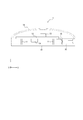
- FIG. 1 is a side view showing a schematic configuration of an electronic device 1 according to an embodiment of the present invention.
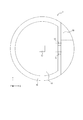
- FIG. 2 is a top view of the electronic device 1 according to the embodiment of the present invention.
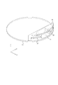
- FIG. 3 is a perspective view of the first housing 10 and the second housing 20 shown in FIGS. 1 and 2 as viewed from the X-axis positive direction side.
- FIG. 4 is a perspective view of the first housing 10 and the second housing 20 shown in FIGS. 1 and 2 as viewed from the X-axis negative direction side.
- the electronic device 1 is an electronic device to which an external energy harvesting module can be attached mechanically and electrically.
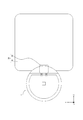
- FIG. 5 shows a top view of a state in which the energy harvesting module 30 is mounted on the electronic device 1.
- the electronic device 1 is equipped with the environmental power generation module 30, the generated electric power can be supplied from the environmental power generation module 30.
- the energy harvesting module 30 will be described as having a solar cell that uses light energy such as sunlight and indoor light to generate electricity. It may have a thermoelectric conversion element that generates electric power using thermal energy.
- the energy harvesting module 30 includes an energy harvesting panel 31 and a connector 32.
- the energy harvesting panel 31 has a thin plate shape.
- the energy harvesting panel 31 has a solar cell that uses light energy such as sunlight and room light to generate electricity.
- the connector 32 outputs the power generated by the energy harvesting panel 31.
- the connector 32 may be a male connector.
- the connector 32 has an output terminal capable of outputting generated power at its tip.
- the electronic device 1 includes a first housing 10, a second housing 20, a supporting portion 11, a wiring board 12, a load circuit 13, a secondary battery 14, and a terminal 15. And a cover 16.
- FIG. 1 in order to visualize the internal structure of the electronic device 1, the side surface of the electronic device 1 is shown assuming that the cover 16 is transparent. In the top view of the electronic device 1 shown in FIG. 2, the cover 16 is omitted.
- the first housing 10 has a disc shape in the examples shown in FIGS. 1 and 2.
- the first housing 10 is not limited to the disk-like shape, and may have any shape including a flat plate-shaped portion.
- the first housing 10 may have, for example, engaging means for engaging with the cover 16 on the surface of the flat plate portion.
- the engagement means may be, for example, a claw, a notch, a groove, or the like.
- the second housing 20 is arranged on the first housing 10.
- the second housing 20 is fitted with the connector 32 of the energy harvesting module 30 when the energy harvesting module 30 shown in FIG. 5 is mounted on the electronic device 1.
- the connector 32 which is a male connector, may be inserted into the second housing 20.
- the second housing 20 may be formed integrally with the first housing 10. Since the first housing 10 and the second housing 20 are integrally formed, the strength of the electronic device 1 can be improved.
- the second housing 20 has a first opening 21 on the outer surface (the surface on the positive side in the X-axis direction).
- the connector 32 of the energy harvesting module 30 can be inserted into the first opening 21 when the energy harvesting module 30 is attached to the electronic device 1. By inserting / removing the connector 32 through the first opening 21, the energy harvesting module 30 can be mechanically attached / detached to / from the electronic device 1.
- the shape of the first opening 21 is a shape adapted to the connector 32, and when the connector 32 is inserted through the first opening 21, the second housing 20 and the connector 32 are fitted together.
- the second housing 20 may be fitted to the entire connector 32 or a part of the connector 32.
- the second housing 20 has a second opening 22 on the surface opposite to the surface on which the first opening 21 is provided (X-axis negative direction side surface).
- the second housing 20 penetrates from the first opening 21 toward the second opening 22.
- the connector 32 of the energy harvesting module 30 can be electrically connected to the terminal 15 shown in FIGS. 1 and 2 through the second opening 22.
- the second housing 20 has two third opening portions 23 adjacent to the first opening portion 21 on the outer surface (surface on the X-axis positive direction side). As shown in FIG. 3, the open portions of the first opening 21 and the third opening 23 are connected to each other.
- the peripheral edge of the energy harvesting panel 31 adjacent to the connector 32 is inserted into the third opening 23. Accordingly, the third opening 23 can hold the thin plate-shaped energy harvesting panel 31 when the connector 32 is inserted into the first opening 21. Since the third opening 23 holds the peripheral portion of the energy harvesting panel 31, the electronic device 1 can stably hold the energy harvesting module 30. In addition, the electronic device 1 can reduce the risk that the peripheral portion of the energy harvesting panel 31 adjacent to the connector 32 is damaged.
- Engaging means capable of engaging with the connector 32 may be provided on the inner wall of the second housing 20.
- the engagement means may be, for example, a claw, a notch, a groove, or the like. With such an engaging means, the second housing 20 and the connector 32 can be fitted more firmly.
- the inner wall of the second housing 20 may be partially covered with an elastic material such as rubber.
- the elastic material functions as a packing, and it is possible to prevent water from entering the inside of the electronic device 1 from the first opening 21.
- the support portion 11 has a columnar shape and extends from the upper surface (the surface on the Z axis positive direction side) of the first housing 10 in the Z axis positive direction.
- the support portion 11 is fixed to the first housing 10.
- the support portion 11 may be formed integrally with the first housing 10.
- the supporting portion 11 supports the wiring board 12.
- the support portion 11 may support the wiring board 12 so that the wiring board 12 is substantially parallel to the first housing 10.
- the support portion 11 may support the wiring board 12 by an engaging means such as a screw or a bolt.
- the wiring board 12 is supported by the support portion 11 and arranged above the first housing 10.
- a load circuit 13, a secondary battery 14, and a terminal 15 are arranged on the wiring board 12.
- the load circuit 13, the secondary battery 14, and the terminal 15 are electrically connected to each other via wiring in the wiring board 12.
- the wiring board 12 is arranged side by side with the second housing 20 in the lateral direction (X-axis direction). As described above, since the wiring boards 12 are not stacked on the second housing 20, the electronic device 1 can be thinned in the Z-axis direction. Therefore, the electronic device 1 can be downsized.
- the load circuit 13 is arranged on the wiring board 12.
- the load circuit 13 can receive power from the energy harvesting module 30 via the terminal 15 and the wiring in the wiring board 12. Further, the load circuit 13 can be supplied with electric power from the secondary battery 14 via the wiring in the wiring board 12. The load circuit 13 can consume the electric power supplied from the energy harvesting module 30 or the secondary battery 14.
- the load circuit 13 may be, for example, a light emitting element such as an LED (Light Emitting Diode) or a speaker.
- the secondary battery 14 is arranged on the wiring board 12.
- the secondary battery 14 is a chargeable / dischargeable secondary battery.
- the secondary battery 14 is, for example, a lithium ion battery or a nickel hydrogen battery.
- the secondary battery 14 receives power from the energy harvesting module 30 via the terminal 15 and the wiring in the wiring board 12, and stores the power. You can
- the stored electric power can be supplied to the load circuit 13.
- the electronic device 1 supplies the electric power to the load circuit 13 in a compact state in which the energy harvesting module 30 is detached. Can be supplied.
- the electronic device 1 can use the power generated by the energy harvesting module 30 having an area equal to or larger than the housing of the electronic device 1.
- the terminal 15 is made of a conductive material.
- the conductive material include metal materials selected from the group consisting of copper, aluminum, nickel and iron, and alloy materials containing these metal materials.
- the terminal 15 has one end installed on the wiring board 12. One end of the terminal 15 is electrically connected to the wiring in the wiring board 12, and is electrically connected to the load circuit 13 and the secondary battery 14 via the wiring. One end of the terminal 15 may be installed at an end of the wiring board 12 on the second housing 20 side (X-axis positive direction side). One end of the terminal 15 may be installed on the wiring board 12 so that the terminal 15 projects below the wiring board 12, as shown in FIG. 1, for example.
- the other end of the terminal 15 is located inside the second housing 20 through the second opening 22. In this way, by being located inside the second housing 20, the other end of the terminal 15 has an output that the connector 32 has at the tip when the energy harvesting module 30 is mounted on the second housing 20. It becomes possible to electrically connect with the terminal.
- the terminal 15 thus electrically connects the wiring board 12 and the connector 32 by having one end electrically connected to the wiring in the wiring board 12 and the other end electrically connected to the output terminal of the connector 32. It can be electrically connected.
- the cover 16 covers the first housing 10 and the second housing 20, as shown in FIG.
- the cover 16 can protect the inside of the electronic device 1 by covering the first housing 10 and the second housing 20.
- the cover 16 be light transmissive. Since the cover 16 is light transmissive, the user can see the light emitted by the light emitting element.
- the wiring board 12 and the terminals 15 are not directly fixed to the second housing 20 into which the connector 32 of the energy harvesting module 30 is inserted. Therefore, when the connector 32 is attached to or detached from the second housing 20, stress is less likely to be transmitted to the wiring board 12 and the terminals 15. Therefore, the electronic device 1 can reduce the risk of damage to the wiring board 12 and the terminals 15 when the energy harvesting module 30 is attached and detached, and can enhance the reliability of the connection between the wiring board 12 and the connector 32. ..
- FIG. 6 is a top view of the schematic configuration of the electronic device 2 according to the first modification.
- the electronic device 2 according to the first modification differences from the electronic device 1 described with reference to FIGS. 1 to 5 will be mainly described.
- the first housing 10a has a linear edge portion 17. Further, the wiring board 12a may also have a linear edge portion according to the shape of the first housing 10a.
- the user when the first housing 10a has the linear edge portion 17, the user can stand and use the electronic device 2 with the linear edge portion 17 facing down. As a result, the degree of freedom in installation when using the electronic device 2 can be increased.
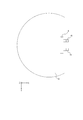
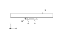
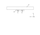
- (Second modified example) 7A to 7C are diagrams showing the wiring board 12 and the like in the electronic device according to the second modification.
- the electronic device according to the second modification differences from the electronic device 1 described with reference to FIGS. 1 to 5 will be mainly described.
- FIGS. 7A to 7C the components such as the load circuit 13 shown in FIGS. 1 and 2 are omitted, and only the wiring substrate 12, the terminal 15 and the support plate 18 are shown and described.
- the electronic device according to the second modification is different from the electronic device 1 described with reference to FIGS. 1 to 5 and the like in that the support plate 18 is further arranged on the wiring board 12.
- FIG. 7A is a diagram of the wiring board 12, the terminal 15, and the support plate 18 in the electronic device according to the second modification as viewed from the Z-axis negative direction side.
- FIG. 7B is a diagram of the wiring board 12, the terminal 15, and the support plate 18 in the electronic device according to the second modification as viewed from the X-axis positive direction side.
- FIG. 7C is a diagram of the wiring board 12, the terminal 15, and the support plate 18 in the electronic device according to the second modification as viewed from the X-axis negative direction side.
- the support plate 18 is arranged on the same surface of the wiring board 12 as the surface on which the terminals 15 are arranged. That is, the support plate 18 is arranged on the surface of the wiring substrate 12 on the Z axis negative direction side. As shown in FIGS. 7A to 7C, the support plate 18 is located on the X axis negative direction side with respect to the terminal 15. That is, the support plate 18 is located on the side opposite to the second housing 20 with respect to the terminal 15.
- the support plate 18 is in contact with a part of the surface of the terminal 15 on the X axis negative direction side, and restricts the deformation of the terminal 15 to the X axis negative direction side.
- the support plate 18 may be made of, for example, a resin or a metal whose surface is insulation-coated.
- the terminal 15 may be deformed in the negative direction of the X-axis, which may cause poor contact between the terminal 15 and the connector 32 of the energy harvesting module 30.
- the support plate 18 is positioned on the X-axis negative direction side of the wiring board 12 with respect to the terminal 15 as described above, the deformation of the terminal 15 to the X-axis negative direction side can be restricted. .. As a result, it is possible to reduce the risk of poor contact between the terminal 15 and the connector 32 of the energy harvesting module 30.
- an electronic device capable of easily mechanically and electrically connecting the energy harvesting module and the wiring board.
Landscapes
- Engineering & Computer Science (AREA)
- Microelectronics & Electronic Packaging (AREA)
- Details Of Connecting Devices For Male And Female Coupling (AREA)
- Connector Housings Or Holding Contact Members (AREA)
- Coupling Device And Connection With Printed Circuit (AREA)
- Charge And Discharge Circuits For Batteries Or The Like (AREA)
- Battery Mounting, Suspending (AREA)
Priority Applications (1)
| Application Number | Priority Date | Filing Date | Title |
|---|---|---|---|
| JP2020553772A JP7338635B2 (ja) | 2018-10-31 | 2019-10-17 | 電子機器 |
Applications Claiming Priority (2)
| Application Number | Priority Date | Filing Date | Title |
|---|---|---|---|
| JP2018-205718 | 2018-10-31 | ||
| JP2018205718 | 2018-10-31 |
Publications (1)
| Publication Number | Publication Date |
|---|---|
| WO2020090496A1 true WO2020090496A1 (ja) | 2020-05-07 |
Family
ID=70464454
Family Applications (1)
| Application Number | Title | Priority Date | Filing Date |
|---|---|---|---|
| PCT/JP2019/040869 Ceased WO2020090496A1 (ja) | 2018-10-31 | 2019-10-17 | 電子機器 |
Country Status (3)
| Country | Link |
|---|---|
| JP (1) | JP7338635B2 (cg-RX-API-DMAC7.html) |
| TW (1) | TW202029519A (cg-RX-API-DMAC7.html) |
| WO (1) | WO2020090496A1 (cg-RX-API-DMAC7.html) |
Citations (6)
| Publication number | Priority date | Publication date | Assignee | Title |
|---|---|---|---|---|
| JP2002329416A (ja) * | 2001-04-27 | 2002-11-15 | Sanyo Electric Co Ltd | 人体センサーを有する電子機器 |
| JP2003132989A (ja) * | 2001-10-26 | 2003-05-09 | Hosiden Corp | コネクタ |
| US20080092941A1 (en) * | 2006-10-24 | 2008-04-24 | Hon Hai Precision Industry Co., Ltd. | Portable computer with detachable solar cell module |
| JP2009266411A (ja) * | 2008-04-22 | 2009-11-12 | Nec Saitama Ltd | ジャックコネクタ及びこれを備えた携帯端末 |
| US20100202627A1 (en) * | 2009-01-15 | 2010-08-12 | Randolph Gray | Docking System Employing a Solar Energy Charging System |
| JP2014010527A (ja) * | 2012-06-28 | 2014-01-20 | Koha Co Ltd | 自動販売機 |
-
2019
- 2019-10-17 WO PCT/JP2019/040869 patent/WO2020090496A1/ja not_active Ceased
- 2019-10-17 JP JP2020553772A patent/JP7338635B2/ja active Active
- 2019-10-23 TW TW108138267A patent/TW202029519A/zh unknown
Patent Citations (6)
| Publication number | Priority date | Publication date | Assignee | Title |
|---|---|---|---|---|
| JP2002329416A (ja) * | 2001-04-27 | 2002-11-15 | Sanyo Electric Co Ltd | 人体センサーを有する電子機器 |
| JP2003132989A (ja) * | 2001-10-26 | 2003-05-09 | Hosiden Corp | コネクタ |
| US20080092941A1 (en) * | 2006-10-24 | 2008-04-24 | Hon Hai Precision Industry Co., Ltd. | Portable computer with detachable solar cell module |
| JP2009266411A (ja) * | 2008-04-22 | 2009-11-12 | Nec Saitama Ltd | ジャックコネクタ及びこれを備えた携帯端末 |
| US20100202627A1 (en) * | 2009-01-15 | 2010-08-12 | Randolph Gray | Docking System Employing a Solar Energy Charging System |
| JP2014010527A (ja) * | 2012-06-28 | 2014-01-20 | Koha Co Ltd | 自動販売機 |
Also Published As
| Publication number | Publication date |
|---|---|
| JPWO2020090496A1 (ja) | 2021-09-24 |
| TW202029519A (zh) | 2020-08-01 |
| JP7338635B2 (ja) | 2023-09-05 |
Similar Documents
| Publication | Publication Date | Title |
|---|---|---|
| TWI431877B (zh) | 接線盒及其導線連接裝置 | |
| US7655859B2 (en) | Connector for a solar module | |
| CN101103466A (zh) | 用于太阳能电池板的接线箱以及带有接线箱的太阳能电池板 | |
| US20230308028A1 (en) | Dc-ac converter, and ac output device | |
| JP7012258B2 (ja) | 照明装置及び照明器具 | |
| JP2010097723A (ja) | 電池パック | |
| JP7182143B2 (ja) | 蓄電池ユニットおよびシステム | |
| US6364696B1 (en) | Battery carrying portable electric equipment | |
| JP2018137104A (ja) | 電池ユニット及び照明器具 | |
| JP5555085B2 (ja) | 太陽電池モジュール | |
| JP7338635B2 (ja) | 電子機器 | |
| CN208113073U (zh) | 电子电路单元及电气设备 | |
| JP2018137182A (ja) | 照明器具 | |
| KR100579897B1 (ko) | 태양광모듈용 프레임 와이어링 구조 및 조립방법 | |
| JP2018147586A (ja) | 電池ユニット及び照明器具 | |
| KR20160028750A (ko) | 배터리 팩 | |
| CN222463046U (zh) | 便携式储能装置 | |
| CN211405507U (zh) | 一种太阳能充电控制器 | |
| EP4645683A1 (en) | Microinverter | |
| JP2023046029A (ja) | 蓄電モジュール | |
| JP2011018674A (ja) | 太陽電池モジュール用端子ボックス | |
| JP6857844B2 (ja) | 非常用照明装置及び照明器具 | |
| JP6870458B2 (ja) | 電力変換装置 | |
| JP2018147588A (ja) | 照明器具 | |
| TW202007914A (zh) | 電子設備 |
Legal Events
| Date | Code | Title | Description |
|---|---|---|---|
| 121 | Ep: the epo has been informed by wipo that ep was designated in this application |
Ref document number: 19878987 Country of ref document: EP Kind code of ref document: A1 |
|
| ENP | Entry into the national phase |
Ref document number: 2020553772 Country of ref document: JP Kind code of ref document: A |
|
| NENP | Non-entry into the national phase |
Ref country code: DE |
|
| 122 | Ep: pct application non-entry in european phase |
Ref document number: 19878987 Country of ref document: EP Kind code of ref document: A1 |