WO2020085037A1 - 描画方法および描画装置 - Google Patents
描画方法および描画装置 Download PDFInfo
- Publication number
- WO2020085037A1 WO2020085037A1 PCT/JP2019/039234 JP2019039234W WO2020085037A1 WO 2020085037 A1 WO2020085037 A1 WO 2020085037A1 JP 2019039234 W JP2019039234 W JP 2019039234W WO 2020085037 A1 WO2020085037 A1 WO 2020085037A1
- Authority
- WO
- WIPO (PCT)
- Prior art keywords
- substrate
- light beam
- range
- follow
- incident
- Prior art date
- Legal status (The legal status is an assumption and is not a legal conclusion. Google has not performed a legal analysis and makes no representation as to the accuracy of the status listed.)
- Ceased
Links
Images









Classifications
-
- G—PHYSICS
- G03—PHOTOGRAPHY; CINEMATOGRAPHY; ANALOGOUS TECHNIQUES USING WAVES OTHER THAN OPTICAL WAVES; ELECTROGRAPHY; HOLOGRAPHY
- G03F—PHOTOMECHANICAL PRODUCTION OF TEXTURED OR PATTERNED SURFACES, e.g. FOR PRINTING, FOR PROCESSING OF SEMICONDUCTOR DEVICES; MATERIALS THEREFOR; ORIGINALS THEREFOR; APPARATUS SPECIALLY ADAPTED THEREFOR
- G03F7/00—Photomechanical, e.g. photolithographic, production of textured or patterned surfaces, e.g. printing surfaces; Materials therefor, e.g. comprising photoresists; Apparatus specially adapted therefor
- G03F7/20—Exposure; Apparatus therefor
Definitions
- the present invention relates to control of a drawing device that irradiates a substrate with a convergent light beam to perform drawing, and particularly relates to control of a convergent position of the light beam.
- a substrate on which a photosensitive layer is formed is used as a drawing object, and the drawing object is irradiated with light modulated based on drawing data to expose the photosensitive layer.
- a spatial light modulator can be preferably applied as an optical modulator for performing such light modulation. For example, in the drawing device disclosed in Patent Document 1 previously disclosed by the applicant of the present application, line beam light is made incident on the spatial light modulator.
- the reflected light modulated is converged by the optical system, and is incident as a converged light beam on the substrate which is the object to be drawn to perform drawing. ing.
- an autofocus mechanism that always converges the light beam at the substrate surface position is provided. It is equipped.
- the autofocus mechanism detects the substrate surface position from the light receiving position of the reflected light of the light incident on the substrate surface, and moves the focusing lens up and down according to the detection result.
- the substrates to be processed may include those having a height difference on the surface.
- a substrate arranged by attaching semiconductor chips to be drawn on the surface of a flat base material.
- the present invention has been made in view of the above problems, and in a technique of irradiating a substrate with a converged light beam to perform drawing, there is provided a technique capable of appropriately causing the light beam to follow the surface of a substrate having a height difference on the surface.
- the purpose is to provide.
- a stage on which a substrate having a height difference on a surface is placed in a horizontal posture, and a drawing head for irradiating a surface of the substrate with a converged light beam to draw a pattern are relatively moved.
- a step of optically detecting a surface position of the substrate on which the light beam is incident Adjusting the converging position of the light beam in the optical axis direction to follow the surface of the substrate based on the detection result of the surface position, and adjusting the converging position is performed relative to the periphery of the surface of the substrate. Is restricted within a follow-up range set based on the detection result of the surface position of the substrate in each of the protruding region that protrudes and the retracted region that relatively retracts from the protruding region.
- one aspect of the drawing apparatus irradiates a stage on which a substrate having a height difference on the surface can be placed in a horizontal posture, and irradiates a converged light beam on the surface of the substrate.
- a focus adjusting unit for adjusting the convergent position of the light beam in the optical axis direction within a predetermined following range to follow the surface of the substrate based on the detection result of the detecting unit.
- the follow-up range is a detection result of the surface position of the substrate in each of a projecting region relatively projecting from the periphery of the surface of the substrate and a receding region relatively receding from the projecting region. It is previously set based on.
- the following range of the light beam convergence position with respect to the substrate surface in the optical axis direction is regulated.
- the follow-up range is set based on the detection result of the surface position in each of the projecting region that projects relatively to the periphery of the substrate surface and the receding region around the projecting region. Therefore, for example, it is possible to control so that the light beam follows the surface of the substrate as a whole in the protruding region, but does not follow the receding region. That is, it is possible to regulate the follow-up to the substrate surface in an unnecessary area.
- By setting the follow-up range based on the actual detection result rather than simply setting the uniform follow-up range, it is possible to perform accurate control according to the surface state of the substrate.
- the convergent position of the light beam is set within the following range set based on the detection result of the protruding region and the receding region. It is controlled so as to follow the surface of the substrate. Therefore, the light beam can be appropriately made to follow the surface of the substrate having a height difference on the surface.
- FIG. 1 is a front view schematically showing a schematic configuration of a drawing device according to the present invention.
- XYZ orthogonal coordinates are set as shown in FIG.
- the XY plane is the horizontal plane
- the Z direction is the vertical direction. More specifically, the ( ⁇ Z) direction represents the vertically downward direction.
- the drawing device 100 is a device that draws a pattern by irradiating light onto the upper surface of the substrate W on which a layer of a photosensitive material such as a resist is formed.
- a photosensitive material such as a resist
- As the substrate W various substrates such as a semiconductor substrate, a printed circuit board, a color filter substrate, a glass substrate for a flat panel display provided in a liquid crystal display device or a plasma display device, a substrate for an optical disk, and the like can be applied.
- the drawing apparatus 100 includes an inside of a main body formed by attaching a cover panel (not shown) to a ceiling surface and a peripheral surface of a skeleton composed of the main body frame 101, and an outside of the main body that is an outside of the main body frame 101. It has a configuration in which various components are arranged.
- the inside of the main body of the drawing apparatus 100 is divided into a processing area 102 and a transfer area 103.
- the processing area 102 among these areas the stage 10, the stage moving mechanism 20, the optical unit U, and the alignment unit 60 are mainly arranged.
- a transfer device 70 such as a transfer robot that transfers the substrate W in and out of the processing area 102 is arranged.
- An illumination unit 61 that supplies illumination light to the alignment unit 60 is arranged outside the main body of the drawing apparatus 100.
- a control unit 90 that is electrically connected to each unit of the drawing apparatus 100 and controls the operation of each unit is disposed in the main body.
- a cassette mounting unit 104 for mounting the cassette C is arranged outside the main body of the drawing apparatus 100 and adjacent to the transfer area 103.
- the transport device 70 which corresponds to the cassette placing section 104 and is arranged in the transfer area 103 inside the main body, takes out the unprocessed substrate W accommodated in the cassette C placed on the cassette placing section 104 and processes it.
- the substrate W that has been processed is carried in (loaded), and the processed substrate W is carried out (unloaded) from the processing area 102 and accommodated in the cassette C.
- the delivery of the cassette C to and from the cassette placement unit 104 is performed by an external transport device (not shown).
- the loading process of the unprocessed substrate W and the unloading process of the processed substrate W are performed by operating the transfer device 70 in accordance with an instruction from the control unit 90.
- the stage 10 has a flat plate-shaped outer shape, and is a holding unit that holds and holds the substrate W in a horizontal posture on its upper surface.
- a plurality of suction holes are formed on the upper surface of the stage 10.
- a negative pressure suction pressure
- the substrate W placed on the stage 10 can be fixedly held on the upper surface of the stage 10.
- the stage 10 is moved by the stage moving mechanism 20.
- the stage moving mechanism 20 is a mechanism that moves the stage 10 in the main scanning direction (Y axis direction), the sub scanning direction (X axis direction), and the rotation direction (rotation direction around the Z axis).
- the stage moving mechanism 20 includes a base plate 24 that supports a support plate 22 that rotatably supports the stage 10, a sub-scanning mechanism 23 that moves the support plate 22 in the sub-scanning direction, and a main scanning unit that moves the base plate 24 in the main-scanning direction. And a scanning mechanism 25.
- the sub-scanning mechanism 23 and the main scanning mechanism 25 move the stage 10 in response to an instruction from the control unit 90.
- Alignment unit 60 images an alignment mark (not shown) formed on the upper surface of substrate W.
- the alignment unit 60 includes an alignment camera 601 having a lens barrel, an objective lens, and a CCD image sensor.
- the CCD image sensor included in the alignment camera 601 is composed of, for example, an area image sensor (two-dimensional image sensor). Further, the alignment unit 60 is supported by a lifting mechanism (not shown) so as to be lifted and lowered within a predetermined range.
- the illumination unit 61 is connected to the lens barrel via a fiber 611 and supplies illumination light to the alignment unit 60.
- the light guided by the fiber 611 extending from the illumination unit 61 is guided to the upper surface of the substrate W via the lens barrel of the alignment camera 601, and the reflected light is received by the CCD image sensor via the objective lens.
- the upper surface of the substrate W is imaged and imaging data is acquired.
- the alignment camera 601 is electrically connected to the image processing unit of the control unit 90, acquires imaging data according to an instruction from the control unit 90, and transmits the acquired imaging data to the control unit 90.
- control unit 90 Based on the imaging data provided from the alignment camera 601, the control unit 90 detects the reference mark provided at the reference position of the substrate W and performs the alignment process of positioning the relative position between the optical unit U and the substrate W. Then, pattern drawing is performed by irradiating a predetermined position on the substrate W with laser light modulated according to the drawing pattern from the optical unit U.
- the optical unit U has a schematic configuration in which two optical heads 4 that modulate laser light based on strip data corresponding to a drawing pattern are arranged along the X-axis direction.
- the number of optical heads 4 is not limited to this. Since these optical heads 4 have the same configuration, the configuration related to one optical head 4 will be described below.
- the optical unit U is provided with a light irradiation unit 5 that irradiates the optical head 4 with laser light.
- the light irradiation unit 5 has a laser drive unit 51, a laser oscillator 52, and an illumination optical system 53. Then, the laser light emitted from the laser oscillator 52 by the operation of the laser drive unit 51 is applied to the optical head 4 via the illumination optical system 53.
- the optical head 4 modulates the laser light emitted from the light emitting unit 5 by the spatial light modulator, and makes the substrate W moving immediately below the optical head 4 fall onto the substrate W. As a result, the unprocessed substrate W is drawn by exposure.
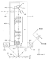
- FIG. 2 is a diagram schematically showing an example of a detailed configuration of the optical head.
- the optical head 4 is provided with a spatial light modulator 41 having a diffractive optical element 410.
- the spatial light modulator 41 attached to the upper part of the support column 400 extending in the vertical direction (Z direction) on the optical head 4 has the reflecting surface of the diffractive optical element 410 facing downward,
- the support 400 is supported by the movable stage 414.
- the diffractive optical element 410 is arranged such that the normal line of its reflection surface is inclined with respect to the optical axis OA, and the light emitted from the illumination optical system 53 passes through the opening of the support column 400 and the mirror 42. Is incident on the diffractive optical element 410 and reflected by the mirror 42. Then, the state of each channel of the diffractive optical element 410 is switched by the control unit 90 according to the drawing data, and the laser light incident on the diffractive optical element 410 is modulated.
- the laser beam light reflected from the diffractive optical element 410 as the 0th-order diffracted light enters the lens of the projection optical system 43, while the laser beam reflected from the diffractive optical element 410 as the 1st-order or higher-order diffracted light is projected onto the projection optical system. It does not enter the lens 43. That is, basically, only the 0th-order diffracted light reflected by the diffractive optical element 410 is configured to enter the projection optical system 43.
- the light that has passed through the lens of the projection optical system 43 is converged by the focusing lens 441 and guided onto the substrate W as a converged light beam at a predetermined magnification.
- the focusing lens 441 is attached to the focus drive mechanism 442. Then, the focus driving mechanism 442 moves the focusing lens 441 up and down along the vertical direction (Z-axis direction) in response to a control command from the control unit 90, so that the convergence position of the beam light emitted from the focusing lens 441 is set to the substrate.
- the upper surface Ws of W is adjusted.
- the irradiation unit 451 causes the light emitted from the light source configured by the laser diode (LD) to be obliquely incident on the upper surface Ws of the substrate W.
- the light receiving unit 452 is configured by a solid-state image sensor such as a CMOS (Complementary Metal Oxide Semiconductor) sensor or a CCD (Charge Coupled Device) sensor, and detects reflected light from the upper surface Ws of the substrate W. Then, the control unit 90 detects the position of the substrate upper surface Ws in the Z direction, that is, the distance between the optical head 4 and the substrate upper surface Ws, from the detection result of the light receiving unit 452.
- CMOS Complementary Metal Oxide Semiconductor
- CCD Charge Coupled Device
- the controller 90 uses this to detect the distance between the optical head 4 and the substrate upper surface Ws.
- control unit 90 operates the focus driving mechanism 442 according to the detected distance to move the focusing lens 441 up and down. In this way, the focus of the focusing lens 441 is adjusted to the upper surface Ws of the substrate, and the focus position of the laser light is accurately adjusted to the upper surface Ws of the substrate (autofocus).
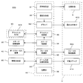
- FIG. 3 is a block diagram showing the control system of this drawing device.
- a CPU (not shown) executes a control program stored in the storage unit 99 in advance, or dedicated hardware implements the following functional blocks 91 to 96.
- the illumination control unit 91 controls the light irradiation unit 5 of the optical unit U to emit the beam light.
- the drawing control unit 92 controls the driver 921 based on the drawing recipe stored in the storage unit 99, applies a control voltage from the driver 921 to the diffractive optical element 410, and modulates the beam light corresponding to the pattern to be drawn. To do.
- the focus control unit 95 controls the autofocus operation. Specifically, the focus control unit 95 detects the position of the substrate upper surface Ws based on the output from the light receiving unit 452 of the autofocus mechanism 45, and from the result, adjusts the focus FP of the converged light beam to the substrate upper surface Ws. The focus adjustment amount required for the calculation is transmitted to the focus drive mechanism 442.
- the stage controller 94 controls the stage moving mechanism 20 to move the stage 10 relative to the optical head 4.
- the alignment control unit 93 executes the alignment process based on the image data output from the alignment camera 601 of the alignment unit 60.
- the beam incident position control unit 96 executes an incident position adjusting process for optimizing the position of the line beam light incident on the diffractive optical element 410, if necessary.
- the movable stage 414 of the spatial light modulator 41 is operated based on the output signal from the observation optical system 80 which is provided on the side of the stage 10 and measures the incident direction of the light beam from the optical head 4. Note that, for specific methods such as incident position adjustment processing, autofocus adjustment, alignment adjustment, etc., for example, the method described in Patent Document 1 can be applied.
- the drawing apparatus 100 can perform drawing by exposure on various substrates.
- a drawing operation when drawing is performed on a semiconductor substrate in which a plurality of semiconductor device regions are arranged in a two-dimensional matrix on a substantially rectangular substrate will be described.
- This drawing operation is realized by the control unit 90 executing a control program prepared in advance and causing each unit of the apparatus to perform a predetermined operation.
- FIG. 4 is a flowchart showing the drawing operation by this drawing device.
- a drawing recipe representing the contents to be drawn is acquired (step S101), and the unprocessed substrate W, which is an object to be drawn, is carried into the stage 10 from the cassette C (step S102).
- the drawing recipe is stored and stored in the storage unit 99.
- the alignment unit 60 performs alignment processing for aligning the relative positions of the substrate W and the optical head 4 (step S103). Thereby, the pattern drawing position on the substrate W is precisely adjusted.
- the drawing controller 92 prepares drawing data based on the drawing recipe (step S104), and supplies the drawing data to the spatial light modulator 41 of the optical head 4 to irradiate the substrate W while modulating the light beam.
- Drawing processing is performed (step S105).
- the processed substrate W is unloaded from the stage 10 and accommodated in the cassette C (step S106).
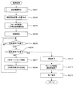
- FIG. 5 is a flowchart showing the drawing process.
- the "following range setting process” is executed (step S201), which will be described later in detail.
- the substrate W and the optical head 4 are relatively positioned at a predetermined drawing start position (step S202), focus control by the autofocus mechanism 45 and scanning movement of the substrate W in the Y direction by the stage moving mechanism 20. Is started (step S203).
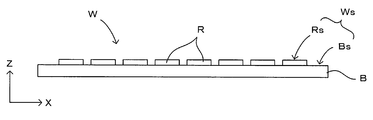
- FIG. 6A to 6C are diagrams showing an example of a substrate which is a target of a drawing process.
- FIG. 6A is a plan view of a substrate W as an object to be processed.
- 6B is a sectional view taken along the line AA of FIG. 6A, which will be described later.
- FIG. 6C is a diagram showing an example of the path of the scanning movement of the light beam with respect to the substrate W.
- the substrate has a rectangular outer shape here, the drawing process is not limited to this, and the drawing process can be performed on a circular substrate, for example.
- the substrate W is, for example, a glass substrate, a ceramic plate, a semiconductor wafer, or another substantially rectangular base material B, on the surface of which a device region R composed of a plurality of semiconductor chips or the like to be drawn is arranged in a two-dimensional matrix.
- the drawing apparatus 100 draws a predetermined drawing pattern on each device region R as a part of a manufacturing process for manufacturing a semiconductor device on each device region R.
- the patterns drawn in the respective device areas R are the same, so the drawing apparatus 100 sequentially draws the drawing patterns in accordance with the drawing data given in advance in the respective device areas R.
- the drawing position of the substrate upper surface Ws by the optical head 4 is sequentially changed by horizontally moving the substrate W mounted on the stage 10 and the optical head 4 relatively, that is, by scanning.
- FIG. 6C is a diagram showing an example of a path of scanning movement.
- the scanning movement is realized by moving the stage 10 on which the substrate W is placed in the XY directions.
- the drawing position is first moved in the (+ Y) direction with the position corresponding to the lower left of the substrate W in the drawing as the drawing start position Ps.
- the drawing position advances to the upper left end of the substrate W, the drawing position moves in the (+ X) direction by a predetermined pitch Px.
- the moving direction is then reversed to the (-Y) direction.
- the drawing position reaches the lower end of the substrate W in the figure, that is, the end on the ( ⁇ Y) side, the drawing position is moved again in the (+ X) direction by a predetermined pitch Px and again moved in the (+ X) direction.
- the relative movement between the substrate W and the optical head 4 is a combination of the scanning movement in the (+ Y) direction or the ( ⁇ Y) direction and the pitch feed movement in the (+ X) direction alternately. ing.
- the drawing position reaches the position corresponding to the lower right of the substrate W, the scanning movement ends.
- main scanning movement the movement of the drawing position in the Y direction
- Y direction is referred to as “main scanning direction”.
- the pitch feed of the drawing position in the X direction is referred to as "sub scanning movement”
- the X direction is referred to as "sub scanning direction”.
- Drawing is started by emitting a modulated light beam according to drawing data from the optical head 4 (step S204). That is, while the focus control and the main scanning movement in the (+ Y) direction are performed, the optical head 4 irradiates the substrate W with light, thereby writing on the substrate upper surface Ws.
- the drawing position reaches the main scanning end position in the Y direction in the first main scanning movement (step S205)
- the drawing position is moved by one step in the X direction, more specifically, by the feed pitch Px in the (+ X) direction.
- the main scanning movement direction is reversed to the (-Y) direction (step S208).
- the second main scanning movement is started.
- drawing is completed for all the device regions R of the substrate W.
- step S211 the emission of the light beam from the optical head 4 is finished (step S211), and the focus control and the scanning movement are finished (step S212). Then, an ending operation for shifting each part of the apparatus to a predetermined ending state is executed (step S213), and the drawing process for one substrate W ends.
- the plurality of device regions R are arranged in a two-dimensional matrix on the surface Bs of the base material B at regular intervals in the X and Y directions. Therefore, as shown in FIG. 6B, a height difference corresponding to the thickness of the semiconductor chip forming the device region R exists between the surface (upper surface) Bs of the base material B and the upper surface Rs of the device region R. . Further, there is a gap between the adjacent device regions R, and the base material surface Bs is exposed from this gap. For this reason, when the base material B and the device region R are regarded as an integrated substrate W, a periodic step exists on the substrate upper surface Ws.
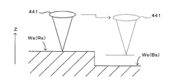
- FIG. 7A and 7B are diagrams showing the relationship between the step of the substrate and the autofocus control.
- the focusing lens 441 is moved up and down according to the height of the substrate upper surface Ws so that the light beam always converges on the substrate upper surface Ws. Therefore, if the tracking range is not limited, as shown in FIG. 7A, the focusing lens 441 moves up and down so that the substrate W having a step moves in parallel along the step.
- the drawing target is the upper surface Rs of the device region R protruding from the periphery of the substrate upper surface Ws, and it is not necessary to focus on the base material upper surface Bs recessed from this. Rather, mechanical troubles caused by the focusing lens 441 moving excessively, or a temporary defocus state on the device region upper surface Rs due to a response delay when the object to be tracked moves from the substrate upper surface Bs to the device region upper surface Rs, etc. However, many harmful effects can occur.
- the convergent position of the light beam always correctly follows the device region upper surface Rs, but does not follow the base material upper surface Bs at a predetermined position. Focus control that stays at is desirable. Details of focus control for enabling this will be described below.
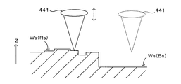
- FIG. 8A and 8B are diagrams showing the concept of focus control in this embodiment. As shown in FIG. 8A, in focus control for the purpose of drawing in the device region R, it is necessary to reliably follow small irregularities that may exist on the upper surface Rs of the device region that is the target of drawing. On the other hand, it is not necessary to make the focus follow the upper surface Bs of the base material that is not the drawing target.
- the follow-up range Rt including the upper surface Rs of the device region R in the Z direction and having a certain spread is set on the upper side and the lower side thereof.
- the convergent position of the light beam is surely made to follow the upper surface Ws of the substrate detected within the following range Rt.
- the beam converging position is not moved outside the follow-up range Rt, but an appropriate position within the follow-up range Rt (following example).
- the lower limit of the range Rt) should be kept.
- the vertical movement of the focusing lens 441 associated with the focus control is limited to the spread width of the follow-up range Rt, and a large movement that follows the base material upper surface Bs that does not require drawing is suppressed. Further, when the upper surface Rs of the device region is again detected within the tracking range Rt and the tracking is restarted, the focusing lens 441 is located at a relatively close position, so that the tracking can be restarted promptly.
- the follow-up range Rt must surely include the upper surface Rs of the device region R and does not include the base material upper surface Bs other than the device region R. Considering the individual variation of each part of the drawing apparatus 100 and the substrate W, it is impossible to set the follow-up range Rt uniformly in advance.
- the follow-up range Rt needs to be dynamically set for each combination of the drawing apparatus 100 and the substrate W.
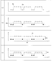
- FIG. 9 is a diagram showing the principle of the method of setting the tracking range.
- a threshold value Zth is set between them as shown in the column (b) of FIG.
- Sampling data larger than the threshold value (white circle) can be treated as corresponding to the device region upper surface Rs
- small sampling data black circle
- a curve Cr representing each surface profile is obtained.
- Cb can be obtained.
- the distance ⁇ Z between the curves Cr and Cb in the Z direction represents the height difference between the device region upper surface Rs and the base material upper surface Bs.
- the tracking range Rt can be determined by utilizing this height difference. For example, about 50% to 150% of the height difference ⁇ Z can be set as the width of the follow-up range Rt.
- the follow-up range Rt In order to ensure the follow-up on the device area upper surface Rs, it is desirable that the follow-up range Rt completely includes the approximated curve Cr corresponding to the device area upper surface Rs. Therefore, the follow-up range Rt is not constant in the Y direction, and when there is a height variation of the device region upper surface Rs, it has position dependency in conjunction with this.
- a curve obtained by offsetting the approximated curve Cr in the upward direction and the downward direction by a predetermined value can be used as the curves representing the upper limit and the lower limit of the following range Rt.
- the offset amount does not necessarily have to be the same in the upward and downward directions of the approximate curve Cr.
- the offset amount in the downward direction cannot be made too large in order to avoid erroneous determination that the base material upper surface Bs is the device area upper surface Rs.
- the amount of offset in the upward direction may be made larger than that in the downward direction while maintaining the width of the tracking range Rt.
- FIG. 10 is a diagram showing a method of setting the follow-up range when the substrate has a small warp.
- a waviness due to the warp appears in the sampling data distribution.
- columns (b) to (d) of FIG. 10 if the waviness is relatively small and there is no influence on the separation between the data corresponding to the device region upper surface Rs and the data corresponding to the base material upper surface Bs, The follow-up range Rt can be determined in the same way.
- the curves representing the upper limit and the lower limit of the follow-up range Rt also have undulations due to the warp of the substrate W.
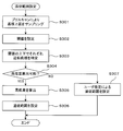
- FIG. 11 is a flowchart showing the processing for setting the tracking range. This process is a process for setting the follow-up range Rt according to the above principle, and is carried out after the substrate W is loaded into the drawing apparatus 100 and before the drawing process is executed (step S201 in FIG. 5).
- the substrate W is pre-scanned (step S301).
- the pre-scan is an operation of scanning and moving the optical head 4 with respect to the substrate W without irradiating light for drawing, and sampling is performed at the position of the upper surface Ws of the substrate according to the above principle.
- a sampling data string as shown in the column (a) of FIG. 9 or the column (a) of FIG. 10 is acquired.
- the scanning of the optical head 4 for the prescan may be performed for one row in the Y direction from the drawing start position Ps shown in FIG. 6C.
- an appropriate threshold value Zth is set for the obtained sampling data string (step S302), and the approximate curves Cr and Cb are set for the data larger and smaller than the threshold value Zth, respectively. It is specified (step S303).
- the sampling data string corresponds to the data corresponding to the device region upper surface Rs and the base material upper surface Bs in a simple threshold setting. It may not be possible to divide it into two parts. In such a case, the obtained approximate curves Cr and Cb are not sufficiently separated from each other, and a significant difference in height ⁇ Z cannot be obtained. In such a case, it is considered impossible to calculate the height difference (NO in step S304), and the follow-up range Rt is left to the user setting (step S307).
- step S304 When the approximate curves Cr and Cb are well separated and a significant height difference ⁇ Z is obtained (YES in step S304), the value ⁇ Z is obtained (step S305), and the follow-up range Rt is further set (step S306). These processes are in accordance with the principle described above. In this way, the follow-up range Rt is set.
- FIG. 12 is a flowchart showing focus control processing. This process is periodically executed each time a predetermined adjustment timing comes while the drawing apparatus 100 executes the drawing process.
- the adjustment timing comes (step S401)
- the current Z-direction position of the substrate upper surface Ws is acquired based on the light reception result from the light receiving section 452 of the autofocus mechanism 45 (step S402).
- the tracking range Rt is updated as needed (step S403), which will be described later.
- the light beam convergence position is adjusted to the position based on the acquired substrate upper surface position detection result.
- the amount of focus adjustment required for is calculated (step S405).
- step S4 when the acquired substrate upper surface position is not within the follow-up range Rt (NO in step S404), it is determined whether it is outside the upper limit side or outside the lower limit side (step S411).
- the upper limit value of the tracking range Rt is set as a target for beam position control (step S412), and when it is out of the lower limit side (NO in step S411).
- the lower limit of the tracking range Rt is set as a target for beam position control (step S413). Then, the focus adjustment amount required to match the convergent position of the light beam to the set target position is obtained (step S405).
- step S405 When an adjustment amount for adjusting the beam position to a desired position is obtained (step S405), a control command including the obtained focus adjustment amount is given from the focus control unit 95 of the control unit 90 to the focus drive mechanism 442. Focus adjustment is performed by adjusting the Z-direction position Zf of the focusing lens 441 accordingly (step S406).
- the focusing lens 441 is not driven beyond the tracking range Rt. That is, in such a case, the beam convergence position is controlled with the upper limit or the lower limit of the tracking range Rt as the target.
- FIG. 13A and 13B are diagrams showing the outline of the update processing of the follow range.
- the amount of information representing the upper surface position variation of the substrate W in the X direction increases.
- the follow-up range Rt initially set may not be appropriate from the current position of the upper surface Ws of the substrate.
- One of the methods for avoiding this problem is to shift the follow-up range Rt in the Z direction corresponding to the variation of the upper surface position of the substrate W in the X direction.
- FIG. 13B the follow-up range Rt1 applied during the first main-scan movement is gradually shifted to Rt2, Rt3, ... In response to the change in the upper surface position of the substrate W during the subsequent main-scan movement. Is shown to be done.
- the follow-up range Rt5 in the fifth main-scan movement the follow-up range Rt4 in the fourth main-scan movement shifted in the Z direction by (Z4-Z3) can be applied. In this way, it is possible to derive an updated follow-up range applicable to the subsequent main-scan movement from the change range of the follow-up range and the substrate upper surface position applied in the past main-scan movement.
- the follow-up range Rt in which the variation in the Y direction is taken into consideration is set based on the position detection result of the device region upper surface Rs and the base material upper surface Bs obtained by the prescan in the Y direction. .
- This is applied to the focus control while being corrected and updated according to the track record of the fluctuation in the X direction. Therefore, even in the substrate W having a step between the device region upper surface Rs and the base material upper surface Bs, the light beam is converged on the device area upper surface Rs that is a drawing target and avoids following the base material upper surface Bs that is not a drawing target. can do.
- the substrate W corresponds to the “substrate” of the present invention
- the substrate upper surface Ws corresponds to the “substrate surface” of the present invention
- the stage 10 functions as the “stage” of the present invention.
- the optical head 4 functions as the “drawing head” of the present invention
- the stage moving mechanism 20 functions as the “scanning moving section” of the present invention.
- the autofocus mechanism 45 functions as the “detection unit” of the invention
- the focus drive mechanism 442 functions as the “focus adjustment unit” of the invention.
- the upper surface Rs of the device area in the substrate upper surface Ws corresponds to the “protruding area” of the present invention
- the base material upper surface Bs corresponds to the “receding area” of the present invention
- the present invention is not limited to the above-described embodiment, and various modifications other than those described above can be made without departing from the spirit of the present invention.
- the above embodiment is a drawing apparatus that uses the diffractive optical element 410 as a light beam modulating unit, but the modulation method is not limited to this, and the present invention is applied to an apparatus that performs drawing by an arbitrary modulation method. It is possible to
- the convergent position of the light beam is set to the upper limit value or the lower limit value of the tracking range. It may be set at any position inside.
- drawing is performed on the device area Rs, which is a “projection area” that protrudes from the surroundings on the upper surface Ws of the substrate, and the follow-up range is set so as to include the height of the device area Rs. .
- the setting of the follow-up range includes the height of the retracted area that is the drawing target, but does not include the height of the protruding area that is not the drawing target. It should be done. As a result, the light beam surely converges following the surface of the receding area that is the drawing target, but does not follow the protruding area, so avoiding unnecessary convergence operation as in the above embodiment. Is possible.
- the “detection unit” of the present invention is not limited to such a principle, and various mechanisms for acquiring the position of the substrate surface by an optical method can be used.
- the substrate W used in the above-described embodiment is a substrate B to which a semiconductor chip as the device region R is attached.
- the present invention works effectively.
- the application target of the present invention is not limited to an apparatus that irradiates light on a semiconductor substrate W such as a wafer as an object to be drawn and draws the same, and various objects such as a printed wiring board and a glass substrate can be used. Can be used as a drawing object.
- the convergence position obtained from the detection result of the surface position exceeds the tracking range
- the convergence position is any position within the tracking range. Can be set to. With such a configuration, when the surface of the substrate is detected again, the light beam can be promptly focused on the surface of the substrate.
- the follow-up range can be appropriately set in response to individual variations such as the thickness and warpage of the substrate. Can be set.
- the surface profile corresponding to the protruding area and the surface profile corresponding to the receding area are respectively specified, and the surface profile corresponding to the protruding area is included, and the receding area is included. It is possible to set a tracking range that does not include the surface profile to be used. With such a configuration, the light beam can be surely converged on the surface of the protruding region, and unnecessary follow-up to the receding region can be reliably avoided.
- main scanning movement for moving the incident position of the light beam from one end to the other end of the substrate along the predetermined main scanning direction, and the incident position of the light beam by a predetermined pitch in the sub scanning direction orthogonal to the main scanning direction.
- the moving sub-scanning movement may be alternately repeated to specify the surface profile along the main scanning direction.
- the follow-up range is set corresponding to the unevenness of the substrate surface along the main scanning direction, so that the light beam is stably converged on the protruding region during the main scanning movement. be able to.
- the tracking range can be updated according to the change in the surface position detected in the sub-scanning direction. With such a configuration, it is possible to deal with unevenness on the substrate surface in the sub-scanning direction.
- the present invention can be suitably applied to a technique of irradiating a drawing object with light to perform drawing, and is particularly suitable to a technical field of modulating line beam light using a diffractive optical element to perform drawing. .
- Optical head 10 stage 20 stage moving mechanism (scanning moving part) 45 Auto Focus Mechanism (Detector) 90 control unit 95 focus control unit (control unit) 99 storage unit 100 drawing device 100 441 Focusing lens 442 Focus drive mechanism (focus adjustment unit) B base material Bs base material upper surface (receding area) R device area Rs device area upper surface (projection area) W substrate Ws substrate upper surface (substrate surface)
Landscapes
- Physics & Mathematics (AREA)
- General Physics & Mathematics (AREA)
- Exposure And Positioning Against Photoresist Photosensitive Materials (AREA)
- Exposure Of Semiconductors, Excluding Electron Or Ion Beam Exposure (AREA)
Abstract
基板に収束光ビームを照射して描画する技術において、表面に高低差のある基板の表面に対し光ビームを適切に追従させる。本発明は、相対的に突出した突出領域と突出領域よりも後退した後退領域とが表面に配置された基板を水平姿勢に載置したステージと、基板の表面に収束光ビームを照射して描画する描画ヘッドとを相対的に移動させて基板表面で光ビームの入射位置を走査して基板に描画する描画方法において、光ビームが入射する基板の表面位置を光学的に検出する工程と、表面位置の検出結果に基づき、光ビームの収束位置を光軸方向に調整して基板の表面に追従させる工程とを備える。収束位置の調整は、突出領域および後退領域それぞれにおける基板の表面位置の検出結果に基づき設定された追従範囲に規制される。
Description
この発明は、基板に収束光ビームを照射して描画する描画装置の制御に関するものであり、特に光ビームの収束位置の制御に関する。
例えば半導体ウエハやガラス基板などの基板にパターンを形成する方法として、光照射により描画を行う技術がある。この技術では、感光層を形成した基板を描画対象物として、描画データに基づき変調された光を描画対象物に照射して感光層を露光する。このような光変調を行うための光学変調器として、空間光変調素子を好適に適用することができる。例えば本願出願人が先に開示した特許文献1に記載の描画装置では、空間光変調素子にラインビーム光を入射させる。そして、空間光変調素子の可動リボン部材に描画データに基づく制御電圧を印加することで変調した反射光を光学系で収束させ、収束光ビームとして描画対象物である基板に入射させて描画を行っている。
この従来技術では、基板表面高さの変化などの変動要因によらず光ビームの収束位置を基板表面に維持するために、光ビームが常に基板の表面位置で収束するようにするオートフォーカス機構が備えられている。オートフォーカス機構は、基板表面に入射させた光の反射光の受光位置から基板表面位置を検出し、その検出結果に応じてフォーカシングレンズを上下動させる。
処理対象となる基板には表面に高低差を有するものも含まれ得る。例えば、平坦な基材の表面に描画対象である半導体チップが貼り付けられることにより配列された基板がある。このような基板では、チップ表面と基材表面との間に比較的大きな高低差があり、このうち描画対象ではない基材の表面には光ビームを収束させる必要はない。
しかしながら、従来のオートフォーカス制御技術においては、位置の検出値が異常動作を防止するために設定された閾値を超えない限り、基板表面への追従が試みられる。このため、描画対象でない部分にまで追従することで可動部に過剰な負荷がかかったり、描画対象の部位への追従に遅れを生じたりするという問題が起こり得る。
この発明は上記課題に鑑みなされたものであり、基板に収束光ビームを照射して描画する技術において、表面に高低差のある基板の表面に対し光ビームを適切に追従させることのできる技術を提供することを目的とする。
この発明の一の態様は、表面に高低差を有する基板を水平姿勢に載置したステージと、前記基板の表面に収束光ビームを照射して描画する描画ヘッドとを相対的に移動させて前記基板表面で前記光ビームの入射位置を走査して前記基板に描画する描画方法において、上記目的を達成するため、前記光ビームが入射する前記基板の表面位置を光学的に検出する工程と、前記表面位置の検出結果に基づき、前記光ビームの収束位置を光軸方向に調整して前記基板の表面に追従させる工程とを備え、前記収束位置の調整は、前記基板の表面のうち周囲から相対的に突出した突出領域と、前記突出領域よりも相対的に後退した後退領域とのそれぞれにおける前記基板の表面位置の検出結果に基づき設定された追従範囲内に規制される。
また、この発明に係る描画装置の一の態様は、上記目的を達成するため、表面に高低差を有する基板を水平姿勢に載置可能なステージと、前記基板の表面に収束光ビームを照射して描画する描画ヘッドと、前記ステージと前記描画ヘッドとを相対的に移動させて前記基板表面で前記光ビームの入射位置を走査する走査移動部と、前記光ビームが入射する前記基板の表面位置を光学的に検出する検出部と、前記検出部の検出結果に基づき、前記光ビームの収束位置を所定の追従範囲内で光軸方向に調整して前記基板の表面に追従させるフォーカス調整部とを備え、前記追従範囲は、前記基板の表面のうち周囲から相対的に突出した突出領域と、前記突出領域よりも相対的に後退した後退領域とのそれぞれにおける前記基板の表面位置の検出結果に基づき予め設定されている。
このように構成された発明では、基板表面に対する光ビーム収束位置の光軸方向における追従範囲が規制されている。その追従範囲は、基板表面のうち周囲に対し相対的に突出した突出領域とその周辺の後退領域とのそれぞれにおける表面位置の検出結果に基づいて設定されている。このため、例えば突出領域についてはその全体で光ビームが基板表面に追従するようにする一方、後退領域には追従しないといった制御が可能である。すなわち、不要な領域での基板表面への追従を規制することができる。単に一律の追従範囲を設定するのではなく、実際の検出結果に基づいて追従範囲が設定されることで、このように基板の表面状態に応じた的確な制御が可能となる。
上記のように、本発明によれば、基板に収束光ビームを照射して描画する際に、突出領域と後退領域との検出結果に基づき設定された追従範囲内において、光ビームの収束位置が基板表面に追従するように制御される。このため、表面に高低差のある基板の表面に対しても、光ビームを適切に追従させることが可能である。
この発明の前記ならびにその他の目的と新規な特徴は、添付図面を参照しながら次の詳細な説明を読めば、より完全に明らかとなるであろう。ただし、図面は専ら解説のためのものであって、この発明の範囲を限定するものではない。
図1は、本発明にかかる描画装置の概略構成を模式的に示す正面図である。以下の各図において方向を統一的に示すために、図1に示すようにXYZ直交座標を設定する。ここで、XY平面が水平面であり、Z方向が鉛直方向を表す。より具体的には、(-Z)方向が鉛直下向き方向を表す。
描画装置100は、レジストなどの感光材料の層が形成された基板Wの上面に光を照射して、パターンを描画する装置である。なお、基板Wとしては、半導体基板、プリント基板、カラーフィルタ用基板、液晶表示装置やプラズマ表示装置に具備されるフラットパネルディスプレイ用ガラス基板、光ディスク用基板などの各種基板を適用可能である。
描画装置100は、本体フレーム101で構成される骨格の天井面および周囲面にカバーパネル(図示省略)が取り付けられることによって形成される本体内部と、本体フレーム101の外側である本体外部とに、各種の構成要素を配置した構成となっている。
描画装置100の本体内部は、処理領域102と受け渡し領域103とに区分されている。これらの領域のうち処理領域102には、主として、ステージ10、ステージ移動機構20、光学ユニットU、アライメントユニット60が配置される。一方、受け渡し領域103には、処理領域102に対する基板Wの搬出入を行う搬送ロボットなどの搬送装置70が配置される。
また、描画装置100の本体外部には、アライメントユニット60に照明光を供給する照明ユニット61が配置される。また、同本体には、描画装置100が備える装置各部と電気的に接続されて、これら各部の動作を制御する制御部90が配置される。
なお、描画装置100の本体外部で、受け渡し領域103に隣接する位置には、カセットCを載置するためのカセット載置部104が配置される。カセット載置部104に対応し、本体内部の受け渡し領域103に配置された搬送装置70は、カセット載置部104に載置されたカセットCに収容された未処理の基板Wを取り出して処理領域102に搬入(ローディング)するとともに、処理領域102から処理済みの基板Wを搬出(アンローディング)してカセットCに収容する。カセット載置部104に対するカセットCの受け渡しは、図示しない外部搬送装置によって行われる。この未処理基板Wのローディング処理および処理済基板Wのアンローディング処理は制御部90からの指示に応じて搬送装置70が動作することで行われる。
ステージ10は、平板状の外形を有し、その上面に基板Wを水平姿勢に載置して保持する保持部である。ステージ10の上面には、複数の吸引孔(図示省略)が形成されている。この吸引孔に負圧(吸引圧)を付与することによって、ステージ10上に載置された基板Wをステージ10の上面に固定保持することができる。ステージ10はステージ移動機構20により移動させられる。
ステージ移動機構20は、ステージ10を主走査方向(Y軸方向)、副走査方向(X軸方向)、及び回転方向(Z軸周りの回転方向)に移動させる機構である。ステージ移動機構20は、ステージ10を回転可能に支持する支持プレート22を支持するベースプレート24と、支持プレート22を副走査方向に移動させる副走査機構23と、ベースプレート24を主走査方向に移動させる主走査機構25とを備える。副走査機構23および主走査機構25は、制御部90からの指示に応じてステージ10を移動させる。
アライメントユニット60は、基板Wの上面に形成された図示しないアライメントマークを撮像する。アライメントユニット60は、鏡筒、対物レンズ、およびCCDイメージセンサを有するアライメントカメラ601を備える。アライメントカメラ601が備えるCCDイメージセンサは、例えばエリアイメージセンサ(二次元イメージセンサ)により構成される。また、アライメントユニット60は、図示しない昇降機構によって所定の範囲内で昇降可能に支持されている。
照明ユニット61は、ファイバ611を介して鏡筒と接続され、アライメントユニット60に対して照明用の光を供給する。照明ユニット61から延びるファイバ611によって導かれる光は、アライメントカメラ601の鏡筒を介して基板Wの上面に導かれ、その反射光は、対物レンズを介してCCDイメージセンサで受光される。これによって、基板Wの上面が撮像されて撮像データが取得されることになる。アライメントカメラ601は制御部90の画像処理部と電気的に接続されており、制御部90からの指示に応じて撮像データを取得し、取得した撮像データを制御部90に送信する。
アライメントカメラ601から与えられる撮像データに基づき、制御部90は、基板Wの基準位置に設けられた基準マークを検出して光学ユニットUと基板Wとの相対位置を位置決めする、アライメント処理を行う。そして、光学ユニットUから描画パターンに応じて変調されたレーザ光を基板Wの所定位置に照射することでパターン描画を行う。
光学ユニットUは、描画パターンに対応するストリップデータに基づいてレーザ光を変調する光学ヘッド4を、X軸方向に沿って2台並べた概略構成を有する。なお、光学ヘッド4の台数はこれに限られない。また、これら光学ヘッド4は互いに同様の構成を有するので、以下では1台の光学ヘッド4に関連する構成について説明を行う。
光学ユニットUには、光学ヘッド4に対してレーザ光を照射する光照射部5が設けられている。光照射部5は、レーザ駆動部51、レーザ発振器52および照明光学系53を有する。そして、レーザ駆動部51の作動によりレーザ発振器52から射出されたレーザ光が、照明光学系53を介して光学ヘッド4へと照射される。光学ヘッド4は、光照射部5から照射されたレーザ光を空間光変調器によって変調して、光学ヘッド4の直下で移動する基板Wに対して落射する。これによって、未処理の基板Wに露光による描画がなされる。
図2は光学ヘッドが備える詳細構成の一例を模式的に示す図である。図2に示すように、光学ヘッド4では、回折光学素子410を有する空間光変調器41が設けられている。具体的には、光学ヘッド4に上下方向(Z方向)に延設された支柱400の上部に取り付けられた空間光変調器41は、回折光学素子410の反射面を下方に向けた状態で、可動ステージ414を介して支柱400に支持されている。
光学ヘッド4において、回折光学素子410は、その反射面の法線が光軸OAに対して傾斜して配置されており、照明光学系53から射出された光は、支柱400の開口を通してミラー42に入射し、ミラー42によって反射された後に回折光学素子410に照射される。そして、回折光学素子410の各チャンネルの状態が描画データに応じて制御部90によって切り換えられて、回折光学素子410に入射したレーザ光が変調される。
そして、回折光学素子410から0次回折光として反射されたレーザビーム光が投影光学系43のレンズへ入射する一方、回折光学素子410から1次以上の回折光として反射されたレーザ光は投影光学系43のレンズへ入射しない。つまり、基本的には回折光学素子410で反射された0次回折光のみが投影光学系43へ入射するように構成されている。
投影光学系43のレンズを通過した光は、フォーカシングレンズ441により収束され収束光ビームとして所定の倍率にて基板W上へ導かれる。このフォーカシングレンズ441はフォーカス駆動機構442に取り付けられている。そして、制御部90からの制御指令に応じてフォーカス駆動機構442がフォーカシングレンズ441を鉛直方向(Z軸方向)に沿って昇降させることで、フォーカシングレンズ441から射出されたビーム光の収束位置が基板Wの上面Wsに調整される。
光学ヘッド4の筺体下部には、オートフォーカス機構45として機能する照射部451と受光部452とが設けられている。照射部451は、レーザダイオード(LD)で構成された光源から射出した光を、基板Wの上面Wsに対して斜めに入射させる。受光部452は、CMOS(Complementary Metal Oxide Semiconductor)センサやCCD(Charge Coupled Device)センサなどの固体撮像素子で構成され、基板Wの上面Wsからの反射光を検出する。そして、制御部90は、受光部452の検出結果から、Z方向における基板上面Wsの位置、つまり光学ヘッド4と基板上面Wsとの距離を検出する。
つまり、図において実線矢印で示すように基板上面Wsが光学ヘッド4から遠ざかったとき、あるいは破線矢印で示すように基板上面Wsが光学ヘッド4に接近したとき、基板上面Wsからの反射光の光路がそれぞれ実線矢印および破線矢印で示す方向に変化し、受光部452の各受光位置における受光量も変動する。したがって、受光部452における受光量のピーク位置が、それぞれ実線矢印および破線矢印で示すように変化する。制御部90は、これを利用して光学ヘッド4と基板上面Wsとの距離を検出する。そして、制御部90は、検出距離に応じてフォーカス駆動機構442を動作させて、フォーカシングレンズ441を上下させる。こうしてフォーカシングレンズ441の焦点を基板上面Wsに合わせて、レーザ光の収束位置を基板上面Wsへ的確に調整する(オートフォーカス)。
図3はこの描画装置の制御系を示すブロック図である。制御部90では、図示しないCPUが予め記憶部99に記憶された制御プログラムを実行することにより、または専用ハードウェアにより、以下の各機能ブロック91~96が実現される。照明制御部91は、光学ユニットUの光照射部5を制御してビーム光を出射させる。描画制御部92は、記憶部99に記憶された描画レシピに基づきドライバ921を制御し、ドライバ921から回折光学素子410に制御電圧を印加させて、描画すべきパターンに対応させてビーム光を変調する。
フォーカス制御部95は、オートフォーカス動作を司る。具体的には、フォーカス制御部95はオートフォーカス機構45の受光部452からの出力に基づいて基板上面Wsの位置を検出し、その結果から、収束光ビームの焦点FPを基板上面Wsに合わせるために必要なフォーカス調整量を算出しフォーカス駆動機構442に送信する。ステージ制御部94は、ステージ移動機構20を制御して、ステージ10を光学ヘッド4に対し相対移動させる。アライメント制御部93は、アライメントユニット60のアライメントカメラ601から出力される画像データに基づいてアライメント処理を実行する。
そして、ビーム入射位置制御部96は、回折光学素子410に入射するラインビーム光の位置を最適化する入射位置調整処理を、必要に応じて実行する。入射位置調整処理では、ステージ10の側方に設けられ光ヘッド4からの光ビームの入射方向を計測する観察光学系80からの出力信号に基づき空間光変調器41の可動ステージ414を作動させる。なお、入射位置調整処理やオートフォーカス調整、アライメント調整等の具体的な方法については、例えば特許文献1に記載のものを適用可能である。
次に、以上のように構成された描画装置100の動作について説明する。前記したように、この描画装置100は各種基板に対し露光による描画を行うことが可能である。ここではその一例として、略矩形の基板に複数の半導体デバイス領域が二次元マトリクス配置された半導体基板に描画を行う際の描画動作を採り上げて説明する。この描画動作は、制御部90が予め用意された制御プログラムを実行し装置各部に所定の動作を実行させることにより実現される。
図4はこの描画装置による描画動作を示すフローチャートである。描画動作では、まず描画すべき内容を表す描画レシピの取得(ステップS101)、および、描画対象物である未処理基板WのカセットCからステージ10への搬入(ステップS102)が行われる。描画レシピは記憶部99に記憶保存される。次に、アライメントユニット60により、基板Wと光学ヘッド4との相対位置を合わせるアライメント処理が行われる(ステップS103)。これにより、基板Wへのパターン描画位置が精密に合わせられる。
そして、描画制御部92が描画レシピに基づき描画データを準備し(ステップS104)、これを光学ヘッド4の空間光変調器41に与えて光ビームを変調しながら基板Wに照射することで、パターンの描画処理を行う(ステップS105)。描画処理が終了すると、処理済みの基板Wがステージ10から搬出されカセットCに収容される(ステップS106)。必要に応じて上記処理を繰り返すことで、複数基板Wに対して順次描画を行うことができる。
図5は描画処理を示すフローチャートである。最初に「追従範囲設定処理」が実行されるが(ステップS201)、これについては後で詳しく説明する。続いて、基板Wと光学ヘッド4とが所定の描画開始位置に相対的に位置決めされ(ステップS202)、オートフォーカス機構45によるフォーカス制御と、ステージ移動機構20による基板WのY方向への走査移動が開始される(ステップS203)。
図6Aないし図6Cは描画処理の対象となる基板の一例を示す図である。図6Aは処理対象物としての基板Wの平面図である。また図6Bは図6AのA-A線断面図であるが、これについては後で説明する。また、図6Cは基板Wに対する光ビームの走査移動の経路の一例を示す図である。なお、ここでは基板の外形を矩形としているが、これに限定されず、例えば円形基板に対してもこの描画処理を実行可能である。
基板Wは、例えばガラス板、セラミック板、半導体ウエハなどの略矩形の基材Bの表面に、描画対象物である複数の半導体チップ等によるデバイス領域Rが二次元マトリクス配置されたものである。この描画装置100は、各デバイス領域Rに半導体デバイスを製造する製造プロセスの一部として、各デバイス領域Rに所定の描画パターンで描画を行う。各デバイス領域Rに描画されるパターンは同一であり、したがって描画装置100は、予め与えられた描画データに応じた描画パターンを各デバイス領域Rに順番に描画する。このとき、ステージ10に載置される基板Wと光学ヘッド4とを相対的に水平移動させる、つまり走査移動させることで、光学ヘッド4による基板上面Wsの描画位置を順次変更してゆく。
図6Cは走査移動の経路の一例を示す図である。なお、ここでは基板Wと光学ヘッド4との相対移動を、光学ヘッド4からの光が基板Wに入射する描画位置が基板Wに対し移動するものとして説明するが、前述の通り、実際には基板Wを載置したステージ10がXY方向に移動することで走査移動が実現される。図において点線矢印で示すように、この描画動作では、図において基板Wの左下に相当する位置を描画開始位置Psとして、まず(+Y)方向に描画位置が移動する。基板Wの左上端部まで描画位置が進行すると、描画位置が(+X)方向に所定ピッチPxだけ移動する。そして、次に移動方向を(-Y)方向へ反転させる。描画位置が基板Wの図における下端、つまり(-Y)側端部まで来ると、再び描画位置を(+X)方向に所定ピッチPxだけ移動させ、再度(+X)方向への移動が行われる。
このように、基板Wと光学ヘッド4との相対移動は、(+Y)方向または(-Y)方向への走査移動と、(+X)方向へのピッチ送り移動とを交互に組み合わせたものとなっている。最終的に、基板Wの右下に相当する位置まで描画位置が到達すれば走査移動は終了する。以下、描画位置のY方向への移動を「主走査移動」と称し、Y方向を「主走査方向」と称する。また、描画位置のX方向へのピッチ送りを「副走査移動」と称し、X方向を「副走査方向」と称する。
図5に戻って描画処理の説明を続ける。光学ヘッド4から描画データに応じた変調光ビームが出射されることで描画が開始される(ステップS204)。すなわち、フォーカス制御および(+Y)方向への主走査移動を行いながら、光学ヘッド4から基板Wに光照射を行うことで、基板上面Wsに描画される。第1回の主走査移動において描画位置がY方向の主走査終了位置に到達すると(ステップS205)、描画位置がX方向に1ステップ、より詳しくは(+X)方向に送りピッチPx分だけ移動され(ステップS207)、主走査移動方向が(-Y)方向に反転される(ステップS208)。これにより、第2回の主走査移動が開始される。基板Wの(+X)方向側端部に相当する副走査終了位置に到達するまで上記を繰り返すことで(ステップS206)、基板Wのデバイス領域Rの全てについて描画が終了する。
描画が終了すると、光学ヘッド4からの光ビームの出射が終了され(ステップS211)、さらにフォーカス制御および走査移動が終了される(ステップS212)。そして、装置各部を所定の終了状態に移行させる終了動作が実行されて(ステップS213)、1つの基板Wに対する描画処理が終了する。
図6Aに示すように、複数のデバイス領域Rは、基材Bの表面Bsに、X方向およびY方向に一定の間隔を空けて二次元マトリクス状に配列されている。このため、図6Bに示すように、基材Bの表面(上面)Bsと、デバイス領域Rの上面Rsとの間に、デバイス領域Rを形成する半導体チップの厚みに相当する高低差が存在する。また、隣り合うデバイス領域Rの間に隙間があり、この隙間から基材表面Bsが露出している。このため、基材Bとデバイス領域Rとを一体の基板Wとみたとき、基板上面Wsには周期的な段差が存在することになる。
図7Aおよび図7Bは基板の段差とオートフォーカス制御との関係を示す図である。この装置のフォーカス制御では光ビームが常に基板上面Wsに収束するように、基板上面Wsの高さに応じてフォーカシングレンズ441を上下させる。このため、追従範囲に制限がなければ、図7Aに示すように、段差のある基板Wではその段差に倣って平行移動するようにフォーカシングレンズ441が上下動する。
しかしながら、描画の対象は、基板上面Wsのうち周囲から突出したデバイス領域Rの上面Rsであり、これより後退した基材上面Bsに対しフォーカシングすることは必要ではない。むしろ、フォーカシングレンズ441が過度に大きく動くことによる機械的トラブルや、追従対象が基材上面Bsからデバイス領域上面Rsに移行するときの応答遅れによるデバイス領域上面Rsでの一時的なデフォーカス状態など、多くの弊害が生じ得る。
このため、光ビームの収束位置は、図7Bに実線および点線でそれぞれ示すように、デバイス領域上面Rsに対しては常に正しく追従する一方、基材上面Bsに対しては追従せず所定の位置に留まるようなフォーカス制御が望ましい。これを可能とするためのフォーカス制御の詳細につき、次に説明する。
図8Aおよび図8Bは本実施形態におけるフォーカス制御の概念を示す図である。図8Aに示すように、デバイス領域Rに描画することを目的とするフォーカス制御においては、描画の対象であるデバイス領域上面Rsに存在し得る小さな凹凸に対しては確実に追従する必要がある。一方、描画の対象ではない基材上面Bsに対してフォーカスを追従させる必要はない。
以上よりこの実施形態では、図8Bに示すように、Z方向においてデバイス領域Rの上面Rsを含み、かつその上方側および下方側に一定の広がりを有する追従範囲Rtを設定しておく。この追従範囲Rt内で検出される基板上面Wsに対しては、光ビームの収束位置を確実に追従させる。一方、追従範囲Rt内で基板上面Wsの存在が検出されない場合には、ビーム収束位置を追従範囲Rtよりも外まで移動させることをせず、追従範囲Rt内の適宜の位置(この例では追従範囲Rtの下限)に留めておくようにする。
このようにすると、フォーカス制御に伴うフォーカシングレンズ441の上下動は追従範囲Rtの広がり幅に限定され、描画の必要のない基材上面Bsにまで追従するような大きな動きは抑制される。また、再びデバイス領域上面Rsが追従範囲Rt内で検出され追従が再開される際にも、フォーカシングレンズ441は比較的近い位置にあるため、速やかに追従を再開することができる。
これを可能とするために、追従範囲Rtを適切に定める必要がある。追従範囲Rtは、デバイス領域Rの上面Rsを確実に含みつつ、デバイス領域R以外の基材上面Bsを含まないものでなければならない。描画装置100の各部および基板Wの個体ばらつきを考えれば、追従範囲Rtを予め一律に定めておくことは不可能である。描画装置100と基板Wとの組み合わせごとに、追従範囲Rtが動的に設定される必要がある。
図9は追従範囲の設定方法の原理を示す図である。基板Wに対し光学ヘッド4をY方向へ走査移動させながら、オートフォーカス機構45により基板上面Wsの高さを継続的に検出した場合を考える。このとき、基板上面Wsの高さを検出することができれば足り、フォーカシングレンズ441を上下動させる必要はない。オートフォーカス機構45の出力を一定のサンプリング周期でサンプリング取得する。そうすると、例えば図9(a)欄に示すように、デバイス領域上面Rsに対応して比較的高い位置に現れるサンプリングデータと、基材上面Bsに対応してより低い位置に現れるサンプリングデータとが所定の繰り返し周期で検出される。
このように、サンプリングデータが比較的高い値のグループとこれより低い値のグループで有意な差がある場合には、図9(b)欄に示すように、これらの間に閾値Zthを設定し、閾値より大きいサンプリングデータ(白丸印)はデバイス領域上面Rsに、小さいサンプリングデータ(黒丸印)は基材Bsにそれぞれ対応するものとして取り扱うことができる。そして、図9(c)欄に示すように、閾値より大きいサンプリングデータのグループと、閾値より小さいサンプリングデータのグループとのそれぞれで、データの分布を曲線近似すると、それぞれの表面プロファイルを表す曲線Cr、Cbを得ることができる。ここで両曲線Cr、CbのZ方向における距離ΔZは、デバイス領域上面Rsと基材上面Bsとの高低差を表すことになる。この高低差を利用して追従範囲Rtを定めることができる。例えば、高低差ΔZの50%ないし150%程度を追従範囲Rtの幅とすることができる。
デバイス領域上面Rsにおいて追従を確実なものとするために、追従範囲Rtはデバイス領域上面Rsに対応する近似曲線Crを完全に含むものであることが望ましい。したがって、追従範囲RtはY方向において一定ではなく、デバイス領域上面Rsの高さ変動がある場合にはこれに連動して位置依存性を有するものとなる。例えば、近似曲線Crを上方向および下方向にそれぞれ所定値だけオフセットさせた曲線を、それぞれ追従範囲Rtの上限および下限を表す曲線とすることができる。
近似曲線Crの上方向と下方向とでオフセット量が同じである必要は必ずしもない。例えば上記した高低差ΔZが小さい場合には、基材上面Bsをデバイス領域上面Rsとする誤判定を避けるため、下方向へのオフセット量をあまり大きくすることはできない。このような場合、追従範囲Rtの幅を維持しながら、上方向へのオフセット量を下方向よりも大きくするようにすればよい。
図10は基板に小さな反りがある場合の追従範囲の設定方法を示す図である。例えば基板WにY方向の小さな反りがある場合、図10(a)欄に示すように、サンプリングデータの分布に、反りに起因するうねりが現れる。図10(b)ないし(d)欄に示すように、このうねりが比較的小さく、デバイス領域上面Rsに対応するデータと基材上面Bsに対応するデータとの分離に影響がなければ、上記と同じ方法で追従範囲Rtを定めることができる。図10(d)欄に示すように、追従範囲Rtの上限および下限を表す曲線も、基板Wの反りに起因するうねりを有することになる。
図11は追従範囲を設定するための処理を示すフローチャートである。この処理は、上記原理に沿って追従範囲Rtを設定するための処理であり、描画装置100への基板Wの搬入後、描画処理の実行に先立って実行される(図5におけるステップS201)。
最初に基板Wのプリスキャンが行われる(ステップS301)。プリスキャンは、描画のための光照射を行わずに光学ヘッド4を基板Wに対し走査移動する動作であり、上記原理に沿ってこのとき基板上面Wsの位置につきサンプリングが行われる。これにより、図9(a)欄または図10(a)欄に示すようなサンプリングデータ列が取得される。なお、プリスキャンのための光学ヘッド4の走査は、図6Cに示す描画開始位置PsからY方向への1列分につき行われればよい。
そして、図9(b)欄に示すように、得られたサンプリングデータ列に対し適宜の閾値Zthを設定し(ステップS302)、閾値Zthより大きいデータおよび小さいデータのそれぞれについて近似曲線Cr,Cbを特定する(ステップS303)。
ここで、例えば基板Wの反りが大きく、図10(b)欄に示したうねりがさらに大きくなると、単純な閾値設定ではサンプリングデータ列をデバイス領域上面Rsに対応するデータと基材上面Bsに対応するデータとに二分することができない場合がある。このような場合、求められた近似曲線Cr,Cbの分離が不十分となり高低差ΔZとして有意な値が得られない。このような場合には、高低差の算出が不可能であるとして(ステップS304においてNO)、追従範囲Rtについてはユーザ設定に委ねる(ステップS307)。
近似曲線Cr,Cbがよく分離され有意な高低差ΔZが求められる場合には(ステップS304においてYES)、その値ΔZを求め(ステップS305)、さらに追従範囲Rtを設定する(ステップS306)。これらの処理は先に説明した原理どおりのものである。このようにして追従範囲Rtが設定される。
図12はフォーカス制御処理を示すフローチャートである。この処理は、描画装置100が描画処理を実行する間、所定の調整タイミングが来る度毎に定期的に実行される。調整タイミングが来ると(ステップS401)、オートフォーカス機構45の受光部452からの受光結果に基づき、現在の基板上面WsのZ方向位置が取得される(ステップS402)。ここで、必要に応じて追従範囲Rtの更新が行われるが(ステップS403)、これについては後で説明する。
取得された基板上面位置が予め設定されている追従範囲Rtの範囲内にあれば(ステップS404においてYES)、取得された基板上面位置の検出結果から、当該位置へ光ビームの収束位置を合わせるために必要なフォーカス調整量が求められる(ステップS405)。
一方、取得された基板上面位置が追従範囲Rt内にないとき(ステップS404においてNO)、上限側に外れているのか下限側に外れているのかが判断される(ステップS411)。上限側に外れている場合には(ステップS411においてYES)、追従範囲Rtの上限値がビーム位置制御のターゲットとされ(ステップS412)、下限側に外れている場合には(ステップS411においてNO)、追従範囲Rtの下限値がビーム位置制御のターゲットとされる(ステップS413)。そして、光ビームの収束位置を設定されたターゲット位置に合わせるために必要なフォーカス調整量が求められる(ステップS405)。
ビーム位置を所望の位置に調整するための調整量が求められると(ステップS405)、求められたフォーカス調整量を含む制御指令が制御部90のフォーカス制御部95からフォーカス駆動機構442に与えられる。これに応じてフォーカシングレンズ441のZ方向位置Zfが調整されることにより、フォーカス調整が行われる(ステップS406)。
予め定められた調整タイミングごとに上記処理を実行することで、一定の制御周期でフォーカス調整が行われる。これにより、光ビームの収束位置が安定的に基板上面Wsに合わせられる。このため、基板上面Wsに対し優れた分解能で描画を行うことができる。検出された基板上面位置が追従範囲Rtから外れているとき、追従範囲Rtを超えてフォーカシングレンズ441が駆動されることはない。すなわち、このような場合にはビーム収束位置が追従範囲Rtの上限または下限を目標として制御される。
このように、プリスキャンで取得された基板上面位置の情報に基づき求めた追従範囲Rtを導入することで、Y方向に沿った基板Wの反りにも対応したフォーカス制御が可能となっている。しかしながら、走査移動が進み光ビームの入射位置が次第にX方向に移動していったときに、基板WのX方向に沿った反りの影響が問題になることがある。というのは、上記原理で求めた追従範囲Rtには、X方向における基板上面位置の変動に関する情報が反映されていないからである。
プリスキャンの段階でX方向での基板上面位置の変動を検出しようとすると、プリスキャンに要する時間が長くなりすぎてしまう。そこで、この実施形態では、描画処理の進行に伴って基板上面位置のX方向における変化に関する情報を得られるようになると、その情報を用いて追従範囲Rtを修正することで、基板WのX方向における反りにも対応するようにしている。このための処理が、ステップS403に記載された追従範囲Rtの更新処理である。
図13Aおよび図13Bは追従範囲の更新処理の概要を示す図である。描画処理が進行するのに伴って、基板WのX方向における上面位置変動を表す情報が増えてくる。図13Aに示すように、X方向において基板Wの上面位置に変動がある場合、最初に設定された追従範囲Rtが現在の基板上面Wsの位置からみれば適切なものとならないことがある。この問題を回避するための方法の1つは、追従範囲RtをX方向における基板Wの上面位置に変動に対応させてZ方向にシフトさせることである。図13Bは、第1回の主走査移動の際に適用された追従範囲Rt1が、以後の主走査移動においては基板Wの上面位置の変動に応じてRt2、Rt3、…と次第にシフトされて適用されることを示している。
例えばY方向において同じ位置で比較したときに、第3回の主走査移動における基板上面Wsの位置がZ3、第4回の主走査移動における基板上面Wsの位置がZ4であったとする。第5回の主走査移動でも同様の傾向が現れるとすると、第5回の主走査移動における基板上面WsのZ方向位置の推定位置Z5は、
Z5=Z4+(Z4-Z3)
と表すことができる。
Z5=Z4+(Z4-Z3)
と表すことができる。
このことから、第5回の主走査移動における追従範囲Rt5については、第4回の主走査移動における追従範囲Rt4を(Z4-Z3)だけZ方向にシフトしたものを適用することができる。このように、過去の主走査移動で適用された追従範囲および基板上面位置の変化態様から、後の主走査移動に適用可能な、更新された追従範囲を導出することが可能である。
このように、この実施形態では、Y方向へのプリスキャンにより求められたデバイス領域上面Rsと基材上面Bsとの位置検出結果に基づき、Y方向の変動を加味した追従範囲Rtが設定される。これがX方向の変動の実績に応じて修正、更新されながらフォーカス制御に適用される。そのため、デバイス領域上面Rsと基材上面Bsとの段差がある基板Wにおいても、描画対象であるデバイス領域上面Rsには光ビームを収束させつつ、描画対象でない基材上面Bsへの追従を回避することができる。
以上説明したように、この実施形態の描画装置100では、基板Wが本発明の「基板」に相当し、基板上面Wsが本発明の「基板表面」に相当している。またステージ10が本発明の「ステージ」として機能している。また、光学ヘッド4が本発明の「描画ヘッド」として機能する一方、ステージ移動機構20が本発明の「走査移動部」として機能している。また、オートフォーカス機構45が本発明の「検出部」として機能する一方、フォーカス駆動機構442が本発明の「フォーカス調整部」として機能している。また、上記実施形態では、基板上面Wsのうちデバイス領域の上面Rsが本発明の「突出領域」に相当する一方、基材上面Bsが本発明の「後退領域」に相当している。
なお、本発明は上記した実施形態に限定されるものではなく、その趣旨を逸脱しない限りにおいて上述したもの以外に種々の変更を行うことが可能である。例えば、上記実施形態は、光ビームの変調手段として回折光学素子410を利用した描画装置であるが、変調方式はこれに限定されず、任意の変調方式で描画を行う装置に対し本発明を適用することが可能である。
また、上記実施形態では基板上面位置の検出結果が追従範囲から外れているときには、光ビームの収束位置を追従範囲の上限値または下限値に設定しているが、これに限定されず、追従範囲内のどの位置に設定されてもよい。
また、上記実施形態では、基板上面Wsのうち周囲よりも突出した「突出領域」であるデバイス領域Rsに描画を行うこととして、デバイス領域Rsの高さを含むように追従範囲が設定されている。一方で、基板上面のうち周囲よりも後退した「後退領域」に描画を行いたいという需要もある。本発明はこのようなケースにも対応可能であり、この場合には、追従範囲の設定が、描画対象である後退領域の高さを含む一方、描画対象でない突出領域の高さを含まないようになされればよい。これにより、光ビームが描画対象である後退領域の表面に追従して確実に収束する一方、突出領域には追従しないので、上記実施形態と同様に、無用な収束のための動作を回避することが可能となる。
また、上記実施形態では、基板上面Wsに対し斜め方向から光を入射させ、その正反射光の受光結果から基板表面の位置が検出される。しかしながら、本発明の「検出部」はこのような原理のものに限定されず、光学的手法で基板表面の位置を取得する種々の機構を利用可能である。
また、上記実施形態に用いられる基板Wは基材Bにデバイス領域Rとしての半導体チップを貼り付けたものであるが、例えば薄膜形成やリソグラフィ技術等によって段差が形成された基板に対しても、本発明は有効に機能する。
さらに、本発明の適用対象はウエハなどの半導体基板Wを描画対象物として当該基板に対して光を照射して描画する装置に限定されるものではなく、例えばプリント配線基板やガラス基板等、種々のものを描画対象物として利用することができる。
以上、具体的な実施形態を例示して説明してきたように、本発明においては、表面位置の検出結果から求められる収束位置が追従範囲を超えるとき、収束位置は追従範囲内のいずれかの位置に設定することができる。このような構成によれば、再び基板の表面が検出されたときに速やかに光ビームを基板表面に収束させることができる。
また、描画の実行に先立って、一の走査方向に沿って表面位置の検出を行い、その結果から突出領域と後退領域とを特定するように構成することができる。このような構成によれば、実測された基板の表面位置に応じて突出領域と後退領域とが特定されるので、例えば基板の厚さや反り等の個体ばらつきにも対応して適切に追従範囲を設定することができる。
また、一の走査方向に沿った表面位置の検出結果から、突出領域に対応する表面プロファイルと後退領域に対応する表面プロファイルとをそれぞれ特定し、突出領域に対応する表面プロファイルを含み後退領域に対応する表面プロファイルを含まない追従範囲を設定することができる。このような構成によれば、突出領域についてはその表面に確実に光ビームを収束させ、後退領域への無用な追従については確実に回避することができる。
また、突出領域に対応する表面プロファイルを表す近似曲線を特定し、当該近似曲線を含み光軸方向において一定幅の範囲を追従範囲とすることができる。このような構成によれば、近似曲線で表された突出領域の表面近傍にのみ光ビームの収束位置を追従させることができ、かつその表面の位置変動にも対応することができる。
また、光ビームの入射位置を所定の主走査方向に沿って基板の一方端から他方端へ移動させる主走査移動と、光ビームの入射位置を主走査方向と直交する副走査方向に所定ピッチだけ移動させる副走査移動とを交互に繰り返して実行し、主走査方向に沿った表面プロファイルを特定するように構成することができる。このような構成によれば、主走査方向に沿った基板表面の凹凸に対応して追従範囲が設定されることとなるので、主走査移動の際に安定的に突出領域へ光ビームを収束させることができる。
また、副走査方向において検出される表面位置の変化に応じて追従範囲を更新するように構成することができる。このような構成によれば、副走査方向における基板表面の凹凸にも対応することが可能となる。
以上、特定の実施例に沿って発明を説明したが、この説明は限定的な意味で解釈されることを意図したものではない。発明の説明を参照すれば、本発明のその他の実施形態と同様に、開示された実施形態の様々な変形例が、この技術に精通した者に明らかとなるであろう。故に、添付の特許請求の範囲は、発明の真の範囲を逸脱しない範囲内で、当該変形例または実施形態を含むものと考えられる。
この発明は、描画対象物に光を照射して描画を行う技術に好適に適用することができ、特に、回折光学素子を用いてラインビーム光を変調して描画を行う技術分野に好適である。
4 光学ヘッド(描画ヘッド)
10 ステージ
20 ステージ移動機構(走査移動部)
45 オートフォーカス機構(検出部)
90 制御部
95 フォーカス制御部(制御部)
99 記憶部
100 描画装置100
441 フォーカシングレンズ
442 フォーカス駆動機構(フォーカス調整部)
B 基材
Bs 基材上面(後退領域)
R デバイス領域
Rs デバイス領域上面(突出領域)
W 基板
Ws 基板上面(基板表面)
10 ステージ
20 ステージ移動機構(走査移動部)
45 オートフォーカス機構(検出部)
90 制御部
95 フォーカス制御部(制御部)
99 記憶部
100 描画装置100
441 フォーカシングレンズ
442 フォーカス駆動機構(フォーカス調整部)
B 基材
Bs 基材上面(後退領域)
R デバイス領域
Rs デバイス領域上面(突出領域)
W 基板
Ws 基板上面(基板表面)
Claims (8)
- 表面に高低差を有する基板を水平姿勢に載置したステージと、前記基板の表面に収束光ビームを照射して描画する描画ヘッドとを相対的に移動させて前記基板表面で前記光ビームの入射位置を走査して前記基板に描画する描画方法において、
前記光ビームが入射する前記基板の表面位置を光学的に検出する工程と、
前記表面位置の検出結果に基づき、前記光ビームの収束位置を光軸方向に調整して前記基板の表面に追従させる工程と
を備え、
前記収束位置の調整は、前記基板の表面のうち周囲から相対的に突出した突出領域と、前記突出領域よりも相対的に後退した後退領域とのそれぞれにおける前記基板の表面位置の検出結果に基づき設定された、追従範囲内に規制される描画方法。 - 前記表面位置の検出結果から求められる前記収束位置が前記追従範囲を超えるとき、前記収束位置は前記追従範囲内のいずれかの位置に設定される請求項1に記載の描画方法。
- 描画の実行に先立って、一の走査方向に沿って前記表面位置の検出を行い、その結果から前記突出領域と前記後退領域とを特定する請求項1または2に記載の描画方法。
- 一の走査方向に沿った前記表面位置の検出結果から、前記突出領域に対応する表面プロファイルと前記後退領域に対応する表面プロファイルとをそれぞれ特定し、前記突出領域に対応する前記表面プロファイルを含み前記後退領域に対応する前記表面プロファイルを含まない前記追従範囲を設定する請求項1ないし3のいずれかに記載の描画方法。
- 前記突出領域に対応する前記表面プロファイルを表す近似曲線を特定し、当該近似曲線を含み前記光軸方向において一定幅の範囲を前記追従範囲とする請求項4に記載の描画方法。
- 前記光ビームの入射位置を所定の主走査方向に沿って前記基板の一方端から他方端へ移動させる主走査移動と、前記光ビームの入射位置を前記主走査方向と直交する副走査方向に所定ピッチだけ移動させる副走査移動とを交互に繰り返して実行し、
前記主走査方向に沿った前記表面プロファイルを特定する請求項4または5に記載の描画方法。 - 前記副走査方向において検出される前記表面位置の変化に応じて前記追従範囲を更新する請求項6に記載の描画方法。
- 表面に高低差を有する基板を水平姿勢に載置可能なステージと、
前記基板の表面に収束光ビームを照射して描画する描画ヘッドと、
前記ステージと前記描画ヘッドとを相対的に移動させて前記基板表面で前記光ビームの入射位置を走査する走査移動部と、
前記光ビームが入射する前記基板の表面位置を光学的に検出する検出部と、
前記検出部の検出結果に基づき、前記光ビームの収束位置を所定の追従範囲内で光軸方向に調整して前記基板の表面に追従させるフォーカス調整部と
を備え、
前記追従範囲は、前記基板の表面のうち周囲から相対的に突出した突出領域と、前記突出領域よりも相対的に後退した後退領域とのそれぞれにおける前記基板の表面位置の検出結果に基づき予め設定されている描画装置。
Applications Claiming Priority (2)
| Application Number | Priority Date | Filing Date | Title |
|---|---|---|---|
| JP2018-198429 | 2018-10-22 | ||
| JP2018198429A JP7214431B2 (ja) | 2018-10-22 | 2018-10-22 | 描画方法および描画装置 |
Publications (1)
| Publication Number | Publication Date |
|---|---|
| WO2020085037A1 true WO2020085037A1 (ja) | 2020-04-30 |
Family
ID=70331148
Family Applications (1)
| Application Number | Title | Priority Date | Filing Date |
|---|---|---|---|
| PCT/JP2019/039234 Ceased WO2020085037A1 (ja) | 2018-10-22 | 2019-10-04 | 描画方法および描画装置 |
Country Status (3)
| Country | Link |
|---|---|
| JP (1) | JP7214431B2 (ja) |
| TW (1) | TWI711895B (ja) |
| WO (1) | WO2020085037A1 (ja) |
Cited By (1)
| Publication number | Priority date | Publication date | Assignee | Title |
|---|---|---|---|---|
| TWI807622B (zh) * | 2021-02-25 | 2023-07-01 | 日商斯庫林集團股份有限公司 | 描繪裝置、描繪方法以及程式產品 |
Families Citing this family (1)
| Publication number | Priority date | Publication date | Assignee | Title |
|---|---|---|---|---|
| CN114152631B (zh) * | 2021-11-29 | 2024-07-19 | 上海华力微电子有限公司 | 一种晶圆缺陷扫描方法及系统 |
Citations (5)
| Publication number | Priority date | Publication date | Assignee | Title |
|---|---|---|---|---|
| JPH10294257A (ja) * | 1997-04-17 | 1998-11-04 | Nikon Corp | 基板の面位置制御方法及び制御装置、並びに露光方法及び露光装置 |
| JP2002100552A (ja) * | 2000-09-21 | 2002-04-05 | Nikon Corp | 走査露光装置及びこの装置に用いる面位置検出方法 |
| JP2006234960A (ja) * | 2005-02-22 | 2006-09-07 | Fuji Photo Film Co Ltd | 露光方法および露光装置 |
| JP2009244407A (ja) * | 2008-03-28 | 2009-10-22 | Fujifilm Corp | 露光装置、及び露光方法 |
| WO2015136782A1 (ja) * | 2014-03-11 | 2015-09-17 | 株式会社Screenホールディングス | 描画方法および描画装置 |
-
2018
- 2018-10-22 JP JP2018198429A patent/JP7214431B2/ja active Active
-
2019
- 2019-10-04 WO PCT/JP2019/039234 patent/WO2020085037A1/ja not_active Ceased
- 2019-10-17 TW TW108137506A patent/TWI711895B/zh active
Patent Citations (5)
| Publication number | Priority date | Publication date | Assignee | Title |
|---|---|---|---|---|
| JPH10294257A (ja) * | 1997-04-17 | 1998-11-04 | Nikon Corp | 基板の面位置制御方法及び制御装置、並びに露光方法及び露光装置 |
| JP2002100552A (ja) * | 2000-09-21 | 2002-04-05 | Nikon Corp | 走査露光装置及びこの装置に用いる面位置検出方法 |
| JP2006234960A (ja) * | 2005-02-22 | 2006-09-07 | Fuji Photo Film Co Ltd | 露光方法および露光装置 |
| JP2009244407A (ja) * | 2008-03-28 | 2009-10-22 | Fujifilm Corp | 露光装置、及び露光方法 |
| WO2015136782A1 (ja) * | 2014-03-11 | 2015-09-17 | 株式会社Screenホールディングス | 描画方法および描画装置 |
Cited By (1)
| Publication number | Priority date | Publication date | Assignee | Title |
|---|---|---|---|---|
| TWI807622B (zh) * | 2021-02-25 | 2023-07-01 | 日商斯庫林集團股份有限公司 | 描繪裝置、描繪方法以及程式產品 |
Also Published As
| Publication number | Publication date |
|---|---|
| JP7214431B2 (ja) | 2023-01-30 |
| JP2020067501A (ja) | 2020-04-30 |
| TWI711895B (zh) | 2020-12-01 |
| TW202026769A (zh) | 2020-07-16 |
Similar Documents
| Publication | Publication Date | Title |
|---|---|---|
| TWI759621B (zh) | 描繪裝置以及描繪方法 | |
| JP5890139B2 (ja) | 描画装置およびその焦点調整方法 | |
| JP4486323B2 (ja) | 画素位置特定方法、画像ずれ補正方法、および画像形成装置 | |
| JP2008292916A (ja) | 画像露光装置及びマイクロレンズユニット並びにその製造方法 | |
| KR102078079B1 (ko) | 노광 장치, 노광 방법, 및 물품의 제조 방법 | |
| JP7214431B2 (ja) | 描画方法および描画装置 | |
| US7248333B2 (en) | Apparatus with light-modulating unit for forming pattern | |
| JP5096852B2 (ja) | 線幅測定装置および線幅測定装置の検査方法 | |
| JP2010183028A (ja) | パターン描画装置およびパターン描画方法 | |
| WO2015136782A1 (ja) | 描画方法および描画装置 | |
| CN114967378A (zh) | 描画装置、描画方法、以及存储有程序的存储介质 | |
| JP2011049409A (ja) | パターン描画装置およびパターン描画方法 | |
| TWI716936B (zh) | 描繪裝置以及描繪方法 | |
| JP4440688B2 (ja) | レーザ描画装置、レーザ描画方法及びフォトマスクの製造方法 | |
| KR102864890B1 (ko) | 묘화 장치 및 묘화 방법 | |
| JP4405241B2 (ja) | 液晶ディスプレイ用ガラス基板の露光方法および露光装置ならびに処理装置 | |
| JP7596139B2 (ja) | 描画装置、描画システムおよび描画方法 | |
| JP4583827B2 (ja) | 画像形成装置および画像形成方法 | |
| CN117255973A (zh) | 具有自动焦距位置控制的数字平版印刷术设备及其使用方法 | |
| JP2006234960A (ja) | 露光方法および露光装置 | |
| JP2014199861A (ja) | パターン描画装置およびパターン描画方法 | |
| TWI901966B (zh) | 曝光裝置及曝光裝置中之光束間隔計測方法 | |
| JP2006234959A (ja) | 露光方法および露光装置 | |
| TWI905785B (zh) | 描繪裝置 | |
| JP2024041379A (ja) | 描画装置 |
Legal Events
| Date | Code | Title | Description |
|---|---|---|---|
| 121 | Ep: the epo has been informed by wipo that ep was designated in this application |
Ref document number: 19875895 Country of ref document: EP Kind code of ref document: A1 |
|
| NENP | Non-entry into the national phase |
Ref country code: DE |
|
| 122 | Ep: pct application non-entry in european phase |
Ref document number: 19875895 Country of ref document: EP Kind code of ref document: A1 |