WO2020084900A1 - 電子写真感光体 - Google Patents
電子写真感光体 Download PDFInfo
- Publication number
- WO2020084900A1 WO2020084900A1 PCT/JP2019/033948 JP2019033948W WO2020084900A1 WO 2020084900 A1 WO2020084900 A1 WO 2020084900A1 JP 2019033948 W JP2019033948 W JP 2019033948W WO 2020084900 A1 WO2020084900 A1 WO 2020084900A1
- Authority
- WO
- WIPO (PCT)
- Prior art keywords
- group
- carbon atoms
- compound
- general formula
- alkyl group
- Prior art date
- Legal status (The legal status is an assumption and is not a legal conclusion. Google has not performed a legal analysis and makes no representation as to the accuracy of the status listed.)
- Ceased
Links
Images

Classifications
-
- G—PHYSICS
- G03—PHOTOGRAPHY; CINEMATOGRAPHY; ANALOGOUS TECHNIQUES USING WAVES OTHER THAN OPTICAL WAVES; ELECTROGRAPHY; HOLOGRAPHY
- G03G—ELECTROGRAPHY; ELECTROPHOTOGRAPHY; MAGNETOGRAPHY
- G03G5/00—Recording-members for original recording by exposure, e.g. to light, to heat or to electrons; Manufacture thereof; Selection of materials therefor
- G03G5/02—Charge-receiving layers
- G03G5/04—Photoconductive layers; Charge-generation layers or charge-transporting layers; Additives therefor; Binders therefor
- G03G5/05—Organic bonding materials; Methods for coating a substrate with a photoconductive layer; Inert supplements for use in photoconductive layers
-
- G—PHYSICS
- G03—PHOTOGRAPHY; CINEMATOGRAPHY; ANALOGOUS TECHNIQUES USING WAVES OTHER THAN OPTICAL WAVES; ELECTROGRAPHY; HOLOGRAPHY
- G03G—ELECTROGRAPHY; ELECTROPHOTOGRAPHY; MAGNETOGRAPHY
- G03G5/00—Recording-members for original recording by exposure, e.g. to light, to heat or to electrons; Manufacture thereof; Selection of materials therefor
- G03G5/02—Charge-receiving layers
- G03G5/04—Photoconductive layers; Charge-generation layers or charge-transporting layers; Additives therefor; Binders therefor
- G03G5/06—Photoconductive layers; Charge-generation layers or charge-transporting layers; Additives therefor; Binders therefor characterised by the photoconductive material being organic
Definitions
- the present invention relates to an electrophotographic photoreceptor.
- Electrophotographic photoreceptors are used in electrophotographic image forming apparatuses.
- the electrophotographic photoreceptor for example, a laminated electrophotographic photoreceptor or a single-layer electrophotographic photoreceptor is used.
- the laminated electrophotographic photosensitive member includes, as a photosensitive layer, a charge generation layer having a charge generating function and a charge transporting layer having a charge transporting function.
- the single-layer type electrophotographic photoreceptor includes, as a photosensitive layer, a single-layer photosensitive layer having a charge generating function and a charge transporting function.
- the electrophotographic photoreceptor described in Patent Document 1 includes a photosensitive layer.
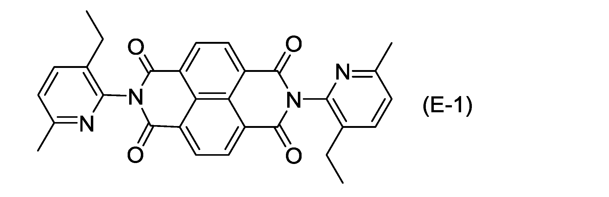
- the photosensitive layer contains, for example, a naphthalenetetracarboxylic acid diimide derivative having a structure represented by the chemical formula (E-1) as an electron transporting substance.
- Patent Document 1 the electrophotographic photoreceptor described in Patent Document 1 is insufficient in terms of sensitivity characteristics.
- the present invention has been made in view of the above problems, and an object thereof is to provide an electrophotographic photoreceptor having excellent sensitivity characteristics.
- the electrophotographic photoreceptor of the present invention comprises a conductive substrate and a single photosensitive layer.
- the photosensitive layer contains at least a charge generating agent and a compound represented by the general formula (1).
- Z represents a group represented by the following chemical formula (Z1) or a group represented by the following general formula (Z2).
- R 1, and R 1 in the general formula (Z2) of the general formula (1) optionally substituted carbon atoms be 6 to 22 aryl group, an alkyl group having 1 to 10 carbon atoms An aralkyl group having 7 to 20 carbon atoms, a cycloalkyl group having 3 to 20 carbon atoms, an alkoxy group having 1 to 6 carbon atoms, or a carbon atom which may be substituted with a -CO-OR 2 group. Represents an alkyl group having a number of 3 or more and 30 or less.
- R 2 represents an alkyl group having 1 to 8 carbon atoms.
- the electrophotographic photoreceptor of the present invention has excellent sensitivity characteristics.
- FIG. 3 is a partial cross-sectional view showing an example of the structure of the electrophotographic photosensitive member according to the embodiment of the present invention.
- FIG. 3 is a partial cross-sectional view showing an example of the structure of the electrophotographic photosensitive member according to the embodiment of the present invention.
- FIG. 3 is a partial cross-sectional view showing an example of the structure of the electrophotographic photosensitive member according to the embodiment of the present invention.
- a compound and a derivative thereof may be generically referred to by adding "system” after the compound name.
- a “system” is added after the compound name to represent the polymer name, it means that the repeating unit of the polymer is derived from the compound or its derivative.
- “—C 4 H 9 ”, “—C 6 H 13 ”, and “—COOEt” in the general formulas and chemical formulas respectively represent an n-butyl group, an n-hexyl group, and an ethoxycarbonyl group.
- the alkyl group having 1 to 10 carbon atoms, the alkyl group having 1 to 8 carbon atoms, the alkyl group having 1 to 6 carbon atoms, and the alkyl group having 1 to 3 carbon atoms are each a straight chain. It is in the form of a branched or branched chain and is unsubstituted.
- alkyl group having 1 to 10 carbon atoms examples include methyl group, ethyl group, n-propyl group, isopropyl group, n-butyl group, sec-butyl group, tert-butyl group, n-pentyl group, 1 -Methylbutyl group, 2-methylbutyl group, 3-methylbutyl group, 1-ethylpropyl group, 2-ethylpropyl group, 1,1-dimethylpropyl group, 1,2-dimethylpropyl group, 2,2-dimethylpropyl group, 1,2-dimethylpropyl group, n-hexyl group, 1-methylpentyl group, 2-methylpentyl group, 3-methylpentyl group, 4-methylpentyl group, 1,1-dimethylbutyl group, 1,2-dimethyl Butyl group, 1,3-dimethylbutyl group, 2,2-dimethylbutyl group, 2,3-dimethylbutyl group,
- Examples of the alkyl group having 1 to 8 carbon atoms are groups having 1 to 8 carbon atoms among the groups described as examples of the alkyl group having 1 to 10 carbon atoms.
- Examples of the alkyl group having 1 to 6 carbon atoms are groups having 1 to 6 carbon atoms among the groups described as examples of the alkyl group having 1 to 10 carbon atoms.
- Examples of the alkyl group having 1 to 3 carbon atoms are groups having 1 to 3 carbon atoms among the groups described as examples of the alkyl group having 1 to 10 carbon atoms.
- alkyl group having 3 to 30 carbon atoms an alkyl group having 3 to 15 carbon atoms, an alkyl group having 5 to 12 carbon atoms, an alkyl group having 5 carbon atoms, and an alkyl group having 12 carbon atoms, , Each of which is linear or branched and unsubstituted.
- the alkyl group having 3 to 30 carbon atoms is preferably an alkyl group having 3 to 15 carbon atoms.
- Examples of the alkyl group having 3 to 15 carbon atoms include the groups described above as examples of the alkyl group having 1 to 10 carbon atoms, which have 3 to 10 carbon atoms, straight-chain and branched groups.
- Examples of the alkyl group having 5 to 12 carbon atoms are groups having 5 to 12 carbon atoms among the groups described as examples of the alkyl group having 3 to 15 carbon atoms.
- Examples of the alkyl group having 5 carbon atoms are groups having 5 carbon atoms among the groups described as examples of the alkyl group having 3 to 15 carbon atoms.
- Examples of the alkyl group having 12 carbon atoms are groups having 12 carbon atoms among the groups described as examples of the alkyl group having 3 to 15 carbon atoms.
- the alkoxy group having 1 to 6 carbon atoms and the alkoxy group having 1 to 3 carbon atoms are linear or branched and unsubstituted.
- Examples of the alkoxy group having 1 to 6 carbon atoms include methoxy group, ethoxy group, n-propoxy group, isopropoxy group, n-butoxy group, sec-butoxy group, tert-butoxy group, n-pentoxy group, 1-methylbutoxy group, 2-methylbutoxy group, 3-methylbutoxy group, 1-ethylpropoxy group, 2-ethylpropoxy group, 1,1-dimethylpropoxy group, 1,2-dimethylpropoxy group, 2,2- Dimethylpropoxy group, 1,2-dimethylpropoxy group, n-hexyloxy group, 1-methylpentyloxy group, 2-methylpentyloxy group, 3-methylpentyloxy group, 4-methylpentyloxy group, 1,1- Dimethyl butoxy group, 1,2-dimethyl butoxy group, 1,3-dimethyl
- the aryl group having 6 to 22 carbon atoms, the aryl group having 6 to 14 carbon atoms, and the aryl group having 6 to 10 carbon atoms are each unsubstituted.
- Examples of the aryl group having 6 to 22 carbon atoms include phenyl group, naphthyl group, indacenyl group, biphenylenyl group, acenaphthylenyl group, anthryl group, phenanthryl group, tetracenyl group, tetraphenyl group, chrysenyl group, pyrenyl group, triphenylenyl group.
- aryl group having 6 to 14 carbon atoms examples include a phenyl group, a naphthyl group, an indacenyl group, a biphenylenyl group, an acenaphthylenyl group, an anthryl group, and a phenanthryl group.
- aryl group having 6 to 10 carbon atoms examples include a phenyl group and a naphthyl group.
- the cycloalkyl group having 3 to 20 carbon atoms and the cycloalkyl group having 3 to 10 carbon atoms are each unsubstituted.
- Examples of the cycloalkyl group having 3 to 20 carbon atoms include cyclopropyl group, cyclobutyl group, cyclopentyl group, cyclohexyl group, cycloheptyl group, cyclooctyl group, cyclononyl group, cyclodecyl group, cycloundecyl group, cyclododecyl group.
- cyclotridecyl group cyclotetradecyl group, cyclopentadecyl group, cyclohexadecyl group, cycloheptadecyl group, cyclooctadecyl group, cyclononadecyl group, and cycloicosanyl group.
- Examples of the cycloalkyl group having 3 to 10 carbon atoms are groups having 3 to 10 carbon atoms among the groups described as examples of the cycloalkyl group having 3 to 20 carbon atoms.
- the aralkyl group having 7 to 20 carbon atoms is unsubstituted.
- Examples of the aralkyl group having 7 to 20 carbon atoms include an alkyl group having 1 to 6 carbon atoms substituted with an aryl group having 6 to 14 carbon atoms.
- the definitions of the substituents used in the present specification have been described above.
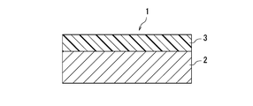
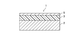
- FIG. 2 and FIG. 3 are partial cross-sectional views showing the structure of the photoconductor 1 which is an example of the present embodiment.
- the photoconductor 1 includes a conductive substrate 2 and a photosensitive layer 3.
- the photosensitive layer 3 is a single layer.
- the photosensitive layer 3 may be directly provided on the conductive substrate 2.
- the photoreceptor 1 may include, for example, a conductive substrate 2, an intermediate layer 4 (for example, an undercoat layer), and a photosensitive layer 3.
- the photosensitive layer 3 is provided on the conductive substrate 2 via the intermediate layer 4.
- the photosensitive layer 3 may be the outermost surface layer of the photoconductor 1.
- the photoconductor 1 may include a protective layer 5 as the outermost surface layer.
- the thickness of the photosensitive layer 3 is not particularly limited. The thickness of the photosensitive layer 3 is preferably 5 ⁇ m or more and 100 ⁇ m or less, and more preferably 10 ⁇ m or more and 50 ⁇ m or less.
- the structure of the photoconductor 1 has been described above with reference to FIGS. 1, 2, and 3.
- the photoreceptor according to the exemplary embodiment will be described in more detail.
- the photosensitive layer contains at least a charge generating agent and a compound represented by the general formula (1).
- the photosensitive layer may further contain a hole transport material.
- the photosensitive layer may further contain a binder resin.
- the photosensitive layer may further contain an additive, if necessary.
- the photosensitive layer contains a compound represented by the general formula (1) (hereinafter sometimes referred to as compound (1)).
- the photosensitive layer contains the compound (1) as an electron transfer material, for example.
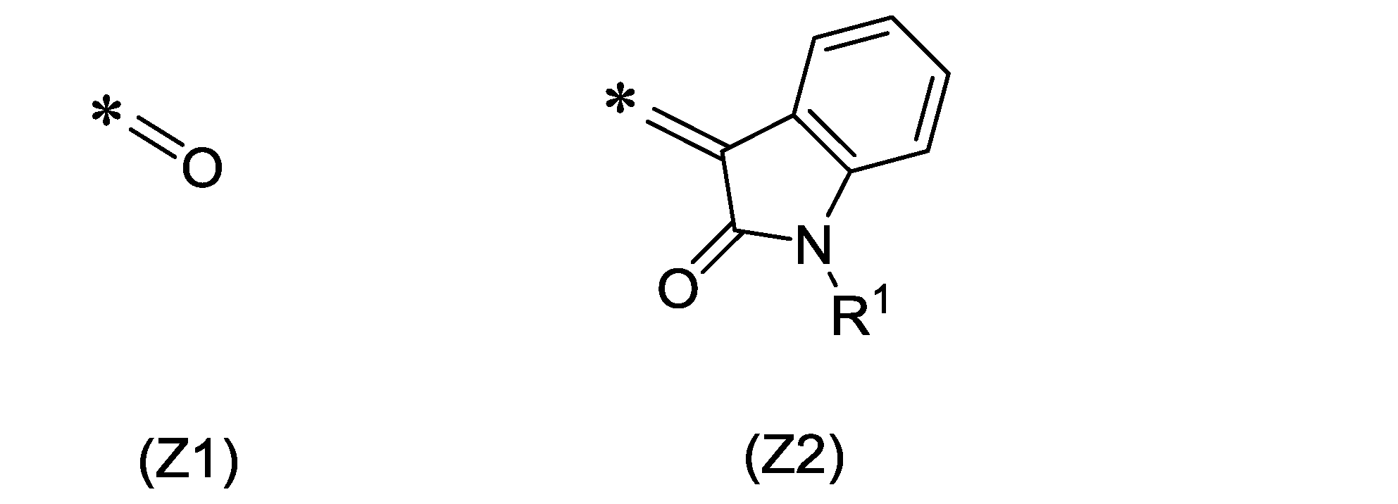
- Z represents a group represented by the following chemical formula (Z1) or a group represented by the following general formula (Z2).
- R 1 in the general formula (1) R 1, and the formula in (Z2) in the aryl group which 22 which may having 6 or more carbon atoms are less substituted with an alkyl group having 1 to 10 carbon atoms; atoms Aralkyl group having 7 to 20 carbon atoms; Cycloalkyl group having 3 to 20 carbon atoms; Alkoxy group having 1 to 6 carbon atoms; or 3 carbon atoms which may be substituted with -CO-OR 2 group It represents an alkyl group having 30 to 30 inclusive. In the —CO—OR 2 group, R 2 represents an alkyl group having 1 to 8 carbon atoms.
- the compound (1) By containing the compound (1) in the photosensitive layer, the sensitivity characteristics of the photoreceptor can be improved.
- the reason is presumed as follows.
- the compound (1) has a predetermined chemical structure containing four carbonyl groups which are electron accepting groups. Therefore, the compound (1) is excellent in electron accepting property and electron transporting property. Further, in the general formula (1), one tetracyclic condensed ring and one or two bicyclic condensed rings are bonded via a double bond. Therefore, the compound (1) has a wide planar structure. Since the compound (1) has a wide planar structure, the charge generating agent and the compound (1) overlap with each other, and the electron accepting property from the charge generating agent to the compound (1) is improved.
- the compound (1) since the compound (1) has a wide planar structure, the migration distance of electrons in the molecule of the compound (1) becomes long, and the electron transporting property is improved. Further, since the compound (1) has a wide planar structure, the overlap between the compounds (1) becomes large, and the electron transporting property between the molecules of the compound (1) is improved. Since the electron accepting property and the electron transporting property are improved as described above, the sensitivity characteristic of the photoconductor is improved.
- the aryl group having 6 to 22 carbon atoms represented by R 1 in the general formula (1) and R 1 in the general formula (Z2) is preferably an aryl group having 6 to 10 carbon atoms, and a phenyl group. Is more preferable.
- the aryl group having 6 to 22 carbon atoms represented by R 1 in the general formula (1) and R 1 in the general formula (Z2) may be substituted with an alkyl group having 1 to 10 carbon atoms.
- the alkyl group having 1 to 10 carbon atoms, which is a substituent of the aryl group having 6 to 22 carbon atoms, is preferably an alkyl group having 1 to 6 carbon atoms, and an alkyl group having 1 to 3 carbon atoms.
- a group is more preferable, and a methyl group and an ethyl group are even more preferable.
- the number of substituents (that is, an alkyl group having 1 to 10 carbon atoms) in the aryl group having 6 to 22 carbon atoms is preferably 1 or more and 5 or less, and is 1 or 2 It is more preferable that the number is 2, and it is further preferable that the number is 2.
- an aryl group having 6 to 22 carbon atoms When an aryl group having 6 to 22 carbon atoms is substituted with an alkyl group having 1 to 10 carbon atoms, an aryl group having 6 to 22 carbon atoms substituted with an alkyl group having 1 to 10 carbon atoms
- an aryl group having 6 to 10 carbon atoms substituted with an alkyl group having 1 to 6 carbon atoms is preferable, and a phenyl group substituted with an alkyl group having 1 to 3 carbon atoms is more preferable.
- an ethylmethylphenyl group is more preferable, and a 2-ethyl-6-methylphenyl group is particularly preferable.
- the aralkyl group having 7 to 20 carbon atoms represented by R 1 in the general formula (1) and R 1 in the general formula (Z2) is a carbon substituted with an aryl group having 6 to 14 carbon atoms.
- An alkyl group having 1 to 6 atoms is preferable, an alkyl group having 1 to 3 carbon atoms substituted with a phenyl group is more preferable, and a benzyl group is still more preferable.
- the cycloalkyl group having 3 to 20 carbon atoms represented by R 1 in the general formula (1) and R 1 in the general formula (Z2) is preferably a cycloalkyl group having 3 to 10 carbon atoms.
- the alkoxy group having 1 to 6 carbon atoms represented by R 1 in the general formula (1) and R 1 in the general formula (Z2) is preferably an alkoxy group having 1 to 3 carbon atoms.
- the alkyl group having 3 to 30 carbon atoms represented by R 1 in the general formula (1) and R 1 in the general formula (Z2) is preferably an alkyl group having 3 to 15 carbon atoms, and preferably a carbon atom.
- An alkyl group having 5 or more and 12 or less is more preferable, an alkyl group having 5 or 12 carbon atoms is further preferable, and a 2-butyloctyl group or a 3-methylbutyl group is particularly preferable.
- the alkyl group having 3 to 30 carbon atoms represented by R 1 in the general formula (1) and R 1 in the general formula (Z2) may be substituted with a —CO—OR 2 group.
- R 2 represents an alkyl group having 1 to 8 carbon atoms.
- the alkyl group having 1 to 8 carbon atoms represented by R 2 is preferably an alkyl group having 1 to 3 carbon atoms, and more preferably an ethyl group.
- the number of substituents (that is, —CO—OR 2 group) in the alkyl group having 3 to 30 carbon atoms represented by R 1 is preferably 1 to 5 and preferably 1 to 3 Is more preferable, and one is still more preferable.
- an alkyl group having 3 to 30 carbon atoms is substituted with -CO-OR 2 group, the substituted carbon atom number of 3 to 30 alkyl group -CO-OR 2 group, -CO-OR
- An alkyl group having 5 to 12 carbon atoms substituted with 2 groups preferably —CO—OR 2 group in which R 2 represents an alkyl group having 1 to 3 carbon atoms, more preferably ethoxycarbonyl group
- R 2 represents an alkyl group having 1 to 3 carbon atoms, more preferably ethoxycarbonyl group
- An alkyl group having 5 carbon atoms substituted with an ethoxycarbonyl group is more preferable, and a 1-ethoxycarbonyl-3-methylbutyl group is still more preferable.
- R 1 of R 1, and the general formula (Z2) in in may be substituted with an alkyl group having 1 to 10 carbon atoms It is preferable to represent an aryl group having 6 to 22 carbon atoms; an aralkyl group having 7 to 20 carbon atoms; or an alkyl group having 3 to 30 carbon atoms which may be substituted with a —CO—OR 2 group.
- R 2 preferably represents an alkyl group having 1 to 8 carbon atoms.
- R 1 in the general formula (1) R 1, and the formula in (Z2) in the good carbon atoms optionally substituted by a -CO-OR 2 group It is preferable to represent 3 or more and 30 or less alkyl groups.
- R 2 preferably represents an alkyl group having 1 to 8 carbon atoms.
- R 1 is a long-chain alkyl group such as an alkyl group having 3 to 30 carbon atoms
- the long-chain alkyl group contained in the compound (1) is entangled with the main chain of the binder resin, and the binder resin and the compound It is considered that the compatibility with (1) is improved. Therefore, the compound (1) is uniformly dispersed in the photosensitive layer, and the sensitivity characteristics of the photoconductor are further improved.
- Z in the general formula (1) is a group represented by the chemical formula (Z1)
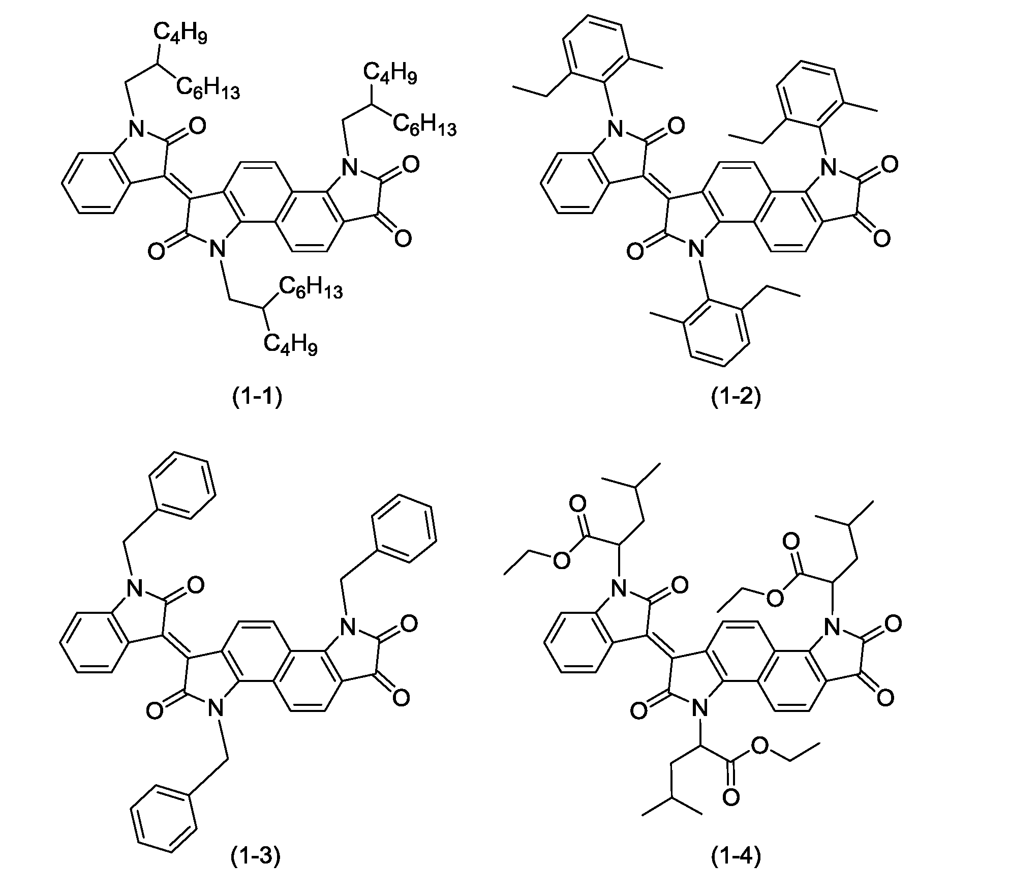
- preferable examples of the compound (1) include the chemical formulas (1-1), (1-2) and (1-3).
- a compound represented by (1-4) hereinafter, each may be referred to as compound (1-1), (1-2), (1-3), and (1-4)) Is mentioned.
- the compound (1-5) is particularly preferably the compound (1-5).
- Z in the general formula (1) is a group represented by the general formula (Z2)
- preferred examples of the compound (1) include chemical formulas (1-5), (1-6), (1- 7) and compounds represented by (1-8) (hereinafter, referred to as compounds (1-5), (1-6), (1-7), and (1-8), respectively. ) Is mentioned.
- the photosensitive layer may contain only one type of compound (1) or may contain two or more types of compound (1).
- the photosensitive layer may contain only the compound (1) as an electron transfer agent, and in addition to the compound (1), an electron transfer agent other than the compound (1) (hereinafter referred to as other electron transfer agent). There is further).
- other electron transfer agents include quinone compounds, diimide compounds, hydrazone compounds, thiopyran compounds, trinitrothioxanthone compounds, 3,4,5,7-tetranitro-9-fluorenone compounds, dinitroanthracene compounds.
- Examples thereof include compounds, dinitroacridine compounds, tetracyanoethylene, 2,4,8-trinitrothioxanthone, dinitrobenzene, dinitroacridine, succinic anhydride, maleic anhydride, and dibromomaleic anhydride.
- Examples of quinone compounds include diphenoquinone compounds, azoquinone compounds, anthraquinone compounds, naphthoquinone compounds, nitroanthraquinone compounds, and dinitroanthraquinone compounds.
- the content of the compound (1) is preferably 5 parts by mass or more and 100 parts by mass or less, and more preferably 20 parts by mass or more and 40 parts by mass or less with respect to 100 parts by mass of the binder resin.
- the content of the compound (1) is 5 parts by mass or more based on 100 parts by mass of the binder resin, it is easy to improve the sensitivity characteristics of the photoreceptor.
- the content of the compound (1) is 100 parts by mass or less based on 100 parts by mass of the binder resin, the compound (1) is easily dissolved in the solvent for forming the photosensitive layer, and a uniform photosensitive layer is easily formed.
- Compound (1) is produced, for example, according to a reaction represented by the following reaction formula (R-1) (hereinafter sometimes referred to as reaction (R-1)), or a method analogous thereto.
- reaction (R-1) a reaction represented by the following reaction formula (R-1)
- reaction (R-1) the compounds represented by the general formulas (A) and (B) represented by the reaction formula (R-1) are referred to as compounds (A) and (B), respectively.
- R 1 in the general formula (A) and (B) is a general formula (1) and the same meaning as R 1 in formula (Z2) in.
- the reaction (R-1) may be performed under an inert gas atmosphere.
- the inert gas include nitrogen gas and argon gas.
- the reaction temperature of the reaction (R-1) is preferably 50 ° C. or higher and 180 ° C. or lower.
- the reaction time of the reaction (R-1) is preferably 5 hours or more and 20 hours or less. The case where the compound (1) in which Z is a group represented by the chemical formula (Z1) is produced has been described above.
- Suitable examples of the acid catalyst, the solvent, the inert gas, and the reaction temperature are the same as those for producing the compound (1) in which Z is a group represented by the chemical formula (Z1).
- the reaction time of the reaction (R-1) is preferably 10 hours or longer and 30 hours or shorter.
- a dehydrating agent may be further added.
- An example of a dehydrating agent is diphosphorus pentoxide. The case where the compound (1) in which Z is a group represented by the general formula (Z2) is produced has been described above.
- the compound (A) used in the reaction (R-1) can be prepared, for example, according to the reaction represented by the following reaction formula (R-0) (hereinafter sometimes referred to as reaction (R-0)). Alternatively, it is manufactured by a method similar to this.
- reaction (R-0) the reaction represented by the following reaction formula (R-0)
- R-0 the reaction represented by the following reaction formula (R-0)
- reaction (D) the compounds represented by the chemical formula (C) represented by the reaction formula (R-0) and the general formula (D) are referred to as compounds (C) and (D), respectively.
- R 1 in the general formula (D) is a general formula (1) and the same meaning as R 1 in formula (Z2) in.
- reaction (R-0) 1 molar equivalent of the compound (C) is reacted with 2 molar equivalents of the compound (D) to obtain 1 molar equivalent of the compound (A).
- compound (C) and compound (D) are stirred in a solvent in the presence of a base.
- bases include potassium carbonate, sodium carbonate, and potassium phosphate.
- solvents include N, N-dimethylformamide, and tetrahydrofuran.
- the reaction (R-0) is preferably performed in an inert gas atmosphere. Examples of the inert gas include nitrogen gas and argon gas.
- the reaction temperature of the reaction (R-0) is preferably 50 ° C. or higher and 150 ° C. or lower.
- the reaction time of the reaction (R-0) is preferably 0.5 hours or more and 5 hours or less.
- the charge generating agent is not particularly limited as long as it is a charge generating agent for a photoreceptor.
- the charge generating agent include phthalocyanine pigments, perylene pigments, bisazo pigments, trisazo pigments, dithioketopyrrolopyrrole pigments, metal-free naphthalocyanine pigments, metal naphthalocyanine pigments, squaraine pigments, indigo pigments, azurenium pigments, cyanines.
- Pigments powders of inorganic photoconductive materials (for example, selenium, selenium-tellurium, selenium-arsenic, cadmium sulfide or amorphous silicon), pyrylium pigments, ansanthuron pigments, triphenylmethane pigments, slene pigments, toluidine pigments, Examples include pyrazoline-based pigments and quinacridone-based pigments.
- the photosensitive layer may contain only one type of charge generating agent, or may contain two or more types of charge generating agents.
- phthalocyanine pigments include metal-free phthalocyanine and metal phthalocyanine.
- the metal-free phthalocyanine is represented by the chemical formula (CGM2).
- the metal phthalocyanine include titanyl phthalocyanine, hydroxygallium phthalocyanine, and chlorogallium phthalocyanine.
- Titanyl phthalocyanine is represented by a chemical formula (CGM1).
- the phthalocyanine pigment may be crystalline or non-crystalline.
- the crystal shape of the phthalocyanine-based pigment (for example, ⁇ -type, ⁇ -type, Y-type, V-type, or II-type) is not particularly limited, and phthalocyanine-based pigments having various crystal shapes can be used.
- Examples of the metal-free phthalocyanine crystals include X-type crystals of metal-free phthalocyanine (hereinafter, sometimes referred to as X-type metal-free phthalocyanine).
- Examples of the crystal of titanyl phthalocyanine include ⁇ -type, ⁇ -type, and Y-type crystals of titanyl phthalocyanine (hereinafter sometimes referred to as ⁇ -type, ⁇ -type, and Y-type titanyl phthalocyanine).
- the charge generating agent is preferably a phthalocyanine-based pigment, more preferably metal-free phthalocyanine or titanyl phthalocyanine, and further preferably X-type metal-free phthalocyanine or Y-type titanyl phthalocyanine.
- Y-type titanyl phthalocyanine is particularly preferable.
- Y-type titanyl phthalocyanine has a main peak at 27.2 ° of Bragg angle (2 ⁇ ⁇ 0.2 °) in the CuK ⁇ characteristic X-ray diffraction spectrum.
- the main peak in the CuK ⁇ characteristic X-ray diffraction spectrum is a peak having the first or second highest intensity in the range where the Bragg angle (2 ⁇ ⁇ 0.2 °) is 3 ° or more and 40 ° or less.
- a sample (titanyl phthalocyanine) is filled in a sample holder of an X-ray diffractometer (for example, “RINT (registered trademark) 1100” manufactured by Rigaku Corporation), and an X-ray tube Cu, a tube voltage of 40 kV, a tube current of 30 mA, and CuK ⁇ .
- An X-ray diffraction spectrum is measured under the condition that the characteristic X-ray wavelength is 1.542 ⁇ .
- the measurement range (2 ⁇ ) is, for example, 3 ° or more and 40 ° or less (start angle 3 °, stop angle 40 °), and the scanning speed is, for example, 10 ° / min.
- Ananthanthrone pigment is preferably used as a charge generating agent in a photoreceptor applied to an image forming apparatus using a short wavelength laser light source (for example, a laser light source having a wavelength of 350 nm or more and 550 nm or less).
- a short wavelength laser light source for example, a laser light source having a wavelength of 350 nm or more and 550 nm or less.
- the content of the charge generating agent is preferably 0.1 parts by mass or more and 50 parts by mass or less, and more preferably 0.5 parts by mass or more and 30 parts by mass or less, with respect to 100 parts by mass of the binder resin. It is particularly preferable that the amount is 0.5 parts by mass or more and 4.5 parts by mass or less.
- hole transfer agent examples include triphenylamine derivatives, diamine derivatives (eg, N, N, N ′, N′-tetraphenylbenzidine derivatives, N, N, N ′, N′-tetraphenylphenylenediamine derivatives, N, N, N ', N'-tetraphenylnaphthylenediamine derivative, N, N, N', N'-tetraphenylphenanthrylenediamine derivative, and di (aminophenylethenyl) benzene derivative), oxadiazole Compounds (eg 2,5-di (4-methylaminophenyl) -1,3,4-oxadiazole), styryl compounds (eg 9- (4-diethylaminostyryl) anthracene), carbazole compounds ( For example, polyvinylcarbazole), organic polysilane compound, pyrazoline compound (eg, 1-phenyl-3), pyrazoline compound (
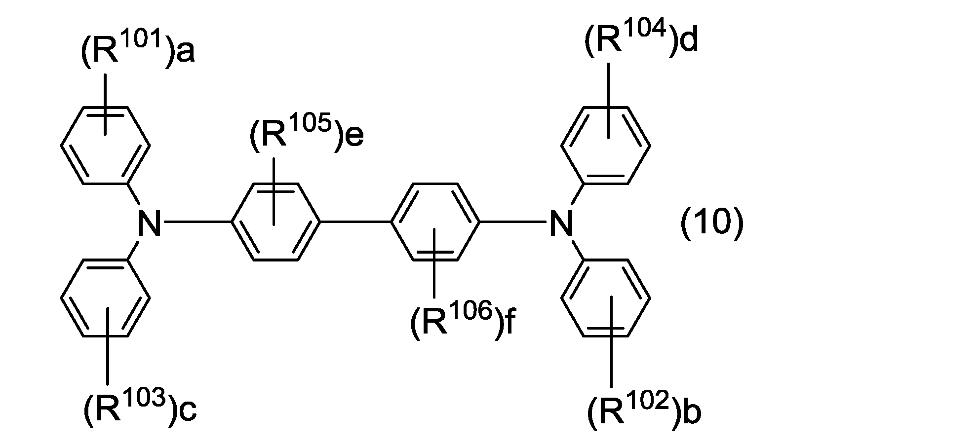
- the photosensitive layer preferably contains a compound represented by the general formula (10) (hereinafter sometimes referred to as compound (10)).
- the photosensitive layer preferably contains, for example, the compound (10) as a hole transport material.
- R 101 , R 102 , R 103 , R 104 , R 105 , and R 106 each independently represent an alkyl group having 1 to 6 carbon atoms, and an alkyl group having 1 to 6 carbon atoms. It represents an alkoxy group or an aryl group having 6 to 14 carbon atoms.
- a, b, c, and d each independently represent an integer of 0 or more and 5 or less.
- e and f each independently represent an integer of 0 or more and 4 or less.
- a represents an integer of 2 or more and 5 or less
- a plurality of R 101 may be the same or different from each other.
- b represents an integer of 2 or more and 5 or less
- a plurality of R 102 may be the same or different from each other.
- c represents an integer of 2 or more and 5 or less
- a plurality of R 103 may be the same as or different from each other.
- d represents an integer of 2 or more and 5 or less
- a plurality of R 104 may be the same or different from each other.
- e represents an integer of 2 or more and 4 or less
- a plurality of R 105 s may be the same as or different from each other.
- f represents an integer of 2 or more and 4 or less
- a plurality of R 106 may be the same or different from each other.
- R 101 , R 102 , R 103 , R 104 , R 105 , and R 106 each independently preferably represent an alkyl group having 1 to 6 carbon atoms, and the number of carbon atoms. It is more preferable to represent 1 to 3 alkyl groups, and it is even more preferable to represent a methyl group. It is preferable that each of a, b, c and d independently represents 0 or 1, and more preferably 1. e and f each independently represent 0 or 1, and more preferably represent 1.
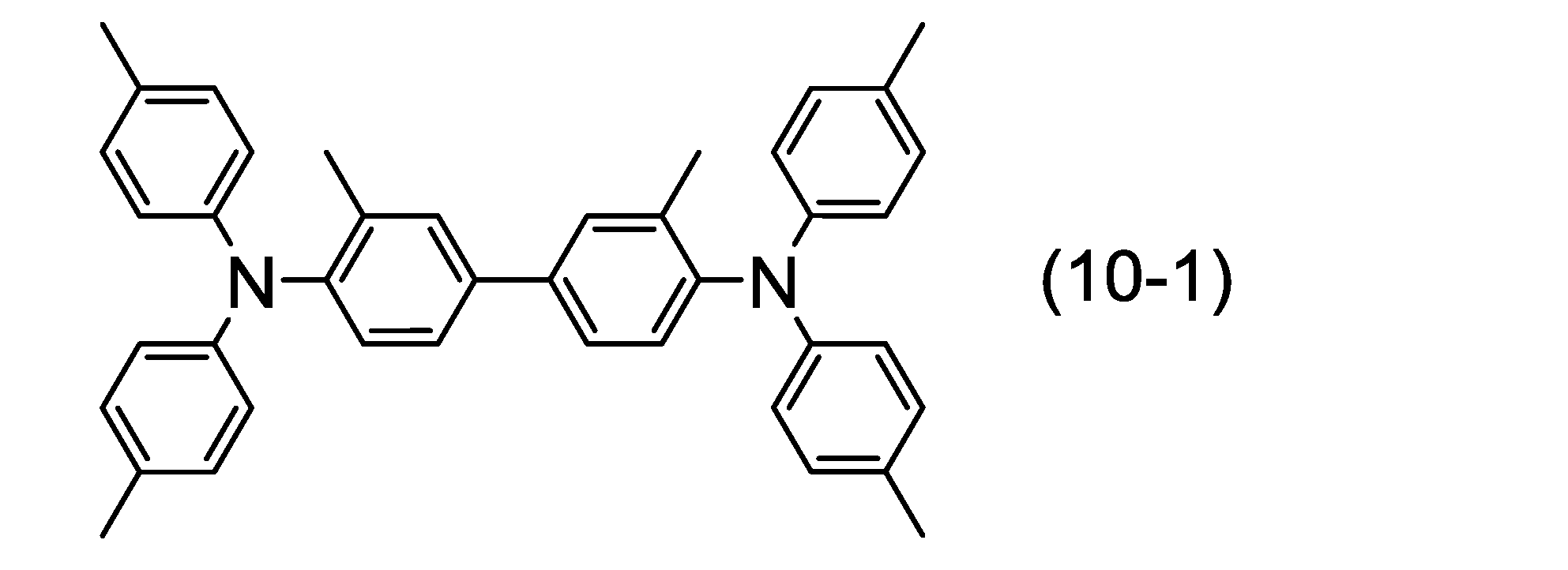
- a preferable example of the compound (10) includes a compound represented by the following chemical formula (10-1) (hereinafter sometimes referred to as compound (10-1)).
- the photosensitive layer may contain only the compound (10) as a hole transport material.
- the photosensitive layer may further contain a hole transporting agent other than the compound (10) as a hole transporting agent.
- the content of the hole transport material is preferably 10 parts by mass or more and 200 parts by mass or less, and more preferably 10 parts by mass or more and 100 parts by mass or less with respect to 100 parts by mass of the binder resin.
- binder resin examples include thermoplastic resins, thermosetting resins, and photocurable resins.
- thermoplastic resin examples include polycarbonate resin, polyarylate resin, styrene-butadiene copolymer, styrene-acrylonitrile copolymer, styrene-maleic acid copolymer, acrylic acid polymer, styrene-acrylic acid copolymer, Polyethylene resin, ethylene-vinyl acetate copolymer, chlorinated polyethylene resin, polyvinyl chloride resin, polypropylene resin, ionomer resin, vinyl chloride-vinyl acetate copolymer, alkyd resin, polyamide resin, urethane resin, polysulfone resin, diallyl phthalate Examples include resins, ketone resins, polyvinyl butyral resins, polyester resins, and polyether resins.
- thermosetting resin examples include silicone resin, epoxy resin, phenol resin, urea resin, and melamine resin.
- photocurable resin examples include acrylic acid adducts of epoxy compounds and acrylic acid adducts of urethane compounds.
- the photosensitive layer may contain only one kind of binder resin, or may contain two or more kinds of binder resin.
- a polycarbonate resin is preferable as the binder resin because a photosensitive layer having an excellent balance of processability, mechanical characteristics, optical characteristics, and abrasion resistance can be obtained.
- the polycarbonate resin include bisphenol ZC type polycarbonate resin, bisphenol C type polycarbonate resin, bisphenol A type polycarbonate resin, and bisphenol Z type polycarbonate resin.
- the bisphenol Z type polycarbonate resin has a repeating unit represented by the following chemical formula (20).
- a polycarbonate resin having a repeating unit represented by the chemical formula (20) may be referred to as a polycarbonate resin (20).
- the polycarbonate resin (20) preferably has only the repeating unit (20) as a repeating unit.
- additives examples include deterioration inhibitors (eg, antioxidants, radical scavengers, singlet quenchers or ultraviolet absorbers), softeners, surface modifiers, extenders, thickeners, dispersion stabilizers. , Waxes, acceptors, donors, surfactants, plasticizers, sensitizers, and leveling agents.
- deterioration inhibitors eg, antioxidants, radical scavengers, singlet quenchers or ultraviolet absorbers
- softeners surface modifiers
- extenders extenders
- thickeners thickeners
- dispersion stabilizers dispersion stabilizers.
- Waxes acceptors, donors, surfactants, plasticizers, sensitizers, and leveling agents.
- the material contained in the photosensitive layer is preferably any one of the following combinations.
- the electron transfer agent is a compound (1-1), (1-2), (1-3), (1-4), (1-5), (1-6), (1-7). ) Or (1-8), and the hole-transporting agent includes the compound (10-1).
- the electron transfer agent is a compound (1-1), (1-2), (1-3), (1-4), (1-5), (1-6), (1-7).
- the binder contains a polycarbonate resin (20).
- the electron transfer agent is a compound (1-1), (1-2), (1-3), (1-4), (1-5), (1-6), (1-7).
- the electron transfer agent includes X-type metal-free phthalocyanine.
- the electron transfer agent is a compound (1-1), (1-2), (1-3), (1-4), (1-5), (1-6), (1-7).
- the charge generating agent includes Y-type titanyl phthalocyanine.
- the electron transfer agent is a compound (1-1), (1-2), (1-3), (1-4), (1-5), (1-6), (1-7).
- the hole-transporting agent contains the compound (10-1), and the binder contains the polycarbonate resin (20).
- the electron transfer agent is a compound (1-1), (1-2), (1-3), (1-4), (1-5), (1-6), (1-7).
- the hole transporting agent contains the compound (10-1), the binder contains the polycarbonate resin (20), and the charge generating agent contains the X-type metal-free phthalocyanine.
- the electron transfer agent is a compound (1-1), (1-2), (1-3), (1-4), (1-5), (1-6), (1-7).
- the hole transport material contains the compound (10-1), the binder contains the polycarbonate resin (20), and the charge generation material contains Y-type titanyl phthalocyanine.
- At least the surface portion of the conductive substrate may be made of a material having conductivity.
- An example of the conductive base is a conductive base made of a material having conductivity.
- Another example of the conductive substrate is a conductive substrate coated with a material having conductivity.
- the material having conductivity include aluminum, iron, copper, tin, platinum, silver, vanadium, molybdenum, chromium, cadmium, titanium, nickel, palladium, indium, stainless steel, and brass.
- One of these electrically conductive materials may be used alone, or two or more thereof may be used in combination (for example, as an alloy).
- aluminum or aluminum alloy is preferable because the transfer of charges from the photosensitive layer to the conductive substrate is good.
- the shape of the conductive substrate is appropriately selected according to the structure of the image forming apparatus.
- Examples of the shape of the conductive substrate include a sheet shape and a drum shape.
- the thickness of the conductive substrate is appropriately selected according to the shape of the conductive substrate.
- the intermediate layer (undercoat layer) contains, for example, inorganic particles and a resin used for the intermediate layer (resin for intermediate layer). Due to the presence of the intermediate layer, the flow of current generated when the photosensitive member is exposed is smoothed and the increase in resistance is suppressed while maintaining the insulation state to the extent that leakage can be suppressed.
- the inorganic particles include particles of metal (for example, aluminum, iron, or copper), particles of metal oxide (for example, titanium oxide, alumina, zirconium oxide, tin oxide, or zinc oxide), and non-metal oxides. (Eg silica) particles. These inorganic particles may be used alone or in combination of two or more.
- the example of the resin for the intermediate layer is the same as the example of the binder resin contained in the photosensitive layer.
- the intermediate layer may contain an additive as needed.
- the examples of the additives contained in the intermediate layer are the same as the examples of the additives contained in the photosensitive layer.
- the photoconductor is produced, for example, by applying a coating solution for forming a photosensitive layer (hereinafter, also referred to as a coating solution) on a conductive substrate and drying.
- the coating liquid is produced by dissolving or dispersing the charge generating agent, the compound (1), and the components (for example, the hole transporting agent, the binder resin, and the additive), which are added as necessary, in the solvent. .
- the solvent contained in the coating liquid is not particularly limited as long as it can dissolve or disperse each component contained in the coating liquid.
- solvents are alcohols (eg methanol, ethanol, isopropanol or butanol), aliphatic hydrocarbons (eg n-hexane, octane or cyclohexane), aromatic hydrocarbons (eg benzene, toluene or xylene), Halogenated hydrocarbons (for example, dichloromethane, dichloroethane, carbon tetrachloride or chlorobenzene), ethers (for example, dimethyl ether, diethyl ether, tetrahydrofuran, ethylene glycol dimethyl ether, diethylene glycol dimethyl ether or propylene glycol monomethyl ether), ketones (for example, acetone, Methyl ethyl ketone or cyclohexanone), esters (eg ethyl acetate or
- the coating liquid is prepared by mixing the components and dispersing them in a solvent.
- a bead mill, roll mill, ball mill, attritor, paint shaker, or ultrasonic disperser can be used.
- the coating liquid may contain, for example, a surfactant in order to improve the dispersibility of each component.
- the method of applying the coating liquid is not particularly limited as long as it is a method capable of uniformly applying the coating liquid onto the conductive substrate.
- Examples of the coating method include a blade coating method, a dip coating method, a spray coating method, a spin coating method, and a bar coating method.
- the method for drying the coating liquid is not particularly limited as long as the solvent in the coating liquid can be evaporated.
- a method of heat treatment hot air drying
- the heat treatment temperature is, for example, a temperature of 40 ° C. or higher and 150 ° C. or lower.
- the heat treatment time is, for example, 3 minutes or more and 120 minutes or less.
- the method for producing the photoreceptor may further include one or both of the step of forming the intermediate layer and the step of forming the protective layer, if necessary.
- the step of forming the intermediate layer and the step of forming the protective layer known methods are appropriately selected.
- ⁇ Material for forming photosensitive layer> As materials for forming the photosensitive layer of the photoreceptor, the following charge generating agent, hole transporting agent, binder resin, and electron transporting agent were prepared.
- Y-type titanyl phthalocyanine and X-type metal-free phthalocyanine were prepared as charge generating agents.
- the Y-type titanyl phthalocyanine was represented by the chemical formula (CGM1) described in the embodiment and was a titanyl phthalocyanine having a Y-type crystal structure.
- the X-type metal-free phthalocyanine was a metal-free phthalocyanine represented by the chemical formula (CGM2) described in the embodiment and having an X-type crystal structure.
- Binder resin As the binder resin, the polycarbonate resin (20) described in the embodiment was prepared.
- the viscosity average molecular weight of the polycarbonate resin (20) was 50,000.
- each of the compounds (1-1) to (1-8) described in the embodiment was synthesized by the following method. The yield of each compound was determined by conversion into molar ratio.
- reaction (r-1a) (Synthesis of Compound (1-1))
- Compound (1-1) was synthesized according to the reaction represented by the following reaction formula (r-1a) (hereinafter referred to as reaction (r-1a)).
- the compounds (A-1) to (A-4) and (B-1) to (B-4) described below are respectively represented by the chemical formula (A-1) and the chemical formula (A-1) in the reaction formula (r-1a). It is represented by (B-1) and the chemical formulas (A-2) to (A-4) and (B-1) to (B-4) described later.
- a compound (1-1) was obtained by reacting about 1 molar equivalent of the compound (A-1) with about 1 molar equivalent of the compound (B-1). Specifically, the compound (A-1) (0.656 g, 1.09 mmol) and paratoluenesulfonic acid monohydrate (38 mg, 0.199 mmol) were dissolved in n-butyric acid (10 mL), A solution was obtained. After heating the solution to 130 ° C., the compound (B-1) (0.287 g, 0.955 mmol) was added dropwise to the solution. After the dropping, the solution was stirred at 130 ° C. for 16 hours. The solution was then cooled to room temperature.
- the compounds (A-2) to (A-4) and (B-2) to (B-4) are represented by the following chemical formulas (A-2) to (A-4) and (B-2) to, respectively. It is represented by (B-4).
- a compound represented by the following chemical formula (E-1) (hereinafter referred to as compound (E-1)) was prepared as an electron transfer agent used in Comparative Examples.
- Photoreceptors (A-1) to (A-16) and (B-1) to (B-2) were produced using the materials for forming the photosensitive layer.
- the compound (1-1) was used as the electron transfer agent in the production of the photoconductor (A-1), but the photoconductors (A-2) to (A-16) and (B-1) to (B-2) were used.
- the electron transfer agents of the types shown in Table 3 were used in the respective productions of (a).
- ⁇ Evaluation of sensitivity characteristics The sensitivity characteristics of each of the photoreceptors (A-1) to (A-16) and (B-1) to (B-2) were evaluated. The evaluation of the sensitivity characteristics was performed in an environment of a temperature of 23 ° C. and a relative humidity of 50% RH. First, the surface of the photoconductor was charged to +600 V using a drum sensitivity tester (manufactured by Gentec Co., Ltd.). Then, using a bandpass filter, monochromatic light (wavelength 780 nm, half width 20 nm, light energy 1.5 ⁇ J / cm 2 ) was extracted from the white light of the halogen lamp. The extracted monochromatic light was applied to the surface of the photoreceptor.
- the surface potential of the photoreceptor was measured when 50 milliseconds had elapsed after the irradiation was completed. The measured surface potential was used as the potential after exposure ( VL , unit: + V).
- the post-exposure potential ( VL ) of the photoconductor is shown in Table 3. It should be noted that the smaller the post-exposure potential ( VL ) is, the more positive the sensitivity value (more specifically, the photosensitivity characteristic) of the photoconductor is.
- CGM, ETM, V L , X-H 2 Pc, and Y-TiOPc represent a charge generating agent, an electron transfer agent, a post-exposure potential, an X-type metal-free phthalocyanine, and a Y-type titanyl phthalocyanine, respectively.
- “None” indicates that a crystallized portion was not confirmed in the photosensitive layer, and "Slightly crystallized” indicates that a crystallized portion was slightly confirmed in the photosensitive layer.
- the photoconductors (A-1) to (A-16) each had a conductive base and a single photosensitive layer.
- the photosensitive layer contained at least the charge generating agent and the compound (1).
- the photosensitive layer contained any of the compounds (1-1) to (1-8) included in the general formula (1).
- the post-exposure potential of the photoconductors (A-1) to (A-16) was + 108V or less. In the photosensitive layers of the photoconductors (A-1) to (A-16), no crystallized part was confirmed.
- the photosensitive layers of the photoconductors (B-1) to (B-2) did not contain the compound (1). Specifically, the photosensitive layers of the photoconductors (B-1) to (B-2) contained the compound (E-1), but the compound (E-1) is included in the general formula (1). It wasn't a compound. As is clear from Table 3, the post-exposure potential of the photoconductors (B-1) to (B-2) was + 130V or higher. In the photosensitive layers of the photoconductors (B-1) to (B-2), some crystallized parts were confirmed.
- the photoconductors (A-1) to (A-16) were superior in sensitivity characteristics to the photoconductors (B-1) to (B-2). Further, the photoconductors (A-1) to (A-16) are superior in sensitivity characteristics to the photoconductors (B-1) to (B-2) and suppress crystallization of the photosensitive layer. It had been.
- the photoconductor according to the present invention can be used in an image forming apparatus.
Landscapes
- Physics & Mathematics (AREA)
- General Physics & Mathematics (AREA)
- Photoreceptors In Electrophotography (AREA)
Abstract
電子写真感光体は、導電性基体と、単層の感光層とを備える。感光層は、電荷発生剤と、一般式(1)で表される化合物とを少なくとも含有する。一般式(1)中、Zは、化学式(Z1)又は一般式(Z2)で表される基を表す。一般式(1)及び(Z2)中のR1は、C1-10アルキル基で置換されてもよいC6-22アリール基、C7-20アラルキル基、C3-20シクロアルキル基、C1-6アルコキシ基、又は-CO-OR2基で置換されてもよいC3-30アルキル基を表す。R2は、C1-8アルキル基を表す。
Description
本発明は、電子写真感光体に関する。
電子写真感光体は、電子写真方式の画像形成装置に用いられる。電子写真感光体としては、例えば、積層型電子写真感光体又は単層型電子写真感光体が用いられる。積層型電子写真感光体は、感光層として、電荷発生の機能を有する電荷発生層と、電荷輸送の機能を有する電荷輸送層とを備える。単層型電子写真感光体は、感光層として、電荷発生の機能と電荷輸送の機能とを有する単層の感光層を備える。
特許文献1に記載の電子写真感光体は、感光層を含む。この感光層は、電子輸送物質として、例えば、化学式(E-1)で示される構造を有するナフタレンテトラカルボン酸ジイミド誘導体を含む。
しかし、特許文献1に記載の電子写真感光体は感度特性の点で不十分であることが、本発明者の検討により判明した。
本発明は、上記課題に鑑みてなされたものであり、その目的は、感度特性に優れる電子写真感光体を提供することである。
本発明の電子写真感光体は、導電性基体と、単層の感光層とを備える。前記感光層は、電荷発生剤と、一般式(1)で表される化合物とを少なくとも含有する。
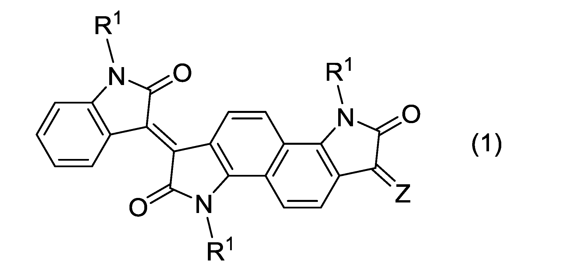
前記一般式(1)中、Zは、下記化学式(Z1)で表される基、又は下記一般式(Z2)で表される基を表す。前記一般式(1)中のR1、及び前記一般式(Z2)中のR1は、炭素原子数1以上10以下のアルキル基で置換されてもよい炭素原子数6以上22以下のアリール基、炭素原子数7以上20以下のアラルキル基、炭素原子数3以上20以下のシクロアルキル基、炭素原子数1以上6以下のアルコキシ基、又は-CO-OR2基で置換されてもよい炭素原子数3以上30以下のアルキル基を表す。R2は、炭素原子数1以上8以下のアルキル基を表す。

本発明の電子写真感光体は、感度特性に優れる。
以下、本発明の実施形態について詳細に説明する。しかし、本発明は、以下の実施形態に何ら限定されない。本発明は、本発明の目的の範囲内で、適宜変更を加えて実施できる。なお、説明が重複する箇所については、適宜説明を省略する場合があるが、発明の要旨は限定されない。
以下、化合物名の後に「系」を付けて、化合物及びその誘導体を包括的に総称する場合がある。また、化合物名の後に「系」を付けて重合体名を表す場合には、重合体の繰返し単位が化合物又はその誘導体に由来することを意味する。また、一般式及び化学式中の「-C4H9」、「-C6H13」、及び「-COOEt」は、各々、n-ブチル基、n-ヘキシル基、及びエトキシカルボニル基を表す。
次に、本明細書において用いられる置換基の定義について説明する。炭素原子数1以上10以下のアルキル基、炭素原子数1以上8以下のアルキル基、炭素原子数1以上6以下のアルキル基、及び炭素原子数1以上3以下のアルキル基は、各々、直鎖状又は分枝鎖状で非置換である。炭素原子数1以上10以下のアルキル基としては、例えば、メチル基、エチル基、n-プロピル基、イソプロピル基、n-ブチル基、sec-ブチル基、tert-ブチル基、n-ペンチル基、1-メチルブチル基、2-メチルブチル基、3-メチルブチル基、1-エチルプロピル基、2-エチルプロピル基、1,1-ジメチルプロピル基、1,2-ジメチルプロピル基、2,2-ジメチルプロピル基、1,2-ジメチルプロピル基、n-ヘキシル基、1-メチルペンチル基、2-メチルペンチル基、3-メチルペンチル基、4-メチルペンチル基、1,1-ジメチルブチル基、1,2-ジメチルブチル基、1,3-ジメチルブチル基、2,2-ジメチルブチル基、2,3-ジメチルブチル基、3,3-ジメチルブチル基、1,1,2-トリメチルプロピル基、1,2,2-トリメチルプロピル基、1-エチルブチル基、2-エチルブチル基、3-エチルブチル基、直鎖状及び分枝鎖状のヘプチル基、直鎖状及び分枝鎖状のオクチル基、直鎖状及び分枝鎖状のノニル基、並びに直鎖状及び分枝鎖状のデシル基が挙げられる。炭素原子数1以上8以下のアルキル基の例は、炭素原子数1以上10以下のアルキル基の例として述べた基のうち、炭素原子数が1以上8以下である基である。炭素原子数1以上6以下のアルキル基の例は、炭素原子数1以上10以下のアルキル基の例として述べた基のうち、炭素原子数が1以上6以下である基である。炭素原子数1以上3以下のアルキル基の例は、炭素原子数1以上10以下のアルキル基の例として述べた基のうち、炭素原子数が1以上3以下である基である。
炭素原子数3以上30以下のアルキル基、炭素原子数3以上15以下のアルキル基、炭素原子数5以上12以下のアルキル基、炭素原子数5のアルキル基、及び炭素原子数12のアルキル基は、各々、直鎖状又は分枝鎖状で非置換である。炭素原子数3以上30以下のアルキル基として好ましくは、炭素原子数3以上15以下のアルキル基である。炭素原子数3以上15以下のアルキル基の例は、上記炭素原子数1以上10以下のアルキル基の例として述べた基のうち炭素原子数が3以上10以下である基、直鎖状及び分枝鎖状のウンデシル基、直鎖状及び分枝鎖状のドデシル基、直鎖状及び分枝鎖状のトリデシル基、直鎖状及び分枝鎖状のテトラデシル基、並びに直鎖状及び分枝鎖状のペンタデシル基である。炭素原子数5以上12以下のアルキル基の例は、炭素原子数3以上15以下のアルキル基の例として述べた基のうち、炭素原子数が5以上12以下である基である。炭素原子数5のアルキル基の例は、炭素原子数3以上15以下のアルキル基の例として述べた基のうち、炭素原子数が5である基である。炭素原子数12のアルキル基の例は、炭素原子数3以上15以下のアルキル基の例として述べた基のうち、炭素原子数が12である基である。
炭素原子数1以上6以下のアルコキシ基、及び炭素原子数1以上3以下のアルコキシ基は、各々、直鎖状又は分枝鎖状で非置換である。炭素原子数1以上6以下のアルコキシ基としては、例えば、メトキシ基、エトキシ基、n-プロポキシ基、イソプロポキシ基、n-ブトキシ基、sec-ブトキシ基、tert-ブトキシ基、n-ペントキシ基、1-メチルブトキシ基、2-メチルブトキシ基、3-メチルブトキシ基、1-エチルプロポキシ基、2-エチルプロポキシ基、1,1-ジメチルプロポキシ基、1,2-ジメチルプロポキシ基、2,2-ジメチルプロポキシ基、1,2-ジメチルプロポキシ基、n-ヘキシルオキシ基、1-メチルペンチルオキシ基、2-メチルペンチルオキシ基、3-メチルペンチルオキシ基、4-メチルペンチルオキシ基、1,1-ジメチルブトキシ基、1,2-ジメチルブトキシ基、1,3-ジメチルブトキシ基、2,2-ジメチルブトキシ基、2,3-ジメチルブトキシ基、3,3-ジメチルブトキシ基、1,1,2-トリメチルプロポキシ基、1,2,2-トリメチルプロポキシ基、1-エチルブトキシ基、2-エチルブトキシ基、及び3-エチルブトキシ基が挙げられる。炭素原子数1以上3以下のアルコキシ基の例は、炭素原子数1以上6以下のアルコキシ基の例として述べた基のうち、炭素原子数が1以上3以下である基である。
炭素原子数6以上22以下のアリール基、炭素原子数6以上14以下のアリール基、及び炭素原子数6以上10以下のアリール基は、各々、非置換である。炭素原子数6以上22以下のアリール基としては、例えば、フェニル基、ナフチル基、インダセニル基、ビフェニレニル基、アセナフチレニル基、アントリル基及びフェナントリル基、テトラセニル基、テトラフェニル基、クリセニル基、ピレニル基、トリフェニレニル基、ベンゾフェナントレニル基、ピセニル基、ペリレニル基、及びペンタフェニル基が挙げられる。炭素原子数6以上14以下のアリール基としては、例えば、フェニル基、ナフチル基、インダセニル基、ビフェニレニル基、アセナフチレニル基、アントリル基、及びフェナントリル基が挙げられる。炭素原子数6以上10以下のアリール基としては、例えば、フェニル基、及びナフチル基が挙げられる。
炭素原子数3以上20以下のシクロアルキル基、及び炭素原子数3以上10以下のシクロアルキル基は、各々、非置換である。炭素原子数3以上20以下のシクロアルキル基としては、例えば、シクロプロピル基、シクロブチル基、シクロペンチル基、シクロヘキシル基、シクロヘプチル基、シクロオクチル基、シクロノニル基、シクロデシル基、シクロウンデシル基、シクロドデシル基、シクロトリデシル基、シクロテトラデシル基、シクロペンタデシル基、シクロヘキサデシル基、シクロヘプタデシル基、シクロオクタデシル基、シクロノナデシル基、及びシクロイコサニル基が挙げられる。炭素原子数3以上10以下のシクロアルキル基の例は、炭素原子数3以上20以下のシクロアルキル基の例として述べた基のうち、炭素原子数が3以上10以下である基である。
炭素原子数7以上20以下のアラルキル基は、非置換である。炭素原子数7以上20以下のアラルキル基としては、例えば、炭素原子数6以上14以下のアリール基で置換された炭素原子数1以上6以下のアルキル基が挙げられる。以上、本明細書において用いられる置換基の定義について説明した。
<電子写真感光体>
次に、本発明の実施形態に係る電子写真感光体(以下、感光体と記載することがある)の構造を説明する。図1、図2、及び図3は、各々、本実施形態の一例である感光体1の構造を示す部分断面図である。図1に示すように、感光体1は、導電性基体2と、感光層3とを備える。感光層3は、単層である。図1に示すように、感光層3は導電性基体2上に直接設けられてもよい。また、図2に示すように、感光体1は、例えば、導電性基体2と、中間層4(例えば下引き層)と、感光層3とを備えてもよい。図2に示す例では、感光層3は、導電性基体2上に中間層4を介して設けられている。図1に示すように、感光層3は、感光体1の最表面層であってもよい。また、図3に示すように、感光体1は、最表面層として保護層5を備えてもよい。感光層3の厚さは、特に限定されない。感光層3の厚さは、5μm以上100μm以下であることが好ましく、10μm以上50μm以下であることがより好ましい。以上、図1、図2、及び図3を参照して、感光体1の構造について説明した。以下、本実施形態に係る感光体について更に詳細に説明する。
次に、本発明の実施形態に係る電子写真感光体(以下、感光体と記載することがある)の構造を説明する。図1、図2、及び図3は、各々、本実施形態の一例である感光体1の構造を示す部分断面図である。図1に示すように、感光体1は、導電性基体2と、感光層3とを備える。感光層3は、単層である。図1に示すように、感光層3は導電性基体2上に直接設けられてもよい。また、図2に示すように、感光体1は、例えば、導電性基体2と、中間層4(例えば下引き層)と、感光層3とを備えてもよい。図2に示す例では、感光層3は、導電性基体2上に中間層4を介して設けられている。図1に示すように、感光層3は、感光体1の最表面層であってもよい。また、図3に示すように、感光体1は、最表面層として保護層5を備えてもよい。感光層3の厚さは、特に限定されない。感光層3の厚さは、5μm以上100μm以下であることが好ましく、10μm以上50μm以下であることがより好ましい。以上、図1、図2、及び図3を参照して、感光体1の構造について説明した。以下、本実施形態に係る感光体について更に詳細に説明する。
<感光層>
感光層は、電荷発生剤と、一般式(1)で表される化合物とを少なくとも含有する。感光層は、正孔輸送剤を更に含有してもよい。感光層は、バインダー樹脂を更に含有してもよい。感光層は、必要に応じて、添加剤を更に含有してもよい。
感光層は、電荷発生剤と、一般式(1)で表される化合物とを少なくとも含有する。感光層は、正孔輸送剤を更に含有してもよい。感光層は、バインダー樹脂を更に含有してもよい。感光層は、必要に応じて、添加剤を更に含有してもよい。
(一般式(1)で表される化合物)
感光層は、一般式(1)で表される化合物(以下、化合物(1)と記載することがある)を含有する。感光層は、例えば電子輸送剤として、化合物(1)を含有する。
感光層は、一般式(1)で表される化合物(以下、化合物(1)と記載することがある)を含有する。感光層は、例えば電子輸送剤として、化合物(1)を含有する。
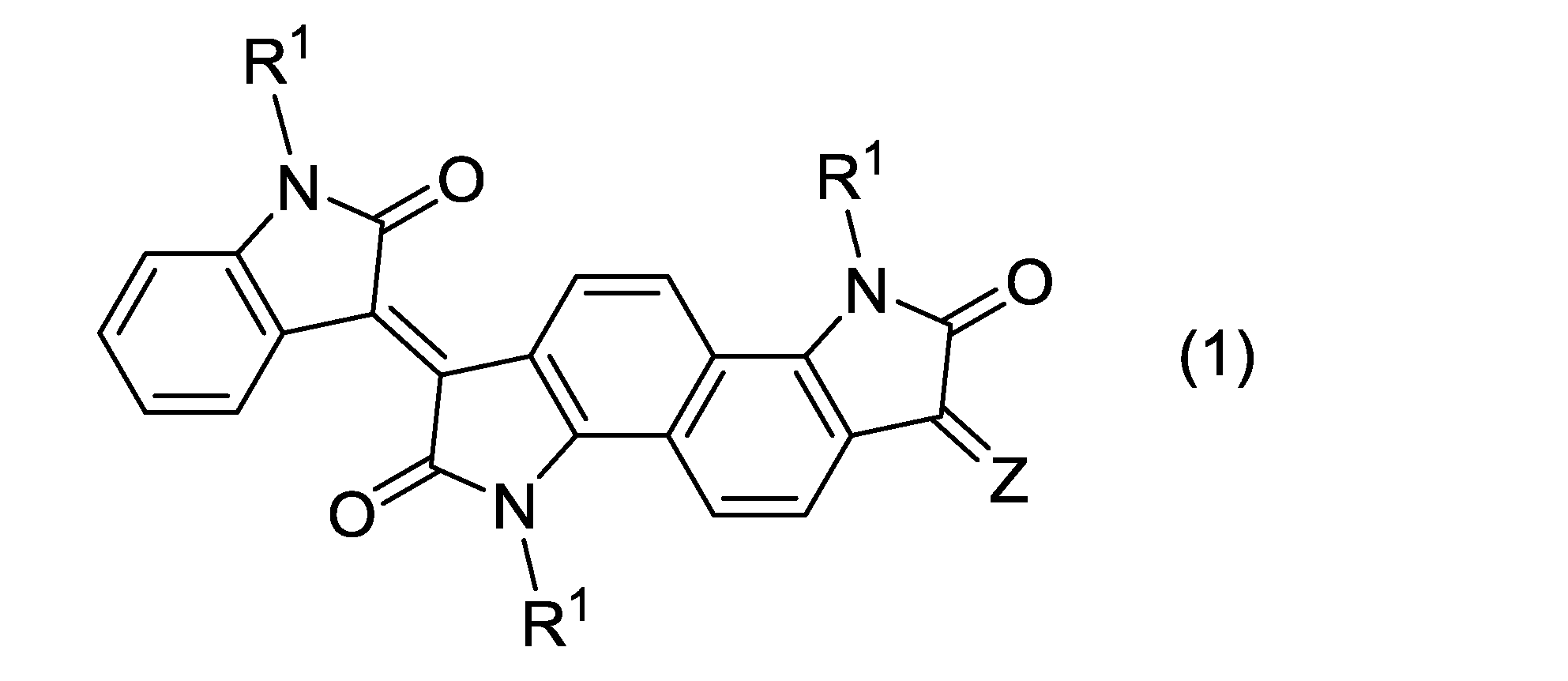
一般式(1)中、Zは、下記化学式(Z1)で表される基、又は下記一般式(Z2)で表される基を表す。

一般式(1)中のR1、及び一般式(Z2)中のR1は、炭素原子数1以上10以下のアルキル基で置換されてもよい炭素原子数6以上22以下のアリール基;炭素原子数7以上20以下のアラルキル基;炭素原子数3以上20以下のシクロアルキル基;炭素原子数1以上6以下のアルコキシ基;又は-CO-OR2基で置換されてもよい炭素原子数3以上30以下のアルキル基を表す。-CO-OR2基においてR2は、炭素原子数1以上8以下のアルキル基を表す。
感光層が化合物(1)を含有することで、感光体の感度特性を向上させることができる。その理由は、以下のように推測される。化合物(1)は、電子受容性基である4個のカルボニル基を含む所定の化学構造を有する。このため、化合物(1)は、電子受容性及び電子輸送性に優れる。また、一般式(1)において、1個の四環縮合環と、1個又は2個の二環縮合環とが、二重結合を介して結合されている。このため、化合物(1)は、広い平面構造を有する。化合物(1)が広い平面構造を有することから、電荷発生剤と化合物(1)との重なりが大きくなり、電荷発生剤から化合物(1)への電子受容性が向上する。また、化合物(1)が広い平面構造を有することから、化合物(1)の分子内における電子の移動距離が長くなり、電子輸送性が向上する。また、化合物(1)が広い平面構造を有することから、化合物(1)同士の重なりが大きくなり、化合物(1)の分子間における電子輸送性が向上する。これらのように電子受容性及び電子輸送性が向上することから、感光体の感度特性が向上する。
化学式(Z1)及び一般式(Z2)中、*は、一般式(1)中のZが結合している炭素原子に対する二重結合手を表す。一般式(1)中の3個のR1、及び一般式(Z2)中の1個のR1は、互いに同一の基を表す。
一般式(1)中のR1、及び一般式(Z2)中のR1が表わす炭素原子数6以上22以下のアリール基としては、炭素原子数6以上10以下のアリール基が好ましく、フェニル基がより好ましい。
一般式(1)中のR1、及び一般式(Z2)中のR1が表わす炭素原子数6以上22以下のアリール基は、炭素原子数1以上10以下のアルキル基で置換されてもよい。炭素原子数6以上22以下のアリール基の置換基である炭素原子数1以上10以下のアルキル基としては、炭素原子数1以上6以下のアルキル基が好ましく、炭素原子数1以上3以下のアルキル基がより好ましく、メチル基及びエチル基が更に好ましい。炭素原子数6以上22以下のアリール基が有する置換基(即ち、炭素原子数1以上10以下のアルキル基)の数は、1個以上5個以下であることが好ましく、1個又は2個であることがより好ましく、2個であることが更に好ましい。炭素原子数6以上22以下のアリール基が炭素原子数1以上10以下のアルキル基で置換される場合、炭素原子数1以上10以下のアルキル基で置換された炭素原子数6以上22以下のアリール基としては、炭素原子数1以上6以下のアルキル基で置換された炭素原子数6以上10以下のアリール基が好ましく、炭素原子数1以上3以下のアルキル基で置換されたフェニル基がより好ましく、エチルメチルフェニル基が更に好ましく、2-エチル-6-メチルフェニル基が特に好ましい。
一般式(1)中のR1、及び一般式(Z2)中のR1が表わす炭素原子数7以上20以下のアラルキル基としては、炭素原子数6以上14以下のアリール基で置換された炭素原子数1以上6以下のアルキル基が好ましく、フェニル基で置換された炭素原子数1以上3以下のアルキル基がより好ましく、ベンジル基が更に好ましい。
一般式(1)中のR1、及び一般式(Z2)中のR1が表わす炭素原子数3以上20以下のシクロアルキル基としては、炭素原子数3以上10以下のシクロアルキル基が好ましい。
一般式(1)中のR1、及び一般式(Z2)中のR1が表わす炭素原子数1以上6以下のアルコキシ基としては、炭素原子数1以上3以下のアルコキシ基が好ましい。
一般式(1)中のR1、及び一般式(Z2)中のR1が表わす炭素原子数3以上30以下のアルキル基としては、炭素原子数3以上15以下のアルキル基が好ましく、炭素原子数5以上12以下のアルキル基がより好ましく、炭素原子数5又は12のアルキル基が一層好ましく、2-ブチルオクチル基又は3-メチルブチル基が特に好ましい。
一般式(1)中のR1、及び一般式(Z2)中のR1が表わす炭素原子数3以上30以下のアルキル基は、-CO-OR2基で置換されてもよい。-CO-OR2基において、R2は、炭素原子数1以上8以下のアルキル基を表す。R2が表わす炭素原子数1以上8以下のアルキル基としては、炭素原子数1以上3以下のアルキル基が好ましく、エチル基がより好ましい。R1が表わす炭素原子数3以上30以下のアルキル基が有する置換基(即ち、-CO-OR2基)の数は、1個以上5個以下であることが好ましく、1個以上3個以下であることがより好ましく、1個であることが更に好ましい。炭素原子数3以上30以下のアルキル基が-CO-OR2基で置換される場合、-CO-OR2基で置換された炭素原子数3以上30以下のアルキル基としては、-CO-OR2基(好ましくはR2が炭素原子数1以上3以下のアルキル基を表す-CO-OR2基、より好ましくはエトキシカルボニル基)で置換された炭素原子数5以上12以下のアルキル基が好ましく、エトキシカルボニル基で置換された炭素原子数5のアルキル基がより好ましく、1-エトキシカルボニル-3-メチルブチル基が更に好ましい。
感光体の感度特性を向上させるためには、一般式(1)中のR1、及び一般式(Z2)中のR1は、炭素原子数1以上10以下のアルキル基で置換されてもよい炭素原子数6以上22以下のアリール基;炭素原子数7以上20以下のアラルキル基;又は-CO-OR2基で置換されてもよい炭素原子数3以上30以下のアルキル基を表すことが好ましい。R2は、炭素原子数1以上8以下のアルキル基を表すことが好ましい。
感光体の感度特性を更に向上させるためには、一般式(1)中のR1、及び一般式(Z2)中のR1は、-CO-OR2基で置換されてもよい炭素原子数3以上30以下のアルキル基を表すことが好ましい。R2は、炭素原子数1以上8以下のアルキル基を表すことが好ましい。R1が炭素原子数3以上30以下のアルキル基のような長鎖アルキル基であることで、バインダー樹脂の主鎖に対して化合物(1)が有する長鎖アルキル基が絡み、バインダー樹脂と化合物(1)との相溶性が向上すると考えられる。このため、化合物(1)が感光層中に均一に分散して、感光体の感度特性が更に向上する。
一般式(1)中のZが化学式(Z1)で表される基である場合、一般式(1)は、一般式(1-Z1)で表される。一般式(1)中のZが一般式(Z2)で表される基である場合、一般式(1)は、一般式(1-Z2)で表される。一般式(1-Z1)及び(1-Z2)中のR1は、一般式(1)中のR1と同義である。
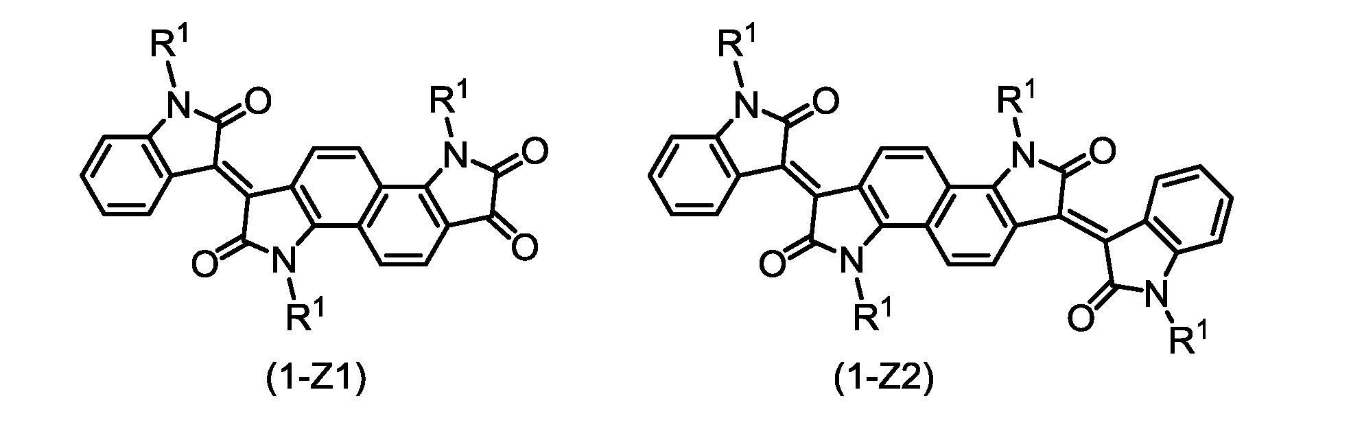
一般式(1)中のZが化学式(Z1)で表される基である場合、化合物(1)の好適な例としては、化学式(1-1)、(1-2)、(1-3)、及び(1-4)で表される化合物(以下、それぞれを化合物(1-1)、(1-2)、(1-3)、及び(1-4)と記載することがある)が挙げられる。感光体の感度特性を更に向上させるためには、化合物(1)としては、化合物(1-5)が特に好ましい。

一般式(1)中のZが一般式(Z2)で表される基である場合、化合物(1)の好適な例としては、化学式(1-5)、(1-6)、(1-7)、及び(1-8)で表される化合物(以下、それぞれを化合物(1-5)、(1-6)、(1-7)、及び(1-8)と記載することがある)が挙げられる。
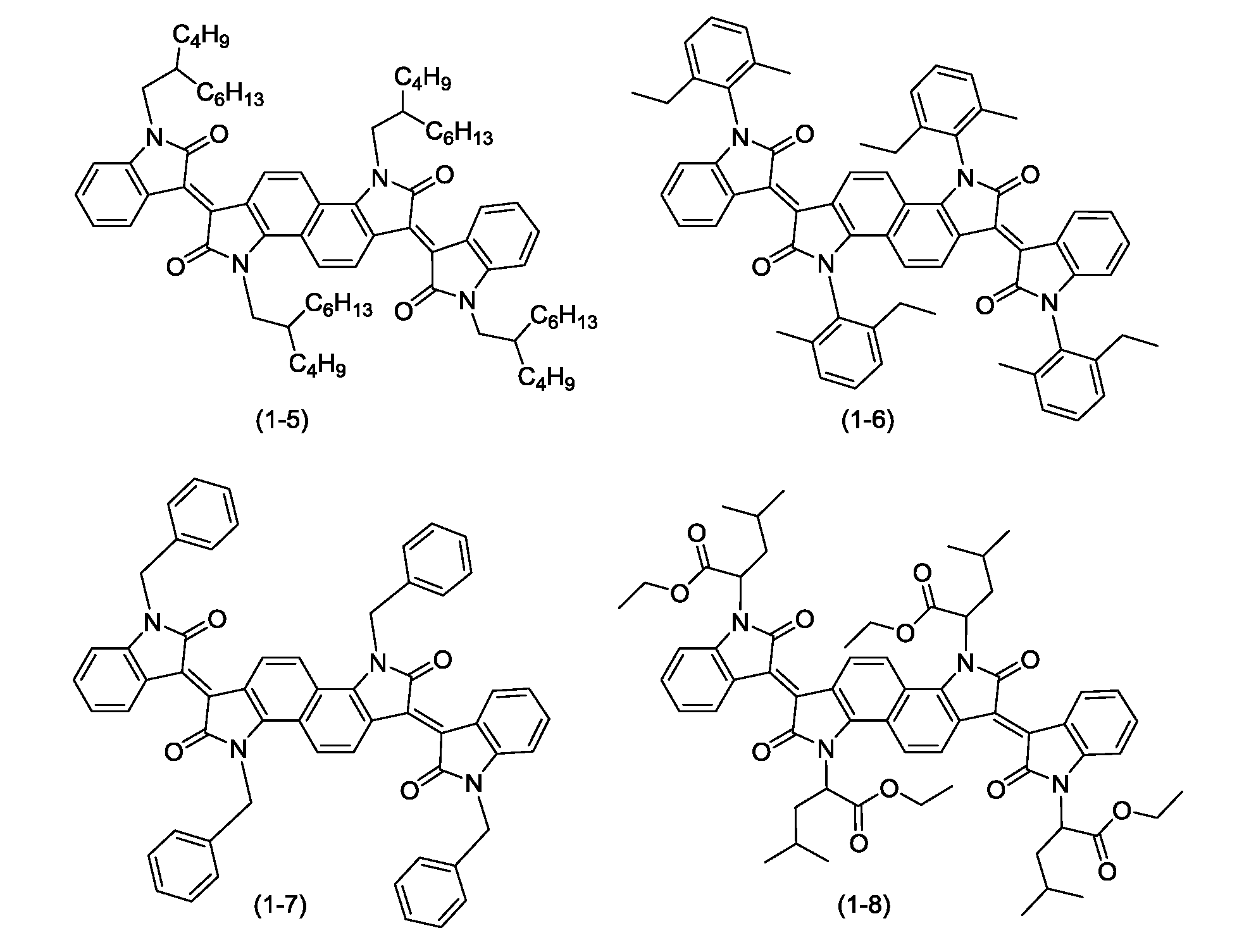
感光層は、1種の化合物(1)のみを含有してもよく、2種以上の化合物(1)を含有してもよい。また、感光層は、電子輸送剤として化合物(1)のみを含有してもよく、化合物(1)に加えて化合物(1)以外の電子輸送剤(以下、その他の電子輸送剤と記載することがある)を更に含有してもよい。その他の電子輸送剤の例としては、キノン化合物、ジイミド系化合物、ヒドラゾン系化合物、チオピラン系化合物、トリニトロチオキサントン系化合物、3,4,5,7-テトラニトロ-9-フルオレノン系化合物、ジニトロアントラセン系化合物、ジニトロアクリジン系化合物、テトラシアノエチレン、2,4,8-トリニトロチオキサントン、ジニトロベンゼン、ジニトロアクリジン、無水コハク酸、無水マレイン酸、及びジブロモ無水マレイン酸が挙げられる。キノン化合物としては、例えば、ジフェノキノン化合物、アゾキノン化合物、アントラキノン化合物、ナフトキノン化合物、ニトロアントラキノン化合物、及びジニトロアントラキノン化合物が挙げられる。
化合物(1)の含有量は、100質量部のバインダー樹脂に対して、5質量部以上100質量部以下であることが好ましく、20質量部以上40質量部以下であることがより好ましい。化合物(1)の含有量が100質量部のバインダー樹脂に対して5質量部以上であると、感光体の感度特性を向上させ易い。化合物(1)の含有量が100質量部のバインダー樹脂に対して100質量部以下であると、感光層形成用の溶剤に化合物(1)が溶解し易く、均一な感光層を形成し易い。
化合物(1)は、例えば、下記反応式(R-1)で表される反応(以下、反応(R-1)と記載することがある)に従って、又はこれに準ずる方法によって製造される。以下、反応式(R-1)で示す一般式(A)及び(B)で表される化合物を、各々、化合物(A)及び(B)と記載する。一般式(A)及び(B)中のR1は、一般式(1)及び一般式(Z2)中のR1と同義である。

まず、Zが化学式(Z1)で表される基である化合物(1)を製造する場合について説明する。Zが化学式(Z1)で表される基である化合物(1)を製造する場合、反応(R-1)では、1モル当量の化合物(A)と、1モル当量の化合物(B)とを反応させて、1モル当量の化合物(1)を得る。詳しくは、1モル当量の化合物(A)と、1モル当量の化合物(B)とを、酸触媒の存在下、溶媒中で攪拌する。酸触媒の例としては、パラトルエンスルホン酸が挙げられる。溶媒の例としては、n-ブチル酸、酢酸、及びプロピオン酸が挙げられる。反応(R-1)は、不活性ガス雰囲気下で行われてもよい。不活性ガスの例としては、窒素ガス、及びアルゴンガスが挙げられる。反応(R-1)の反応温度は、50℃以上180℃以下であることが好ましい。反応(R-1)の反応時間は、5時間以上20時間以下であることが好ましい。以上、Zが化学式(Z1)で表される基である化合物(1)を製造する場合について説明した。
次に、Zが一般式(Z2)で表される基である化合物(1)を製造する場合について説明する。Zが一般式(Z2)で表される基である化合物(1)を製造する場合、反応(R-1)では、1モル当量の化合物(A)と、2モル当量の化合物(B)とを反応させて、1モル当量の化合物(1)を得る。詳しくは、1モル当量の化合物(A)と、2モル当量の化合物(B)とを、酸触媒の存在下、溶媒中で攪拌する。反応(R-1)は、不活性ガス雰囲気下で行われてもよい。酸触媒の例、溶媒の例、不活性ガスの例、及び反応温度の好適な範囲は、Zが化学式(Z1)で表される基である化合物(1)を製造する場合と同じである。反応(R-1)の反応時間は、10時間以上30時間以下であることが好ましい。反応(R-1)において、脱水剤を更に添加してもよい。脱水剤の例としては、五酸化二リンが挙げられる。以上、Zが一般式(Z2)で表される基である化合物(1)を製造する場合について説明した。
なお、反応(R-1)で用いられる化合物(A)は、例えば、下記反応式(R-0)で表される反応(以下、反応(R-0)と記載することがある)に従って、又はこれに準ずる方法によって製造される。以下、反応式(R-0)で示す化学式(C)及び一般式(D)で表される化合物を、各々、化合物(C)及び(D)と記載する。一般式(D)中のR1は、一般式(1)及び一般式(Z2)中のR1と同義である。

反応(R-0)では、1モル当量の化合物(C)と、2モル当量の化合物(D)とを反応させて、1モル当量の化合物(A)を得る。詳しくは、化合物(C)と化合物(D)とを、塩基の存在下、溶媒中で攪拌する。塩基の例としては、炭酸カリウム、炭酸ナトリウム、及びリン酸カリウムが挙げられる。溶媒の例としては、N,N-ジメチルホルムアミド、及びテトラヒドロフランが挙げられる。反応(R-0)は、不活性ガス雰囲気下で行われることが好ましい。不活性ガスの例としては、窒素ガス、及びアルゴンガスが挙げられる。反応(R-0)の反応温度は、50℃以上150℃以下であることが好ましい。反応(R-0)の反応時間は、0.5時間以上5時間以下であることが好ましい。
(電荷発生剤)
電荷発生剤は、感光体用の電荷発生剤である限り、特に限定されない。電荷発生剤としては、例えば、フタロシアニン系顔料、ペリレン系顔料、ビスアゾ顔料、トリスアゾ顔料、ジチオケトピロロピロール顔料、無金属ナフタロシアニン顔料、金属ナフタロシアニン顔料、スクアライン顔料、インジゴ顔料、アズレニウム顔料、シアニン顔料、無機光導電材料(例えば、セレン、セレン-テルル、セレン-ヒ素、硫化カドミウム又はアモルファスシリコン)の粉末、ピリリウム顔料、アンサンスロン系顔料、トリフェニルメタン系顔料、スレン系顔料、トルイジン系顔料、ピラゾリン系顔料、及びキナクリドン系顔料が挙げられる。感光層は、1種の電荷発生剤のみを含有してもよく、2種以上の電荷発生剤を含有してもよい。
電荷発生剤は、感光体用の電荷発生剤である限り、特に限定されない。電荷発生剤としては、例えば、フタロシアニン系顔料、ペリレン系顔料、ビスアゾ顔料、トリスアゾ顔料、ジチオケトピロロピロール顔料、無金属ナフタロシアニン顔料、金属ナフタロシアニン顔料、スクアライン顔料、インジゴ顔料、アズレニウム顔料、シアニン顔料、無機光導電材料(例えば、セレン、セレン-テルル、セレン-ヒ素、硫化カドミウム又はアモルファスシリコン)の粉末、ピリリウム顔料、アンサンスロン系顔料、トリフェニルメタン系顔料、スレン系顔料、トルイジン系顔料、ピラゾリン系顔料、及びキナクリドン系顔料が挙げられる。感光層は、1種の電荷発生剤のみを含有してもよく、2種以上の電荷発生剤を含有してもよい。
フタロシアニン系顔料としては、例えば、無金属フタロシアニン、及び金属フタロシアニンが挙げられる。無金属フタロシアニンは、化学式(CGM2)で表される。金属フタロシアニンとしては、例えば、チタニルフタロシアニン、ヒドロキシガリウムフタロシアニン、及びクロロガリウムフタロシアニンが挙げられる。チタニルフタロシアニンは、化学式(CGM1)で表される。フタロシアニン系顔料は、結晶であってもよく、非結晶であってもよい。フタロシアニン系顔料の結晶形状(例えば、α型、β型、Y型、V型、又はII型)については特に限定されず、種々の結晶形状を有するフタロシアニン系顔料を使用できる。


無金属フタロシアニンの結晶としては、例えば、無金属フタロシアニンのX型結晶(以下、X型無金属フタロシアニンと記載することがある)が挙げられる。チタニルフタロシアニンの結晶としては、例えば、チタニルフタロシアニンのα型、β型、及びY型結晶(以下、α型、β型、及びY型チタニルフタロシアニンと記載することがある)が挙げられる。
例えば、デジタル光学式の画像形成装置(例えば、半導体レーザーのような光源を使用した、レーザービームプリンター又はファクシミリ)には、700nm以上の波長領域に感度を有する感光体を用いることが好ましい。700nm以上の波長領域で高い量子収率を有することから、電荷発生剤としては、フタロシアニン系顔料が好ましく、無金属フタロシアニン又はチタニルフタロシアニンがより好ましく、X型無金属フタロシアニン又はY型チタニルフタロシアニンが更に好ましく、Y型チタニルフタロシアニンが特に好ましい。
Y型チタニルフタロシアニンは、CuKα特性X線回折スペクトルにおいて、例えば、ブラッグ角(2θ±0.2°)の27.2°に主ピークを有する。CuKα特性X線回折スペクトルにおける主ピークとは、ブラッグ角(2θ±0.2°)が3°以上40°以下である範囲において、1番目又は2番目に大きな強度を有するピークである。
CuKα特性X線回折スペクトルの測定方法の一例について説明する。試料(チタニルフタロシアニン)をX線回折装置(例えば、株式会社リガク製「RINT(登録商標)1100」)のサンプルホルダーに充填して、X線管球Cu、管電圧40kV、管電流30mA、かつCuKα特性X線の波長1.542Åの条件で、X線回折スペクトルを測定する。測定範囲(2θ)は、例えば3°以上40°以下(スタート角3°、ストップ角40°)であり、走査速度は、例えば10°/分である。
短波長レーザー光源(例えば、350nm以上550nm以下の波長を有するレーザー光源)を用いた画像形成装置に適用される感光体には、電荷発生剤として、アンサンスロン系顔料が好適に用いられる。
電荷発生剤の含有量は、バインダー樹脂100質量部に対して、0.1質量部以上50質量部以下であることが好ましく、0.5質量部以上30質量部以下であることがより好ましく、0.5質量部以上4.5質量部以下であることが特に好ましい。
(正孔輸送剤)
正孔輸送剤としては、例えば、トリフェニルアミン誘導体、ジアミン誘導体(例えば、N,N,N’,N’-テトラフェニルベンジジン誘導体、N,N,N’,N’-テトラフェニルフェニレンジアミン誘導体、N,N,N’,N’-テトラフェニルナフチレンジアミン誘導体、N,N,N’,N’-テトラフェニルフェナントリレンジアミン誘導体、及びジ(アミノフェニルエテニル)ベンゼン誘導体)、オキサジアゾール系化合物(例えば、2,5-ジ(4-メチルアミノフェニル)-1,3,4-オキサジアゾール)、スチリル系化合物(例えば、9-(4-ジエチルアミノスチリル)アントラセン)、カルバゾール系化合物(例えば、ポリビニルカルバゾール)、有機ポリシラン化合物、ピラゾリン系化合物(例えば、1-フェニル-3-(p-ジメチルアミノフェニル)ピラゾリン)、ヒドラゾン系化合物、インドール系化合物、オキサゾール系化合物、イソオキサゾール系化合物、チアゾール系化合物、チアジアゾール系化合物、イミダゾール系化合物、ピラゾール系化合物、及びトリアゾール系化合物が挙げられる。感光層は、1種の正孔輸送剤のみを含有してもよく、2種以上の正孔輸送剤を含有してもよい。
正孔輸送剤としては、例えば、トリフェニルアミン誘導体、ジアミン誘導体(例えば、N,N,N’,N’-テトラフェニルベンジジン誘導体、N,N,N’,N’-テトラフェニルフェニレンジアミン誘導体、N,N,N’,N’-テトラフェニルナフチレンジアミン誘導体、N,N,N’,N’-テトラフェニルフェナントリレンジアミン誘導体、及びジ(アミノフェニルエテニル)ベンゼン誘導体)、オキサジアゾール系化合物(例えば、2,5-ジ(4-メチルアミノフェニル)-1,3,4-オキサジアゾール)、スチリル系化合物(例えば、9-(4-ジエチルアミノスチリル)アントラセン)、カルバゾール系化合物(例えば、ポリビニルカルバゾール)、有機ポリシラン化合物、ピラゾリン系化合物(例えば、1-フェニル-3-(p-ジメチルアミノフェニル)ピラゾリン)、ヒドラゾン系化合物、インドール系化合物、オキサゾール系化合物、イソオキサゾール系化合物、チアゾール系化合物、チアジアゾール系化合物、イミダゾール系化合物、ピラゾール系化合物、及びトリアゾール系化合物が挙げられる。感光層は、1種の正孔輸送剤のみを含有してもよく、2種以上の正孔輸送剤を含有してもよい。
感光層は、一般式(10)で表される化合物(以下、化合物(10)と記載することがある)を含有することが好ましい。感光層は、例えば、正孔輸送剤として、化合物(10)を含有することが好ましい。
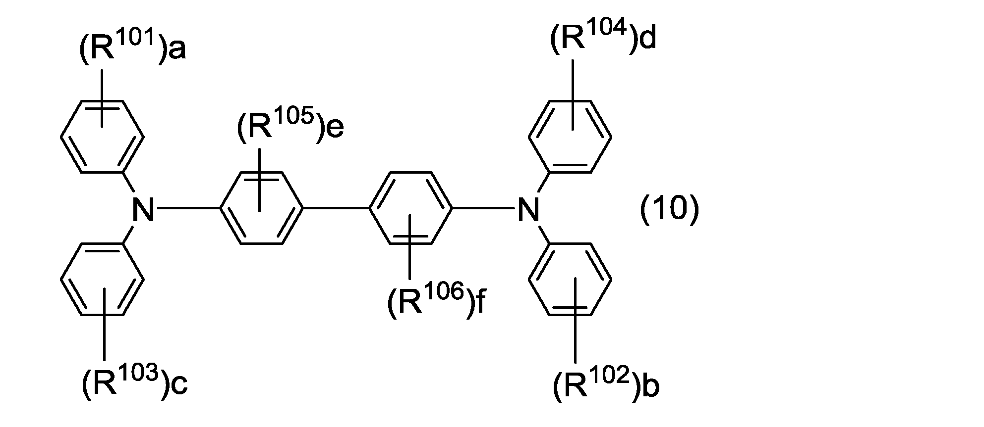
一般式(10)中、R101、R102、R103、R104、R105、及びR106は、各々独立に、炭素原子数1以上6以下のアルキル基、炭素原子数1以上6以下のアルコキシ基、又は炭素原子数6以上14以下のアリール基を表す。a、b、c、及びdは、各々独立に、0以上5以下の整数を表す。e、及びfは、各々独立に、0以上4以下の整数を表す。
aが2以上5以下の整数を表す場合、複数のR101は、互いに同一であっても異なっていてもよい。bが2以上5以下の整数を表す場合、複数のR102は、互いに同一であっても異なっていてもよい。cが2以上5以下の整数を表す場合、複数のR103は、互いに同一であっても異なっていてもよい。dが2以上5以下の整数を表す場合、複数のR104は、互いに同一であっても異なっていてもよい。eが2以上4以下の整数を表す場合、複数のR105は、互いに同一であっても異なっていてもよい。fが2以上4以下の整数を表す場合、複数のR106は、互いに同一であっても異なっていてもよい。
一般式(10)中、R101、R102、R103、R104、R105、及びR106は、各々独立に、炭素原子数1以上6以下のアルキル基を表すことが好ましく、炭素原子数1以上3以下のアルキル基を表すことがより好ましく、メチル基を表すことが更に好ましい。a、b、c及びdは、各々独立に、0又は1を表すことが好ましく、1を表すことがより好ましい。e及びfは、各々独立に、0又は1を表すことが好ましく、1を表すことがより好ましい。
化合物(10)の好適な例としては、下記化学式(10-1)で表される化合物(以下、化合物(10-1)と記載することがある)が挙げられる。

感光層は、正孔輸送剤として化合物(10)のみを含有してもよい。また、感光層は、正孔輸送剤として、化合物(10)に加えて、化合物(10)以外の正孔輸送剤を更に含有してもよい。
正孔輸送剤の含有量は、バインダー樹脂100質量部に対して、10質量部以上200質量部以下であることが好ましく、10質量部以上100質量部以下であることがより好ましい。
(バインダー樹脂)
バインダー樹脂としては、例えば、熱可塑性樹脂、熱硬化性樹脂、及び光硬化性樹脂が挙げられる。熱可塑性樹脂としては、例えば、ポリカーボネート樹脂、ポリアリレート樹脂、スチレン-ブタジエン共重合体、スチレン-アクリロニトリル共重合体、スチレン-マレイン酸共重合体、アクリル酸重合体、スチレン-アクリル酸共重合体、ポリエチレン樹脂、エチレン-酢酸ビニル共重合体、塩素化ポリエチレン樹脂、ポリ塩化ビニル樹脂、ポリプロピレン樹脂、アイオノマー樹脂、塩化ビニル-酢酸ビニル共重合体、アルキド樹脂、ポリアミド樹脂、ウレタン樹脂、ポリスルホン樹脂、ジアリルフタレート樹脂、ケトン樹脂、ポリビニルブチラール樹脂、ポリエステル樹脂、及びポリエーテル樹脂が挙げられる。熱硬化性樹脂としては、例えば、シリコーン樹脂、エポキシ樹脂、フェノール樹脂、尿素樹脂、及びメラミン樹脂が挙げられる。光硬化性樹脂としては、例えば、エポキシ化合物のアクリル酸付加物、及びウレタン化合物のアクリル酸付加物が挙げられる。感光層は、1種のバインダー樹脂のみを含有してもよく、2種以上のバインダー樹脂を含有してもよい。
バインダー樹脂としては、例えば、熱可塑性樹脂、熱硬化性樹脂、及び光硬化性樹脂が挙げられる。熱可塑性樹脂としては、例えば、ポリカーボネート樹脂、ポリアリレート樹脂、スチレン-ブタジエン共重合体、スチレン-アクリロニトリル共重合体、スチレン-マレイン酸共重合体、アクリル酸重合体、スチレン-アクリル酸共重合体、ポリエチレン樹脂、エチレン-酢酸ビニル共重合体、塩素化ポリエチレン樹脂、ポリ塩化ビニル樹脂、ポリプロピレン樹脂、アイオノマー樹脂、塩化ビニル-酢酸ビニル共重合体、アルキド樹脂、ポリアミド樹脂、ウレタン樹脂、ポリスルホン樹脂、ジアリルフタレート樹脂、ケトン樹脂、ポリビニルブチラール樹脂、ポリエステル樹脂、及びポリエーテル樹脂が挙げられる。熱硬化性樹脂としては、例えば、シリコーン樹脂、エポキシ樹脂、フェノール樹脂、尿素樹脂、及びメラミン樹脂が挙げられる。光硬化性樹脂としては、例えば、エポキシ化合物のアクリル酸付加物、及びウレタン化合物のアクリル酸付加物が挙げられる。感光層は、1種のバインダー樹脂のみを含有してもよく、2種以上のバインダー樹脂を含有してもよい。
これらの樹脂のうち、加工性、機械的特性、光学的特性、及び耐摩耗性のバランスに優れた感光層が得られることから、バインダー樹脂としては、ポリカーボネート樹脂が好ましい。ポリカーボネート樹脂の例としては、ビスフェノールZC型ポリカーボネート樹脂、ビスフェノールC型ポリカーボネート樹脂、ビスフェノールA型ポリカーボネート樹脂、及びビスフェノールZ型ポリカーボネート樹脂が挙げられる。ビスフェノールZ型ポリカーボネート樹脂は、下記化学式(20)で表される繰り返し単位を有する。以下、化学式(20)で表される繰り返し単位を有するポリカーボネート樹脂を、ポリカーボネート樹脂(20)と記載することがある。ポリカーボネート樹脂(20)は、繰返し単位として、繰り返し単位(20)のみを有することが好ましい。

(添加剤)
添加剤としては、例えば、劣化防止剤(例えば、酸化防止剤、ラジカル捕捉剤、1重項消光剤又は紫外線吸収剤)、軟化剤、表面改質剤、増量剤、増粘剤、分散安定剤、ワックス、アクセプター、ドナー、界面活性剤、可塑剤、増感剤、及びレベリング剤が挙げられる。
添加剤としては、例えば、劣化防止剤(例えば、酸化防止剤、ラジカル捕捉剤、1重項消光剤又は紫外線吸収剤)、軟化剤、表面改質剤、増量剤、増粘剤、分散安定剤、ワックス、アクセプター、ドナー、界面活性剤、可塑剤、増感剤、及びレベリング剤が挙げられる。
(材料の組み合わせ)
感光層に含有される材料は、以下に示す組み合わせの何れかであることが好ましい。組み合わせの一例において、電子輸送剤が化合物(1-1)、(1-2)、(1-3)、(1-4)、(1-5)、(1-6)、(1-7)、又は(1-8)を含み、正孔輸送剤が化合物(10-1)を含む。組み合わせの一例において、電子輸送剤が化合物(1-1)、(1-2)、(1-3)、(1-4)、(1-5)、(1-6)、(1-7)、又は(1-8)を含み、バインダーがポリカーボネート樹脂(20)を含む。組み合わせの一例において、電子輸送剤が化合物(1-1)、(1-2)、(1-3)、(1-4)、(1-5)、(1-6)、(1-7)、又は(1-8)を含み、電荷発生剤がX型無金属フタロシアニンを含む。組み合わせの一例において、電子輸送剤が化合物(1-1)、(1-2)、(1-3)、(1-4)、(1-5)、(1-6)、(1-7)、又は(1-8)を含み、電荷発生剤がY型チタニルフタロシアニンを含む。組み合わせの一例において、電子輸送剤が化合物(1-1)、(1-2)、(1-3)、(1-4)、(1-5)、(1-6)、(1-7)、又は(1-8)を含み、正孔輸送剤が化合物(10-1)を含み、バインダーがポリカーボネート樹脂(20)を含む。組み合わせの一例において、電子輸送剤が化合物(1-1)、(1-2)、(1-3)、(1-4)、(1-5)、(1-6)、(1-7)、又は(1-8)を含み、正孔輸送剤が化合物(10-1)を含み、バインダーがポリカーボネート樹脂(20)を含み、電荷発生剤がX型無金属フタロシアニンを含む。組み合わせの一例において、電子輸送剤が化合物(1-1)、(1-2)、(1-3)、(1-4)、(1-5)、(1-6)、(1-7)、又は(1-8)を含み、正孔輸送剤が化合物(10-1)を含み、バインダーがポリカーボネート樹脂(20)を含み、電荷発生剤がY型チタニルフタロシアニンを含む。
感光層に含有される材料は、以下に示す組み合わせの何れかであることが好ましい。組み合わせの一例において、電子輸送剤が化合物(1-1)、(1-2)、(1-3)、(1-4)、(1-5)、(1-6)、(1-7)、又は(1-8)を含み、正孔輸送剤が化合物(10-1)を含む。組み合わせの一例において、電子輸送剤が化合物(1-1)、(1-2)、(1-3)、(1-4)、(1-5)、(1-6)、(1-7)、又は(1-8)を含み、バインダーがポリカーボネート樹脂(20)を含む。組み合わせの一例において、電子輸送剤が化合物(1-1)、(1-2)、(1-3)、(1-4)、(1-5)、(1-6)、(1-7)、又は(1-8)を含み、電荷発生剤がX型無金属フタロシアニンを含む。組み合わせの一例において、電子輸送剤が化合物(1-1)、(1-2)、(1-3)、(1-4)、(1-5)、(1-6)、(1-7)、又は(1-8)を含み、電荷発生剤がY型チタニルフタロシアニンを含む。組み合わせの一例において、電子輸送剤が化合物(1-1)、(1-2)、(1-3)、(1-4)、(1-5)、(1-6)、(1-7)、又は(1-8)を含み、正孔輸送剤が化合物(10-1)を含み、バインダーがポリカーボネート樹脂(20)を含む。組み合わせの一例において、電子輸送剤が化合物(1-1)、(1-2)、(1-3)、(1-4)、(1-5)、(1-6)、(1-7)、又は(1-8)を含み、正孔輸送剤が化合物(10-1)を含み、バインダーがポリカーボネート樹脂(20)を含み、電荷発生剤がX型無金属フタロシアニンを含む。組み合わせの一例において、電子輸送剤が化合物(1-1)、(1-2)、(1-3)、(1-4)、(1-5)、(1-6)、(1-7)、又は(1-8)を含み、正孔輸送剤が化合物(10-1)を含み、バインダーがポリカーボネート樹脂(20)を含み、電荷発生剤がY型チタニルフタロシアニンを含む。
<導電性基体>
導電性基体は、少なくとも表面部が導電性を有する材料で形成されていればよい。導電性基体の一例としては、導電性を有する材料で構成される導電性基体が挙げられる。導電性基体の別の例としては、導電性を有する材料で被覆された導電性基体が挙げられる。導電性を有する材料としては、例えば、アルミニウム、鉄、銅、錫、白金、銀、バナジウム、モリブデン、クロム、カドミウム、チタン、ニッケル、パラジウム、インジウム、ステンレス鋼、及び真鍮が挙げられる。これらの導電性を有する材料の1種を単独で用いてもよいし、2種以上を組み合わせて(例えば、合金として)用いてもよい。これらの導電性を有する材料のなかでも、感光層から導電性基体への電荷の移動が良好であることから、アルミニウム、又はアルミニウム合金が好ましい。
導電性基体は、少なくとも表面部が導電性を有する材料で形成されていればよい。導電性基体の一例としては、導電性を有する材料で構成される導電性基体が挙げられる。導電性基体の別の例としては、導電性を有する材料で被覆された導電性基体が挙げられる。導電性を有する材料としては、例えば、アルミニウム、鉄、銅、錫、白金、銀、バナジウム、モリブデン、クロム、カドミウム、チタン、ニッケル、パラジウム、インジウム、ステンレス鋼、及び真鍮が挙げられる。これらの導電性を有する材料の1種を単独で用いてもよいし、2種以上を組み合わせて(例えば、合金として)用いてもよい。これらの導電性を有する材料のなかでも、感光層から導電性基体への電荷の移動が良好であることから、アルミニウム、又はアルミニウム合金が好ましい。
導電性基体の形状は、画像形成装置の構造に合わせて適宜選択される。導電性基体の形状としては、例えば、シート状、及びドラム状が挙げられる。また、導電性基体の厚さは、導電性基体の形状に応じて適宜選択される。
<中間層>
中間層(下引き層)は、例えば、無機粒子、及び中間層に用いられる樹脂(中間層用樹脂)を含有する。中間層が存在することにより、リーク発生を抑制し得る程度の絶縁状態を維持しつつ、感光体を露光した時に発生する電流の流れを円滑にして、抵抗の上昇が抑えられる。
中間層(下引き層)は、例えば、無機粒子、及び中間層に用いられる樹脂(中間層用樹脂)を含有する。中間層が存在することにより、リーク発生を抑制し得る程度の絶縁状態を維持しつつ、感光体を露光した時に発生する電流の流れを円滑にして、抵抗の上昇が抑えられる。
無機粒子としては、例えば、金属(例えば、アルミニウム、鉄、又は銅)の粒子、金属酸化物(例えば、酸化チタン、アルミナ、酸化ジルコニウム、酸化スズ、又は酸化亜鉛)の粒子、及び非金属酸化物(例えば、シリカ)の粒子が挙げられる。これらの無機粒子は、1種を単独で用いてもよいし、2種以上を併用してもよい。
中間層用樹脂の例は、感光層に含有されるバインダー樹脂の例と同じである。中間層は、必要に応じて、添加剤を含有してもよい。中間層に含有される添加剤の例は、感光層に含有される添加剤の例と同じである。
<感光体の製造方法>
感光体は、例えば、感光層形成用塗布液(以下、塗布液と記載することがある)を導電性基体上に塗布し、乾燥することによって製造される。塗布液は、電荷発生剤、化合物(1)、及び必要に応じて添加される成分(例えば、正孔輸送剤、バインダー樹脂、及び添加剤)を、溶剤に溶解又は分散させることにより製造される。
感光体は、例えば、感光層形成用塗布液(以下、塗布液と記載することがある)を導電性基体上に塗布し、乾燥することによって製造される。塗布液は、電荷発生剤、化合物(1)、及び必要に応じて添加される成分(例えば、正孔輸送剤、バインダー樹脂、及び添加剤)を、溶剤に溶解又は分散させることにより製造される。
塗布液に含有される溶剤は、塗布液に含まれる各成分を溶解又は分散できる限り、特に限定されない。溶剤の例としては、アルコール類(例えば、メタノール、エタノール、イソプロパノール又はブタノール)、脂肪族炭化水素(例えば、n-ヘキサン、オクタン又はシクロヘキサン)、芳香族炭化水素(例えば、ベンゼン、トルエン又はキシレン)、ハロゲン化炭化水素(例えば、ジクロロメタン、ジクロロエタン、四塩化炭素又はクロロベンゼン)、エーテル類(例えば、ジメチルエーテル、ジエチルエーテル、テトラヒドロフラン、エチレングリコールジメチルエーテル、ジエチレングリコールジメチルエーテル又はプロピレングリコールモノメチルエーテル)、ケトン類(例えば、アセトン、メチルエチルケトン又はシクロヘキサノン)、エステル類(例えば、酢酸エチル又は酢酸メチル)、ジメチルホルムアルデヒド、ジメチルホルムアミド、及びジメチルスルホキシドが挙げられる。これらの溶剤の1種を単独で用いてもよく、2種以上を組み合わせて用いてもよい。感光体の製造時の作業性を向上させるためには、非ハロゲン溶剤(ハロゲン化炭化水素以外の溶剤)を用いることが好ましい。
塗布液は、各成分を混合し、溶剤に分散することにより調製される。混合又は分散には、例えば、ビーズミル、ロールミル、ボールミル、アトライター、ペイントシェーカー、又は超音波分散機を用いることができる。
塗布液は、各成分の分散性を向上させるために、例えば、界面活性剤を含有してもよい。
塗布液を塗布する方法としては、塗布液を導電性基体上に均一に塗布できる方法である限り、特に限定されない。塗布方法としては、例えば、ブレードコート法、ディップコート法、スプレーコート法、スピンコート法、及びバーコート法が挙げられる。
塗布液を乾燥する方法としては、塗布液中の溶剤を蒸発させ得る限り、特に限定されない。例えば、高温乾燥機又は減圧乾燥機を用いて、熱処理(熱風乾燥)する方法が挙げられる。熱処理温度は、例えば、40℃以上150℃以下の温度である。熱処理時間は、例えば、3分間以上120分間以下である。
なお、感光体の製造方法は、必要に応じて、中間層を形成する工程及び保護層を形成する工程の一方又は両方を更に含んでもよい。中間層を形成する工程及び保護層を形成する工程では、公知の方法が適宜選択される。
以下、実施例を用いて本発明を更に具体的に説明する。ただし、本発明は実施例の範囲に何ら限定されない。
<感光層を形成するための材料>
感光体の感光層を形成するための材料として、以下の電荷発生剤、正孔輸送剤、バインダー樹脂、及び電子輸送剤を準備した。
感光体の感光層を形成するための材料として、以下の電荷発生剤、正孔輸送剤、バインダー樹脂、及び電子輸送剤を準備した。
(電荷発生剤)
電荷発生剤として、Y型チタニルフタロシアニン及びX型無金属フタロシアニンを準備した。Y型チタニルフタロシアニンは、実施形態で述べた化学式(CGM1)で表され、Y型の結晶構造を有するチタニルフタロシアニンであった。X型無金属フタロシアニンは、実施形態で述べた化学式(CGM2)で表され、X型の結晶構造を有する無金属フタロシアニンであった。
電荷発生剤として、Y型チタニルフタロシアニン及びX型無金属フタロシアニンを準備した。Y型チタニルフタロシアニンは、実施形態で述べた化学式(CGM1)で表され、Y型の結晶構造を有するチタニルフタロシアニンであった。X型無金属フタロシアニンは、実施形態で述べた化学式(CGM2)で表され、X型の結晶構造を有する無金属フタロシアニンであった。
(正孔輸送剤)
正孔輸送剤として、実施形態で述べた化合物(10-1)を準備した。
正孔輸送剤として、実施形態で述べた化合物(10-1)を準備した。
(バインダー樹脂)
バインダー樹脂として、実施形態で述べたポリカーボネート樹脂(20)を準備した。ポリカーボネート樹脂(20)の粘度平均分子量は、50000であった。
バインダー樹脂として、実施形態で述べたポリカーボネート樹脂(20)を準備した。ポリカーボネート樹脂(20)の粘度平均分子量は、50000であった。
(電子輸送剤)
電子輸送剤として、実施形態で述べた化合物(1-1)~(1-8)の各々を、以下の方法で合成した。各化合物の収率は、モル比換算により求めた。
電子輸送剤として、実施形態で述べた化合物(1-1)~(1-8)の各々を、以下の方法で合成した。各化合物の収率は、モル比換算により求めた。
(化合物(1-1)の合成)
下記反応式(r-1a)で表される反応(以下、反応(r-1a)と記載する)に従って、化合物(1-1)を合成した。なお、以下で述べる化合物(A-1)~(A-4)、及び(B-1)~(B-4)は、各々、反応式(r-1a)中の化学式(A-1)及び(B-1)、並びに後述する化学式(A-2)~(A-4)及び(B-1)~(B-4)で表される。
下記反応式(r-1a)で表される反応(以下、反応(r-1a)と記載する)に従って、化合物(1-1)を合成した。なお、以下で述べる化合物(A-1)~(A-4)、及び(B-1)~(B-4)は、各々、反応式(r-1a)中の化学式(A-1)及び(B-1)、並びに後述する化学式(A-2)~(A-4)及び(B-1)~(B-4)で表される。

反応(r-1a)では、約1モル当量の化合物(A-1)と、約1モル当量の化合物(B-1)とを反応させて、化合物(1-1)を得た。詳しくは、化合物(A-1)(0.656g、1.09mmol)と、パラトルエンスルホン酸1水和物(38mg、0.199mmol)とを、n-ブチル酸(10mL)に溶解させて、溶液を得た。溶液を130℃に加熱した後、溶液に化合物(B-1)(0.287g、0.955mmol)を滴下した。滴下後、溶液を130℃で16時間攪拌した。次いで、溶液を室温に冷却した。次いで、溶液に水(40mL)を加えて、析出した固体を濾過により取り出した。濾紙上の固体を、水で洗浄し、次いでエタノールで洗浄した。展開溶媒としてクロロホルムを用いて、シリカゲルカラムクロマトグラフィーにより、洗浄後の濾紙上の固体を精製して、化合物(1-1)を得た。化合物(1-1)の収量は、0.497gであった。化合物(A-1)からの化合物(1-1)の収率は、56%であった。
(化合物(1-2)~(1-4)の合成)
次の点を変更した以外は、化合物(1-1)の合成と同じ方法で、化合物(1-2)~(1-4)の各々を合成した。化合物(1-1)の合成では化合物(A-1)(0.656g、1.09mmol)を添加したが、化合物(1-2)~(1-4)の各々の合成では、表1の化合物(A)欄に示す質量及び種類の化合物を添加した。化合物(1-1)の合成では化合物(B-1)(0.287g、0.955mmol)を添加したが、化合物(1-2)~(1-4)の各々の合成では、表1の化合物(B)欄に示す質量及び種類の化合物を添加した。なお、表1の化合物(A)欄に示す化合物の添加量は何れも1.09mmolであり、化合物(B)欄に示す化合物の添加量は何れも0.955mmolであった。また、化合物(A)欄に示す化合物からの化合物(1-1)~(1-4)の収量及び収率を、表1に示す。
次の点を変更した以外は、化合物(1-1)の合成と同じ方法で、化合物(1-2)~(1-4)の各々を合成した。化合物(1-1)の合成では化合物(A-1)(0.656g、1.09mmol)を添加したが、化合物(1-2)~(1-4)の各々の合成では、表1の化合物(A)欄に示す質量及び種類の化合物を添加した。化合物(1-1)の合成では化合物(B-1)(0.287g、0.955mmol)を添加したが、化合物(1-2)~(1-4)の各々の合成では、表1の化合物(B)欄に示す質量及び種類の化合物を添加した。なお、表1の化合物(A)欄に示す化合物の添加量は何れも1.09mmolであり、化合物(B)欄に示す化合物の添加量は何れも0.955mmolであった。また、化合物(A)欄に示す化合物からの化合物(1-1)~(1-4)の収量及び収率を、表1に示す。
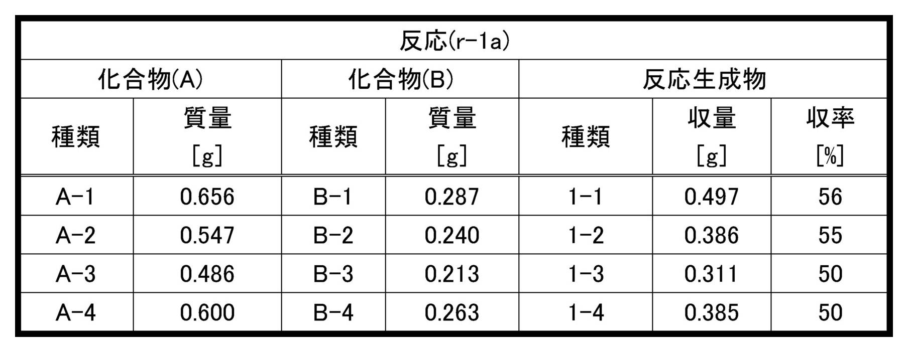
なお、化合物(A-2)~(A-4)及び(B-2)~(B-4)は、各々、下記化学式(A-2)~(A-4)及び(B-2)~(B-4)で表される。

(化合物(1-5)の合成)
下記反応式(r-1b)で表される反応(以下、反応(r-1b)と記載する)に従って、化合物(1-5)を合成した。
下記反応式(r-1b)で表される反応(以下、反応(r-1b)と記載する)に従って、化合物(1-5)を合成した。
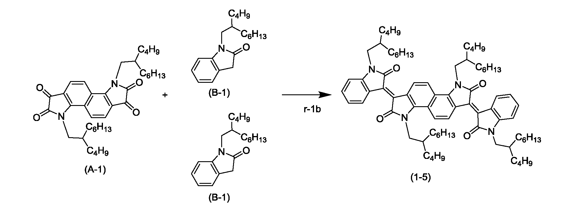
反応(r-1b)では、約1モル当量の化合物(A-1)と、約2モル当量の化合物(B-1)とを反応させて、化合物(1-5)を得た。詳しくは、化合物(A-1)(0.250g、0.415mmol)と、パラトルエンスルホン酸1水和物(28mg、0.145mmol)と、五酸化二リン(41mg、0.290mmol)と、化合物(B-1)(0.262g、0.871mmol)とを、酢酸(15mL)に溶解させて、溶液を得た。溶液を、窒素ガス雰囲気下、125℃で24時間攪拌した。次いで、溶液を室温に冷却した。次いで、溶液に水(40mL)を加えて、析出した固体を濾過により取り出した。濾紙上の固体を、水で洗浄し、次いでエタノールで洗浄した。展開溶媒としてクロロホルムを用いて、シリカゲルカラムクロマトグラフィーにより、洗浄後の濾紙上の固体を精製して、化合物(1-5)を得た。化合物(1-5)の収量は、0.296gであった。化合物(A-1)からの化合物(1-5)の収率は、61%であった。
(化合物(1-6)~(1-8)の合成)
次の点を変更した以外は、化合物(1-5)の合成と同じ方法で、化合物(1-6)~(1-8)の各々を合成した。化合物(1-5)の合成では化合物(A-1)(0.250g、0.415mmol)を添加したが、化合物(1-6)~(1-8)の各々の合成では、表2の化合物(A)欄に示す質量及び種類の化合物を添加した。化合物(1-5)の合成では化合物(B-1)(0.262g、0.871mmol)を添加したが、化合物(1-6)~(1-8)の各々の合成では、表2の化合物(B)欄に示す質量及び種類の化合物を添加した。なお、表1の化合物(A)欄に示す化合物の添加量は何れも0.415mmolであり、化合物(B)欄に示す化合物の添加量は何れも0.871mmolであった。また、化合物(A)欄に示す化合物からの化合物(1-5)~(1-8)の収量及び収率を、表2に示す。
次の点を変更した以外は、化合物(1-5)の合成と同じ方法で、化合物(1-6)~(1-8)の各々を合成した。化合物(1-5)の合成では化合物(A-1)(0.250g、0.415mmol)を添加したが、化合物(1-6)~(1-8)の各々の合成では、表2の化合物(A)欄に示す質量及び種類の化合物を添加した。化合物(1-5)の合成では化合物(B-1)(0.262g、0.871mmol)を添加したが、化合物(1-6)~(1-8)の各々の合成では、表2の化合物(B)欄に示す質量及び種類の化合物を添加した。なお、表1の化合物(A)欄に示す化合物の添加量は何れも0.415mmolであり、化合物(B)欄に示す化合物の添加量は何れも0.871mmolであった。また、化合物(A)欄に示す化合物からの化合物(1-5)~(1-8)の収量及び収率を、表2に示す。

1H-NMR(プロトン核磁気共鳴分光計)を用いて、合成した化合物(1-1)~(1-8)の1H-NMRスペクトルを測定した。磁場強度を400MHzに設定した。溶媒として、重水素化クロロホルム(CDCl3)を使用した。内部標準物質としてテトラメチルシラン(TMS)を使用した。化合物(1-1)~(1-8)のうちの代表例として、化合物(1-1)及び(1-5)の1H-NMRスペクトルの化学シフト値を以下に示す。測定された1H-NMRスペクトルの化学シフト値から、化合物(1-1)及び(1-5)が得られていることを確認した。化合物(1-2)~(1-4)及び(1-6)~(1-8)についても、測定された1H-NMRスペクトルの化学シフト値から、化合物(1-2)~(1-5)が得られていることを確認した。
化合物(1-1):1H-NMR(400MHz,CDCl3,ppm) δ 9.11-9.13 (d, 1H), 9.07-9.09 (d, 1H), 7.95-7.97 (d, 1H), 7.84-7.87 (d, 1H), 7.52-7.54 (d, 1H), 7.37-7.41 (t, 1H), 7.04-7.07 (t, 1H), 6.78-6.79 (d, 1H), 4.25-4.26 (d, 2H), 4.15-4.16 (d, 2H), 3.66-3.68 (d, 2H), 1.98-2.10 (m, 1H), 1.83-1.98 (m, 2H), 1.09-1.48 (m, 48H), 0.75-0.98 (m, 18H).
化合物(1-5):1H-NMR(400MHz,CDCl3,ppm) δ 9.05-9.07 (d, 2H), 8.97-9.00 (d, 2H), 7.84-7.87 (d, 2H), 7.33-7.37 (t, 2H), 7.02-7.06 (t, 2H), 6.77-6.79 (d, 2H), 4.25-4.26 (d, 4H), 3.67-3.68 (d, 4H), 2.00-2.10 (m, 2H), 1.85-2.00 (m, 2H), 1.10-1.48 (m, 64H), 0.76-0.96 (m, 24H).
なお、比較例で使用する電子輸送剤として、下記化学式(E-1)で表される化合物(以下、化合物(E-1)と記載する)を準備した。
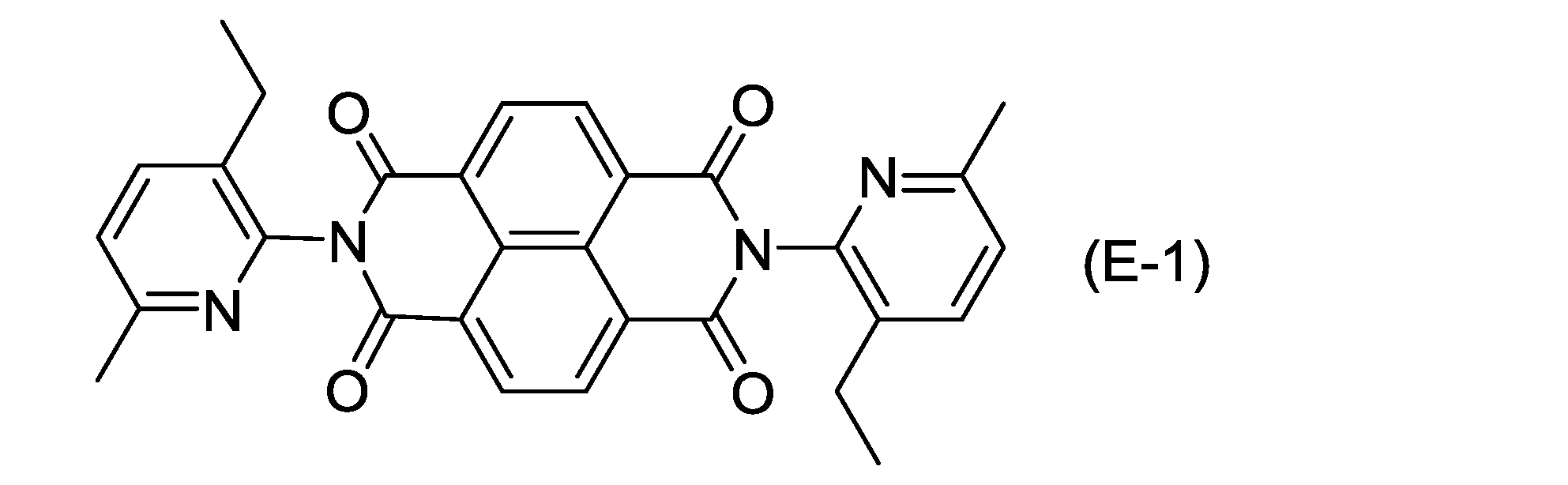
<感光体の製造>
感光層を形成するための材料を用いて、感光体(A-1)~(A-16)及び(B-1)~(B-2)の各々を製造した。
感光層を形成するための材料を用いて、感光体(A-1)~(A-16)及び(B-1)~(B-2)の各々を製造した。
(感光体(A-1)の製造)
電荷発生剤であるX型無金属フタロシアニン2質量部、正孔輸送剤である化合物(10-1)50質量部、電子輸送剤である化合物(1-1)30質量部、バインダー樹脂であるポリカーボネート樹脂(20)100質量部、及び溶剤であるテトラヒドロフラン600質量部を、ボールミルを用いて12時間混合して、塗布液を得た。塗布液を、導電性基体(アルミニウム製のドラム状支持体、直径30mm、全長238.5mm)上に、ブレードコート法を用いて塗布した。塗布した塗布液を、120℃で80分間熱風乾燥させた。このようにして、導電性基体上に単層の感光層(膜厚30μm)を形成し、感光体(A-1)を得た。
電荷発生剤であるX型無金属フタロシアニン2質量部、正孔輸送剤である化合物(10-1)50質量部、電子輸送剤である化合物(1-1)30質量部、バインダー樹脂であるポリカーボネート樹脂(20)100質量部、及び溶剤であるテトラヒドロフラン600質量部を、ボールミルを用いて12時間混合して、塗布液を得た。塗布液を、導電性基体(アルミニウム製のドラム状支持体、直径30mm、全長238.5mm)上に、ブレードコート法を用いて塗布した。塗布した塗布液を、120℃で80分間熱風乾燥させた。このようにして、導電性基体上に単層の感光層(膜厚30μm)を形成し、感光体(A-1)を得た。
(感光体(A-2)~(A-16)及び(B-1)~(B-2)の製造)
次の点を変更した以外は、感光体(A-1)の製造と同じ方法で、感光体(A-2)~(A-16)及び(B-1)~(B-2)の各々を製造した。感光体(A-1)の製造においては電荷発生剤としてX型無金属フタロシアニンを使用したが、感光体(A-2)~(A-16)及び(B-1)~(B-2)の各々の製造においては表3に示す種類の電荷発生剤を使用した。感光体(A-1)の製造においては電子輸送剤として化合物(1-1)を使用したが、感光体(A-2)~(A-16)及び(B-1)~(B-2)の各々の製造においては表3に示す種類の電子輸送剤を使用した。
次の点を変更した以外は、感光体(A-1)の製造と同じ方法で、感光体(A-2)~(A-16)及び(B-1)~(B-2)の各々を製造した。感光体(A-1)の製造においては電荷発生剤としてX型無金属フタロシアニンを使用したが、感光体(A-2)~(A-16)及び(B-1)~(B-2)の各々の製造においては表3に示す種類の電荷発生剤を使用した。感光体(A-1)の製造においては電子輸送剤として化合物(1-1)を使用したが、感光体(A-2)~(A-16)及び(B-1)~(B-2)の各々の製造においては表3に示す種類の電子輸送剤を使用した。
<感度特性の評価>
感光体(A-1)~(A-16)及び(B-1)~(B-2)の各々に対して、感度特性の評価を行った。感度特性の評価は、温度23℃及び相対湿度50%RHの環境下で行った。まず、ドラム感度試験機(ジェンテック株式会社製)を用いて、感光体の表面を+600Vに帯電させた。次いで、バンドパスフィルターを用いて、ハロゲンランプの白色光から単色光(波長780nm、半値幅20nm、光エネルギー1.5μJ/cm2)を取り出した。取り出された単色光を、感光体の表面に照射した。照射が終了してから50ミリ秒経過した時の感光体の表面電位を測定した。測定された表面電位を、露光後電位(VL、単位:+V)とした。感光体の露光後電位(VL)を、表3に示す。なお、露光後電位(VL)が小さい正の値であるほど、感光体の感度特性(より具体的には、光感度特性)が優れていることを示す。
感光体(A-1)~(A-16)及び(B-1)~(B-2)の各々に対して、感度特性の評価を行った。感度特性の評価は、温度23℃及び相対湿度50%RHの環境下で行った。まず、ドラム感度試験機(ジェンテック株式会社製)を用いて、感光体の表面を+600Vに帯電させた。次いで、バンドパスフィルターを用いて、ハロゲンランプの白色光から単色光(波長780nm、半値幅20nm、光エネルギー1.5μJ/cm2)を取り出した。取り出された単色光を、感光体の表面に照射した。照射が終了してから50ミリ秒経過した時の感光体の表面電位を測定した。測定された表面電位を、露光後電位(VL、単位:+V)とした。感光体の露光後電位(VL)を、表3に示す。なお、露光後電位(VL)が小さい正の値であるほど、感光体の感度特性(より具体的には、光感度特性)が優れていることを示す。
<結晶化の有無の評価>
感光体(A-1)~(A-16)及び(B-1)~(B-2)の各々の表面(感光層)全域を、肉眼で観察した。そして、感光層における結晶化した部分の有無を確認した。確認結果を、表3に示す。
感光体(A-1)~(A-16)及び(B-1)~(B-2)の各々の表面(感光層)全域を、肉眼で観察した。そして、感光層における結晶化した部分の有無を確認した。確認結果を、表3に示す。
表3中、CGM、ETM、VL、X-H2Pc、及びY-TiOPcは、各々、電荷発生剤、電子輸送剤、露光後電位、X型無金属フタロシアニン、及びY型チタニルフタロシアニンを示す。表3中、「なし」は感光層に結晶化した部分が確認されなかったことを示し、「若干結晶化」は感光層に結晶化した部分が若干確認されたことを示す。
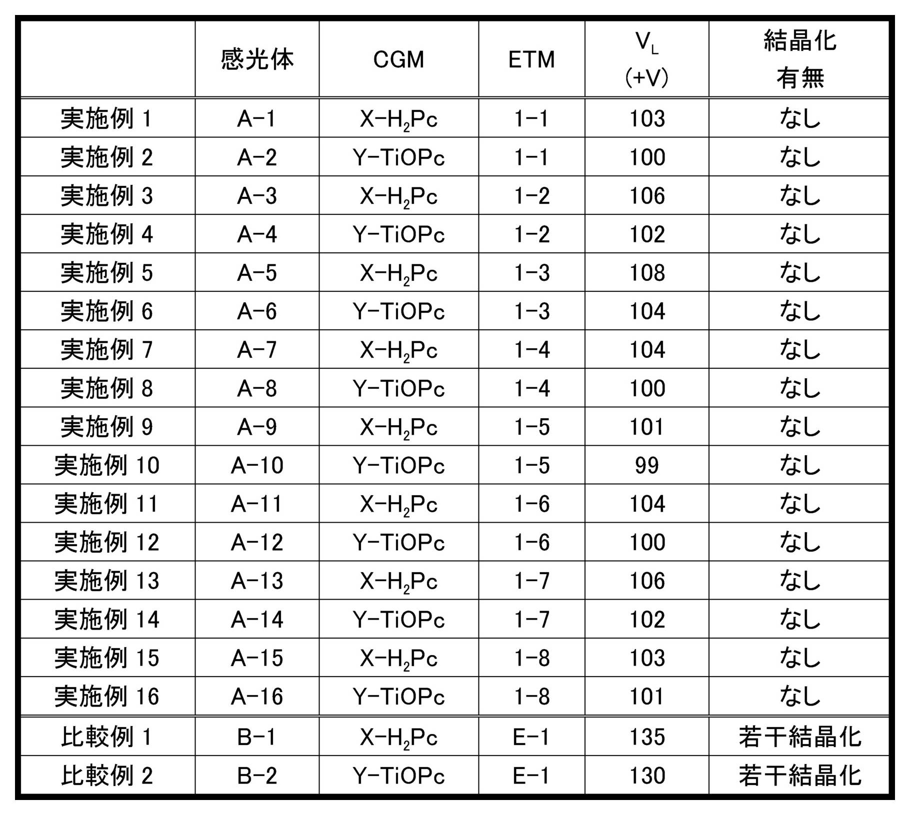
感光体(A-1)~(A-16)は、導電性基体と、単層の感光層とを備えていた。感光層は、電荷発生剤と化合物(1)とを少なくとも含有していた。具体的には、感光層は、一般式(1)に包含される化合物(1-1)~(1-8)の何れかを含有していた。表3から明らかなように、感光体(A-1)~(A-16)の露光後電位は、+108V以下であった。また、感光体(A-1)~(A-16)の感光層は、結晶化した部分が確認されなかった。
一方、感光体(B-1)~(B-2)の感光層は、化合物(1)が含有されていなかった。具体的には、感光体(B-1)~(B-2)の感光層には化合物(E-1)が含有されていたが、化合物(E-1)は一般式(1)に包含される化合物ではなかった。表3から明らかなように、感光体(B-1)~(B-2)での露光後電位は、+130V以上であった。また、感光体(B-1)~(B-2)の感光層は、結晶化した部分が若干確認された。
以上のことから、感光体(A-1)~(A-16)は、感光体(B-1)~(B-2)と比較して、感度特性に優れていた。また、感光体(A-1)~(A-16)は、感光体(B-1)~(B-2)と比較して、感度特性に優れるだけでなく、感光層の結晶化が抑制されていた。
本発明に係る感光体は、画像形成装置に利用することができる。
Claims (9)
- 導電性基体と、単層の感光層とを備え、
前記感光層は、電荷発生剤と、一般式(1)で表される化合物とを少なくとも含有する、電子写真感光体。

前記一般式(1)中のR1、及び前記一般式(Z2)中のR1は、
炭素原子数1以上10以下のアルキル基で置換されてもよい炭素原子数6以上22以下のアリール基、
炭素原子数7以上20以下のアラルキル基、
炭素原子数3以上20以下のシクロアルキル基、
炭素原子数1以上6以下のアルコキシ基、又は
-CO-OR2基で置換されてもよい炭素原子数3以上30以下のアルキル基を表し、R2は、炭素原子数1以上8以下のアルキル基を表す。)
- 前記一般式(1)中のR1、及び前記一般式(Z2)中のR1は、
炭素原子数1以上10以下のアルキル基で置換されてもよい炭素原子数6以上22以下のアリール基、
炭素原子数7以上20以下のアラルキル基、又は
-CO-OR2基で置換されてもよい炭素原子数3以上30以下のアルキル基を表し、R2は、炭素原子数1以上8以下のアルキル基を表す、請求項1に記載の電子写真感光体。 - 前記一般式(1)中のR1、及び前記一般式(Z2)中のR1は、-CO-OR2基で置換されてもよい炭素原子数3以上30以下のアルキル基を表し、R2は、炭素原子数1以上8以下のアルキル基を表す、請求項1に記載の電子写真感光体。
- 前記一般式(1)で表される化合物は、化学式(1-1)、(1-2)、(1-3)、又は(1-4)で表される化合物である、請求項1に記載の電子写真感光体。
- 前記一般式(1)で表される化合物は、化学式(1-5)、(1-6)、(1-7)、又は(1-8)で表される化合物である、請求項1に記載の電子写真感光体。

- 前記一般式(1)で表される化合物は、前記化学式(1-5)で表される化合物である、請求項5に記載の電子写真感光体。
- 前記感光層は、一般式(10)で表される化合物を更に含有する、請求項1に記載の電子写真感光体。
a、b、c、及びdは、各々独立に、0以上5以下の整数を表し、
e、及びfは、各々独立に、0以上4以下の整数を表す。) - 前記一般式(10)で表される化合物は、化学式(10-1)で表される化合物である、請求項7に記載の電子写真感光体。
- 前記感光層は、化学式(20)で表される繰り返し単位を有するポリカーボネート樹脂を更に含有する、請求項1に記載の電子写真感光体。

Priority Applications (2)
| Application Number | Priority Date | Filing Date | Title |
|---|---|---|---|
| CN201980069035.1A CN112930499B (zh) | 2018-10-23 | 2019-08-29 | 电子照相感光体 |
| JP2020552569A JP7078130B2 (ja) | 2018-10-23 | 2019-08-29 | 電子写真感光体 |
Applications Claiming Priority (2)
| Application Number | Priority Date | Filing Date | Title |
|---|---|---|---|
| JP2018-199336 | 2018-10-23 | ||
| JP2018199336 | 2018-10-23 |
Publications (1)
| Publication Number | Publication Date |
|---|---|
| WO2020084900A1 true WO2020084900A1 (ja) | 2020-04-30 |
Family
ID=70331349
Family Applications (1)
| Application Number | Title | Priority Date | Filing Date |
|---|---|---|---|
| PCT/JP2019/033948 Ceased WO2020084900A1 (ja) | 2018-10-23 | 2019-08-29 | 電子写真感光体 |
Country Status (3)
| Country | Link |
|---|---|
| JP (1) | JP7078130B2 (ja) |
| CN (1) | CN112930499B (ja) |
| WO (1) | WO2020084900A1 (ja) |
Citations (4)
| Publication number | Priority date | Publication date | Assignee | Title |
|---|---|---|---|---|
| JPS6073542A (ja) * | 1983-09-29 | 1985-04-25 | Toyo Ink Mfg Co Ltd | 光半導体素子 |
| JPH052277A (ja) * | 1991-06-24 | 1993-01-08 | Nippon Chibagaigii Kk | 電子写真感光体 |
| JP2011059371A (ja) * | 2009-09-10 | 2011-03-24 | Ricoh Co Ltd | 電子写真感光体、電子写真方法、電子写真装置、並びに電子写真装置用プロセスカートリッジ |
| JP2011197139A (ja) * | 2010-03-17 | 2011-10-06 | Ricoh Co Ltd | 電子写真感光体、電子写真方法、電子写真装置、並びに電子写真装置用プロセスカートリッジ |
Family Cites Families (2)
| Publication number | Priority date | Publication date | Assignee | Title |
|---|---|---|---|---|
| JP2012073346A (ja) * | 2010-09-28 | 2012-04-12 | Kyocera Mita Corp | 電子写真感光体 |
| CN106750196B (zh) * | 2017-01-06 | 2019-02-01 | 天津大学 | 基于异靛蓝衍生物的电子传输型聚合物及有机场效应晶体管 |
-
2019
- 2019-08-29 WO PCT/JP2019/033948 patent/WO2020084900A1/ja not_active Ceased
- 2019-08-29 JP JP2020552569A patent/JP7078130B2/ja not_active Expired - Fee Related
- 2019-08-29 CN CN201980069035.1A patent/CN112930499B/zh active Active
Patent Citations (4)
| Publication number | Priority date | Publication date | Assignee | Title |
|---|---|---|---|---|
| JPS6073542A (ja) * | 1983-09-29 | 1985-04-25 | Toyo Ink Mfg Co Ltd | 光半導体素子 |
| JPH052277A (ja) * | 1991-06-24 | 1993-01-08 | Nippon Chibagaigii Kk | 電子写真感光体 |
| JP2011059371A (ja) * | 2009-09-10 | 2011-03-24 | Ricoh Co Ltd | 電子写真感光体、電子写真方法、電子写真装置、並びに電子写真装置用プロセスカートリッジ |
| JP2011197139A (ja) * | 2010-03-17 | 2011-10-06 | Ricoh Co Ltd | 電子写真感光体、電子写真方法、電子写真装置、並びに電子写真装置用プロセスカートリッジ |
Non-Patent Citations (3)
| Title |
|---|
| JIANG ET AL.: "Synthesis and Characterization of Isoindigo [7,6-g] isoindigo-Based Donor-Acceptor Conjugated Polymers", MACROMOLECULES, vol. 49, no. 6, 10 March 2016 (2016-03-10), pages 2135 - 2144, XP055710243 * |
| RANDELL ET AL.: "Bisisoindigo:using a ring-fusion approach to extend the conjugation length of isoindigo", JOURNAL OF MATERIALS CHEMISTRY A, vol. 4, no. 18, 2016, pages 6940 - 6945, XP055710247 * |
| RANDELL ET AL.: "Effect of Acceptor Unit Length and Planarity on the Optoelectronic Properties of Isoindigo-Thiophene Donor-Acceptor Polymers", CHEMISTRY OF MATERIALS, vol. 30, no. 14, 20 June 2018 (2018-06-20), pages 4864 - 4873, XP055710236 * |
Also Published As
| Publication number | Publication date |
|---|---|
| CN112930499A (zh) | 2021-06-08 |
| JP7078130B2 (ja) | 2022-05-31 |
| CN112930499B (zh) | 2023-12-29 |
| JPWO2020084900A1 (ja) | 2021-09-09 |
Similar Documents
| Publication | Publication Date | Title |
|---|---|---|
| JP6358241B2 (ja) | ナフタレンジカルボイミド誘導体及び電子写真感光体 | |
| JP6881335B2 (ja) | キノン誘導体及び電子写真感光体 | |
| JP7078130B2 (ja) | 電子写真感光体 | |
| CN108153120B (zh) | 电子照相感光体 | |
| JP2018013574A (ja) | 電子写真感光体 | |
| JP7135619B2 (ja) | 電子写真感光体 | |
| JP2018013573A (ja) | 電子写真感光体 | |
| JP2019078978A (ja) | 電子写真感光体 | |
| CN108572518B (zh) | 电子照相感光体 | |
| JP2019191414A (ja) | アゾキノン誘導体及び電子写真感光体 | |
| JP6702500B2 (ja) | 電子写真感光体 | |
| JP6885469B2 (ja) | 電子写真感光体 | |
| CN108873628B (zh) | 电子照相感光体 | |
| JP6702444B2 (ja) | 電子写真感光体 | |
| JP2022018812A (ja) | シアノ基含有化合物及び電子写真感光体 | |
| JP6583242B2 (ja) | 電子写真感光体 | |
| JP2021006512A (ja) | シアノ基含有化合物及び電子写真感光体 | |
| JP6617690B2 (ja) | 電子写真感光体 | |
| JP2017198833A (ja) | キノン誘導体及び電子写真感光体 | |
| JP2021056348A (ja) | 電子写真感光体 | |
| JP2021008440A (ja) | 環状ジエステル化合物及び電子写真感光体 | |
| JP2022018811A (ja) | シアノ基含有化合物及び電子写真感光体 | |
| JP2022018813A (ja) | シアノ基含有化合物及び電子写真感光体 | |
| JP2019189555A (ja) | キノン誘導体及び電子写真感光体 | |
| JP2018091988A (ja) | 電子写真感光体 |
Legal Events
| Date | Code | Title | Description |
|---|---|---|---|
| 121 | Ep: the epo has been informed by wipo that ep was designated in this application |
Ref document number: 19875807 Country of ref document: EP Kind code of ref document: A1 |
|
| ENP | Entry into the national phase |
Ref document number: 2020552569 Country of ref document: JP Kind code of ref document: A |
|
| NENP | Non-entry into the national phase |
Ref country code: DE |
|
| 122 | Ep: pct application non-entry in european phase |
Ref document number: 19875807 Country of ref document: EP Kind code of ref document: A1 |