WO2020084877A1 - 吸着機構、切断装置および切断品の製造方法 - Google Patents
吸着機構、切断装置および切断品の製造方法 Download PDFInfo
- Publication number
- WO2020084877A1 WO2020084877A1 PCT/JP2019/032391 JP2019032391W WO2020084877A1 WO 2020084877 A1 WO2020084877 A1 WO 2020084877A1 JP 2019032391 W JP2019032391 W JP 2019032391W WO 2020084877 A1 WO2020084877 A1 WO 2020084877A1
- Authority
- WO
- WIPO (PCT)
- Prior art keywords
- metal foam
- suction
- suction mechanism
- jig
- cut
- Prior art date
- Legal status (The legal status is an assumption and is not a legal conclusion. Google has not performed a legal analysis and makes no representation as to the accuracy of the status listed.)
- Ceased
Links
Images







Classifications
-
- B—PERFORMING OPERATIONS; TRANSPORTING
- B23—MACHINE TOOLS; METAL-WORKING NOT OTHERWISE PROVIDED FOR
- B23Q—DETAILS, COMPONENTS, OR ACCESSORIES FOR MACHINE TOOLS, e.g. ARRANGEMENTS FOR COPYING OR CONTROLLING; MACHINE TOOLS IN GENERAL CHARACTERISED BY THE CONSTRUCTION OF PARTICULAR DETAILS OR COMPONENTS; COMBINATIONS OR ASSOCIATIONS OF METAL-WORKING MACHINES, NOT DIRECTED TO A PARTICULAR RESULT
- B23Q3/00—Devices holding, supporting, or positioning work or tools, of a kind normally removable from the machine
- B23Q3/02—Devices holding, supporting, or positioning work or tools, of a kind normally removable from the machine for mounting on a work-table, tool-slide, or analogous part
- B23Q3/06—Work-clamping means
- B23Q3/08—Work-clamping means other than mechanically-actuated
-
- B—PERFORMING OPERATIONS; TRANSPORTING
- B26—HAND CUTTING TOOLS; CUTTING; SEVERING
- B26D—CUTTING; DETAILS COMMON TO MACHINES FOR PERFORATING, PUNCHING, CUTTING-OUT, STAMPING-OUT OR SEVERING
- B26D7/00—Details of apparatus for cutting, cutting-out, stamping-out, punching, perforating, or severing by means other than cutting
- B26D7/20—Cutting beds
-
- B—PERFORMING OPERATIONS; TRANSPORTING
- B28—WORKING CEMENT, CLAY, OR STONE
- B28D—WORKING STONE OR STONE-LIKE MATERIALS
- B28D5/00—Fine working of gems, jewels, crystals, e.g. of semiconductor material; apparatus or devices therefor
- B28D5/02—Fine working of gems, jewels, crystals, e.g. of semiconductor material; apparatus or devices therefor by rotary tools, e.g. drills
-
- B—PERFORMING OPERATIONS; TRANSPORTING
- B28—WORKING CEMENT, CLAY, OR STONE
- B28D—WORKING STONE OR STONE-LIKE MATERIALS
- B28D7/00—Accessories specially adapted for use with machines or devices of the preceding groups
- B28D7/04—Accessories specially adapted for use with machines or devices of the preceding groups for supporting or holding work or conveying or discharging work
Definitions
- the present disclosure relates to an adsorption mechanism, a cutting device, and a method for manufacturing a cut product.
- Patent Document 1 describes a cutting chuck for use with a cutting blade and for holding a semiconductor wafer.
- the cutting chuck described in Patent Document 1 includes a porous layer formed of a ceramic such as alumina and a surface layer on the porous layer, and a semiconductor wafer is adsorbed on the surface layer (see FIG. 5 etc.).
- a pump arranged below the porous layer sucks a semiconductor wafer on the surface layer by sucking through a vacuum passage provided inside the surface layer and the pores of the porous layer. Adsorb.
- the cutting chuck described in Patent Document 1 divides a semiconductor wafer by dicing and divides the semiconductor wafer, and holds suction until the divided semiconductor wafer is picked up.
- the porous layer formed of ceramic does not have a high porosity, and the adsorption force locally decreases, resulting in adsorption.
- the unevenness may occur.
- suction unevenness occurs on the cutting chuck, the semiconductor package after cutting the semiconductor package substrate may be scattered from the cutting chuck.
- a suction mechanism that includes a chamber, a jig inside the chamber, and a suction portion on the jig, and the jig includes a metal foam.
- a step of cutting the cutting object by the cutting device and a step of adsorbing and conveying the cutting object cut in the cutting step by the suction mechanism
- a method for manufacturing a cut product can be provided.
- FIG. 6 is a schematic plan view illustrating a region of a metal foam used for measuring surface flatness after long-term use as a jig of an adsorption mechanism. It is the result of measuring the flatness of the surface of the metal foam after long-term use as a jig for an adsorption mechanism.
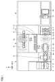
- FIG. 1 shows a schematic plan view of the electronic component manufacturing apparatus of the embodiment.
- the electronic component manufacturing apparatus of the embodiment shown in FIG. 1 includes a substrate supply device A, a cutting device B, a cleaning device C, and a transfer device D.
- the substrate supply device A mounts an in-magazine 1 for loading a semiconductor package substrate 5 which is an example of an object to be cut according to the embodiment, and a semiconductor package substrate 5 taken out from the in-magazine 1.
- the board supply device A operates as follows, for example. First, the semiconductor package substrate 5 loaded in the in-magazine 1 is placed on the substrate supply table 7. Next, the strip rail loader 6 located above the semiconductor package substrate 5 in the Z-axis direction holds the semiconductor package substrate 5 on the supply table 7. Next, the strip rail loader 6 moves to the cutting device B along the strip rail 6a in the X-axis direction while holding the semiconductor package substrate 5. After that, the strip rail loader 6 places the semiconductor package substrate 5 on the cut table 8 of the cutting device B below in the Z-axis direction. This completes the operation of the substrate supply apparatus A.
- FIG. 2 shows a schematic cross-sectional view of an example of the semiconductor package substrate 5 used as a cutting target of the electronic component manufacturing apparatus of the embodiment.
- the semiconductor package substrate 5 includes, for example, the support member 3 and the sealing resin 4 on at least a part of the support member 3.
- the support member 3 is a member that supports, for example, a semiconductor chip or a thin film, and is a lead frame, a substrate, an interposer, a semiconductor substrate (Si wafer or the like), a metal substrate, a glass substrate, a ceramic substrate, a resin substrate, or wiring.
- the substrate may be included and may or may not be wired.
- the sealing resin 4 is a resin that seals at least one surface of the semiconductor chip or the thin film supported by the support member 3.
- the cutting target object is not limited to the semiconductor package substrate 5.
- the cutting device B includes a cut table 8 for mounting the semiconductor package substrate 5 before cutting or the semiconductor package 5a after cutting, and a rotating mechanism 8a for rotating the cut table 8.
- a moving mechanism (not shown) for moving the cut table 8 and the rotating mechanism 8a, a spindle 9 having a blade (not shown) for cutting the semiconductor package substrate 5, and the base 3 side of the semiconductor package 5a.
- a cleaning water spraying member 11 for spraying the cleaning water and an air spraying member 12 for drying the cleaning water sprayed on the base material 3 side of the semiconductor package 5a are provided.
- FIG. 3 shows a schematic cross-sectional view of an example of a suction mechanism used in the cut table 8 of the electronic component manufacturing apparatus of the embodiment.
- the suction mechanism 100 includes a chamber 34, a jig 33 in the chamber 34, a suction portion 31 on the jig 33, a flow path 35 below the jig 33, and a suction force of the suction portion 31.
- a suction mechanism 36 such as a vacuum pump for sucking gas such as vacuuming through the flow path 35 to exert the effect.
- the chamber 34 has an outer wall 34a and a bottom surface 34b.
- the outer wall 34a is located so as to surround the side of the internal space in which the jig 33 is placed.
- the bottom surface 34b is located so as to face the suction portion 31 via the jig 33, and the outer edge of the bottom surface 34b is connected to the outer wall 34a.
- the configuration of the chamber 34 is not particularly limited as long as the jig 33 can be supported and the suction force can be generated by the suction mechanism 36 via the jig 33. .
- the suction part 31 includes a base material part 31a such as a metal plate and a suction pad part 31b such as rubber on the base material part 31a.
- the base material portion 31a and the suction pad portion 31b may be joined by being integrated, for example.
- the suction portion 31 is provided with a suction hole 38 that vertically penetrates a part of each of the base material portion 31a and the suction pad portion 31b, and the suction pad portion 31b corresponds to a cut portion of the semiconductor package substrate 5.
- the groove portion 39 is provided at the position to be filled.
- the configuration of the suction unit 31 is not particularly limited as long as it can be supported by the jig 33 and a suction force can be generated through the jig 33 by suction of the suction mechanism 36.
- the jig 33 has a metal foam.
- the jig 33 is located in the inner space of the chamber 34 surrounded by the outer wall 34a and the bottom surface 34b on the opposite side of the suction pad 31b of the suction portion 31.
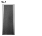
- FIG. 4 shows a photograph of an example of metal foam used for the jig 33 of the suction mechanism of the embodiment.
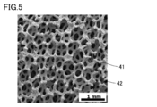
- FIG. 5 shows an enlarged photograph of the metal foam shown in FIG.
- the metal foam includes a skeleton having a three-dimensional mesh structure, and the skeleton includes a plurality of struts 41. Pores 42 are located between the struts 41.
- Each of the plurality of struts 41 may be made of a metal-containing material.
- FIGS. 6 and 7 show enlarged photographs of another example of the metal foam.
- at least one of the metal foam struts 41 includes a hollow structure 43.
- the coating layer 44 is located on the outer surface of the strut 41.
- the coating layer 44 may contain a fluorine-based resin such as polytetrafluoroethylene (PTFE) in order to provide the metal foam with rust resistance.
- PTFE polytetrafluoroethylene
- the fluorine-based resin is not limited to PTFE, and a resin containing fluorine that imparts rust resistance to metal foam can be used.
- the “rust resistance performance” means performance capable of suppressing corrosion of the outer surface of the strut 41.
- the metal foam may contain nickel as a main component, for example.
- nickel as a main component means that the metal atom constituting 50 atom% or more of the metal foam is nickel. It can be confirmed, for example, by secondary ion mass spectrometry (SIMS) that nickel is a metal atom that constitutes 50 atomic% or more of the metal foam.
- SIMS secondary ion mass spectrometry
- the metal foam may contain, for example, chromium, aluminum, or both chromium and aluminum. Further, the metal foam may contain an alloy of nickel, chromium and aluminum. Further, the metal foam may contain a non-ferrous metal or may contain iron. The presence of metal atoms such as chromium, aluminum or iron in the metal foam can also be confirmed by SIMS, for example.
- the porosity of the metal foam may be 90% or more.
- the porosity of the metal foam is 90% or more, the gas sucked by the suction mechanism 36 easily passes through the jig 33, and the suction force of the suction portion 31 tends to be improved.
- the porosity of the metal foam may be 98% or less.
- the porosity of the metal foam is 98% or less, the jig 33 that supports the adsorption portion 31 has higher strength, and the jig 33 tends to be usable for a longer period of time.
- the porosity of the metal foam can be determined as follows. First, the weight and volume of the metal foam are measured. Next, from the measured weight value (weight measurement value [g]) and volume measurement value (volume measurement value [cm 3 ]) of the metal foam, the measured density [g / cm 3 ] of the metal foam is calculated as follows. It is calculated by the equation (I).
- Measurement density [g / cm 3 ] (weight measurement value [g]) / (volume measurement value [cm 3 ]) (I)
- the theoretical density of the metal forming the metal foam (the density assuming that the metal foam has no pores 42) [g / cm 3 ] is determined.
- the porosity [%] of the metal foam is calculated by the following formula (II) using the measured density [g / cm 3 ] and the theoretical density [g / cm 3 ] obtained by the above formula (I). .
- Porosity [%] of metal foam 100 ⁇ [1- ⁇ (measured density [g / cm 3 ]) / (theoretical density [g / cm 3 ]) ⁇ ] (II)
- the porosity [%] of the metal foam is From the formula (II), 100 ⁇ ⁇ 1 ⁇ (0.33 / 8.4) ⁇ ⁇ 96 [%].
- the porosity of the metal foam obtained above can also be applied to the porosity of the metal foam when at least a part of the plurality of struts 41 has a hollow structure. Further, the porosity of the metal foam obtained above does not take into consideration the existence of the coating layer 44 on the outer surface of the strut 41, but the porosity of the metal foam when the coating layer 44 exists on the outer surface of the strut 41. The porosity of the foam is considered to be almost the same as the porosity of the metal foam calculated above.
- the cell size of the metal foam may be 1000 ⁇ m or more, or 3000 ⁇ m or more.
- the jig 33 supporting the suction part 31 has higher strength, and the jig 33 tends to be usable for a longer period of time.
- the cell size of the metal foam may be 6000 ⁇ m or less.
- the gas sucked by the suction mechanism 36 easily passes through the jig 33, the suction force of the suction portion 31 is improved, and the jig for supporting the suction portion 31 is improved.
- 33 has higher strength, and the jig 33 tends to be usable for a longer period of time.
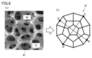
- the cell size of metal foam can be calculated as follows. First, an enlarged photograph of a metal foam as shown in FIG. 8A is obtained. Next, as shown in FIG. 8B, a model in which the metal foam cell 51 is planarized is produced from the enlarged photograph of FIG. 8A.
- the outer edge of the cell 51 of the flattened model constitutes a decagon, and a line segment connecting any two points on the decagon of the outer edge of the cell 51.
- the length a of the longest line segment AA ′ and the length b of the line segment BB ′ orthogonal to the line segment AA ′ are measured.
- the square root of the product of the length a [ ⁇ m] of the line segment AA ′ and the length b [ ⁇ m] of the line segment BB ′ measured as described above is expressed by the following formula (III).
- the skeleton of the metal foam three-dimensional mesh structure has the dodecahedron cells 51 as one constituent unit.
- One cell 51 is composed of 30 struts 41. Of these struts 41, five struts 41 form a pentagon to form one pore 42, and one cell 51 has 12 pores 42.
- Figure 9 shows a photograph of an example of metal foam with a cell size of approximately 3000 ⁇ m.
- FIG. 10 shows a photograph of an example of metal foam having a cell size of about 6000 ⁇ m.
- the metal foam can be produced, for example, by the method described in Patent Document 2 (Japanese Patent Publication No. 2006-522215) or Patent Document 3 (Japanese Patent Publication 2007-502368).
- Patent Document 2 Japanese Patent Publication No. 2006-522215
- Patent Document 3 Japanese Patent Publication 2007-502368
- the metal foam for example, a metal foam manufactured by AL Antum can be used.
- the alloy of nickel, chrome, and aluminum having a square surface of 50 mm in length and 50 mm in width produced by changing the parameters of the cell size [ ⁇ m], the thickness [mm], and the presence or absence of the coating layer of the metal foam described above.
- Sample No. of metal foam 1 to No. The compressive strength [MPa] was measured for each of the six. The results are shown in Table 1 below.
- a universal material testing machine (UTM: Universal Testing Machine) manufactured by Daekyung Tech of South Korea was used to measure the compressive strength.
- the metal foam of No. 6 had a high compressive strength within the range of 0.24 to 1.05 MPa. It is considered that not only the metal foam having a cell size of 1000 ⁇ m but also the metal foam having a good gas permeability of 6000 ⁇ m, which has a cell size of 6000 ⁇ m, has higher compressive strength than a ceramic having a similar gas permeability. Therefore, it is considered that the suction mechanism 100 of the embodiment in which the metal foam is used for the jig 33 can be used for a long time as compared with the case where the jig 33 is made of ceramic.
- the metal foam is divided into 12 areas in the vertical direction and 6 areas in the horizontal direction, and the suction mechanism 100 using the metal foam as the jig 33 is used for a long time. After that, the flatness of each area of the surface of the metal foam was measured.
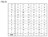
- FIGS. 12 and 13 It should be noted that the numerical values 1 to 12 existing in the upper direction of the "region" column in FIG. 12 mean 12 regions in the vertical direction of the metal foam shown in FIG. Further, the numerical values 1 to 6 existing to the right of the "region” column in FIG. 12 mean the six regions in the lateral direction of the metal foam shown in FIG. Numerical values other than the upward direction and the rightward direction in the “region” column of FIG.
- FIG. 12 shows the numerical values of the height difference in FIG.
- the height of the surface of the region where the vertical region 10 and the horizontal region 4 intersect is the highest (+12 ⁇ m)
- the height of the surface of the region where the vertical region 8 and the horizontal region 2 intersect is the lowest (-27 ⁇ m)
- the maximum height difference is 39 ⁇ m. It is considered that the value of this height difference can be significantly reduced as compared with the case where ceramic having the same gas permeability is used instead of metal foam for the same period.
- the flatness of the surface of metal foam is considered as follows. Since the metal foam has a skeleton having a three-dimensional mesh structure made of metal, it has excellent strength almost evenly against a load from any direction. Therefore, it is considered that the use of metal foam can maintain good flatness for normal use. Further, if it is made of brittle ceramic, it is easily broken when a load is applied and its flatness is lowered, but since the metal foam is made of metal, such flatness does not easily occur.
- the cutting device B having the cutting table 8 including the suction mechanism 100 of the embodiment using the above-mentioned metal foam as the jig 33 shown in FIG. 3 operates as follows, for example. First, as shown in FIG. 1, the cut table 8 on which the semiconductor package substrate 5 before cutting is placed is moved in the Y-axis direction by a moving mechanism (not shown).
- the cut table 8 on which the semiconductor package substrate 5 is placed is moved to the spindle 9 in the X-axis direction.
- the cut table 8 is rotated by the rotation mechanism 8a so as to match the cutting direction of the semiconductor package substrate 5.
- the blade 30 attached to the spindle 9 is positioned above the semiconductor package substrate 5.
- the suction mechanism 36 sucks the semiconductor package substrate 5 on the suction pad portion 31b through the flow path 35, the jig 33, and the suction hole 38 to suck the semiconductor package substrate 5 on the suction pad portion 31b.
- the blade 30 is rotated by the spindle 9, the blade 30 is brought into contact with the semiconductor package substrate 5 on the cut table 8 and cut.
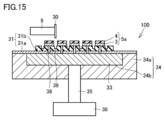
- a plurality of semiconductor packages 5a obtained by cutting the semiconductor package substrate 5 into individual pieces as shown in the schematic sectional view of FIG. 15 are obtained.
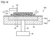
- the cutting position of the semiconductor package substrate 5 by the blade 30 corresponds to a position above the groove portion 39 of the suction pad portion 31b.
- cleaning water is sprayed by the cleaning water spraying member 11 onto the supporting member 3 side of the semiconductor packages 5a which are diced on the cut table 8.
- the cleaning water sprayed on the support member 3 side of the semiconductor package 5a is blown off by injecting air from the air injection member 12 to dry the semiconductor package 5a.
- the semiconductor package 5a on the cut table 8 is moved to the cleaning device C. This completes the operation of the cutting device B.
- the cleaning device C includes a package unloader 13 for holding the semiconductor package 5a, a mold cleaner 16 for cleaning the sealing resin 4 side of the semiconductor package 5a, and a sealing resin 4 side of the semiconductor package 5a for drying.
- the cleaning device C operates as follows, for example. First, the package unloader 13 holds the semiconductor package 5a and pulls it up from the cut table 8 in the Z-axis direction. Next, the package unloader 13 moves the semiconductor package 5a in the X-axis direction to move the mold cleaner 16 and the air injection member 17 to a position above the Z-axis direction. Then, the mold cleaner 16 cleans the sealing resin 4 side of the semiconductor package 5a, and the air spraying member 17 sprays air to dry the sealing resin 4 side of the semiconductor package 5a. This completes the operation of the cleaning device C.
- the carrier device D includes a flipper 14 for holding and reversing the semiconductor package 5a, an index table 15 for mounting the semiconductor package 5a reversed by the flipper 14, and a moving mechanism for moving the index table 15. (Not shown).
- the index table 15 can be accommodated in a main member such as a tray using a moving mechanism, and at this time, good products and defective products can be distinguished and accommodated in different accommodation members.
- the cutting device B of the electronic component manufacturing apparatus uses the cut table 8 including the suction mechanism 100 according to the embodiment using a metal foam for the jig 33 as shown in FIG. 3, for example. Therefore, in the electronic component manufacturing apparatus of the embodiment, as compared with the case where the cutting chuck described in Patent Document 1 using the conventional porous layer formed of ceramic is used as the cutting table 8, the suction of the cutting table 8 is increased. The unevenness can be reduced, and the suction mechanism 100 can be used for a long time. Further, by reducing the suction unevenness of the cut table 8, it is possible to suppress the scattering of the semiconductor package 5a from the cut table 8. Further, even when the suction mechanism 100 is used for a long period of time, it is possible to maintain the flatness of the surface of the jig 33 at a high level.
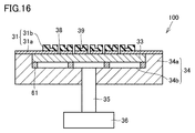
- FIG. 16 shows a schematic cross-sectional view of a modified example of the suction mechanism 100 of the embodiment.
- a modification of the suction mechanism 100 of the embodiment shown in FIG. 16 is characterized in that a support portion 61 is provided between the jig 33 and the bottom surface 34b of the chamber 34. Also in this case, it is possible to reduce the suction unevenness of the cut table 8 as compared with the case where the cutting chuck described in Patent Document 1 using a porous layer formed of a conventional ceramic is used for the cut table 8.
- the suction mechanism 100 can be used for a long time. Further, by reducing the suction unevenness of the cut table 8, it is possible to suppress the scattering of the semiconductor package 5a from the cut table 8. Further, even when the suction mechanism 100 is used for a long period of time, it is possible to maintain the flatness of the surface of the jig 33 at a high level.
- the suction mechanism 100 of the embodiment in which the metal foam is used for the jig 33 is used for the cut table 8 of the cutting device B is explained.
- the suction mechanism 100 of the embodiment is not limited to the cut table 8.
- adsorption unevenness can be suppressed and long-term use is possible, as compared with the case where the cutting chuck described in Patent Document 1 using a porous layer formed of a conventional ceramic is used. Become.
Landscapes
- Engineering & Computer Science (AREA)
- Mechanical Engineering (AREA)
- Life Sciences & Earth Sciences (AREA)
- Forests & Forestry (AREA)
- Container, Conveyance, Adherence, Positioning, Of Wafer (AREA)
- Processing Of Stones Or Stones Resemblance Materials (AREA)
- Dicing (AREA)
- Jigs For Machine Tools (AREA)
- Details Of Cutting Devices (AREA)
Abstract
吸着機構(100)は、チャンバ(34)と、チャンバ(34)内のジグ(33)と、ジグ(33)上の吸着部(31)とを備えている。ジグ(33)はメタルフォームを備える。切断装置(B)は、吸着機構(100)を備える。切断品の製造方法は、切断装置(B)により切断対象物(5)を切断する工程と、切断する工程において切断された切断対象物(5)を吸着機構(100)により吸着して搬送する工程とを備える。
Description
本開示は、吸着機構、切断装置および切断品の製造方法に関する。
たとえば特許文献1には、切断ブレードとともに用いるための、および半導体ウエハを保持するための切断チャックが記載されている。特許文献1に記載の切断チャックは、アルミナ等のセラミックから形成された多孔質層と、多孔質層上の表面層とを備えており、表面層において半導体ウエハを吸着する(特許文献1の図5等)。
特許文献1に記載の切断チャックは、多孔質層の下方に配置されたポンプが、表面層の内部に設けられた真空通路および多孔質層の多孔を通して吸引することによって表面層上の半導体ウエハを吸着する。特許文献1に記載の切断チャックは、半導体ウエハをダイシングして分割し、分割後の半導体ウエハがピックアップされるまで吸着を保持する。
しかしながら、特許文献1に記載の切断チャックを半導体パッケージの吸着に用いた場合には、セラミックから形成された多孔質層が高い気孔率を有さず、吸着力が局所的に低下して、吸着ムラが生じることがあった。切断チャックに吸着ムラが生じた場合には、半導体パッケージ基板の切断後の半導体パッケージが切断チャックから飛散することがあった。
その一方で、特許文献1に記載の切断チャックの多孔質層に高い気孔率を有するセラミックを用いた場合には、多孔質層が脆くなって所定の強度を確保することができず、長期間使用できないことがあった。
ここで開示された実施形態によれば、チャンバと、チャンバ内のジグと、ジグ上の吸着部とを備え、ジグはメタルフォーム(Metal Foam)を備える吸着機構を提供することができる。
ここで開示された実施形態によれば、上記の吸着機構を備える切断装置を提供することができる。
ここで開示された実施形態によれば、上記の切断装置により切断対象物を切断する工程と、切断する工程において切断された切断対象物を上記の吸着機構により吸着して搬送する工程とを備える切断品の製造方法を提供することができる。
ここで開示された実施形態によれば、吸着ムラを低減することが可能であり、長期間使用することが可能な吸着機構、切断装置および切断品の製造方法を提供することができる。
以下、実施形態について説明する。なお、実施形態の説明に用いられる図面において、同一の参照符号は、同一部分または相当部分を表わすものとする。
図1に、実施形態の電子部品製造装置の模式的な平面図を示す。図1に示す実施形態の電子部品製造装置は、基板供給装置Aと、切断装置Bと、洗浄装置Cと、搬送装置Dとを備えている。
図1に示すように、基板供給装置Aは、実施形態の切断対象物の一例である半導体パッケージ基板5を装填するためのインマガジン1と、インマガジン1から取り出された半導体パッケージ基板5を載置するための基板供給テーブル7と、半導体パッケージ基板5を保持して切断装置Bに供給するためのストリップレールローダ6と、ストリップレールローダ6が切断装置Bまで移動するためのストリップレール6aと、を備えている。
基板供給装置Aは、たとえば以下のように動作する。まず、インマガジン1に装填されている半導体パッケージ基板5を基板供給テーブル7上に載置する。次に、半導体パッケージ基板5のZ軸方向上方に位置するストリップレールローダ6が供給テーブル7上の半導体パッケージ基板5を保持する。次に、ストリップレールローダ6は半導体パッケージ基板5を保持した状態でX軸方向にストリップレール6aに沿って切断装置Bまで移動する。その後、ストリップレールローダ6は、Z軸方向下方の切断装置Bのカットテーブル8上に半導体パッケージ基板5を載置する。これにより、基板供給装置Aの動作が完了する。
図2に、実施形態の電子部品製造装置の切断対象物として用いられる半導体パッケージ基板5の一例の模式的な断面図を示す。図2に示すように、半導体パッケージ基板5は、たとえば、支持部材3と、支持部材3の少なくとも一部上の封止樹脂4と、を備える。支持部材3は、たとえば、半導体チップまたは薄膜などを支持する部材であって、リードフレーム、サブストレート、インターポーザ、半導体基板(Siウェハ等)、金属基板、ガラス基板、セラミック基板、樹脂基板、または配線基板を含み、配線が施されていてもよく、配線が施されていなくてもよい。封止樹脂4は、支持部材3に支持された半導体チップまたは薄膜などの少なくとも一面を封止する樹脂である。なお、本実施形態においては切断対象物として半導体パッケージ基板5を用いる場合について説明するが、切断対象物は半導体パッケージ基板5に限定されない。
図1に示すように、切断装置Bは、切断前の半導体パッケージ基板5または切断後の半導体パッケージ5aを載置するためのカットテーブル8と、カットテーブル8を回転させるための回転機構8aと、カットテーブル8および回転機構8aを移動させるための移動機構(図示せず)と、半導体パッケージ基板5を切断するためのブレード(図示せず)を有するスピンドル9と、半導体パッケージ5aの基材3側に洗浄水を噴霧するための洗浄水噴霧部材11と、半導体パッケージ5aの基材3側に噴霧された洗浄水を乾燥するためのエア噴射部材12とを備えている。
図3に、実施形態の電子部品製造装置のカットテーブル8に用いられる吸着機構の一例の模式的な断面図を示す。図3に示すように、吸着機構100は、チャンバ34と、チャンバ34内のジグ33と、ジグ33上の吸着部31と、ジグ33の下方の流路35と、吸着部31の吸着力を発揮させるために流路35を通して真空引き等のガスの吸引をするための真空ポンプ等の吸引機構36と、を備えている。
本実施形態において、チャンバ34は、外壁34aと、底面34bとを備えている。外壁34aは、ジグ33が載置される内部空間の側方を取り囲むように位置している。底面34bは、ジグ33を介して吸着部31と向かい合うように位置しており、底面34bの外縁は外壁34aと連結している。なお、チャンバ34の構成は、ジグ33を支持することが可能であり、吸引機構36の吸引によりジグ33を介して吸着部31に吸着力を生じさせることが可能な構成であれば特に限定されない。
本実施形態において、吸着部31は、メタルプレート等の基材部31aと、基材部31a上のラバー等の吸着パッド部31bとを備えている。基材部31aと吸着パッド部31bとは、たとえば一体化されること等により結合されていてもよい。吸着部31には、基材部31aおよび吸着パッド部31bのそれぞれの一部を鉛直方向に貫通する吸着孔38が設けられており、吸着パッド部31bには半導体パッケージ基板5の切断箇所に対応する位置に溝部39が設けられている。なお、吸着部31の構成も、ジグ33により支持されることが可能であり、吸引機構36の吸引によりジグ33を介して吸着力を生じることが可能な構成であれば特に限定されない。
本実施形態において、ジグ33は、メタルフォームを備えている。ジグ33は、外壁34aおよび底面34bで取り囲まれたチャンバ34の内部空間で吸着部31の吸着パッド部31bとは反対側に位置している。
図4に、実施形態の吸着機構のジグ33に用いられるメタルフォームの一例の写真を示す。図5に、図4に示されるメタルフォームの拡大写真を示す。図5に例示されるようにメタルフォームは、三次元網目構造の骨格を備え、骨格は複数のストラット41を備えている。複数のストラット41の間には気孔42が位置している。複数のストラット41のそれぞれは、金属を含有する材料から構成され得る。
図6および図7に、メタルフォームの他の一例の拡大写真を示す。図6および図7に例示されるように、メタルフォームの複数のストラット41の少なくとも1つは中空構造43を備えている。また、図6および図7に示される例においては、ストラット41の外表面上にはコーティング層44が位置している。コーティング層44は、メタルフォームに耐サビ性能を備えさせるために、たとえばポリテトラフルオロエチレン(PTFE)等のフッ素系樹脂を含有していてもよい。ここで、フッ素系樹脂としては、PTFEに限定されず、メタルフォームに耐サビ性能を与えるフッ素を含む樹脂を用いることができる。なお、「耐サビ性能」とは、ストラット41の外表面の腐食を抑制可能な性能を意味する。
メタルフォームは、たとえばニッケルを主成分として含有していてもよい。なお、「ニッケルを主成分として含有する」とは、メタルフォームの50原子%以上を構成する金属原子がニッケルであることを意味する。ニッケルがメタルフォームの50原子%以上を構成する金属原子であることは、たとえば二次イオン質量分析法(SIMS)によって確認することができる。
メタルフォームは、たとえば、クロム、アルミニウム、またはクロムとアルミニウムとの両方を含有していてもよい。また、メタルフォームは、ニッケルと、クロムと、アルミニウムとの合金を含有していてもよい。また、メタルフォームは、非鉄金属を含有していてもよく、鉄を含有していてもよい。なお、メタルフォーム中のクロム、アルミニウムまたは鉄等の金属原子の存在も、たとえばSIMSによって確認することができる。
メタルフォームの気孔率は、90%以上であってもよい。メタルフォームの気孔率が90%以上である場合には、吸引機構36によって吸引されるガスがジグ33を透過しやすくなって、吸着部31の吸着力が向上する傾向にある。
メタルフォームの気孔率は、98%以下であってもよい。メタルフォームの気孔率が98%以下である場合には、吸着部31を支持するジグ33がより高強度となり、ジグ33をより長期間使用することが可能となる傾向にある。
メタルフォームの気孔率は、以下のようにして求めることができる。まず、メタルフォームの重量および体積をそれぞれ測定する。次に、測定されたメタルフォームの重量の測定値(重量測定値[g])および体積の測定値(体積測定値[cm3])から、メタルフォームの測定密度[g/cm3]を以下の式(I)により求める。
測定密度[g/cm3]=(重量測定値[g])/(体積測定値[cm3]) …(I)
次に、メタルフォームを構成する金属の理論密度(メタルフォームが気孔42を全く有しないと仮定したときの密度)[g/cm3]を求める。
次に、メタルフォームを構成する金属の理論密度(メタルフォームが気孔42を全く有しないと仮定したときの密度)[g/cm3]を求める。
最後に、上記の式(I)で求めた測定密度[g/cm3]と理論密度[g/cm3]とを用いて以下の式(II)によりメタルフォームの気孔率[%]を求める。
メタルフォームの気孔率[%]=100×[1-{(測定密度[g/cm3])/(理論密度[g/cm3])}] …(II)
たとえば、メタルフォームの上記の測定密度が0.33[g/cm3]であり、理論密度が8.4[g/cm3]である場合のメタルフォームの気孔率[%]は、上記の式(II)により、100×{1-(0.33/8.4)}≒96[%]となる。
たとえば、メタルフォームの上記の測定密度が0.33[g/cm3]であり、理論密度が8.4[g/cm3]である場合のメタルフォームの気孔率[%]は、上記の式(II)により、100×{1-(0.33/8.4)}≒96[%]となる。
上記で求められるメタルフォームの気孔率は、複数のストラット41の少なくとも一部が中空構造を有している場合のメタルフォームの気孔率にも適用することができる。また、上記で求められるメタルフォームの気孔率は、ストラット41の外表面上のコーティング層44の存在を考慮していないが、ストラット41の外表面上にコーティング層44が存在している場合のメタルフォームの気孔率も上記で求められるメタルフォームの気孔率とほとんど差がないと考えられる。
メタルフォームのセルサイズは、1000μm以上であってもよく、3000μm以上であってもよい。メタルフォームのセルサイズが1000μm以上または3000μm以上である場合には、吸着部31を支持するジグ33がより高強度となり、ジグ33をより長期間使用することが可能となる傾向にある。
メタルフォームのセルサイズは、6000μm以下であってもよい。メタルフォームのセルサイズが6000μm以下である場合には、吸引機構36によって吸引されるガスがジグ33を透過しやすくなって、吸着部31の吸着力が向上するとともに、吸着部31を支持するジグ33がより高強度となり、ジグ33をより長期間使用することが可能となる傾向にある。
メタルフォームのセルサイズは、以下のようにして求めることができる。まず、図8(a)に示されるようなメタルフォームの拡大写真を取得する。次に、図8(b)に示すように、図8(a)の拡大写真からメタルフォームのセル51を平面化したモデルを作製する。
次に、図8(b)に示されるように、平面化されたモデルのセル51の外縁は10角形を構成しており、セル51の外縁の10角形上の任意の2点を結ぶ線分のうち最も長い線分AA’の長さaと、線分AA’に直交する線分BB’の長さbとを測定する。
最後に、以下の式(III)のように、上記のようにして測定された線分AA’の長さa[μm]と線分BB’の長さb[μm]との積の平方根を求めることによって、メタルフォームのセルサイズ[μm]を求めることができる。
メタルフォームのセルサイズ[μm]=(a×b)1/2 …(III)
なお、メタルフォームの三次元網目構造の骨格は、12面体のセル51を1つの構成単位としている。1つのセル51は30本のストラット41によって構成されている。これらのストラット41のうち5本のストラット41が5角形を形成することによって1つの気孔42が形成され、1つのセル51に12個の気孔42が存在する。
なお、メタルフォームの三次元網目構造の骨格は、12面体のセル51を1つの構成単位としている。1つのセル51は30本のストラット41によって構成されている。これらのストラット41のうち5本のストラット41が5角形を形成することによって1つの気孔42が形成され、1つのセル51に12個の気孔42が存在する。
図9に、セルサイズが約3000μmのメタルフォームの一例の写真を示す。図10に、セルサイズが約6000μmのメタルフォームの一例の写真を示す。
メタルフォームは、たとえば、特許文献2(特表2006-522215号公報)または特許文献3(特表2007-502368号公報)に記載されている方法で製造することができる。また、メタルフォームとしては、たとえば、ALAntum社製のメタルフォームを用いることもできる。
上述したメタルフォームのセルサイズ[μm]、厚み[mm]、およびコーティング層の有無のパラメータを変更して作製した長さ50mm×幅50mmの正方形の表面を有するニッケルとクロムとアルミニウムとの合金のメタルフォームのサンプルNo.1~No.6のそれぞれについて圧縮強度[MPa]を測定した。その結果を以下の表1に示す。なお、圧縮強度の測定には、韓国のDaekyung Tech社製の万能材料試験機(UTM:Universal Testing Machine)を用いた。

表1に示すように、サンプルNo.1~No.6のメタルフォームの圧縮強度は0.24~1.05MPaの範囲内であって、高い圧縮強度を有することが確認された。セルサイズが1000μmのメタルフォームは勿論のこと、セルサイズが6000μmといったガス透過性が良好なメタルフォームにおいても、同程度のガス透過性を有するセラミックと比べて圧縮強度が高いと考えられる。したがって、ジグ33にメタルフォームを用いた実施形態の吸着機構100は、ジグ33にセラミックを用いた場合と比べて、長期間使用可能であると考えられる。
また、図11の模式的平面図に示すように、メタルフォームを縦方向に12領域に分けるとともに横方向に6領域に分けて、そのメタルフォームをジグ33として用いた吸着機構100を長期間使用した後のメタルフォームの表面のそれぞれの領域の平坦度を測定した。その結果を図12および図13に示す。なお、図12の「領域」の欄の上方向に存在する1~12の数値は、図11に示すメタルフォームの縦方向の12領域を意味している。また、図12の「領域」の欄の右方向に存在する1~6の数値は、図11に示すメタルフォームの横方向の6領域を意味している。図12の「領域」の欄の上方向および右方向以外の数値は、縦方向の領域1と横方向の領域1とが交差する領域の表面の位置を高さ0としたときに、それと比べてどれだけ高いまたは低いかがプラスマイナスの増減[μm]で表わされており、「+」が高さ0よりも高いことを意味し、「-」が高さ0よりも低いことを意味している。図13は図12の高低差の数値を図示したものである。
図12および図13に示すように、長期間使用後のメタルフォームの表面においては、縦方向の領域10と横方向の領域4とが交差する領域の表面の高さが最も高く(+12μm)、縦方向の領域8と横方向の領域2とが交差する領域の表面の高さが最も低く(-27μm)なっており、最大で39μmの高低差に留まることが確認された。この高低差の値は、メタルフォームの代わりに同程度のガス透過性を有するセラミックを同期間用いた場合と比べて、大幅に低減できていると考えられる。
メタルフォームの表面の平坦度については、次のように考察される。メタルフォームは金属製の三次元網目構造の骨格を備えるので、いずれの方向からの荷重に対しても、ほぼ均等に優れた強度を有する。したがって、メタルフォームを用いることにより、通常の使用に対して良好な平坦度を維持できると考えられる。さらに、脆いセラミック製であれば荷重が掛かると容易に破損して平坦度が低下するが、メタルフォームは金属製なのでこのような平坦度の低下が容易に起こることはない。
上述したメタルフォームを図3に示されるジグ33として用いた実施形態の吸着機構100を備えたカットテーブル8を有する切断装置Bは、たとえば以下のように動作する。まず、図1に示すように、切断前の半導体パッケージ基板5が載置されたカットテーブル8を図示しない移動機構によってY軸方向に移動させる。
次に、半導体パッケージ基板5が載置されたカットテーブル8をスピンドル9までX軸方向に移動させる。次に、半導体パッケージ基板5の切断方向と一致するように回転機構8aによってカットテーブル8を回転させる。
次に、図14の模式的断面図に示すように、半導体パッケージ基板5の上方にスピンドル9に取り付けられたブレード30を位置させる。次に、吸引機構36が、流路35、ジグ33および吸着孔38を介して、吸着パッド部31b上の半導体パッケージ基板5を吸引して半導体パッケージ基板5を吸着パッド部31bに吸着させた状態で、スピンドル9によってブレード30を回転させながら、ブレード30をカットテーブル8上の半導体パッケージ基板5に接触させて切断する。これにより、図15の模式的断面図に示すように半導体パッケージ基板5が切断されて個片化した複数の半導体パッケージ5aが得られる。なお、ブレード30による半導体パッケージ基板5の切断箇所は、吸着パッド部31bの溝部39の上方の箇所に相当する。
次に、図1に示すように、カットテーブル8上の個片化された半導体パッケージ5aの支持部材3側に洗浄水噴霧部材11によって洗浄水を噴霧する。次に、半導体パッケージ5aの支持部材3側に噴霧された洗浄水をエア噴射部材12からエアを噴射することによって吹き飛ばし、半導体パッケージ5aを乾燥させる。その後、カットテーブル8上の半導体パッケージ5aを洗浄装置Cまで移動させる。これにより、切断装置Bの動作が完了する。
洗浄装置Cは、半導体パッケージ5aを保持するためのパッケージアンローダ13と、半導体パッケージ5aの封止樹脂4側を洗浄するためのモールドクリーナ16と、半導体パッケージ5aの封止樹脂4側を乾燥するためのエア噴射部材17とを備えている。
洗浄装置Cは、たとえば以下のように動作する。まず、パッケージアンローダ13が半導体パッケージ5aを保持してカットテーブル8からZ軸方向上方に引き上げる。次に、パッケージアンローダ13が半導体パッケージ5aをX軸方向に移動させてモールドクリーナ16およびエア噴射部材17のZ軸方向上方まで移動させる。その後、モールドクリーナ16が半導体パッケージ5aの封止樹脂4側を洗浄するとともに、エア噴射部材17がエアを噴射することによって半導体パッケージ5aの封止樹脂4側を乾燥する。これにより、洗浄装置Cの動作が完了する。
搬送装置Dは、半導体パッケージ5aを保持して反転させるためのフリッパ14と、フリッパ14により反転させた半導体パッケージ5aを載置するためのインデックステーブル15と、インデックステーブル15を移動させるための移動機構(図示せず)とを備えている。インデックステーブル15から移動機構を用いて、たとえば、トレイ等の主要部材に収容することができ、この際に良品と不良品とを区別して別々の収容部材に収容することもできる。
実施形態の電子部品製造装置の切断装置Bは、たとえば図3に示されるようなジグ33にメタルフォームを用いた実施形態の吸着機構100を備えたカットテーブル8を用いている。そのため、実施形態の電子部品製造装置においては、従来のセラミックから形成された多孔質層を用いた特許文献1に記載の切断チャックをカットテーブル8に用いた場合と比べて、カットテーブル8の吸着ムラを低減することが可能になるとともに、吸着機構100を長期間使用することも可能となる。また、カットテーブル8の吸着ムラを低減することによって、カットテーブル8からの半導体パッケージ5aの飛散を抑制することが可能となる。さらに、吸着機構100を長期間使用した場合でも、ジグ33の表面の平坦度を高く保持することも可能となる。
図16に、実施形態の吸着機構100の変形例の模式的な断面図を示す。図16に示される実施形態の吸着機構100の変形例は、ジグ33と、チャンバ34の底面34bとの間に支持部61を備えていることを特徴としている。この場合にも、従来のセラミックから形成された多孔質層を用いた特許文献1に記載の切断チャックをカットテーブル8に用いた場合と比べて、カットテーブル8の吸着ムラを低減することが可能になるとともに、吸着機構100を長期間使用することも可能となる。また、カットテーブル8の吸着ムラを低減することによって、カットテーブル8からの半導体パッケージ5aの飛散も抑制することも可能となる。さらに、吸着機構100を長期間使用した場合でも、ジグ33の表面の平坦度を高く保持することも可能となる。
なお、上記においては、ジグ33にメタルフォームを用いた実施形態の吸着機構100を切断装置Bのカットテーブル8に用いた場合について説明したが、実施形態の吸着機構100は、カットテーブル8以外にも、パッケージアンローダ13、フリッパ14またはインデックステーブル15の少なくとも1つにも用いることができる。この場合にも、従来のセラミックから形成された多孔質層を用いた特許文献1に記載の切断チャックを用いた場合と比べて、吸着ムラを抑制することができるとともに、長期間使用が可能となる。
今回開示された実施形態はすべての点で例示であって制限的なものではないと考えられるべきである。本発明の範囲は上記した説明ではなくて請求の範囲によって示され、請求の範囲と均等の意味および範囲内でのすべての変更が含まれることが意図される。
1 インマガジン、3 支持部材、4 封止樹脂、5 半導体パッケージ基板、5a 半導体パッケージ、6 ストリップレールローダ、6a ストリップレール、7 基板供給テーブル、8 カットテーブル、8a 回転機構、9 スピンドル、11 洗浄水噴霧部材、12 エア噴射部材、13 パッケージアンローダ、14 フリッパ、15 インデックステーブル、16 モールドクリーナ、17 エア噴射部材、30 ブレード、31 吸着部、31a 基材部、31b 吸着パッド部、33 ジグ、34 チャンバ、34a 外壁、34b 底面、35 流路、36 吸引機構、38 吸着孔、39 溝部、41 ストラット、42 気孔、43 中空構造、44 コーティング層、51 セル、61 支持部、100 吸着機構。
Claims (15)
- チャンバと、
前記チャンバ内のジグと、
前記ジグ上の吸着部と、を備え、
前記ジグは、メタルフォームを備える、吸着機構。 - 前記メタルフォームは、ニッケルを主成分として含有する、請求項1に記載の吸着機構。
- 前記メタルフォームは、クロム、アルミニウム、または前記クロムと前記アルミニウムとの両方を含有する、請求項1または請求項2に記載の吸着機構。
- 前記メタルフォームの気孔率は、90%以上である、請求項1~請求項3のいずれか1項に記載の吸着機構。
- 前記メタルフォームの気孔率は、98%以下である、請求項1~請求項4のいずれか1項に記載の吸着機構。
- 前記メタルフォームのセルサイズは、1000μm以上である、請求項1~請求項5のいずれか1項に記載の吸着機構。
- 前記メタルフォームのセルサイズは、3000μm以上である、請求項1~請求項5のいずれか1項に記載の吸着機構。
- 前記メタルフォームのセルサイズは、6000μm以下である、請求項1~請求項7のいずれか1項に記載の吸着機構。
- 前記メタルフォームは、三次元網目構造の骨格を備え、
前記骨格は、複数のストラットを備え、前記複数のストラットの間に気孔が位置する、請求項1~請求項8のいずれか1項に記載の吸着機構。 - 前記複数のストラットの外表面上にはコーティング層が位置し、
前記コーティング層は、耐サビ性能を備える、請求項9に記載の吸着機構。 - 前記コーティング層は、フッ素系樹脂を含有する、請求項10に記載の吸着機構。
- 前記複数のストラットの少なくとも1つは、中空構造を備える、請求項9~請求項11のいずれか1項に記載の吸着機構。
- 請求項1~請求項12のいずれか1項に記載の吸着機構を備える、切断装置。
- 請求項13に記載の切断装置により切断対象物を切断する工程と、
前記切断する工程において切断された前記切断対象物を前記吸着機構により吸着して搬送する工程と、を備える、切断品の製造方法。 - 前記切断対象物は、支持部材と、前記支持部材の少なくとも一部上の封止樹脂と、を備える、請求項14に記載の切断品の製造方法。
Applications Claiming Priority (2)
| Application Number | Priority Date | Filing Date | Title |
|---|---|---|---|
| JP2018-200201 | 2018-10-24 | ||
| JP2018200201A JP2020068294A (ja) | 2018-10-24 | 2018-10-24 | 吸着機構、切断装置および切断品の製造方法 |
Publications (1)
| Publication Number | Publication Date |
|---|---|
| WO2020084877A1 true WO2020084877A1 (ja) | 2020-04-30 |
Family
ID=70330477
Family Applications (1)
| Application Number | Title | Priority Date | Filing Date |
|---|---|---|---|
| PCT/JP2019/032391 Ceased WO2020084877A1 (ja) | 2018-10-24 | 2019-08-20 | 吸着機構、切断装置および切断品の製造方法 |
Country Status (3)
| Country | Link |
|---|---|
| JP (1) | JP2020068294A (ja) |
| TW (1) | TW202017102A (ja) |
| WO (1) | WO2020084877A1 (ja) |
Cited By (1)
| Publication number | Priority date | Publication date | Assignee | Title |
|---|---|---|---|---|
| CN121728994A (zh) * | 2026-02-27 | 2026-03-24 | 沈阳和研科技股份有限公司 | 一种表面贴装型封装结构的加工方法、装置及切割设备 |
Families Citing this family (1)
| Publication number | Priority date | Publication date | Assignee | Title |
|---|---|---|---|---|
| JP7068409B2 (ja) * | 2020-09-23 | 2022-05-16 | Towa株式会社 | 切断装置及び切断品の製造方法 |
Citations (3)
| Publication number | Priority date | Publication date | Assignee | Title |
|---|---|---|---|---|
| JPH06238113A (ja) * | 1993-02-16 | 1994-08-30 | Bridgestone Corp | 厨房用グリスフィルター |
| JPH11274110A (ja) * | 1998-03-20 | 1999-10-08 | Towa Corp | 半導体ウェーハの切断方法及び切断装置 |
| JP2013166137A (ja) * | 2012-02-17 | 2013-08-29 | Eiko Yamada | 多孔質表面を持つ金属の多孔体 |
-
2018
- 2018-10-24 JP JP2018200201A patent/JP2020068294A/ja active Pending
-
2019
- 2019-08-20 WO PCT/JP2019/032391 patent/WO2020084877A1/ja not_active Ceased
- 2019-10-15 TW TW108137140A patent/TW202017102A/zh unknown
Patent Citations (3)
| Publication number | Priority date | Publication date | Assignee | Title |
|---|---|---|---|---|
| JPH06238113A (ja) * | 1993-02-16 | 1994-08-30 | Bridgestone Corp | 厨房用グリスフィルター |
| JPH11274110A (ja) * | 1998-03-20 | 1999-10-08 | Towa Corp | 半導体ウェーハの切断方法及び切断装置 |
| JP2013166137A (ja) * | 2012-02-17 | 2013-08-29 | Eiko Yamada | 多孔質表面を持つ金属の多孔体 |
Cited By (1)
| Publication number | Priority date | Publication date | Assignee | Title |
|---|---|---|---|---|
| CN121728994A (zh) * | 2026-02-27 | 2026-03-24 | 沈阳和研科技股份有限公司 | 一种表面贴装型封装结构的加工方法、装置及切割设备 |
Also Published As
| Publication number | Publication date |
|---|---|
| JP2020068294A (ja) | 2020-04-30 |
| TW202017102A (zh) | 2020-05-01 |
Similar Documents
| Publication | Publication Date | Title |
|---|---|---|
| CN105538519B (zh) | 工件吸附板及其制造方法、工件切断装置和工件切断方法 | |
| JP5652832B2 (ja) | チャック装置、及びチャック方法 | |
| JP2616735B2 (ja) | ウェハの研磨方法およびその装置 | |
| TW522077B (en) | Wafer planarization apparatus and planarization method thereof | |
| WO2020084877A1 (ja) | 吸着機構、切断装置および切断品の製造方法 | |
| KR101415162B1 (ko) | 반도체 제조장치용 흡착유닛 | |
| CN105405805A (zh) | 切断装置、吸附机构及具备吸附机构的装置 | |
| CN109923640A (zh) | 接合装置、接合系统、接合方法和计算机存储介质 | |
| CN107527848B (zh) | 一种机械手臂及基板的抓取方法 | |
| JP2010118424A (ja) | 薄板状ワークの搬送装置 | |
| JP4703590B2 (ja) | 真空吸着装置及びそれを用いた吸着方法 | |
| CN111341694A (zh) | 晶片制造装置 | |
| JP2004283936A (ja) | 真空吸着装置 | |
| CN107408528A (zh) | 用于夹持翘曲晶片的设备及方法 | |
| TW202209478A (zh) | 基板處理裝置及基板處理方法 | |
| KR101623203B1 (ko) | 진공척 장치 | |
| CN105914164B (zh) | 加工装置 | |
| TW201801227A (zh) | 真空吸附裝置 | |
| CN108074848A (zh) | 垫片、晶圆堆叠结构、吸附式移动装置与晶圆移动方法 | |
| JP7034845B2 (ja) | チャックテーブル、研削装置および研削品の製造方法 | |
| JP3993296B2 (ja) | 吸着固定装置 | |
| JPH01101112A (ja) | 半導体ウエハのダイシング方法 | |
| JP2004209633A (ja) | 加工用基板固定装置およびその製造方法 | |
| KR102312853B1 (ko) | 반도체 패키지 이송 장치 | |
| JP2003068835A (ja) | 真空チャック |
Legal Events
| Date | Code | Title | Description |
|---|---|---|---|
| 121 | Ep: the epo has been informed by wipo that ep was designated in this application |
Ref document number: 19876424 Country of ref document: EP Kind code of ref document: A1 |
|
| NENP | Non-entry into the national phase |
Ref country code: DE |
|
| 122 | Ep: pct application non-entry in european phase |
Ref document number: 19876424 Country of ref document: EP Kind code of ref document: A1 |