WO2020080429A1 - 半導体装置、検出方法、電子機器及び電子機器の制御方法 - Google Patents
半導体装置、検出方法、電子機器及び電子機器の制御方法 Download PDFInfo
- Publication number
- WO2020080429A1 WO2020080429A1 PCT/JP2019/040741 JP2019040741W WO2020080429A1 WO 2020080429 A1 WO2020080429 A1 WO 2020080429A1 JP 2019040741 W JP2019040741 W JP 2019040741W WO 2020080429 A1 WO2020080429 A1 WO 2020080429A1
- Authority
- WO
- WIPO (PCT)
- Prior art keywords
- transistor
- circuit
- measurement
- semiconductor device
- electrically connected
- Prior art date
- Legal status (The legal status is an assumption and is not a legal conclusion. Google has not performed a legal analysis and makes no representation as to the accuracy of the status listed.)
- Ceased
Links
Images















Classifications
-
- G—PHYSICS
- G01—MEASURING; TESTING
- G01R—MEASURING ELECTRIC VARIABLES; MEASURING MAGNETIC VARIABLES
- G01R31/00—Arrangements for testing electric properties; Arrangements for locating electric faults; Arrangements for electrical testing characterised by what is being tested not provided for elsewhere
- G01R31/26—Testing of individual semiconductor devices
- G01R31/2607—Circuits therefor
- G01R31/2621—Circuits therefor for testing field effect transistors, i.e. FET's
-
- G—PHYSICS
- G01—MEASURING; TESTING
- G01R—MEASURING ELECTRIC VARIABLES; MEASURING MAGNETIC VARIABLES
- G01R29/00—Arrangements for measuring or indicating electric quantities not covered by groups G01R19/00 - G01R27/00
- G01R29/08—Measuring electromagnetic field characteristics
- G01R29/10—Radiation diagrams of antennas
-
- G—PHYSICS
- G01—MEASURING; TESTING
- G01R—MEASURING ELECTRIC VARIABLES; MEASURING MAGNETIC VARIABLES
- G01R31/00—Arrangements for testing electric properties; Arrangements for locating electric faults; Arrangements for electrical testing characterised by what is being tested not provided for elsewhere
- G01R31/28—Testing of electronic circuits, e.g. by signal tracer
- G01R31/2851—Testing of integrated circuits [IC]
- G01R31/2855—Environmental, reliability or burn-in testing
- G01R31/2856—Internal circuit aspects, e.g. built-in test features; Test chips; Measuring material aspects, e.g. electro migration [EM]
-
- G—PHYSICS
- G01—MEASURING; TESTING
- G01R—MEASURING ELECTRIC VARIABLES; MEASURING MAGNETIC VARIABLES
- G01R31/00—Arrangements for testing electric properties; Arrangements for locating electric faults; Arrangements for electrical testing characterised by what is being tested not provided for elsewhere
- G01R31/28—Testing of electronic circuits, e.g. by signal tracer
- G01R31/2851—Testing of integrated circuits [IC]
- G01R31/2855—Environmental, reliability or burn-in testing
- G01R31/2872—Environmental, reliability or burn-in testing related to electrical or environmental aspects, e.g. temperature, humidity, vibration, nuclear radiation
- G01R31/2881—Environmental, reliability or burn-in testing related to electrical or environmental aspects, e.g. temperature, humidity, vibration, nuclear radiation related to environmental aspects other than temperature, e.g. humidity or vibrations
-
- H—ELECTRICITY
- H10—SEMICONDUCTOR DEVICES; ELECTRIC SOLID-STATE DEVICES NOT OTHERWISE PROVIDED FOR
- H10D—INORGANIC ELECTRIC SEMICONDUCTOR DEVICES
- H10D84/00—Integrated devices formed in or on semiconductor substrates that comprise only semiconducting layers, e.g. on Si wafers or on GaAs-on-Si wafers
- H10D84/80—Integrated devices formed in or on semiconductor substrates that comprise only semiconducting layers, e.g. on Si wafers or on GaAs-on-Si wafers characterised by the integration of at least one component covered by groups H10D12/00 or H10D30/00, e.g. integration of IGFETs
- H10D84/82—Integrated devices formed in or on semiconductor substrates that comprise only semiconducting layers, e.g. on Si wafers or on GaAs-on-Si wafers characterised by the integration of at least one component covered by groups H10D12/00 or H10D30/00, e.g. integration of IGFETs of only field-effect components
- H10D84/83—Integrated devices formed in or on semiconductor substrates that comprise only semiconducting layers, e.g. on Si wafers or on GaAs-on-Si wafers characterised by the integration of at least one component covered by groups H10D12/00 or H10D30/00, e.g. integration of IGFETs of only field-effect components of only insulated-gate FETs [IGFET]
-
- H—ELECTRICITY
- H10—SEMICONDUCTOR DEVICES; ELECTRIC SOLID-STATE DEVICES NOT OTHERWISE PROVIDED FOR
- H10P—GENERIC PROCESSES OR APPARATUS FOR THE MANUFACTURE OR TREATMENT OF DEVICES COVERED BY CLASS H10
- H10P74/00—Testing or measuring during manufacture or treatment of wafers, substrates or devices
- H10P74/27—Structural arrangements therefor
- H10P74/277—Circuits for electrically characterising or monitoring manufacturing processes, e.g. circuits in tested chips or circuits in testing wafers
-
- H—ELECTRICITY
- H10—SEMICONDUCTOR DEVICES; ELECTRIC SOLID-STATE DEVICES NOT OTHERWISE PROVIDED FOR
- H10P—GENERIC PROCESSES OR APPARATUS FOR THE MANUFACTURE OR TREATMENT OF DEVICES COVERED BY CLASS H10
- H10P74/00—Testing or measuring during manufacture or treatment of wafers, substrates or devices
- H10P74/20—Testing or measuring during manufacture or treatment of wafers, substrates or devices characterised by the properties tested or measured, e.g. structural or electrical properties
- H10P74/207—Electrical properties, e.g. testing or measuring of resistance, deep levels or capacitance-voltage characteristics
Definitions
- the present disclosure relates to a semiconductor device, a detection method, an electronic device, and a control method for the electronic device.
- ⁇ PID is generated when the wire or via connected to the gate of the FET functions as an antenna during the plasma process, and the charge in the plasma is collected by the antenna and flows into the gate insulating film of the FET as a current.
- the PID affects the threshold voltage and the gate leakage of the FET by generating defects or carrier trap levels at the interface between the gate insulating film and the semiconductor substrate or in the gate insulating film.
- the threshold voltage of the FET fluctuates due to the PID and deviates from the range of variations considered at the time of design, the operation of the semiconductor device including the FET will be affected. Therefore, in the semiconductor device, it is important to accurately measure the influence of the PID on the threshold voltage and the gate leakage, and reflect it on the process condition, the device structure, the circuit design, etc. based on the measurement result.
- a measurement circuit also called Test Element Group: TEG for measuring the influence of the PID is arranged inside the semiconductor device.
- a measuring circuit As such a measuring circuit, a plurality of FETs having different area ratios of a gate and an antenna portion (that is, a wiring or a via functioning as an antenna in a plasma process) connected to the gate, a gate and a source of the plurality of FETs, A structure including a drain and a pad connected to each terminal of the semiconductor substrate by a wiring is exemplified.
- the measurement circuit measures the gate voltage-drain current characteristics of each FET and derives the threshold voltage of each FET, so that the influence of the PID by the antenna unit can be evaluated for each area ratio of the antenna unit and the gate. .
- Non-Patent Document 1 a technique has been devised for monitoring the characteristics of FETs using a ring oscillator. Specifically, in the technique described in Non-Patent Document 1, a FET is provided between the ring oscillator and the VDD wiring or the VSS wiring to monitor the characteristics of the FET from the oscillation frequency of the ring oscillator. .
- Non-Patent Document 1 applying the structure described in Non-Patent Document 1 to a measurement circuit for evaluating the influence of PID has not been sufficiently studied. Therefore, it has been required to study a specific structure of a measurement circuit that evaluates the influence of PID using an oscillation circuit.
- the present disclosure proposes a new and improved semiconductor device capable of measuring the influence of PID with higher accuracy using an oscillation circuit.
- At least one measurement transistor in which an antenna unit that functions as an antenna in a plasma process is electrically connected to a gate, and a source at the gate of the measurement transistor is electrically connected in parallel with the antenna unit.
- a semiconductor device comprising: a selection transistor connected to the measurement transistor; and an oscillation circuit electrically connected to the source of the measurement transistor, the oscillation frequency of which varies depending on the threshold voltage of the measurement transistor.
- At least one or more measurement transistors in which an antenna unit that functions as an antenna in a plasma process is electrically connected to a gate, and a source in the gate of the measurement transistor in parallel with the antenna unit.
- the selection transistor of the semiconductor device including an electrically connected selection transistor, and an oscillation circuit electrically connected to the source of the measurement transistor, the oscillation frequency of which varies depending on the threshold voltage of the measurement transistor.
- At least one or more measurement transistors in which an antenna unit that functions as an antenna in a plasma process is electrically connected to a gate, and a source in the gate of the measurement transistor in parallel with the antenna unit.
- a semiconductor device having an electrically connected selection transistor and an oscillation circuit electrically connected to the source of the measurement transistor, the oscillation frequency of which changes depending on the threshold voltage of the measurement transistor;
- a control unit that controls the on or off state of the measurement transistor by controlling the off state, a measurement unit that measures the oscillation frequency of the oscillation circuit when the measurement transistor is in the on state, and the measured oscillation frequency
- the threshold voltage of the measurement transistor and the threshold voltage of An electronic device comprising: a detection unit that detects the presence or absence of a difference from an ideal value; and a processing unit that performs a process of correcting the influence of the plasma process when the difference is detected by the detection unit.
- the selection transistor of an electronic device including a semiconductor device including an electrically connected selection transistor and an oscillation circuit electrically connected to a source of the measurement transistor and having an oscillation frequency that varies depending on a threshold voltage of the measurement transistor. Controlling the measurement transistor in the ON state by controlling the ON state, measuring the oscillation frequency of the oscillation circuit when the measurement transistor is in the ON state, and based on the measured oscillation frequency.
- a control method of an electronic device is provided.
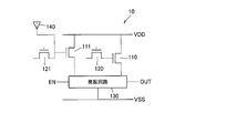
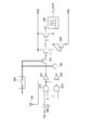
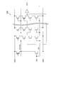
- FIG. 1 is a circuit diagram illustrating a structural example of a semiconductor device according to a first embodiment of the present disclosure.
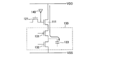
- FIG. 6 is a circuit diagram showing an extracted configuration between the VDD wiring and the VSS wiring of the semiconductor device according to the same embodiment.
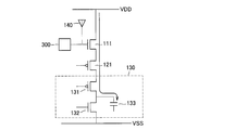
- FIG. 7 is a circuit diagram showing an extracted configuration between a VDD wiring and a VSS wiring of a semiconductor device according to a comparative example. It is a circuit diagram which shows the structural example of the semiconductor device which concerns on a 1st modification. It is a circuit diagram which shows the structural example of the semiconductor device which concerns on a 2nd modification.
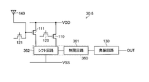
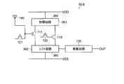
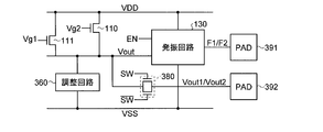
- FIG. 7 is a flowchart showing an example of the operation of the semiconductor device according to the same embodiment. It is a block diagram which shows the structure of the electronic device which concerns on a 1st application example. It is a block diagram which shows the structure of the electronic device which concerns on a 2nd application example. It is a block diagram which shows the structure of the electronic device which concerns on a 3rd application example.
- FIG. 9 is a circuit diagram illustrating a structural example of a semiconductor device according to a second embodiment of the present disclosure.
- 3 is a circuit diagram showing a more specific circuit structure of the semiconductor device according to the same embodiment. It is a circuit diagram which shows the more concrete circuit structure of an oscillation circuit. It is a graph which shows the frequency characteristic of an oscillation circuit. It is a graph which shows the relationship between the input voltage and output voltage in a source follower circuit. It is a figure for demonstrating shift of the voltage range used by the adjustment circuit which concerns on 3rd Embodiment. 9 is a graph showing a relationship between a variation range before and after shifting and a frequency characteristic by the adjustment circuit according to the third embodiment. It is a figure for demonstrating the output voltage from the source follower circuit which concerns on 3rd Embodiment.
- FIG. 11 is a diagram for explaining shift of the output voltage when the ratio of the ON resistance of the P-type transistor and the ON resistance of the N-type transistor in the shift circuit according to the third embodiment is controlled.
- FIG. 11 is a diagram for explaining shift of the output voltage when the ratio of the ON resistance of the P-type transistor and the ON resistance of the N-type transistor in the shift circuit according to the third embodiment is controlled.
- FIGS. 1A to 2C are explanatory views for explaining generation of PID in a plasma process.
- an insulating layer 2 and a conductor layer 3 are formed on a semiconductor substrate 1 in a process using plasma (for example, etching, CVD (Chemical Vapor Deposition), PVD (Physical Vapor Deposition), or sputtering).
- plasma for example, etching, CVD (Chemical Vapor Deposition), PVD (Physical Vapor Deposition), or sputtering.
- the conductor layer 3 Since the conductor layer 3 is in a floating state by the insulating layer 2 and the insulating thin film 2A, the charges of the irradiated cations and electrons are accumulated.
- a current Jin flows from the conductor layer 3 to the semiconductor substrate 1.
- a large current flows through the insulating thin film 2A (corresponding to, for example, a gate insulating film) between the conductor layer 3 and the semiconductor substrate 1, so that the insulating thin film 2A is damaged.
- PID Pulsma (Process) Induced Damage
- the PID causes defects or carrier trap levels inside the insulating thin film 2A or at the interface between the insulating thin film 2A and the semiconductor substrate 1, the threshold voltage Vth of the FET using the insulating thin film 2A as the gate insulating film is changed. And increase the gate leak.
- the wiring layer 4 formed on the conductor layer 3 when the wiring layer 4 formed on the conductor layer 3 is etched by the mask 5, the wiring layer 4 functions as an antenna, so that the wiring layer 4 and the conductor layer 3 can be more exposed. Since electric charges are accumulated, a larger current flows through the insulating thin film 2A. Therefore, in the plasma process when forming the wiring or the via, the influence of the PID becomes larger.
- the threshold voltage Vth of the FET fluctuates and the gate leak increases. Therefore, it may be difficult for the FET affected by the PID to exhibit the designed performance. Therefore, in a semiconductor device, it is important to evaluate the influence of PID on FET.
- FIG. 2A to 2C show an example of a method for evaluating the influence of PID on FET.
- 2A shows the structure of a reference FET
- FIG. 2B shows the structure of a measurement target FET
- FIG. 2C shows the structure of an FET for evaluating the effect of the protection element.
- the influence of the PID on the FET can be evaluated by measuring the threshold voltage Vth and the gate leak of FETs having different influences of the PID and comparing the measured threshold voltage Vth and the gate leak.
- the threshold voltage Vth can be derived from the characteristics of the gate applied voltage and the drain current of the FET.
- the gate leak can be evaluated by measuring the leak current flowing when a voltage is applied between the body, the source and the drain, and the gate at the gate or the body.
- the wiring functioning as an antenna and the via are not connected to the gate via the gate wiring 7A, so it is considered that there is almost no influence from the PID.
- the FET 6B shown in FIG. 2B since the wiring functioning as an antenna and the via 8B are connected to the gate via the gate wiring 7B, it is considered that the threshold voltage Vth varies due to the PID. Therefore, by comparing the threshold voltage Vth of each of the FET 6A and the FET 6B, it is possible to evaluate the variation of the threshold voltage Vth due to the PID.
- the wiring functioning as an antenna and the via 8B are connected to the gate through the gate wiring 7B, and a protection element 9C (for example, a diode or the like) that releases the electric charge of the plasma process is provided. ing. Therefore, in the FET 6C, since the protection element 9C can prevent a large current from flowing into the gate insulating film, it is considered that damage to the gate insulating film by the PID can be avoided. Therefore, by comparing the threshold voltages Vth of the FET 6B and the FET 6C, it is possible to evaluate how much the damage to the gate insulating film due to the PID is mitigated by the protection element 9C.
- a protection element 9C for example, a diode or the like
- the technology according to the present disclosure has been made in view of the above circumstances.
- the technology according to the present disclosure makes it possible to evaluate the influence of PID with higher accuracy by a small-scale measurement circuit provided inside a semiconductor device that executes a predetermined function.
- the technology according to the present disclosure uses an oscillation circuit in which an oscillation frequency fluctuates according to the threshold voltage of the measurement transistor, which is electrically connected to a measurement transistor whose antenna part that functions as an antenna in a plasma process is electrically connected to a gate.
- the effect of PID is to be evaluated in a small-scale circuit by connecting them dynamically.
- the selection transistor electrically measuring the threshold voltage is selected by the selection transistor electrically connected to the gate of the measurement transistor. According to this, it is possible to further increase the influence of the threshold voltage of the measurement transistor on the oscillation frequency of the oscillation circuit, and thus it is possible to evaluate the threshold voltage of the measurement transistor with higher accuracy.
- FIG. 3 is a circuit diagram illustrating a structural example of the semiconductor device according to this embodiment.
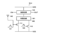
- the semiconductor device 10 includes an antenna section 140, a selection transistor 121, a measurement transistor 111, a reference selection transistor 120, a reference transistor 110, and an oscillation circuit 130.
- the VDD wiring and the VSS wiring supply the semiconductor device 10 with a reference potential.
- the VDD wiring is a wiring having a higher potential than the VSS wiring.
- the VDD wiring is a power wiring
- the VSS wiring is a ground wiring, for example.
- the antenna unit 140 is a structure that functions as an antenna in the plasma process of the manufacturing process of the semiconductor device 10. Specifically, the antenna unit 140 functions as an antenna that collects cations and electrons ionized by plasma in etching, CVD, PVD, sputtering, or the like for processing the semiconductor device 10 using plasma.
- the antenna unit 140 includes wirings that configure the circuit of the semiconductor device 10, interlayer electrodes, through-substrate electrodes (so-called Through-Silicon Via: TSV), inter-chip electrodes (Through-Chip Via: TCV), inter-chip electrode bonding. It may be a structure (so-called CuCu bonding) or a combination thereof.
- the antenna unit 140 electrically connected to the gate of the measurement transistor 111 causes the measurement transistor 111 to generate a PID by the charge accumulated in the antenna unit 140 in the plasma process.
- the influence of the PID is determined by the ratio of the planar area of the gate of the measurement transistor 111 and the antenna section 140 (also referred to as the antenna ratio). Therefore, in the semiconductor device 10, a plurality of measurement transistors 111 whose antenna section 140 is electrically connected to the gate may be provided for each area ratio of the gate of the measurement transistor 111 and the antenna section 140.
- the measurement transistor 111 is a FET, and is provided so that the antenna section 140 is electrically connected to the gate and the oscillation circuit 130 is electrically connected to the source. Specifically, the measurement transistor 111 is provided between the oscillation circuit 130 and the VDD wiring or the VSS wiring. For example, as shown in FIG. 3, the measurement transistor 111 may be provided between the VDD wiring and the oscillation circuit 130. Alternatively, as described later, the measurement transistor 111 may be provided between the VSS wiring and the oscillation circuit 130.
- the threshold voltage Vth varies depending on the PID of the plasma process.
- the channel resistance of the measurement transistor 111 changes, so that the voltage applied to the oscillation circuit 130 can be changed and the oscillation frequency of the oscillation circuit 130 can be changed. Therefore, the measurement transistor 111 can control the oscillation frequency of the oscillation circuit 130 according to the threshold voltage Vth of the measurement transistor 111.
- the measurement transistor 111 When the measurement transistor 111 is provided on the VDD wiring side with respect to the oscillation circuit 130, the measurement transistor 111 can be configured as an N-type transistor. On the other hand, when the measurement transistor 111 is provided on the VSS wiring side with respect to the oscillation circuit 130, the measurement transistor 111 can be configured as a P-type transistor. As a result, the measurement transistor 111 can further increase the fluctuation of the oscillation frequency of the oscillation circuit 130 caused by the fluctuation of the threshold voltage Vth of the measurement transistor 111.
- the selection transistor 121 is an FET and is provided so that the source is electrically connected to the gate of the measurement transistor 111 in parallel with the antenna unit 140.
- the selection transistor 121 switches the transistor electrically connected to the oscillation circuit 130 to the measurement transistor 111 by controlling the on or off state of the measurement transistor 111. Specifically, the selection transistor 121 controls the measurement transistor 111 to be in the ON state, so that the oscillation circuit 130 has a value obtained by subtracting the voltage corresponding to the channel resistance of the measurement transistor 111 from the potential difference between the VDD wiring and the VSS wiring. Control the voltage applied to. At this time, the reference selection transistor 120 is controlled to be in the off state.
- the selection transistor 121 can be provided as a FET of the same conductivity type as the measurement transistor 111. Specifically, when the selection transistor 121 and the measurement transistor 111 are provided on the VDD wiring side with respect to the oscillation circuit 130, the selection transistor 121 can be configured as the same N-type transistor as the measurement transistor 111. On the other hand, when the selection transistor 121 and the measurement transistor 111 are provided on the VSS wiring side with respect to the oscillation circuit 130, the selection transistor 121 can be configured as the same P-type transistor as the measurement transistor 111.
- CMOS complementary MOS
- N-type transistor N-type transistor
- the influence of PID on the measurement transistor 111 may be suppressed.
- the CMOS transfer gate also has a function of a protection element that protects the PID from the antenna unit 140 to the measurement transistor 111. Therefore, by using the selection transistor 121 that does not have the function of the protection element, the influence of the PID is reflected more accurately in the measurement transistor 111, so that the semiconductor device 10 can improve the PID measurement accuracy. .
- the reference transistor 110 is a FET, and is provided so that the oscillation circuit 130 is electrically connected to the source. However, the reference transistor 110 is provided so that the antenna portion 140 is not connected to the gate. Specifically, like the measurement transistor 111, the reference transistor 110 is provided between the oscillator circuit 130 and the VDD wiring or the VSS wiring. For example, as shown in FIG. 3, the reference transistor 110 may be provided between the VDD wiring and the oscillation circuit 130. Alternatively, as described below, the reference transistor 110 may be provided between the VSS wiring and the oscillation circuit 130.
- the reference transistor 110 is different from the measurement transistor 111 in that the wiring or via functioning as an antenna in the plasma process is not electrically connected to the gate. That is, the reference transistor 110 is provided to measure the threshold voltage Vth when there is no influence of PID.
- the reference transistor 110 is provided as an FET similar to the measurement transistor 111 except that the antenna section 140 is not connected to the gate. Specifically, when the reference transistor 110 is provided on the VDD wiring side with respect to the oscillation circuit 130, the reference transistor 110 can be configured as an N-type transistor. On the other hand, when the reference transistor 110 is provided on the VSS wiring side with respect to the oscillation circuit 130, the reference transistor 110 can be configured as a P-type transistor.
- the reference selection transistor 120 is a FET, and is provided so that the source is electrically connected to the gate of the reference transistor 110.
- the reference selection transistor 120 switches the transistor electrically connected to the oscillation circuit 130 to the reference transistor 110 by controlling the on or off state of the reference transistor 110.
- the reference selection transistor 120 controls the voltage applied to the oscillation circuit 130 to a value obtained by subtracting the voltage corresponding to the channel resistance of the reference transistor 110 from the potential difference between the VDD wiring and the VSS wiring. At this time, the selection transistor 121 is controlled to be in the off state.
- the reference selection transistor 120 is provided as a FET of the same conductivity type as the reference transistor 110. Specifically, when the reference selection transistor 120 and the reference transistor 110 are provided on the VDD wiring side with respect to the oscillation circuit 130, the reference selection transistor 120 can be configured as the same N-type transistor as the reference transistor 110. On the other hand, when the reference selection transistor 120 and the reference transistor 110 are provided on the VSS wiring side with respect to the oscillation circuit 130, the reference selection transistor 120 can be configured as the same P-type transistor as the reference transistor 110.
- the oscillation circuit 130 is electrically connected to the source of the measurement transistor 111 or the reference transistor 110 and is provided between the VDD wiring and the VSS wiring.
- the oscillation circuit 130 is an electric circuit that outputs an AC output having an oscillation frequency to the OUT terminal based on the input from the EN terminal.
- the oscillating circuit 130 is a feedback oscillating circuit that causes periodic voltage fluctuations by feeding back a part of the output to the input.
- the oscillator circuit 130 may be a ring oscillator that generates a periodic square wave by feeding back an output, which is an inversion logic such as NOT or NOR connected in an odd number of stages, to the input in a ring shape.
- One of NOT and NOR of the oscillation circuit 130 is replaced with NAND, and the oscillation circuit 130 starts oscillation by inputting a signal instructing oscillation start from the EN terminal to one end of the input of the NAND. To do.
- the oscillator circuit 130 can be formed simultaneously with the other transistors in the same process, and thus an increase in the manufacturing cost of the semiconductor device 10 can be suppressed.
- the oscillation frequency of the oscillation circuit 130 varies depending on the threshold voltage Vth of the electrically connected measurement transistor 111 and reference transistor 110, as described later. Therefore, the semiconductor device 10 compares the oscillation frequency when the reference transistor 110 is electrically connected to the oscillation circuit 130 with the oscillation frequency when the measurement transistor 111 is electrically connected to the oscillation circuit 130. The effect of PID on the measuring transistor 111 can be evaluated.
- FIG. 4 is a circuit diagram showing an extracted configuration between the VDD wiring and the VSS wiring of the semiconductor device 10.
- the antenna section 140 and the selection transistor 121 are connected in parallel to the gate between the VDD wiring and the VSS wiring, and the measurement transistor 111 and one inverter in the oscillation circuit 130 are configured.
- a P-type transistor 131 and an N-type transistor 132 are provided in series.
- a load capacitance 133 is electrically connected to the output side of the inverter.
- the charging time t of the load capacitance 133 is expressed by the following equation (1).
- You can t (R1 + R2) ⁇ C (1)
- the semiconductor device 10 when PID occurs in the measurement transistor 111 and the threshold voltage Vth of the measurement transistor 111 increases, the channel resistance R1 increases, so that the oscillation frequency f of the oscillation circuit 130 may decrease. Recognize. Therefore, by detecting the change in the oscillation frequency f, the semiconductor device 10 can detect whether or not the PID has occurred in the measurement transistor 111. Further, since the oscillation frequency f is inversely proportional to the sum of the channel resistance R1 and the channel resistance R2, the semiconductor device 10 evaluates the variation amount of the channel resistance R1 or the threshold voltage Vth due to the PID from the variation amount of the oscillation frequency f. You can
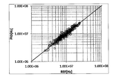
- FIG. 5A and 5B show an example of a PID detection result by the semiconductor device 10.
- the oscillation frequency (expressed as PID) when the measurement transistor 111 is connected to the oscillation circuit 130 is plotted on the vertical axis
- the oscillation frequency when the reference transistor 110 is connected to the oscillation circuit 130 (expressed as REF). ) Is taken on the horizontal axis to compare the two.
- FIG. 5A is a graph showing a detection result when the generation of PID is suppressed by providing a protective element at the gate of the measurement transistor 111
- FIG. 5B intentionally generated PID in the plasma process It is a graph which shows the detection result in a case.
- the oscillation frequency of the oscillation circuit 130 to which the measurement transistor 111 is connected and the oscillation frequency of the oscillation circuit 130 to which the reference transistor 110 is connected are It can be seen that the two are approximately equal to each other.
- the oscillation frequency of the oscillation circuit 130 to which the measurement transistor 111 is connected is higher than that of the oscillation circuit 130 to which the reference transistor 110 is connected. You can see that it is getting smaller.
- the semiconductor device 10 can detect the presence or absence of the PID of the measurement transistor 111 as a change in the oscillation frequency of the oscillation circuit 130.
- FIG. 6 is a circuit diagram illustrating a structural example of a semiconductor device according to a comparative example
- FIG. 7 is a circuit diagram extracting and showing a configuration between a VDD wiring and a VSS wiring of a semiconductor device according to a comparative example. .
- the antenna section 140 is electrically connected to the measurement transistor 111 and the selection transistor 121.
- the semiconductor device 10A in parallel with the measurement transistor 111 and the selection transistor 121, between the VDD wiring or the VSS wiring and the oscillation circuit 130, the reference transistor 110 whose antenna portion is not electrically connected to the gate, and the reference selection.
- the transistor 120 is provided in series.
- a PAD 300 for external input is provided at the gates of the measurement transistor 111 and the reference transistor 110. The input from the PAD 300 controls the measurement transistor 111 and the reference transistor 110 to be in the ON state.
- the electrical connection between the measurement transistor 111 and the oscillation circuit 130 can be controlled by controlling the on / off state of the selection transistor 121.
- the semiconductor device 10A can change the voltage applied to the oscillation circuit 130 according to the threshold voltage Vth of the measurement transistor 111.
- the measurement transistor 111 whose gate is electrically connected to the antenna unit 140 between the VDD wiring and the VSS wiring, the selection transistor 121, and the oscillation circuit.
- a P-type transistor 131 and an N-type transistor 132 forming one inverter in 130 are provided in series.
- a load capacitance 133 is electrically connected to the output side of the inverter.
- the oscillation frequency f of the oscillation circuit 130 can be expressed by the following equation (4).
- the channel resistance R3 of the selection transistor 121 in addition to the channel resistance R1 of the measurement transistor 111 and the channel resistance R2 of the P-type transistor, the channel resistance R3 of the selection transistor 121 also oscillates. It can be seen that the oscillation frequency of the circuit 130 is affected. Therefore, in the semiconductor device 10A, it can be understood that the fluctuation amount of the oscillation frequency with respect to the fluctuation amount of the channel resistance R1 of the measurement transistor 111 is reduced as compared with the semiconductor device 10 according to the present embodiment. Therefore, in the semiconductor device 10A, as compared with the semiconductor device 10 according to the present embodiment, the channel resistance R3 of the selection transistor 121 may cause an error, and the PID detection accuracy may decrease.
- the channel width of the selection transistor 121 in order to reduce the size of the channel resistance R3 of the selection transistor 121 to a negligible level.
- the area occupied by the selection transistor 121 becomes large, so that the area of the semiconductor device 10A becomes large. Since the semiconductor device 10A is provided inside the semiconductor device that performs a predetermined function for the purpose of managing the manufacturing process, it is not preferable that the area of the semiconductor device 10A be large.
- the area of the selection transistor 121, the measurement transistor 111, the P-type transistor 131, and the N-type transistor 132 is S, and the oscillation circuit 130 is configured by 101 stages of inverters, the antenna unit 140 and the wiring are Ignoring the area
- the selection transistor 121 is provided for each of the plurality of measurement transistors 111.
- the semiconductor device 10A according to the comparative example in order to improve the PID detection accuracy, it is necessary to significantly increase the occupied area.
- the semiconductor device 10 according to the present embodiment since the channel resistance of the selection transistor 121 does not affect the oscillation frequency of the oscillation circuit 130, the PID detection accuracy can be improved without significantly increasing the occupied area. Is.
- the selection transistor 121 is provided in parallel with the antenna section 140 on the gate side of the measurement transistor 111 so that the channel resistance R3 of the selection transistor 121 does not affect the oscillation frequency f. be able to. Further, in the semiconductor device 10, since the measurement transistor 111 and the reference transistor 110 are connected in parallel to the same oscillation circuit 130, the semiconductor device 10 can minimize the error factor due to the channel resistance R2 of the P-type transistor 131. it can. Therefore, the semiconductor device 10 can increase the fluctuation amount of the oscillation frequency f with respect to the fluctuation amount of the channel resistance R1 of the measurement transistor 111 without increasing the occupied area, so that the PID detection accuracy can be improved. .
- FIGS. 8A to 8D are circuit diagrams showing structural examples of the semiconductor devices according to the first to fourth modifications.
- a plurality of measurement transistors 211 and 212 whose gates are electrically connected to the antenna units 241 and 242, respectively, and a source each of which is a measurement transistor 211, A plurality of selection transistors 221, 222 electrically connected to the gate of 212, a reference transistor 210, a reference selection transistor 220 whose source is electrically connected to the gate of the reference transistor 210, and a plurality of measurement transistors 211. , 212, and the oscillation circuit 130 electrically connected to the source of the reference transistor 210.
- the antenna part 241 and the measurement transistor 211, and the antenna part 242 and the measurement transistor 212 are provided so that the area ratio (that is, the antenna ratio) between the gate of the measurement transistor and the antenna part is different from each other.
- the semiconductor device 11 according to the first modified example may further include an antenna unit and a measurement transistor having different antenna ratios.
- the measurement transistors 211 and 212, the selection transistors 221, 222, the reference transistor 210, and the reference selection transistor 220 are provided on the VSS wiring side with respect to the oscillation circuit 130. According to this, the semiconductor device 11 can detect the occurrence of the PID even in the FET provided on the VSS wiring side with respect to the oscillation circuit 130.
- the measurement transistors 211 and 212, the selection transistors 221, 222, the reference transistor 210, and the reference selection transistor 220 can be provided as P-type transistors, respectively. According to this configuration, the semiconductor device 11 can further increase the fluctuation of the oscillation frequency of the oscillation circuit 130 caused by the fluctuation of the threshold voltage Vth of the measurement transistors 211 and 212.
- the semiconductor device 12 includes a plurality of measurement transistors 111, 112, 211, 212 whose gates are electrically connected to the antenna portions 141, 142, 241, 242, respectively. , A plurality of selection transistors 121, 122, 221, 222 whose sources are electrically connected to the gates of the measurement transistors 111, 112, 211, 212, reference transistors 110 and 210, and sources whose reference transistors 110, 210, respectively.
- Reference transistors 120 and 220 electrically connected to the gates of the plurality of measurement transistors 111, 112, 211 and 212, and an oscillation circuit 130 electrically connected to the sources of the reference transistors 110 and 210, Equipped with.
- the antenna part 141 and the measurement transistor 111 and the antenna part 142 and the measurement transistor 112 are provided so that the antenna ratios are different from each other, and the antenna part 241 and the measurement transistor 211, and the antenna part 242 and the measurement transistor 212 have the same antenna ratio. Are provided so as to be different from each other.
- the semiconductor device 12 according to the second modification may further include an antenna unit and a measurement transistor having different antenna ratios on the VDD wiring side and the VSS wiring side, respectively.
- the measurement transistors 111 and 112 the selection transistors 121 and 122, the reference transistor 110, and the reference selection transistor 120 are provided on the VDD wiring side with respect to the oscillation circuit 130, and are measured.
- the transistors 211 and 212, the selection transistors 221, 222, the reference transistor 210, and the reference selection transistor 220 are provided on the VSS wiring side with respect to the oscillation circuit 130. According to this, the semiconductor device 12 can detect the presence or absence of PID in the FETs provided on the VDD wiring side and the VSS wiring side of the oscillation circuit 130.
- the semiconductor device 12 can detect the presence or absence of PID of the measurement transistors 111 and 112 on the VDD wiring side by electrically connecting the VDD wiring and the oscillation circuit 130 with a switch (not shown). . Further, the semiconductor device 12 can detect the presence or absence of the PID of the measurement transistors 211 and 212 on the VSS wiring side by electrically connecting the VSS wiring and the oscillation circuit 130 with a switch (not shown).
- the measurement transistors 111 and 112, the selection transistors 121 and 122, the reference transistor 110, and the reference selection transistor 120 provided on the VDD wiring side can be provided as N-type transistors.
- the measurement transistors 211 and 212, the selection transistors 221, 222, the reference transistor 210, and the reference selection transistor 220 provided on the VSS wiring side can be provided as P-type transistors, respectively.
- the semiconductor device 12 can further increase the fluctuation of the oscillation frequency of the oscillation circuit 130 caused by the fluctuation of the threshold voltage Vth of the measurement transistors 111, 112, 211, 212.
- the measurement transistor 111 whose gate is electrically connected to the antenna section 140 and the source are electrically connected to the gate of the measurement transistor 111.
- the protection element 150 is a circuit element that has a high resistance value at a current or voltage within a predetermined range and a low resistance value at a current or voltage above a threshold value.
- the protective element 150 has a low resistance value and can escape the accumulated electric charge. According to this, the protection element 150 can suppress the generation of PID in the measurement transistor 111.
- the protection element 150 may be, for example, various semiconductor diodes.
- the semiconductor device 12 compares the measurement transistor 111 provided with the protection element 150 with the measurement transistor not provided with the protection element 150, so that the PID suppression effect of the protection element 150 can be reduced. Can be evaluated.
- the protective element 150 may be electrically connected to the gate of the measurement transistor 111 by a wiring in a layer above the antenna section 140.
- the protective element 150 is not electrically connected to the measurement transistor 111 in the plasma process in which the antenna unit 140 functions as an antenna. Therefore, in the measurement transistor 111, PID is generated by the antenna unit 140.
- the protection element 150 is electrically connected to the gate of the measurement transistor 111 by a wiring in a layer above the antenna section 140.
- the protective element 150 can suppress the generation of PID using the wiring, the via, or the like in the upper layer of the antenna section 140 as an antenna.
- the protection element 150 can suppress the PID to the measurement transistor 111 due to the via or wiring in the layer above the antenna section 140, and thus the measurement transistor 111 can generate only the PID by the antenna section 140. it can. Therefore, the semiconductor device 13 can evaluate the influence of the PID on the measurement transistor 111 by the antenna unit 140 with higher accuracy.
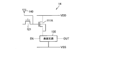
- the measurement transistor 111A whose gate is electrically connected to the antenna section 140 and the source are electrically connected to the gate of the measurement transistor 111.
- the body terminal of the measurement transistor 111A is electrically connected to the source side wiring of the measurement transistor 111A. Normally, the body terminal of the transistor is electrically connected to the VDD wiring or the VSS wiring, but it is also possible to electrically connect to the wiring on the source side of the transistor.
- the semiconductor device 14 according to the fourth modification can detect the presence / absence of a PID by the antenna unit 140 and evaluate the size of the PID for such a measurement transistor 111A as well.
- the measurement transistor 111A is provided on the N-type substrate.
- the measurement transistor 111A is provided on the P-type substrate, a deep well region doped with N-type up to the deep region is formed to prevent a short circuit between the source and the body.
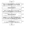
- FIG. 9 is a flowchart showing an example of the operation of the semiconductor device 10 according to this embodiment.
- the reference selection transistor 120 electrically connected to the gate of the reference transistor 110 is controlled to be on, and the selection transistor 121 electrically connected to the gate of the measurement transistor 111 is turned off. It is controlled (S101). As a result, the reference transistor 110 is electrically connected to the oscillation circuit 130.
- the oscillation frequency of the oscillation circuit 130 is measured (S103). Thereby, the oscillation frequency of the oscillation circuit 130 when the transistor in which the PID is not generated is connected is measured.
- the selection transistor 121 electrically connected to the gate of the measurement transistor 111 is controlled to be on, and the reference selection transistor 120 electrically connected to the gate of the reference transistor 110 is controlled to be off (S105). .
- the measurement transistor 111 is electrically connected to the oscillation circuit 130.
- the oscillation frequency of the oscillation circuit 130 is measured (S107). Thereby, the oscillation frequency of the oscillation circuit 130 when the transistor in which the PID is generated is connected is measured.
- the threshold voltage Vth of the measurement transistor 111 changes due to the PID (S111). For example, when the difference between the detected oscillation frequencies is equal to or greater than a predetermined value, the variation in the oscillation frequency may be determined to be due to the variation in the threshold voltage Vth of the measurement transistor 111 due to PID.
- the semiconductor device 10 By using the semiconductor device 10 according to the present embodiment, it is easy to determine whether PID is generated by the antenna unit 140 of the semiconductor device 10 or whether the threshold voltage of the measurement transistor 111 is changed by the PID of the antenna unit 140. Can be determined.
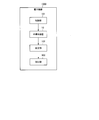
- FIGS. 10 to 12 are block diagrams showing the configurations of electronic devices according to the first to third application examples.
- the electronic device 1000 includes a control unit 101, a semiconductor device 10, a measurement unit 102, and a detection unit 103. It should be noted that some or all of the control unit 101, the measurement unit 102, and the detection unit 103 may be provided inside the semiconductor device 10.
- the control unit 101 controls the on / off state of the selection transistor 121 and the reference selection transistor 120 of the semiconductor device 10 to control the electrical connection between the measurement transistor 111 and the reference transistor 110 and the oscillation circuit 130. .
- the control unit 101 controls the on or off state of the selection transistor 121 of the semiconductor device 10 to electrically connect the plurality of antenna units 140 and the measurement transistor 111 having different antenna ratios to the oscillation circuit 130. To control.
- the semiconductor device 10 outputs an AC output from each of the plurality of measurement transistors 111 having different antenna ratios or the oscillation circuit 130 electrically connected to the reference transistor 110.
- the oscillation frequency of the AC output from the oscillation circuit 130 varies depending on each of the plurality of measurement transistors 111 electrically connected to the oscillation circuit 130 or the channel resistance of the reference transistor 110.
- the semiconductor device 10 can convert the difference in the channel resistance of each of the plurality of measurement transistors 111 having different antenna ratios or the reference transistor 110 into the fluctuation of the oscillation frequency of the oscillation circuit 130.
- the measuring unit 102 measures the oscillation frequency of the AC output from the oscillation circuit 130 of the semiconductor device 10.
- the measurement unit 102 may be a measurement circuit provided inside the semiconductor device 10 or the electronic device 1000, or may be a tester provided outside the electronic device 1000.
- the detection unit 103 detects whether there is a difference between the oscillation frequencies based on the oscillation frequency of the oscillation circuit 130 measured by the measurement unit 102. Specifically, the detection unit 103 compares the oscillation frequency of the oscillation circuit 130 to which the reference transistor 110 is connected with the oscillation frequency of the oscillation circuit 130 to which the measurement transistor 111 is connected. At this time, if the oscillation frequency of the oscillation circuit 130 to which the measurement transistor 111 is connected fluctuates from the oscillation frequency of the oscillation circuit 130 to which the reference transistor 110 is connected, the detection unit 103 detects that there is a difference in the oscillation frequencies. . The detection unit 103 may also detect that a PID has occurred in the electronic device 1000.
- the semiconductor device 10 can detect whether or not the PID is generated in the internal transistor with a smaller area and a smaller number of terminals. Therefore, the semiconductor device 10 can reduce the process management cost of the electronic device 1000 according to the first application example.
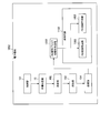
- an electronic device 1001 As shown in FIG. 11, an electronic device 1001 according to the second application example includes a control unit 101, a semiconductor device 10, a measurement unit 102, a detection unit 103, a processing unit 104, and a reference voltage control circuit 1201. A reference voltage generation circuit 1301 and a main body circuit 1101 are provided. It should be noted that some or all of the control unit 101, the measurement unit 102, and the detection unit 103 may be provided inside the semiconductor device 10.
- control unit 101 the semiconductor device 10, the measurement unit 102, and the detection unit 103 are the same as those described in the first application example, so description thereof will be omitted here.
- the processing unit 104 determines a process for suppressing the influence of the generated PID based on the presence or absence of the PID.
- the processing unit 104 outputs an instruction to increase the reference voltage supplied to the main body circuit 1101 that executes the function of the electronic device 1001.
- the threshold voltage Vth of the transistor rises. Therefore, at the design reference voltage of the electronic device 1001, the transistor may not be controlled to be in the ON state, or the current flowing through the transistor may decrease. There is. Therefore, the processing unit 104 instructs the processing for increasing the reference voltage supplied to the main body circuit 1101 so that the main body circuit 1101 can be driven as in the case where the PID did not occur.
- the reference voltage control circuit 1201 controls the reference voltage generated by the reference voltage generation circuit 1301 based on the instruction from the processing unit 104. Specifically, the reference voltage control circuit 1201 controls the reference voltage generation circuit 1301 so as to increase the reference voltage supplied to the main body circuit 1101 based on the instruction of the processing unit 104. For example, the reference voltage control circuit 1201 may control the reference voltage generation circuit 1301 to raise the reference voltage by using a fuse or trimming.
- the reference voltage generation circuit 1301 generates a reference voltage supplied to the main body circuit 1101.
- the reference voltage generation circuit 1301 is a power supply circuit that generates a reference voltage having a voltage value based on the control of the reference voltage control circuit 1201.
- the reference voltage generation circuit 1301 may generate a boosted reference voltage based on the control of the reference voltage control circuit 1201 so as to cancel the fluctuation of the threshold voltage Vth of the transistor due to the PID.
- the main body circuit 1101 is a main circuit that is driven by the reference voltage supplied from the reference voltage generation circuit 1301 and executes the function of the electronic device 1001. Since the voltage value of the reference voltage supplied from the reference voltage generation circuit 1301 is controlled based on the presence / absence of PID, the main body circuit 1101 can be smoothly driven regardless of the presence / absence of PID.
- an electronic device 1002 includes a control unit 101, a semiconductor device 10, a measurement unit 102, a detection unit 103, a processing unit 104, and a PID resistant block switching control circuit. 1202 and a main body circuit 1102 including a PID low withstand circuit 1302 and a PID high withstand circuit 1402. It should be noted that some or all of the control unit 101, the measurement unit 102, and the detection unit 103 may be provided inside the semiconductor device 10.
- control unit 101 the semiconductor device 10, the measurement unit 102, and the detection unit 103 are the same as those described in the first application example, so description thereof will be omitted here.
- the processing unit 104 determines a process for suppressing the influence of the generated PID based on the presence or absence of the PID.
- the processing unit 104 outputs an instruction to switch the function executed by the PID low tolerance circuit 1302 in the main body circuit 1102 so that the PID high tolerance circuit 1402 executes. To do.
- the threshold voltage Vth of the transistor rises. Therefore, at the reference voltage when the electronic device 1002 is designed, the transistor may not be controlled to be in the ON state or the current flowing through the transistor may decrease. There is.
- the processing unit 104 instructs the main circuit 1102 to switch the circuits so that the PID high withstand circuit 1402 that is not easily influenced by the PID is used instead of the PID low withstand circuit 1302 that is greatly influenced by the PID. To do.
- the PID resistant block switching control circuit 1202 controls switching of the connection between the PID low resistant circuit 1302 and the PID high resistant circuit 1402 in the main body circuit 1102 based on an instruction from the processing unit 104. Specifically, the PID resistant block switching control circuit 1202 switches the circuit connection from the PID low resistant circuit 1302 to the PID high resistant circuit 1402 based on an instruction from the processing unit 104. For example, the PID resistant block switching control circuit 1202 may switch the connection with the circuit in the main body circuit 1102 from the PID low resistant circuit 1302 to the PID high resistant circuit 1402 by using a fuse or a switching element.
- the main body circuit 1102 is a main circuit that executes the function of the electronic device 1001, and includes a PID low tolerance circuit 1302 and a PID high tolerance circuit 1402.
- the PID low tolerance circuit 1302 and the PID high tolerance circuit 1402 are a group of circuits that execute the same function, and which one is used is switched depending on the presence or absence of PID. Specifically, in the main body circuit 1102, the PID low tolerance circuit 1302 is used when the PID is not generated, and the PID high tolerance circuit 1402 is used when the PID is generated. According to this, the main body circuit 1102 can be smoothly driven regardless of the presence or absence of the PID.
- FIG. 13 is a circuit diagram illustrating a structural example of the semiconductor device according to this embodiment.
- the semiconductor device 20 includes an antenna section 140, a selection transistor 121, a measurement transistor 111, a reference selection transistor 120, a reference transistor 110, a load element 250, and an oscillator. And a circuit 230.
- the sources of the measurement transistor 111 and the reference transistor 110 are electrically connected to the input of the oscillation circuit 230 and the load element 250, as compared with the semiconductor device 10 according to the first embodiment. The difference is that they are connected.
- the load element 250 is an element that consumes power and is provided to control the voltage input to the oscillation circuit 230.
- the load element 250 is a passive element having a predetermined resistance, and is provided between the sources of the measurement transistor 111 and the reference transistor 110 and the VSS wiring (or the ground wiring).
- the load element 250 may be any passive element having a predetermined resistance, and may be, for example, a resistance element or a load transistor.
- the oscillating circuit 230 is a voltage controlled oscillating circuit capable of controlling the oscillating frequency according to the magnitude of the input voltage.
- the oscillator circuit 230 may be, for example, a voltage-controlled ring oscillator.
- the potential difference between the VDD wiring and the VSS wiring is divided based on the channel resistance of the measurement transistor 111 or the reference transistor 110 and the resistance value of the load element 250, A voltage according to the channel resistance of the measurement transistor 111 or the reference transistor 110 is input to the oscillation circuit 230. That is, in the semiconductor device 20, by connecting the load element 250 having a predetermined resistance and the oscillation circuit 230 in parallel, the voltage based on the fluctuation of the channel resistance of the measurement transistor 111 can be input to the oscillation circuit 230. it can. According to this, in the semiconductor device 20, the fluctuation of the channel resistance of the measurement transistor 111 can be detected as the fluctuation of the oscillation frequency of the oscillation circuit 230.
- the oscillation circuit 130 since the potential difference between the VDD wiring and the VSS wiring is shared by the measurement transistor 111 and the oscillation circuit 130, when the potential difference between the VDD wiring and the VSS wiring is small, The voltage applied to the oscillator circuit 130 becomes too small. In such a case, the oscillation circuit 130 becomes difficult to oscillate. In order to increase the oscillation frequency of the oscillator circuit 130, it is conceivable to simplify the configuration of the oscillator circuit 130 (for example, reduce the number of inverters in the ring oscillator). In such a case, the oscillator circuit is The accuracy of 130 is reduced.
- the oscillation circuit 130 when the oscillation circuit 130 starts to oscillate, power is consumed in the oscillation circuit 130 due to the parasitic capacitance, so that the voltage applied to the oscillation circuit 130 gradually increases. Become.
- the voltage applied to the oscillation circuit 130 stabilizes, and it takes time until the oscillation frequency of the oscillation circuit 130 stabilizes. Therefore, it takes time to detect the presence or absence of the PID. It will cost you.
- the oscillation frequency of the oscillation circuit 230 is controlled by the input voltage, it is possible to apply the entire potential difference between the VDD wiring and the VSS wiring to the oscillation circuit 230. it can.
- the voltage input to the oscillation circuit 230 is determined by the channel resistance of the measurement transistor 111 or the reference transistor 110 and the resistance value of the load element 250. This shortens the time until the voltage input to the oscillation circuit 230 stabilizes, and thus the semiconductor device 20 can shorten the time required to detect the presence or absence of the PID.
- FIG. 14 is a circuit diagram showing a more specific circuit structure of the semiconductor device 20 according to the present embodiment
- FIG. 15 is a circuit diagram showing a more specific circuit structure of the oscillator circuit 230.
- the semiconductor device 20 includes a measurement transistor 111 whose gate is electrically connected to the antenna unit 140, and a reference transistor 110 whose gate is not electrically connected to the antenna unit 140. .
- the sources of the measurement transistor 111 and the reference transistor 110 are connected in parallel to a load element 250 composed of a load transistor and an oscillation circuit 230 which is a voltage controlled ring oscillator. As a result, the potential difference between the VDD wiring and the VSS wiring is applied to the oscillation circuit 230. Further, since the divided voltage corresponding to the channel resistance of the measurement transistor 111 or the reference transistor 110 is input to the oscillation circuit 230, an alternating current having an oscillation frequency corresponding to the channel resistance is output.
- the oscillator circuit 230 may have a circuit structure as shown in FIG.
- the oscillator circuit 230 is, for example, a ring oscillator in which NOT gates (inverters) are connected in an odd number of stages (for example, 101 stages) in a ring shape.
- the oscillator circuit 230 uses the N-type transistor and the P-type transistor complementarily to apply a potential difference based on the potential difference Vd between the VDD wiring and the VSS wiring and the input voltage Vin to each of the internal NOT gates. can do. Thereby, the oscillation circuit 230 can control the oscillation frequency of the AC output based on the magnitude of the input voltage.
- the selection transistor 121 and the reference selection transistor 120 are electrically connected to the gates of the measurement transistor 111 and the reference transistor 110, respectively.
- a common switch 260 is electrically connected to the gates of the selection transistor 121 and the reference selection transistor 120, and the gates of the selection transistor 121 and the reference selection transistor 120 are electrically connected to another power supply via the switch 260. To be done.
- a logic circuit including NOT gates (inverters) 281, 280 and NAND gates 271, 270 is electrically connected to the sources or drains of the selection transistor 121 and the reference selection transistor 120.
- the logic circuit including the NOT gates 281, 280 and the NAND gates 271, 270 turns on the measurement transistor 111 via the selection transistor 121. Control the state. Further, when the PID_SEL terminal is L (Low) and the EN terminal is H (High), the logic circuit controls the reference transistor 110 to the ON state via the reference selection transistor 120. Further, when the EN terminal is L (Low), the logic circuit controls the measurement transistor 111 and the reference transistor 110 to be in the off state regardless of whether the PID_SEL terminal is H (High) or L (Low).
- the semiconductor device 20 it is possible to detect the presence or absence of PID with high accuracy even when the power supply voltage is low. Further, according to the semiconductor device 20, it is possible to detect the presence or absence of the PID in a shorter time.
- the semiconductor device 20 according to the second embodiment is different from the semiconductor device 10 according to the first embodiment in that the sources of the measurement transistor 111 and the reference transistor 110 are electrically connected to the input of the load element 250 and the oscillation circuit 230. The difference is that it is connected to. Therefore, each of the modification and application of the semiconductor device 10 described in the first embodiment can be similarly applied to the semiconductor device 20 according to the second embodiment.
- the variation amount of the channel resistance R1 or the threshold voltage Vth due to the PID can be calculated by a simpler method. Is possible.
- the source formed by the measurement transistor 111 and the reference transistor 110 is used so as to use a linear region (also referred to as a region that can be linearly approximated) in the frequency characteristic of the oscillation circuit 130. It is necessary to process the voltage obtained from the follower circuit.
- a semiconductor device a detection method, an electronic device, and a control method for the electronic device, which can realize a simpler method of converting the oscillation frequency f into a voltage value, will be described below with examples.
- a circuit that processes a voltage in a region where linear approximation is possible will be referred to as an “adjustment circuit”.
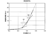
- FIG. 16 is a graph showing the frequency characteristic of the oscillation circuit.
- the oscillation frequency exponentially increases in response to an increase in applied voltage in a region where the voltage value is low (for example, a region below 0.4 V in FIG. 16).
- the oscillation frequency rises while maintaining an approximately constant slope with respect to the increase in the applied voltage.
- the linearity between the applied voltage and the oscillation frequency collapses, and the oscillation occurs in response to the increase in the applied voltage.
- the frequency approaches the upper limit.
- the manufacturing variation (also referred to as ⁇ Vth) of the threshold voltage Vth of the transistor formed in the semiconductor device is 20 mV and the shift amount (also referred to as PID) of the threshold voltage Vth due to the PID is 50 mV.
- the range Q1 of variations in the threshold voltage Vth of the transistors included in the device, that is, the voltage range Q1 used is 70 mV.
- the oscillation frequency f of the oscillation circuit 130 is specified by multiplying the voltage Vin input to the source follower circuit by a fixed coefficient. I can't.
- the fluctuation range of the output voltage Vout from the source follower circuit is narrowed by using the adjustment circuit.
- the linearity of the oscillation frequency f with respect to the voltage input to the oscillation circuit 130 (that is, the output voltage Vout from the source follower circuit) is increased. Therefore, the oscillation is performed by multiplying the input voltage Vin by a fixed coefficient. It is possible to specify the oscillation frequency f of the circuit 130.
- the linearity of the oscillation frequency f with respect to the output voltage Vout is increased by narrowing the voltage range Q1 to be used to 35 mV, which is half of 70 mV. Therefore, the oscillation frequency obtained by multiplying the input voltage Vin by a coefficient. It is possible to improve the accuracy of f.
- the adjustment circuit according to the present embodiment can also have a function of shifting the variation range of the output voltage Vout from the source follower circuit.
- the oscillation circuit 130 is obtained. It is possible to more accurately specify the oscillation frequency f of the input voltage Vin.
- the adjustment circuit according to the present embodiment has the roles of limiting the variation range of the output voltage Vout from the source follower circuit and shifting the variation range of the output voltage Vout to a desired range. be able to.
- limiting the variation range of the output voltage Vout means adjusting the voltage sensitivity of the source follower circuit. That is, as indicated by a straight line L11 in FIG. 17, the slope of the output voltage Vout output from the source follower circuit is normally proportional to the input voltage Vin to the gate of the transistor forming the source follower circuit. Note that FIG. 17 is a graph showing the relationship between the input voltage and the output voltage in the source follower circuit.
- the voltage sensitivity of the source follower circuit is adjusted by providing an adjustment circuit.
- the voltage sensitivity of the source follower circuit is adjusted so that the slope of the output voltage Vout with respect to the input voltage Vin is half the slope of the straight line L11 (corresponding to the straight line L12).
- the fluctuation range of the output voltage Vout with respect to the fluctuation range ( ⁇ Vth + PID) of the input voltage Vin can be reduced to a fluctuation range Q12 that is half the original fluctuation range Q11. Therefore, the input voltage Vin is multiplied by a coefficient. This makes it possible to increase the accuracy of the oscillation frequency f obtained.
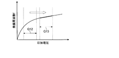
- FIG. 18 is a diagram for explaining the shift of the voltage range used by the adjustment circuit according to the present embodiment
- FIG. 19 is a relationship between the variation range before and after the shift and the frequency characteristic by the adjustment circuit according to the present embodiment. It is a graph which shows.
- the linearity of the frequency characteristic of the voltage (output voltage Vout) input to the oscillation circuit 130 is secured. It becomes possible to shift to the variation range Q13 within the region. Thereby, the oscillation frequency f of the oscillation circuit 130 can be specified more accurately from the input voltage Vin.
- the adjustment circuit according to the present embodiment does not need to have both the function of limiting the voltage fluctuation range of the source follower circuit and the function of shifting the voltage range to be used, and may have either function. Good.
- the present invention is not limited to this, and the high voltage region It is also possible to design the adjustment circuit so as to shift the fluctuation range within (for example, a region larger than the predetermined voltage value referred to in the description of FIG. 16) to the low voltage side.
- FIG. 20 is a diagram for explaining the output voltage from the source follower circuit.
- the gate-source voltage Vgs of the reference transistor 110 / measurement transistor 111 is a voltage obtained by subtracting the output voltage Vout0 from the input voltage Vin, as shown in the following equation (9).
- the drain-source voltage Vds of the reference transistor 110 / measurement transistor 111 is a voltage obtained by subtracting the output voltage Vout0 from the power supply voltage VDD as shown in the following expression (10).
- the voltage obtained by subtracting the threshold voltage Vth of the reference transistor 110 / measurement transistor 111 and the drain-source voltage Vds from the gate-source voltage Vgs is less than zero is the following: As shown in Expression (11), the voltage obtained by subtracting the threshold voltage Vth and the power supply voltage VDD from the input voltage Vin needs to be less than zero.
- the current Ids1 flowing between the drain and the source of the reference transistor 110 / measurement transistor 111 can be obtained from the following equation (12).
- ⁇ 1 is the gain of the reference transistor 110 / measurement transistor 111.
- the output voltage Vout0 can be obtained by the following equation (13).
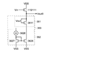
- FIG. 21 is a circuit diagram showing a schematic configuration example of the adjustment circuit according to the first specific example of the present embodiment.
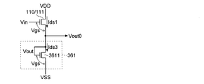
- the adjusting circuit is configured using the limiting circuit 361 that limits the variation range of the output voltage Vout0 will be described as an example.
- the limiting circuit 361 includes a load transistor 3611 whose gate and drain are short-circuited.
- the drain and gate of the load transistor 3611 are connected to the sources of the reference transistor 110 and the measurement transistor 111, and the sources are connected to the ground voltage VSS.
- the saturation condition of the load transistor 3611 is expressed by the following equation (14).
- a current Ids1 flowing between the drain and source of the reference transistor 110 / measurement transistor 111 is obtained from the following equation (15)
- a current Ids3 flowing between the drain and source of the load transistor 3611 is obtained by the following equation (16). Required from.
- the output voltage Vout0 is reduced to about 1/2 as compared with the example shown in FIG. 20, as represented by the following formula (18). This indicates that the variation range of the output voltage Vout0 is limited to approximately half.
- the output voltage Vout0 is input to the oscillator circuit 130.
- FIG. 22 is a circuit diagram showing a schematic configuration example of the adjustment circuit according to the second specific example of the present embodiment.
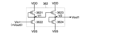
- the adjustment circuit is configured using the shift circuit 362 that shifts the variation range of the output voltage Vout will be described as an example.
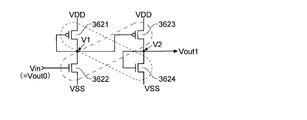
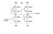
- the shift circuit 362 includes a P-type first transistor 3621 and an N-type second transistor 3622 which are connected in series, and a P-type first transistor 3621 which is also connected in series.
- the three-transistor 3623 and the N-type fourth transistor 3624 are connected in parallel between the power supply voltage VDD and the ground voltage VSS.
- the shift circuit 362 has a configuration in which two CMOS (Complementary Metal-Oxide-Semiconductor) circuits (hereinafter, referred to as CMOS analog inverting circuits) each including a P-type transistor and an N-type transistor connected in series are connected in series.
- CMOS Complementary Metal-Oxide-Semiconductor
- the drains of the first transistor 3621 and the second transistor 3622 are connected to each other.
- the drains of the third transistor 3623 and the fourth transistor 3624 are connected to each other.
- the output voltage Vout from the source follower circuit is applied to the gate of the second transistor 3622.
- the gate of the first transistor 3621 is connected to the drain of the first transistor 3621 and the drain of the second transistor 3622 as well as to the gate of the third transistor 3623.
- the drain of the third transistor 3623 and the drain of the fourth transistor 3624 are connected to the gate of the fourth transistor 3624 and also to a circuit in the subsequent stage (for example, the limiting circuit 361 (or the oscillation circuit 130)).
- the on-resistance of the P-type transistor (the first transistor 3621 or the third transistor 3623) and the N-type transistor (the second transistor 3622 or the fourth transistor 3624) connected in series are used. It is possible to control the voltage value of the voltage output to the subsequent stage by controlling the ratio with the on resistance of the.
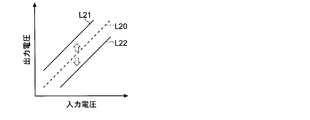
- FIG. 23 is a diagram for explaining the shift of the output voltage when the ratio of the ON resistance of the P-type transistor and the ON resistance of the N-type transistor in the shift circuit is controlled.
- a broken line L20 indicates that the ON resistance of the P-type transistor (the first transistor 3621 or the third transistor 3623) and the ON resistance of the N-type transistor (the second transistor 3622 or the fourth transistor 3624) have the same resistance value.
- the voltage value of the voltage V1 or V2 (corresponding to the output voltage Vout1 from the shift circuit 362) output to the subsequent stage is shown.
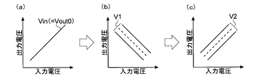
- the CMOS analog inversion circuit composed of the P-type transistor and the N-type transistor connected in series is formed as one stage or an odd number stage, as shown in (a) and (b) of FIG.
- the voltage (for example, the voltage V1 in the examples shown in FIGS. 22 and 24) output to the output terminal has a voltage value inverted with respect to the input voltage Vin. Therefore, in the present embodiment, the CMOS analog inversion circuit composed of the P-type transistor and the N-type transistor has two stages or even stages, so that the output voltage can be changed as shown in (c) of FIG. Are again inverted (in the example shown in FIGS. 22 and 24, for example, voltage V2).
- the voltage value of the output voltage Vout1 is increased, and when the oscillation frequency f is desired to be decreased, the voltage value of the output voltage Vout1 is reduced.
- the on-resistances of the second transistor 3622 and the third transistor 3623 which are diagonally located are decreased. At that time, the on resistances of the first transistor 3621 and the fourth transistor 3624 which are diagonally opposite to each other may be increased.
- the on resistance of the second transistor 3622 and the third transistor 3623 is increased. At that time, on-resistances of the first transistor 3621 and the fourth transistor 3624 may be reduced.
- a method of adjusting the gate length (L length) or gate width (W length) of each transistor, or adjusting the number of Fingers of each transistor may be adopted.
- FIG. 26 is a circuit diagram showing a schematic configuration example of the shift circuit 362 when the number of Fingers of each of the first to fourth transistors 3621 to 3624 is 2.
- the first transistor 3621 includes two transistors 3621a and 3621b
- the second transistor 3622 includes two transistors 3622a and 3622b
- the third transistor 3623 includes two transistors 3623a and 3623b.
- the fourth transistor 3624 is composed of two transistors 3624a and 3624b.
- FIG. 27 is a graph showing an example of the output voltage output from the shift circuit when the number of Fingers of each of the first to fourth transistors is switched.
- broken lines ⁇ 0 indicate the case where the number of Fingers of each of the first to fourth transistors 3621 to 3624 is 1.
- a curve P1 shows a case where the total number of fingers of the second transistor 3622 and the third transistor 3623 is 3, and a total number of fingers of the first transistor 3621 and the fourth transistor 3624 is 2, and the curve P2 is A case where the total number of Fingers of the second transistor 3622 and the third transistor 3623 is 3 and the total number of Fingers of the first transistor 3621 and the fourth transistor 3624 is 1 is shown, and the curve P3 shows the second transistor 3622 and the third transistor 3622.
- a curve P4 indicates a total number of fingers of the second transistor 3622 and the third transistor 3623. Finger Was a 4 shows a case where the total Finger number of the first transistor 3621 and the fourth transistor 3624 is 1.
- the curve M1 shows a case where the total number of fingers of the second transistor 3622 and the third transistor 3623 is 2, and the total number of fingers of the first transistor 3621 and the fourth transistor 3624 is 3, and the curve M2 is A case where the total number of fingers of the second transistor 3622 and the third transistor 3623 is 1 and the total number of fingers of the first transistor 3621 and the fourth transistor 3624 is 3 is shown, and the curve M3 shows the second transistor 3622 and the third transistor 3622. The case where the total number of fingers of the three-transistor 3623 is 2 and the total number of fingers of the first transistor 3621 and the fourth transistor 3624 is 4 is shown, and the curve M4 indicates the total number of fingers of the second transistor 3622 and the third transistor 3623. Finge The number is 1, which shows the case of the first transistor 3621 and the total Finger number 4 of the fourth transistor 3624.
- FIG. 28 is a circuit diagram showing a schematic configuration example of the adjustment circuit according to the third specific example of the present embodiment.
- the adjustment circuit 360 according to the third specific example has a configuration in which a limiting circuit 361 and a shift circuit 362 are connected in series to a source follower circuit configured by the measurement transistor 111 and the reference transistor 110. May have.
- the shift circuit 362 may be formed of a resistance element 3625.
- the output voltage Vout0 can be shifted to the high voltage side. Note that when the output voltage is shifted from Vout0 to the low voltage side, the resistance element 3625 may be provided on the drain side of the source follower circuit.
- FIG. 29 is a circuit diagram showing a schematic configuration example of the adjustment circuit according to the fourth specific example of the present embodiment.
- the shift circuit 362 has two transistors 3626 and 3627 and a constant current circuit 3628. And a configuration replaced with a circuit configuration including.
- the two transistors 3626 and 3627 form a current mirror circuit by connecting their gates to the drain of one transistor 3627.
- the drain of the transistor 3627 is connected to the constant current circuit 3628.
- one transistor 3626 forming the current mirror circuit functions so as to limit the current flowing in the source follower circuit. Therefore, by controlling the current flowing through the constant current circuit 3628, the output voltage Vout0 can be shifted to the high voltage side.
- the shift circuit 362 may be provided on the drain side of the source follower circuit.
- the output voltage Vout0 can also be shifted by adjusting the ratio of the ON resistances of the measurement transistor 111 or the reference transistor 110 and the load transistor 3611.
- a method of adjusting the gate length (L length) or gate width (W length) of each transistor or adjusting the number of fingers of each transistor may be adopted. .
- the limiting circuit 361 and the shift circuit 362 may be the same as the limiting circuit 361 and the shift circuit 362 illustrated in the description of the adjustment circuit 360 described above.
- FIG. 30 is a circuit diagram illustrating a structural example of the semiconductor device according to the first example of the present embodiment.
- the semiconductor device 30-1 according to the first example has, for example, the same configuration as the semiconductor device 10 described in the first embodiment with reference to FIG. 3 and has a measurement transistor 111 and a reference transistor 110. Is provided with an adjusting circuit 360 including a limiting circuit 361 on the source side of the source follower circuit.
- FIG. 31 is a circuit diagram illustrating a structural example of the semiconductor device according to the second example of the present embodiment.
- the adjusting circuit 360 including the limiting circuit 361 is connected to the oscillation circuit 130 and the ground.
- a structure provided between the voltage VSS and the voltage VSS is provided.
- FIG. 32 is a circuit diagram illustrating a structural example of the semiconductor device according to the third example of the present embodiment.
- the adjustment circuit 360 including the limiting circuit 361 has the drain of the source follower circuit.
- the structure provided on the side is provided.
- FIG. 33 is a circuit diagram illustrating a structural example of the semiconductor device according to the fourth example of the present embodiment.
- the oscillation circuit 130 is provided between the adjustment circuit 360 and the power supply voltage VDD.
- FIG. 34 is a circuit diagram illustrating a structural example of the semiconductor device according to the fifth example of the present embodiment.
- the semiconductor device 30-5 according to the fifth example has, for example, the same configuration as the semiconductor device 10 described with reference to FIG. 3 in the first embodiment and has a measurement transistor 111 and a reference transistor 110.
- the shift circuit 362 is connected to the source side of the source follower circuit configured by and the limiting circuit 361 is connected to the output of the shift circuit 362.
- FIG. 35 is a circuit diagram illustrating a structural example of the semiconductor device according to the sixth example of the present embodiment.
- the limiting circuit 361 is connected to the drain side of the source follower circuit, It has a structure in which the oscillation circuit 130 is connected to the output of the shift circuit 362.
- the present invention is not limited to this. That is, in the present embodiment, the measurement transistor 111 and the reference transistor 110 can be configured by P-type transistors. In that case, for example, in the structures described in the first to sixth examples, the power supply voltage VDD and the ground voltage VSS are exchanged.
- FIG. 36 is a diagram showing a circuit configuration of a semiconductor device used for executing this demonstration experiment.
- FIG. 37 is a graph showing the results obtained by this demonstration experiment.
- the adjustment circuit 360 is provided on the source side of the source follower circuit configured by the measurement transistor 111 and the reference transistor 110 was used.
- the adjusting circuit 360 the limiting circuit 361 according to the first specific example described with reference to FIG. 21 is used.
- the output voltage Vout output from the source follower circuit is input to the oscillation circuit 130.
- the oscillation frequency of the oscillation circuit 130 was measured via the output pad 391.
- a ring oscillator is used as the oscillator circuit 130.
- the output of the source follower circuit was branched and connected to the output pad 392 via the switch 380.
- the switch 380 is turned on with the enable signal EN input to the oscillation circuit 130 turned off, so that the source follower circuit when the voltage Vg1 is applied to the measurement transistor 111 is turned on. From the source follower circuit when the voltage Vg2 is applied to the reference transistor 110 (the output voltage Vout1 is referred to as the output voltage Vout1). It was measured directly via. Further, in this experiment, by turning on the state enable signal EN with the switch 380 turned off, the oscillation frequency F1 of the oscillation circuit 130 when the voltage Vg1 is applied to the measurement transistor 111 and the voltage Vg2 to the reference transistor 110 are set. The oscillation frequency F2 of the oscillation circuit 130 when applied was also measured via the output pad 391.
- the broken line plots the value obtained by subtracting the oscillation frequency F1 from the oscillation frequency F2 and multiplying by a predetermined proportional multiplier
- the solid line plots the value obtained by subtracting the output voltage Vout1 from the output voltage Vout2. It is a thing. As can be seen from FIG. 37, the value obtained by subtracting the oscillation frequency F1 from the oscillation frequency F2 and multiplying it by a predetermined proportional multiplier and the value obtained by subtracting the output voltage Vout1 from the output voltage Vout2 are substantially the same. This indicates that the variation of the output voltage Vout can be obtained by multiplying the frequency difference by a predetermined proportional multiplier.
- the output voltage Vout2 when the voltage Vg2 is applied to the reference transistor 110 can be obtained by the following equation (19), and the output voltage Vout1 when the voltage Vg1 is applied to the measurement transistor 111 is obtained by the following equation (20). be able to.
- the design value of the threshold voltage of each transistor is Vth
- the variation of the threshold voltage Vth1 of the measurement transistor 111 is ⁇ Vth1
- the variation of the threshold voltage Vth2 of the reference transistor 110 is ⁇ Vth2
- the threshold voltage Vth1 due to damage from the antenna is
- the shift amount is ⁇ PID
- the threshold voltage Vth2 of the reference transistor 110 is expressed by the following equation (21)
- the threshold voltage Vth1 of the measurement transistor 111 is expressed by the following equation (22).
- the output voltage Vout is input to the oscillation circuit 130 and converted into the oscillation frequency f.
- the oscillation frequency f at the output voltage Vout2 is F2
- the oscillation frequency f at the output voltage Vout1 is F1. Further, the oscillation frequency f can be changed to a voltage value by the function G (f) as shown in the following equations (24) and (25).
- the threshold voltages Vth1 and Vth2 can be approximated by the following equation (26). it can.
- the difference between the threshold voltage Vth2 of the reference transistor 110 and the threshold voltage Vth1 of the measurement transistor 111, that is, the shift amount ⁇ PID of the threshold voltage Vth1 due to damage from the antenna can be obtained by the following equation (27). Is.
- mismatch component ( ⁇ Vth1- ⁇ Vth2) remains in the equation (27), since this mismatch component is a completely random value, it is possible to measure a sufficient number of samples and take the average thereof. , Can be reduced to a negligible level.
- FIG. 38 is a graph showing an example of the voltage value of the mismatch component when the antenna is damaged and when it is not damaged.
- the black circles indicate the threshold voltage Vth when the antenna is not damaged
- the white circles indicate the threshold voltage when the antenna is damaged.
- the average value of the threshold voltage Vth was ⁇ 0.0004 [V] when the antenna was not damaged, whereas the threshold value Vth was the threshold value when the antenna was damaged.
- the average value of the voltage Vth was 0.039 [V]. This indicates that the threshold voltage Vth of the measurement transistor 111 is shifted by 0.039 V on average due to damage from the antenna.
- the semiconductor device, the detection method, the electronic device, and the semiconductor device capable of calculating the variation amount of the channel resistance R1 or the threshold voltage Vth due to the PID by the simple method using the linear approximation.
- An electronic device control method is realized.
- the effects described in the present specification are merely explanatory or exemplifying ones, and are not limiting. That is, the technique according to the present disclosure may have other effects that are apparent to those skilled in the art from the description of the present specification, in addition to or instead of the above effects.
- At least one or more measurement transistors whose antenna part that functions as an antenna in the plasma process is electrically connected to the gate;
- a selection transistor in which a source is electrically connected in parallel to the antenna unit to the gate of the measurement transistor,
- An oscillation circuit electrically connected to the source of the measurement transistor, the oscillation frequency of which varies depending on the threshold voltage of the measurement transistor,
- a semiconductor device comprising: (2) The oscillation circuit is provided between the VDD wiring and the VSS wiring, The semiconductor device according to (1), wherein the measurement transistor is provided between the oscillation circuit and the VDD wiring or the VSS wiring. (3) The semiconductor device according to (2), wherein the oscillation circuit is a ring oscillator.
- the oscillating circuit is an oscillating circuit in which an output oscillating frequency varies depending on an input voltage
- the measurement transistor and the selection transistor are transistors of the same conductivity type.
- a plurality of the measurement transistors are provided, The measurement transistor provided on the VDD wiring side of the oscillation circuit is an N-type transistor, and the measurement transistor provided on the VSS wiring side of the oscillation circuit is a P-type transistor.
- a plurality of the measurement transistors are provided, The semiconductor device according to any one of (1) to (7), wherein the area ratios of the antenna section and the gate are different from each other in each of the plurality of measurement transistors. (9) The semiconductor device according to any one of (1) to (8), wherein a protective element is further electrically connected to the gate of the measurement transistor. (10) The selection transistor is electrically connected to the measurement transistor with a wiring in a layer higher than the antenna section, The semiconductor device according to any one of (1) to (9), wherein a protective element is electrically connected to the wiring. (11) The semiconductor device according to any one of (1) to (10), wherein the body of the measurement transistor is electrically connected to the source of the measurement transistor.
- the semiconductor device according to (13), wherein the adjustment circuit is connected to at least one of the source and the drain of the measurement transistor.
- the adjustment circuit includes a resistance element.
- the semiconductor device according to (13) or (14), wherein the adjustment circuit includes a CMOS (Complementary Metal-Oxide-Semiconductor) element.
- the oscillating circuit is an oscillating circuit in which the output oscillating frequency fluctuates according to the voltage value of the input voltage, The input of the oscillator circuit is electrically connected to the source of the measurement transistor in parallel with a load element, The semiconductor device according to any one of (13) to (16).
- At least one measurement transistor in which an antenna section that functions as an antenna in a plasma process is electrically connected to a gate, and a selection transistor in which a source is electrically connected to the gate of the measurement transistor in parallel with the antenna section.
- an oscillation circuit electrically connected to the source of the measurement transistor, the oscillation frequency of which varies depending on the threshold voltage of the measurement transistor, and the selection transistor of the semiconductor device is controlled to be in an ON state.
- the Measuring the oscillation frequency of the oscillation circuit when the measurement transistor is in the ON state and based on the measured oscillation frequency, the presence or absence of a difference between the threshold voltage of the measurement transistor and the ideal value of the threshold voltage.
- a detection method including. (19) At least one measurement transistor in which an antenna section that functions as an antenna in a plasma process is electrically connected to a gate, and a selection transistor in which a source is electrically connected to the gate of the measurement transistor in parallel with the antenna section.
- a semiconductor device electrically connected to the source of the measurement transistor and having an oscillation circuit whose oscillation frequency varies depending on the threshold voltage of the measurement transistor,
- a control unit for controlling the on or off state of the measurement transistor,
- a measuring unit that measures the oscillation frequency of the oscillation circuit when the measurement transistor is in the ON state;
- a detection unit for detecting the presence or absence of a difference between the ideal value of the threshold voltage,
- a processing unit that performs a process of correcting the influence of the plasma process,
- An electronic device comprising: (20) At least one measurement transistor in which an antenna section that functions as an antenna in a plasma process is electrically connected to a gate, and a selection transistor in which a source is electrically connected to the gate of the measurement transistor in parallel with the antenna section.
- an oscillation circuit electrically connected to the source of the measurement transistor, the oscillation frequency of which varies depending on the threshold voltage of the measurement transistor, and the selection transistor of an electronic device including a semiconductor device is controlled to be turned on. Controlling the measurement transistor to be in an ON state, Measuring the oscillation frequency of the oscillation circuit when the measurement transistor is in the ON state, and based on the measured oscillation frequency, the presence or absence of a difference between the threshold voltage of the measurement transistor and the ideal value of the threshold voltage. To detect, Performing control to correct the effect of the plasma process when the difference is detected;
- a method for controlling an electronic device including:
Landscapes
- Engineering & Computer Science (AREA)
- Physics & Mathematics (AREA)
- General Physics & Mathematics (AREA)
- Microelectronics & Electronic Packaging (AREA)
- Environmental & Geological Engineering (AREA)
- Computer Hardware Design (AREA)
- General Engineering & Computer Science (AREA)
- Health & Medical Sciences (AREA)
- Toxicology (AREA)
- Electromagnetism (AREA)
- Semiconductor Integrated Circuits (AREA)
- Automation & Control Theory (AREA)
- Manufacturing & Machinery (AREA)
- Testing Or Measuring Of Semiconductors Or The Like (AREA)
- Testing Of Individual Semiconductor Devices (AREA)
- Measurement Of Current Or Voltage (AREA)
Abstract
発振回路を用いてより高い精度でPIDの影響を測定する。プラズマプロセスにてアンテナとして機能するアンテナ部(140)がゲートに電気的に接続された少なくとも1以上の測定トランジスタ(111)と、前記測定トランジスタの前記ゲートにソースが前記アンテナ部と並列に電気的に接続された選択トランジスタ(121)と、前記測定トランジスタのソースと電気的に接続され、発振周波数が前記測定トランジスタの閾値電圧によって変動する発振回路(130)と、を備える、半導体装置。
Description
本開示は、半導体装置、検出方法、電子機器及び電子機器の制御方法に関する。
半導体装置の製造工程で用いられるプラズマプロセスでは、電界効果トランジスタ(Field-Effect Transistor:FET)にPID(Plasma (Process) Induced Damage)と呼ばれるダメージが発生することが知られている。
PIDは、FETのゲートに接続された配線又はビアがプラズマプロセス中にアンテナとして機能することで、プラズマ中のチャージがアンテナに集められ、FETのゲート絶縁膜に電流として流入することにより発生する。PIDは、ゲート絶縁膜と半導体基板との界面に、又はゲート絶縁膜中に欠陥又はキャリアトラップ準位を発生させることで、FETの閾値電圧及びゲートリークに影響を与えてしまう。
PIDによりFETの閾値電圧が変動し、設計時に考慮されたばらつきの範囲から乖離した場合、該FETを含む半導体装置の動作に影響が生じてしまう。そのため、半導体装置では、PIDが閾値電圧及びゲートリークに及ぼす影響を正確に測定し、測定した結果に基づいて、プロセス条件、デバイス構造、及び回路設計などに反映させることが重要である。
そこで、PIDの影響を正確に測定するために、半導体装置の内部にPIDの影響を測定するための測定回路(Test Element Group:TEGとも称される)を配置することが行われている。
このような測定回路としては、ゲート及び該ゲートに接続するアンテナ部(すなわち、プラズマプロセスにおいてアンテナとして機能する配線又はビア)の面積比が互いに異なる複数のFETと、複数のFETのゲート、ソース、ドレイン及び半導体基板の各端子に配線で接続されたパッドと、を備える構造が例示される。測定回路では、各FETのゲート電圧-ドレイン電流の特性を測定し、各FETの閾値電圧を導出することで、アンテナ部によるPIDの影響をアンテナ部及びゲートの面積比ごとに評価することができる。
一方、下記の非特許文献1に記載されるように、リングオシレータを用いてFETの特性をモニタリングする技術が考案されている。具体的には、非特許文献1に記載された技術では、リングオシレータと、VDD配線又はVSS配線との間にFETを設けることで、リングオシレータの発振周波数から該FETの特性をモニタリングしている。
Kelin J. Kuhn etc. , "Process Technology Variation" IEEE TRANSACTIONS ON ELECTRON DEVICES VOL. 58 NO. 8, AUGAST 2011
しかし、PIDの影響を評価する測定回路に非特許文献1に記載された構造を適用することについては、十分に検討されていない。そのため、発振回路を用いてPIDの影響を評価する測定回路の具体的な構造の検討が求められていた。
そこで、本開示では、発振回路を用いてより高い精度でPIDの影響を測定することが可能な、新規かつ改良された半導体装置を提案する。
本開示によれば、プラズマプロセスにてアンテナとして機能するアンテナ部がゲートに電気的に接続された少なくとも1以上の測定トランジスタと、前記測定トランジスタの前記ゲートにソースが前記アンテナ部と並列に電気的に接続された選択トランジスタと、前記測定トランジスタのソースと電気的に接続され、発振周波数が前記測定トランジスタの閾値電圧によって変動する発振回路と、を備える、半導体装置が提供される。
また、本開示によれば、プラズマプロセスにてアンテナとして機能するアンテナ部がゲートに電気的に接続された少なくとも1以上の測定トランジスタと、前記測定トランジスタの前記ゲートにソースが前記アンテナ部と並列に電気的に接続された選択トランジスタと、前記測定トランジスタのソースと電気的に接続され、発振周波数が前記測定トランジスタの閾値電圧によって変動する発振回路と、を備える半導体装置の前記選択トランジスタをオン状態に制御することで、前記測定トランジスタをオン状態に制御することと、前記測定トランジスタがオン状態の時に前記発振回路の発振周波数を測定することと、測定された前記発振周波数に基づいて、前記測定トランジスタの閾値電圧と、前記閾値電圧の理想値との差分の有無を検出することと、を含む、検出方法が提供される。
また、本開示によれば、プラズマプロセスにてアンテナとして機能するアンテナ部がゲートに電気的に接続された少なくとも1以上の測定トランジスタと、前記測定トランジスタの前記ゲートにソースが前記アンテナ部と並列に電気的に接続された選択トランジスタと、前記測定トランジスタのソースと電気的に接続され、発振周波数が前記測定トランジスタの閾値電圧によって変動する発振回路と、を有する半導体装置と、前記選択トランジスタのオン又はオフ状態を制御することで、前記測定トランジスタのオン又はオフ状態を制御する制御部と、前記測定トランジスタがオン状態の時に前記発振回路の発振周波数を測定する測定部と、測定された前記発振周波数の各々に基づいて、前記測定トランジスタの閾値電圧と、前記閾値電圧の理想値との差分の有無を検出する検出部と、前記検出部にて前記差分が検出された場合、前記プラズマプロセスによる影響を補正する処理を行う処理部と、を備える、電子機器が提供される。
また、本開示によれば、プラズマプロセスにてアンテナとして機能するアンテナ部がゲートに電気的に接続された少なくとも1以上の測定トランジスタと、前記測定トランジスタの前記ゲートにソースが前記アンテナ部と並列に電気的に接続された選択トランジスタと、前記測定トランジスタのソースと電気的に接続され、発振周波数が前記測定トランジスタの閾値電圧によって変動する発振回路と、を有する半導体装置を備える電子機器の前記選択トランジスタをオン状態に制御することで、前記測定トランジスタをオン状態に制御することと、前記測定トランジスタがオン状態の時に前記発振回路の発振周波数を測定することと、測定された前記発振周波数に基づいて、前記測定トランジスタの閾値電圧と、前記閾値電圧の理想値との差分の有無を検出することと、前記差分が検出された場合、前記プラズマプロセスによる影響を補正する制御を行うことと、を含む、電子機器の制御方法が提供される。
以下に添付図面を参照しながら、本開示の好適な実施の形態について詳細に説明する。なお、本明細書及び図面において、実質的に同一の機能構成を有する構成要素については、同一の符号を付することにより重複説明を省略する。
なお、説明は以下の順序で行うものとする。
0.本開示に係る技術の背景
1.第1の実施形態
1.1.構造例
1.2.PID評価
1.3.半導体装置の優位性
1.4.変形例
1.5.動作例
1.6.適用例
2.第2の実施形態
2.1.構造例
2.2.具体例
3.第3の実施形態
3.1.発振回路の周波数特性と使用する電圧範囲について
3.2.調整回路の役割
3.2.1.電圧変動範囲の制限
3.2.2.使用する電圧範囲のシフト
3.3.調整回路について
3.3.1.ソースフォロア回路からの出力電圧Vout
3.3.2.調整回路の具体例
3.3.2.1.第1具体例
3.3.2.2.第2具体例
3.3.2.3.第3具体例
3.3.2.4.第4具体例
3.3.2.5.その他の例
3.4.構造例
3.4.1.第1例
3.4.2.第2例
3.4.3.第3例
3.4.4.第4例
3.4.5.第5例
3.4.6.第6例
3.4.7.その他の例
3.5.実証実験結果
3.5.1.制限回路を構成する負荷トランジスタの閾値電圧による影響について
3.6.まとめ
0.本開示に係る技術の背景
1.第1の実施形態
1.1.構造例
1.2.PID評価
1.3.半導体装置の優位性
1.4.変形例
1.5.動作例
1.6.適用例
2.第2の実施形態
2.1.構造例
2.2.具体例
3.第3の実施形態
3.1.発振回路の周波数特性と使用する電圧範囲について
3.2.調整回路の役割
3.2.1.電圧変動範囲の制限
3.2.2.使用する電圧範囲のシフト
3.3.調整回路について
3.3.1.ソースフォロア回路からの出力電圧Vout
3.3.2.調整回路の具体例
3.3.2.1.第1具体例
3.3.2.2.第2具体例
3.3.2.3.第3具体例
3.3.2.4.第4具体例
3.3.2.5.その他の例
3.4.構造例
3.4.1.第1例
3.4.2.第2例
3.4.3.第3例
3.4.4.第4例
3.4.5.第5例
3.4.6.第6例
3.4.7.その他の例
3.5.実証実験結果
3.5.1.制限回路を構成する負荷トランジスタの閾値電圧による影響について
3.6.まとめ
<0.本開示に係る技術の背景>
まず、図1A~図2Cを参照して、本開示に係る技術の背景について説明する。図1A及び図1Bは、プラズマプロセスにおけるPIDの発生を説明する説明図である。
まず、図1A~図2Cを参照して、本開示に係る技術の背景について説明する。図1A及び図1Bは、プラズマプロセスにおけるPIDの発生を説明する説明図である。
図1Aに示すように、プラズマを使用するプロセス(例えば、エッチング、CVD(Chemical Vapor Deposition)、PVD(Physical Vapor Deposition)、又はスパッタリングなど)に、半導体基板1の上に絶縁層2及び導体層3等が積層された積層体を投入した場合、積層体には、プラズマによって電離された陽イオン及び電子が照射される。
導体層3は、絶縁層2及び絶縁薄膜2Aによってフローティング状態となっているため、照射された陽イオン及び電子の電荷が蓄積される。電荷が蓄積された導体層3と、半導体基板1との間の電界が閾値を超えた場合、導体層3から半導体基板1に電流Jinが流れることになる。このとき、導体層3及び半導体基板1の間の絶縁薄膜2A(例えば、ゲート絶縁膜に相当)には大電流が流れるため、絶縁薄膜2Aはダメージを受けることになる。
このような現象は、PID(Plasma (Process) Induced Damage)とも称される。PIDは、絶縁薄膜2Aの内部に、又は絶縁薄膜2Aと半導体基板1との界面に、欠陥又はキャリアトラップ準位を発生させるため、絶縁薄膜2Aをゲート絶縁膜として用いるFETの閾値電圧Vthを変動させ、かつゲートリークを増加させてしまう。
特に、図1Bに示すように、導体層3の上に形成された配線層4をマスク5によってエッチングする場合、配線層4がアンテナとして機能することで、配線層4及び導体層3により多くの電荷が蓄積されるため、絶縁薄膜2Aにはより大きな電流が流れてしまう。したがって、配線又はビアを形成する際のプラズマプロセスでは、PIDによる影響がより大きくなってしまう。
上述したように、ゲート絶縁膜がPIDによってダメージを受けた場合、FETでは、閾値電圧Vthが変動したり、ゲートリークが増加したりしてしまう。そのため、PIDの影響を受けたFETでは、設計された性能を発揮することが困難となることがある。したがって、半導体装置では、FETに対するPIDの影響を評価することが重要になっている。
図2A~図2CにFETに対するPIDの影響を評価する方法の一例を示す。なお、図2Aは、リファレンスとなるFETの構造を示し、図2Bは、測定対象となるFETの構造を示し、図2Cは、保護素子の効果を評価するためのFETの構造を示す。
例えば、PIDによるFETへの影響は、PIDによる影響が異なるFETの各々の閾値電圧Vth及びゲートリークを測定し、測定された閾値電圧Vth及びゲートリークを比較することで評価することができる。閾値電圧Vthは、FETのゲート印加電圧及びドレイン電流の特性から導出することが可能である。ゲートリークは、ボディ、ソース及びドレインと、ゲートとの間に電圧を印加した際に流れるリーク電流をゲート又はボディで測定することで評価することが可能である。
例えば、図2Aに示すFET6Aは、アンテナとして機能する配線及びビアがゲート配線7Aを介してゲートに接続されていないため、PIDによる影響がほぼないと考えられる。また、図2Bに示すFET6Bは、アンテナとして機能する配線及びビア8Bがゲート配線7Bを介してゲートに接続されているため、PIDによって閾値電圧Vthの変動等が生じていると考えられる。したがって、FET6A及びFET6Bの各々の閾値電圧Vthを比較することで、PIDによる閾値電圧Vthの変動を評価することができる。
一方、図2Cに示すFET6Cは、アンテナとして機能する配線及びビア8Bがゲート配線7Bを介してゲートに接続されており、かつプラズマプロセスの電荷を逃がす保護素子9C(例えば、ダイオード等)が設けられている。したがって、FET6Cは、保護素子9Cによりゲート絶縁膜への大電流の流入を防止することができるため、PIDによるゲート絶縁膜へのダメージが回避されると考えられる。したがって、FET6B及びFET6Cの各々の閾値電圧Vthを比較することで、PIDによるゲート絶縁膜へのダメージが保護素子9Cにてどの程度緩和されるのかを評価することができる。
しかしながら、上述した方法では、FET6A、6B、6Cのゲート、ボディ、ソース及びドレインの各々に電流又は電圧を取り出すためのパッド(PAD)を設けることになるため、PIDを評価する測定回路の面積が大きくなってしまう。そのため、所定の機能を実行する半導体装置の内部に組み込まれた測定回路で上述した方法を実行することは、半導体装置の大きさを拡大してしまうため、現実的ではない。
本開示に係る技術は、上述した事情を鑑みてなされたものである。本開示に係る技術は、所定の機能を実行する半導体装置の内部に設けられた小規模の測定回路にて、PIDの影響をより高精度に評価することを可能とする。
具体的には、本開示に係る技術は、プラズマプロセスにてアンテナとして機能するアンテナ部がゲートに電気的に接続された測定トランジスタに、発振周波数が測定トランジスタの閾値電圧によって変動する発振回路を電気的に接続することで、小規模な回路にてPIDの影響を評価するものである。
また、本開示に係る技術では、測定トランジスタのゲートに電気的に接続された選択トランジスタによって、閾値電圧を測定する測定トランジスタを選択する。これによれば、測定トランジスタの閾値電圧が発振回路の発振周波数に及ぼす影響をより大きくすることができるため、より高精度で測定トランジスタの閾値電圧を評価することが可能である。
以下では、本開示に係る技術について、第1及び第2の実施形態に分けてより具体的に説明する。
<1.第1の実施形態>
(1.1.構造例)
まず、図3を参照して、本開示の第1の実施形態に係る半導体装置の構造例について説明する。図3は、本実施形態に係る半導体装置の構造例を説明する回路図である。
(1.1.構造例)
まず、図3を参照して、本開示の第1の実施形態に係る半導体装置の構造例について説明する。図3は、本実施形態に係る半導体装置の構造例を説明する回路図である。
図3に示すように、本実施形態に係る半導体装置10は、アンテナ部140と、選択トランジスタ121と、測定トランジスタ111と、参照用選択トランジスタ120と、参照トランジスタ110と、発振回路130と、を備える。
VDD配線及びVSS配線は、半導体装置10に基準となる電位を供給する。VDD配線は、VSS配線よりも電位が高い配線である。例えば、VDD配線は、電源配線であり、VSS配線は、例えば、グランド配線である。
アンテナ部140は、半導体装置10の製造工程のプラズマプロセスにてアンテナとして機能する構造体である。具体的には、アンテナ部140は、プラズマを用いて半導体装置10を加工するエッチング、CVD、PVD、又はスパッタリングなどにおいて、プラズマによって電離された陽イオン及び電子を集めるアンテナとして機能する。例えば、アンテナ部140は、半導体装置10の回路を構成する配線、層間電極、基板貫通電極(いわゆる、Through-Silicon Via:TSV)、チップ間電極(Through-Chip Via:TCV)、チップ間電極接合構造(いわゆる、CuCu接合)、又はこれらの組み合わせであってもよい。
上述したように、測定トランジスタ111のゲートと電気的に接続されたアンテナ部140は、プラズマプロセスでアンテナ部140に蓄積された電荷によって測定トランジスタ111にPIDを発生させる。なお、PIDによる影響は、測定トランジスタ111のゲートとアンテナ部140との平面面積の比(アンテナ比ともいう)によって決定される。そのため、半導体装置10では、アンテナ部140がゲートに電気的に接続された測定トランジスタ111は、測定トランジスタ111のゲートとアンテナ部140との面積比ごとに複数設けられてもよい。
測定トランジスタ111は、FETであり、ゲートにアンテナ部140が電気的に接続され、かつソースに発振回路130が電気的に接続されるように設けられる。具体的には、測定トランジスタ111は、発振回路130と、VDD配線又はVSS配線との間に設けられる。例えば、図3に示すように、測定トランジスタ111は、VDD配線と、発振回路130との間に設けられてもよい。または、後述するように、測定トランジスタ111は、VSS配線と発振回路130との間に設けられてもよい。
測定トランジスタ111は、ゲートにアンテナ部140が電気的に接続されているため、プラズマプロセスのPIDによって閾値電圧Vthが変動する。これにより、測定トランジスタ111は、チャネル抵抗が変動するため、発振回路130に印加される電圧を変動させ、発振回路130の発振周波数を変動させることができる。したがって、測定トランジスタ111は、測定トランジスタ111の閾値電圧Vthに応じて、発振回路130の発振周波数を制御することができる。
測定トランジスタ111が発振回路130に対してVDD配線側に設けられる場合、測定トランジスタ111は、N型トランジスタとして構成され得る。一方、測定トランジスタ111が発振回路130に対してVSS配線側に設けられる場合、測定トランジスタ111は、P型トランジスタとして構成され得る。これにより、測定トランジスタ111は、測定トランジスタ111の閾値電圧Vthの変動に応じて生じる発振回路130の発振周波数の変動をより大きくすることができる。
選択トランジスタ121は、FETであり、ソースが測定トランジスタ111のゲートにアンテナ部140と並列に電気的に接続されるように設けられる。選択トランジスタ121は、測定トランジスタ111のオン又はオフ状態を制御することで、発振回路130に電気的に接続されるトランジスタを測定トランジスタ111に切り替える。具体的には、選択トランジスタ121は、測定トランジスタ111をオン状態に制御することで、VDD配線及びVSS配線の電位差から測定トランジスタ111のチャネル抵抗に対応する電圧が減算された値に、発振回路130に印加される電圧を制御する。このとき、参照用選択トランジスタ120は、オフ状態に制御される。
選択トランジスタ121は、測定トランジスタ111と同じ導電型のFETとして設けられ得る。具体的には、選択トランジスタ121及び測定トランジスタ111が発振回路130に対してVDD配線側に設けられる場合、選択トランジスタ121は、測定トランジスタ111と同じN型トランジスタとして構成され得る。一方、選択トランジスタ121及び測定トランジスタ111が発振回路130に対してVSS配線側に設けられる場合、選択トランジスタ121は、測定トランジスタ111と同じP型トランジスタとして構成され得る。
例えば、選択トランジスタ121に替えて、P型トランジスタ及びN型トランジスタを含むCMOS(相補型MOS)トランスファーゲートをスイッチング素子として使用する場合、測定トランジスタ111へのPIDの影響が抑制される可能性がある。これは、CMOSトランスファーゲートは、アンテナ部140から測定トランジスタ111へのPIDを保護する保護素子の機能も有するためである。したがって、保護素子の機能を有しない選択トランジスタ121を用いることで、測定トランジスタ111には、より正確にPIDの影響が反映されるため、半導体装置10は、PIDの測定精度を向上させることができる。
参照トランジスタ110は、FETであり、ソースに発振回路130が電気的に接続されるように設けられる。ただし、参照トランジスタ110は、ゲートにアンテナ部140が接続されないように設けられる。具体的には、参照トランジスタ110は、測定トランジスタ111と同様に、発振回路130と、VDD配線又はVSS配線との間に設けられる。例えば、図3に示すように、参照トランジスタ110は、VDD配線と、発振回路130との間に設けられてもよい。または、後述するように、参照トランジスタ110は、VSS配線と発振回路130との間に設けられてもよい。
参照トランジスタ110は、プラズマプロセスにてアンテナとして機能する配線又はビアがゲートに電気的に接続されていない点が測定トランジスタ111と異なる。すなわち、参照トランジスタ110は、PIDによる影響がない場合の閾値電圧Vthを測定するために設けられる。
したがって、参照トランジスタ110は、ゲートにアンテナ部140が接続されない点を除いては、測定トランジスタ111と同様のFETとして設けられる。具体的には、参照トランジスタ110が発振回路130に対してVDD配線側に設けられる場合、参照トランジスタ110は、N型トランジスタとして構成され得る。一方、参照トランジスタ110が発振回路130に対してVSS配線側に設けられる場合、参照トランジスタ110は、P型トランジスタとして構成され得る。
参照用選択トランジスタ120は、FETであり、参照トランジスタ110のゲートにソースが電気的に接続されるように設けられる。参照用選択トランジスタ120は、参照トランジスタ110のオン又はオフ状態を制御することで、発振回路130に電気的に接続されるトランジスタを参照トランジスタ110に切り替える。具体的には、参照用選択トランジスタ120は、VDD配線及びVSS配線の電位差から参照トランジスタ110のチャネル抵抗に対応する電圧が減算された値に、発振回路130に印加される電圧を制御する。このとき、選択トランジスタ121は、オフ状態に制御される。
参照用選択トランジスタ120は、選択トランジスタ121及び測定トランジスタ111と同様に、参照トランジスタ110と同じ導電型のFETとして設けられる。具体的には、参照用選択トランジスタ120及び参照トランジスタ110が発振回路130に対してVDD配線側に設けられる場合、参照用選択トランジスタ120は、参照トランジスタ110と同じN型トランジスタとして構成され得る。一方、参照用選択トランジスタ120及び参照トランジスタ110が発振回路130に対してVSS配線側に設けられる場合、参照用選択トランジスタ120は、参照トランジスタ110と同じP型トランジスタとして構成され得る。
発振回路130は、測定トランジスタ111又は参照トランジスタ110のソースと電気的に接続してVDD配線及びVSS配線の間に設けられる。発振回路130は、EN端子からの入力に基づいて、発振周波数の交流出力をOUT端子に出力する電気回路である。具体的には、発振回路130は、出力の一部を入力に帰還させることで周期的な電圧の変動を生じさせる帰還型発振回路である。例えば、発振回路130は、NOT又はNORなどの反転論理を奇数段接続した出力を入力にリング状に帰還させることで、周期的な方形波を生成するリングオシレータであってもよい。発振回路130のNOT又はNORの1つは、NANDに置き換えられており、該NANDの入力の一端にEN端子から発振開始を指示する信号が入力されることで、発振回路130は、発振を開始する。この構成によれば、発振回路130は、他のトランジスタと同じ工程にて同時に形成することが可能であるため、半導体装置10の製造コストの上昇を抑制することができる。
発振回路130は、後述するように、電気的に接続された測定トランジスタ111及び参照トランジスタ110の閾値電圧Vthによって発振周波数が変動する。したがって、半導体装置10は、参照トランジスタ110を発振回路130に電気的に接続した場合の発振周波数と、測定トランジスタ111を発振回路130に電気的に接続した場合の発振周波数とを比較することで、測定トランジスタ111におけるPIDの影響を評価することができる。
(1.2.PID評価)
続いて、図4~図7を参照して、本実施形態に係る半導体装置10によるPID評価について説明する。
続いて、図4~図7を参照して、本実施形態に係る半導体装置10によるPID評価について説明する。
まず、図4を参照して、本実施形態に係る半導体装置10によるPID評価例について説明する。図4は、半導体装置10のVDD配線及びVSS配線の間の構成を抽出して示す回路図である。
図4に示すように、半導体装置10では、VDD配線及びVSS配線の間に、アンテナ部140及び選択トランジスタ121がゲートと並列に接続された測定トランジスタ111と、発振回路130中の1インバータを構成するP型トランジスタ131及びN型トランジスタ132と、が直列に設けられている。また、インバータの出力側には、負荷容量133が電気的に接続されている。
ここで、負荷容量133の容量をC、測定トランジスタ111のチャネル抵抗をR1、P型トランジスタ131のチャネル抵抗をR2とすると、負荷容量133の充電時間tは、以下の式(1)で表すことができる。
t=(R1+R2)×C (1)
t=(R1+R2)×C (1)
したがって、発振回路130がインバータをN(ただし、Nは奇数)個接続したリングオシレータであるとすると、発振回路130の発振周波数fは、以下の式(2)で表すことができる。
f=1/(2×N×t)
=1/{2×N×(R1+R2)×C} (2)
f=1/(2×N×t)
=1/{2×N×(R1+R2)×C} (2)
式(2)を参照すると、測定トランジスタ111にPIDが発生し、測定トランジスタ111の閾値電圧Vthが高くなった場合、チャネル抵抗R1が増大するため、発振回路130の発振周波数fは小さくなることがわかる。したがって、発振周波数fの変化を検出することによって、半導体装置10は、測定トランジスタ111にPIDが発生したか否かを検出することができる。また、発振周波数fは、チャネル抵抗R1とチャネル抵抗R2との和に反比例するため、半導体装置10は、発振周波数fの変動量からPIDによるチャネル抵抗R1又は閾値電圧Vthの変動量を評価することができる。
図5A及び図5Bに半導体装置10によるPIDの検出結果の一例を示す。図5A及び図5Bでは、発振回路130に測定トランジスタ111を接続した場合の発振周波数(PIDと表記)を縦軸に採り、発振回路130に参照トランジスタ110を接続した場合の発振周波数(REFと表記)を横軸に採ることで両者を比較している。図5Aは、測定トランジスタ111のゲートに保護素子を設けることにより、PIDの発生を抑制した場合の検出結果を示すグラフ図であり、図5Bは、プラズマプロセスにて意図的にPIDを発生させた場合の検出結果を示すグラフ図である。
図5Aに示すように、保護素子によって測定トランジスタ111でのPIDの発生を抑制した場合、測定トランジスタ111を接続した発振回路130の発振周波数と、参照トランジスタ110を接続した発振回路130の発振周波数とは、互いに略等しいことがわかる。一方、図5Bに示すように、測定トランジスタ111にてPIDが発生している場合、測定トランジスタ111を接続した発振回路130の発振周波数は、参照トランジスタ110を接続した発振回路130の発振周波数よりも小さくなっていることがわかる。
したがって、半導体装置10は、測定トランジスタ111のPIDの有無を発振回路130の発振周波数の変動として検出することが可能である。
(1.3.半導体装置の優位性)
ここで、図6及び図7に示す比較例に係る半導体装置10Aを参照することで、本実施形態に係る半導体装置10の優位性について説明する。図6は、比較例に係る半導体装置の構造例を説明する回路図であり、図7は、比較例に係る半導体装置のVDD配線及びVSS配線の間の構成を抽出して示す回路図である。
ここで、図6及び図7に示す比較例に係る半導体装置10Aを参照することで、本実施形態に係る半導体装置10の優位性について説明する。図6は、比較例に係る半導体装置の構造例を説明する回路図であり、図7は、比較例に係る半導体装置のVDD配線及びVSS配線の間の構成を抽出して示す回路図である。
図6に示すように、比較例に係る半導体装置10Aでは、VDD配線又はVSS配線と発振回路130との間に、ゲートにアンテナ部140が電気的に接続された測定トランジスタ111、及び選択トランジスタ121が直列に設けられる。また、半導体装置10Aでは、測定トランジスタ111及び選択トランジスタ121と並列に、VDD配線又はVSS配線と発振回路130との間に、ゲートにアンテナ部が電気的に接続されない参照トランジスタ110、及び参照用選択トランジスタ120が直列に設けられる。なお、測定トランジスタ111及び参照トランジスタ110のゲートには、外部入力用のPAD300が設けられる。PAD300からの入力によって、測定トランジスタ111及び参照トランジスタ110をオン状態に制御される。このような構造の半導体装置10Aでも、選択トランジスタ121のオン又はオフ状態を制御することで、測定トランジスタ111と発振回路130との電気的な接続を制御することができる。これにより、半導体装置10Aは、測定トランジスタ111の閾値電圧Vthに応じて、発振回路130に印加される電圧を変動させることができる。
具体的には、図7に示すように、半導体装置10Aでは、VDD配線及びVSS配線の間に、アンテナ部140がゲートに電気的に接続された測定トランジスタ111と、選択トランジスタ121と、発振回路130中の1インバータを構成するP型トランジスタ131及びN型トランジスタ132と、が直列に設けられている。また、インバータの出力側には、負荷容量133が電気的に接続されている。
ここで、負荷容量133の容量をC、測定トランジスタ111のチャネル抵抗をR1、選択トランジスタ121のチャネル抵抗をR3、P型トランジスタ131のチャネル抵抗をR2とすると、負荷容量133の充電時間tは、以下の式(3)で表すことができる。
t=(R1+R3+R2)×C (3)
t=(R1+R3+R2)×C (3)
したがって、発振回路130がインバータをN(ただし、Nは奇数)個接続したリングオシレータであるとすると、発振回路130の発振周波数fは、以下の式(4)で表すことができる。
f=1/(2×N×t)
=1/{2×N×(R1+R3+R2)×C} (4)
f=1/(2×N×t)
=1/{2×N×(R1+R3+R2)×C} (4)
式(2)及び式(4)を参照すると、比較例に係る半導体装置10Aでは、測定トランジスタ111のチャネル抵抗R1及びP型トランジスタのチャネル抵抗R2に加えて、選択トランジスタ121のチャネル抵抗R3も発振回路130の発振周波数に影響を及ぼしてしまうことがわかる。したがって、半導体装置10Aでは、本実施形態に係る半導体装置10と比較して、測定トランジスタ111のチャネル抵抗R1の変動量に対する発振周波数の変動量が減少してしまうことがわかる。このため、半導体装置10Aでは、本実施形態に係る半導体装置10と比較して、選択トランジスタ121のチャネル抵抗R3が誤差要因となり、PIDの検出精度が低下する可能性がある。
なお、選択トランジスタ121のチャネル抵抗R3の大きさを無視可能な程度に小さくするためには、選択トランジスタ121のチャネル幅を大きくすることが考えられる。しかし、この場合、選択トランジスタ121の占有面積が大きくなることで、半導体装置10Aの面積が大きくなってしまう。半導体装置10Aは、所定の機能を実行する半導体装置の内部に製造プロセスの管理目的で設けられるため、半導体装置10Aの面積が大きくなることは好ましくない。
具体的には、選択トランジスタ121、測定トランジスタ111、P型トランジスタ131及びN型トランジスタ132の面積がSであり、発振回路130が101段のインバータで構成されている場合、アンテナ部140及び配線の面積を無視すると、半導体装置10Aの面積は、以下の式(5)で表される。
4×S+101×2×S=206×S (5)
4×S+101×2×S=206×S (5)
特に、アンテナ比が互いに異なる複数の測定トランジスタ111を発振回路130に複数接続した場合、複数の測定トランジスタ111ごとに選択トランジスタ121が設けられる。例えば、発振回路130の101段のインバータのそれぞれにアンテナ比が互いに異なる測定トランジスタ111を101個接続した場合、半導体装置10Aの面積は、以下の式(6)で表される。
2×101×S+2×101×S=404×S (6)
2×101×S+2×101×S=404×S (6)
一方、選択トランジスタ121のチャネル抵抗R3の大きさを無視可能な程度に小さくする(例えば、チャネル抵抗を1/100とする)ために、選択トランジスタ121のチャネル幅を100倍とした場合、半導体装置10Aの面積は、以下の式(7)で表される。
2×S+100×2×S+101×2×S=404×S (7)
2×S+100×2×S+101×2×S=404×S (7)
また、発振回路130の101段のインバータのそれぞれにアンテナ比が互いに異なる測定トランジスタ111を101個接続した場合、半導体装置10Aの面積は、以下の式(8)で表される。
101×S+101×100×S+2×101×S=10403×S (8)
101×S+101×100×S+2×101×S=10403×S (8)
したがって、比較例に係る半導体装置10Aでは、PIDの検出精度を向上させるためには、占有面積の大幅な拡大が必要となってしまう。一方、本実施形態に係る半導体装置10では、選択トランジスタ121のチャネル抵抗が発振回路130の発振周波数に影響しないため、占有面積を大幅に拡大することなく、PIDの検出精度を向上させることが可能である。
本実施形態に係る半導体装置10では、選択トランジスタ121を測定トランジスタ111のゲート側にアンテナ部140と並列に設けることによって、選択トランジスタ121のチャネル抵抗R3が発振周波数fに影響を与えないようにすることができる。また、半導体装置10では測定トランジスタ111と参照トランジスタ110とが同一の発振回路130に並列に接続されるため、半導体装置10は、P型トランジスタ131のチャネル抵抗R2による誤差要因を最小化することができる。したがって、半導体装置10は、占有面積を拡大することなく、測定トランジスタ111のチャネル抵抗R1の変動量に対する発振周波数fの変動量を大きくすることができるため、PIDの検出精度を向上させることができる。
(1.4.変形例)
続いて、図8A~図8Dを参照して、本実施形態に係る半導体装置10の変形例について説明する。図8A~図8Dは、第1~第4の変形例に係る半導体装置の構造例を示す回路図である。
続いて、図8A~図8Dを参照して、本実施形態に係る半導体装置10の変形例について説明する。図8A~図8Dは、第1~第4の変形例に係る半導体装置の構造例を示す回路図である。
(第1の変形例)
図8Aに示すように、第1の変形例に係る半導体装置11は、それぞれゲートがアンテナ部241、242に電気的に接続された複数の測定トランジスタ211、212と、それぞれソースが測定トランジスタ211、212のゲートと電気的に接続された複数の選択トランジスタ221、222と、参照トランジスタ210と、ソースが参照トランジスタ210のゲートと電気的に接続された参照用選択トランジスタ220と、複数の測定トランジスタ211、212、及び参照トランジスタ210のソースと電気的に接続された発振回路130と、を備える。
図8Aに示すように、第1の変形例に係る半導体装置11は、それぞれゲートがアンテナ部241、242に電気的に接続された複数の測定トランジスタ211、212と、それぞれソースが測定トランジスタ211、212のゲートと電気的に接続された複数の選択トランジスタ221、222と、参照トランジスタ210と、ソースが参照トランジスタ210のゲートと電気的に接続された参照用選択トランジスタ220と、複数の測定トランジスタ211、212、及び参照トランジスタ210のソースと電気的に接続された発振回路130と、を備える。
アンテナ部241及び測定トランジスタ211と、アンテナ部242及び測定トランジスタ212とは、測定トランジスタのゲートとアンテナ部との面積比(すなわち、アンテナ比)が互いに異なるように設けられる。なお、第1の変形例に係る半導体装置11は、アンテナ比が異なるアンテナ部及び測定トランジスタをさらに備えていてもよい。
第1の変形例に係る半導体装置11では、測定トランジスタ211、212、選択トランジスタ221、222、参照トランジスタ210、及び参照用選択トランジスタ220は、発振回路130に対してVSS配線側に設けられる。これによれば、半導体装置11は、発振回路130に対してVSS配線側に設けられたFETについても、PIDの発生を検出することが可能である。
また、測定トランジスタ211、212、選択トランジスタ221、222、参照トランジスタ210、及び参照用選択トランジスタ220は、それぞれP型トランジスタとして設けられ得る。この構成によれば、半導体装置11は、測定トランジスタ211、212の閾値電圧Vthの変動に応じて生じる発振回路130の発振周波数の変動をより大きくすることができる。
(第2の変形例)
図8Bに示すように、第2の変形例に係る半導体装置12は、それぞれゲートがアンテナ部141、142、241、242に電気的に接続された複数の測定トランジスタ111、112、211、212と、それぞれソースが測定トランジスタ111、112、211、212のゲートと電気的に接続された複数の選択トランジスタ121、122、221、222と、参照トランジスタ110、210と、それぞれソースが参照トランジスタ110、210のゲートと電気的に接続された参照用選択トランジスタ120、220と、複数の測定トランジスタ111、112、211、212、及び参照トランジスタ110、210のソースと電気的に接続された発振回路130と、を備える。
図8Bに示すように、第2の変形例に係る半導体装置12は、それぞれゲートがアンテナ部141、142、241、242に電気的に接続された複数の測定トランジスタ111、112、211、212と、それぞれソースが測定トランジスタ111、112、211、212のゲートと電気的に接続された複数の選択トランジスタ121、122、221、222と、参照トランジスタ110、210と、それぞれソースが参照トランジスタ110、210のゲートと電気的に接続された参照用選択トランジスタ120、220と、複数の測定トランジスタ111、112、211、212、及び参照トランジスタ110、210のソースと電気的に接続された発振回路130と、を備える。
アンテナ部141及び測定トランジスタ111と、アンテナ部142及び測定トランジスタ112とは、アンテナ比が互いに異なるように設けられ、アンテナ部241及び測定トランジスタ211と、アンテナ部242及び測定トランジスタ212とは、アンテナ比が互いに異なるように設けられる。なお、第2の変形例に係る半導体装置12は、VDD配線側及びVSS配線側の各々において、アンテナ比が異なるアンテナ部及び測定トランジスタをさらに備えていてもよい。
第2の変形例に係る半導体装置12では、測定トランジスタ111、112、選択トランジスタ121、122、参照トランジスタ110、及び参照用選択トランジスタ120は、発振回路130に対してVDD配線側に設けられ、測定トランジスタ211、212、選択トランジスタ221、222、参照トランジスタ210、及び参照用選択トランジスタ220は、発振回路130に対してVSS配線側に設けられる。これによれば、半導体装置12は、発振回路130に対してVDD配線側及びVSS配線側の各々に設けられたFETにおけるPIDの有無を検出することが可能である。具体的には、半導体装置12は、図示しないスイッチによって、VDD配線と発振回路130とを電気的に接続することで、VDD配線側の測定トランジスタ111、112のPIDの有無を検出することができる。また、半導体装置12は、図示しないスイッチによって、VSS配線と発振回路130とを電気的に接続することで、VSS配線側の測定トランジスタ211、212のPIDの有無を検出することができる。
また、VDD配線側に設けられた測定トランジスタ111、112、選択トランジスタ121、122、参照トランジスタ110、及び参照用選択トランジスタ120は、それぞれN型トランジスタとして設けられ得る。一方、VSS配線側に設けられた測定トランジスタ211、212、選択トランジスタ221、222、参照トランジスタ210、及び参照用選択トランジスタ220は、それぞれP型トランジスタとして設けられ得る。この構成によれば、半導体装置12は、測定トランジスタ111、112、211、212の閾値電圧Vthの変動に応じて生じる発振回路130の発振周波数の変動をより大きくすることができる。
(第3の変形例)
図8Cに示すように、第3の変形例に係る半導体装置13は、ゲートがアンテナ部140に電気的に接続された測定トランジスタ111と、ソースが測定トランジスタ111のゲートと電気的に接続された選択トランジスタ121と、測定トランジスタ111のゲートと電気的に接続された保護素子150と、参照トランジスタ(図示せず)と、ソースが参照トランジスタのゲートと電気的に接続された参照用選択トランジスタ(図示せず)と、測定トランジスタ111、及び参照トランジスタのソースと電気的に接続された発振回路130と、を備える。
図8Cに示すように、第3の変形例に係る半導体装置13は、ゲートがアンテナ部140に電気的に接続された測定トランジスタ111と、ソースが測定トランジスタ111のゲートと電気的に接続された選択トランジスタ121と、測定トランジスタ111のゲートと電気的に接続された保護素子150と、参照トランジスタ(図示せず)と、ソースが参照トランジスタのゲートと電気的に接続された参照用選択トランジスタ(図示せず)と、測定トランジスタ111、及び参照トランジスタのソースと電気的に接続された発振回路130と、を備える。
保護素子150は、所定の範囲の電流又は電圧では抵抗値が高く、閾値以上の電流又は電圧では抵抗値が低くなるような回路素子である。保護素子150は、プラズマプロセスにおいてアンテナ部140に蓄積された電荷が所定以上となった場合、抵抗値が低くなることで、蓄積された電荷を逃がすことができる。これによれば、保護素子150は、測定トランジスタ111でのPIDの発生を抑制することができる。保護素子150は、例えば、各種半導体ダイオードであってもよい。
したがって、第3の変形例に係る半導体装置12は、保護素子150を設けた測定トランジスタ111と、保護素子150を設けていない測定トランジスタとを比較することで、保護素子150のPIDの抑制効果を評価することができる。
また、保護素子150は、アンテナ部140よりも上層の配線で測定トランジスタ111のゲートと電気的に接続されていてもよい。このような場合、アンテナ部140がアンテナとして機能するプラズマプロセスでは、保護素子150は測定トランジスタ111と電気的に接続されていない。そのため、測定トランジスタ111では、アンテナ部140によるPIDが発生する。その後、保護素子150は、アンテナ部140よりも上層の配線で測定トランジスタ111のゲートと電気的に接続される。これにより、保護素子150は、アンテナ部140よりも上層の配線又はビア等をアンテナとするPIDの発生を抑制することができる。
これによれば、保護素子150は、アンテナ部140よりも上層のビア又は配線による測定トランジスタ111へのPIDを抑制することができるため、測定トランジスタ111にアンテナ部140によるPIDのみを発生させることができる。よって、半導体装置13は、より高い精度でアンテナ部140による測定トランジスタ111へのPIDの影響を評価することができる。
(第4の変形例)
図8Dに示すように、第4の変形例に係る半導体装置14は、ゲートがアンテナ部140に電気的に接続された測定トランジスタ111Aと、ソースが測定トランジスタ111のゲートと電気的に接続された選択トランジスタ121と、測定トランジスタ111のゲートと電気的に接続された保護素子150と、参照トランジスタ(図示せず)と、ソースが参照トランジスタのゲートと電気的に接続された参照用選択トランジスタ(図示せず)と、測定トランジスタ111、及び参照トランジスタのソースと電気的に接続された発振回路130と、を備える。
図8Dに示すように、第4の変形例に係る半導体装置14は、ゲートがアンテナ部140に電気的に接続された測定トランジスタ111Aと、ソースが測定トランジスタ111のゲートと電気的に接続された選択トランジスタ121と、測定トランジスタ111のゲートと電気的に接続された保護素子150と、参照トランジスタ(図示せず)と、ソースが参照トランジスタのゲートと電気的に接続された参照用選択トランジスタ(図示せず)と、測定トランジスタ111、及び参照トランジスタのソースと電気的に接続された発振回路130と、を備える。
第4の変形例に係る半導体装置14では、測定トランジスタ111Aのボディ端子は、測定トランジスタ111Aのソース側の配線と電気的に接続されている。通常、トランジスタのボディ端子は、VDD配線又はVSS配線に電気的に接続されるが、該トランジスタのソース側の配線と電気的に接続されることも可能である。第4の変形例に係る半導体装置14は、このような測定トランジスタ111Aについても、アンテナ部140によるPIDの有無を検出し、かつPIDの大きさを評価することが可能である。測定トランジスタ111Aのボディとソースとを電気的に接続する場合、測定トランジスタ111Aは、N型基板に設けられる。測定トランジスタ111AをP型基板に設ける場合は、深い領域までN型にドーピングしたディープウェル領域を形成することで、ソースとボディとのショートを防止する。
(1.5.動作例)
次に、図9を参照して、本実施形態に係る半導体装置10の動作例について説明する。図9は、本実施形態に係る半導体装置10の動作の一例を示すフローチャート図である。
次に、図9を参照して、本実施形態に係る半導体装置10の動作例について説明する。図9は、本実施形態に係る半導体装置10の動作の一例を示すフローチャート図である。
図9に示すように、まず、参照トランジスタ110のゲートに電気的に接続する参照用選択トランジスタ120がオン状態に制御され、測定トランジスタ111のゲートに電気的に接続する選択トランジスタ121がオフ状態に制御される(S101)。これにより、発振回路130には、参照トランジスタ110が電気的に接続される。
次に、発振回路130の発振周波数が測定される(S103)。これにより、PIDが発生していないトランジスタを接続した場合の発振回路130の発振周波数が測定される。
続いて、測定トランジスタ111のゲートに電気的に接続する選択トランジスタ121がオン状態に制御され、参照トランジスタ110のゲートに電気的に接続する参照用選択トランジスタ120がオフ状態に制御される(S105)。これにより、発振回路130には、測定トランジスタ111が電気的に接続される。
次に、発振回路130の発振周波数が測定される(S107)。これにより、PIDが発生したトランジスタを接続した場合の発振回路130の発振周波数が測定される。
その後、参照トランジスタ110を接続した場合の発振回路130の発振周波数と、測定トランジスタ111を接続した場合の発振回路130の発振周波数との差分の有無が検出される(S109)。
続いて、検出された発振周波数の差分に基づいて、PIDによる測定トランジスタ111の閾値電圧Vthの変動があったか否かが判定される(S111)。例えば、検出された発振周波数の差分が所定値以上である場合、該発振周波数の変動は、PIDによる測定トランジスタ111の閾値電圧Vthの変動に起因すると判定されてもよい。
本実施形態に係る半導体装置10を用いることにより、半導体装置10のアンテナ部140によってPIDが発生したか否か、又はアンテナ部140のPIDによって測定トランジスタ111の閾値電圧を変動したか否かを容易に判定することが可能である。
(1.6.適用例)
次に、図10~図12を参照して、本実施形態に係る半導体装置10の電子機器への適用例について説明する。図10~図12は、第1~第3の適用例に係る電子機器の構成を示すブロック図である。
次に、図10~図12を参照して、本実施形態に係る半導体装置10の電子機器への適用例について説明する。図10~図12は、第1~第3の適用例に係る電子機器の構成を示すブロック図である。
(第1の適用例)
図10に示すように、第1の適用例に係る電子機器1000は、制御部101と、半導体装置10と、測定部102と、検出部103と、を備える。なお、制御部101、測定部102及び検出部103の一部又は全ては、半導体装置10の内部に備えられていてもよい。
図10に示すように、第1の適用例に係る電子機器1000は、制御部101と、半導体装置10と、測定部102と、検出部103と、を備える。なお、制御部101、測定部102及び検出部103の一部又は全ては、半導体装置10の内部に備えられていてもよい。
制御部101は、半導体装置10の選択トランジスタ121及び参照用選択トランジスタ120のオン又はオフ状態を制御することで、測定トランジスタ111及び参照トランジスタ110と、発振回路130との電気的な接続を制御する。また、制御部101は、半導体装置10の選択トランジスタ121のオン又はオフ状態を制御することで、アンテナ比が互いに異なる複数のアンテナ部140及び測定トランジスタ111と、発振回路130との電気的な接続を制御する。
半導体装置10は、アンテナ比が互いに異なる複数の測定トランジスタ111の各々、又は参照トランジスタ110と電気的に接続された発振回路130から交流出力を出力させる。発振回路130からの交流出力の発振周波数は、発振回路130に電気的に接続された複数の測定トランジスタ111の各々又は参照トランジスタ110のチャネル抵抗によって変動する。これにより、半導体装置10は、アンテナ比が互いに異なる複数の測定トランジスタ111の各々、又は参照トランジスタ110のチャネル抵抗の違いを発振回路130の発振周波数の変動に変換することができる。
測定部102は、半導体装置10の発振回路130からの交流出力の発振周波数を測定する。測定部102は、半導体装置10又は電子機器1000の内部に設けられた測定回路であってもよく、電子機器1000の外部に設けられたテスタであってもよい。
検出部103は、測定部102にて測定された発振回路130の発振周波数に基づいて、発振周波数の差分の有無を検出する。具体的には、検出部103は、参照トランジスタ110が接続された発振回路130の発振周波数と、測定トランジスタ111が接続された発振回路130の発振周波数とを比較する。このとき、測定トランジスタ111を接続した発振回路130の発振周波数が参照トランジスタ110を接続した発振回路130の発振周波数から変動している場合、検出部103は、発振周波数の差分があることを検出する。また、検出部103は、電子機器1000にてPIDが発生していることを検出してもよい。
したがって、第1の適用例に係る電子機器1000では、半導体装置10によって、内部のトランジスタにてPIDが発生しているか否かをより小さい面積で、かつより少ない端子数で検出することができる。したがって、半導体装置10は、第1の適用例に係る電子機器1000の工程管理のコストを低減することが可能である。
(第2の適用例)
図11に示すように、第2の適用例に係る電子機器1001は、制御部101と、半導体装置10と、測定部102と、検出部103と、処理部104と、基準電圧制御回路1201と、基準電圧生成回路1301と、本体回路1101と、を備える。なお、制御部101、測定部102及び検出部103の一部又は全ては、半導体装置10の内部に備えられていてもよい。
図11に示すように、第2の適用例に係る電子機器1001は、制御部101と、半導体装置10と、測定部102と、検出部103と、処理部104と、基準電圧制御回路1201と、基準電圧生成回路1301と、本体回路1101と、を備える。なお、制御部101、測定部102及び検出部103の一部又は全ては、半導体装置10の内部に備えられていてもよい。
制御部101、半導体装置10、測定部102及び検出部103については、第1の適用例にて説明したとおりであるため、ここでの説明は省略する。
処理部104は、PIDの有無に基づいて、発生したPIDによる影響を抑制するための処理を決定する。第2の適用例では、処理部104は、PIDが発生した場合、電子機器1001の機能を実行する本体回路1101に供給する基準電圧を上昇させる指示を出力する。PIDが発生した場合、トランジスタの閾値電圧Vthが上昇してしまうため、電子機器1001の設計時の基準電圧では、トランジスタがオン状態に制御されなかったり、トランジスタを流れる電流が減少したりする可能性がある。そこで、処理部104は、本体回路1101に供給する基準電圧を上昇させる処理を指示することで、PIDが発生しなかった場合と同様に本体回路1101が駆動できるようにする。
基準電圧制御回路1201は、処理部104からの指示に基づいて、基準電圧生成回路1301にて生成する基準電圧を制御する。具体的には、基準電圧制御回路1201は、処理部104の指示に基づいて、本体回路1101に供給する基準電圧を上昇させるように、基準電圧生成回路1301を制御する。例えば、基準電圧制御回路1201は、ヒューズ又はトリミングを用いて、基準電圧を上昇させるように基準電圧生成回路1301を制御してもよい。
基準電圧生成回路1301は、本体回路1101に供給する基準電圧を生成する。具体的には、基準電圧生成回路1301は、基準電圧制御回路1201の制御に基づいた電圧値の基準電圧を生成する電源回路である。例えば、基準電圧生成回路1301は、基準電圧制御回路1201の制御に基づいて、PIDによるトランジスタの閾値電圧Vthの変動を打ち消すように昇圧した基準電圧を生成してもよい。
本体回路1101は、基準電圧生成回路1301から供給された基準電圧で駆動し、電子機器1001の機能を実行する主要な回路である。基準電圧生成回路1301から供給された基準電圧は、PIDの有無に基づいて電圧値が制御されているため、本体回路1101は、PIDの有無にかかわらず、円滑に駆動することが可能である。
したがって、第2の適用例に係る電子機器1001では、本体回路1101に供給する基準電圧の制御によって、PIDの発生による影響を抑制することが可能である。
(第3の適用例)
図12に示すように、第3の適用例に係る電子機器1002は、制御部101と、半導体装置10と、測定部102と、検出部103と、処理部104と、PID耐性ブロック切替制御回路1202と、PID低耐性回路1302及びPID高耐性回路1402を含む本体回路1102と、を備える。なお、制御部101、測定部102及び検出部103の一部又は全ては、半導体装置10の内部に備えられていてもよい。
図12に示すように、第3の適用例に係る電子機器1002は、制御部101と、半導体装置10と、測定部102と、検出部103と、処理部104と、PID耐性ブロック切替制御回路1202と、PID低耐性回路1302及びPID高耐性回路1402を含む本体回路1102と、を備える。なお、制御部101、測定部102及び検出部103の一部又は全ては、半導体装置10の内部に備えられていてもよい。
制御部101、半導体装置10、測定部102及び検出部103については、第1の適用例にて説明したとおりであるため、ここでの説明は省略する。
処理部104は、PIDの有無に基づいて、発生したPIDによる影響を抑制するための処理を決定する。第3の適用例では、処理部104は、PIDが発生した場合、本体回路1102の内のPID低耐性回路1302が実行している機能をPID高耐性回路1402が実行するように切り替える指示を出力する。PIDが発生した場合、トランジスタの閾値電圧Vthが上昇してしまうため、電子機器1002の設計時の基準電圧では、トランジスタがオン状態に制御されなかったり、トランジスタを流れる電流が減少したりする可能性がある。そこで、処理部104は、本体回路1102において、PIDの影響を大きく受けるPID低耐性回路1302を使用せず、PIDの影響を受けにくいPID高耐性回路1402を使用するように回路を切り替える処理を指示する。
PID耐性ブロック切替制御回路1202は、処理部104からの指示に基づいて、本体回路1102内のPID低耐性回路1302と、PID高耐性回路1402との接続の切り替えを制御する。具体的には、PID耐性ブロック切替制御回路1202は、処理部104からの指示に基づいて、PID低耐性回路1302からPID高耐性回路1402に回路の接続を切り替える。例えば、PID耐性ブロック切替制御回路1202は、ヒューズ又はスイッチング素子を用いて、本体回路1102内の回路との接続をPID低耐性回路1302からPID高耐性回路1402に切り替えてもよい。
本体回路1102は、電子機器1001の機能を実行する主要な回路であり、PID低耐性回路1302及びPID高耐性回路1402を含む。PID低耐性回路1302及びPID高耐性回路1402は、同じ機能を実行する回路群であり、PIDの有無によって、いずれを使用するかが切り替えられる。具体的には、本体回路1102では、PIDが発生していない場合、PID低耐性回路1302が使用され、PIDが発生した場合、PID高耐性回路1402が使用される。これによれば、本体回路1102は、PIDの有無にかかわらず、円滑に駆動することが可能である。
したがって、第3の適用例に係る電子機器1002によれば、本体回路1101内の回路群の使用を切り替えることによって、PIDの発生による影響を抑制することが可能である。
<2.第2の実施形態>
(2.1.構造例)
次に、図13を参照して、本開示の第2の実施形態に係る半導体装置の構造例について説明する。図13は、本実施形態に係る半導体装置の構造例を説明する回路図である。
(2.1.構造例)
次に、図13を参照して、本開示の第2の実施形態に係る半導体装置の構造例について説明する。図13は、本実施形態に係る半導体装置の構造例を説明する回路図である。
図13に示すように、本実施形態に係る半導体装置20は、アンテナ部140と、選択トランジスタ121と、測定トランジスタ111と、参照用選択トランジスタ120と、参照トランジスタ110と、負荷素子250と、発振回路230と、を備える。
第2の実施形態に係る半導体装置20は、第1の実施形態に係る半導体装置10と比較して、測定トランジスタ111及び参照トランジスタ110のソースが発振回路230の入力及び負荷素子250に電気的に接続されている点が異なる。
負荷素子250は、電力を消費する素子であり、発振回路230に入力される電圧を制御するために設けられる。具体的には、負荷素子250は、所定の抵抗を有する受動素子であり、測定トランジスタ111及び参照トランジスタ110のソースと、VSS配線(又はグランド配線)との間に設けられる。負荷素子250は、所定の抵抗を有する受動素子であれば、いかなるものであってもよいが、例えば、抵抗素子又は負荷トランジスタであってもよい。
発振回路230は、入力される電圧の大きさによって発振周波数を制御可能な電圧制御発振回路である。発振回路230は、例えば、電圧制御型のリングオシレータであってもよい。
第2の実施形態に係る半導体装置20では、VDD配線とVSS配線との間の電位差は、測定トランジスタ111又は参照トランジスタ110のチャネル抵抗と、負荷素子250の抵抗値とに基づいて分圧され、測定トランジスタ111又は参照トランジスタ110のチャネル抵抗に応じた電圧が発振回路230に入力される。すなわち、半導体装置20では、所定の抵抗を有する負荷素子250と、発振回路230とを並列に接続することによって、測定トランジスタ111のチャネル抵抗の変動に基づいた電圧を発振回路230に入力することができる。これによれば、半導体装置20では、測定トランジスタ111のチャネル抵抗の変動を発振回路230の発振周波数の変動として検出することができる。
ここで、第1の実施形態に係る半導体装置10では、VDD配線及びVSS配線の間の電位差を測定トランジスタ111と発振回路130とで分け合うため、VDD配線及びVSS配線の間の電位差が小さい場合、発振回路130に印加される電圧が過度に小さくなる。このような場合、発振回路130が発振しにくくなってしまう。なお、発振回路130の発振周波数を高めるためには、発振回路130の構成を簡略化する(例えば、リングオシレータのインバータの数を減少させるなど)ことが考えられるが、このような場合、発振回路130の精度が低下してしまう。
また、第1の実施形態に係る半導体装置10では、発振回路130が発振を始めると、寄生容量によって発振回路130にて電力が消費され始めるため、発振回路130に印加される電圧が徐々に高くなる。これにより、第1の実施形態に係る半導体装置10では、発振回路130に印加される電圧が安定し、発振回路130の発振周波数が安定するまでに時間がかかるため、PIDの有無の検出に時間がかかってしまう。
一方、第2の実施形態に係る半導体装置20では、入力される電圧によって発振回路230の発振周波数が制御されるため、VDD配線及びVSS配線の間の電位差をすべて発振回路230に印加することができる。また、半導体装置20では、発振回路230に入力される電圧は、測定トランジスタ111又は参照トランジスタ110のチャネル抵抗と、負荷素子250の抵抗値とによって決定される。これにより、発振回路230に入力される電圧が安定するまでの時間が短くなるため、半導体装置20は、PIDの有無の検出にかかる時間を短縮することができる。
(2.2.具体例)
続いて、図14及び図15を参照して、本実施形態に係る半導体装置20のより具体的な構造例について説明する。図14は、本実施形態に係る半導体装置20のより具体的な回路構造を示す回路図であり、図15は、発振回路230のより具体的な回路構造を示す回路図である。
続いて、図14及び図15を参照して、本実施形態に係る半導体装置20のより具体的な構造例について説明する。図14は、本実施形態に係る半導体装置20のより具体的な回路構造を示す回路図であり、図15は、発振回路230のより具体的な回路構造を示す回路図である。
図14に示すように、例えば、半導体装置20は、ゲートにアンテナ部140が電気的に接続された測定トランジスタ111と、ゲートにアンテナ部が電気的に接続されていない参照トランジスタ110と、を備える。
測定トランジスタ111及び参照トランジスタ110のソースは、負荷トランジスタからなる負荷素子250と、電圧制御型のリングオシレータである発振回路230とに並列に接続される。これにより、発振回路230には、VDD配線及びVSS配線の間の電位差が印加される。また、発振回路230には、測定トランジスタ111又は参照トランジスタ110のチャネル抵抗に対応する分圧が入力されるため、該チャネル抵抗に応じた発振周波数の交流が出力される。
具体的には、発振回路230は、図15に示すような回路構造を備えていてもよい。発振回路230は、例えば、NOTゲート(インバータ)をリング状に奇数段(例えば、101段等)接続したリングオシレータである。発振回路230は、N型トランジスタ及びP型トランジスタを相補的に用いることで、内部のNOTゲートの各々に、VDD配線及びVSS配線の間の電位差Vdと、入力電圧Vinとに基づいた電位差を印加することができる。これにより、発振回路230は、入力される電圧の大きさに基づいて、交流出力の発振周波数を制御することができる。
測定トランジスタ111及び参照トランジスタ110のゲートには、それぞれ選択トランジスタ121及び参照用選択トランジスタ120が電気的に接続される。選択トランジスタ121及び参照用選択トランジスタ120のゲートには、共通のスイッチ260が電気的に接続され、選択トランジスタ121及び参照用選択トランジスタ120のゲートは、スイッチ260を介して別電源に電気的に接続される。また、選択トランジスタ121及び参照用選択トランジスタ120のソース又はドレインには、NOTゲート(インバータ)281、280、及びNANDゲート271、270からなるロジック回路が電気的に接続される。
NOTゲート281、280、及びNANDゲート271、270からなるロジック回路は、PID_SEL端子がH(High)、かつEN端子がH(High)である場合、選択トランジスタ121を介して、測定トランジスタ111をオン状態に制御する。また、ロジック回路は、PID_SEL端子がL(Low)、かつEN端子がH(High)である場合、参照用選択トランジスタ120を介して、参照トランジスタ110をオン状態に制御する。さらに、ロジック回路は、EN端子がL(Low)である場合、PID_SEL端子がH(High)又はL(Low)のいずれであっても、測定トランジスタ111及び参照トランジスタ110をオフ状態に制御する。
本実施形態に係る半導体装置20によれば、電源電圧が低い場合であっても、高い精度でPIDの有無を検出することが可能である。また、半導体装置20によれば、より短時間でPIDの有無を検出することが可能である。
なお、第2の実施形態に係る半導体装置20は、第1の実施形態に係る半導体装置10に対して、測定トランジスタ111及び参照トランジスタ110のソースが負荷素子250及び発振回路230の入力に電気的に接続されている点が異なる。そのため、第1の実施形態にて説明した半導体装置10の変形例及び適用例の各々は、第2の実施形態に係る半導体装置20に対しても同様に適用することが可能である。
<3.第3の実施形態>
上述した実施形態において、PIDによるチャネル抵抗R1又は閾値電圧Vthの変動量を求めるためには、発振回路130の発振周波数fを電圧値に変換する必要がある。発振周波数fを電圧値に変換する方法には、例えば、誤差関数などの近似関数や実験データによるテーブル値等を用いる方法を用いることができるが、これらの方法に限定されるものではない。
上述した実施形態において、PIDによるチャネル抵抗R1又は閾値電圧Vthの変動量を求めるためには、発振回路130の発振周波数fを電圧値に変換する必要がある。発振周波数fを電圧値に変換する方法には、例えば、誤差関数などの近似関数や実験データによるテーブル値等を用いる方法を用いることができるが、これらの方法に限定されるものではない。
例えば、PIDの影響を受けた場合と受けていない場合とにおける発振周波数fの差に係数を掛け算することで、PIDによるチャネル抵抗R1又は閾値電圧Vthの変動量をより簡便な方法で算出することが可能である。ただし、このような線形近似により変動量を求めるためには、発振回路130の周波数特性において線形領域(線形近似可能な領域ともいう)を使うように、測定トランジスタ111及び参照トランジスタ110が構成するソースフォロア回路から得られる電圧を加工する必要がある。
そこで本実施形態では、発振周波数fを電圧値に変換するより簡便な方法を実現可能な半導体装置、検出方法、電子機器及び電子機器の制御方法について、以下に例を挙げて説明する。なお、以下の説明において、線形近似可能な領域に電圧を加工する回路を、“調整回路”と称する。
(3.1.発振回路の周波数特性と使用する電圧範囲について)
本実施形態に係る調整回路を備える半導体装置を説明するにあたり、先に、発振回路の周波数特性と、本実施形態において使用する電圧範囲について説明する。図16は、発振回路の周波数特性を示すグラフである。図16に示すように、一般的な発振回路では、電圧値が低い領域(例えば、図16における0.4V未満の領域)では、印加電圧の上昇に対して発振周波数が指数関数的に上昇し、それよりも高い電圧領域(例えば、図16における0.4V以上から所定の電圧値以下の領域)では、印加電圧の上昇に対して約一定の傾きを保って発振周波数が上昇する。なお、図16では図示されていないが、電圧値が高い領域(例えば、上述した所定の電圧値より大きい領域)では、印加電圧と発振周波数とのリニアリティが崩れ、印加電圧の上昇に対して発振周波数は上限値に漸近する。
本実施形態に係る調整回路を備える半導体装置を説明するにあたり、先に、発振回路の周波数特性と、本実施形態において使用する電圧範囲について説明する。図16は、発振回路の周波数特性を示すグラフである。図16に示すように、一般的な発振回路では、電圧値が低い領域(例えば、図16における0.4V未満の領域)では、印加電圧の上昇に対して発振周波数が指数関数的に上昇し、それよりも高い電圧領域(例えば、図16における0.4V以上から所定の電圧値以下の領域)では、印加電圧の上昇に対して約一定の傾きを保って発振周波数が上昇する。なお、図16では図示されていないが、電圧値が高い領域(例えば、上述した所定の電圧値より大きい領域)では、印加電圧と発振周波数とのリニアリティが崩れ、印加電圧の上昇に対して発振周波数は上限値に漸近する。
ここで、半導体装置に作り込まれたトランジスタの閾値電圧Vthの製造バラツキ(δVthとも記す)が20mVであり、PIDによる閾値電圧Vthのシフト量(PIDとも記す)が50mVであると仮定すると、半導体装置が備えるトランジスタの閾値電圧Vthのバラツキの範囲Q1、すなわち、使用する電圧範囲Q1は、70mVとなる。
その場合、例えば、上述した実施形態における測定トランジスタ111及び参照トランジスタ110が構成するソースフォロア回路から出力される電圧Voutが低い電圧範囲に属する値(例えば、0.35V)であると仮定すると、出力電圧Voutがリニアリティの確保されていない範囲で大きく変動することとなるため、ソースフォロア回路に入力する電圧Vinに対して固定の係数を掛け算することでは、発振回路130の発振周波数fを特定することができない。
そこで本実施形態では、調整回路を用いることで、ソースフォロア回路からの出力電圧Voutの変動範囲を狭くする。それにより、発振回路130に入力される電圧(すなわち、ソースフォロア回路からの出力電圧Vout)に対する発振周波数fのリニアリティが高められるため、入力電圧Vinに対して固定の係数を掛け算することで、発振回路130の発振周波数fを特定することが可能となる。
例えば、図16において、使用する電圧範囲Q1を、70mVの半分の35mVに狭めることで、出力電圧Voutに対する発振周波数fのリニアリティが高められるため、入力電圧Vinに係数を掛け算することで求まる発振周波数fの正確性を高めることが可能となる。
また、本実施形態に係る調整回路は、ソースフォロア回路からの出力電圧Voutの変動範囲をシフトさせる機能を備えることも可能である。出力電圧Voutの変動範囲を例えば印加電圧と発振周波数とのリニアリティが確保された範囲(例えば、図16における0.4V以上から所定の電圧値以下の領域)内にシフトさせることで、発振回路130の発振周波数fを入力電圧Vinからより正確に特定することが可能となる。
例えば、図16において、使用する電圧範囲Q2を0.4V以上0.435mV以下の範囲にシフトさせることで、印加電圧と発振周波数とのリニアリティが確保された範囲を使用することが可能となるため、入力電圧Vinに対して固定の係数を掛け算することでより正確に発振周波数fを特定することが可能となる。
(3.2.調整回路の役割)
上述のように、本実施形態に係る調整回路は、ソースフォロア回路からの出力電圧Voutの変動範囲を制限することと、出力電圧Voutの変動範囲を所望の範囲にシフトさせることとの役割を持つことができる。
上述のように、本実施形態に係る調整回路は、ソースフォロア回路からの出力電圧Voutの変動範囲を制限することと、出力電圧Voutの変動範囲を所望の範囲にシフトさせることとの役割を持つことができる。
(3.2.1.電圧変動範囲の制限)
ここで、出力電圧Voutの変動範囲を制限することとは、ソースフォロア回路の電圧感度を調整するということである。すなわち、図17の直線L11に示すように、ソースフォロア回路から出力される出力電圧Voutの傾きは、通常、ソースフォロア回路を構成するトランジスタのゲートに対する入力電圧Vinに比例する。なお、図17は、ソースフォロア回路における入力電圧と出力電圧との関係を示すグラフである。
ここで、出力電圧Voutの変動範囲を制限することとは、ソースフォロア回路の電圧感度を調整するということである。すなわち、図17の直線L11に示すように、ソースフォロア回路から出力される出力電圧Voutの傾きは、通常、ソースフォロア回路を構成するトランジスタのゲートに対する入力電圧Vinに比例する。なお、図17は、ソースフォロア回路における入力電圧と出力電圧との関係を示すグラフである。
そこで本実施形態では、調整回路を設けることで、ソースフォロア回路の電圧感度を調整する。例えば、図17に示すように、入力電圧Vinに対する出力電圧Voutの傾きが直線L11の半分の傾き(直線L12に相当)となるように、ソースフォロア回路の電圧感度を調整する。それにより、入力電圧Vinの変動範囲(δVth+PID)に対する出力電圧Voutの変動範囲を、元々の変動範囲Q11の半分の変動範囲Q12に縮小することが可能となるため、入力電圧Vinに係数を掛け算することで求まる発振周波数fの正確性を高めることが可能となる。
(3.2.2.使用する電圧範囲のシフト)
また、本実施形態では、上述したように、調整回路に使用する電圧範囲をシフトさせる機能を備えさせることも可能である。図18は、本実施形態に係る調整回路による使用する電圧範囲のシフトを説明するための図であり、図19は、本実施形態に係る調整回路によるシフト前後の変動範囲と周波数特性との関係を示すグラフである。
また、本実施形態では、上述したように、調整回路に使用する電圧範囲をシフトさせる機能を備えさせることも可能である。図18は、本実施形態に係る調整回路による使用する電圧範囲のシフトを説明するための図であり、図19は、本実施形態に係る調整回路によるシフト前後の変動範囲と周波数特性との関係を示すグラフである。
図18に示すように、変動範囲Q12を例えば高電圧側へシフトさせることで、図19に示すように、発振回路130に入力する電圧(出力電圧Vout)を、周波数特性のリニアリティが確保された領域内の変動範囲Q13にシフトさせることが可能となる。それにより、発振回路130の発振周波数fを入力電圧Vinからより正確に特定することが可能となる。
なお、本実施形態に係る調整回路は、ソースフォロア回路の電圧変動範囲の制限機能と、使用する電圧範囲のシフト機能との両方を備えている必要はなく、何れか一方の機能を備えていればよい。
また、以上の説明では、低い電圧領域(例えば、図16における0.4V未満の領域)内の変動範囲Q12を高電圧側へシフトさせる場合を例示したが、これに限定されず、高い電圧領域(例えば、図16の説明において言及した所定の電圧値より大きい領域)内の変動範囲を低電圧側へシフトさせるように、調整回路を設計することも可能である。
(3.3.調整回路について)
(3.3.1.ソースフォロア回路からの出力電圧Vout)
つぎに、本実施形態に係る調整回路を説明するにあたり、調整回路を設けない場合にソースフォロア回路から出力されて発振回路130に入力される電圧(出力電圧Vout)について説明する。なお、本説明では、明確化のため、ソースフォロア回路からの出力電圧を“Vout0”とし、調整回路からの出力電圧を“Vout1”とする。
(3.3.1.ソースフォロア回路からの出力電圧Vout)
つぎに、本実施形態に係る調整回路を説明するにあたり、調整回路を設けない場合にソースフォロア回路から出力されて発振回路130に入力される電圧(出力電圧Vout)について説明する。なお、本説明では、明確化のため、ソースフォロア回路からの出力電圧を“Vout0”とし、調整回路からの出力電圧を“Vout1”とする。
図20は、ソースフォロア回路からの出力電圧を説明するための図である。図20に示すように、参照トランジスタ110/測定トランジスタ111のゲート・ソース間電圧Vgsは、以下の式(9)に示すように、入力電圧Vinから出力電圧Vout0を引いた電圧となる。また、参照トランジスタ110/測定トランジスタ111のドレイン・ソース間電圧Vdsは、以下の式(10)に示すように、電源電圧VDDから出力電圧Vout0を引いた電圧となる。ここで、ゲート・ソース間電圧Vgsから参照トランジスタ110/測定トランジスタ111の閾値電圧Vth及びドレイン・ソース間電圧Vdsを引いた電圧がゼロ未満となることが飽和条件であることを鑑みると、以下の式(11)に示すように、入力電圧Vinから閾値電圧Vth及び電源電圧VDDを引いた電圧がゼロ未満である必要がある。

また、参照トランジスタ110/測定トランジスタ111のドレイン・ソース間に流れる電流Ids1は、以下の式(12)から求めることができる。なお、式(12)において、β1は、参照トランジスタ110/測定トランジスタ111のゲインである。

以上のことから、出力電圧Vout0は、以下の式(13)のように求めることができる。

(3.3.2.調整回路の具体例)
つづいて、本実施形態に係る調整回路について、いくつか具体例を挙げて説明する。
つづいて、本実施形態に係る調整回路について、いくつか具体例を挙げて説明する。
(3.3.2.1.第1具体例)
図21は、本実施形態の第1具体例に係る調整回路の概略構成例を示す回路図である。なお、第1具体例では、出力電圧Vout0の変動範囲を制限する制限回路361を用いて調整回路が構成されている場合について、例を挙げて説明する。
図21は、本実施形態の第1具体例に係る調整回路の概略構成例を示す回路図である。なお、第1具体例では、出力電圧Vout0の変動範囲を制限する制限回路361を用いて調整回路が構成されている場合について、例を挙げて説明する。
図21に示すように、第1具体例に係る制限回路361は、ゲート・ドレイン間が短絡された負荷トランジスタ3611を備えている。負荷トランジスタ3611のドレイン及びゲートは、参照トランジスタ110及び測定トランジスタ111のソースに接続され、ソースは接地電圧VSSに接続されている。
このような構成において、負荷トランジスタ3611の飽和条件は、以下の式(14)で表される。また、参照トランジスタ110/測定トランジスタ111のドレイン・ソース間に流れる電流Ids1は、以下の式(15)から求められ、負荷トランジスタ3611のドレイン・ソース間に流れる電流Ids3は、以下の式(16)から求められる。
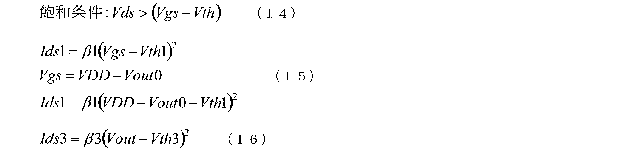
ここで、Ids1=Ids3であることから、負荷トランジスタ3611のゲインβ3は、以下の式(17)のように、求めることができる。
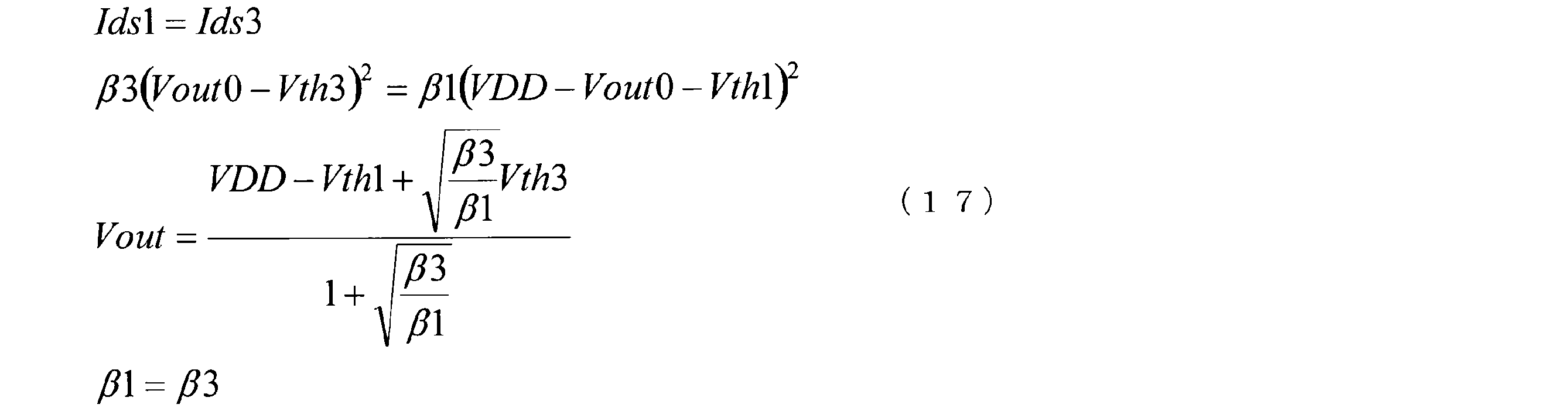
その結果、出力電圧Vout0は、以下の式(18)に表されるように、例えば、図20に示す例と比較して、略1/2に低減される。これは、出力電圧Vout0の変動範囲が略半分に制限されたことを示している。なお、出力電圧Vout0は、発振回路130に入力される。

(3.3.2.2.第2具体例)
図22は、本実施形態の第2具体例に係る調整回路の概略構成例を示す回路図である。なお、第2具体例では、出力電圧Voutの変動範囲をシフトさせるシフト回路362を用いて調整回路が構成されている場合について、例を挙げて説明する。
図22は、本実施形態の第2具体例に係る調整回路の概略構成例を示す回路図である。なお、第2具体例では、出力電圧Voutの変動範囲をシフトさせるシフト回路362を用いて調整回路が構成されている場合について、例を挙げて説明する。
図22に示すように、第2具体例に係るシフト回路362は、直列に接続されたP型の第1トランジスタ3621及びN型の第2トランジスタ3622と、同じく直列に接続されたP型の第3トランジスタ3623及びN型の第4トランジスタ3624とが、電源電圧VDDと接地電圧VSSとの間に並列に接続された構成を備える。言い換えれば、シフト回路362は、直列に接続されたP型トランジスタ及びN型トランジスタよりなる2つのCMOS(Complementary Metal-Oxide-Semiconductor)回路(以下、CMOSアナログ反転回路という)が直列接続された構成を備える。
第1トランジスタ3621と第2トランジスタ3622とは、ドレイン同士が接続されている。同様に、第3トランジスタ3623と第4トランジスタ3624とも、ドレイン同士が接続されている。
ソースフォロア回路からの出力電圧Voutは、第2トランジスタ3622のゲートに印加される。第1トランジスタ3621のゲートは、第1トランジスタ3621のドレイン及び第2トランジスタ3622のドレインに接続されるとともに、第3トランジスタ3623のゲートに接続されている。
第3トランジスタ3623のドレイン及び第4トランジスタ3624のドレインは、第4トランジスタ3624のゲートに接続されるとともに、後段の回路(例えば、制限回路361(又は発振回路130))に接続される。
以上のような構成を備えるシフト回路362では、直列接続されたP型のトランジスタ(第1トランジスタ3621又は第3トランジスタ3623)のオン抵抗とN型のトランジスタ(第2トランジスタ3622又は第4トランジスタ3624)のオン抵抗との比を制御することで、後段に出力される電圧の電圧値を制御することができる。
図23は、シフト回路におけるP型のトランジスタのオン抵抗とN型のトランジスタのオン抵抗との比を制御した場合の出力電圧のシフトを説明するための図である。図23において、破線L20は、P型のトランジスタ(第1トランジスタ3621又は第3トランジスタ3623)のオン抵抗とN型のトランジスタ(第2トランジスタ3622又は第4トランジスタ3624)のオン抵抗とを同じ抵抗値とした場合に後段に出力される電圧V1又はV2(シフト回路362からの出力電圧Vout1に相当)の電圧値を示している。
図22において、例えば、N型のトランジスタ(第2トランジスタ3622又は第4トランジスタ3624)のオン抵抗をP型のトランジスタ(第1トランジスタ3621又は第3トランジスタ3623)のオン抵抗よりも大きくした場合、図23の実線L21に示すように、後段に出力される電圧V1又はV2(出力電圧Vout1)は、高電圧側へシフトする。一方、P型のトランジスタ(第1トランジスタ3621又は第3トランジスタ3623)のオン抵抗をN型のトランジスタ(第2トランジスタ3622又は第4トランジスタ3624)のオン抵抗よりも大きくした場合、図23の実線L22に示すように、後段に出力される電圧V1又はV2(出力電圧Vout1)は、低電圧側へシフトする。
ただし、直列接続されたP型のトランジスタとN型のトランジスタとで構成されるCMOSアナログ反転回路を1段又は奇数段とした場合、図24の(a)から(b)に示すように、後段に出力される電圧(図22及び図24に示す例では例えば電圧V1)は、入力電圧Vinに対して反転した電圧値となる。そこで本実施形態では、P型のトランジスタとN型のトランジスタとで構成されるCMOSアナログ反転回路を2段又は偶数段とすることで、図24の(c)に示すように、出力される電圧を再反転させる(図22及び図24に示す例では例えば電圧V2)。
なお、図25に示すように、発振回路130の発振周波数fを上げたい場合には、出力電圧Vout1の電圧値を上げ、発振周波数fを下げたい場合には、出力電圧Vout1の電圧値を下げる必要がある。出力電圧Vout1の電圧値を上げる場合には、対角に位置する第2トランジスタ3622及び第3トランジスタ3623のオン抵抗を下げる。その際、反対側の対角に位置する第1トランジスタ3621及び第4トランジスタ3624のオン抵抗を上げてもよい。一方、出力電圧Vout1の電圧値を下げる場合には、第2トランジスタ3622及び第3トランジスタ3623のオン抵抗を上げる。その際、第1トランジスタ3621及び第4トランジスタ3624のオン抵抗を下げてもよい。
各トランジスタのオン抵抗の増減には、各トランジスタのゲート長(L長)やゲート幅(W長)を調節したり、各トランジスタのFinger数を調節したりする方法が採用されてもよい。
図26は、第1~第4トランジスタ3621~3624それぞれのFinger数を2とした場合のシフト回路362の概略構成例を示す回路図である。例えば、第1トランジスタ3621は、2つのトランジスタ3621a及び3621bから構成され、第2トランジスタ3622は、2つのトランジスタ3622a及び3622bから構成され、第3トランジスタ3623は、2つのトランジスタ3623a及び3623bから構成され、第4トランジスタ3624は、2つのトランジスタ3624a及び3624bから構成されている。
図27は、第1~第4トランジスタそれぞれのFinger数を切り替えた場合にシフト回路から出力される出力電圧の例を示すグラフである。図27において、破線±0は、第1~第4トランジスタ3621~3624それぞれのFinger数を1とした場合を示している。また、曲線P1は、第2トランジスタ3622及び第3トランジスタ3623の合計のFinger数を3とし、第1トランジスタ3621及び第4トランジスタ3624の合計のFinger数を2とした場合を示し、曲線P2は、第2トランジスタ3622及び第3トランジスタ3623の合計のFinger数を3とし、第1トランジスタ3621及び第4トランジスタ3624の合計のFinger数を1とした場合を示し、曲線P3は、第2トランジスタ3622及び第3トランジスタ3623の合計のFinger数を4とし、第1トランジスタ3621及び第4トランジスタ3624の合計のFinger数を2とした場合を示し、曲線P4は、第2トランジスタ3622及び第3トランジスタ3623の合計のFinger数を4とし、第1トランジスタ3621及び第4トランジスタ3624の合計のFinger数を1とした場合を示している。さらに、曲線M1は、第2トランジスタ3622及び第3トランジスタ3623の合計のFinger数を2とし、第1トランジスタ3621及び第4トランジスタ3624の合計のFinger数を3とした場合を示し、曲線M2は、第2トランジスタ3622及び第3トランジスタ3623の合計のFinger数を1とし、第1トランジスタ3621及び第4トランジスタ3624の合計のFinger数を3とした場合を示し、曲線M3は、第2トランジスタ3622及び第3トランジスタ3623の合計のFinger数を2とし、第1トランジスタ3621及び第4トランジスタ3624の合計のFinger数を4とした場合を示し、曲線M4は、第2トランジスタ3622及び第3トランジスタ3623の合計のFinger数を1とし、第1トランジスタ3621及び第4トランジスタ3624の合計のFinger数を4とした場合を示している。
このように、合計8個のトランジスタをカスコード接続した構成では、各トランジスタのFinger数を調整することで、出力電圧Vout1の電圧値を9段階に調整することが可能である。
(3.3.2.3.第3具体例)
図28は、本実施形態の第3具体例に係る調整回路の概略構成例を示す回路図である。図28に示すように、第3具体例に係る調整回路360は、測定トランジスタ111及び参照トランジスタ110が構成するソースフォロア回路に対して、制限回路361とシフト回路362とが直列に接続された構成を有していてもよい。また、シフト回路362は、抵抗素子3625で構成されていてもよい。
図28は、本実施形態の第3具体例に係る調整回路の概略構成例を示す回路図である。図28に示すように、第3具体例に係る調整回路360は、測定トランジスタ111及び参照トランジスタ110が構成するソースフォロア回路に対して、制限回路361とシフト回路362とが直列に接続された構成を有していてもよい。また、シフト回路362は、抵抗素子3625で構成されていてもよい。
抵抗素子3625をソースフォロア回路のソース側に設けることで、出力電圧Vout0を高電圧側へシフトさせることができる。なお、出力電圧をVout0を低電圧側へシフトさせる場合は、抵抗素子3625をソースフォロア回路のドレイン側へ設ければよい。
(3.3.2.4.第4具体例)
図29は、本実施形態の第4具体例に係る調整回路の概略構成例を示す回路図である。図29に示すように、第4具体例に係る調整回路360は、第3具体例に係る調整回路360と同様の構成において、シフト回路362が、2つのトランジスタ3626及び3627と、定電流回路3628とを備える回路構成に置き換えられた構成を備える。
図29は、本実施形態の第4具体例に係る調整回路の概略構成例を示す回路図である。図29に示すように、第4具体例に係る調整回路360は、第3具体例に係る調整回路360と同様の構成において、シフト回路362が、2つのトランジスタ3626及び3627と、定電流回路3628とを備える回路構成に置き換えられた構成を備える。
2つのトランジスタ3626及び3627は、互いのゲートが一方のトランジスタ3627のドレインに接続されることで、カレントミラー回路を構成している。トランジスタ3627のドレインは、定電流回路3628に接続されている。
このような構成では、カレントミラー回路を構成する一方のトランジスタ3626がソースフォロア回路に流れる電流を制限するように機能する。したがって、定電流回路3628に流れる電流を制御することで、出力電圧Vout0を高電圧側へシフトさせることが可能となる。なお、出力電圧Vout0を低電圧側へシフトさせる場合には、シフト回路362をソースフォロア回路のドレイン側に設ければよい。
(3.3.2.5.その他の例)
また、例えば、図21を用いて説明した構成において、測定トランジスタ111又は参照トランジスタ110と、負荷トランジスタ3611とのオン抵抗の比を調整することでも、出力電圧Vout0をシフトさせることが可能である。なお、各トランジスタのオン抵抗の増減には、各トランジスタのゲート長(L長)やゲート幅(W長)を調節したり、各トランジスタのFinger数を調節したりする方法が採用されてもよい。
また、例えば、図21を用いて説明した構成において、測定トランジスタ111又は参照トランジスタ110と、負荷トランジスタ3611とのオン抵抗の比を調整することでも、出力電圧Vout0をシフトさせることが可能である。なお、各トランジスタのオン抵抗の増減には、各トランジスタのゲート長(L長)やゲート幅(W長)を調節したり、各トランジスタのFinger数を調節したりする方法が採用されてもよい。
(3.4.構造例)
つぎに、図面を参照して、本の実施形態に係る半導体装置の構造例について、幾つか例を挙げて説明する。なお、以下の説明において、制限回路361及びシフト回路362は、上述した調整回路360の説明において例示した制限回路361及びシフト回路362と同様であってよい。
つぎに、図面を参照して、本の実施形態に係る半導体装置の構造例について、幾つか例を挙げて説明する。なお、以下の説明において、制限回路361及びシフト回路362は、上述した調整回路360の説明において例示した制限回路361及びシフト回路362と同様であってよい。
(3.4.1.第1例)
図30は、本実施形態の第1例に係る半導体装置の構造例を説明する回路図である。図30に示すように、第1例に係る半導体装置30-1は、例えば、第1の実施形態において図3を用いて説明した半導体装置10と同様の構成において、測定トランジスタ111及び参照トランジスタ110が構成するソースフォロア回路のソース側に、制限回路361よりなる調整回路360が設けられた構造を備える。
図30は、本実施形態の第1例に係る半導体装置の構造例を説明する回路図である。図30に示すように、第1例に係る半導体装置30-1は、例えば、第1の実施形態において図3を用いて説明した半導体装置10と同様の構成において、測定トランジスタ111及び参照トランジスタ110が構成するソースフォロア回路のソース側に、制限回路361よりなる調整回路360が設けられた構造を備える。
(3.4.2.第2例)
図31は、本実施形態の第2例に係る半導体装置の構造例を説明する回路図である。図31に示すように、第2例に係る半導体装置30-2は、例えば、図30に示す半導体装置30-1と同様の構成において、制限回路361よりなる調整回路360が発振回路130と接地電圧VSSとの間に設けられた構造を備える。
図31は、本実施形態の第2例に係る半導体装置の構造例を説明する回路図である。図31に示すように、第2例に係る半導体装置30-2は、例えば、図30に示す半導体装置30-1と同様の構成において、制限回路361よりなる調整回路360が発振回路130と接地電圧VSSとの間に設けられた構造を備える。
(3.4.3.第3例)
図32は、本実施形態の第3例に係る半導体装置の構造例を説明する回路図である。図32に示すように、第3例に係る半導体装置30-3は、例えば、図30に示す半導体装置30-1と同様の構成において、制限回路361よりなる調整回路360がソースフォロア回路のドレイン側に設けられた構造を備える。
図32は、本実施形態の第3例に係る半導体装置の構造例を説明する回路図である。図32に示すように、第3例に係る半導体装置30-3は、例えば、図30に示す半導体装置30-1と同様の構成において、制限回路361よりなる調整回路360がソースフォロア回路のドレイン側に設けられた構造を備える。
(3.4.4.第4例)
図33は、本実施形態の第4例に係る半導体装置の構造例を説明する回路図である。図33に示すように、第4例に係る半導体装置30-4は、例えば、図32に示す半導体装置30-3と同様の構成において、発振回路130が調整回路360と電源電圧VDDとの間に設けられた構造を備える。
図33は、本実施形態の第4例に係る半導体装置の構造例を説明する回路図である。図33に示すように、第4例に係る半導体装置30-4は、例えば、図32に示す半導体装置30-3と同様の構成において、発振回路130が調整回路360と電源電圧VDDとの間に設けられた構造を備える。
(3.4.5.第5例)
図34は、本実施形態の第5例に係る半導体装置の構造例を説明する回路図である。図34に示すように、第5例に係る半導体装置30-5は、例えば、第1の実施形態において図3を用いて説明した半導体装置10と同様の構成において、測定トランジスタ111及び参照トランジスタ110が構成するソースフォロア回路のソース側にシフト回路362が接続され、シフト回路362の出力に制限回路361が接続された構造を備える。
図34は、本実施形態の第5例に係る半導体装置の構造例を説明する回路図である。図34に示すように、第5例に係る半導体装置30-5は、例えば、第1の実施形態において図3を用いて説明した半導体装置10と同様の構成において、測定トランジスタ111及び参照トランジスタ110が構成するソースフォロア回路のソース側にシフト回路362が接続され、シフト回路362の出力に制限回路361が接続された構造を備える。
(3.4.6.第6例)
図35は、本実施形態の第6例に係る半導体装置の構造例を説明する回路図である。図35に示すように、第6例に係る半導体装置30-6は、例えば、図34に示す半導体装置30-5と同様の構成において、制限回路361がソースフォロア回路のドレイン側に接続され、シフト回路362の出力に発振回路130が接続された構造を備える。
図35は、本実施形態の第6例に係る半導体装置の構造例を説明する回路図である。図35に示すように、第6例に係る半導体装置30-6は、例えば、図34に示す半導体装置30-5と同様の構成において、制限回路361がソースフォロア回路のドレイン側に接続され、シフト回路362の出力に発振回路130が接続された構造を備える。
(3.4.7.その他の例)
なお、上述した第1例から第6例では、ソースフォロア回路を構成する測定トランジスタ111及び参照トランジスタ110がN型のトランジスタである場合を例示したが、これに限定されるものではない。すなわち、本実施形態では、測定トランジスタ111及び参照トランジスタ110をP型のトランジスタで構成することも可能である。その場合、例えば、第1例から第6例において説明した構造において、電源電圧VDDと接地電圧VSSとが入れ替えられることとなる。
なお、上述した第1例から第6例では、ソースフォロア回路を構成する測定トランジスタ111及び参照トランジスタ110がN型のトランジスタである場合を例示したが、これに限定されるものではない。すなわち、本実施形態では、測定トランジスタ111及び参照トランジスタ110をP型のトランジスタで構成することも可能である。その場合、例えば、第1例から第6例において説明した構造において、電源電圧VDDと接地電圧VSSとが入れ替えられることとなる。
(3.5.実証実験結果)
つづいて、以上で説明した調整回路360を設けることによる効果について、実証実験結果に基づいて説明する。図36は、本実証実験を実行するにあたり使用した半導体装置の回路構成を示す図である。また、図37は、本実証実験により得られた結果を示すグラフである。
つづいて、以上で説明した調整回路360を設けることによる効果について、実証実験結果に基づいて説明する。図36は、本実証実験を実行するにあたり使用した半導体装置の回路構成を示す図である。また、図37は、本実証実験により得られた結果を示すグラフである。
図36に示すように、本実証実験では、測定トランジスタ111及び参照トランジスタ110が構成するソースフォロア回路のソース側に調整回路360が設けられた半導体装置を使用した。調整回路360には、図21を用いて説明した第1具体例に係る制限回路361を使用した。
この半導体装置において、ソースフォロア回路から出力された出力電圧Voutは、発振回路130に入力される。発振回路130の発振周波数は、出力パッド391を介して計測した。発振回路130には、リングオシレータを使用した。
また、本実証実験では、ソースフォロア回路からの出力電圧Voutを直接計測するために、ソースフォロア回路の出力を分岐してスイッチ380を介して出力パッド392に接続した。
本検証実験では、以上のような構成において、発振回路130に入力するイネーブル信号ENをオフにした状態でスイッチ380をオンにすることで、測定トランジスタ111に電圧Vg1を印加した際のソースフォロア回路からの出力電圧Vout(これを出力電圧Vout1とする)と、参照トランジスタ110に電圧Vg2を印加した際のソースフォロア回路からの出力電圧Vout(これを出力電圧Vout2とする)とを、出力パッド392を介して直接計測した。また、本実験では、スイッチ380をオフにした状態イネーブル信号ENをオンにすることで、測定トランジスタ111に電圧Vg1を印加した際の発振回路130の発振周波数F1と、参照トランジスタ110に電圧Vg2を印加した際の発振回路130の発振周波数F2とも、出力パッド391を介して計測した。
図37において、破線は、発振周波数F2から発振周波数F1を引き算して所定の比例乗数を乗算した値をプロットしたものであり、実線は、出力電圧Vout2から出力電圧Vout1を引き算した値をプロットしたものである。図37を参照すると分かるように、発振周波数F2から発振周波数F1を引き算して所定の比例乗数を乗算した値と、出力電圧Vout2から出力電圧Vout1を引き算した値とは、略一致している。これは、周波数差に所定の比例乗数を乗算することで、出力電圧Voutの変動を取得することができることを示している。
(3.5.1.制限回路を構成する負荷トランジスタの閾値電圧による影響について)
ここで、制限回路361を構成する負荷トランジスタ3611の閾値電圧Vthがソースフォロア回路からの出力電圧Voutに与える影響について説明する。
ここで、制限回路361を構成する負荷トランジスタ3611の閾値電圧Vthがソースフォロア回路からの出力電圧Voutに与える影響について説明する。
参照トランジスタ110に電圧Vg2を印加した際の出力電圧Vout2は以下の式(19)で求めることができ、測定トランジスタ111に電圧Vg1を印加した際の出力電圧Vout1は以下の式(20)で求めることができる。

ここで、各トランジスタの閾値電圧の設計値をVthとし、測定トランジスタ111の閾値電圧Vth1のバラツキをδVth1とし、参照トランジスタ110の閾値電圧Vth2のバラツキをδVth2とし、アンテナからのダメージによる閾値電圧Vth1のシフト量をΔPIDとすると、参照トランジスタ110の閾値電圧Vth2は以下の式(21)で表され、測定トランジスタ111の閾値電圧Vth1は以下の式(22)で表される。

したがって、以下の式(23)のように、出力電圧Vout2から出力電圧Vout1を引き算した場合、参照トランジスタ110の閾値電圧Vth2のバラツキδVth2と測定トランジスタ111の閾値電圧Vth1のバラツキδVth1との差(-δVth2+δVth1)(以下、ミスマッチ成分ともいう)と、アンテナからのダメージによる閾値電圧Vth1のシフト量ΔPIDとの成分が残留することが分かる。

出力電圧Voutは、発振回路130に入力されて発振周波数fに変換される。出力電圧Vout2での発振周波数fはF2であり、出力電圧Vout1での発振周波数fはF1である。また、発振周波数fは、以下の式(24)及び式(25)に示すように、関数G(f)により電圧値に変化可能である。

本実施形態では、上述したように、線形近似が可能であることから、kを係数(比例乗数)とした場合、閾値電圧Vth1及びVth2は、以下の式(26)のように近似することができる。

したがって、参照トランジスタ110の閾値電圧Vth2と測定トランジスタ111の閾値電圧Vth1との差、すなわち、アンテナからのダメージによる閾値電圧Vth1のシフト量ΔPIDは、以下の式(27)のように求めることが可能である。

なお、式(27)には、ミスマッチ成分(δVth1-δVth2)が残留しているが、このミスマッチ成分は完全なランダム値であるため、十分な数のサンプルを測定し、その平均を取ることで、無視できる程度に低減させることが可能である。
図38は、アンテナからのダメージを受けた場合と受けていない場合とのミスマッチ成分の電圧値の例を示すグラフである。図38において、黒く塗りつぶされた丸は、アンテナからのダメージを受けていない場合の閾値電圧Vthを示し、白抜きの丸は、アンテナからのダメージを受けた場合の閾値電圧を示している。
図38に示すように、アンテナからのダメージを受けていない場合では、閾値電圧Vthの平均値は-0.0004[V]であったのに対し、アンテナからのダメージを受けた場合では、閾値電圧Vthの平均値は0.039[V]であった。これは、測定トランジスタ111の閾値電圧Vthがアンテナからのダメージにより平均して0.039Vシフトしたことを示している。
(3.6.まとめ)
以上のように、本実施形態によれば、線形近似を利用した簡便な方法により、PIDによるチャネル抵抗R1又は閾値電圧Vthの変動量を算出することが可能な半導体装置、検出方法、電子機器及び電子機器の制御方法が実現される。
以上のように、本実施形態によれば、線形近似を利用した簡便な方法により、PIDによるチャネル抵抗R1又は閾値電圧Vthの変動量を算出することが可能な半導体装置、検出方法、電子機器及び電子機器の制御方法が実現される。
その他の構成、動作及び効果については、上述した実施形態と同様であってよいため、ここでは詳細な説明を省略する。
以上、添付図面を参照しながら本開示の好適な実施形態について詳細に説明したが、本開示の技術的範囲はかかる例に限定されない。本開示の技術分野における通常の知識を有する者であれば、請求の範囲に記載された技術的思想の範疇内において、各種の変更例または修正例に想到し得ることは明らかであり、これらについても、当然に本開示の技術的範囲に属するものと了解される。
また、本明細書に記載された効果は、あくまで説明的または例示的なものであって限定的ではない。つまり、本開示に係る技術は、上記の効果とともに、または上記の効果に代えて、本明細書の記載から当業者には明らかな他の効果を奏しうる。
なお、以下のような構成も本開示の技術的範囲に属する。
(1)
プラズマプロセスにてアンテナとして機能するアンテナ部がゲートに電気的に接続された少なくとも1以上の測定トランジスタと、
前記測定トランジスタの前記ゲートにソースが前記アンテナ部と並列に電気的に接続された選択トランジスタと、
前記測定トランジスタのソースと電気的に接続され、発振周波数が前記測定トランジスタの閾値電圧によって変動する発振回路と、
を備える、半導体装置。
(2)
前記発振回路は、VDD配線及びVSS配線の間に設けられ、
前記測定トランジスタは、前記発振回路と、前記VDD配線又は前記VSS配線との間に設けられる、前記(1)に記載の半導体装置。
(3)
前記発振回路は、リングオシレータである、前記(2)に記載の半導体装置。
(4)
前記発振回路は、出力される発振周波数が入力電圧によって変動する発振回路であり、
前記発振回路の入力は、前記測定トランジスタのソースに負荷素子と並列に電気的に接続される、前記(1)に記載の半導体装置。
(5)
前記負荷素子は、抵抗素子である、前記(4)に記載の半導体装置。
(6)
前記測定トランジスタ及び前記選択トランジスタは、同じ導電型のトランジスタである、前記(1)~(5)のいずれか一項に記載の半導体装置。
(7)
前記測定トランジスタは、複数設けられ、
前記発振回路よりもVDD配線側に設けられた前記測定トランジスタは、N型トランジスタであり、前記発振回路よりもVSS配線側に設けられた前記測定トランジスタは、P型トランジスタである、前記(1)~(6)のいずれか一項に記載の半導体装置。
(8)
前記測定トランジスタは、複数設けられ、
複数の前記測定トランジスタの各々では、前記アンテナ部と前記ゲートとの面積比が互いに異なる、前記(1)~(7)のいずれか一項に記載の半導体装置。
(9)
前記測定トランジスタの前記ゲートには、さらに保護素子が電気的に接続される、前記(1)~(8)のいずれか一項に記載の半導体装置。
(10)
前記選択トランジスタは、前記アンテナ部よりも上層の配線で前記測定トランジスタと電気的に接続され、
前記配線には、保護素子が電気的に接続される、前記(1)~(9)のいずれか一項に記載の半導体装置。
(11)
前記測定トランジスタのボディは、前記測定トランジスタのソースと電気的に接続される、前記(1)~(10)のいずれか一項に記載の半導体装置。
(12)
前記アンテナ部とゲートが電気的に接続されず、前記発振回路とソースが電気的に接続される参照トランジスタと、
前記参照トランジスタの前記ゲートにソースが電気的に接続された参照用選択トランジスタと、
をさらに備える、前記(1)~(11)のいずれか一項に記載の半導体装置。
(13)
前記測定トランジスタの前記ソースに出現する電圧の電圧値を調整する調整回路をさらに備える、前記(1)~(12)の何れか一項に記載の半導体装置。
(14)
前記調整回路は、前記測定トランジスタの前記ソース及びドレインのうち少なくとも一方に接続されている、前記(13)に記載の半導体装置。
(15)
前記調整回路は、抵抗素子を含む、前記(13)又は(14)に記載の半導体装置。
(16)
前記調整回路は、CMOS(Complementary Metal-Oxide-Semiconductor)素子を含む、前記(13)又は(14)に記載の半導体装置。
(17)
前記発振回路は、出力される発振周波数が入力電圧の電圧値によって変動する発振回路であり、
前記発振回路の入力は、前記測定トランジスタの前記ソースに負荷素子と並列に電気的に接続される、
前記(13)~(16)の何れか一項に記載の半導体装置。
(18)
プラズマプロセスにてアンテナとして機能するアンテナ部がゲートに電気的に接続された少なくとも1以上の測定トランジスタと、前記測定トランジスタの前記ゲートにソースが前記アンテナ部と並列に電気的に接続された選択トランジスタと、前記測定トランジスタのソースと電気的に接続され、発振周波数が前記測定トランジスタの閾値電圧によって変動する発振回路と、を備える半導体装置の前記選択トランジスタをオン状態に制御することで、前記測定トランジスタをオン状態に制御することと、
前記測定トランジスタがオン状態の時に前記発振回路の発振周波数を測定することと、 測定された前記発振周波数に基づいて、前記測定トランジスタの閾値電圧と、前記閾値電圧の理想値との差分の有無を検出することと、
を含む、検出方法。
(19)
プラズマプロセスにてアンテナとして機能するアンテナ部がゲートに電気的に接続された少なくとも1以上の測定トランジスタと、前記測定トランジスタの前記ゲートにソースが前記アンテナ部と並列に電気的に接続された選択トランジスタと、前記測定トランジスタのソースと電気的に接続され、発振周波数が前記測定トランジスタの閾値電圧によって変動する発振回路と、を有する半導体装置と、
前記選択トランジスタのオン又はオフ状態を制御することで、前記測定トランジスタのオン又はオフ状態を制御する制御部と、
前記測定トランジスタがオン状態の時に前記発振回路の発振周波数を測定する測定部と、
測定された前記発振周波数の各々に基づいて、前記測定トランジスタの閾値電圧と、前記閾値電圧の理想値との差分の有無を検出する検出部と、
前記検出部にて前記差分が検出された場合、前記プラズマプロセスによる影響を補正する処理を行う処理部と、
を備える、電子機器。
(20)
プラズマプロセスにてアンテナとして機能するアンテナ部がゲートに電気的に接続された少なくとも1以上の測定トランジスタと、前記測定トランジスタの前記ゲートにソースが前記アンテナ部と並列に電気的に接続された選択トランジスタと、前記測定トランジスタのソースと電気的に接続され、発振周波数が前記測定トランジスタの閾値電圧によって変動する発振回路と、を有する半導体装置を備える電子機器の前記選択トランジスタをオン状態に制御することで、前記測定トランジスタをオン状態に制御することと、
前記測定トランジスタがオン状態の時に前記発振回路の発振周波数を測定することと、 測定された前記発振周波数に基づいて、前記測定トランジスタの閾値電圧と、前記閾値電圧の理想値との差分の有無を検出することと、
前記差分が検出された場合、前記プラズマプロセスによる影響を補正する制御を行うことと、
を含む、電子機器の制御方法。
(1)
プラズマプロセスにてアンテナとして機能するアンテナ部がゲートに電気的に接続された少なくとも1以上の測定トランジスタと、
前記測定トランジスタの前記ゲートにソースが前記アンテナ部と並列に電気的に接続された選択トランジスタと、
前記測定トランジスタのソースと電気的に接続され、発振周波数が前記測定トランジスタの閾値電圧によって変動する発振回路と、
を備える、半導体装置。
(2)
前記発振回路は、VDD配線及びVSS配線の間に設けられ、
前記測定トランジスタは、前記発振回路と、前記VDD配線又は前記VSS配線との間に設けられる、前記(1)に記載の半導体装置。
(3)
前記発振回路は、リングオシレータである、前記(2)に記載の半導体装置。
(4)
前記発振回路は、出力される発振周波数が入力電圧によって変動する発振回路であり、
前記発振回路の入力は、前記測定トランジスタのソースに負荷素子と並列に電気的に接続される、前記(1)に記載の半導体装置。
(5)
前記負荷素子は、抵抗素子である、前記(4)に記載の半導体装置。
(6)
前記測定トランジスタ及び前記選択トランジスタは、同じ導電型のトランジスタである、前記(1)~(5)のいずれか一項に記載の半導体装置。
(7)
前記測定トランジスタは、複数設けられ、
前記発振回路よりもVDD配線側に設けられた前記測定トランジスタは、N型トランジスタであり、前記発振回路よりもVSS配線側に設けられた前記測定トランジスタは、P型トランジスタである、前記(1)~(6)のいずれか一項に記載の半導体装置。
(8)
前記測定トランジスタは、複数設けられ、
複数の前記測定トランジスタの各々では、前記アンテナ部と前記ゲートとの面積比が互いに異なる、前記(1)~(7)のいずれか一項に記載の半導体装置。
(9)
前記測定トランジスタの前記ゲートには、さらに保護素子が電気的に接続される、前記(1)~(8)のいずれか一項に記載の半導体装置。
(10)
前記選択トランジスタは、前記アンテナ部よりも上層の配線で前記測定トランジスタと電気的に接続され、
前記配線には、保護素子が電気的に接続される、前記(1)~(9)のいずれか一項に記載の半導体装置。
(11)
前記測定トランジスタのボディは、前記測定トランジスタのソースと電気的に接続される、前記(1)~(10)のいずれか一項に記載の半導体装置。
(12)
前記アンテナ部とゲートが電気的に接続されず、前記発振回路とソースが電気的に接続される参照トランジスタと、
前記参照トランジスタの前記ゲートにソースが電気的に接続された参照用選択トランジスタと、
をさらに備える、前記(1)~(11)のいずれか一項に記載の半導体装置。
(13)
前記測定トランジスタの前記ソースに出現する電圧の電圧値を調整する調整回路をさらに備える、前記(1)~(12)の何れか一項に記載の半導体装置。
(14)
前記調整回路は、前記測定トランジスタの前記ソース及びドレインのうち少なくとも一方に接続されている、前記(13)に記載の半導体装置。
(15)
前記調整回路は、抵抗素子を含む、前記(13)又は(14)に記載の半導体装置。
(16)
前記調整回路は、CMOS(Complementary Metal-Oxide-Semiconductor)素子を含む、前記(13)又は(14)に記載の半導体装置。
(17)
前記発振回路は、出力される発振周波数が入力電圧の電圧値によって変動する発振回路であり、
前記発振回路の入力は、前記測定トランジスタの前記ソースに負荷素子と並列に電気的に接続される、
前記(13)~(16)の何れか一項に記載の半導体装置。
(18)
プラズマプロセスにてアンテナとして機能するアンテナ部がゲートに電気的に接続された少なくとも1以上の測定トランジスタと、前記測定トランジスタの前記ゲートにソースが前記アンテナ部と並列に電気的に接続された選択トランジスタと、前記測定トランジスタのソースと電気的に接続され、発振周波数が前記測定トランジスタの閾値電圧によって変動する発振回路と、を備える半導体装置の前記選択トランジスタをオン状態に制御することで、前記測定トランジスタをオン状態に制御することと、
前記測定トランジスタがオン状態の時に前記発振回路の発振周波数を測定することと、 測定された前記発振周波数に基づいて、前記測定トランジスタの閾値電圧と、前記閾値電圧の理想値との差分の有無を検出することと、
を含む、検出方法。
(19)
プラズマプロセスにてアンテナとして機能するアンテナ部がゲートに電気的に接続された少なくとも1以上の測定トランジスタと、前記測定トランジスタの前記ゲートにソースが前記アンテナ部と並列に電気的に接続された選択トランジスタと、前記測定トランジスタのソースと電気的に接続され、発振周波数が前記測定トランジスタの閾値電圧によって変動する発振回路と、を有する半導体装置と、
前記選択トランジスタのオン又はオフ状態を制御することで、前記測定トランジスタのオン又はオフ状態を制御する制御部と、
前記測定トランジスタがオン状態の時に前記発振回路の発振周波数を測定する測定部と、
測定された前記発振周波数の各々に基づいて、前記測定トランジスタの閾値電圧と、前記閾値電圧の理想値との差分の有無を検出する検出部と、
前記検出部にて前記差分が検出された場合、前記プラズマプロセスによる影響を補正する処理を行う処理部と、
を備える、電子機器。
(20)
プラズマプロセスにてアンテナとして機能するアンテナ部がゲートに電気的に接続された少なくとも1以上の測定トランジスタと、前記測定トランジスタの前記ゲートにソースが前記アンテナ部と並列に電気的に接続された選択トランジスタと、前記測定トランジスタのソースと電気的に接続され、発振周波数が前記測定トランジスタの閾値電圧によって変動する発振回路と、を有する半導体装置を備える電子機器の前記選択トランジスタをオン状態に制御することで、前記測定トランジスタをオン状態に制御することと、
前記測定トランジスタがオン状態の時に前記発振回路の発振周波数を測定することと、 測定された前記発振周波数に基づいて、前記測定トランジスタの閾値電圧と、前記閾値電圧の理想値との差分の有無を検出することと、
前記差分が検出された場合、前記プラズマプロセスによる影響を補正する制御を行うことと、
を含む、電子機器の制御方法。
10、10A、11、12、13、14、20、30-1~30-6 半導体装置
101 制御部
102 測定部
103 検出部
104 処理部
110、210 参照トランジスタ
111、111A、112、211、212 測定トランジスタ
120、220 参照用選択トランジスタ
121、122、221、222 選択トランジスタ
130、230 発振回路
131 P型トランジスタ
132 N型トランジスタ
133 負荷容量
140、141、142、241、242 アンテナ部
150 保護素子
250 負荷素子
360 調整回路
361 制限回路
362 シフト回路
380 スイッチ
391、392 出力パッド
1000、1001、1002 電子機器
1101、1102 本体回路
1201 基準電圧制御回路
1202 PID耐性ブロック切替制御回路
1301 基準電圧生成回路
1302 PID低耐性回路
1402 PID高耐性回路
3611 負荷トランジスタ
3621 第1トランジスタ
3621a、3621b、3622a、3622b、3623a、3623b、3624a、3624b、3626、3627 トランジスタ
3622 第2トランジスタ
3623 第3トランジスタ
3624 第4トランジスタ
3625 抵抗素子
3628 定電流回路
101 制御部
102 測定部
103 検出部
104 処理部
110、210 参照トランジスタ
111、111A、112、211、212 測定トランジスタ
120、220 参照用選択トランジスタ
121、122、221、222 選択トランジスタ
130、230 発振回路
131 P型トランジスタ
132 N型トランジスタ
133 負荷容量
140、141、142、241、242 アンテナ部
150 保護素子
250 負荷素子
360 調整回路
361 制限回路
362 シフト回路
380 スイッチ
391、392 出力パッド
1000、1001、1002 電子機器
1101、1102 本体回路
1201 基準電圧制御回路
1202 PID耐性ブロック切替制御回路
1301 基準電圧生成回路
1302 PID低耐性回路
1402 PID高耐性回路
3611 負荷トランジスタ
3621 第1トランジスタ
3621a、3621b、3622a、3622b、3623a、3623b、3624a、3624b、3626、3627 トランジスタ
3622 第2トランジスタ
3623 第3トランジスタ
3624 第4トランジスタ
3625 抵抗素子
3628 定電流回路
Claims (20)
- プラズマプロセスにてアンテナとして機能するアンテナ部がゲートに電気的に接続された少なくとも1以上の測定トランジスタと、
前記測定トランジスタの前記ゲートにソースが前記アンテナ部と並列に電気的に接続された選択トランジスタと、
前記測定トランジスタのソースと電気的に接続され、発振周波数が前記測定トランジスタの閾値電圧によって変動する発振回路と、
を備える、半導体装置。 - 前記発振回路は、VDD配線及びVSS配線の間に設けられ、
前記測定トランジスタは、前記発振回路と、前記VDD配線又は前記VSS配線との間に設けられる、請求項1に記載の半導体装置。 - 前記発振回路は、リングオシレータである、請求項2に記載の半導体装置。
- 前記発振回路は、出力される発振周波数が入力電圧によって変動する発振回路であり、
前記発振回路の入力は、前記測定トランジスタのソースに負荷素子と並列に電気的に接続される、請求項1に記載の半導体装置。 - 前記負荷素子は、抵抗素子である、請求項4に記載の半導体装置。
- 前記測定トランジスタ及び前記選択トランジスタは、同じ導電型のトランジスタである、請求項1に記載の半導体装置。
- 前記測定トランジスタは、複数設けられ、
前記発振回路よりもVDD配線側に設けられた前記測定トランジスタは、N型トランジスタであり、前記発振回路よりもVSS配線側に設けられた前記測定トランジスタは、P型トランジスタである、請求項1に記載の半導体装置。 - 前記測定トランジスタは、複数設けられ、
複数の前記測定トランジスタの各々では、前記アンテナ部と前記ゲートとの面積比が互いに異なる、請求項1に記載の半導体装置。 - 前記測定トランジスタの前記ゲートには、さらに保護素子が電気的に接続される、請求項1に記載の半導体装置。
- 前記選択トランジスタは、前記アンテナ部よりも上層の配線で前記測定トランジスタと電気的に接続され、
前記配線には、保護素子が電気的に接続される、請求項1に記載の半導体装置。 - 前記測定トランジスタのボディは、前記測定トランジスタのソースと電気的に接続される、請求項1に記載の半導体装置。
- 前記アンテナ部とゲートが電気的に接続されず、前記発振回路とソースが電気的に接続される参照トランジスタと、
前記参照トランジスタの前記ゲートにソースが電気的に接続された参照用選択トランジスタと、
をさらに備える、請求項1に記載の半導体装置。 - 前記測定トランジスタの前記ソースに出現する電圧の電圧値を調整する調整回路をさらに備える、請求項1に記載の半導体装置。
- 前記調整回路は、前記測定トランジスタの前記ソース及びドレインのうち少なくとも一方に接続されている、請求項13に記載の半導体装置。
- 前記調整回路は、抵抗素子を含む、請求項13に記載の半導体装置。
- 前記調整回路は、CMOS(Complementary Metal-Oxide-Semiconductor)素子を含む、請求項13に記載の半導体装置。
- 前記発振回路は、出力される発振周波数が入力電圧の電圧値によって変動する発振回路であり、
前記発振回路の入力は、前記測定トランジスタの前記ソースに負荷素子と並列に電気的に接続される、
請求項13に記載の半導体装置。 - プラズマプロセスにてアンテナとして機能するアンテナ部がゲートに電気的に接続された少なくとも1以上の測定トランジスタと、前記測定トランジスタの前記ゲートにソースが前記アンテナ部と並列に電気的に接続された選択トランジスタと、前記測定トランジスタのソースと電気的に接続され、発振周波数が前記測定トランジスタの閾値電圧によって変動する発振回路と、を備える半導体装置の前記選択トランジスタをオン状態に制御することで、前記測定トランジスタをオン状態に制御することと、
前記測定トランジスタがオン状態の時に前記発振回路の発振周波数を測定することと、 測定された前記発振周波数に基づいて、前記測定トランジスタの閾値電圧と、前記閾値電圧の理想値との差分の有無を検出することと、
を含む、検出方法。 - プラズマプロセスにてアンテナとして機能するアンテナ部がゲートに電気的に接続された少なくとも1以上の測定トランジスタと、前記測定トランジスタの前記ゲートにソースが前記アンテナ部と並列に電気的に接続された選択トランジスタと、前記測定トランジスタのソースと電気的に接続され、発振周波数が前記測定トランジスタの閾値電圧によって変動する発振回路と、を有する半導体装置と、
前記選択トランジスタのオン又はオフ状態を制御することで、前記測定トランジスタのオン又はオフ状態を制御する制御部と、
前記測定トランジスタがオン状態の時に前記発振回路の発振周波数を測定する測定部と、
測定された前記発振周波数の各々に基づいて、前記測定トランジスタの閾値電圧と、前記閾値電圧の理想値との差分の有無を検出する検出部と、
前記検出部にて前記差分が検出された場合、前記プラズマプロセスによる影響を補正する処理を行う処理部と、
を備える、電子機器。 - プラズマプロセスにてアンテナとして機能するアンテナ部がゲートに電気的に接続された少なくとも1以上の測定トランジスタと、前記測定トランジスタの前記ゲートにソースが前記アンテナ部と並列に電気的に接続された選択トランジスタと、前記測定トランジスタのソースと電気的に接続され、発振周波数が前記測定トランジスタの閾値電圧によって変動する発振回路と、を有する半導体装置を備える電子機器の前記選択トランジスタをオン状態に制御することで、前記測定トランジスタをオン状態に制御することと、
前記測定トランジスタがオン状態の時に前記発振回路の発振周波数を測定することと、 測定された前記発振周波数に基づいて、前記測定トランジスタの閾値電圧と、前記閾値電圧の理想値との差分の有無を検出することと、
前記差分が検出された場合、前記プラズマプロセスによる影響を補正する制御を行うことと、
を含む、電子機器の制御方法。
Priority Applications (1)
| Application Number | Priority Date | Filing Date | Title |
|---|---|---|---|
| US17/283,153 US20210389362A1 (en) | 2018-10-17 | 2019-10-16 | Semiconductor device, detection method, electronic apparatus, and electronic apparatus control method |
Applications Claiming Priority (2)
| Application Number | Priority Date | Filing Date | Title |
|---|---|---|---|
| JP2018195635A JP2020064965A (ja) | 2018-10-17 | 2018-10-17 | 半導体装置、検出方法、電子機器及び電子機器の制御方法 |
| JP2018-195635 | 2018-10-17 |
Publications (1)
| Publication Number | Publication Date |
|---|---|
| WO2020080429A1 true WO2020080429A1 (ja) | 2020-04-23 |
Family
ID=70283845
Family Applications (1)
| Application Number | Title | Priority Date | Filing Date |
|---|---|---|---|
| PCT/JP2019/040741 Ceased WO2020080429A1 (ja) | 2018-10-17 | 2019-10-16 | 半導体装置、検出方法、電子機器及び電子機器の制御方法 |
Country Status (3)
| Country | Link |
|---|---|
| US (1) | US20210389362A1 (ja) |
| JP (1) | JP2020064965A (ja) |
| WO (1) | WO2020080429A1 (ja) |
Cited By (1)
| Publication number | Priority date | Publication date | Assignee | Title |
|---|---|---|---|---|
| JP7675898B1 (ja) | 2024-05-13 | 2025-05-13 | 合肥晶合集成電路股▲ふん▼有限公司 | 半導体製造における電荷検出装置及び電荷検出方法 |
Families Citing this family (2)
| Publication number | Priority date | Publication date | Assignee | Title |
|---|---|---|---|---|
| KR20230030436A (ko) * | 2021-08-25 | 2023-03-06 | 삼성전자주식회사 | 모니터링 회로, 모니터링 회로를 포함하는 집적 회로 및 모니터링 회로의 동작 방법 |
| US20240274597A1 (en) * | 2023-02-10 | 2024-08-15 | Taiwan Semiconductor Manufacturing Company, Ltd. | Mos-based design solutions for solving well-pid |
Citations (6)
| Publication number | Priority date | Publication date | Assignee | Title |
|---|---|---|---|---|
| JP2000150606A (ja) * | 1998-11-09 | 2000-05-30 | Mitsubishi Electric Corp | プラズマダメージ検出装置及びプラズマダメージ評価方法 |
| JP2001291753A (ja) * | 2000-04-05 | 2001-10-19 | Matsushita Electric Ind Co Ltd | チャージアップ・ダメージ半導体評価方法と半導体装置 |
| JP2002313866A (ja) * | 2001-04-16 | 2002-10-25 | Matsushita Electric Works Ltd | プラズマダメージ評価用素子群及びプラズマダメージの評価方法 |
| JP2016092076A (ja) * | 2014-10-30 | 2016-05-23 | ソニー株式会社 | 半導体装置の評価装置、および半導体装置 |
| JP2017123422A (ja) * | 2016-01-08 | 2017-07-13 | ソニー株式会社 | 半導体装置、測定装置および測定方法、並びに半導体システム |
| WO2018070260A1 (ja) * | 2016-10-12 | 2018-04-19 | ソニーセミコンダクタソリューションズ株式会社 | 半導体装置および半導体装置の製造方法、並びにpid保護装置 |
Family Cites Families (3)
| Publication number | Priority date | Publication date | Assignee | Title |
|---|---|---|---|---|
| JP6832634B2 (ja) * | 2015-05-29 | 2021-02-24 | 株式会社半導体エネルギー研究所 | 半導体装置 |
| US10038402B2 (en) * | 2015-10-30 | 2018-07-31 | Semiconductor Energy Laboratory Co., Ltd. | Semiconductor device and electronic device |
| US20180259581A1 (en) * | 2017-03-10 | 2018-09-13 | Qualcomm Incorporated | DYNAMICALLY CONTROLLING VOLTAGE PROVIDED TO THREE-DIMENSIONAL (3D) INTEGRATED CIRCUITS (ICs) (3DICs) TO ACCOUNT FOR PROCESS VARIATIONS MEASURED ACROSS INTERCONNECTED IC TIERS OF 3DICs |
-
2018
- 2018-10-17 JP JP2018195635A patent/JP2020064965A/ja active Pending
-
2019
- 2019-10-16 US US17/283,153 patent/US20210389362A1/en not_active Abandoned
- 2019-10-16 WO PCT/JP2019/040741 patent/WO2020080429A1/ja not_active Ceased
Patent Citations (6)
| Publication number | Priority date | Publication date | Assignee | Title |
|---|---|---|---|---|
| JP2000150606A (ja) * | 1998-11-09 | 2000-05-30 | Mitsubishi Electric Corp | プラズマダメージ検出装置及びプラズマダメージ評価方法 |
| JP2001291753A (ja) * | 2000-04-05 | 2001-10-19 | Matsushita Electric Ind Co Ltd | チャージアップ・ダメージ半導体評価方法と半導体装置 |
| JP2002313866A (ja) * | 2001-04-16 | 2002-10-25 | Matsushita Electric Works Ltd | プラズマダメージ評価用素子群及びプラズマダメージの評価方法 |
| JP2016092076A (ja) * | 2014-10-30 | 2016-05-23 | ソニー株式会社 | 半導体装置の評価装置、および半導体装置 |
| JP2017123422A (ja) * | 2016-01-08 | 2017-07-13 | ソニー株式会社 | 半導体装置、測定装置および測定方法、並びに半導体システム |
| WO2018070260A1 (ja) * | 2016-10-12 | 2018-04-19 | ソニーセミコンダクタソリューションズ株式会社 | 半導体装置および半導体装置の製造方法、並びにpid保護装置 |
Cited By (2)
| Publication number | Priority date | Publication date | Assignee | Title |
|---|---|---|---|---|
| JP7675898B1 (ja) | 2024-05-13 | 2025-05-13 | 合肥晶合集成電路股▲ふん▼有限公司 | 半導体製造における電荷検出装置及び電荷検出方法 |
| JP2025172373A (ja) * | 2024-05-13 | 2025-11-26 | 合肥晶合集成電路股▲ふん▼有限公司 | 半導体製造における電荷検出装置及び電荷検出方法 |
Also Published As
| Publication number | Publication date |
|---|---|
| JP2020064965A (ja) | 2020-04-23 |
| US20210389362A1 (en) | 2021-12-16 |
Similar Documents
| Publication | Publication Date | Title |
|---|---|---|
| US9891116B2 (en) | Signal generation circuit and temperature sensor | |
| KR102201101B1 (ko) | 상보적 전류 전계효과 트랜지스터 소자 및 증폭기 | |
| US10326439B2 (en) | RF circuit with switch transistor with body connection | |
| US20140145707A1 (en) | Voltage fluctuation detection circuit and semiconductor integrated circuit | |
| WO2020080429A1 (ja) | 半導体装置、検出方法、電子機器及び電子機器の制御方法 | |
| JP2008058313A (ja) | 漏れ電流測定方法及び装置 | |
| JP6673150B2 (ja) | 電圧検出回路 | |
| US9319013B2 (en) | Operational amplifier input offset correction with transistor threshold voltage adjustment | |
| CN113281551B (zh) | 一种电流检测电路及方法 | |
| JP2013110661A (ja) | 半導体装置 | |
| US20150303905A1 (en) | Slew Based Process and Bias Monitors and Related Methods | |
| Kwon et al. | A precision mismatch measurement technique for integrated capacitor array using a switched capacitor amplifier | |
| JP2013161258A (ja) | 電源回路 | |
| JP6757166B2 (ja) | 補償回路及び補償回路の製造方法 | |
| US20190004101A1 (en) | Semiconductor device, measurement device, measurement method, and semiconductor system | |
| CN116401192B (zh) | 一种检测电路及终端设备 | |
| JP2017175691A (ja) | 電源切換回路及び電子機器 | |
| Xie et al. | Low voltage delay element with dynamic biasing technique for fully integrated cold-start in DC energy harvesting systems | |
| CN103633948A (zh) | 一种用于补偿非线性电容以尽量减小谐波失真的电路 | |
| US6867633B2 (en) | Complementary electronic system for lowering electric power consumption | |
| Patel et al. | Low voltage CMOS switch capacitor circuit | |
| US8803551B2 (en) | Low supply voltage logic circuit | |
| US12592686B2 (en) | Electronic circuit and method | |
| US9231593B2 (en) | Apparatus for compensating for process variation of resistor in electronic circuit | |
| CN203563009U (zh) | 一种用于补偿非线性电容以尽量减小谐波失真的电路 |
Legal Events
| Date | Code | Title | Description |
|---|---|---|---|
| 121 | Ep: the epo has been informed by wipo that ep was designated in this application |
Ref document number: 19872469 Country of ref document: EP Kind code of ref document: A1 |
|
| NENP | Non-entry into the national phase |
Ref country code: DE |
|
| 122 | Ep: pct application non-entry in european phase |
Ref document number: 19872469 Country of ref document: EP Kind code of ref document: A1 |