WO2020079754A1 - 内視鏡用光トランスデューサ、内視鏡、および内視鏡用光トランスデューサの製造方法 - Google Patents
内視鏡用光トランスデューサ、内視鏡、および内視鏡用光トランスデューサの製造方法 Download PDFInfo
- Publication number
- WO2020079754A1 WO2020079754A1 PCT/JP2018/038500 JP2018038500W WO2020079754A1 WO 2020079754 A1 WO2020079754 A1 WO 2020079754A1 JP 2018038500 W JP2018038500 W JP 2018038500W WO 2020079754 A1 WO2020079754 A1 WO 2020079754A1
- Authority
- WO
- WIPO (PCT)
- Prior art keywords
- optical
- main surface
- recess
- hole
- endoscope
- Prior art date
Links
Images


Classifications
-
- G—PHYSICS
- G02—OPTICS
- G02B—OPTICAL ELEMENTS, SYSTEMS OR APPARATUS
- G02B23/00—Telescopes, e.g. binoculars; Periscopes; Instruments for viewing the inside of hollow bodies; Viewfinders; Optical aiming or sighting devices
- G02B23/24—Instruments or systems for viewing the inside of hollow bodies, e.g. fibrescopes
- G02B23/2476—Non-optical details, e.g. housings, mountings, supports
- G02B23/2484—Arrangements in relation to a camera or imaging device
-
- A—HUMAN NECESSITIES
- A61—MEDICAL OR VETERINARY SCIENCE; HYGIENE
- A61B—DIAGNOSIS; SURGERY; IDENTIFICATION
- A61B1/00—Instruments for performing medical examinations of the interior of cavities or tubes of the body by visual or photographical inspection, e.g. endoscopes; Illuminating arrangements therefor
- A61B1/00002—Operational features of endoscopes
- A61B1/00011—Operational features of endoscopes characterised by signal transmission
- A61B1/00013—Operational features of endoscopes characterised by signal transmission using optical means
-
- A—HUMAN NECESSITIES
- A61—MEDICAL OR VETERINARY SCIENCE; HYGIENE
- A61B—DIAGNOSIS; SURGERY; IDENTIFICATION
- A61B1/00—Instruments for performing medical examinations of the interior of cavities or tubes of the body by visual or photographical inspection, e.g. endoscopes; Illuminating arrangements therefor
- A61B1/00064—Constructional details of the endoscope body
- A61B1/0011—Manufacturing of endoscope parts
-
- A—HUMAN NECESSITIES
- A61—MEDICAL OR VETERINARY SCIENCE; HYGIENE
- A61B—DIAGNOSIS; SURGERY; IDENTIFICATION
- A61B1/00—Instruments for performing medical examinations of the interior of cavities or tubes of the body by visual or photographical inspection, e.g. endoscopes; Illuminating arrangements therefor
- A61B1/00163—Optical arrangements
- A61B1/00165—Optical arrangements with light-conductive means, e.g. fibre optics
- A61B1/0017—Details of single optical fibres, e.g. material or cladding
-
- A—HUMAN NECESSITIES
- A61—MEDICAL OR VETERINARY SCIENCE; HYGIENE
- A61B—DIAGNOSIS; SURGERY; IDENTIFICATION
- A61B1/00—Instruments for performing medical examinations of the interior of cavities or tubes of the body by visual or photographical inspection, e.g. endoscopes; Illuminating arrangements therefor
- A61B1/04—Instruments for performing medical examinations of the interior of cavities or tubes of the body by visual or photographical inspection, e.g. endoscopes; Illuminating arrangements therefor combined with photographic or television appliances
- A61B1/05—Instruments for performing medical examinations of the interior of cavities or tubes of the body by visual or photographical inspection, e.g. endoscopes; Illuminating arrangements therefor combined with photographic or television appliances characterised by the image sensor, e.g. camera, being in the distal end portion
-
- G—PHYSICS
- G02—OPTICS
- G02B—OPTICAL ELEMENTS, SYSTEMS OR APPARATUS
- G02B23/00—Telescopes, e.g. binoculars; Periscopes; Instruments for viewing the inside of hollow bodies; Viewfinders; Optical aiming or sighting devices
- G02B23/24—Instruments or systems for viewing the inside of hollow bodies, e.g. fibrescopes
- G02B23/26—Instruments or systems for viewing the inside of hollow bodies, e.g. fibrescopes using light guides
-
- G—PHYSICS
- G02—OPTICS
- G02B—OPTICAL ELEMENTS, SYSTEMS OR APPARATUS
- G02B6/00—Light guides; Structural details of arrangements comprising light guides and other optical elements, e.g. couplings
- G02B6/24—Coupling light guides
- G02B6/42—Coupling light guides with opto-electronic elements
- G02B6/4201—Packages, e.g. shape, construction, internal or external details
- G02B6/4219—Mechanical fixtures for holding or positioning the elements relative to each other in the couplings; Alignment methods for the elements, e.g. measuring or observing methods especially used therefor
- G02B6/4236—Fixing or mounting methods of the aligned elements
- G02B6/424—Mounting of the optical light guide
-
- G—PHYSICS
- G02—OPTICS
- G02B—OPTICAL ELEMENTS, SYSTEMS OR APPARATUS
- G02B6/00—Light guides; Structural details of arrangements comprising light guides and other optical elements, e.g. couplings
- G02B6/24—Coupling light guides
- G02B6/42—Coupling light guides with opto-electronic elements
- G02B6/4292—Coupling light guides with opto-electronic elements the light guide being disconnectable from the opto-electronic element, e.g. mutually self aligning arrangements
-
- H—ELECTRICITY
- H04—ELECTRIC COMMUNICATION TECHNIQUE
- H04N—PICTORIAL COMMUNICATION, e.g. TELEVISION
- H04N23/00—Cameras or camera modules comprising electronic image sensors; Control thereof
- H04N23/50—Constructional details
- H04N23/555—Constructional details for picking-up images in sites, inaccessible due to their dimensions or hazardous conditions, e.g. endoscopes or borescopes
-
- G—PHYSICS
- G02—OPTICS
- G02B—OPTICAL ELEMENTS, SYSTEMS OR APPARATUS
- G02B6/00—Light guides; Structural details of arrangements comprising light guides and other optical elements, e.g. couplings
- G02B6/24—Coupling light guides
- G02B6/42—Coupling light guides with opto-electronic elements
- G02B6/4201—Packages, e.g. shape, construction, internal or external details
- G02B6/4204—Packages, e.g. shape, construction, internal or external details the coupling comprising intermediate optical elements, e.g. lenses, holograms
- G02B6/4212—Packages, e.g. shape, construction, internal or external details the coupling comprising intermediate optical elements, e.g. lenses, holograms the intermediate optical element being a coupling medium interposed therebetween, e.g. epoxy resin, refractive index matching material, index grease, matching liquid or gel
-
- G—PHYSICS
- G02—OPTICS
- G02B—OPTICAL ELEMENTS, SYSTEMS OR APPARATUS
- G02B6/00—Light guides; Structural details of arrangements comprising light guides and other optical elements, e.g. couplings
- G02B6/24—Coupling light guides
- G02B6/42—Coupling light guides with opto-electronic elements
- G02B6/4201—Packages, e.g. shape, construction, internal or external details
- G02B6/4219—Mechanical fixtures for holding or positioning the elements relative to each other in the couplings; Alignment methods for the elements, e.g. measuring or observing methods especially used therefor
- G02B6/4236—Fixing or mounting methods of the aligned elements
- G02B6/424—Mounting of the optical light guide
- G02B6/4242—Mounting of the optical light guide to the lid of the package
Definitions
- the present invention relates to an optical transducer for an endoscope including an optical element, an optical fiber, and a ferrule, an endoscope including an optical transducer for an endoscope including an optical element, an optical fiber, and a ferrule, and an optical element.
- the present invention relates to a method for manufacturing an optical transducer for an endoscope including an optical fiber and a ferrule.
- the endoscope has an image sensor at the tip of the elongated insertion portion.
- an image pickup device having a high number of pixels is under study.
- the amount of signals transmitted from the image sensor to the signal processing device increases.
- the diameter of the conductor wire is increased to transmit a necessary signal amount, or a plurality of conductor wires are used, so that the insertion portion is thick. May be.
- optical signal transmission via a thin optical fiber by optical signals instead of electrical signals is preferable.
- an E / O type optical transducer (electric-optical converter) including a light emitting element that converts an electrical signal into an optical signal and an O / E type including a light receiving element that converts an optical signal into an electrical signal
- Optical transducer optical-electrical converter
- the optical fiber is inserted and fixed in the insertion hole of the ferrule (holding member) of the optical transducer.
- the optical transducer provided at the tip of the insertion part of the endoscope is ultra-compact because it is less invasive. Therefore, it is not easy to insert the optical fiber into the ferrule of the optical transducer. If the optical fiber is not inserted in the correct position, the distance between the optical element and the optical fiber becomes long and the transmission efficiency decreases.
- FIG. 8 of International Publication No. 2018/037551 discloses a ferrule made of a transparent member. However, it has not been easy to accurately form an elongated hole for inserting an optical fiber in a transparent member such as glass. Further, the glass ferrule does not have high mechanical strength as compared with a ferrule made of silicon or ceramic.
- Embodiments of the present invention include an optical transducer for an endoscope with high reliability and transmission efficiency, an endoscope for displaying an image with high reliability and high quality, and an optical transducer for endoscope with high reliability and transmission efficiency. It is intended to provide a manufacturing method.
- the optical transducer for an endoscope of the embodiment includes an optical element that generates an optical signal, an optical fiber that transmits the optical signal, and a ferrule including a first holding unit and a second holding unit.
- the first holding part has a first main surface and a second main surface facing the first main surface, there is a through hole, and the second holding part is a third holding surface. It has a main surface and a fourth main surface facing the third main surface, the third main surface is in contact with the second main surface, and the light is applied to the fourth main surface.
- the second holding part has a bottomed recess having an opening in the third main surface, and the bottomed recess is connected to the through hole,
- An optical fiber is inserted into the recess through the through hole, and a space from a side surface of the second holding portion to a tip of the optical fiber is a transparent portion. It is constituted by.
- the endoscope of the embodiment includes an endoscope optical transducer, and the endoscope optical transducer includes an optical element that generates an optical signal, an optical fiber that transmits the optical signal, and a first holding unit. And a ferrule including a second holding part, wherein the first holding part has a first main surface and a second main surface facing the first main surface, and There is a hole, and the second holding portion has a third main surface and a fourth main surface facing the third main surface, and the third main surface is the second main surface.
- the optical element is mounted on the fourth main surface, and the second holding portion has a bottomed recess having an opening on the third main surface, The bottomed recess is connected to the through hole, the optical fiber is inserted into the recess through the through hole, and a side surface of the second holding unit is provided. Space to the tip of al the optical fiber is constituted by a transparent member.
- the method for manufacturing an optical transducer for an endoscope has a first main surface and a second main surface facing the first main surface, and the second main surface has a convex portion.
- the silicon substrate In the silicon substrate, a through hole inscribed in the space extending the convex portion in the optical axis direction, and a through hole connected to the through hole, the inner size is the same as the through hole, the bottom surface is made of glass, and the wall surface is made of glass.
- an optical transducer for an endoscope with high reliability and transmission efficiency an endoscope for displaying a reliable and high-quality image, and an optical light for endoscope with high reliability and transmission efficiency
- a method for manufacturing a transducer can be provided.
- FIG. 7 is a partial cross-sectional view of the optical transducer of the third embodiment taken along the line VII-VII of FIG. 6.
- the endoscope 9 of the embodiment constitutes an endoscope system 6 with a processor 5A, a monitor 5B.
- the endoscope optical transducer 1 of the embodiment (hereinafter, referred to as “optical transducer 1”) is included in the endoscope 9.
- the endoscope 9 includes an insertion portion 3, a grip portion 4 arranged at the proximal end portion of the insertion portion 3, a universal cord 4B extending from the grip portion 4, and a universal cord 4B at the proximal end portion.
- the connector 4C is provided.
- the insertion portion 3 includes a distal end portion 3A, a curving portion 3B extending from the distal end portion 3A for changing the direction of the distal end portion 3A, and a flexible portion 3C extending from the curving portion 3B.
- the optical transducer 1 and the image pickup element 2 are arranged at the tip portion 3A.
- the grasping portion 4 is provided with a rotating angle knob 4A which is an operating portion for an operator to operate the bending portion 3B.
- the universal cord 4B is connected to the processor 5A by the connector 4C.
- the processor 5A controls the entire endoscope system 6 and performs signal processing on the image pickup signal and outputs it as an image signal.
- the monitor 5B displays the image signal output by the processor 5A as an endoscopic image.
- the endoscope 9 is a flexible endoscope, it may be a rigid endoscope.
- the endoscope 9 may be medical or industrial.
- the imaging element 2 and the optical transducer 1 are arranged at the tip 3A of the endoscope 9.
- the optical transducer 1 is an E / O type that converts an electric signal output from the image pickup element 2 into an optical signal.
- the image sensor 2 is a CMOS image sensor, a CCD, or the like.
- the optical signal is converted into an electric signal again by the O / E type optical transducer 1X arranged in the gripping portion 4 via the optical fiber 20 passing through the insertion portion 3, and transmitted by passing through the metal wiring 20M.
- the imaging signal is transmitted by passing through the optical fiber 20 in the small-diameter insertion portion 3, and is not inserted into the body and is thicker than the optical fiber 20 in the universal cord 4B having a small outer diameter limitation. It is transmitted by way of a 20M signal cable.
- the optical fiber 20 is inserted through the universal cord 4B.
- the optical transducer 1X is arranged in the grip portion 4 which has a relatively large arrangement space, but may have the same configuration as the optical transducer 1. Further, the optical transducer 1 arranged in the grip portion 4 converts the control signal to the image pickup element 2 into an optical signal, and the optical transducer 1X arranged in the tip portion 3A converts the optical signal into an electric signal. Good.
- the optical transducer 1 has high reliability and high transmission efficiency. Therefore, the endoscope 9 including the optical transducer 1 displays a reliable and high quality image.
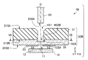
- the optical transducer 1 of this embodiment includes an optical element 10 which is a light emitting element, an optical fiber 20, and a ferrule 30.
- the optical element 10 has a light emitting surface 10SA that emits an optical signal, and a plurality of bonding electrodes 12 are arranged on the light emitting surface 10SA.
- the optical element 10 having a microscopic size of 250 ⁇ m ⁇ 250 ⁇ m in plan view has a light emitting portion 11 having a diameter of 10 ⁇ m and a plurality of bonding electrodes 12 for supplying a drive signal to the light emitting portion 11 on a light emitting surface 10SA. (Vertical Cavity Surface Emitting LASER) or light emitting diode.
- the image pickup signal output from the image pickup element 2 is converted into a drive signal for driving the optical element 10 by a drive circuit (not shown), and is input to the bonding electrode 12.
- the optical fiber 20 that transmits an optical signal has, for example, a core having a diameter of 50 ⁇ m that transmits an optical signal and a clad having a diameter of 125 ⁇ m that covers the outer periphery of the core.
- the ferrule 30 includes a first holding unit 31 and a second holding unit 32.
- maintenance part 31 has the 1st main surface 31SA and the 2nd main surface 31SB which opposes the 1st main surface 31SA.
- the second holding portion 32 has a third main surface 32SA and a fourth main surface 32SB that faces the third main surface 32SA.
- the third main surface 32SA of the second holding portion 32 is in contact with the second main surface 31SB of the first holding portion 31.
- the optical element 10 is mounted on the fourth main surface 32SB of the second holding unit 32. That is, the bonding electrode 12 of the optical element 10 is bonded to the wiring 33 of the second holding unit 32.
- the first holding part 31 is made of silicon, which is an opaque member.
- the second holding portion 32 is made of glass which is a transparent member.
- the opaque member and the transparent member may be made of resin, for example.
- the first holding portion 31 has a through hole H31.
- the second holding portion 32 has a bottomed recess H32 having an opening in the third main surface 32SA.
- the bottomed recess H32 is connected to the through hole H31.
- the end of the optical fiber 20 is inserted into the recess H32 through the through hole H31.
- the space A (three-dimensional range A) (see FIG. 7) from the four side surfaces 32SS of the second holding unit 32 to the tip of the optical fiber 20 is made of glass which is a transparent member. Therefore, the position of the front end surface 20SA of the optical fiber 20 can be confirmed from the side surface of the second holding unit 32.
- the tip surface 20SA of the optical fiber 20 is in contact with the bottom surface H32SA of the recess H32.
- the optical transmission efficiency does not significantly deteriorate as long as the length of the clearance is a predetermined length or less. That is, the front end surface of the optical fiber may be located between the bottom surface H32SA of the recess H32 and the third main surface 32SA.
- each of the through hole H31 and the recess H32 is a circle whose cross-sectional shape orthogonal to the optical axis O has a diameter of 130 ⁇ m, and the wall surface is perpendicular to the main surface.
- the inner dimension (inner diameter) of the recess H32 does not change in the depth direction.
- the depth of the through hole H31 that is, the thickness D31 of the first holding portion 31 is preferably 50 ⁇ m or more in order to hold the optical fiber 20 stably.
- the distance L from the bottom surface H32SA of the recess H32 to the fourth main surface 32SB is, for example, 10 ⁇ m or more and 100 ⁇ m or less. If the distance L is equal to or more than the above range, the second holding portion 32 is less likely to be damaged when the optical fiber 20 is inserted, and if the distance L is less than or equal to the above range, the optical signal transmission efficiency is good, and the third main surface 32SA is recessed from the concave portion.
- the distance to the bottom surface H32SA of H32 that is, the lower limit of the depth DH32 of the recess H32 is preferably 10 ⁇ m or more in order to visually recognize the front end surface 20SA from the side surface.
- the upper limit of the depth DH32 is preferably, for example, 50 ⁇ m or less in order to facilitate formation and prevent damage to the second holding portion 32.
- optical transducer 1 can confirm the distance between the tip surface 20SA of the optical fiber 20 and the light emitting unit 11 of the optical element 10, there is no fear that the transmission efficiency of the optical signal will decrease.
- the confirmation of the position of the tip surface 20SA is not limited to visual observation, and may be observed using the monitor screen of the microscope.
- a transparent resin having a refractive index matching function for preventing interface reflection may be interposed between the tip surface 20SA of the optical fiber 20 and the bottom surface H32SA of the recess H32.
- the transparent resin covering the tip surface 20SA of the optical fiber 20 also covers the outer peripheral surface near the tip surface 20SA. Therefore, the space A from the side surface 32SS of the second holding portion 32 to the tip of the optical fiber 20 is made of glass and transparent resin. Therefore, the position of the tip surface 20SA of the optical fiber 20 can be visually recognized from the side surface of the second holding unit 32.
- the ferrule 30 is manufactured by joining the first holding portion 31 in which the through hole H31 is formed and the second holding portion 32 in which the concave portion H32 is formed.
- a plurality of ferrules can be easily manufactured by cutting the bonded substrate in which the silicon substrate including the plurality of first holding portions 31 and the glass substrate including the plurality of second holding portions 32 are bonded.
- the bonding surface of the bonding substrate is a direct bonding surface or a bonding surface using a glass adhesive (for example, glass frit).
- a straight through hole having a wall surface perpendicular to the main surface and having a deep cross-section and having a deep depth is accurately formed by anisotropic etching by the Deep-RIE method (Bosch method) on the silicon substrate.
- the Deep-RIE method for example, an isotropic etching process using sulfur hexafluoride and a passivation (protection layer forming) process using a fluororesin gas are alternately repeated to form a protection layer on the sidewall.
- the bottom surface is etched while forming a film.
- the glass substrate having the recess H32 having the depth D is manufactured by, for example, a molding method using a mold.
- the shapes of the through hole H31 and the recess H32 in the direction orthogonal to the optical axis may be triangular, square, or hexagonal as long as the optical fiber 20 can be held.
- the size of the cross-sectional shape of the through hole H31 may be referred to as “inner diameter”, but when the cross-sectional shape is not circular, the size is “inner dimension”.
- the inner diameter of the recess H32 may be larger than the inner diameter of the through hole H31.
- the inner diameter of the through hole H31 is slightly larger than the outer diameter of the protective tube, and the inner diameter of the recess H32 is smaller than the outer diameter of the protective tube.
- a slightly larger ferrule may be used. Only the tip of the optical fiber 20 which is not covered with the protective tube is inserted into the recess H32.
- optical transducers and endoscopes of the embodiments and the modifications described below are similar to the optical transducer 1 and the endoscope 9 and have the same effect, and therefore components having the same functions are assigned the same reference numerals and described. Is omitted.
- the inner diameter (inner dimension) of the cross section orthogonal to the optical axis O becomes smaller from the opening surface toward the bottom surface H32SA. ing.
- the through hole H31 and the recess H32A are formed by etching the bonded substrate in which the silicon substrate and the glass substrate are bonded. Specifically, first, the through hole H31 is formed by using the anisotropic etching method of the silicon substrate.
- the glass substrate serves as an etching stop layer for anisotropic etching. Since the wall surface of the through hole H31 is perpendicular to the main surface, the inner diameter remains the same in the depth direction and is the same.
- the recess H32A is formed in the glass substrate by using the isotropic etching method.
- isotropic etching since the etching rate in the depth direction (optical axis direction) of the recess H32A is the same as the etching rate in the main surface direction (direction orthogonal to the optical axis), the recess H32A is orthogonal to the optical axis O.
- the inner diameter of the cross section is smaller toward the bottom surface H32SA.
- the optical transducer 1A is easier to manufacture than the optical transducer 1 because the ferrule 30A can be manufactured by performing anisotropic etching and then isotropic etching.
- the through hole H31 and the recess H32 have the same inner surface shape and inner diameter in the cross section orthogonal to the optical axis O.
- a part of the wall surface of the recess H32B is made of silicon 39.
- the wall surface of the recess H32B is silicon and glass, and the bottom surface of the recess H32B is glass.
- the inner surface shape of the cross section orthogonal to the optical axis O is a circle having an inner diameter LY, which is the same as the through hole H31.
- two regions facing each other across the optical axis O, which are a part of the wall surface, are made of silicon 39 instead of glass.
- the silicon 39 is also arranged inside the second holding portion 32B, and the outer peripheral shape thereof is elliptical.
- the recess H32B is formed by etching the central portion of the elliptic cylindrical projection 39A (see FIG. 9) using the DEEP-RIE method.
- the space A from the two side surfaces 32SSY of the second holding unit 32B to the tip of the optical fiber 20 is made of a transparent member containing glass.
- the space B (range B) from the two side surfaces 32SSX of the second holding unit 32B to the tip of the optical fiber 20 is made of not only a transparent member containing glass but also silicon.
- the position of the front end surface 20SA of the optical fiber 20 cannot be confirmed from the line of sight X-Eye from the side surface 32SSX.
- the position of the tip surface 20SA of the optical fiber 20 can be confirmed from the line of sight Y-Eye from the side surface 32SSY. If the position of the tip surface 20SA of the optical fiber 20 can be confirmed from at least one side surface, the optical fiber 20 can be reliably inserted to a predetermined position.
- the optical transducer 1B is easier to manufacture than the optical transducer 1 because the recess H32B can be formed continuously with the formation of the through hole H31 in one step (DEEP-RIR etching). Furthermore, since a part of the wall surface of the recess H32B is made of silicon that does not transmit an optical signal, the optical transducer 1B has less leakage light than the optical transducer 1.
- the opening of the first main surface 31SA of the through hole H31 has a tapered shape, the optical fiber 20 can be easily inserted. Also in the optical transducer 1 and the like, the opening of the through hole H31 may be tapered.
- Silicon substrate processing step A silicon substrate 31W having a first main surface 31SA and a second main surface 31SB facing the first main surface 31SA, and having a convex portion 39A on the second main surface 31SB. Is created
- a mask is provided on the first main surface 31SA of the silicon substrate 31W to cover the region to be the convex portion 39A, and etching is performed, so that the upper surface is the second main surface 31SB (first surface).
- the convex portion 39A having a flat surface parallel to the main surface 31SA) is produced.
- the convex portion 39A is an elliptic cylinder whose cross-section orthogonal to the optical axis O has a short axis length of LY and a long axis length of LX.
- a mask having an opening in a region to be the convex portion 39A is arranged, and a silicon layer is arranged by using a sputtering method or a CVD method to dispose the convex portion 39A. May be.
- the convex portion 39A is embedded in the glass substrate 32W by disposing the glass substrate 32W on the second main surface 31SB of the silicon substrate 31W.
- a glass substrate 32W having a concave portion H39 on the third main surface 32SA and a silicon substrate 31W having a convex portion 39A on the second main surface 31SB are laminated and bonded directly or by using a glass adhesive.
- the bonded substrate 30W is manufactured.
- the concave portion H39 is set so that the convex portion 39A is fitted therein.
- the glass substrate 32W having the recess H39 on the third main surface 32SA can be manufactured by, for example, a molding method using a mold or a flat glass processing (etching, sandblasting).
- the glass substrate 32W can also be manufactured by pouring the molten glass onto the first main surface 31SA of the silicon substrate 31W having the protrusions 39A, cooling the glass, and then polishing the outer surface of the glass to a predetermined thickness. .
- an etching mask 34 having an opening H34 is provided on the first main surface 31SA of the silicon substrate 31W of the bonding substrate 30W.
- the circular opening H34 is arranged at a position inscribed in the space extending the convex portion 39A in the optical axis direction, and its diameter is slightly larger than the outer diameter of the optical fiber 20.
- the through hole H31 from the first main surface 31SA to the second main surface 31SB and the recess H32B penetrating the projection 39A are continuously formed by using the DEEP-RIE method. It is formed.
- the recess H32B formed after the through hole H31 is formed is connected to the through hole H31.
- the DEEP-RIE method silicon is etched, but glass (silicon oxide) is not etched. For this reason, as shown in FIG. 12, when the concave portion H39 penetrating the convex portion 39A is formed, the bottom surface H39SA made of glass is not etched. Therefore, the depth of the concave portion H32B is the same as the height of the convex portion 39A.
- a plurality of ferrules 30B are produced by cutting the bonded substrate 30W in which the through hole H31 and the recess H39B are formed.
- Step S40> Optical Fiber Inserting Step
- the tip of the optical fiber 20 is inserted into the recess H32HB through the through hole H31.
- the optical transducer 1B can form the through hole H31 and the recess H32B in one step, it has less light leakage from the side surface 32SS and is easier to manufacture than the optical transducers 1 and 1A.
- the outer shape of the silicon 39C on the wall surface of the recess H32C of the second holding portion 32C of the ferrule 30C is a rectangular parallelepiped.
- the recess H32C and the through hole H31 of the first holding unit 31 are both circular in cross-sectional shape in the direction orthogonal to the optical axis.
- the recess H32C and the through hole H31C are inscribed in a space formed by extending the outer shape of the silicon 39C in the optical axis direction.
- the position of the front end surface 20SA of the optical fiber 20 can be confirmed from the sight lines X-Eye and Y-Eye from the four side surfaces 32SS.
- the through hole H31D of the first holding portion 31D and the recess H32D of the second holding portion 32D of the ferrule 30D have a sectional shape in the direction orthogonal to the optical axis. Both are regular hexagons.
- the outer shape of the silicon 39D on the wall surface of the recess H32D is a rectangular parallelepiped.
- the recess H32D and the through hole H31D are inscribed in the space extending the outer shape of the silicon 39D in the optical axis direction.
- the position of the front end surface 20SA of the optical fiber 20 can be confirmed if the line of sight X-Eye from the side surface 32SSX.
- the through hole of the first holding portion and the recess of the second holding portion may have a circular or polygonal inner surface shape as long as the inserted optical fiber can be stably held.
- the outer shape of silicon is not limited to the elliptic cylinder unless the wall surface of the recess is partially covered with silicon.
- the endoscope imaging device including the endoscope optical transducers 1, 1A to 1D and the image sensor 2 of the embodiment has the effects of the endoscope optical transducers 1 and 1A to 1D. There is also no.
Abstract
内視鏡用光トランスデューサ1は、光信号を発生する光素子10と、前記光信号を伝送する光ファイバ20と、第1の保持部31と第2の保持部32とを含むフェルール30と、を具備し、前記第1の保持部31は、第1の主面31SAと第2の主面31SBとを有し、貫通孔H31があり、前記第2の保持部32は、第3の主面32SAと第4の主面32SBとを有し、前記第3の主面32SAが前記第2の主面31SBと当接しており、前記第4の主面32SBに前記光素子10が実装されており、更に、前記第2の保持部32は、前記第3の主面32SAに開口を有する有底の凹部H32を有し、前記有底の凹部H32は前記貫通孔H31とつながっており、前記光ファイバ20が、前記貫通孔H31を挿通して前記凹部H32に挿入されており、前記第2の保持部32の側面32SSから前記光ファイバ20の先端までのスペースが、透明部材によって構成されている。
Description
本発明は、光素子と光ファイバとフェルールとを具備する内視鏡用光トランスデューサ、光素子と光ファイバとフェルールとを具備する内視鏡用光トランスデューサを含む内視鏡、および、光素子と光ファイバとフェルールとを具備する内視鏡用光トランスデューサの製造方法に関する。
内視鏡は、細長い挿入部の先端部に、撮像素子を有する。高品質の画像を表示するため、高画素数の撮像素子が検討されている。高画素数の撮像素子を使用すると、撮像素子から信号処理装置(プロセッサ)へ伝送する信号量が増加する。このため、電気信号による導線(電気ケーブル)を経由した電気信号伝送では、必要な信号量を伝送するために導線の線径を太くしたり、複数の導線を用いたりするため、挿入部が太くなるおそれがある。
挿入部を細径化し内視鏡を低侵襲化するには、電気信号に替えて光信号による細い光ファイバを経由した光信号伝送が好ましい。光信号伝送には、電気信号を光信号に変換する発光素子を含むE/O型の光トランスデューサ(電気-光変換器)と、光信号を電気信号に変換する受光素子を含むO/E型の光トランスデューサ(光-電気変換器)とが用いられる。光ファイバは光トランスデューサのフェルール(保持部材)の挿入孔に挿入されて固定されている。
内視鏡の挿入部の先端部に配設される光トランスデューサは、低侵襲化のため超小型である。このため、光ファイバを光トランスデューサのフェルールに挿入することは容易ではなかった。光ファイバが正しい位置に挿入されていないと、光素子と光ファイバとの間の距離が長くなり伝送効率が低下する。
国際公開第2018/037551号の図8には、透明部材で構成されているフェルールが開示されている。しかし、ガラス等の透明部材に光ファイバを挿通するための細長い孔を精度良く形成することは容易ではなかった。また、シリコンまたはセラミックからなるフェルールと比較すると、ガラスフェルールは機械的強度が高くはない。
本発明の実施形態は、信頼性および伝送効率の高い内視鏡用光トランスデューサ、信頼性が高く高品質の画像を表示する内視鏡、信頼性および伝送効率の高い内視鏡用光トランスデューサの製造方法を提供することを目的とする。
実施形態の内視鏡用光トランスデューサは、光信号を発生する光素子と、前記光信号を伝送する光ファイバと、第1の保持部と第2の保持部とを含むフェルールと、を具備し、前記第1の保持部は、第1の主面と前記第1の主面と対向する第2の主面とを有し、貫通孔があり、前記第2の保持部は、第3の主面と前記第3の主面と対向する第4の主面とを有し、前記第3の主面が前記第2の主面と当接しており、前記第4の主面に前記光素子が実装されており、更に、前記第2の保持部は、前記第3の主面に開口を有する有底の凹部を有し、前記有底の凹部は前記貫通孔とつながっており、前記光ファイバが、前記貫通孔を挿通して前記凹部に挿入されており、前記第2の保持部の側面から前記光ファイバの先端までのスペースが、透明部材によって構成されている。
実施形態の内視鏡は、内視鏡用光トランスデューサを含み、前記内視鏡用光トランスデューサは、光信号を発生する光素子と、前記光信号を伝送する光ファイバと、第1の保持部と第2の保持部とを含むフェルールと、を具備し、前記第1の保持部は、第1の主面と前記第1の主面と対向する第2の主面とを有し、貫通孔があり、前記第2の保持部は、第3の主面と前記第3の主面と対向する第4の主面とを有し、前記第3の主面が前記第2の主面と当接しており、前記第4の主面に前記光素子が実装されており、更に、前記第2の保持部は、前記第3の主面に開口を有する有底の凹部を有し、前記有底の凹部は前記貫通孔とつながっており、前記光ファイバが、前記貫通孔を挿通して前記凹部に挿入されており、前記第2の保持部の側面から前記光ファイバの先端までのスペースが、透明部材によって構成されている。
実施形態の内視鏡用光トランスデューサの製造方法は、第1の主面と前記第1の主面と対向する第2の主面とを有し、前記第2の主面に凸部のあるシリコン基板を作製するシリコン基板加工工程と、前記第2の主面にガラス基板を配設することによって、前記ガラス基板の中に前記凸部を埋め込んで接合基板を作製するガラス接合工程と、前記シリコン基板に、前記凸部を光軸方向に延長した空間に内接する貫通孔と、前記貫通孔とつながっており、前記貫通孔と内寸が同じであり、底面がガラスからなり、壁面がガラスおよびシリコンからなる凹部と、を形成するエッチング工程と、光ファイバを、前記貫通孔を挿通して前記凹部に挿入する光ファイバ挿入工程と、を具備する。
本発明の実施形態によれば、信頼性および伝送効率の高い内視鏡用光トランスデューサ、信頼性が高く高品質の画像を表示する内視鏡、信頼性および伝送効率の高い内視鏡用光トランスデューサの製造方法を提供できる。
<内視鏡>
図1に示すように実施形態の内視鏡9は、プロセッサ5Aおよびモニタ5Bと内視鏡システム6を構成している。実施形態の内視鏡用光トランスデューサ1(以下、「光トランスデューサ1」という。)は、内視鏡9に含まれている。
図1に示すように実施形態の内視鏡9は、プロセッサ5Aおよびモニタ5Bと内視鏡システム6を構成している。実施形態の内視鏡用光トランスデューサ1(以下、「光トランスデューサ1」という。)は、内視鏡9に含まれている。
内視鏡9は、挿入部3と、挿入部3の基端部に配設された把持部4と、把持部4から延設されたユニバーサルコード4Bと、ユニバーサルコード4Bの基端部に配設されたコネクタ4Cと、を具備する。挿入部3は、先端部3Aと、先端部3Aから延設された湾曲自在で先端部3Aの方向を変えるための湾曲部3Bと、湾曲部3Bから延設された軟性部3Cとを含む。光トランスデューサ1および撮像素子2は先端部3Aに配設されている。把持部4には術者が湾曲部3Bを操作するための操作部である回動するアングルノブ4Aが配設されている。
ユニバーサルコード4Bは、コネクタ4Cによってプロセッサ5Aに接続される。プロセッサ5Aは内視鏡システム6の全体を制御するとともに、撮像信号に信号処理を行い画像信号として出力する。モニタ5Bは、プロセッサ5Aが出力する画像信号を内視鏡画像として表示する。なお、内視鏡9は軟性鏡であるが、硬性鏡でもよい。また、内視鏡9は、医療用でも工業用でもよい。
内視鏡9の先端部3Aには、撮像素子2と光トランスデューサ1とが配設されている。光トランスデューサ1は、撮像素子2が出力する電気信号を光信号に変換するE/O型である。撮像素子2は、CMOSイメージセンサ、または、CCD等である。
光信号は、挿入部3を挿通する光ファイバ20を経由して把持部4に配設されたO/E型の光トランスデューサ1Xによって再び電気信号に変換され、メタル配線20Mを経由することによって伝送される。すなわち、撮像信号は、細径の挿入部3においては光ファイバ20を経由することによって伝送され、体内に挿入されず外径の制限の小さいユニバーサルコード4B内においては光ファイバ20よりも太いメタル配線20Mである信号ケーブルを経由することによって伝送される。
なお、O/E型の光トランスデューサ1Xがコネクタ4Cに配置されている場合には、光ファイバ20はユニバーサルコード4Bを挿通している。
光トランスデューサ1Xは、比較的、配置スペースが広い把持部4に配設されているが、光トランスデューサ1と同じ構成でもよい。また、把持部4に配設された光トランスデューサ1によって、撮像素子2への制御信号が光信号に変換され、先端部3Aに配設された光トランスデューサ1Xによって光信号が電気信号に変換されてもよい。
後述するように、光トランスデューサ1は信頼性および伝送効率が高い。このため、光トランスデューサ1を含む内視鏡9は信頼性が高く高品質の画像を表示する。
<第1実施形態>
図2および図3に示すように本実施形態の光トランスデューサ1は、発光素子である光素子10と光ファイバ20とフェルール30とを具備する。
図2および図3に示すように本実施形態の光トランスデューサ1は、発光素子である光素子10と光ファイバ20とフェルール30とを具備する。
なお、以下の説明において、各実施形態に基づく図面は、模式的なものであり、各部分の厚みと幅との関係、夫々の部分の厚みの比率などは現実のものとは異なることに留意すべきであり、図面の相互間においても互いの寸法の関係や比率が異なる部分が含まれている場合がある。また、一部の構成要素の図示、符号の付与を省略する場合がある。
光素子10は、光信号を出射する発光面10SAを有し、発光面10SAに複数の接合電極12が配設されている。例えば、平面視寸法が250μm×250μmと超小型の光素子10は、直径が10μmの発光部11と、発光部11に駆動信号を供給する複数の接合電極12と、を発光面10SAに有するVCSEL(Vertical Cavity Surface Emitting LASER)または発光ダイオードである。
撮像素子2が出力する撮像信号は、ドライブ回路(不図示)によって光素子10を駆動する駆動信号に変換されて、接合電極12に入力される。
光信号を伝送する光ファイバ20は、例えば、光信号を伝送する50μm径のコアと、コアの外周を覆う125μm径のクラッドとを有する。
フェルール30は、第1の保持部31と第2の保持部32とを含む。第1の保持部31は、第1の主面31SAと第1の主面31SAと対向する第2の主面31SBとを有する。第2の保持部32は、第3の主面32SAと第3の主面32SAと対向する第4の主面32SBとを有する。第2の保持部32の第3の主面32SAは、第1の保持部31の第2の主面31SBと当接している。
光素子10は第2の保持部32の第4の主面32SBに実装されている。すなわち、光素子10の接合電極12は、第2の保持部32の配線33に接合されている。
第1の保持部31は、不透明部材であるシリコンによって構成されている。一方、第2の保持部32は、透明部材であるガラスによって構成されている。不透明部材および透明部材は、例えば樹脂によって構成されていてもよい。
第1の保持部31には、貫通孔H31がある。一方、第2の保持部32は第3の主面32SAに開口を有する有底の凹部H32がある。有底の凹部H32は貫通孔H31とつながっている。
光ファイバ20は、先端が貫通孔H31を挿通して凹部H32に挿入されている。第2の保持部32の4側面32SSから光ファイバ20の先端までのスペースA(3次元範囲A)(図7参照)は透明部材であるガラスによって構成されている。このため、第2の保持部32の側面から、光ファイバ20の先端面20SAの位置が確認できる。
なお、光トランスデューサ1では、光ファイバ20の先端面20SAは凹部H32の底面H32SAと当接している。しかし、光ファイバ20の先端面20SAは凹部H32の底面H32SAとの間にすきまがあっても、すきまの長さが所定長以下であれば、光伝送効率が特に大きく劣化することはない。すなわち、光ファイバの先端面は、凹部H32の底面H32SAと第3の主面32SAとの間に位置していればよい。
例えば、貫通孔H31および凹部H32は、いずれも、光軸Oに直交する断面形状が径130μmの円であり、壁面が主面に対して垂直であるため、貫通孔H31の内寸(内径)および凹部H32の内寸(内径)は深さ方向において変化していない。
貫通孔H31の深さ、すなわち、第1の保持部31の厚さD31は、光ファイバ20を安定に保持するために、50μm以上であることが好ましい。凹部H32の底面H32SAから第4の主面32SBまでの距離Lは、例えば、10μm以上100μm以下である。距離Lが前記範囲以上であれば光ファイバ20の挿入時に第2の保持部32が破損しにくく、前記範囲以下であれば光信号の伝送効率がよい、また、第3の主面32SAから凹部H32の底面H32SAまでの距離、すなわち、凹部H32の深さDH32の下限は、側面から、先端面20SAを視認するために、例えば、10μm以上が好ましい。深さDH32の上限は、形成することが容易であること、また、第2の保持部32の破損防止のため、例えば、50μm以下が好ましい。
光トランスデューサ1は、光ファイバ20の先端面20SAと光素子10の発光部11との間の距離を確認できるため、光信号の伝送効率が低くなるおそれがない。
先端面20SAの位置の確認は、目視に限られるものではなく、顕微鏡のモニタ画面を用いて観察してもよいことは言うまでも無い。
光ファイバ20の先端面20SAと凹部H32の底面H32SAとの間に、界面反射を防止する屈折率整合機能を有する透明樹脂が介在していてもよい。
光ファイバ20の先端面20SAを覆っている透明樹脂は、先端面20SAの近傍の外周面も覆っている。このため、第2の保持部32の側面32SSから光ファイバ20の先端までのスペースAは、ガラスと透明樹脂とによって構成されている。従って、第2の保持部32の側面から、光ファイバ20の先端面20SAの位置が視認できる。
<光トランスデューサの製造方法>
図4に示すように、貫通孔H31が形成された第1の保持部31と、凹部H32が形成された第2の保持部32とが接合されることによってフェルール30は作製される。
図4に示すように、貫通孔H31が形成された第1の保持部31と、凹部H32が形成された第2の保持部32とが接合されることによってフェルール30は作製される。
複数の第1の保持部31を含むシリコン基板と、複数の第2の保持部32を含むガラス基板とが接合された接合基板の切断によって複数のフェルールを容易に作製できる。接合基板の接合面は、直接接合面またはガラス用接着剤(例えば、ガラスフリット)を用いた接着面である。
シリコン基板に、主面に対して垂直な壁面のある、断面形状が変化しない深さが深いストレート貫通孔は、Deep-RIE法(ボッシュ法)による異方性エッチングを用いて精度良く形成される。Deep-RIE法では、例えば、六フッ化硫黄を用いた等方性エッチング工程とフッ素樹脂系のガスを用いたパッシベーション(保護層形成)工程とを交互に繰り返すことによって、保護層を側壁に成膜しながら底面がエッチングされる。一方、深さDの凹部H32のあるガラス基板は、例えば、型を用いた成型法を用いて作製される。
なお、貫通孔H31および凹部H32の光軸直交方向の形状は、光ファイバ20を保持できれば、三角形、正方形または六角形でもよい。例えば貫通孔H31の断面形状の大きさを「内径」と言うことがあるが、断面形状が円形でない場合には、大きさは「内寸」となる。
なお、凹部H32の内径は、貫通孔H31の内径よりも大きくてもよい。光ファイバ20が保護チューブに覆われている場合に、貫通孔H31の内径が保護チューブの外径よりも僅かに大きく、凹部H32の内径が保護チューブの外径よりも小さく光ファイバ20の外径よりも僅かに大きいフェルールを用いてもよい。凹部H32には、保護チューブに覆われていない光ファイバ20の先端部だけが挿入される。
<第2実施形態>
以下に説明する実施形態および変形例の光トランスデューサおよび内視鏡は、光トランスデューサ1および内視鏡9と類似しており同じ効果を有するため、同じ機能の構成要素には同じ符号を付し説明は省略する。
以下に説明する実施形態および変形例の光トランスデューサおよび内視鏡は、光トランスデューサ1および内視鏡9と類似しており同じ効果を有するため、同じ機能の構成要素には同じ符号を付し説明は省略する。
図5に示す第2実施形態の光トランスデューサ1Aでは、第2の保持部32Aの凹部H32Aは、光軸Oに直交する断面形状の内径(内寸)が開口面から底面H32SAに向かって小さくなっている。
光トランスデューサ1Aのフェルール30Aは、シリコン基板とガラス基板とが接合された接合基板をエッチング処理することによって、貫通孔H31および凹部H32Aが形成される。具体的には、最初にシリコン基板の異方性エッチング法を用いて貫通孔H31が形成される。ガラス基板が異方性エッチングのエッチングストップ層となる。貫通孔H31は、壁面が主面に対して垂直であるため、内径が深さ方向において変化しておらず、同じである。
異方性エッチングの後に、等方性エッチング法を用いてガラス基板に凹部H32Aが形成される。等方性エッチングでは、凹部H32Aの深さ方向(光軸方向)のエッチング速度と、主面方向(光軸直交方向)のエッチング速度とが同じであるため、凹部H32Aは、光軸Oに直交する断面の内径が底面H32SAに向かって小さくなっている。
光トランスデューサ1Aは、異方性エッチングのあとに等方性エッチングを行うことでフェルール30Aが作製できるため、光トランスデューサ1よりも製造が容易である。
<第3実施形態>
図6および図7に示すように、本実施形態の光トランスデューサ1Bでは、貫通孔H31および凹部H32は、光軸Oに直交する断面の内面形状および内径が同じである。しかし、凹部H32Bは壁面の一部がシリコン39からなる。言い替えれば、凹部H32Bの壁面は、シリコンおよびガラスであり、凹部H32Bの底面はガラスである。
図6および図7に示すように、本実施形態の光トランスデューサ1Bでは、貫通孔H31および凹部H32は、光軸Oに直交する断面の内面形状および内径が同じである。しかし、凹部H32Bは壁面の一部がシリコン39からなる。言い替えれば、凹部H32Bの壁面は、シリコンおよびガラスであり、凹部H32Bの底面はガラスである。
すなわち、凹部H32Bは、光軸Oに直交する断面の内面形状は、内径LYの円形であり、貫通孔H31と同じである。しかし、凹部H32Bは、壁面の一部である、光軸Oをはさんで対向する2つの領域が、ガラスではなく、シリコン39からなる。
図7に示すように、光軸Oに直交する断面においては、シリコン39は第2の保持部32Bの内部にも配設されおり、その外周形状は楕円形である。後述するように、凹部H32Bは、楕円柱の凸部39A(図9参照)の中心部を、DEEP-RIE法を用いてエッチングすることによって形成されている。
光トランスデューサ1Bでは、第2の保持部32Bの2つの側面32SSYから光ファイバ20の先端までのスペースAは、ガラスを含む透明部材によって構成されている。一方、第2の保持部32Bの2つの側面32SSXから光ファイバ20の先端までのスペースB(範囲B)は、ガラスを含む透明部材だけではなく、シリコンによって構成されている。
このため、図7に示すように、側面32SSXからの視線X-Eyeでは、光ファイバ20の先端面20SAの位置は確認できない。しかし、側面32SSYからの視線Y-Eyeでは、光ファイバ20の先端面20SAの位置が確認できる。少なくとも1つの側面から光ファイバ20の先端面20SAの位置が確認できれば、光ファイバ20を確実に所定位置まで挿入できる。
1つの工程(DEEP-RIRエッチング)で、貫通孔H31の形成と連続して凹部H32Bを形成できるため、光トランスデューサ1Bは光トランスデューサ1よりも製造が容易である。さらに、凹部H32Bの壁面の一部が、光信号が透過しないシリコンであるため、光トランスデューサ1Bは光トランスデューサ1よりも、漏れ光が少ない。
なお、光トランスデューサ1Bは貫通孔H31の第1の主面31SAの開口がテーパー形状であるため、光ファイバ20の挿入が容易である。光トランスデューサ1等においても、貫通孔H31の開口がテーパー形状でもよい。
<光トランスデューサの製造方法>
図8のフローチャートに沿って光トランスデューサ1Bの製造方法を説明する。
図8のフローチャートに沿って光トランスデューサ1Bの製造方法を説明する。
<ステップS10>シリコン基板加工工程
第1の主面31SAと第1の主面31SAと対向する第2の主面31SBとを有し、第2の主面31SBに凸部39Aのあるシリコン基板31Wが作製される
第1の主面31SAと第1の主面31SAと対向する第2の主面31SBとを有し、第2の主面31SBに凸部39Aのあるシリコン基板31Wが作製される
図9に示すように、シリコン基板31Wの第1の主面31SAに、凸部39Aとなる領域を覆うマスクを配設し、エッチングを行うことで、上面が第2の主面31SB(第1の主面31SA)と平行な平面の凸部39Aが作製される。図7に示したように、凸部39Aは、光軸Oに直交する断面の形状が、短軸の長さがLY、長軸の長さがLXの楕円柱である。
第1の主面31SAに、凸部39Aとなる領域が開口となっているマスクを配設し、スパッタ法またはCVD法を用いてシリコン層を配設することによって、凸部39Aを配設してもよい。
<ステップS20>ガラス接合工程
図10に示すように、シリコン基板31Wの第2の主面31SBにガラス基板32Wを配設することによって、ガラス基板32Wの中に凸部39Aが埋め込まれる。
図10に示すように、シリコン基板31Wの第2の主面31SBにガラス基板32Wを配設することによって、ガラス基板32Wの中に凸部39Aが埋め込まれる。
例えば、第3の主面32SAに凹部H39があるガラス基板32Wと、第2の主面31SBに凸部39Aがあるシリコン基板31Wとを積層し、直接接合またはガラス用接着剤を用いて接着することによって、接合基板30Wが作製される。なお、凹部H39は、凸部39Aが嵌合する状態に設定されている。
第3の主面32SAに凹部H39があるガラス基板32Wは、例えば、型を用いた成型法、または、平板ガラスの加工(エッチング、サンドブラスト)によって作製できる。
または、シリコン基板31Wの凸部39Aがある第1の主面31SAに溶融ガラスを流し込み冷却してから、ガラスの外面を研磨し所定の厚さに加工することによっても、ガラス基板32Wは作製できる。
<ステップS30>異方性エッチング工程
図11に示すように、接合基板30Wのシリコン基板31Wの第1の主面31SAに、開口H34のあるエッチングマスク34が配設される。円形の開口H34は、凸部39Aを光軸方向に延長した空間に内接する位置に配設されており、その直径は光ファイバ20の外径よりも僅かに大きい。
図11に示すように、接合基板30Wのシリコン基板31Wの第1の主面31SAに、開口H34のあるエッチングマスク34が配設される。円形の開口H34は、凸部39Aを光軸方向に延長した空間に内接する位置に配設されており、その直径は光ファイバ20の外径よりも僅かに大きい。
エッチングマスク34を用いて、第1の主面31SAから第2の主面31SBに至る貫通孔H31と、凸部39Aを貫通している凹部H32Bと、がDEEP-RIE法を用いて連続して形成される。貫通孔H31が形成された後に、形成される凹部H32Bは、貫通孔H31とつながっている。
DEEP-RIE法では、シリコンはエッチングされるが、ガラス(酸化シリコン)はエッチングされない。このため、図12に示すように、凸部39Aを貫通する凹部H39が形成されると、ガラスからなる底面H39SAはエッチングされない。このため、凹部H32Bの深さは、凸部39Aの高さと同じである。
図示しないが、貫通孔H31および凹部H39Bが形成された接合基板30Wを切断することによって、複数のフェルール30Bが作製される。
<ステップS40>光ファイバ挿入工程
光ファイバ20の先端が、貫通孔H31を挿通して凹部H32HBに挿入される。
光ファイバ20の先端が、貫通孔H31を挿通して凹部H32HBに挿入される。
光トランスデューサ1Bは、1つの工程で貫通孔H31と凹部H32Bとを形成できるため、光トランスデューサ1、1Aよりも、側面32SSからの漏光が少なく、製造が容易である。
<第3実施形態の変形例>
図13に示す変形例1の光トランスデューサ1Cでは、フェルール30Cの第2の保持部32Cの凹部H32Cの壁面のシリコン39Cの外形は直方体である。凹部H32Cと、第1の保持部31の貫通孔H31とは光軸直交方向の断面形状が共に円形である。そして、凹部H32Cおよび貫通孔H31Cとは、シリコン39Cの外形を光軸方向に延長した空間に内接している。
図13に示す変形例1の光トランスデューサ1Cでは、フェルール30Cの第2の保持部32Cの凹部H32Cの壁面のシリコン39Cの外形は直方体である。凹部H32Cと、第1の保持部31の貫通孔H31とは光軸直交方向の断面形状が共に円形である。そして、凹部H32Cおよび貫通孔H31Cとは、シリコン39Cの外形を光軸方向に延長した空間に内接している。
光トランスデューサ1Cでは、4側面32SSからの視線X-Eye、Y-Eyeから、光ファイバ20の先端面20SAの位置が確認できる。
図14に示す変形例2の光トランスデューサ1Dでは、フェルール30Dの、第1の保持部31Dの貫通孔H31Dと、第2の保持部32Dの凹部H32Dと、は、光軸直交方向の断面形状が共に正六角形である。凹部H32Dの壁面のシリコン39Dの外形は直方体である。そして、凹部H32Dおよび貫通孔H31Dとは、シリコン39Dの外形を光軸方向に延長した空間に内接している。
光トランスデューサ1Dでは、側面32SSXからの視線X-Eyeであれば、光ファイバ20の先端面20SAの位置が確認できる。
以上の変形例のように、第1の保持部の貫通孔および第2の保持部の凹部は、挿入された光ファイバを安定に保持できれば、その内面形状は円形でも多角柱でもよい。また、凹部は壁面の一部がシリコンで覆われていなければ、シリコンの外形形状は楕円柱に限られるものではない。
また、実施形態の内視鏡用光トランスデューサ1、1A~1Dと撮像素子2とを含む内視鏡用撮像装置が、内視鏡用光トランスデューサ1、1A~1Dの効果を有することは言うまでも無い。
本発明は、上述した各実施例に限定されるものではなく、発明の趣旨を逸脱しない範囲内において種々の変更、組み合わせ、および応用が可能である。
1、1A~1D・・・内視鏡用光トランスデューサ
2・・・撮像素子
6・・・内視鏡システム
9・・・内視鏡
10・・・光素子
10SA・・・発光面
11・・・発光部
12・・・接合電極
20・・・光ファイバ
20SA・・・先端面
20M・・・メタル配線
30・・・フェルール
30W・・・接合基板
31・・・第1の保持部
31SA・・・第1の主面
31SB・・・第2の主面
31W・・・シリコン基板
32・・・第2の保持部
32SA・・・第3の主面
32SB・・・第4の主面
32SS・・・側面
32W・・・ガラス基板
33・・・配線
34・・・エッチングマスク
39・・・シリコン
39A・・・凸部
2・・・撮像素子
6・・・内視鏡システム
9・・・内視鏡
10・・・光素子
10SA・・・発光面
11・・・発光部
12・・・接合電極
20・・・光ファイバ
20SA・・・先端面
20M・・・メタル配線
30・・・フェルール
30W・・・接合基板
31・・・第1の保持部
31SA・・・第1の主面
31SB・・・第2の主面
31W・・・シリコン基板
32・・・第2の保持部
32SA・・・第3の主面
32SB・・・第4の主面
32SS・・・側面
32W・・・ガラス基板
33・・・配線
34・・・エッチングマスク
39・・・シリコン
39A・・・凸部
Claims (9)
- 光信号を発生する光素子と、
前記光信号を伝送する光ファイバと、
第1の保持部と第2の保持部とを含むフェルールと、を具備し
前記第1の保持部は、第1の主面と前記第1の主面と対向する第2の主面とを有し、貫通孔があり、
前記第2の保持部は、第3の主面と前記第3の主面と対向する第4の主面とを有し、前記第3の主面が前記第2の主面と当接しており、前記第4の主面に前記光素子が実装されており、
更に、前記第2の保持部は、前記第3の主面に開口を有する有底の凹部があり、前記有底の凹部は前記貫通孔とつながっており、
前記光ファイバが、前記貫通孔を挿通して前記凹部に挿入されており、
前記第2の保持部の側面から前記光ファイバの先端までのスペースが、透明部材によって構成されていることを特徴とする内視鏡用光トランスデューサ。 - 前記第1の保持部はシリコンによって構成され、前記第2の保持部はガラスによって構成されることを特徴とする請求項1に記載の内視鏡用光トランスデューサ。
- 前記光ファイバの先端面が、前記凹部の底面と前記第3の主面との間に位置していることを特徴とする請求項1または2に記載の内視鏡用光トランスデューサ。
- 前記凹部の内寸が底面に向かって小さくなっていることを特徴とする請求項1から請求項3のいずれか1項に記載の内視鏡用光トランスデューサ。
- 前記貫通孔の内寸および前記凹部の内寸は、同じで、ともに深さ方向において変化しておらず、
前記第2の保持部は、前記凹部の壁面がシリコンおよびガラスからなることを特徴とする請求項1から請求項3のいずれか1項に記載の内視鏡用光トランスデューサ。 - 前記壁面の一部である、光軸をはさんで対向する2つの領域が、シリコンからなることを特徴とする請求項5に記載の内視鏡用光トランスデューサ。
- 請求項1から請求項6のいずれか1項に記載の光トランスデューサを含むことを特徴とする内視鏡。
- 第1の主面と前記第1の主面と対向する第2の主面とを有し、前記第2の主面に凸部のあるシリコン基板を作製するシリコン基板加工工程と、
前記第2の主面にガラス基板を配設することによって、前記ガラス基板の中に前記凸部を埋め込んで接合基板を作製するガラス接合工程と、
前記シリコン基板に、前記凸部を光軸方向に延長した空間に内接する貫通孔と、前記貫通孔とつながっており、前記貫通孔と内寸が同じであり、底面がガラスからなり、壁面がガラスおよびシリコンからなる凹部と、を形成するエッチング工程と、
光ファイバを、前記貫通孔を挿通して前記凹部に挿入する光ファイバ挿入工程と、を具備することを特徴とする内視鏡用光トランスデューサの製造方法。 - 前記エッチング工程が、前記貫通孔と前記凹部とを連続してエッチングするDEEP-RIE法による異方性エッチング工程であることを特徴とする請求項8に記載の内視鏡用光トランスデューサの製造方法。
Priority Applications (2)
| Application Number | Priority Date | Filing Date | Title |
|---|---|---|---|
| PCT/JP2018/038500 WO2020079754A1 (ja) | 2018-10-16 | 2018-10-16 | 内視鏡用光トランスデューサ、内視鏡、および内視鏡用光トランスデューサの製造方法 |
| US17/225,295 US20210251471A1 (en) | 2018-10-16 | 2021-04-08 | Optical transducer for endoscope, endoscope, and manufacturing method of optical transducer for endoscope |
Applications Claiming Priority (1)
| Application Number | Priority Date | Filing Date | Title |
|---|---|---|---|
| PCT/JP2018/038500 WO2020079754A1 (ja) | 2018-10-16 | 2018-10-16 | 内視鏡用光トランスデューサ、内視鏡、および内視鏡用光トランスデューサの製造方法 |
Related Child Applications (1)
| Application Number | Title | Priority Date | Filing Date |
|---|---|---|---|
| US17/225,295 Continuation US20210251471A1 (en) | 2018-10-16 | 2021-04-08 | Optical transducer for endoscope, endoscope, and manufacturing method of optical transducer for endoscope |
Publications (1)
| Publication Number | Publication Date |
|---|---|
| WO2020079754A1 true WO2020079754A1 (ja) | 2020-04-23 |
Family
ID=70283746
Family Applications (1)
| Application Number | Title | Priority Date | Filing Date |
|---|---|---|---|
| PCT/JP2018/038500 WO2020079754A1 (ja) | 2018-10-16 | 2018-10-16 | 内視鏡用光トランスデューサ、内視鏡、および内視鏡用光トランスデューサの製造方法 |
Country Status (2)
| Country | Link |
|---|---|
| US (1) | US20210251471A1 (ja) |
| WO (1) | WO2020079754A1 (ja) |
Citations (3)
| Publication number | Priority date | Publication date | Assignee | Title |
|---|---|---|---|---|
| WO2015150149A1 (en) * | 2014-03-31 | 2015-10-08 | Koninklijke Philips N.V. | Optical connector for sterile applications |
| WO2016189691A1 (ja) * | 2015-05-27 | 2016-12-01 | オリンパス株式会社 | 内視鏡および光伝送モジュール |
| WO2018150512A1 (ja) * | 2017-02-16 | 2018-08-23 | オリンパス株式会社 | 光モジュール、内視鏡、および、光モジュールの製造方法 |
Family Cites Families (3)
| Publication number | Priority date | Publication date | Assignee | Title |
|---|---|---|---|---|
| JP6411088B2 (ja) * | 2013-09-26 | 2018-10-24 | オリンパス株式会社 | 光伝送モジュールおよび内視鏡 |
| JP2015097588A (ja) * | 2013-11-18 | 2015-05-28 | オリンパス株式会社 | 光伝送モジュール及び内視鏡 |
| KR102349774B1 (ko) * | 2015-03-11 | 2022-01-10 | 삼성전자주식회사 | 광전 회로 |
-
2018
- 2018-10-16 WO PCT/JP2018/038500 patent/WO2020079754A1/ja active Application Filing
-
2021
- 2021-04-08 US US17/225,295 patent/US20210251471A1/en active Pending
Patent Citations (3)
| Publication number | Priority date | Publication date | Assignee | Title |
|---|---|---|---|---|
| WO2015150149A1 (en) * | 2014-03-31 | 2015-10-08 | Koninklijke Philips N.V. | Optical connector for sterile applications |
| WO2016189691A1 (ja) * | 2015-05-27 | 2016-12-01 | オリンパス株式会社 | 内視鏡および光伝送モジュール |
| WO2018150512A1 (ja) * | 2017-02-16 | 2018-08-23 | オリンパス株式会社 | 光モジュール、内視鏡、および、光モジュールの製造方法 |
Also Published As
| Publication number | Publication date |
|---|---|
| US20210251471A1 (en) | 2021-08-19 |
Similar Documents
| Publication | Publication Date | Title |
|---|---|---|
| JP6411088B2 (ja) | 光伝送モジュールおよび内視鏡 | |
| EP2134236B1 (en) | Compact scanning fiber device | |
| US9232197B2 (en) | Endoscope apparatus and method for releasing heat generated by imaging element of the endoscope apparatus | |
| WO2018173323A1 (ja) | 内視鏡 | |
| WO2016117120A1 (ja) | 撮像装置および内視鏡 | |
| US10972707B2 (en) | Endoscope and method of manufacturing endoscope | |
| WO2015045630A1 (ja) | 撮像モジュールおよび内視鏡装置 | |
| US20190384013A1 (en) | Optical module, endoscope and manufacturing method of optical module | |
| JP6203010B2 (ja) | 内視鏡 | |
| WO2016189691A1 (ja) | 内視鏡および光伝送モジュール | |
| JP6485840B2 (ja) | 光伝送モジュールおよび内視鏡 | |
| JP6043032B2 (ja) | 内視鏡 | |
| WO2019208633A1 (ja) | 内視鏡用光モジュール、内視鏡、および内視鏡用光モジュールの製造方法 | |
| WO2020079754A1 (ja) | 内視鏡用光トランスデューサ、内視鏡、および内視鏡用光トランスデューサの製造方法 | |
| JP6602970B2 (ja) | 光信号送信モジュール | |
| JP6502475B2 (ja) | 光伝送モジュール、撮像装置および光伝送モジュール用構造体 | |
| WO2018139406A1 (ja) | 内視鏡および内視鏡の製造方法 | |
| JPS63136781A (ja) | 固体撮像装置 | |
| WO2020089969A1 (ja) | 内視鏡用光トランスデューサ、内視鏡、および、内視鏡用光トランスデューサの製造方法 | |
| US20210382250A1 (en) | Manufacturing method for image pickup apparatus for endoscope, image pickup apparatus for endoscope, and endoscope | |
| WO2017072862A1 (ja) | 撮像ユニットおよび内視鏡 | |
| US11846808B2 (en) | Optical transducer for endoscope, endoscope, and manufacturing method for optical transducer for endoscope | |
| US11918179B2 (en) | Image pickup apparatus for endoscope, endoscope, and manufacturing method for image pickup apparatus for endoscope | |
| WO2018146806A1 (ja) | 光モジュールおよび内視鏡 | |
| WO2020178972A1 (ja) | 内視鏡用光トランスデューサ、内視鏡、および内視鏡用光トランスデューサの製造方法 |
Legal Events
| Date | Code | Title | Description |
|---|---|---|---|
| 121 | Ep: the epo has been informed by wipo that ep was designated in this application |
Ref document number: 18937509 Country of ref document: EP Kind code of ref document: A1 |
|
| NENP | Non-entry into the national phase |
Ref country code: DE |
|
| 122 | Ep: pct application non-entry in european phase |
Ref document number: 18937509 Country of ref document: EP Kind code of ref document: A1 |
|
| NENP | Non-entry into the national phase |
Ref country code: JP |