WO2020071379A1 - ハードコート層付高分子基板 - Google Patents
ハードコート層付高分子基板Info
- Publication number
- WO2020071379A1 WO2020071379A1 PCT/JP2019/038783 JP2019038783W WO2020071379A1 WO 2020071379 A1 WO2020071379 A1 WO 2020071379A1 JP 2019038783 W JP2019038783 W JP 2019038783W WO 2020071379 A1 WO2020071379 A1 WO 2020071379A1
- Authority
- WO
- WIPO (PCT)
- Prior art keywords
- layer
- group
- silicon oxide
- range
- oxide layer
- Prior art date
- Legal status (The legal status is an assumption and is not a legal conclusion. Google has not performed a legal analysis and makes no representation as to the accuracy of the status listed.)
- Ceased
Links
Images


Classifications
-
- B—PERFORMING OPERATIONS; TRANSPORTING
- B32—LAYERED PRODUCTS
- B32B—LAYERED PRODUCTS, i.e. PRODUCTS BUILT-UP OF STRATA OF FLAT OR NON-FLAT, e.g. CELLULAR OR HONEYCOMB, FORM
- B32B27/00—Layered products comprising a layer of synthetic resin
-
- B—PERFORMING OPERATIONS; TRANSPORTING
- B32—LAYERED PRODUCTS
- B32B—LAYERED PRODUCTS, i.e. PRODUCTS BUILT-UP OF STRATA OF FLAT OR NON-FLAT, e.g. CELLULAR OR HONEYCOMB, FORM
- B32B27/00—Layered products comprising a layer of synthetic resin
- B32B27/30—Layered products comprising a layer of synthetic resin comprising vinyl (co)polymers; comprising acrylic (co)polymers
-
- B—PERFORMING OPERATIONS; TRANSPORTING
- B32—LAYERED PRODUCTS
- B32B—LAYERED PRODUCTS, i.e. PRODUCTS BUILT-UP OF STRATA OF FLAT OR NON-FLAT, e.g. CELLULAR OR HONEYCOMB, FORM
- B32B9/00—Layered products comprising a layer of a particular substance not covered by groups B32B11/00 - B32B29/00
-
- C—CHEMISTRY; METALLURGY
- C08—ORGANIC MACROMOLECULAR COMPOUNDS; THEIR PREPARATION OR CHEMICAL WORKING-UP; COMPOSITIONS BASED THEREON
- C08J—WORKING-UP; GENERAL PROCESSES OF COMPOUNDING; AFTER-TREATMENT NOT COVERED BY SUBCLASSES C08B, C08C, C08F, C08G or C08H
- C08J7/00—Chemical treatment or coating of shaped articles made of macromolecular substances
- C08J7/04—Coating
-
- C—CHEMISTRY; METALLURGY
- C09—DYES; PAINTS; POLISHES; NATURAL RESINS; ADHESIVES; COMPOSITIONS NOT OTHERWISE PROVIDED FOR; APPLICATIONS OF MATERIALS NOT OTHERWISE PROVIDED FOR
- C09D—COATING COMPOSITIONS, e.g. PAINTS, VARNISHES OR LACQUERS; FILLING PASTES; CHEMICAL PAINT OR INK REMOVERS; INKS; CORRECTING FLUIDS; WOODSTAINS; PASTES OR SOLIDS FOR COLOURING OR PRINTING; USE OF MATERIALS THEREFOR
- C09D183/00—Coating compositions based on macromolecular compounds obtained by reactions forming in the main chain of the macromolecule a linkage containing silicon, with or without sulfur, nitrogen, oxygen, or carbon only; Coating compositions based on derivatives of such polymers
- C09D183/10—Block or graft copolymers containing polysiloxane sequences
-
- C—CHEMISTRY; METALLURGY
- C09—DYES; PAINTS; POLISHES; NATURAL RESINS; ADHESIVES; COMPOSITIONS NOT OTHERWISE PROVIDED FOR; APPLICATIONS OF MATERIALS NOT OTHERWISE PROVIDED FOR
- C09D—COATING COMPOSITIONS, e.g. PAINTS, VARNISHES OR LACQUERS; FILLING PASTES; CHEMICAL PAINT OR INK REMOVERS; INKS; CORRECTING FLUIDS; WOODSTAINS; PASTES OR SOLIDS FOR COLOURING OR PRINTING; USE OF MATERIALS THEREFOR
- C09D5/00—Coating compositions, e.g. paints, varnishes or lacquers, characterised by their physical nature or the effects produced; Filling pastes
-
- C—CHEMISTRY; METALLURGY
- C09—DYES; PAINTS; POLISHES; NATURAL RESINS; ADHESIVES; COMPOSITIONS NOT OTHERWISE PROVIDED FOR; APPLICATIONS OF MATERIALS NOT OTHERWISE PROVIDED FOR
- C09D—COATING COMPOSITIONS, e.g. PAINTS, VARNISHES OR LACQUERS; FILLING PASTES; CHEMICAL PAINT OR INK REMOVERS; INKS; CORRECTING FLUIDS; WOODSTAINS; PASTES OR SOLIDS FOR COLOURING OR PRINTING; USE OF MATERIALS THEREFOR
- C09D7/00—Features of coating compositions, not provided for in group C09D5/00; Processes for incorporating ingredients in coating compositions
- C09D7/40—Additives
- C09D7/60—Additives non-macromolecular
- C09D7/61—Additives non-macromolecular inorganic
-
- B—PERFORMING OPERATIONS; TRANSPORTING
- B60—VEHICLES IN GENERAL
- B60J—WINDOWS, WINDSCREENS, NON-FIXED ROOFS, DOORS, OR SIMILAR DEVICES FOR VEHICLES; REMOVABLE EXTERNAL PROTECTIVE COVERINGS SPECIALLY ADAPTED FOR VEHICLES
- B60J1/00—Windows; Windscreens; Accessories therefor
Definitions
- the present invention relates to a polymer substrate provided with a hard coat layer.
- the present invention relates to a polymer substrate with a hard coat layer that has excellent wear resistance, weather resistance, high hardness, and heat resistance and can be used for a long period of time even under severe use environments.
- This polymer substrate with a hard coat layer can be used, for example, for automotive window materials, building members, surface protection plates for solar cells, and the like.
- resin moldings with high transparency are superior to inorganic glass in lightness, impact resistance, workability, formability with surrounding parts, design, etc. Taking advantage of these advantages, they have been widely used in various applications instead of inorganic glass.
- these resins are inferior in surface abrasion resistance and hardness compared to inorganic glass, so they may be used as polymer substrates with hard coat layers in the form of laminated hard coat layers to prevent damage. Many.
- polymer substrates with a hard coat layer for automotive windows have the mechanical strength required for window materials and the same abrasion resistance as inorganic glass to ensure visibility in driving safety.
- environmental resistance that can withstand long-term outdoor exposure.
- environmental resistance it has the ability to pass various tests assuming direct contact with moisture such as rainy weather, use in high humidity / dry environment, high / low temperature conditions, strong UV exposure, etc. There is a need. It can be said that the above proposals are still insufficient as a resin glazing material capable of stably achieving all of these required performances.
- the abrasion resistance equivalent to inorganic glass for example, referring to standards such as the North American safety standard FMVSS205 and the European safety standard ECE R43, the abrasion resistance of windows used in parts that require visibility during operation
- the property requirement is that the haze value increase ( ⁇ H) by a Taber abrasion test at 1000 rpm specified in ASTM D1044 is less than 2% or less than 2%.
- boiling water resistance Resistance to the boiling water test (hereinafter referred to as boiling water resistance), which is an accelerated test for direct contact with moisture in the operating environment and long-term storage in a high-humidity environment, and high-temperature durability, which is an accelerated test for temperature changes in the operating environment Resistance to the test (hereinafter referred to as heat resistance) was often insufficient, and defects such as poor adhesion of the high-hardness hard coat layer, peeling phenomena, and crack generation were often observed.
- thermosetting film of an acrylic resin, a thermosetting film of an organosiloxane resin, and a PE-CVD film using an organic silicon compound as a raw material are sequentially laminated on at least one surface of a plastic substrate.
- the PE-CVD film has a gradient zone in which the abundance ratio of oxygen atoms and silicon atoms (O / Si ratio) increases from the interface with the thermosetting film of the organosiloxane resin and a substantially constant gradient zone following the gradient zone.
- a plastic laminate comprising a flat zone is proposed.
- Examples 1 and 2 include Taber abrasion performance of 2.0% or less and boiling water resistance by a boiling water immersion test of 2 hours, which are the targets of the present invention.
- a laminate having both heat resistance at 1000C for 1000 hours is disclosed.
- the immersion time in boiling water is 2 hours, but in order to ensure sufficient long-term reliability such as water resistance and moisture resistance, the immersion time in boiling water is at least 3 hours, more preferably 4 hours or more. I found that things were good.
- the evaluation method of the adhesion test after immersion in boiling water it was found that the evaluation immediately after the test by the cross-cut tape method was insufficient, and it was necessary to confirm the evaluation at least 7 days after the test was performed. This is because the internal stress (compressive force in many cases) generated during the formation of the layer often remains in the silicon oxide layer formed by the PE-CVD method, and this action causes the separation of the layer over time. Was found to be seen.
- a polymer substrate with a hard coat layer was immersed in boiling water at 100 ° C., kept for 3 hours, taken out of the boiling water, removed adhering water, left standing at room temperature for 2 hours, and compliant with JIS K5400.
- An adhesion test is performed by a crosscut tape method.
- a square having 10 ⁇ 10 cuts was formed into a cross-cut shape at 1 mm intervals with a cutter knife, and then a tape having a predetermined adhesive strength (for example, Nichiban Cellotape (trademark)) was attached and fixed. It is done in a form to be peeled off later.
- Adhesion results immediately after the cross-cut tape test are referred to as “initial results”, and the results after 7 days from the cross-cut tape test are performed are “time-lapse results”. Only when the “time result” was also good, the adhesion performance and its reliability were determined to be good.
- the “initial result” was good (100/100).
- the hard coat layer was peeled off by the CVD method. That is, in the case of Example 1, the evaluation result was 70/100 (layer peeling occurred in 30 out of 100 squares), and in the case of Example 2, the result was 0/100 (layer peeling occurred in all 100 squares). The results were not satisfactory, and the performance needed to be improved.
- infrared reflection technology and infrared absorption technology as the technology to cut off the infrared rays.
- Infrared absorption technology among them can suppress the rise in the temperature inside the car, but the window itself becomes extremely hot. I will.
- Patent Document 2 discloses a silicone coating composition
- a silicone coating composition comprising an outermost layer (I) formed by plasma-polymerizing an organic silicon compound on an organic resin substrate, a composite oxide fine particle dispersion, a silicone resin, a curing catalyst, and a solvent.
- a laminate having a plurality of coating layers including a lower layer (II) and optionally a lower layer (III) of an acrylic resin is proposed.
- the target of the present invention is 2% or less.
- a laminate having Taber abrasion performance is disclosed. It also discloses the correlation between individual physical properties and performance of each layer constituting the laminate.
- Patent Document 3 a substrate, a first layer of a partial condensate of an organosiloxane, and plasma-polymerized organosilicon are deposited at a power level of 10 6 to 10 8 J / Kg under excess oxygen.
- a multilayer product comprising a second layer is proposed, and Example 2 discloses the results of good appearance (no minute cracks) and good adhesion after a one-year outdoor exposure test in Florida, USA.
- Nos. 4 and 5 disclose results of good appearance (no minute cracks) and good adhesion after a xenon weather-accelerated weathering test with an integrated radiation dose of 6875 KJ / m 2 .
- Patent Document 4 a cured underlayer containing a hydrolysis-condensation product of an organic silicon compound as a main component and a PE-CVD method of an organic silicon compound are formed on the surface of a polymer substrate.
- a polymer substrate with a hard coat in which a silicon oxide layer satisfying specific requirements is laminated has been proposed, and it has been disclosed that the heat resistance at 110 ° C. for 1000 hours was good, and that excellent boiling water resistance and weather resistance were obtained. Have been.
- Patent Document 5 discloses a laminate in which a cured coating layer (I) of an active energy ray-curable primer composition and an inorganic material layer (II) are sequentially laminated on a resin substrate,
- the line-curable primer composition is (A) a silsesquioxane compound having an organic group directly bonded to a silicon atom, and at least one of the organic groups is an organic group having a (meth) acryloyloxy group.
- a structure containing a silsesquioxane compound and (B) a photopolymerization initiator wherein the inorganic material layer (II) is formed by a dry film formation method.
- Patent Document 6 a first hard coat layer made of an ultraviolet-curable resin, an anchor coat layer made of an organic-inorganic hybrid resin, and an organic silicon-based or organic aluminum-based reaction gas during chemical vapor deposition are applied to a base film. And a second hard coat layer having high scratch resistance obtained by forming a film using the same.
- Patent Document 7 discloses an organic resin base material and a multilayer coating layer on the surface of the base material, wherein the multilayer coating layer is the outermost layer of a hard coating obtained by plasma-polymerizing an organic silicon compound ( I) and an intermediate layer (II) of a cured film formed from the composite coating composition (2), wherein one surface of the intermediate layer (II) is in contact with the outermost layer and the other surface is in contact with the organic resin base material.
- (2) inorganic oxide nanoparticles comprising (2-A) one selected from silica, zinc oxide, titanium oxide, cerium oxide, and a combination comprising at least one of the foregoing.
- (2-B) a vinyl copolymer having an organic ultraviolet absorbing group and a reactive group selected from an alkoxysilyl group, a hydroxyl group, an epoxy group, a carboxylic acid group and an amino group, and (2-B) ) Contains a solvent, organic resin laminate is disclosed having a weather resistance and scratch resistance.
- Patent Document 8 discloses a laminate in which a resin layer (I) of an active energy ray-curable resin composition and an inorganic oxide vapor-deposited film layer (II) are provided in this order. There is disclosed a laminate characterized in that the resin composition contains a composite resin used in the cured underlayer of the present invention.
- the present invention relates to a polymer substrate with a hard coat layer having a hard layer formed by laminating a high-hardness hard coat layer by a plasma-induced chemical vapor deposition (PE-CVD) method on the surface layer.
- PE-CVD plasma-induced chemical vapor deposition
- the present invention is as follows with respect to solving the above-mentioned problems.
- the cured underlayer has a thickness of 1 to 20 ⁇ m and contains 10 to 90 parts by weight of a polyfunctional acrylate, 90 to 10 parts by weight of inorganic oxide fine particles and / or a hydrolyzed condensate of a silicon compound.
- a condensate is an essential component
- the silicon compound hydrolytic condensate has a structural unit represented by the general formula (1) and / or the general formula (2) and a silanol group and / or a hydrolyzable silyl group.
- R 4 is Represents a single bond or an alkylene group having 1 to 6 carbon atoms), an alkyl group having 1 to 6 carbon atoms, a cycloalkyl group having 3 to 8 carbon atoms, an aryl group, or an aralkyl having 7 to 12 carbon atoms.
- R 1 , R 2 and R 3 is a group having the above-mentioned polymerizable double bond
- a carbon atom forms a part of the vinyl polymer segment (a2)
- a silicon atom bonded only to an oxygen atom forms a part of the polysiloxane segment (a1).
- the silicon oxide layer satisfies all of the following requirements (a 1 ) to (c 1 ) at a position of 0.04 ⁇ m in the thickness direction from the interface between the hardened base layer and the silicon oxide layer, and Satisfies all of the following requirements (b 3 ) to (c 3 ) on the surface opposite to Polymer substrate with hard coat layer according to ⁇ 1>:
- (A 1 ) When the chemical composition is represented by SiO x C y H z , x is in the range of 1.93 to 1.98, y is in the range of 0.04 to 0.15, and z is Being in the range of 0.10 to 0.45,
- (B 1) IR absorbance ratio of the wave number 930 cm -1 and 1020cm -1 ( ⁇ 930 / ⁇ 1020 ) may be in the range of 0.10-0.20,
- (C 1) IR absorbance ratio of the wave number 1280 cm -1 and 1020cm -1 ( ⁇ 1280 / ⁇ 1020 ) may be in the range
- y in (a 3 ) is larger by 0.02 to 0.10 than y in (a 1 ), and z in (a 3 ) is 0.05 more than z in (a 1 ).
- the base cured layer contains a (meth) acrylic resin containing 0.1 to 5 mol / kg of at least one selected from a hydroxyl group, an amino group, a carboxyl group and an alkoxysilyl group in a compound.
- ⁇ 5> The polymer substrate with a hard coat layer according to any one of ⁇ 1> to ⁇ 4>, wherein the inorganic oxide fine particles have a primary particle size of 1 nm to 200 nm.
- ⁇ 6> The polymer substrate with a hard coat layer according to any one of ⁇ 1> to ⁇ 5>, wherein the polymer substrate is a polycarbonate resin substrate.
- ⁇ 7> The polymer substrate with a hard coat layer according to any one of ⁇ 1> to ⁇ 6>, wherein the silicon oxide layer is a plasma CVD layer.
- the silicon oxide layer has a thickness of 2.5 to 9 ⁇ m, and the following (a 2 ) to (c 2 ) are located at 2.0 ⁇ m in the thickness direction from the interface between the hardened underlayer and the silicon oxide layer.
- the polymer substrate with a hard coat layer according to any one of ⁇ 1> to ⁇ 7>, which satisfies all the requirements of (1):
- (A 2 ) When the chemical composition is represented by SiO x C y H z , x is in the range of 1.81 to 1.90, y is in the range of 0.15 to 0.32, and z is In the range of 0.45 to 0.90,
- B 2 Infrared absorbance ratio of the wave number 930 cm -1 and 1020cm -1 ( ⁇ 930 / ⁇ 1020 ) may be in the range of 0.21 to 0.36,
- (C 2) Infrared absorbance ratio of the wave number 1280 cm -1 and 1020cm -1 ( ⁇ 1280 / ⁇ 1020 ) may be
- ⁇ 12> Between a portion of the silicon oxide layer satisfying all the requirements (a 2 ) to (c 2 ) and a portion of the silicon oxide layer satisfying all the requirements of (a 3 ) to (c 3 ) ⁇ 8> further includes a gradient layer in which the change in the value of the x, the y, the z, the ⁇ 930 / ⁇ 1020 , and / or the ⁇ 1280 / ⁇ 1020 is gradient.
- ⁇ 13> The polymer substrate with a hard coat layer according to any one of ⁇ 1> to ⁇ 7>, wherein the thickness of the silicon oxide layer is 0.1 to 2.5 ⁇ m.
- FIG. 1 is a schematic view of an example of a capacitively coupled PE-CVD apparatus that can be used for forming a silicon oxide layer by the PE-CVD method of the present invention.
- FIG. 2 is a schematic view of another example of a capacitive coupling type PE-CVD apparatus that can be used for forming a silicon oxide layer by the PE-CVD method of the present invention.
- FIG. 3A is an example of a reactive gas introduction head provided on an electrode in a capacitively coupled PE-CVD apparatus that can be used for forming a silicon oxide layer by the PE-CVD method of the present invention, and
- FIG. b) shows an arrangement (an example) of a large number of gas ejection holes provided on the surface facing the substrate to be processed.
- 1 is a schematic cross-sectional view of a polymer substrate with a hard coat layer applied to one embodiment of the present invention. It is a cross section of a polymer substrate with a hard coat layer applied to another embodiment of the present invention.
- an under-cured layer 70 and a silicon oxide layer 80 formed by PE-CVD are laminated in this order on at least one surface of the polymer substrate 50.
- lamination of the layer on the other side is not always essential, and a preferable configuration is selected according to the application and necessity.
- another layer may not be present on the other surface of the polymer substrate 50.
- a layer other than the adhesive layer 60, the underlying cured layer 70, and the silicon oxide layer 80 by PE-CVD for example, an ultraviolet curable resin layer). , Etc.
- Polymer substrate 50 examples of the material of the polymer substrate 50 include acrylic resins such as polycarbonate resin and polymethyl methacrylate, polyester resins such as polyethylene terephthalate, polybutylene terephthalate, and poly (ethylene-2,6-naphthalate), polystyrene resins, polypropylene resins, and polyarylate. Resin, polyethersulfone resin, ABS resin, polylactic acid resin, and the like. These resins can be used alone or in combination of two or more. Among these, polycarbonate resins having excellent transparency, heat resistance, impact resistance, and the like are particularly preferable when used for automobile windows. More preferably, the polymer substrate is an acrylic-coated polycarbonate substrate coextruded with an acrylic resin for covering the surface together with the polycarbonate resin.
- the heat distortion temperature (HDT) is preferably 100 ° C. or higher, more preferably 120 ° C. or higher, and further preferably 130 ° C. or higher.
- the polycarbonate resin is, for example, a polycarbonate resin obtained by reacting a dihydric phenol with a carbonate precursor by an interfacial polycondensation method or a melting method.
- the dihydric phenol include 2,2-bis (4-hydroxyphenyl) propane (commonly known as bisphenol A), 2,2-bis (3-methyl-4-hydroxyphenyl) propane, 2-bis (3,5-dimethyl-4-hydroxyphenyl) propane, 1,1-bis (4-hydroxyphenyl) ethane, 1,1-bis (4-hydroxyphenyl) cyclohexane, 2,2-bis (4 -Hydroxyphenyl) butane, 2,2-bis (4-hydroxyphenyl) -3-methylbutane, 9,9-bis ⁇ (4-hydroxy-3-methyl) phenyl ⁇ fluorene, 2,2-bis (4-hydroxy Phenyl) -3,3-dimethylbutane, 2,2-bis (4-hydroxyphenyl) -4-methylpentane, 1,1
- carbonate precursor carbonyl halide, carbonate ester or haloformate
- specific examples include phosgene, diphenyl carbonate, dihaloformate of dihydric phenol and the like.
- a catalyst, a terminal stopper, an antioxidant for a dihydric phenol, and the like may be used as necessary. May be used.
- the polycarbonate resin may be a branched polycarbonate resin obtained by copolymerizing a trifunctional or higher polyfunctional aromatic compound, or a polyester carbonate resin obtained by copolymerizing an aromatic or aliphatic bifunctional carboxylic acid, Further, a mixture of two or more of the obtained polycarbonate resins may be used.
- the molecular weight of the polycarbonate resin is preferably 10,000 to 50,000, more preferably 15,000 to 35,000 in terms of viscosity average molecular weight (M).
- M viscosity average molecular weight
- a polycarbonate resin having such a viscosity average molecular weight is preferable because sufficient strength is obtained and the melt fluidity during molding is good.
- the viscosity average molecular weight referred to in the present invention is determined by inserting the specific viscosity ( ⁇ sp ) obtained from a solution obtained by dissolving 0.7 g of a polycarbonate resin in 100 ml of methylene chloride at 20 ° C. into the following equation.
- polycarbonate resin examples include various copolymerized polycarbonates such as a polycarbonate resin obtained by copolymerizing isosorbide and an aliphatic diol, and a polycarbonate-polyorganosiloxane copolymer.
- Such a polycarbonate resin may include, if necessary, a stabilizer such as a phosphite, a phosphate or a phosphonate, a low molecular weight polycarbonate such as tetrabromobisphenol A, a tetrabromobisphenol A, a flame retardant such as decabromodiphenol, a benzotriazole.
- a stabilizer such as a phosphite, a phosphate or a phosphonate
- a low molecular weight polycarbonate such as tetrabromobisphenol A, a tetrabromobisphenol A
- a flame retardant such as decabromodiphenol, a benzotriazole.
- UV absorbers such as benzophenones, triazines and salicylates; inorganic UV absorbers such as titanium oxide, cerium oxide and zinc oxide; cyanine compounds, squalilium compounds, thiol nickel complex salt compounds, phthalocyanine compounds Compounds, triallylmethane compounds, naphthoquinone compounds, anthraquinone compounds, carbon black, antimony oxide, tin oxide doped with indium oxide, infrared shielding agents such as lanthanum boride, coloring agents, lubricants, etc. Combined and can be used.
- the thickness of the polymer substrate is preferably in the range of 1 to 20 mm. If the thickness is less than 1 mm, it is difficult to maintain the required mechanical strength of window materials for automobiles and the like, and the lamination of the silicon oxide layer by the PE-CVD method increases the flexural deformation of the substrate, causing problems in dimensional stability and appearance. This often occurs and is not preferred. On the other hand, when the thickness is more than 20 mm, it is difficult to obtain a molded substrate having surface smoothness required as a window material and having small optical distortion (such as perspective distortion), and the substrate weight is increased. Not preferred.
- the thickness of the polymer substrate is more preferably 2 to 10 mm, and still more preferably 3 to 7 mm.
- the base cured layer 70 of the first embodiment is laminated on the surface of the polymer substrate, contains a silicon compound hydrolyzed condensate, and the silicon compound hydrolyzed condensate is formed by the general formula (1) and / or
- the polysiloxane segment (a1) having a structural unit represented by the general formula (2), a silanol group and / or a hydrolyzable silyl group, and the vinyl polymer segment (a2) are formed by the general formula ( It contains the composite resin (A) bound by the bond represented by 3) and has a thickness of 1 to 20 ⁇ m. This thickness may be, for example, 1 ⁇ m or more, 3 ⁇ m or more, 5 ⁇ m or more, and may be 20 ⁇ m or less, 15 ⁇ m or less, or 10 ⁇ m or less.
- the underlayer cured layer (70) is composed of 10 to 90 parts by weight of a polyfunctional acrylate having two or more (meth) acryloyl groups in one molecule, and the sum of any inorganic oxide fine particles and a silicon compound hydrolyzed condensate. It is preferably a layer obtained by heat curing or active energy ray curing of a precursor composition containing 90 to 10 parts by weight (hereinafter, referred to as a precursor composition), particularly a layer obtained by active energy ray curing. Is preferred.
- (meth) acrylate refers to one or both of acrylate and methacrylate
- (meth) acryloyl group refers to one or both of an acryloyl group and a methacryloyl group.
- Examples of the optionally used polyfunctional (meth) acrylate include trimethylolpropane di (meth) acrylate, ethylene oxide-modified trimethylolpropane di (meth) acrylate, propylene oxide-modified trimethylolpropane di (meth) acrylate, and glycerin diacrylate.
- (meth) acrylates can be used, but it is preferable to use two or more of them in combination to balance hardness and flexibility. Further, among these (meth) acrylates, it is preferable that pentaerythritol tri (meth) acrylate and pentaerythritol tetra (meth) acrylate are blended in a certain amount to improve the scratch resistance.
- the inorganic oxide fine particles optionally used for example, titanium oxide, zinc oxide, cerium oxide, silicon oxide and the like can be mentioned.
- the primary particle size of the inorganic oxide fine particles is preferably 1 nm to 200 nm, more preferably 1 nm to 100 nm. The above range is preferable because a cured underlayer having excellent transparency and weather resistance can be formed.
- the silicon compound hydrolyzed condensate is a polysiloxane segment (a1) having a structural unit represented by the general formula (1) and / or the general formula (2) and a silanol group and / or a hydrolyzable silyl group. (Hereinafter simply referred to as a polysiloxane segment (a1)) and a vinyl polymer segment (a2) (hereinafter simply referred to as a vinyl polymer segment (a2)) represented by the general formula (3). Containing the composite resin (A) bonded by Here, the polysiloxane segment (a1) is an essential component of the structural unit represented by the general formula (1) and / or the general formula (2), but the vinyl polymer segment (a2) is also an essential component. And the structural unit represented by the general formula (1) and / or the general formula (2). Examples of the composite resin (A) include resins described in paragraphs 0035 to 0087 of Patent Document 8. This document is incorporated by reference.
- the base cured layer 70 may be substantially composed of only a silicon compound hydrolyzed condensate containing the composite resin (A). It is preferably composed of a functional acrylate, and more preferably contains a composite resin (A), a polyfunctional acrylate, and inorganic oxide fine particles.
- the composite resin (A) used in the present invention is a polysiloxane having a structural unit represented by the general formula (1) and / or the general formula (2) and a silanol group and / or a hydrolyzable silyl group.
- the bond represented by the general formula (3) has hydrolysis resistance and is excellent in long-term weather resistance.
- a dehydration condensation reaction occurs between a silanol group and / or a hydrolyzable silyl group of the polysiloxane segment (a1) described below and a silanol group and / or a hydrolyzable silyl group of the vinyl polymer segment (a2) described later.
- the bond represented by the general formula (3) is generated. Therefore, in the general formula (3), carbon atoms constitute a part of the vinyl polymer segment (a2), and silicon atoms bonded only to oxygen atoms constitute a part of the polysiloxane segment (a1).
- Examples of the form of the composite resin (A) include a composite resin having a graft structure in which the polysiloxane segment (a1) is chemically bonded as a side chain of the polymer segment (a2), or the polymer segment (a2). And the above-mentioned polysiloxane segment (a1).
- the polysiloxane segment (a1) in the present invention is a segment having a structural unit represented by the general formula (1) and / or the general formula (2) and a silanol group and / or a hydrolyzable silyl group.
- the structural unit represented by the general formula (1) and / or the general formula (2) contains a group having a polymerizable double bond.
- the structural unit represented by the general formula (1) and / or the general formula (2) has a group having a polymerizable double bond as an essential component.
- R 1 , R 2 and R 3 is a group having the above-mentioned polymerizable double bond.
- the alkylene group having 1 to 6 carbon atoms for R 4 include a methylene group, an ethylene group, a propylene group, an isopropylene group, a butylene group, an isobutylene group, a sec-butylene group, a tert-butylene group, Pentylene group, isopentylene group, neopentylene group, tert-pentylene group, 1-methylbutylene group, 2-methylbutylene group, 1,2-dimethylpropylene group, 1-ethylpropylene group, hexylene group, isohexylene group, 1-methylpentylene Benzene, 2-methylpentylene, 3-methylpentylene, 1,1-dimethylbutylene, 1,2-dimethylbutylene, 2,2-dimethyl
- the alkyl group having 1 to 6 carbon atoms includes, for example, methyl group, ethyl group, propyl group, isopropyl group, butyl group, isobutyl group, sec-butyl group, tert-butyl group, pentyl group, isopentyl Group, neopentyl group, tert-pentyl group, 1-methylbutyl group, 2-methylbutyl group, 1,2-dimethylpropyl group, 1-ethylpropyl group, hexyl group, isohexyl group, 1-methylpentyl group, 2-methylpentyl Group, 3-methylpentyl group, 1,1-dimethylbutyl group, 1,2-dimethylbutyl group, 2,2-dimethylbutyl group, 1-ethylbutyl group, 1,1,2-trimethylpropyl group, 1,2 , 2-trimethylpropyl group, 1-ethyl-2-methylpropyl group, 1-ethy
- Examples of the cycloalkyl group having 3 to 8 carbon atoms include a cyclopropyl group, a cyclobutyl group, a cyclopentyl group, and a cyclohexyl group.
- Examples of the aryl group include a phenyl group, a naphthyl group, a 2-methylphenyl group, a 3-methylphenyl group, a 4-methylphenyl group, a 4-vinylphenyl group, and a 3-isopropylphenyl group.
- Examples of the aralkyl group having 7 to 12 carbon atoms include a benzyl group, a diphenylmethyl group, and a naphthylmethyl group.
- R 1 , R 2 and R 3 are a group having a polymerizable double bond
- the polysiloxane segment (a1) is represented by the general formula (1) when having the structural unit is a group R 1 has a polymerizable double bond
- having the structural unit of polysiloxane segment (a1) is represented by the general formula (2) R 2 and And / or when R 3 is a group having a polymerizable double bond and the polysiloxane segment (a1) has both the structural units represented by the general formulas (1) and (2), It shows that at least one of 1 , R 2 and R 3 is a group having a polymerizable double bond.
- two or more polymerizable double bonds are preferably present in the polysiloxane segment (a1), more preferably 3 to 200, and still more preferably 3 to 50.
- a coating film having excellent durability can be obtained.
- the content of the polymerizable double bond in the polysiloxane segment (a1) is 3 to 35% by weight, desired weather resistance and adhesion can be obtained.
- the term "polymerizable double bond" as used herein is a general term for a vinyl group, a vinylidene group or a vinylene group capable of performing a growth reaction by a free radical.
- the content of the polymerizable double bond indicates the weight% of the vinyl group, vinylidene group or vinylene group in the polysiloxane segment.
- the group having a polymerizable double bond all known functional groups containing the vinyl group, vinylidene group and vinylene group can be used.
- the structural unit represented by the general formula (1) and / or the general formula (2) is a three-dimensional network-like polysiloxane structural unit in which two or three of the silicon bonds are involved in crosslinking. Since a dense network structure is not formed even though a three-dimensional network structure is formed, gelation or the like does not occur during production or formation of a primer, and storage stability is improved.
- the silanol group is a silicon-containing group having a hydroxyl group directly bonded to a silicon atom.
- the silanol group is a silanol group formed by bonding an oxygen atom having a bond to a hydrogen atom in the structural unit represented by the general formula (1) and / or the general formula (2).
- the hydrolyzable silyl group is a silicon-containing group having a hydrolyzable group directly bonded to a silicon atom, and specifically includes, for example, a group represented by the general formula (4). .
- R 5 represents a monovalent organic group such as an alkyl group, an aryl group or an aralkyl group
- R 6 represents a halogen atom, an alkoxy group, an acyloxy group, a phenoxy group, an aryloxy group, a mercapto group
- the alkyl group include a methyl group, an ethyl group, a propyl group, an isopropyl group, butyl group, isobutyl group, sec- butyl group, tert- butyl group, a pentyl group, isopentyl group, neopentyl group, tert -Pentyl, 1-methylbutyl, 2-methylbutyl, 1,2-dimethylpropyl, 1-ethylpropyl, hexyl, isohexyl, 1-methylpentyl, 2-methylpentyl, 3-methylpentyl Group, 1,1-dimethylbutyl group, 1,2-dimethylbutyl group, 2,2-dimethylbutyl group, 1-ethylbutyl group, 1,1,2-trimethylpropyl group, 1,2,2-trimethylpropyl group , 1-ethyl-2-methylpropyl group, 1-ethyl-1-methylpropyl group and the
- Examples of the aryl group include a phenyl group, a naphthyl group, a 2-methylphenyl group, a 3-methylphenyl group, a 4-methylphenyl group, a 4-vinylphenyl group, and a 3-isopropylphenyl group.
- Examples of the aralkyl group include a benzyl group, a diphenylmethyl group, and a naphthylmethyl group.
- the halogen atom e.g., fluorine atom, chlorine atom, bromine atom, and an iodine atom.
- the alkoxy group include a methoxy group, an ethoxy group, a propoxy group, an isopropoxy group, a butoxy group, a second butoxy group, and a tertiary butoxy group.
- the acyloxy group include, for example, formyloxy, acetoxy, propanoyloxy, butanoyloxy, pivaloyloxy, pentanoyloxy, phenylacetoxy, acetoacetoxy, benzoyloxy, naphthoyloxy and the like.
- Examples of the aryloxy group include phenyloxy and naphthyloxy.
- Examples of the alkenyloxy group include a vinyloxy group, an allyloxy group, a 1-propenyloxy group, an isopropenyloxy group, a 2-butenyloxy group, a 3-butenyloxy group, a 2-petenyloxy group, a 3-methyl-3-butenyloxy group, -Hexenyloxy group and the like.
- the hydrolyzable silyl group represented by the general formula (4) becomes a silanol group.
- a methoxy group and an ethoxy group are preferable because of excellent hydrolyzability.
- the hydrolyzable silyl group is formed by bonding an oxygen atom having a bond of the structural unit represented by the general formula (1) and / or the general formula (2) to the hydrolyzable group.
- it is preferably a substituted hydrolyzable silyl group.
- the silanol group or the hydrolyzable silyl group is formed by a curing reaction of the group having a polymerizable double bond, a hydroxyl group or a hydrolyzable silyl group in the silanol group is formed in parallel with the curing reaction. Since the hydrolysis-condensation reaction proceeds between the hydrolyzable groups in the group, the crosslink density of the polysiloxane structure of the resulting coating film increases, and a coating film having excellent solvent resistance and the like can be formed. Further, the polysiloxane segment (a1) containing the silanol group or the hydrolyzable silyl group and the vinyl polymer segment (a2) described below are bonded via a bond represented by the general formula (3). Used when
- the polysiloxane segment (a1) is not particularly limited except that it has a structural unit represented by the general formula (1) and / or the general formula (2) and a silanol group and / or a hydrolyzable silyl group. , And may contain other groups.
- Polysiloxanes R 1 in the general formula (1) is a structural unit is a group having a polymerizable double bond
- R 1 in the general formula (1) coexist and the structural unit is an alkyl group such as methyl It may be a segment (a1)
- a structural unit R 1 is an alkyl group such as a methyl group and structural units R 1 is a group having a polymerizable double bond in the formula (1)
- R 2 and R 3 in may be a polysiloxane segments coexist a structural unit is an alkyl group such as a methyl group (a1)
- the structural unit in which R 1 in the general formula (1) is a group having the polymerizable double bond and the structural unit in which R 2 and R 3 in the general formula (2) are an alkyl group such as a methyl group are included.
- the coexisting polysiloxane segment (a1) may be used, and there is no particular limitation. Specifically, examples of the polysiloxan
- the polysiloxane segment (a1) preferably contains 10 to 65% by weight based on the total solid content of the active energy ray-curable resin composition constituting the resin layer (I). It is possible to achieve both the adhesion to the material and the inorganic oxide vapor-deposited film layer (II) and the weather resistance.
- the vinyl polymer segment (a2) in the present invention is a vinyl polymer segment such as an acrylic polymer, a fluoroolefin polymer, a vinyl ester polymer, an aromatic vinyl polymer, and a polyolefin polymer.
- an acrylic polymer segment is preferred because the resulting coating film is excellent in transparency and gloss.
- the acrylic polymerizable segment is obtained by polymerizing or copolymerizing a general-purpose (meth) acrylic monomer.
- the (meth) acrylic monomer is not particularly limited, and a vinyl monomer can also be copolymerized.
- the vinyl polymer segment (a2) in the present invention is more preferably a (meth) acrylic repeating unit having a cyclic hydrocarbon group from the viewpoint of improving adhesion to a plastic substrate.
- the (meth) acrylic repeating unit having a cyclic hydrocarbon group preferably, cyclohexyl (meth) acrylate, cyclopentanyl (meth) acrylate, adamantyl (meth) acrylate, tricyclodecanyl (meth) acrylate, tetracyclododecanyl ( (Meth) acrylates having a cyclic hydrocarbon group, such as (meth) acrylate, dicyclopentanyl (meth) acrylate, and isobornyl acrylate. These can be used alone or in combination of two or more.
- the vinyl polymer segment (a2) can be obtained by a known method.
- 2,2′-azobis (isobutyronitrile), 2,2′-azobis (2,4-) are obtained by various polymerization methods such as bulk radical polymerization, solution radical polymerization, and non-aqueous dispersion radical polymerization.
- the vinyl polymer segment (a2) can be obtained by using a polymerization initiator such as tert-butyl peroxide, cumene hydroperoxide, diisopropyl peroxycarbonate.
- the number average molecular weight of the vinyl polymer segment (a2) is preferably in the range of 500 to 200,000 in terms of number average molecular weight (hereinafter abbreviated as Mn), and the composite resin (A) is produced. It is possible to prevent thickening and gelation at the time of performing, and it is excellent in durability. Mn is more preferably in the range of 700 to 100,000, and still more preferably in the range of 1,000 to 50,000 in view of the suitability for coating and adhesion to the substrate described below.
- the vinyl-based polymer segment (a2) is a vinyl-based polymer segment (a) in order to form a composite resin (A) bonded to the polysiloxane segment (a1) by a bond represented by the general formula (3). It has a silanol group and / or a hydrolyzable silyl group directly bonded to a carbon bond in a2). Since these silanol groups and / or hydrolyzable silyl groups become bonds represented by the general formula (3) in the production of the composite resin (A) described below, the composite resin (A )) Hardly exists in the vinyl polymer segment (a2).
- the vinyl-based polymer segment (a2) having a silanol group and / or a hydrolyzable silyl group directly bonded to a carbon bond is, specifically, the general-purpose monomer and the silanol group and / or directly bonded to a carbon bond. It is obtained by copolymerizing with a vinyl monomer containing a hydrolyzable silyl group.
- Examples of the vinyl monomer having a silanol group and / or a hydrolyzable silyl group directly bonded to a carbon bond include vinyltrimethoxysilane, vinyltriethoxysilane, vinylmethyldimethoxysilane, and vinyltri (2-methoxyethoxy) silane.
- the vinyl polymer segment (a2) preferably has an alcoholic hydroxyl group.
- the vinyl polymer segment (a2) having an alcoholic hydroxyl group can be obtained by copolymerizing a (meth) acrylic monomer having an alcoholic hydroxyl group.
- Specific examples of the (meth) acrylic monomer having an alcohol hydroxyl group include 2-hydroxyethyl (meth) acrylate, 2-hydroxypropyl (meth) acrylate, 3-hydroxypropyl (meth) acrylate, and 2-hydroxybutyl (meth) acrylate.
- the amount of the alcoholic hydroxyl group is appropriately determined by calculating from the amount of polyisocyanate (B) to be described later. Further, as described later, in the present invention, it is more preferable to use an active energy ray-curable monomer having an alcoholic hydroxyl group in combination. Therefore, the amount of the alcoholic hydroxyl group in the vinyl polymer segment (a2) having an alcoholic hydroxyl group can be determined in consideration of the amount of the active energy ray-curable monomer having an alcoholic hydroxyl group used in combination. It is preferable that the content is substantially in the range of 30 to 300 in terms of the hydroxyl value of the vinyl polymer segment (a2).
- the composite resin (A) used in the present invention is specifically produced by the following (method 1) to (method 3).
- Method 1 The general-purpose (meth) acrylic monomer or the like and the vinyl-based monomer having a silanol group and / or a hydrolyzable silyl group directly bonded to the carbon bond are copolymerized to directly bond to the carbon bond.
- a vinyl polymer segment (a2) containing a silanol group and / or a hydrolyzable silyl group is obtained.
- This is mixed with a silane compound having both a silanol group and / or a hydrolyzable silyl group and a polymerizable double bond and, if necessary, a general-purpose silane compound, and subjected to a hydrolysis-condensation reaction.
- a silanol group and / or a hydrolyzable silyl group and a silanol group or a hydrolyzable silyl group of a silane compound having a polymerizable double bond are combined with a silanol group and / or a hydrolyzable group directly bonded to a carbon bond.
- the silanol group and / or the hydrolyzable silyl group of the vinyl polymer segment (a2) containing a hydrophilic silyl group undergoes a hydrolysis-condensation reaction to form the polysiloxane segment (a1) and the polysiloxane.
- the composite resin (A) in which the segment (a1) and the vinyl polymer segment (a2) are composited by the bond represented by the general formula (3) is obtained.
- Method 2 In the same manner as in Method 1, a vinyl polymer segment (a2) containing a silanol group and / or a hydrolyzable silyl group directly bonded to a carbon bond is obtained.
- a silane compound having both a silanol group and / or a hydrolyzable silyl group and a polymerizable double bond and, if necessary, a general-purpose silane compound are subjected to a hydrolytic condensation reaction to obtain a polysiloxane segment (a1).
- Method 3 In the same manner as in Method 1, a vinyl polymer segment (a2) containing a silanol group and / or a hydrolyzable silyl group directly bonded to a carbon bond is obtained. On the other hand, in the same manner as in Method 2, a polysiloxane segment (a1) is obtained. Further, a silane compound containing a silane compound having a polymerizable double bond and, if necessary, a general-purpose silane compound are mixed and subjected to a hydrolytic condensation reaction.
- Examples of the silane compound having a silanol group and / or a hydrolyzable silyl group and a polymerizable double bond used in the above-mentioned (method 1) to (method 3) include, specifically, vinyltrimethoxysilane, Vinyltriethoxysilane, vinylmethyldimethoxysilane, vinyltri (2-methoxyethoxy) silane, vinyltriacetoxysilane, vinyltrichlorosilane, 2-trimethoxysilylethylvinylether, 3- (meth) acryloyloxypropyltrimethoxysilane, 3- (Meth) acryloyloxypropyltriethoxysilane, 3- (meth) acryloyloxypropylmethyldimethoxysilane, 3- (meth) acryloyloxypropyltrichlorosilane and the like can be mentioned. Among them, vinyltrimethoxysilane and 3- (meth) acryloyloxyprop
- Examples of general-purpose silane compounds used in (Method 1) to (Method 3) include, for example, methyltrimethoxysilane, methyltriethoxysilane, methyltri-n-butoxysilane, ethyltrimethoxysilane, n-propyl
- organotrialkoxysilanes such as trimethoxysilane, iso-butyltrimethoxysilane, cyclohexyltrimethoxysilane, phenyltrimethoxysilane, phenyltriethoxysilane; dimethyldimethoxysilane, dimethyldiethoxysilane, dimethyldi-n-butoxysilane
- Diorganodialkoxysilanes such as dimethyldimethoxysilane, diphenyldimethoxysilane, methylcyclohexyldimethoxysilane or methylphenyldimethoxysilane; methylt
- a tetrafunctional alkoxysilane compound such as tetramethoxysilane, tetraethoxysilane or tetra-n-propoxysilane or a partially hydrolyzed condensate of the tetrafunctional alkoxysilane compound may be used in combination as long as the effects of the present invention are not impaired. it can.
- the silicon atoms of the tetrafunctional alkoxysilane compound are 20% of the total silicon atoms constituting the polysiloxane segment (a1). It is preferable to use them together so as not to exceed the mol%.
- a metal alkoxide compound other than a silicon atom such as boron, titanium, zirconium or aluminum can be used in combination with the silane compound as long as the effects of the present invention are not impaired.
- a metal alkoxide compound in combination with the above metal alkoxide compound in an amount not exceeding 25 mol% with respect to all silicon atoms constituting the polysiloxane segment (a1).
- a part of the hydrolyzable group is hydrolyzed under the influence of water or the like to form a hydroxyl group, and then the hydroxyl groups are hydrolyzed with each other or with the hydroxyl group. It refers to a progressing condensation reaction that progresses with an ionic group.
- the hydrolysis-condensation reaction can be carried out by a known method, but a method in which the reaction is carried out by supplying water and a catalyst in the production step is simple and preferable.
- the catalyst to be used examples include: inorganic acids such as hydrochloric acid, sulfuric acid and phosphoric acid; organic acids such as p-toluenesulfonic acid, monoisopropyl phosphate and acetic acid; inorganic bases such as sodium hydroxide and potassium hydroxide; tetraisopropyl titanate And titanates such as tetrabutyl titanate; 1,8-diazabicyclo [5.4.0] undecene-7 (DBU), 1,5-diazabicyclo [4.3.0] nonene-5 (DBN), Compounds containing various basic nitrogen atoms, such as 1,4-diazabicyclo [2.2.2] octane (DABCO), tri-n-butylamine, dimethylbenzylamine, monoethanolamine, imidazole and 1-methylimidazole; Tetramethyl ammonium salt, tetrabutyl ammonium salt, dilauryl dimethyl ammonium Various quaternary am
- the amount of the catalyst to be added is not particularly limited, but it is generally preferable to use the catalyst in an amount of 0.0001 to 10% by weight based on the total amount of each of the compounds having a silanol group or a hydrolyzable silyl group. , More preferably in the range of 0.0005 to 3% by weight, and particularly preferably in the range of 0.001 to 1% by weight.
- the amount of water to be supplied is preferably 0.05 mol or more, and more preferably 0.1 mol, per 1 mol of the silanol group or the hydrolyzable silyl group of each compound having the silanol group or the hydrolyzable silyl group.
- the above is more preferable, and particularly preferably 0.5 mol or more.
- These catalyst and water may be supplied collectively or sequentially, or a mixture of the catalyst and water in advance may be supplied.
- the reaction temperature for performing the hydrolysis-condensation reaction in the above (Method 1) to (Method 3) is suitably in the range of 0 ° C to 150 ° C, preferably in the range of 20 ° C to 100 ° C. Further, the reaction can be carried out under any conditions of normal pressure, increased pressure or reduced pressure. In addition, alcohol and water, which are by-products generated in the hydrolysis and condensation reaction, may be removed by a method such as distillation as needed.
- the charge ratio of each compound in (Method 1) to (Method 3) is appropriately selected depending on the desired structure of the composite resin (A) used in the present invention. Above all, it is preferable to obtain the composite resin (A) so that the content of the polysiloxane segment (a1) is 30 to 95% by weight because the durability of the obtained coating film is excellent, and 30 to 75% by weight is preferable. More preferred.
- the vinyl polymer segment is examples of the method include a method in which a silanol group and / or a hydrolyzable silyl group of the polysiloxane segment and a silanol group and / or a hydrolyzable silyl group of the polysiloxane segment described above are subjected to a hydrolytic condensation reaction.
- the cured undercoat layer prepared in this manner is subjected to subsequent surface treatment such as plasma treatment (atmospheric pressure, vacuum), flame treatment, corona treatment, UV (150 to 400 nm) (ozone) treatment, chemical treatment, and the like.
- plasma treatment atmospheric pressure, vacuum
- flame treatment corona treatment
- UV (150 to 400 nm) (ozone) treatment UV (150 to 400 nm) (ozone) treatment
- chemical treatment and the like.
- Part of the components decomposes and disappears, and the proportion of the inorganic components increases inclining toward the surface, achieving an extremely good surface to ensure adhesion to the silicon oxide layer by PE-CVD. it can.
- the surface of the under-cured layer has a water contact angle of 35 ° or less, and the surface roughness when measured by a DFM method under an observation condition of 5 ⁇ m square.
- Ra is preferably in the range of 0.7 to 10.0 nm. Since the underlying hardened layer also often becomes electrically insulating, the DFM method is effective for observing the surface thereof, as described later.
- the water contact angle reflects the magnitude of the intermolecular force with the polar substance on the polymer substrate surface.
- liquid such as water on a solid surface becomes a sphere because the surface area is reduced if there is no intermolecular force with the surface, but if intermolecular force (surface energy) acts between the solid surface and water, water becomes It spreads on the solid surface in order to obtain and stabilize more surface energy, and the contact angle is reduced.
- intermolecular force surface energy
- the silicon oxide layer formed by the PE-CVD method is also a layer having a high polarity, a large amount of surface energy is obtained and stabilized from a solid surface having a low water contact angle.
- a water contact angle of 35 ° or less on the substrate surface of the present invention is preferable because sufficient adhesion to the silicon oxide layer can be obtained.
- the surface roughness measured by the DFM method reflects the surface smoothness at the nano-size level of the surface of the base hardened layer, but the surface roughness is not sufficient for enhancing the adhesion to the silicon oxide layer by the PE-CVD method. It is preferable that an appropriate shape of the surface irregularities defined in the preferable range exists. Surface irregularities refer to those observed by the DFM method as single or interconnected pores and / or projections. The presence of these surface irregularities enhances the anchor effect (wedge effect) related to the improvement of adhesion. It is considered to be.
- the surface roughness (Ra) of the base cured layer surface of the present invention is less than 0.7 nm, the effect of improving the adhesion is hardly obtained.
- the surface roughness (Ra) exceeds 10.0 nm, the mechanical strength of the base cured layer surface is reduced, and as a result, In some cases, this may lead to a decrease in adhesion, which is not preferable.
- the surface roughness (Ra) of the surface of the base cured layer is in the range of 1.0 to 5.0 nm.
- the measurement by the DFM method is preferably performed under the condition of an observation area of 5 ⁇ m square, 256 ⁇ 256 measurement points, and the measurement is preferably performed in a plurality of regions, and the average value is preferably obtained.
- photopolymerization initiators examples include those shown in the following (a) to (d). These may be used alone or in combination of two or more.
- xanthones such as xanthone, thioxanthone, 2-methylthioxanthone, 2-chlorothioxanthone and 2,4-diethylthioxanthone; thioxanthones; various acyloin ethers such as benzoin, benzoin methyl ether, benzoin ethyl ether and benzoin isopropyl ether;
- (C) ⁇ -diketones such as benzyl and diacetyl; sulfides such as tetramethylthiuram disulfide and p-tolyl disulfide; various benzoic acids such as 4-dimethylaminobenzoic acid and ethyl 4-dimethylaminobenzoate;
- photopolymerization initiators 1-hydroxycyclohexylphenyl ketone, 2-hydroxy-2-methyl-1-phenylpropan-1-one, 1- [4- (2-hydroxyethoxy) phenyl] -2-hydroxy- 2-methyl-1-propan-1-one, thioxanthone and thioxanthone derivatives, 2,2′-dimethoxy-1,2-diphenylethan-1-one, 2,4,6-trimethylbenzoyldiphenylphosphine oxide, bis (2 , 4,6-trimethylbenzoyl) phenylphosphine oxide, 2-methyl-1- [4- (methylthio) phenyl] -2-morpholino-1-propanone, 2-benzyl-2-dimethylamino-1- (4-morpholino
- One or more mixed systems selected from the group of phenyl) -butan-1-ones It allows more active against a broad range of wavelengths of light is preferred because highly curable coating is obtained using.
- the amount of the photopolymerization initiator used is an amount capable of sufficiently exhibiting the function as a photopolymerization initiator, and is preferably in a range in which precipitation of crystals and deterioration of physical properties of the coating film do not occur, and specifically, It is preferably used in the range of 0.05 to 20 parts by mass, particularly preferably in the range of 0.1 to 10 parts by mass, based on 100 parts by mass of the resin composition.
- the resin composition of the present invention may further use various photosensitizers in combination with the photopolymerization initiator.
- the photosensitizer include amines, ureas, sulfur-containing compounds, phosphorus-containing compounds, chlorine-containing compounds, nitriles, and other nitrogen-containing compounds.
- An ultraviolet absorber, a solvent, and the like are further added to the coating agent for a cured underlayer of the present invention, if necessary.
- the ultraviolet absorber any of organic and inorganic ultraviolet absorbers can be used.
- the organic ultraviolet absorber include 2- [4- ⁇ (2-hydroxy-3-dodecyloxypropyl) oxy ⁇ -2- Hydroxyphenyl] -4,6-bis (2,4-dimethylphenyl) -1,3,5-triazine, 2- [4- ⁇ (2-hydroxy-3-tridecyloxypropyl) oxy ⁇ -2-hydroxy Phenyl] -4,6-bis (2,4-dimethylphenyl) -1,3,5-triazine and the like, 2- (2′-xanthencarboxy-5′-methylphenyl) benzotriazole, 2- ( 2'-o-nitrobenzyloxy-5'-methylphenyl) benzotriazole, 2-xanthencarboxy-4-dodecyloxy
- examples of the inorganic ultraviolet absorber include metal oxide fine particles such as titanium oxide, zinc oxide, and cerium oxide.
- a triazine-based ultraviolet absorber is particularly preferably used in terms of the intensity and wavelength of ultraviolet absorption, the difficulty of decomposition, and the difficulty of elution.
- the solvent is not particularly limited as long as it has affinity for both the (meth) acrylic resin and the inorganic fine particles in the coating agent, and the following solvents can be mentioned.
- Ether solvents such as ethyl ether, isopropyl ether, n-butyl ether, diisoamyl ether, ethylene glycol dimethyl ether, ethylene glycol diethyl ether, diethylene glycol dimethyl ether, diethylene glycol, dioxane, and tetrahydrofuran.
- Alcohol solvents such as methanol, ethanol, isopropyl alcohol, n-butyl alcohol, isobutyl alcohol, diacetone alcohol, 3-methoxy-1-propanol, 3-methoxy-1-butanol, 3-methyl-3-methoxybutanol;
- Hydrocarbon solvents such as toluene, xylene, Solvesso 100, Solvesso 150, Swazol 1800, Swazol 310, Isopar E, Isopar G, Exxon Naphtha 5, Exxon Naphtha 6, etc.
- the thickness of the cured layer is preferably in the range of 1 to 20 ⁇ m, more preferably 2 to 15 ⁇ m, still more preferably 3 to 10 ⁇ m, and most preferably 4 to 10 ⁇ m.
- the thickness is less than 1 ⁇ m, the thickness is insufficient to absorb the difference in the coefficient of linear expansion between the silicon oxide layer and the silicon oxide layer formed by the PE-CVD method.
- the thickness exceeds 20 ⁇ m, cracks occur in the layer due to the stress caused by the curing shrinkage of the layer, or the base layer increases in temperature due to the difference in linear expansion coefficient between the base layer and the silicon oxide layer. Since the silicon oxide layer cooperates to suppress the expansion of the underlayer, the underlayer may have wavy marks.
- the surface of the hardened underlayer immediately before the silicon oxide layer is laminated by the PE-CVD method. For example, a method of performing a plasma treatment on the substrate.
- Plasma treatment refers to a process in which gas species and electrons imparted with high kinetic energy by plasma excitation collide with the surface of the underlying hardened layer, and activates the surface of the underlying hardened layer (expression of active groups due to chemical bonding or cleavage of the crosslinked structure). ) Or etching of a surface layer portion having a low crosslink density can be performed.
- a high-frequency electromagnetic field 13.56 MHz or the like is applied to generate plasma.
- the main control parameters of the plasma processing are gas type, gas pressure or flow rate (directly gas concentration near the substrate), applied power of high frequency electromagnetic field (hereinafter referred to as high frequency applied power), distance between electrodes, processing time, etc.
- the processing intensity can be controlled as these parameters.
- an inert gas such as argon, helium, krypton, or an active gas such as oxygen, nitrogen, water, or carbon dioxide, which may be taken into a processing target under a plasma excitation condition in a chemically bonded state.
- an inert gas such as argon, helium, krypton, or an active gas such as oxygen, nitrogen, water, or carbon dioxide.
- the gas flow rate, high-frequency applied power, and distance between the electrodes depend on the area of the substrate and the electrode, the volume of the vacuum chamber, the shape of the substrate, and the like, it is difficult to specify a suitable range in a straightforward manner.
- the processing time is preferably in the range of about 1 to 20 minutes, more preferably 2 to 15 minutes, and still more preferably about 3 to 10 minutes.
- the plasma processing can be performed by an apparatus other than the capacitive coupling type CVD apparatus using the parallel plate electrodes.
- a high frequency electromagnetic field is generated by an electromagnetic coil disposed around a substrate, and plasma is generated around the substrate.
- a method of using an inductively coupled CVD apparatus, mainly an inductively coupled plasma gun, to accelerate gas particles to which high energy is given by a plasma field by means of an injection pressure or an electromagnetic field to impinge on a substrate surface this type of large Pressure plasma method.
- the polymer substrate with a hard coat layer according to the present invention is a PE-CVD method for satisfying three characteristics of extremely high abrasion resistance comparable to inorganic glass, boiling water (including adhesion), and heat resistance.
- the constituent requirements of the silicon oxide layer according to the above include the thickness of the silicon oxide, mechanical properties (elastic modulus, hardness), high density related to the fine structure of the silicon oxide layer, and the like.
- the silicon oxide layer on the underground hardened layer includes an initial dense layer and a high hardness layer in order from the underground hardened layer side. Further, the silicon oxide layer may include a bulk layer between the initial dense layer and the high hardness layer.
- the silicon oxide layer in the present invention satisfies all of the following requirements (a 1 ) to (c 1 ) at a position of 0.04 ⁇ m in the thickness direction from the interface between the above-described cured underlayer and the silicon oxide layer, and It is preferable that the surface on the opposite side satisfies all of the following requirements (a 3 ) to (c 3 ).
- X in the above (a 1 ) is preferably in the range of 1.94 to 1.98, and more preferably in the range of 1.95 to 1.97.
- y is preferably in the range of 0.04 to 0.12, and more preferably in the range of 0.04 to 0.07.
- z is preferably in the range of 0.11 to 0.30, and more preferably in the range of 0.12 to 0.20.
- ( ⁇ 930 / ⁇ 1020 ) in the above (b 1 ) is preferably in the range of 0.12 to 0.20, and more preferably in the range of 0.13 to 0.19. It is preferable that the content be in the above-mentioned range, since after the durability test (high-temperature constant-humidity environment, heat cycle, xenon weather meter test), excellent adhesion to the substrate is exhibited.
- ( ⁇ 1280 / ⁇ 1020 ) in the above (c 1 ) is preferably in the range of 0 to 0.004, and more preferably in the range of 0 to 0.003.
- the above range is preferable because the boiling water performance is improved.
- the reason why the boiling water performance is good in the above range is that the silicon oxide layer formed by the PE-CVD method contains a small amount of a Si—CH 3 group in the layer, thereby exhibiting appropriate flexibility, and It is presumed that the effect of suppressing stress concentration is exerted.
- x in the above (a 3 ) is preferably in the range of 1.94 to 2.00, and more preferably in the range of 1.94 to 1.98.
- y is preferably in the range of 0.05 to 0.14, more preferably in the range of 0.04 to 0.13.
- z is preferably in the range of 0.20 to 0.45, and more preferably in the range of 0.21 to 0.40.
- ( ⁇ 930 / ⁇ 1020 ) in the above (b 3 ) is preferably in the range of 0.18 to 0.25, and more preferably in the range of 0.19 to 0.25. It is preferable for it to be in the above-mentioned range because excellent heat resistance (heat resistance test at high temperature) is exhibited.
- ( ⁇ 1280 / ⁇ 1020 ) in the above (c 3 ) is preferably in the range of 0.002 to 0.015, and more preferably in the range of 0.002 to 0.010.
- the above range is preferable because excellent heat resistance and excellent wear resistance and hardness can both be achieved.
- y in the above (a 3 ) may be larger than y in the (a 1 ) by 0.02 or more, 0.03 or more, or 0.05 or more, and 0.10 or less, 0.08 or less, 0 It may be as large as 0.06 or less, or 0.04 or less.
- z in (a 3 ) may be larger than z in (a 1 ) by 0.05 or more, 0.07 or more, 0.10 or more, 0.15 or more, and may be 0.25 or less, 0.20 or more. Hereinafter, it may be larger in the range of 0.15 or less, or 0.10 or less. It is preferable to form the silicon oxide layer at a gradient in such a manner, because the silicon oxide layer exhibits excellent wear resistance and also has heat resistance and durability.
- the absolute value of the difference between x in (a 3 ) and x in (a 1 ) may be in the range of 0.05, 0.03, 0.02, or 0.01.
- the ratio of the above (b 3 ) may be larger than the ratio of the above (b 1 ) by 0.05 or more, 0.07 or more, or 0.09 or more, and is 0.15 or less, 0.10 or less, and 0 or less. It may be larger in the range of 0.08 or less, 0.06 or less, or 0.04 or less.
- the ratio of the above (c 3 ) may be larger than the ratio of the above (c 1 ) by 0.001 or more, 0.003 or more, or 0.005 or more, and 0.010 or less, 0.007 or less, and 0 or less. It may be larger in the range of 0.005 or less, or 0.003 or less.
- the thickness of the silicon oxide layer in the present invention may be 0.1 ⁇ m or more, 0.2 ⁇ m or more, 0.3 ⁇ m or more, 1.0 ⁇ m or more, 3.0 ⁇ m or more, 5.0 ⁇ m or more, or 7.0 ⁇ m or more, and 9 ⁇ m or more. Hereinafter, it may be 8.5 ⁇ m or less, 8.0 ⁇ m or less, 6.0 ⁇ m or less, or 3.0 ⁇ m or less.
- the range of the thickness may be 0.1 ⁇ m to 9 ⁇ m, 0.2 ⁇ m to 9 ⁇ m, or 0.3 ⁇ m to 9 ⁇ m.
- the silicon oxide layer When the silicon oxide layer is thick, the silicon oxide layer has the following (a 2 ) to (c) at a position 2.0 ⁇ m in the thickness direction from the interface between the hardened underlayer and the silicon oxide layer. It is preferable to satisfy all the requirements of 2 ).
- (A 2 ) When the chemical composition is represented by SiO x C y H z , x is in the range of 1.81 to 1.90, y is in the range of 0.15 to 0.32, and z is In the range of 0.45 to 0.90, (B 2) Infrared absorbance ratio of the wave number 930 cm -1 and 1020cm -1 ( ⁇ 930 / ⁇ 1020 ) may be in the range of 0.21 to 0.36, (C 2) Infrared absorbance ratio of the wave number 1280 cm -1 and 1020cm -1 ( ⁇ 1280 / ⁇ 1020 ) may be in the range of 0.010 to 0.040.
- X in the above (a 2 ) is preferably in the range of 1.82 to 1.90, and more preferably in the range of 1.85 to 1.90.
- y is preferably in the range of 0.16 to 0.30, and more preferably in the range of 0.17 to 0.29.
- z is preferably in the range of 0.45 to 0.80, and more preferably in the range of 0.45 to 0.77.
- the silicon oxide layer has a moderately dense silicon oxide layer (hereinafter sometimes referred to as a bulk layer), and has a linear expansion of each layer during a heat resistance test.
- the compressive / tensile stress between the layers due to the difference in the ratio can be appropriately absorbed, the adhesion between the layers is reduced during the environmental tests such as a heat resistance test and a boiling water immersion test, and the coating layer is hardly cracked. .
- the amount of the reactive functional group in the silicon oxide layer can be suppressed within an allowable range, cracks occur, the adhesion decreases, and the appearance changes (white turbidity) due to the reaction of the reactive functional group during the weather resistance test. Are less likely to occur.
- ( ⁇ 930 / ⁇ 1020 ) in the above (b 2 ) is preferably in the range of 0.23 to 0.32, and more preferably in the range of 0.25 to 0.30. It is preferable for it to be in the above-mentioned range because excellent heat resistance (heat resistance test at high temperature) is exhibited.
- ( ⁇ 1280 / ⁇ 1020 ) in the above (c 2 ) is preferably in the range of 0.012 to 0.030, and more preferably in the range of 0.012 to 0.020.
- the denseness of the formed silicon oxide layer is moderate, so that the compressive / tensile stress between the layers can be appropriately absorbed during an environmental test such as a heat resistance test or a boiling water impregnation test. It is preferable because the silicon oxide layer hardly deforms or breaks during the indentation test to leave indentation marks.
- a gradient layer in which the change in the values of the chemical composition (x, y, and z) and the infrared absorbance ratio ( ⁇ 930 / ⁇ 1020 , and / or ⁇ 1280 / ⁇ 1020 ) is gradient.
- the presence of the gradient layer between the initial dense layer and the bulk layer makes it possible to appropriately absorb the stress at each interlayer interface during a heat resistance test or a weather resistance test, and is preferable because durability is improved. .
- a portion (bulk layer) of the silicon oxide layer that satisfies all the requirements of (a 2 ) to (c 2 ) and a portion of the silicon oxide layer that satisfies all the requirements of (a 3 ) to (c 3 ) (The change in the chemical composition (x, y, and z) and the value of the infrared absorption ratio ( ⁇ 930 / ⁇ 1020 , and / or ⁇ 1280 / ⁇ 1020 ) between the high hardness layers)
- the presence of the gradient layer between the bulk layer and the high-hardness layer makes it possible to appropriately absorb stress at each interlayer interface during a heat resistance test or a weather resistance test, and is preferable because durability is improved. .
- the thickness of the portion satisfying all the requirements (a 1 ) to (c 1 ) is preferably from 0.04 ⁇ m to 0.4 ⁇ m, more preferably from 0.04 ⁇ m to 0.2 ⁇ m, and more preferably from 0.04 ⁇ m to 0.2 ⁇ m.
- the thickness is more preferably from 0.4 ⁇ m to 0.10 ⁇ m, and most preferably from 0.04 ⁇ m to 0.07 ⁇ m. With the above thickness, it is preferable to form a layer having sufficient adhesion to the cured underlayer and hardly causing cracks in the silicon oxide layer in a heat test.
- the thickness of the portion satisfying all the requirements (a 2 ) to (c 2 ) is preferably 1.5 ⁇ m to 8.5 ⁇ m, more preferably 2.0 ⁇ m to 7.0 ⁇ m, and 3. More preferably, it is 0 ⁇ m to 6.7 ⁇ m.
- the difference in (linear) expansion (rate) between the layers during a heat resistance test, a boiling water test, or the like is absorbed to improve the adhesion, and the component is hardly cracked. This is preferable because cracks are hardly formed in the structure.
- the thickness of the portion satisfying all the above requirements (a 3 ) to (c 3 ) is preferably 0.1 ⁇ m to 1.4 ⁇ m on the surface, and 0.2 ⁇ m to 1.2 ⁇ m. More preferably, it is present on the surface at 0.3 ⁇ m to 1.1 ⁇ m. The above thickness is preferable because the wear resistance, heat resistance, and durability are improved.
- the thickness of the silicon oxide layer in the present invention is 2.5 ⁇ m or less, for example, 0.1 ⁇ m to 2.5 ⁇ m, 0.1 ⁇ m to 2.4 ⁇ m, 0.1 to 2.3 ⁇ m, 0.1 to 2.3 ⁇ m. It may be 2.2 ⁇ m, 0.1 to 2.1 ⁇ m, or 0.1 to 2.0 ⁇ m.
- the presence of the gradient layer between the initial dense layer and the high hardness layer makes it possible to absorb a certain amount of stress at each interlayer interface during a heat resistance test or a weather resistance test, and is preferable because durability is improved. .
- the infrared absorbance at a wave number of 930 cm ⁇ 1 reflects the relative content of Si—OH groups, and the larger the value, the more the Si—OH groups are generated by oxidative decomposition of the raw material organosilicon compound during PE-CVD film formation.
- the dehydration-condensation reaction and the progress of crosslinking to form a three-dimensional network structure of Si—O—Si are in an insufficient state, indicating that the thermal stability is relatively low.
- the infrared absorbance at a wave number of 1020 cm -1 indicates the degree of formation of a three-dimensional network structure of Si-O-Si
- the infrared absorbance at a wave number of 1280 cm -1 indicates that Si-CH 3 in a silicon oxide layer by PE-CVD. Reflects the relative content of groups.
- the absorbance it is preferable to measure the absorption spectrum by the ATR method in the wavenumber region of 650 cm -1 to 1500 cm -1 on the surface of the polymer substrate with the hard coat layer on which the PE-CVD layer is formed.
- infrared absorbance alpha K for each wave number is from the 650 cm -1 the value of the absorption spectrum of 1500 cm -1, respectively performs a correction to subtract the following baseline alpha B.
- the silicon oxide layer formed by the PE-CVD method preferably has a maximum indentation depth of 140 nm or less in nanoindentation measurement under a maximum test load of 1 mN in order to obtain good Taber abrasion.
- the maximum indentation depth is larger than 140 nm, the indentation depth of the silicon oxide layer surface by the abrasion particles relatively increases upon contact wear between the silicon oxide layer and the abrasion particles by the PE-CVD method, As a result, the depth of the scratches (concave portions generated by abrasion) is increased, and the destruction of the layer proceeds.
- the maximum indentation depth by nanoindentation measurement under these conditions is more preferably 130 nm or less, and still more preferably 120 nm or less.
- the maximum indentation depth of the surface of a commercially available silicon wafer is measured under these conditions, the value is around 55 nm, and when the surface of a commercially available fused quartz plate is measured, the value is around 75 to 80 nm.
- the silicon oxide layer formed by the PE-CVD method is preferably a layer having a high hardness in order to obtain excellent Taber abrasion resistance. It is more preferable that the indentation hardness by nanoindentation measurement under a test load of 1 mN is 4.5 GPa or more. This is because when the hardness of the layer is high, the size of damage due to abrasion particles or the like becomes small.
- the measurement of nanoindentation is preferably performed by using Elionix ultra-fine indentation hardness tester ENT-2100.
- the indentation hardness by nanoindentation measurement under these conditions is more preferably 5.0 GPa or more, further preferably 5.2 GPa or more, and most preferably 6.0 GPa or more.
- the silicon oxide layer formed by the PE-CVD method preferably has a dense fine structure in order to obtain excellent Taber abrasion.
- the surface preferably has a surface roughness (Ra) of 5.0 nm or less measured under a dynamic force mode (DFM) of a scanning probe microscope under a 5 ⁇ m square observation condition.
- DFM dynamic force mode
- the DFM method is a measurement method using a scanning probe microscope that performs measurement in a vibration mode (dynamic force mode). Since the measurement surface is less affected by abrasion on the sample surface and the surface charge, the PE is often electrically insulating. -Effective for surface observation of a silicon oxide layer by a CVD method.
- the silicon oxide layer formed by the PE-CVD method is vapor-phase-grown into fine particles of nanometer size, and the layers are formed so that they are stacked on each other.
- the surface roughness and the surface area ratio of the layer surface depend on the PE-CVD film formation conditions, a silicon oxide layer having a surface roughness of 5.0 nm or less measured under a 5 ⁇ m square observation condition has a high layer density, It is structurally stable and shows strong resistance to surface wear. If the surface roughness is more than 5.0 nm, the particle size of the vapor phase growth is large, the denseness of the layer is low, and the structure is relatively sparse, so that the resistance to surface wear is low.
- the surface roughness is more preferably 4.0 nm or less, and still more preferably 3.0 nm or less.
- the measurement of the surface roughness (Ra) and the surface area ratio by the DFM method may differ depending on the measuring device, the cantilever, and the measuring conditions. Therefore, preferably, the device is a scanning probe microscope manufactured by Hitachi High-Tech Science Corporation.
- the SPI 3800N and the cantilever are preferably measured under the conditions of NSG10 manufactured by NT-MDT, an observation area of 5 ⁇ m square, and the number of measurement points is 256 ⁇ 256.
- the measurement is preferably performed in a plurality of regions and an average value thereof is preferably obtained. In the present invention, the measurement is performed at 10 or more points.
- the silicon oxide layer formed by the PE-CVD method is more preferably formed at a low initial deposition rate (nm / sec) from the beginning of the deposition, for example, 30 seconds or 60 seconds after the start of the deposition.
- the particle size of the silicon oxide layer formed by PE-CVD (at the time of initial deposition) formed in the vicinity of the interface with the hardened base layer can be reduced, thereby increasing the density.
- a layer is obtained.
- This deposition rate is preferably 1 nm / sec or less, more preferably 0.8 nm / sec or less, and still more preferably 0.6 nm / sec or less.
- the time for depositing a layer at a low deposition rate is preferably in the range of 30 to 180 seconds after the start of deposition. This is because the denseness of the layer is high and the modulus of elasticity is high, so that as the deposition time increases, that is, as the thickness of the layer increases, the interfacial stress with the hardened base layer increases and the adhesion may decrease. It is.
- the deposition time is more preferably in the range from 30 to 120 seconds, even more preferably in the range from 30 to 90 seconds.
- the deposition rate By increasing the deposition rate, the productivity of forming a silicon oxide layer can be increased.
- the large deposition rate in this case may be, for example, 2 nm / sec or more, 3 nm / sec or more, 4 nm / sec or more, 5 nm / sec or more, 7 nm / sec or more, or 10 nm / sec or more.
- Switching from a lower deposition rate to a higher deposition rate can be accomplished by changing the deposition rate in two or more steps, stepwise or continuously, at a lower deposition rate. It is preferred to maintain continuity between the layer and the layer obtained at a high deposition rate and to suppress delamination.
- Plasma generation method used for exciting the decomposition and condensation reaction of the raw material organosilicon compound, for example, capacitive coupling in which plasma is generated in a space within a parallel plate using opposed parallel plate electrodes.
- Method using an inductively-coupled plasma device that generates plasma in the space inside the coil using an electromagnetic coil, and a gas that is given high energy by a plasma field mainly using an inductively-coupled plasma gun An apparatus (including an atmospheric pressure plasma apparatus, which is one kind of the apparatus), in which particles are accelerated by a jet pressure or an electromagnetic field to collide with a substrate surface, is included.
- a method using a capacitively-coupled plasma apparatus excellent in uniform control of plasma density and stability is preferable.
- a device having a cooling mechanism such as a pipe of water or other refrigerant inside the electrode, in which the electrode holding and fixing the substrate also functions as a heat sink is preferable, and the polymer substrate is brought into planar contact with one of the parallel plate electrodes.
- the electrode having the heat sink function is preliminarily formed into a shape conforming to the substrate shape so that the polymer substrate can be brought into close contact with the polymer substrate. It is preferably processed. It is also preferable to process and prepare metal attachments of various shapes according to the shape of each substrate so as to be adaptable to various types of substrates, and to make them detachable according to the substrate shape.
- the metal used for the electrode be a material that is not easily affected by corrosion or deterioration and erosion due to plasma, and examples thereof include stainless steel (SUS) and aluminum.
- a capacitively coupled plasma device use is made of either an external electrode system in which the high-frequency electrode is installed outside the vacuum chamber (reaction vessel) or an internal electrode system in which the high-frequency electrode is installed inside the vacuum chamber (reaction vessel). Can be.
- a high-frequency power supply is used to supply high-frequency power, and the frequency may be any frequency specified as an industrial frequency band by the Radio Law, for example, 13.56 MHz, 27.12 MHz, 40.68 MHz, 85 MHz 2.45 GHz, 5.8 GHz, 22.125 GHz, etc., but 13.56 MHz can be used most generally.
- the applied power in applying high-frequency power (hereinafter referred to as high-frequency applied power) varies depending on the type of raw material used, the size of the PE-CVD apparatus (size of substrate), and the like, but is generally about 50 to 10,000 W. However, many power supplies that are commercially available and can be used for general purposes are 5,000 W or less, and it is preferable to control the input power to 5000 W or less.
- the high-frequency applied power is continuously applied, but if necessary, a partly intermittent pulsed power may be applied.
- the degree of vacuum of the vacuum tank (reaction vessel) is preferably 10 ⁇ 2 Pa or less, more preferably 10 ⁇ 3 Pa or less, as the ultimate degree of vacuum exhaustion of the vacuum vessel (reaction vessel) before each step. It is.
- the degree of vacuum at the time of forming a silicon oxide layer by PE-CVD or at the time of plasma treatment is preferably 20 Pa or less, more preferably 10 Pa or less, from the viewpoint of maintaining stable plasma and ensuring uniformity. It is generally preferred to be 1 ⁇ 10 ⁇ 2 Pa or more.
- an organic silicon compound containing a carbon atom As the organic silicon compound as a raw material in forming the silicon oxide layer by the PE-CVD method, an organic silicon compound containing a carbon atom, an organic silicon compound containing a carbon atom and an oxygen atom or a nitrogen atom, and the like are preferable.
- organosilicon compounds can be used alone or in combination of two or more. Further, the purpose of controlling decomposition, condensation to promote, also like the chemical composition of the silicon oxide layer formed (e.g. represented by SiO x C y H z, etc.) in a plasma vapor space of the organic silicon compound
- gases such as oxygen, nitrogen, argon, helium, and hydrogen (hereinafter, these are referred to as carrier gases) are preferably used in combination.
- carrier gases such as oxygen, nitrogen, argon, helium, and hydrogen
- the organosilicon compound and the carrier gas may be premixed and supplied to a vacuum reactor of a plasma polymerization apparatus, or may be separately supplied to the vacuum reactor and mixed with each other in the vacuum reactor. You can also.
- the ratio of oxygen to the organic silicon compound depends on the type of the organic silicon compound used and the desired chemical composition of the silicon oxide layer, film quality, etc., and cannot be specified unconditionally. It is appropriately selected from a range of about 5 to 500 times by volume, more preferably 10 to 100 times by volume of the vapor of the silicon compound.
- the gas flow rate during the film formation, the high-frequency applied power, and the electrode-to-electrode distance also depend on the area of the substrate or electrode, the volume of the vacuum chamber, the shape of the substrate, etc., it is difficult to specify a suitable range.
- the total flow rate of the gas including the organic silicon compound as the raw material and the carrier gas is generally in the range of about 1000 to 5000 sccm
- the high frequency applied power is about 2 to 7 KW
- the control is performed in the range of 3 to 5 KW
- the distance between the electrodes is controlled in the range of about 80 to 300 mm.
- the film formation time of the silicon oxide layer is preferably in the range of about 1 to 30 minutes, more preferably about 2 to 20 minutes, and still more preferably about 3 to 10 minutes. Note that, if necessary, the film formation can be performed in a time-divided manner.Also, even if the film formation is divided and performed in a plurality of vacuum tanks that are separated from each other by partition walls and can be interconnected by an in-line method or the like. good.
- the flow rate of the organic silicon compound as the raw material, the carrier gas, and / or the high-frequency applied power and frequency are preferably changed with time, if necessary.
- Each flow rate, high frequency applied power, frequency and the like may be changed alone or simultaneously.
- FIG. 1 shows an example of a capacitively coupled CVD apparatus that can be suitably used for forming the polymer substrate with a hard coat layer according to the present invention.
- the first electrode 10, the second electrode 20, the substrate 30 to be processed, and the introduction head 40 are arranged vertically, but they may be arranged horizontally.
- a first electrode (cathode electrode) 10 and a second electrode (anode electrode) 20 are arranged inside the vacuum vessel 1 so as to face each other.
- a polymer substrate 30 which is a substrate to be processed is arranged and supported by the holder 12.
- the interior of the vacuum vessel 1 is evacuated by a vacuum pump 5 from an exhaust port 4, and while introducing a reaction gas 7 from the outside into the vacuum vessel 1 through an introduction head 40, plasma of the reaction gas is supplied to a first electrode (cathode).
- An electrode (electrode) 10 and a second electrode (anode electrode) 20 are formed.
- the first electrode (cathode electrode) 10 is connected to the power supply 2 via the matching box 3. It is insulated from the vacuum vessel 1 by an insulating seal 6. Although not shown in detail, a cooling medium 6A is circulated in the first electrode (cathode electrode) 10, and the cooling heat is transmitted through the interface between the first electrode 10 and the polymer substrate 30, so that the polymer substrate The cooling of 30 is achieved. Further, a shield member 14 is provided on the outer peripheral surface of the first electrode (cathode electrode) 10 except for the surface facing the second electrode (anode electrode) 20 at a slight interval. The second electrode (anode electrode) 20 is grounded.
- a box-shaped reaction gas introduction head 40 is provided between the polymer substrate 30 to be processed and the second electrode (anode electrode) 20.
- the introduction head 40 has a large number of gas ejection holes 40A on the wall surface on the side opposite to the first electrode (cathode electrode) 10, and the reactive gas 7
- the liquid is introduced into the introduction head 40 through the inlet 40B.
- the reaction gas 7 introduced into the introduction head 40 is ejected from the ejection hole 40A toward the first electrode (cathode electrode) 10 side, that is, toward the polymer substrate 30 held on the surface of the first electrode (cathode electrode) 10. It is configured to:
- the introduction head 40 is preferably in the shape of a flat box, but the specifications are not limited to those shown in the drawings. Depending on the shape and dimensions of the polymer substrate 30 to be processed, the shape of the box and the shape and size of the ejection hole 40A are determined. , Formation density, spacing, distribution, etc. can be freely adjusted. However, in many cases, the ejection hole 40A is preferably a circle having a diameter of about 2 to 7 mm, and the interval (pitch) between the holes is preferably about 4 to 20 mm.
- the polymer substrate has a two-dimensional or three-dimensional three-dimensional shape or a curved surface shape
- FIG. 2 shows another example of a capacitively coupled CVD apparatus which can be suitably used for forming a polymer substrate with a hard coat layer according to the present invention.
- the polymer substrate 31 of the substrate to be processed has a curved shape. It shows a specification example of a device suitable for the case where there is.
- the first electrode (cathode electrode) 10, the second electrode (anode electrode) 20, and the introduction head 41 have the same curved shape as the curved shape of the polymer substrate 31.
- the reaction gas is placed in the plasma reaction space sandwiched between the polymer substrate 30 on the first electrode (cathode electrode) 10 and the introduction head 41 on the second electrode (anode electrode) 20. 7 is preferable in improving the uniformity of the density distribution and the distribution of high-frequency power (spatial electric field, spatial current).
- the polymer substrate with a hard coat layer of the present invention if necessary, it is further laminated on the PE-CVD silicon oxide layer formed on the surface layer on one or both sides, the conductive layer, and the infrared absorption / reflection layer, and Functional layers such as an anti-static layer and an anti-static layer may be laminated.
- the stain prevention layer is a layer having a function of suppressing the adhesion of fingerprints and stains to the silicon oxide layer by the PE-CVD method and the generation of water scale due to long-term use in an outdoor environment. It is a layer having an effect of increasing water-repellency, oil-repellency, hydrophilicity, lipophilicity and the like for a long period of time. These layers are preferably formed as a thin film having a thickness of several nm to several hundreds of nm. Specifically, for example, a water-repellent and / or oil-repellent layer formed of a layer obtained by decomposing and condensing a silicon compound having an alkyl fluorine group.
- a titanium oxide layer, a zinc oxide layer, a niobium oxide layer, a hydrophilic and / or lipophilic layer by a cerium oxide layer, and the like is a layer having a photocatalytic function that acts as an oxidation-reduction catalyst when excited by ultraviolet light or light in the visible wavelength range, it can be used in sunlight or rain in an outdoor environment. By the combined action, a self-cleaning effect of decomposing dirt attached to the outermost surface and washing it off is obtained, which is preferable.
- the antistatic layer layer having electrical conductivity
- examples of the antistatic layer include a transparent conductive layer (ITO, IZO, etc.) made of a metal oxide containing indium oxide, tin oxide, zinc oxide, or the like as a main component, a metal, a metal oxide,
- a transparent conductive layer formed by dispersing a conductive material such as a carbon-based material in a layer made of a hydrolyzed condensate of an organic silicon compound, or the like can be given.
- the transparent conductive layer As the conductive layer, the transparent conductive layer, a layer formed by printing a conductive paste obtained by dispersing fine metal particles having excellent conductivity such as silver and copper in a resin binder, a metal thin plate or a metal foil may be used.
- the antistatic layer and the conductive layer do not necessarily need to be formed on the outermost surface, but are formed on a polymer substrate, an adhesive layer, a cured underlayer, or the like.
- a hardened layer and / or a silicon oxide layer formed by a PE-CVD method may be stacked.
- the conductive layer may be integrally formed with the polymer substrate by a method such as insert molding or in-mold transfer at the time of molding the polymer substrate.
- the polymer substrate with a hard coat layer of the present invention has an object of, for example, relaxing the intrinsic strain and further promoting cross-linking and curing of the laminated layers after the silicon oxide layer is laminated by the PE-CVD method, if necessary. Then, if necessary, a thermal annealing treatment may be performed.
- the annealing treatment may be performed under vacuum pressure or normal pressure, but is preferably performed at a temperature in the range of about 60 to 130 ° C.
- the processing time depends on the processing temperature, but is preferably about 10 minutes to 48 hours.
- the hard coat layer in the Taber abrasion test at a wear wheel CS-10F, a load of 4.9 N and a test rotation speed of 1,000 rotations in accordance with the test standard of ASTM D1044 is used for the purpose described above.
- a silicon oxide layer is formed on one or both surfaces using a PE-CVD method capable of forming a hard coat layer having a hardness close to that of an inorganic glass so that the haze value increase ( ⁇ H) of the laminated surface is 2% or less.
- the haze value (haze value) of the polymer substrate with a hard coat layer of the present invention at the initial stage (before the abrasion resistance test, the environmental resistance test, etc. is performed) can be used for applications requiring high visibility such as automobile windows.
- the content is preferably 1.0% or less, more preferably 0.8% or less, and still more preferably 0.6% or less. If the haze value exceeds 1.0%, the fluoroscopic image becomes unclear, which may cause a problem in driving safety. (In some countries, the fogging value is 1. 0% or less may be required).
- the visible light transmittance of the polymer substrate with a hard coat layer of the present invention is preferably set to 70.0% or more when used for applications requiring high visibility such as automobile windows.
- the visible light transmittance is defined as the total light transmittance in the visible wavelength range with respect to the C light source or the D65 light source, and although it depends on the application, it is generally more preferably 75% or more, still more preferably 80% or more, and most preferably. 85% or more.
- the polymer substrate with a hard coat layer of the present invention may be colored as required, and may be green, gray, or other various colors. These colorings generally depend on the mixing of appropriate amounts of pigments, dyes, etc., but may be mixed in a polymer substrate or may be mixed in a coating layer laminated on the polymer substrate.
- the polymer substrate with a hard coat layer of the present invention preferably has at least a predetermined performance in an accelerated weather resistance test with respect to resistance to long-term use in an outdoor environment (ultraviolet light, temperature change, humidity change, etc.). Specifically, for example, using a Super Xenon Weather Meter SX-75 manufactured by Suga Test Instruments Co., Ltd., a UV irradiation intensity of 180 W / m 2 , a black panel temperature of 63 ° C., and a rainfall condition of 8000 hours under rainfall conditions of 18 minutes out of 120 minutes When an exposure test is performed, no reduction in appearance or adhesion is observed, and more preferably 10,000 hours or more.
- ⁇ Wear resistance of polymer substrate with hard coat layer> Regarding the abrasion resistance equivalent to inorganic glass, for example, referring to standards such as the North American safety standard FMVSS205 and the European safety standard ECE R43, the abrasion resistance of windows used in parts that require visibility during operation The property requirement is a haze value increase ( ⁇ H) of less than 2% to 2% or less according to a Taber abrasion test at 1000 revolutions specified in ASTM D1044.
- ⁇ Boiling water resistance and adhesion of polymer substrate with hard coat layer The polymer substrate with the hard coat layer is immersed in boiling water at 100 ° C., kept for 3 hours, taken out of the boiling water, removed from adhering water, left for 2 hours at room temperature environment, and then laid in a JIS K5400 compliant grid board.
- An adhesion test is performed by the eye tape method. In the cross-cut tape test, a square having 10 ⁇ 10 cuts was formed into a cross-cut shape at 1 mm intervals with a cutter knife, and then a tape having a predetermined adhesive strength (for example, Nichiban Cellotape (trademark)) was attached and fixed. It is done in a form to be peeled off later.
- a predetermined adhesive strength for example, Nichiban Cellotape (trademark)
- Adhesion results immediately after the cross-cut tape test (the state of peeling of the layers and the appearance of the layer) are referred to as “initial results”, and the results after 7 days from the cross-cut tape test are performed are “time-lapse results”. However, only when the “time result” is good, it is determined that the adhesion performance and its reliability are good.
- X-ray electron spectroscopy (XPS) measurement of the surface of the silicon oxide layer was performed to measure the chemical composition of the surface of the structure.
- the calibration curve was created by performing XPS measurement of dimethyl silicone rubber.
- the surface of the silicon oxide layer was polished with an abrasive using fine diamond particles on the polymer substrate sample with a hard coat layer, where the silicon oxide layer was partially peeled off by applying a compressive stress in the bending test, and the base was cured. Samples polished from the interface with the layer to 2 ⁇ m and 0.04 ⁇ m were prepared, and XPS measurement was performed to determine the chemical composition of the silicon oxide layer.
- the thickness of the silicon oxide layer was determined by performing step contact measurement, optical measurement (focal length measurement), cross-sectional SEM measurement, refractive index measurement, interference film thickness measurement, and the like.
- ATR-IR measurement was performed on the surface of the polymer substrate sample with the hard coat layer using a zirconium sensor, and the infrared absorbance ratio of the silicon oxide layer was measured. Further, the surface of the silicon oxide layer was polished with an abrasive using diamond fine particles, and a sample was polished to 2 ⁇ m and 0.04 ⁇ m from the interface with the underlying hardened layer, and ATR-IR measurement was similarly performed. .
- the maximum load is 1 mN
- the load step is 4 ⁇ N
- the number of steps is 250
- the load time is using a triangular pyramid indenter with an apex angle of 65 degrees (edge interval 115 degrees) using an ultra-fine indentation hardness tester ENT-2100 manufactured by Elionix Inc.
- a load unloading curve was measured under the conditions of 20 sec, unloading time of 20 sec, and maximum load holding time of 0.4 sec, and the calculation was performed according to ISO 14577-1 2002-10-01 Part 1 (calculation by software in the apparatus).
- the tip of the triangular pyramid indenter may change due to processing variations or wear due to use, causing variations in measurement values or uncertainty. It is preferred to do either.
- the confirmation work was performed by measuring a commercially available silicon wafer under the above test conditions and confirming that the maximum indentation depth was within the range of 55 ⁇ 3 nm. If the depth was outside this range, replace the triangular pyramid indenter with a new one. (In the case of measurement using the company's testing machine ENT-1100, use this method).
- the correction work can be performed based on the measurement of the fused quartz plate as a standard sample and the built-in software of the tester. (Due to the built-in software, this method can be used only for measurement using the company's tester ENT-2100.) Is). This test result is used as one evaluation criterion of wear resistance.
- the surface roughness (average surface roughness, Ra) is a value obtained by averaging the absolute value of the deviation of the height (Z coordinate) from the reference surface to the specified surface.
- the reference plane is a plane having the average value of the Z coordinates of all the measurement points
- the designated plane is a plane connecting the Z coordinates of all the measurement points (a unit plane is a triangle formed by connecting the three closest points).
- the surface area ratio is a ratio of the area of the designated surface (measurement surface) to the area of the reference surface (a flat plane having a constant Z coordinate).
- the thickness of each layer is preferably measured by a known optical interference method based on an optical interference pattern appearing in a transmission spectrum or a reflection spectrum measured in a wavelength range of, for example, 450 to 650 nm and a refractive index of each layer.
- a known optical interference method based on an optical interference pattern appearing in a transmission spectrum or a reflection spectrum measured in a wavelength range of, for example, 450 to 650 nm and a refractive index of each layer.
- the difference in the refractive index of each layer is small, or when the optical interference pattern becomes unclear due to disturbances (irregularities) at the layer interface and measurement is difficult, as an alternative, hard coating using a scanning electron microscope is used.
- the measurement may be performed based on observation of a cross section of the polymer substrate with a layer. In any case, the measurement is performed at five or more points in different places, and the average value is obtained.
- the refractive index of each layer is measured with an Abbe refractometer or the like
- ⁇ Taber abrasion test> As one evaluation criterion of wear resistance, the surface of a polymer substrate with a hard coat layer having a silicon oxide layer by a PE-CVD method was evaluated using a CS-10F abrasion wheel manufactured by Taber Co., Ltd. After polishing the surface of the 25-wheel abrasion wheel with 11 grinding stones, a 1000-rotation Taber abrasion test was performed with a load of 500 g, and the change ( ⁇ H) of the haze value before and after the Taber abrasion test was measured and evaluated (ASTM). D1044).
- the measurement was performed on three test pieces having the same specifications, and the average value was used as the performance value of the sample.
- the wear wheel used in the test had a change in haze value ( ⁇ H) of 0.6 to 1.0% when a commercially available float glass (sheet glass) was subjected to a Taber abrasion test at 1,000 revolutions in the same manner as described above. After confirming that it is within the range, the test shall be performed, and worn wheels that fall outside the range shall not be used for the test.
- a test piece of a polymer substrate with a hard coat layer cut into a size of 60 mm ⁇ 120 mm is immersed in boiling water at 100 ° C., kept for 3 hours, taken out of the boiling water, removed adhering water, and left at room temperature for 2 hours. After the standing, the appearance of the surface of the polymer substrate with the hard coat layer having the silicon oxide layer and the test of the adhesion are performed by the PE-CVD method.
- a test is performed by a grid tape method in accordance with JIS K5400, and a square having 10 ⁇ 10 cuts at 1 mm intervals is formed in a grid with a cutter knife, and then a tape having a predetermined adhesive strength (For example, Nichiban Cellotape (trademark)), which is adhered and fixed, and then peeled off.
- a tape having a predetermined adhesive strength For example, Nichiban Cellotape (trademark)
- test result The result after the elapse of 7 days from the execution of the “adhesion” test is referred to as “timed result”.
- the results of the aging were judged to be the same as those immediately after the test (A), and the hard coat layer was partly peeled off from the substrate mainly from the part damaged by a cutter knife for evaluation of adhesion.
- the case where the state has been performed is regarded as defective (D).
- D defective
- the polymer substrate with a hard coat layer of the present invention it is a requirement that “appearance”, “adhesion”, and “time-lapse result” are all good.
- the size of the test piece can be other than the above.
- a test piece of a polymer substrate with a hard coat layer cut into a size of 60 mm ⁇ 120 mm is kept at 110 ° C. or 130 ° C. in a thermostat, and after 1000 hours, with a hard coat layer having a silicon oxide layer by PE-CVD.
- the appearance and adhesion of the surface of the polymer substrate were evaluated.
- the result after the elapse of 7 days since the test was performed is referred to as “timed result” in the same manner as the boiling water resistance.
- ⁇ Accelerated weather resistance> Using a Super Xenon Weather Meter SX-75 manufactured by Suga Test Instruments Co., Ltd., an exposure test was performed for 2000, 4000, and 8000 hours under the conditions of a UV irradiation intensity of 180 W / m 2 , a black panel temperature of 63 ° C. and a rainfall of 18 minutes in 120 minutes, After taking out the test piece, the surface of the polymer substrate with a hard coat layer having a silicon oxide layer by PE-CVD method is gently rubbed and washed with a sponge impregnated with a neutral detergent, and then the appearance and adhesion, the color difference before and after the test. ( ⁇ E) was evaluated.
- the “active ingredient” is a value obtained by dividing the theoretical yield (parts by weight) when all the methoxy groups of the silane monomer used have undergone the hydrolysis-condensation reaction by the actual yield (parts by weight) after the hydrolysis-condensation reaction, That is, it is calculated by the formula [theoretical yield (parts by weight) in the case where all methoxy groups of the silane monomer are subjected to hydrolysis / condensation reaction / the actual yield (parts by weight) after hydrolysis / condensation reaction].
- Synthesis example 2 [Preparation example of vinyl polymer (a2)]
- PTMS phenyltrimethoxysilane
- DDMS dimethyldimethoxysilane
- n-butyl acetate a reaction vessel similar to that of Synthesis Example 1, 20.1 parts of phenyltrimethoxysilane (PTMS), 24.4 parts of dimethyldimethoxysilane (DMDMS), and 107.7 parts of n-butyl acetate were charged, and nitrogen gas was introduced. The temperature was raised to 80 ° C. while stirring.
- MMA methyl methacrylate
- BMA n-butyl methacrylate
- CHMA cyclohexyl methacrylate
- AA acrylic acid
- MPTS 2-hydroxyethyl
- HEMA methacrylate
- TPEH tert-butylperoxy-2-ethylhexanoate
- Example 1 Polycarbonate resin (Panelite L1250Z, Teijin Limited) was injected into an injection press molding apparatus to obtain a 4 mm thick, 600 mm square transparent polycarbonate resin plate.
- the undercoat layer coating agent (P1) was dip-coated on both surfaces thereof, air-dried, and then irradiated with ultraviolet light of 2000 mJ / cm 2 from both surfaces using a high-pressure mercury lamp to obtain a film thickness of about 8 ⁇ m.
- the undercoat layer coating agent (P1) was dip-coated on both surfaces thereof, air-dried, and then irradiated with ultraviolet light of 2000 mJ / cm 2 from both surfaces using a high-pressure mercury lamp to obtain a film thickness of about 8 ⁇ m.
- a high-pressure mercury lamp was formed on both surfaces of a polycarbonate substrate.
- a polycarbonate resin substrate having a size of 60 ⁇ 60 cm and a base cured layer formed on both sides thereof was brought into close contact with the electrode surface on the high-frequency power application side of the parallel plate electrode of the capacitively coupled PE-CVD apparatus shown in FIG. It was set in the state (30 in the figure) and evacuated for 1 hour. The ultimate vacuum pressure was 0.03 Pa.
- an argon gas (purity of 99.9% or more) was introduced into the system at 1200 sccm, and a 13.56 MHz, 1.0 kW high frequency power was supplied to a parallel flat plate having a cooling pipe inside. A voltage was applied between the electrodes to generate plasma in the space between the parallel plate electrodes. In this state, high-frequency power was applied for a total of 200 seconds to perform a plasma treatment on one surface of the base cured layer.
- D4H 1,3,5,7-tetramethylcyclotetrasiloxane
- 300 sccm of oxygen purity of 99.9% or more
- the system was introduced into the system through separate pipes attached thereto, and high-frequency power of 13.56 MHz and 1.5 KW was applied between the parallel plate electrodes via a matching box to generate plasma in the space between the parallel plate electrodes.
- the average deposition rate from the start of the formation of the silicon oxide layer by the PE-CVD method to 30 seconds after the start was 0.8 nm / sec.
- the D4H flow rate is continuously increased to 50 sccm and the oxygen flow rate to 1000 sccm for 60 seconds while maintaining the high-frequency power of 1.0 KW. Lowered.
- the D4H flow rate is continuously reduced to 0 sccm in 30 seconds while maintaining the high-frequency power of 1.0 KW, and the high-frequency power is applied. Stopped.
- the oxygen flow rate was fixed at 1000 sccm until the application of the high-frequency power was stopped.
- the substrate on which the silicon oxide layer has been formed by the PE-CVD method is cooled on a parallel plate electrode for 5 minutes, and the inside of the apparatus is returned to the atmospheric pressure and taken out of the apparatus. A polymer substrate with a layer was obtained.
- the thickness of the entire silicon oxide layer by PE-CVD is 5.8 ⁇ m, calculated by rounding off the second decimal place, the thickness of the initial dense layer is 0.05 ⁇ m, and the initial dense layer-bulk layer film quality is calculated.
- the thickness of the layer (gradient layer) in the continuously changing portion is 0.2 ⁇ m
- the thickness of the bulk layer is 4.2 ⁇ m
- the thickness of the layer (gradient layer) in the bulk layer-hard layer is 0.4 ⁇ m.
- the thickness of the high hardness layer was 0.9 ⁇ m.
- Table 2 shows the performance evaluation results of the polymer substrate with the hard coat layer and the physical properties of each layer. Also in the following Examples and Comparative Examples, Tables 3 to 11 show the performance evaluation results of the polymer substrate with a hard coat layer obtained in each example and the physical properties of each layer, as in Example 1.
- the physical property values of the underlying hardened layer in the table are physical property values immediately before the silicon oxide layer is formed by the PE-CVD method after the same layer is subjected to the plasma treatment.
- Example 2 A polymer substrate with a hard coat layer was formed in the same manner as in Example 1, except that the conditions for forming the silicon oxide layer were changed to the conditions shown in Table 2 below.
- the thickness of the silicon oxide layer obtained by the PE-CVD method was about 8.3 ⁇ m.
- the maximum temperature of the substrate surface on the side where the silicon oxide layer was laminated by the PE-CVD method was about 115 ° C.
- the thickness of each layer is shown in Table 3 below.
- Example 3 A polymer substrate with a hard coat layer was formed in the same manner as in Example 1, except that the conditions for forming the silicon oxide layer were changed to the conditions shown in Table 2 below.
- the thickness of the silicon oxide layer formed by the PE-CVD method was about 5.7 ⁇ m.
- the maximum temperature of the substrate surface on the side where the silicon oxide layer was stacked by the PE-CVD method was about 110 ° C.
- the thickness of each layer is shown in Table 3 below.
- Example 4 A polymer substrate with a hard coat layer was prepared in the same manner as in Example 1, except that the conditions for forming the silicon oxide layer were changed to the conditions shown in Table 2 below.
- the total thickness of the silicon oxide layer by PE-CVD was 8.0 ⁇ m.
- the maximum temperature of the substrate surface on the side where the silicon oxide layer was laminated by the PE-CVD method was about 115 ° C.
- the thickness of each layer is shown in Table 3 below.
- Example 1 A polymer substrate with a hard coat layer was prepared in the same manner as in Example 1, except that the base cured layer coating agent (P2) was used instead of the base cured layer coating agent (P1).
- Example 1 the conditions for forming the silicon oxide layer were (pretreatment step) Ar (argon) introduction amount: 50 sccm, specified pressure: 20 Pa, plasma output: 6%, time: 60 seconds, (film formation step) TMS (Trimethylsilane) Polymer with hard coat layer in the same manner as in Example 1, except that the introduced amount was 20 sccm, the introduced amount of oxygen was 100 sccm, the specified pressure was 25 Pa, the plasma output was 6%, and the time was 2000 seconds. A substrate was created.
- Ar argon
- introduction amount 50 sccm
- specified pressure 20 Pa
- plasma output 6%
- time 60 seconds
- TMS Trimethylsilane
- Example 3 A polymer substrate with a hard coat layer was prepared in the same manner as in Example 1, except that the conditions for forming the silicon oxide layer were changed to the conditions shown in Table 7 below.
- the thickness of the entire silicon oxide layer by PE-CVD was 6.0 ⁇ m when calculated by rounding off the second decimal place.
- the maximum temperature of the substrate surface on the side where the silicon oxide layer was stacked by the PE-CVD method was about 110 ° C.
- the thickness of each layer is shown in Table 8 below.
- Example 4 A polymer substrate with a hard coat layer was produced in the same manner as in Example 1, except that the conditions for forming the silicon oxide layer were changed to the conditions shown in Table 7 below.
- the thickness of the entire silicon oxide layer by PE-CVD was 6.1 ⁇ m, calculated by rounding off the second decimal place.
- the maximum temperature of the substrate surface on the side where the silicon oxide layer was stacked by the PE-CVD method was about 110 ° C.
- the thickness of each layer is shown in Table 8 below.
- Example 5 A polymer substrate with a hard coat layer was prepared in the same manner as in Example 1, except that the conditions for forming the silicon oxide layer were changed to the conditions shown in Table 7 below.
- the thickness of the entire silicon oxide layer obtained by the PE-CVD method was 4.3 ⁇ m when calculated by rounding off the second decimal place.
- the maximum temperature of the substrate surface on the side where the silicon oxide layer was laminated by the PE-CVD method was about 105 ° C.
- the thickness of each layer is shown in Table 8 below.
- Example 6 A polymer substrate with a hard coat layer was prepared in the same manner as in Example 1, except that the conditions for forming the silicon oxide layer were changed to the conditions shown in Table 7 below.
- the thickness of the entire silicon oxide layer by PE-CVD was 5.9 ⁇ m, calculated by rounding off the second decimal place.
- the maximum temperature of the substrate surface on the side where the silicon oxide layer was stacked by the PE-CVD method was about 110 ° C.
- the thickness of each layer is shown in Table 8 below.
- the active energy ray-curable primer composition was applied to a polycarbonate resin plate by air spraying so that the dry film thickness was 8 ⁇ m. Subsequently, the polycarbonate resin plate was preheated at 80 ° C. for 10 minutes, and then irradiated with active energy rays at a dose of 2,000 mJ / cm 2 using a high-pressure mercury lamp, thereby forming a cured coating layer. Produced.
- an inorganic material layer was laminated thereon using a plasma CVD apparatus so as to have a thickness of 5 ⁇ m, thereby obtaining a polymer substrate with a hard coat layer.
- a UV curable resin (trade name "UVHC7800” Momentive Performance Material) is used as a first hard coat layer on the surface of a base film, a 188 ⁇ m thick PMMA film (trade name "RT050” manufactured by Kuraray Co., Ltd.).
- RT050 trade name "RT050” manufactured by Kuraray Co., Ltd.
- An organic-inorganic hybrid resin (product name “NH-1000G” manufactured by Nippon Soda Co., Ltd.) was laminated on the surface thereof as an anchor coat layer by a bar code method. At this time, a filler (trade name “NH-9100S” manufactured by Nippon Soda Co., Ltd.) was mixed with the raw material resin.
- a plasma-deposited layer made of HMDSO Hexamethyldisilozane (manufactured by Shin-Etsu Chemical Co., Ltd.) was laminated to obtain a polymer substrate with a hard coat layer.
- HMDSO Hexamethyldisilozane
- the thickness of the anchor coat layer was set to 7.0 ⁇ m
- the amount of the filler added was set to 2.5%
- the thickness of the second hard coat layer was set to 150 nm.
- the composite coating composition is flow coated on a surface-cleaned Lexan polycarbonate plate (150 mm ⁇ 150 mm ⁇ 4 mm thick) as a cured coating film to a thickness of about 9 to 14 ⁇ m, and heated at 120 ° C. for 60 minutes. After curing, an intermediate layer was obtained.
- a film composed of silicon, oxygen, carbon and hydrogen atoms was laminated as the outermost layer on the film by plasma polymerization to obtain a laminate.
- the substrate on which the cured coating of the composite coating composition was formed was cleaned by hand with a lint-free cloth using isopropyl alcohol and deionized water.
- plasma polymerization was performed in a vacuum chamber by a continuous double-sided expansion thermal plasma process.
- the two plasma coating locations consist of an expanded thermal plasma source train that creates an argon plasma jet at supersonic speed. The plasma jet expanded at the plasma coating location and reacted with the organosilicon reagent and oxidant injected directly into the chamber.
- the organosilicon reagent was octamethylcyclotetrasiloxane (manufactured by Gelest) and the oxidizing agent was industrial grade oxygen 99% (manufactured by Airgas).
- the substrate was continuously transferred through the chamber and heated to about 40-70 ° C. before entering the coating location.
- Respect Comparative Examples 1-9 the details of the chemical composition Si x C y H z of the silicon oxide layer (CVD layer) shown in Table 9 below, nano-indentation measurements, surface roughness, and the infrared absorption peak intensity ratio of Detail Is shown in Table 10 below, and the results of the performance evaluation of the polymer substrate with a hard coat layer are shown in Table 11 below.
- Abrasion resistance "in Table 12 was evaluated based on the results of nanoindentation measurement of the silicon oxide layer shown in Tables 5 and 10, and the results of Taber abrasion shown in Tables 6 and 11.
- the evaluation of “wear resistance” is “VG” when the indentation hardness is 4.5 GPa or more and the Taber abrasion ⁇ H is 1.0% or less; “VG”; is the indentation hardness 4.5 GPa or more? Or “G” when the Taber abrasion ⁇ H is 1.0% or less; “P” when the indentation hardness is 4.5 GPa or less and the Taber abrasion ⁇ H is 1.0% or more.
- Examples 1 and 2 differ only in the conditions for forming the silicon oxide layer by the PE-CVD method. However, weather resistance, Taber abrasion, high hardness, boiling water performance, water resistance, heat resistance Good results were obtained in both performance.
- the base cured layers of Examples 1 and 2 contain 10 to 90 parts by weight of a polyfunctional acrylate, 90 to 10 parts by weight of a silicon compound hydrolyzed condensate containing the composite resin (A), and have a thickness of 1 to 10 parts.
- the silicon oxide layer satisfies the following (a 1 ) requirements at least at a position of 0.04 ⁇ m in the thickness direction from the interface of the silicon oxide layer in contact with the base hardened layer, and has the following (a 3 ) By meeting the requirements: (A 1 ) When the chemical composition is represented by SiO x C y H z , x is in the range of 1.93 to 1.98, y is in the range of 0.04 to 0.15, and z is Being in the range of 0.10 to 0.50, (A 3 ) When the chemical composition is represented by SiO x C y H z , x is in the range of 1.94 to 2.02, y is in the range of 0.05 to 0.16, and z is Must be in the range of 0.20 to 0.50.
- the cured underlayers of Examples 1 and 2 are described below in (a 1 ) to (c 1 ) at a position of 0.04 ⁇ m in the thickness direction from the interface between the cured underlayer and the silicon oxide layer. It meets all of the requirements and, on the surface opposite the interface, satisfies all of the preferred requirements described in (b 3 ) to (c 3 ) below:
- (B 1) IR absorbance ratio of the wave number 930 cm -1 and 1020cm -1 ( ⁇ 930 / ⁇ 1020 ) may be in the range of 0.10-0.20,
- (C 1) IR absorbance ratio of the wave number 1280 cm -1 and 1020cm -1 ( ⁇ 1280 / ⁇ 1020 ) may be in the
- Example 3 is different from Example 1 only in the conditions for forming the silicon oxide layer by the PE-CVD method. 2), good results were obtained in all of Taber abrasion, high hardness, boiling water performance, water resistance, and heat resistance, and good results were also obtained in accelerated weather resistance.
- the input power is directly increased to increase the ratio of the input power to that in the first embodiment. Since a dense high-hardness layer is formed, better results are obtained in the high hardness than in the first embodiment. Have been.
- Example 4 differs from Example 1 only in the conditions for forming the silicon oxide layer by the PE-CVD method, but is described in the above “(1) Examples 1 and 2”. Among the requirements, the preferred requirements described in (a 1 ) to (c 1 ) are not satisfied. As a result, in Example 4, although extremely high abrasion resistance was obtained, the result of Example 1 was better with respect to boiling water resistance and heat resistance.
- Example 1 and Comparative Example 1 are the same under the plasma treatment conditions for the underlying cured layer and the conditions for forming the silicon oxide layer by the PE-CVD method (Tables 2 and 7). Please refer to).
- Comparative Example 1 although good results were obtained in abrasion resistance, high hardness, heat resistance, and the like, excellent weather resistance was not obtained.
- the composite resin (A) was not contained in the silicon compound hydrolyzed condensate of the base hardening layer coating agent, and did not satisfy the requirements defined in Claim 1. As a result, it was not possible to obtain a polymer substrate provided with a hard coat which has excellent weather resistance, abrasion resistance, high hardness, and heat resistance.
- Example 1 and Comparative Example 2 differ only in the conditions for forming the silicon oxide layer by the PE-CVD method.
- Comparative Example 2 in the (a) chemical composition SiO x C y H z on the surface of the silicon oxide layer, x is out of the range of the requirement described in “(1) Examples 1 and 2”, and The ratio of (b 3 ) infrared absorbance ( ⁇ 930 / ⁇ 1020 ) on the surface was also out of the preferred range, and the abrasion resistance was insufficient. Further, good results were not obtained with respect to heat resistance and boiling water performance.
- Example 1 and Comparative Examples 3 and 5 differ only in the conditions for forming the silicon oxide layer by the PE-CVD method.
- Comparative Examples 3 and 5 in the (a 3 ) chemical composition SiO x C y H z of the surface of the silicon oxide layer, x was out of the range described in “(1) Examples 1 to 4” above.
- the ratio of (b 3 ) infrared absorbance ( ⁇ 930 / ⁇ 1020 ) of the surface was out of the preferred range, so that the abrasion resistance was insufficient.
- Example 1 and Comparative Example 4 differ only in the conditions for forming the silicon oxide layer by the PE-CVD method.
- Comparative Example 4 in the (a 3 ) chemical composition SiO x C y H z of the surface of the silicon oxide layer, x, y, and z were within the range of the requirements described in “(1) Examples 1 to 4” above. Since the ratio of (b 3 ) infrared absorbance ( ⁇ 930 / ⁇ 1020 ) of the surface was out of the preferable range, the high hardness was insufficient.
- Example 1 and Comparative Example 6 differ only in the conditions for forming the silicon oxide layer by the PE-CVD method.
- Comparative Example 6 has a high hardness layer.
- the formation of the silicon oxide layer was completed in the bulk layer, and in the (a 3 ) chemical composition SiO x C y H z on the surface of the silicon oxide layer, x, y, and z were the same as those in “(1) Example. (1) to ( 4 ), and (b 3 ) the ratio of infrared absorbance ( ⁇ 930 / ⁇ 1020 ) is out of the preferred range, so that Taber abrasion, high hardness, boiling water resistance, Heat resistance was insufficient.
- Example 1 and Comparative Examples 7 and 8 were different from each other in the type of the underlying cured layer and the conditions for forming the silicon oxide layer by the PE-CVD method.
- x, y, and z are as described in “(1) Examples 1 to 4) is out of the range of the requirements described in “4.
- the ratio of (b 1 ) infrared absorbance of the silicon oxide layer ( ⁇ 930 / ⁇ 1020 ) and the ratio of (c 1 ) infrared absorbance ( ⁇ 1280 / ⁇ 1020) ) Is out of the preferred range.
- Example 1 and Comparative Example 9 are different from each other in the type of the underlying cured layer and the conditions for forming the silicon oxide layer by the PE-CVD method.
- x, y and z are as described in “(1) Examples 1 to 4” above. It is out of the required range, and the ratio of (b 1 ) infrared absorbance ( ⁇ 930 / ⁇ 1020 ) and the ratio of (c 1 ) infrared absorbance ( ⁇ 1280 / ⁇ 1020 ) are out of the preferred ranges.
- the polymer substrate with a hard coat layer of the present invention has excellent surface abrasion resistance comparable to that of inorganic glass, and also has high environmental resistance that can be used for a long period of time even under severe use environments, for example, It can be used for automotive window materials, building materials, surface protection plates for solar cells, etc., and is extremely useful.
Landscapes
- Chemical & Material Sciences (AREA)
- Organic Chemistry (AREA)
- Engineering & Computer Science (AREA)
- Life Sciences & Earth Sciences (AREA)
- Materials Engineering (AREA)
- Wood Science & Technology (AREA)
- Chemical Kinetics & Catalysis (AREA)
- Inorganic Chemistry (AREA)
- Health & Medical Sciences (AREA)
- Medicinal Chemistry (AREA)
- Polymers & Plastics (AREA)
- Laminated Bodies (AREA)
- Coating Of Shaped Articles Made Of Macromolecular Substances (AREA)
- Macromonomer-Based Addition Polymer (AREA)
- Silicon Polymers (AREA)
Abstract
本発明は、高い耐環境性と高度な耐摩耗性を兼ね備えたハードコート層付高分子基板を実現する。 本発明は、高分子基板(50)、下地硬化層(70)、および酸化珪素層(80)がこの順に直接積層されたハードコート層付高分子基板であって、 上記下地硬化層(70)は、厚みが1~20μmであり、かつ珪素化合物加水分解縮合物を含み、該珪素化合物加水分解縮合物が、特定の構造単位と、シラノール基および/または加水分解性シリル基とを有するポリシロキサンセグメント(a1)と、ビニル系重合体セグメント(a2)とが、特定の結合により結合された複合樹脂(A)を含有し、 上記酸化珪素層(80)は、上記下地硬化層(70)と上記酸化珪素層(80)との界面から厚み方向に0.04μmの位置において、下記(a1)を満たし、かつ前記界面と反対側の表面において下記(a3)を満たす、 ハードコート層付高分子基板: (a1)化学組成をSiOxCyHzで表した際に、xが1.93~1.98の範囲にあり、yが0.04~0.15の範囲にあり、かつzが0.10~0.50の範囲にあること、 (a3)化学組成をSiOxCyHzで表した際に、xが1.94~2.02の範囲にあり、yが0.05~0.16の範囲にあり、かつzが0.20~0.50の範囲にあること。
Description
本発明は、ハードコート層付高分子基板に関するものである。特に本発明は、耐摩耗性、耐候性、高硬度、および耐熱性に優れ、厳しい使用環境下でも長期的に使用する事のできるハードコート層付高分子基板に関するものである。このハードコート層付高分子基板は例えば、自動車窓材、建築部材、太陽電池の表面保護板等に利用する事ができる。
例えば、ポリカーボネート樹脂やアクリル樹脂等の透明性の高い樹脂成形材は、無機ガラスに比べて、軽量性、耐衝撃性、加工性、周囲部品との一体形成性、デザイン性等に優れているため、これらの長所を生かして各種用途において、無機ガラスに代えて広く用いられるようになってきている。
ただし、これらの樹脂は無機ガラスに比べ、表面の耐摩耗性や硬度に劣る事から、傷付き防止の為のハードコート層を積層した形で、ハードコート層付高分子基板として用いられる場合が多い。
特に自動車窓向けのハードコート層付高分子基板(一般に樹脂グレージング材と呼ばれる)では、窓材として必要な機械的強度とともに、運転安全上の視認性の確保の為に無機ガラス同等の耐摩耗性が必要であり、また長期の屋外暴露に耐え得る耐環境性能が必要である。耐環境性能については、雨天時を初めとする水分との直接接触、高湿度/乾燥環境での使用、高温/低温の温度条件、強い紫外線の暴露等を想定した各種試験に合格する性能を有する必要がある。これらすべての要求性能を安定実現できる樹脂グレージング材としては、先の諸提案はまだ不十分であると言える。
無機ガラス同等の耐摩耗性に関しては、例えば、北米の安全規格FMVSS205や欧州の安全規格ECE R43等の規格を参考とすれば、運転時の視認性を必要とする部位に使われる窓に対する耐摩耗性要求は、ASTM D1044規定の1000回転のテーバー磨耗試験による曇値上昇(△H)が2%未満もしくは2%以下である事とされている。
このように高い耐摩耗性と屋外耐候性を両立させる必要のある用途向けの樹脂グレージング材として、これまで有機珪素化合物(オルガノシロキサン、オルガノシランまたはシラザン等)を原料として用いたプラズマ誘起の化学気相成長法(PE-CVD法)により樹脂基板上に有機珪素系の酸化重合物を堆積したハードコート層付高分子基板(例えば、特許文献1~7)が提案されているが、一般に、最表面にPE-CVD法により形成した高硬度ハードコート層を設けた場合、本高硬度ハードコート層と、層が積層される下地層との間に大きな界面応力が発生する為、層の耐久性、信頼性の確保が難しくなる。使用環境下における水分との直接接触や高湿度環境下の長期放置に関する促進試験である沸水試験への耐性(以下、耐沸水性という)、使用環境下における温度変化に関する促進試験である高温耐久性試験への耐性(以下、耐熱性という)が不十分となる事が多く、高硬度ハードコート層の密着性不良、剥離現象やクラック発生等の不良が観察される場合が多かった。
例えば、前記特許文献1においては、プラスチック基板の少なくとも片面上にアクリル樹脂熱硬化膜、オルガノシロキサン系樹脂の熱硬化膜、および有機珪素化合物を原料として用いたPE-CVD膜を順次積層して成り、前記PE-CVD膜が、酸素原子と珪素原子との存在比(O/Si比)が前記オルガノシロキサン系樹脂の熱硬化膜との界面から傾斜的に増加する傾斜ゾーンとそれに続くほぼ一定のフラットゾーンとから成るプラスチック積層体が提案され、実施例1、2には、本発明で目標としている2.0%以下のテーバー摩耗性能と、2時間の沸騰水浸せき試験による耐沸水性能、110℃で1000時間の耐熱性を両立した積層体が開示されている。
本例示文献は本出願人らにより為されたものであるが、耐沸水性能の評価方法に関し、例示特許出願後の本出願人らの検討を通じ、幾分の問題点がある事が判明した。すなわち沸騰水への浸せき時間を2時間としているが、耐水性、耐湿性等の長期信頼性を十分確保する上では、沸騰水への浸せき時間を少なくとも3時間、より好ましくは4時間以上とする事が好ましい事がわかった。また沸騰水浸せき後の密着性試験の評価方法に関し、碁盤目テープ法による試験直後の評価のみでは不十分で、少なくとも試験実施7日後の評価確認が必要である事がわかった。これはPE-CVD法による酸化珪素層には層形成時に生じた内部応力(多くの場合、圧縮力)が残存している場合が多く、この作用によって、経時的に層の剥離が発生する場合が観られる事が判明したためである。
これら知見に基づき、本発明における沸水試験における密着性評価方法を以下の要領で行う事とした。
すなわちハードコート層付高分子基板を100℃の沸騰水中に浸せきし、3時間保持の後に沸騰水中より取り出し、付着した水分を取り除いて、2時間室温環境にて放置の後、JIS K5400に準拠した碁盤目テープ法により密着性試験を行う。碁盤目テープ試験はカッターナイフで1mm間隔で10×10の切れ目の入ったマスを碁盤目状に形成した後、所定の粘着力を有するテープ(例えばニチバン製セロテープ(商標))を貼り付け固着した後に引き剥がす形で行う。碁盤目テープ試験実施直後の密着性結果(層の剥離やウキの状態)を「初期結果」、碁盤目テープ試験実施より7日間経過後の結果を「経時結果」とし、「初期結果」のみならず、「経時結果」も良好である場合のみ、密着性能とその信頼性が良好と判定した。
本評価方法により、前記特許文献1の積層体の沸水性能を再評価すると、「初期結果」は良好(100/100)であったが、「経時結果」において、碁盤目カット部位にてPE-CVD法によるハードコート層の剥離が発生した。すなわち実施例1の場合では評価結果70/100(100マス中30マスで層の剥離発生)、実施例2の場合で0/100(100マスすべてで層の剥離発生)の結果であり、ともに満足できる結果ではなく、性能向上が必要な状況であった。
さらに、自動車窓などの分野では、日射の差込による車内温度の上昇を抑制するために赤外線をカットする技術が求められている。
赤外線をカットする技術としては、赤外線反射技術および赤外線吸収技術があるが、このうち赤外線吸収技術で赤外線カットを行った場合、車内温度の上昇を抑制できる反面、窓自身は非常に高温になってしまう。
そのような高温環境下において上記技術で作成した樹脂窓を使用した場合、下地硬化層の線膨張率と有機珪素系化合物の酸化重合物を堆積したハードコート層の線膨張率の違いから下地硬化層に波状の模様が出るか、有機珪素系化合物の酸化重合物を堆積したハードコート層にクラックが発生するという問題があった。
現に前記特許文献1の積層体の耐熱性を再評価すると110℃の温度では1000時間の試験後も試験片に異常は見られなかったが、130℃の温度では試験時間500時間経過段階でハードコート層およびPE-CVD法による酸化珪素層にクラックが生じた。
また前記特許文献2では、有機樹脂基材上に、有機珪素化合物をプラズマ重合してなる最表層(I)と、複合酸化物微粒子分散物、シリコーン樹脂、硬化触媒、溶剤を含むシリコーンコーティング組成物の下層(II)と、任意にアクリル樹脂の下層(III)を含む複数のコーティング層を有する積層体が提案され、実施例2、4、5、7において、本発明で目標としている2%以下のテーバー摩耗性能を有する積層体が開示されている。また積層体を構成する各層の個別物性と性能との相関についても開示されている。
しかしながら、これら実施例では、積層体の曇値が2.7~3.0%と高く、積層体の透過像が不鮮明になる問題があり、視認性要求のある用途への利用は困難である為、本出願人らの目的とするハードコート層付高分子基板は実現されていない。更に、これら実施例では、耐水性能(65℃3日間の試験条件)や促進耐候性試験結果の開示はあるものの、沸水性能や耐熱性能の開示が無く、本出願人らの目的とする高度な耐候性能を併せ持つハードコート層付高分子基板は実現されているとは言えない。
また前記特許文献3では、基材と、オルガノシロキサンの部分縮合物による第一の層と、プラズマ重合有機珪素を含み、過剰の酸素下で106~108J/Kgのパワーレベルで堆積した第二の層からなる多層品等が提案され、実施例2では米国フロリダでの1年間の屋外暴露試験後の外観良好(微小クラック無し)、密着性良好の結果が開示されており、実施例4、5では輻射線の積算照射量6875KJ/m2のキセノンウエザー促進耐候性試験後の外観良好(微小クラック無し)、密着性良好の結果が開示されている。
しかしながら、これら実施例では、促進耐候性試験結果の開示はあるものの、沸水性能や耐熱性能の開示が無く、本出願人らの目的とする高度な耐候性能を併せ持つハードコート層付高分子基板が実現されているとは言えない。
また、前記特許文献4では、高分子基板の表面上に、有機珪素化合物の加水分解縮合物を主成分として含む下地硬化層、有機珪素化合物のPE-CVD法によって形成され、限界圧縮率等の特定の要件を満たす酸化珪素層が積層されたハードコート付き高分子基板が提案され、110℃1000時間での耐熱性は良好であり、優れた耐沸水性および耐候性が得られたことが開示されている。
本例示文献は本出願人らにより為されたものであるが、耐熱性の評価方法に関し、例示特許出願後の本出願人らの検討を通じ、130℃1000時間の評価では更なる改良の余地があることが判明した。また、耐摩耗性についても更なる改良が期待された。
一方、樹脂基材上にシリコーンコーティング層ではなく、紫外線硬化型もしくは熱硬化型のアクリル樹脂コーティング層を形成し、その上に有機珪素化合物をプラズマ重合した層を形成する構成も提案されている。
例えば前記特許文献5では、樹脂基材に活性エネルギー線硬化型プライマー組成物による硬化塗膜層(I)、及び無機物質層(II)が順次積層されてなる積層体であって、該活性エネルギー線硬化型プライマー組成物が、(A)ケイ素原子に直接に結合した有機基を有するシルセスキオキサン化合物であって、該有機基の少なくとも1つが(メタ)アクリロイルオキシ基を有する有機基であるシルセスキオキサン化合物及び、(B)光重合開始剤を含有するものであり、該無機物質層(II)が乾式成膜工法によって形成された構成体が開示されている。
しかしながら、これら実施例では促進耐候性試験結果の開示はあるものの、沸水性能や耐熱性能の開示が無く、本出願人らの目的とする高度な耐候性能を併せ持つハードコート層付高分子基板が実現されているとは言えない。
また前記特許文献6では、基材フィルムに紫外線硬化型樹脂よりなる第1ハードコート層と、有機無機ハイブリッド樹脂よりなるアンカーコート層と、化学蒸着実行時に有機珪素系又は有機アルミニウム系の反応ガスを用いて成膜して得られる高耐擦傷性を有する第2ハードコート層と、を備えた構成を有する高耐擦傷性ハードコートフィルムが開示されている。
しかしながら、これら実施例では耐摩耗性の開示はあるものの沸水性能や耐熱性能の開示が無く、本出願人らの目的とする高度な耐候性能を併せ持つハードコート層付高分子基板が実現されているとは言えない。
また前記特許文献7では、有機樹脂基材とこの基材の表面上の多層コーティング層とを有し、多層コーティング層が、有機珪素化合物をプラズマ重合することによって得られた硬質被膜の最表層(I)と、複合コーティング組成物(2)から形成される硬化被膜の中間層(II)とを含み、中間層(II)の一面が最表層と接し、他方の面が有機樹脂基材に接するように配され、複合コーティング組成物(2)が、(2-A)シリカ、酸化亜鉛、酸化チタン、酸化セリウム、及びこれらの少なくとも一つを含む組み合わせから選ばれるものを含む無機酸化物ナノ粒子、(2-B)有機系紫外線吸収性基、及びアルコキシシリル基、水酸基、エポキシ基、カルボン酸基、アミノ基から選ばれる反応性基を有するビニル系共重合体、及び(2-C)溶剤を含有する、耐候性及び耐擦傷性を有する有機樹脂積層体が開示されている。
しかしながら、これら実施例でも促進耐候性試験結果の開示はあるものの、沸水性能や耐熱性能の開示が無く、本出願人らの目的とする高度な耐候性能を併せ持つハードコート層付高分子基板が実現されているとは言えない。
また前記特許文献8では、活性エネルギー線硬化性樹脂組成物による樹脂層(I)と無機酸化物蒸着膜層(II)とをこの順に設けてなる積層体であって、前記活性エネルギー線硬化性樹脂組成物が、本願発明の下地硬化層で用いる複合樹脂を含有することを特徴とする積層体が開示されている。
しかしながら、これら実施例でも耐磨耗性および耐候性試験結果の開示はあるものの、耐磨耗性は十分ではなく、さらなる向上が求められている。また、沸水性能や耐熱性能の開示が無く、本出願人らの目的とする高度な耐候性能を併せ持つハードコート層付高分子基板が実現されているとは言えない。
従って、これまで耐摩耗性、耐候性および耐熱性に優れ、厳しい使用環境下でも長期的に使用する事のできるハードコート層付高分子基板は実現されていなかった。
これらの状況を踏まえ、本発明では、表層にプラズマ誘起の化学気相成長法(PE-CVD法)による高硬度ハードコート層を積層してなるハードコート層付高分子基板に関し、無機ガラス並みの極めて高度な耐摩耗性と、耐環境性の代表特性としての耐沸水性(密着性の「経時結果」も含む)および耐候性と、耐熱性に優れ、これらの4つの特性を両立できる構成体を得る事を目的とする。
すなわち前記課題の解決に関し、本発明は次記のとおりである。
〈1〉高分子基板、下地硬化層、および酸化珪素層がこの順に直接積層されたハードコート層付高分子基板であって、
上記下地硬化層は、厚みが1~20μmであり、かつ多官能アクリレート10~90重量部、無機酸化物微粒子および/もしくは珪素化合物加水分解縮合物90~10重量部を含み、該珪素化合物加水分解縮合物を必須成分とし、該珪素化合物加水分解縮合物が、一般式(1)および/または一般式(2)で表される構造単位と、シラノール基および/または加水分解性シリル基とを有するポリシロキサンセグメント(a1)と、ビニル系重合体セグメント(a2)とが、一般式(3)で表される結合により結合された複合樹脂(A)を含有し、


(一般式(1)及び(2)中、R1、R2及びR3は、それぞれ独立して、-R4-CH=CH2、-R4-C(CH3)=CH2、-R4-O-CO-C(CH3)=CH2、及び-R4-O-CO-CH=CH2からなる群から選ばれる1つの重合性二重結合を有する基(但しR4は単結合又は炭素原子数1~6のアルキレン基を表す)、炭素原子数が1~6のアルキル基、炭素原子が3~8のシクロアルキル基、アリール基、または炭素原子が7~12のアラルキル基を表し、R1、R2及びR3の少なくとも1つは前記重合性二重結合を有する基である)

(一般式(3)中、炭素原子は前記ビニル系重合体セグメント(a2)の一部分を構成し、酸素原子のみに結合したケイ素原子は、前記ポリシロキサンセグメント(a1)の一部分を構成するものとする)
上記酸化珪素層は、上記下地硬化層と上記酸化珪素層との界面から厚み方向に0.04μmの位置において、下記(a1)を満たし、かつ前記界面と反対側の表面において下記(a3)を満たす、
ハードコート層付高分子基板:
(a1)化学組成をSiOxCyHzで表した際に、xが1.93~1.98の範囲にあり、yが0.04~0.15の範囲にあり、かつzが0.10~0.50の範囲にあること、
(a3)化学組成をSiOxCyHzで表した際に、xが1.94~2.02の範囲にあり、yが0.05~0.16の範囲にあり、かつzが0.20~0.50の範囲にあること。
〈2〉前記酸化珪素層は、前記下地硬化層と前記酸化珪素層の界面から厚み方向に0.04μmの位置において下記(a1)~(c1)のすべての要件を満たし、かつ前記界面と反対側の表面において下記(b3)~(c3)のすべての要件を満たす、
〈1〉に記載のハードコート層付高分子基板:
(a1)化学組成をSiOxCyHzで表した際に、xが1.93~1.98の範囲にあり、yが0.04~0.15の範囲にあり、かつzが0.10~0.45の範囲にあること、
(b1)波数930cm-1と1020cm-1の赤外線吸光度の比(α930/α1020)が、0.10~0.20の範囲にあること、
(c1)波数1280cm-1と1020cm-1の赤外線吸光度の比(α1280/α1020)が、0~0.005の範囲にあること、
(b3)波数930cm-1と1020cm-1の赤外線吸光度の比(α930/α1020)が、0.15~0.25の範囲にあること、
(c3)波数1280cm-1と1020cm-1の赤外線吸光度の比(α1280/α1020)が、0.002~0.020の範囲にあること。
〈3〉上記(a3)におけるyが(a1)におけるyよりも、0.02~0.10大きく、かつ上記(a3)におけるzが(a1)におけるzよりも、0.05~0.25大きい、上記〈1〉~〈2〉項のいずれか一項に記載のハードコート層付高分子基板。
〈4〉上記下地硬化層は、水酸基、アミノ基、カルボキシル基およびアルコキシシリル基から選ばれる少なくとも1種を化合物中に0.1~5mol/kg含む(メタ)アクリル樹脂を含有する、上記〈1〉~〈3〉項のいずれか一項に記載のハードコート層付高分子基板。
〈5〉上記無機酸化物微粒子の一次粒径が1nm~200nmである、上記〈1〉~〈4〉項のいずれか一項に記載のハードコート層付高分子基板。
〈6〉上記高分子基板がポリカーボネート樹脂基板である、上記〈1〉~〈5〉項のいずれか一項に記載のハードコート層付高分子基板。
〈7〉上記酸化珪素層がプラズマCVD層である、上記〈1〉~〈6〉項のいずれか一項に記載のハードコート層付高分子基板。
〈8〉上記酸化珪素層は、厚みが2.5~9μmであり、上記下地硬化層と上記酸化珪素層との界面から厚み方向に2.0μmの位置において下記(a2)~(c2)のすべての要件を満たす、〈1〉~〈7〉項のいずれか一項に記載のハードコート層付高分子基板:
(a2)化学組成をSiOxCyHzで表した際に、xが1.81~1.90の範囲にあり、yが0.15~0.32の範囲にあり、かつzが0.45~0.90の範囲にあること、
(b2)波数930cm-1と1020cm-1の赤外線吸光度の比(α930/α1020)が、0.21~0.36の範囲にあること、
(c2)波数1280cm-1と1020cm-1の赤外線吸光度の比(α1280/α1020)が、0.010~0.040の範囲にあること。
〈9〉上記酸化珪素層の(a2)~(c2)のすべての要件を満たす部分の厚みが、1.5~8.5μmである、〈8〉項に記載のハードコート層付高分子基板。
〈10〉上記酸化珪素層の(a3)~(c3)のすべての要件を満たす部分が、0.1~1.4μmの厚みで前記表面に存在する、〈8〉又は〈9〉項に記載のハードコート層付高分子基板。
〈11〉上記酸化珪素層の(a1)~(c1)のすべての要件を満たす部分と、上記酸化珪素層の(a2)~(c2)のすべての要件を満たす部分との間には、上記x、上記y、上記z、上記α930/α1020、及び/又は上記α1280/α1020の値の変化が、傾斜的である傾斜層が、さらに含まれている、〈8〉~〈10〉項のいずれか一項に記載のハードコート層付高分子基板。
〈12〉上記酸化珪素層の(a2)~(c2)のすべての要件を満たす部分と、上記酸化珪素層の(a3)~(c3)のすべての要件を満たす部分との間には、上記x、上記y、上記z、上記α930/α1020、及び/又は上記α1280/α1020の値の変化が、傾斜的である傾斜層が、さらに含まれている、〈8〉~〈11〉項のいずれか一項に記載のハードコート層付高分子基板。
〈13〉上記酸化珪素層の厚みが0.1~2.5μmである、〈1〉~〈7〉項のいずれか一項に記載のハードコート層付高分子基板。
〈14〉上記酸化珪素層の(a1)~(c1)のすべての要件を満たす部分と、上記酸化珪素層の(a3)~(c3)のすべての要件を満たす部分との間には、上記x、上記y、上記z、上記α930/α1020、及び/又は上記α1280/α1020の値の変化が、傾斜的である傾斜層が、さらに含まれている、〈13〉項に記載のハードコート層付高分子基板。
上記下地硬化層は、厚みが1~20μmであり、かつ多官能アクリレート10~90重量部、無機酸化物微粒子および/もしくは珪素化合物加水分解縮合物90~10重量部を含み、該珪素化合物加水分解縮合物を必須成分とし、該珪素化合物加水分解縮合物が、一般式(1)および/または一般式(2)で表される構造単位と、シラノール基および/または加水分解性シリル基とを有するポリシロキサンセグメント(a1)と、ビニル系重合体セグメント(a2)とが、一般式(3)で表される結合により結合された複合樹脂(A)を含有し、
上記酸化珪素層は、上記下地硬化層と上記酸化珪素層との界面から厚み方向に0.04μmの位置において、下記(a1)を満たし、かつ前記界面と反対側の表面において下記(a3)を満たす、
ハードコート層付高分子基板:
(a1)化学組成をSiOxCyHzで表した際に、xが1.93~1.98の範囲にあり、yが0.04~0.15の範囲にあり、かつzが0.10~0.50の範囲にあること、
(a3)化学組成をSiOxCyHzで表した際に、xが1.94~2.02の範囲にあり、yが0.05~0.16の範囲にあり、かつzが0.20~0.50の範囲にあること。
〈2〉前記酸化珪素層は、前記下地硬化層と前記酸化珪素層の界面から厚み方向に0.04μmの位置において下記(a1)~(c1)のすべての要件を満たし、かつ前記界面と反対側の表面において下記(b3)~(c3)のすべての要件を満たす、
〈1〉に記載のハードコート層付高分子基板:
(a1)化学組成をSiOxCyHzで表した際に、xが1.93~1.98の範囲にあり、yが0.04~0.15の範囲にあり、かつzが0.10~0.45の範囲にあること、
(b1)波数930cm-1と1020cm-1の赤外線吸光度の比(α930/α1020)が、0.10~0.20の範囲にあること、
(c1)波数1280cm-1と1020cm-1の赤外線吸光度の比(α1280/α1020)が、0~0.005の範囲にあること、
(b3)波数930cm-1と1020cm-1の赤外線吸光度の比(α930/α1020)が、0.15~0.25の範囲にあること、
(c3)波数1280cm-1と1020cm-1の赤外線吸光度の比(α1280/α1020)が、0.002~0.020の範囲にあること。
〈3〉上記(a3)におけるyが(a1)におけるyよりも、0.02~0.10大きく、かつ上記(a3)におけるzが(a1)におけるzよりも、0.05~0.25大きい、上記〈1〉~〈2〉項のいずれか一項に記載のハードコート層付高分子基板。
〈4〉上記下地硬化層は、水酸基、アミノ基、カルボキシル基およびアルコキシシリル基から選ばれる少なくとも1種を化合物中に0.1~5mol/kg含む(メタ)アクリル樹脂を含有する、上記〈1〉~〈3〉項のいずれか一項に記載のハードコート層付高分子基板。
〈5〉上記無機酸化物微粒子の一次粒径が1nm~200nmである、上記〈1〉~〈4〉項のいずれか一項に記載のハードコート層付高分子基板。
〈6〉上記高分子基板がポリカーボネート樹脂基板である、上記〈1〉~〈5〉項のいずれか一項に記載のハードコート層付高分子基板。
〈7〉上記酸化珪素層がプラズマCVD層である、上記〈1〉~〈6〉項のいずれか一項に記載のハードコート層付高分子基板。
〈8〉上記酸化珪素層は、厚みが2.5~9μmであり、上記下地硬化層と上記酸化珪素層との界面から厚み方向に2.0μmの位置において下記(a2)~(c2)のすべての要件を満たす、〈1〉~〈7〉項のいずれか一項に記載のハードコート層付高分子基板:
(a2)化学組成をSiOxCyHzで表した際に、xが1.81~1.90の範囲にあり、yが0.15~0.32の範囲にあり、かつzが0.45~0.90の範囲にあること、
(b2)波数930cm-1と1020cm-1の赤外線吸光度の比(α930/α1020)が、0.21~0.36の範囲にあること、
(c2)波数1280cm-1と1020cm-1の赤外線吸光度の比(α1280/α1020)が、0.010~0.040の範囲にあること。
〈9〉上記酸化珪素層の(a2)~(c2)のすべての要件を満たす部分の厚みが、1.5~8.5μmである、〈8〉項に記載のハードコート層付高分子基板。
〈10〉上記酸化珪素層の(a3)~(c3)のすべての要件を満たす部分が、0.1~1.4μmの厚みで前記表面に存在する、〈8〉又は〈9〉項に記載のハードコート層付高分子基板。
〈11〉上記酸化珪素層の(a1)~(c1)のすべての要件を満たす部分と、上記酸化珪素層の(a2)~(c2)のすべての要件を満たす部分との間には、上記x、上記y、上記z、上記α930/α1020、及び/又は上記α1280/α1020の値の変化が、傾斜的である傾斜層が、さらに含まれている、〈8〉~〈10〉項のいずれか一項に記載のハードコート層付高分子基板。
〈12〉上記酸化珪素層の(a2)~(c2)のすべての要件を満たす部分と、上記酸化珪素層の(a3)~(c3)のすべての要件を満たす部分との間には、上記x、上記y、上記z、上記α930/α1020、及び/又は上記α1280/α1020の値の変化が、傾斜的である傾斜層が、さらに含まれている、〈8〉~〈11〉項のいずれか一項に記載のハードコート層付高分子基板。
〈13〉上記酸化珪素層の厚みが0.1~2.5μmである、〈1〉~〈7〉項のいずれか一項に記載のハードコート層付高分子基板。
〈14〉上記酸化珪素層の(a1)~(c1)のすべての要件を満たす部分と、上記酸化珪素層の(a3)~(c3)のすべての要件を満たす部分との間には、上記x、上記y、上記z、上記α930/α1020、及び/又は上記α1280/α1020の値の変化が、傾斜的である傾斜層が、さらに含まれている、〈13〉項に記載のハードコート層付高分子基板。
本発明によれば、無機ガラス同等の極めて高度な耐摩耗性と屋外使用に対応した厳しい耐環境性(耐沸水性(経時密着性)および耐候性)、および耐熱性を兼ね備えたハードコート層付高分子基板を得る事ができるため、自動車窓等向けの高性能な樹脂グレージング材として、広く利用する事ができる。
本発明においては、図4及び5に示すように、高分子基板50の少なくとも片面に、下地硬化層70、PE-CVD法による酸化珪素層80がこの順に積層されている事が必須要件であるが、他方の片面への層積層は必ずしも必須ではなく、用途や必要に応じて、好ましい構成が選定される。例えば、図4に示すように、高分子基板50の他方の面には他の層が存在しなくてもよい。また、例えば、図5に示すように、高分子基板50の他方の面には、接着層60、下地硬化層70、PE-CVD法による酸化珪素層80以外の層(例えば紫外線硬化型樹脂層等)を積層形成する等の選択も可能である。
以下、本発明に係るハードコート層付高分子基板を構成する各成分、調整方法について、順次具体的に説明する。
〈高分子基板50〉
高分子基板50の材料としては、ポリカーボネート樹脂、ポリメチルメタクリレート等のアクリル樹脂、ポリエチレンテレフタレート、ポリブチレンテレフタレート、ポリ(エチレン-2,6-ナフタレート)等のポリエステル樹脂、ポリスチレン樹脂、ポリプロピレン樹脂、ポリアリレート樹脂、ポリエーテルスルホン樹脂、ABS樹脂、ポリ乳酸樹脂等が挙げられる。これらの樹脂は単独でまたは2種以上混合して使用することができる。これらの中でも自動車窓用途への利用を考えた場合には、透明性、耐熱性、耐衝撃性等に優れるポリカーボネート樹脂が特に好ましい。高分子基板は、ポリカーボネート樹脂と共に表面を被覆するアクリル樹脂を共押し出したアクリル被覆ポリカーボネート基板であることが、より特に好ましい。
高分子基板50の材料としては、ポリカーボネート樹脂、ポリメチルメタクリレート等のアクリル樹脂、ポリエチレンテレフタレート、ポリブチレンテレフタレート、ポリ(エチレン-2,6-ナフタレート)等のポリエステル樹脂、ポリスチレン樹脂、ポリプロピレン樹脂、ポリアリレート樹脂、ポリエーテルスルホン樹脂、ABS樹脂、ポリ乳酸樹脂等が挙げられる。これらの樹脂は単独でまたは2種以上混合して使用することができる。これらの中でも自動車窓用途への利用を考えた場合には、透明性、耐熱性、耐衝撃性等に優れるポリカーボネート樹脂が特に好ましい。高分子基板は、ポリカーボネート樹脂と共に表面を被覆するアクリル樹脂を共押し出したアクリル被覆ポリカーボネート基板であることが、より特に好ましい。
尚、樹脂の耐熱性に関しては、熱変形温度(HDT)として、100℃以上である事が好ましく、より好ましくは120℃以上、更に好ましくは130℃以上である事が好ましい。
ポリカーボネート樹脂は、一例として、二価フェノールとカーボネート前駆体とを界面重縮合法または溶融法等で反応させて得られるポリカーボネート樹脂である。二価フェノールの代表的な例としては、2,2-ビス(4-ヒドロキシフェニル)プロパン(通称ビスフェノ-ルA)、2,2-ビス(3-メチル-4-ヒドロキシフェニル)プロパン、2,2-ビス(3,5-ジメチル-4-ヒドロキシフェニル)プロパン、1,1-ビス(4-ヒドロキシフェニル)エタン、1,1-ビス(4-ヒドロキシフェニル)シクロヘキサン、2,2-ビス(4-ヒドロキシフェニル)ブタン、2,2-ビス(4-ヒドロキシフェニル)-3-メチルブタン、9,9-ビス{(4-ヒドロキシ-3-メチル)フェニル}フルオレン、2,2-ビス(4-ヒドロキシフェニル)-3,3-ジメチルブタン、2,2-ビス(4-ヒドロキシフェニル)-4-メチルペンタン、1,1-ビス(4-ヒドロキシフェニル)-3,3,5-トリメチルシクロヘキサンおよびα,α´-ビス(4-ヒドロキシフェニル)-m-ジイソプロピルベンゼン、ビス(4-ヒドロキシフェニル)サルファイド、ビス(4-ヒドロキシフェニル)スルホン等が挙げられ、なかでもビスフェノ-ルAが好ましい。これらの二価フェノ-ルは単独または2種以上を混合して使用できる。
またカーボネート前駆体としては、カルボニルハライド、カーボネートエステルまたはハロホルメ-ト等が使用され、具体的にはホスゲン、ジフェニルカーボネートまたは二価フェノールのジハロホルメート等が挙げられる。
二価フェノールとカーボネート前駆体を界面重縮合法または溶融法によって反応させてポリカーボネート樹脂を製造するに当っては、必要に応じて触媒、末端停止剤、二価フェノ-ルの酸化防止剤等を使用してもよい。またポリカーボネート樹脂は三官能以上の多官能性芳香族化合物を共重合した分岐ポリカーボネート樹脂であっても、芳香族または脂肪族の二官能性カルボン酸を共重合したポリエステルカーボネート樹脂であってもよく、また、得られたポリカーボネート樹脂の2種以上を混合した混合物であってもよい。
ポリカーボネート樹脂の分子量は、粘度平均分子量(M)で10,000~50,000が好ましく、15,000~35,000がより好ましい。かかる粘度平均分子量を有するポリカーボネート樹脂は、十分な強度が得られ、また、成形時の溶融流動性も良好であり好ましい。
本発明でいう粘度平均分子量は、塩化メチレン100mlにポリカーボネート樹脂0.7gを20℃で溶解した溶液から求めた比粘度(ηsp)を次式に挿入して求めたものである。
ηsp/c=[η]+0.45×[η]2c(但し[η]は極限粘度)
[η]=1.23×10⁻⁴M0.83
c=0.7
ηsp/c=[η]+0.45×[η]2c(但し[η]は極限粘度)
[η]=1.23×10⁻⁴M0.83
c=0.7
またこの他、ポリカーボネート樹脂としては、イソソルビドと脂肪族ジオールとの共重合によるポリカーボネート樹脂、ポリカーボネート-ポリオルガノシロキサン共重合体等の各種の共重合ポリカーボネートも好ましく例示することができる。
かかるポリカーボネート樹脂には、必要に応じて亜燐酸エステル、燐酸エステル、ホスホン酸エステル等の安定剤、テトラブロムビスフェノールA、テトラブロムビスフェノールAの低分子量ポリカーボネート、デカブロモジフェノール等の難燃剤、ベンゾトリアゾール類、ベンゾフェノン類、トリアジン類、サリチレート類等の有機系紫外線吸収剤、酸化チタン、酸化セリウム、酸化亜鉛等の無機系紫外線吸収剤、シアニン系化合物、スクワリリウム系化合物、チオールニッケル錯塩系化合物、フタロシアニン系化合物、トリアリルメタン系化合物、ナフトキノン系化合物、アントラキノン系化合物、カーボンブラック、酸化アンチモン、酸化インジウムをドープした酸化錫、ホウ化ランタン等の赤外線遮蔽剤、着色剤、滑剤等を添加、混合して用いることができる。
尚、高分子基板の厚みは1~20mmの範囲にある事が好ましい。厚みが1mm未満では自動車窓材等で必要な機械的強度の保持が難しく、またPE-CVD法による酸化珪素層の積層に伴い、基板の撓み変形が大きくなり、寸法安定性や外観に問題を生ずる場合が多く、好ましくない。一方、厚みが20mm超であると、窓材として必要な表面平滑性を有し、光学的歪(透視歪等)の少ない成形基板を得る事が難しくなり、また基板重量が増加する点からも好ましくない。
高分子基板の厚みはより好ましくは2~10mm、更に好ましくは3~7mmである。
〈下地硬化層70〉
第1の態様の下地硬化層70は、高分子基板の表面上に積層されており、珪素化合物加水分解縮合物を含み、該珪素化合物加水分解縮合物が、前記一般式(1)および/または前記一般式(2)で表される構造単位と、シラノール基および/または加水分解性シリル基とを有するポリシロキサンセグメント(a1)と、ビニル系重合体セグメント(a2)とが、前記一般式(3)で表される結合により結合された複合樹脂(A)を含有し、かつ厚みが1~20μmである。この厚みは例えば、1μm以上、3μm以上、5μm以上であってよく、また20μm以下、15μm以下、又は10μm以下であってよい。
第1の態様の下地硬化層70は、高分子基板の表面上に積層されており、珪素化合物加水分解縮合物を含み、該珪素化合物加水分解縮合物が、前記一般式(1)および/または前記一般式(2)で表される構造単位と、シラノール基および/または加水分解性シリル基とを有するポリシロキサンセグメント(a1)と、ビニル系重合体セグメント(a2)とが、前記一般式(3)で表される結合により結合された複合樹脂(A)を含有し、かつ厚みが1~20μmである。この厚みは例えば、1μm以上、3μm以上、5μm以上であってよく、また20μm以下、15μm以下、又は10μm以下であってよい。
この下地硬化層(70)は、1分子中に2つ以上の(メタ)アクリロイル基を有する多官能アクリレート10~90重量部、任意の無機酸化物微粒子と珪素化合物加水分解縮合物との合計を90~10重量部で含む前駆組成物(以下、前駆組成物という)を、熱硬化又は活性エネルギー線硬化して得られる層であることが好ましく、特に活性エネルギー線硬化して得られる層であることが好ましい。
なお、本発明において、「(メタ)アクリレート」とは、アクリレートとメタクリレートの一方又は両方をいい、「(メタ)アクリロイル基」とは、アクリロイル基とメタクリロイル基の一方又は両方をいう。
任意に用いられる多官能(メタ)アクリレートとしては、例えば、トリメチロールプロパンジ(メタ)アクリレート、エチレンオキサイド変性トリメチロールプロパンジ(メタ)アクリレート、プロピレンオキサイド変性トリメチロールプロパンジ(メタ)アクリレート、グリセリンジ(メタ)アクリレート、ビス(2-(メタ)アクリロイルオキシエチル)ヒドロキシエチルイソシアヌレート、ペンタエリスリトールトリ(メタ)アクリレート、ジトリメチロールプロパントリ(メタ)アクリレート、ジペンタエリスリトールペンタ(メタ)アクリレート等が挙げられる。
これらの(メタ)アクリレート1種を用いることもできるが2種以上を併用し、硬度と柔軟性のバランスを取ることが好ましく行われる。また、これらの(メタ)アクリレートの中でも、ペンタエリスリトールトリ(メタ)アクリレート、ペンタエリスリトールテトラ(メタ)アクリレートは、耐擦傷性を向上できるため一定量配合されていることが好ましい。
任意に用いられる無機酸化物微粒子としては、例えば、酸化チタン、酸化亜鉛、酸化セリウム、酸化ケイ素等が挙げられる。上記無機酸化物微粒子の一次粒径は1nm~200nmであることが好ましく、1nm~100nmであることがより好ましい。上記範囲とすることで、透明性、耐候性に優れた下地硬化層を形成できるため好ましい。
珪素化合物加水分解縮合物は、前記一般式(1)および/または前記一般式(2)で表される構造単位と、シラノール基および/または加水分解性シリル基とを有するポリシロキサンセグメント(a1)(以下単にポリシロキサンセグメント(a1)と称す)と、ビニル系重合体セグメント(a2)(以下単にビニル系重合体セグメント(a2)と称す)とが、前記一般式(3)で表される結合により結合された複合樹脂(A)を含有する。ここで、ポリシロキサンセグメント(a1)には、前記一般式(1)および/または前記一般式(2)で表される構造単位が必須成分であるが、ビニル系重合体セグメント(a2)にも、前記一般式(1)および/または前記一般式(2)で表される構造単位が含まれても良い。複合樹脂(A)としては、特許文献8の段落番号0035~0087に記載の樹脂を挙げることができる。この文献は、参照によりその内容が組み込まれる。
特許文献8に示されているように、下地硬化層70は、複合樹脂(A)を含む珪素化合物加水分解縮合物のみで実質的に構成されていてもよいが、複合樹脂(A)と多官能アクリレートとから構成されていることが好ましく、更に好ましくは複合樹脂(A)、多官能アクリレート及び無機酸化物微粒子を含む。
(複合樹脂(A))
本発明で使用する複合樹脂(A)は、前記一般式(1)および/または前記一般式(2)で表される構造単位と、シラノール基および/または加水分解性シリル基とを有するポリシロキサンセグメント(a1)と、アルコール性水酸基を有するビニル系重合体セグメント(a2)とが、前記一般式(3)で表される結合により結合された複合樹脂(A)である。前記一般式(3)で表される結合は、耐加水分解性を有し、長期耐候性に優れる。
本発明で使用する複合樹脂(A)は、前記一般式(1)および/または前記一般式(2)で表される構造単位と、シラノール基および/または加水分解性シリル基とを有するポリシロキサンセグメント(a1)と、アルコール性水酸基を有するビニル系重合体セグメント(a2)とが、前記一般式(3)で表される結合により結合された複合樹脂(A)である。前記一般式(3)で表される結合は、耐加水分解性を有し、長期耐候性に優れる。
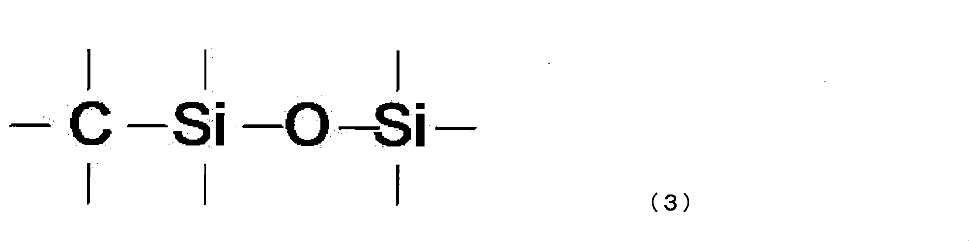
後述のポリシロキサンセグメント(a1)が有するシラノール基および/または加水分解性シリル基と、後述のビニル系重合体セグメント(a2)が有するシラノール基および/または加水分解性シリル基とが脱水縮合反応して、前記一般式(3)で表される結合が生じる。従って前記一般式(3)中、炭素原子は前記ビニル系重合体セグメント(a2)の一部分を構成し、酸素原子のみに結合したケイ素原子は、前記ポリシロキサンセグメント(a1)の一部分を構成するものとする。
複合樹脂(A)の形態は、例えば、前記ポリシロキサンセグメント(a1)が前記重合体セグメント(a2)の側鎖として化学的に結合したグラフト構造を有する複合樹脂や、前記重合体セグメント(a2)と前記ポリシロキサンセグメント(a1)とが化学的に結合したブロック構造を有する複合樹脂等が挙げられる。
複合樹脂(A)の形態は、例えば、前記ポリシロキサンセグメント(a1)が前記重合体セグメント(a2)の側鎖として化学的に結合したグラフト構造を有する複合樹脂や、前記重合体セグメント(a2)と前記ポリシロキサンセグメント(a1)とが化学的に結合したブロック構造を有する複合樹脂等が挙げられる。
(ポリシロキサンセグメント(a1))
本発明におけるポリシロキサンセグメント(a1)は、一般式(1)および/または一般式(2)で表される構造単位と、シラノール基および/または加水分解性シリル基とを有すセグメントである。一般式(1)および/または一般式(2)で表される構造単位中には重合性二重結合を有する基が含まれている。
本発明におけるポリシロキサンセグメント(a1)は、一般式(1)および/または一般式(2)で表される構造単位と、シラノール基および/または加水分解性シリル基とを有すセグメントである。一般式(1)および/または一般式(2)で表される構造単位中には重合性二重結合を有する基が含まれている。
(一般式(1)および/または一般式(2)で表される構造単位)
前記一般式(1)および/または前記一般式(2)で表される構造単位は、重合性二重結合を有する基を必須成分として有している。
具体的には、前記一般式(1)及び(2)におけるR1、R2及びR3は、それぞれ独立して、-R4-CH=CH2、-R4-C(CH3)=CH2、-R4-O-CO-C(CH3)=CH2、及び-R4-O-CO-CH=CH2からなる群から選ばれる1つの重合性二重結合を有する基(但しR4は単結合又は炭素原子数1~6のアルキレン基を表す)、炭素原子数が1~6のアルキル基、炭素原子が3~8のシクロアルキル基、アリール基または炭素原子が7~12のアラルキル基を表し、R1、R2及びR3の少なくとも1つは前記重合性二重結合を有する基である。また前記R4における前記炭素原子数が1~6のアルキレン基としては、例えば、メチレン基、エチレン基、プロピレン基、イソプロピレン基、ブチレン基、イソブチレン基、sec-ブチレン基、tert-ブチレン基、ペンチレン基、イソペンチレン基、ネオペンチレン基、tert-ペンチレン基、1-メチルブチレン基、2-メチルブチレン基、1,2-ジメチルプロピレン基、1-エチルプロピレン基、ヘキシレン基、イソヘシレン基、1-メチルペンチレン基、2-メチルペンチレン基、3-メチルペンチレン基、1,1-ジメチルブチレン基、1,2-ジメチルブチレン基、2,2-ジメチルブチレン基、1-エチルブチレン基、1,1,2-トリメチルプロピレン基、1,2,2-トリメチルプロピレン基、1-エチル-2-メチルプロピレン基、1-エチル-1-メチルプロピレン基等が挙げられる。中でもR4は、原料の入手の容易さから単結合または炭素原子数が2~4のアルキレン基が好ましい。
前記一般式(1)および/または前記一般式(2)で表される構造単位は、重合性二重結合を有する基を必須成分として有している。
具体的には、前記一般式(1)及び(2)におけるR1、R2及びR3は、それぞれ独立して、-R4-CH=CH2、-R4-C(CH3)=CH2、-R4-O-CO-C(CH3)=CH2、及び-R4-O-CO-CH=CH2からなる群から選ばれる1つの重合性二重結合を有する基(但しR4は単結合又は炭素原子数1~6のアルキレン基を表す)、炭素原子数が1~6のアルキル基、炭素原子が3~8のシクロアルキル基、アリール基または炭素原子が7~12のアラルキル基を表し、R1、R2及びR3の少なくとも1つは前記重合性二重結合を有する基である。また前記R4における前記炭素原子数が1~6のアルキレン基としては、例えば、メチレン基、エチレン基、プロピレン基、イソプロピレン基、ブチレン基、イソブチレン基、sec-ブチレン基、tert-ブチレン基、ペンチレン基、イソペンチレン基、ネオペンチレン基、tert-ペンチレン基、1-メチルブチレン基、2-メチルブチレン基、1,2-ジメチルプロピレン基、1-エチルプロピレン基、ヘキシレン基、イソヘシレン基、1-メチルペンチレン基、2-メチルペンチレン基、3-メチルペンチレン基、1,1-ジメチルブチレン基、1,2-ジメチルブチレン基、2,2-ジメチルブチレン基、1-エチルブチレン基、1,1,2-トリメチルプロピレン基、1,2,2-トリメチルプロピレン基、1-エチル-2-メチルプロピレン基、1-エチル-1-メチルプロピレン基等が挙げられる。中でもR4は、原料の入手の容易さから単結合または炭素原子数が2~4のアルキレン基が好ましい。
また、前記炭素原子数が1~6のアルキル基としては、例えば、メチル基、エチル基、プロピル基、イソプロピル基、ブチル基、イソブチル基、sec-ブチル基、tert-ブチル基、ペンチル基、イソペンチル基、ネオペンチル基、tert-ペンチル基、1-メチルブチル基、2-メチルブチル基、1,2-ジメチルプロピル基、1-エチルプロピル基、ヘキシル基、イソヘシル基、1-メチルペンチル基、2-メチルペンチル基、3-メチルペンチル基、1,1-ジメチルブチル基、1,2-ジメチルブチル基、2,2-ジメチルブチル基、1-エチルブチル基、1,1,2-トリメチルプロピル基、1,2,2-トリメチルプロピル基、1-エチル-2-メチルプロピル基、1-エチル-1-メチルプロピル基等が挙げられる。
また、前記炭素原子数が3~8のシクロアルキル基としては、例えば、シクロプロピル基、シクロブチル基、シクロペンチル基、シクロヘキシル基等が挙げられる。また、前記アリール基としては、例えば、フェニル基、ナフチル基、2-メチルフェニル基、3-メチルフェニル基、4-メチルフェニル基、4-ビニルフェニル基、3-イソプロピルフェニル基等が挙げられる。
また、前記炭素原子数が7~12のアラルキル基としては、例えば、ベンジル基、ジフェニルメチル基、ナフチルメチル基等が挙げられる。
また、前記炭素原子数が3~8のシクロアルキル基としては、例えば、シクロプロピル基、シクロブチル基、シクロペンチル基、シクロヘキシル基等が挙げられる。また、前記アリール基としては、例えば、フェニル基、ナフチル基、2-メチルフェニル基、3-メチルフェニル基、4-メチルフェニル基、4-ビニルフェニル基、3-イソプロピルフェニル基等が挙げられる。
また、前記炭素原子数が7~12のアラルキル基としては、例えば、ベンジル基、ジフェニルメチル基、ナフチルメチル基等が挙げられる。
また、R1、R2及びR3の少なくとも1つは前記重合性二重結合を有する基であるとは、具体的には、ポリシロキサンセグメント(a1)が一般式(1)で表される構造単位のみを有する場合にはR1が前記重合性二重結合を有する基であり、ポリシロキサンセグメント(a1)が一般式(2)で表される構造単位のみを有する場合にはR2及び/又はR3が前記重合性二重結合を有する基であり、ポリシロキサンセグメント(a1)が一般式(1)と一般式(2)で表される構造単位の両方を有する場合には、R1、R2及びR3の少なくとも1つが重合性二重結合を有する基であることを示す。
本発明においては、前記重合性二重結合は、ポリシロキサンセグメント(a1)中に2つ以上存在することが好ましく、3~200個存在することがより好ましく、3~50個存在することが更に好ましく、耐久性に優れた塗膜を得ることができる。具体的には、前記ポリシロキサンセグメント(a1)中の重合性二重結合の含有率が3~35重量%であれば、所望の耐候性および密着性を得ることができる。尚、ここでいう重合性二重結合とは、ビニル基、ビニリデン基もしくはビニレン基のうち、フリーラジカルによる生長反応を行うことができる基の総称である。また、重合性二重結合の含有率とは、当該ビニル基、ビニリデン基もしくはビニレン基のポリシロキサンセグメント中における重量%を示すものである。
重合性二重結合を有する基としては、当該ビニル基、ビニリデン基、ビニレン基を含有してなる公知の全ての官能基を使用することができるが、中でも-R4-C(CH3)=CH2や-R4-O-CO-C(CH3)=CH2で表される(メタ)アクリロイル基は、紫外線硬化の際の反応性に富むことや、後述のビニル系重合体セグメント(a2)との相溶性が良好であり、透明性に優れる硬化塗膜が得られることから好ましい。
重合性二重結合を有する基としては、当該ビニル基、ビニリデン基、ビニレン基を含有してなる公知の全ての官能基を使用することができるが、中でも-R4-C(CH3)=CH2や-R4-O-CO-C(CH3)=CH2で表される(メタ)アクリロイル基は、紫外線硬化の際の反応性に富むことや、後述のビニル系重合体セグメント(a2)との相溶性が良好であり、透明性に優れる硬化塗膜が得られることから好ましい。
前記一般式(1)および/または前記一般式(2)で表される構造単位は、ケイ素の結合手のうち2または3つが架橋に関与した、三次元網目状のポリシロキサン構造単位である。三次元網目構造を形成しながらも密な網目構造を形成しないので、製造あるいはプライマー形成時にゲル化等を生じることもなく保存安定性も良好となる。
(シラノール基および/または加水分解性シリル基)
本発明においてシラノール基とは、珪素原子に直接結合した水酸基を有する珪素含有基である。該シラノール基は具体的には、前記一般式(1)および/または前記一般式(2)で表される構造単位の、結合手を有する酸素原子が水素原子と結合して生じたシラノール基であることが好ましい。
本発明においてシラノール基とは、珪素原子に直接結合した水酸基を有する珪素含有基である。該シラノール基は具体的には、前記一般式(1)および/または前記一般式(2)で表される構造単位の、結合手を有する酸素原子が水素原子と結合して生じたシラノール基であることが好ましい。
また本発明において加水分解性シリル基とは、珪素原子に直接結合した加水分解性基を有する珪素含有基であり、具体的には、例えば、一般式(4)で表される基が挙げられる。
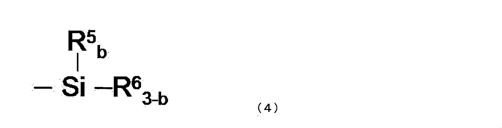
(一般式(4)中、R5はアルキル基、アリール基又はアラルキル基等の1価の有機基を、R6はハロゲン原子、アルコキシ基、アシロキシ基、フェノキシ基、アリールオキシ基、メルカプト基、アミノ基、アミド基、アミノオキシ基、イミノオキシ基及びアルケニルオキシ基からなる群から選ばれる加水分解性基である。またbは0~2の整数である。)
前記R5において、アルキル基としては、例えば、メチル基、エチル基、プロピル基、イソプロピル基、ブチル基、イソブチル基、sec-ブチル基、tert-ブチル基、ペンチル基、イソペンチル基、ネオペンチル基、tert-ペンチル基、1-メチルブチル基、2-メチルブチル基、1,2-ジメチルプロピル基、1-エチルプロピル基、ヘキシル基、イソヘシル基、1-メチルペンチル基、2-メチルペンチル基、3-メチルペンチル基、1,1-ジメチルブチル基、1,2-ジメチルブチル基、2,2-ジメチルブチル基、1-エチルブチル基、1,1,2-トリメチルプロピル基、1,2,2-トリメチルプロピル基、1-エチル-2-メチルプロピル基、1-エチル-1-メチルプロピル基等が挙げられる。
またアリール基としては、例えば、フェニル基、ナフチル基、2-メチルフェニル基、3-メチルフェニル基、4-メチルフェニル基、4-ビニルフェニル基、3-イソプロピルフェニル基等が挙げられる。
またアラルキル基としては、例えば、ベンジル基、ジフェニルメチル基、ナフチルメチル基等が挙げられる。
またアリール基としては、例えば、フェニル基、ナフチル基、2-メチルフェニル基、3-メチルフェニル基、4-メチルフェニル基、4-ビニルフェニル基、3-イソプロピルフェニル基等が挙げられる。
またアラルキル基としては、例えば、ベンジル基、ジフェニルメチル基、ナフチルメチル基等が挙げられる。
前記R6において、ハロゲン原子としては、例えば、フッ素原子、塩素原子、臭素原子、ヨウ素原子等が挙げられる。
アルコキシ基としては、例えば、メトキシ基、エトキシ基、プロポキシ基、イソプロポキシ基、ブトキシ基、第二ブトキシ基、第三ブトキシ基等が挙げられる。
またアシロキシ基としては、例えば、ホルミルオキシ、アセトキシ、プロパノイルオキシ、ブタノイルオキシ、ピバロイルオキシ、ペンタノイルオキシ、フェニルアセトキシ、アセトアセトキシ、ベンゾイルオキシ、ナフトイルオキシ等が挙げられる。
またアリールオキシ基としては、例えば、フェニルオキシ、ナフチルオキシ等が挙げられる。
アルケニルオキシ基としては、例えば、ビニルオキシ基、アリルオキシ基、1-プロペニルオキシ基、イソプロペニルオキシ基、2-ブテニルオキシ基、3-ブテニルオキシ基、2-ペテニルオキシ基、3-メチル-3-ブテニルオキシ基、2-ヘキセニルオキシ基等が挙げられる。
アルコキシ基としては、例えば、メトキシ基、エトキシ基、プロポキシ基、イソプロポキシ基、ブトキシ基、第二ブトキシ基、第三ブトキシ基等が挙げられる。
またアシロキシ基としては、例えば、ホルミルオキシ、アセトキシ、プロパノイルオキシ、ブタノイルオキシ、ピバロイルオキシ、ペンタノイルオキシ、フェニルアセトキシ、アセトアセトキシ、ベンゾイルオキシ、ナフトイルオキシ等が挙げられる。
またアリールオキシ基としては、例えば、フェニルオキシ、ナフチルオキシ等が挙げられる。
アルケニルオキシ基としては、例えば、ビニルオキシ基、アリルオキシ基、1-プロペニルオキシ基、イソプロペニルオキシ基、2-ブテニルオキシ基、3-ブテニルオキシ基、2-ペテニルオキシ基、3-メチル-3-ブテニルオキシ基、2-ヘキセニルオキシ基等が挙げられる。
前記R6で表される加水分解性基が加水分解されることにより、一般式(4)で表される加水分解性シリル基はシラノール基となる。加水分解性に優れることから、中でも、メトキシ基およびエトキシ基が好ましい。
また前記加水分解性シリル基は具体的には、前記一般式(1)および/または前記一般式(2)で表される構造単位の、結合手を有する酸素原子が前記加水分解性基と結合もしくは置換されている加水分解性シリル基であることが好ましい。
また前記加水分解性シリル基は具体的には、前記一般式(1)および/または前記一般式(2)で表される構造単位の、結合手を有する酸素原子が前記加水分解性基と結合もしくは置換されている加水分解性シリル基であることが好ましい。
前記シラノール基や前記加水分解性シリル基は、前記重合性二重結合を有する基の硬化反応による塗膜形成の際に、該硬化反応と平行して、シラノール基中の水酸基や加水分解性シリル基中の前記加水分解性基の間で加水分解縮合反応が進行するので、得られる塗膜のポリシロキサン構造の架橋密度が高まり、耐溶剤性などに優れた塗膜を形成することができる。
また、前記シラノール基や前記加水分解性シリル基を含むポリシロキサンセグメント(a1)と後述のビニル系重合体セグメント(a2)とを、前記一般式(3)で表される結合を介して結合させる際に使用する。
また、前記シラノール基や前記加水分解性シリル基を含むポリシロキサンセグメント(a1)と後述のビニル系重合体セグメント(a2)とを、前記一般式(3)で表される結合を介して結合させる際に使用する。
ポリシロキサンセグメント(a1)は、前記一般式(1)および/または前記一般式(2)で表される構造単位と、シラノール基および/または加水分解性シリル基とを有する以外は特に限定はなく、他の基を含んでいてもよい。例えば、
前記一般式(1)におけるR1が前記重合性二重結合を有する基である構造単位と、前記一般式(1)におけるR1がメチル等のアルキル基である構造単位とが共存したポリシロキサンセグメント(a1)であってもよいし、
前記一般式(1)におけるR1が前記重合性二重結合を有する基である構造単位と、前記一般式(1)におけるR1がメチル基等のアルキル基である構造単位と、前記一般式(2)におけるR2及びR3がメチル基等のアルキル基である構造単位とが共存したポリシロキサンセグメント(a1)であってもよいし、
前記一般式(1)におけるR1が前記重合性二重結合を有する基である構造単位と、前記一般式(2)におけるR2及びR3がメチル基等のアルキル基である構造単位とが共存したポリシロキサンセグメント(a1)であってもよいし、特に限定はない。
具体的には、ポリシロキサンセグメント(a1)としては、例えば以下の構造を有するもの等が挙げられる。
前記一般式(1)におけるR1が前記重合性二重結合を有する基である構造単位と、前記一般式(1)におけるR1がメチル等のアルキル基である構造単位とが共存したポリシロキサンセグメント(a1)であってもよいし、
前記一般式(1)におけるR1が前記重合性二重結合を有する基である構造単位と、前記一般式(1)におけるR1がメチル基等のアルキル基である構造単位と、前記一般式(2)におけるR2及びR3がメチル基等のアルキル基である構造単位とが共存したポリシロキサンセグメント(a1)であってもよいし、
前記一般式(1)におけるR1が前記重合性二重結合を有する基である構造単位と、前記一般式(2)におけるR2及びR3がメチル基等のアルキル基である構造単位とが共存したポリシロキサンセグメント(a1)であってもよいし、特に限定はない。
具体的には、ポリシロキサンセグメント(a1)としては、例えば以下の構造を有するもの等が挙げられる。
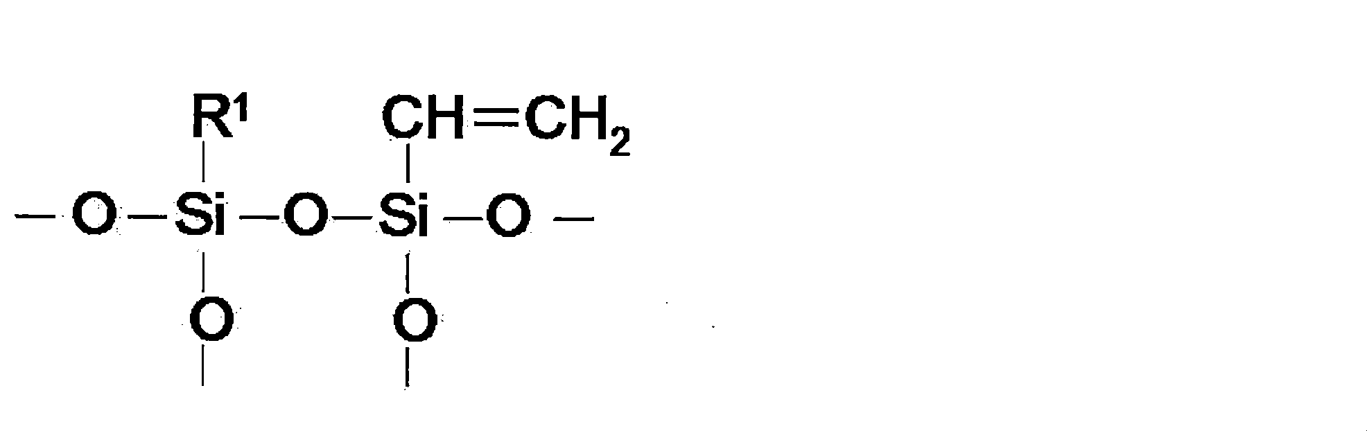
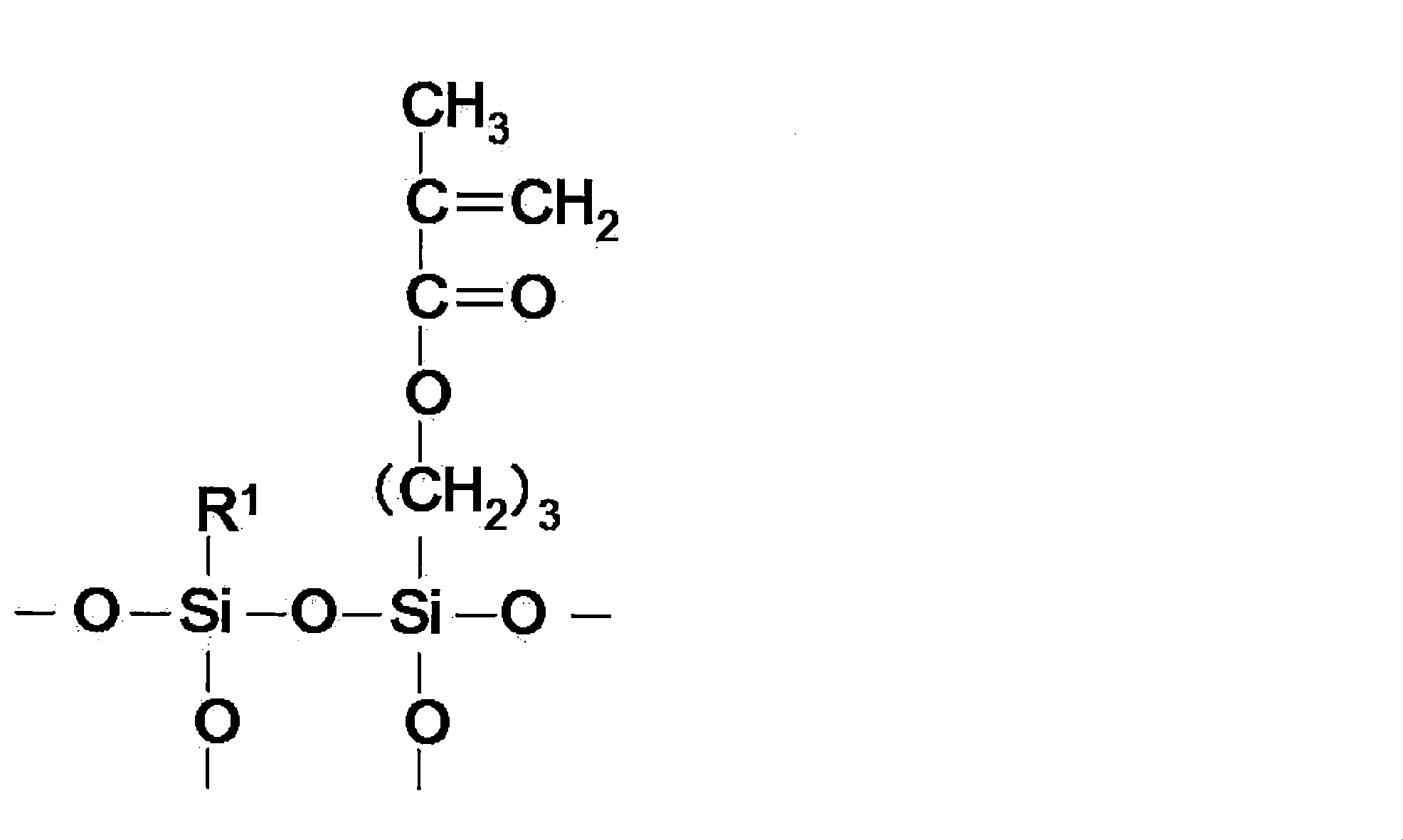

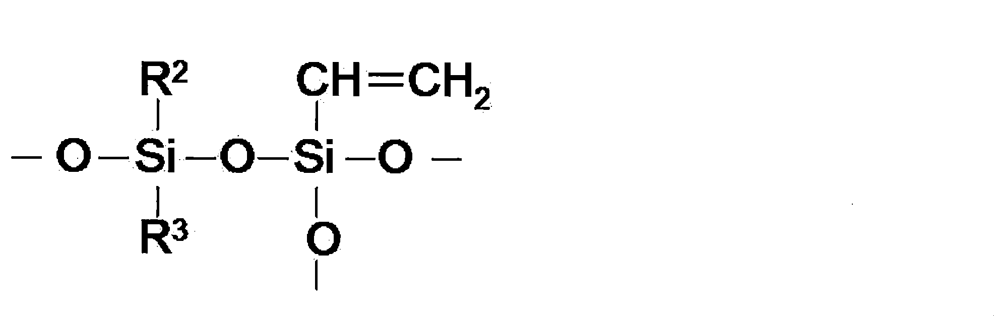
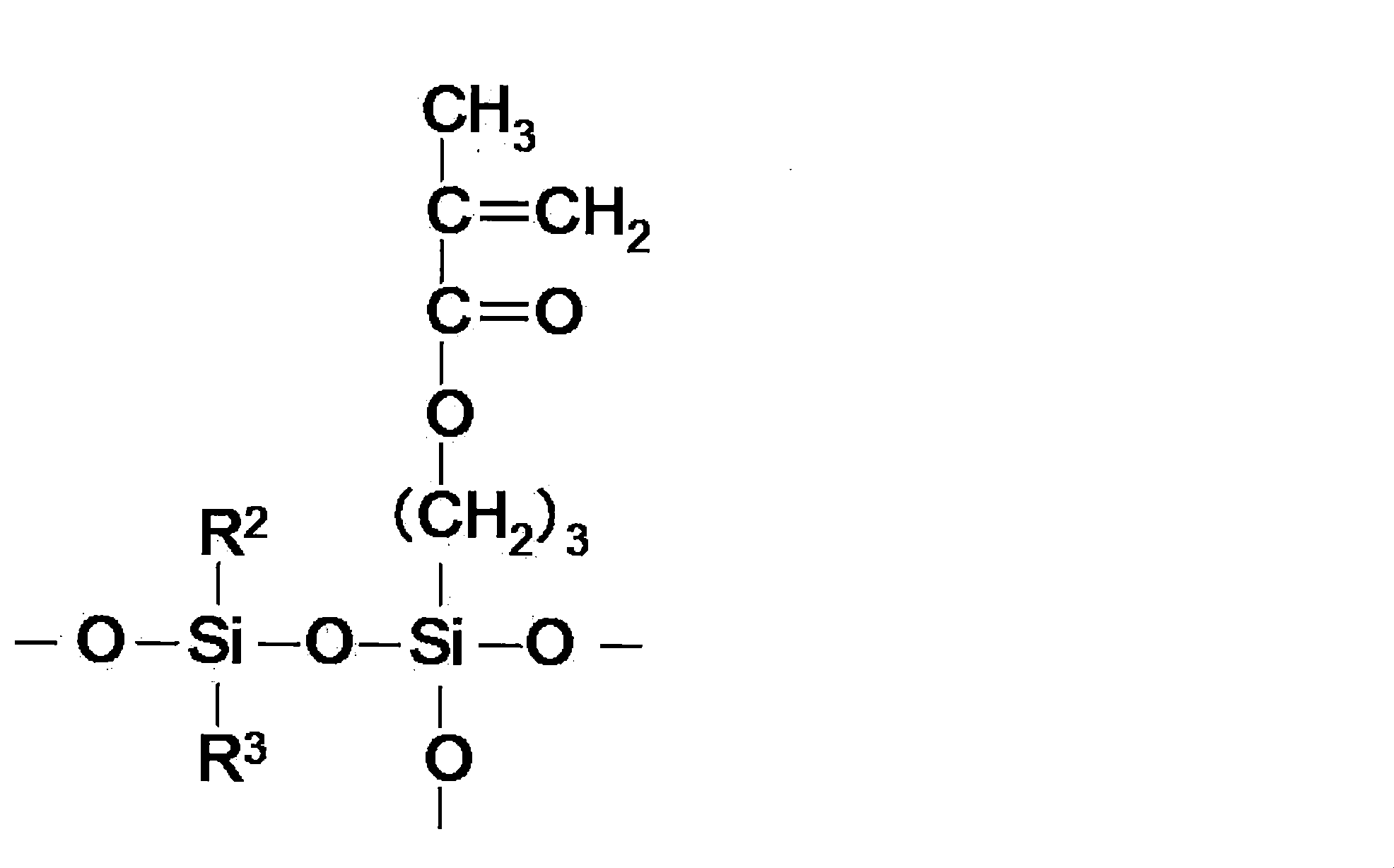

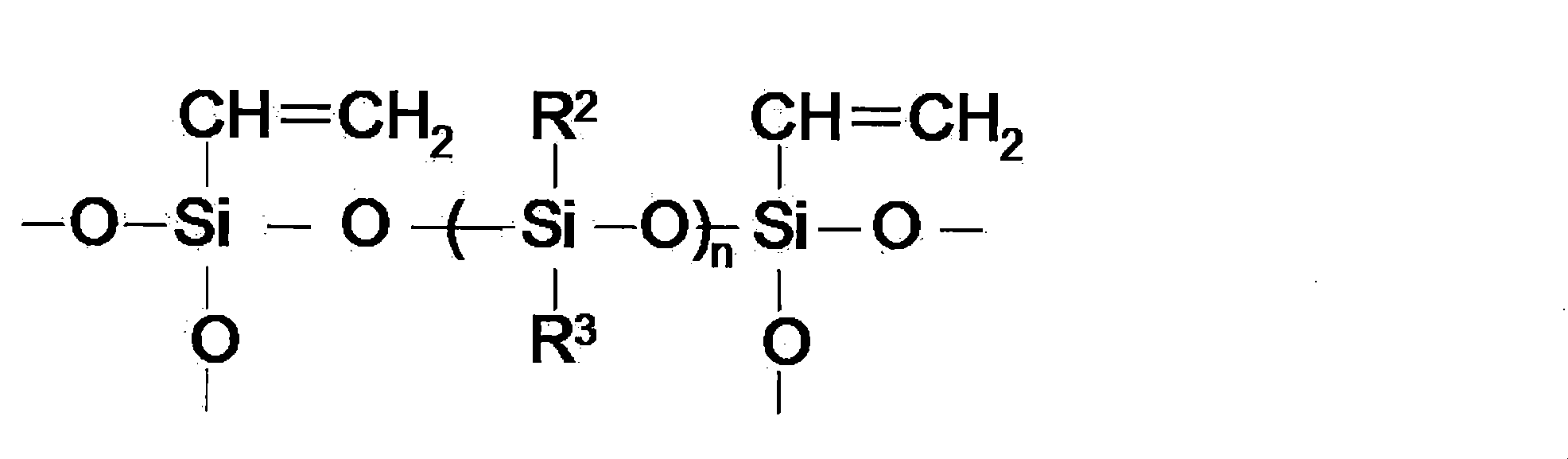

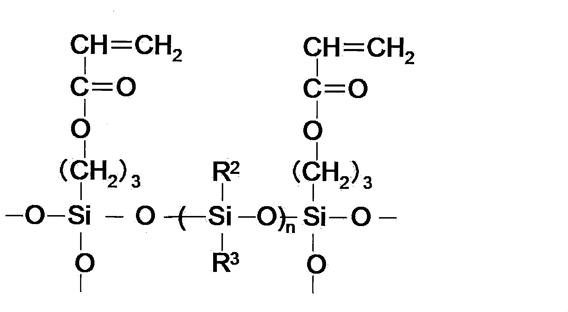
本発明においては、前記ポリシロキサンセグメント(a1)を、樹脂層(I)を構成する前記活性エネルギー線硬化性樹脂組成物の全固形分量に対して10~65重量%含むことが好ましく、プラスチック基材および無機酸化物蒸着膜層(II)との密着性および耐候性を両立させることが可能となる。
(ビニル系重合体セグメント(a2))
本発明におけるビニル系重合体セグメント(a2)は、アクリル系重合体、フルオロオレフィン系重合体、ビニルエステル系重合体、芳香族系ビニル系重合体、ポリオレフィン系重合体等のビニル重合体セグメントであり、中でもアクリル系重合体セグメントが、得られる塗膜の透明性や光沢に優れることから好ましい。
本発明におけるビニル系重合体セグメント(a2)は、アクリル系重合体、フルオロオレフィン系重合体、ビニルエステル系重合体、芳香族系ビニル系重合体、ポリオレフィン系重合体等のビニル重合体セグメントであり、中でもアクリル系重合体セグメントが、得られる塗膜の透明性や光沢に優れることから好ましい。
アクリル系重合性セグメントは、汎用の(メタ)アクリルモノマーを重合または共重合させて得られる。(メタ)アクリルモノマーとしては特に限定はなく、またビニルモノマーも共重合可能である。例えば、メチル(メタ)アクリレート、エチル(メタ)アクリレート、n-プロピル(メタ)アクリレート、n-ブチル(メタ)アクリレート、イソブチル(メタ)アクリレート、tert-ブチル(メタ)アクリレート、2-エチルヘキシル(メタ)アクリレート、ラウリル(メタ)アクリレート等の炭素原子数が1~22のアルキル基を有するアルキル(メタ)アクリレート類;ベンジル(メタ)アクリレート、2-フェニルエチル(メタ)アクリレート等のアラルキル(メタ)アクリレート類;シクロヘキシル(メタ)アクリレート、イソボルニル(メタ)アクリレート等のシクロアルキル(メタ)アクリレート類;2-メトキシエチル(メタ)アクリレート、4-メトキシブチル(メタ)アクリレート等のω-アルコキシアルキル(メタ)アクリレート類;スチレン、p-tert-ブチルスチレン、α-メチルスチレン、ビニルトルエン等の芳香族ビニル系モノマー類;酢酸ビニル、プロピオン酸ビニル、ピバリン酸ビニル、安息香酸ビニル等のカルボン酸ビニルエステル類;クロトン酸メチル、クロトン酸エチル等のクロトン酸のアルキルエステル類;ジメチルマレート、ジ-n-ブチルマレート、ジメチルフマレート、ジメチルイタコネート等の不飽和二塩基酸のジアルキルエステル類;エチレン、プロピレン等のα-オレフィン類;フッ化ビニリデン、テトラフルオロエチレン、ヘキサフルオロプロピレン、クロロトリフルオロエチレン等のフルオロオレフィン類;エチルビニルエーテル、n-ブチルビニルエーテル等のアルキルビニルエーテル類;シクロペンチルビニルエーテル、シクロヘキシルビニルエーテル等のシクロアルキルビニルエーテル類;N,N-ジメチル(メタ)アクリルアミド、N-(メタ)アクリロイルモルホリン、N-(メタ)アクリロイルピロリジン、N-ビニルピロリドン等の3級アミド基含有モノマー類等が挙げられる。
また、本発明におけるビニル系重合体セグメント(a2)は、プラスチック基材との密着性を向上させる観点から環状炭化水素基を有する(メタ)アクリル繰り返し単位がより好ましい。前記環状炭化水素基を有する(メタ)アクリル繰り返し単位として好ましくはシクロヘキシル(メタ)アクリレート、シクロペンタニル(メタ)アクリレート、アダマンチル(メタ)アクリレート、トリシクロデカニル(メタ)アクリレート、テトラシクロドデカニル(メタ)アクリレート、ジシクロペンタニル(メタ)アクリレート、イソボルニルアクリレート、などの環状炭化水素基を有する(メタ)アクリレートが挙げられる。これらは単独で又は2種以上を組み合わせても用いることができる。
前記モノマーを共重合させる際の重合方法、溶剤、あるいは重合開始剤にも特に限定はなく、公知の方法によりビニル系重合体セグメント(a2)を得ることができる。例えば、塊状ラジカル重合法、溶液ラジカル重合法、非水分散ラジカル重合法等の種々の重合法により、2,2’-アゾビス(イソブチロニトリル)、2,2’-アゾビス(2,4-ジメチルバレロニトリル)、2,2’-アゾビス(2-メチルブチロニトリル)、tert-ブチルパーオキシピバレート、tert-ブチルパーオキシベンゾエート、tert-ブチルパーオキシ-2-エチルヘキサノエート、ジ-tert-ブチルパーオキサイド、クメンハイドロパーオキサイド、ジイソプロピルパーオキシカーボネート等の重合開始剤を使用してビニル系重合体セグメント(a2)を得ることができる。
前記ビニル系重合体セグメント(a2)の数平均分子量としては、数平均分子量(以下Mnと略す)に換算して500~200,000の範囲であることが好ましく、前記複合樹脂(A)を製造する際の増粘やゲル化を防止でき、且つ耐久性に優れる。Mnは中でも700~100,000の範囲がより好ましく、1,000~50,000の範囲が後記する基材への塗装適性および密着性の理由からなお好ましい。
また前記ビニル系重合体セグメント(a2)は、前記ポリシロキサンセグメント(a1)と一般式(3)で表される結合により結合された複合樹脂(A)とするために、ビニル系重合体セグメント(a2)中の炭素結合に直接結合したシラノール基および/または加水分解性シリル基を有する。これらのシラノール基および/または加水分解性シリル基は、後述の複合樹脂(A)の製造において一般式(3)で表される結合となってしまうために、最終生成物である複合樹脂(A)中のビニル系重合体セグメント(a2)には殆ど存在しない。しかしながらビニル系重合体セグメント(a2)にシラノール基および/または加水分解性シリル基が残存していても何ら問題はなく、前記重合性二重結合を有する基の硬化反応による塗膜形成の際に、該硬化反応と平行して、シラノール基中の水酸基や加水分解性シリル基中の前記加水分解性基の間で加水分解縮合反応が進行するので、得られる塗膜のポリシロキサン構造の架橋密度が高まり、耐久性に優れた塗膜を形成することが
できる。
できる。
炭素結合に直接結合したシラノール基および/または加水分解性シリル基を有するビニル系重合体セグメント(a2)は、具体的には、前記汎用モノマー、及び、炭素結合に直接結合したシラノール基および/または加水分解性シリル基を含有するビニル系モノマーとを共重合させて得る。
炭素結合に直接結合したシラノール基および/または加水分解性シリル基を含有するビニル系モノマーとしては、例えば、ビニルトリメトキシシラン、ビニルトリエトキシシラン、ビニルメチルジメトキシシラン、ビニルトリ(2-メトキシエトキシ)シラン、ビニルトリアセトキシシラン、ビニルトリクロロシラン、2-トリメトキシシリルエチルビニルエーテル、3-(メタ)アクリロイルオキシプロピルトリメトキシシラン、3-(メタ)アクリロイルオキシプロピルトリエトキシシラン、3-(メタ)アクリロイルオキシプロピルメチルジメトキシシラン、3-(メタ)アクリロイルオキシプロピルトリクロロシラン等が挙げられる。中でも、加水分解反応を容易に進行でき、また反応後の副生成物を容易に除去することができることからビニルトリメトキシシラン、3-(メタ)アクリロイルオキシプロピルトリメトキシシランが好ましい。
炭素結合に直接結合したシラノール基および/または加水分解性シリル基を含有するビニル系モノマーとしては、例えば、ビニルトリメトキシシラン、ビニルトリエトキシシラン、ビニルメチルジメトキシシラン、ビニルトリ(2-メトキシエトキシ)シラン、ビニルトリアセトキシシラン、ビニルトリクロロシラン、2-トリメトキシシリルエチルビニルエーテル、3-(メタ)アクリロイルオキシプロピルトリメトキシシラン、3-(メタ)アクリロイルオキシプロピルトリエトキシシラン、3-(メタ)アクリロイルオキシプロピルメチルジメトキシシラン、3-(メタ)アクリロイルオキシプロピルトリクロロシラン等が挙げられる。中でも、加水分解反応を容易に進行でき、また反応後の副生成物を容易に除去することができることからビニルトリメトキシシラン、3-(メタ)アクリロイルオキシプロピルトリメトキシシランが好ましい。
また、後述のポリイソシアネート(B)を含有する際には、前記ビニル系重合体セグメント(a2)はアルコール性水酸基を有することが好ましい。アルコール性水酸基を有するビニル系重合体セグメント(a2)は、アルコール水酸基を有する(メタ)アクリルモノマーを共重合させて得ることができる。アルコール水酸基を有する(メタ)アクリルモノマーとしては、具体的には、2-ヒドロキシエチル(メタ)アクリレート、2-ヒドロキシプロピル(メタ)アクリレート、3-ヒドロキシプロピル(メタ)アクリレート、2-ヒドロキシブチル(メタ)アクリレート、3-ヒドロキシブチル(メタ)アクリレート、4-ヒドロキシブチル(メタ)アクリレート、3-クロロ-2-ヒドロキシプロピル(メタ)アクリレート、ジ-2-ヒドロキシエチルフマレート、モノ-2-ヒドロキシエチルモノブチルフマレート、ポリエチレングルコールモノ(メタ)アクリレート、ポリプロピレングリコールモノ(メタ)アクリレート、「プラクセルFMもしくはプラクセルFA」〔ダイセル化学(株)製のカプロラクトン付加モノマー〕等の各種α、β-エチレン性不飽和カルボン酸のヒドロキシアルキルエステル類、またはこれらとε-カプロラクトンとの付加物、等が挙げられる。
中でも2-ヒドロキシエチル(メタ)アクリレートが、反応が容易であり好ましい。
中でも2-ヒドロキシエチル(メタ)アクリレートが、反応が容易であり好ましい。
前記アルコール性水酸基量は、後述のポリイソシアネート(B)の添加量から算出して適宜決定するのが好ましい。
また、後述の通り本発明においてはアルコール性水酸基を有する活性エネルギー線硬化性モノマーを併用してもより好ましい。従ってアルコール性水酸基を有するビニル系重合体セグメント(a2)中のアルコール性水酸基量は、併用するアルコール性水酸基を有する活性エネルギー線硬化性モノマーの量まで加味して決定することができる。実質的にはビニル系重合体セグメント(a2)の水酸基価に換算して30~300の範囲となるように含有することが好ましい。
また、後述の通り本発明においてはアルコール性水酸基を有する活性エネルギー線硬化性モノマーを併用してもより好ましい。従ってアルコール性水酸基を有するビニル系重合体セグメント(a2)中のアルコール性水酸基量は、併用するアルコール性水酸基を有する活性エネルギー線硬化性モノマーの量まで加味して決定することができる。実質的にはビニル系重合体セグメント(a2)の水酸基価に換算して30~300の範囲となるように含有することが好ましい。
(活性エネルギー線硬化性樹脂組成物の複合樹脂(A)の製造方法)
本発明で用いる複合樹脂(A)は、具体的には下記(方法1)~(方法3)に示す方法で製造する。
本発明で用いる複合樹脂(A)は、具体的には下記(方法1)~(方法3)に示す方法で製造する。
(方法1)前記汎用の(メタ)アクリルモノマー等、及び、前記炭素結合に直接結合したシラノール基および/または加水分解性シリル基を含有するビニル系モノマーとを共重合させて炭素結合に直接結合したシラノール基および/または加水分解性シリル基を含有するビニル系重合体セグメント(a2)を得る。これに、シラノール基および/または加水分解性シリル基並びに重合性二重結合を併有するシラン化合物、必要に応じて汎用のシラン化合物とを混合し、加水分解縮合反応させる。
該方法においては、シラノール基および/または加水分解性シリル基並びに重合性二重結合を併有するシラン化合物のシラノール基あるいは加水分解性シリル基と、炭素結合に直接結合したシラノール基および/または加水分解性シリル基を含有するビニル系重合体セグメント(a2)が有するシラノール基および/または加水分解性シリル基とが加水分解縮合反応し、前記ポリシロキサンセグメント(a1)が形成されると共に、前記ポリシロキサンセグメント(a1)と、ビニル系重合体セグメント(a2)とが前記一般式(3)で表される結合により複合化された複合樹脂(A)が得られる。
該方法においては、シラノール基および/または加水分解性シリル基並びに重合性二重結合を併有するシラン化合物のシラノール基あるいは加水分解性シリル基と、炭素結合に直接結合したシラノール基および/または加水分解性シリル基を含有するビニル系重合体セグメント(a2)が有するシラノール基および/または加水分解性シリル基とが加水分解縮合反応し、前記ポリシロキサンセグメント(a1)が形成されると共に、前記ポリシロキサンセグメント(a1)と、ビニル系重合体セグメント(a2)とが前記一般式(3)で表される結合により複合化された複合樹脂(A)が得られる。
(方法2)方法1と同様にして、炭素結合に直接結合したシラノール基および/または加水分解性シリル基を含有するビニル系重合体セグメント(a2)を得る。
一方、シラノール基および/または加水分解性シリル基並びに重合性二重結合を併有するシラン化合物、必要に応じて汎用のシラン化合物を加水分解縮合反応させ、ポリシロキサンセグメント(a1)を得る。そして、ビニル系重合体セグメント(a2)が有するシラノール基および/または加水分解性シリル基と、とポリシロキサンセグメント(a1)とが有するシラノール基および/または加水分解性シリル基とを加水分解縮合反応をさせる。
一方、シラノール基および/または加水分解性シリル基並びに重合性二重結合を併有するシラン化合物、必要に応じて汎用のシラン化合物を加水分解縮合反応させ、ポリシロキサンセグメント(a1)を得る。そして、ビニル系重合体セグメント(a2)が有するシラノール基および/または加水分解性シリル基と、とポリシロキサンセグメント(a1)とが有するシラノール基および/または加水分解性シリル基とを加水分解縮合反応をさせる。
(方法3)方法1と同様に、炭素結合に直接結合したシラノール基および/または加水分解性シリル基を含有するビニル系重合体セグメント(a2)を得る。一方、方法2と同様にして、ポリシロキサンセグメント(a1)を得る。更に、重合性二重結合を併有するシラン化合物を含有するシラン化合物と、必要に応じて汎用のシラン化合物とを混合し、加水分解縮合反応させる。
前記(方法1)~(方法3)で使用する、シラノール基および/または加水分解性シリル基並びに重合性二重結合を併有するシラン化合物としては、具体的には、例えば、ビニルトリメトキシシラン、ビニルトリエトキシシラン、ビニルメチルジメトキシシラン、ビニルトリ(2-メトキシエトキシ)シラン、ビニルトリアセトキシシラン、ビニルトリクロロシラン、2-トリメトキシシリルエチルビニルエーテル、3-(メタ)アクリロイルオキシプロピルトリメトキシシラン、3-(メタ)アクリロイルオキシプロピルトリエトキシシラン、3-(メタ)アクリロイルオキシプロピルメチルジメトキシシラン、3-(メタ)アクリロイルオキシプロピルトリクロロシラン等が挙げられる。中でも、加水分解反応を容易に進行でき、また反応後の副生成物を容易に除去することができることからビニルトリメトキシシラン、3-(メタ)アクリロイルオキシプロピルトリメトキシシランが好ましい。
また、前記(方法1)~(方法3)で使用する、汎用のシラン化合物としては、例えば、メチルトリメトキシシラン、メチルトリエトキシシラン、メチルトリ-n-ブトキシシラン、エチルトリメトキシシラン、n-プロピルトリメトキシシラン、iso-ブチルトリメトキシシラン、シクロヘキシルトリメトキシシラン、フェニルトリメトキシシラン、フェニルトリエトキシシラン等の各種のオルガノトリアルコキシシラン類;ジメチルジメトキシシラン、ジメチルジエトキシシラン、ジメチルジ-n-ブトキシシラン、ジエチルジメトキシシラン、ジフェニルジメトキシシラン、メチルシクロヘキシルジメトキシシランもしくはメチルフェニルジメトキシシラン等の、各種のジオルガノジアルコキシシラン類;メチルトリクロロシラン、エチルトリクロロシラン、フェニルトリクロロシラン、ビニルトリクロロシラン、ジメチルジクロロシラン、ジエチルジクロロシランもしくはジフェニルジクロロシラン等のクロロシラン類が挙げられる。中でも、加水分解反応が容易に進行し、また反応後の副生成物を容易に除去することが可能なオルガノトリアルコキシシランやジオルガノジアルコキシシランが好ましい。
また、テトラメトキシシラン、テトラエトキシシランもしくはテトラn-プロポキシシランなどの4官能アルコキシシラン化合物や該4官能アルコキシシラン化合物の部分加水分解縮合物を、本発明の効果を損なわない範囲で併用することもできる。前記4官能アルコキシシラン化合物又はその部分加水分解縮合物を併用する場合には、前記ポリシロキサンセグメント(a1)を構成する全珪素原子に対して、該4官能アルコキシシラン化合物の有する珪素原子が、20モル%を超えない範囲となるように併用することが好ましい。
また、前記シラン化合物には、ホウ素、チタン、ジルコニウムあるいはアルミニウムなどの珪素原子以外の金属アルコキシド化合物を、本発明の効果を損なわない範囲で併用することもできる。例えば、ポリシロキサンセグメント(a1)を構成する全珪素原子に対して、上述の金属アルコキシド化合物の有する金属原子が、25モル%を超えない範囲で、併用することが好ましい。
前記(方法1)~(方法3)における加水分解縮合反応は、前記加水分解性基の一部が水などの影響で加水分解され水酸基を形成し、次いで該水酸基同士、あるいは該水酸基と加水分解性基との間で進行する進行する縮合反応をいう。該加水分解縮合反応は、公知の方法で反応を進行させることができるが、前記製造工程で水と触媒とを供給することで反応を進行させる方法が簡便で好ましい。
使用する触媒としては、例えば、塩酸、硫酸、燐酸等の無機酸類;p-トルエンスルホン酸、燐酸モノイソプロピル、酢酸等の有機酸類;水酸化ナトリウム又は水酸化カリウム等の無機塩基類;テトライソプロピルチタネート、テトラブチルチタネート等のチタン酸エステル類;1,8-ジアザビシクロ[5.4.0]ウンデセン-7(DBU)、1,5-ジアザビシクロ[4.3.0]ノネン-5(DBN)、1,4-ジアザビシクロ[2.2.2]オクタン(DABCO)、トリ-n-ブチルアミン、ジメチルベンジルアミン、モノエタノールアミン、イミダゾール、1-メチルイミダゾール等の各種の塩基性窒素原子を含有する化合物類;テトラメチルアンモニウム塩、テトラブチルアンモニウム塩、ジラウリルジメチルアンモニウム塩等の各種の4級アンモニウム塩類であって、対アニオンとして、クロライド、ブロマイド、カルボキシレートもしくはハイドロオキサイドなどを有する4級アンモニウム塩類;ジブチル錫ジアセテート、ジブチル錫ジオクトエート、ジブチル錫ジラウレート、ジブチル錫ジアセチルアセトナート、オクチル酸錫又はステアリン酸錫など錫カルボン酸塩等が挙げられる。触媒は単独で使用しても良いし、2種以上併用しても良い。
前記触媒の添加量に特に限定はないが、一般的には前記シラノール基または加水分解性シリル基を有する各々の化合物全量に対して、0.0001~10重量%の範囲で使用することが好ましく、0.0005~3重量%の範囲で使用することがより好ましく、0.001~1重量%の範囲で使用することが特に好ましい。
また、供給する水の量は、前記シラノール基または加水分解性シリル基を有する各々の化合物が有するシラノール基または加水分解性シリル基1モルに対して0.05モル以上が好ましく、0.1モル以上がより好ましく、特に好ましくは、0.5モル以上である。これらの触媒及び水は、一括供給でも逐次供給であってもよく、触媒と水とを予め混合したものを供給しても良い。
前記(方法1)~(方法3)における加水分解縮合反応を行う際の反応温度は、0℃~150℃の範囲が適切であり、好ましくは、20℃~100℃の範囲内である。また、反応の圧力としては、常圧、加圧下又は減圧下の、いずれの条件においても行うことができる。また、前記加水分解縮合反応において生成しうる副生成物であるアルコールや水は、必要に応じ蒸留などの方法により除去してもよい。
前記(方法1)~(方法3)における各々の化合物の仕込み比率は、所望とする本発明で使用する複合樹脂(A)の構造により適宜選択される。中でも、得られる塗膜の耐久性が優れることから、ポリシロキサンゼグメント(a1)の含有率が30~95重量%となるよう複合樹脂(A)を得るのが好ましく、30~75重量%が更に好ましい。
前記(方法1)~(方法3)において、ポリシロキサンセグメントとビニル系重合体セグメントをブロック状に複合化する具体的な方法としては、ポリマー鎖の片末端あるいは両末端のみに前記したシラノール基および/または加水分解性シリル基を有するような構造のビニル系重合体セグメントを中間体として使用し、例えば、(方法1)であれば、当該ビニル系重合体セグメントに、シラノール基および/または加水分解性シリル基並びに重合性二重結合を併有するシラン化合物、必要に応じて汎用のシラン化合物とを混合し、加水分解縮合反応させる方法が挙げられる。
一方、前記(方法1)~(方法3)において、ビニル系重合体セグメントに対してポリシロキサンセグメントをグラフト状に複合化させる具体的な方法としては、ビニル系重合体セグメントの主鎖に対し、前記したシラノール基および/または加水分解性シリル基をランダムに分布させた構造を有するビニル系重合体セグメントを中間体として使用し、例えば、(方法2)であれば、当該ビニル系重合体セグメントが有するシラノール基および/または加水分解性シリル基と、前記したポリシロキサンセグメントが有するシラノール基および/または加水分解性シリル基とを加水分解縮合反応をさせる方法を挙げることができる。
このようにして調製された下地硬化層は続くプラズマ処理(大気圧、真空)、フレーム処理、コロナ処理、UV(150~400nm)(オゾン)処理、化学薬品処理等の表面処理で層中の有機成分の一部が分解、消失し、表面に向かって傾斜的に無機成分の割合が増加する事になりPE-CVD法による酸化珪素層との密着性を確保するために極めて良好な表面を実現できる。
また更に、本発明の優れた耐環境性もしくは沸水性能を得る上で、下地硬化層の表面は水接触角35°以下であり、DFM法で5μm四方の観察条件で測定した場合の表面粗さ(Ra)が0.7~10.0nmの範囲にある事が好ましい。下地硬化層も電気絶縁性となる場合が多い事から、後述のように、その表面観察にDFM法が有効である。
ここで水接触角は高分子基板表面の極性物質との分子間力の大きさを反映する。すなわち、固体表面で水等の液体は表面との分子間力が存在しなければ表面積を減らすため球体となるが、固体表面と水の間で分子間力(表面エネルギー)が働けば、水はより多くの表面エネルギーを得て安定化するために固体表面に拡がるようになり、接触角が低下する。このような状態の水を固体から除去するためには水と固体表面との分子間力に打ち勝つ必要があるので多くのエネルギーが必要になる(すなわち水を除去しにくい)。PE-CVD法で形成される酸化珪素層も極性の高い層なので、水接触角の低い固体表面からは多くの表面エネルギーを得て安定化する。
本発明の基板表面の水接触角は35°以下では酸化珪素層との十分な密着力を得ることができ好ましい。
また、DFM法で測定される表面粗さは、下地硬化層表面のナノサイズレベルの表面平滑性を反映するが、PE-CVD法による酸化珪素層との密着力を高める上では、表面粗さの好適範囲で規定される適度な表面凹凸の形状が存在する事が好ましい。表面凹凸形状はDFM法により単独もしくは相互に繋がった孔状および/または突起状の形状として観察されるものを指し、これら表面凹凸形状の存在により密着力向上に関するアンカー効果(楔効果)が強化されるものと考えられる。
本発明の、下地硬化層表面の表面粗さ(Ra)は0.7nm未満では密着力の向上効果が得られ難く、10.0nmを超えると下地硬化層表面の機械的強度が低下し、結果的に密着力の低下に繋がる場合がある為、好ましくない。より好ましくは下地硬化層表面の表面粗さ(Ra)は1.0~5.0nmの範囲である。
尚、前述同様にDFM法による測定は、5μm四方の観察面積、256×256の測定ポイントの条件で実施する事が好ましく、測定は複数の領域で行い、その平均値を取る事が好ましい。
本発明の下地硬化層用コート剤には光重合開始剤を加え、紫外線を照射する事により、コート層を硬化する事が好ましく行われる。
これら光重合開始剤としては。該光重合開始剤は、例えば、下記(a)~(d)で示されているものが挙げられ、これらはそれぞれ単独で用いても良いし、二種類以上を併用してもよい。
(a)ベンゾフェノン、3,3’-ジメチル-4-メトキシベンゾフェノン、4,4’-ビスジメチルアミノベンゾフェノン、4,4’-ビスジエチルアミノベンゾフェノン、4,4’-ジクロロベンゾフェノン、ミヒラーズケトン、3,3’,4,4’-テトラ(t-ブチルパーオキシカルボニル)ベンゾフェノンなど各種のベンゾフェノン;
(b)キサントン、チオキサントン、2-メチルチオキサントン、2-クロロチオキサントン、2,4-ジエチルチオキサントンなどのキサントン、チオキサントン類;ベンゾイン、ベンゾインメチルエーテル、ベンゾインエチルエーテル、ベンゾインイソプロピルエーテルなど各種のアシロインエーテル;
(c)ベンジル、ジアセチルなどのα-ジケトン類;テトラメチルチウラムジスルフィド、p-トリルジスルフィドなどのスルフィド類;4-ジメチルアミノ安息香酸、4-ジメチルアミノ安息香酸エチルなど各種の安息香酸;
(d)3,3’-カルボニル-ビス(7-ジエチルアミノ)クマリン、1-ヒドロキシシクロへキシルフェニルケトン、2,2’-ジメトキシ-1,2-ジフェニルエタン-1-オン、2-メチル-1-〔4-(メチルチオ)フェニル〕-2-モルホリノプロパン-1-オン、2-ベンジル-2-ジメチルアミノ-1-(4-モルホリノフェニル)-ブタン-1-オン、2-ヒドロキシ-2-メチル-1-フェニルプロパン-1-オン、2,4,6-トリメチルベンゾイルジフェニルホスフィンオキシド、ビス(2,4,6-トリメチルベンゾイル)フェニルホスフィンオキシド、1-〔4-(2-ヒドロキシエトキシ)フェニル〕-2-ヒドロキシ-2-メチル-1-プロパン-1-オン、1-(4-イソプロピルフェニル)-2-ヒドロキシ-2-メチルプロパン-1-オン、1-(4-ドデシルフェニル)-2-ヒドロキシ-2-メチルプロパン-1-オン、4-ベンゾイル-4’-メチルジメチルスルフィド、2,2’-ジエトキシアセトフェノン、ベンジルジメチルケタ-ル、ベンジル-β-メトキシエチルアセタール、o-ベンゾイル安息香酸メチル、ビス(4-ジメチルアミノフェニル)ケトン、p-ジメチルアミノアセトフェノン、α,α-ジクロロ-4-フェノキシアセトフェノン、ペンチル-4-ジメチルアミノベンゾエート、2-(o-クロロフェニル)-4,5-ジフェニルイミダゾリルニ量体、2,4-ビス-トリクロロメチル-6-[ジ-(エトキシカルボニルメチル)アミノ]フェニル-S-トリアジン、2,4-ビス-トリクロロメチル-6-(4-エトキシ)フェニル-S-トリアジン、2,4-ビス-トリクロロメチル-6-(3-ブロモ-4-エトキシ)フェニル-S-トリアジンアントラキノン、2-t-ブチルアントラキノン、2-アミルアントラキノン、β-クロルアントラキノン。
前記光重合開始剤の中でも、1-ヒドロキシシクロヘキシルフェニルケトン、2-ヒドロキシ-2-メチル-1-フェニルプロパン-1-オン、1-〔4-(2-ヒドロキシエトキシ)フェニル〕-2-ヒドロキシ-2-メチル-1-プロパン-1-オン、チオキサントン及びチオキサントン誘導体、2,2’-ジメトキシ-1,2-ジフェニルエタン-1-オン、2,4,6-トリメチルベンゾイルジフェニルホスフィンオキシド、ビス(2,4,6-トリメチルベンゾイル)フェニルホスフィンオキシド、2-メチル-1-[4-(メチルチオ)フェニル]-2-モルホリノ-1-プロパノン、2-ベンジル-2-ジメチルアミノ-1-(4-モルホリノフェニル)-ブタン-1-オンの群から選ばれる1種または2種類以上の混合系を用いることにより、より広範囲の波長の光に対して活性を示し、硬化性の高い塗料が得られるため好ましい。
前記光重合開始剤の使用量は、光重合開始剤としての機能を十分に発揮しうる量であり、かつ、結晶の析出や塗膜物性の劣化が生じない範囲が好ましく、具体的には、樹脂組成物100質量部に対して0.05~20質量部の範囲で用いることが好ましく、なかでも0.1~10質量部の範囲で用いることが特に好ましい。
本発明の樹脂組成物は、さらに、前記光重合開始剤と併せて、種々の光増感剤を使用しても良い。光増感剤は、例えば、アミン類、尿素類、含硫黄化合物、含燐化合物、含塩素化合物またはニトリル類もしくはその他の含窒素化合物等が挙げられる。
本発明の下地硬化層用コート剤にはさらに、必要に応じて紫外線吸収剤、溶媒等が加えられる。前記紫外線吸収剤は、有機、無機いずれのものも使用可能であり、有機系紫外線吸収剤としては、例えば、2-[4-{(2-ヒドロキシ-3-ドデシルオキシプロピル)オキシ}-2-ヒドロキシフェニル]-4,6-ビス(2,4-ジメチルフェニル)-1,3,5-トリアジン、2-[4-{(2-ヒドロキシ-3-トリデシルオキシプロピル)オキシ}-2-ヒドロキシフェニル]-4,6-ビス(2,4-ジメチルフェニル)-1,3,5-トリアジン等のトリアジン誘導体、2-(2’-キサンテンカルボキシ-5’-メチルフェニル)ベンゾトリアゾール、2-(2’-o-ニトロベンジロキシ-5’-メチルフェニル)ベンゾトリアゾール、2-キサンテンカルボキシ-4-ドデシロキシベンゾフェノン、2-o-ニトロベンジロキシ-4-ドデシロキシベンゾフェノン等が挙げられる。また、無機系紫外線吸収剤としては酸化チタン、酸化亜鉛、酸化セリウム等の金属酸化物微粒子が挙げられる。これら紫外線吸収剤の中でもトリアジン系紫外線吸収剤が紫外線吸収の強度・波長、分解のされにくさ、溶出のしにくさの点で特に好ましく使用される。
溶媒についてもコート剤中の(メタ)アクリル樹脂、無機微粒子の双方と親和性がある溶媒なら特に制限はなく、下記の溶媒が挙げられる。
アセトン、メチルエチルケトン、メチル-n-プロピルケトン、メチルイソプロピルケトン、メチル-n-ブチルケトン、メチルイソブチルケトン、メチル-n-アミルケトン、メチル-n-ヘキシルケトン、ジエチルケトン、エチル-n-ブチルケトン、ジ-n-プロピルケトン、ジイソブチルケトン、シクロヘキサノン、イソホロン等のケトン系溶媒。
エチルエーテル、イソプロピルエーテル、n-ブチルエーテル、ジイソアミルエーテル、エチレングリコールジメチルエーテル、エチレングリコールジエチルエーテル、ジエチレングリコールジメチルエーテル、ジエチレングリコール、ジオキサン、テトラヒドロフラン等のエーテル系溶媒。
ギ酸エチル、ギ酸プロピル、ギ酸-n-ブチル、酢酸エチル、酢酸-n-プロピル、酢酸イソプロピル、酢酸-nーブチル、酢酸-n-アミル、エチレングリコールモノメチルエーテルアセテート、エチレングリコールモノエチルエーテルアセテート、ジエチレングリコールモノメチルエーテルアセテート、ジエチレングリコールモノエチルエーテルアセテート、プロピレングリコールモノメチルエーテルアセテート、エチル-3-エトキシプロピオネート等のエステル系溶媒。
メタノール、エタノール、イソプロピルアルコール、n-ブチルアルコール、イソブチルアルコール、ジアセトンアルコール、3-メトキシ-1-プロパノール、3-メトキシ-1-ブタノール、3-メチル-3-メトキシブタノール等のアルコール系溶媒;
トルエン、キシレン、ソルベッソ100、ソルベッソ150、スワゾール1800、スワゾール310、アイソパーE、アイソパーG、エクソンナフサ5号、エクソンナフサ6号等の炭化水素系溶媒。
これらの溶媒は単独で用いても良いし、2種以上を併用しても良い。
下地硬化層を形成する場合は該硬化層の厚みは、1~20μmの範囲が好ましく、より好ましくは2~15μm、さらに好ましくは3~10μm、最も好ましくは4~10μmである。厚みが1μm未満では、PE-CVD法による酸化珪素層との線膨張率の差を吸収するのに不十分な厚みであり耐熱試験での密着性不足や、熱応力によるクラックが発生する。また厚みが20μmを超えると、層の硬化収縮に伴う応力に起因して層にクラックが発生したり、下地層と酸化珪素層との線膨張率の差に起因して、温度上昇時に下地層の膨張を酸化珪素層が協力に抑制するため下地層が波打った痕が残ったりする。
本発明においては、PE-CVD法による酸化珪素層の形成開始前に、下地硬化層の表面状態を好適範囲に制御調整する事が好ましい。
すなわちPE-CVD法による酸化珪素層の積層直前の、下地硬化層表面を水接触角が35°以下にし、かつアトミックフォースマイクロスコピーのダイナミックモード(DFM)で5μm四方の観察条件で測定した場合の表面粗さ(Ra)が0.7~10nmの範囲に調整する事が好ましく、その具体的の方法の一つとして、PE-CVD法による酸化珪素層を積層する直前に、下地硬化層の表面にプラズマ処理を施す方法が例示される。
プラズマ処理は、プラズマ励起により高い運動エネルギーを付与されたガス種および電子を下地硬化層表面に衝突させる処理を言い、下地硬化層表面の活性化(化学結合や架橋構造の切断による活性基の発現)や表層部の架橋密度の低い部分のエッチング処理等を為す事ができる。
具体的方法としては、例えば平行平板電極を用いた容量結合型プラズマ装置を用い、一方の電極上に基板をセットした状態で、槽内の真空排気を行った後に、処理用のガスを流入させ、高周波電磁場(13.56MHz等)を印加してプラズマを発生させる。
プラズマ処理の主な制御パラメータは、ガス種、ガス圧力もしくは流量(直接的には基板近傍でのガス濃度)、高周波電磁場の印加電力(以下、高周波印加電力という)、電極間距離、処理時間等であり、これらパラメータとして、処理強度の制御が可能である。
ガス種としては、アルゴン、ヘリウム、クリプトン等の不活性ガスや、プラズマ励起条件によって処理対象物内に化学結合状態で取り込まれる場合のある酸素、窒素、水、二酸化炭素等の活性ガスの利用がともに可能であるが、本発明の目的においては下地硬化層の表面制御のやり易さより、不活性ガスを主成分として用いる事が好ましく、特に制御性に優れたアルゴンガスが好ましく用いられる。
ガス流量、高周波印加電力、電極間距離は、基板や電極の面積や真空槽の体積、基板形状等にも拠るので、一概に好適範囲を指定することは難しいが、例えば、平板状形状の基板で、平方メートルサイズの基板面積に換算した場合において、ガス流量は概ね1000~5000sccm前後の範囲、高周波印加電力は2~7KW前後、より好ましくは3~5KWの範囲で制御する事が好ましい。
処理時間は大よそ1~20分の範囲、より好ましくは2~15分、更に好ましくは3~10分程度とする事が好ましい。
このような処理パラメータの制御により、前述のPE-CVD法による酸化珪素層の形成開始前に、下地硬化層の表面状態を好適範囲に制御調整する事が好ましい。
尚、プラズマ処理は、前記平行平板電極を用いた容量結合型CVD装置以外の装置によっても可能であり、例えば、基板の周りに配した電磁コイルにより高周波電磁場を発生させ、基板周囲にプラズマを発生させる誘導結合型CVD装置、主に誘導結合型のプラズマガンを用い、プラズマ場により高エネルギーが付与されたガス粒子を噴射圧や電磁場により加速して基板表面に衝突させる方法(この一種である大気圧プラズマ法も含む)等が挙げられる。
〈酸化珪素層80〉
本発明のハードコート層付高分子基板に関し、無機ガラス並みの極めて高度な耐摩耗性と、耐沸水(密着性を含む)と、耐熱性との3つの特性を満足するためにPE-CVD法による酸化珪素層に求められる構成要件としては、酸化珪素の膜厚、機械的物性(弾性率、硬度)、酸化珪素層の微細構造に関する緻密性の高さ等が、挙げられる。
本発明のハードコート層付高分子基板に関し、無機ガラス並みの極めて高度な耐摩耗性と、耐沸水(密着性を含む)と、耐熱性との3つの特性を満足するためにPE-CVD法による酸化珪素層に求められる構成要件としては、酸化珪素の膜厚、機械的物性(弾性率、硬度)、酸化珪素層の微細構造に関する緻密性の高さ等が、挙げられる。
下記で詳細に説明するが、地下硬化層上の酸化珪素層は、地下硬化層側から順に、初期緻密層及び高硬度層を含む。また、酸化珪素層は、初期緻密層及び高硬度層の間に、バルク層を含んでよい。
本発明における酸化珪素層は、上記下地硬化層と上記酸化珪素層との界面から厚み方向に0.04μmの位置において下記(a1)~(c1)のすべての要件を満たし、かつ上記界面の反対側の表面が下記(a3)~(c3)のすべての要件を満たすことを特徴とすることが好ましい。
(a1)化学組成をSiOxCyHzで表した際に、xが1.93~1.98の範囲にあり、yが0.04~0.15の範囲にあり、かつzが0.10~0.50の範囲にあること、
(b1)波数930cm-1と1020cm-1の赤外線吸光度の比(α930/α1020)が、0.10~0.20の範囲にあること、
(c1)波数1280cm-1と1020cm-1の赤外線吸光度の比(α1280/α1020)が、0~0.005の範囲にあること
(a3)化学組成をSiOxCyHzで表した際に、xが1.94~2.02の範囲にあり、yが0.05~0.16の範囲にあり、かつzが0.20~0.50の範囲にあること、
(b3)波数930cm-1と1020cm-1の赤外線吸光度の比(α930/α1020)が、0.15~0.25の範囲にあること、
(c3)波数1280cm-1と1020cm-1の赤外線吸光度の比(α1280/α1020)が、0.002~0.020の範囲にあること。
(a1)化学組成をSiOxCyHzで表した際に、xが1.93~1.98の範囲にあり、yが0.04~0.15の範囲にあり、かつzが0.10~0.50の範囲にあること、
(b1)波数930cm-1と1020cm-1の赤外線吸光度の比(α930/α1020)が、0.10~0.20の範囲にあること、
(c1)波数1280cm-1と1020cm-1の赤外線吸光度の比(α1280/α1020)が、0~0.005の範囲にあること
(a3)化学組成をSiOxCyHzで表した際に、xが1.94~2.02の範囲にあり、yが0.05~0.16の範囲にあり、かつzが0.20~0.50の範囲にあること、
(b3)波数930cm-1と1020cm-1の赤外線吸光度の比(α930/α1020)が、0.15~0.25の範囲にあること、
(c3)波数1280cm-1と1020cm-1の赤外線吸光度の比(α1280/α1020)が、0.002~0.020の範囲にあること。
上記(a1)におけるxは、1.94~1.98の範囲にあることが好ましく、1.95~1.97の範囲にあることが更に好ましい。また、yは、0.04~0.12の範囲にあることが好ましく、0.04~0.07の範囲にあることがより好ましい。また、zは、0.11~0.30の範囲にあることが好ましく、0.12~0.20の範囲にあることがさらに好ましい。x、yおよびzが上記範囲内にあることで緻密な酸化珪素層が形成され下地硬化層と十分な密着性を有し、耐熱試験で酸化珪素層にクラックが入りづらい層が形成されるのが好ましい。
また、上記(b1)における(α930/α1020)は、0.12~0.20の範囲にあることが好ましく、0.13~0.19の範囲であることがさらに好ましい。上記範囲であると、各種耐久性試験(高温恒湿環境、ヒートサイクル、キセノンウェザーメーター試験)後で下地との優れた密着性を示すため好ましい。ここで赤外線吸光度αは、α=-Log(T/100)(Tはサンプルの赤外線透過率)で表すものとする。
また、上記(c1)における(α1280/α1020)は、0~0.004の範囲にあることが好ましく、0~0.003の範囲であることがさらに好ましい。上記範囲であると、沸水性能が良好となるため好ましい。前記範囲で沸水性能が良好となる理由については、PE-CVD法による酸化珪素層において、層中にSi-CH3基を少量含有する事により、適度な可撓性が発現し、層内の応力集中を抑制する効果を発する為と推定される。
一方、上記(a3)におけるxは、1.94~2.00の範囲にあることが好ましく、1.94~1.98の範囲にあることがさらに好ましい。また、yは、0.05~0.14の範囲にあることが好ましく、0.04~0.13の範囲にあることがより好ましい。また、zは、0.20~0.45の範囲にあることが好ましく、0.21~0.40の範囲にあることがより好ましい。x、yおよびzが上記範囲内にあることで高硬度な酸化珪素層(以下高硬度層と呼ぶこともある)が形成され、十分な耐摩耗性、高硬度および耐熱性をもつ層が形成されるため好ましい。
また、上記(b3)における(α930/α1020)は、0.18~0.25の範囲にあることが好ましく、0.19~0.25の範囲であることがさらに好ましい。上記範囲であると、優れた耐熱性(高温放置の耐熱試験)を示すため好ましい。
また、上記(c3)における(α1280/α1020)は、0.002~0.015の範囲にあることが好ましく、0.002~0.010の範囲であることがさらに好ましい。上記範囲であると、優れた耐熱性と優れた耐摩耗性・硬度を両立できるため好ましい。
尚、上記(a3)におけるyが(a1)におけるyよりも、0.02以上、0.03以上、又は0.05以上大きくてもよく、0.10以下、0.08以下、0.06以下、又は0.04以下で大きくてもよい。また、上記(a3)におけるzが(a1)におけるzよりも、0.05以上、0.07以上、0.10以上、0.15以上大きくてもよく0.25以下、0.20以下、0.15以下、又は0.10以下の範囲で大きくてもよい。このように傾斜的に酸化珪素層を形成することで、優れた耐摩耗性を示すとともに、耐熱性、耐久性も満たす構成となるため好ましい。また、上記(a3)におけるxと(a1)におけるxとの差の絶対値は、0.05、0.03、0.02、又は0.01の範囲内であってもよい。
上記(b3)の比は、上記(b1)の比よりも、0.05以上、0.07以上、又は0.09以上大きくてもよく、0.15以下、0.10以下、0.08以下、0.06以下、又は0.04以下の範囲で大きくてもよい。
上記(c3)の比は、上記(c1)の比よりも、0.001以上、0.003以上、又は0.005以上大きくてもよく、0.010以下、0.007以下、0.005以下、又は0.003以下の範囲で大きくてもよい。
(酸化珪素層の厚さ)
本発明における酸化珪素層の厚みは、0.1μm以上、0.2μm以上、0.3μm以上、1.0μm以上、3.0μm以上、5.0μm以上、又は7.0μm以上、でよく、9μm以下、8.5μm以下、8.0μm以下、6.0μm以下、又は3.0μm以下でよい。また、この厚みの範囲は、0.1μm~9μm、0.2μm~9μm、又は0.3μm~9μmでよい。
本発明における酸化珪素層の厚みは、0.1μm以上、0.2μm以上、0.3μm以上、1.0μm以上、3.0μm以上、5.0μm以上、又は7.0μm以上、でよく、9μm以下、8.5μm以下、8.0μm以下、6.0μm以下、又は3.0μm以下でよい。また、この厚みの範囲は、0.1μm~9μm、0.2μm~9μm、又は0.3μm~9μmでよい。
(酸化珪素層が厚い場合)
酸化珪素層の厚みが2.5μm以上の場合には、酸化珪素層は、上記下地硬化層と上記酸化珪素層との界面から厚み方向に2.0μmの位置において下記(a2)~(c2)のすべての要件を満たすことが好ましい。
(a2)化学組成をSiOxCyHzで表した際に、xが1.81~1.90の範囲にあり、yが0.15~0.32の範囲にあり、かつzが0.45~0.90の範囲にあること、
(b2)波数930cm-1と1020cm-1の赤外線吸光度の比(α930/α1020)が、0.21~0.36の範囲にあること、
(c2)波数1280cm-1と1020cm-1の赤外線吸光度の比(α1280/α1020)が、0.010~0.040の範囲にあること。
酸化珪素層の厚みが2.5μm以上の場合には、酸化珪素層は、上記下地硬化層と上記酸化珪素層との界面から厚み方向に2.0μmの位置において下記(a2)~(c2)のすべての要件を満たすことが好ましい。
(a2)化学組成をSiOxCyHzで表した際に、xが1.81~1.90の範囲にあり、yが0.15~0.32の範囲にあり、かつzが0.45~0.90の範囲にあること、
(b2)波数930cm-1と1020cm-1の赤外線吸光度の比(α930/α1020)が、0.21~0.36の範囲にあること、
(c2)波数1280cm-1と1020cm-1の赤外線吸光度の比(α1280/α1020)が、0.010~0.040の範囲にあること。
上記(a2)におけるxは、1.82~1.90の範囲にあることが好ましく、1.85~1.90の範囲にあることが更に好ましい。また、yは、0.16~0.30の範囲にあることが好ましく、0.17~0.29の範囲にあることがより好ましい。また、zは、0.45~0.80の範囲にあることが好ましく、0.45~0.77の範囲にあることがさらに好ましい。x、yおよびzが上記範囲内にあることで、酸化珪素層は適度な緻密性を持つ酸化珪素層(以下バルク層と呼ぶこともある)が形成され、耐熱試験の時の各層の線膨張率の違いによる層間の圧縮/引っ張り応力を適切に吸収することが出来るため、耐熱試験・沸水浸漬試験等の環境試験の際に層間の密着性の低下や、コート層にクラックが発生しづらくなる。また酸化珪素層中の反応性官能基の量を許容範囲内に抑えることが出来るため、耐候性試験中に反応性の官能基の反応によりクラック発生や密着性の低下、外観の変化(白濁)等が起こりづらく好ましい。
また、上記(b2)における(α930/α1020)は、0.23~0.32の範囲にあることが好ましく、0.25~0.30の範囲であることがさらに好ましい。上記範囲であると、優れた耐熱性(高温放置の耐熱試験)を示すため好ましい。
また、上記(c2)における(α1280/α1020)は、0.012~0.030の範囲にあることが好ましく、0.012~0.020の範囲であることがさらに好ましい。上記範囲であると、形成される酸化珪素層の緻密さが適度なので耐熱試験・沸水含浸試験等の環境試験の際に層間の圧縮・引っ張り応力を適切に吸収することができ、ナノインデンテーション等の押し込み試験の際に酸化珪素層が大きく変形したり、砕けたりして押し込み痕を残すことが生じづらいため好ましい。
上記酸化珪素層の(a1)~(c1)のすべての要件を満たす部分(初期緻密層)と上記酸化珪素層の(a2)~(c2)のすべての要件を満たす部分(バルク層)の間には、上記化学組成(x、y、及びz)や赤外線吸光度比(α930/α1020、及び/又はα1280/α1020)の値の変化が傾斜的である傾斜層があることが好ましい。上記初期緻密層と上記バルク層の間に傾斜層が存在することで、耐熱試験時や耐候性試験の際の各層間界面の応力を適切に吸収することができ、耐久性が向上するため好ましい。
また、上記酸化珪素層の(a2)~(c2)のすべての要件を満たす部分(バルク層)と上記酸化珪素層の(a3)~(c3)のすべての要件を満たす部分(高硬度層)の間には、上記化学組成(x、y、及びz)や赤外線吸光度比(α930/α1020、及び/又はα1280/α1020)の値の変化が傾斜的である傾斜層があることが好ましい。上記バルク層と上記高硬度層の間に傾斜層が存在することで、耐熱試験時や耐候性試験の際の各層間界面の応力を適切に吸収することができ、耐久性が向上するため好ましい。
上記(a1)~(c1)のすべての要件を満たす部分の厚みは、0.04μm~0.4μmであることが好ましく、0.04μm~0.2μmであることがより好ましく、0.04μm~0.10μmであることがさらに好ましく、0.04μm~0.07μmであることが最も好ましい。上記厚みとすることで、下地硬化層と十分な密着性を有し、かつ耐熱試験で酸化珪素層にクラックが入りづらい層が形成されるのが好ましい。
上記(a2)~(c2)のすべての要件を満たす部分の厚みは、1.5μm~8.5μmであることが好ましく、2.0μm~7.0μmであることがより好ましく、3.0μm~6.7μmであることがさらに好ましい。上記厚みとすることで、耐熱試験・沸水試験時等の層間の(線)膨張(率)の違いを吸収して密着性が向上し、構成体にクラックが入りにくくなるため、また自身の変形のために構成体にクラックが入りづらいため好ましい。
また、上記(a3)~(c3)のすべての要件を満たす部分の厚みは、0.1μm~1.4μmの厚みで表面に存在することが好ましく、0.2μm~1.2μmの厚みで表面に存在することがより好ましく、0.3μm~1.1μmで表面に存在することがさらに好ましい。上記厚みとすることで、耐摩耗性、耐熱性、耐久性が向上するため好ましい。
(酸化珪素層が薄い場合)
また、本発明における酸化珪素層の厚みが、2.5μm以下である場合、例えば、0.1μm~2.5μm、0.1μm~2.4μm、0.1~2.3μm、0.1~2.2μm、0.1~2.1μm、又は0.1~2.0μmでよい。上記の下地硬化層の要件やa1~c1及びa3~c3の要件を充足することによって、かかる厚さでも、耐摩耗性、高硬度、および耐熱性に優れたハードコート層付高分子基板を達成することができる。これによって、ハードコート層付高分子基板の厚さを薄くして空いたスペースに、他の機能層、例えば、UV遮断層等を追加することや、ハードコート層付高分子基板の重量を低減することができる。
また、本発明における酸化珪素層の厚みが、2.5μm以下である場合、例えば、0.1μm~2.5μm、0.1μm~2.4μm、0.1~2.3μm、0.1~2.2μm、0.1~2.1μm、又は0.1~2.0μmでよい。上記の下地硬化層の要件やa1~c1及びa3~c3の要件を充足することによって、かかる厚さでも、耐摩耗性、高硬度、および耐熱性に優れたハードコート層付高分子基板を達成することができる。これによって、ハードコート層付高分子基板の厚さを薄くして空いたスペースに、他の機能層、例えば、UV遮断層等を追加することや、ハードコート層付高分子基板の重量を低減することができる。
上記酸化珪素層の(a1)~(c1)のすべての要件を満たす部分(初期緻密層)と上記酸化珪素層の(a3)~(c3)のすべての要件を満たす部分(高硬度層)の間には、上記化学組成(x、y、及びz)や赤外線吸光度比(α930/α1020、及び/又はα1280/α1020)の値の変化が傾斜的である傾斜層があってよい。上記初期緻密層と上記高硬度層の間に傾斜層が存在することで、耐熱試験時や耐候性試験の際の各層間界面の応力をある程度吸収することができ、耐久性が向上するため好ましい。
(吸光度)
吸光度の算出に関しては、ハードコート層付高分子基板の酸化珪素層が形成された表面を650cm-1から1500cm-1の波数領域でATR法による吸収スペクトル測定を行う事が好ましい。ただし各波数の赤外線吸光度αкは、この650cm-1から1500cm-1の吸収スペクトル上の値から、それぞれ以下のベースライン値αBを差し引く補正を行うものとする。
吸光度の算出に関しては、ハードコート層付高分子基板の酸化珪素層が形成された表面を650cm-1から1500cm-1の波数領域でATR法による吸収スペクトル測定を行う事が好ましい。ただし各波数の赤外線吸光度αкは、この650cm-1から1500cm-1の吸収スペクトル上の値から、それぞれ以下のベースライン値αBを差し引く補正を行うものとする。
波数930cm-1のベースラインαB930
=αB930=α1330+(α1330-α1430)/100×(1330-930)
=α1330+(α1330-α1430)×4
=αB930=α1330+(α1330-α1430)/100×(1330-930)
=α1330+(α1330-α1430)×4
波数1020cm-1のベースラインαB1020
=α1330+(α1330-α1430)/100×(1330-1020)
=α1330+(α1330-α1430)×3.1
=α1330+(α1330-α1430)/100×(1330-1020)
=α1330+(α1330-α1430)×3.1
ここで波数930cm-1の赤外線吸光度はSi-OH基の相対含有量を反映し、大きい値を示すほど、PE-CVD成膜時の原料有機珪素化合物の酸化分解によるSi-OH基生成後にその脱水縮合反応ならびにSi-O-Siの三次元網目構造形成への架橋進行が不十分な状態であり、熱的安定性が相対的に低い事を示す。
本発明のPE-CVD法による酸化珪素層は、層の赤外線吸収スペクトル測定に基づく波数1280cm-1と1020cm-1の赤外線吸光度の比(α1280/α1020)が0.002~0.020の範囲にある事が好ましい。ここで波数1020cm-1の赤外線吸光度は、Si-O-Siの三次元網目構造の形成度合いを示し、波数1280cm-1の赤外線吸光度は、PE-CVD法による酸化珪素層内のSi-CH3基の相対的な含有率を反映する。
吸光度の算出に関しては、ハードコート層付高分子基板のPE-CVD層が形成された表面を650cm-1から1500cm-1の波数領域でATR法による吸収スペクトル測定を行う事が好ましい。ただし各波数の赤外線吸光度αкは、この650cm-1から1500cm-1の吸収スペクトル上の値から、それぞれ以下のベースライン値αBを差し引く補正を行うものとする。
波数1020cm-1のベースラインαB1020
=α1330+(α1330-α1430)/100×(1330-1020)
=α1330+(α1330-α1430)×3.1
=α1330+(α1330-α1430)/100×(1330-1020)
=α1330+(α1330-α1430)×3.1
波数1280cm-1のベースラインαB1280
=(α1260+α1300)/2
=(α1260+α1300)/2
(ナノインデンテーションによる最大押し込み深さ)
PE-CVD法による酸化珪素層は、良好なテーバー摩耗性を得るために、最大試験荷重1mN条件でのナノインデンテーション測定において、最大押し込み深さが140nm以下であることが好ましい。最大押し込み深さが140nmよりも大きいと、PE-CVD法による酸化珪素層との摩耗粒子との接触摩耗の際に、摩耗粒子による酸化珪素層表面の押し込み深さが相対的に増加し、その結果、傷(摩耗により発生する凹部)の深さが深くなり、層の破壊が進行する為である。
PE-CVD法による酸化珪素層は、良好なテーバー摩耗性を得るために、最大試験荷重1mN条件でのナノインデンテーション測定において、最大押し込み深さが140nm以下であることが好ましい。最大押し込み深さが140nmよりも大きいと、PE-CVD法による酸化珪素層との摩耗粒子との接触摩耗の際に、摩耗粒子による酸化珪素層表面の押し込み深さが相対的に増加し、その結果、傷(摩耗により発生する凹部)の深さが深くなり、層の破壊が進行する為である。
尚、本条件でのナノインデンテーション測定による最大押し込み深さは、より好ましくは130nm以下、更に好ましくは120nm以下である。尚、本条件で市販のシリコンウエハ表面の最大押し込み深さを測定した場合は55nm前後の値となり、市販の溶融石英板表面を測定した場合は75~80nm前後の値になる。
(ナノインデンテーションによる最大押し込み硬度)
本発明のPE-CVD法による酸化珪素層の硬度(耐摩耗性)に関して、優れたテーバー摩耗性を得る上で、PE-CVD法による酸化珪素層は硬度の高い層である事が好ましく、最大試験荷重1mN条件でのナノインデンテーション測定による押し込み硬度が4.5GPa以上である事がより好ましい。層の硬度が高い場合には、磨耗粒子等による傷付きの大きさが小さくなる為である。
本発明のPE-CVD法による酸化珪素層の硬度(耐摩耗性)に関して、優れたテーバー摩耗性を得る上で、PE-CVD法による酸化珪素層は硬度の高い層である事が好ましく、最大試験荷重1mN条件でのナノインデンテーション測定による押し込み硬度が4.5GPa以上である事がより好ましい。層の硬度が高い場合には、磨耗粒子等による傷付きの大きさが小さくなる為である。
また、前記の最大押し込み深さの測定と同様に、ナノインデンテーションの測定は好ましくはエリオニクス社超微小押し込み硬さ試験機ENT-2100を用いて実施するものとする。尚、本条件でのナノインデンテーション測定による押し込み硬度は、より好ましくは5.0GPa以上、更に好ましくは5.2GPa以上、最も好ましくは6.0GPa以上である。
(表面粗さ(Ra))
本発明のPE-CVD法による酸化珪素層の緻密性に関して、更に、優れたテーバー摩耗性を得る上で、PE-CVD法による酸化珪素層は緻密な微細構造を有する事が好ましく、酸化珪素層表面の走査型プローブ顕微鏡のダイナミックフォースモード(DFM)で、5μm四方の観察条件で測定した表面粗さ(Ra)が5.0nm以下である事が好ましい。
本発明のPE-CVD法による酸化珪素層の緻密性に関して、更に、優れたテーバー摩耗性を得る上で、PE-CVD法による酸化珪素層は緻密な微細構造を有する事が好ましく、酸化珪素層表面の走査型プローブ顕微鏡のダイナミックフォースモード(DFM)で、5μm四方の観察条件で測定した表面粗さ(Ra)が5.0nm以下である事が好ましい。
DFM法は振動モード(ダイナミックフォ-スモード)で測定を行う走査型プローブ顕微鏡による測定方法であり、サンプル表面との磨耗や、表面帯電による測定影響が少ない為、電気絶縁性である場合の多いPE-CVD法による酸化珪素層の表面観察に有効である。
DFM法による表面観察によれば、PE-CVD法による酸化珪素層はナノメートルサイズの微粒子状に気相成長し、それらが相互に積み重なる形で層を形成している。層表面の表面粗さと表面積率はPE-CVD成膜条件に依存するが、5μm四方の観察条件で測定した表面粗さが5.0nm以下である酸化珪素層は、層の緻密性が高く、構造的に安定しており、表面磨耗に対し、強い耐性を示す。表面粗さが5.0nmを超えると、気相成長の微粒子サイズが大きく、層の緻密性も低くなり、相対的に疎な構造となる為、表面磨耗に対する耐性が低くなり、前記テーバー磨耗試験条件による曇値上昇(△H)が2%を超える場合が多くなるので好ましくない。より強い耐摩耗性を得るには、表面粗さはより好ましくは4.0nm以下、更に好ましくは3.0nm以下である。
尚、DFM法による表面粗さ(Ra)、表面積率の測定に関しては、測定装置やカンチレバー、測定条件により、相違を生じる場合がある為、好ましくは、装置は日立ハイテクサイエンス社製走査型プローブ顕微鏡SPI3800N、カンチレバーはNT-MDT社製NSG10、観察面積5μm角、測定ポイント数256×256の条件で測定を行う事が好ましい。測定は複数の領域で行い、その平均値を取る事が好ましく、本発明では10点以上で測定するものとする。
(平均堆積レート)
PE-CVD法による酸化珪素層は、堆積開始初期、例えば堆積開始から開始30秒後、又は開始60秒後までの平均堆積レート(nm/sec)を小さくして形成される事がより好ましい。
PE-CVD法による酸化珪素層は、堆積開始初期、例えば堆積開始から開始30秒後、又は開始60秒後までの平均堆積レート(nm/sec)を小さくして形成される事がより好ましい。
本堆積レートを小さくする事により、下地硬化層との界面近傍に形成される(初期堆積時の)PE-CVD法による酸化珪素層の粒子サイズを小さくする事ができ、これによって緻密性の高い層が得られる。またPE-CVD法による反応分解物が下地硬化層の内部に浸透する時間を得る事もでき、層間へのSi-O-Si結合の導入率を高めたり、前記のアンカー効果(楔効果)を高める作用も得られる。
本堆積レートが大きすぎると、PE-CVD法による酸化珪素層の粒子サイズが相対的に大きくなり、層の緻密性が低下して、下地硬化層との密着力が低下する傾向となるので好ましくない。本堆積レートは、好ましくは1nm/sec以下、より好ましくは0.8nm/sec以下であり、更に好ましくは0.6nm/sec以下である。
尚、小さい堆積レートで層を堆積する時間は堆積開始後30~180秒間の範囲にある事が好ましい。これは層の緻密性が高く、弾性率が高い為に、堆積時間の増加、すなわち層の厚み増加に伴い、下地硬化層との界面応力が増大し、密着力を減じる場合が出てくる為である。堆積時間はより好ましくは30~120秒間の範囲、更に好ましくは30~90秒間の範囲である。
下地硬化層との界面応力の増大を抑制し下地硬化層と酸化珪素層との密着性を確保するため、および熱膨張率の違いによる圧縮応力や引っ張り応力の影響を緩和するため、所定時間にわたって小さい堆積レートで酸化珪素層を堆積させた後で、堆積レートを大きくすることが好ましい。堆積レートを大きくすることで酸化珪素層成膜の生産性を高めることもできる。この場合の大きい堆積レートは、例えば2nm/sec以上、3nm/sec以上、4nm/sec以上、5nm/sec以上、7nm/sec以上、又は10nm/sec以上であってよい。
小さい堆積レートから大きい堆積レートへの切り替えは、堆積レートを、2又はそれよりも多くの段階に分けて段階的に、又は連続的に、変化させて行うことが、小さい堆積レートで得られた層と大きい堆積レートで得られた層との間の連続性を維持し、剥離を抑制するために好ましい。
(プラズマ発生方法)
本発明のPE-CVD法において、原料有機珪素化合物の分解縮合反応の励起に用いるプラズマ発生方法としては、例えば、相対する平行平板電極を用いて、平行平板内の空間にプラズマを発生させる容量結合型プラズマ装置による方法、電磁コイルを用いて、コイル内部の空間にプラズマを発生させる誘導結合型プラズマ装置による方法、主に誘導結合型のプラズマガンを用い、プラズマ場により高エネルギーが付与されたガス粒子を噴射圧や電磁場により加速して基板表面に衝突させる装置(この一種である大気圧プラズマ装置も含む)等が挙げられる。
本発明のPE-CVD法において、原料有機珪素化合物の分解縮合反応の励起に用いるプラズマ発生方法としては、例えば、相対する平行平板電極を用いて、平行平板内の空間にプラズマを発生させる容量結合型プラズマ装置による方法、電磁コイルを用いて、コイル内部の空間にプラズマを発生させる誘導結合型プラズマ装置による方法、主に誘導結合型のプラズマガンを用い、プラズマ場により高エネルギーが付与されたガス粒子を噴射圧や電磁場により加速して基板表面に衝突させる装置(この一種である大気圧プラズマ装置も含む)等が挙げられる。
この中で、プラズマ密度の均一制御や安定性に優れた容量結合型プラズマ装置を用いる方法が好ましい。特に電極内部に水その他の冷媒の配管等による冷却機構を有し、基板を保持固定する電極がヒートシンクの機能を兼ねるようにした装置が好ましく、高分子基板を平行平板電極の一方に面的接触した状態で保持固定する事によって、高エネルギーのプラズマとの接触表面からの熱流入等により、温度上昇する基板の冷却(放熱)を効果的に行う事ができ、好ましい。
また高分子基板が2次元、3次元の立体形状や曲面形状である場合には、前記ヒートシンク機能を有する電極は、高分子基板と面的密着が図れるように、基板形状に合わせた形状に予め加工されている事が好ましい。また多種の基板形状に適応できるよう、各基板の形状に合わせた多種の形状の金属製アタッチメントを加工、準備しておき、基板形状に応じて、着脱可能とする事も好ましい。
尚、電極に用いる金属は腐食やプラズマによる劣化侵食を受けにくい素材を選定する事が好ましく、ステンレス(SUS)、アルミニウム等が例示される。
容量結合型プラズマ装置においては、高周波電極が真空槽(反応容器)外に設置された外部電極方式および高周波電極が真空槽(反応容器)内に設置された内部電極方式のいずれをも使用することができる。
高周波電力投入には高周波電源が使用されるが、その周波数は、電波法で工業用周波数帯として指定されている周波数であればよく、例えば、13.56MHz、27.12MHz、40.68MHz、85MHz、2.45GHz、5.8GHz、22.125GHz等が例示されるが、13.56MHzのものが最も汎用的に使用できる。
高周波電力投入における印加電力(以下、高周波印加電力という)は使用される原料の種類やPE-CVD装置の大きさ(基板の大きさ)等によって異なるが、概ね50~10000W程度である。ただし市販されており、汎用的に使用可能な電源は5000W以下のものが多く、好ましくは5000W以下に投入電力をコントロールする事が好ましい。
尚、高周波印加電力は連続的に印加される事が好ましいが、必要に応じ、一部、断続パルス状の電力印加を行っても良い。
真空槽(反応容器)の真空度は、各工程実施前の真空槽(反応容器)の真空排気の到達真空度として、10-2Pa以下である事が好ましく、より好ましくは10-3Pa以下である。またPE-CVD法による酸化珪素層の形成時、もしくはプラズマ処理時の真空度についてはプラズマの安定継続、均一性確保等の観点より、20Pa以下、より好ましくは10Pa以下とする事が好ましく、一方、1×10⁻²Pa以上とする事が一般的に好ましい。
(成膜原料及び条件)
PE-CVD法による酸化珪素層形成における原料の有機珪素化合物としては、炭素原子を含む有機珪素化合物または、炭素原子と酸素原子または窒素原子を含む有機珪素化合物等が好適であり、より具体的には、オルガノシロキサン、オルガノシラン、または(オルガノ)シラザン等を好ましく用いることができる。
PE-CVD法による酸化珪素層形成における原料の有機珪素化合物としては、炭素原子を含む有機珪素化合物または、炭素原子と酸素原子または窒素原子を含む有機珪素化合物等が好適であり、より具体的には、オルガノシロキサン、オルガノシラン、または(オルガノ)シラザン等を好ましく用いることができる。
より具体的には、例えば、テトラメトキシシラン、ビニルトリメトキシシラン、オクタメチルシクロテトラシロキサン、テトラエトキシシラン、ヘキサメチルシクロトリシロキサン、オクタメチルトリシロキサン、ヘキサメチルジシロキサン、ヘキサメチルジシロキサン、ヘキサエチルジシロキサン、ヘキサエチルシクロトリシロキサン、テトラメチルシラン、1,1,3,3-テトラメチルジシロキサン、1,1,3,3-テトラメチルジシラザン、ペンタメチルジシロキサン、ヘキサメチルジシラザン、ヘプタメチルジシラザン、1,3-ジメトキシテトラメチルジシロキサン、1,3-ジエトキシテトラメチルジシロキサン、ヘキサメチルシクロトリシラザン、1,1,3,3,5,5,-ヘキサメチルトリシロキサン、1,1,1,3,5,5,5-ヘプタメチルトリシロキサン、1,3,5,7-テトラメチルシクロテトラシロキサン、1,1,1,3,5,7,7,7-オクタメチルテトラシロキサン、1,1,3,3,5,5,7,7-オクタメチルシクロテトラシラザン、1,3,5,7-テトラメチルシクロテトラシロキサン、トリス(トリメチルシロキシ)シラン、デカメチルテトラシロキサン等を使用できる。
これらの有機珪素化合物は1種類だけで使用することができるが、2種類以上を併用することもできる。また、これらの有機珪素化合物のプラズマ気相空間中での分解、縮合を促進させ、また形成される酸化珪素層の化学組成(例えばSiOxCyHz等で示される)等をコントロールする目的で、酸素、窒素、アルゴン、ヘリウム、水素等のガス(以下、これらをキャリアガスという)が好ましく併用される。これら有機珪素化合物とキャリアガスとは、プラズマ重合装置の真空反応容器へ、予め混合して供給されてもよく、また、別々にこの真空反応容器に供給して該真空反応容器中で互いに混合させることもできる。
キャリアガスとして酸素を用いる場合、有機珪素化合物に対する酸素の割合は、使用される有機珪素化合物の種類および所望とする酸化珪素層の化学組成、膜質等によって異なり、一概に特定し得ないが、有機珪素化合物の蒸気に対して概ね5~500容量倍程度、より好ましくは10~100容量倍の範囲から適宜選択される。
成膜時のガス流量、高周波印加電力、電極間距離は、基板や電極の面積や真空槽の体積、基板形状等にも拠るので、一概に好適範囲を指定することは難しいが、例えば、平板状形状の基板で、平方メートルサイズの基板面積に換算した場合において、原料の有機珪素化合物とキャリアガスを合わせたガスの総流量は概ね1000~5000sccm前後の範囲、高周波印加電力は2~7KW前後、より好ましくは3~5KWの範囲、電極間距離は80~300mm前後の範囲で制御する事が好ましい。
酸化珪素層の成膜時間は大よそ1~30分の範囲、より好ましくは2~20分、更に好ましくは3~10分程度とする事が好ましい。尚、必要に応じて、成膜は時間分割して行う事も可能であり、また隔壁で相互に区切られ、インライン方式等により相互接続可能な複数の真空槽で成膜を分割実施しても良い。
また酸化珪素層の成膜工程においては、原料の有機珪素化合物、キャリアガスの流量、および/または高周波印加電力や周波数等は、必要に応じ、時間的に変化させる事も好ましく行われる。各流量、高周波印加電力、周波数等は単独で変化させても、同時に変化させても良い。
図1に、本発明のハードコート層付高分子基板の形成に好適に用いる事のできる容量結合型CVD装置に関する一例を示す。なお本図例において、第1電極10、第2電極20および被処理基板30および導入ヘッド40は、上下方向に並んでいるが、左右方向に並置することも可能である。
本図例では、真空容器1内に対向して、第1電極(カソード電極)10および第2電極(アノード電極)20が配置されている。第1電極10の表面には、被処理基板である高分子基板30が配置され、ホルダー12によって支持される。真空容器1内は、排気口4から真空ポンプ5によって、減圧状態とされ、真空容器1内に外部から反応ガス7を導入ヘッド40を通じて導入しながら、その反応ガスのプラズマを第1電極(カソード電極)10と第2電極(アノード電極)20との間に形成するようにしてある。
第1電極(カソード電極)10はマッチングボックス3を介して電源2に接続されている。真空容器1との間は絶縁シール6によって絶縁されている。また、詳細は図示していないが、第1電極(カソード電極)10内には冷却媒体6Aが流通され、第1電極10と高分子基板30との界面を通じての冷却熱伝達により、高分子基板30の冷却が図られている。さらに第1電極(カソード電極)10の、第2電極(アノード電極)20対向面を除く外周面には、若干の間隔をおいて、シールド部材14が設けられている。また第2電極(アノード電極)20はアース接地してある。
本図例においては、被処理基板の高分子基板30と第2電極(アノード電極)20との間に、箱状形状の反応ガス7の導入ヘッド40が設けられている。導入ヘッド40は図3に形態の一例を示すように、第1電極(カソード電極)10と相対する側の壁面に多数のガス噴き出し孔40Aを有しており、また反応ガス7は導入ヘッド流入口40Bを通じて、導入ヘッド40内に導入されるようになっている。導入ヘッド40内に導入された反応ガス7は、噴き出し孔40Aから第1電極(カソード電極)10側、すなわち第1電極(カソード電極)10表面に保持されている高分子基板30に向け噴出されるように構成されている。
導入ヘッド40は、扁平な箱状である事が好ましいが、その仕様は図示に限定されず、被処理基板の高分子基板30の形状および寸法により、箱の形状や噴き出し孔40Aの形状、サイズ、形成密度、間隔、分布等を自由に調整する事ができる。ただし噴き出し孔40Aの多くの場合には直径が大よそ2~7mmの円形である事が好ましく、孔と孔との間隔(ピッチ)は大よそ4~20mm前後である事が好ましい。
さて高分子基板が2次元ないし3次元の立体形状、曲面形状を有している場合、高分子基板と高分子基板が保持固定される電極との間は、できる限り面的密着を確保する事が好ましく、両者の間に空隙が発生しないようにする事が好ましい。これは高分子基板の冷却や、プラズマの均一性、安定性に関わる必要からであり、顕著な空隙が発生すると、高分子基板の著しい温度上昇や、プラズマ空間での異常放電の発生等の問題が顕在化してくる場合が多く、好ましくない。従って、少なくとも高分子基板が保持固定される側の電極の形状は、高分子基板の形状に合わせて、同様の形状で作られる事が好ましい。
図2は、本発明のハードコート層付高分子基板の形成に好適に用いる事のできる容量結合型CVD装置に関する他の一例であり、被処理基板の高分子基板31が曲面形状を有している場合に好適な装置の仕様例を示すものである。
本図例では第1電極(カソード電極)10および第2電極(アノード電極)20、導入ヘッド41はそれぞれ、高分子基板31の曲面形状と同様の曲面形状を有している。このような方法を取った場合、第1電極(カソード電極)10上の高分子基板30と、第2電極(アノード電極)20上の導入ヘッド41とに挟持されたプラズマ反応空間において、反応ガス7の密度分布や高周波電力(空間電界、空間電流)の分布の均一性を高める上で好ましい。
〈機能層の積層〉
本発明のハードコート層付高分子基板では、必要に応じ、その片面もしくは両面の表層、導電層、赤外線吸収/反射層に形成されたPE-CVD法による酸化珪素層に更に積層して、汚れ防止層、帯電防止層等の機能層が積層されていても良い。
本発明のハードコート層付高分子基板では、必要に応じ、その片面もしくは両面の表層、導電層、赤外線吸収/反射層に形成されたPE-CVD法による酸化珪素層に更に積層して、汚れ防止層、帯電防止層等の機能層が積層されていても良い。
汚れ防止層はPE-CVD法による酸化珪素層への指紋や汚れの付着、屋外環境での長期使用に基づく水垢の発生等を抑制する機能を有する層であり、目的に応じて、表面の撥水性、撥油性、親水性、親油性等を長期継続的に高める効果を有する層である。これらの層は好適には数nm~数100nmの薄膜で形成される事が好ましく、具体的には、例えばアルキルフッ素基を有する珪素化合物を分解縮合してなる層による撥水および/または撥油層、酸化チタン層、酸化亜鉛層、酸化ニオブ層、酸化セリウム層等による親水および/または親油層等が挙げられる。特に後者の親水および/または親油層に関し、紫外線もしくは可視波長域の光線により励起を受けた際、酸化還元の触媒として働く光触媒機能を有する層とした場合、屋外環境下の太陽光や雨等の複合作用により、最表面に付着した汚れを分解し、洗い落とすセルフクリーニング効果が得られ、好ましい。
また帯電防止層(電気伝導性を有する層)としては、酸化インジウム、酸化錫、酸化亜鉛等を主成分とする金属酸化物による透明導電層(ITO、IZO等)や、金属、金属酸化物、カーボン系等の導電材料を有機珪素化合物の加水分解縮合物による層等に分散してなる透明導電層等が挙げられる。
また導電層としては、前記の透明導電層や、銀、銅等の導電性に優れた金属微粒子を樹脂バインダ中に分散してなる導電ペーストを印刷してなる層、金属薄板もしくは金属箔を機械的に打ち抜いたり、薬液エッチングにより導電パターンとして形成した層等が挙げられ、導電層の通電に基づくヒーティング層(積層体表面に凝結した水蒸気による曇りや霜等の除去)や電波送受信用のアンテナ、もしくは電磁波遮蔽層等として利用する事ができる。
尚、帯電防止層、導電層については、必ずしも最表面に形成されなくても良く、高分子基板や接着層、下地硬化層等の上に形成され、形成の後、更に接着層および/または下地硬化層および/またはPE-CVD法による酸化珪素層が積層されても構わない。また導電層は、高分子基板の成形時に、インサート成形、インモールド転写等の方法により、高分子基板と一体化成形しても良い。
〈ハードコート層付高分子基板のアニーリング〉
更に本発明のハードコート層付高分子基板は、必要に応じ、PE-CVD法による酸化珪素層が積層された後、内在する歪の緩和や、積層した各層の架橋硬化を更に進める等の目的で、必要に応じ、熱的なアニーリング処理を施しても良い。アニーリング処理は真空圧力下で行っても、常圧下で行っても良いが、概ね60~130℃の範囲で行う事が好ましい。処理時間は処理温度にも拠るが、大よそ10分から48時間程度が好ましい。
更に本発明のハードコート層付高分子基板は、必要に応じ、PE-CVD法による酸化珪素層が積層された後、内在する歪の緩和や、積層した各層の架橋硬化を更に進める等の目的で、必要に応じ、熱的なアニーリング処理を施しても良い。アニーリング処理は真空圧力下で行っても、常圧下で行っても良いが、概ね60~130℃の範囲で行う事が好ましい。処理時間は処理温度にも拠るが、大よそ10分から48時間程度が好ましい。
〈ハードコート層付高分子基板の調整方法〉
本発明のハードコート層付高分子基板では、前述の目的用途より、ASTM D1044の試験規格に準拠した磨耗輪CS-10F、荷重4.9N、試験回転数1000回転のテーバー磨耗試験におけるハードコート層積層表面の曇値上昇(△H)が2%以下となるように、無機ガラスに近い高硬度のハードコート層を形成可能なPE-CVD法を用いて、片面もしくは両面の表層に酸化珪素層を形成する。
本発明のハードコート層付高分子基板では、前述の目的用途より、ASTM D1044の試験規格に準拠した磨耗輪CS-10F、荷重4.9N、試験回転数1000回転のテーバー磨耗試験におけるハードコート層積層表面の曇値上昇(△H)が2%以下となるように、無機ガラスに近い高硬度のハードコート層を形成可能なPE-CVD法を用いて、片面もしくは両面の表層に酸化珪素層を形成する。
〈ハードコート層付高分子基板の曇値(ヘイズ値)〉
本発明のハードコート層付高分子基板の初期(耐摩耗性試験、耐環境性試験等の実施前を意味する)の曇値(ヘイズ値)は、自動車窓等の視認性要求の高い用途に用いる場合には、1.0%以下とする事が好ましく、より好ましく0.8%以下、更に好ましくは0.6%以下である。ヘイズ値が1.0%を超えると、透視像が不鮮明になって、運転安全上の問題となる場合がある為である(国によっては、自動車窓材の安全規格上、曇値が1.0%以下である事が要求される場合もある)。
本発明のハードコート層付高分子基板の初期(耐摩耗性試験、耐環境性試験等の実施前を意味する)の曇値(ヘイズ値)は、自動車窓等の視認性要求の高い用途に用いる場合には、1.0%以下とする事が好ましく、より好ましく0.8%以下、更に好ましくは0.6%以下である。ヘイズ値が1.0%を超えると、透視像が不鮮明になって、運転安全上の問題となる場合がある為である(国によっては、自動車窓材の安全規格上、曇値が1.0%以下である事が要求される場合もある)。
〈ハードコート層付高分子基板の可視光線透過率〉
本発明のハードコート層付高分子基板の可視光線透過率は、自動車窓等の視認性要求の高い用途に用いる場合には、70.0%以上とする事が好ましい。ここで可視光線透過率はC光源もしくはD65光源に対する可視波長域の全光線透過率とし、用途にも拠るが、一般的に、より好ましくは75%以上、更に好ましくは80%以上、最も好ましくは85%以上である。
本発明のハードコート層付高分子基板の可視光線透過率は、自動車窓等の視認性要求の高い用途に用いる場合には、70.0%以上とする事が好ましい。ここで可視光線透過率はC光源もしくはD65光源に対する可視波長域の全光線透過率とし、用途にも拠るが、一般的に、より好ましくは75%以上、更に好ましくは80%以上、最も好ましくは85%以上である。
尚、本発明のハードコート層付高分子基板は、必要に応じ、着色が為されていても良く、グリーン、グレー、その他、各種の着色が可能である。これら着色は一般に顔料、染料等の適量の混合に拠るが、高分子基板中に混合されても良いし、高分子基板に積層されるコーティング層に混合されても良い。
〈ハードコート層付高分子基板の促進耐候性〉
本発明のハードコート層付高分子基板は、屋外環境(紫外線、温度変化、湿度変化等)での長期利用への耐性に関し、促進耐候性試験で所定以上の性能を有する事が好ましい。具体的には、例えば、スガ試験機株式会社製スーパーキセノンウェザーメーターSX-75を用いて、UV照射強度180W/m2、ブラックパネル温度63℃、120分中18分降雨条件下で8000時間の暴露試験を行った場合に外観や密着性の低下が観られない事であり、より好ましくは10000時間以上である。
本発明のハードコート層付高分子基板は、屋外環境(紫外線、温度変化、湿度変化等)での長期利用への耐性に関し、促進耐候性試験で所定以上の性能を有する事が好ましい。具体的には、例えば、スガ試験機株式会社製スーパーキセノンウェザーメーターSX-75を用いて、UV照射強度180W/m2、ブラックパネル温度63℃、120分中18分降雨条件下で8000時間の暴露試験を行った場合に外観や密着性の低下が観られない事であり、より好ましくは10000時間以上である。
〈ハードコート層付高分子基板の耐摩耗性〉
無機ガラス同等の耐摩耗性に関しては、例えば、北米の安全規格FMVSS205や欧州の安全規格ECE R43等の規格を参考とすれば、運転時の視認性を必要とする部位に使われる窓に対する耐摩耗性要求は、ASTM D1044規定の1000回転のテーバー磨耗試験による曇値上昇(△H)が2%未満ないし2%以下である。
無機ガラス同等の耐摩耗性に関しては、例えば、北米の安全規格FMVSS205や欧州の安全規格ECE R43等の規格を参考とすれば、運転時の視認性を必要とする部位に使われる窓に対する耐摩耗性要求は、ASTM D1044規定の1000回転のテーバー磨耗試験による曇値上昇(△H)が2%未満ないし2%以下である。
〈ハードコート層付高分子基板の耐沸水性・密着性〉
ハードコート層付高分子基板を100℃の沸騰水中に浸せきし、3時間保持の後に沸騰水中より取り出し、付着した水分を取り除いて、2時間室温環境にて放置の後、JIS K5400に準拠した碁盤目テープ法により密着性試験を行う。碁盤目テープ試験はカッターナイフで1mm間隔で10×10の切れ目の入ったマスを碁盤目状に形成した後、所定の粘着力を有するテープ(例えばニチバン製セロテープ(商標))を貼り付け固着した後に引き剥がす形で行う。碁盤目テープ試験実施直後の密着性結果(層の剥離やウキの状態)を「初期結果」、碁盤目テープ試験実施より7日間経過後の結果を「経時結果」とし、「初期結果」のみならず、「経時結果」も良好である場合のみ、密着性能とその信頼性が良好と判定する。
ハードコート層付高分子基板を100℃の沸騰水中に浸せきし、3時間保持の後に沸騰水中より取り出し、付着した水分を取り除いて、2時間室温環境にて放置の後、JIS K5400に準拠した碁盤目テープ法により密着性試験を行う。碁盤目テープ試験はカッターナイフで1mm間隔で10×10の切れ目の入ったマスを碁盤目状に形成した後、所定の粘着力を有するテープ(例えばニチバン製セロテープ(商標))を貼り付け固着した後に引き剥がす形で行う。碁盤目テープ試験実施直後の密着性結果(層の剥離やウキの状態)を「初期結果」、碁盤目テープ試験実施より7日間経過後の結果を「経時結果」とし、「初期結果」のみならず、「経時結果」も良好である場合のみ、密着性能とその信頼性が良好と判定する。
(これはPE-CVD法による酸化珪素層には層形成時に生じた内部応力(多くの場合、圧縮力)が残存している場合が多く、この作用によって、経時的に層の剥離が発生する場合が観られる為である。これを踏まえ、本発明のハードコート層付高分子基板では耐環境性の長期信頼性確保の上で、「初期結果」のみならず、「経時結果」も良好である事を要求事項としている。)
以下では、実施例および比較例を示しながら、本発明の効果を明らかにする。
尚、本実施例、比較例ではPE-CVD法による酸化珪素層が表層の片面のみに積層された例を例示するが、このような酸化珪素層が両面に積層した構成を取る事も問題なく、好ましく実施される。
[評価方法]
実施例、比較例における各種評価は以下の方法により行った。
実施例、比較例における各種評価は以下の方法により行った。
〈酸化珪素層の化学組成の測定〉
酸化珪素層表面のX線電子分光(XPS)測定を実施して構成体表面の化学組成を測定した。なお、検量線は、ジメチルシリコーンゴムのXPS測定を行うことによって、作成した。また、曲げ試験で圧縮応力をかけて部分的に酸化珪素層を剥離させたハードコート層付高分子基板試料について、酸化珪素層表面をダイヤモンド微粒子を用いた研磨剤で研磨していき、下地硬化層との界面から2μm、0.04μmまで研磨を進めた試料を作成し、XPS測定を実施して酸化珪素層の化学組成を決定した。酸化珪素層の厚みは段差の接触測定、光学測定(焦点距離測定)、断面SEM測定、屈折率測定および干渉膜厚計測定、等を実施して判断した。
酸化珪素層表面のX線電子分光(XPS)測定を実施して構成体表面の化学組成を測定した。なお、検量線は、ジメチルシリコーンゴムのXPS測定を行うことによって、作成した。また、曲げ試験で圧縮応力をかけて部分的に酸化珪素層を剥離させたハードコート層付高分子基板試料について、酸化珪素層表面をダイヤモンド微粒子を用いた研磨剤で研磨していき、下地硬化層との界面から2μm、0.04μmまで研磨を進めた試料を作成し、XPS測定を実施して酸化珪素層の化学組成を決定した。酸化珪素層の厚みは段差の接触測定、光学測定(焦点距離測定)、断面SEM測定、屈折率測定および干渉膜厚計測定、等を実施して判断した。
〈赤外線吸光度比の測定〉
ジルコニウムセンサーを用いてATR-IR測定をハードコート層付高分子基板試料の表面に対して実施し、酸化珪素層の赤外線吸光度比を測定した。また、酸化珪素層表面をダイヤモンド微粒子を用いた研磨剤で研磨していき、下地硬化層との界面から2μm、0.04μmまで研磨を進めた試料を作成し同様にATR-IR測定を実施した。
ジルコニウムセンサーを用いてATR-IR測定をハードコート層付高分子基板試料の表面に対して実施し、酸化珪素層の赤外線吸光度比を測定した。また、酸化珪素層表面をダイヤモンド微粒子を用いた研磨剤で研磨していき、下地硬化層との界面から2μm、0.04μmまで研磨を進めた試料を作成し同様にATR-IR測定を実施した。
〈ナノインデンテーションによる最大押し込み深さ、押し込み硬度、押し込み弾性率の測定〉
株式会社エリオニクス製超微小押し込み硬さ試験機ENT-2100を用い、頂角65度(稜間隔115度)の三角錐圧子を用い、最大荷重1mN、荷重ステップ4μN、ステップ分割数250、負荷時間20sec、除荷時間20sec、最大荷重保持時間0.4secの条件で負荷除荷曲線(フォースカーブ)を測定し、ISO14577-1 2002-10-01 Part1に準拠した計算(装置内蔵ソフトによる計算)により、最大押し込み深さ(hmax)、押し込み硬度(HIT)、押し込み弾性率(EIT)を求めた。尚、測定は測定場所を変えて10点で行い、平均値を取るものとする。
株式会社エリオニクス製超微小押し込み硬さ試験機ENT-2100を用い、頂角65度(稜間隔115度)の三角錐圧子を用い、最大荷重1mN、荷重ステップ4μN、ステップ分割数250、負荷時間20sec、除荷時間20sec、最大荷重保持時間0.4secの条件で負荷除荷曲線(フォースカーブ)を測定し、ISO14577-1 2002-10-01 Part1に準拠した計算(装置内蔵ソフトによる計算)により、最大押し込み深さ(hmax)、押し込み硬度(HIT)、押し込み弾性率(EIT)を求めた。尚、測定は測定場所を変えて10点で行い、平均値を取るものとする。
尚、三角錘圧子は、その加工バラツキや使用による摩耗等により先端形状が変化して、測定値のバラツキ、不確かさが発生する場合がある為、サンプルの測定前に、確認作業もしくは補正作業のいずれかを行う事が好ましい。
確認作業は、前記試験条件で市販のシリコンウエハを測定して、最大押し込み深さが55±3nmの範囲にある事を確認し、本範囲を外れていた場合には三角錐圧子を新品に交換して実施する形で行う(同社試験機ENT-1100を用いて測定の場合は本方法を採る)。
また補正作業は標準試料としての溶融石英板の測定と前記試験機の内蔵ソフトに拠り行う事ができる(内蔵ソフトの関係上、本方法は同社試験機ENT-2100を用いた測定の場合のみ可能である)。この試験結果は、耐摩耗性の1つの評価基準として用いられる。
〈走査型プローブ顕微鏡のダイナミックフォースモード(DFM)による表面粗さ(Ra)および比表面積の測定〉
エスアイアイナノテクノロジー製(現株式会社日立ハイテクサイエンス取り扱い)走査型プローブ顕微鏡SPI3800Nを用い、カンチレバーにはNT-μDT社製シリコンカンチレバーNSG10(チップ先端曲率半径10nm前後)を用い、測定範囲縦横5μm×5μm、測定ポイント縦横256×256、走査周波数1KHzの条件で測定を行い、装置内蔵ソフトによる自動計算にて、表面粗さ(Ra)と表面積率を求めた。尚、測定は測定場所を変えて10点で行い、平均値を取るものとする。
エスアイアイナノテクノロジー製(現株式会社日立ハイテクサイエンス取り扱い)走査型プローブ顕微鏡SPI3800Nを用い、カンチレバーにはNT-μDT社製シリコンカンチレバーNSG10(チップ先端曲率半径10nm前後)を用い、測定範囲縦横5μm×5μm、測定ポイント縦横256×256、走査周波数1KHzの条件で測定を行い、装置内蔵ソフトによる自動計算にて、表面粗さ(Ra)と表面積率を求めた。尚、測定は測定場所を変えて10点で行い、平均値を取るものとする。
ここで表面粗さ(平均面粗さ、Ra)は、基準面から指定面までの高さ(Z座標)の偏差の絶対値を平均した値である。ここで基準面は全測定ポイントのZ座標の平均値を有する面、指定面は全測定ポイントのZ座標を繋いでなる面(最近接3点を繋いでできる三角形を単位面とする)である。
また表面積率は、基準面の面積(Z座標一定のフラットな平面)に対する指定面(測定面)の面積の比率である。
〈膜厚の測定〉
各層の膜厚は、例えば450~650nmの波長範囲で測定した透過スペクトルもしくは反射スペクトルに現れる光学干渉パターンと各層の屈折率に基づき、公知の光学干渉法により測定される事が好ましい。ただし、各層の屈折率の相違が少ない場合や層界面の乱れ(凹凸)等に起因して光学干渉パターンが不明瞭となり、測定が困難な場合には、代替として、走査型電子顕微鏡によるハードコート層付高分子基板断面の観察に基づき、測定を行っても良い。いずれの場合にも場所を変えて、5点以上で測定を行い、平均値を取る事とする。尚、各層の屈折率はアッべ屈折率計等により測定を行う。
各層の膜厚は、例えば450~650nmの波長範囲で測定した透過スペクトルもしくは反射スペクトルに現れる光学干渉パターンと各層の屈折率に基づき、公知の光学干渉法により測定される事が好ましい。ただし、各層の屈折率の相違が少ない場合や層界面の乱れ(凹凸)等に起因して光学干渉パターンが不明瞭となり、測定が困難な場合には、代替として、走査型電子顕微鏡によるハードコート層付高分子基板断面の観察に基づき、測定を行っても良い。いずれの場合にも場所を変えて、5点以上で測定を行い、平均値を取る事とする。尚、各層の屈折率はアッべ屈折率計等により測定を行う。
〈外観評価〉
PE-CVD法による酸化珪素層を有するハードコート層付高分子基板の表面を、目視にて観察し、クラックの有無、を確認した。
PE-CVD法による酸化珪素層を有するハードコート層付高分子基板の表面を、目視にて観察し、クラックの有無、を確認した。
〈密着性〉
PE-CVD法による酸化珪素層を有するハードコート層付高分子基板の表面にカッターナイフで1mm間隔の100個の碁盤目を作り、ニチバン製粘着テープ(商品名“セロテープ”)を圧着し、垂直に強く引き剥がす操作を3回繰り返した後、基材上に残った碁盤目の数で評価した。(JIS K5400準拠)
PE-CVD法による酸化珪素層を有するハードコート層付高分子基板の表面にカッターナイフで1mm間隔の100個の碁盤目を作り、ニチバン製粘着テープ(商品名“セロテープ”)を圧着し、垂直に強く引き剥がす操作を3回繰り返した後、基材上に残った碁盤目の数で評価した。(JIS K5400準拠)
〈全光線透過率および曇値(ヘイズ値)の測定〉
日本電色工業株式会社製のヘイズメーターNDH2000を用いて測定した。尚、曇値(H)は、H=Td/Tt×100(Td:散乱光線透過率、Tt:全光線透過率)で示される。
日本電色工業株式会社製のヘイズメーターNDH2000を用いて測定した。尚、曇値(H)は、H=Td/Tt×100(Td:散乱光線透過率、Tt:全光線透過率)で示される。
〈テーバー摩耗試験〉
耐摩耗性の1つの評価基準として、PE-CVD法による酸化珪素層を有するハードコート層付高分子基板の表面をTaber社製CS-10Fの摩耗輪を用い、試験前にTaber社製ST-11研磨石で25回転摩耗輪表面を研磨した後に、荷重500gで1000回転テーバー摩耗試験を行い、テーバー摩耗試験前後の曇値(ヘイズ値)の変化(△H)を測定して評価した(ASTM D1044準拠)。
耐摩耗性の1つの評価基準として、PE-CVD法による酸化珪素層を有するハードコート層付高分子基板の表面をTaber社製CS-10Fの摩耗輪を用い、試験前にTaber社製ST-11研磨石で25回転摩耗輪表面を研磨した後に、荷重500gで1000回転テーバー摩耗試験を行い、テーバー摩耗試験前後の曇値(ヘイズ値)の変化(△H)を測定して評価した(ASTM D1044準拠)。
測定は同一仕様の3つの試験片について行い、その平均値を持ってサンプルの性能値とした。尚、試験に用いる摩耗輪は市販のフロートガラス(板ガラス)を前記同様の方法で1000回転のテーバー摩耗試験を行った場合の曇値の変化(△H)が0.6~1.0%の範囲にある事を確認の後、実施するものとし、当該範囲を外れる摩耗輪は試験には用いないものとする。
〈耐沸水性〉
60mm×120mmのサイズに切断したハードコート層付高分子基板の試験片を100℃の沸騰水中に浸せきし、3時間保持の後に沸騰水中より取り出し、付着した水分を取り除いて、2時間室温環境にて放置の後、PE-CVD法による酸化珪素層を有するハードコート層付高分子基板の表面の外観の確認と密着性のテストを行う。
60mm×120mmのサイズに切断したハードコート層付高分子基板の試験片を100℃の沸騰水中に浸せきし、3時間保持の後に沸騰水中より取り出し、付着した水分を取り除いて、2時間室温環境にて放置の後、PE-CVD法による酸化珪素層を有するハードコート層付高分子基板の表面の外観の確認と密着性のテストを行う。
外観については、層の剥離やクラックの発生、色相、曇度(ヘイズ)の変化等の有無を確認する。
密着性については、JIS K5400に準拠した碁盤目テープ法により試験を行い、カッターナイフで1mm間隔で10×10の切れ目の入ったマスを碁盤目状に形成した後、所定の粘着力を有するテープ(例えばニチバン製セロテープ(商標))を貼り付け固着した後に引き剥がす形で行う。
尚、試験実施直後(試験片を沸騰水中より取り出し、付着した水分を取り除いて、2時間室温環境にて放置の後)の外観(層の剥離やウキの状態)を「外観」、密着性を「密着」試験実施より7日間経過後の結果を「経時結果」とする。尚経時結果の判定は試験実施直後と変化がないものを良(A)、主に密着性の評価のためカッターナイフで傷をつけた部分を起点にしてハードコート層が一部基板から自然剥離した状態になった場合を不良(D)とするものとする。本発明のハードコート層付高分子基板では、「外観」、「密着」、「経時結果」が全て良好である事を要求事項とする。尚、試験片のサイズは前記以外でも実施可能である。
〈耐熱性〉
60mm×120mmのサイズに切断したハードコート層付高分子基板の試験片を恒温槽にて110℃もしくは130℃に保持し、1000時間後のPE-CVD法による酸化珪素層を有するハードコート層付高分子基板の表面の外観及び密着性を評価した。
また、耐沸水性と同様に試験実施より7日間経過後の結果を「経時結果」とする。
60mm×120mmのサイズに切断したハードコート層付高分子基板の試験片を恒温槽にて110℃もしくは130℃に保持し、1000時間後のPE-CVD法による酸化珪素層を有するハードコート層付高分子基板の表面の外観及び密着性を評価した。
また、耐沸水性と同様に試験実施より7日間経過後の結果を「経時結果」とする。
〈促進耐候性〉
スガ試験機株式会社製スーパーキセノンウェザーメーターSX-75を用いて、UV照射強度180W/m2、ブラックパネル温度63℃、120分中18分降雨条件下で2000、4000、8000時間暴露試験し、試験片を取出して、PE-CVD法による酸化珪素層を有するハードコート層付高分子基板の表面を中性洗剤を染み込ませたスポンジで軽く擦り洗浄した後、外観および密着性、試験前後の色差(ΔE)を評価した。
スガ試験機株式会社製スーパーキセノンウェザーメーターSX-75を用いて、UV照射強度180W/m2、ブラックパネル温度63℃、120分中18分降雨条件下で2000、4000、8000時間暴露試験し、試験片を取出して、PE-CVD法による酸化珪素層を有するハードコート層付高分子基板の表面を中性洗剤を染み込ませたスポンジで軽く擦り洗浄した後、外観および密着性、試験前後の色差(ΔE)を評価した。
〈下地硬化層の前駆材料液の調製方法〉
(合成例1〔ポリシロキサン(a1)の調整例〕)
攪拌機、温度計、滴下ロート、冷却管及び窒素ガス導入口を備えた反応容器に、メチルトリメトキシシラン(MTMS) 415部、前記一般式(1)の構造単位を有する3-メタクリロイルオキシプロピルトリメトキシシラン(MPTS)756部を仕込んで、窒素ガスの通気下、攪拌しながら、60℃まで昇温した。次いで、「A-3」〔堺化学(株)製のiso-プロピルアシッドホスフェート〕 0.1部と脱イオン水 121部からなる混合物を5分間で滴下した。滴下終了後、反応容器中を80℃まで昇温し、4時間攪拌することにより加水分解縮合反応を行い、反応生成物を得た。
得られた反応生成物中に含まれるメタノールおよび水を、1~30キロパスカル(kPa)の減圧下、40~60℃の条件で除去することにより、数平均分子量が1000で、有効成分が75.0%であるポリシロキサン(a1) 1000部を得た。
尚、「有効成分」とは、使用したシランモノマーのメトキシ基が全て加水分解縮合反応した場合の理論収量(重量部)を、加水分解縮合反応後の実収量(重量部)で除した値、即ち、〔シランモノマーのメトキシ基が全て加水分解縮合反応した場合の理論収量(重量部)/加水分解縮合反応後の実収量(重量部)〕の式により算出したものである。
(合成例1〔ポリシロキサン(a1)の調整例〕)
攪拌機、温度計、滴下ロート、冷却管及び窒素ガス導入口を備えた反応容器に、メチルトリメトキシシラン(MTMS) 415部、前記一般式(1)の構造単位を有する3-メタクリロイルオキシプロピルトリメトキシシラン(MPTS)756部を仕込んで、窒素ガスの通気下、攪拌しながら、60℃まで昇温した。次いで、「A-3」〔堺化学(株)製のiso-プロピルアシッドホスフェート〕 0.1部と脱イオン水 121部からなる混合物を5分間で滴下した。滴下終了後、反応容器中を80℃まで昇温し、4時間攪拌することにより加水分解縮合反応を行い、反応生成物を得た。
得られた反応生成物中に含まれるメタノールおよび水を、1~30キロパスカル(kPa)の減圧下、40~60℃の条件で除去することにより、数平均分子量が1000で、有効成分が75.0%であるポリシロキサン(a1) 1000部を得た。
尚、「有効成分」とは、使用したシランモノマーのメトキシ基が全て加水分解縮合反応した場合の理論収量(重量部)を、加水分解縮合反応後の実収量(重量部)で除した値、即ち、〔シランモノマーのメトキシ基が全て加水分解縮合反応した場合の理論収量(重量部)/加水分解縮合反応後の実収量(重量部)〕の式により算出したものである。
(合成例2[ビニル系重合体(a2)の調製例])
合成例1と同様の反応容器に、フェニルトリメトキシシラン(PTMS) 20.1部、ジメチルジメトキシシラン(DMDMS) 24.4部、酢酸n-ブチル 107.7部を仕込んで、窒素ガスの通気下、攪拌しながら、80℃まで昇温した。次いで、メチルメタクリレート(MMA) 14.5部、n-ブチルメタクリレート(BMA) 2部、シクロヘキシルメタクリレート(CHMA) 105部、アクリル酸(AA) 7.5部、MPTS 4.5部、2-ヒドロキシエチルメタクリレート(HEMA) 15部、酢酸n-ブチル 15部、tert-ブチルパーオキシ-2-エチルヘキサノエート(TBPEH) 6部を含有する混合物を、同温度で、窒素ガスの通気下、攪拌しながら、前記反応容器中へ4時間で滴下した。さらに同温度で2時間撹拌したのち、前記反応容器中に、「A-3」 0.05部と脱イオン水 12.8部の混合物を、5分間をかけて滴下し、同温度で4時間攪拌することにより、PTMS、DMDMS、MPTSの加水分解縮合反応を進行させた。反応生成物を、1H-NMRで分析したところ、前記反応容器中のシランモノマーが有するトリメトキシシリル基のほぼ100%が加水分解していた。次いで、同温度にて10時間攪拌することにより、数平均分子量が14,000でありTBPEHの残存量が0.1%以下の反応生成物であるビニル系重合体(a2)が得られた。
合成例1と同様の反応容器に、フェニルトリメトキシシラン(PTMS) 20.1部、ジメチルジメトキシシラン(DMDMS) 24.4部、酢酸n-ブチル 107.7部を仕込んで、窒素ガスの通気下、攪拌しながら、80℃まで昇温した。次いで、メチルメタクリレート(MMA) 14.5部、n-ブチルメタクリレート(BMA) 2部、シクロヘキシルメタクリレート(CHMA) 105部、アクリル酸(AA) 7.5部、MPTS 4.5部、2-ヒドロキシエチルメタクリレート(HEMA) 15部、酢酸n-ブチル 15部、tert-ブチルパーオキシ-2-エチルヘキサノエート(TBPEH) 6部を含有する混合物を、同温度で、窒素ガスの通気下、攪拌しながら、前記反応容器中へ4時間で滴下した。さらに同温度で2時間撹拌したのち、前記反応容器中に、「A-3」 0.05部と脱イオン水 12.8部の混合物を、5分間をかけて滴下し、同温度で4時間攪拌することにより、PTMS、DMDMS、MPTSの加水分解縮合反応を進行させた。反応生成物を、1H-NMRで分析したところ、前記反応容器中のシランモノマーが有するトリメトキシシリル基のほぼ100%が加水分解していた。次いで、同温度にて10時間攪拌することにより、数平均分子量が14,000でありTBPEHの残存量が0.1%以下の反応生成物であるビニル系重合体(a2)が得られた。
(合成例3[複合樹脂(A)の調製例])
前記合成例2で得たビニル系重合体(a2)307部に、合成例1で得られたポリシロキサン(a1) 162.5部を添加して、5分間攪拌したのち、脱イオン水 27.5部を加え、80℃で4時間攪拌を行い、前記反応生成物とポリシロキサンの加水分解縮合反応を行った。得られた反応生成物を、10~300kPaの減圧下で、40~60℃の条件で2時間蒸留することにより、生成したメタノール及び水を除去し、次いで、メチルエチルケトン(MEK) 150部、酢酸n-ブチル 27.3部を添加し、不揮発分が50.0%であるポリシロキサンセグメント(a1)とビニル系重合体セグメント(a2)とを有する複合樹脂(A)600部を得た。
前記合成例2で得たビニル系重合体(a2)307部に、合成例1で得られたポリシロキサン(a1) 162.5部を添加して、5分間攪拌したのち、脱イオン水 27.5部を加え、80℃で4時間攪拌を行い、前記反応生成物とポリシロキサンの加水分解縮合反応を行った。得られた反応生成物を、10~300kPaの減圧下で、40~60℃の条件で2時間蒸留することにより、生成したメタノール及び水を除去し、次いで、メチルエチルケトン(MEK) 150部、酢酸n-ブチル 27.3部を添加し、不揮発分が50.0%であるポリシロキサンセグメント(a1)とビニル系重合体セグメント(a2)とを有する複合樹脂(A)600部を得た。
(調製例1 活性エネルギー線硬化性樹脂組成物(P1)の調製)
合成例3で得られた複合樹脂(A) 100.0部、他官能アクリレート「M313:アロニックスM313[トリアクリレート 東亞合成株式会社製]」50.0部、光重合開始剤 「イルガキュア184」(チバ・スペシャリティ・ケミカルズ株式会社製) 4.0部、光重合開始剤 「イルガキュア127」(チバ・スペシャリティ・ケミカルズ株式会社製) 2.0部、紫外線吸収剤「Ti-400:チヌビン400[チバ・ジャパン株式会社製]」10.0部を混合および均一に攪拌することによってプライマー層(I)用活性エネルギー線硬化性樹脂組成物(P1)を得た。
合成例3で得られた複合樹脂(A) 100.0部、他官能アクリレート「M313:アロニックスM313[トリアクリレート 東亞合成株式会社製]」50.0部、光重合開始剤 「イルガキュア184」(チバ・スペシャリティ・ケミカルズ株式会社製) 4.0部、光重合開始剤 「イルガキュア127」(チバ・スペシャリティ・ケミカルズ株式会社製) 2.0部、紫外線吸収剤「Ti-400:チヌビン400[チバ・ジャパン株式会社製]」10.0部を混合および均一に攪拌することによってプライマー層(I)用活性エネルギー線硬化性樹脂組成物(P1)を得た。
(合成例4〔比較例用ポリシロキサンの調整例〕)
<表面被覆コロイダルシリカ分散液(A‘)調製法>
水分散型コロイダルシリカ分散液(触媒化成工業株式会社製 カタロイドSN-30、粒子径約17nm、固形分濃度30重量%)81.2重量部に酢酸12重量部を加えて攪拌し、この分散液に氷水浴で冷却下メチルトリメトキシシラン128.8重量部を加えた。この混合液を30℃で1時間半攪拌後、60℃で8時間攪拌した反応液を氷水冷却し、これに、硬化触媒として酢酸ナトリウム2重量部を氷水冷却下で混合し、表面被覆コロイダルシリカ分散液(A‘)を得た。なお、合成例4で用いた組成には前記一般式(1)の構造単位を有するものは存在していない。
<表面被覆コロイダルシリカ分散液(A‘)調製法>
水分散型コロイダルシリカ分散液(触媒化成工業株式会社製 カタロイドSN-30、粒子径約17nm、固形分濃度30重量%)81.2重量部に酢酸12重量部を加えて攪拌し、この分散液に氷水浴で冷却下メチルトリメトキシシラン128.8重量部を加えた。この混合液を30℃で1時間半攪拌後、60℃で8時間攪拌した反応液を氷水冷却し、これに、硬化触媒として酢酸ナトリウム2重量部を氷水冷却下で混合し、表面被覆コロイダルシリカ分散液(A‘)を得た。なお、合成例4で用いた組成には前記一般式(1)の構造単位を有するものは存在していない。
(合成例5〔比較例用ビニル系重合体の調製例〕)
反応容器にメトキシプロパノール164重量部を加え80度まで昇温し、メチルメタクリレート(MMA)40重量部、ブチルメタクリレート(BMA)8重量部、ブチルアクリレート(BA)36重量部、アクリル酸(AA)24重量部、3-メタクリルオキシプロピルトリメトキシシラン(MPTS)4重量部、及びtert-ブチルパーオキシ-2-エチルヘキサノエート(TBPEH)6重量部を含有する混合物を、前記反応容器中へ4時間で滴下した後、更に同温度で2時間反応させることによって、カルボキシル基と加水分解性シリル基とを有する数平均分子量が10200のアクリル重合体有機溶剤溶液(A1“)を得た。
反応容器にメトキシプロパノール164重量部を加え80度まで昇温し、メチルメタクリレート(MMA)40重量部、ブチルメタクリレート(BMA)8重量部、ブチルアクリレート(BA)36重量部、アクリル酸(AA)24重量部、3-メタクリルオキシプロピルトリメトキシシラン(MPTS)4重量部、及びtert-ブチルパーオキシ-2-エチルヘキサノエート(TBPEH)6重量部を含有する混合物を、前記反応容器中へ4時間で滴下した後、更に同温度で2時間反応させることによって、カルボキシル基と加水分解性シリル基とを有する数平均分子量が10200のアクリル重合体有機溶剤溶液(A1“)を得た。
(合成例6[比較例用複合樹脂の調製例])
合成例5で得られたアクリル重合体有機溶剤溶液(A1“)に同温度で合成例4で得られた表面被覆コロイダルシリカ分散液(A‘)224部を加えて1時間攪拌し、次いでグリシジルアクリレート50部、メトキノン0.07部を加えて1時間攪拌することで重合体有機溶剤溶液(A“)中の加水分解性シリル基と表面被覆コロイダルシリカが結合した下地硬化層原料(Z)を得た。
合成例5で得られたアクリル重合体有機溶剤溶液(A1“)に同温度で合成例4で得られた表面被覆コロイダルシリカ分散液(A‘)224部を加えて1時間攪拌し、次いでグリシジルアクリレート50部、メトキノン0.07部を加えて1時間攪拌することで重合体有機溶剤溶液(A“)中の加水分解性シリル基と表面被覆コロイダルシリカが結合した下地硬化層原料(Z)を得た。
(調製例2 比較例用活性エネルギー線硬化性樹脂組成物(P2)の調製)
ペンタエリスリトールテトラアクリレート(東亜合成(株)製アロニックスM-450)40重量部、トリメチロールプロパンエチレンオキシド変性トリアクリレート(東亜合成(株)製アロニックスM-350)20重量部、前記下地硬化層原料(A1)50重量部、有機溶剤分散型表面修飾コロイダルシリカ(日産化学(株)製MEK-AC-2140Z 固形分濃度40%)50重量部、ヒドロキシフェニルトリアジン系紫外線吸収剤チヌビン400(BASF(株)製)10重量部、フェニル1-ヒドロキシエチルケトン(BASF(株)製イルガキュア184)10重量部、メチルエチルケトン20重量部、メトキシプロパノール100重量部、イソプロパノール40重量部を加え、下地硬化層用コート剤(P2)を調製した。
ペンタエリスリトールテトラアクリレート(東亜合成(株)製アロニックスM-450)40重量部、トリメチロールプロパンエチレンオキシド変性トリアクリレート(東亜合成(株)製アロニックスM-350)20重量部、前記下地硬化層原料(A1)50重量部、有機溶剤分散型表面修飾コロイダルシリカ(日産化学(株)製MEK-AC-2140Z 固形分濃度40%)50重量部、ヒドロキシフェニルトリアジン系紫外線吸収剤チヌビン400(BASF(株)製)10重量部、フェニル1-ヒドロキシエチルケトン(BASF(株)製イルガキュア184)10重量部、メチルエチルケトン20重量部、メトキシプロパノール100重量部、イソプロパノール40重量部を加え、下地硬化層用コート剤(P2)を調製した。

[ハードコート層付高分子基板の作成]
〈実施例1〉
ポリカーボネート樹脂(帝人株式会社パンライトL1250Z)を射出プレス成形装置投入し、4mm厚み、600mm四方の透明なポリカーボネート樹脂板を得た。
〈実施例1〉
ポリカーボネート樹脂(帝人株式会社パンライトL1250Z)を射出プレス成形装置投入し、4mm厚み、600mm四方の透明なポリカーボネート樹脂板を得た。
本ポリカーボネート樹脂板を基板として、その両面に、前記下地硬化層コート剤(P1)をディップコーティングし、風乾の後、両面から高圧水銀ランプで2000mJ/cm2の紫外線を照射し、膜厚約8μmの下地硬化層をポリカーボネート基板の両面に形成した。
下地硬化層が両面に形成された60×60cmのサイズのポリカーボネート樹脂基板を、図1に示す容量結合型のPE-CVD装置の平行平板電極の高周波電力印加側の電極面に隙間なく密着させた状態でセットし(図中30)、1時間真空排気した。到達真空圧力は0.03Paであった。
次にマスフローコントローラーの付いた配管を通して、系内にアルゴンガス(純度99.9%以上)を1200sccmにて導入し、13.56MHz、1.0KWの高周波電力を内部に冷却配管を有した平行平板電極間に印加して、平行平板電極間の空間にプラズマを発生させた。この状態で高周波電力を計200秒間印加して、下地硬化層の片面にプラズマ処理を施した。
前記プラズマ処理後、アルゴンガスの導入を停止し、引き続いて、PE-CVD法による酸化珪素層の形成工程を行った。
具体的には、1,3,5,7-テトラメチルシクロテトラシロキサン(純度99.99%以上。以下、D4Hと記す)10sccmと、酸素(純度99.9%以上)300sccmを、マスフローコントローラーの付いた別々の配管を通して系内に導入し、13.56MHz、1.5KWの高周波電力をマッチングボックスを介して、平行平板電極間に印加し、平行平板電極間の空間にプラズマを発生させた。
D4H流量10sccm、酸素流量300sccmにて1.5KWの高周波電力を60秒間印加した後、そのまま40秒間でD4H流量を95sccmに、酸素流量を1350sccmに連続的に(「連続的に」とは時間一定割合でとの意味である)増加させ、高周波電力は1.0KWに連続的に低下させた。
ここでPE-CVD法による酸化珪素層の形成開始から開始30秒後までの平均堆積レートは0.8nm/secであった。
D4H流量95sccm、酸素流量1350sccmにて1.0KWの高周波電力を計480秒間印加した後、1.0KWの高周波電力を保ったまま60秒間でD4H流量を50sccmに、酸素流量を1000sccmに連続的に低下させた。
D4H流量50sccm、酸素流量1000sccmにて1.0KWの高周波電力を200秒間印加した後、1.0KWの高周波電力を保ったまま30秒間でD4H流量を0sccmに連続的に低下させ、高周波電力の印加を停止した。尚、酸素流量については高周波電力印加停止まで1000sccmで固定した。
こうしてPE-CVD法による酸化珪素層の形成が完了した基板を、平行平板電極上で5分間冷却し、装置内を大気圧に戻した上で装置外に取り出し、これによって、目的とするハードコート層付高分子基板を得た。
尚、PE-CVD法による酸化珪素層全体の膜厚は、小数点第二位を四捨五入して算出すると5.8μmであり、初期緻密層の膜厚は0.05μm、初期緻密層-バルク層膜質連続変化部の層(傾斜層)の膜厚は0.2μm、バルク層の膜厚は4.2μm、バルク層-高硬度層膜質連続変化部の層(傾斜層)の膜厚は0.4μm、高硬度層の膜厚は0.9μmであった。またプラズマ処理工程とPE-CVD法による酸化珪素層の積層工程をとおして、PE-CVD法による酸化珪素層が積層される側の基板表面の最高温度は約110℃であった。
本ハードコート層付高分子基板の性能評価結果及びその各層の物性を、表2に示す。以下の実施例、比較例についても、実施例1と同様に、それぞれの例で得られたハードコート層付高分子基板の性能評価結果およびその各層の物性を、表3~11に示す。尚、表中の下地硬化層の物性値は、同層にプラズマ処理を施した後、PE-CVD法による酸化珪素層が積層形成される直前の段階の物性値である。
〈実施例2〉
実施例1において、酸化珪素層形成の条件を下記の表2に示す条件に変更した以外は、実施例1と同様にして、ハードコート層付高分子基板を形成した。
実施例1において、酸化珪素層形成の条件を下記の表2に示す条件に変更した以外は、実施例1と同様にして、ハードコート層付高分子基板を形成した。
尚、PE-CVD法による酸化珪素層の膜厚は約8.3μmであった。またプラズマ処理工程とPE-CVD法による酸化珪素層の積層工程を通じ、PE-CVD法による酸化珪素層が積層される側の基板表面の最高温度は約115℃であった。各層の厚みを下記の表3に示している。
〈実施例3〉
実施例1において、酸化珪素層形成の条件を下記の表2に示す条件に変更した以外は、実施例1と同様にして、ハードコート層付高分子基板を形成した。
実施例1において、酸化珪素層形成の条件を下記の表2に示す条件に変更した以外は、実施例1と同様にして、ハードコート層付高分子基板を形成した。
尚、PE-CVD法による酸化珪素層の膜厚は約5.7μmであった。またプラズマ処理工程とPE-CVD法による酸化珪素層の積層工程を通じ、PE-CVD法による酸化珪素層が積層される側の基板表面の最高温度は約110℃であった。各層の厚みを下記の表3に示している。
〈実施例4〉
実施例1において、酸化珪素層形成の条件を下記の表2に示す条件に変更した以外は、実施例1と同様にして、ハードコート層付高分子基板を作成した。
実施例1において、酸化珪素層形成の条件を下記の表2に示す条件に変更した以外は、実施例1と同様にして、ハードコート層付高分子基板を作成した。
尚、PE-CVD法による酸化珪素層全体の膜厚は8.0μmであった。またプラズマ処理工程とPE-CVD法による酸化 珪素層の積層工程を通じ、PE-CVD法による酸化珪素層が積層される側の基板表面の最高温度は約115℃であった。各層の厚みを下記の表3に示している。
実施例1~4に関して、酸化珪素層(CVD層)の化学組成SixCyHzの詳細を下記の表4に示し、ナノインデンテーション測定、表面粗さ、及び赤外線吸収ピーク強度比の詳細を下記の表5に示し、かつ、ハードコート層付高分子基板の性能評価の結果を下記の表6に示している。
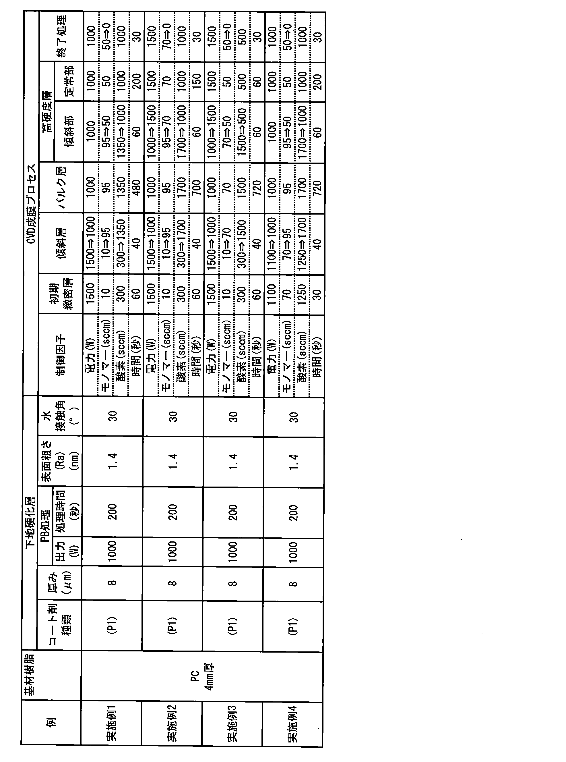
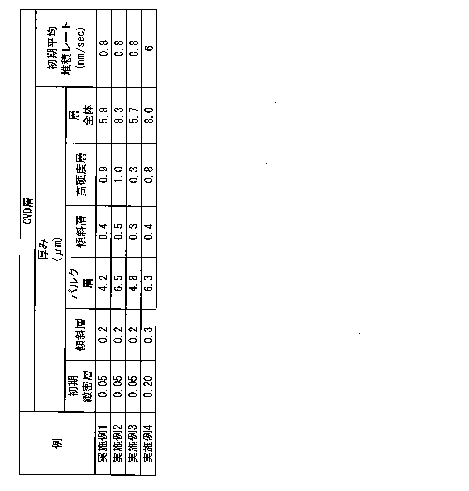


〈比較例1〉
実施例1において、下地硬化層コート剤(P1)の代わりに、下地硬化層コート剤(P2)を用いた以外は、実施例1と同様にして、ハードコート層付高分子基板を作成した。
実施例1において、下地硬化層コート剤(P1)の代わりに、下地硬化層コート剤(P2)を用いた以外は、実施例1と同様にして、ハードコート層付高分子基板を作成した。
〈比較例2〉
特許文献8の実施例6のようにしてハードコート層付高分子基板を得た。
特許文献8の実施例6のようにしてハードコート層付高分子基板を得た。
すなわち、実施例1において、酸化珪素層形成の条件を(前処理工程)Ar(アルゴン)導入量:50sccm、規定圧力:20Pa、プラズマ出力:6%、時間:60秒 、(成膜工程) TMS(トリメチルシラン)導入量:20sccm、酸素導入量:100sccm、規定圧力:25Pa、プラズマ出力:6%、時間:2000秒に変更した以外は、実施例1と同様にして、ハードコート層付高分子基板を作成した。
〈比較例3〉
実施例1において、酸化珪素層形成の条件を下記の表7に示す条件に変更した以外は、実施例1と同様にして、ハードコート層付高分子基板を作成した。
実施例1において、酸化珪素層形成の条件を下記の表7に示す条件に変更した以外は、実施例1と同様にして、ハードコート層付高分子基板を作成した。
尚、PE-CVD法による酸化珪素層全体の膜厚は、小数点第二位を四捨五入して算出すると6.0μmであった。またプラズマ処理工程とPE-CVD法による酸化珪素層の積層工程を通じ、PE-CVD法による酸化珪素層が積層される側の基板表面の最高温度は約110℃であった。各層の厚みを下記の表8に示している。
〈比較例4〉
実施例1において、酸化珪素層形成の条件を下記の表7に示す条件に変更した以外は、実施例4と同様にして、ハードコート層付高分子基板を作成した。
実施例1において、酸化珪素層形成の条件を下記の表7に示す条件に変更した以外は、実施例4と同様にして、ハードコート層付高分子基板を作成した。
尚、PE-CVD法による酸化珪素層全体の膜厚は、小数点第二位を四捨五入して算出すると6.1μmであった。またプラズマ処理工程とPE-CVD法による酸化珪素層の積層工程を通じ、PE-CVD法による酸化珪素層が積層される側の基板表面の最高温度は約110℃であった。各層の厚みを下記の表8に示している。
〈比較例5〉
実施例1において、酸化珪素層形成の条件を下記の表7に示す条件に変更した以外は、実施例1と同様にして、ハードコート層付高分子基板を作成した。
実施例1において、酸化珪素層形成の条件を下記の表7に示す条件に変更した以外は、実施例1と同様にして、ハードコート層付高分子基板を作成した。
尚、PE-CVD法による酸化珪素層全体の膜厚は、小数点第二位を四捨五入して算出すると4.3μmであった。またプラズマ処理工程とPE-CVD法による酸化珪素層の積層工程を通じ、PE-CVD法による酸化珪素層が積層される側の基板表面の最高温度は約105℃であった。各層の厚みを下記の表8に示している。
〈比較例6〉
実施例1において、酸化珪素層形成の条件を下記の表7に示す条件に変更した以外は、実施例1と同様にして、ハードコート層付高分子基板を作成した。
実施例1において、酸化珪素層形成の条件を下記の表7に示す条件に変更した以外は、実施例1と同様にして、ハードコート層付高分子基板を作成した。
尚、PE-CVD法による酸化珪素層全体の膜厚は、小数点第二位を四捨五入して算出すると5.9μmであった。またプラズマ処理工程とPE-CVD法による酸化珪素層の積層工程を通じ、PE-CVD法による酸化珪素層が積層される側の基板表面の最高温度は約110℃であった。各層の厚みを下記の表8に示している。
〈比較例7〉
特許文献5の実施例1でのようにしてハードコート層付高分子基板を得た。
特許文献5の実施例1でのようにしてハードコート層付高分子基板を得た。
すなわち、ポリカーボネート樹脂板に、活性エネルギー線硬化型プライマー組成物を、乾燥膜厚が8μmとなるようにエアスプレー塗装した。続いて、このポリカーボネート樹脂板を80℃で10分間プレヒートした後、これに、高圧水銀ランプを用いて2,000mJ/cm2の照射量で活性エネルギー線を照射し、これによって硬化塗膜層を作製した。
次いでその上に、無機物質層を膜厚が5μmとなるようプラズマCVD装置を用いて積層させて、ハードコート層付高分子基板を得た。
〈比較例8〉
特許文献6の実施例1でのようにしてハードコート層付高分子基板を得た。
特許文献6の実施例1でのようにしてハードコート層付高分子基板を得た。
すなわち、最初に基材フィルムである、厚みが188μmのPMMAフィルム(商品名「RT050」株式会社クラレ製)の表面に第1ハードコート層としてUV硬化樹脂(商品名「UVHC7800」モメンティブ・パフォーマンス・マテリアルズ・ジャパン合同会社製)を、厚みが15μmとなるように、グラビア印刷法により積層し、積層したら、60℃の雰囲気下で1分間乾燥させた後、UVを照射してこれを硬化させた。
その表面にアンカーコート層として、有機無機ハイブリッド樹脂(製品名「NH-1000G」日本曹達株式会社製)をバーコード法により積層させた。この際、原料樹脂にフィラー(商品名「NH-9100S」日本曹達株式会社製)を混合させた。
そして第2ハードコート層として、HMDSO(Hexamethyldisilozane)(信越化学工業株式会社製)を材料としたプラズマ蒸着層を積層して、ハードコート層付高分子基板を得た。
ここで、アンカーコート層の膜厚を7.0μmとし、フィラーの添加量を2.5%とし、かつ第2ハードコート層の厚みを150nmとした。
〈比較例9〉
特許文献7の実施例1でのようにしてハードコート層付高分子基板を得た。
特許文献7の実施例1でのようにしてハードコート層付高分子基板を得た。
すなわち、複合コーティング組成物を、表面清浄化したレキサン(Lexan)ポリカーボネート板(150mm×150mm×4mm厚)に硬化塗膜として約9~14μmになるようにフローコートし、120℃にて60分加熱硬化させ、中間層を得た。
更に該塗膜上に、プラズマ重合によりケイ素、酸素、炭素及び水素原子からなる被膜を最表層として積層、積層体を得た。具体的には、まずプラズマ重合の前に、複合コーティング組成物の硬化被膜が形成された基材はイソプロピルアルコール及び脱イオン水を用い、リントを含んでいない布により手によって清浄にした。次いで、真空チャンバー内において、連続的な両サイド膨張熱プラズマプロセスによりプラズマ重合を行った。2つのプラズマコーティング位置は、超音速でアルゴンプラズマジェットを創成する膨張熱プラズマ源列よりなる。プラズマジェットはプラズマコーティング位置で膨張し、チャンバー内に直接注入された有機ケイ素試薬および酸化剤と反応した。この有機ケイ素試薬はオクタメチルシクロテトラシロキサン(Gelest社製)であり、酸化剤は工業用グレードの酸素99%(Airgas社製)であった。基材は連続的にチャンバーを通って移送され、コーティング位置に入る前に約40~70℃に加熱された。
比較例1~9に関して、酸化珪素層(CVD層)の化学組成SixCyHzの詳細を下記の表9に示し、ナノインデンテーション測定、表面粗さ、及び赤外線吸収ピーク強度比の詳細を下記の表10に示し、かつ、ハードコート層付高分子基板の性能評価の結果を下記の表11に示している。

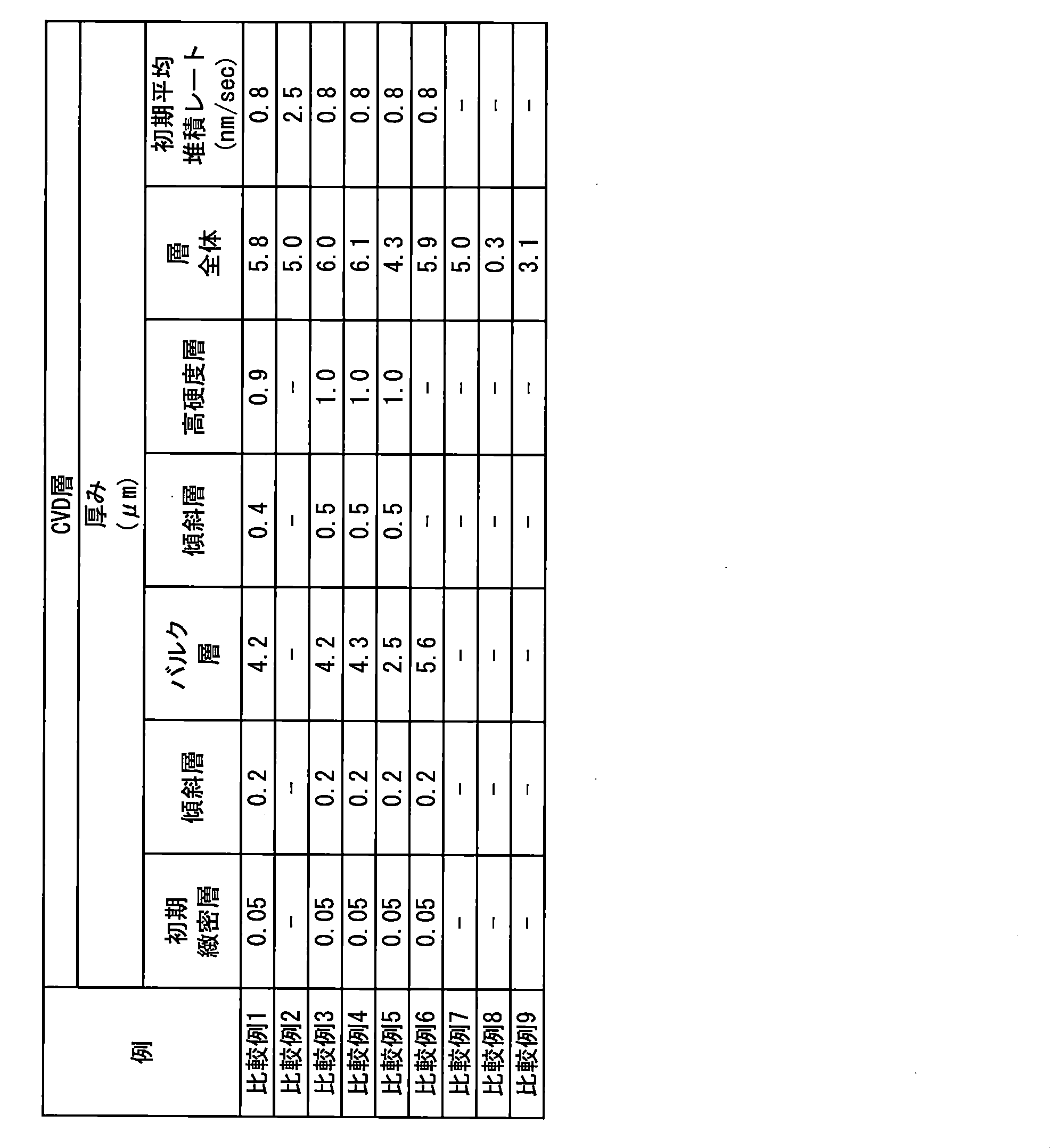
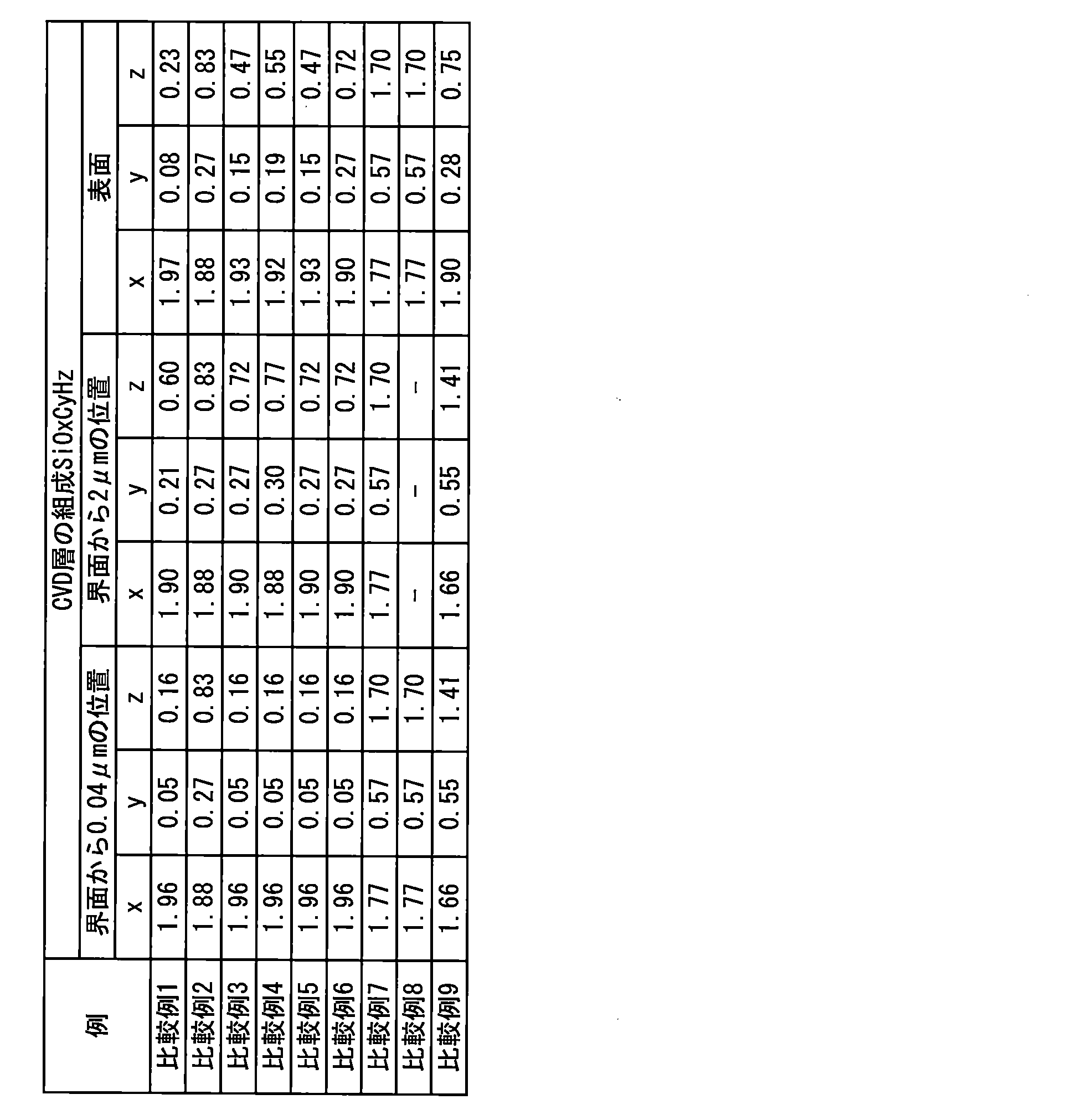
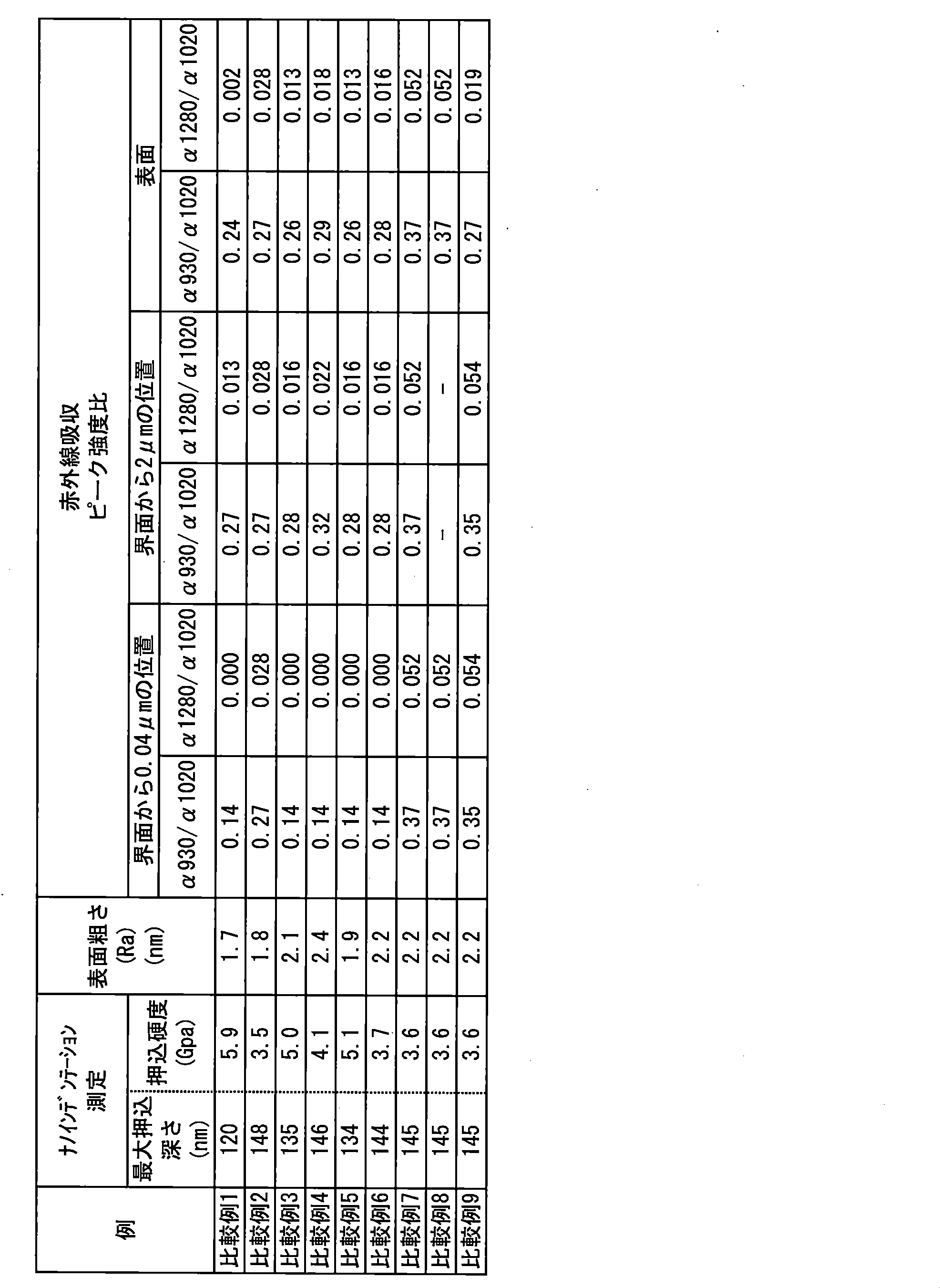

上記の表6及び11において、初期性能、耐沸水性、耐熱性(110℃1000hr、130℃1000hr)耐候性(2000hr、4000hr、8000hr)の「外観」の評価について、剥離もクラックも生じかなった場合を「A」とし、剥離は生じなかったがクラックが生じた場合を「B」とし、部分的な剥離が生じた場合を「C」とし、クラックが生じ、かつ部分的に剥離が生じた場合を「D」とした。
また、上記の表6及び11において、「外観」以外の評価について、良好であった場合を「A」とし、不良であった場合を「D」とした。
上記の表を簡易にまとめた表を以下に示す:

表12の「耐摩耗性」は、表5及び表10に記載の酸化珪素層のナノインデンテーション測定の結果と、表6及び表11に記載のテーバー摩耗性の結果とから評価した。「耐摩耗性」の評価は、押込硬度が4.5GPa以上であり、かつテーバー摩耗性の△Hが1.0%以下である場合を「VG」;押込硬度が4.5GPa以上であるか又はテーバー摩耗性の△Hが1.0%以下である場合を「G」;押込硬度が4.5GPa以下であり、かつテーバー摩耗性の△Hが1.0%以上である場合を「P」とした。
表12の「耐沸水性」、「耐熱性」及び「耐候性」は、表6及び表11に記載のそれぞれの評価を3段階に分けて、「VG」、「G」、及び「P」とした。
〈実施例および比較例の評価〉
上記の表4~6及び9~12からは、特定の下地硬化層を用いて、下地硬化層と接する上記酸化珪素層の界面から厚み方向に0.04μmの位置および表面が、それぞれ特定の化学組成SiOxCyHzおよび赤外線吸光度の比を満たすときに、好ましい結果が得られることが理解される。これに対して、これらのいずれかを満たさない場合には、好ましい結果は得られなかった。具体的には、表2、5、6、及び12からは下記の点が理解された。
上記の表4~6及び9~12からは、特定の下地硬化層を用いて、下地硬化層と接する上記酸化珪素層の界面から厚み方向に0.04μmの位置および表面が、それぞれ特定の化学組成SiOxCyHzおよび赤外線吸光度の比を満たすときに、好ましい結果が得られることが理解される。これに対して、これらのいずれかを満たさない場合には、好ましい結果は得られなかった。具体的には、表2、5、6、及び12からは下記の点が理解された。
(1)実施例1および2について
実施例1および2ではPE-CVD法による酸化珪素層の形成条件のみが異なっているが、耐候性、テーバー摩耗性、高硬度、沸水性能、耐水性能、耐熱性能とも良好な結果が得られている。
実施例1および2ではPE-CVD法による酸化珪素層の形成条件のみが異なっているが、耐候性、テーバー摩耗性、高硬度、沸水性能、耐水性能、耐熱性能とも良好な結果が得られている。
これは、実施例1および2の下地硬化層は、多官能アクリレート10~90重量部、複合樹脂(A)を含有する珪素化合物加水分解縮合物90~10重量部を含み、かつ厚みが1~20μmであり、かつ酸化珪素層が、少なくとも、下地硬化層と接する酸化珪素層の界面から厚み方向に0.04μmの位置において下記(a1)要件を満たし、かつ表面において下記(a3)の要件を満たしていることによるものである:
(a1)化学組成をSiOxCyHzで表した際に、xが1.93~1.98の範囲にあり、yが0.04~0.15の範囲にあり、かつzが0.10~0.50の範囲にあること、
(a3)化学組成をSiOxCyHzで表した際に、xが1.94~2.02の範囲にあり、yが0.05~0.16の範囲にあり、かつzが0.20~0.50の範囲にあること。
(a1)化学組成をSiOxCyHzで表した際に、xが1.93~1.98の範囲にあり、yが0.04~0.15の範囲にあり、かつzが0.10~0.50の範囲にあること、
(a3)化学組成をSiOxCyHzで表した際に、xが1.94~2.02の範囲にあり、yが0.05~0.16の範囲にあり、かつzが0.20~0.50の範囲にあること。
さらに、これは、実施例1および2の下地硬化層が、下地硬化層と酸化珪素層の界面から厚み方向に0.04μmの位置において、下記(a1)~(c1)に記載の好ましい要件の全てを満たし、かつ界面と反対側の表面において、下記(b3)~(c3)に記載の好ましい要件の全てを満たしていることによるものである:
(a1)化学組成をSiOxCyHzで表した際に、xが1.93~1.98の範囲にあり、yが0.04~0.15の範囲にあり、かつzが0.10~0.45の範囲にあること、
(b1)波数930cm-1と1020cm-1の赤外線吸光度の比(α930/α1020)が、0.10~0.20の範囲にあること、
(c1)波数1280cm-1と1020cm-1の赤外線吸光度の比(α1280/α1020)が、0~0.005の範囲にあること、
(b3)波数930cm-1と1020cm-1の赤外線吸光度の比(α930/α1020)が、0.15~0.25の範囲にあること、
(c3)波数1280cm-1と1020cm-1の赤外線吸光度の比(α1280/α1020)が、0.002~0.020の範囲にあること。
(a1)化学組成をSiOxCyHzで表した際に、xが1.93~1.98の範囲にあり、yが0.04~0.15の範囲にあり、かつzが0.10~0.45の範囲にあること、
(b1)波数930cm-1と1020cm-1の赤外線吸光度の比(α930/α1020)が、0.10~0.20の範囲にあること、
(c1)波数1280cm-1と1020cm-1の赤外線吸光度の比(α1280/α1020)が、0~0.005の範囲にあること、
(b3)波数930cm-1と1020cm-1の赤外線吸光度の比(α930/α1020)が、0.15~0.25の範囲にあること、
(c3)波数1280cm-1と1020cm-1の赤外線吸光度の比(α1280/α1020)が、0.002~0.020の範囲にあること。
(2)実施例3について
実施例3は、実施例1の条件と比較してPE-CVD法による酸化珪素層の形成条件のみが異なっているが、少なくとも、上記「(1)実施例1および2について」で記載した要件を満たしているため、テーバー摩耗性、高硬度、沸水性能、耐水性能、耐熱性能とも良好な結果が得られ、促進耐候性についても良好な結果が得られている。実施例3は、実施例1より直接的に投入電力を高くして投入電力の比率を上げおり、緻密な高硬度層が形成されているため、高硬度について実施例1より良好な結果が得られている。
実施例3は、実施例1の条件と比較してPE-CVD法による酸化珪素層の形成条件のみが異なっているが、少なくとも、上記「(1)実施例1および2について」で記載した要件を満たしているため、テーバー摩耗性、高硬度、沸水性能、耐水性能、耐熱性能とも良好な結果が得られ、促進耐候性についても良好な結果が得られている。実施例3は、実施例1より直接的に投入電力を高くして投入電力の比率を上げおり、緻密な高硬度層が形成されているため、高硬度について実施例1より良好な結果が得られている。
(3)実施例4について
実施例4は、実施例1の条件とPE-CVD法による酸化珪素層の形成条件のみが異なっているが、上記「(1)実施例1および2について」で記載した要件のうち、(a1)~(c1)に記載の好ましい要件を満たしていない。これにより、実施例4は、極めて高度な耐摩耗性は得られているものの、耐沸水性及び耐熱性については、実施例1の方が良好な結果となっている。
実施例4は、実施例1の条件とPE-CVD法による酸化珪素層の形成条件のみが異なっているが、上記「(1)実施例1および2について」で記載した要件のうち、(a1)~(c1)に記載の好ましい要件を満たしていない。これにより、実施例4は、極めて高度な耐摩耗性は得られているものの、耐沸水性及び耐熱性については、実施例1の方が良好な結果となっている。
(5)実施例1と比較例1との対比
実施例1と比較例1は、下地硬化層のプラズマ処理条件、PE-CVD法による酸化珪素層の形成条件で同一である(表2及び7を参照されたい)。しかしながら、比較例1では、耐摩耗性、高硬度、及び耐熱性等で良好な結果が得られたものの、優れた耐候性は得られなかった。比較例1では、下地硬化層コート剤の珪素化合物加水分解縮合物に複合樹脂(A)を含有しておらず、請求項1で規定する要件を満たしていない。この結果として、優れた耐候性、耐摩耗性、高硬度、及び耐熱性を両立するハードコート付高分子基材が得られなかった。
実施例1と比較例1は、下地硬化層のプラズマ処理条件、PE-CVD法による酸化珪素層の形成条件で同一である(表2及び7を参照されたい)。しかしながら、比較例1では、耐摩耗性、高硬度、及び耐熱性等で良好な結果が得られたものの、優れた耐候性は得られなかった。比較例1では、下地硬化層コート剤の珪素化合物加水分解縮合物に複合樹脂(A)を含有しておらず、請求項1で規定する要件を満たしていない。この結果として、優れた耐候性、耐摩耗性、高硬度、及び耐熱性を両立するハードコート付高分子基材が得られなかった。
(6)実施例1と比較例2との対比
実施例1と比較例2は、PE-CVD法による酸化珪素層の形成条件のみが異なっている。比較例2は、酸化珪素層の表面の(a)化学組成SiOxCyHzにおいて、xが、上記「(1)実施例1および2について」で記載した要件の範囲外であり、かつ表面の(b3)赤外線吸光度の比(α930/α1020)も好ましい範囲を外れているため、耐摩耗性が不十分であった。さらに、耐熱性、沸水性能も良好な結果が得られなかった。
実施例1と比較例2は、PE-CVD法による酸化珪素層の形成条件のみが異なっている。比較例2は、酸化珪素層の表面の(a)化学組成SiOxCyHzにおいて、xが、上記「(1)実施例1および2について」で記載した要件の範囲外であり、かつ表面の(b3)赤外線吸光度の比(α930/α1020)も好ましい範囲を外れているため、耐摩耗性が不十分であった。さらに、耐熱性、沸水性能も良好な結果が得られなかった。
(7)実施例1と比較例3、5との対比
実施例1と比較例3、5では、PE-CVD法による酸化珪素層の形成条件のみが異なっている。比較例3、5は、酸化珪素層の表面の(a3)化学組成SiOxCyHzにおいて、xが、上記「(1)実施例1~4について」で記載した要件の範囲外であり、かつ表面の(b3)赤外線吸光度の比(α930/α1020)も好ましい範囲を外れているため、耐摩耗性が不十分であった。
実施例1と比較例3、5では、PE-CVD法による酸化珪素層の形成条件のみが異なっている。比較例3、5は、酸化珪素層の表面の(a3)化学組成SiOxCyHzにおいて、xが、上記「(1)実施例1~4について」で記載した要件の範囲外であり、かつ表面の(b3)赤外線吸光度の比(α930/α1020)も好ましい範囲を外れているため、耐摩耗性が不十分であった。
(8)実施例1と比較例4との対比
実施例1と比較例4とは、PE-CVD法による酸化珪素層の形成条件のみが異なっている。比較例4は、酸化珪素層の表面の(a3)化学組成SiOxCyHzにおいて、x、yおよびzが、上記「(1)実施例1~4について」で記載した要件の範囲外であり、かつその表面の(b3)赤外線吸光度の比(α930/α1020)が好ましい範囲を外れているため、高硬度が不十分であった。
実施例1と比較例4とは、PE-CVD法による酸化珪素層の形成条件のみが異なっている。比較例4は、酸化珪素層の表面の(a3)化学組成SiOxCyHzにおいて、x、yおよびzが、上記「(1)実施例1~4について」で記載した要件の範囲外であり、かつその表面の(b3)赤外線吸光度の比(α930/α1020)が好ましい範囲を外れているため、高硬度が不十分であった。
(9)実施例1と比較例6との対比
実施例1と比較例6とは、PE-CVD法による酸化珪素層の形成条件のみが異なっており、比較例6は、高硬度層が存在せず、バルク層で酸化珪素層の形成が終了しており、酸化珪素層の表面の(a3)化学組成SiOxCyHzにおいて、x、yおよびzが上記「(1)実施例1~4について」で記載した要件の範囲外であり、(b3)赤外線吸光度の比(α930/α1020)が好ましい範囲を外れているため、テーバー摩耗性、高硬度、耐沸水性、耐熱性が不十分であった。
実施例1と比較例6とは、PE-CVD法による酸化珪素層の形成条件のみが異なっており、比較例6は、高硬度層が存在せず、バルク層で酸化珪素層の形成が終了しており、酸化珪素層の表面の(a3)化学組成SiOxCyHzにおいて、x、yおよびzが上記「(1)実施例1~4について」で記載した要件の範囲外であり、(b3)赤外線吸光度の比(α930/α1020)が好ましい範囲を外れているため、テーバー摩耗性、高硬度、耐沸水性、耐熱性が不十分であった。
(10)実施例1と比較例7及び8との対比
実施例1と比較例7及び8とは、下地硬化層の種類およびPE-CVD法による酸化珪素層の形成条件が異なっており、比較例7及び8は、下地硬化層との界面から0.04μmの酸化珪素層の化学組成SiOxCyHz(a1)において、x、yおよびzが上記「(1)実施例1~4について」で記載した要件の範囲外である。また、下地硬化層との界面から0.04μmの位置において、酸化珪素層の(b1)赤外線吸光度の比(α930/α1020)および(c1)赤外線吸光度の比(α1280/α1020)が好ましい範囲を外れている。さらに、酸化珪素層の表面の化学組成SiOxCyHz(a3)において、x、yおよびzが上記要件の範囲外であり、(b3)赤外線吸光度の比(α930/α1020)および(c3)赤外線吸光度の比(α1280/α1020)が好ましい範囲を外れているため、テーバー摩耗性、高硬度、耐沸水性、耐熱性が不十分であった。
実施例1と比較例7及び8とは、下地硬化層の種類およびPE-CVD法による酸化珪素層の形成条件が異なっており、比較例7及び8は、下地硬化層との界面から0.04μmの酸化珪素層の化学組成SiOxCyHz(a1)において、x、yおよびzが上記「(1)実施例1~4について」で記載した要件の範囲外である。また、下地硬化層との界面から0.04μmの位置において、酸化珪素層の(b1)赤外線吸光度の比(α930/α1020)および(c1)赤外線吸光度の比(α1280/α1020)が好ましい範囲を外れている。さらに、酸化珪素層の表面の化学組成SiOxCyHz(a3)において、x、yおよびzが上記要件の範囲外であり、(b3)赤外線吸光度の比(α930/α1020)および(c3)赤外線吸光度の比(α1280/α1020)が好ましい範囲を外れているため、テーバー摩耗性、高硬度、耐沸水性、耐熱性が不十分であった。
(11)実施例1と比較例9との対比
実施例1と比較例9とは、下地硬化層の種類およびPE-CVD法による酸化珪素層の形成条件が異なっており、比較例11は、下地硬化層との界面から0.04μmの酸化珪素層の(a1)化学組成SiOxCyHzにおいて、x、yおよびzが上記「(1)実施例1~4について」で記載した要件の範囲外であり、(b1)赤外線吸光度の比(α930/α1020)および(c1)赤外線吸光度の比(α1280/α1020)が好ましい範囲を外れている。また、酸化珪素層の表面の(a3)化学組成SiOxCyHzにおいて、x、yおよびzが上記要件の範囲外であり、(b3)赤外線吸光度の比(α930/α1020)が好ましい範囲を外れているため、高硬度、耐沸水性、耐熱性が不十分であった。
実施例1と比較例9とは、下地硬化層の種類およびPE-CVD法による酸化珪素層の形成条件が異なっており、比較例11は、下地硬化層との界面から0.04μmの酸化珪素層の(a1)化学組成SiOxCyHzにおいて、x、yおよびzが上記「(1)実施例1~4について」で記載した要件の範囲外であり、(b1)赤外線吸光度の比(α930/α1020)および(c1)赤外線吸光度の比(α1280/α1020)が好ましい範囲を外れている。また、酸化珪素層の表面の(a3)化学組成SiOxCyHzにおいて、x、yおよびzが上記要件の範囲外であり、(b3)赤外線吸光度の比(α930/α1020)が好ましい範囲を外れているため、高硬度、耐沸水性、耐熱性が不十分であった。
本発明のハードコート層付高分子基板は、無機ガラス並みの優れた表面耐摩耗性を有し、厳しい使用環境下でも長期的に使用する事のできる高度な耐環境性を併せ持っており、例えば、自動車窓材、建築部材、太陽電池の表面保護板等に利用する事ができ、極めて有用である。
1 真空容器
2 電源
3 マッチングボックス
4 排気口
5 真空ポンプ
6A 冷却媒体
7 反応ガス
10 カソード電極
14 シールド部品
20 アノード電極
30、31 被処理基板
40、41 ガス導入ヘッド
40A、41A 吹き出し孔
40B、41B 流入孔
50 高分子基板
60 接着層
70 下地硬化層
80 PE-CVD法による酸化珪素層
2 電源
3 マッチングボックス
4 排気口
5 真空ポンプ
6A 冷却媒体
7 反応ガス
10 カソード電極
14 シールド部品
20 アノード電極
30、31 被処理基板
40、41 ガス導入ヘッド
40A、41A 吹き出し孔
40B、41B 流入孔
50 高分子基板
60 接着層
70 下地硬化層
80 PE-CVD法による酸化珪素層
Claims (15)
- 高分子基板、下地硬化層、および酸化珪素層がこの順に直接積層されたハードコート層付高分子基板であって、
上記下地硬化層は、厚みが1~20μmであり、かつ珪素化合物加水分解縮合物を含み、該珪素化合物加水分解縮合物が、一般式(1)および/または一般式(2)で表される構造単位と、シラノール基および/または加水分解性シリル基とを有するポリシロキサンセグメント(a1)と、ビニル系重合体セグメント(a2)とが、一般式(3)で表される結合により結合された複合樹脂(A)を含有し、
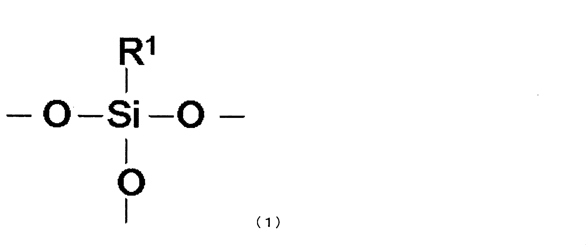
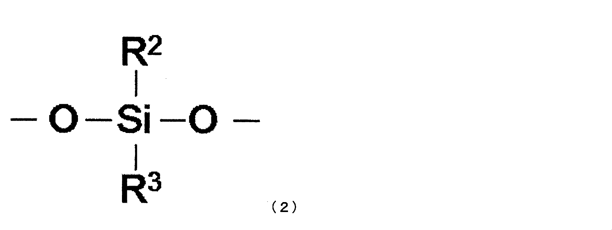
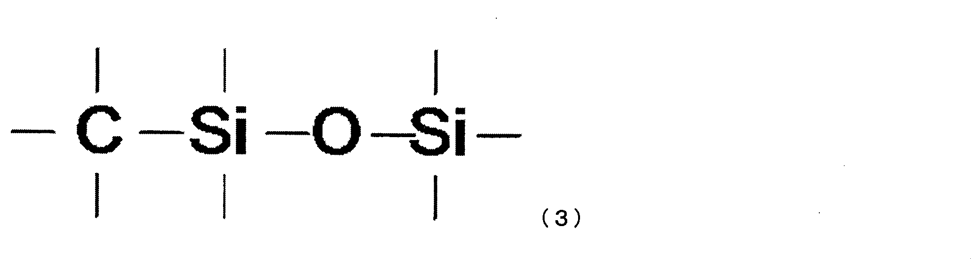
上記酸化珪素層は、上記下地硬化層と上記酸化珪素層との界面から厚み方向に0.04μmの位置において、下記(a1)を満たし、かつ前記界面と反対側の表面において下記(a3)を満たす、
ハードコート層付高分子基板:
(a1)化学組成をSiOxCyHzで表した際に、xが1.93~1.98の範囲にあり、yが0.04~0.15の範囲にあり、かつzが0.10~0.50の範囲にあること、
(a3)化学組成をSiOxCyHzで表した際に、xが1.94~2.02の範囲にあり、yが0.05~0.16の範囲にあり、かつzが0.20~0.50の範囲にあること。 - 前記酸化珪素層は、前記下地硬化層と前記酸化珪素層の界面から厚み方向に0.04μmの位置において下記(a1)~(c1)のすべての要件を満たし、かつ前記界面と反対側の表面において下記(b3)~(c3)のすべての要件を満たす、
請求項1に記載のハードコート層付高分子基板:
(a1)化学組成をSiOxCyHzで表した際に、xが1.93~1.98の範囲にあり、yが0.04~0.15の範囲にあり、かつzが0.10~0.45の範囲にあること、
(b1)波数930cm-1と1020cm-1の赤外線吸光度の比(α930/α1020)が、0.10~0.20の範囲にあること、
(c1)波数1280cm-1と1020cm-1の赤外線吸光度の比(α1280/α1020)が、0~0.005の範囲にあること、
(b3)波数930cm-1と1020cm-1の赤外線吸光度の比(α930/α1020)が、0.15~0.25の範囲にあること、
(c3)波数1280cm-1と1020cm-1の赤外線吸光度の比(α1280/α1020)が、0.002~0.020の範囲にあること。 - 上記(a3)におけるyが(a1)におけるyよりも、0.02~0.10大きく、かつ上記(a3)におけるzが(a1)におけるzよりも、0.05~0.25大きい、請求項1~2のいずれか一項に記載のハードコート層付高分子基板。
- 上記下地硬化層は、多官能アクリレート10~90重量部及び珪素化合物加水分解縮合物90~10重量部を含む、請求項1~3のいずれか一項に記載のハードコート層付高分子基板。
- 上記下地硬化層は、水酸基、アミノ基、カルボキシル基およびアルコキシシリル基から選ばれる少なくとも1種を化合物中に0.1~5mol/kg含む(メタ)アクリル樹脂を含有する、請求項4に記載のハードコート層付高分子基板。
- 上記下地硬化層は、無機酸化物微粒子をさらに含む、請求項1~5のいずれか一項に記載のハードコート層付高分子基板。
- 上記高分子基板がポリカーボネート樹脂基板である、請求項1~6のいずれか一項に記載のハードコート層付高分子基板。
- 上記酸化珪素層がプラズマCVD層である、請求項1~7のいずれか一項に記載のハードコート層付高分子基板。
- 上記酸化珪素層は、厚みが2.5~9μmであり、上記下地硬化層と上記酸化珪素層との界面から厚み方向に2.0μmの位置において下記(a2)~(c2)のすべての要件を満たす、請求項1~8のいずれか一項に記載のハードコート層付高分子基板:
(a2)化学組成をSiOxCyHzで表した際に、xが1.81~1.90の範囲にあり、yが0.15~0.32の範囲にあり、かつzが0.45~0.90の範囲にあること、
(b2)波数930cm-1と1020cm-1の赤外線吸光度の比(α930/α1020)が、0.21~0.36の範囲にあること、
(c2)波数1280cm-1と1020cm-1の赤外線吸光度の比(α1280/α1020)が、0.010~0.040の範囲にあること。 - 上記酸化珪素層の(a2)~(c2)のすべての要件を満たす部分の厚みが、1.5~8.5μmである、請求項9に記載のハードコート層付高分子基板。
- 上記酸化珪素層の(a3)~(c3)のすべての要件を満たす部分が、0.1~1.4μmの厚みで前記表面に存在する、請求項9又は10に記載のハードコート層付高分子基板。
- 上記酸化珪素層の(a1)~(c1)のすべての要件を満たす部分と、上記酸化珪素層の(a2)~(c2)のすべての要件を満たす部分との間には、上記x、上記y、上記z、上記α930/α1020、及び/又は上記α1280/α1020の値の変化が、傾斜的である傾斜層が、さらに含まれている、請求項9~11のいずれか一項に記載のハードコート層付高分子基板。
- 上記酸化珪素層の(a2)~(c2)のすべての要件を満たす部分と、上記酸化珪素層の(a3)~(c3)のすべての要件を満たす部分との間には、上記x、上記y、上記z、上記α930/α1020、及び/又は上記α1280/α1020の値の変化が、傾斜的である傾斜層が、さらに含まれている、請求項9~12のいずれか一項に記載のハードコート層付高分子基板。
- 上記酸化珪素層の厚みが0.1~2.5μmである、請求項1~8のいずれか一項に記載のハードコート層付高分子基板。
- 上記酸化珪素層の(a1)~(c1)のすべての要件を満たす部分と、上記酸化珪素層の(a3)~(c3)のすべての要件を満たす部分との間には、上記x、上記y、上記z、上記α930/α1020、及び/又は上記α1280/α1020の値の変化が、傾斜的である傾斜層が、さらに含まれている、請求項14に記載のハードコート層付高分子基板。
Priority Applications (1)
| Application Number | Priority Date | Filing Date | Title |
|---|---|---|---|
| JP2020550462A JP7159336B2 (ja) | 2018-10-02 | 2019-10-01 | ハードコート層付高分子基板 |
Applications Claiming Priority (2)
| Application Number | Priority Date | Filing Date | Title |
|---|---|---|---|
| JP2018-187522 | 2018-10-02 | ||
| JP2018187522 | 2018-10-02 |
Publications (1)
| Publication Number | Publication Date |
|---|---|
| WO2020071379A1 true WO2020071379A1 (ja) | 2020-04-09 |
Family
ID=70055593
Family Applications (1)
| Application Number | Title | Priority Date | Filing Date |
|---|---|---|---|
| PCT/JP2019/038783 Ceased WO2020071379A1 (ja) | 2018-10-02 | 2019-10-01 | ハードコート層付高分子基板 |
Country Status (2)
| Country | Link |
|---|---|
| JP (1) | JP7159336B2 (ja) |
| WO (1) | WO2020071379A1 (ja) |
Cited By (4)
| Publication number | Priority date | Publication date | Assignee | Title |
|---|---|---|---|---|
| JPWO2021172356A1 (ja) * | 2020-02-26 | 2021-09-02 | ||
| CN116265501A (zh) * | 2021-12-16 | 2023-06-20 | 浙江省化工研究院有限公司 | 一种倍半硅氧烷改性乙烯-三氟氯乙烯树脂 |
| WO2025013853A1 (ja) * | 2023-07-11 | 2025-01-16 | 日東電工株式会社 | フィルムおよび積層体 |
| WO2025013854A1 (ja) * | 2023-07-11 | 2025-01-16 | 日東電工株式会社 | フィルムおよび積層体 |
Citations (6)
| Publication number | Priority date | Publication date | Assignee | Title |
|---|---|---|---|---|
| JP2006328354A (ja) * | 2005-03-08 | 2006-12-07 | Dainippon Ink & Chem Inc | 紫外線硬化性樹脂組成物、紫外線硬化性塗料及び塗装物。 |
| JP2014531334A (ja) * | 2011-08-26 | 2014-11-27 | エグザテック・リミテッド・ライアビリティー・カンパニーExatec,LLC. | 有機樹脂積層体、その製造及び使用方法、並びに有機樹脂積層体を含む物品 |
| JP2015093400A (ja) * | 2013-11-11 | 2015-05-18 | Dic株式会社 | 積層体 |
| WO2015147295A1 (ja) * | 2014-03-27 | 2015-10-01 | 帝人株式会社 | ハードコート層付高分子基板およびその製造方法 |
| WO2016068236A1 (ja) * | 2014-10-30 | 2016-05-06 | Dic株式会社 | 積層体 |
| JP2016216589A (ja) * | 2015-05-19 | 2016-12-22 | Dic株式会社 | ポリシロキサン、樹脂組成物、塗料及び積層体 |
-
2019
- 2019-10-01 WO PCT/JP2019/038783 patent/WO2020071379A1/ja not_active Ceased
- 2019-10-01 JP JP2020550462A patent/JP7159336B2/ja active Active
Patent Citations (6)
| Publication number | Priority date | Publication date | Assignee | Title |
|---|---|---|---|---|
| JP2006328354A (ja) * | 2005-03-08 | 2006-12-07 | Dainippon Ink & Chem Inc | 紫外線硬化性樹脂組成物、紫外線硬化性塗料及び塗装物。 |
| JP2014531334A (ja) * | 2011-08-26 | 2014-11-27 | エグザテック・リミテッド・ライアビリティー・カンパニーExatec,LLC. | 有機樹脂積層体、その製造及び使用方法、並びに有機樹脂積層体を含む物品 |
| JP2015093400A (ja) * | 2013-11-11 | 2015-05-18 | Dic株式会社 | 積層体 |
| WO2015147295A1 (ja) * | 2014-03-27 | 2015-10-01 | 帝人株式会社 | ハードコート層付高分子基板およびその製造方法 |
| WO2016068236A1 (ja) * | 2014-10-30 | 2016-05-06 | Dic株式会社 | 積層体 |
| JP2016216589A (ja) * | 2015-05-19 | 2016-12-22 | Dic株式会社 | ポリシロキサン、樹脂組成物、塗料及び積層体 |
Cited By (9)
| Publication number | Priority date | Publication date | Assignee | Title |
|---|---|---|---|---|
| JPWO2021172356A1 (ja) * | 2020-02-26 | 2021-09-02 | ||
| WO2021172356A1 (ja) * | 2020-02-26 | 2021-09-02 | 富士フイルム株式会社 | ハードコート積層体 |
| JP7440607B2 (ja) | 2020-02-26 | 2024-02-28 | 富士フイルム株式会社 | ハードコート積層体 |
| US12577407B2 (en) | 2020-02-26 | 2026-03-17 | Fujifilm Corporation | Hard coat laminate |
| CN116265501A (zh) * | 2021-12-16 | 2023-06-20 | 浙江省化工研究院有限公司 | 一种倍半硅氧烷改性乙烯-三氟氯乙烯树脂 |
| WO2025013853A1 (ja) * | 2023-07-11 | 2025-01-16 | 日東電工株式会社 | フィルムおよび積層体 |
| WO2025013854A1 (ja) * | 2023-07-11 | 2025-01-16 | 日東電工株式会社 | フィルムおよび積層体 |
| JP2025011541A (ja) * | 2023-07-11 | 2025-01-24 | 日東電工株式会社 | フィルムおよび積層体 |
| JP2025011540A (ja) * | 2023-07-11 | 2025-01-24 | 日東電工株式会社 | フィルムおよび積層体 |
Also Published As
| Publication number | Publication date |
|---|---|
| JP7159336B2 (ja) | 2022-10-24 |
| JPWO2020071379A1 (ja) | 2021-09-24 |
Similar Documents
| Publication | Publication Date | Title |
|---|---|---|
| US11028284B2 (en) | Polymer substrate with hardcoat layer, and manufacturing method for same | |
| US9758630B2 (en) | Polymer substrate with hard coat layer and manufacturing method for such polymer substrate | |
| KR102487752B1 (ko) | 적층체 | |
| JP7159336B2 (ja) | ハードコート層付高分子基板 | |
| JP6749476B2 (ja) | ハードコート層付高分子基板 | |
| JP2012232591A (ja) | 微小亀裂耐性の向上した積層品及びその製造方法 | |
| JP6349683B2 (ja) | 積層体 | |
| US10682669B2 (en) | Method for manufacturing laminate |
Legal Events
| Date | Code | Title | Description |
|---|---|---|---|
| 121 | Ep: the epo has been informed by wipo that ep was designated in this application |
Ref document number: 19870010 Country of ref document: EP Kind code of ref document: A1 |
|
| ENP | Entry into the national phase |
Ref document number: 2020550462 Country of ref document: JP Kind code of ref document: A |
|
| NENP | Non-entry into the national phase |
Ref country code: DE |
|
| 122 | Ep: pct application non-entry in european phase |
Ref document number: 19870010 Country of ref document: EP Kind code of ref document: A1 |