WO2020071223A1 - 光電変換素子及びその製造方法 - Google Patents
光電変換素子及びその製造方法Info
- Publication number
- WO2020071223A1 WO2020071223A1 PCT/JP2019/037781 JP2019037781W WO2020071223A1 WO 2020071223 A1 WO2020071223 A1 WO 2020071223A1 JP 2019037781 W JP2019037781 W JP 2019037781W WO 2020071223 A1 WO2020071223 A1 WO 2020071223A1
- Authority
- WO
- WIPO (PCT)
- Prior art keywords
- group
- photoelectric conversion
- conversion element
- semiconductor material
- transport layer
- Prior art date
- Legal status (The legal status is an assumption and is not a legal conclusion. Google has not performed a legal analysis and makes no representation as to the accuracy of the status listed.)
- Ceased
Links
Images


Classifications
-
- H—ELECTRICITY
- H10—SEMICONDUCTOR DEVICES; ELECTRIC SOLID-STATE DEVICES NOT OTHERWISE PROVIDED FOR
- H10K—ORGANIC ELECTRIC SOLID-STATE DEVICES
- H10K39/00—Integrated devices, or assemblies of multiple devices, comprising at least one organic radiation-sensitive element covered by group H10K30/00
- H10K39/30—Devices controlled by radiation
- H10K39/32—Organic image sensors
-
- H—ELECTRICITY
- H10—SEMICONDUCTOR DEVICES; ELECTRIC SOLID-STATE DEVICES NOT OTHERWISE PROVIDED FOR
- H10F—INORGANIC SEMICONDUCTOR DEVICES SENSITIVE TO INFRARED RADIATION, LIGHT, ELECTROMAGNETIC RADIATION OF SHORTER WAVELENGTH OR CORPUSCULAR RADIATION
- H10F39/00—Integrated devices, or assemblies of multiple devices, comprising at least one element covered by group H10F30/00, e.g. radiation detectors comprising photodiode arrays
- H10F39/10—Integrated devices
- H10F39/12—Image sensors
-
- H—ELECTRICITY
- H10—SEMICONDUCTOR DEVICES; ELECTRIC SOLID-STATE DEVICES NOT OTHERWISE PROVIDED FOR
- H10K—ORGANIC ELECTRIC SOLID-STATE DEVICES
- H10K30/00—Organic devices sensitive to infrared radiation, light, electromagnetic radiation of shorter wavelength or corpuscular radiation
- H10K30/80—Constructional details
- H10K30/81—Electrodes
-
- H—ELECTRICITY
- H10—SEMICONDUCTOR DEVICES; ELECTRIC SOLID-STATE DEVICES NOT OTHERWISE PROVIDED FOR
- H10K—ORGANIC ELECTRIC SOLID-STATE DEVICES
- H10K85/00—Organic materials used in the body or electrodes of devices covered by this subclass
- H10K85/20—Carbon compounds, e.g. carbon nanotubes or fullerenes
- H10K85/211—Fullerenes, e.g. C60
-
- G—PHYSICS
- G06—COMPUTING OR CALCULATING; COUNTING
- G06F—ELECTRIC DIGITAL DATA PROCESSING
- G06F21/00—Security arrangements for protecting computers, components thereof, programs or data against unauthorised activity
- G06F21/30—Authentication, i.e. establishing the identity or authorisation of security principals
- G06F21/31—User authentication
- G06F21/32—User authentication using biometric data, e.g. fingerprints, iris scans or voiceprints
-
- G—PHYSICS
- G06—COMPUTING OR CALCULATING; COUNTING
- G06V—IMAGE OR VIDEO RECOGNITION OR UNDERSTANDING
- G06V40/00—Recognition of biometric, human-related or animal-related patterns in image or video data
- G06V40/10—Human or animal bodies, e.g. vehicle occupants or pedestrians; Body parts, e.g. hands
- G06V40/12—Fingerprints or palmprints
- G06V40/13—Sensors therefor
- G06V40/1318—Sensors therefor using electro-optical elements or layers, e.g. electroluminescent sensing
-
- H—ELECTRICITY
- H10—SEMICONDUCTOR DEVICES; ELECTRIC SOLID-STATE DEVICES NOT OTHERWISE PROVIDED FOR
- H10K—ORGANIC ELECTRIC SOLID-STATE DEVICES
- H10K30/00—Organic devices sensitive to infrared radiation, light, electromagnetic radiation of shorter wavelength or corpuscular radiation
- H10K30/10—Organic devices sensitive to infrared radiation, light, electromagnetic radiation of shorter wavelength or corpuscular radiation comprising heterojunctions between organic semiconductors and inorganic semiconductors
- H10K30/15—Sensitised wide-bandgap semiconductor devices, e.g. dye-sensitised TiO2
- H10K30/152—Sensitised wide-bandgap semiconductor devices, e.g. dye-sensitised TiO2 the wide bandgap semiconductor comprising zinc oxide, e.g. ZnO
-
- H—ELECTRICITY
- H10—SEMICONDUCTOR DEVICES; ELECTRIC SOLID-STATE DEVICES NOT OTHERWISE PROVIDED FOR
- H10K—ORGANIC ELECTRIC SOLID-STATE DEVICES
- H10K30/00—Organic devices sensitive to infrared radiation, light, electromagnetic radiation of shorter wavelength or corpuscular radiation
- H10K30/30—Organic devices sensitive to infrared radiation, light, electromagnetic radiation of shorter wavelength or corpuscular radiation comprising bulk heterojunctions, e.g. interpenetrating networks of donor and acceptor material domains
-
- H—ELECTRICITY
- H10—SEMICONDUCTOR DEVICES; ELECTRIC SOLID-STATE DEVICES NOT OTHERWISE PROVIDED FOR
- H10K—ORGANIC ELECTRIC SOLID-STATE DEVICES
- H10K85/00—Organic materials used in the body or electrodes of devices covered by this subclass
- H10K85/10—Organic polymers or oligomers
- H10K85/111—Organic polymers or oligomers comprising aromatic, heteroaromatic, or aryl chains, e.g. polyaniline, polyphenylene or polyphenylene vinylene
- H10K85/113—Heteroaromatic compounds comprising sulfur or selene, e.g. polythiophene
-
- H—ELECTRICITY
- H10—SEMICONDUCTOR DEVICES; ELECTRIC SOLID-STATE DEVICES NOT OTHERWISE PROVIDED FOR
- H10K—ORGANIC ELECTRIC SOLID-STATE DEVICES
- H10K85/00—Organic materials used in the body or electrodes of devices covered by this subclass
- H10K85/20—Carbon compounds, e.g. carbon nanotubes or fullerenes
- H10K85/211—Fullerenes, e.g. C60
- H10K85/215—Fullerenes, e.g. C60 comprising substituents, e.g. PCBM
-
- Y—GENERAL TAGGING OF NEW TECHNOLOGICAL DEVELOPMENTS; GENERAL TAGGING OF CROSS-SECTIONAL TECHNOLOGIES SPANNING OVER SEVERAL SECTIONS OF THE IPC; TECHNICAL SUBJECTS COVERED BY FORMER USPC CROSS-REFERENCE ART COLLECTIONS [XRACs] AND DIGESTS
- Y02—TECHNOLOGIES OR APPLICATIONS FOR MITIGATION OR ADAPTATION AGAINST CLIMATE CHANGE
- Y02E—REDUCTION OF GREENHOUSE GAS [GHG] EMISSIONS, RELATED TO ENERGY GENERATION, TRANSMISSION OR DISTRIBUTION
- Y02E10/00—Energy generation through renewable energy sources
- Y02E10/50—Photovoltaic [PV] energy
- Y02E10/549—Organic PV cells
-
- Y—GENERAL TAGGING OF NEW TECHNOLOGICAL DEVELOPMENTS; GENERAL TAGGING OF CROSS-SECTIONAL TECHNOLOGIES SPANNING OVER SEVERAL SECTIONS OF THE IPC; TECHNICAL SUBJECTS COVERED BY FORMER USPC CROSS-REFERENCE ART COLLECTIONS [XRACs] AND DIGESTS
- Y02—TECHNOLOGIES OR APPLICATIONS FOR MITIGATION OR ADAPTATION AGAINST CLIMATE CHANGE
- Y02P—CLIMATE CHANGE MITIGATION TECHNOLOGIES IN THE PRODUCTION OR PROCESSING OF GOODS
- Y02P70/00—Climate change mitigation technologies in the production process for final industrial or consumer products
- Y02P70/50—Manufacturing or production processes characterised by the final manufactured product
Definitions
- the present invention relates to a photoelectric conversion element and a method for manufacturing the same.
- the photoelectric conversion element is an extremely useful device from the viewpoint of, for example, energy saving and reduction of carbon dioxide emission, and has been receiving attention.
- the photoelectric conversion element is an element including at least a pair of electrodes including an anode and a cathode and an active layer provided between the pair of electrodes.
- one of the electrodes is made of a transparent or translucent material, and light is incident on the active layer from the transparent or translucent electrode side.
- Charges (holes and electrons) are generated in the active layer by the energy (h ⁇ ) of light incident on the active layer, the generated holes move toward the anode, and the electrons move toward the cathode. Then, the charge that has reached the anode and the cathode is taken out of the device.
- the photoelectric conversion element is used, for example, as a light detection element.
- a photoelectric conversion element used as a light detection element is used in a state where a voltage is applied, and light incident on the element is converted and detected as a current.
- a weak current flows through the photoelectric conversion element.
- This current is known as a dark current and causes a reduction in the accuracy of light detection.
- the dark current fluctuates depending on a voltage applied to the photoelectric conversion element.
- the dark current differs depending on the device on which the element is mounted. From the viewpoint of versatility, it is preferable that the dark current does not fluctuate depending on the mounted device.
- Zinc oxide and PFN are used for the purpose of improving characteristics such as photoelectric conversion efficiency of the photoelectric conversion element.
- -Alt-2,7- (9,9-dioctyl) fluorene]) or PEI (polyethyleneimine) is known (see Non-Patent Documents 1 and 2).
- Non-Patent Literatures 1 and 2 it was not sufficient to reduce the fluctuation of the dark current due to the fluctuation of the voltage applied to the photoelectric conversion element.
- the present inventors have conducted intensive studies to solve the above-mentioned problems. As a result, if the work function of the electron transport layer and the work function of the cathode satisfy a predetermined relationship, the voltage applied to the photoelectric conversion element It has been found that the variation in dark current due to the variation in the current can be reduced, and the present invention has been completed.
- the present invention provides the following [1] to [20].
- One of the at least one electron transport layer includes an insulating material and a semiconductor material, and the work function (Wf1) of the one layer and the work function (Wf2) of the cathode are represented by the following formula (1). ).
- the active layer includes a p-type semiconductor material and an n-type semiconductor material;
- the work function (Wf3) of the insulating material, the work function (Wf1) of the electron transport layer, and the work function (Wf4) of the semiconductor material satisfy the following equations (3) and (4):
- the insulating material is a polymer having an amino group or an alkoxy group.
- the electron transport layer is a layer cured by subjecting a coating film containing the insulating material, the semiconductor material, and a solvent having a boiling point of 68 ° C. or higher to a drying treatment, [1] to [8].
- the photoelectric conversion element according to [9] wherein the solvent includes an alcohol solvent having a pKa of 15.5 or more.
- the alcohol solvent includes one or more alcohol solvents selected from the group consisting of ethanol, 2-propanol, and 3-pentanol.
- a coating liquid containing the insulating material, the semiconductor material, and a solvent having a boiling point of 68 ° C. or higher is applied to form a coating film, and the coating film is cured by drying treatment to form the electron transport layer.
- a method for manufacturing a photoelectric conversion element comprising the steps of: [16] The method for manufacturing a photoelectric conversion element according to [15], wherein the semiconductor material is one or more oxide semiconductor materials selected from the group consisting of ZnO, AZO, and GZO. [17] The method for producing a photoelectric conversion element according to [15] or [16], wherein the insulating material is a polymer having an amino group or an alkoxy group. [18] The method for manufacturing a photoelectric conversion element according to [17], wherein the insulating material is ethoxylated polyethyleneimine.
- the photoelectric conversion element of the present invention it is possible to reduce the fluctuation of the dark current due to the fluctuation of the voltage applied to the photoelectric conversion element.
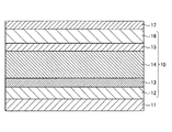
- FIG. 1 is a diagram schematically illustrating a configuration example of a photoelectric conversion element.
- FIG. 2 is a diagram schematically illustrating a configuration example of the image detection unit.
- FIG. 3 is a diagram schematically illustrating a configuration example of the fingerprint detection unit.
- Photoelectric conversion element The photoelectric conversion element of this embodiment includes an anode, a cathode, an active layer provided between the anode and the cathode, and at least one electron transport layer provided between the active layer and the cathode. At least one of the electron transport layers includes an insulating material and a semiconductor material, and the work function (Wf1) and the work function (Wf2) of the cathode satisfy the following expression. Wf2-Wf1 ⁇ 0.88 eV
- FIG. 1 is a diagram schematically illustrating a configuration example of the photoelectric conversion element of the present embodiment.
- the photoelectric conversion element 10 of the present embodiment is provided on, for example, a support substrate 11.
- the photoelectric conversion element 10 includes a cathode 12 provided in contact with the support substrate 11, an electron transport layer 13 provided in contact with the cathode 12, and an active layer provided in contact with the electron transport layer 13. It has a layer 14, a hole transport layer 15 provided in contact with the active layer 14, and an anode 16 provided in contact with the hole transport layer 15.
- a sealing substrate 17 provided so as to be in contact with the anode 16 is further provided.
- the photoelectric conversion element is usually formed on a substrate.
- an electrode including a cathode and an anode is formed on the substrate.
- the material of the substrate is not particularly limited as long as the material does not chemically change when a layer containing an organic compound is formed. Examples of the material of the substrate include glass, plastic, a polymer film, and silicon.
- the electrode on the opposite side to the electrode provided on the opaque substrate side is preferably a transparent or translucent electrode.
- a substrate on which an electrode (cathode or anode) described later or a layer structure on which an electrode can be formed by a further step such as a patterning step may be used as the substrate.
- the material of the transparent or translucent electrode examples include a conductive metal oxide film and a translucent metal thin film.
- conductive materials such as indium oxide, zinc oxide, tin oxide, and a complex thereof, such as indium tin oxide (ITO), indium zinc oxide (IZO), and NESA, gold, platinum, silver, and copper are used.
- ITO indium tin oxide
- IZO indium zinc oxide
- NESA gold, platinum, silver, and copper
- gold, platinum, silver, and copper are used.
- a transparent or translucent electrode a transparent conductive film in which an organic compound such as polyaniline and a derivative thereof and polythiophene and a derivative thereof are used may be used.
- the transparent or translucent electrode may be an anode or a cathode.
- the other electrode may be an electrode with low light transmittance.
- the material of the electrode having low light transmittance include a metal and a conductive polymer. Specific examples of the material of the electrode having low light transmittance include lithium, sodium, potassium, rubidium, cesium, magnesium, calcium, strontium, barium, aluminum, scandium, vanadium, zinc, yttrium, indium, cerium, samarium, europium, Metals such as terbium and ytterbium, and alloys of two or more thereof, or one or more of these metals, and gold, silver, platinum, copper, manganese, titanium, cobalt, nickel, tungsten, and tin Alloys with one or more metals selected from the group consisting of: graphite, graphite intercalation compounds, polyaniline and its derivatives, and polythiophene and its derivatives.
- Alloys include magnesium-silver alloys, magnesium-indium alloys, magnesium-aluminum alloys, indium-silver alloys, lithium-aluminum alloys, lithium-magnesium alloys, lithium-indium alloys, and calcium-aluminum alloys.
- the work function (Wf1) of the electron transport layer and the work function (Wf2) of the cathode satisfy the following expression (1).
- the material of the cathode can be selected in consideration of the work function of the cathode and the work function of the electron transport layer.
- Examples of the cathode material according to the present embodiment include ITO (work function: 5.1 eV), Au (work function: 5.2 eV), and Ag (work function: 4.9 eV).
- ITO is preferable from the viewpoint of light transmittance.
- the work function (Wf1) of the electron transport layer and the work function (Wf2) of the cathode satisfy the following equation (1-1) from the viewpoint of reducing the fluctuation of dark current due to the fluctuation of the voltage applied to the photoelectric conversion element. It is more preferable that the following formula (1-2) is satisfied, and it is more preferable that the following formula (1-3) is satisfied.
- the work function (Wf1) of the electron transport layer and the work function (Wf2) of the cathode preferably satisfy the following expression (1-4), and more preferably satisfy the following expression (1-5).
- the work function of the cathode can be measured using, for example, a Kelvin probe device (eg, FAC-2, manufactured by Riken Keiki Co., Ltd.).
- a Kelvin probe device eg, FAC-2, manufactured by Riken Keiki Co., Ltd.
- any conventionally known suitable method can be used.
- the method for forming the electrode include a vacuum deposition method, a sputtering method, an ion plating method, and a plating method.
- the method for forming an electrode may include further steps such as a step of patterning a layer formed by the above method and a step of performing a surface treatment.
- the photoelectric conversion element includes a charge transport layer (an electron transport layer, a hole transport layer, an electron injection layer) as a further component for improving characteristics such as an improvement in photoelectric conversion efficiency and a reduction in dark current.
- a charge transport layer an electron transport layer, a hole transport layer, an electron injection layer
- Layer hole injection layer
- any conventionally known arbitrary suitable material can be used.
- the material of the intermediate layer include halides and oxides of alkali metals or alkaline earth metals such as lithium fluoride.
- Examples of the material used for the intermediate layer include fine particles of an inorganic semiconductor material such as titanium oxide, and PEDOT (poly (3,4-ethylenedioxythiophene)) and PSS (poly (4-styrenesulfonate)). (PEDOT: PSS).
- the photoelectric conversion element may include a hole transport layer between the anode and the active layer.
- the hole transport layer has a function of transporting holes from the active layer to the electrode.
- the hole transport layer may be a single layer or a laminate of two or more layers.
- the hole transport layer provided in contact with the anode may be particularly referred to as a hole injection layer.
- the hole transport layer (hole injection layer) provided in contact with the anode has a function of promoting injection of holes into the anode.
- the hole transport layer (hole injection layer) may be in contact with the active layer.
- the hole transport layer includes a hole transport material.
- the hole transporting material include polythiophene and derivatives thereof, aromatic amine compounds, polymer compounds containing a structural unit having an aromatic amine residue, CuSCN, CuI, NiO, and molybdenum oxide (MoO 3 ).
- the hole transporting material include polythiophene and derivatives thereof, aromatic amine compounds, polymer compounds containing a structural unit having an aromatic amine residue, CuSCN, CuI, NiO, and molybdenum oxide (MoO 3 ).
- the photoelectric conversion element of the present embodiment may include an electron transport layer between the cathode and the active layer.
- the electron transport layer has a function of transporting electrons from the active layer to the cathode.
- the electron transport layer may be in contact with the cathode.
- the electron transport layer may be in contact with the active layer.
- the electron transport layer may be a single layer or a laminate of two or more layers. When there are two or more electron transport layers, at least one electron transport layer may be an electron transport layer that satisfies the requirements described above. Note that the electron transport layer provided in contact with the cathode may be particularly referred to as an electron injection layer.
- the electron transport layer of the present embodiment includes an insulating material and a semiconductor material.
- a specific description will be given.
- Insulating Material The work function (Wf3) of the insulating material, the work function (Wf1) of the electron transport layer, and the work function (Wf4) of the semiconductor material of the present embodiment are represented by the following expressions (3) and (3). 4) may be satisfied. Wf3> Wf1 (3) Wf3 ⁇ Wf4 (4) Insulating materials and semiconductor materials that may be included in the electron transport layer may be selected to satisfy such requirements.
- Examples of the insulating material that can be included in the electron transport layer of the present embodiment include compounds having an alkylene structure, polyvinylpyrrolidone (PVP), polymethyl methacrylate resin (PMMA), and poly (4-vinylphenol) (P-4VP). ).
- PVP polyvinylpyrrolidone
- PMMA polymethyl methacrylate resin
- P-4VP poly (4-vinylphenol
- the insulating material is preferably a polymer having an amino group or an alkoxy group.
- Examples of the compound having an alkylene structure include polyalkylenimine and derivatives thereof.
- Examples of polyalkyleneimines and derivatives thereof include alkyleneimines having 2 to 8 carbon atoms, such as ethyleneimine, propyleneimine, butyleneimine, dimethylethyleneimine, pentyleneimine, hexyleneimine, heptyleneimine, and octyleneimine, particularly Polymers obtained by polymerizing one or two or more of the alkylene imines of 2 to 4 by a conventional method, and polymers obtained by reacting them with various compounds and chemically modifying them are exemplified.
- polyalkyleneimine and its derivatives can effectively increase the work function of the electron transport layer, it contains polyethyleneimine (PEI) and polyalkyleneimine as a main chain, and ethylene oxide is added to a nitrogen atom in the main chain. It is preferable to use an ethoxylated polyethyleneimine (PEIE, work function: 4.1 eV) which is a modified product.
- PEIE polyethyleneimine
- PEIE work function: 4.1 eV
- semiconductor materials examples include metal compounds and metalloids.
- metal compounds include metal oxides, metal hydroxides and metal alkoxides.
- the metal oxide preferably contains a divalent or higher valent metal, and more preferably contains zinc or titanium.
- metal oxides examples include zinc oxide (ZnO, work function: 4.5 eV), aluminum-doped zinc oxide (AZO), gallium-doped zinc oxide (GZO), titanium oxide, and niobium oxide.
- ZnO zinc oxide
- AZO aluminum-doped zinc oxide
- GZO gallium-doped zinc oxide
- titanium oxide titanium oxide
- niobium oxide niobium oxide.
- a metal oxide containing zinc is preferable, and from the viewpoint of availability and processability, one or more oxide semiconductor materials selected from the group consisting of ZnO, AZO, and GZO are more preferable.
- metal hydroxide examples include zinc hydroxide, titanium hydroxide and niobium hydroxide.
- metal hydroxide a metal hydroxide containing zinc or titanium is preferable, and among them, titanium hydroxide is preferable.
- metal alkoxides examples include metal methoxide, metal ethoxide, metal propoxide, metal isopropoxide, metal n-butoxide, metal sec-butoxide, metal isobutoxide, and metal tert-butoxide.
- Metal alkoxides containing titanium are preferred, and titanium (IV) isopropoxide is particularly preferred.
- semimetals examples include Si, Ge, As, Sb and Te.
- the semiconductor material that can be included in the electron transport layer of the present embodiment is preferably, for example, nanoparticles having a particle size of 0.1 nm to 100 nm from the viewpoint of improving the characteristics of the photoelectric conversion element and making the production easier. .
- the intermediate layer is preferably formed by a coating method such as a slit coating method, a knife coating method, a spin coating method, a microgravure coating method, a gravure coating method, a bar coating method, and an inkjet printing method.
- a coating method such as a slit coating method, a knife coating method, a spin coating method, a microgravure coating method, a gravure coating method, a bar coating method, and an inkjet printing method.
- the photoelectric conversion device of the present embodiment is an organic photoelectric conversion device having at least one active layer containing an organic material.
- the active layer includes an organic material, and the organic material includes a polymer compound.
- the active layer of the present embodiment preferably has a bulk heterojunction structure including a p-type semiconductor material (electron donating compound) and an n-type semiconductor material (electron accepting compound).
- the work function (Wf1) of the electron transport layer and the energy level (LUMO) of the LUMO of the n-type semiconductor material included in the active layer satisfy the following expression (2-1). More preferably satisfy the following formula (2-2), and further preferably satisfy the following formula (2-3).
- ” means the absolute value of LUMO.
- the work function (Wf1) of the electron transport layer and the LUMO energy level (LUMO) of the n-type semiconductor material contained in the active layer preferably satisfy the following expression (2-4). It is more preferable to satisfy 5).
- the preferred p-type semiconductor material and n-type semiconductor material will be described later, but which of the p-type semiconductor material and the n-type semiconductor material depends on the selected p-type semiconductor material and n-type semiconductor material. It can be relatively determined from the energy level of HOMO or LUMO.
- the measurement of the HOMO and LUMO energy levels of the semiconductor material (p-type semiconductor material and n-type semiconductor material) of the present embodiment can be performed using a conventionally known measuring device according to a method known from literatures and the like. . Specifically, the measurement can be performed using a cyclic voltammetry measurement device (for example, Electrochemical Analyzer Model 600B, manufactured by BAS).
- a cyclic voltammetry measurement device for example, Electrochemical Analyzer Model 600B, manufactured by BAS.
- the thickness of the active layer is usually 1 nm to 100 ⁇ m.
- the thickness of the active layer of the photoelectric conversion element used as a light detection element is preferably from 500 nm to 1000 nm.
- the dark current ratio can be further reduced by having the configuration described above.
- the dark current ratio can be measured using any conventionally known and suitable measuring device.
- An example of the measuring device is a semiconductor parameter analyzer (B1500A, manufactured by Agilent Technologies).
- the dark current ratio is a ratio of a dark current obtained when a higher voltage is applied to a photoelectric conversion element to a dark current obtained when a lower voltage is applied (dark current ( (When high voltage is applied) / dark current (when low voltage is applied).
- the method for manufacturing the photoelectric conversion element of the present embodiment is not particularly limited.
- the photoelectric conversion element can be manufactured by a formation method suitable for a material selected in forming each component.
- the method for manufacturing a photoelectric conversion element includes an anode, a cathode, an active layer provided between the anode and the cathode, and at least one electron transport layer provided between the active layer and the cathode.
- One of the at least one electron transport layer includes an insulating material and a semiconductor material, and the work function (Wf1) of the one layer and the work function (Wf2) of the cathode are expressed by the following formula (1).
- a method for producing a photoelectric conversion element that satisfies the following, wherein a coating liquid containing an insulating material, a semiconductor material, and a solvent having a boiling point of 68 ° C. or higher is applied to form a coating film, and the coating film is dried. Curing to form an electron transport layer. Wf2-Wf1 ⁇ 0.88 eV (1)
- the electron transport layer of the present embodiment can be formed by a coating method using a coating liquid for forming an electron transport layer (hereinafter, sometimes referred to as ink). Note that other intermediate layers such as a hole transport layer can be formed in a similar manner.
- Step (i) is a step of forming a coating film by applying a coating liquid containing an insulating material, a semiconductor material, and a solvent having a boiling point of 68 ° C. or higher.
- the target to which the coating liquid for forming the electron transport layer is applied varies depending on the layer configuration and the order of layer formation of the photoelectric conversion element to be manufactured.
- the electron transport layer The application target of the coating liquid for formation is a cathode, a substrate on which the cathode is formed, or another electron transport layer.
- the application target of the coating liquid for forming an electron transport layer is an active layer or another electron transport layer.
- any suitable coating method can be used.
- a slit coating method, a knife coating method, a spin coating method, a microgravure coating method, a gravure coating method, a bar coating method, an inkjet printing method, a nozzle coating method, or a capillary coating method is preferable, and a spin coating method, a capillary coating method is preferable.
- a coating method or a bar coating method is more preferable, and a spin coating method is more preferable.
- the coating liquid for forming an electron transport layer may be a solution or a dispersion such as a dispersion, an emulsion (emulsion), or a suspension (suspension).
- the coating liquid for forming an electron transport layer may contain only one kind of solvent or may be a mixed solvent containing two or more kinds of solvents.
- Examples of the solvent having a boiling point of 68 ° C. or higher that may be contained in the electron transport layer coating liquid include water, alcohol, ketone, and hydrocarbon.
- alcohol examples include ethanol, 1-propanol, 2-propanol, 2-butanol, 2-pentanol, 3-pentanol, ethylene glycol, propylene glycol, butoxyethanol and methoxybutanol.
- ketones include acetone, methyl ethyl ketone, methyl isobutyl ketone, 2-heptanone, and cyclohexanone.
- hydrocarbon examples include n-pentane, cyclohexane, n-hexane, benzene, toluene, xylene, tetralin, chlorobenzene, and orthodichlorobenzene.
- the solvent preferably contains an alcohol solvent having a pKa (-logKa, where Ka is an acid dissociation constant) of 15.5 or more.
- alcohol solvents examples include alcohol solvents having 2 or more carbon atoms, and more specifically, ethanol (boiling point: 78.4 ° C., pKa: 15.9), 2-propanol (boiling point: 82 6.6 ° C, pKa: 16.5) and 3-pentanol (boiling point: 116 ° C, pKa: 18.2). That is, the coating liquid for forming an electron transport layer preferably contains one or more alcohol solvents selected from the group consisting of ethanol, 2-propanol and 3-pentanol.
- the work function of the electron transport layer is assumed from the work function of the selected insulating material and semiconductor material, and the work function of the conventional electron transport layer having a two-layer structure of, for example, ZnO / PEIE. Can be larger than would be possible.
- the amount of the solvent in the coating liquid for forming an electron transport layer is preferably 1 to 10,000 weight, and more preferably 10 to 1,000 weight, when the weight of a material other than the solvent that the electron transport layer can contain is 1. Is more preferable.
- Step (ii) is a step of curing the coating film by drying to form an electron transport layer.
- Any suitable method can be used as a method of curing the applied film by drying treatment, in other words, a method of forming the electron transport layer by removing the solvent from the applied film and curing the applied film.
- the drying method include a direct heating method using a hot plate, a hot air drying method, an infrared heating drying method, a flash lamp annealing drying method, and a drying method under reduced pressure.
- the active layer of the present embodiment can be formed by a coating method using a coating liquid (ink) for forming an active layer, similarly to the step of forming the electron transport layer described above. Therefore, detailed descriptions of common terms and steps may be omitted.
- the active layer which is a main component of the photoelectric conversion element of the present embodiment, preferably has a bulk heterojunction structure. Therefore, an active layer having a bulk heterojunction structure can be formed by a coating method using a coating liquid containing a p-type semiconductor material, an n-type semiconductor material, and a solvent.
- the step of forming an active layer includes forming a coating film by applying a coating solution containing a p-type semiconductor material, an n-type semiconductor material, and a solvent, and drying the coating film. This is a step of forming an active layer by curing by processing.
- Step (i) is a step of forming a coating film by applying a coating liquid containing a p-type semiconductor material, an n-type semiconductor material, and a solvent.
- any of the suitable coating methods described above can be used.
- the application target of the active layer forming coating liquid varies depending on the layer configuration and the order of layer formation of the photoelectric conversion element to be manufactured. For example, when the photoelectric conversion element has a layer structure of substrate / anode / hole transport layer / active layer / electron transport layer / cathode, and has a reverse stacked structure formed from the cathode side, an active layer is formed.
- An application target of the application liquid for an application is an electron transport layer.
- the application target of the active layer forming coating liquid is the hole transport layer.
- Step (ii) is a step of curing the coating film by drying to form an active layer.
- any of the above-described suitable methods can be used.
- the step of forming the active layer may include other steps in addition to the steps (i) and (ii), provided that the objects and effects of the present invention are not impaired.
- the method for manufacturing a photoelectric conversion element may be a method for manufacturing a photoelectric conversion element including a plurality of active layers. In this case, step (i) and step (ii) may be repeated a plurality of times.
- the active layer forming coating solution that can be used may be a solution or a dispersion such as a dispersion, an emulsion, or a suspension.
- the coating liquid for forming an active layer includes a p-type semiconductor material, an n-type semiconductor material, and a first solvent, and may further include a second solvent as desired.
- components of the coating solution for forming an active layer of the present embodiment will be described.
- the “polymer compound” means a polymer having a molecular weight distribution and a polystyrene equivalent number average molecular weight of 1 ⁇ 10 3 or more and 1 ⁇ 10 8 or less. The total of the constituent units contained in the polymer compound is 100 mol%.
- “Structural unit” means a unit present at least one in a polymer compound.
- the “hydrogen atom” may be a light hydrogen atom or a deuterium atom.
- Halogen includes fluorine, chlorine, bromine and iodine.
- May have a substituent means that all hydrogen atoms constituting the compound or the group are unsubstituted, and that one or more hydrogen atoms are partially or wholly substituted by a substituent. Includes both embodiments.
- the “alkyl group” may be linear, branched, or cyclic.
- the number of carbon atoms of the linear alkyl group is usually 1 to 50, preferably 1 to 30, and more preferably 1 to 20, excluding the number of carbon atoms of the substituent.
- the number of carbon atoms of the branched or cyclic alkyl group is usually from 3 to 50, preferably from 3 to 30, more preferably from 4 to 20, excluding the number of carbon atoms of the substituent.
- the alkyl group may have a substituent.
- Specific examples of the alkyl group include methyl, ethyl, n-propyl, isopropyl, n-butyl, isobutyl, tert-butyl, n-pentyl, isoamyl, 2-ethylbutyl, n-butyl Hexyl group, cyclohexyl group, n-heptyl group, cyclohexylmethyl group, cyclohexylethyl group, n-octyl group, 2-ethylhexyl group, 3-n-propylheptyl group, adamantyl group, n-decyl group, 3,7-dimethyl Octyl group, 2-ethyloctyl group, 2-n-hexyl-decyl group, n-dodecyl group, tetradecyl group, hexadecyl
- alkyl group having a substituent examples include a trifluoromethyl group, a pentafluoroethyl group, a perfluorobutyl group, a perfluorohexyl group, a perfluorooctyl group, a 3-phenylpropyl group, and 3- (4-methylphenyl) A propyl group, a 3- (3,5-di-n-hexylphenyl) propyl group, and a 6-ethyloxyhexyl group.
- Aryl group means an atomic group obtained by removing one hydrogen atom directly bonded to a carbon atom constituting a ring from an aromatic hydrocarbon which may have a substituent.
- the aryl group may have a substituent.
- Specific examples of the aryl group include a phenyl group, a 1-naphthyl group, a 2-naphthyl group, a 1-anthracenyl group, a 2-anthracenyl group, a 9-anthracenyl group, a 1-pyrenyl group, a 2-pyrenyl group, and a 4-pyrenyl group.
- 2-fluorenyl group, 3-fluorenyl group, 4-fluorenyl group, 2-phenylphenyl group, 3-phenylphenyl group, 4-phenylphenyl group, and these groups are an alkyl group, an alkoxy group, an aryl group, a fluorine atom And groups further having a substituent.
- the “alkoxy group” may be linear, branched, or cyclic.
- the number of carbon atoms of the linear alkoxy group is usually 1 to 40, preferably 1 to 10, excluding the number of carbon atoms of the substituent.
- the number of carbon atoms of the branched or cyclic alkoxy group is usually from 3 to 40, preferably from 4 to 10, excluding the number of carbon atoms of the substituent.
- the alkoxy group may have a substituent.
- Specific examples of the alkoxy group include methoxy, ethoxy, n-propyloxy, isopropyloxy, n-butyloxy, isobutyloxy, tert-butyloxy, n-pentyloxy, n-hexyloxy, Examples thereof include a cyclohexyloxy group, an n-heptyloxy group, an n-octyloxy group, a 2-ethylhexyloxy group, an n-nonyloxy group, an n-decyloxy group, a 3,7-dimethyloctyloxy group, and a lauryloxy group.
- the number of carbon atoms of the “aryloxy group” is usually from 6 to 60, preferably from 6 to 48, excluding the number of carbon atoms of the substituent.
- the aryloxy group may have a substituent.
- the aryloxy group include a phenoxy group, a 1-naphthyloxy group, a 2-naphthyloxy group, a 1-anthracenyloxy group, a 9-anthracenyloxy group, a 1-pyrenyloxy group, and these groups.
- examples thereof include groups further having a substituent such as an alkyl group, an alkoxy group, and a fluorine atom.
- alkylthio group may be linear, branched, or cyclic.
- the number of carbon atoms of the linear alkylthio group is usually 1 to 40, preferably 1 to 10, excluding the number of carbon atoms of the substituent.
- the number of carbon atoms of the branched and cyclic alkylthio groups is usually 3 to 40, preferably 4 to 10, excluding the number of carbon atoms of the substituent.
- the alkylthio group may have a substituent.
- Specific examples of the alkylthio group include methylthio, ethylthio, propylthio, isopropylthio, butylthio, isobutylthio, tert-butylthio, pentylthio, hexylthio, cyclohexylthio, heptylthio, octylthio, -Ethylhexylthio, nonylthio, decylthio, 3,7-dimethyloctylthio, laurylthio, and trifluoromethylthio.
- the number of carbon atoms of the “arylthio group” is usually from 6 to 60, preferably from 6 to 48, not including the number of carbon atoms of the substituent.
- the arylthio group may have a substituent.
- the arylthio group include a phenylthio group and a C1 to C12 alkyloxyphenylthio group (the description "C1 to C12" indicates that the group described immediately thereafter has 1 to 12 carbon atoms. The same applies to the following. ), C1-C12 alkylphenylthio, 1-naphthylthio, 2-naphthylthio, and pentafluorophenylthio.
- P-valent heterocyclic group (P represents an integer of 1 or more) means that a heterocyclic compound which may have a substituent is directly bonded to a carbon atom or a hetero atom constituting a ring. Means the remaining atomic groups excluding P hydrogen atoms among the hydrogen atoms. Among the P-valent heterocyclic groups, a “P-valent aromatic heterocyclic group” is preferable. “P-valent aromatic heterocyclic group” refers to an aromatic heterocyclic compound which may have a substituent, P atoms of a hydrogen atom directly bonded to a carbon atom or a hetero atom constituting a ring. Means the remaining atomic groups except for the hydrogen atom.
- Examples of the substituent which the heterocyclic compound may have include, for example, a halogen atom, an alkyl group, an aryl group, an alkoxy group, an aryloxy group, an alkylthio group, an arylthio group, a monovalent heterocyclic group, a substituted amino group , An acyl group, an imine residue, an amide group, an acid imide group, a substituted oxycarbonyl group, an alkenyl group, an alkynyl group, a cyano group, and a nitro group.
- the aromatic heterocyclic compound includes, in addition to the compound in which the heterocycle itself exhibits aromaticity, a compound in which an aromatic ring is further condensed with a heterocycle which does not exhibit aromaticity.
- aromatic heterocyclic compounds specific examples of the compound in which the heterocycle itself exhibits aromaticity include oxadiazole, thiadiazole, thiazole, oxazole, thiophene, pyrrole, phosphor, furan, pyridine, pyrazine, pyrimidine, and triazine. , Pyridazine, quinoline, isoquinoline, carbazole, and dibenzophosphole.
- aromatic heterocyclic compounds specific examples of the compound in which an aromatic ring is condensed to a heterocyclic ring that does not exhibit aromaticity include phenoxazine, phenothiazine, dibenzoborole, dibenzosilole, and benzopyran. .
- the number of carbon atoms of the monovalent heterocyclic group is usually 2 to 60, preferably 4 to 20, excluding the number of carbon atoms of the substituent.
- the monovalent heterocyclic group may have a substituent.
- Specific examples of the monovalent heterocyclic group include a thienyl group, a pyrrolyl group, a furyl group, a pyridyl group, a piperidyl group, a quinolyl group, an isoquinolyl group, a pyrimidinyl group, a triazinyl group, and a group in which these groups are an alkyl group, an alkoxy group, or the like. And a group having a substituent.
- Substituted amino group means an amino group having a substituent.
- substituent that the substituted amino group may have include an alkyl group, an aryl group, and a monovalent heterocyclic group.
- an alkyl group, an aryl group, or a monovalent heterocyclic group is preferable.
- the substituted amino group usually has 2 to 30 carbon atoms.
- substituted amino group examples include a dialkylamino group such as a dimethylamino group and a diethylamino group; a diphenylamino group; a bis (4-methylphenyl) amino group; a bis (4-tert-butylphenyl) amino group; And a diarylamino group such as a 5-di-tert-butylphenyl) amino group.
- the “acyl group” usually has 2 to 20 carbon atoms, and preferably 2 to 18 carbon atoms. Specific examples of the acyl group include an acetyl group, a propionyl group, a butyryl group, an isobutyryl group, a pivaloyl group, a benzoyl group, a trifluoroacetyl group, and a pentafluorobenzoyl group.
- Imine residue means an atomic group obtained by removing one hydrogen atom directly bonded to a carbon atom or a nitrogen atom constituting a carbon atom-nitrogen atom double bond from an imine compound.
- Imine compound means an organic compound having a carbon-nitrogen atom double bond in the molecule. Examples of the imine compound include aldimine, ketimine, and compounds in which a hydrogen atom bonded to a nitrogen atom constituting a carbon-nitrogen double bond in the aldimine is substituted with an alkyl group or the like.
- the diimine residue usually has about 2 to 20 carbon atoms, and preferably 2 to 18 carbon atoms.
- Examples of the imine residue include a group represented by the following formula.
- “Amido group” refers to the remaining atomic group obtained by removing one hydrogen atom bonded to a nitrogen atom from an amide.
- the number of carbon atoms of the amide group is usually 1-20, preferably 1-18.
- Specific examples of the amide group include a formamide group, an acetamido group, a propioamide group, a butyramide group, a benzamide group, a trifluoroacetamido group, a pentafluorobenzamide group, a diformamide group, a diacetamide group, a dipropioamide group, a dibutyramide group, and a dibenzamide group. , A ditrifluoroacetamide group, and a dipentafluorobenzamide group.
- Acid imide group means an atomic group obtained by removing one hydrogen atom bonded to a nitrogen atom from an acid imide.
- the acid imide group usually has 4 to 20 carbon atoms.
- Specific examples of the acid imide group include groups represented by the following formula.
- R ′ represents an alkyl group, an arylalkyl group, or a monovalent heterocyclic group.
- the number of carbon atoms of the substituted oxycarbonyl group is usually 2 to 60, preferably 2 to 48.
- substituted oxycarbonyl group examples include a methoxycarbonyl group, an ethoxycarbonyl group, a propoxycarbonyl group, an isopropoxycarbonyl group, a butoxycarbonyl group, an isobutoxycarbonyl group, a tert-butoxycarbonyl group, a pentyloxycarbonyl group, and a hexyloxycarbonyl group.
- alkenyl group may be linear, branched, or cyclic.
- the number of carbon atoms of the linear alkenyl group is usually from 2 to 30, preferably from 3 to 20, excluding the number of carbon atoms of the substituent.
- the number of carbon atoms of the branched or cyclic alkenyl group is usually 3 to 30, preferably 4 to 20, excluding the number of carbon atoms of the substituent.
- the alkenyl group may have a substituent.
- Specific examples of the alkenyl group include a vinyl group, a 1-propenyl group, a 2-propenyl group, a 2-butenyl group, a 3-butenyl group, a 3-pentenyl group, a 4-pentenyl group, a 1-hexenyl group, and a 5-hexenyl group. , 7-octenyl group, and groups in which these groups further have a substituent such as an alkyl group or an alkoxy group.
- the “alkynyl group” may be linear, branched, or cyclic.
- the number of carbon atoms of the linear alkenyl group is usually 2 to 20, preferably 3 to 20, excluding the number of carbon atoms of the substituent.
- the number of carbon atoms of the branched or cyclic alkenyl group is usually 4 to 30, preferably 4 to 20, excluding the number of carbon atoms of the substituent.
- the alkynyl group may have a substituent.
- Specific examples of the alkynyl group include an ethynyl group, a 1-propynyl group, a 2-propynyl group, a 2-butynyl group, a 3-butynyl group, a 3-pentynyl group, a 4-pentynyl group, a 1-hexynyl group, and a 5-hexynyl group.
- groups in which these groups further have a substituent such as an alkyl group or an alkoxy group.
- the p-type semiconductor material that can be included in the active layer of the photoelectric conversion element of the present embodiment is preferably a polymer compound having a predetermined polystyrene equivalent weight average molecular weight.
- the weight average molecular weight in terms of polystyrene means a weight average molecular weight calculated using gel permeation chromatography (GPC) and using a standard sample of polystyrene.
- the weight average molecular weight in terms of polystyrene of the p-type semiconductor material which is a polymer compound is preferably from 40,000 to 200,000, more preferably from 40,000 to 150,000, particularly from the viewpoint of reducing the dark current ratio. From the viewpoint of improving the solubility in a solvent, it is more preferably from 45,000 to 150,000.
- Examples of the p-type semiconductor material of the present embodiment include polyvinyl carbazole and its derivatives, polysilane and its derivatives, polysiloxane derivatives containing an aromatic amine structure in a side chain or a main chain, polyaniline and its derivatives, polythiophene and its derivatives, Polypyrrole and its derivatives, polyphenylenevinylene and its derivatives, polythienylenevinylene and its derivatives, polyfluorene and its derivatives.
- the p-type semiconductor material is preferably a polymer compound containing a structural unit represented by the following formula (I) and / or a structural unit represented by the following formula (II).
- Z represents a group represented by any of the following formulas (Z-1) to (Z-7).
- Ar 1 and Ar 2 represent a trivalent aromatic heterocyclic group which may be the same or different.
- Ar 3 represents a divalent aromatic heterocyclic group.
- R represents a hydrogen atom, a halogen atom, an amino group, an alkyl group, an aryl group, an alkoxy group, an aryloxy group, an alkylthio group, an arylthio group, a monovalent heterocyclic ring
- R represents a group, substituted amino group, acyl group, imine residue, amide group, acid imide group, substituted oxycarbonyl group, alkenyl group, alkynyl group, cyano group, or nitro group.
- the structural unit represented by the formula (I) is preferably a structural unit represented by the following formula (I-1).
- Z represents the same meaning as described above.
- Z is preferably a group represented by any of formulas (Z-4) to (Z-7).
- Examples of the structural unit represented by the formula (I-1) include structural units represented by the following formulas (501) to (505).
- R In the above formulas (501) to (505), R has the same meaning as described above. When there are two Rs, the two Rs may be the same or different from each other.
- R represents the same meaning as described above.
- Two Rs may be the same or different from each other.
- the number of carbon atoms of the divalent aromatic heterocyclic group represented by Ar 3 is usually 2 to 60, preferably 4 to 60, and more preferably 4 to 20.
- the divalent aromatic heterocyclic group represented by Ar 3 may have a substituent.
- substituent which the divalent aromatic heterocyclic group represented by Ar 3 may have include a halogen atom, an amino group, an alkyl group, an aryl group, an alkoxy group, an aryloxy group, an alkylthio group, Examples include an arylthio group, a monovalent heterocyclic group, a substituted amino group, an acyl group, an imine residue, an amide group, an acid imide group, a substituted oxycarbonyl group, an alkenyl group, an alkynyl group, a cyano group, and a nitro group.
- Examples of the divalent aromatic heterocyclic group represented by Ar 3 include groups represented by the following formulas (101) to (185).
- R In the formulas (101) to (185), R has the same meaning as described above. When a plurality of Rs are present, the plurality of Rs may be the same or different from each other.
- X 1 and X 2 each independently represent an oxygen atom or a sulfur atom, and R has the same meaning as described above.
- the plurality of Rs may be the same or different from each other.
- X 1 and X 2 in the formulas (II-1) to (II-6) are each preferably a sulfur atom.
- the P-type semiconductor material is preferably a polymer compound containing a structural unit having a thiophene skeleton.
- the polymer compound that is a P-type semiconductor material may include two or more types of structural units of the formula (I), and may include two or more types of structural units of the formula (II).
- the polymer compound that is a P-type semiconductor material may include a structural unit represented by the following formula (III).
- Ar 4 represents an arylene group.
- the arylene group represented by Ar 4 means an atomic group obtained by removing two hydrogen atoms from an aromatic hydrocarbon which may have a substituent.
- the aromatic hydrocarbon includes a compound having a condensed ring, and a compound in which two or more selected from the group consisting of an independent benzene ring and a condensed ring are bonded directly or via a divalent group such as a vinylene group. .
- Examples of the substituent that the aromatic hydrocarbon may have include the same substituents as those exemplified as the substituent that the heterocyclic compound may have.
- the number of carbon atoms in the arylene group excluding the substituent is usually from 6 to 60, preferably from 6 to 20.
- the number of carbon atoms of the arylene group including the substituent is usually 6 to 100.
- arylene group examples include a phenylene group (for example, the following formulas 1 to 3), a naphthalene-diyl group (for example, the following formulas 4 to 13), an anthracene-diyl group (for example, the following formulas 14 to 19), Biphenyl-diyl group (for example, the following formulas 20 to 25), terphenyl-diyl group (for example, the following formulas 26 to 28), fused ring compound group (for example, the following formulas 29 to 35), fluorene-diyl group (Eg, the following formulas 36 to 38) and a benzofluorene-diyl group (eg, the following formulas 39 to 46).
- a phenylene group for example, the following formulas 1 to 3
- a naphthalene-diyl group for example, the following formulas 4 to 13
- an anthracene-diyl group for example, the following formulas 14
- R as a substituent has the same meaning as described above.
- a plurality of Rs may be the same or different from each other.
- the structural unit constituting the polymer compound as a p-type semiconductor material is selected from the structural unit represented by the formula (I), the structural unit represented by the formula (II), and the structural unit represented by the formula (III) It may be a structural unit in which two or more types of structural units are combined and connected.
- the polymer compound as the p-type semiconductor material contains the structural unit represented by the formula (I) and / or the structural unit represented by the formula (II), the structural unit represented by the formula (I) and the formula
- the total amount of the structural units represented by (II) is usually 20 to 100% by mole of all the structural units (100% by mole) contained in the polymer compound, and the charge transport property as a p-type semiconductor material is Since it can be improved, it is preferably 40 to 100 mol%, more preferably 50 to 100 mol%.
- polymer compound that is a p-type semiconductor material examples include polymer compounds represented by the following formulas P-1 to P-6.
- the active layer forming coating liquid of the present embodiment may include only one type of p-type semiconductor material, or may include two or more types in any combination in any ratio.
- the difference between the work function of the electron transport layer and the LUMO energy level of the n-type semiconductor material described above is 0.06 eV or more. It can be selected in consideration of the work function of the electron transport layer.
- the n-type semiconductor material may be a low molecular compound or a high molecular compound.
- n-type semiconductor material which is a low molecular compound examples include oxadiazole derivatives, anthraquinodimethane and its derivatives, benzoquinone and its derivatives, naphthoquinone and its derivatives, anthraquinone and its derivatives, tetracyanoanthraquinodimethane and its derivatives, fluorenone derivatives, diphenyldicyanoethylene and derivatives thereof, diphenoquinone derivatives, metal complexes of 8-hydroxyquinoline and derivatives thereof, fullerenes and derivatives thereof such as C 60 fullerene, and phenanthrene derivatives such as bathocuproine.
- n-type semiconductor material which is a polymer compound examples include polyvinyl carbazole and its derivatives, polysilane and its derivatives, polysiloxane derivatives having an aromatic amine structure in a side chain or a main chain, polyaniline and its derivatives, polythiophene and its derivatives , Polypyrrole and its derivatives, polyphenylenevinylene and its derivatives, polythienylenevinylene and its derivatives, polyquinoline and its derivatives, polyquinoxaline and its derivatives, and polyfluorene and its derivatives.
- the n-type semiconductor material is preferably at least one selected from fullerenes and fullerene derivatives, and more preferably fullerene derivatives.
- fullerene examples include C 84 fullerene.
- fullerene derivative examples include these fullerene derivatives.
- the fullerene derivative means a compound in which at least a part of fullerene is modified.
- Examples of the fullerene derivative include compounds represented by the following formulas (N-1) to (N-4).
- Ra represents an alkyl group, an aryl group, a monovalent heterocyclic group, or a group having an ester structure.
- a plurality of Ra may be the same or different from each other.
- R b represents an alkyl group or an aryl group. A plurality of Rb may be the same or different from each other.
- Examples of the group having an ester structure represented by Ra include a group represented by the following formula (19).
- u1 represents an integer of 1 to 6.
- u2 represents an integer of 0 to 6.
- R c represents an alkyl group, an aryl group, or a monovalent heterocyclic group.
- Examples of C 60 fullerene derivatives include the following compounds.
- Examples of the C70 fullerene derivative include the following compounds.
- fullerene derivative examples include [6,6] -phenyl-C61 butyric acid methyl ester (C60PCBM, [6,6] -Phenyl C61ributyric acid methyl ester), [6,6] -phenyl-C71 butyric acid methyl ester ( C70PCBM, [6,6] -Phenyl C71 butyric acid methyl ester, [6,6] -Phenyl-C85 butyric acid methyl ester (C84PCBM, [6,6] -Phenyl C85 butyric acid methyl ester), and [6,6].
- ] -Thienyl-C61 butyric acid methyl ester [6,6] -Thienyl ⁇ C61 ⁇ butyric ⁇ acid ⁇ methyl ⁇ ester).
- the active layer forming coating liquid of the present embodiment may contain only one type of n-type semiconductor material, or may contain two or more types in any combination in any ratio.
- the solvent may be selected in consideration of solubility in the selected p-type semiconductor material and n-type semiconductor material and characteristics (eg, boiling point) for coping with drying conditions when forming the active layer.
- the first solvent which is the main solvent (good solvent), is an aromatic hydrocarbon (hereinafter simply referred to as an aromatic hydrocarbon) which may have a substituent (eg, an alkyl group or a halogen atom).
- the first solvent is preferably selected in consideration of the solubility of the selected p-type semiconductor material and n-type semiconductor material.
- aromatic hydrocarbons examples include toluene, xylene (eg, o-xylene, m-xylene, p-xylene), trimethylbenzene (eg, mesitylene, 1,2,4-trimethylbenzene (pseudocumene)) Butylbenzene (eg, n-butylbenzene, sec-butylbenzene, tert-butylbenzene), methylnaphthalene (eg, 1-methylnaphthalene), tetralin, indane, chlorobenzene, and dichlorobenzene (o-dichlorobenzene). .
- xylene eg, o-xylene, m-xylene, p-xylene
- trimethylbenzene eg, mesitylene, 1,2,4-trimethylbenzene (pseudocumene)
- Butylbenzene eg, n-butylbenz
- the first solvent may be composed of only one type of aromatic hydrocarbon, or may be composed of two or more types of aromatic hydrocarbons.
- the first solvent is preferably composed of only one kind of aromatic hydrocarbon.
- the first solvent is preferably toluene, o-xylene, m-xylene, p-xylene, mesitylene, pseudocumene, n-butylbenzene, sec-butylbenzene, tert-butylbenzene, methylnaphthalene, tetralin, indane, chlorobenzene and It contains one or more selected from the group consisting of o-dichlorobenzene, and more preferably contains o-xylene, pseudocumene, tetralin, chlorobenzene or o-dichlorobenzene.
- the second solvent is a solvent selected particularly from the viewpoint of increasing the solubility of the n-type semiconductor material.
- the second solvent include ketone solvents such as acetone, methyl ethyl ketone, cyclohexanone, acetophenone and propiophenone, ethyl acetate, butyl acetate, phenyl acetate, ethyl cellosolve acetate, methyl benzoate, butyl benzoate, benzyl benzoate and the like. Ester solvents.
- the second solvent is preferably acetophenone, propiophenone, or benzyl benzoate.
- the weight ratio of the first solvent to the second solvent is in the range of 85/15 to 97/3 from the viewpoint of further improving the solubility of the p-type semiconductor material and the n-type semiconductor material. Is preferred.
- the total weight of the first solvent and the second solvent contained in the active layer forming coating liquid of the present embodiment is such that the total weight of the active layer forming coating liquid is 100% by weight, and the p-type semiconductor material and the n-type From the viewpoint of further improving the solubility of the semiconductor material, it is preferably 90% by weight or more, more preferably 92% by weight or more, and still more preferably 95% by weight or more. From the viewpoint of easily forming a layer having a certain thickness or more by increasing the concentration of the n-type semiconductor material, preferably 99% by weight or less, more preferably 98% by weight or less, and still more preferably 97.5% by weight or less. It is.
- the coating solution for forming an active layer according to the present embodiment may contain any solvent other than the first solvent and the second solvent.
- the content of any solvent is preferably 5% by weight or less, more preferably 3% by weight or less, More preferably, it is 1% by weight or less.
- the optional solvent a solvent having a higher boiling point than the second solvent is preferable.
- the coating solution for forming an active layer according to the present embodiment includes, in addition to the first solvent, the second solvent, the p-type semiconductor material, and the n-type semiconductor material, an ultraviolet absorbent as long as the object and effects of the present invention are not impaired.
- An optional component such as an antioxidant, a sensitizer for sensitizing a function of generating charges by absorbed light, and a light stabilizer for increasing stability to ultraviolet rays may be contained.
- the total concentration of the p-type semiconductor material and the n-type semiconductor material in the active layer forming coating solution of the present embodiment is preferably 0.01% by weight or more and 20% by weight or less, and more preferably 0.01% by weight or more and 10% by weight or less. % By weight, more preferably from 0.01% by weight to 5% by weight, and particularly preferably from 0.1% by weight to 5% by weight.
- the p-type semiconductor material and the n-type semiconductor material may be dissolved or dispersed.
- the p-type semiconductor material and the n-type semiconductor material are preferably at least partially dissolved, and more preferably all are dissolved.
- the coating solution for forming an active layer of the present embodiment can be prepared by a known method. For example, a method of preparing a mixed solvent by mixing a first solvent and a second solvent, adding a p-type semiconductor material and an n-type semiconductor material to the obtained mixed solvent, and adding a p-type semiconductor material to the first solvent
- the second solvent can be prepared by adding the n-type semiconductor material to the second solvent, and then mixing the first solvent and the second solvent to which the respective materials have been added.
- the first solvent and the second solvent, and the p-type semiconductor material and the n-type semiconductor material may be heated and mixed at a temperature equal to or lower than the boiling point of the solvent.
- the obtained mixture may be filtered using a filter, and the obtained filtrate may be used as ink.
- a filter for example, a filter formed of a fluororesin such as polytetrafluoroethylene (PTFE) can be used.
- the photoelectric conversion element of this embodiment can generate a photoelectromotive force between the electrodes by being irradiated with light, and can operate as a solar cell. Further, a thin film solar cell module can be obtained by integrating a plurality of solar cells.
- the photoelectric conversion element of the present embodiment can flow a photocurrent by irradiating light from the transparent or translucent electrode side in a state where a voltage is applied between the electrodes. ).
- a plurality of optical sensors can be integrated to be used as an image sensor.
- the photoelectric conversion element according to the embodiment of the present invention described above is suitably applied to a detection unit provided in various electronic devices such as a workstation, a personal computer, a portable information terminal, an access control system, a digital camera, and a medical device. can do.
- the photoelectric conversion element (light detection element) of the present invention includes, for example, an image detection unit (image sensor) for a solid-state imaging device such as an X-ray imaging device and a CMOS image sensor, a fingerprint detection unit, and the like.
- image detection unit image sensor
- CMOS image sensor CMOS image sensor
- the present invention can be suitably applied to a detection unit that detects a predetermined feature of a part of a living body, such as a face detection unit, a vein detection unit, and an iris detection unit, and a detection unit of an optical biosensor such as a pulse oximeter.
- FIG. 2 is a diagram schematically illustrating a configuration example of an image detection unit for a solid-state imaging device.
- the image detection unit 1 includes a CMOS transistor substrate 20, an interlayer insulating film 30 provided so as to cover the CMOS transistor substrate 20, and a photoelectric conversion according to the embodiment of the present invention provided on the interlayer insulating film 30.
- the element 10 is provided so as to penetrate the interlayer insulating film 30, and is provided so as to cover the photoelectric conversion element 10, and an interlayer wiring part 32 for electrically connecting the CMOS transistor substrate 20 and the photoelectric conversion element 10.
- a color filter 50 provided on the sealing layer 40.
- the CMOS transistor substrate 20 has a conventionally known arbitrary suitable configuration in a form according to the design.
- the CMOS transistor substrate 20 includes functional elements such as a CMOS transistor circuit (MOS transistor circuit) for realizing various functions, including a transistor, a capacitor and the like formed within the thickness of the substrate.
- MOS transistor circuit CMOS transistor circuit
- the functional element includes, for example, a floating diffusion, a reset transistor, an output transistor, and a selection transistor.
- CMOS A signal readout circuit and the like are built in the CMOS transistor substrate 20 by using such functional elements and wirings.
- the interlayer insulating film 30 can be made of a conventionally known arbitrary suitable insulating material such as silicon oxide and insulating resin.
- the interlayer wiring portion 32 can be made of a conventionally known arbitrary suitable conductive material (wiring material) such as copper and tungsten.
- the interlayer wiring section 32 may be, for example, an in-hole wiring formed simultaneously with the formation of the wiring layer, or a buried plug formed separately from the wiring layer.
- the sealing layer 40 is made of a conventionally known arbitrary suitable material, provided that it can prevent or suppress penetration of harmful substances such as oxygen and water which may functionally deteriorate the photoelectric conversion element 10. Can be.
- the sealing layer 40 may be constituted by the sealing substrate 17 already described.
- the color filter 50 for example, a primary color filter that is made of a conventionally known arbitrary suitable material and that corresponds to the design of the image detection unit 1 can be used. Further, as the color filter 50, a complementary color filter whose thickness can be reduced as compared with the primary color filter can be used. As complementary color filters, for example, three types of (yellow, cyan, magenta), three types of (yellow, cyan, transparent), three types of (yellow, transparent, magenta), and three types of (transparent, cyan, magenta) Color filters in which types are combined can be used. These can have any suitable arrangement corresponding to the design of the photoelectric conversion element 10 and the CMOS transistor substrate 20, provided that color image data can be generated.
- the light received by the photoelectric conversion element 10 via the color filter 50 is converted by the photoelectric conversion element 10 into an electric signal corresponding to the amount of received light, and the light reception signal outside the photoelectric conversion element 10 via the electrode, that is, the imaging target Is output as an electric signal corresponding to.
- the light receiving signal output from the photoelectric conversion element 10 is input to the CMOS transistor substrate 20 via the interlayer wiring portion 32, and is read by a signal readout circuit built in the CMOS transistor substrate 20, and further not shown.
- image information based on an imaging target is generated.
- FIG. 3 is a diagram schematically illustrating a configuration example of a fingerprint detection unit integrally formed with the display device.
- the display device 2 of the portable information terminal includes a fingerprint detection unit 100 including the photoelectric conversion element 10 according to the embodiment of the present invention as a main component, and a display panel provided on the fingerprint detection unit 100 and displaying a predetermined image.
- a fingerprint detection unit 100 including the photoelectric conversion element 10 according to the embodiment of the present invention as a main component and a display panel provided on the fingerprint detection unit 100 and displaying a predetermined image.
- Unit 200 The display device 2 of the portable information terminal includes a fingerprint detection unit 100 including the photoelectric conversion element 10 according to the embodiment of the present invention as a main component, and a display panel provided on the fingerprint detection unit 100 and displaying a predetermined image.
- the fingerprint detection unit 100 is provided in an area that substantially matches the display area 200a of the display panel unit 200.
- the display panel unit 200 is integrally laminated above the fingerprint detection unit 100.
- the fingerprint detection unit 100 may be provided so as to correspond to only the part of the area.
- the fingerprint detection unit 100 includes the photoelectric conversion element 10 according to the embodiment of the present invention as a functional unit having an essential function.
- the fingerprint detection unit 100 may be any suitable conventionally known member such as a protection film (protection film), a support substrate, a sealing substrate, a sealing member, a barrier film, a bandpass filter, and an infrared cut film (not shown). It can be provided in a manner corresponding to a design that can obtain characteristics.
- the fingerprint detecting unit 100 may employ the configuration of the image detecting unit described above.
- the photoelectric conversion element 10 can be included in the display area 200a in any mode.
- a plurality of photoelectric conversion elements 10 may be arranged in a matrix.
- the photoelectric conversion element 10 is provided on the support substrate 11 or the sealing substrate, and the support substrate 11 is provided with electrodes (anode or cathode) in, for example, a matrix.
- the light received by the photoelectric conversion element 10 is converted by the photoelectric conversion element 10 into an electric signal corresponding to the amount of received light, and is received outside the photoelectric conversion element 10 via the electrode, that is, an electric signal corresponding to the fingerprint imaged. Output as a signal.
- the display panel section 200 is configured as an organic electroluminescence display panel (organic EL display panel) including a touch sensor panel in this configuration example.
- the display panel unit 200 may be configured by a display panel having any suitable conventionally known configuration such as a liquid crystal display panel including a light source such as a backlight, instead of the organic EL display panel, for example.
- the display panel unit 200 is provided on the fingerprint detection unit 100 described above.
- the display panel section 200 includes an organic electroluminescent element (organic EL element) 220 as a functional section having an essential function.
- the display panel unit 200 further includes a substrate (supporting substrate 210 or a sealing substrate 240) such as a glass substrate, and a sealing member, a barrier film, a polarizing plate such as a circularly polarizing plate, and a touch sensor panel 230.
- Suitable conventionally known members may be provided in a manner corresponding to desired characteristics.
- the organic EL element 220 is used as a light source for pixels in the display area 200a and also as a light source for capturing a fingerprint in the fingerprint detection unit 100.
- the fingerprint detection unit 100 detects a fingerprint using light emitted from the organic EL element 220 of the display panel unit 200. Specifically, the light radiated from the organic EL element 220 passes through a component existing between the organic EL element 220 and the photoelectric conversion element 10 of the fingerprint detection unit 100, and the light in the display area 200a is displayed. The light is reflected by the skin (finger surface) of the fingertip of the finger placed so as to be in contact with the surface of the panel section 200.
- At least a part of the light reflected by the finger surface is transmitted through the intervening components, received by the photoelectric conversion element 10, and converted into an electric signal corresponding to the amount of light received by the photoelectric conversion element 10. Then, image information about the fingerprint on the finger surface is formed from the converted electric signal.
- the portable information terminal provided with the display device 2 performs fingerprint authentication by comparing the obtained image information with fingerprint data for fingerprint authentication recorded in advance by any conventionally known and suitable steps.
- Example 1 Production and evaluation of photoelectric conversion element (production of photoelectric conversion element) An ITO thin film (cathode) was formed with a thickness of 150 nm on a glass substrate by a sputtering method. An ozone UV treatment was performed on the surface of the glass substrate.
- PEIE polyethylene imine ethoxylate
- % of a zinc oxide / isopropanol dispersion was mixed to prepare a coating liquid for forming an electron transport layer.
- the obtained coating liquid for forming an electron transport layer was applied by a spin coating method onto an ITO thin film on a glass substrate that had been subjected to an ozone UV treatment, thereby forming a coating film.
- the glass substrate on which the coating film was formed was subjected to a heat treatment at 120 ° C. for 10 minutes using a hot plate to cure the formed coating film, thereby forming an electron transport layer on the ITO thin film serving as a cathode. .
- the thickness of the obtained electron transport layer was 50 nm.
- Ratio (p / n ratio) between the weight of a polymer compound P-1 represented by the following formula, which is a p-type semiconductor material, and the weight of C60PCBM (manufactured by Frontier Carbon Co., trade name: E100) which is an n-type semiconductor material. was 1 / 1.75.
- the obtained coating solution for forming an active layer was applied on an electron transporting layer formed on a glass substrate by a spin coating method to form a coating film.
- An active layer was formed by subjecting the obtained coating film to a drying process of heating for 10 minutes using a hot plate heated to 100 ° C.
- the thickness of the obtained active layer was 550 nm.
- a hole transport layer was formed by depositing molybdenum oxide (MoO 3 ) to a thickness of about 30 nm on the obtained active layer using a resistance heating evaporation apparatus.
- MoO 3 molybdenum oxide
- a silver (Ag) layer was deposited to a thickness of about 80 nm on the obtained hole transport layer to form an anode, thereby producing a photoelectric conversion element (photodetection element).
- a photoelectric conversion element obtained by applying a UV curing agent on a sealing substrate (glass substrate) was attached so as to surround the UV curing agent, and then the photoelectric conversion element was sealed by irradiating UV light.
- the planar shape of the obtained photoelectric conversion element when viewed in the thickness direction was a square of 2 mm ⁇ 2 mm.
- the dark current ratio means a ratio of a dark current obtained when a voltage of 10 V is applied to a dark current obtained when a voltage of 2 V is applied (dark current (10 V) / dark current (2 V)). .
- the dark current was measured using a semiconductor parameter analyzer (B1500A, manufactured by Agilent Technologies) when a reverse bias voltage of 10 V or 2 V was applied. The dark current ratio was calculated based on the obtained dark current value.
- the CV measurement was performed under the same conditions as the method described in Advanced Materials, Volume 18, 2006, pp. 789-794.
- the equipment used was as follows.
- CV measurement device BAS, Electrochemical Analyzer Model 600B Supporting electrolyte: tetrabutylammonium hexafluorophosphate (TBAPF 6, Aldrich Co.) containing concentrations 0.1 M, dehydrated acetonitrile solution working electrode: (dropwise a solution prepared by dissolving in chloroform) platinum foil / n-type semiconductor material Counter electrode: Platinum foil Reference electrode: Ag / AgCl electrode Standard potential: Ferrocene
- the energy level of LUMO of C60PCBM was -4.3 eV.
- the coating liquid for forming an electron transport layer is applied to a glass substrate, and heated using a hot plate at 120 ° C. for 10 minutes to obtain an electron transport layer.
- As a Kelvin probe device FAC-2 manufactured by Riken Keiki Co., Ltd. was used.
- Gold (WF: 5.1 eV) was used as a reference sample for calibration.
- the work function of the electron transport layer was 3.77 eV.
- the work function of the cathode is obtained by forming an ITO thin film (cathode) with a thickness of 150 nm on a glass substrate and measuring the formed ITO thin film using a Kelvin probe device. I asked for it.
- a Kelvin probe device FAC-2 manufactured by Riken Keiki Co., Ltd. was used.
- Gold WF: 5.1 eV was used as a reference sample for calibration.
- the work function of the cathode was 4.80 eV.
- Example 2 A photoelectric conversion element was manufactured and evaluated in the same manner as in Example 1 except that 2-propanol was used instead of 3-pentanol used as a solvent in the coating liquid for forming an electron transport layer.
- Example 3 A photoelectric conversion element was manufactured and evaluated in the same manner as in Example 1 except that ethanol was used instead of 3-pentanol used as a solvent in the coating liquid for forming an electron transport layer.
- Electron prepared by mixing 0.1 g of a 1% by weight aqueous solution of polyethyleneimine ethoxylate (PEIE) (product name: polyethyleneimine, 80% ethoxylated solution, weight average molecular weight 110,000, manufactured by Aldrich) with 10 g of water.
- PEIE polyethyleneimine ethoxylate
- a photoelectric conversion element was manufactured and evaluated in the same manner as in Example 1 except that the coating solution for forming a transport layer was used.
- Example 2 Same as Example 1 except that a 10 wt% zinc oxide / isopropanol dispersion (manufactured by Teica, product name: HTD-711Z) was diluted 10-fold with 3-pentanol to form an electron transport layer-forming coating solution. Then, a photoelectric conversion element was manufactured and evaluated.
- a 10 wt% zinc oxide / isopropanol dispersion manufactured by Teica, product name: HTD-711Z
- HTD-711Z 3-pentanol
- the glass substrate coated with the first electron transport layer forming coating solution was heated at 120 ° C. for 10 minutes using a hot plate to form a first electron transport layer on the ITO thin film serving as a cathode.
- the electron transport layer of Comparative Example 3 has a two-layer structure in which the first electron transport layer and the second electron transport layer are stacked.
- ⁇ Wf which is the difference between the work function of the electron transport layer and the work function of the cathode
- ⁇ E which is the difference between the work function of the electron transport layer and the LUMO energy level of the n-type semiconductor material
- the photoelectric conversion element of the present invention has a small variation in dark current even when the applied voltage to the photoelectric conversion element is varied, so that the required operating voltage is different without any special design change or the like. It can be flexibly applied to various uses.
Landscapes
- Chemical & Material Sciences (AREA)
- Engineering & Computer Science (AREA)
- Materials Engineering (AREA)
- Physics & Mathematics (AREA)
- Electromagnetism (AREA)
- Nanotechnology (AREA)
- Photovoltaic Devices (AREA)
- Light Receiving Elements (AREA)
- Electroluminescent Light Sources (AREA)
- Solid State Image Pick-Up Elements (AREA)
- Inorganic Chemistry (AREA)
Abstract
暗電流比を低減する。 光電変換素子10は、陽極16と、陰極12と、該陽極及び陰極間に設けられている活性層14と、活性層及び陰極間に設けられている少なくとも1層の電子輸送層13とを含み、電子輸送層が、絶縁性材料と、半導体材料とを含み、電子輸送層の仕事関数と陰極の仕事関数との差が、0.88eV以上である。 さらに、前記活性層がp型半導体材料及びn型半導体材料を含み、 前記電子輸送層の仕事関数(Wf1)と前記n型半導体材料のLUMOのエネルギーレベル(LUMO)とが下記式(2)を満たす光電変換素子。 |LUMO|-Wf1≧0.06eV (2)
Description
本発明は、光電変換素子及びその製造方法に関する。
光電変換素子は、例えば、省エネルギー、二酸化炭素の排出量の低減の観点から極めて有用なデバイスであり、注目されている。
光電変換素子とは、陽極及び陰極からなる一対の電極と、該一対の電極間に設けられる活性層とを少なくとも備える素子である。光電変換素子では、いずれかの電極を透明または半透明の材料から構成し、透明または半透明とした電極側から活性層に光を入射させる。活性層に入射した光のエネルギー(hν)によって、活性層において電荷(正孔及び電子)が生成し、生成した正孔は陽極に向かって移動し、電子は陰極に向かって移動する。
そして、陽極及び陰極に到達した電荷は、素子の外部に取り出される。
そして、陽極及び陰極に到達した電荷は、素子の外部に取り出される。
光電変換素子は例えば光検出素子として用いられる。光検出素子として用いられる光電変換素子は、電圧が印加された状態で使用され、素子に入射した光が変換されて電流として検出される。しかしながら、光が入射していない状態であっても、光電変換素子に微弱な電流が流れる。この電流は暗電流として知られており、光検出の精度を低下させる要因となっているが、一般に、暗電流は光電変換素子に印加される電圧によって変動する。
光電変換素子に印加される電圧は当該素子が搭載されるデバイスの種類に応じて異なるため、暗電流は素子が搭載されるデバイスによって異なる。汎用性の観点からは、搭載されるデバイスに応じて暗電流が変動しない方が好ましい。
光電変換素子における光電変換効率などの特性の向上を目的として、酸化亜鉛とPFN(ポリ[(9,9-ビス(3’-(N,N-ジメチルアミノ)プロピル)-2,7-フルオレン)-alt-2,7-(9,9-ジオクチル)フルオレン])又はPEI(ポリエチレンイミン)とを含む単層の電子輸送層を用いる構成が知られている(非特許文献1及び2参照)。
Solar Energy Materials & Solar Cells 141 (2015) 248-259
Organic Electronics 38 (2016) 150-157
しかしながら、上記の非特許文献1及び2が開示する光電変換素子では、光電変換素子に印加される電圧の変動による暗電流の変動を低減させることは十分ではなかった。
本発明者らは、上記課題を解決すべく、鋭意研究を進めたところ、電子輸送層の仕事関数及び陰極の仕事関数が所定の関係を満たすようにすれば、光電変換素子に印加される電圧の変動による暗電流の変動を低減できることを見出し、本発明を完成するに至った。
すなわち、本発明は、下記[1]~[20]を提供する。
[1]陽極と、陰極と、該陽極及び陰極間に設けられている活性層と、該活性層及び前記陰極間に設けられている少なくとも1層の電子輸送層とを含み、
前記少なくとも1層の電子輸送層のうちの1層が、絶縁性材料と、半導体材料とを含み、当該1層の仕事関数(Wf1)と前記陰極の仕事関数(Wf2)とが下記式(1)を満たす光電変換素子。
Wf2-Wf1≧0.88eV (1)
[2]前記活性層がp型半導体材料及びn型半導体材料を含み、
前記電子輸送層の仕事関数(Wf1)と前記n型半導体材料のLUMOのエネルギーレベル(LUMO)とが下記式(2)を満たす[1]に記載の光電変換素子。
|LUMO|-Wf1≧0.06eV (2)
[3]前記n型半導体材料が、フラーレン誘導体である、[1]又は[2]に記載の光電変換素子。
[4]前記フラーレン誘導体が、C60PCBMである、[3]に記載の光電変換素子。
[5]前記絶縁性材料の仕事関数(Wf3)、前記電子輸送層の仕事関数(Wf1)及び前記半導体材料の仕事関数(Wf4)が下記式(3)及び下記式(4)を満たす、[1]~[4]のいずれか1つに記載の光電変換素子。
Wf3>Wf1 (3)
Wf3<Wf4 (4)
[6]前記半導体材料が、ZnO、AZO及びGZOからなる群から選択される1以上の酸化物半導体材料である、[1]~[5]のいずれか1つに記載の光電変換素子。
[7]前記絶縁性材料が、アミノ基又はアルコキシ基を有する重合体である、[1]~[6]のいずれか1つに記載の光電変換素子。
[8]前記絶縁性材料が、エトキシ化ポリエチレンイミンである、[7]に記載の光電変換素子。
[9]前記電子輸送層が、前記絶縁性材料と前記半導体材料と沸点が68℃以上である溶媒とを含む塗布膜を乾燥処理することにより硬化した層である、[1]~[8]のいずれか1つに記載の光電変換素子。
[10]前記溶媒が、pKaが15.5以上であるアルコール溶媒を含む、[9]に記載の光電変換素子。
[11]前記アルコール溶媒が、エタノール、2-プロパノール及び3-ペンタノールからなる群から選択される1以上のアルコール溶媒を含む、[10]に記載の光電変換素子。
[12]光検出素子である、[1]~[11]のいずれか1つに記載の光電変換素子。
[13][12]に記載の光電変換素子を含む、イメージセンサー。
[14][12]に記載の光電変換素子を含む、指紋認証装置。
[15][1]に記載の光電変換素子の製造方法において、
前記絶縁性材料と前記半導体材料と沸点が68℃以上である溶媒とを含む塗布液を塗布して塗布膜を形成し、該塗布膜を乾燥処理することにより硬化して前記電子輸送層を形成する工程を含む、光電変換素子の製造方法。
[16]前記半導体材料が、ZnO、AZO及びGZOからなる群から選択される1以上の酸化物半導体材料である、[15]に記載の光電変換素子の製造方法。
[17]前記絶縁性材料が、アミノ基又はアルコキシ基を有する重合体である、[15]又は[16]に記載の光電変換素子の製造方法。
[18]前記絶縁性材料が、エトキシ化ポリエチレンイミンである、[17]に記載の光電変換素子の製造方法。
[19]前記溶媒が、pKaが15.5以上であるアルコール溶媒を含む、[15]~[18]のいずれか1つに記載の光電変換素子の製造方法。
[20]前記アルコール溶媒が、エタノール、2-プロパノール及び3-ペンタノールからなる群から選択される1以上のアルコール溶媒を含む、[19]に記載の光電変換素子の製造方法。
[1]陽極と、陰極と、該陽極及び陰極間に設けられている活性層と、該活性層及び前記陰極間に設けられている少なくとも1層の電子輸送層とを含み、
前記少なくとも1層の電子輸送層のうちの1層が、絶縁性材料と、半導体材料とを含み、当該1層の仕事関数(Wf1)と前記陰極の仕事関数(Wf2)とが下記式(1)を満たす光電変換素子。
Wf2-Wf1≧0.88eV (1)
[2]前記活性層がp型半導体材料及びn型半導体材料を含み、
前記電子輸送層の仕事関数(Wf1)と前記n型半導体材料のLUMOのエネルギーレベル(LUMO)とが下記式(2)を満たす[1]に記載の光電変換素子。
|LUMO|-Wf1≧0.06eV (2)
[3]前記n型半導体材料が、フラーレン誘導体である、[1]又は[2]に記載の光電変換素子。
[4]前記フラーレン誘導体が、C60PCBMである、[3]に記載の光電変換素子。
[5]前記絶縁性材料の仕事関数(Wf3)、前記電子輸送層の仕事関数(Wf1)及び前記半導体材料の仕事関数(Wf4)が下記式(3)及び下記式(4)を満たす、[1]~[4]のいずれか1つに記載の光電変換素子。
Wf3>Wf1 (3)
Wf3<Wf4 (4)
[6]前記半導体材料が、ZnO、AZO及びGZOからなる群から選択される1以上の酸化物半導体材料である、[1]~[5]のいずれか1つに記載の光電変換素子。
[7]前記絶縁性材料が、アミノ基又はアルコキシ基を有する重合体である、[1]~[6]のいずれか1つに記載の光電変換素子。
[8]前記絶縁性材料が、エトキシ化ポリエチレンイミンである、[7]に記載の光電変換素子。
[9]前記電子輸送層が、前記絶縁性材料と前記半導体材料と沸点が68℃以上である溶媒とを含む塗布膜を乾燥処理することにより硬化した層である、[1]~[8]のいずれか1つに記載の光電変換素子。
[10]前記溶媒が、pKaが15.5以上であるアルコール溶媒を含む、[9]に記載の光電変換素子。
[11]前記アルコール溶媒が、エタノール、2-プロパノール及び3-ペンタノールからなる群から選択される1以上のアルコール溶媒を含む、[10]に記載の光電変換素子。
[12]光検出素子である、[1]~[11]のいずれか1つに記載の光電変換素子。
[13][12]に記載の光電変換素子を含む、イメージセンサー。
[14][12]に記載の光電変換素子を含む、指紋認証装置。
[15][1]に記載の光電変換素子の製造方法において、
前記絶縁性材料と前記半導体材料と沸点が68℃以上である溶媒とを含む塗布液を塗布して塗布膜を形成し、該塗布膜を乾燥処理することにより硬化して前記電子輸送層を形成する工程を含む、光電変換素子の製造方法。
[16]前記半導体材料が、ZnO、AZO及びGZOからなる群から選択される1以上の酸化物半導体材料である、[15]に記載の光電変換素子の製造方法。
[17]前記絶縁性材料が、アミノ基又はアルコキシ基を有する重合体である、[15]又は[16]に記載の光電変換素子の製造方法。
[18]前記絶縁性材料が、エトキシ化ポリエチレンイミンである、[17]に記載の光電変換素子の製造方法。
[19]前記溶媒が、pKaが15.5以上であるアルコール溶媒を含む、[15]~[18]のいずれか1つに記載の光電変換素子の製造方法。
[20]前記アルコール溶媒が、エタノール、2-プロパノール及び3-ペンタノールからなる群から選択される1以上のアルコール溶媒を含む、[19]に記載の光電変換素子の製造方法。
本発明にかかる光電変換素子によれば、光電変換素子に印加される電圧の変動による暗電流の変動を低減することができる。
以下、図面を参照して、本発明の実施形態にかかる光電変換素子について説明する。なお、図面は、発明が理解できる程度に、構成要素の形状、大きさ及び配置が概略的に示されているに過ぎない。本発明は以下の記述によって限定されるものではなく、各構成要素は本発明の要旨を逸脱しない範囲において適宜変更可能である。また、本発明の実施形態にかかる構成は、必ずしも図面に示された配置で、製造されたり、使用されたりするとは限らない。
1.光電変換素子
本実施形態の光電変換素子は、陽極と、陰極と、陽極及び陰極間に設けられている活性層と、活性層及び陰極間に設けられている少なくとも1層の電子輸送層とを含み、少なくとも1層の電子輸送層の1層が、絶縁性材料と、半導体材料とを含み、当該1層の仕事関数(Wf1)と陰極の仕事関数(Wf2)は下記式を満たす。
Wf2-Wf1≧0.88eV
本実施形態の光電変換素子は、陽極と、陰極と、陽極及び陰極間に設けられている活性層と、活性層及び陰極間に設けられている少なくとも1層の電子輸送層とを含み、少なくとも1層の電子輸送層の1層が、絶縁性材料と、半導体材料とを含み、当該1層の仕事関数(Wf1)と陰極の仕事関数(Wf2)は下記式を満たす。
Wf2-Wf1≧0.88eV
ここで、本実施形態の光電変換素子が取り得る構成例について説明する。図1は、本実施形態の光電変換素子の構成例を模式的に示す図である。
図1に示されるように、本実施形態の光電変換素子10は、例えば、支持基板11上に設けられている。光電変換素子10は、支持基板11に接するように設けられている陰極12と、陰極12に接するように設けられている電子輸送層13と、電子輸送層13に接するように設けられている活性層14と、活性層14に接するように設けられている正孔輸送層15と、正孔輸送層15に接するように設けられている陽極16とを備えている。
この構成例では、陽極16に接するように設けられている封止基板17をさらに備えている。
この構成例では、陽極16に接するように設けられている封止基板17をさらに備えている。
以下、本実施形態の光電変換素子にかかるパラメータ、構成要素及び製造方法について、より詳細に説明する。
(基板)
光電変換素子は、通常、基板に形成される。この基板には、通常、陰極及び陽極を含む電極が形成される。基板の材料は、特に有機化合物を含む層を形成する際に化学的に変化しない材料であれば特に限定されない。基板の材料としては、例えば、ガラス、プラスチック、高分子フィルム、シリコンが挙げられる。基板が不透明である場合には、不透明な基板側に設けられる電極とは反対側の電極(すなわち、基板から遠い側の電極)が透明又は半透明の電極とされることが好ましい。また、基板として、後述する電極(陰極又は陽極)又はパターニング工程などのさらなる工程により電極を形成することができる層構造が形成されている基板を用いてもよい。
光電変換素子は、通常、基板に形成される。この基板には、通常、陰極及び陽極を含む電極が形成される。基板の材料は、特に有機化合物を含む層を形成する際に化学的に変化しない材料であれば特に限定されない。基板の材料としては、例えば、ガラス、プラスチック、高分子フィルム、シリコンが挙げられる。基板が不透明である場合には、不透明な基板側に設けられる電極とは反対側の電極(すなわち、基板から遠い側の電極)が透明又は半透明の電極とされることが好ましい。また、基板として、後述する電極(陰極又は陽極)又はパターニング工程などのさらなる工程により電極を形成することができる層構造が形成されている基板を用いてもよい。
(電極)
透明又は半透明の電極の材料としては、例えば、導電性の金属酸化物膜、半透明の金属薄膜が挙げられる。具体的には、酸化インジウム、酸化亜鉛、酸化スズ、及びそれらの複合体であるインジウムスズオキサイド(ITO)、インジウム亜鉛オキサイド(IZO)、NESA等の導電性材料、金、白金、銀、銅が挙げられる。透明又は半透明の電極の材料としては、ITO、IZO、酸化スズが好ましい。また、電極として、ポリアニリン及びその誘導体、ポリチオフェン及びその誘導体等の有機化合物が材料として用いられる透明導電膜を用いてもよい。透明又は半透明の電極は、陽極であっても陰極であってもよい。
透明又は半透明の電極の材料としては、例えば、導電性の金属酸化物膜、半透明の金属薄膜が挙げられる。具体的には、酸化インジウム、酸化亜鉛、酸化スズ、及びそれらの複合体であるインジウムスズオキサイド(ITO)、インジウム亜鉛オキサイド(IZO)、NESA等の導電性材料、金、白金、銀、銅が挙げられる。透明又は半透明の電極の材料としては、ITO、IZO、酸化スズが好ましい。また、電極として、ポリアニリン及びその誘導体、ポリチオフェン及びその誘導体等の有機化合物が材料として用いられる透明導電膜を用いてもよい。透明又は半透明の電極は、陽極であっても陰極であってもよい。
一方の電極が透明又は半透明であれば、他方の電極は光透過性の低い電極であってもよい。光透過性の低い電極の材料としては、例えば、金属、及び導電性高分子が挙げられる。光透過性の低い電極の材料の具体例としては、リチウム、ナトリウム、カリウム、ルビジウム、セシウム、マグネシウム、カルシウム、ストロンチウム、バリウム、アルミニウム、スカンジウム、バナジウム、亜鉛、イットリウム、インジウム、セリウム、サマリウム、ユーロピウム、テルビウム、イッテルビウム等の金属、及びこれらのうちの2種以上の合金、又は、これらのうちの1種以上の金属と、金、銀、白金、銅、マンガン、チタン、コバルト、ニッケル、タングステン及び錫からなる群から選ばれる1種以上の金属との合金、グラファイト、グラファイト層間化合物、ポリアニリン及びその誘導体、ポリチオフェン及びその誘導体が挙げられる。合金としては、マグネシウム-銀合金、マグネシウム-インジウム合金、マグネシウム-アルミニウム合金、インジウム-銀合金、リチウム-アルミニウム合金、リチウム-マグネシウム合金、リチウム-インジウム合金、及びカルシウム-アルミニウム合金が挙げられる。
本実施形態の光電変換素子においては、電子輸送層の仕事関数(Wf1)と陰極の仕事関数(Wf2)は、下記式(1)を満たす。
Wf2-Wf1≧0.88eV (1)
Wf2-Wf1≧0.88eV (1)
陰極の材料は、陰極の仕事関数と電子輸送層の仕事関数とを勘案して選択することができる。
本実施形態にかかる陰極材料の例としては、ITO(仕事関数:5.1eV)、Au(仕事関数:5.2eV)及びAg(仕事関数:4.9eV)が挙げられる。
陰極材料としては、光透過性の観点から、ITOが好ましい。
電子輸送層の仕事関数(Wf1)と陰極の仕事関数(Wf2)とが、光電変換素子に印加される電圧の変動による暗電流の変動を低減させる観点から、下記式(1-1)を満たすことが好ましく、下記式(1-2)を満たすことがより好ましく、下記式(1-3)を満たすことがさらに好ましい。
Wf2-Wf1≧0.90eV (1-1)
Wf2-Wf1≧0.93eV (1-2)
Wf2-Wf1≧0.95eV (1-3)
Wf2-Wf1≧0.90eV (1-1)
Wf2-Wf1≧0.93eV (1-2)
Wf2-Wf1≧0.95eV (1-3)
また、電子輸送層の仕事関数(Wf1)と陰極の仕事関数(Wf2)とが、下記式(1-4)を満たすことが好ましく、下記式(1-5)を満たすことがより好ましい。
Wf2-Wf1≦10eV (1-4)
Wf2-Wf1≦5eV (1-5)
Wf2-Wf1≦10eV (1-4)
Wf2-Wf1≦5eV (1-5)
陰極の仕事関数は、例えば、ケルビンプローブ装置(例えば、FAC-2、理研計器社製)を用いて測定することができる。
電極の形成方法としては、従来公知の任意好適な形成方法を用いることができる。電極の形成方法としては、例えば、真空蒸着法、スパッタリング法、イオンプレーティング法、及びめっき法が挙げられる。電極の形成方法は、前記の方法により形成された層をパターニングする工程、表面処理を行う工程などのさらなる工程を含んでいてもよい。
(中間層)
図1に示されるとおり、光電変換素子は、光電変換効率の向上、暗電流の低減などの特性の向上のためのさらなる構成要素として、電荷輸送層(電子輸送層、正孔輸送層、電子注入層、正孔注入層)といった付加的な中間層を備えていてもよい。
図1に示されるとおり、光電変換素子は、光電変換効率の向上、暗電流の低減などの特性の向上のためのさらなる構成要素として、電荷輸送層(電子輸送層、正孔輸送層、電子注入層、正孔注入層)といった付加的な中間層を備えていてもよい。
このような中間層に用いられる材料としては、従来公知の任意好適な材料を用いることができる。中間層の材料としては、例えば、フッ化リチウムなどのアルカリ金属又はアルカリ土類金属のハロゲン化物、及び酸化物が挙げられる。
また、中間層に用いられる材料としては、例えば、酸化チタン等の無機半導体材料の微粒子、及びPEDOT(ポリ(3,4-エチレンジオキシチオフェン))とPSS(ポリ(4-スチレンスルホネート))との混合物(PEDOT:PSS)が挙げられる。
図1に示されるように、光電変換素子は、陽極と活性層との間に、正孔輸送層を備えていてもよい。正孔輸送層は、活性層から電極へと正孔を輸送する機能を有する。
正孔輸送層は、単層であっても、2層以上が積層されていてもよい。陽極に接して設けられる正孔輸送層を、特に正孔注入層という場合がある。陽極に接して設けられる正孔輸送層(正孔注入層)は、陽極への正孔の注入を促進する機能を有する。正孔輸送層(正孔注入層)は、活性層に接していてもよい。
正孔輸送層は、正孔輸送性材料を含む。正孔輸送性材料の例としては、ポリチオフェン及びその誘導体、芳香族アミン化合物、芳香族アミン残基を有する構成単位を含む高分子化合物、CuSCN、CuI、NiO、及び酸化モリブデン(MoO3)が挙げられる。
本実施形態の光電変換素子は、陰極と活性層との間に、電子輸送層を備えていてもよい。電子輸送層は、活性層から陰極へと電子を輸送する機能を有する。電子輸送層は、陰極に接していてもよい。電子輸送層は活性層に接していてもよい。電子輸送層は、単層であっても、2層以上が積層されていてもよい。電子輸送層が2層以上の場合には、少なくとも1層の電子輸送層が既に説明した要件を満たす電子輸送層であればよい。なお、陰極に接して設けられる電子輸送層を、特に電子注入層という場合がある。
本実施形態の電子輸送層は、絶縁性材料と、半導体材料とを含む。以下、具体的に説明する。
(1)絶縁性材料
本実施形態の絶縁性材料の仕事関数(Wf3)、電子輸送層の仕事関数(Wf1)及び前記半導体材料の仕事関数(Wf4)が、下記式(3)及び下記式(4)を満たしていてもよい。
Wf3>Wf1 (3)
Wf3<Wf4 (4)
電子輸送層が含み得る絶縁性材料、半導体材料は、かかる要件を満たすように選択されうる。
本実施形態の絶縁性材料の仕事関数(Wf3)、電子輸送層の仕事関数(Wf1)及び前記半導体材料の仕事関数(Wf4)が、下記式(3)及び下記式(4)を満たしていてもよい。
Wf3>Wf1 (3)
Wf3<Wf4 (4)
電子輸送層が含み得る絶縁性材料、半導体材料は、かかる要件を満たすように選択されうる。
本実施形態の電子輸送層が含み得る絶縁性材料の例としては、アルキレン構造を有する化合物、ポリビニルピロリドン(PVP)、ポリメタクリル酸メチル樹脂(PMMA)及びポリ(4-ビニルフェノール)(P-4VP)が挙げられる。
絶縁性材料としては、アミノ基又はアルコキシ基を有する重合体であることが好ましい。
アルキレン構造を有する化合物の例としては、ポリアルキレンイミン及びその誘導体が挙げられる。ポリアルキレンイミン及びその誘導体の例としては、エチレンイミン、プロピレンイミン、ブチレンイミン、ジメチルエチレンイミン、ペンチレンイミン、ヘキシレンイミン、ヘプチレンイミン、オクチレンイミンといった炭素原子数2~8のアルキレンイミン、特に炭素原子数2~4のアルキレンイミンの1種又は2種以上を常法により重合して得られるポリマー、並びにそれらを種々の化合物と反応させて化学的に変性させたポリマーが挙げられる。
ポリアルキレンイミン及びその誘導体としては、電子輸送層の仕事関数を効果的に高めることができるので、ポリエチレンイミン(PEI)及びポリアルキレンイミンを主鎖として含み、エチレンオキシドが主鎖中の窒素原子に付加した変性体であるエトキシ化ポリエチレンイミン(PEIE、仕事関数:4.1eV)を用いることが好ましい。
(2)半導体材料
本実施形態の電子輸送層が含み得る半導体材料の例としては、金属化合物、及び半金属が挙げられる。
本実施形態の電子輸送層が含み得る半導体材料の例としては、金属化合物、及び半金属が挙げられる。
金属化合物の例としては、金属酸化物、金属水酸化物及び金属アルコキシドが挙げられる。金属酸化物は、2価以上の金属を含むことが好ましく、亜鉛又はチタンを含むことがより好ましい。
金属酸化物の例としては、酸化亜鉛(ZnO、仕事関数:4.5eV)、アルミニウムドープ酸化亜鉛(AZO)、ガリウムドープ酸化亜鉛(GZO)、酸化チタン及び酸化ニオブが挙げられる。亜鉛を含む金属酸化物が好ましく、入手容易性及び加工容易性の観点から、ZnO、AZO及びGZOからなる群から選択される1以上の酸化物半導体材料がより好ましい。
金属水酸化物の例としては、水酸化亜鉛、水酸化チタン及び水酸化ニオブが挙げられる。金属水酸化物としては、亜鉛又はチタンを含む金属水酸化物が好ましく、中でも水酸化チタンが好ましい。
金属アルコキシドの例としては、金属メトキシド、金属エトキシド、金属プロポキシド、金属イソプロポキシド、金属n-ブトキシド、金属sec-ブトキシド、金属イソブトキシド、金属tert-ブトキシドが挙げられる。チタンを含む金属アルコキシドが好ましく、中でもチタニウム(IV)イソプロポキシドが好ましい。
半金属の例としては、Si、Ge、As、Sb及びTeが挙げられる。
本実施形態の電子輸送層が含み得る半導体材料は、光電変換素子の特性を向上させ、製造をより容易にする観点から、例えば粒径が0.1nm~100nmであるナノ粒子であることが好ましい。
電子輸送層に含まれる絶縁性材料と半導体材料との重量比は、通常、絶縁性材料:半導体材料=1:10~1:5000であり、絶縁性材料:半導体材料=1:50~1:2500であることが好ましい。
中間層は、スリットコート法、ナイフコート法、スピンコート法、マイクログラビアコート法、グラビアコート法、バーコート法、及びインクジェット印刷法等の塗布法により形成することが好ましい。
(活性層)
本実施形態の光電変換素子は、有機材料を含む少なくとも1層の活性層を有する有機光電変換素子である。活性層は、有機材料を含み、かかる有機材料は高分子化合物を含む。
本実施形態の光電変換素子は、有機材料を含む少なくとも1層の活性層を有する有機光電変換素子である。活性層は、有機材料を含み、かかる有機材料は高分子化合物を含む。
本実施形態の活性層は、p型半導体材料(電子供与性化合物)とn型半導体材料(電子受容性化合物)とを含むバルクヘテロジャンクション構造を有することが好ましい。
本実施形態において、既に説明した電子輸送層の仕事関数(Wf1)と活性層に含まれるn型半導体材料のLUMOのエネルギーレベル(LUMO)とが、下記式(2-1)を満たすことが好ましく、下記式(2-2)を満たすことがより好ましく、下記式(2-3)を満たすことがさらに好ましい。ここで、「|LUMO|」は、LUMOの絶対値を意味している。
|LUMO|-Wf1≧0.1 (2-1)
|LUMO|-Wf1≧0.2 (2-2)
|LUMO|-Wf1≧0.25 (2-3)
|LUMO|-Wf1≧0.1 (2-1)
|LUMO|-Wf1≧0.2 (2-2)
|LUMO|-Wf1≧0.25 (2-3)
また、電子輸送層の仕事関数(Wf1)と活性層に含まれるn型半導体材料のLUMOのエネルギーレベル(LUMO)とが、下記式(2-4)を満たすことが好ましく、下記式(2-5)を満たすことがより好ましい。
|LUMO|-Wf1≦1.0 (2-4)
|LUMO|-Wf1≦0.5 (2-5)
|LUMO|-Wf1≦1.0 (2-4)
|LUMO|-Wf1≦0.5 (2-5)
好適なp型半導体材料及びn型半導体材料の詳細については後述するが、p型半導体材料及びn型半導体材料のうちのいずれであるかは、選択されたp型半導体材料及びn型半導体材料のHOMO又はLUMOのエネルギーレベルから相対的に決定することができる。
本実施形態の半導体材料(p型半導体材料及びn型半導体材料)についてのHOMO及びLUMOのエネルギーレベルの測定は、文献等により公知の方法に従って、従来公知の測定装置を用いて実施することができる。具体的には、サイクリックボルタンメトリー測定装置(例えば、Electrochemical Analyazer Model 600B、BAS社製)を用いて測定することができる。
活性層の厚さは、通常1nm~100μmである。特に光検出素子として用いられる光電変換素子の活性層の厚さは、500nm~1000nmであることが好ましい。
本実施形態の光電変換素子によれば、既に説明した構成を有することにより、暗電流比をより低減することができる。
暗電流比は、従来公知の任意好適な測定装置を用いて測定することができる。測定装置の例としては、半導体パラメーターアナライザー(B1500A、アジレントテクノロジー社製)が挙げられる。
暗電流比とは、光電変換素子に対して、より高電圧の電圧を印加した時に得られた暗電流と、より低電圧の電圧を印加した時に得られた暗電流との比(暗電流(高電圧印加時)/暗電流(低電圧印加時))をいう。
2.光電変換素子の製造方法
本実施形態の光電変換素子の製造方法は、特に限定されない。光電変換素子は、各構成要素を形成するにあたり選択された材料に好適な形成方法により製造することができる。
本実施形態の光電変換素子の製造方法は、特に限定されない。光電変換素子は、各構成要素を形成するにあたり選択された材料に好適な形成方法により製造することができる。
本実施形態の光電変換素子の製造方法は、陽極と、陰極と、陽極及び陰極間に設けられている活性層と、活性層及び陰極間に設けられている少なくとも1層の電子輸送層とを含み、前記少なくとも1層の電子輸送層の1層が、絶縁性材料と、半導体材料とを含み、当該1層の仕事関数(Wf1)と陰極の仕事関数(Wf2)とが下記式(1)を満たす光電変換素子の製造方法であって、絶縁性材料と半導体材料と沸点が68℃以上である溶媒とを含む塗布液を塗布して塗布膜を形成し、塗布膜を乾燥処理することにより硬化して電子輸送層を形成する工程を含む。
Wf2-Wf1≧0.88eV (1)
Wf2-Wf1≧0.88eV (1)
(1)電子輸送層の形成工程
本実施形態の電子輸送層は、電子輸送層形成用塗布液(以下、インクという場合がある。)を用いる塗布法により形成することができる。なお、正孔輸送層といった他の中間層についても同様に形成することができる。
本実施形態の電子輸送層は、電子輸送層形成用塗布液(以下、インクという場合がある。)を用いる塗布法により形成することができる。なお、正孔輸送層といった他の中間層についても同様に形成することができる。
以下、本実施形態の光電変換素子の主たる構成要素である電子輸送層の形成工程が含み得る工程(i)及び工程(ii)について説明する。
(工程(i))
工程(i)は、絶縁性材料と半導体材料と沸点が68℃以上である溶媒とを含む塗布液を塗布して塗布膜を形成する工程である。
工程(i)は、絶縁性材料と半導体材料と沸点が68℃以上である溶媒とを含む塗布液を塗布して塗布膜を形成する工程である。
電子輸送層形成用の塗布液が塗布される対象は、製造される光電変換素子の層構成及び層形成の順序によって異なる。例えば、光電変換素子が、基板/陽極/正孔輸送層/活性層/電子輸送層/陰極の層構成を有しており、陰極側から形成される逆積層構造の場合には、電子輸送層形成用塗布液の塗布対象は、陰極、陰極が形成された基板、又は他の電子輸送層となる。また、例えば、光電変換素子が、陽極側から形成される順積層構造である場合には、電子輸送層形成用塗布液の塗布対象は、活性層又は他の電子輸送層となる。
電子輸送層が形成される対象に、電子輸送層形成用塗布液を塗布する方法としては、任意好適な塗布法を用いることができる。
塗布法としては、スリットコート法、ナイフコート法、スピンコート法、マイクログラビアコート法、グラビアコート法、バーコート法、インクジェット印刷法、ノズルコート法、又はキャピラリーコート法が好ましく、スピンコート法、キャピラリーコート法、又はバーコート法がより好ましく、スピンコート法がさらに好ましい。
電子輸送層形成用塗布液は、溶液であってもよく、分散液、エマルション(乳濁液)、サスペンション(懸濁液)等の分散液であってもよい。
電子輸送層形成用塗布液は、1種類の溶媒のみを含んでいても、2種類以上の溶媒を含んだ混合溶媒であってもよい。
電子輸送層塗布液が含み得る沸点が68℃以上である溶媒としては、例えば、水、アルコール、ケトン、及び炭化水素が挙げられる。
アルコールの具体例としては、エタノール、1-プロパノール、2-プロパノール、2-ブタノール、2-ペンタノール、3-ペンタノール、エチレングリコール、プロピレングリコール、ブトキシエタノール及びメトキシブタノールが挙げられる。
ケトンの具体例としては、アセトン、メチルエチルケトン、メチルイソブチルケトン、2-ヘプタノン、及びシクロヘキサノンが挙げられる。
炭化水素の具体例としては、n-ペンタン、シクロヘキサン、n-ヘキサン、ベンゼン、トルエン、キシレン、テトラリン、クロロベンゼン及びオルトジクロロベンゼンが挙げられる。
溶媒としては、電子輸送層の仕事関数をより大きくする観点から、pKa(-logKa、ここでKaは酸解離定数である。)が15.5以上であるアルコール溶媒を含むことが好ましい。
このようなアルコール溶媒としては、炭素原子数が2以上であるアルコール溶媒が挙げられ、より具体的にはエタノール(沸点:78.4℃、pKa:15.9)、2-プロパノール(沸点:82.6℃、pKa:16.5)及び3-ペンタノール(沸点:116℃、pKa:18.2)が挙げられる。すなわち、電子輸送層形成用塗布液は、エタノール、2-プロパノール及び3-ペンタノールからなる群から選択される1以上のアルコール溶媒を含むことが好ましい。このようなアルコール溶媒を用いることにより、電子輸送層の仕事関数を、選択された絶縁性材料及び半導体材料の仕事関数、従来の例えばZnO/PEIEの2層構造の電子輸送層の仕事関数から想定されるよりも大きくすることができる。
また、上記のような溶媒を用いれば、従来、特にPEIE用の溶媒として用いられていたメトキシエタノールといった毒性のある溶媒を用いずとも、光電変換素子の製造を行うことができ、さらには、活性層の形成後であっても積層順(順積層又は逆積層)を問わずに形成工程を実施することができるので、光電変換素子の製造をより簡便かつ効率的に実施することができる。
電子輸送層形成用塗布液における溶媒の量は、電子輸送層が含み得る溶媒以外の材料の重量を1とした場合に、1重量以上10000重量以下であることが好ましく、10重量以上1000重量以下とすることがより好ましい。
(工程(ii))
工程(ii)は、塗布膜を乾燥処理することにより硬化して電子輸送層を形成する工程である。
工程(ii)は、塗布膜を乾燥処理することにより硬化して電子輸送層を形成する工程である。
塗布膜を乾燥処理することにより硬化する方法、換言すると、塗布膜から溶媒を除去して硬化することにより電子輸送層を形成する方法としては、任意好適な方法を用いることができる。乾燥処理の方法の例としては、ホットプレートを用いて直接的に加熱する方法、熱風乾燥法、赤外線加熱乾燥法、フラッシュランプアニール乾燥法、減圧乾燥法などの乾燥法が挙げられる。
(2)活性層の形成工程
本実施形態の活性層は、既に説明した電子輸送層の形成工程と同様に、活性層形成用塗布液(インク)を用いる塗布法により形成することができる。よって、共通の用語、工程についてはその詳細な説明を省略する場合がある。
本実施形態の活性層は、既に説明した電子輸送層の形成工程と同様に、活性層形成用塗布液(インク)を用いる塗布法により形成することができる。よって、共通の用語、工程についてはその詳細な説明を省略する場合がある。
本実施形態の光電変換素子の主要な構成要素である活性層は、好ましくはバルクへテロジャンクション構造を有する。よって、p型半導体材料とn型半導体材料と溶媒とを含む塗布液を用いる塗布法により、バルクヘテロジャンクション構造を有する活性層を形成することができる。
本実施形態の光電変換素子の製造方法において、活性層を形成する工程は、p型半導体材料とn型半導体材料と溶媒とを含む塗布液を塗布して塗布膜を形成し、塗布膜を乾燥処理することにより硬化して活性層を形成する工程である。
本実施形態の光電変換素子の製造方法において、活性層を形成する工程は、p型半導体材料とn型半導体材料と溶媒とを含む塗布液を塗布して塗布膜を形成し、塗布膜を乾燥処理することにより硬化して活性層を形成する工程である。
以下、本実施形態の光電変換素子の活性層の形成工程が含み得る工程(i)及び工程(ii)について説明する。
(工程(i))
工程(i)は、p型半導体材料とn型半導体材料と溶媒とを含む塗布液を塗布して塗布膜を形成する工程である。
工程(i)は、p型半導体材料とn型半導体材料と溶媒とを含む塗布液を塗布して塗布膜を形成する工程である。
活性層が形成されるべき塗布対象に、活性層形成用塗布液を塗布する方法としては、既に説明した任意好適な塗布法を用いることができる。
活性層形成用塗布液の塗布対象は、製造される光電変換素子の層構成及び層形成の順序によって異なる。例えば、光電変換素子が、基板/陽極/正孔輸送層/活性層/電子輸送層/陰極の層構成を有しており、陰極側から形成される逆積層構造の場合には、活性層形成用塗布液の塗布対象は、電子輸送層となる。また、例えば、光電変換素子が、陽極側から形成される順積層構造である場合には、活性層形成用塗布液の塗布対象は、正孔輸送層となる。
(工程(ii))
工程(ii)は、塗布膜を乾燥処理することにより硬化して活性層を形成する工程である。
工程(ii)は、塗布膜を乾燥処理することにより硬化して活性層を形成する工程である。
塗布膜から、溶媒を除去する方法、換言すると、塗布膜から溶媒を除去して固化膜とする方法としては、既に説明した任意好適な方法を用いることができる。
活性層を形成する工程は、前記工程(i)及び工程(ii)以外に、本発明の目的及び効果を損なわないことを条件としてその他の工程を含んでいてもよい。
光電変換素子の製造方法は、複数の活性層を含む光電変換素子を製造する方法であってもよい。この場合には工程(i)及び工程(ii)を複数回繰り返せばよい。
用いられ得る活性層形成用塗布液は、溶液であってもよく、分散液、エマルション、サスペンション等の分散液であってもよい。活性層形成用塗布液は、p型半導体材料と、n型半導体材料と、第1溶媒とを含み、さらに所望により第2溶媒を含み得る。以下、本実施形態の活性層形成用塗布液の成分について説明する。
ここで、本実施形態の説明において共通して用いられる用語について説明する。
「高分子化合物」とは、分子量分布を有し、ポリスチレン換算の数平均分子量が、1×10³以上1×10⁸以下である重合体を意味する。高分子化合物に含まれる構成単位は、合計100モル%である。
「構成単位」とは、高分子化合物中に1個以上存在する単位を意味する。
「水素原子」は、軽水素原子であっても、重水素原子であってもよい。
「ハロゲン原子」は、フッ素原子、塩素原子、臭素原子、及びヨウ素原子を含む。
「置換基を有していてもよい」とは、その化合物又は基を構成するすべての水素原子が無置換の場合、及び1個以上の水素原子の一部又は全部が置換基によって置換されている場合の両方の態様を含む。
「アルキル基」は、特に断らない限り、直鎖状、分岐状、及び環状のいずれであってもよい。直鎖状のアルキル基の炭素原子数は、置換基の炭素原子数を含めないで、通常1~50であり、好ましくは1~30であり、より好ましくは1~20である。分岐状又は環状であるアルキル基の炭素原子数は、置換基の炭素原子数を含めないで、通常3~50であり、好ましくは3~30であり、より好ましくは4~20である。
アルキル基は、置換基を有していてもよい。アルキル基の具体例としては、メチル基、エチル基、n-プロピル基、イソプロピル基、n-ブチル基、イソブチル基、tert-ブチル基、n-ペンチル基、イソアミル基、2-エチルブチル基、n-ヘキシル基、シクロヘキシル基、n-ヘプチル基、シクロヘキシルメチル基、シクロヘキシルエチル基、n-オクチル基、2-エチルヘキシル基、3-n-プロピルヘプチル基、アダマンチル基、n-デシル基、3,7-ジメチルオクチル基、2-エチルオクチル基、2-n-ヘキシル-デシル基、n-ドデシル基、テトラデシル基、ヘキサデシル墓、オクタデシル基、エイコシル基が挙げられる。置換基を有するアルキル基の例としては、トリフルオロメチル基、ペンタフルオロエチル基、パーフルオロブチル基、パーフルオロヘキシル基、パーフルオロオクチル基、3-フェニルプロピル基、3-(4-メチルフェニル)プロピル基、3-(3,5-ジ-n-ヘキシルフェニル)プロピル基、及び6-エチルオキシヘキシル基が挙げられる。
「アリール基」は、置換基を有していてもよい芳香族炭化水素から環を構成する炭素原子に直接結合する水素原子を1個除いた残りの原子団を意味する。
アリール基は、置換基を有していてもよい。アリール基の具体例としては、フェニル基、1-ナフチル基、2-ナフチル基、1-アントラセニル基、2-アントラセニル基、9-アントラセニル基、1-ピレニル基、2-ピレニル基、4-ピレニル基、2-フルオレニル基、3-フルオレニル基、4-フルオレニル基、2-フェニルフェニル基、3-フェニルフェニル基、4-フェニルフェニル基、及びこれらの基がアルキル基、アルコキシ基、アリール基、フッ素原子等の置換基をさらに有している基が挙げられる。
「アルコキシ基」は、直鎖状、分岐状、及び環状のいずれであってもよい。直鎖状のアルコキシ基の炭素原子数は、置換基の炭素原子数を含めないで、通常1~40であり、好ましくは1~10である。分岐状又は環状のアルコキシ基の炭素原子数は、置換基の炭素原子数を含めないで、通常3~40であり、好ましくは4~10である。
アルコキシ基は、置換基を有していてもよい。アルコキシ基の具体例としては、メトキシ基、エトキシ基、n-プロピルオキシ基、イソプロピルオキシ基、n-ブチルオキシ基、イソブチルオキシ基、tert-ブチルオキシ基、n-ペンチルオキシ基、n-ヘキシルオキシ基、シクロヘキシルオキシ基、n-ヘプチルオキシ基、n-オクチルオキシ基、2-エチルヘキシルオキシ基、n-ノニルオキシ基、n-デシルオキシ基、3,7-ジメチルオクチルオキシ基、及びラウリルオキシ基が挙げられる。
「アリールオキシ基」の炭素原子数は、置換基の炭素原子数を含めないで、通常6~60であり、好ましくは6~48である。
アリールオキシ基は、置換基を有していてもよい。アリールオキシ基の具体例としては、フェノキシ基、1-ナフチルオキシ基、2-ナフチルオキシ基、1-アントラセニルオキシ基、9-アントラセニルオキシ基、1-ピレニルオキシ基、及びこれらの基がアルキル基、アルコキシ基、フッ素原子等の置換基をさらに有している基が挙げられる。
「アルキルチオ基」は、直鎖状、分岐状、及び環状のいずれであってもよい。直鎖状のアルキルチオ基の炭素原子数は、置換基の炭素原子数を含めないで、通常1~40であり、好ましくは1~10である。分岐状及び環状のアルキルチオ基の炭素原子数は、置換基の炭素原子数を含めないで、通常3~40であり、好ましくは4~10である。
アルキルチオ基は、置換基を有していてもよい。アルキルチオ基の具体例としては、メチルチオ基、エチルチオ基、プロピルチオ基、イソプロピルチオ基、ブチルチオ基、イソブチルチオ基、tert-ブチルチオ基、ペンチルチオ基、ヘキシルチオ基、シクロヘキシルチオ基、ヘプチルチオ基、オクチルチオ基、2-エチルヘキシルチオ基、ノニルチオ基、デシルチオ基、3,7-ジメチルオクチルチオ基、ラウリルチオ基、及びトリフルオロメチルチオ基が挙げられる。
「アリールチオ基」の炭素原子数は、置換基の炭素原子数を含めないで、通常6~60であり、好ましくは6~48である。
アリールチオ基は、置換基を有していてもよい。アリールチオ基の例としては、フェニルチオ基、C1~C12アルキルオキシフェニルチオ基(「C1~C12」との記載は、その直後に記載された基の炭素原子数が1~12であることを示す。以下も同様である。
)、C1~C12アルキルフェニルチオ基、1-ナフチルチオ基、2-ナフチルチオ基、及びペンタフルオロフェニルチオ基が挙げられる。
)、C1~C12アルキルフェニルチオ基、1-ナフチルチオ基、2-ナフチルチオ基、及びペンタフルオロフェニルチオ基が挙げられる。
「P価の複素環基」(Pは、1以上の整数を表す。)とは、置換基を有していてもよい複素環式化合物から、環を構成する炭素原子又はヘテロ原子に直接結合している水素原子のうちP個の水素原子を除いた残りの原子団を意味する。P価の複素環基の中でも、「P価の芳香族複素環基」が好ましい。「P価の芳香族複素環基」は、置換基を有していてもよい芳香族複素環式化合物から、環を構成する炭素原子又はヘテロ原子に直接結合している水素原子のうちP個の水素原子を除いた残りの原子団を意味する。
複素環式化合物が有していてもよい置換基としては、例えば、ハロゲン原子、アルキル基、アリール基、アルコキシ基、アリールオキシ基、アルキルチオ基、アリールチオ基、1価の複素環基、置換アミノ基、アシル基、イミン残基、アミド基、酸イミド基、置換オキシカルボニル基、アルケニル基、アルキニル基、シアノ基、及びニトロ基が挙げられる。
芳香族複素環式化合物には、複素環自体が芳香族性を示す化合物に加えて、芳香族性を示さない複素環にさらに芳香環が縮環している化合物が包含される。
芳香族複素環式化合物のうち、複素環自体が芳香族性を示す化合物の具体例としては、オキサジアゾール、チアジアゾール、チアゾール、オキサゾール、チオフェン、ピロール、ホスホール、フラン、ピリジン、ピラジン、ピリミジン、トリアジン、ピリダジン、キノリン、イソキノリン、カルバゾール、及びジベンゾホスホールが挙げられる。
芳香族複素環式化合物のうち、芳香族性を示さない複素環に芳香環が縮環している化合物の具体例としては、フェノキサジン、フェノチアジン、ジベンゾボロール、ジベンゾシロール、及びベンゾピランが挙げられる。
1価の複素環基の炭素原子数は、置換基の炭素原子数を含めないで、通常、2~60であり、好ましくは4~20である。
1価の複素環基は、置換基を有していてもよい。1価の複素環基の具体例としては、チエニル基、ピロリル基、フリル基、ピリジル基、ピペリジル基、キノリル基、イソキノリル基、ピリミジニル基、トリアジニル基、及びこれらの基がアルキル基、アルコキシ基等の置換基を有している基が挙げられる。
「置換アミノ基」とは、置換基を有するアミノ基を意味する。置換アミノ基が有し得る置換基の例としては、アルキル基、アリール基、及び1価の複素環基が挙げられる。置換基としては、アルキル基、アリール基、又は1価の複素環基が好ましい。置換アミノ基の炭素原子数は、通常2~30である。
置換アミノ基の例としては、ジメチルアミノ基、ジエチルアミノ基等のジアルキルアミノ基、ジフェニルアミノ基、ビス(4-メチルフェニル)アミノ基、ビス(4-tert-ブチルフェニル)アミノ基、ビス(3,5-ジ-tert-ブチルフェニル)アミノ基等のジアリールアミノ基が挙げられる。
「アシル基」は、炭素原子数が通常2~20であり、好ましくは炭素原子数が2~18である。アシル基の具体例としては、アセチル基、プロピオニル基、ブチリル基、イソブチリル基、ピバロイル基、ベンゾイル基、トリフルオロアセチル基、及びペンタフルオロベンゾイル基が挙げられる。
「イミン残基」とは、イミン化合物から、炭素原子-窒素原子二重結合を構成する炭素原子又は窒素原子に直接結合する水素原子を1個除いた残りの原子団を意味する。「イミン化合物」とは、分子内に、炭素原子-窒素原子二重結合を有する有機化合物を意味する。イミン化合物の例としては、アルジミン、ケチミン、及びアルジミン中の炭素原子-窒素原子二重結合を構成する窒素原子に結合している水素原子が、アルキル基等で置換された化合物が挙げられる。
イミン残基は、通常、炭素原子数が2~20程度であり、好ましくは炭素原子数が2~18である。イミン残基の例としては、下記式で表される基が挙げられる。

「アミド基」は、アミドから窒素原子に結合した水素原子を1個除いた残りの原子団を意味する。アミド基の炭素原子数は、通常1~20であり、好ましくは1~18である。
アミド基の具体例としては、ホルムアミド基、アセトアミド基、プロピオアミド基、ブチロアミド基、ベンズアミド基、トリフルオロアセトアミド基、ペンタフルオロベンズアミド基、ジホルムアミド基、ジアセトアミド基、ジプロピオアミド基、ジブチロアミド基、ジベンズアミド基、ジトリフルオロアセトアミド基、及びジペンタフルオロベンズアミド基が挙げられる。
アミド基の具体例としては、ホルムアミド基、アセトアミド基、プロピオアミド基、ブチロアミド基、ベンズアミド基、トリフルオロアセトアミド基、ペンタフルオロベンズアミド基、ジホルムアミド基、ジアセトアミド基、ジプロピオアミド基、ジブチロアミド基、ジベンズアミド基、ジトリフルオロアセトアミド基、及びジペンタフルオロベンズアミド基が挙げられる。
「酸イミド基」とは、酸イミドから窒素原子に結合した水素原子を1個除いた残りの原子団を意味する。酸イミド基の炭素原子数は、通常、4~20である。酸イミド基の具体例としては、下記式で表される基が挙げられる。
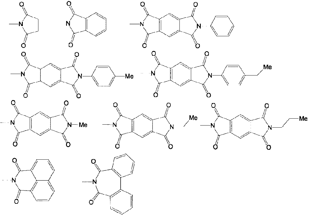
「置換オキシカルボニル基」とは、R’-O-(C=O)-で表される基を意味する。
ここで、R’は、アルキル基、アリールアルキル基、又は1価の複素環基を表す。
ここで、R’は、アルキル基、アリールアルキル基、又は1価の複素環基を表す。
置換オキシカルボニル基の炭素原子数は、通常2~60であり、好ましくは2~48である。
置換オキシカルボニル基の具体例としては、メトキシカルボニル基、エトキシカルボニル基、プロポキシカルボニル基、イソプロポキシカルボニル基、ブトキシカルボニル基、イソブトキシカルボニル基、tert-ブトキシカルボニル基、ペンチルオキシカルボニル基、ヘキシルオキシカルボニル基、シクロヘキシルオキシカルボニル基、ヘプチルオキシカルボニル基、オクチルオキシカルボニル基、2-エチルヘキシルオキシカルボニル基、ノニルオキシカルボニル基、デシルオキシカルボニル基、3,7-ジメチルオクチルオキシカルボニル基、ドデシルオキシカルボニル基、トリフルオロメトキシカルボニル基、ペンタフルオロエトキシカルボニル基、パーフルオロブトキシカルボニル基、パーフルオロヘキシルオキシカルボニル基、パーフルオロオクチルオキシカルボニル基、フェノキシカルボニル基、ナフトキシカルボニル基、及びピリジルオキシカルボニル基が挙げられる。
「アルケニル基」は、直鎖状、分岐状、及び環状のいずれであってもよい。直鎖状のアルケニル基の炭素原子数は、置換基の炭素原子数を含めないで、通常2~30であり、好ましくは3~20である。分岐状又は環状のアルケニル基の炭素原子数は、置換基の炭素原子数を含めないで、通常3~30であり、好ましくは4~20である。
アルケニル基は、置換基を有していてもよい。アルケニル基の具体例としては、ビニル基、1-プロペニル基、2-プロペニル基、2-ブテニル基、3-ブテニル基、3-ペンテニル基、4-ペンテニル基、1-ヘキセニル基、5-ヘキセニル基、7-オクテニル基、及びこれらの基がアルキル基、アルコキシ基等の置換基をさらに有している基が挙げられる。
「アルキニル基」は、直鎖状、分岐状、及び環状のいずれであってもよい。直鎖状のアルケニル基の炭素原子数は、置換基の炭素原子数を含めないで、通常2~20であり、好ましくは3~20である。分岐状又は環状のアルケニル基の炭素原子数は、置換基の炭素原子数を含めないで、通常4~30であり、好ましくは4~20である。
アルキニル基は置換基を有していてもよい。アルキニル基の具体例としては、エチニル基、1-プロピニル基、2-プロピニル基、2-ブチニル基、3-ブチニル基、3-ペンチニル基、4-ペンチニル基、1-ヘキシニル基、5-ヘキシニル基、及びこれらの基がアルキル基、アルコキシ基等の置換基をさらに有している基が挙げられる。
(p型半導体材料)
本実施形態の光電変換素子の活性層が含み得るp型半導体材料は、好ましくは所定のポリスチレン換算の重量平均分子量を有する高分子化合物である。
本実施形態の光電変換素子の活性層が含み得るp型半導体材料は、好ましくは所定のポリスチレン換算の重量平均分子量を有する高分子化合物である。
ここで、ポリスチレン換算の重量平均分子量とは、ゲルパーミエーションクロマトグラフィ(GPC)を用い、ポリスチレンの標準試料を用いて算出した重量平均分子量を意味する。
高分子化合物であるp型半導体材料のポリスチレン換算の重量平均分子量は、特に暗電流比を低減する観点から、40000以上200000以下であることが好ましく、40000以上150000以下であることがより好ましく、特に溶媒に対する溶解性を向上させる観点から、さらに好ましくは45000以上150000以下である。
本実施形態のp型半導体材料としては、例えば、ポリビニルカルバゾール及びその誘導体、ポリシラン及びその誘導体、側鎖又は主鎖に芳香族アミン構造を含むポリシロキサン誘導体、ポリアニリン及びその誘導体、ポリチオフェン及びその誘導体、ポリピロール及びその誘導体、ポリフェニレンビニレン及びその誘導体、ポリチエニレンビニレン及びその誘導体、ポリフルオレン及びその誘導体が挙げられる。
p型半導体材料は、下記式(I)で表される構成単位及び/又は下記式(II)で表される構成単位を含む高分子化合物であることが好ましい。

式(I)中、Zは下記式(Z-1)~式(Z-7)のうちのいずれかで表される基を表す。Ar1及びAr2は、同一であっても異なっていてもよい3価の芳香族複素環基を表す。

式(II)中、Ar3は2価の芳香族複素環基を表す。

式(Z-1)~(Z-7)中、Rは、水素原子、ハロゲン原子、アミノ基、アルキル基、アリール基、アルコキシ基、アリールオキシ基、アルキルチオ基、アリールチオ基、1価の複素環基、置換アミノ基、アシル基、イミン残基、アミド基、酸イミド基、置換オキシカルボニル基、アルケニル基、アルキニル基、シアノ基、又はニトロ基を表す。式(Z-1)~式(Z-7)のそれぞれにおいて、Rが2個ある場合、それらは互いに同一であっても異なっていてもよい。
式(I)で表される構成単位は、下記式(I-1)で表される構成単位であることが好ましい。

式(I-1)中、Zは前記と同様の意味を表す。
Zは、式(Z-4)~式(Z-7)のうちのいずれかで表される基であることが好ましい。
式(I-1)で表される構成単位の例としては、下記式(501)~式(505)で表される構成単位が挙げられる。

前記式(501)~式(505)中、Rは前記と同様の意味を表す。Rが2個ある場合、2個のRは互いに同一であっても異なっていてもよい。
前記式(501)~式(505)で表される構成単位のうち、下記式で表される構成単位が好ましい。

式中、Rは、前記と同様の意味を表す。2個のRは、互いに同一であっても異なっていてもよい。
Ar3で表される2価の芳香族複素環基が有する炭素原子数は、通常2~60であり、好ましくは4~60であり、より好ましくは4~20である。Ar3で表される2価の芳香族複素環基は置換基を有していてもよい。Ar3で表される2価の芳香族複素環基が有していてもよい置換基の例としては、ハロゲン原子、アミノ基、アルキル基、アリール基、アルコキシ基、アリールオキシ基、アルキルチオ基、アリールチオ基、1価の複素環基、置換アミノ基、アシル基、イミン残基、アミド基、酸イミド基、置換オキシカルボニル基、アルケニル基、アルキニル基、シアノ基、及びニトロ基が挙げられる。
Ar3で表される2価の芳香族複素環基の例としては、下記式(101)~式(185)で表される基が挙げられる。
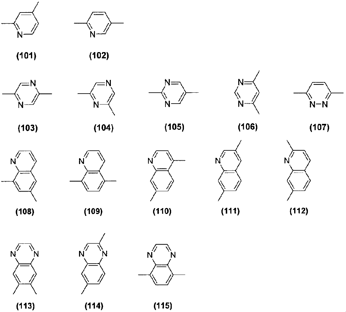
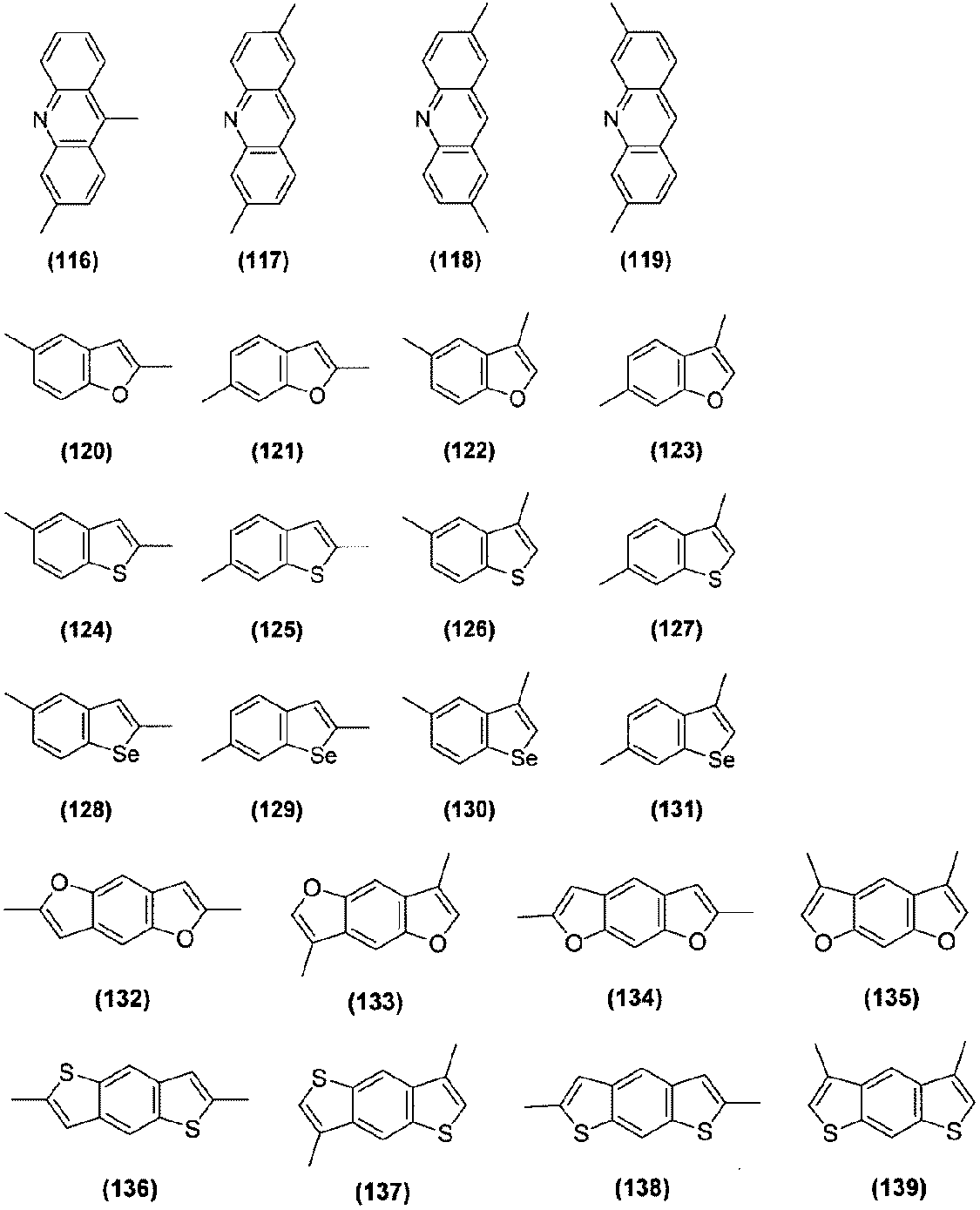
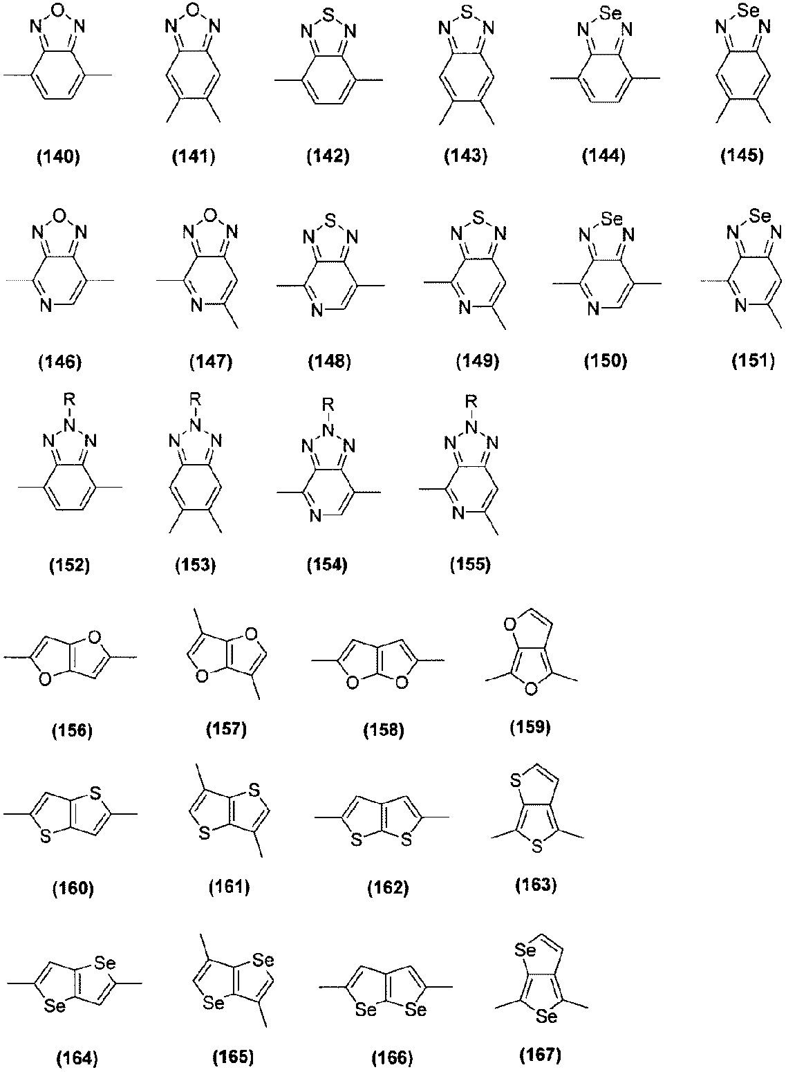
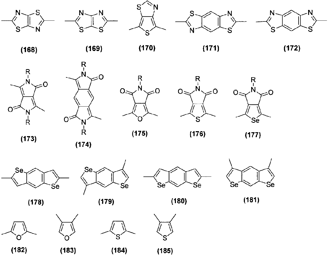
式(101)~式(185)中、Rは前記と同じ意味を表す。Rが複数個存在する場合、複数個のRは、互いに同一であっても異なっていてもよい。
前記式(II)で表される構成単位としては、下記式(II-1)~式(II-6)で表される構成単位が好ましい。
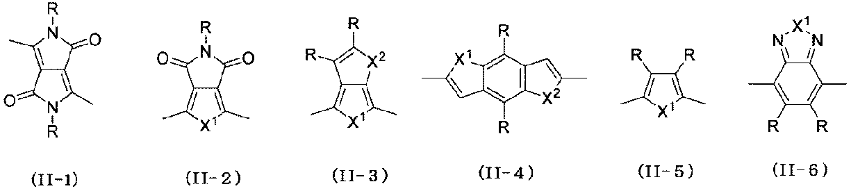
式(II-1)~式(II-6)中、X1及びX2は、それぞれ独立に、酸素原子又は硫黄原子を表し、Rは前記と同様の意味を表す。Rが複数個存在する場合、複数個のRは、互いに同一であっても異なっていてもよい。
原料化合物の入手性の観点から、式(II-1)~式(II-6)中のX1及びX2は、いずれも硫黄原子であることが好ましい。
P型半導体材料は、チオフェン骨格を含む構成単位を含む高分子化合物であることが好ましい。
P型半導体材料である高分子化合物は、2種以上の式(I)の構成単位を含んでいてもよく、2種以上の式(II)の構成単位を含んでいてもよい。
溶媒に対する溶解性を向上させるため、P型半導体材料である高分子化合物は、下記式(III)で表される構成単位を含んでいてもよい。

式(III)中、Ar4はアリーレン基を表す。
Ar4で表されるアリーレン基とは、置換基を有していてもよい芳香族炭化水素から、水素原子を2個除いた残りの原子団を意味する。芳香族炭化水素には、縮合環を有する化合物、独立したベンゼン環及び縮合環からなる群から選ばれる2個以上が、直接又はビニレン基等の2価の基を介して結合した化合物も含まれる。
芳香族炭化水素が有していてもよい置換基の例としては、複素環式化合物が有していてもよい置換基として例示された置換基と同様の置換基が挙げられる。
アリーレン基における、置換基を除いた部分の炭素原子数は、通常6~60であり、好ましくは6~20である。置換基を含めたアリーレン基の炭素原子数は、通常6~100である。
アリーレン基の例としては、フェニレン基(例えば、下記式1~式3)、ナフタレン-ジイル基(例えば、下記式4~式13)、アントラセン-ジイル基(例えば、下記式14~式19)、ビフェニル-ジイル基(例えば、下記式20~式25)、ターフェニル-ジイル基(例えば、下記式26~式28)、縮合環化合物基(例えば、下記式29~式35)、フルオレン-ジイル基(例えば、下記式36~式38)、及びベンゾフルオレン-ジイル基(例えば、下記式39~式46)が挙げられる。


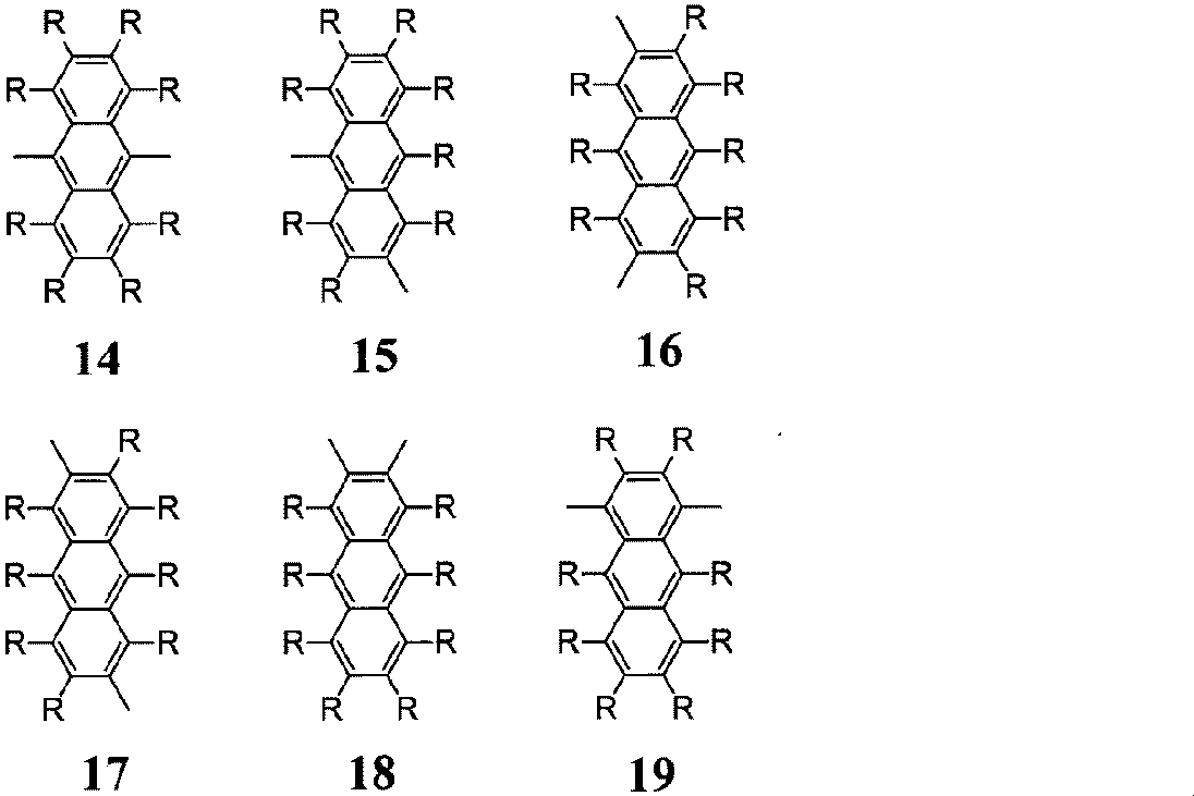
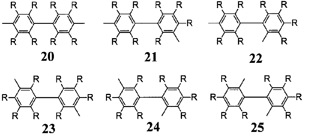

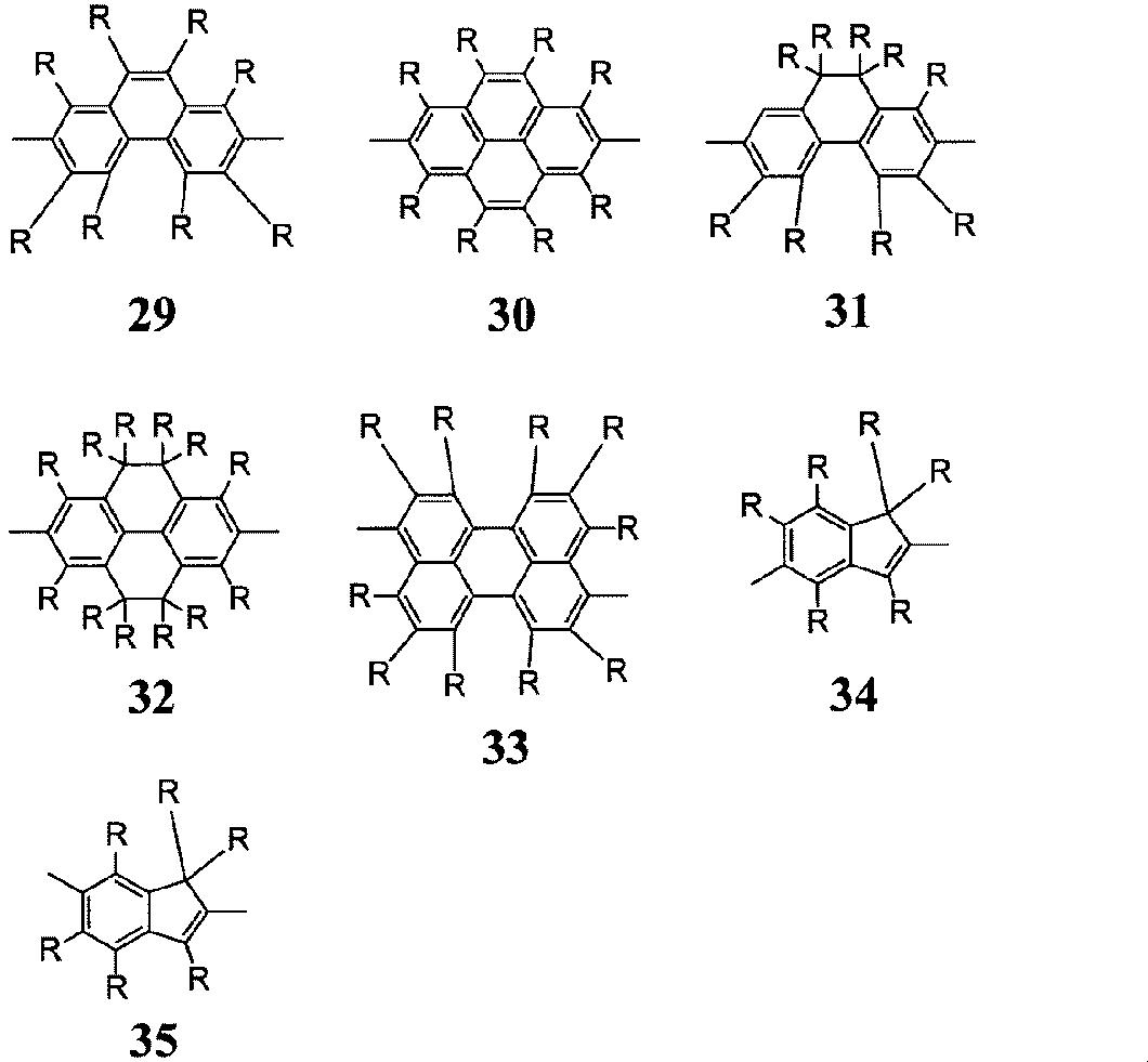


式1~46中、置換基であるRは、前記と同様の意味を表す。複数個存在するRは、互いに同一であっても異なっていてもよい。
p型半導体材料である高分子化合物を構成する構成単位は、式(I)で表される構成単位、式(II)で表される構成単位及び式(III)で表される構成単位から選択される2種以上の構成単位が2個以上組み合わせされて連結された構成単位であってもよい。
p型半導体材料としての高分子化合物が、式(I)で表される構成単位及び/又は式(II)で表される構成単位を含む場合、式(I)で表される構成単位及び式(II)で表される構成単位の合計量は、高分子化合物が含むすべての構成単位(100モル%)のうち、通常20~100モル%であり、p型半導体材料としての電荷輸送性を向上させることができるので、好ましくは40~100モル%であり、より好ましくは50~100モル%である。
p型半導体材料である高分子化合物の具体例としては、下記式P-1~P-6で表される高分子化合物が挙げられる。


本実施形態の活性層形成用塗布液は、p型半導体材料を1種のみ含んでいてもよく、2種以上を任意の割合の組み合わせで含んでいてもよい。
(n型半導体材料)
本実施形態の活性層が含み得るn型半導体材料(電子受容性化合物)は、既に説明した電子輸送層の仕事関数とn型半導体材料のLUMOのエネルギーレベルとの差が、0.06eV以上となるように、電子輸送層の仕事関数を勘案して、選択することができる。
本実施形態の活性層が含み得るn型半導体材料(電子受容性化合物)は、既に説明した電子輸送層の仕事関数とn型半導体材料のLUMOのエネルギーレベルとの差が、0.06eV以上となるように、電子輸送層の仕事関数を勘案して、選択することができる。
n型半導体材料は、低分子化合物であっても高分子化合物であってもよい。
低分子化合物であるn型半導体材料の例としては、オキサジアゾール誘導体、アントラキノジメタン及びその誘導体、ベンゾキノン及びその誘導体、ナフトキノン及びその誘導体、アントラキノン及びその誘導体、テトラシアノアントラキノジメタン及びその誘導体、フルオレノン誘導体、ジフェニルジシアノエチレン及びその誘導体、ジフェノキノン誘導体、8-ヒドロキシキノリン及びその誘導体の金属錯体、C60フラーレン等のフラーレン類及びその誘導体、並びに、バソクプロイン等のフェナントレン誘導体が挙げられる。
高分子化合物であるn型半導体材料の例としては、ポリビニルカルバゾール及びその誘導体、ポリシラン及びその誘導体、側鎖又は主鎖に芳香族アミン構造を有するポリシロキサン誘導体、ポリアニリン及びその誘導体、ポリチオフェン及びその誘導体、ポリピロール及びその誘導体、ポリフェニレンビニレン及びその誘導体、ポリチエニレンビニレン及びその誘導体、ポリキノリン及びその誘導体、ポリキノキサリン及びその誘導体、並びに、ポリフルオレン及びその誘導体が挙げられる。
n型半導体材料としては、フラーレン及びフラーレン誘導体から選ばれる1種以上が好ましく、フラーレン誘導体がより好ましい。
フラーレンの例としては、C60フラーレン、C70フラーレン、C76フラーレン、C78フラーレン、及びC84フラーレンが挙げられる。フラーレン誘導体の例としては、これらのフラーレンの誘導体が挙げられる。フラーレン誘導体とは、フラーレンの少なくとも一部が修飾された化合物を意味する。
フラーレン誘導体の例としては、下記式(N-1)~式(N-4)で表される化合物が挙げられる。

式(N-1)~式(N-4)中、Raは、アルキル基、アリール基、1価の複素環基、又はエステル構造を有する基を表す。複数個あるRaは、互いに同一であっても異なっていてもよい。
Rbは、アルキル基、又はアリール基を表す。複数個あるRbは、互いに同一であっても異なっていてもよい。
Raで表されるエステル構造を有する基の例としては、下記式(19)で表される基が挙げられる。

式(19)中、u1は、1~6の整数を表す。u2は、0~6の整数を表す。Rcは、アルキル基、アリール基、又は1価の複素環基を表す。
C60フラーレン誘導体の例としては、下記の化合物が挙げられる。
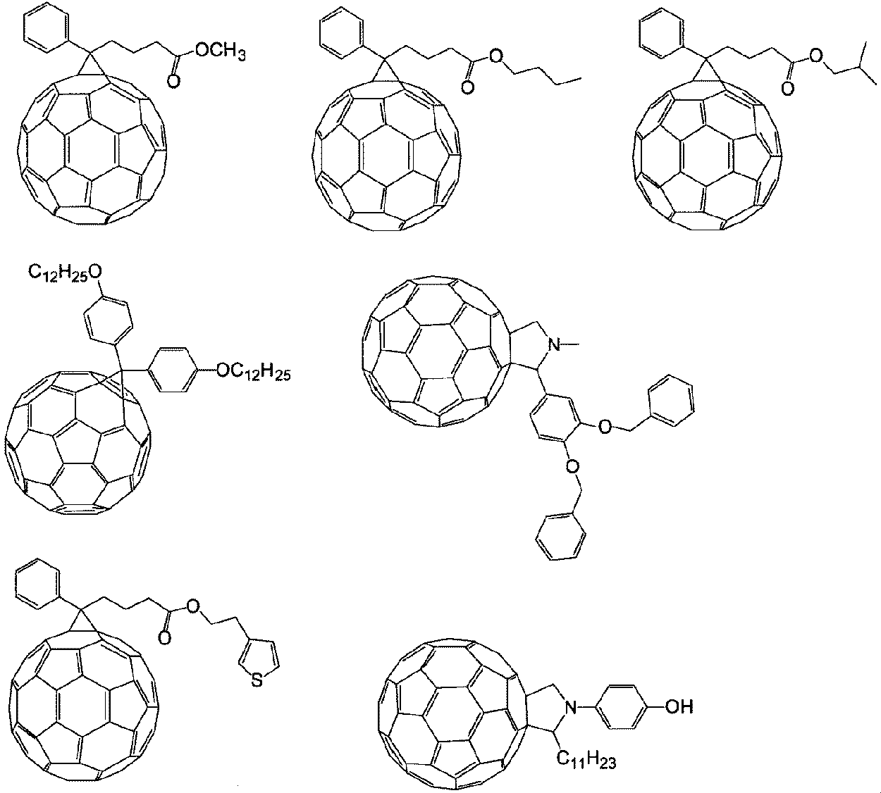
C70フラーレン誘導体の例としては、下記の化合物が挙げられる。
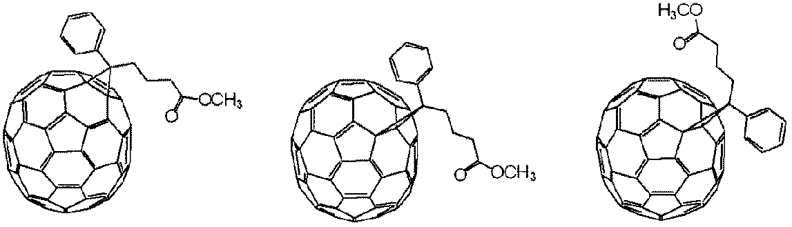
フラーレン誘導体の具体例としては、[6,6]-フェニル-C61酪酸メチルエステル(C60PCBM、[6,6]-Phenyl C61 butyric acid methyl ester)、[6,6]-フェニル-C71酪酸メチルエステル(C70PCBM、[6,6]-Phenyl C71 butyric acid methyl ester)、[6,6」-フェニル-C85酪酸メチルエステル(C84PCBM、[6,6]-Phenyl C85 butyric acid methyl ester)、及び[6,6]-チエニル-C61酪酸メチルエステル([6,6]-Thienyl C61 butyric acid methyl ester)が挙げられる。
本実施形態の活性層形成用塗布液は、n型半導体材料を1種のみ含んでいてもよく、2種以上を任意の割合の組み合わせで含んでいてもよい。
(第1溶媒)
溶媒は、選択されたp型半導体材料及びn型半導体材料に対する溶解性、活性層を形成する際の乾燥条件に対応するための特性(沸点など)を考慮して選択すればよい。
溶媒は、選択されたp型半導体材料及びn型半導体材料に対する溶解性、活性層を形成する際の乾燥条件に対応するための特性(沸点など)を考慮して選択すればよい。
主溶媒(良溶媒)である第1溶媒は、置換基(例えば、アルキル基、ハロゲン原子)を有していてもよい芳香族炭化水素(以下、単に芳香族炭化水素という。)である。第1溶媒は、選択されたp型半導体材料及びn型半導体材料の溶解性を考慮して選択することが好ましい。
このような芳香族炭化水素としては、例えば、トルエン、キシレン(例、o-キシレン、m-キシレン、p-キシレン)、トリメチルベンゼン(例、メシチレン、1,2,4-トリメチルベンゼン(プソイドクメン))、ブチルベンゼン(例、n-ブチルベンゼン、sec-ブチルベンゼン、tert-ブチルベンゼン)、メチルナフタレン(例、1-メチルナフタレン)、テトラリン、インダン、クロロベンゼン及びジクロロベンゼン(o-ジクロロベンゼン)が挙げられる。
第1溶媒は1種のみの芳香族炭化水素から構成されていても、2種以上の芳香族炭化水素から構成されていてもよい。第1溶媒は、1種のみの芳香族炭化水素から構成されることが好ましい。
第1溶媒は、好ましくは、トルエン、o-キシレン、m-キシレン、p-キシレン、メシチレン、プソイドクメン、n-ブチルベンゼン、sec-ブチルベンゼン、tert-ブチルベンゼン、メチルナフタレン、テトラリン、インダン、クロロベンゼン及びo-ジクロロベンゼンからなる群から選択される1種以上を含み、より好ましくは、o-キシレン、プソイドクメン、テトラリン、クロロベンゼン又はo-ジクロロベンゼンを含む。
(第2溶媒)
第2溶媒(貧溶媒)は、特にn型半導体材料の溶解性を高める観点から選択される溶媒である。第2溶媒としては、例えば、アセトン、メチルエチルケトン、シクロヘキサノン、アセトフェノン、プロピオフェノン等のケトン溶媒、酢酸エチル、酢酸ブチル、酢酸フェニル、エチルセルソルブアセテート、安息香酸メチル、安息香酸ブチル、安息香酸ベンジル等のエステル溶媒が挙げられる。
第2溶媒(貧溶媒)は、特にn型半導体材料の溶解性を高める観点から選択される溶媒である。第2溶媒としては、例えば、アセトン、メチルエチルケトン、シクロヘキサノン、アセトフェノン、プロピオフェノン等のケトン溶媒、酢酸エチル、酢酸ブチル、酢酸フェニル、エチルセルソルブアセテート、安息香酸メチル、安息香酸ブチル、安息香酸ベンジル等のエステル溶媒が挙げられる。
第2溶媒は、アセトフェノン、プロピオフェノン、又は安息香酸ベンジルが好ましい。
(第1溶媒及び第2溶媒の組み合わせ)
第1溶媒及び第2溶媒の組み合わせとしては、例えば、下記表1に示される組み合わせが挙げられる。
第1溶媒及び第2溶媒の組み合わせとしては、例えば、下記表1に示される組み合わせが挙げられる。
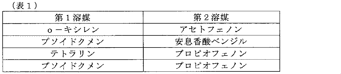
(第1溶媒及び第2溶媒の重量比)
第1溶媒の第2溶媒に対する重量比(第1溶媒/第2溶媒)は、p型半導体材料及びn型半導体材料の溶解性をより向上させる観点から、85/15~97/3の範囲とすることが好ましい。
第1溶媒の第2溶媒に対する重量比(第1溶媒/第2溶媒)は、p型半導体材料及びn型半導体材料の溶解性をより向上させる観点から、85/15~97/3の範囲とすることが好ましい。
(活性層形成用塗布液における第1溶媒及び第2溶媒の合計の重量百分率)
本実施形態の活性層形成用塗布液に含まれる第1溶媒及び第2溶媒の総重量は、活性層形成用塗布液の全重量を100重量%としたときに、p型半導体材料及びn型半導体材料の溶解性をより向上させる観点から、好ましくは90重量%以上、より好ましくは92重量%以上、さらに好ましくは95重量%以上であり、活性層形成用塗布液中のp型半導体材料及びn型半導体材料の濃度を高くすることにより一定の厚さ以上の層を形成し易くする観点から、好ましくは99重量%以下、より好ましくは98重量%以下、さらに好ましくは97.5重量%以下である。
本実施形態の活性層形成用塗布液に含まれる第1溶媒及び第2溶媒の総重量は、活性層形成用塗布液の全重量を100重量%としたときに、p型半導体材料及びn型半導体材料の溶解性をより向上させる観点から、好ましくは90重量%以上、より好ましくは92重量%以上、さらに好ましくは95重量%以上であり、活性層形成用塗布液中のp型半導体材料及びn型半導体材料の濃度を高くすることにより一定の厚さ以上の層を形成し易くする観点から、好ましくは99重量%以下、より好ましくは98重量%以下、さらに好ましくは97.5重量%以下である。
(任意の溶媒)
本実施形態の活性層形成用塗布液は、第1溶媒及び第2溶媒以外の任意の溶媒を含んでいてもよい。活性層形成用塗布液に含まれる全溶媒の合計重量を100重量%としたときに、任意の溶媒の含有率は、好ましくは5重量%以下であり、より好ましくは3重量%以下であり、さらに好ましくは1重量%以下である。任意の溶媒としては、第2溶媒より沸点が高い溶媒が好ましい。
本実施形態の活性層形成用塗布液は、第1溶媒及び第2溶媒以外の任意の溶媒を含んでいてもよい。活性層形成用塗布液に含まれる全溶媒の合計重量を100重量%としたときに、任意の溶媒の含有率は、好ましくは5重量%以下であり、より好ましくは3重量%以下であり、さらに好ましくは1重量%以下である。任意の溶媒としては、第2溶媒より沸点が高い溶媒が好ましい。
(任意の成分)
本実施形態の活性層形成用塗布液には、第1溶媒、第2溶媒、p型半導体材料、及びn型半導体材料の他に、本発明の目的及び効果を損なわない限度において、紫外線吸収剤、酸化防止剤、吸収した光により電荷を発生させる機能を増感するための増感剤、紫外線に対する安定性を増すための光安定剤といった任意の成分が含まれていてもよい。
本実施形態の活性層形成用塗布液には、第1溶媒、第2溶媒、p型半導体材料、及びn型半導体材料の他に、本発明の目的及び効果を損なわない限度において、紫外線吸収剤、酸化防止剤、吸収した光により電荷を発生させる機能を増感するための増感剤、紫外線に対する安定性を増すための光安定剤といった任意の成分が含まれていてもよい。
(活性層形成用塗布液におけるp型半導体材料及びn型半導体材料の濃度)
本実施形態の活性層形成用塗布液における、p型半導体材料及びn型半導体材料の合計の濃度は、0.01重量%以上20重量%以下であることが好ましく、0.01重量%以上10重量%以下であることがより好ましく、0.01重量%以上5重量%以下であることがさらに好ましく、0.1重量%以上5重量%以下であることが特に好ましい。活性層形成用塗布液中、p型半導体材料及びn型半導体材料は溶解していても分散していてもよい。p型半導体材料及びn型半導体材料は、好ましくは少なくとも一部が溶解しており、より好ましくは全部が溶解している。
本実施形態の活性層形成用塗布液における、p型半導体材料及びn型半導体材料の合計の濃度は、0.01重量%以上20重量%以下であることが好ましく、0.01重量%以上10重量%以下であることがより好ましく、0.01重量%以上5重量%以下であることがさらに好ましく、0.1重量%以上5重量%以下であることが特に好ましい。活性層形成用塗布液中、p型半導体材料及びn型半導体材料は溶解していても分散していてもよい。p型半導体材料及びn型半導体材料は、好ましくは少なくとも一部が溶解しており、より好ましくは全部が溶解している。
(活性層形成用塗布液の調製)
本実施形態の活性層形成用塗布液は、公知の方法により調製することができる。例えば、第1溶媒及び第2溶媒を混合して混合溶媒を調製し、得られた混合溶媒にp型半導体材料及びn型半導体材料を添加する方法、第1溶媒にp型半導体材料を添加し、第2溶媒にn型半導体材料を添加してから、各材料が添加された第1溶媒及び第2溶媒を混合する方法などにより、調製することができる。
本実施形態の活性層形成用塗布液は、公知の方法により調製することができる。例えば、第1溶媒及び第2溶媒を混合して混合溶媒を調製し、得られた混合溶媒にp型半導体材料及びn型半導体材料を添加する方法、第1溶媒にp型半導体材料を添加し、第2溶媒にn型半導体材料を添加してから、各材料が添加された第1溶媒及び第2溶媒を混合する方法などにより、調製することができる。
第1溶媒及び第2溶媒とp型半導体材料及びn型半導体材料とを、溶媒の沸点以下の温度で加温して混合してもよい。
第1溶媒及び第2溶媒とp型半導体材料及びn型半導体材料とを混合した後、得られた混合物をフィルターを用いて濾過し、得られた濾液をインクとして用いてもよい。フィルターとしては、例えば、ポリテトラフルオロエチレン(PTFE)等のフッ素樹脂で形成されたフィルターを用いることができる。
(光電変換素子の用途)
本実施形態の光電変換素子は、光が照射されることにより、電極間に光起電力を発生させることができ、太陽電池として動作させることができる。また太陽電池を複数集積することにより薄膜太陽電池モジュールとすることもできる。
本実施形態の光電変換素子は、光が照射されることにより、電極間に光起電力を発生させることができ、太陽電池として動作させることができる。また太陽電池を複数集積することにより薄膜太陽電池モジュールとすることもできる。
また、本実施形態の光電変換素子は、電極間に電圧を印加した状態で、透明又は半透明の電極側から光を照射することにより、光電流を流すことができ、光検出素子(光センサー)として動作させることができる。また、光センサーを複数集積することによりイメージセンサーとして用いることもできる。
(光電変換素子の適用例)
既に説明した本発明の実施形態にかかる光電変換素子は、ワークステーション、パーソナルコンピュータ、携帯情報端末、入退室管理システム、デジタルカメラ、及び医療機器などの種々の電子装置が備える検出部に好適に適用することができる。
既に説明した本発明の実施形態にかかる光電変換素子は、ワークステーション、パーソナルコンピュータ、携帯情報端末、入退室管理システム、デジタルカメラ、及び医療機器などの種々の電子装置が備える検出部に好適に適用することができる。
本発明の光電変換素子(光検出素子)は、上記例示の電子装置が備える、例えば、X線撮像装置及びCMOSイメージセンサーなどの固体撮像装置用のイメージ検出部(イメージセンサー)、指紋検出部、顔検出部、静脈検出部及び虹彩検出部などの生体の一部分の所定の特徴を検出する検出部、パルスオキシメーターなどの光学バイオセンサーの検出部などに好適に適用することができる。
以下、本発明の実施形態にかかる光電変換素子が好適に適用され得る検出部のうち、固体撮像装置用のイメージ検出部、生体情報認証装置(指紋認証装置)のための指紋検出部の構成例について、図面を参照して説明する。
(イメージ検出部)
図2は、固体撮像装置用のイメージ検出部の構成例を模式的に示す図である。
図2は、固体撮像装置用のイメージ検出部の構成例を模式的に示す図である。
イメージ検出部1は、CMOSトランジスタ基板20と、CMOSトランジスタ基板20を覆うように設けられている層間絶縁膜30と、層間絶縁膜30上に設けられている、本発明の実施形態にかかる光電変換素子10と、層間絶縁膜30を貫通するように設けられており、CMOSトランジスタ基板20と光電変換素子10とを電気的に接続する層間配線部32と、光電変換素子10を覆うように設けられている封止層40と、封止層40上に設けられているカラーフィルター50とを備えている。
CMOSトランジスタ基板20は、従来公知の任意好適な構成を設計に応じた態様で備えている。
CMOSトランジスタ基板20は、基板の厚さ内に形成されたトランジスタ、コンデンサなどを含み、種々の機能を実現するためのCMOSトランジスタ回路(MOSトランジスタ回路)などの機能素子を備えている。
機能素子としては、例えば、フローティングディフュージョン、リセットトランジスタ、出力トランジスタ、選択トランジスタが挙げられる。
このような機能素子、配線などにより、CMOSトランジスタ基板20には、信号読み出し回路などが作り込まれている。
層間絶縁膜30は、例えば酸化シリコン、絶縁性樹脂などの従来公知の任意好適な絶縁性材料により構成することができる。層間配線部32は、例えば、銅、タングステンなどの従来公知の任意好適な導電性材料(配線材料)により構成することができる。層間配線部32は、例えば、配線層の形成と同時に形成されるホール内配線であっても、配線層とは別途形成される埋込みプラグであってもよい。
封止層40は、光電変換素子10を機能的に劣化させてしまうおそれのある酸素、水などの有害物質の浸透を防止又は抑制できることを条件として、従来公知の任意好適な材料により構成することができる。封止層40は、既に説明した封止基板17により構成してもよい。
カラーフィルター50としては、従来公知の任意好適な材料により構成され、かつイメージ検出部1の設計に対応した例えば原色カラーフィルターを用いることができる。また、カラーフィルター50としては、原色カラーフィルターと比較して、厚さを薄くすることができる補色カラーフィルターを用いることもできる。補色カラーフィルターとしては、例えば(イエロー、シアン、マゼンタ)の3種類、(イエロー、シアン、透明)の3種類、(イエロー、透明、マゼンタ)の3種類、及び(透明、シアン、マゼンタ)の3種類が組み合わされたカラーフィルターを用いることができる。これらは、カラー画像データを生成できることを条件として、光電変換素子10及びCMOSトランジスタ基板20の設計に対応した任意好適な配置とすることができる。
カラーフィルター50を介して光電変換素子10が受光した光は、光電変換素子10によって、受光量に応じた電気信号に変換され、電極を介して、光電変換素子10外に受光信号、すなわち撮像対象に対応する電気信号として出力される。
次いで、光電変換素子10から出力された受光信号は、層間配線部32を介して、CMOSトランジスタ基板20に入力され、CMOSトランジスタ基板20に作り込まれた信号読み出し回路により読み出され、図示しないさらなる任意好適な従来公知の機能部によって信号処理されることにより、撮像対象に基づく画像情報が生成される。
(指紋検出部)
図3は、表示装置に一体的に構成される指紋検出部の構成例を模式的に示す図である。
図3は、表示装置に一体的に構成される指紋検出部の構成例を模式的に示す図である。
携帯情報端末の表示装置2は、本発明の実施形態にかかる光電変換素子10を主たる構成要素として含む指紋検出部100と、当該指紋検出部100上に設けられ、所定の画像を表示する表示パネル部200とを備えている。
この構成例では、表示パネル部200の表示領域200aと略一致する領域に指紋検出部100が設けられている。換言すると、指紋検出部100の上方に、表示パネル部200が一体的に積層されている。
表示領域200aのうちの一部の領域においてのみ指紋検出を行う場合には、当該一部の領域のみに対応させて指紋検出部100を設ければよい。
指紋検出部100は、本発明の実施形態にかかる光電変換素子10を本質的な機能を奏する機能部として含む。指紋検出部100は、図示されていない保護フィルム(protection film)、支持基板、封止基板、封止部材、バリアフィルム、バンドパスフィルター、赤外線カットフィルムなどの任意好適な従来公知の部材を所望の特性が得られるような設計に対応した態様で備え得る。指紋検出部100には、既に説明したイメージ検出部の構成を採用することもできる。
光電変換素子10は、表示領域200a内において、任意の態様で含まれ得る。例えば、複数の光電変換素子10が、マトリクス状に配置されていてもよい。
光電変換素子10は、既に説明したとおり、支持基板11又は封止基板に設けられており、支持基板11には、例えばマトリクス状に電極(陽極又は陰極)が設けられている。
光電変換素子10が受光した光は、光電変換素子10によって、受光量に応じた電気信号に変換され、電極を介して、光電変換素子10外に受光信号、すなわち撮像された指紋に対応する電気信号として出力される。
表示パネル部200は、この構成例では、タッチセンサーパネルを含む有機エレクトロルミネッセンス表示パネル(有機EL表示パネル)として構成されている。表示パネル部200は、例えば有機EL表示パネルの代わりに、バックライトなどの光源を含む液晶表示パネルなどの任意好適な従来公知の構成を有する表示パネルにより構成されていてもよい。
表示パネル部200は、既に説明した指紋検出部100上に設けられている。表示パネル部200は、有機エレクトロルミネッセンス素子(有機EL素子)220を本質的な機能を奏する機能部として含む。表示パネル部200は、さらに任意好適な従来公知のガラス基板といった基板(支持基板210又は封止基板240)、封止部材、バリアフィルム、円偏光板などの偏光板、タッチセンサーパネル230などの任意好適な従来公知の部材を所望の特性に対応した態様で備え得る。
以上説明した構成例において、有機EL素子220は、表示領域200aにおける画素の光源として用いられるとともに、指紋検出部100における指紋の撮像のための光源としても用いられる。
ここで、指紋検出部100の動作について簡単に説明する。
指紋認証の実行時には、表示パネル部200の有機EL素子220から放射される光を用いて指紋検出部100が指紋を検出する。具体的には、有機EL素子220から放射された光は、有機EL素子220と指紋検出部100の光電変換素子10との間に存在する構成要素を透過して、表示領域200a内である表示パネル部200の表面に接するように載置された手指の指先の皮膚(指表面)によって反射される。指表面によって反射された光のうちの少なくとも一部は、間に存在する構成要素を透過して光電変換素子10によって受光され、光電変換素子10の受光量に応じた電気信号に変換される。そして、変換された電気信号から、指表面の指紋についての画像情報が構成される。
指紋認証の実行時には、表示パネル部200の有機EL素子220から放射される光を用いて指紋検出部100が指紋を検出する。具体的には、有機EL素子220から放射された光は、有機EL素子220と指紋検出部100の光電変換素子10との間に存在する構成要素を透過して、表示領域200a内である表示パネル部200の表面に接するように載置された手指の指先の皮膚(指表面)によって反射される。指表面によって反射された光のうちの少なくとも一部は、間に存在する構成要素を透過して光電変換素子10によって受光され、光電変換素子10の受光量に応じた電気信号に変換される。そして、変換された電気信号から、指表面の指紋についての画像情報が構成される。
表示装置2を備える携帯情報端末は、従来公知の任意好適なステップにより、得られた画像情報と、予め記録されていた指紋認証用の指紋データとを比較して、指紋認証を行う。
以下、本発明をさらに詳細に説明するために実施例を示す。本発明は下記の実施例に限定されない。
<実施例1>光電変換素子の製造及び評価
(光電変換素子の製造)
スパッタリング法により、ガラス基板上にITO薄膜(陰極)を150nmの厚さで形成した。このガラス基板の表面に対し、オゾンUV処理を行った。
(光電変換素子の製造)
スパッタリング法により、ガラス基板上にITO薄膜(陰極)を150nmの厚さで形成した。このガラス基板の表面に対し、オゾンUV処理を行った。
次いで、3-ペンタノール10gに対して、1重量%のポリエチレンイミンエトキシレート(PEIE)水溶液(アルドリッチ社製、商品名ポリエチレンイミン、80%エトキシ化溶液、重量平均分子量110000)0.1g及び10重量%の酸化亜鉛/イソプロパノール分散液(テイカ社製、製品名:HTD-711Z)を含む溶液1gを混合して、電子輸送層形成用塗布液を調製した。
得られた電子輸送層形成用塗布液をスピンコート法により、オゾンUV処理を行ったガラス基板のITO薄膜上に塗布し、塗布膜を形成した。
塗布膜が形成されたガラス基板を、ホットプレートを用いて、120℃で10分間加熱処理して、形成された塗布膜を硬化することにより、陰極であるITO薄膜上に電子輸送層を形成した。得られた電子輸送層の厚さは50nmであった。
p型半導体材料である下記式で表される高分子化合物P-1の重量とn型半導体材料であるC60PCBM(フロンティアカーボン社製、商品名:E100)の重量との比(p/n比)が1/1.75となるように混合した。得られた混合物を、o-キシレンとアセトフェノンとの混合溶媒(o-キシレン/アセトフェノン=95/5(重量比))に、p型半導体材料の含有量が混合溶媒に対して2重量%となるように加えて、60℃で10時間撹拌して溶解させることにより、活性層形成用塗布液を得た。

得られた活性層形成用塗布液を、ガラス基板に形成された電子輸送層上にスピンコート法により塗布して、塗布膜を形成した。得られた塗布膜を、100℃に加熱したホットプレートを用いて、10分間加熱する乾燥処理を行うことにより、活性層を形成した。得られた活性層の厚さは550nmであった。
抵抗加熱蒸着装置を用いて、得られた活性層上に酸化モリブデン(MoO3)を約30nmの厚さで蒸着することにより、正孔輸送層を形成した。
得られた正孔輸送層上に、銀(Ag)層を約80nmの厚さで蒸着することにより、陽極を形成し、光電変換素子(光検出素子)を製造した。
UV硬化剤を封止基板(ガラス基板)上に塗布して得られた光電変換素子をUV硬化剤が囲むように貼り合わせた後、UV光を照射することで光電変換素子を封止した。
得られた光電変換素子を厚さ方向で見たときの平面的な形状は2mm×2mmの正方形であった。
(光電変換素子の評価)
製造された光電変換素子及び関連するパラメータについて、下記のとおり測定及び算出した。結果を下記表2に示す。
製造された光電変換素子及び関連するパラメータについて、下記のとおり測定及び算出した。結果を下記表2に示す。
(1)暗電流比の評価
製造された光電変換素子の暗電流比について評価した。ここで、暗電流比とは、10Vの電圧印加時に得られた暗電流と、2Vの電圧印加時に得られた暗電流との比(暗電流(10V)/暗電流(2V))を意味する。
暗電流の測定は、半導体パラメーターアナライザー(B1500A、アジレントテクノロジー社製)を用いて、10V及び2Vの逆バイアス電圧印加時における暗電流を測定した。得られた暗電流の値に基づいて暗電流比を計算した。
製造された光電変換素子の暗電流比について評価した。ここで、暗電流比とは、10Vの電圧印加時に得られた暗電流と、2Vの電圧印加時に得られた暗電流との比(暗電流(10V)/暗電流(2V))を意味する。
暗電流の測定は、半導体パラメーターアナライザー(B1500A、アジレントテクノロジー社製)を用いて、10V及び2Vの逆バイアス電圧印加時における暗電流を測定した。得られた暗電流の値に基づいて暗電流比を計算した。
(2)n型半導体材料のLUMOのエネルギーレベルの測定
活性層が含むn型半導体材料であるC60PCBMのLUMOのエネルギーレベルをサイクリックボルタンメトリー(CV)から見積もった。
活性層が含むn型半導体材料であるC60PCBMのLUMOのエネルギーレベルをサイクリックボルタンメトリー(CV)から見積もった。
CV測定は、Advanced Materials、18巻、2006年、789頁~794頁に記載の方法と同じ条件で行った。用いられた機材等は下記のとおりである。
CV測定装置:BAS社製、Electrochemical Analyzer Model 600B
支持電解質:ヘキサフルオロりん酸テトラブチルアンモニウム(TBAPF6、Aldrich社製)を濃度0.1M含む、脱水アセトニトリル溶液
作用電極:白金ホイル/n型半導体材料(クロロホルムに溶解させた溶液を滴下)
対極:白金ホイル
参照電極:Ag/AgCl電極
標準電位:フェロセン
支持電解質:ヘキサフルオロりん酸テトラブチルアンモニウム(TBAPF6、Aldrich社製)を濃度0.1M含む、脱水アセトニトリル溶液
作用電極:白金ホイル/n型半導体材料(クロロホルムに溶解させた溶液を滴下)
対極:白金ホイル
参照電極:Ag/AgCl電極
標準電位:フェロセン
結果として、C60PCBMのLUMOのエネルギーレベルは、-4.3eVであった。
(3)電子輸送層の仕事関数(WF)の測定
電子輸送層形成用塗布液をガラス基板に塗布し、ホットプレートを用いて、120℃で10分間加熱処理して得られた電子輸送層を、ケルビンプローブ装置を用いて測定することで求めた。ケルビンプローブ装置は、理研計器株式会社のFAC-2を使用した。校正用基準サンプルとして金(WF:5.1eV)を用いた。電子輸送層の仕事関数は、3.77eVであった。
電子輸送層形成用塗布液をガラス基板に塗布し、ホットプレートを用いて、120℃で10分間加熱処理して得られた電子輸送層を、ケルビンプローブ装置を用いて測定することで求めた。ケルビンプローブ装置は、理研計器株式会社のFAC-2を使用した。校正用基準サンプルとして金(WF:5.1eV)を用いた。電子輸送層の仕事関数は、3.77eVであった。
(4)陰極の仕事関数(WF)の測定
陰極の仕事関数は、ガラス基板にITO薄膜(陰極)を150nmの厚さで形成し、形成されたITO薄膜を、ケルビンプローブ装置を用いて測定することにより求めた。ケルビンプローブ装置は、理研計器株式会社のFAC-2を使用した。校正用基準サンプルとして金(WF:5.1eV)を用いた。陰極の仕事関数は、4.80eVであった。
陰極の仕事関数は、ガラス基板にITO薄膜(陰極)を150nmの厚さで形成し、形成されたITO薄膜を、ケルビンプローブ装置を用いて測定することにより求めた。ケルビンプローブ装置は、理研計器株式会社のFAC-2を使用した。校正用基準サンプルとして金(WF:5.1eV)を用いた。陰極の仕事関数は、4.80eVであった。
(5)ΔWF及びΔEの算出
得られたC60PCBM(活性層に含まれるn型半導体材料)のLUMOのエネルギーレベル(LUMO)、電子輸送層の仕事関数(Wf1)及び陰極の仕事関数(Wf2)に基づいて、下記式によりΔWF及びΔEを算出した。
ΔWF=Wf2-Wf1
ΔE=|LUMO|-Wf1
得られたC60PCBM(活性層に含まれるn型半導体材料)のLUMOのエネルギーレベル(LUMO)、電子輸送層の仕事関数(Wf1)及び陰極の仕事関数(Wf2)に基づいて、下記式によりΔWF及びΔEを算出した。
ΔWF=Wf2-Wf1
ΔE=|LUMO|-Wf1
<実施例2>
電子輸送層形成用塗布液において溶媒として用いられた3-ペンタノールの代わりに、2-プロパノールを用いた以外は実施例1と同様にして、光電変換素子を製造し、評価した。
電子輸送層形成用塗布液において溶媒として用いられた3-ペンタノールの代わりに、2-プロパノールを用いた以外は実施例1と同様にして、光電変換素子を製造し、評価した。
<実施例3>
電子輸送層形成用塗布液において溶媒として用いられた3-ペンタノールの代わりに、エタノールを用いた以外は実施例1と同様にして、光電変換素子を製造し、評価した。
電子輸送層形成用塗布液において溶媒として用いられた3-ペンタノールの代わりに、エタノールを用いた以外は実施例1と同様にして、光電変換素子を製造し、評価した。
<比較例1>
(光電変換素子の製造)
スパッタリング法により、ガラス基板上にITO薄膜(陰極)を150nmの厚さで形成した。このガラス基板の表面に対し、オゾンUV処理を行った。
(光電変換素子の製造)
スパッタリング法により、ガラス基板上にITO薄膜(陰極)を150nmの厚さで形成した。このガラス基板の表面に対し、オゾンUV処理を行った。
水10gに対して、1重量%のポリエチレンイミンエトキシレート(PEIE)水溶液(アルドリッチ社製、商品名ポリエチレンイミン、80%エトキシ化溶液、重量平均分子量110000)を0.1gを混合して調製した電子輸送層形成用塗布液を用いた以外は、実施例1と同様にして、光電変換素子を製造し、評価した。
<比較例2>
10重量%の酸化亜鉛/イソプロパノール分散液(テイカ社製、製品名:HTD-711Z)を3-ペンタノールで10倍に希釈した電子輸送層形成用塗布液を用いた以外は実施例1と同様にして、光電変換素子を製造し、評価した。
10重量%の酸化亜鉛/イソプロパノール分散液(テイカ社製、製品名:HTD-711Z)を3-ペンタノールで10倍に希釈した電子輸送層形成用塗布液を用いた以外は実施例1と同様にして、光電変換素子を製造し、評価した。
<比較例3>
10重量%の酸化亜鉛/イソプロパノール分散液(テイカ社製、製品名:HTD-711Z)を3-ペンタノールで10倍希釈した溶液を第1電子輸送層形成用塗布液として、スピンコート法により、オゾンUV処理を行ったガラス基板のITO薄膜上に塗布した。
10重量%の酸化亜鉛/イソプロパノール分散液(テイカ社製、製品名:HTD-711Z)を3-ペンタノールで10倍希釈した溶液を第1電子輸送層形成用塗布液として、スピンコート法により、オゾンUV処理を行ったガラス基板のITO薄膜上に塗布した。
第1電子輸送層形成用塗布液が塗布されたガラス基板を、ホットプレートを用いて、120℃で10分間加熱して、陰極であるITO薄膜上に第1電子輸送層を形成した。
次に、1重量%のポリエチレンイミンエトキシレート(PEIE)水溶液(アルドリッチ社製、商品名ポリエチレンイミン、80%エトキシ化溶液、重量平均分子量110000)を2-メトキシエタノールで100倍希釈した溶液を第2電子輸送層形成用塗布液として、スピンコート法により、第1電子輸送層上に塗布した。ホットプレートを用いて、120℃で10分間加熱して、第1電子輸送層上に第2電子輸送層を形成した。このように、比較例3の電子輸送層は、第1電子輸送層と第2電子輸送層とが積層された2層構造を有している。
以後は、実施例1と同様にして光電変換素子を製造し、評価した。
<比較例4>
電子輸送層形成用塗布液において溶媒として用いられた3-ペンタノールの代わりに、メタノールを用いた以外は実施例1と同様にして、光電変換素子を製造し、評価した。
電子輸送層形成用塗布液において溶媒として用いられた3-ペンタノールの代わりに、メタノールを用いた以外は実施例1と同様にして、光電変換素子を製造し、評価した。

上記実施例及び比較例から明らかなとおり、半導体材料であるZnO及び絶縁性材料であるPEIEを含む単層構造の電子輸送層を所定の溶媒を用いて形成した実施例1~3の光電変換素子では、かかる要件を満たさない比較例1~4と比較して、顕著に電子輸送層の仕事関数を大きくすることができた。特に、従来のZnO/PEIEの2層構造を有する比較例3及びZnO及びPEIEを含む単層構造であってもメタノールを溶媒として用いた比較例4よりも仕事関数を大きくすることができていた。
これにより、電子輸送層の仕事関数と陰極の仕事関数との差であるΔWfを大きくすることができ、活性層に含まれるn型半導体材料のLUMOのエネルギーレベルよりも大きくすることができるため、電子輸送層の仕事関数とn型半導体材料のLUMOのエネルギーレベルとの差であるΔEをより大きくすることが確認された。結果として、暗電流比をより低減することが確認された。
上記のとおり、本発明の光電変換素子は、光電変換素子への印加電圧を変動させたとしても暗電流の変動が小さいことから、特段の設計変更などを行うことなく、求められる動作電圧が異なる種々の用途に柔軟に適用することができる。
1 イメージ検出部
2 表示装置
10 光電変換素子
11、210 支持基板
12 陰極
13 電子輸送層
14 活性層
15 正孔輸送層
16 陽極
17、240 封止基板
20 CMOSトランジスタ基板
30 層間絶縁膜
32 層間配線部
40 封止層
50 カラーフィルター
100 指紋検出部
200 表示パネル部
200a 表示領域
220 有機EL素子
230 タッチセンサーパネル
2 表示装置
10 光電変換素子
11、210 支持基板
12 陰極
13 電子輸送層
14 活性層
15 正孔輸送層
16 陽極
17、240 封止基板
20 CMOSトランジスタ基板
30 層間絶縁膜
32 層間配線部
40 封止層
50 カラーフィルター
100 指紋検出部
200 表示パネル部
200a 表示領域
220 有機EL素子
230 タッチセンサーパネル
Claims (20)
- 陽極と、陰極と、該陽極及び陰極間に設けられている活性層と、該活性層及び前記陰極間に設けられている少なくとも1層の電子輸送層とを含み、
前記少なくとも1層の電子輸送層のうちの1層が、絶縁性材料と、半導体材料とを含み、当該1層の仕事関数(Wf1)と前記陰極の仕事関数(Wf2)とが下記式(1)を満たす光電変換素子。
Wf2-Wf1≧0.88eV (1) - 前記活性層がp型半導体材料及びn型半導体材料を含み、
前記電子輸送層の仕事関数(Wf1)と前記n型半導体材料のLUMOのエネルギーレベル(LUMO)とが下記式(2)を満たす請求項1に記載の光電変換素子。
|LUMO|-Wf1≧0.06eV (2) - 前記n型半導体材料が、フラーレン誘導体である、請求項1又は2に記載の光電変換素子。
- 前記フラーレン誘導体が、C60PCBMである、請求項3に記載の光電変換素子。
- 前記絶縁性材料の仕事関数(Wf3)、前記電子輸送層の仕事関数(Wf1)及び
前記半導体材料の仕事関数(Wf4)が下記式(3)及び下記式(4)を満たす、請求項1~4のいずれか1項に記載の光電変換素子。
Wf3>Wf1 (3)
Wf3<Wf4 (4) - 前記半導体材料が、ZnO、AZO及びGZOからなる群から選択される1以上の酸化物半導体材料である、請求項1~5のいずれか1項に記載の光電変換素子。
- 前記絶縁性材料が、アミノ基又はアルコキシ基を有する重合体である、請求項1~6のいずれか1項に記載の光電変換素子。
- 前記絶縁性材料が、エトキシ化ポリエチレンイミンである、請求項7に記載の光電変換素子。
- 前記電子輸送層が、前記絶縁性材料と前記半導体材料と沸点が68℃以上である溶媒とを含む塗布膜を乾燥処理することにより硬化した層である、請求項1~8のいずれか1項に記載の光電変換素子。
- 前記溶媒が、pKaが15.5以上であるアルコール溶媒を含む、請求項9に記載の光電変換素子。
- 前記アルコール溶媒が、エタノール、2-プロパノール及び3-ペンタノールからなる群から選択される1以上のアルコール溶媒を含む、請求項10に記載の光電変換素子。
- 光検出素子である、請求項1~11のいずれか1項に記載の光電変換素子。
- 請求項12に記載の光電変換素子を含む、イメージセンサー。
- 請求項12に記載の光電変換素子を含む、指紋認証装置。
- 請求項1に記載の光電変換素子の製造方法において、
前記絶縁性材料と前記半導体材料と沸点が68℃以上である溶媒とを含む塗布液を塗布して塗布膜を形成し、該塗布膜を乾燥処理することにより硬化して前記電子輸送層を形成する工程を含む、光電変換素子の製造方法。 - 前記半導体材料が、ZnO、AZO及びGZOからなる群から選択される1以上の酸化物半導体材料である、請求項15に記載の光電変換素子の製造方法。
- 前記絶縁性材料が、アミノ基又はアルコキシ基を有する重合体である、請求項15又は16に記載の光電変換素子の製造方法。
- 前記絶縁性材料が、エトキシ化ポリエチレンイミンである、請求項17に記載の光電変換素子の製造方法。
- 前記溶媒が、pKaが15.5以上であるアルコール溶媒を含む、請求項15~18のいずれか1項に記載の光電変換素子の製造方法。
- 前記アルコール溶媒が、エタノール、2-プロパノール及び3-ペンタノールからなる群から選択される1以上のアルコール溶媒を含む、請求項19に記載の光電変換素子の製造方法。
Priority Applications (2)
| Application Number | Priority Date | Filing Date | Title |
|---|---|---|---|
| CN201980064003.2A CN112771685B (zh) | 2018-10-01 | 2019-09-26 | 光电转换元件及其制造方法 |
| US17/274,414 US11910623B2 (en) | 2018-10-01 | 2019-09-26 | Photoelectric conversion element and manufacturing method thereof |
Applications Claiming Priority (2)
| Application Number | Priority Date | Filing Date | Title |
|---|---|---|---|
| JP2018186938A JP7235465B2 (ja) | 2018-10-01 | 2018-10-01 | 光電変換素子及びその製造方法 |
| JP2018-186938 | 2018-10-01 |
Publications (1)
| Publication Number | Publication Date |
|---|---|
| WO2020071223A1 true WO2020071223A1 (ja) | 2020-04-09 |
Family
ID=70055036
Family Applications (1)
| Application Number | Title | Priority Date | Filing Date |
|---|---|---|---|
| PCT/JP2019/037781 Ceased WO2020071223A1 (ja) | 2018-10-01 | 2019-09-26 | 光電変換素子及びその製造方法 |
Country Status (4)
| Country | Link |
|---|---|
| US (1) | US11910623B2 (ja) |
| JP (1) | JP7235465B2 (ja) |
| CN (1) | CN112771685B (ja) |
| WO (1) | WO2020071223A1 (ja) |
Families Citing this family (5)
| Publication number | Priority date | Publication date | Assignee | Title |
|---|---|---|---|---|
| FR3097686B1 (fr) * | 2019-06-24 | 2022-10-28 | Isorg | Formulation comprenant un matériau semiconducteur organique de type p et un matériau semiconducteur de type n |
| CN115428182A (zh) * | 2020-04-27 | 2022-12-02 | 松下知识产权经营株式会社 | 光电变换元件及摄像装置 |
| EP3993052B1 (en) | 2020-10-28 | 2025-03-26 | Samsung Electronics Co., Ltd. | Sensor and electronic device |
| WO2025248782A1 (ja) * | 2024-05-31 | 2025-12-04 | ソニーセミコンダクタソリューションズ株式会社 | 光検出素子、光検出装置および電子機器 |
| TWI897636B (zh) * | 2024-09-20 | 2025-09-11 | 力晶積成電子製造股份有限公司 | 紅外光全彩影像感測器 |
Citations (3)
| Publication number | Priority date | Publication date | Assignee | Title |
|---|---|---|---|---|
| WO2016093003A1 (ja) * | 2014-12-12 | 2016-06-16 | 東洋紡株式会社 | 光電変換素子、およびこれに用いられる有機半導体化合物 |
| JP2018046219A (ja) * | 2016-09-16 | 2018-03-22 | 国立大学法人 東京大学 | 芳香族炭化水素または芳香族複素環の骨格を有するアミノ基またはアルキルアミノ基含有化合物およびこれを用いた有機薄膜デバイス |
| JP2018526636A (ja) * | 2015-08-10 | 2018-09-13 | トリナミクス ゲゼルシャフト ミット ベシュレンクテル ハフツング | 少なくとも1個の物体を光学的に検出する検出器 |
Family Cites Families (4)
| Publication number | Priority date | Publication date | Assignee | Title |
|---|---|---|---|---|
| JP2016152239A (ja) * | 2015-02-16 | 2016-08-22 | 東レ株式会社 | 光電変換素子およびそれを用いたイメージセンサ |
| WO2017006798A1 (ja) * | 2015-07-03 | 2017-01-12 | 住友化学株式会社 | 有機光電変換素子、その製造方法並びにそれを備える太陽電池モジュール及びセンサー |
| US10038033B2 (en) * | 2015-12-29 | 2018-07-31 | Industrial Technology Research Institute | Image sensor |
| CN108183176A (zh) * | 2018-01-02 | 2018-06-19 | 电子科技大学 | 一种叠层钙钛矿发光二极管及其制备方法 |
-
2018
- 2018-10-01 JP JP2018186938A patent/JP7235465B2/ja active Active
-
2019
- 2019-09-26 CN CN201980064003.2A patent/CN112771685B/zh active Active
- 2019-09-26 WO PCT/JP2019/037781 patent/WO2020071223A1/ja not_active Ceased
- 2019-09-26 US US17/274,414 patent/US11910623B2/en active Active
Patent Citations (3)
| Publication number | Priority date | Publication date | Assignee | Title |
|---|---|---|---|---|
| WO2016093003A1 (ja) * | 2014-12-12 | 2016-06-16 | 東洋紡株式会社 | 光電変換素子、およびこれに用いられる有機半導体化合物 |
| JP2018526636A (ja) * | 2015-08-10 | 2018-09-13 | トリナミクス ゲゼルシャフト ミット ベシュレンクテル ハフツング | 少なくとも1個の物体を光学的に検出する検出器 |
| JP2018046219A (ja) * | 2016-09-16 | 2018-03-22 | 国立大学法人 東京大学 | 芳香族炭化水素または芳香族複素環の骨格を有するアミノ基またはアルキルアミノ基含有化合物およびこれを用いた有機薄膜デバイス |
Non-Patent Citations (2)
| Title |
|---|
| CHEN, HSIU-CHENG ET AL.: "Solution-Processed Zinc Oxide/Polyethylenimine Nanocomposites as Tunable Electron Transport Layers for Highly Efficient Bulk Heterojunction Polymer Solar Cells", ACS APPLIED MATERIALS&INTERFACES, vol. 7, no. 11, 13 March 2015 (2015-03-13), pages 6273 - 6281, XP055700362 * |
| MAHMOOD, KHALID ET AL.: "Electrosprayed Polymer- Hybridized Multidoped ZnO Mesoscopic Nanocrystals Yield Highly Efficient and Stable Perovskite Solar Cells", ACS OMEGA, vol. 3, no. 8, 31 August 2018 (2018-08-31), pages 9648 - 9657, XP055700359 * |
Also Published As
| Publication number | Publication date |
|---|---|
| JP7235465B2 (ja) | 2023-03-08 |
| US20210257571A1 (en) | 2021-08-19 |
| CN112771685B (zh) | 2025-02-18 |
| CN112771685A (zh) | 2021-05-07 |
| US11910623B2 (en) | 2024-02-20 |
| JP2020057686A (ja) | 2020-04-09 |
Similar Documents
| Publication | Publication Date | Title |
|---|---|---|
| JP7080131B2 (ja) | 光検出素子 | |
| US11910623B2 (en) | Photoelectric conversion element and manufacturing method thereof | |
| JP7315531B2 (ja) | 光検出素子 | |
| JP6697833B2 (ja) | 光電変換素子およびその製造方法 | |
| JP7339239B2 (ja) | 光電変換素子 | |
| JP7080133B2 (ja) | 光検出素子及び指紋認証装置 | |
| KR20230038534A (ko) | 광전 변환 소자 및 그 제조 방법 | |
| WO2019082849A1 (ja) | 光電変換素子およびその製造方法 | |
| JP6637638B2 (ja) | 光電変換素子 | |
| US12161001B2 (en) | Light detecting element | |
| JP7129995B2 (ja) | インク、インクの固化膜、及び光電変換素子 | |
| WO2021065374A1 (ja) | 光電変換素子 | |
| TWI858246B (zh) | 光檢測元件、感測器、生物體認證裝置、x射線感測器、近紅外線感測器、組成物及油墨組成物 | |
| JP2020088170A (ja) | 有機光電変換素子 |
Legal Events
| Date | Code | Title | Description |
|---|---|---|---|
| 121 | Ep: the epo has been informed by wipo that ep was designated in this application |
Ref document number: 19869125 Country of ref document: EP Kind code of ref document: A1 |
|
| NENP | Non-entry into the national phase |
Ref country code: DE |
|
| 122 | Ep: pct application non-entry in european phase |
Ref document number: 19869125 Country of ref document: EP Kind code of ref document: A1 |
|
| WWG | Wipo information: grant in national office |
Ref document number: 201980064003.2 Country of ref document: CN |