WO2020071070A1 - フレキシブルプリント基板、配線部材、蓄電モジュールおよび接続モジュール - Google Patents
フレキシブルプリント基板、配線部材、蓄電モジュールおよび接続モジュールInfo
- Publication number
- WO2020071070A1 WO2020071070A1 PCT/JP2019/035668 JP2019035668W WO2020071070A1 WO 2020071070 A1 WO2020071070 A1 WO 2020071070A1 JP 2019035668 W JP2019035668 W JP 2019035668W WO 2020071070 A1 WO2020071070 A1 WO 2020071070A1
- Authority
- WO
- WIPO (PCT)
- Prior art keywords
- protrusion
- opening
- land
- printed circuit
- circuit board
- Prior art date
- Legal status (The legal status is an assumption and is not a legal conclusion. Google has not performed a legal analysis and makes no representation as to the accuracy of the status listed.)
- Ceased
Links
Images












Classifications
-
- H—ELECTRICITY
- H01—ELECTRIC ELEMENTS
- H01M—PROCESSES OR MEANS, e.g. BATTERIES, FOR THE DIRECT CONVERSION OF CHEMICAL ENERGY INTO ELECTRICAL ENERGY
- H01M50/00—Constructional details or processes of manufacture of the non-active parts of electrochemical cells other than fuel cells, e.g. hybrid cells
- H01M50/20—Mountings; Secondary casings or frames; Racks, modules or packs; Suspension devices; Shock absorbers; Transport or carrying devices; Holders
- H01M50/298—Mountings; Secondary casings or frames; Racks, modules or packs; Suspension devices; Shock absorbers; Transport or carrying devices; Holders characterised by the wiring of battery packs
-
- H—ELECTRICITY
- H01—ELECTRIC ELEMENTS
- H01M—PROCESSES OR MEANS, e.g. BATTERIES, FOR THE DIRECT CONVERSION OF CHEMICAL ENERGY INTO ELECTRICAL ENERGY
- H01M10/00—Secondary cells; Manufacture thereof
- H01M10/42—Methods or arrangements for servicing or maintenance of secondary cells or secondary half-cells
- H01M10/48—Accumulators combined with arrangements for measuring, testing or indicating the condition of cells, e.g. the level or density of the electrolyte
-
- H—ELECTRICITY
- H01—ELECTRIC ELEMENTS
- H01M—PROCESSES OR MEANS, e.g. BATTERIES, FOR THE DIRECT CONVERSION OF CHEMICAL ENERGY INTO ELECTRICAL ENERGY
- H01M10/00—Secondary cells; Manufacture thereof
- H01M10/42—Methods or arrangements for servicing or maintenance of secondary cells or secondary half-cells
- H01M10/48—Accumulators combined with arrangements for measuring, testing or indicating the condition of cells, e.g. the level or density of the electrolyte
- H01M10/482—Accumulators combined with arrangements for measuring, testing or indicating the condition of cells, e.g. the level or density of the electrolyte for several batteries or cells simultaneously or sequentially
-
- H—ELECTRICITY
- H01—ELECTRIC ELEMENTS
- H01M—PROCESSES OR MEANS, e.g. BATTERIES, FOR THE DIRECT CONVERSION OF CHEMICAL ENERGY INTO ELECTRICAL ENERGY
- H01M50/00—Constructional details or processes of manufacture of the non-active parts of electrochemical cells other than fuel cells, e.g. hybrid cells
- H01M50/20—Mountings; Secondary casings or frames; Racks, modules or packs; Suspension devices; Shock absorbers; Transport or carrying devices; Holders
- H01M50/204—Racks, modules or packs for multiple batteries or multiple cells
- H01M50/207—Racks, modules or packs for multiple batteries or multiple cells characterised by their shape
- H01M50/209—Racks, modules or packs for multiple batteries or multiple cells characterised by their shape adapted for prismatic or rectangular cells
-
- H—ELECTRICITY
- H01—ELECTRIC ELEMENTS
- H01M—PROCESSES OR MEANS, e.g. BATTERIES, FOR THE DIRECT CONVERSION OF CHEMICAL ENERGY INTO ELECTRICAL ENERGY
- H01M50/00—Constructional details or processes of manufacture of the non-active parts of electrochemical cells other than fuel cells, e.g. hybrid cells
- H01M50/20—Mountings; Secondary casings or frames; Racks, modules or packs; Suspension devices; Shock absorbers; Transport or carrying devices; Holders
- H01M50/284—Mountings; Secondary casings or frames; Racks, modules or packs; Suspension devices; Shock absorbers; Transport or carrying devices; Holders with incorporated circuit boards, e.g. printed circuit boards [PCB]
-
- H—ELECTRICITY
- H01—ELECTRIC ELEMENTS
- H01M—PROCESSES OR MEANS, e.g. BATTERIES, FOR THE DIRECT CONVERSION OF CHEMICAL ENERGY INTO ELECTRICAL ENERGY
- H01M50/00—Constructional details or processes of manufacture of the non-active parts of electrochemical cells other than fuel cells, e.g. hybrid cells
- H01M50/50—Current conducting connections for cells or batteries
-
- H—ELECTRICITY
- H01—ELECTRIC ELEMENTS
- H01M—PROCESSES OR MEANS, e.g. BATTERIES, FOR THE DIRECT CONVERSION OF CHEMICAL ENERGY INTO ELECTRICAL ENERGY
- H01M50/00—Constructional details or processes of manufacture of the non-active parts of electrochemical cells other than fuel cells, e.g. hybrid cells
- H01M50/50—Current conducting connections for cells or batteries
- H01M50/502—Interconnectors for connecting terminals of adjacent batteries; Interconnectors for connecting cells outside a battery casing
- H01M50/509—Interconnectors for connecting terminals of adjacent batteries; Interconnectors for connecting cells outside a battery casing characterised by the type of connection, e.g. mixed connections
- H01M50/51—Connection only in series
-
- H—ELECTRICITY
- H01—ELECTRIC ELEMENTS
- H01M—PROCESSES OR MEANS, e.g. BATTERIES, FOR THE DIRECT CONVERSION OF CHEMICAL ENERGY INTO ELECTRICAL ENERGY
- H01M50/00—Constructional details or processes of manufacture of the non-active parts of electrochemical cells other than fuel cells, e.g. hybrid cells
- H01M50/50—Current conducting connections for cells or batteries
- H01M50/502—Interconnectors for connecting terminals of adjacent batteries; Interconnectors for connecting cells outside a battery casing
- H01M50/519—Interconnectors for connecting terminals of adjacent batteries; Interconnectors for connecting cells outside a battery casing comprising printed circuit boards [PCB]
-
- H—ELECTRICITY
- H01—ELECTRIC ELEMENTS
- H01M—PROCESSES OR MEANS, e.g. BATTERIES, FOR THE DIRECT CONVERSION OF CHEMICAL ENERGY INTO ELECTRICAL ENERGY
- H01M50/00—Constructional details or processes of manufacture of the non-active parts of electrochemical cells other than fuel cells, e.g. hybrid cells
- H01M50/50—Current conducting connections for cells or batteries
- H01M50/543—Terminals
- H01M50/547—Terminals characterised by the disposition of the terminals on the cells
- H01M50/55—Terminals characterised by the disposition of the terminals on the cells on the same side of the cell
-
- H—ELECTRICITY
- H01—ELECTRIC ELEMENTS
- H01M—PROCESSES OR MEANS, e.g. BATTERIES, FOR THE DIRECT CONVERSION OF CHEMICAL ENERGY INTO ELECTRICAL ENERGY
- H01M50/00—Constructional details or processes of manufacture of the non-active parts of electrochemical cells other than fuel cells, e.g. hybrid cells
- H01M50/50—Current conducting connections for cells or batteries
- H01M50/543—Terminals
- H01M50/552—Terminals characterised by their shape
- H01M50/553—Terminals adapted for prismatic, pouch or rectangular cells
-
- H—ELECTRICITY
- H01—ELECTRIC ELEMENTS
- H01M—PROCESSES OR MEANS, e.g. BATTERIES, FOR THE DIRECT CONVERSION OF CHEMICAL ENERGY INTO ELECTRICAL ENERGY
- H01M50/00—Constructional details or processes of manufacture of the non-active parts of electrochemical cells other than fuel cells, e.g. hybrid cells
- H01M50/50—Current conducting connections for cells or batteries
- H01M50/569—Constructional details of current conducting connections for detecting conditions inside cells or batteries, e.g. details of voltage sensing terminals
-
- H—ELECTRICITY
- H05—ELECTRIC TECHNIQUES NOT OTHERWISE PROVIDED FOR
- H05K—PRINTED CIRCUITS; CASINGS OR CONSTRUCTIONAL DETAILS OF ELECTRIC APPARATUS; MANUFACTURE OF ASSEMBLAGES OF ELECTRICAL COMPONENTS
- H05K1/00—Printed circuits
- H05K1/02—Details
- H05K1/0277—Bendability or stretchability details
- H05K1/028—Bending or folding regions of flexible printed circuits
-
- H—ELECTRICITY
- H05—ELECTRIC TECHNIQUES NOT OTHERWISE PROVIDED FOR
- H05K—PRINTED CIRCUITS; CASINGS OR CONSTRUCTIONAL DETAILS OF ELECTRIC APPARATUS; MANUFACTURE OF ASSEMBLAGES OF ELECTRICAL COMPONENTS
- H05K1/00—Printed circuits
- H05K1/02—Details
- H05K1/11—Printed elements for providing electric connections to or between printed circuits
-
- H—ELECTRICITY
- H05—ELECTRIC TECHNIQUES NOT OTHERWISE PROVIDED FOR
- H05K—PRINTED CIRCUITS; CASINGS OR CONSTRUCTIONAL DETAILS OF ELECTRIC APPARATUS; MANUFACTURE OF ASSEMBLAGES OF ELECTRICAL COMPONENTS
- H05K3/00—Apparatus or processes for manufacturing printed circuits
- H05K3/30—Assembling printed circuits with electric components, e.g. with resistors
- H05K3/32—Assembling printed circuits with electric components, e.g. with resistors electrically connecting electric components or wires to printed circuits
- H05K3/34—Assembling printed circuits with electric components, e.g. with resistors electrically connecting electric components or wires to printed circuits by soldering
- H05K3/3447—Lead-in-hole components
-
- H—ELECTRICITY
- H01—ELECTRIC ELEMENTS
- H01M—PROCESSES OR MEANS, e.g. BATTERIES, FOR THE DIRECT CONVERSION OF CHEMICAL ENERGY INTO ELECTRICAL ENERGY
- H01M50/00—Constructional details or processes of manufacture of the non-active parts of electrochemical cells other than fuel cells, e.g. hybrid cells
- H01M50/50—Current conducting connections for cells or batteries
- H01M50/502—Interconnectors for connecting terminals of adjacent batteries; Interconnectors for connecting cells outside a battery casing
- H01M50/503—Interconnectors for connecting terminals of adjacent batteries; Interconnectors for connecting cells outside a battery casing characterised by the shape of the interconnectors
-
- H—ELECTRICITY
- H01—ELECTRIC ELEMENTS
- H01M—PROCESSES OR MEANS, e.g. BATTERIES, FOR THE DIRECT CONVERSION OF CHEMICAL ENERGY INTO ELECTRICAL ENERGY
- H01M50/00—Constructional details or processes of manufacture of the non-active parts of electrochemical cells other than fuel cells, e.g. hybrid cells
- H01M50/50—Current conducting connections for cells or batteries
- H01M50/502—Interconnectors for connecting terminals of adjacent batteries; Interconnectors for connecting cells outside a battery casing
- H01M50/507—Interconnectors for connecting terminals of adjacent batteries; Interconnectors for connecting cells outside a battery casing comprising an arrangement of two or more busbars within a container structure, e.g. busbar modules
-
- H—ELECTRICITY
- H01—ELECTRIC ELEMENTS
- H01M—PROCESSES OR MEANS, e.g. BATTERIES, FOR THE DIRECT CONVERSION OF CHEMICAL ENERGY INTO ELECTRICAL ENERGY
- H01M50/00—Constructional details or processes of manufacture of the non-active parts of electrochemical cells other than fuel cells, e.g. hybrid cells
- H01M50/50—Current conducting connections for cells or batteries
- H01M50/502—Interconnectors for connecting terminals of adjacent batteries; Interconnectors for connecting cells outside a battery casing
- H01M50/521—Interconnectors for connecting terminals of adjacent batteries; Interconnectors for connecting cells outside a battery casing characterised by the material
- H01M50/522—Inorganic material
-
- H—ELECTRICITY
- H05—ELECTRIC TECHNIQUES NOT OTHERWISE PROVIDED FOR
- H05K—PRINTED CIRCUITS; CASINGS OR CONSTRUCTIONAL DETAILS OF ELECTRIC APPARATUS; MANUFACTURE OF ASSEMBLAGES OF ELECTRICAL COMPONENTS
- H05K1/00—Printed circuits
- H05K1/18—Printed circuits structurally associated with non-printed electric components
- H05K1/189—Printed circuits structurally associated with non-printed electric components characterised by the use of flexible or folded printed circuits
-
- H—ELECTRICITY
- H05—ELECTRIC TECHNIQUES NOT OTHERWISE PROVIDED FOR
- H05K—PRINTED CIRCUITS; CASINGS OR CONSTRUCTIONAL DETAILS OF ELECTRIC APPARATUS; MANUFACTURE OF ASSEMBLAGES OF ELECTRICAL COMPONENTS
- H05K2201/00—Indexing scheme relating to printed circuits covered by H05K1/00
- H05K2201/10—Details of components or other objects attached to or integrated in a printed circuit board
- H05K2201/10007—Types of components
- H05K2201/10037—Printed or non-printed battery
-
- Y—GENERAL TAGGING OF NEW TECHNOLOGICAL DEVELOPMENTS; GENERAL TAGGING OF CROSS-SECTIONAL TECHNOLOGIES SPANNING OVER SEVERAL SECTIONS OF THE IPC; TECHNICAL SUBJECTS COVERED BY FORMER USPC CROSS-REFERENCE ART COLLECTIONS [XRACs] AND DIGESTS
- Y02—TECHNOLOGIES OR APPLICATIONS FOR MITIGATION OR ADAPTATION AGAINST CLIMATE CHANGE
- Y02E—REDUCTION OF GREENHOUSE GAS [GHG] EMISSIONS, RELATED TO ENERGY GENERATION, TRANSMISSION OR DISTRIBUTION
- Y02E60/00—Enabling technologies; Technologies with a potential or indirect contribution to GHG emissions mitigation
- Y02E60/10—Energy storage using batteries
Definitions
- the technology disclosed in this specification relates to a flexible printed circuit board, a wiring member, a power storage module, and a connection module.
- Patent Document 1 As a battery module provided with a voltage detection circuit for detecting a voltage between battery cells, a battery module described in Japanese Patent No. 5621765 (Patent Document 1) is known.
- the voltage detection circuit of this battery module disposes a connection member provided on a connection bus bar connected to a terminal of an adjacent battery cell on a contact pad formed on a flexible printed circuit board (FPC).
- the contact pads are formed by reflow soldering.
- this type of voltage detection circuit is configured such that a flat plate-shaped connection portion provided on a conductive member corresponding to a bus bar is disposed on a land corresponding to a contact pad of an FPC and soldering is performed.
- a separate positioning means such as a positioning jig for preventing the position and the land from being displaced from each other is required.
- the plate-like connecting portions are accurately arranged on the lands, there is a possibility that the flexible printed circuit board or the wiring member may be displaced when the lands and the plate-like connecting portions are connected.
- the lands and the plate-like connecting portions are individually positioned and connected as a countermeasure against the positional deviation, the work becomes complicated.
- the present specification discloses a technique for easily suppressing displacement between the flexible printed circuit board and the conductive member and facilitating connection between the flexible printed circuit board and the conductive member.
- the technology disclosed in the present specification is a flexible printed circuit board having a plurality of conductive paths to which protrusions projecting from a conductive member connected to an electrode terminal of a power storage element are connected. And a plurality of insertion openings through which the protrusions can be inserted with a gap around the protrusions, and each of the insertion openings so that the protrusions can enter from the insertion openings. And a plurality of entrance openings extending in the direction of the surface of the flexible printed circuit board in a form narrower than the insertion opening, and the conductive path is provided at an edge of the entrance opening. It is configured to have a land that is located and connected to the protrusion.
- the technology disclosed in this specification is a wiring member, which includes a plurality of conductive members having a main body connected to an electrode terminal of a power storage element, and a plurality of conductive paths to which the conductive member can be connected.
- a flexible printed circuit board wherein the conductive member has a protrusion protruding from the main body, and the flexible printed circuit board is formed to be larger than an outer shape of the protrusion, and A plurality of insertion openings through which the projections can be inserted with a gap around the insertion openings; and the projections are provided corresponding to the respective insertion openings so as to be able to enter from the insertion openings.
- a plurality of entrance openings extending in the direction of the surface of the flexible printed circuit board in a form narrower than the openings, and the conductive path is located at an edge of each of the entrance openings and is connected to the protrusion. Has a possible land It was configured to have.
- the technology disclosed in this specification is a power storage module that includes a power storage element group in which a plurality of power storage elements are arranged, and the above wiring member.
- the technology disclosed in this specification is a wiring module attached to a power storage element group in which a plurality of power storage elements having a pair of electrode terminals are arranged, and a main body connected to the electrode terminals of the power storage element.
- the flexible printed circuit board is formed to be larger than the outer shape of the protrusion, and the difference allows the protrusion to be inserted with a gap around the protrusion.
- Insertion opening the protrusion inserted into the insertion opening is provided in communication with the insertion opening so as to be able to enter, in the plate surface direction of the flexible printed board in a form narrower than the insertion opening
- Bill entry opening has a said conductive path has a configuration in which the projection is located at the edge of the entry opening has a land to be connected.
- the projection is inserted into the insertion opening larger than the outer shape of the projection of the conductive member, and the flexible printed circuit board is slid so that the projection enters the entrance opening narrower than the insertion opening.
- the protrusion can be positioned. Therefore, for example, the positioning between the land and the protrusion is easier than in the case where a plate-shaped connection portion is arranged on the land, and the land and the protrusion are provided on the edge of the insertion opening with respect to the protrusion of the conductive member.
- the land can be easily assembled.
- the edge of the orthogonal direction orthogonal to the direction in which the entrance opening extends and the projection are locked in the orthogonal direction, so that the projection of the conductive member with respect to the land can be easily formed. Can be positioned. Also, for example, as compared with a case where a plate-shaped connecting portion is arranged with respect to the land, it is possible to suppress the displacement of the land and the projecting portion even after positioning the land and the projecting portion. Thereby, the land and the protrusion can be easily connected by soldering or the like.
- the disclosed technology disclosed in this specification may have the following configurations.
- the entrance opening may be configured to extend in the same direction from the insertion opening such that directions in which the plurality of entrance openings extend are all the same.
- the plurality of conductive members are connected to the electrode terminal in a state where the plurality of conductive members are aligned, and the entrance opening has a direction in which the plurality of entrance openings extend and an alignment direction of the plurality of conductive members. It may be configured to extend from the insertion opening in the same direction as the other entrance openings so as to match.
- each of the entrance openings may be configured to extend in the same direction from the insertion opening such that a direction in which the plurality of entrance openings extend and a direction in which the plurality of power storage elements are arranged coincide with each other.
- the protrusions are inserted into the plurality of insertion openings, and the flexible printed circuit board is slid in the direction in which the power storage elements are arranged, so that the protrusions enter the respective entrance openings at a time and are positioned. be able to.
- the land may extend in a direction in which the entrance opening extends. According to such a configuration, even if a part of the protrusion inserted into the plurality of insertion openings or a part of the plurality of conductive members is displaced in the direction in which the entry opening extends, the protrusion may be provided. And the land can be connected. That is, it is possible to prevent the land from being displaced with respect to the protrusion and being unable to be connected.
- the length dimension in the extending direction in which the land extends may be set to be larger than the sum of the maximum tolerance dimension between the adjacent protrusions and the length dimension in the extension direction of the protrusion. .
- the length dimension in the direction in which the land extends is larger than the maximum tolerance dimension in the direction in which the entry opening extends between the respective protrusions inserted into the plurality of insertion openings.
- the length of the land in the extending direction may be set to be larger than the sum of the maximum tolerance between the plurality of conductive members and the length of the protrusion in the extending direction. According to such a configuration, the length dimension in the direction in which the land extends is larger than the maximum tolerance dimension in the alignment direction of the plurality of conductive members. Even if there is variation due to tolerances or manufacturing tolerances, it is possible to suppress displacement of the land with respect to the protrusion of each conductive member, and to reliably connect the land and the protrusion.
- the alignment member is a first alignment member that aligns and holds the conductive member that connects one of the electrode terminals of the pair of electrode terminals, and the conductive member that connects the other of the electrode terminals.
- a length of the land extending in a direction in which the land extends is a maximum tolerance dimension between the first alignment member and the second alignment member in a direction in which the power storage elements are arranged.
- the length of the protruding portion in the extending direction is set to be larger than the sum of the length in the extending direction.
- the length dimension in the direction in which the land extends is larger than the sum of the maximum tolerance dimension between the first alignment member and the second alignment member and the length dimension of the protrusion. Even if there is variation due to assembly tolerance or manufacturing tolerance between the projection of the conductive member held by the first alignment member and the projection of the conductive member held by the second alignment member, the projection of the conductive member can be reduced. The displacement of the land with respect to the portion can be suppressed, and the land and the protrusion can be reliably connected.
- the insertion opening formed by the entrance opening and the insertion opening may be configured such that an opening edge is continuously connected. For example, in the case of an insertion opening that opens to the side of the flexible printed circuit board and the opening edge is not connected continuously, the strength of the portion that opens to the side decreases. Then, there is a concern that it becomes difficult for the projection to enter the entry opening from the insertion opening, and that the projection entered the entry opening is separated from the entry opening.
- the opening width of the entrance opening in the orthogonal direction perpendicular to the extending direction may be the same as the length of the protrusion in the orthogonal direction.
- that the opening width and the length of the projection in the orthogonal direction are the same means that the opening width of the entrance opening is set slightly larger than the length of the projection, and that the opening width of the entrance opening is Is set slightly smaller than the length of the protrusion.
- the protrusion of the conductive member can be arranged close to the land provided at the edge of the entrance opening, the protrusion and the land can be easily connected by solder or the like. Can be.
- the protruding portion may have an engaging portion that is fitted into and recessed from the edge of the entrance opening and can be locked in the protruding direction with the edge. According to such a configuration, when the projection enters the entry opening, the edge of the entry opening and the engaging portion are locked in the projection direction, so that the projection is separated from the entry opening in the projection direction. Can be prevented. That is, it is possible to further suppress the displacement of the land with respect to the protrusion, and to reliably connect the land and the protrusion.
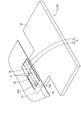
- FIG. 1 Perspective view of power storage module according to Embodiment 1.
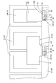
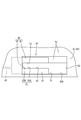
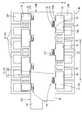
- Top view of power storage module Partially enlarged plan view showing a state in which a protrusion of a conductive member is connected to a land of a flexible printed circuit board 3 is a sectional view taken along line AA of FIG.
- Plan view of flexible printed circuit board Main part enlarged plan view of FIG.
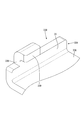
- Perspective view of conductive member Plan view of conductive member
- the top view showing the state where the projection of the conductive member was inserted in the insertion opening.
- the top view which shows the state in which the protrusion of the conductive member entered the entrance opening.
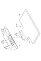
- the perspective view showing the state before the projection of the conductive member is inserted in the insertion opening.
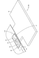
- FIG. 1 The perspective view which shows the state in which the protrusion of the conductive member was inserted in the insertion opening.
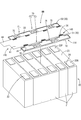
- Top view of power storage module Side view with some power storage modules omitted A perspective view showing a state before a wiring module is attached to a storage element group.
- Top view of wiring module A perspective view showing a state before attaching a flexible printed circuit board to a conductive member.
- FIG. 22 is a sectional view taken along line BB of FIG. The perspective view which omitted some conductive members concerning Embodiment 4.
- 25 is a sectional view taken along line CC in FIG.
- the power storage module M of the present embodiment is a power storage module M used as a drive source of a vehicle such as an electric vehicle or a hybrid vehicle, and includes a power storage element group 20 in which a plurality of power storage elements 21 are arranged; A plurality of conductive members 30 having a main body 33 connected to the electrode terminals 22 and a flexible printed circuit board (hereinafter, also simply referred to as “FPC”) 40 having a plurality of conductive paths 42 to which the conductive members 30 are connected are provided. It is configured.
- the conductive member 30 and the flexible printed board 40 correspond to a wiring member.
- the front-rear direction refers to the left-right direction in FIGS. 2 and 6, with the F side being the front side and the B side being the rear side.
- the left and right directions are described with reference to the up and down directions in FIGS. 2 and 6, the L side being the left side, and the R side being the right side.
- the storage element 21 is, for example, a rectangular parallelepiped secondary battery having a flat outer shape. As illustrated in FIGS. 1 and 2, a plurality (six in the present embodiment) of storage elements 21 are stacked in the front-rear direction.
- the power storage element group 20 is arranged in a line in such a way that
- the energy storage device 21 has an electrode arrangement surface (upper surface in FIG. 1) 23 perpendicular to a surface facing the adjacent energy storage device 21. Electrode terminals 22 are arranged. One of the pair of electrode terminals 22 is a positive terminal 22P, and the other is a negative terminal 22N. Two adjacent storage elements 21 in the storage element group 20 are connected such that electrode terminals 22 having different polarities are adjacent to each other (a positive terminal 22P of one storage element 21 and a negative terminal of another storage element 21 adjacent thereto). 22N are arranged in a line in the front-rear direction (so that they are adjacent to each other).
- the conductive member 30 is formed by processing a conductive metal plate such as copper, copper alloy, aluminum, aluminum alloy, and stainless steel (SUS) by pressing or the like.
- a conductive metal plate such as copper, copper alloy, aluminum, aluminum alloy, and stainless steel (SUS) by pressing or the like.
- the conductive member 30 includes a connection bus bar 31 that connects the positive terminal 22P and the negative terminal 22N of the adjacent storage element 21 in the storage element group 20 and an end portion of the storage element group 20. And an end bus bar 32 connected to the arranged electrode terminals 22.
- connection bus bar 31 includes a substantially rectangular flat main body 33 that is long in the front-rear direction, and a connection protrusion 34 that is continuously provided on one side edge of the main body 33 in the left-right direction. It is provided with.
- the end bus bar 32 has a length in the front-rear direction of the main body 33 shorter than that of the connection bus bar 31, but the other configuration is the same, and thus the description is omitted.
- the main body 33 is electrically connected to the electrode terminals 22 of the power storage device 21 by welding or the like, and connects adjacent power storage devices 21 in series as shown in FIGS. 1 and 2. Therefore, in the present embodiment, by connecting the electrode terminals 22 of different polarities of the adjacent power storage elements 21 to each other by the connection bus bar 31, the plurality of power storage elements 21 are connected in series to form the power storage element group 20. I have. Note that, in the power storage element group, some of the power storage elements in the power storage element group are arranged so that the electrode terminals of the same polarity are adjacent to each other, so that some of the power storage elements in the power storage element group are connected in parallel. May be configured.
- each conductive member 30 is arranged such that a connection protrusion 34 described later is positioned at a central side edge of the power storage element 21, and the power storage element 21
- the electrodes are arranged on the electrode terminals 22 so as to be linearly arranged in the front-back direction.
- the main body 33 has an extension 33A that extends laterally at a substantially central portion in the front-rear direction on one side edge in the left-right direction, and a connection protrusion is provided at an extension end edge of the extension 33A. 34 are protruded.
- connection protrusion 34 has a rectangular flat plate portion 35 slightly projecting perpendicularly to the plate surface of the main body portion 33, and a flat plate portion 35.
- connection protrusion 36 is formed in a rectangular parallelepiped shape shorter in the front-rear direction than the flat plate portion 35.
- the FPC 40 is a member for electrically connecting the plurality of conductive members 30 to an electronic control unit (hereinafter, also referred to as “ECU”) (not shown) and transmitting a voltage applied to the conductive members 30 to the ECU.
- ECU electronice control unit
- the FPC 40 has a substantially rectangular sheet-shaped FPC main body 41 that is long in the front-rear direction along the storage element 21.
- the FPC main body 41 includes a plurality of conductive paths 42 formed of copper foil, and an insulating resin film 43 covering both surfaces of the conductive paths 42.
- an external connection portion 44 protruding forward in a substantially rectangular shape is provided at a front end portion of the FPC main body 41.
- front ends which are one ends of the plurality of conductive paths 42, are integrated, and each of the conductive paths 42 is connected to the ECU via the external connection portion 44. I have.
- a plurality of joints 45 to which the conductive member 30 is connected are formed on both side edges in the left-right direction of the FPC main body 41 so as to be linearly arranged in the direction in which the FPC main body 41 extends.
- the joining portion 45 has a substantially rectangular shape that is long in the front-rear direction, and includes an insertion opening 50 that penetrates the FPC body 41 in the thickness direction, and a plurality of conductive paths 42. And a land 60 formed by exposing a rear end portion, which is the other end portion, to an upper side opposite to the power storage element 21 side.
- the insertion opening 50 is an opening formed by a series of opening edges 50 ⁇ / b> A, and the connection protrusion 36 of the conductive member 30 can be inserted into the insertion opening 50 from below the power storage element 21.
- the insertion opening 50 is composed of an insertion opening 51 arranged at the rear end of the joint 45 and an entry opening 52 communicating with the front of the insertion opening 51.
- the insertion opening 51 is formed in a substantially rectangular shape in a plan view larger than the outer shape of the connection protrusion 36 of the conductive member 30, and is inserted into the insertion opening 51 with the connection protrusion 36 as shown in FIG. 10.
- the connection projection 36 is inserted with a gap between the connection opening 51 and the edge 51A (around the connection projection 36).
- the entrance opening 52 has a shape that is long in the front-rear direction, which is the direction in which the conductive members 30 are arranged.
- the entry opening 52 is formed at the front end of the insertion opening 51 and extends forward from a position near the center of the FPC main body 41.
- the length L1 of the entrance opening 52 in the front-rear direction is larger than the length L2 of the insertion opening 51 in the front-rear direction, and the connection protrusion of the conductive member 30 adjacent to the power storage element group 20 in the front-rear direction is connected to the storage element group 20.
- the sum of the maximum tolerance dimension of the gap between the parts 36 in the front-back direction (the sum of the maximum value of the manufacturing tolerance and the maximum value of the assembly tolerance between the connection projections 36) L3 and the length dimension L4 of the connection projection 36 in the front-rear direction. (L1 ⁇ L3 + L4).
- An opening width L5 in the left-right direction (orthogonal direction) orthogonal to the direction in which the entry opening 52 extends is substantially the same as the length L6 in the left-right direction of the connection protrusion 36 of the conductive member 30.
- the connection protrusion 36 of the conductive member 30 inserted into the insertion opening 51 can enter in an adapted state.
- connection protrusion 36 can be easily inserted into the insertion opening 50 as shown in FIGS.
- the connection protrusion 36 By sliding the FPC 40 backward with the connection protrusion 36 inserted through the opening 51, the connection protrusion 36 enters in a state adapted to the entry opening 52. That is, as shown in FIGS. 11 and 14, when the connection projection 36 enters the entry opening 52 of the joining portion 45, the side edges 53 ⁇ / b> A on both sides of the entry opening 52 in the left-right direction and the connection projection 36 are connected in the left-right direction , The pair of side edge lands 61 can be prevented from being displaced in the left-right direction with respect to the connection protrusion 36.
- the FPC 40 is moved rearward with the connection projections 36 inserted through the insertion openings 51.
- the connecting projections 36 can enter all the entrance openings 52 at once.
- the land 60 is provided at the edge 53 of the entrance opening 52, and a pair of sides disposed on the left and right side edges 53A of the entrance opening 52. It is configured to include an edge land 61 and a connection land 62 arranged at a front edge 53 ⁇ / b> B of the entrance opening 52.
- the pair of side edge lands 61 is formed to extend in the front-rear direction in which the entrance opening 52 extends along the side edge 53A of the entrance opening 52, and is formed over the entire length of the side edge 53A in the front-rear direction. I have.
- connection land 62 connects the pair of side edge lands 61 in the left-right direction along the front edge of the entrance opening 52, and the conductive path 42 extends forward from the front end of the connection land 62.
- the length L1 of the entrance opening 52 in the front-rear direction is the maximum tolerance dimension L3 between the connection protrusions 36 of the adjacent conductive members 30 and the length L1 of the connection protrusion 36 in the front-rear direction. Since the FPC 40 is formed to be larger than the sum of the length L4 and the FPC 40 is slid rearward and the connection projection 36 enters the entry opening 52 of the joint 45, the connection projection 36 is inserted into the entry opening 52.
- the connection protrusion 36 is always disposed between the pair of side edge lands 61 without protruding. Accordingly, the pair of side edge lands 61 and the connection protrusion 36 can be easily and reliably connected by the solder P or the like.
- the present embodiment is configured as described above. Next, the method of manufacturing the power storage module M will be described, and the operation and effects of the flexible printed circuit board 40 will be described.
- a plurality of conductive members 30 are arranged so as to connect electrode terminals 22 having different polarities in adjacent storage elements 21 of storage element group 20.
- each conductive member 30 is arranged such that the connection protrusion 34 of each conductive member 30 is located on the center side of the power storage element 21. Further, main body portions 33 of respective conductive members 30 are arranged so as to be linearly aligned in the front-back direction in which power storage elements 21 are arranged.
- the conductive member 30 disposed on the electrode terminal 22 and the electrode terminal 22 are electrically connected by welding or the like to form a power storage element group 20 in which adjacent power storage elements 21 are connected in series.
- the bonding portion 45 of the FPC 40 is aligned with the conductive member 30, and the connection protrusion 36 of the conductive member 30 and the land 60 of the bonding portion 45 are connected by solder P.
- the plate-shaped connection portion provided on the conductive member is placed on a land formed by exposing the conductive path in the FPC and soldering is performed, the plate-shaped connection portion and the land are connected to each other. Since there is a possibility of displacement, a positioning means such as a positioning jig is required separately.
- the FPC 40 of the present embodiment is formed with a plurality of connecting protrusions 36 that are formed to be larger than the outer shape of the connecting protrusion 36 so that the connecting protrusion 36 can be inserted with a gap around the connecting protrusion 36.
- the flexible printed circuit board 40 in a form narrower than the insertion openings 51 so that the insertion openings 51 and the connection projections 36 are provided so as to be able to enter from the insertion openings 51.
- the conductive path 42 has a land 60 to which the connection protrusion 36 is connected to the edge 53 of the entrance opening 52.
- the connection protrusion 36 fits into the entry opening 52 and enters. Then, the pair of side edges 53A of the entry opening 52 and the connection projection 36 are locked in the left-right direction, so that the connection projection 36 of the conductive member 30 is displaced in the left-right direction with respect to the entry opening 52.
- the connection protrusion 36 can be easily positioned with respect to the pair of side edge lands 61.
- connection protrusion 36 is inserted into the insertion opening 51 larger than the outer shape of the connection protrusion 36 of the conductive member 30, and the connection protrusion 36 is inserted in a state where the connection protrusion 36 fits into the entry opening 52 narrower than the insertion opening 51. Therefore, for example, compared to the case where a plate-shaped connecting portion is arranged on a land, even after the connecting protrusion 36 is arranged between the pair of side edge lands 61, the pair of side edge lands 61 The detachment of the connection protrusion 36 from between can be suppressed.
- connection protrusion 36 and the pair of side edge lands 61 are reliably connected by the solder P, and the electric module can be completed.
- the flexible member having the plurality of conductive paths 42 to which the connection protrusions 36 of the connection protrusions 34 provided on the conductive member 30 connected to the electrode terminals 22 of the power storage element 21 are connected.
- a plurality of insertion openings 51 which are formed on the printed circuit board 40 and are larger than the outer shape of the connection protrusion 36 and through which the connection protrusion 36 can be inserted with a gap around the connection protrusion 36;
- a plurality of entry openings 52 that are provided corresponding to the respective insertion openings 51 so as to be able to enter from the insertion openings 51 and that extend in the plate surface direction of the flexible printed circuit board 40 in a form narrower than the insertion openings 51;
- the conductive path 42 has a land 60 where the connection protrusion 36 is connected to the edge 53 of the entrance opening 52.
- the present embodiment includes a plurality of conductive members 30 having a main body 33 connected to the electrode terminals 22 of the power storage element 21, a flexible printed board 40 having a plurality of conductive paths 42 to which the conductive members 30 can be connected,
- the conductive member 30 has a connection protrusion 34 protruding from the main body 33, and the flexible printed circuit board 40 is formed to be larger than the outer shape of the connection protrusion 36 of the connection protrusion 34.
- a plurality of insertion openings 51 through which the connection protrusions 36 can be inserted with a gap around the protrusions 36, and the connection protrusions 36 correspond to the respective insertion openings 51 so as to be able to enter from the insertion openings 51.
- a plurality of entrance openings 52 extending in the direction of the surface of the flexible printed circuit board 40 in a form narrower than the insertion opening 51.
- the conductive path 42 has an edge 53 of each entrance opening 52.
- Connect to Part 36 has a land 60 that can be connected.
- connection protrusion 36 of the conductive member 30 when the connection protrusion 36 of the conductive member 30 is inserted through the insertion opening 51 and the flexible printed circuit board 40 is slid backward to cause the connection protrusion 36 to enter the entry opening 52,
- the lateral projection 53A which is orthogonal to the direction in which the 52 extends, and the connection projection 36 are locked in the left-right direction, and the connection projection 36 of the conductive member 30 is easily positioned with respect to the land 60 of the flexible printed circuit board 40. can do.
- the land 60 and the connection protrusion 36 can be easily connected by the solder P or the like.
- connection protrusion 36 is inserted into the insertion opening 51 which is larger than the outer shape of the connection protrusion 36 of the conductive member 30, the connection protrusion 36 enters the entrance opening 52 which is narrower than the insertion opening 51.
- the connection protrusion 36 is inserted into the insertion opening 51 which is larger than the outer shape of the connection protrusion 36 of the conductive member 30.
- the entry opening 52 extends forward from the insertion opening 51 in the same direction so that the extending directions of the plurality of entry openings 52 all match.
- the connection protrusions 36 are inserted through the plurality of insertion openings 51 and the entire flexible printed circuit board 40 is slid rearward, whereby the connection protrusions 36 enter the respective entry openings 52 at a time and are positioned. be able to.
- connection protrusion 36 and the land 60 can be connected.
- the length L1 in the front-rear direction in which the land 60 extends is set to be larger than the sum of the maximum tolerance dimension L3 between the adjacent connection protrusions 36 and the length L4 in the front-rear direction of the connection protrusion 36. I have.
- the length L1 in the front-rear direction in which the land 60 extends is the sum of the maximum tolerance dimension L3 between the connection protrusions 36 of the plurality of conductive members 30 and the length L4 in the front-rear direction of the connection protrusion 36. It is set larger than.
- the length dimension L1 of the land 60 in the front-rear direction is the maximum tolerance dimension L3 of the plurality of conductive members 30 in the alignment direction of the connection protrusions 36 and the length of the connection protrusions 36 in the front-rear direction. Since it is larger than the sum of the dimensions L4, for example, even if the gap dimension in the front-rear direction, which is the alignment direction of the plurality of conductive members 30, varies due to assembly tolerance or manufacturing tolerance, each of the connection protrusions It is possible to suppress displacement between the land 36 and the land 60. Thereby, the land 60 and the connection protrusion 36 can be reliably connected.
- the insertion opening 50 formed by the entry opening 52 and the insertion opening 51 is an opening in which the opening edges 50A are continuously connected.
- the opening edges 50A of the insertion openings 50 are continuously connected, it is possible to suppress a decrease in the strength of the opening edges 50A of the insertion openings 50.
- the opening width L5 in the left-right direction of the entry opening 52 is the same as the length L6 in the left-right direction of the connection protrusion 36, the connection protrusion 36 and the land 60 are soldered to each other. Can be easily connected.
- the opening width L5 of the entrance opening 52 and the length L6 in the left-right direction of the connection projection 36 are the same when the opening width L5 of the entrance opening 52 in the left-right direction of the connection projection 36 is the same. This includes the case where the length L6 is set slightly larger than the length L6, and the case where the opening width L5 of the entrance opening 52 is set slightly smaller than the length L6 of the connection protrusion 36 in the left-right direction. .
- the power storage module M1 according to the second embodiment includes an alignment member 70 that aligns and holds the conductive member 30 according to the first embodiment, and the length L1 of the entrance opening 52 in the FPC 40 in the front-rear direction is changed. Since the functions and effects common to the first embodiment are duplicated, description thereof may be omitted. Further, the same reference numerals are used for the same configuration as the first embodiment.
- the power storage module M1 includes a power storage element group 20 in which a plurality of power storage elements 21 are arranged, and a wiring module WM attached to the electrode arrangement surface 23 of the power storage element group 20.
- the wiring module WM includes a plurality of conductive members 30 having a main body 33 connected to the electrode terminals 22 of the power storage element 21, an FPC 140 having a plurality of conductive paths 42 to which the conductive members 30 are connected, and a plurality of conductive members 30. And an alignment member 70 that linearly aligns and holds the power storage elements 21 in the front-rear direction, which is the direction in which the power storage elements 21 are arranged.
- the power storage module M1 of the present embodiment integrates the plurality of conductive members 30, the FPC 140, and the alignment member 70 into one wiring module WM, and then places the wiring module WM on the electrode arrangement surface 23 of the power storage element group 20. It is configured to be attached. Note that the storage element group 20 and the conductive member 30 have the same configurations as those in the first embodiment, and therefore, individual descriptions are omitted.
- the alignment member 70 is formed of an insulating resin, and includes a pair of holding members 71 attached from above to the electrode arrangement surface 23 of the power storage element group 20, as shown in FIG.
- each of the pair of holding members 71 is formed in a substantially rectangular flat plate shape that is long in the front-rear direction in which the power storage elements 21 are arranged.
- the holding member 71 that linearly aligns and holds the conductive members 30 that connect the electrode terminals 22 on the right side of the power storage element 21 in the front-rear direction is a first holding member (“first alignment”).
- first alignment An example of the “member” is 71R
- second holding member of the “second alignment member”.
- 71L One example
- the lower ends of the first holding member 71 ⁇ / b> R and the second holding member 71 ⁇ / b> L are fitted from above into fitting recesses 24 provided between the electrode terminals 22 of the power storage elements 21 adjacent in the front-back direction in the power storage element group 20.
- a collision portion 72 is provided.
- first holding member 71 ⁇ / b> R is arranged on electrode terminal 22 at the right end of power storage element group 20 such that fitting protrusion 72 is fitted into fitting recess 24.
- the second holding member 71L is arranged on the electrode terminal 22 at the left end of the power storage element group 20 such that the fitting protrusion 72 is fitted into the fitting recess 24.
- a plurality of housing portions 74 in which the conductive members 30 are housed in a line in the front-rear direction are provided on the upper portions of the first holding member 71R and the second holding member 71L. It is provided through.
- three housing portions 74 in the front-rear direction are connected in a line in the front-rear direction by two connection portions 75.
- Each of the housing portions 74 has a substantially rectangular opening in a plan view at the lower side which is the storage element 21 side and the upper side which is the opposite side to the storage element 21 side, and a part of the central wall 74A of the storage element 21. Has a central opening 76 that is open.
- the main body 33 of the conductive member 30 is adapted to be accommodated from above in the accommodating portion 74, and when the main body 33 is accommodated in the accommodating portion 74, the connection protrusion 34 is moved to the central opening 76. To fit.
- the main body 33 is stored in the housing 74, the main body 33 is supported from below by a support (not shown) provided at the lower end of the housing 74.
- the conductive member 30 moves in the front-rear direction at both left and right ends of the power storage element group 20.
- the connecting protrusions 36 of the connecting protrusions 34 of the conductive member 30 are arranged in a straight line in the front-rear direction.
- the FPC 140 has a length L21 in the front-rear direction of the entrance opening 152 at the joint 145 different from that of the first embodiment, but the other configuration is the same.
- the length L21 in the front-rear direction of the entrance opening 152 is connected to the maximum tolerance dimension L23 in the front-rear direction between the first holding member 71R and the second holding member 71L when the alignment member 70 is attached to the power storage element group 20. It is set to be larger than the sum of the length dimension L4 of the protrusion 36 in the front-rear direction (L21 ⁇ L23 + L4).
- the wiring module WM of the present embodiment has the above-described configuration. Next, a method for manufacturing the wiring module WM will be described, and then a method for manufacturing the power storage module M1 will be described.
- the main body portion 33 of the conductive member 30 is housed from above in all the housing portions 74 of the first holding member 71R and the second holding member 71L of the alignment member 70, and the plurality of conductive members 30 are linearly arranged in the front-rear direction. Constitute a pair of holding members 71 aligned.
- the distance between the first holding member 71R and the second holding member 71L is substantially equal to the distance between the pair of electrode terminals 22 of the power storage element 21, and the first holding member 71R and the second The pair of holding members 71 are arranged such that the fitting protrusion 72 of the holding member 71L can be fitted into the fitting recess 24 of the power storage element group 20.
- connection projection 36 inserted into the insertion opening 51 enters into a state adapted to the entrance opening 152.
- the left and right side edges 53A of the entrance opening 152 and the connection protrusions 36 are locked in the left and right direction, so that the connection protrusions 36 of the conductive member 30 with respect to the pair of side edge lands 61 of the lands 60 of the FPC 140.
- the longitudinal dimension L21 of the entrance opening 152 in the front-rear direction is the maximum tolerance dimension L23 in the front-rear direction between the first holding member 71R and the second holding member 71L, and the front-rear direction of the connection protrusion 36.
- connection protrusion 36 of the conductive member 30 and the pair of side edge lands 61 of the flexible printed circuit board 40 are positioned, the connection protrusion 36 and the pair of side edge lands 61 are connected by solder P.
- the wiring module WM in which is integrated is completed.
- the wiring module WM When the wiring module WM is completed, the wiring module WM is assembled to the electrode arrangement surface 23 of the power storage element group 20 so that the fitting projection 72 of the alignment member 70 is fitted into the fitting recess 24 of the power storage element group 20. 15 and 17, the main body 33 of the conductive member 30 and the electrode terminal 22 of the power storage element 21 are welded to complete the power storage module M1.
- the present embodiment is a wiring module WM attached to a power storage element group 20 in which a plurality of power storage elements 21 having a pair of electrode terminals 22 are arranged, and is connected to the electrode terminals 22 of the power storage element 21.
- a plurality of conductive members 30 having a main body 33, a plurality of conductive members 30 having connection protrusions 34 protruding from the main body 33, a flexible printed circuit board 40 having a plurality of conductive paths 42 to which the conductive members 30 are connected, and a plurality of conductive members
- an alignment member 70 that aligns and holds the power storage elements 30 in the front-rear direction, which is the direction in which the power storage elements 21 are arranged.
- the flexible printed circuit board 40 is formed to be larger than the outer shape of the connection protrusion 36 of the connection protrusion 34.
- the conductive path 42 is connected to the edge 53 of the entrance opening 152 by a connection projection.
- 36 has a land 60 to which it is connected.
- each entrance opening 152 extends forward from the insertion opening 51 in the same direction so that the direction in which the plurality of entrance openings 152 extend and the direction in which the plurality of power storage elements 21 are aligned coincide with each other.
- the alignment member 70 includes a first holding member (first alignment member) 71R that aligns and holds the conductive member 30 that connects one of the pair of electrode terminals 22 to each other, and the other electrode terminal. And a second holding member (second alignment member) 71L that aligns and holds the conductive members 30 connecting the two 22.
- the pair of side edge lands 61 of the land 60 extends along the front-rear direction in which the entrance opening 152 extends.
- the length L21 extending in the extending direction in which the pair of side edge lands 61 extends is the front-rear direction between the first holding member (first alignment member) 71R and the second holding member (second alignment member) 71L. Is larger than the sum of the maximum tolerance dimension L23 and the length dimension L4 of the connecting protrusion 36 in the front-rear direction.
- connection protrusion 36 can be connected to the pair of side edge lands 61. In other words, it is possible to prevent the pair of side edge lands 61 from being displaced with respect to the connection protrusion 36 and being unable to be connected.
- the conductive member 230 according to the third embodiment is obtained by changing the shape of the connection protrusion 36 of the connection protrusion 34 of the conductive member 30 according to the first embodiment and changing the width L5 of the entrance opening 252 in the left-right direction. Since the configuration, operation, and effect common to the first embodiment are duplicated, description thereof will be omitted. Further, the same reference numerals are used for the same configuration as the first embodiment.
- connection protrusion 236 of the connection protrusion 234 of the conductive member 230 is provided with a notch groove 238 that extends in the front-rear direction at the lower end of the body 33.
- the notch groove 238 is formed to be slightly concave in an arc shape with respect to the connection protrusion 236, and is formed over the entire length of the connection protrusion 236 in the front-rear direction.
- connection protrusion 236 is inserted so that the side edge 53A of the entry opening 252 on the main body 33 side is fitted into the notch groove 238 as shown in FIG. From the entrance opening 51 into the entrance opening 252.
- connection protrusion 236 when the connection protrusion 236 enters the entry opening 252, the notch groove 238 and the side edge 53 A of the entry opening 252 on the main body 33 side are fitted in an uneven manner, so that the upper side edge of the notch groove 238.
- the engagement protrusion 238A of the FPC 240 and the side edge 53A of the entry opening 252 in the FPC 240 are locked in the vertical direction, which is the direction in which the connection projection 236 protrudes, so that the connection projection 236 extends upward from the entry opening 252. It is designed to be retained.
- the connection protrusion 236 of the conductive member 230 and the pair of side land lands 61 of the FPC 240 can be connected by the solder P without being displaced vertically and horizontally.
- the conductive member 330 according to the fourth embodiment is obtained by changing the shape of the connection protrusion 36 of the connection protrusion 34 of the conductive member 30 according to the first embodiment, and has the same configuration, operation, and effect as those of the first embodiment. The description is omitted because it overlaps. Further, the same reference numerals are used for the same configuration as the first embodiment.
- connection protrusion 336 of the connection protrusion 334 of the conductive member 330 has a projecting locking piece (a “engaging portion”) whose protruding end projects toward the main body 33. 339).
- the overhanging piece 339 is formed by, for example, beating the projecting end of the connection protrusion 336.
- the overhang dimension L37 of the overhanging piece 339 is substantially the same as the plate thickness of the connection protrusion 334. It has been.
- connection protrusion 336 of the conductive member 330 and the pair of side land lands 61 of the FPC 40 can be connected by the solder P without being displaced up, down, left, and right.
- the protruding portion is formed in a rectangular parallelepiped shape.
- the present invention is not limited to this, and the protrusion may be formed in a columnar shape or a polygonal column shape.
- the joining portion 45 connected to the connection protrusion 36 of the conductive member 30 connected to the right electrode terminal 22 of the power storage device 21 and the left electrode terminal 22 of the power storage device 21 are connected.
- Both the connecting protrusion 36 of the conductive member 30 and the joint 45 connected to the conductive member 30 are formed on the FPC 40.
- the present invention is not limited to this, and an FPC is provided in which the FPC body is separated in the left-right direction and a joint is provided that is connected to only the protrusion of the conductive member used as one of the electrode terminals in the left-right direction of the storage element. May be.
- the insertion opening 51 is formed in a substantially rectangular shape in plan view.
- the invention is not limited thereto, and the insertion opening may be formed in a circular shape or an elliptical shape in a plan view.
- the opening edge 50A of the insertion opening 50 is configured to be continuous.
- the configuration is not limited to this. If a metal plate or the like is attached to the surface of the joint portion on the side of the power storage element to reinforce it, the insertion opening is opened on the side of the FPC and the opening edges are not connected continuously. There may be.
Landscapes
- Chemical & Material Sciences (AREA)
- Chemical Kinetics & Catalysis (AREA)
- Electrochemistry (AREA)
- General Chemical & Material Sciences (AREA)
- Engineering & Computer Science (AREA)
- Manufacturing & Machinery (AREA)
- Microelectronics & Electronic Packaging (AREA)
- Connection Of Batteries Or Terminals (AREA)
- Battery Mounting, Suspending (AREA)
- Secondary Cells (AREA)
Abstract
本明細書によって開示されるフレキシブルプリント基板は、蓄電素子21の電極端子22に接続される導電部材30に突設された接続突片34の接続突部36が接続される複数の導電路42を有するフレキシブルプリント基板40であって、接続突部36の外形よりも大きく形成され、接続突部36の周りに隙間を有した状態で接続突部36が挿通可能な複数の差込開口51と、接続突部36が差込開口51から進入可能にそれぞれの差込開口51に対応して設けられ、差込開口51よりも狭い形態で延びる複数の進入開口52と、を有しており、導電路42は、進入開口52の縁部53に位置して接続突部36が接続されるランド60を有している構成とした。
Description
本明細書によって開示される技術は、フレキシブルプリント基板、配線部材、蓄電モジュールおよび接続モジュールに関する。
例えば、電池セル間の電圧を検出する電圧検出回路を備えた電池モジュールとして、特許第5621765号公報(特許文献1)に記載のものが知られている。この電池モジュールの電圧検出回路は、隣り合う電池セルの端子に接続される連結バスバに設けられた結線部材を、フレキシブルプリント基板(FPC)に形成されているコンタクトパッド上に配置し、結線部材とコンタクトパッドとがリフロー半田付けによって接続されて形成されている。
ところで、この種の電圧検出回路は、バスバに相当する導電部材に設けられた平板状の板状接続部を、FPCのコンタクトパッドに相当するランドに配置して半田付けを行うため、板状接続部とランドとが位置ずれすることを防ぐ位置決め治具などの位置決め手段が別途必要となってしまう。また、ランド上に板状接続部を正確に配置したとしても、ランドと板状接続部との接続時にフレキシブルプリント基板もしくは配線部材に位置ずれが生じてしまう虞がある。だからといって、位置ずれ対策として、ランドと板状接続部を個別に位置決めして接続すると作業が煩雑になってしまう。
本明細書では、フレキシブルプリント基板と導電部材とが位置ずれすることを容易に抑制し、フレキシブルプリント基板と導電部材との接続を容易にする技術を開示する。
本明細書によって開示される技術は、蓄電素子の電極端子に接続される導電部材に突設された突部が接続される複数の導電路を有するフレキシブルプリント基板であって、前記突部の外形よりも大きく形成され、前記突部の周りに隙間を有した状態で前記突部が挿通可能な複数の差込開口と、前記突部が前記差込開口から進入可能にそれぞれの前記差込開口に対応して設けられ、前記差込開口よりも狭い形態で前記フレキシブルプリント基板の板面方向に延びる複数の進入開口と、を有しており、前記導電路は、前記進入開口の縁部に位置して前記突部が接続されるランドを有している構成とした。
また、本明細書によって開示される技術は、配線部材であって、蓄電素子の電極端子に接続される本体部を有する複数の導電部材と、前記導電部材が接続可能な複数の導電路を有するフレキシブルプリント基板と、を備え、前記導電部材は、前記本体部に突設された突部を有しており、前記フレキシブルプリント基板は、前記突部の外形よりも大きく形成され、前記突部の周りに隙間を有した状態で前記突部が挿通可能な複数の差込開口と、前記突部が前記差込開口から進入可能にそれぞれの前記差込開口に対応して設けられ、前記差込開口よりも狭い形態で前記フレキシブルプリント基板の板面方向に延びる複数の進入開口と、を有しており、前記導電路は、それぞれの前記進入開口の縁部に位置して前記突部が接続可能なランドを有している構成とした。
また、本明細書によって開示される技術は、蓄電モジュールであって、複数の蓄電素子が並べられた蓄電素子群と、上記の配線部材とを備えている。
また、本明細書によって開示される技術は、一対の電極端子を有する複数の蓄電素子を並べた蓄電素子群に取り付けられる配線モジュールであって、前記蓄電素子の電極端子に接続される本体部と、前記本体部に突設された突部とを有する複数の導電部材と、前記導電部材が接続される複数の導電路を有するフレキシブルプリント基板と、前記複数の導電部材を前記蓄電素子の並び方向に整列させて保持する整列部材と、を備え、前記フレキシブルプリント基板は、前記突部の外形よりも大きく形成され、前記突部の周りに隙間を有した状態で前記突部が挿通可能な差込開口と、前記差込開口に挿通された前記突部が進入可能に前記差込開口に連通して設けられ、前記差込開口よりも狭い形態で前記フレキシブルプリント基板の板面方向に延びる進入開口と、を有しており、前記導電路は、前記進入開口の縁部に位置して前記突部が接続されるランドを有している構成とした。
このような構成によると、導電部材の突部の外形よりも大きい差込開口に突部を挿通させ、フレキシブルプリント基板をスライドさせて突部を差込開口よりも狭い進入開口に進入させてランドと突部とを位置決めすることができる。したがって、例えば、ランドに対して板状の接続部を配置する場合に比べて、ランドと突部との位置決めが容易であり、導電部材の突部に対して差込開口の縁部に設けられたランドを容易に組み付けることができる。
また、突部が進入開口に進入すると、進入開口の延びる方向と直交する直交方向の縁部と突部とが直交方向に係止することにより、ランドに対して導電部材の突部を容易に位置決めすることができる。また、例えば、ランドに対して板状の接続部を配置する場合に比べて、ランドと突部とを位置決めした後でも、ランドと突部とが位置ずれすることを抑制することができる。これにより、ランドと突部とを半田などによって容易に接続することができる。
本明細書によって開示される開示される技術は、以下の構成としてもよい。
前記進入開口は、前記複数の進入開口の延びる方向が全て一致するように前記差込開口から同一方向に延びている構成にしてもよい。
前記進入開口は、前記複数の進入開口の延びる方向が全て一致するように前記差込開口から同一方向に延びている構成にしてもよい。
また、前記複数の導電部材は、整列した状態で前記本体部が前記電極端子に接続されており、前記進入開口は、前記複数の進入開口の延びる方向と前記複数の導電部材の整列方向とが一致するように前記差込開口から他の前記進入開口と同一方向に延びている構成にしてもよい。
また、それぞれの前記進入開口は、前記複数の進入開口の延びる方向と前記複数の蓄電素子の並び方向とが一致するように前記差込開口から同一の方向に延びている構成としてもよい。
このような構成によると、複数の差込開口に突部を挿通させて、フレキシブルプリント基板を蓄電素子の並び方向にスライドさせることにより、それぞれの進入開口に一度に突部を進入させて位置決めすることができる。
このような構成によると、複数の差込開口に突部を挿通させて、フレキシブルプリント基板を蓄電素子の並び方向にスライドさせることにより、それぞれの進入開口に一度に突部を進入させて位置決めすることができる。
前記ランドは、前記進入開口が延びる方向に沿って延びている構成としてもよい。
このような構成によると、複数の差込開口に挿通される突部の一部や、複数の導電部材のうちの一部の導電部材が進入開口の延びる方向にずれている場合でも、突部とランドとを接続させることができる。つまり、突部に対してランドが位置ずれして接続できなくなることを抑制することができる。
このような構成によると、複数の差込開口に挿通される突部の一部や、複数の導電部材のうちの一部の導電部材が進入開口の延びる方向にずれている場合でも、突部とランドとを接続させることができる。つまり、突部に対してランドが位置ずれして接続できなくなることを抑制することができる。
前記ランドが延びる延出方向の長さ寸法は、隣り合う前記突部間の最大公差寸法と突部についての延出方向の長さ寸法との和よりも大きく設定されている構成してもよい。
このような構成によると、ランドが延びる方向の長さ寸法が、複数の差込開口に挿通されるそれぞれの突部間の進入開口の延びる方向の最大公差寸法よりも大きくなっているから、例えば、複数の差込開口に進入する突部間の隙間寸法に組み付け公差や製造公差に起因したばらつきがあった場合でも、それぞれの突部に対してランドが延出方向に位置ずれすることを抑制し、ランドと突部とを確実に接続することができる。
このような構成によると、ランドが延びる方向の長さ寸法が、複数の差込開口に挿通されるそれぞれの突部間の進入開口の延びる方向の最大公差寸法よりも大きくなっているから、例えば、複数の差込開口に進入する突部間の隙間寸法に組み付け公差や製造公差に起因したばらつきがあった場合でも、それぞれの突部に対してランドが延出方向に位置ずれすることを抑制し、ランドと突部とを確実に接続することができる。
前記ランドが延びる延出方向の長さ寸法は、前記複数の導電部材間の最大公差寸法と突部についての延出方向の長さ寸法との和よりも大きく設定されている構成としてもよい。
このような構成によると、ランドが延びる方向の長さ寸法が、複数の導電部材の整列方向の最大公差寸法よりも大きくなっているから、例えば、複数の導電部材の整列方向の隙間寸法に組み付け公差や製造公差に起因したばらつきがあった場合でも、各導電部材の突部に対してランドが位置ずれすることを抑制し、ランドと突部とを確実に接続することができる。
このような構成によると、ランドが延びる方向の長さ寸法が、複数の導電部材の整列方向の最大公差寸法よりも大きくなっているから、例えば、複数の導電部材の整列方向の隙間寸法に組み付け公差や製造公差に起因したばらつきがあった場合でも、各導電部材の突部に対してランドが位置ずれすることを抑制し、ランドと突部とを確実に接続することができる。
前記整列部材は、前記一対の電極端子のうちの一方の前記電極端子同士を接続する前記導電部材を整列させて保持する第1整列部材と、他方の前記電極端子同士を接続する前記導電部材を整列させて保持する第2整列部材とを含み、前記ランドが延びる延出方向の長さ寸法は、前記第1整列部材と前記第2整列部材間についての前記蓄電素子の並び方向の最大公差寸法と突部についての延出方向の長さ寸法との和よりも大きく設定されている構成とした。
このような構成によると、ランドが延びる方向の長さ寸法が、第1整列部材と第2整列部材間の最大公差寸法と突部の長さ寸法との和よりも大きくなっているから、第1整列部材に保持される導電部材の突部と第2整列部材に保持される導電部材の突部との間で、組み付け公差や製造公差に起因したばらつきがあった場合でも、導電部材の突部に対してランドが位置ずれすることを抑制し、ランドと突部とを確実に接続することができる。
前記進入開口と前記差込開口とによって構成される挿通開口は、開口縁が一続きに繋がった開口とされている構成としてもよい。
例えば、フレキシブルプリント基板の側部に開口して開口縁が一続きに繋がっていない挿通開口の場合、側部に開口した部分の強度が低下してしまう。すると、差込開口から進入開口に突部を進入させ難くなったり、進入開口に進入した突部が進入開口から離脱してしまったりすることが懸念される。
例えば、フレキシブルプリント基板の側部に開口して開口縁が一続きに繋がっていない挿通開口の場合、側部に開口した部分の強度が低下してしまう。すると、差込開口から進入開口に突部を進入させ難くなったり、進入開口に進入した突部が進入開口から離脱してしまったりすることが懸念される。
ところが、このような構成によると、挿通開口の開口縁が一続きに繋がっているから、挿通開口の縁部の強度が低下することを抑制することができる。これにより、差込開口から進入開口に突部を進入させ難くなったり、進入開口に進入した突部が進入開口から離脱したりすることを抑制することができる。
前記進入開口の前記延びる方向と直交する直交方向の開口幅は、前記突部の前記直交方向の長さ寸法と同一とされている構成としてもよい。
ここで、開口幅と突部の直交方向の長さ寸法とが同一とは、進入開口の開口幅が突部の長さ寸法よりも僅かに大きく設定されている場合と、進入開口の開口幅が突部の長さ寸法よりも僅かに小さく設定されている場合を含む。
ここで、開口幅と突部の直交方向の長さ寸法とが同一とは、進入開口の開口幅が突部の長さ寸法よりも僅かに大きく設定されている場合と、進入開口の開口幅が突部の長さ寸法よりも僅かに小さく設定されている場合を含む。
このような構成によると、導電部材の突部を進入開口の縁部に設けられたランドに対して近接して配置することができるから、突部とランドとを半田などによって接続し易くすることができる。
前記突部は、前記進入開口の縁部と凹凸嵌合して前記縁部と突出方向に係止可能な係合部を有している構成としてもよい。
このような構成によると、突部が進入開口に進入した際に、進入開口の縁部と係合部とが突出方向に係止することで進入開口から突部が突出方向に離脱することを防ぐことができる。つまり、突部に対してランドが位置ずれすることをさらに抑制し、ランドと突部とを確実に接続することができる。
このような構成によると、突部が進入開口に進入した際に、進入開口の縁部と係合部とが突出方向に係止することで進入開口から突部が突出方向に離脱することを防ぐことができる。つまり、突部に対してランドが位置ずれすることをさらに抑制し、ランドと突部とを確実に接続することができる。
本明細書によって開示される技術によれば、フレキシブルプリント基板と導電部材とが位置ずれすることを容易に抑制し、フレキシブルプリント基板と導電部材との接続を容易にすることができる。
<実施形態1>
本明細書に開示された技術における実施形態1について図1から図14を参照して説明する。
本明細書に開示された技術における実施形態1について図1から図14を参照して説明する。
本実施形態の蓄電モジュールMは、電気自動車やハイブリット自動車等の車両の駆動源として使用される蓄電モジュールMであって、複数の蓄電素子21が並べられた蓄電素子群20と、蓄電素子21の電極端子22に接続される本体部33を有する複数の導電部材30と、導電部材30が接続された複数の導電路42を有するフレキシブルプリント基板(以下、単に「FPC」ともいう)40とを備えて構成されている。ここで、導電部材30とフレキシブルプリント基板40とが配線部材に相当する。なお、以下の説明において、前後方向とは、図2および図6における左右方向を基準とし、F側を前側、B側を後側とする。また、左右方向とは、図2および図6における上下方向を基準とし、L側を左側、R側を右側として説明する。
蓄電素子21は、例えば、外形が扁平な直方体状の二次電池であって、図1および図2に示すように、複数個(本実施形態では6個)の蓄電素子21が前後方向に積層されるように一列に並べられて蓄電素子群20が構成されている。
蓄電素子21は、隣接する蓄電素子21と対向する面に対して垂直な電極配置面(図1の上面)23を有しており、電極配置面23の左右方向両端部には、一対の扁平な電極端子22が配置されている。一対の電極端子22のうち一方は正極端子22Pとされ、他方は負極端子22Nとされている。蓄電素子群20において隣り合う2つの蓄電素子21は、異なる極性の電極端子22が互いに隣り合うように(1つの蓄電素子21の正極端子22Pと、これと隣接する他の蓄電素子21の負極端子22Nとが互いに隣り合うように)前後方向に一列に並べられている。
導電部材30は、例えば、銅、銅合金、アルミニウム、アルミニウム合金、ステンレス鋼(SUS)などの導電性を有する金属板をプレスなどによって加工することにより形成されている。
導電部材30は、図1および図2に示すように、蓄電素子群20において隣り合う蓄電素子21の正極端子22Pと負極端子22Nとを接続する接続バスバ31と、蓄電素子群20の端部に配された電極端子22に接続される端部バスバ32とを含んでいる。
接続バスバ31は、図8および図9に示すように、前後方向に長い略矩形平板状の本体部33と、本体部33の左右方向の一側縁に連設された接続突片34とを備えて構成されている。なお、端部バスバ32は、本体部33の前後方向長さ寸法が、接続バスバ31に比べて短く形成されているものの、その他の構成は同じであるため、説明を省略する。
本体部33は、蓄電素子21の電極端子22に溶接などによって電気的に接続され、図1および図2に示すように、隣り合う蓄電素子21を直列に接続する。したがって、本実施形態は、隣り合う蓄電素子21の異なる極性の電極端子22が接続バスバ31によって互いに接続されることにより、複数の蓄電素子21が直列に接続されて蓄電素子群20が構成されている。なお、蓄電素子群は、蓄電素子群の一部の蓄電素子を、同一極性の電極端子が互いに隣り合うように配置することにより、蓄電素子群の一部の隣り合う蓄電素子が並列に接続された蓄電素子群を構成してもよい。
また、それぞれの導電部材30における本体部33は、図5に示すように、後述する接続突片34が蓄電素子21の中央側の側縁に位置するように配置されると共に、蓄電素子21が並ぶ前後方向に直線状に整列されて電極端子22上に配置されるようになっている。
また、本体部33は、左右方向の一側縁における前後方向略中央部に側方に延出された延出部33Aを有しており、延出部33Aの延出端縁に接続突片34が突設されている。
接続突片34は、図5、図8および図9に示すように、本体部33の板面に対して垂直方向に向かって僅かに突出する矩形平板状の平板部35と、平板部35の延出端部から更に垂直方向に突出する接続突部(「突部」の一例)36とを有している。
接続突部36は、平板部35よりも前後方向に短い直方体状に形成されている。
FPC40は、複数の導電部材30と図示しない電子制御ユニット(以下、「ECU」ともいう)とを電気的に接続し、導電部材30に印可される電圧をECUに伝えるための部材である。FPC40は、図1、図2および図6に示すように、蓄電素子21の並びに沿うように前後方向に長い略矩形状のシート状のFPC本体41を有している。
FPC本体41は、図12に示すように、銅箔によって形成された複数の導電路42と、導電路42の両面を被覆する絶縁樹脂フィルム43とを備えている。
FPC本体41の前端部には、図6に示すように、前方に向かって略矩形状に突出する外部接続部44が設けられている。外部接続部44には、複数の導電路42の一方の端部である前端部が集約されており、この外部接続部44を介してそれぞれの導電路42がECUに接続されるようになっている。
FPC本体41の左右方向の両側縁部には、導電部材30が接続される複数の接合部45がFPC本体41の延びる方向に直線状にそれぞれ並んで形成されている。
接合部45は、図6、図7および図12に示すように、前後方向に長い略矩形状をなしており、FPC本体41を板厚方向に貫通する挿通開口50と、複数の導電路42の他方の端部である後端部が蓄電素子21側とは反対側の上側に露出させて形成したランド60とによって構成されている。
挿通開口50は、開口縁50Aが一続きに繋がった開口とされており、挿通開口50には、蓄電素子21側である下方から導電部材30の接続突部36が挿通可能とされている。
挿通開口50は、接合部45の後端部に配された差込開口51と、差込開口51の前部に連通する進入開口52とによって構成されている。
差込開口51は、導電部材30の接続突部36の外形よりも大きな平面視略矩形状に形成されており、差込開口51には、図10に示すように、接続突部36と差込開口51の縁部51Aとの間に(接続突部36周りに)隙間を有した状態で接続突部36が挿通されるようになっている。
進入開口52は、図11に示すように、導電部材30の並び方向である前後方向に長い形態をなしている。また、進入開口52は、差込開口51の前端であって、FPC本体41の中央寄りの位置から前方に延びて形成されている。
進入開口52の前後方向の長さ寸法L1は、差込開口51の前後方向の長さ寸法L2よりも大きく、且つ、蓄電素子群20に接続された前後方向に隣り合う導電部材30の接続突部36間の前後方向の隙間の最大公差寸法(接続突部36間の製造公差の最大値と組み付け公差の最大値の和)L3と接続突部36の前後方向の長さ寸法L4との和よりも大きく設定されている(L1≧L3+L4)。
進入開口52の延びる方向と直交する左右方向(直交方向)の開口幅L5は、導電部材30の接続突部36の左右方向の長さ寸法L6とほぼ同一とされ、進入開口52には、差込開口51に挿通された導電部材30の接続突部36が適合した状態で進入可能とされている。
したがって、差込開口51に接続突部36を差し込むことによって、図10および図13に示すように、挿通開口50へ接続突部36を容易に挿通することができるようになっており、差込開口51に接続突部36が挿通された状態でFPC40を後方に向かってスライドさせることにより、接続突部36が進入開口52に適合した状態で進入するようになっている。
つまり、図11および図14に示すように、接合部45の進入開口52に接続突部36が進入すると、進入開口52の左右方向の両側の側縁部53Aと接続突部36とが左右方向に係止することにより、接続突部36に対して一対の側縁ランド61が左右方向に位置ずれすることを防止することができるようになっている。
つまり、図11および図14に示すように、接合部45の進入開口52に接続突部36が進入すると、進入開口52の左右方向の両側の側縁部53Aと接続突部36とが左右方向に係止することにより、接続突部36に対して一対の側縁ランド61が左右方向に位置ずれすることを防止することができるようになっている。
また、FPC本体41の全ての接合部45における進入開口52は、差込開口51の前端から前方に延びているから、各差込開口51に接続突部36が挿通された状態でFPC40を後方にスライドさせることにより、全ての進入開口52に接続突部36を一度に進入させることができるようになっている。
ランド60は、図6、図7および図12に示すように、進入開口52の縁部53に設けられており、進入開口52の左右方向の両側の側縁部53Aに配される一対の側縁ランド61と、進入開口52の前縁部53Bに配される連結ランド62とを備えて構成されている。
一対の側縁ランド61は、進入開口52の側縁部53Aに沿うように進入開口52が延びる前後方向に延びて形成されており、側縁部53Aの前後方向の全長に亘って形成されている。
連結ランド62は、進入開口52の前縁に沿うように一対の側縁ランド61を左右方向に連結しており、連結ランド62の前端から導電路42が前方に向かって延びている。
つまり、進入開口52の前後方向の長さ寸法L1が、図11および図14に示すように、隣り合う導電部材30の接続突部36間の最大公差寸法L3と接続突部36の前後方向の長さ寸法L4との和よりも大きく形成されているから、FPC40を後方に向かってスライドさせて接合部45の進入開口52に接続突部36を進入させると、接続突部36が進入開口52からはみ出さず、接続突部36が一対の側縁ランド61の間に必ず配置されるようになっている。これにより、一対の側縁ランド61と接続突部36とを半田Pなどによって容易、かつ確実に接続することができるようになっている。
本実施形態は、以上のような構成であって、続いて、蓄電モジュールMの製造方法について説明すると共に、フレキシブルプリント基板40の作用および効果について説明する。
まず、図5に示すように、蓄電素子群20の隣り合う蓄電素子21における異なる極性の電極端子22同士を連結するように複数の導電部材30を配置する。
ここで、各導電部材30は、それぞれの導電部材30の接続突片34が、蓄電素子21の中央側に位置するように配置する。また、それぞれの導電部材30の本体部33が、蓄電素子21が並ぶ前後方向に直線状に整列されるように配置する。
次に、電極端子22上に配された導電部材30と電極端子22とを溶接などによって電気的に接続し、隣り合う蓄電素子21が直列に接続された蓄電素子群20を構成する。
次に、FPC40の接合部45を導電部材30に対して位置合わせし、導電部材30の接続突部36と接合部45のランド60とを半田Pによって接続する。
ここで、例えば、導電部材に設けられた平板状の板状接続部を、FPCにおいて導電路を露出させて形成したランド上に配置して半田付けを行う場合、板状接続部とランドとが位置ずれする虞があるため、位置決め治具などの位置決め手段が別途必要となってしまう。
また、ランド上に板状接続部を正確に配置したとしても、ランドと板状接続部との接続時にFPCもしくは配線部材に位置ずれが生じてしまう虞がある。位置ずれ対策として、ランドと板状接続部を個別に位置決めして接続すると作業が煩雑になってしまう。
ところが、本実施形態のFPC40は、図11に示すように、接続突部36の外形よりも大きく形成され、接続突部36の周りに隙間を有した状態で接続突部36が挿通可能な複数の差込開口51と、接続突部36が差込開口51から進入可能にそれぞれの差込開口51に対応して設けられ、差込開口51よりも狭い形態でフレキシブルプリント基板40の板面方向に延びる複数の進入開口52と、を有しており、導電路42は、進入開口52の縁部53に接続突部36が接続されるランド60を有している。
したがって、本実施形態によると、図10、図11、図13および図14に示すように、FPC40のそれぞれの接合部45における差込開口51に、蓄電素子群20に取り付けられた複数の導電部材30のそれぞれの接続突部36を挿通させ、フレキシブルプリント基板40を後方にスライドさせると、接続突部36が進入開口52に適合して進入する。すると、進入開口52の一対の側縁部53Aと接続突部36とが左右方向に係止することにより進入開口52に対して導電部材30の接続突部36が左右方向に位置ずれすることが防止され、一対の側縁ランド61に対して接続突部36を容易に位置決めすることができる。
また、導電部材30の接続突部36の外形よりも大きい差込開口51に接続突部36を挿通させて、差込開口51よりも狭い進入開口52に接続突部36を適合した状態で進入させているから、例えば、ランドに対して板状の接続部を配置する場合に比べて、一対の側縁ランド61の間に接続突部36を配置した後でも、一対の側縁ランド61の間から接続突部36が離脱することを抑制することができる。
これにより、接続突部36と一対の側縁ランド61とが確実に半田Pによって接続され、電モジュールを完成させることができる。
以上のように、本実施形態は、蓄電素子21の電極端子22に接続される導電部材30に突設された接続突片34の接続突部36が接続される複数の導電路42を有するフレキシブルプリント基板40であって、接続突部36の外形よりも大きく形成され、接続突部36の周りに隙間を有した状態で接続突部36が挿通可能な複数の差込開口51と、接続突部36が差込開口51から進入可能にそれぞれの差込開口51に対応して設けられ、差込開口51よりも狭い形態でフレキシブルプリント基板40の板面方向に延びる複数の進入開口52と、を有しており、導電路42は、進入開口52の縁部53に接続突部36が接続されるランド60を有している。
また、本実施形態は、蓄電素子21の電極端子22に接続される本体部33を有する複数の導電部材30と、導電部材30が接続可能な複数の導電路42を有するフレキシブルプリント基板40と、を備え、導電部材30は、本体部33に突設された接続突片34を有しており、フレキシブルプリント基板40は、接続突片34の接続突部36の外形よりも大きく形成され、接続突部36の周りに隙間を有した状態で接続突部36が挿通可能な複数の差込開口51と、接続突部36が差込開口51から進入可能にそれぞれの差込開口51に対応して設けられ、差込開口51よりも狭い形態でフレキシブルプリント基板40の板面方向に延びる複数の進入開口52と、を有しており、導電路42は、それぞれの進入開口52の縁部53に接続突部36が接続可能なランド60を有している。
すなわち、本実施形態によると、差込開口51に導電部材30の接続突部36を挿通させ、フレキシブルプリント基板40を後方にスライドさせて接続突部36を進入開口52に進入させると、進入開口52の延びる方向と直交する左右方向の側縁部53Aと接続突部36とが左右方向に係止してフレキシブルプリント基板40のランド60に対して導電部材30の接続突部36を容易に位置決めすることができる。これにより、ランド60と接続突部36とを半田Pなどによって容易に接続することができる。
また、導電部材30の接続突部36の外形よりも大きい差込開口51に接続突部36を挿通させて、差込開口51よりも狭い進入開口52に接続突部36を進入させているから、例えば、ランドに対して板状の接続部を配置する場合に比べて、ランド60と接続突部36とを位置決めした後でも、ランド60と接続突部36とが位置ずれすることを抑制することができる。
また、進入開口52は、複数の進入開口52の延びる方向が全て一致するように差込開口51から同一方向である前方に向かって延びている。これにより、複数の差込開口51に接続突部36を挿通させて、フレキシブルプリント基板40全体を後方にスライドさせることにより、それぞれの進入開口52に一度に接続突部36を進入させて位置決めすることができる。
また、ランド60における一対の側縁ランド61は、進入開口52が延びる延出方向である前後方向に沿って延びているから、複数の差込開口51に挿通される接続突部36の一部が前後方向に僅かにずれる場合でも、接続突部36とランド60とを接続させることができる。
つまり、接続突部36に対してランド60が位置ずれして接続できなくなることをさらに抑制することができる。
また、ランド60が延びる前後方向の長さ寸法L1は、隣り合う接続突部36間の最大公差寸法L3と接続突部36についての前後方向の長さ寸法L4との和よりも大きく設定されている。
詳細には、ランド60が延びる前後方向の長さ寸法L1は、複数の導電部材30の接続突部36間の最大公差寸法L3と接続突部36についての前後方向の長さ寸法L4との和よりも大きく設定されている。
つまり、このような構成によると、ランド60の前後方向の長さ寸法L1が、複数の導電部材30における接続突部36の整列方向の最大公差寸法L3と接続突部36の前後方向の長さ寸法L4の和よりも大きくなっているから、例えば、複数の導電部材30の整列方向である前後方向の隙間寸法に組み付け公差や製造公差に起因したばらつきがあった場合でも、それぞれの接続突部36とランド60とが位置ずれすることを抑制することができる。これにより、ランド60と接続突部36とを確実に接続することができる。
また、本実施形態によると、進入開口52と差込開口51とによって構成される挿通開口50は、開口縁50Aが一続きに繋がった開口とされている。
例えば、フレキシブルプリント基板の側部に開口して開口縁が一続きに繋がっていない挿通開口の場合、側部に開口した部分の強度が低下することにより、差込開口から進入開口に突部を進入させ難くなったり、進入開口に進入した突部が進入開口から離脱してしまったりすることが懸念される。
ところが、本実施形態によると、挿通開口50の開口縁50Aが一続きに繋がっているから、挿通開口50の開口縁50Aの強度が低下することを抑制することができる。これにより、差込開口51から進入開口52に接続突部36を進入させ難くなったり、進入開口52に進入した接続突部36が進入開口52から離脱し易くなったりすることを抑制することができる。
また、本実施形態は、進入開口52の左右方向の開口幅L5が、接続突部36の左右方向の長さ寸法L6と同一とされているから、接続突部36とランド60とを半田Pなどで容易に接続することができる。なお、ここに記載している進入開口52の開口幅L5と接続突部36の左右方向の長さ寸法L6とが同一とは、進入開口52の開口幅L5が接続突部36の左右方向の長さ寸法L6よりも僅かに大きく設定されている場合と、進入開口52の開口幅L5が接続突部36の左右方向の長さ寸法L6よりも僅かに小さく設定されている場合を含んでいる。
<実施形態2>
次に、実施形態2について図15から図20を参照して説明する。
次に、実施形態2について図15から図20を参照して説明する。
実施形態2の蓄電モジュールM1は、実施形態1における導電部材30を整列して保持する整列部材70を備えると共に、FPC40における進入開口52の前後方向の長さ寸法L1が変更されたものであって、実施形態1と共通する作用、および効果については重複するため、その説明を省略する場合がある。また、実施形態1と同じ構成については同一の符号を用いるものとする。
実施形態2の蓄電モジュールM1は、複数の蓄電素子21が並べられた蓄電素子群20と、蓄電素子群20の電極配置面23に取り付けられる配線モジュールWMとを備えて構成されている。
配線モジュールWMは、蓄電素子21の電極端子22に接続される本体部33を有する複数の導電部材30と、導電部材30が接続される複数の導電路42を有するFPC140と、複数の導電部材30を蓄電素子21の並び方向である前後方向に直線状に整列させて保持する整列部材70と、を備えている。
本実施形態の蓄電モジュールM1は、複数の導電部材30とFPC140と、整列部材70とを一体化させて1つの配線モジュールWMとした後、配線モジュールWMを蓄電素子群20の電極配置面23に取り付ける構成となっている。なお、蓄電素子群20、導電部材30は、実施形態1と同様の構成であるため、個別の説明は省略する。
整列部材70は、絶縁性樹脂によって形成されており、図18に示すように、蓄電素子群20の電極配置面23上に上方から取り付けられる一対の保持部材71を備えている。
一対の保持部材71は、図18から図20に示すように、それぞれが蓄電素子21の並び方向である前後方向に長い略矩形平板状に形成されている。
一対の保持部材71のうち、蓄電素子21の右方の電極端子22同士を接続する導電部材30を前後方向に直線状に整列させて保持する保持部材71が第1保持部材(「第1整列部材」の一例)71Rとされ、左方の電極端子22同士を接続する導電部材30を前後方向に直線状に整列させて保持する保持部材71が第2保持部材(「第2整列部材」の一例)71Lとされている。
第1保持部材71Rおよび第2保持部材71Lの下端部には、蓄電素子群20において前後方向に隣り合う蓄電素子21の電極端子22間に設けられた嵌合凹部24に上方から嵌合する嵌合突部72が設けられている。
第1保持部材71Rは、図15および図17に示すように、嵌合突部72を嵌合凹部24に嵌合させるようにして蓄電素子群20の右側端部における電極端子22上に配置され、第2保持部材71Lは、嵌合突部72を嵌合凹部24に嵌合させるようにして蓄電素子群20の左側端部における電極端子22上に配置されるようになっている。
第1保持部材71Rおよび第2保持部材71Lの上部には、図18から図20に示すように、導電部材30が前後方向に一列に並んで収容される複数の収容部74が連結部75を介して設けられている。本実施形態は、第1保持部材71Rおよび第2保持部材71Lにおいて前後方向に3つの収容部74が2つの連結部75によって前後方向に一列に連結されている。
各収容部74は、蓄電素子21側である下方と蓄電素子21側とは反対側である上方とに平面視略矩形状に開口すると共に、蓄電素子21の中央側の壁部74Aの一部が開口した中央開口部76を有する形態とされている。収容部74には、導電部材30の本体部33が上方から適合して収容されるようになっており、収容部74に本体部33が収容されると、接続突片34が中央開口部76に適合して嵌合されるようになっている。また、収容部74に本体部33が収容されると、収容部74の下端部に設けられた図示しない支持部によって本体部33が下方から支持されるようになっている。
したがって、第1保持部材71Rおよび第2保持部材71Lの全ての収容部74に導電部材30の本体部33が収容されると、蓄電素子群20の左右方向両端部において導電部材30が前後方向に一直線状に並ぶと共に、導電部材30の接続突片34における接続突部36が前後方向に一直線状に並ぶようになっている。なお、導電部材30の本体部33が収容部74に収容されると、収容部74に設けられた図示しない係止部によって本体部33が収容部74内に抜け止めされるようになっている。
一方、FPC140は、図16に示すように、接合部145における進入開口152の前後方向の長さ寸法L21が実施形態1と異なるものの、その他の構成は同一となっている。
進入開口152の前後方向の長さ寸法L21は、蓄電素子群20に整列部材70を取り付けた場合における第1保持部材71Rと第2保持部材71Lとの間の前後方向の最大公差寸法L23と接続突部36の前後方向の長さ寸法L4との和よりも大きく設定されている(L21≧L23+L4)。
本実施形態の配線モジュールWMは、以上のような構成であって、続いて、配線モジュールWMの製造方法について説明し、続けて蓄電モジュールM1の製造方法を説明する。
まず、整列部材70の第1保持部材71Rおよび第2保持部材71Lの全ての収容部74に導電部材30の本体部33を上方から収容し、複数の導電部材30が前後方向に一直線状に並んで整列された一対の保持部材71を構成する。
次に、図20に示すように、第1保持部材71Rおよび第2保持部材71Lの間隔が蓄電素子21の一対の電極端子22の間隔とほぼ同じになると共に、第1保持部材71Rおよび第2保持部材71Lの嵌合突部72が蓄電素子群20の嵌合凹部24に嵌合可能となるように、一対の保持部材71を配置する。
そして、一対の保持部材71の配置ができたところで、各導電部材30の接続突部36をFPC140のそれぞれの差込開口51に下方から差し込むようにして、FPC140を一対の保持部材71に対して上方から組み付ける。
次に、FPC140を後方にスライドさせて差込開口51に挿通された接続突部36を進入開口152に適合した状態で進入させる。すると、進入開口152の左右方向の両側縁部53Aと接続突部36とが左右方向に係止することによりFPC140のランド60における一対の側縁ランド61に対して導電部材30の接続突部36が左右方向に位置決めされる。
ここで、本実施形態によると、進入開口152の前後方向の長さ寸法L21が第1保持部材71Rと第2保持部材71L間についての前後方向の最大公差寸法L23と接続突部36の前後方向の長さ寸法L4との和よりも大きく設定されているから、第1保持部材71Rに対する第2保持部材71Lの位置が、第1保持部材71Rや第2保持部材71Lの製造公差や組み付け公差によって前後にずれる場合であっても、一対の側縁ランド61から接続突部36が離脱してしまうことを防ぎ、接続突部36と一対の側縁ランド61とを確実に接続させることができる。
次に、導電部材30の接続突部36とフレキシブルプリント基板40の一対の側縁ランド61との位置決めができたところで、接続突部36と一対の側縁ランド61とを半田Pによって接続する。これにより、図18および図19に示すように、整列部材70と、整列部材70によって2列に整列された複数の導電部材30と、それぞれの導電部材30の接続突部36に接続されたFPC140とが一体化した配線モジュールWMが完成する。
配線モジュールWMが完成したところで、整列部材70の嵌合突部72を蓄電素子群20の嵌合凹部24に嵌合させるようにして、配線モジュールWMを蓄電素子群20の電極配置面23に組み付け、図15および図17に示すように、導電部材30の本体部33と蓄電素子21の電極端子22とを溶接することにより蓄電モジュールM1が完成する。
以上のように、本実施形態は、一対の電極端子22を有する複数の蓄電素子21を並べた蓄電素子群20に取り付けられる配線モジュールWMであって、蓄電素子21の電極端子22に接続される本体部33と、本体部33に突設された接続突片34を有する複数の導電部材30と、導電部材30が接続される複数の導電路42を有するフレキシブルプリント基板40と、複数の導電部材30を蓄電素子21の並び方向である前後方向に整列させて保持する整列部材70と、を備え、フレキシブルプリント基板40は、接続突片34の接続突部36の外形よりも大きく形成され、接続突部36の周りに隙間を有した状態で接続突部36が挿通可能な差込開口51と、差込開口51に挿通された接続突部36が進入可能に差込開口51に連通して設けられ、差込開口51よりも狭い形態でフレキシブルプリント基板40の板面方向に延びる進入開口152と、を有しており、導電路42は、進入開口152の縁部53に接続突部36が接続されるランド60を有している。
また、各進入開口152は、複数の進入開口152の延びる方向と複数の蓄電素子21の並び方向とが一致するように差込開口51から同一の方向である前方に向かって延びている。
また、整列部材70は、一対の電極端子22のうちの一方の電極端子22同士を接続する導電部材30を整列させて保持する第1保持部材(第1整列部材)71Rと、他方の電極端子22同士を接続する導電部材30を整列させて保持する第2保持部材(第2整列部材)71Lとを含み、ランド60における一対の側縁ランド61は、進入開口152が延びる前後方向に沿って延びており、一対の側縁ランド61が延びる延出方向の長さ寸法L21は、第1保持部材(第1整列部材)71Rと第2保持部材(第2整列部材)71Lと間の前後方向の最大公差寸法L23と接続突部36の前後方向の長さ寸法L4との和よりも大きく設定されている。
つまり、本実施形態によると、第1保持部材71Rに対する第2保持部材71Lの位置が、第1保持部材71Rもしくは第2保持部材71Lの製造公差や組み付け公差によって前後方向にずれる場合であっても、接続突部36と一対の側縁ランド61とを接続させることができるようになっている。つまり、接続突部36に対して一対の側縁ランド61が位置ずれして接続できなくなることを防ぐことができるようになっている。
<実施形態3>
次に、実施形態3について図21から図23を参照して説明する。
次に、実施形態3について図21から図23を参照して説明する。
実施形態3の導電部材230は、実施形態1の導電部材30の接続突片34における接続突部36の形状を変更すると共に、進入開口252の左右方向の開口幅L5を変更したものであって、実施形態1と共通する構成、作用、および効果については重複するため、その説明を省略する。また、実施形態1と同じ構成については同一の符号を用いるものとする。
実施形態3の導電部材230の接続突片234における接続突部236は、図21および図23に示すように、本体部33側の下端部に前後方向に延びる切欠溝238が設けられている。
切欠溝238は、接続突部236に対して円弧状に僅かに凹んで形成されており、接続突部236の前後方向の全長に亘って形成されている。
一方、FPC240の進入開口252の開口幅L25は、図22および図23に示すように、接続突部236の左右方向の長さ寸法L26よりも狭く、かつ接続突部236の左右方向の長さ寸法L26と切欠溝238の凹んだ寸法L27との差L28よりも広く設定されている(L26>L25>L28=(L26-L27))。
また、FPC240を後方にスライドさせる際には、図23に示すように、進入開口252の本体部33側の側縁部53Aを切欠溝238内に嵌合させるようにして接続突部236を差込開口51から進入開口252に進入させる。
すなわち、接続突部236が進入開口252に進入した際には、切欠溝238と進入開口252の本体部33側の側縁部53Aとが凹凸嵌合して、切欠溝238の上側の側縁である係合部238AとFPC240における進入開口252の側縁部53Aとが、接続突部236の突出方向である上下方向に係止することにより、進入開口252から接続突部236が上方向に抜け止めされるようになっている。これにより、導電部材230の接続突部236とFPC240の一対の側縁ランド61とを上下左右に位置ずれさせずに半田Pによって接続させることができるようになっている。
<実施形態4>
次に、実施形態4について図24から図26を参照して説明する。
次に、実施形態4について図24から図26を参照して説明する。
実施形態4の導電部材330は、実施形態1の導電部材30の接続突片34における接続突部36の形状を変更したものであって、実施形態1と共通する構成、作用、および効果については重複するため、その説明を省略する。また、実施形態1と同じ構成については同一の符号を用いるものとする。
実施形態4の導電部材330の接続突片334における接続突部336は、図24から図26に示すように、突出端が本体部33側に張り出す張出係止片(「係合部」の一例)339とされている。
張出係止片339は、接続突部336の突出端を叩き加工するなどして形成されており、張出係止片339の張り出し寸法L37は、接続突片334の板厚寸法とほぼ同一とされている。
したがって、FPC40を後方にスライドさせて、接続突部336を差込開口51から進入開口52に接続突部336を進入させると、図26に示すように、進入開口52の本体部33側の側縁部53Aが、導電部材330の延出部33Aと接続突部336の張出係止片339との間に凹凸嵌合された状態となる。つまり、接続突部336が進入開口52に進入した際には、FPC40における進入開口52の側縁部53Aと張出係止片339とが接続突部336の突出方向である上下方向に係止することにより、進入開口52から接続突部336が上方向に抜け止めされるようになっている。これにより、導電部材330の接続突部336とFPC40の一対の側縁ランド61とを上下左右に位置ずれさせずに半田Pによって接続させることができるようになっている。
<他の実施形態>
本明細書で開示される技術は上記記述及び図面によって説明した実施形態に限定されるものではなく、例えば次のような種々の態様も含まれる。
(1)上記実施形態では、突部を直方体状に構成した。しかしながら、これに限らず、突部を円柱状や多角柱状に構成してもよい。
本明細書で開示される技術は上記記述及び図面によって説明した実施形態に限定されるものではなく、例えば次のような種々の態様も含まれる。
(1)上記実施形態では、突部を直方体状に構成した。しかしながら、これに限らず、突部を円柱状や多角柱状に構成してもよい。
(2)上記実施形態では、蓄電素子21の右側の電極端子22に接続された導電部材30の接続突部36と接続される接合部45と、蓄電素子21の左側の電極端子22に接続された導電部材30の接続突部36と接続される接合部45との双方がFPC40に形成されている構成とした。しかしながら、これに限らず、FPC本体を左右方向に分離し、蓄電素子の左右方向のどちらか一方の電極端子にされた導電部材の突部のみと接続される接合部が設けられたFPCを構成してもよい。
(3)上記実施形態では、差込開口51が平面視略矩形状に形成された構成とした。しかしながら、これに限らず、差込開口が、平面視において円形状や楕円状に形成されてもよい。
(4)上記実施形態では、挿通開口50の開口縁50Aが一続きに繋がっている構成とした。しかしながら、これに限らず、接合部の蓄電素子側の面に金属板などを取り付けて補強すれば、挿通開口がFPCの側部に開口するなどして開口縁が一続きに繋がっていない構成であってもよい。
(4)上記実施形態では、挿通開口50の開口縁50Aが一続きに繋がっている構成とした。しかしながら、これに限らず、接合部の蓄電素子側の面に金属板などを取り付けて補強すれば、挿通開口がFPCの側部に開口するなどして開口縁が一続きに繋がっていない構成であってもよい。
20:蓄電素子群
21:蓄電素子
22:電極端子
30、230:導電部材
33:本体部
36:接続突部(「突部」の一例)
40:フレキシブルプリント基板
42:導電路
50:挿通開口
51:差込開口
52:進入開口
53:進入開口の縁部
60:ランド
61:側縁ランド
70:整列部材
71L:第2保持部材(「第2整列部材」の一例)
71R:第1保持部材(「第1整列部材」の一例)
238A:係合部
339:張出係止片(「係合部」の一例)
L3:突部間の最大公差寸法
L4:突部についての延出方向の長さ寸法
L5:開口幅
L6:突部の直交方向の長さ寸法
L21:第1整列部材と第2整列部材間の最大公差寸法
M、M1:蓄電モジュール
WM:配線モジュール
21:蓄電素子
22:電極端子
30、230:導電部材
33:本体部
36:接続突部(「突部」の一例)
40:フレキシブルプリント基板
42:導電路
50:挿通開口
51:差込開口
52:進入開口
53:進入開口の縁部
60:ランド
61:側縁ランド
70:整列部材
71L:第2保持部材(「第2整列部材」の一例)
71R:第1保持部材(「第1整列部材」の一例)
238A:係合部
339:張出係止片(「係合部」の一例)
L3:突部間の最大公差寸法
L4:突部についての延出方向の長さ寸法
L5:開口幅
L6:突部の直交方向の長さ寸法
L21:第1整列部材と第2整列部材間の最大公差寸法
M、M1:蓄電モジュール
WM:配線モジュール
Claims (20)
- 蓄電素子の電極端子に接続される導電部材に突設された突部が接続される複数の導電路を有するフレキシブルプリント基板であって、
前記突部の外形よりも大きく形成され、前記突部の周りに隙間を有した状態で前記突部が挿通可能な複数の差込開口と、
前記突部が前記差込開口から進入可能にそれぞれの前記差込開口に対応して設けられ、前記差込開口よりも狭い形態で前記フレキシブルプリント基板の板面方向に延びる複数の進入開口と、を有しており、
前記導電路は、前記進入開口の縁部に位置して前記突部が接続されるランドを有しているフレキシブルプリント基板。 - 前記進入開口は、前記複数の進入開口の延びる方向が全て一致するように前記差込開口から同一方向に延びている請求項1に記載のフレキシブルプリント基板。
- 前記ランドは、前記進入開口が延びる方向に沿って延びている請求項1または請求項2に記載のフレキシブルプリント基板。
- 前記ランドが延びる延出方向の長さ寸法は、隣り合う前記突部間の最大公差寸法と前記突部についての延出方向の長さ寸法との和よりも大きく設定されている請求項3に記載のフレキシブルプリント基板。
- 前記進入開口の前記延びる方向と直交する直交方向の開口幅は、前記突部の前記直交方向の長さ寸法と同一とされている請求項1から請求項4のいずれか一項に記載のフレキシブルプリント基板。
- 蓄電素子の電極端子に接続される本体部を有する複数の導電部材と、
前記導電部材が接続可能な複数の導電路を有するフレキシブルプリント基板と、を備え、
前記導電部材は、前記本体部に突設された突部を有しており、
前記フレキシブルプリント基板は、
前記突部の外形よりも大きく形成され、前記突部の周りに隙間を有した状態で前記突部が挿通可能な複数の差込開口と、
前記突部が前記差込開口から進入可能にそれぞれの前記差込開口に対応して設けられ、前記差込開口よりも狭い形態で前記フレキシブルプリント基板の板面方向に延びる複数の進入開口と、を有しており
前記導電路は、それぞれの前記進入開口の縁部に位置して前記突部が接続可能なランドを有している配線部材。 - 前記複数の導電部材は、整列した状態で前記本体部が前記電極端子に接続されており、
前記進入開口は、前記複数の進入開口の延びる方向と前記複数の導電部材の整列方向とが一致するように前記差込開口から他の前記進入開口と同一方向に延びている請求項6に記載の配線部材。 - 前記ランドは、前記進入開口が延びる方向に沿って延びている請求項6または請求項7に記載の配線部材。
- 前記ランドが延びる延出方向の長さ寸法は、前記複数の導電部材間の最大公差寸法と前記突部についての延出方向の長さ寸法との和よりも大きく設定されている請求項8に記載の配線部材。
- 前記進入開口と前記差込開口とによって構成される挿通開口は、開口縁が一続きに繋がった開口とされている請求項6から請求項9のいずれか一項に記載の配線部材。
- 前記進入開口の前記延びる方向と直交する直交方向の開口幅は、前記突部の前記直交方向の長さ寸法と同一とされている請求項6から請求項10のいずれか一項に記載の配線部材。
- 前記突部は、前記進入開口の縁部と凹凸嵌合して前記縁部と突出方向に係止可能な係合部を有している請求項6から請求項11のいずれか一項に記載の配線部材。
- 複数の蓄電素子が並べられた蓄電素子群と、
請求項6から請求項12のいずれか一項に記載の配線部材とを備えた蓄電モジュール。 - 一対の電極端子を有する複数の蓄電素子を並べた蓄電素子群に取り付けられる配線モジュールであって、
前記蓄電素子の電極端子に接続される本体部と、前記本体部に突設された突部とを有する複数の導電部材と、
前記導電部材が接続される複数の導電路を有するフレキシブルプリント基板と、
前記複数の導電部材を前記蓄電素子の並び方向に整列させて保持する整列部材と、を備え、
前記フレキシブルプリント基板は、
前記突部の外形よりも大きく形成され、前記突部の周りに隙間を有した状態で前記突部が挿通可能な差込開口と、
前記差込開口に挿通された前記突部が進入可能に前記差込開口に連通して設けられ、前記差込開口よりも狭い形態で前記フレキシブルプリント基板の板面方向に延びる進入開口と、を有しており
前記導電路は、前記進入開口の縁部に位置して前記突部が接続されるランドを有している配線モジュール。 - それぞれの前記進入開口は、前記複数の進入開口の延びる方向と前記複数の蓄電素子の並び方向とが一致するように前記差込開口から同一の方向に延びている請求項14に記載の配線モジュール。
- 前記ランドは、前記進入開口が延びる方向に沿って延びている請求項14または請求項15に記載の配線モジュール。
- 前記整列部材は、前記一対の電極端子のうちの一方の前記電極端子同士を接続する前記導電部材を整列させて保持する第1整列部材と、他方の前記電極端子同士を接続する前記導電部材を整列させて保持する第2整列部材とを含み、
前記ランドが延びる延出方向の長さ寸法は、前記第1整列部材と前記第2整列部材間についての前記蓄電素子の並び方向の最大公差寸法と突部についての延出方向の長さ寸法との和よりも大きく設定されている請求項16に記載の配線モジュール。 - 前記進入開口と前記差込開口とによって構成される挿通開口は、開口縁が一続きに繋がった開口とされている請求項14から請求項17のいずれか一項に記載の配線モジュール。
- 前記進入開口の前記延びる方向と直交する直交方向の開口幅は、前記突部の前記直交方向の長さ寸法と同一とされている請求項14から請求項18のいずれか一項に記載の配線モジュール。
- 前記突部は、前記進入開口の縁部と凹凸嵌合して前記縁部と突出方向に係止可能な係合部を有している請求項14から請求項19のいずれか一項に記載の配線モジュール。
Priority Applications (2)
| Application Number | Priority Date | Filing Date | Title |
|---|---|---|---|
| US17/275,965 US12080909B2 (en) | 2018-10-02 | 2019-09-11 | Flexible printed circuit, wiring member, power storage module, and connection module |
| CN201980064441.9A CN112805872B (zh) | 2018-10-02 | 2019-09-11 | 柔性印制电路板、布线部件、蓄电模块以及连接模块 |
Applications Claiming Priority (2)
| Application Number | Priority Date | Filing Date | Title |
|---|---|---|---|
| JP2018-187563 | 2018-10-02 | ||
| JP2018187563A JP7029645B2 (ja) | 2018-10-02 | 2018-10-02 | フレキシブルプリント基板、配線部材、蓄電モジュールおよび接続モジュール |
Publications (1)
| Publication Number | Publication Date |
|---|---|
| WO2020071070A1 true WO2020071070A1 (ja) | 2020-04-09 |
Family
ID=70055205
Family Applications (1)
| Application Number | Title | Priority Date | Filing Date |
|---|---|---|---|
| PCT/JP2019/035668 Ceased WO2020071070A1 (ja) | 2018-10-02 | 2019-09-11 | フレキシブルプリント基板、配線部材、蓄電モジュールおよび接続モジュール |
Country Status (4)
| Country | Link |
|---|---|
| US (1) | US12080909B2 (ja) |
| JP (1) | JP7029645B2 (ja) |
| CN (1) | CN112805872B (ja) |
| WO (1) | WO2020071070A1 (ja) |
Families Citing this family (7)
| Publication number | Priority date | Publication date | Assignee | Title |
|---|---|---|---|---|
| JP7229648B2 (ja) * | 2020-07-29 | 2023-02-28 | 矢崎総業株式会社 | バッテリ接続モジュール |
| JP7524772B2 (ja) * | 2021-01-19 | 2024-07-30 | 株式会社オートネットワーク技術研究所 | 配線モジュール |
| CN114725630A (zh) * | 2022-03-30 | 2022-07-08 | 中创新航科技股份有限公司 | 电池装置 |
| KR20240175548A (ko) * | 2023-06-13 | 2024-12-20 | 삼성에스디아이 주식회사 | 체결 장치 및 이를 포함하는 배터리 팩 |
| DE102023122375A1 (de) * | 2023-08-22 | 2025-02-27 | Lisa Dräxlmaier GmbH | Batteriemodulsystem und verfahren zum montieren eines batteriemodulsystems |
| KR20250041447A (ko) * | 2023-09-18 | 2025-03-25 | 삼성에스디아이 주식회사 | 이차전지 모듈 |
| WO2025126886A1 (ja) * | 2023-12-13 | 2025-06-19 | パナソニックIpマネジメント株式会社 | 電池パック及びその二次電池セルの交換方法 |
Citations (4)
| Publication number | Priority date | Publication date | Assignee | Title |
|---|---|---|---|---|
| JP2010157399A (ja) * | 2008-12-26 | 2010-07-15 | Autonetworks Technologies Ltd | 電池モジュール |
| JP2011228217A (ja) * | 2010-04-22 | 2011-11-10 | Yazaki Corp | 配線材の接続構造 |
| JP2017059481A (ja) * | 2015-09-18 | 2017-03-23 | 矢崎総業株式会社 | バスバモジュール及び電池パック |
| JP2018067387A (ja) * | 2016-10-17 | 2018-04-26 | 矢崎総業株式会社 | バスバーモジュール |
Family Cites Families (11)
| Publication number | Priority date | Publication date | Assignee | Title |
|---|---|---|---|---|
| JPS5854705Y2 (ja) | 1979-07-25 | 1983-12-13 | 有限会社 「みね」熔接工作所 | 気体検知器 |
| JP4046033B2 (ja) * | 2003-07-30 | 2008-02-13 | 住友電装株式会社 | 自動車用電気接続箱におけるバスバーの半嵌合検知構造 |
| JP2005079160A (ja) | 2003-08-28 | 2005-03-24 | Toppan Forms Co Ltd | 電源回路 |
| WO2010113455A1 (ja) | 2009-03-31 | 2010-10-07 | 三洋電機株式会社 | 電池モジュール、バッテリシステムおよび電動車両 |
| JP5831626B2 (ja) * | 2012-03-28 | 2015-12-09 | 富士電機株式会社 | 半導体装置及び半導体装置の製造方法 |
| JP2014022195A (ja) | 2012-07-18 | 2014-02-03 | Toshiba Corp | 組電池 |
| JP6257889B2 (ja) * | 2012-10-23 | 2018-01-10 | 日本メクトロン株式会社 | バスバー付きフレキシブルプリント配線板およびその製造方法、並びにバッテリシステム |
| JP2014157742A (ja) | 2013-02-15 | 2014-08-28 | Yazaki Corp | 電源装置 |
| JP2016143584A (ja) | 2015-02-03 | 2016-08-08 | パナソニックIpマネジメント株式会社 | バスバーモジュール及びバッテリ監視モジュール |
| US10297808B2 (en) * | 2015-04-27 | 2019-05-21 | Sumitomo Electric Industries, Ltd. | Battery wiring module and power supply device provided with battery wiring module |
| CN107732607B (zh) * | 2016-08-12 | 2024-04-09 | 泰科电子(上海)有限公司 | 引线框架、连接组件、信号采样装置及电池包 |
-
2018
- 2018-10-02 JP JP2018187563A patent/JP7029645B2/ja active Active
-
2019
- 2019-09-11 CN CN201980064441.9A patent/CN112805872B/zh active Active
- 2019-09-11 US US17/275,965 patent/US12080909B2/en active Active
- 2019-09-11 WO PCT/JP2019/035668 patent/WO2020071070A1/ja not_active Ceased
Patent Citations (4)
| Publication number | Priority date | Publication date | Assignee | Title |
|---|---|---|---|---|
| JP2010157399A (ja) * | 2008-12-26 | 2010-07-15 | Autonetworks Technologies Ltd | 電池モジュール |
| JP2011228217A (ja) * | 2010-04-22 | 2011-11-10 | Yazaki Corp | 配線材の接続構造 |
| JP2017059481A (ja) * | 2015-09-18 | 2017-03-23 | 矢崎総業株式会社 | バスバモジュール及び電池パック |
| JP2018067387A (ja) * | 2016-10-17 | 2018-04-26 | 矢崎総業株式会社 | バスバーモジュール |
Also Published As
| Publication number | Publication date |
|---|---|
| JP7029645B2 (ja) | 2022-03-04 |
| JP2020057529A (ja) | 2020-04-09 |
| CN112805872B (zh) | 2024-01-30 |
| US12080909B2 (en) | 2024-09-03 |
| CN112805872A (zh) | 2021-05-14 |
| US20210408633A1 (en) | 2021-12-30 |
Similar Documents
| Publication | Publication Date | Title |
|---|---|---|
| WO2020071070A1 (ja) | フレキシブルプリント基板、配線部材、蓄電モジュールおよび接続モジュール | |
| JP7025297B2 (ja) | 回路体及び電池モジュール | |
| US20140248517A1 (en) | Power supply device | |
| JP6394964B2 (ja) | 蓄電モジュール | |
| JP5326127B2 (ja) | 電池モジュール | |
| CN110521018B (zh) | 电池模块以及蓄电单元 | |
| JP7413943B2 (ja) | 配線モジュール | |
| US20190148857A1 (en) | Flat electric cable connection structure | |
| US20240014501A1 (en) | Wiring module | |
| WO2013073177A1 (en) | Power supply device | |
| US11962038B2 (en) | Power storage component module | |
| CN111029492A (zh) | 汇流条模块和汇流条模块的组装方法 | |
| CN109950435A (zh) | 蓄电模块以及连接模块 | |
| JP7567448B2 (ja) | 配線モジュール | |
| US20230282945A1 (en) | Battery wiring module | |
| WO2022158510A1 (ja) | 配線モジュール | |
| US12431580B2 (en) | External connection bus bar and wiring module | |
| US12506227B2 (en) | Wiring module | |
| US12451566B2 (en) | Wiring module | |
| JP7523009B2 (ja) | 配線モジュール | |
| CN117099255A (zh) | 配线模块 | |
| CN120883440A (zh) | 电池模块 |
Legal Events
| Date | Code | Title | Description |
|---|---|---|---|
| 121 | Ep: the epo has been informed by wipo that ep was designated in this application |
Ref document number: 19869975 Country of ref document: EP Kind code of ref document: A1 |
|
| NENP | Non-entry into the national phase |
Ref country code: DE |
|
| 122 | Ep: pct application non-entry in european phase |
Ref document number: 19869975 Country of ref document: EP Kind code of ref document: A1 |