WO2020059702A1 - 撮像装置 - Google Patents
撮像装置 Download PDFInfo
- Publication number
- WO2020059702A1 WO2020059702A1 PCT/JP2019/036358 JP2019036358W WO2020059702A1 WO 2020059702 A1 WO2020059702 A1 WO 2020059702A1 JP 2019036358 W JP2019036358 W JP 2019036358W WO 2020059702 A1 WO2020059702 A1 WO 2020059702A1
- Authority
- WO
- WIPO (PCT)
- Prior art keywords
- layer
- pixel
- electrode
- region
- metal layer
- Prior art date
- Legal status (The legal status is an assumption and is not a legal conclusion. Google has not performed a legal analysis and makes no representation as to the accuracy of the status listed.)
- Ceased
Links
Images



















Classifications
-
- H—ELECTRICITY
- H10—SEMICONDUCTOR DEVICES; ELECTRIC SOLID-STATE DEVICES NOT OTHERWISE PROVIDED FOR
- H10F—INORGANIC SEMICONDUCTOR DEVICES SENSITIVE TO INFRARED RADIATION, LIGHT, ELECTROMAGNETIC RADIATION OF SHORTER WAVELENGTH OR CORPUSCULAR RADIATION
- H10F39/00—Integrated devices, or assemblies of multiple devices, comprising at least one element covered by group H10F30/00, e.g. radiation detectors comprising photodiode arrays
- H10F39/80—Constructional details of image sensors
- H10F39/805—Coatings
- H10F39/8057—Optical shielding
-
- H—ELECTRICITY
- H10—SEMICONDUCTOR DEVICES; ELECTRIC SOLID-STATE DEVICES NOT OTHERWISE PROVIDED FOR
- H10F—INORGANIC SEMICONDUCTOR DEVICES SENSITIVE TO INFRARED RADIATION, LIGHT, ELECTROMAGNETIC RADIATION OF SHORTER WAVELENGTH OR CORPUSCULAR RADIATION
- H10F39/00—Integrated devices, or assemblies of multiple devices, comprising at least one element covered by group H10F30/00, e.g. radiation detectors comprising photodiode arrays
- H10F39/80—Constructional details of image sensors
- H10F39/802—Geometry or disposition of elements in pixels, e.g. address-lines or gate electrodes
-
- H—ELECTRICITY
- H10—SEMICONDUCTOR DEVICES; ELECTRIC SOLID-STATE DEVICES NOT OTHERWISE PROVIDED FOR
- H10F—INORGANIC SEMICONDUCTOR DEVICES SENSITIVE TO INFRARED RADIATION, LIGHT, ELECTROMAGNETIC RADIATION OF SHORTER WAVELENGTH OR CORPUSCULAR RADIATION
- H10F30/00—Individual radiation-sensitive semiconductor devices in which radiation controls the flow of current through the devices, e.g. photodetectors
- H10F30/20—Individual radiation-sensitive semiconductor devices in which radiation controls the flow of current through the devices, e.g. photodetectors the devices having potential barriers, e.g. phototransistors
- H10F30/21—Individual radiation-sensitive semiconductor devices in which radiation controls the flow of current through the devices, e.g. photodetectors the devices having potential barriers, e.g. phototransistors the devices being sensitive to infrared, visible or ultraviolet radiation
- H10F30/22—Individual radiation-sensitive semiconductor devices in which radiation controls the flow of current through the devices, e.g. photodetectors the devices having potential barriers, e.g. phototransistors the devices being sensitive to infrared, visible or ultraviolet radiation the devices having only one potential barrier, e.g. photodiodes
- H10F30/225—Individual radiation-sensitive semiconductor devices in which radiation controls the flow of current through the devices, e.g. photodetectors the devices having potential barriers, e.g. phototransistors the devices being sensitive to infrared, visible or ultraviolet radiation the devices having only one potential barrier, e.g. photodiodes the potential barrier working in avalanche mode, e.g. avalanche photodiodes
-
- H—ELECTRICITY
- H10—SEMICONDUCTOR DEVICES; ELECTRIC SOLID-STATE DEVICES NOT OTHERWISE PROVIDED FOR
- H10F—INORGANIC SEMICONDUCTOR DEVICES SENSITIVE TO INFRARED RADIATION, LIGHT, ELECTROMAGNETIC RADIATION OF SHORTER WAVELENGTH OR CORPUSCULAR RADIATION
- H10F39/00—Integrated devices, or assemblies of multiple devices, comprising at least one element covered by group H10F30/00, e.g. radiation detectors comprising photodiode arrays
- H10F39/011—Manufacture or treatment of image sensors covered by group H10F39/12
- H10F39/024—Manufacture or treatment of image sensors covered by group H10F39/12 of coatings or optical elements
-
- H—ELECTRICITY
- H10—SEMICONDUCTOR DEVICES; ELECTRIC SOLID-STATE DEVICES NOT OTHERWISE PROVIDED FOR
- H10F—INORGANIC SEMICONDUCTOR DEVICES SENSITIVE TO INFRARED RADIATION, LIGHT, ELECTROMAGNETIC RADIATION OF SHORTER WAVELENGTH OR CORPUSCULAR RADIATION
- H10F39/00—Integrated devices, or assemblies of multiple devices, comprising at least one element covered by group H10F30/00, e.g. radiation detectors comprising photodiode arrays
- H10F39/10—Integrated devices
- H10F39/12—Image sensors
- H10F39/18—Complementary metal-oxide-semiconductor [CMOS] image sensors; Photodiode array image sensors
-
- H—ELECTRICITY
- H10—SEMICONDUCTOR DEVICES; ELECTRIC SOLID-STATE DEVICES NOT OTHERWISE PROVIDED FOR
- H10F—INORGANIC SEMICONDUCTOR DEVICES SENSITIVE TO INFRARED RADIATION, LIGHT, ELECTROMAGNETIC RADIATION OF SHORTER WAVELENGTH OR CORPUSCULAR RADIATION
- H10F39/00—Integrated devices, or assemblies of multiple devices, comprising at least one element covered by group H10F30/00, e.g. radiation detectors comprising photodiode arrays
- H10F39/10—Integrated devices
- H10F39/12—Image sensors
- H10F39/18—Complementary metal-oxide-semiconductor [CMOS] image sensors; Photodiode array image sensors
- H10F39/182—Colour image sensors
-
- H—ELECTRICITY
- H10—SEMICONDUCTOR DEVICES; ELECTRIC SOLID-STATE DEVICES NOT OTHERWISE PROVIDED FOR
- H10F—INORGANIC SEMICONDUCTOR DEVICES SENSITIVE TO INFRARED RADIATION, LIGHT, ELECTROMAGNETIC RADIATION OF SHORTER WAVELENGTH OR CORPUSCULAR RADIATION
- H10F39/00—Integrated devices, or assemblies of multiple devices, comprising at least one element covered by group H10F30/00, e.g. radiation detectors comprising photodiode arrays
- H10F39/10—Integrated devices
- H10F39/12—Image sensors
- H10F39/199—Back-illuminated image sensors
-
- H—ELECTRICITY
- H10—SEMICONDUCTOR DEVICES; ELECTRIC SOLID-STATE DEVICES NOT OTHERWISE PROVIDED FOR
- H10F—INORGANIC SEMICONDUCTOR DEVICES SENSITIVE TO INFRARED RADIATION, LIGHT, ELECTROMAGNETIC RADIATION OF SHORTER WAVELENGTH OR CORPUSCULAR RADIATION
- H10F39/00—Integrated devices, or assemblies of multiple devices, comprising at least one element covered by group H10F30/00, e.g. radiation detectors comprising photodiode arrays
- H10F39/80—Constructional details of image sensors
- H10F39/803—Pixels having integrated switching, control, storage or amplification elements
- H10F39/8033—Photosensitive area
-
- H—ELECTRICITY
- H10—SEMICONDUCTOR DEVICES; ELECTRIC SOLID-STATE DEVICES NOT OTHERWISE PROVIDED FOR
- H10F—INORGANIC SEMICONDUCTOR DEVICES SENSITIVE TO INFRARED RADIATION, LIGHT, ELECTROMAGNETIC RADIATION OF SHORTER WAVELENGTH OR CORPUSCULAR RADIATION
- H10F39/00—Integrated devices, or assemblies of multiple devices, comprising at least one element covered by group H10F30/00, e.g. radiation detectors comprising photodiode arrays
- H10F39/80—Constructional details of image sensors
- H10F39/805—Coatings
- H10F39/8053—Colour filters
-
- H—ELECTRICITY
- H10—SEMICONDUCTOR DEVICES; ELECTRIC SOLID-STATE DEVICES NOT OTHERWISE PROVIDED FOR
- H10F—INORGANIC SEMICONDUCTOR DEVICES SENSITIVE TO INFRARED RADIATION, LIGHT, ELECTROMAGNETIC RADIATION OF SHORTER WAVELENGTH OR CORPUSCULAR RADIATION
- H10F39/00—Integrated devices, or assemblies of multiple devices, comprising at least one element covered by group H10F30/00, e.g. radiation detectors comprising photodiode arrays
- H10F39/80—Constructional details of image sensors
- H10F39/806—Optical elements or arrangements associated with the image sensors
- H10F39/8063—Microlenses
-
- H—ELECTRICITY
- H10—SEMICONDUCTOR DEVICES; ELECTRIC SOLID-STATE DEVICES NOT OTHERWISE PROVIDED FOR
- H10F—INORGANIC SEMICONDUCTOR DEVICES SENSITIVE TO INFRARED RADIATION, LIGHT, ELECTROMAGNETIC RADIATION OF SHORTER WAVELENGTH OR CORPUSCULAR RADIATION
- H10F39/00—Integrated devices, or assemblies of multiple devices, comprising at least one element covered by group H10F30/00, e.g. radiation detectors comprising photodiode arrays
- H10F39/80—Constructional details of image sensors
- H10F39/807—Pixel isolation structures
-
- H—ELECTRICITY
- H10—SEMICONDUCTOR DEVICES; ELECTRIC SOLID-STATE DEVICES NOT OTHERWISE PROVIDED FOR
- H10F—INORGANIC SEMICONDUCTOR DEVICES SENSITIVE TO INFRARED RADIATION, LIGHT, ELECTROMAGNETIC RADIATION OF SHORTER WAVELENGTH OR CORPUSCULAR RADIATION
- H10F39/00—Integrated devices, or assemblies of multiple devices, comprising at least one element covered by group H10F30/00, e.g. radiation detectors comprising photodiode arrays
- H10F39/80—Constructional details of image sensors
- H10F39/811—Interconnections
Definitions
- the present disclosure relates to an imaging device.
- Patent Document 1 in a configuration of a SPAD (Single Photon Avalanche Diode), a first semiconductor layer that is a first buried layer having a first conductivity type and a first semiconductor layer below the first semiconductor layer are described. A second semiconductor layer having a second conductivity type opposite to the conductivity type of the second semiconductor layer. The second semiconductor layer is embedded in the epitaxial layer, and the second semiconductor layer is completely depleted by applying a bias voltage. Is described.
- SPAD Single Photon Avalanche Diode
- a transparent electrode or an electrode formed by an impurity layer is provided on the light-irradiated surface. In some cases, noise may occur at the contact portion. Further, when the electrode is formed of an impurity layer, it is necessary to implant a high concentration of impurities, and a depletion layer cannot be formed in a region of the impurity layer. It is necessary to ensure the thickness, and in this case, there is a problem that the sensitivity of light having a short wavelength is reduced.
- a first semiconductor layer formed on a semiconductor substrate, a second semiconductor layer formed on the first semiconductor layer and having a conductivity type opposite to that of the first semiconductor layer, the first semiconductor layer, A pixel separating portion that defines a pixel region including the second semiconductor layer, a first electrode connected to the first semiconductor layer from one surface side of the semiconductor substrate, and light that is the other surface of the semiconductor substrate.
- An image pickup device comprising: a metal layer connected to the second semiconductor layer from an irradiation surface side and buried in the pixel separation unit in at least a part of the semiconductor substrate in a thickness direction.
- FIG. 4 is a schematic diagram showing a configuration example in which a SPAD photodiode is of a back-illuminated type, one anode electrode is provided on the back side, and a high voltage is applied.
- 1 is a schematic diagram illustrating a semiconductor device (SPAD photodiode) according to an embodiment of the present disclosure. It is a schematic diagram which shows the other example of a structure of this embodiment.
- FIG. 4 is a schematic diagram showing a configuration in which a buried metal layer having the configuration shown in FIG. 3 is buried from the back side.
- FIG. 3 is a schematic diagram illustrating an example in which an auxiliary electrode connected to an anode electrode is provided on the outermost surface of a pixel region in the configuration example illustrated in FIG. 2.
- FIG. 1 is a schematic diagram illustrating a semiconductor device (SPAD photodiode) according to an embodiment of the present disclosure. It is a schematic diagram which shows the other example of a structure of this embodiment.
- FIG. 4 is a
- FIG. 3 is a schematic diagram illustrating an example in which an insulating layer is provided on the outermost surface of a photoelectric conversion unit and a metal layer having a light-shielding property is provided on the insulating layer in a range on a pixel separation unit in the configuration example illustrated in FIG. .
- FIG. 4 is a schematic diagram showing an example in which a metal layer having a light-shielding property is provided on an anode electrode without providing an insulating film on a pixel separation portion.
- FIG. 4 is a schematic diagram showing an example in which an insulating layer is provided on a light irradiation surface without providing a light-shielding metal layer in the configuration example shown in FIG. 3.
- FIG. 3 is a schematic diagram illustrating an example in which an insulating layer is provided on the outermost surface of a photoelectric conversion unit and a metal layer having a light-shielding property is provided on the insulating layer in a range on a pixel separation unit in the configuration
- FIG. 7 is a schematic diagram illustrating an example in which an insulating layer and a metal layer having a light-shielding property are provided in the configuration example illustrated in FIG. 3, similarly to the configuration example illustrated in FIG. 6.
- FIG. 8 is a schematic diagram illustrating an example in which an insulating layer and a metal layer having a light-shielding property are provided in the configuration example illustrated in FIG. 3, similarly to the configuration example illustrated in FIG. 7.
- FIG. 5 is a schematic diagram illustrating an example in which, in the configuration example illustrated in FIG. 4, an anode electrode is disposed closer to a pixel region than a pixel separation unit, and the anode electrode is connected to a surface metal layer provided on the pixel separation unit.
- FIG. 2 is a schematic diagram showing an example in which the length of a buried metal layer is shortened in a depth direction of a pixel region in the configuration example shown in FIG. 1.
- FIG. 3 is a schematic diagram illustrating a positional relationship between an anode electrode and an electrode connected to the anode electrode.
- FIG. 3 is a schematic diagram illustrating a positional relationship between an anode electrode and an electrode connected to the anode electrode.
- FIG. 3 is a schematic diagram illustrating a positional relationship between an anode electrode and an electrode connected to the anode electrode.
- FIG. 3 is a plan view showing a positional relationship between an anode electrode and a contact layer.
- FIG. 3 is a plan view showing a positional relationship between an anode electrode and a contact layer.
- FIG. 13 is a schematic cross-sectional view showing a configuration in which a color filter is provided on an insulating layer on a light irradiation surface and an on-chip lens is provided further above the color filter in the configuration shown in FIG. 12.
- FIG. 19 is a schematic diagram illustrating a state where a region on the photoelectric conversion unit side is viewed from the interface between the photoelectric conversion unit and the insulating layer illustrated in FIG. 18.
- FIG. 21 is a block diagram illustrating a configuration example of a camera device as an electronic device to which the present technology is applied.
- FIG. 3 is a schematic sectional view showing a basic configuration common to each variation.
- FIG. 21B is a schematic cross-sectional view showing an example in which a metal layer is covered with the same insulating film as in FIG. 18 and a color filter is provided in FIG. 21A.
- FIG. 4 is a schematic cross-sectional view showing the vicinity of a pixel separation unit in detail regarding an imaging device of a first variation.
- FIG. 5 is a schematic cross-sectional view illustrating a different mode of the imaging device according to the first variation.
- FIG. 5 is a schematic cross-sectional view illustrating a different mode of the imaging device according to the first variation.
- FIG. 5 is a schematic cross-sectional view illustrating a different mode of the imaging device according to the first variation.
- FIG. 5 is a schematic cross-sectional view illustrating a different mode of the imaging device according to the first variation.
- FIG. 5 is a schematic cross-sectional view illustrating a different mode of the imaging device according to the first variation.
- FIG. 5 is a schematic cross-sectional view illustrating a different mode of the imaging device according to the first variation.
- FIG. 5 is a schematic cross-sectional view illustrating a different mode of the imaging device according to the first variation.
- FIG. 5 is a schematic cross-sectional view illustrating a different mode of the imaging device according to the first variation.
- FIG. 3 is a plan view of an imaging device according to a first variation.
- FIG. 3 is a plan view of an imaging device according to a first variation.
- FIG. 3 is a plan view of an imaging device according to a first variation.
- FIG. 3 is a plan view of an imaging device according to a first variation.
- FIG. 3 is a plan view of an imaging device according to a first variation.
- FIG. 3 is a plan view of an imaging device according to a first variation.
- FIG. 3 is a plan view
- FIG. 3 is a plan view of an imaging device according to a first variation.
- FIG. 3 is a plan view of an imaging device according to a first variation.
- FIG. 3 is a plan view of an imaging device according to a first variation.
- FIG. 5 is a schematic cross-sectional view showing a method of manufacturing the semiconductor device according to the first variation in the order of steps.
- FIG. 25 is a schematic diagram showing a manufacturing process in the case where the second buried layer formed from the front side to the back side is surrounded by a high-concentration P layer using solid-phase diffusion or the like in the manufacturing method shown in FIG. 24.
- FIG. 9 is a schematic cross-sectional view illustrating an imaging device according to a second variation.
- FIG. 11 is a schematic sectional view illustrating an imaging device according to a third variation.
- FIG. 32 is an enlarged schematic diagram showing a range of a region A1 shown in FIG. 31. It is an outline sectional view showing another example of the 3rd variation.
- FIG. 30 is an enlarged schematic diagram illustrating a range of a region A2 illustrated in FIG. 29.
- FIG. 14 is a schematic cross-sectional view showing a method of manufacturing a semiconductor device according to a third variation in the order of steps.
- FIG. 32 is a schematic cross-sectional view showing an example in which the insulating film formed on the first buried layer in the trench recedes in the step (5) of FIG. 31 and an insulating film is further formed in this portion.
- FIG. 33 is an enlarged cross-sectional view showing a region A3 in a step (5-1) and a step (5-2) shown in FIG. 32.
- FIG. 2 is a schematic diagram illustrating a configuration of an electronic device including an imaging device. It is a block diagram showing an example of a schematic structure of a vehicle control system. It is explanatory drawing which shows an example of the installation position of a vehicle exterior information detection part and an imaging part. It is a figure showing an example of the schematic structure of an endoscope operation system.
- FIG. 3 is a block diagram illustrating an example of a functional configuration of a camera head and a CCU.
- SPAD Single Photon Avalanche Diode
- SPAD Single Photon Avalanche Diode
- a high voltage of about ⁇ several tens of volts is required to cause multiplication, so it is difficult to design an impurity implantation, and it is difficult to achieve both miniaturization and noise reduction or improvement in photoelectric conversion efficiency.
- the SPAD photodiode is of a back-illuminated type, one of the anode electrodes 1130 is provided on the back side, and a high voltage is applied to solve the problem of the lateral electric field mitigation and to achieve a deep depletion.
- a high electric field is generated between the high-concentration P-type layer (second semiconductor layer) 1170 in contact with the P-type photoelectric conversion unit 1160 and the N-type layer (first semiconductor layer) 1180 of the cathode.
- a multiplication area is formed.
- N-type layer 1180 is connected to cathode electrode 1100.
- An electrode 1102 is connected to the front side of the cathode electrode 1100.
- a contact layer 1140 connected to the anode electrode 1130 and extending the anode electrode 1130 to the surface side is provided outside the pixel array.
- anode electrode 1130 in order to form the anode electrode 1130 on the irradiation surface on the back side with the back surface structure as shown in FIG. 1, it is necessary to use a transparent electrode as the anode electrode 1130.
- a transparent electrode such as ITO
- noise occurs at a contact portion between the anode electrode 1130 and the photoelectric conversion unit 1160.
- an electrode in which a high concentration impurity is implanted may be formed on the outermost surface of the photodiode, that is, the outermost surface of the photoelectric conversion portion 1160.
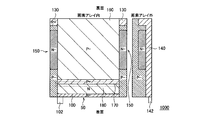
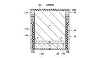
- FIG. 2 is a schematic diagram illustrating an imaging device (SPAD photodiode) 1000 according to an embodiment of the present disclosure.
- the configuration illustrated in FIG. 2 includes a multiplication region as a SPAD pixel, a photoelectric conversion unit 160 that performs photoelectric conversion, and includes a cathode electrode 100 and an anode electrode 130.
- the configuration shown in FIG. 2 is a back-illuminated type pixel.
- the substrate of the photodiode is thinned to 10 ⁇ m or less, and one anode electrode 130 of a pair of electrodes to which a high voltage is applied is located on the back side. Is provided.
- the front side of the semiconductor substrate 50 is the side on which the wiring layer is formed on the semiconductor substrate 50, and in the imaging device 100 of the present embodiment, the back side of the semiconductor substrate 50 is the light irradiation surface.
- the anode electrode 130 on the back side is provided corresponding to the pixel separating section 150.
- the thickness of the anode electrode 130 is, for example, 500 nm or more, and is a low-resistance electrode.
- the photoelectric conversion unit 160 is provided in a pixel region between the pixel separation units 150, and the outermost surface on the back side of the photoelectric conversion unit 160 is a light irradiation unit to which light is irradiated.
- the pixel region is defined by the distance of the pixel separating section 150, and has a rectangular planar shape of 5 ⁇ m or less in length and width.
- the anode electrode 130 is connected to a contact layer 140 formed by deep impurity implantation or metal embedding outside the pixel array, and the potential is taken out to the surface side.
- a predetermined voltage is applied to the electrode 142 connected to the contact layer 140 on the front surface side.
- a predetermined voltage is applied to the anode electrode 130 via the contact layer 140.
- the contact layer 140 be formed so as to surround the pixel array.
- the contact layer 140 may be provided at one place or may be divided into a plurality.
- the anode electrode 140 may have a plurality of contact layers 140 formed in the pixel array. As the number of contact layers 140 for taking out the electrode increases, the voltage fluctuation in the anode electrode 130 on the back surface side can be suppressed.
- the pixels are separated by the pixel separating unit 150 in the pixel array.
- FIG. 2 shows one pixel in the pixel array.
- the pixel separation section 150 is formed by changing the polarity of impurities with the photoelectric conversion section 160.
- the anode electrode 130 on the back side is provided corresponding to the position of the pixel separation unit 150, and is provided immediately above the pixel separation unit 150 in FIG.
- the pixel separation section 150 is formed by high-concentration impurity implantation, and the anode electrode 130 has a sufficient thickness, for example, 500 nm or more in order to sufficiently reduce the resistance. With such a structure, the depletion layer of the photoelectric conversion unit 160 can be formed up to the outermost surface on the back surface side of the pixel, and short wavelength sensitivity can be sufficiently maintained.
- an N-type impurity layer is formed on the front surface side to form the cathode electrode 100, and a P-type impurity layer is formed on the back surface side to form the anode electrode.
- An N-type layer (first semiconductor layer) 180 is connected to the cathode electrode 100.
- An electrode 102 is connected to the front side of the cathode electrode 100.
- the photoelectric conversion unit 160 connected to the anode electrode 130 is a low-concentration P-type, and has a high-concentration P-type layer (second semiconductor layer) 170 in contact with the photoelectric conversion unit (third semiconductor layer) 160 and an N-type cathode.
- a multiplication region in which a high electric field is generated is formed between the substrate and the mold layer 180. Further, a low-concentration N-type layer is used as the pixel separating section 150. Note that the P-type layer 170 may be expanded to the region of the photoelectric conversion unit 160 without providing the photoelectric conversion unit 160.
- the conductivity type and the concentration of the impurity layer are merely examples, and the anode and the cathode may be replaced with each other by replacing P and N.
- various other methods can be considered for forming the multiplication region in which a high electric field is generated.
- an impurity implantation region for isolating the multiplication region may be provided, or a buried insulating film or the like may be provided as the pixel separation unit 150.
- the anode electrode 130 and the cathode electrode 100 are provided on the front and back surfaces of the substrate.
- the anode electrode 130 on the back side is provided in the pixel separation region 150.
- the photoelectric conversion unit 160 formed of the depletion layer can be extended to the outermost surface of the light irradiation surface, so that the short-wavelength sensitivity can be significantly increased.
- the anode electrode 130 is located at the edge of the pixel, so that the electric field in the pixel is not constant and the depletion layer is difficult to spread to the surface of the photoelectric conversion unit 160 in the center of the pixel. Since the potential from the pixel end reaches the center of the pixel, a structure in which the anode electrode 130 on the back side is provided in the pixel separating section 150 can be adopted.
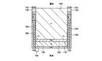
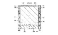
- FIG. 3 is a schematic diagram showing another configuration example of the present embodiment, in which a metal layer 152 having a light-shielding property is used as a pixel separating section 150 on the pixel surface on the back side.
- the metal layer 152 can be made of a metal such as tungsten (W).
- W tungsten
- a high-concentration impurity implantation region similar to that of FIG. The metal layer 152 may be in contact with the anode electrode 130 made of a high-concentration impurity region.
- the anode electrode 130 may be taken out to the front side similarly to FIG. 2, but may be directly connected to the bonding pad on the back side.
- the pixel separating unit 150 has a grid-like planar shape so as to surround a rectangular pixel area. For this reason, the anode electrode 130 formed on the pixel separation unit 150 and the metal layer 152 formed on the anode electrode 130 can also have a lattice planar shape following the pixel separation unit 150.
- a buried metal layer 190 having a light-shielding property is buried in the pixel separating section 150 from the front side.
- the buried metal layer 190 can be made of a metal such as tungsten (W), like the metal layer 152.
- the buried metal layer 190 and the photoelectric conversion unit 160 are separated by the insulating film 194, and the buried metal layer 190 is surrounded by the insulating film 194 between adjacent pixel regions.
- the buried metal layer 190 is buried from the front side to the middle of the photoelectric conversion section 160, and a high concentration impurity region is formed directly above the buried metal layer 190 to form the anode electrode 130 on the back side.
- the buried metal layer 190 having the configuration shown in FIG. 3 is buried from the back side.
- the anode electrode 130 composed of the high-concentration impurity region is formed in the pixel region so as to surround the buried metal layer 190.
- the provision of the buried metal layer 190 blocks the connection of the anode electrode 130 between pixels. Therefore, the metal layer 152 is provided on the pixel separating section 150, and the metal layer 152 and the anode electrode 130 are contacted to connect the anode electrode 130 between pixels.
- the metal 152 is insulated from the buried metal layer 190.
- the buried metal layer 190 may be buried only in a part of the photoelectric conversion unit 160, but is more preferably buried in the entire pixel region. With this structure, interference between pixels due to light is completely blocked, and interference between pixels due to voltage fluctuations is suppressed, so that miniaturization and high quantum efficiency can be achieved, and a low-noise pixel can be realized. .
- the anode electrode 130 is formed so as to correspond to the position of the pixel separation unit 150. It should be noted that the formation of the anode electrode 130 so as to correspond to the position of the pixel separation unit 150 means that the anode electrode 130 is formed immediately above the pixel separation unit 150 as shown in FIG. The case where the electrode 130 is formed on the pixel region side of the pixel separation unit 150 is included. Further, the anode electrode 130 is formed so as to correspond to the position of the pixel separating unit 150, but may not be provided to correspond to all of the pixel separating unit 150. May be provided correspondingly.
- FIG. 5 shows an example in which an auxiliary electrode 132 connected to the anode electrode 130 is provided on the outermost surface of the pixel region in the configuration example shown in FIG.
- the auxiliary electrode 132 has the same conductivity type as the anode electrode 130.
- the thickness of the auxiliary electrode 132 is, for example, 50 nm or less, so that the area of the photoelectric conversion unit 160 can be secured to the maximum.
- the auxiliary electrode 132 may be provided on the outermost surface on the back surface side in the pixel by implanting high-concentration impurities.
- the thickness of the region of the auxiliary electrode 132 in which impurities are implanted in the pixel is sufficiently thin, for example, 50 nm or less.
- the insulating layer 200 is provided over the auxiliary electrode 132, and light is emitted to the photoelectric conversion unit 160 through the insulating layer 200.
- the auxiliary electrode 132 By providing the auxiliary electrode 132, the potential of the outermost surface of the photoelectric conversion unit 160 on the back surface can be made constant, and the spread of the depletion layer and the electric field in the multiplication region can be uniformed in the pixel.
- the auxiliary electrode 132 has a small thickness and does not affect the short-wavelength sensitivity, it has a high resistance. However, since the resistance of the anode electrode 130 provided in the pixel separation portion is low, the potential of other pixels does not fluctuate.
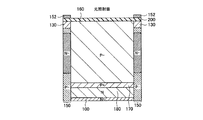
- the configuration example illustrated in FIG. 6 is different from the configuration example illustrated in FIG. 2 in that the insulating layer 200 is provided on the outermost surface (light irradiation surface) of the photoelectric conversion unit 160 and the insulating layer 200
- a metal layer 152 having a light shielding property is provided in FIG.
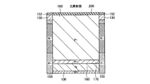
- the configuration example shown in FIG. 7 illustrates an example in which the metal layer 152 having a light-shielding property is provided on the anode electrode 130 without providing the insulating film 200 on the pixel separating unit 150.
- the metal layer 152 having a light-shielding property By providing the metal layer 152 having a light-shielding property, a light intrusion path can be divided for each pixel.
- the anode electrode 130 and the metal layer 152 having a light-shielding property can be set to the same potential.
- FIG. 8 shows an example in which the insulating layer 200 is provided on the light irradiation surface without providing the light-blocking metal layer 152 in the configuration example shown in FIG. 9 shows an example in which an insulating layer 200 and a metal layer 152 having a light-shielding property are provided in the configuration example shown in FIG. 3, similarly to the configuration example shown in FIG. 10 shows an example in which an insulating layer 200 and a metal layer 152 having a light-shielding property are provided in the configuration example shown in FIG. 3, similarly to the configuration example shown in FIG.
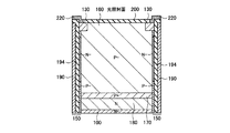
- the configuration example shown in FIG. 11 is different from the configuration example shown in FIG. 4 in that the anode electrode 130 is disposed closer to the pixel region than the pixel separation unit 150, and the surface metal provided on the anode electrode 130 and the pixel separation unit 150 is provided.
- An example in which layers 220 are connected is shown.
- the anode electrode 130 is connected to the anode electrode 130 in the adjacent pixel region by the surface metal layer 220.
- the surface metal layer 220 is formed so as to straddle the pixel separating section 150.
- the configuration example shown in FIG. 12 shows an example in which the length of the buried metal layer 190 is shortened in the depth direction of the pixel region (the photoelectric conversion unit 160) as compared with the configuration example shown in FIG.
- FIGS. 13 to 15 are schematic diagrams showing the positional relationship between the anode electrode 130 and the electrode 142 connected to the anode electrode 130.
- the electrode 142 is provided outside the pixel array and functions as a bonding pad (lead electrode).
- FIG. 13 illustrates an example in which the contact layer 140 is provided as in FIG. 2, whereby the anode electrode 130 is drawn out to the front side through the contact layer 140 and the contact layer 140 and the front-side electrode 142 are connected. Note that the contact layer 140 may be connected to circuits around the pixel array.
- FIG. 14 shows an example in which an electrode 142 is provided on the same back side as the anode electrode 130 and the anode electrode 130 and the electrode 142 are directly connected.
- an electrode 142 as a bonding pad is provided on the back surface side.
- a metal layer 152 having a light-shielding property may be provided on the anode electrode 130, and the metal layer 152 may be connected to the electrode 142 as a bonding pad.
- FIG. 15 is an example in which an electrode 142 is provided on the front surface side in the same manner as the example shown in FIG. 13. However, an electrode 152 connected to the anode electrode 130 is provided, and the electrode 152 It is a schematic diagram which shows the example which performed connection.
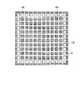
- FIGS. 16 and 17 are plan views showing the positional relationship between the anode electrode 130 and the contact layer 140, as viewed from the light irradiation surface side (back surface side).
- the inside of the dashed line R is a region inside the pixel array
- the outside of the dashed line R is a region outside the pixel array.
- the anode electrode 130 has a lattice shape.
- the metal layer 152 having a light-shielding property is provided, the metal layer 152 having a shape following the grid-like anode electrode 130 shown in FIG.
- the metal layer 152 having the light-shielding property can be formed on the anode electrode 130 via the insulating layer 200 as shown in FIG. 6, the metal layer 152 and the anode electrode 130 are not integrated.
- the position of the metal layer 152 can be shifted from the pixel separating section 150 (the anode electrode 130) toward the periphery.
- a contact layer 140 is provided so as to surround the pixel array. As shown in FIG. 2, the anode electrode 130 is drawn out to the front side via the contact layer 140.
- FIG. 17 shows an example in which a contact layer 140 is provided in the pixel array in addition to the configuration of FIG.
- a contact layer 140 is provided in the pixel array in addition to the configuration of FIG.
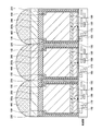
- FIG. 18 shows a configuration shown in FIG. 12, in which color filters 300a, 300b, and 300c are provided on the insulating layer 200 on the light irradiation surface, and further above the color filters 300a, 300b, and 300c.
- FIG. 2 is a schematic cross-sectional view illustrating a configuration in which an on-chip lens 400 is provided. Light transmitted through the on-chip lens 400 and the color filters 300a, 300b, 300c is applied to the photoelectric conversion unit 160. Note that in FIG. 18, the insulating film 194 of the pixel separation section 150 shown in FIG. 12 is provided in common with the insulating layer 200 on the light irradiation surface.
- FIG. 19 is a schematic diagram showing a state in which a region on the photoelectric conversion unit 160 side is viewed from the interface between the photoelectric conversion unit 160 and the insulating layer 200 shown in FIG.
- a pixel separation unit 150 is provided from a buried metal layer 190 and an insulation layer 200 (insulation film 194), and a pixel region including the photoelectric conversion unit 160 is defined by the pixel separation unit 150.
- the anode electrode 130 is provided so as to surround the pixel region along the pixel separation unit 150.
- FIG. 20 is a block diagram illustrating a configuration example of a camera device 2000 as an electronic device to which the present technology is applied.
- a camera device 2000 illustrated in FIG. 20 includes an optical unit 2100 including a lens group, the above-described imaging device (imaging device) 1000, and a DSP circuit 2200 that is a camera signal processing device.
- the camera device 2000 also includes a frame memory 2300, a display unit (display device) 2400, a recording unit 2500, an operation unit 2600, and a power supply unit 2700.
- the DSP circuit 2200, the frame memory 2300, the display unit 2400, the recording unit 2500, the operation unit 2600, and the power supply unit 2700 are mutually connected via a bus line 2800.
- the optical unit 2100 captures incident light (image light) from a subject and forms an image on the imaging surface of the imaging device 1000.
- the imaging device 1000 converts the amount of incident light formed on the imaging surface by the optical unit 2100 into an electric signal for each pixel and outputs the electric signal as a pixel signal.
- the display unit 2400 includes a panel-type display device such as a liquid crystal panel or an organic EL (Electro Luminescence) panel, and displays a moving image or a still image captured by the imaging device 1000.
- the DSP circuit 2200 receives a pixel signal output from the imaging device 1000 and performs a process for displaying the pixel signal on the display unit 2400.
- the recording unit 2500 records a moving image or a still image captured by the imaging device 1000 on a recording medium such as a video tape or a DVD (Digital Versatile Disk).
- the operation unit 2600 issues an operation command for various functions of the imaging apparatus 1000 under the operation of the user.
- the power supply unit 2700 appropriately supplies various power supplies serving as operation power supplies for the DSP circuit 2200, the frame memory 2300, the display unit 2400, the recording unit 2500, and the operation unit 2600 to these supply targets.
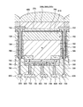
- FIG. 21A is a schematic cross-sectional view showing a basic configuration common to each variation.
- the imaging device 1000 illustrated in FIG. 21A includes a multiplication region as a SPAD pixel and a photoelectric conversion unit (N-region) 160 that performs photoelectric conversion, and the outermost surface on the back side of the photoelectric conversion unit 160 is irradiated with light. It is an irradiation unit.
- the metal layer 152 functioning as the anode electrode 130 is electrically connected to the P region 760.
- the P region 760 is configured such that the lower the layer, the lower the impurity concentration.
- a P region 700 and a P ⁇ region 710 are formed from the P region 760 along the pixel separating section 150, and the P region 760 and the avalanche section 720 are electrically connected.
- the avalanche portion 720 is configured by joining a P + region 730 and an N + region 740.
- the P region 700 is configured by accumulating reverse charges (holes) so that charges (electrons) to be read out by the avalanche section 720 pass through.
- the P ⁇ region 710 is desirably a low concentration region in order to increase the central potential so that electric charges pass through the avalanche portion 720.
- the N + region 740 is connected to the electrode 102 via the N + region 750.
- An N ⁇ region 780 is formed on the side surface of the P + region 730 and the N + region 740.
- a P + layer 790 that is electrically connected to the N + region 740 and the N ⁇ region 780 is provided, and the P + layer 790 is grounded (GND) via the electrode 800.
- the P + layer 790 may be an N layer.
- an electrode such as the wiring layer 820 connected to the P + layer 790 may not be formed.
- the electrode 102 is an electrode that outputs a signal corresponding to the incident light.
- the electrode 800 is an electrode for discharging holes. Note that the P + layer 790 and the electrode 800 need not be provided.
- the buried metal layer 190 provided in the electrode 102, the electrode 800, and the pixel separation unit 150 is connected to the wiring layer 820, respectively.
- the wiring layer 820 shows a part of the uppermost wiring layer among the wiring layers shown in FIG.
- the P + layer 790 may be an N layer. Further, an electrode such as the wiring layer 820 connected to the P + layer 790 may not be provided.
- An insulating film (fixed charge film) 810 is provided on the side surface of the pixel separating section 150 and on the upper layer of the P region 760.
- the insulating film 810 is, for example, negatively charged.
- the configuration of the upper layer of P region 760 is basically the same as the configuration shown in FIG. Note that in the configuration shown in FIG. 21A, the imaging device 1000 can be configured by exchanging the P-type and N-type conductivity types.
- the N + region 740 and the N + region 750 correspond to the N-type layer 180 shown in FIG.
- the P region 760, the P region 700, and the P ⁇ region 710 correspond to the photoelectric conversion unit (third semiconductor layer) 160 and the P-type layer 170.
- FIG. 21A is a schematic cross-sectional view showing an example in which the metal layer 152 in FIG. 21A is covered with the same insulating film 200 as in FIG. 18 and color filters 300a, 300b, and 300c are provided.
- the first variation relates to a configuration in which the anode electrode 130 is a metal layer 152 and the buried metal layer 190 is electrically connected to the anode electrode 130 (metal layer 152).
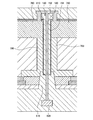
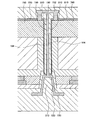
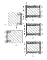
- FIG. 22A is a schematic cross-sectional view showing the vicinity of the pixel separation unit 150 in detail regarding the imaging device 1000 of the first variation.
- a buried metal layer 190 is provided so as to penetrate the pixel separating section 150.
- the buried metal layer 190 is electrically connected to the P region 760 on the back surface via the metal layer 152.
- the parasitic resistance of the anode electrode can be reduced, and the voltage drop particularly at the center of the pixel area can be reduced. Become.
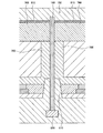
- FIGS. 22B to 22H are schematic cross-sectional views showing different modes of the imaging device 1000 according to the first variation. 22B to 22H, the buried metal layer 190 and the metal layer 152 are electrically connected.
- FIG. 22B illustrates an example in which the pixel separation unit 150 is covered with the metal layer 152.
- FIG. 22C shows an example in which the width of the pixel separating section 150 from the back surface to the front surface is made constant without forming the buried insulating film 510 on the front surface as shown in FIG. 22A.
- FIG. 22D shows an example in which a buried insulating film 510 shown in FIG. 22A is dug to form a recess 520, and a buried metal layer 530 connected to the buried metal layer 190 is formed in the recess 520.
- FIG. 22E is a schematic diagram showing an example in which the buried metal layer 190 is formed without providing the insulating film 194 in the configuration shown in FIG. 22A.
- FIG. 22E shows a configuration in which the upper end surface of the buried metal layer 190 protrudes above the upper surface of the insulating film 810, but the upper end surface of the buried metal layer 190 is at the same position as the upper surface of the insulating film 810. Is also good.
- FIG. 22F shows a configuration in which the embedded metal layer 190 is not connected to the wiring layer 820 in the configuration shown in FIG. 22A.
- FIG. 22G illustrates a structure in which the insulating film 810 is extended to a lower portion of the buried insulating film 510 in the structure illustrated in FIG. 22A.
- FIG. 22H shows a structure in which a high-concentration P layer 830 is provided on the side of the buried metal layer 190 without providing the insulating film 810 in the structure shown in FIG. 22A.
- the high-concentration P layer 830 corresponds to a P layer 544 shown in a manufacturing process of FIG. 25 described later.
- a high-concentration P layer 830 may be formed instead of the insulating film 810. Note that in FIG. 22H, the insulating film 810 formed over the P region 760 may not be provided. 22A to 22C, 22E, 22G, and 22H, the buried metal layer 190 is connected to the wiring layer 820 on the opposite side of the metal layer 152.
- the buried metal layer 190 and the wiring layer 820 By connecting the buried metal layer 190 and the wiring layer 820, the area as the anode wiring is increased, and the resistance of the anode can be further reduced. Further, by connecting the buried metal layer 190 and the wiring layer 820, leakage of light and color mixing in adjacent pixels can be further suppressed. Further, since the buried metal layer 190 is connected to the wiring layer 820 extending in the horizontal direction or the wiring layer 820 formed deeper than the substrate, light is reflected by the lower wiring layer 820 and light enters adjacent pixels. Can be suppressed. In addition, the obliquely incident light can be reflected by the horizontal wiring layer 820 connected to the buried metal layer 190, and the light can be re-incident on a pixel to be detected.
- charges holes collected by the P-type
- the light incident surface side upper side
- the lower wiring layer 820 can be arbitrarily formed similarly to the upper wiring layout.
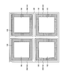
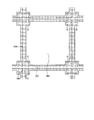
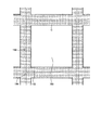
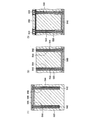
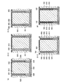
- FIGS. 23A to 23G are plan views of the imaging device 1000 according to the first variation.
- the example illustrated in FIG. 23A corresponds to the configuration in FIG. 22A, and the metal layer 152 is formed along the pixel separation unit 150 with a wider width than the buried metal layer 190.
- 23A to 23G the region of the metal layer 152 is indicated by dots, and a portion C where the metal layer 152 is electrically connected to the P region 760 is shown.
- the example shown in FIG. 23A shows a configuration in which the portion C where the metal layer 152 is electrically connected to the P region 760 is four places per pixel.
- the example illustrated in FIG. 23B illustrates a configuration in which, in the configuration of FIG.
- a portion C where the metal layer 152 is electrically connected to the P region 760 is one per pixel.
- portions C where the metal layer 152 is electrically connected to the P region 760 are provided along four sides along the buried metal layer 190, and the metal layer 152 is formed in the P region 760.
- FIG. 3 shows a configuration in which a portion C electrically connected to a ring is formed.
- the portion C where the metal layer 152 is electrically connected to the P region 760 may be only one side along the buried metal layer 190.
- the example shown in FIG. 23D corresponds to the configuration in FIG. 22B. In the example shown in FIG. 23D, similarly to FIG.
- the metal layer 152 is formed along the pixel separation portion 150 with a wider width than the buried metal layer 190, and the P region adjacent to the buried metal layer 190 at the four corners of the pixel.
- a portion C electrically connected to 760 is provided.
- FIG. 23E illustrates a configuration in which only one portion C electrically connected to the P region 760 is provided in one pixel in FIG. 23D.
- FIG. 23F illustrates a configuration in which the planar shape of the portion C electrically connected to the P region 760 in FIG. 23D is triangular. According to the configuration of FIG. 23F, the opening of the metal layer 152 on which light enters can be further expanded.
- the planar shape of the portion C electrically connected to the P region 760 may be a shape other than a triangle, and may be, for example, a circle.
- the example illustrated in FIG. 23G is a schematic diagram illustrating an example in which a portion C electrically connected to the P region 760 is provided along the buried metal layer 190 in FIG. 23D.
- the portion C where the metal layer 152 is electrically connected to the P region 760 may be only one side along the buried metal layer 190.
- the metal layer 152 does not protrude toward the photoelectric conversion unit side from the pixel separation unit 150 except for the part C electrically connected to the P region 760.
- FIG. 24 is a schematic cross-sectional view showing a method of manufacturing the semiconductor device according to the first variation in the order of steps.
- step (1) necessary N layers and P layers are formed in the Si substrate 520 by ion implantation and heat treatment, and a desired structure is formed by film formation or the like, and a buried insulating film is formed so as to surround the pixels.
- the first layer 528 in which the insulating film is embedded is formed. Thereby, each N region and each P region shown in FIG. 21A are formed. In FIG. 24, illustration of each N region and each P region is omitted.
- a metal layer 530 is formed over the first layer 528 in which the insulating film is embedded, and a structure in which the metal layer 530 is embedded in the first layer 528 is obtained by forming an insulating film.
- the burying of the first layer 528 such as an oxide film, a nitride film, and a stack of an oxide film and a nitride film can be considered. It is desirable that the metal layer 530 be formed of tungsten (W) or the like. Note that the metal layer 530 need not be formed.
- step (2) after forming a necessary wiring layer, the front and back surfaces are inverted by a method such as bonding, and unnecessary layers are removed.
- step (3) after etching the Si substrate 520 so as to reach the buried insulating film, an insulating film 532 made of aluminum oxide (Al 2 O 3 ), hafnium oxide (HfO 2 ) or the like, and an oxide film An insulating film 534 made of, for example, is formed. For the film formation, it is preferable to use a film type having good coverage.
- a trench (trench) penetrating the first burying layer 528 and reaching the metal layer 530 is formed, and the metal film 536 is buried.
- the metal film 536 be formed of tungsten (W) or the like. After penetrating the Si layer 526 and the first burying layer 528, an insulating film 532 and an insulating film 534 may be formed and the metal layer 536 may be buried. Finally, in the step (5), after the insulating film 200 is formed, an electrode 538 for making a back contact is formed. Through these steps, an element having a back electrode is manufactured. Note that the N layer and the P layer may be reversed. In that case, the type of the insulating film 532 is changed. Then, color filters 300a, 300b, 300c and an on-chip lens 400 (not shown in FIG. 24) as shown in FIG. 21A are formed on the insulating film 200 and the electrodes 538.
- W tungsten
- FIG. 25 is a schematic diagram showing a manufacturing process in this case.
- step (1) necessary N layers and P layers are formed in the Si substrate 520 by ion implantation and heat treatment, and a desired structure is formed by film formation or the like. Thereby, each N region and each P region shown in FIG. 21A are formed.
- the second layer 540 is embedded in the Si substrate 520, and the metal film 542 is embedded in the second layer 540.
- a high-concentration P layer 544 is formed on the Si substrate 520 adjacent to the second layer 540 by using solid-phase diffusion or the like.
- step (2) the front and back surfaces are inverted, and unnecessary layers are removed. Then, after a predetermined insulating film is formed on the Si substrate 520, an electrode 538 for making a back contact is formed in the same manner as in the step (5) in FIG. Then, color filters 300a, 300b, 300c and an on-chip lens 400 (not shown in FIG. 24) as shown in FIG. 21A are formed on the insulating film 200 and the electrodes 538.
- the insulating film 532 corresponds to the insulating film 810 in FIGS. 22A to 22F
- the metal layer 536 corresponds to the buried metal layer 190 in FIGS. It corresponds to the layer 152 (anode electrode).
- the buried metal layer 190 and the metal layer 152 may be formed of the same material, and for example, may be formed of a metal such as tungsten (W).
- the metal layer 152 functioning as the anode electrode 130 is electrically connected to the P region 760 of the photoelectric conversion unit 160, the parasitic resistance of the anode wiring can be reduced. Become. Since the metal layer 152 functioning as the anode electrode 130 is electrically connected to the P region 760 of the photoelectric conversion unit 160, a voltage drop at the center of the pixel region can be suppressed.
- the metal layer 152 (anode electrode) connected to the P region 760 is formed along the pixel separation section 150 as shown in FIG. Therefore, a sufficient contact area between P region 760 and metal layer 152 can be ensured, and the contact resistance between P region 760 and metal layer 152 can be reduced.
- the photoelectric conversion unit of each pixel is reduced by the wiring layer 500 formed inside the pixel separation unit 150.
- the buried metal layer 190 and the metal layer 152 are electrically connected.
- the P area 760 is dug to increase the contact area and reduce the contact resistance.
- the area occupied by the wiring layer 500 inside the pixel separation unit 150 is reduced by the amount of the increase in the contact area, and the area of the photoelectric conversion unit of each pixel is secured to the maximum.
- the sensitivity of the imaging device 1000 can be further improved without increasing the image quality.
- FIG. 26 is a schematic cross-sectional view showing an imaging device 1000 according to the second variation.
- a contact portion 152a of metal layer 152 connected to P region 760 is filled in a region dug in P region 760.
- the region dug in the P region 760 may have a plurality of shapes such as a groove shape, a hole shape, and a shape connected to a groove formed by engraving between pixels.
- the metal layer 152 does not protrude to the photoelectric conversion unit side from the pixel separation unit 150 except for the region where the contact unit 152a is formed.
- the contact area between contact portion 152a and P region 760 increases, and the contact resistance can be reduced.
- FIG. 27 is a schematic sectional view showing an imaging device 1000 according to the third variation.
- an insulating film 810 is formed along the insulating film 194 of the pixel separation section 150.
- the position of the upper end of the insulating film 810 along the pixel separating section 150 has receded to a position lower than the upper end of the insulating film 194 of the pixel separating section 150.
- the distance d1 shown in FIG. 27 indicates the amount of retreat in the downward direction of the insulating film 700.
- FIG. 28 is an enlarged schematic diagram showing the range of the region A1 shown in FIG. 27, and shows states before and after the metal layer 152 is filled, respectively.
- FIG. 28 shows the vicinity of the insulating film 810 in more detail.
- a film 193 formed of tantalum oxide (Ta 2 O 5 ) or the like and an insulating film 192 are formed adjacent to the insulating film 810. Since the film 193 is formed by the sputtering method, the coverage is relatively low, and is not formed on the side wall of the groove 701.
- the insulating film 192 is formed by CVD or the like and has good coverage. The state before filling of the metal layer 152 shown on the left side of FIG.
- FIG. 28 shows a state where a groove 701 for filling the buried metal layer 190 is formed in the pixel separating section 150 and an opening 702 is formed on the pixel separating section 150. I have. In this state, the trench 701 is not filled with the buried metal layer 190, and the opening 702 is not filled with the metal layer 152.
- a dashed line in FIG. 28 indicates a range of the opening 702 before the insulating film 810 is retracted. After forming the opening 702 in the range shown by the broken line, the insulating film 810 is receded by a cleaning step.
- the insulating film 700 recedes vertically by a distance d1 and recedes horizontally by a distance d2.
- the retreat amount is about several nm to several tens nm.
- the buried metal layer 190 is formed so as to fill the groove 701, and the metal layer 152 is formed so as to fill the opening 702. Accordingly, the region of the metal layer 152 connected to the P region 760 expands by the amount of the recess of the insulating film 810, and the contact resistance between the P region 760 and the metal layer 152 can be reduced.
- the metal layer 152 and the buried metal film 190 are formed integrally.
- the contact region between the P region 760 and the metal layer 152 can be enlarged by retreating the insulating film 810. Therefore, according to the configuration of the third variation shown in FIG. 27, it is possible to further reduce the contact resistance between P region 760 and metal layer 152.
- FIG. 29 is a schematic sectional view showing another example of the third variation.
- the contact of the metal layer 152 with the P region 760 is performed at a position separated from the pixel separating section 150.
- FIG. 30 is a schematic diagram showing an enlarged range of the area A2 shown in FIG. A broken line shown in FIG. 30 indicates a range of the opening 704 before the insulating film 810 is retracted. After the opening 704 is formed in the range shown by the broken line, the insulating film 810 is receded in the horizontal direction by a distance d2 by a cleaning process.
- a metal layer 152 is formed so as to fill the opening 704.
- the region where metal layer 152 and P region 760 are in contact with each other is expanded by the amount that insulating film 810 is receded in the horizontal direction, and the contact resistance between metal layer 152 and P region 760 is reduced. Can be.
- FIG. 31 is a schematic cross-sectional view showing a method for manufacturing a semiconductor device according to the third variation in the order of steps.
- step (4) in FIG. 31 the Si layer 926 is etched to reach the buried insulating film, and then aluminum oxide (Al)
- Al aluminum oxide
- An insulating film 810 made of 2 O 3 ), hafnium oxide (HfO 2 ), or the like, and an insulating film 934 made of an oxide film or the like are formed.
- the insulating film 810 recedes downward and horizontally.
- the insulating film 810 is formed using aluminum oxide (Al 2 O 3 ), hafnium oxide (HfO 2 ), or the like, the insulating film 810 is formed using an inorganic chemical solution of DHF or a general organic chemical solution used for cleaning after processing. It is retracted by about several nm to several tens nm.
- the metal film 936 is embedded. It is desirable that the metal film 936 be formed of tungsten (W) or the like. Sputtering, CVD, or the like can be used as a method for forming a metal film, but CVD (Chemical Vapor Deposition) is more advantageous for coverage.
- the metal layer 936 is filled in a region including the inside of the groove and the opening 702 formed in the step (5).
- the metal layer 936 is also filled in a portion where the insulating film 810 is recessed.
- the filled metal layer 936 corresponds to the buried metal layer 190 and the metal layer 152.
- the P layer 924 corresponds to the P region 760 in FIG. After that, the color filters 300a, 300b, 300c and the on-chip lens 400 (not shown in FIG. 31) as shown in FIG. 21A are formed.
- the insulating film 810 recedes downward and horizontally in the cleaning step of step (5). Then, by filling the metal layer 936 in the step (6), the metal layer 936 is filled in the portion where the insulating film 810 is recessed, so that the contact area between the metal layer 936 and the P region 760 is increased, Resistance is reduced.
- the opening 704 may be formed at a position separated from the pixel separating section 150 in the step (5).
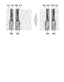
- FIG. 32 shows an example in which the insulating film 810 formed on the first buried layer 928 in the trench recedes in the step (5) of FIG. 31 and an insulating film is further formed on this portion. It is an outline sectional view.
- FIG. 33 is an enlarged cross-sectional view showing the region A3 in the step (5-1) and the step (5-2) shown in FIG.
- a cleaning process is performed, so that the insulating film 810 is exposed on the first buried layer 928.
- the insulating film 810 is recessed on the first buried layer 928. Since the withstand voltage of the pixel separation unit 150 may decrease due to the receding, in FIG. 32, an insulating film 950 is formed in the contact hole in the step (5-2), and the contact film is formed on the first buried layer 928.
- the insulating film 810 exposed in the hole is covered with the insulating film 950.
- ALD Atomic Layer Deposition
- the insulating film 810 is covered with the insulating film 950 on the first burying layer 928 as shown in the right side diagram of FIG.
- the insulating film 950 in a portion where the insulating film 810 has receded remains, and the insulating film in an unnecessary portion can be removed.
- a step (5-3) an opening 702 is formed and a cleaning step is performed, so that the insulating film 810 is receded downward and horizontally, as in the step (5) shown in FIG. Subsequent steps are the same as in FIG.
- the contact area between the metal layer 152 and the P region 760 can be increased by retreating the insulating film 810, and the contact resistance can be reduced.
- the withstand voltage can be improved by retreating the insulating film 810 on the side wall of the pixel separating portion 150 which is not the contact portion and embedding the insulating film.
- Example of application to devices other than imaging device The present disclosure can also be applied to other devices that detect light, such as a TOF (Time Of Flight) sensor.
- a TOF sensor When applied to a TOF sensor, for example, it can be applied to a range image sensor based on a direct TOF measurement method and a range image sensor based on an indirect TOF measurement method.
- an optical pulse having a short pulse width is transmitted and an electric pulse is generated by a receiver that responds at a high speed in order to directly determine the arrival timing of a photon in each pixel in a time domain.
- the present disclosure can be applied to a receiver at that time.
- the time of flight of light is measured using a semiconductor element structure in which the amount of carriers generated and generated by light changes depending on the arrival timing of light.
- the present disclosure can be applied to such a semiconductor structure.
- it is optional to provide the color filters 300a, 300b, 300c and the on-chip lens 400 as shown in FIG. 18, and these may not be provided.
- FIG. 34 is a schematic diagram illustrating a configuration of an electronic device 3000 including the above-described imaging device 1000.
- An electronic device 3000 illustrated in FIG. 34 includes a first semiconductor chip 3100 having a sensor unit 3010 in which a plurality of photoelectric conversion units 160 are arranged, and a signal processing unit 3020 that processes a signal acquired by the photoelectric conversion unit 160. And a second semiconductor chip 3200. The first semiconductor chip 3100 and the second semiconductor chip 3200 are stacked.
- a control unit 3030 that controls the electronic device 3000 and a memory unit 3040 that stores signals acquired by the photoelectric conversion unit 160 are provided near the signal processing unit 3020.
- the control unit 3030 can be arranged, for example, in the vicinity of the photoelectric conversion unit 160 for the purpose of another drive or control in addition to the control of the signal processing unit 3020.
- the control unit 3030 can be provided in any region of the first semiconductor chip 3100 and the second semiconductor chip 3200 so as to have any function other than the arrangement shown in the drawing.
- the plurality of photoelectric conversion units 160 are arranged in a two-dimensional matrix (matrix).
- FIG. 34 shows the first semiconductor chip 3100 and the second semiconductor chip 3200 in a separated state for the sake of explanation.
- the technology (the present technology) according to the present disclosure can be applied to various products.
- the technology according to the present disclosure is realized as a device mounted on any type of moving object such as an automobile, an electric vehicle, a hybrid electric vehicle, a motorcycle, a bicycle, a personal mobility, an airplane, a drone, a ship, and a robot. You may.
- FIG. 35 is a block diagram illustrating a schematic configuration example of a vehicle control system that is an example of a moving object control system to which the technology according to the present disclosure can be applied.
- Vehicle control system 12000 includes a plurality of electronic control units connected via communication network 12001.
- the vehicle control system 12000 includes a drive system control unit 12010, a body system control unit 12020, an outside information detection unit 12030, an inside information detection unit 12040, and an integrated control unit 12050.
- a microcomputer 12051, an audio / video output unit 12052, and a vehicle-mounted network I / F (Interface) 12053 are illustrated.
- the drive system control unit 12010 controls the operation of the device related to the drive system of the vehicle according to various programs.
- the driving system control unit 12010 includes a driving force generating device for generating driving force of the vehicle such as an internal combustion engine or a driving motor, a driving force transmission mechanism for transmitting driving force to wheels, and a steering angle of the vehicle. It functions as a control mechanism such as a steering mechanism for adjusting and a braking device for generating a braking force of the vehicle.
- the body control unit 12020 controls the operation of various devices mounted on the vehicle body according to various programs.
- the body control unit 12020 functions as a keyless entry system, a smart key system, a power window device, or a control device for various lamps such as a head lamp, a back lamp, a brake lamp, a blinker, and a fog lamp.
- a radio wave or various switch signals transmitted from a portable device replacing the key may be input to the body control unit 12020.
- the body control unit 12020 receives the input of these radio waves or signals and controls a door lock device, a power window device, a lamp, and the like of the vehicle.
- Out-of-vehicle information detection unit 12030 detects information external to the vehicle on which vehicle control system 12000 is mounted.
- an imaging unit 12031 is connected to the outside-of-vehicle information detection unit 12030.
- the out-of-vehicle information detection unit 12030 causes the imaging unit 12031 to capture an image outside the vehicle, and receives the captured image.
- the out-of-vehicle information detection unit 12030 may perform an object detection process or a distance detection process of a person, a vehicle, an obstacle, a sign, a character on a road surface, or the like based on the received image.
- the imaging unit 12031 is an optical sensor that receives light and outputs an electric signal according to the amount of received light.
- the imaging unit 12031 can output an electric signal as an image or can output the information as distance measurement information.
- the light received by the imaging unit 12031 may be visible light or non-visible light such as infrared light.
- the in-vehicle information detection unit 12040 detects information in the vehicle.
- the in-vehicle information detection unit 12040 is connected to, for example, a driver status detection unit 12041 that detects the status of the driver.
- the driver state detection unit 12041 includes, for example, a camera that captures an image of the driver, and the in-vehicle information detection unit 12040 determines the degree of driver fatigue or concentration based on the detection information input from the driver state detection unit 12041. The calculation may be performed, or it may be determined whether the driver has fallen asleep.
- the microcomputer 12051 calculates a control target value of the driving force generation device, the steering mechanism or the braking device based on the information on the inside and outside of the vehicle acquired by the outside information detection unit 12030 or the inside information detection unit 12040, and the drive system control unit A control command can be output to 12010.
- the microcomputer 12051 realizes functions of an ADAS (Advanced Driver Assistance System) including a vehicle collision avoidance or a shock mitigation, a following operation based on an inter-vehicle distance, a vehicle speed maintaining operation, a vehicle collision warning, or a vehicle lane departure warning. Cooperative control for the purpose.
- ADAS Advanced Driver Assistance System
- the microcomputer 12051 controls the driving force generation device, the steering mechanism, the braking device, and the like based on the information about the surroundings of the vehicle obtained by the outside information detection unit 12030 or the inside information detection unit 12040, so that the driver 120 It is possible to perform cooperative control for automatic driving or the like in which the vehicle travels autonomously without depending on the operation.
- the microcomputer 12051 can output a control command to the body system control unit 12030 based on the information on the outside of the vehicle obtained by the outside information detection unit 12030.
- the microcomputer 12051 controls the headlamp in accordance with the position of the preceding vehicle or the oncoming vehicle detected by the outside-of-vehicle information detection unit 12030, and performs cooperative control for the purpose of preventing glare such as switching a high beam to a low beam. It can be carried out.
- the sound image output unit 12052 transmits at least one of a sound signal and an image signal to an output device capable of visually or audibly notifying a passenger of the vehicle or the outside of the vehicle of information.
- an audio speaker 12061, a display unit 12062, and an instrument panel 12063 are illustrated as output devices.
- the display unit 12062 may include, for example, at least one of an on-board display and a head-up display.
- FIG. 36 is a diagram illustrating an example of an installation position of the imaging unit 12031.
- imaging unit 12031 there are imaging units 12101, 12102, 12103, 12104, and 12105.
- the imaging units 12101, 12102, 12103, 12104, and 12105 are provided, for example, at positions such as a front nose, a side mirror, a rear bumper, a back door, and an upper part of a windshield in the vehicle interior of the vehicle 12100.
- the imaging unit 12101 provided on the front nose and the imaging unit 12105 provided above the windshield in the passenger compartment mainly acquire an image in front of the vehicle 12100.
- the imaging units 12102 and 12103 provided in the side mirror mainly acquire images of the side of the vehicle 12100.
- the imaging unit 12104 provided in the rear bumper or the back door mainly acquires an image behind the vehicle 12100.
- the imaging unit 12105 provided above the windshield in the passenger compartment is mainly used for detecting a preceding vehicle or a pedestrian, an obstacle, a traffic light, a traffic sign, a lane, or the like.
- FIG. 36 shows an example of the imaging range of the imaging units 12101 to 12104.
- the imaging range 12111 indicates the imaging range of the imaging unit 12101 provided on the front nose
- the imaging ranges 12112 and 12113 indicate the imaging ranges of the imaging units 12102 and 12103 provided on the side mirrors, respectively
- the imaging range 12114 indicates 13 shows an imaging range of an imaging unit 12104 provided in a rear bumper or a back door.
- a bird's-eye view image of the vehicle 12100 viewed from above is obtained by superimposing image data captured by the imaging units 12101 to 12104.
- At least one of the imaging units 12101 to 12104 may have a function of acquiring distance information.
- at least one of the imaging units 12101 to 12104 may be a stereo camera including a plurality of imaging elements or an imaging element having pixels for detecting a phase difference.
- the microcomputer 12051 calculates a distance to each three-dimensional object in the imaging ranges 12111 to 12114 and a temporal change of the distance (relative speed with respect to the vehicle 12100).
- a distance to each three-dimensional object in the imaging ranges 12111 to 12114 and a temporal change of the distance (relative speed with respect to the vehicle 12100).
- microcomputer 12051 can set an inter-vehicle distance to be secured before the preceding vehicle and perform automatic brake control (including follow-up stop control), automatic acceleration control (including follow-up start control), and the like. In this way, it is possible to perform cooperative control for automatic driving or the like in which the vehicle travels autonomously without depending on the operation of the driver.
- the microcomputer 12051 converts the three-dimensional object data relating to the three-dimensional object into other three-dimensional objects such as a motorcycle, a normal vehicle, a large vehicle, a pedestrian, a telephone pole, and the like based on the distance information obtained from the imaging units 12101 to 12104. It can be classified and extracted and used for automatic avoidance of obstacles. For example, the microcomputer 12051 distinguishes obstacles around the vehicle 12100 into obstacles that are visible to the driver of the vehicle 12100 and obstacles that are difficult to see. Then, the microcomputer 12051 determines a collision risk indicating a risk of collision with each obstacle, and when the collision risk is equal to or more than the set value and there is a possibility of collision, via the audio speaker 12061 or the display unit 12062. By outputting an alarm to the driver through forced driving and avoidance steering via the drive system control unit 12010, driving assistance for collision avoidance can be performed.
- driving assistance for collision avoidance can be performed.
- At least one of the imaging units 12101 to 12104 may be an infrared camera that detects infrared light.
- the microcomputer 12051 can recognize a pedestrian by determining whether or not a pedestrian exists in the captured images of the imaging units 12101 to 12104. The recognition of such a pedestrian is performed by, for example, extracting a feature point in an image captured by the imaging units 12101 to 12104 as an infrared camera, and performing a pattern matching process on a series of feature points indicating the outline of the object to determine whether the object is a pedestrian.
- the audio image output unit 12052 outputs a rectangular contour for emphasis to the recognized pedestrian.
- the display unit 12062 is controlled so that is superimposed. Further, the sound image output unit 12052 may control the display unit 12062 so as to display an icon or the like indicating a pedestrian at a desired position.
- Example of Application to Endoscopic Surgery System The technology (the present technology) according to the present disclosure can be applied to various products.
- the technology according to the present disclosure may be applied to an endoscopic surgery system.
- FIG. 37 is a diagram illustrating an example of a schematic configuration of an endoscopic surgery system to which the technology (the present technology) according to the present disclosure may be applied.
- FIG. 37 shows a state in which an operator (doctor) 11131 is performing an operation on a patient 11132 on a patient bed 11133 using the endoscopic surgery system 11000.
- the endoscopic surgery system 11000 includes an endoscope 11100, other surgical tools 11110 such as an insufflation tube 11111 and an energy treatment tool 11112, and a support arm device 11120 that supports the endoscope 11100.
- a cart 11200 on which various devices for endoscopic surgery are mounted.
- the endoscope 11100 includes a lens barrel 11101 having a predetermined length from the distal end inserted into the body cavity of the patient 11132, and a camera head 11102 connected to the proximal end of the lens barrel 11101.
- the endoscope 11100 which is configured as a so-called rigid endoscope having a hard lens barrel 11101 is illustrated.
- the endoscope 11100 may be configured as a so-called flexible endoscope having a soft lens barrel. Good.
- An opening in which an objective lens is fitted is provided at the tip of the lens barrel 11101.
- a light source device 11203 is connected to the endoscope 11100, and light generated by the light source device 11203 is guided to the distal end of the lens barrel by a light guide that extends inside the lens barrel 11101, and the objective The light is radiated toward the observation target in the body cavity of the patient 11132 via the lens.
- the endoscope 11100 may be a direct view scope, a perspective view scope, or a side view scope.
- An optical system and an image sensor are provided inside the camera head 11102, and the reflected light (observation light) from the observation target is focused on the image sensor by the optical system.
- the observation light is photoelectrically converted by the imaging element, and an electric signal corresponding to the observation light, that is, an image signal corresponding to the observation image is generated.
- the image signal is transmitted to a camera control unit (CCU: ⁇ Camera ⁇ Control ⁇ Unit) 11201 as RAW data.
- the $ CCU 11201 is configured by a CPU (Central Processing Unit), a GPU (Graphics Processing Unit), and the like, and controls the operations of the endoscope 11100 and the display device 11202 overall. Further, the CCU 11201 receives an image signal from the camera head 11102, and performs various image processing on the image signal for displaying an image based on the image signal, such as a development process (demosaicing process).
- a development process demosaicing process
- the display device 11202 displays an image based on an image signal on which image processing has been performed by the CCU 11201 under the control of the CCU 11201.
- the light source device 11203 includes a light source such as an LED (light emitting diode), for example, and supplies the endoscope 11100 with irradiation light when capturing an image of an operation part or the like.
- a light source such as an LED (light emitting diode), for example, and supplies the endoscope 11100 with irradiation light when capturing an image of an operation part or the like.
- the input device 11204 is an input interface for the endoscopic surgery system 11000.
- the user can input various information and input instructions to the endoscopic surgery system 11000 via the input device 11204.
- the user inputs an instruction or the like to change imaging conditions (type of irradiation light, magnification, focal length, and the like) by the endoscope 11100.
- the treatment instrument control device 11205 controls the driving of the energy treatment instrument 11112 for cauterizing, incising a tissue, sealing a blood vessel, and the like.
- the insufflation device 11206 is used to inflate the body cavity of the patient 11132 for the purpose of securing the visual field by the endoscope 11100 and securing the working space of the operator.
- the recorder 11207 is a device that can record various types of information related to surgery.
- the printer 11208 is a device capable of printing various types of information on surgery in various formats such as text, images, and graphs.
- the light source device 11203 that supplies the endoscope 11100 with irradiation light at the time of imaging the operation site can be configured by, for example, a white light source including an LED, a laser light source, or a combination thereof.
- a white light source is configured by a combination of the RGB laser light sources, the output intensity and output timing of each color (each wavelength) can be controlled with high accuracy. It can be carried out.
- the laser light from each of the RGB laser light sources is radiated to the observation target in a time-division manner, and the driving of the image pickup device of the camera head 11102 is controlled in synchronization with the irradiation timing. It is also possible to capture the image obtained in a time-division manner. According to this method, a color image can be obtained without providing a color filter in the image sensor.
- the driving of the light source device 11203 may be controlled so as to change the intensity of output light at predetermined time intervals.
- the driving of the image sensor of the camera head 11102 in synchronization with the timing of the change of the light intensity, an image is acquired in a time-division manner, and the image is synthesized, so that a high dynamic image without so-called blackout and whiteout is obtained. An image of the range can be generated.
- the light source device 11203 may be configured to be able to supply light in a predetermined wavelength band corresponding to special light observation.
- the special light observation for example, the wavelength dependence of light absorption in body tissue is used to irradiate light of a narrower band compared to irradiation light (ie, white light) at the time of normal observation, so that the surface of the mucous membrane is exposed.
- a so-called narrow-band light observation (Narrow Band Imaging) for photographing a predetermined tissue such as a blood vessel with high contrast is performed.
- fluorescence observation in which an image is obtained by fluorescence generated by irradiating excitation light may be performed.
- the body tissue is irradiated with excitation light to observe fluorescence from the body tissue (autofluorescence observation), or a reagent such as indocyanine green (ICG) is locally injected into the body tissue and Irradiation with excitation light corresponding to the fluorescence wavelength of the reagent can be performed to obtain a fluorescence image.
- the light source device 11203 can be configured to be able to supply narrowband light and / or excitation light corresponding to such special light observation.
- FIG. 38 is a block diagram showing an example of a functional configuration of the camera head 11102 and the CCU 11201 shown in FIG.
- the camera head 11102 includes a lens unit 11401, an imaging unit 11402, a driving unit 11403, a communication unit 11404, and a camera head control unit 11405.
- the CCU 11201 includes a communication unit 11411, an image processing unit 11412, and a control unit 11413.
- the camera head 11102 and the CCU 11201 are communicably connected to each other by a transmission cable 11400.
- the lens unit 11401 is an optical system provided at a connection with the lens barrel 11101. Observation light taken in from the tip of the lens barrel 11101 is guided to the camera head 11102, and enters the lens unit 11401.
- the lens unit 11401 is configured by combining a plurality of lenses including a zoom lens and a focus lens.
- the number of imaging elements constituting the imaging unit 11402 may be one (so-called single-panel type) or plural (so-called multi-panel type).
- the imaging unit 11402 is configured as a multi-panel type, for example, an image signal corresponding to each of RGB may be generated by each image sensor, and a color image may be obtained by combining the image signals.
- the imaging unit 11402 may be configured to include a pair of imaging elements for acquiring right-eye and left-eye image signals corresponding to 3D (dimensional) display. By performing the 3D display, the operator 11131 can more accurately grasp the depth of the living tissue in the operative part.
- a plurality of lens units 11401 may be provided for each imaging element.
- the imaging unit 11402 does not necessarily have to be provided in the camera head 11102.
- the imaging unit 11402 may be provided inside the lens barrel 11101 immediately after the objective lens.
- the drive unit 11403 is configured by an actuator, and moves the zoom lens and the focus lens of the lens unit 11401 by a predetermined distance along the optical axis under the control of the camera head control unit 11405.
- the magnification and the focus of the image captured by the imaging unit 11402 can be appropriately adjusted.
- the communication unit 11404 is configured by a communication device for transmitting and receiving various information to and from the CCU 11201.
- the communication unit 11404 transmits the image signal obtained from the imaging unit 11402 as RAW data to the CCU 11201 via the transmission cable 11400.
- the communication unit 11404 receives a control signal for controlling driving of the camera head 11102 from the CCU 11201 and supplies the control signal to the camera head control unit 11405.
- the control signal includes, for example, information indicating that the frame rate of the captured image is specified, information that specifies the exposure value at the time of imaging, and / or information that specifies the magnification and focus of the captured image. Contains information about the condition.
- the above-described imaging conditions such as the frame rate, the exposure value, the magnification, and the focus may be appropriately designated by the user, or may be automatically set by the control unit 11413 of the CCU 11201 based on the acquired image signal. Good.
- the endoscope 11100 has a so-called AE (Auto Exposure) function, an AF (Auto Focus) function, and an AWB (Auto White Balance) function.
- the camera head control unit 11405 controls the driving of the camera head 11102 based on the control signal from the CCU 11201 received via the communication unit 11404.
- the communication unit 11411 is configured by a communication device for transmitting and receiving various information to and from the camera head 11102.
- the communication unit 11411 receives an image signal transmitted from the camera head 11102 via the transmission cable 11400.
- the communication unit 11411 transmits a control signal for controlling driving of the camera head 11102 to the camera head 11102.
- the image signal and the control signal can be transmitted by electric communication, optical communication, or the like.
- the image processing unit 11412 performs various types of image processing on an image signal that is RAW data transmitted from the camera head 11102.
- the control unit 11413 performs various kinds of control related to imaging of the operation section and the like by the endoscope 11100 and display of a captured image obtained by imaging the operation section and the like. For example, the control unit 11413 generates a control signal for controlling driving of the camera head 11102.
- control unit 11413 causes the display device 11202 to display a captured image showing the operative part or the like based on the image signal subjected to the image processing by the image processing unit 11412.
- the control unit 11413 may recognize various objects in the captured image using various image recognition techniques. For example, the control unit 11413 detects a shape, a color, or the like of an edge of an object included in the captured image, and thereby detects a surgical tool such as forceps, a specific living body site, bleeding, a mist when using the energy treatment tool 11112, and the like. Can be recognized.
- the control unit 11413 may use the recognition result to superimpose and display various types of surgery support information on the image of the operative site.
- the burden on the operator 11131 can be reduced, and the operator 11131 can reliably perform the operation.
- the transmission cable 11400 connecting the camera head 11102 and the CCU 11201 is an electric signal cable corresponding to electric signal communication, an optical fiber corresponding to optical communication, or a composite cable thereof.
- the communication is performed by wire using the transmission cable 11400, but the communication between the camera head 11102 and the CCU 11201 may be performed wirelessly.
- the technology according to the present disclosure can be applied to the endoscope 11100 and the imaging unit 11402 of the camera head 11102 among the configurations described above.
- the endoscopic surgery system has been described as an example, but the technology according to the present disclosure may be applied to, for example, a microscopic surgery system or the like.
- a first semiconductor layer formed on a semiconductor substrate A second semiconductor layer having a conductivity type opposite to that of the first semiconductor layer formed on the first semiconductor layer; A pixel separation unit that defines a pixel region including the first semiconductor layer and the second semiconductor layer; A first electrode connected to the first semiconductor layer from one surface side of the semiconductor substrate; A metal layer that is connected to the second semiconductor layer from the light irradiation surface side, which is the other surface of the semiconductor substrate, and that is embedded in the pixel separation unit in at least a part of the semiconductor substrate in a thickness direction;
- An imaging device comprising: (2) a second electrode connected to the second semiconductor layer from the light irradiation surface side and formed so as to correspond to a position of the pixel separation unit; The imaging device according to claim 1, wherein the metal layer is electrically connected to the second semiconductor layer via the second electrode.
- the second electrode is embedded in an opening provided in the second semiconductor layer, a region is provided in which an end of the insulating film is recessed from a wall surface of the opening, and the region is filled with the second electrode.
- the imaging device according to any one of the above (2) to (7). (9) an insulating film formed along the pixel separation portion;
- the imaging device according to (2) wherein a voltage for electron multiplication is applied between the first electrode and the second electrode.
- the second electrode is provided on an upper surface of the pixel separation unit.
- the pixel separation unit and the second electrode have a grid-like planar shape surrounding a plurality of the pixel regions.
Landscapes
- Solid State Image Pick-Up Elements (AREA)
- Light Receiving Elements (AREA)
- Studio Devices (AREA)
- Measuring Pulse, Heart Rate, Blood Pressure Or Blood Flow (AREA)
- Vehicle Body Suspensions (AREA)
Abstract
Description
なお、上記の効果は必ずしも限定的なものではなく、上記の効果とともに、または上記の効果に代えて、本明細書に示されたいずれかの効果、または本明細書から把握され得る他の効果が奏されてもよい。
1.前提となる技術
2.本実施形態に係る撮像装置の構成例
3.本実施形態に係る撮像装置の他の構成例
4.アノード電極の外部への引き出し
5.アノード電極とコンタクト層との位置関係
6.カラーフィルタ、レンズを含む構成例
7.本実施形態に係る撮像装置の適用例
8.本開示のバリエーション
8.1.共通する構造
8.2.第1のバリエーション
8.3.第2のバリエーション
8.4.第3のバリエーション
9.撮像装置以外への適用例
10.電子デバイスの構成例
11.移動体への応用例
12.内視鏡手術システムへの応用例
電子増倍をすることにより1光子レベルの読み出し感度を持ったフォトダイオードを実現するSPAD(Single Photon Avalanche Diode)の技術がある。SPADでは、増倍を起こすために±数10V程度の高電圧が必要であるため、不純物の注入設計が難しく、微細化と、ノイズの低減もしくは光電変換効率の向上などを両立することが難しい。このため、図1に示すように、SPADフォトダイオードを裏面照射型とし、一方のアノード電極1130を裏面側に設け、高電圧を印加することで横方向電界緩和の問題を解決しつつ、深い空乏層を作り出せるようにする技術がある。図1に示す構成では、P型の光電変換部1160と接する高濃度のP型層(第2半導体層)1170とカソードのN型層(第1半導体層)1180との間で高電界になる増倍領域を形成している。カソード電極1100にはN型層1180が接続されている。カソード電極1100の表側には電極1102が接続されている。
図2は本開示の一実施形態に係る撮像装置(SPADフォトダイオード)1000を示す模式図である。図2に示す構成では、SPAD画素としての増倍領域と光電変換を行う光電変換部160を備え、カソード電極100とアノード電極130を有する。図2に示す構成は裏面照射型の画素であり、フォトダイオードの基板は10um以下に薄肉化されていて、高電圧が印加される1対の電極のうち、一方のアノード電極130は裏面側に設けられている。なお、半導体基板50の表面側とは、半導体基板50上に配線層が形成される側であり、本実施形態の撮像装置100では、半導体基板50の裏面側が光照射面とされている。裏面側のアノード電極130は、画素分離部150に対応して設けられている。アノード電極130の厚さは、一例として500nm以上とされ、低抵抗化な電極とされている。画素分離部150の間の画素領域に光電変換部160が設けられ、光電変換部160の裏面側の最表面は光が照射される光照射部とされている。画素領域は、画素分離部150の距離で規定され、縦横5μm以下の矩形の平面形状を有している。アノード電極130は、画素アレイ外で、深い不純物注入や金属の埋め込みなどによって形成されるコンタクト層140と接続され、表面側にその電位が取り出されている。表面側でコンタクト層140と接続された電極142に所定の電圧が印加されることで、アノード電極130には、コンタクト層140を介して所定の電圧が印加される。コンタクト層140は画素アレイを囲んで形成されているのが望ましい。コンタクト層140は、1か所でも良いし、複数に分割されていても良い。また、アノード電極140は、画素アレイ内で複数のコンタクト層140が形成されていても良い。電極取り出しのためのコンタクト層140が多いほど裏面側のアノード電極130内での電圧変動を抑えることができる。
以下では、図2~図4に示した構成例を基に、本実施形態の幾つかのバリエーションについて説明する。図5に示す構成例は、図2に示す構成例に対して、画素領域の最表面にアノード電極130と連なる補助電極132を設けた例を示している。補助電極132は、アノード電極130と同じ導電型で形成されている。補助電極132の厚さは、一例として50nm以下とされ、光電変換部160の領域を最大限確保できるようにしている。このように、画素内の裏面側の最表面には、高濃度の不純物注入により補助電極132を設けても良い。但し、画素内に不純物が注入された補助電極132の領域の厚さは十分に薄くし、例えば50nm以下とすることが好適である。図5に示す例では、補助電極132上に絶縁層200が設けられており、絶縁層200を介して光電変換部160に光が照射される。補助電極132を設けることで、裏面側の光電変換部160の最表面の電位を一定にすることができ、空乏層の広がりや増倍領域の電界を画素内で均一化できる。この補助電極132は厚さが薄くて短波長感度には影響しない分、抵抗も高いが、画素分離部に設けたアノード電極130の抵抗が低いために、他の画素の電位変動は起きない。
図13~図15は、アノード電極130と、アノード電極130と接続される電極142との位置関係を示す模式図である。ここで、電極142は画素アレイ外に設けられ、ボンディングパッド(引き出し電極)として機能する。図13は、図2と同様にコンタクト層140を設けることで、コンタクト層140を介してアノード電極130を表面側に引き出し、コンタクト層140と表面側の電極142を接続した例を示している。なお、コンタクト層140は、画素アレイ周辺の回路に接続されていても良い。
図16及び図17は、アノード電極130とコンタクト層140との位置関係を示す平面図であって、光照射面側(裏面側)から見た状態を示している。図16及び図17において、一点鎖線Rの内側は画素アレイ内の領域であり、一点鎖線Rの外側は画素アレイ外の領域である。図16に示すように、画素アレイ内では、アノード電極130は画素分離部150に沿って設けられるため、アノード電極130は格子状の形状とされている。遮光性を有する金属層152を設ける場合は、図16に示す格子状のアノード電極130に倣った形状の金属層152をアノード電極130上に設けることができる。遮光性を有する金属層152は、画素アレイ内の周辺に行くほどその位置を画素分離部150からずらすことで、瞳位置に応じた補正を行うことができ、遮光効果を高めることができる。特に、図6のように絶縁層200を介してアノード電極130上に遮光性を有する金属層152を形成した場合は、金属層152とアノード電極130が一体化されていないため、画素アレイ内の周辺に行くほど金属層152の位置を画素分離部150(アノード電極130)からずらすことができる。画素アレイ外には、画素アレイを囲むようにコンタクト層140が設けられ、図2に示したように、アノード電極130はコンタクト層140を介して表面側に引き出されている。コンタクト層140を画素アレイ外の全周に設けることで、アノード電極130内での電圧変動を確実に抑えることができる。
図18は、図12に示す構成において、光照射面の絶縁層200上にカラーフィルタ300a,300b,300cが設けられ、カラーフィルタ300a,300b,300cの更に上にオンチップレンズ400が設けられた構成を示す概略断面図である。オンチップレンズ400及びカラーフィルタ300a,300b,300cを透過した光は、光電変換部160に照射される。なお、図18において、図12に示す画素分離部150の絶縁膜194は、光照射面の絶縁層200と共通に設けられている。
図20は、本技術を適用した電子機器としての、カメラ装置2000の構成例を示すブロック図である。図20に示すカメラ装置2000は、レンズ群などからなる光学部2100、上述した撮像装置(撮像デバイス)1000、およびカメラ信号処理装置であるDSP回路2200を備える。また、カメラ装置2000は、フレームメモリ2300、表示部(表示装置)2400、記録部2500、操作部2600、および電源部2700も備える。DSP回路2200、フレームメモリ2300、表示部2400、記録部2500、操作部2600および電源部2700は、バスライン2800を介して相互に接続されている。
以下では、本開示を具体的に実施した場合に生ずる課題と、課題を解決するための実施例のバリエーションについて説明する。
最初に、各バリエーションで共通する基本構成について説明する。図21Aは、各バリエーションで共通する基本構成を示す概略断面図である。図21Aに示す撮像装置1000は、SPAD画素としての増倍領域と光電変換を行う光電変換部(N-領域)160を備え、光電変換部160の裏面側の最表面は光が照射される光照射部とされている。
図3に示したように、画素分離部150に埋め込み金属層190を埋め込むことで、隣接する画素領域間の遮光性を高めることができ、画素領域の深い領域で起こる画素間干渉を抑制できる。第1のバリエーションは、アノード電極130を金属層152とし、埋め込み金属層190とアノード電極130(金属層152)を電気的に接続した構成に関する。
図22A~22C,22E,22G,22Hでは、金属層152の反対側で、埋め込み金属層190が配線層820に接続されている。埋め込み金属層190と配線層820を接続することで、アノード配線としての面積が拡大し、よりアノードの抵抗を下げることができる。
また、埋め込み金属層190と配線層820を接続することで、隣接画素での光の漏れ込み、混色を更に抑制することができる。また、横方向に延在する配線層820または基板よりも深く形成された配線層820と埋め込み金属層190が接続されることで、下層の配線層820で反射して隣接画素に光が入射してしまうことを抑制できる。また、埋め込み金属層190と接続された横方向の配線層820で、斜めに入射した光を反射させることができ、検出したい画素に光を再入射させることもできる。
また、光の入射面側(上側)で電荷(P型が収集する正孔(ホール))を排出することもできるし、下側で配線層820と接続していれば下側又は上下両方から電荷を排出することもできる。平面視では、上側の配線レイアウトと同様、下側の配線層820も任意に形成できる。
第1のバリエーションにおいて、P領域760と接続される金属層152(アノード電極)は、図23に示したように、画素分離部150に沿って形成されている。このため、P領域760と金属層152との接触面積を十分に確保することができ、P領域760と金属層152との間のコンタクト抵抗を低減することができる。一方、この構成の場合、各画素の光電変換部は、画素分離部150の内側に形成された配線層500によって縮小される。
第3のバリエーションでは、埋め込み金属層190と接続された金属層152をP領域760に接続する際に、画素分離部150の絶縁膜810を後退させることで、金属層152とP領域760のコンタクト抵抗を低減する。
本開示は、例えば、TOF(Time Of Flight)センサーなど、光を検出する他の装置へ適用することもできる。TOFセンサーへ適用する場合は、例えば、直接TOF計測法による距離画像センサー、間接TOF計測法による距離画像センサーへ適用することが可能である。直接TOF計測法による距離画像センサーでは、フォトンの到来タイミングを各画素において直接時間領域で求めるため、短いパルス幅の光パルスを送信し、高速に応答する受信機で電気的パルスを生成する。その際の受信機に本開示を適用することができる。また、間接TOF法では、光で発生したキャリアーの検出と蓄積量が、光の到来タイミングに依存して変化する半導体素子構造を利用して光の飛行時間を計測する。本開示は、そのような半導体構造としても適用することが可能である。TOFセンサーへ適用する場合は、図18に示したようなカラーフィルタ300a,300b,300cとオンチップレンズ400を設けることは任意であり、これらを設けなくても良い。
図34は、上述した撮像装置1000を含む電子デバイス3000の構成を示す模式図である。図34に示す電子デバイス3000は、複数の光電変換部160が配置されて成るセンサ部3010を有する第1半導体チップ3100と、光電変換部160によって取得された信号を処理する信号処理部3020を有する第2半導体チップ3200と、を備えている。第1半導体チップ3100と第2半導体チップ3200とは積層されている。また、信号処理部3020と近接して、電子デバイス3000を制御する制御部3030、光電変換部160によって取得された信号を記憶するメモリ部3040が設けられている。制御部3030は、信号処理部3020の制御以外にも、例えば光電変換部160の近傍に、他の駆動や制御の目的で配置することができる。制御部3030は、図示した配置以外にも、第1半導体チップ3100と第2半導体チップ3200の任意の領域に、任意の機能を有するように設けることができる。なお、複数の光電変換部160は、2次元マトリクス状(行列状)に配置されている。また、図34においては、説明の関係上、第1半導体チップ3100と第2半導体チップ3200とを分離した状態で図示している。
本開示に係る技術(本技術)は、様々な製品へ応用することができる。例えば、本開示に係る技術は、自動車、電気自動車、ハイブリッド電気自動車、自動二輪車、自転車、パーソナルモビリティ、飛行機、ドローン、船舶、ロボット等のいずれかの種類の移動体に搭載される装置として実現されてもよい。
本開示に係る技術(本技術)は、様々な製品へ応用することができる。例えば、本開示に係る技術は、内視鏡手術システムに適用されてもよい。
また、本明細書に記載された効果は、あくまで説明的または例示的なものであって限定的ではない。つまり、本開示に係る技術は、上記の効果とともに、または上記の効果に代えて、本明細書の記載から当業者には明らかな他の効果を奏しうる。
(1) 半導体基板に形成された第1半導体層と、
前記第1半導体層上に形成された前記第1半導体層と逆導電型の第2半導体層と、
前記第1半導体層及び前記第2半導体層を含む画素領域を画定する画素分離部と、
前記半導体基板の一方の面側から前記第1半導体層と接続された第1電極と、
前記半導体基板の他方の面である光照射面側から前記第2半導体層と接続され、前記半導体基板の厚さ方向の少なくとも一部において前記画素分離部に埋め込まれた金属層と、
を備える、撮像装置。
(2) 前記光照射面側から前記第2半導体層と接続され、前記画素分離部の位置に対応するように形成された第2電極を備え、
前記金属層は、前記第2電極を介して前記第2半導体層と電気的に接続された、請求項1に記載の撮像装置。
(3) 前記第2電極は、前記画素領域の周縁に沿って形成された、前記(2)に記載の撮像装置。
(4) 前記第2電極は、前記画素領域の周縁の一部の領域に形成された、前記(2)に記載の撮像装置。
(5) 前記第2電極は、矩形の前記画素領域の四隅の少なくとも1箇所に形成された、前記(4)に記載の撮像装置。
(6) 前記第2電極は、前記第2半導体層に形成された孔に埋め込まれた、前記(4)又は(5)に記載の撮像装置。
(7) 前記第2電極と前記金属層が同一の材料で形成された、前記(2)~(6)のいずれかに記載の撮像装置。
(8) 前記画素分離部及び前記光照射面に沿って形成された絶縁膜を備え、
前記第2電極は前記第2半導体層に設けられた開口に埋め込まれ、前記絶縁膜の端部が前記開口の壁面よりも後退した領域が設けられ、前記領域に前記第2電極が充填されている、前記(2)~(7)のいずれかに記載の撮像装置。
(9) 前記画素分離部に沿って形成された絶縁膜を備え、
前記絶縁膜の端部が前記画素分離部の厚さ方向に後退した領域が設けられ、前記領域に絶縁膜が充填されている、前記(1)~(8)のいずれかに記載の撮像装置。
(10) 前記第1電極と前記第2電極の間に電子増倍のための電圧が印加される、前記(2)に記載の撮像装置。
(11) 前記第2半導体層上に形成された前記第2半導体層と同じ導電型の第3半導体層を備える、前記(1)~(10)のいずれかに記載の撮像装置。
(12) 前記第2電極は、前記画素分離部の上面に設けられた、前記(2)に記載の撮像装置。
(13) 前記画素分離部及び前記第2電極は、複数の前記画素領域を囲む格子状の平面形状を有する、前記(2)に記載の撮像装置。
130 アノード電極(第1電極)
132 補助電極
140 コンタクト層
150 画素分離部
152 金属層
160 光電変換部(第3半導体層)
170 P型層(第2半導体層)
180 N型層(第1半導体層)
190 埋め込み金属層
760 P領域
Claims (13)
- 半導体基板に形成された第1半導体層と、
前記第1半導体層上に形成された前記第1半導体層と逆導電型の第2半導体層と、
前記第1半導体層及び前記第2半導体層を含む画素領域を画定する画素分離部と、
前記半導体基板の一方の面側から前記第1半導体層と接続された第1電極と、
前記半導体基板の他方の面である光照射面側から前記第2半導体層と接続され、前記半導体基板の厚さ方向の少なくとも一部において前記画素分離部に埋め込まれた金属層と、
を備える、撮像装置。 - 前記光照射面側から前記第2半導体層と接続され、前記画素分離部の位置に対応するように形成された第2電極を備え、
前記金属層は、前記第2電極を介して前記第2半導体層と電気的に接続された、請求項1に記載の撮像装置。 - 前記第2電極は、前記画素領域の周縁に沿って形成された、請求項2に記載の撮像装置。
- 前記第2電極は、前記画素領域の周縁の一部の領域に形成された、請求項2に記載の撮像装置。
- 前記第2電極は、矩形の前記画素領域の四隅の少なくとも1箇所に形成された、請求項4に記載の撮像装置。
- 前記第2電極は、前記第2半導体層に形成された孔に埋め込まれた、請求項4に記載の撮像装置。
- 前記第2電極と前記金属層が同一の材料で形成された、請求項4に記載の撮像装置。
- 前記画素分離部及び前記光照射面に沿って形成された絶縁膜を備え、
前記第2電極は前記第2半導体層に設けられた開口に埋め込まれ、前記絶縁膜の端部が前記開口の壁面よりも後退した領域が設けられ、前記領域に前記第2電極が充填されている、請求項2に記載の撮像装置。 - 前記画素分離部に沿って形成された絶縁膜を備え、
前記絶縁膜の端部が前記画素分離部の厚さ方向に後退した領域が設けられ、前記領域に絶縁膜が充填されている、請求項1に記載の撮像装置。 - 前記第1電極と前記金属層の間に電子増倍のための電圧が印加される、請求項1に記載の撮像装置。
- 前記第2半導体層上に形成された前記第2半導体層と同じ導電型の第3半導体層を備える、請求項1に記載の撮像装置。
- 前記第2電極は、前記画素分離部の上面に設けられた、請求項2に記載の撮像装置。
- 前記画素分離部及び前記第2電極は、複数の前記画素領域を囲む格子状の平面形状を有する、請求項2に記載の撮像装置。
Priority Applications (5)
| Application Number | Priority Date | Filing Date | Title |
|---|---|---|---|
| JP2020548506A JP7436373B2 (ja) | 2018-09-21 | 2019-09-17 | 撮像装置 |
| US17/250,834 US12100722B2 (en) | 2018-09-21 | 2019-09-17 | Imaging device with improved short-wavelength sensitivity |
| DE112019004720.5T DE112019004720T5 (de) | 2018-09-21 | 2019-09-17 | Bildgebungsvorrichtung |
| KR1020217006809A KR102716767B1 (ko) | 2018-09-21 | 2019-09-17 | 촬상 장치 |
| CN201980059490.3A CN112673484B (zh) | 2018-09-21 | 2019-09-17 | 摄像装置 |
Applications Claiming Priority (2)
| Application Number | Priority Date | Filing Date | Title |
|---|---|---|---|
| JP2018-177893 | 2018-09-21 | ||
| JP2018177893 | 2018-09-21 |
Publications (1)
| Publication Number | Publication Date |
|---|---|
| WO2020059702A1 true WO2020059702A1 (ja) | 2020-03-26 |
Family
ID=69887116
Family Applications (1)
| Application Number | Title | Priority Date | Filing Date |
|---|---|---|---|
| PCT/JP2019/036358 Ceased WO2020059702A1 (ja) | 2018-09-21 | 2019-09-17 | 撮像装置 |
Country Status (7)
| Country | Link |
|---|---|
| US (1) | US12100722B2 (ja) |
| JP (1) | JP7436373B2 (ja) |
| KR (1) | KR102716767B1 (ja) |
| CN (1) | CN112673484B (ja) |
| DE (1) | DE112019004720T5 (ja) |
| TW (1) | TWI814902B (ja) |
| WO (1) | WO2020059702A1 (ja) |
Cited By (10)
| Publication number | Priority date | Publication date | Assignee | Title |
|---|---|---|---|---|
| CN111968999A (zh) * | 2020-09-08 | 2020-11-20 | 上海大芯半导体有限公司 | 堆栈式背照单光子雪崩二极管图像传感器 |
| CN114497096A (zh) * | 2020-10-28 | 2022-05-13 | 佳能株式会社 | 光电转换设备、光电转换系统和可移动体 |
| WO2022138467A1 (ja) * | 2020-12-25 | 2022-06-30 | ソニーセミコンダクタソリューションズ株式会社 | 固体撮像装置 |
| IT202100009443A1 (it) * | 2021-04-14 | 2022-10-14 | Fond Bruno Kessler | Un sensore di radiazioni |
| WO2022219515A1 (en) * | 2021-04-14 | 2022-10-20 | Fondazione Bruno Kessler | A diode radiation sensor |
| WO2022219516A1 (en) * | 2021-04-14 | 2022-10-20 | Fondazione Bruno Kessler | A diode radiation sensor |
| JP2023002152A (ja) * | 2021-06-22 | 2023-01-10 | キヤノン株式会社 | 光電変換装置、光電変換装置の製造方法 |
| JP2023154356A (ja) * | 2022-04-06 | 2023-10-19 | ソニーセミコンダクタソリューションズ株式会社 | 光検出装置および測距装置ならびに撮像装置 |
| WO2023234070A1 (ja) * | 2022-06-01 | 2023-12-07 | ソニーセミコンダクタソリューションズ株式会社 | 光検出装置および測距装置 |
| JP2023178686A (ja) * | 2022-06-06 | 2023-12-18 | キヤノン株式会社 | 光電変換装置、光電変換システム |
Families Citing this family (5)
| Publication number | Priority date | Publication date | Assignee | Title |
|---|---|---|---|---|
| US10777597B2 (en) * | 2017-03-22 | 2020-09-15 | Sony Semiconductor Solutions Corporation | Imaging device |
| TWI807248B (zh) * | 2021-01-22 | 2023-07-01 | 財團法人國家實驗研究院 | 具有增強感光效果之聚光結構 |
| US20230317758A1 (en) * | 2022-04-04 | 2023-10-05 | Taiwan Semiconductor Manufacturing Co., Ltd. | Isolation structures in image sensors |
| JP2023178687A (ja) * | 2022-06-06 | 2023-12-18 | キヤノン株式会社 | 光電変換装置、光電変換システム |
| US20250248139A1 (en) * | 2024-01-26 | 2025-07-31 | Taiwan Semiconductor Manufacturing Company, Ltd. | Enhanced channel structure for heterojunction semiconductor devices |
Citations (9)
| Publication number | Priority date | Publication date | Assignee | Title |
|---|---|---|---|---|
| JPH08130309A (ja) * | 1994-10-31 | 1996-05-21 | Ricoh Co Ltd | 半導体装置及びその製造方法 |
| JP2008294454A (ja) * | 2008-06-13 | 2008-12-04 | Hamamatsu Photonics Kk | ホトダイオードアレイおよびその製造方法 |
| JP2014225647A (ja) * | 2013-04-01 | 2014-12-04 | オムニヴィジョン テクノロジーズ インコーポレイテッド | バイアス深溝分離部を有する高度光子検出装置 |
| US20160099371A1 (en) * | 2014-10-03 | 2016-04-07 | Omnivision Technologies, Inc. | Back side illuminated image sensor with guard ring region reflecting structure |
| WO2016143531A1 (ja) * | 2015-03-09 | 2016-09-15 | ソニー株式会社 | 撮像素子及びその製造方法、並びに電子機器 |
| WO2018057975A1 (en) * | 2016-09-23 | 2018-03-29 | Apple Inc. | Stacked backside illuminated spad array |
| JP2018088488A (ja) * | 2016-11-29 | 2018-06-07 | ソニーセミコンダクタソリューションズ株式会社 | センサチップおよび電子機器 |
| JP2018093126A (ja) * | 2016-12-07 | 2018-06-14 | ソニーセミコンダクタソリューションズ株式会社 | 受光素子、撮像素子および電子機器 |
| JP2018137284A (ja) * | 2017-02-20 | 2018-08-30 | ソニーセミコンダクタソリューションズ株式会社 | センサ、固体撮像装置及び電子装置 |
Family Cites Families (9)
| Publication number | Priority date | Publication date | Assignee | Title |
|---|---|---|---|---|
| WO2004079825A1 (ja) * | 2003-03-06 | 2004-09-16 | Sony Corporation | 固体撮像素子及びその製造方法、並びに固体撮像素子の駆動方法 |
| US8519503B2 (en) * | 2006-06-05 | 2013-08-27 | Osi Optoelectronics, Inc. | High speed backside illuminated, front side contact photodiode array |
| KR101016474B1 (ko) * | 2008-09-11 | 2011-02-24 | 주식회사 동부하이텍 | 이미지센서 및 그 제조방법 |
| JP4846811B2 (ja) | 2009-02-03 | 2011-12-28 | シャープ株式会社 | 光スポット位置検出装置およびそれを含む光デバイス、並びに、その光デバイスを含む電子機器 |
| JP5132641B2 (ja) * | 2009-08-25 | 2013-01-30 | 株式会社東芝 | 固体撮像装置の製造方法 |
| JP6090060B2 (ja) | 2013-08-23 | 2017-03-08 | 株式会社豊田中央研究所 | シングルフォトンアバランシェダイオード |
| US9431452B1 (en) * | 2015-05-13 | 2016-08-30 | Omnivision Technologies, Inc. | Back side illuminated image sensor pixel with dielectric layer reflecting ring |
| US9570494B1 (en) * | 2015-09-29 | 2017-02-14 | Semiconductor Components Industries, Llc | Method for forming a semiconductor image sensor device |
| US10777597B2 (en) * | 2017-03-22 | 2020-09-15 | Sony Semiconductor Solutions Corporation | Imaging device |
-
2019
- 2019-09-12 TW TW108132996A patent/TWI814902B/zh active
- 2019-09-17 KR KR1020217006809A patent/KR102716767B1/ko active Active
- 2019-09-17 US US17/250,834 patent/US12100722B2/en active Active
- 2019-09-17 DE DE112019004720.5T patent/DE112019004720T5/de active Pending
- 2019-09-17 WO PCT/JP2019/036358 patent/WO2020059702A1/ja not_active Ceased
- 2019-09-17 CN CN201980059490.3A patent/CN112673484B/zh active Active
- 2019-09-17 JP JP2020548506A patent/JP7436373B2/ja active Active
Patent Citations (9)
| Publication number | Priority date | Publication date | Assignee | Title |
|---|---|---|---|---|
| JPH08130309A (ja) * | 1994-10-31 | 1996-05-21 | Ricoh Co Ltd | 半導体装置及びその製造方法 |
| JP2008294454A (ja) * | 2008-06-13 | 2008-12-04 | Hamamatsu Photonics Kk | ホトダイオードアレイおよびその製造方法 |
| JP2014225647A (ja) * | 2013-04-01 | 2014-12-04 | オムニヴィジョン テクノロジーズ インコーポレイテッド | バイアス深溝分離部を有する高度光子検出装置 |
| US20160099371A1 (en) * | 2014-10-03 | 2016-04-07 | Omnivision Technologies, Inc. | Back side illuminated image sensor with guard ring region reflecting structure |
| WO2016143531A1 (ja) * | 2015-03-09 | 2016-09-15 | ソニー株式会社 | 撮像素子及びその製造方法、並びに電子機器 |
| WO2018057975A1 (en) * | 2016-09-23 | 2018-03-29 | Apple Inc. | Stacked backside illuminated spad array |
| JP2018088488A (ja) * | 2016-11-29 | 2018-06-07 | ソニーセミコンダクタソリューションズ株式会社 | センサチップおよび電子機器 |
| JP2018093126A (ja) * | 2016-12-07 | 2018-06-14 | ソニーセミコンダクタソリューションズ株式会社 | 受光素子、撮像素子および電子機器 |
| JP2018137284A (ja) * | 2017-02-20 | 2018-08-30 | ソニーセミコンダクタソリューションズ株式会社 | センサ、固体撮像装置及び電子装置 |
Cited By (21)
| Publication number | Priority date | Publication date | Assignee | Title |
|---|---|---|---|---|
| CN111968999A (zh) * | 2020-09-08 | 2020-11-20 | 上海大芯半导体有限公司 | 堆栈式背照单光子雪崩二极管图像传感器 |
| CN111968999B (zh) * | 2020-09-08 | 2025-01-21 | 上海大芯半导体有限公司 | 堆栈式背照单光子雪崩二极管图像传感器 |
| JP7551589B2 (ja) | 2020-10-28 | 2024-09-17 | キヤノン株式会社 | 光電変換装置、光電変換システム |
| CN114497096A (zh) * | 2020-10-28 | 2022-05-13 | 佳能株式会社 | 光电转换设备、光电转换系统和可移动体 |
| JP2022071828A (ja) * | 2020-10-28 | 2022-05-16 | キヤノン株式会社 | 光電変換装置、光電変換システム |
| EP3993042A3 (en) * | 2020-10-28 | 2022-06-22 | Canon Kabushiki Kaisha | Photoelectric conversion apparatus and photoelectric conversion system |
| CN114497096B (zh) * | 2020-10-28 | 2026-03-17 | 佳能株式会社 | 光电转换设备、光电转换系统和可移动体 |
| JP7791267B2 (ja) | 2020-10-28 | 2025-12-23 | キヤノン株式会社 | 光電変換装置、光電変換システム |
| US12324265B2 (en) | 2020-10-28 | 2025-06-03 | Canon Kabushiki Kaisha | Photoelectric conversion apparatus and photoelectric conversion system |
| JP2024163157A (ja) * | 2020-10-28 | 2024-11-21 | キヤノン株式会社 | 光電変換装置、光電変換システム |
| JPWO2022138467A1 (ja) * | 2020-12-25 | 2022-06-30 | ||
| JP7767319B2 (ja) | 2020-12-25 | 2025-11-11 | ソニーセミコンダクタソリューションズ株式会社 | 固体撮像装置 |
| US12484330B2 (en) | 2020-12-25 | 2025-11-25 | Sony Semiconductor Solutions Corporation | Solid-state imaging device |
| WO2022138467A1 (ja) * | 2020-12-25 | 2022-06-30 | ソニーセミコンダクタソリューションズ株式会社 | 固体撮像装置 |
| WO2022219516A1 (en) * | 2021-04-14 | 2022-10-20 | Fondazione Bruno Kessler | A diode radiation sensor |
| WO2022219515A1 (en) * | 2021-04-14 | 2022-10-20 | Fondazione Bruno Kessler | A diode radiation sensor |
| IT202100009443A1 (it) * | 2021-04-14 | 2022-10-14 | Fond Bruno Kessler | Un sensore di radiazioni |
| JP2023002152A (ja) * | 2021-06-22 | 2023-01-10 | キヤノン株式会社 | 光電変換装置、光電変換装置の製造方法 |
| JP2023154356A (ja) * | 2022-04-06 | 2023-10-19 | ソニーセミコンダクタソリューションズ株式会社 | 光検出装置および測距装置ならびに撮像装置 |
| WO2023234070A1 (ja) * | 2022-06-01 | 2023-12-07 | ソニーセミコンダクタソリューションズ株式会社 | 光検出装置および測距装置 |
| JP2023178686A (ja) * | 2022-06-06 | 2023-12-18 | キヤノン株式会社 | 光電変換装置、光電変換システム |
Also Published As
| Publication number | Publication date |
|---|---|
| US20220052092A1 (en) | 2022-02-17 |
| CN112673484A (zh) | 2021-04-16 |
| KR20210060456A (ko) | 2021-05-26 |
| TW202021040A (zh) | 2020-06-01 |
| KR102716767B1 (ko) | 2024-10-15 |
| US12100722B2 (en) | 2024-09-24 |
| DE112019004720T5 (de) | 2021-06-02 |
| JPWO2020059702A1 (ja) | 2021-08-30 |
| CN112673484B (zh) | 2025-02-25 |
| TWI814902B (zh) | 2023-09-11 |
| JP7436373B2 (ja) | 2024-02-21 |
Similar Documents
| Publication | Publication Date | Title |
|---|---|---|
| JP7436373B2 (ja) | 撮像装置 | |
| US20240266381A1 (en) | Imaging element and semiconductor element | |
| KR102787253B1 (ko) | 촬상 장치 및 신호 처리 장치 | |
| WO2022065131A1 (ja) | 固体撮像装置、電子機器および固体撮像装置の製造方法 | |
| US20240379709A1 (en) | Light detection device, method of manufacturing light detection device, and electronic equipment | |
| US20250133847A1 (en) | Imaging apparatus and electronic device | |
| US20240038807A1 (en) | Solid-state imaging device | |
| WO2021124974A1 (ja) | 撮像装置 | |
| US20240088191A1 (en) | Photoelectric conversion device and electronic apparatus | |
| US20220344390A1 (en) | Organic cis image sensor | |
| US20200286936A1 (en) | Semiconductor device and manufacturing method of semiconductor device | |
| JP7699548B2 (ja) | 光検出器 | |
| WO2019181466A1 (ja) | 撮像素子、電子機器 | |
| WO2021045139A1 (ja) | 撮像素子および撮像装置 | |
| JP2019134229A (ja) | 撮像素子および撮像装置 | |
| JP7759387B2 (ja) | 固体撮像装置およびその製造方法 | |
| US20260090117A1 (en) | Imaging device and electronic apparatus | |
| US20260059875A1 (en) | Photodetection device | |
| WO2024057814A1 (ja) | 光検出装置および電子機器 | |
| KR20250028350A (ko) | 촬상 소자 및 전자 기기 | |
| WO2024241851A1 (ja) | 光検出装置、電子機器 | |
| WO2023021740A1 (ja) | 撮像素子、撮像装置、製造方法 |
Legal Events
| Date | Code | Title | Description |
|---|---|---|---|
| 121 | Ep: the epo has been informed by wipo that ep was designated in this application |
Ref document number: 19862508 Country of ref document: EP Kind code of ref document: A1 |
|
| ENP | Entry into the national phase |
Ref document number: 2020548506 Country of ref document: JP Kind code of ref document: A |
|
| ENP | Entry into the national phase |
Ref document number: 20217006809 Country of ref document: KR Kind code of ref document: A |
|
| 122 | Ep: pct application non-entry in european phase |
Ref document number: 19862508 Country of ref document: EP Kind code of ref document: A1 |
|
| WWG | Wipo information: grant in national office |
Ref document number: 201980059490.3 Country of ref document: CN |