WO2020059664A1 - 合波光学系 - Google Patents
合波光学系 Download PDFInfo
- Publication number
- WO2020059664A1 WO2020059664A1 PCT/JP2019/036144 JP2019036144W WO2020059664A1 WO 2020059664 A1 WO2020059664 A1 WO 2020059664A1 JP 2019036144 W JP2019036144 W JP 2019036144W WO 2020059664 A1 WO2020059664 A1 WO 2020059664A1
- Authority
- WO
- WIPO (PCT)
- Prior art keywords
- lens
- optical system
- multiplexing
- multiplexing optical
- light
- Prior art date
- Legal status (The legal status is an assumption and is not a legal conclusion. Google has not performed a legal analysis and makes no representation as to the accuracy of the status listed.)
- Ceased
Links
Images


Classifications
-
- G—PHYSICS
- G02—OPTICS
- G02B—OPTICAL ELEMENTS, SYSTEMS OR APPARATUS
- G02B6/00—Light guides; Structural details of arrangements comprising light guides and other optical elements, e.g. couplings
- G02B6/24—Coupling light guides
- G02B6/42—Coupling light guides with opto-electronic elements
- G02B6/4296—Coupling light guides with opto-electronic elements coupling with sources of high radiant energy, e.g. high power lasers, high temperature light sources
-
- G—PHYSICS
- G02—OPTICS
- G02B—OPTICAL ELEMENTS, SYSTEMS OR APPARATUS
- G02B6/00—Light guides; Structural details of arrangements comprising light guides and other optical elements, e.g. couplings
- G02B6/24—Coupling light guides
- G02B6/26—Optical coupling means
- G02B6/262—Optical details of coupling light into, or out of, or between fibre ends, e.g. special fibre end shapes or associated optical elements
-
- G—PHYSICS
- G02—OPTICS
- G02B—OPTICAL ELEMENTS, SYSTEMS OR APPARATUS
- G02B6/00—Light guides; Structural details of arrangements comprising light guides and other optical elements, e.g. couplings
- G02B6/24—Coupling light guides
- G02B6/26—Optical coupling means
- G02B6/32—Optical coupling means having lens focusing means positioned between opposed fibre ends
-
- G—PHYSICS
- G02—OPTICS
- G02B—OPTICAL ELEMENTS, SYSTEMS OR APPARATUS
- G02B6/00—Light guides; Structural details of arrangements comprising light guides and other optical elements, e.g. couplings
- G02B6/24—Coupling light guides
- G02B6/42—Coupling light guides with opto-electronic elements
- G02B6/43—Arrangements comprising a plurality of opto-electronic elements and associated optical interconnections
-
- H—ELECTRICITY
- H01—ELECTRIC ELEMENTS
- H01S—DEVICES USING THE PROCESS OF LIGHT AMPLIFICATION BY STIMULATED EMISSION OF RADIATION [LASER] TO AMPLIFY OR GENERATE LIGHT; DEVICES USING STIMULATED EMISSION OF ELECTROMAGNETIC RADIATION IN WAVE RANGES OTHER THAN OPTICAL
- H01S5/00—Semiconductor lasers
- H01S5/02—Structural details or components not essential to laser action
- H01S5/022—Mountings; Housings
- H01S5/0239—Combinations of electrical or optical elements
-
- H—ELECTRICITY
- H01—ELECTRIC ELEMENTS
- H01S—DEVICES USING THE PROCESS OF LIGHT AMPLIFICATION BY STIMULATED EMISSION OF RADIATION [LASER] TO AMPLIFY OR GENERATE LIGHT; DEVICES USING STIMULATED EMISSION OF ELECTROMAGNETIC RADIATION IN WAVE RANGES OTHER THAN OPTICAL
- H01S5/00—Semiconductor lasers
- H01S5/40—Arrangement of two or more semiconductor lasers, not provided for in groups H01S5/02 - H01S5/30
- H01S5/4012—Beam combining, e.g. by the use of fibres, gratings, polarisers, prisms
-
- G—PHYSICS
- G02—OPTICS
- G02B—OPTICAL ELEMENTS, SYSTEMS OR APPARATUS
- G02B6/00—Light guides; Structural details of arrangements comprising light guides and other optical elements, e.g. couplings
- G02B6/24—Coupling light guides
- G02B6/42—Coupling light guides with opto-electronic elements
- G02B6/4201—Packages, e.g. shape, construction, internal or external details
- G02B6/4204—Packages, e.g. shape, construction, internal or external details the coupling comprising intermediate optical elements, e.g. lenses, holograms
- G02B6/4206—Optical features
-
- H—ELECTRICITY
- H01—ELECTRIC ELEMENTS
- H01S—DEVICES USING THE PROCESS OF LIGHT AMPLIFICATION BY STIMULATED EMISSION OF RADIATION [LASER] TO AMPLIFY OR GENERATE LIGHT; DEVICES USING STIMULATED EMISSION OF ELECTROMAGNETIC RADIATION IN WAVE RANGES OTHER THAN OPTICAL
- H01S5/00—Semiconductor lasers
- H01S5/005—Optical components external to the laser cavity, specially adapted therefor, e.g. for homogenisation or merging of the beams or for manipulating laser pulses, e.g. pulse shaping
-
- H—ELECTRICITY
- H01—ELECTRIC ELEMENTS
- H01S—DEVICES USING THE PROCESS OF LIGHT AMPLIFICATION BY STIMULATED EMISSION OF RADIATION [LASER] TO AMPLIFY OR GENERATE LIGHT; DEVICES USING STIMULATED EMISSION OF ELECTROMAGNETIC RADIATION IN WAVE RANGES OTHER THAN OPTICAL
- H01S5/00—Semiconductor lasers
- H01S5/02—Structural details or components not essential to laser action
- H01S5/022—Mountings; Housings
- H01S5/0225—Out-coupling of light
- H01S5/02251—Out-coupling of light using optical fibres
-
- H—ELECTRICITY
- H01—ELECTRIC ELEMENTS
- H01S—DEVICES USING THE PROCESS OF LIGHT AMPLIFICATION BY STIMULATED EMISSION OF RADIATION [LASER] TO AMPLIFY OR GENERATE LIGHT; DEVICES USING STIMULATED EMISSION OF ELECTROMAGNETIC RADIATION IN WAVE RANGES OTHER THAN OPTICAL
- H01S5/00—Semiconductor lasers
- H01S5/10—Construction or shape of the optical resonator, e.g. extended or external cavity, coupled cavities, bent-guide, varying width, thickness or composition of the active region
- H01S5/11—Comprising a photonic bandgap structure
Definitions
- the present invention relates to a multiplexing optical system.
- a multiplexing optical system in which a plurality of laser beams emitted from a light source are condensed to form a multiplexed beam, and the multiplexed beam is coupled to transmission means such as an optical fiber.
- transmission means such as an optical fiber.
- Patent Document 1 describes an optical power combining optical system in which a plurality of laser beams emitted from a plurality of light sources arranged in M ⁇ N are coupled to one light receiver by coupling means.
- the coupling means of the optical power combining optical system is composed of a collimator optical element, an anamorphic optical element, and a condensing optical element.
- the anamorphic optical elements are arranged such that the magnification in the M arrangement directions is larger than the magnification in the N arrangement directions.
- each beam diameter of the plurality of laser beams is reduced by the anamorphic optical element. Therefore, both the beam diameter and beam spacing of each laser beam are reduced at the same rate.
- the beam interval is not relatively reduced. That is, the ratio between the beam diameter and the beam interval does not change. Therefore, the beam occupancy of the combined beam within the total beam diameter does not change. As a result, it is difficult to reduce the light collection angle, and it is difficult to enhance the light collection.
- the present invention has been made to solve the above-described problem, and has as its object to provide a multiplexing optical system capable of forming a multiplexed beam having high light-collecting properties.
- the multiplexing optical system includes a light source including a plurality of light emitting elements of a surface emitting laser, and changing an optical path of a laser beam emitted from each of the plurality of light emitting elements.
- An optical path changing member to be condensed including a plurality of lens regions arranged corresponding to respective optical paths of a plurality of laser beams changed by the optical path changing member, and condensing a plurality of laser beams by the plurality of lens regions.
- the multiplexing optical system of the present invention it is possible to form a multiplexed beam having a high light-collecting property.
- FIG. 2 is a diagram illustrating a configuration of a multiplexing optical system according to the first embodiment.
- FIG. 2 is a diagram of the light source according to the first embodiment as viewed from a direction of an optical axis A of the multiplexing optical system.
- FIG. 2 is a diagram of the lens array according to the first embodiment when viewed from a direction of an optical axis A of the multiplexing optical system.
- FIG. 9 is a diagram of the light source according to the second embodiment as viewed from the direction of the optical axis A of the multiplexing optical system.
- FIG. 13 is a diagram of the lens array according to the second embodiment as viewed from the direction of the optical axis A of the multiplexing optical system.
- FIG. 14 is a diagram of the light source according to the third embodiment viewed from the direction of the optical axis A of the multiplexing optical system.
- FIG. 14 is a diagram of the lens array according to the third embodiment viewed from the direction of the optical axis A of the multiplexing optical system.
- FIG. 14 is a diagram illustrating a configuration of a multiplexing optical system according to a fourth embodiment.
- FIG. 4 is a diagram illustrating a state of focusing of a laser beam transmitted through the lens array when the shape of the lens array is not appropriate in the first embodiment.
- FIG. 3 is a diagram illustrating a first example of a suitable shape of the lens array according to the first embodiment.
- FIG. 5 is a diagram illustrating a second example of a suitable shape of the lens array according to the first embodiment.
- a multiplexing optical system that forms a multiplexed beam by condensing a plurality of laser beams emitted from a light source will be particularly described.
- the multiplexing optical system forms a high-power multiplexed beam by multiplexing laser beams respectively emitted from a plurality of light emitting elements included in the light source. At this time, as described above, it is important that the combined beam has a high light-collecting property.
- BPP Beam Parameter Product
- BPP is an index for evaluating the beam condensing property.
- BPP is defined as the product of the beam diameter and the convergence angle or the product of the beam diameter and the divergence angle. As is clear from this definition, in the case where the beam diameter is constant, it is effective to reduce the converging angle in order to enhance the condensing property.
- the occupation ratio of the combined beam within the beam diameter can be maximized. That is, the outermost diameters of the adjacent laser beams are brought into contact with each other.
- the converging angle of the combined beam can be reduced. Then, it is possible to obtain a multiplexed beam having high condensing properties.
- FIG. 1 is a diagram showing a configuration of a multiplexing optical system 100 according to Embodiment 1 of the present invention.
- FIG. 1 shows a cross section including the optical axis A of the multiplexing optical system 100.
- the overall configuration of the multiplexing optical system 100 will be described with reference to FIG.
- the multiplexing optical system 100 includes a light source 1, a lens 2, and a lens array 4.
- the multiplexing optical system 100 can include the optical fiber 5.
- the light source 1 includes a plurality of light emitting elements 11.
- the lens 2 is an example of an optical path changing member.
- the lens array 4 is an example of a light collecting member.
- the optical fiber 5 is an example of a transmission unit.
- the light source 1 includes a plurality of light emitting elements 11 of a two-dimensional photonic crystal surface emitting laser.
- the plurality of light emitting elements 11 are arranged, for example, on the surface 31 of the heat sink 3.
- the surface 31 is, for example, a single surface.
- the plurality of light emitting elements 11 are arranged, for example, in a direction parallel to the optical axis A.
- the heat sink 3 radiates heat generated by each light emitting element 11.
- the heat sink 3 functions to suppress a temperature rise of each light emitting element 11.
- FIG. 2 is a diagram of the light source 1 including the plurality of light emitting elements 11 as viewed from the direction of the optical axis A in FIG.
- the light source 1 includes 19 light emitting elements 11.
- the 19 light-emitting elements 11 are arranged in a hexagonal lattice with a space between each other.
- the number and arrangement of the light emitting elements 11 are not limited thereto.
- each optical axis Ae of the plurality of light emitting elements 11 is perpendicular to the surface 31. Therefore, the plurality of light emitting elements 11 emit a laser beam in a direction perpendicular to the surface 31.
- Each optical axis Ae of the plurality of light emitting elements 11 is parallel to each other.
- Each optical axis Ae of the plurality of light emitting elements 11 is parallel to the optical axis A of the multiplexing optical system 100.
- the lens 2 has a light collecting action.
- the lens 2 is arranged perpendicular to the optical axis A of the multiplexing optical system 100. That is, the optical axis Ad of the lens 2 is parallel to the optical axis A of the multiplexing optical system 100.
- the lens 2 changes the traveling direction of a plurality of laser beams emitted from the light source 1. That is, the lens 2 changes the optical paths of the plurality of laser beams emitted from the light source 1. Specifically, the lens 2 changes the traveling direction of the plurality of laser beams emitted from the light source 1 toward the center 50 of the incident surface 51 of the optical fiber 5. Accordingly, when the lens array 4 described later does not exist, the optical path of each laser beam after passing through the lens 2 is concentrated at the center 50 of the incident surface 51 of the optical fiber 5.
- the plurality of laser beams whose optical paths have been changed by the lens 2 enter the lens array 4.
- the lens array 4 is arranged perpendicular to the optical axis A of the multiplexing optical system 100.
- the lens array 4 includes a plurality of lens regions 40 arranged in the same plane.
- the plurality of light emitting elements 11 of the light source 1 and the plurality of lens regions 40 of the lens array 4 correspond one to one.
- Each lens area 40 of the lens array 4 is arranged at a position corresponding to each optical path of each laser beam whose optical path has been changed by the lens 2.
- FIG. 3 is a view of the lens array 4 viewed from the direction of the optical axis A in FIG.
- the light source 1 includes 19 light emitting elements 11. Therefore, the lens array 4 also includes 19 lens regions 40. Each lens region 40 has a light collecting action. Further, the lens regions 40 are arranged adjacent to each other on the same plane. Note that the effective area of the lens array 4 is smaller than the light emitting area of the light source 1.
- the plurality of laser beams respectively incident on each lens region 40 of the lens array 4 are condensed on the incident surface 51 of the optical fiber 5 after passing through the lens array 4 to become a combined beam. .
- the optical fiber 5 is an optical fiber for transmission.
- the optical fiber 5 transmits a combined beam. That is, the optical fiber 5 couples and transmits the collected laser beam.
- the optical fiber 5 is a multi-mode fiber. In a multimode fiber, light is divided into a plurality of modes and propagates in a core.
- the step index type is an optical fiber in which the refractive index of the core is constant.
- the graded index type is an optical fiber in which the refractive index of the core is smoothly distributed.
- the specifications of the optical fiber 5 can be appropriately selected in consideration of the characteristics and the number of the light emitting elements 11.
- the two-dimensional photonic crystal surface emitting laser is a surface emitting semiconductor laser having a periodic structure having an oscillation wavelength near the active layer. This periodic structure is called a photonic crystal structure.
- a semiconductor laser can achieve high output by enlarging the light emitting area.
- the vertical cavity surface emitting lasers currently in practical use generally have a problem that when the light emitting region is enlarged, the light condensing property is reduced. Therefore, in the vertical cavity surface emitting laser, high output and high light collecting property are not compatible.
- a two-dimensional photonic crystal surface emitting laser in principle, it is possible to maintain the light condensing property even if the light emitting area is enlarged. Therefore, a two-dimensional photonic crystal surface emitting laser is expected as a laser light source having high output and high light condensing.
- the size of the light emitting region is several hundred ⁇ m in diameter.
- the beam quality is about 1 to 5 in M 2 value.
- the oscillation wavelength is 940 nm
- the size of the light emitting region is 300 ⁇ m in diameter
- the beam quality is 2 in M 2 value
- the divergence angle of the emitted beam is about 0.5 degrees in full angle.
- the two-dimensional photonic crystal surface emitting laser has a large light emitting area and good beam quality, so that an output beam with high linearity can be obtained.
- “good beam quality” means that the M 2 value is small.
- the two-dimensional photonic crystal surface emitting laser can be a laser light source having high output and high condensing.
- ⁇ About arrangement intervals of light emitting elements> In order to operate a semiconductor laser with high output and good performance, it is important to deal with heat generation. In a semiconductor laser, 40 to 60% of the supplied power is heat. Then, as the output increases, the generated heat further increases. Therefore, it is preferable that the light emitting element of the high-power semiconductor laser be mounted on a cooling structure including a submount or a heat sink.
- the cooling structure heat generated in the light emitting element is transmitted, diffused, and radiated. As the heat generated increases, the cooling structure becomes larger.
- an output of 10 W is obtained with a two-dimensional photonic crystal surface emitting laser, it is calculated that the arrangement interval of the light emitting elements 11 is required to be several mm for heat radiation.
- the two-dimensional photonic crystal surface emitting laser has a structure in which an electrode structure for power supply is provided around the light emitting surface.
- an electrode structure for power supply is provided around the light emitting surface.
- the light emitting elements 11 need to be arranged at intervals from each other. As described above with reference to FIG. 2, in the first embodiment, the light emitting elements 11 are arranged with an interval therebetween.
- the multiplexing optical system 100 forms a multiplexed beam by condensing a plurality of laser beams emitted from a plurality of light emitting elements 11 arranged at intervals. In this case, by increasing the beam occupancy within the diameter of the combined beam, the condensing property of the combined beam is improved.
- the codes used in the multiplexing optical system 100 will be described.
- the diameter of the laser beam is the beam diameter.
- the size of each lens region 40 of the lens array 4 and D 4. D 4 is, for example, a diameter of the lens region 40.
- P be the arrangement interval of the plurality of light emitting elements 11 arranged on the surface 31 of the heat sink 3.
- the center ray is a center line passing through the center of the beam diameter of the laser beam.
- the beam diameter of each laser beam is defined as the diameter when the encircled power of the light intensity distribution becomes 86.5%.
- the term “laser beam” means light having a beam diameter defined as described above.
- the outermost diameter of the laser beam is a diameter at which the encircled power of the light intensity distribution is 86.5%.
- the beam diameter of the combined beam is defined similarly.
- the plurality of light emitting elements 11 emit laser beams in parallel with the optical axis A of the multiplexing optical system 100.
- Each laser beam enters the lens 2 perpendicularly. That is, each laser beam emitted from each light emitting element 11 is parallel to the optical axis Ad of the lens 2.
- the light emitting element 11 is a two-dimensional photonic crystal surface emitting laser.
- the incident surface 51 of the optical fiber 5 is arranged at a distance F2 from the lens 2. Therefore, if when the lens array 4 is not present, the central ray A n of a plurality of laser beams emitted from the lens 2 is focused on the center 50 of the incident surface 51 of the optical fiber 5.
- a lens array 4 is disposed at a position at a distance L2 from the lens 2.
- the lens array 4 is arranged at a position where the outermost diameters of adjacent laser beams emitted from the lens 2 are in contact with each other. Then, each laser beam enters each corresponding lens area 40 of the lens array 4.
- lens regions 40 are integrally formed in the lens array 4.
- a holding structure between the lens regions 40 becomes unnecessary. Further, the ineffective area having no lens effect can be reduced or eliminated.
- the size D 4 of each lens region 40 of the lens array 4 is determined so as to match the beam diameter W 2 of the laser beam to be incident. As a result, adjacent laser beams incident on the lens array 4 are emitted from the lens array 4 with the outermost diameters in contact with each other.
- the center ray A n of each laser beam passes through the center of the corresponding lens region 40 of the lens array 4.
- the central ray A n of each laser beam travels straight inside the lens array 4.
- Central ray A n of each laser beam transmitted through the lens region 40 of the lens array 4 is focused at the focal position of the lens array 4.
- Each laser beam enters the corresponding lens area 40 of the lens array 4.
- Each laser beam is incident only on the corresponding lens area 40 of the lens array 4. Therefore, each laser beam passes through the lens array 4 in a state where the energy loss is minimized.
- Each laser beam transmitted through the lens array 4 is condensed at the center 50 of the incident surface 51 of the optical fiber 5 to become a combined beam, where energy is concentrated.
- the sum of the distance L 2 and the distance L 3 is to be equal to the focal length F 2, multiplexing condition of the optical system 100 is set.
- multiplexing condition of the optical system 100 for example, a focal length F 2, a focal length F 4, the distance L 1, and the like distance L 2 or the distance L 3.
- the conditions of the multiplexing optical system 100 are set according to the characteristics of the light source 1 and the characteristics of the multiplexed beam to be obtained.
- the “characteristics of the light source 1 and the characteristics of the combined beam” include the number of light emitting elements to be combined, beam quality, beam diameter, oscillation wavelength, and the like.
- each laser beam emitted from the plurality of light emitting elements 11 is condensed to one point and becomes a multiplexed beam. At a position where each laser beam is focused on one point, each laser beam forms a minimum spot.
- the nineteen converging spots of the nineteen laser beams emitted from the nineteen light emitting elements 11 overlap at one point. That is, the respective focused spots of the respective laser beams are overlapped. At this time, the energy of each laser beam emitted from the 19 light emitting elements 11 is concentrated on one point with a small loss.
- the arrangement interval P of the light emitting element 11 By adjusting the arrangement interval P of the light emitting element 11, the central ray A n of each laser after passing through the lens array 4 it can be focused on the assumed position.
- the assumed position is the center 50 on the incident surface 51 of the optical fiber 5.
- the arrangement interval P between the light emitting elements 11 the arrangement interval P is not the same among all the light emitting elements 11, but this does not pose a problem.
- the “beam diameter” is defined as the width when the encircled power of the light intensity distribution becomes 86.5%.
- the definition of the beam diameter is not limited to this.
- the definition of the beam diameter may be defined according to the required light use efficiency or the beam quality of the combined beam.
- each lens area 40 in the lens array 4 does not have to be circular as shown in FIG.
- the shape of each lens region 40 may be a hexagonal shape including a circular lens portion.
- the shape of the lens region 40 is a hexagon in which a circular lens is inscribed. Further, some sides of the hexagon may be arc-shaped.
- the optical fiber 5 is arranged such that the center 50 of its own incident surface 51 coincides with the position where each laser beam emitted from the plurality of light emitting elements 11 is condensed to one point to form a combined beam. Have been.
- the center 50 of the incident surface 51 of the optical fiber 5 coincides with the position where each laser beam emitted from the plurality of light emitting elements 11 is condensed to form a combined beam.
- the diameter of the focused spot of the laser beam and the core diameter of the fiber have an appropriate relationship described below.
- the focused spot diameter of the laser beam is the beam diameter of the combined beam.
- the NA at the time of condensing by the multiplexing optical system 100 and the NA allowed by the optical fiber 5 have an appropriate relationship described below. Note that NA is the numerical aperture.
- the core diameter of the optical fiber 5 can secure a coupling efficiency of 90 to 99.5% with respect to the total power of the combined beam.
- the beam coupling efficiency on the incident surface 51 of the optical fiber 5 approaches 100%.
- the laser beam incident on the optical fiber 5 is reflected at the interface between the core and the clad while propagating inside the optical fiber 5. For this reason, the laser beam spreads on a cross section perpendicular to the transmission direction. As a result, the light collecting property of the laser beam is reduced.
- the energy loss of the laser beam propagating inside the optical fiber 5 increases.
- a laser beam that has not entered the core of the optical fiber 5 is applied to the cladding or its periphery.
- the laser beam not incident on the core of the optical fiber 5 causes heating or burning near the incident surface 51.
- the NA allowed by the optical fiber 5 is preferably 1.2 to 3 times the NA when the combined beam is focused. If the NA allowed by the optical fiber 5 is too large, it is easily coupled to a higher-order mode depending on the state of the optical fiber 5 laid. For this reason, the light collecting property is deteriorated during transmission of the laser beam.
- NA the NA allowed by the optical fiber is the same as or smaller than the NA at which the combined beam is focused, energy loss occurs during coupling or transmission of the laser beams. As a result, there is a possibility that damage to the optical fiber 5 or peripheral components may be caused from the part where the light has leaked.
- the plurality of laser beams are efficiently coupled to the optical fiber 5. Then, the plurality of laser beams propagate inside the optical fiber 5 in a state where the deterioration of the beam quality is suppressed. From the exit surface of the optical fiber 5, a multiplexed beam having high output and high light condensing is output.
- Large mode area fiber is a type of multimode fiber.
- the large mode area fiber has a large core diameter of several tens of ⁇ m and a small allowable NA of about 0.15 or less.
- the large mode area fiber can transmit only low-order modes. Coupling to higher modes is suppressed while the combined beam is transmitted in the fiber. As a result, it is possible to maintain a high light-collecting property of the output laser beam.
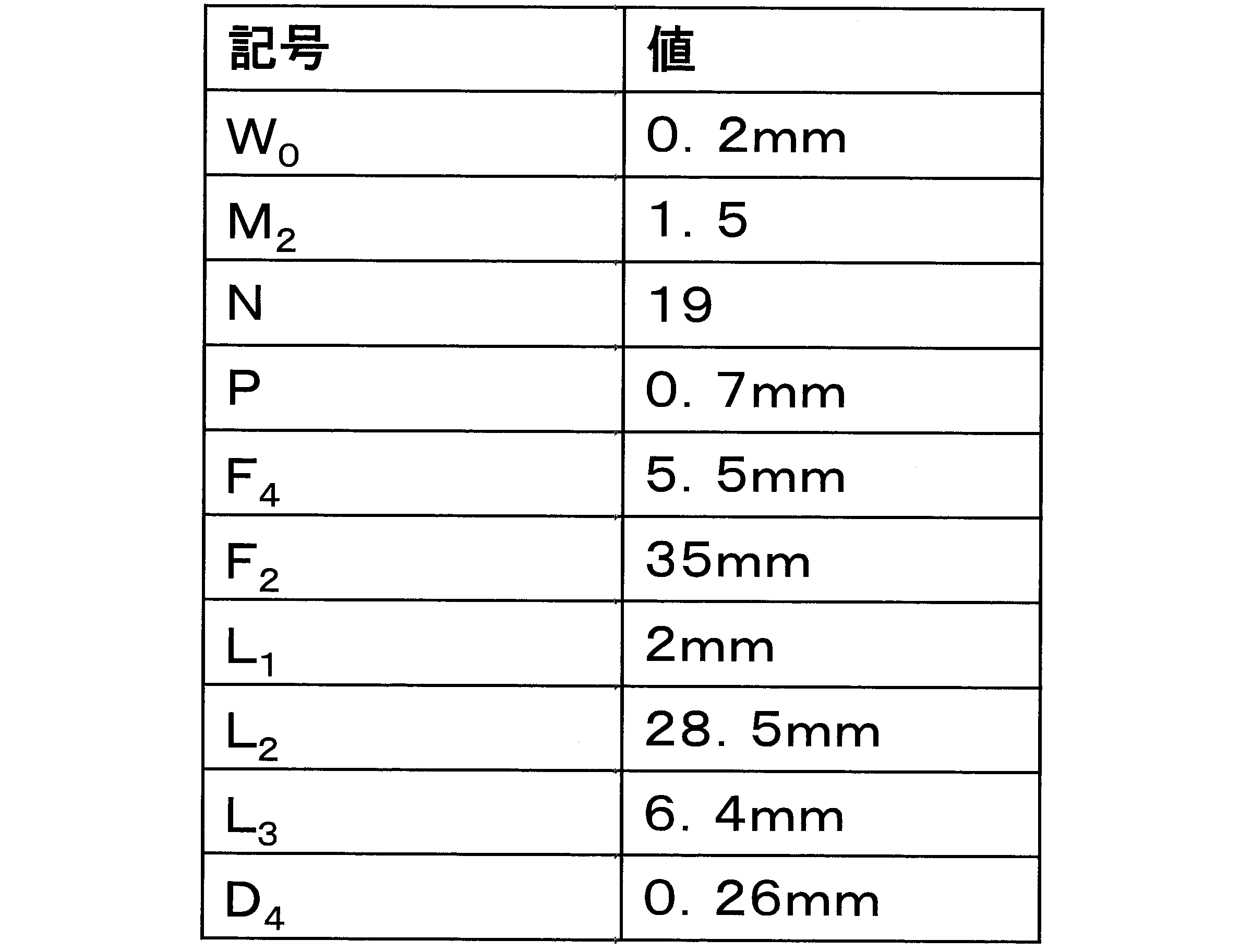
- Table 1 shows a first example of the specifications of the multiplexing optical system 100.
- the light emitting elements 11 of the light source 1 are arranged in a hexagonal lattice.
- the characteristics of the multiplexing optical system 100 are as follows.
- the size of the focused spot is approximately 48 ⁇ m in diameter.
- the NA when condensing light is about 0.13.
- An example of the characteristics of the optical fiber 5 is as follows.
- the core diameter of the optical fiber 5 is, for example, about 50 ⁇ m.
- Table 2 shows a second example of the specifications of the multiplexing optical system 100.
- the plurality of light emitting elements 11 of the light source 1 are arranged in a hexagonal lattice.
- the characteristics of the multiplexing optical system 100 are as follows.
- the size of the converging spot is about 44 ⁇ m in diameter.
- the NA at the time of condensing light is about 0.1.
- An example of the characteristics of the optical fiber 5 is as follows.
- the core diameter of the optical fiber 5 is, for example, about 50 ⁇ m.
- the multiplexing optical system 100 includes the light source, the optical path changing member, and the light collecting member.
- the light source includes a plurality of light emitting elements.
- the light emitting device is a two-dimensional photonic crystal surface emitting laser.
- the optical path changing member changes the optical path of each laser beam emitted from the plurality of light emitting elements and focuses the laser beam toward one point.
- the optical path changing member changes the optical path of each laser beam emitted from the plurality of light emitting elements and focuses the laser beam.
- the condensing member converges each laser beam emitted from the optical path changing member by a plurality of lens areas to form a combined beam.
- the multiplexing optical system 100 is a multiplexing optical system having high light-collecting properties.
- the multiplexing optical system 100 is a high-power multiplexing optical system.
- the condensing member is disposed at a position where the outermost diameters of adjacent laser beams emitted from the optical path changing member are in contact with each other. Thereby, the condensing property of the combined beam is further enhanced.
- the sizes of the plurality of lens regions included in the light collecting member are determined so as to be equal to the beam diameter of each laser beam incident on the plurality of lens regions.
- the laser beams emitted from the light focusing member are emitted with their outermost diameters in contact with each other. Thereby, the condensing property of the combined beam is further enhanced.
- the optical paths of the plurality of laser beams can be accurately changed by simple means.
- the ineffective area between each lens area can be minimized and laser beams can be made closer to each other. For this reason, the convergence of the combined beam can be improved.
- the plurality of light emitting elements are arranged in a hexagonal lattice.
- the plurality of light emitting elements are arranged most densely. Therefore, the plurality of laser beams that are the source of the combined beam enter the optical path changing member as close as possible. This also makes it possible to easily obtain a multiplexed beam having a high condensing property.
- "dense" generally indicates a state in which the objects are densely packed.
- FIG. 4 is a diagram showing an arrangement of the light emitting elements 11 included in the light source 201 in the multiplexing optical system according to Embodiment 2 of the present invention.
- FIG. 5 is a diagram showing an array of lens regions 240 in the lens array 204 according to the second embodiment.
- the light source 201 includes 16 light emitting elements 11.
- the 16 light emitting elements 11 are arranged in a square lattice on the surface 31 of the heat sink 3.
- the surface 31 is, for example, a single surface.
- the arrangement of the light emitting elements 11 is a hexagonal lattice pattern due to various limitations such as the performance of the device used when the light emitting elements 11 are arranged, the electrode structure of the light source 1 and the required number of light emitting elements 11.
- the beam occupancy can be increased to a certain extent to improve the condensing property of the combined beam.
- FIG. 6 is a diagram showing an arrangement of the light emitting elements 11 included in the light source 301 in the multiplexing optical system according to Embodiment 3 of the present invention.
- FIG. 7 is a diagram showing an array of lens regions 340 in the lens array 304 according to the third embodiment.
- the light source 301 includes ten light emitting elements 11.
- the ten light emitting elements 11 are arranged at equal angles on the circumference on the surface 31 of the heat sink 3.
- the surface 31 is, for example, a single surface.
- the beam occupancy obtained by the equiangular arrangement on the circumference according to the third embodiment is lower than the beam occupancy obtained by the hexagonal lattice arrangement according to the first embodiment.
- the beam occupancy is higher in FIG. 7 than in FIG.
- the arrangement of the light emitting elements 11 is a hexagonal lattice-like arrangement due to various limitations such as the performance of the device used for arranging the light emitting elements 11, the electrode structure of the light source 1, and the required number of light emitting elements 11.
- the beam occupancy can be increased to a certain extent to improve the condensing property of the combined beam.
- FIG. 8 is a diagram showing a cross section of a plane including the optical axis A in the multiplexing optical system 400 according to Embodiment 4 of the present invention.
- the multiplexing optical system 400 includes the light source 1, the polyhedral prism 402, and the lens array 4.
- the multiplexing optical system 400 can include the optical fiber 5.
- a polyhedral prism 402 is used instead of the lens 2 of the first embodiment. Except for this point, the multiplexing optical system 400 is the same as or similar to the multiplexing optical system 100. Therefore, the same or similar components as those of the multiplexing optical system 100 are denoted by the same reference numerals and description thereof will be omitted.
- the distance from the polygon prism 402 to the lens array 4 is L402 .
- the distance from the lens array 4 to the incident surface 51 of the optical fiber 5 is represented by L403 .
- the polyhedral prism 402 is arranged between the light source 1 and the lens array 4.
- the polyhedral prism 402 has a prism surface Pn corresponding to each of the plurality of light emitting elements 11.
- the subscript n is to corresponds with index n of the central ray A n. That is, the subscript n of the prism surface P n is the same as the index n of the central ray A n.
- the polyhedral prism 402 has an entrance surface 421 and an exit surface 422.
- the incident surface 421 of the polyhedral prism 402 is a plane perpendicular to the optical axis A of the multiplexing optical system 400.
- the exit surface 422 of the polyhedral prism 402 includes a prism surface Pn .
- the prism surfaces Pn are surfaces in different directions corresponding to the N light-emitting elements 11, respectively.
- Position of the optical axis A of the focal length F 402 polyhedral prism 402 is a focusing position.
- the condensing position is the center 50 of the incident surface 51 of the optical fiber 5.
- Each laser beam emitted from each light emitting element 11 is perpendicularly incident on the incident surface 421 of the polyhedral prism 402.
- Each laser beam entering the polyhedral prism 402 exits from the corresponding prism surface Pn .
- Each laser beam emitted from the polyhedral prism 402 proceeds toward the above-mentioned condensing position. If when the lens array 4 is not present, the central ray A n of each laser beam emitted from the polyhedron prism 402 is mainly collected at 50 of the incident surface 51 of the optical fiber 5.
- adjacent laser beams approach each other as they travel. Then, at a distance L 402 from polyhedral prism 402, the outermost diameter of the adjacent laser beam is in contact with one another.
- a lens array 4 is disposed.
- the lens array 4 is arranged at a position where the outermost diameters of adjacent laser beams emitted from the polyhedral prism 402 are in contact with each other. Then, each laser beam enters each corresponding lens area 40 of the lens array 4.
- Each laser beam passes through the lens array 4 with the energy loss minimized.
- Each laser beam transmitted through the lens array 4 is condensed at the center 50 of the incident surface 51 of the optical fiber 5 to become a combined beam, where energy is concentrated.
- the conditions of the multiplexing optical system 400 are set such that the sum of the distance L 402 and the distance L 403 is equal to the focal length F 402 .
- the conditions of the multiplexing optical system 400 include, for example, the focal point distance F 402 , the focal length F 404 of the lens array 4, the distance L 401 , the distance L 402 , the distance L 403 , and the like.
- the conditions of the multiplexing optical system 400 are set according to the characteristics of the light source 1 and the characteristics of the multiplexed beam to be obtained. In this manner, similarly to the first embodiment, it is possible to obtain a multiplexed beam having high condensing properties.
- the incident surface 421 of the polyhedral prism 402 does not have to be flat.
- the entrance surface may be a polyhedron.
- the optical path changing member according to the present invention is the lens 2 in the first to third embodiments, and is the polyhedral prism 402 in the fourth embodiment.
- the optical path changing member is not limited to these two.
- a diffractive optical element can be used as the optical path changing member. By using the diffractive optical element, the thickness of the optical path changing member can be reduced.
- FIG. 9 is a diagram illustrating a state of focusing of a laser beam transmitted through the lens array 4 when the shape of the lens array 4 in the first embodiment is not appropriate.
- the lens region 40R 1 on the optical axis A of the multiplexing optical system 100, a lens region 40R 2 and 40R 3 out of the optical axis A are all Have the same shape and are on the same plane.
- the laser beam transmitted through the lens region 40R 1 on the optical axis A form a minimum spot on the incident surface 51 of the optical fiber 5.
- the laser beam transmitted through the optical axis A outside the lens region 40R 2 and 40R 3 forms a minimum spot in front than to reach the incident surface 51.
- the laser beams do not intersect at one point but intersect.
- a method of correcting these aberrations As a method of correcting these aberrations, a method of combining a plurality of lenses or making a lens surface aspherical is known.
- a method of correcting aberration using a plurality of lenses is not suitable. This is because the lens array is an expensive optical member, and it is necessary to adjust the relative positions of the plurality of lens arrays with high accuracy.
- the curvature of field is an aberration that cannot be corrected by a single lens.
- the shape of the lens array refers to the shape and thickness of both surfaces in each lens region and the relative position of each lens region in the lens array. In order to obtain the same magnification in any of the lens regions, the focal length of each lens region should be equal.
- FIG. 10 is a diagram illustrating a first example of a suitable shape of the lens array 4 according to the first embodiment.
- each lens area 40 of the lens array 4 is parallel to the optical axis A of the multiplexing optical system 100.
- Each of the lens regions 40 has at least one lens surface, here a lens surface on the light source side, which is aspherical, and corrects aberrations other than field curvature.
- the optical axis A outside the lens region 40R 2 and 40R 3 inhibit astigmatism and coma. If both surfaces of each lens area 40 are aspherical, aberrations may be better corrected.
- the lens surfaces on the light source side in the lens regions 40R 1 , 40R 2 and 40R 3 are denoted by S1 R1 , S1 R2 and S1 R3 , respectively. Further, the lens surfaces on the converging point side in the lens regions 40R 1 , 40R 2 and 40R 3 are denoted by S2 R1 , S2 R2 and S2 R3 , respectively.
- curvatures C 2R1 , C 2R2 and C 2R3 are designed so as to satisfy the following relational expression.
- the curvature of the lens surface on the converging point side of each lens area 40 is designed to increase as the distance between the optical axis of the lens area and the optical axis A of the multiplexing optical system 100 increases. .
- the back focus can be increased by increasing the curvature of each lens surface on the focusing point side.
- the distance from the lens surface on the light-converging point side to the light-condensing position becomes longer as the lens area 40 is farther from the optical axis A of the multiplexing optical system 100. That is, by increasing the curvature of the lens surface closer to the converging point as the lens area 40 is farther away from the optical axis A of the multiplexing optical system 100, the extension of the back focus and the forward tilt of the converging position due to the curvature of field are reduced. Can be offset. As a result, the laser beam transmitted through each lens area 40 forms a minimum spot at the same location.
- the front focus becomes short.
- the distance L 2 is several tens of times larger several times the distance L 3. For this reason, the influence of the front focus changing by a very small distance about the curvature of field is small.
- the shape of the lens array 4 as described above, it is possible to correct aberration and obtain a good condensed spot, and to align the position where the minimum spot is formed, thereby improving the condensing property of the combined beam. be able to.
- FIG. 11 is a diagram illustrating a second example of a suitable shape of the lens array 4 according to the first embodiment.
- each lens region 40 of the lens array 4 is parallel to the optical axis A of the multiplexing optical system 100. Further, each lens region 40 has the same shape. That is, in each of the lens regions 40, the shape of the lens surface on the light source side is all the same, and the shape of the lens surface on the condensing point side is also all the same.
- each lens area 40 at least one lens surface, here the lens surface on the light source side, is aspherical, and corrects aberrations other than field curvature.
- the lens area is arranged at a position shifted toward the light-converging point along the optical axis A of the multiplexing optical system 100.
- the longer the distance between the optical axis of the lens area and the optical axis A of the multiplexing optical system 100 is, the longer the vertex of the lens surface on the converging point side of each lens area 40 is. It is located on the converging point side along the optical axis A. Thereby, the forward tilt of the image plane due to the field curvature is corrected.
- the distance between the lens region 40 and the lens 2 is slightly reduced by protruding the lens region 40 closer to the converging point as the lens region 40 is closer to the periphery.
- the effect of this is slight.
- the shape of the lens array 4 as described above, it is possible to correct aberration and obtain a good condensed spot, and to align the position where the minimum spot is formed, thereby improving the condensing property of the combined beam. be able to.
Landscapes
- Physics & Mathematics (AREA)
- General Physics & Mathematics (AREA)
- Optics & Photonics (AREA)
- Condensed Matter Physics & Semiconductors (AREA)
- Electromagnetism (AREA)
- Optical Couplings Of Light Guides (AREA)
- Semiconductor Lasers (AREA)
Abstract
Description
合波光学系では、光源に含まれる複数の発光素子からそれぞれ出射されるレーザー光線を合波することによって、高出力の合波ビームを形成する。この際、先述したように、合波ビームが高い集光性を有することが重要である。
<合波光学系100の構成>
図1は、本発明の実施の形態1に係る合波光学系100の構成を示す図である。図1は、合波光学系100の光軸Aを含む断面を示している。以下、図1を参照して、合波光学系100の全体構成を説明する。
次に、本実施の形態1で用いる2次元フォトニック結晶面発光レーザーについて説明する。2次元フォトニック結晶面発光レーザーは、活性層近傍に発振波長程度の周期的な構造を設けた面発光型の半導体レーザーである。この周期的な構造をフォトニック結晶構造という。
半導体レーザーを高出力かつ良好に動作させるためには、発熱への対処が重要である。半導体レーザーでは、供給電力の40~60%が熱になる。そして、出力が高くなると発生する熱がさらに増加する。そのため、高出力の半導体レーザーの発光素子は、サブマウントまたはヒートシンクを備える冷却構造の上に実装されることが好ましい。
次に、本実施の形態1に係る合波光学系100の動作について詳細に説明する。図2のように、合波光学系100は、間隔を空けて配列された複数の発光素子11から出射された複数のレーザー光線を集光させて合波ビームを形成する。この場合には、合波ビームの径内におけるビーム占有率を高めることによって、合波ビームの集光性が高められる。
光ファイバ5は、自身の入射面51の中心50と、複数の発光素子11から出射された各レーザー光線が1点に集光して合波ビームが形成される位置とが、一致するように配置されている。光ファイバ5の入射面51の中心50と、複数の発光素子11から出射された各レーザー光線が集光して合波ビームが形成される位置とは一致している。
次に、本実施の形態1に係る合波光学系100における具体的な数値例を示す。
表1は、合波光学系100の仕様の第1の例を示している。なお、光源1の複数の発光素子11は、六方格子状に配置されている。

表2は、合波光学系100の仕様の第2の例を示している。光源1の複数の発光素子11は、六方格子状に配置されている。
以上説明したように、本発明の実施の形態1に係る合波光学系100は、光源、光路変更部材および集光部材を備えている。光源は、複数の発光素子を含む。発光素子は2次元フォトニック結晶面発光レーザーである。光路変更部材は、複数の発光素子から出射された各レーザー光線の光路を変更して1点に向けて集光させる。光路変更部材は、複数の発光素子から出射された各レーザー光線の光路を変更して集光させる。集光部材は、光路変更部材から出射した各レーザー光線を複数のレンズ領域によって集光させて合波ビームを形成する。
<正方格子状の配列>
図4は、本発明の実施の形態2に係る合波光学系における、光源201に含まれる発光素子11の配列を示す図である。また、図5は、本実施の形態2に係るレンズアレイ204におけるレンズ領域240の配列を示す図である。
<円弧状の配列>
図6は、本発明の実施の形態3に係る合波光学系における、光源301に含まれる発光素子11の配列を示す図である。また、図7は、本実施の形態3に係るレンズアレイ304におけるレンズ領域340の配列を示す図である。
<多面体プリズム>
図8は、本発明の実施の形態4に係る合波光学系400における、光軸Aを含む面の断面を示す図である。
最後に、先述した実施の形態1におけるレンズアレイ4の形状の設計方法について、補足説明する。実施の形態1において、合波ビームの集光性を高めるためには、レンズアレイ4およびレンズアレイ4に含まれる各レンズ領域40のレンズ面の形状を、適切に設計する必要がある。なお、以下に説明する設計方法は、実施の形態2~4においても、同様に適用することができる。
図10は、実施の形態1におけるレンズアレイ4の好適な形状の第1の例を示す図である。
図11は、実施の形態1におけるレンズアレイ4の好適な形状の第2の例を示す図である。
Claims (16)
- 面発光レーザーの複数の発光素子を含む光源と、
前記複数の発光素子の各々から出射されたレーザー光線の光路をそれぞれ変更して集光させる光路変更部材と、
前記光路変更部材によって変更された複数の前記レーザー光線のそれぞれの光路に対応して配列された複数のレンズ領域を含み、該複数のレンズ領域によって前記複数のレーザー光線を集光させて合波ビームを形成する集光部材と
を備える、合波光学系。 - 前記集光部材は、前記光路変更部材から出射した隣り合うレーザー光線の最外径が互いに接するようになる位置に配置される、請求項1に記載の合波光学系。
- 前記集光部材に含まれる前記複数のレンズ領域の大きさは、該複数のレンズ領域に入射する前記複数のレーザー光線の最外径と等しくなるように定められ、
前記集光部材から出射する前記複数のレーザー光線は、隣り合うレーザー光線同士の最外径が互いに接する状態で出射される、請求項2に記載の合波光学系。 - 前記光路変更部材は、前記光源と前記集光部材との間に配置されたレンズである、請求項3に記載の合波光学系。
- 前記光路変更部材は、前記光源と前記集光部材との間に配置された多面体プリズムである、請求項3に記載の合波光学系。
- 前記光路変更部材は、前記光源と前記集光部材との間に配置された回折光学素子である、請求項3に記載の合波光学系。
- 前記集光部材は、前記複数のレンズ領域を含むレンズアレイである、請求項3~6のいずれか一項に記載の合波光学系。
- 前記複数のレンズ領域において、各レンズ領域の光軸は、前記合波光学系の光軸と平行である、請求項7に記載の合波光学系。
- 前記複数のレンズ領域において、各レンズ領域の少なくとも一方のレンズ面は非球面である、請求項7または8に記載の合波光学系。
- 前記複数のレンズ領域において、各レンズ領域の集光点側のレンズ面の曲率は、該レンズ領域の光軸と前記合波光学系の光軸との距離に依存して異なっている、請求項7~9のいずれか一項に記載の合波光学系。
- 前記複数のレンズ領域において、各レンズ領域の集光点側のレンズ面の曲率は、該レンズ領域の光軸と前記合波光学系の光軸との距離が長いほど大きい、請求項10に記載の合波光学系。
- 前記複数のレンズ領域において、各レンズ領域の集光点側のレンズ面の面頂点は、該レンズ領域の光軸と前記合波光学系の光軸との距離に依存して、前記合波光学系の光軸に沿った方向の位置が異なる、請求項7~9のいずれか一項に記載の合波光学系。
- 前記複数のレンズ領域において、各レンズ領域の集光点側のレンズ面の面頂点は、該レンズ領域の光軸と前記合波光学系の光軸との距離が長いほど、前記合波光学系の光軸に沿って集光点側に位置する、請求項12に記載の合波光学系。
- 前記複数の発光素子は六方格子状に配列されている、請求項3~13のいずれか一項に記載の合波光学系。
- 前記集光部材によって形成された前記合波ビームが入射面から入射して内部を伝送する光ファイバをさらに備え、
前記光ファイバはラージモードエリアファイバである、請求項3~14のいずれか一項に記載の合波光学系。 - 前記面発光レーザーは、2次元フォトニック結晶面発光レーザーである、請求項1~15のいずれか一項に記載の合波光学系。
Priority Applications (4)
| Application Number | Priority Date | Filing Date | Title |
|---|---|---|---|
| DE112019004655.1T DE112019004655B4 (de) | 2018-09-18 | 2019-09-13 | Optisches Multiplexsystem |
| US17/273,319 US11822125B2 (en) | 2018-09-18 | 2019-09-13 | Multiplexing optical system |
| CN201980059313.5A CN112673294B (zh) | 2018-09-18 | 2019-09-13 | 复用光学系统 |
| JP2020515781A JP6808892B2 (ja) | 2018-09-18 | 2019-09-13 | 合波光学系 |
Applications Claiming Priority (2)
| Application Number | Priority Date | Filing Date | Title |
|---|---|---|---|
| JP2018-173754 | 2018-09-18 | ||
| JP2018173754 | 2018-09-18 |
Publications (1)
| Publication Number | Publication Date |
|---|---|
| WO2020059664A1 true WO2020059664A1 (ja) | 2020-03-26 |
Family
ID=69887378
Family Applications (1)
| Application Number | Title | Priority Date | Filing Date |
|---|---|---|---|
| PCT/JP2019/036144 Ceased WO2020059664A1 (ja) | 2018-09-18 | 2019-09-13 | 合波光学系 |
Country Status (5)
| Country | Link |
|---|---|
| US (1) | US11822125B2 (ja) |
| JP (2) | JP6808892B2 (ja) |
| CN (1) | CN112673294B (ja) |
| DE (1) | DE112019004655B4 (ja) |
| WO (1) | WO2020059664A1 (ja) |
Cited By (2)
| Publication number | Priority date | Publication date | Assignee | Title |
|---|---|---|---|---|
| CN115267740A (zh) * | 2021-04-30 | 2022-11-01 | 上海禾赛科技有限公司 | 发光装置及其形成方法、激光雷达 |
| JP7696146B1 (ja) | 2024-02-20 | 2025-06-20 | Dmg森精機株式会社 | 付加加工用ヘッドおよび加工機械 |
Families Citing this family (4)
| Publication number | Priority date | Publication date | Assignee | Title |
|---|---|---|---|---|
| CN113260890B (zh) * | 2018-12-13 | 2024-06-11 | 索尼集团公司 | 光学连接器、光缆和电子设备 |
| CN115327786B (zh) * | 2021-09-02 | 2025-10-14 | 神盾股份有限公司 | 光学系统及光学感测模块 |
| CN115799993A (zh) * | 2022-12-16 | 2023-03-14 | 湖北华中长江光电科技有限公司 | 一种多路激光阵列密排发射装置 |
| WO2026028487A1 (ja) * | 2024-07-31 | 2026-02-05 | ソニーセミコンダクタソリューションズ株式会社 | フォトニック結晶面発光素子及び発光装置 |
Citations (7)
| Publication number | Priority date | Publication date | Assignee | Title |
|---|---|---|---|---|
| JP2005114977A (ja) * | 2003-10-07 | 2005-04-28 | Ricoh Opt Ind Co Ltd | 光パワー合成用光学系および光源モジュール |
| WO2012053167A1 (ja) * | 2010-10-19 | 2012-04-26 | パナソニック株式会社 | 光合波装置及びプロジェクタ |
| WO2016129323A1 (ja) * | 2015-02-09 | 2016-08-18 | 三菱電機株式会社 | レーザモジュールおよびレーザ加工装置 |
| JP2017026660A (ja) * | 2015-07-16 | 2017-02-02 | 住友金属鉱山株式会社 | 光ファイバ端末 |
| JP2017117891A (ja) * | 2015-12-22 | 2017-06-29 | 株式会社リコー | 光学センサ、光学検査装置、及び光学特性検出方法 |
| JP2017212321A (ja) * | 2016-05-25 | 2017-11-30 | 株式会社リコー | 面発光レーザ、面発光レーザアレイ、光源ユニット及びレーザ装置 |
| US20180239096A1 (en) * | 2015-08-10 | 2018-08-23 | Multiphoton Optics Gmbh | Optical component with beam deflection element, method for production thereof, and beam deflection elements suitable for the component |
Family Cites Families (18)
| Publication number | Priority date | Publication date | Assignee | Title |
|---|---|---|---|---|
| US5333077A (en) | 1989-10-31 | 1994-07-26 | Massachusetts Inst Technology | Method and apparatus for efficient concentration of light from laser diode arrays |
| JPH0876054A (ja) * | 1993-12-28 | 1996-03-22 | Fuji Photo Film Co Ltd | レーザ装置 |
| JP2000022643A (ja) * | 1998-07-01 | 2000-01-21 | Canon Inc | 光インタコネクトシステム |
| JP2002202442A (ja) | 2000-11-06 | 2002-07-19 | Fuji Photo Film Co Ltd | 合波レーザー光源および露光装置 |
| US7076129B2 (en) * | 2003-04-30 | 2006-07-11 | Lemoff Brian E | Apparatus and method for a filterless parallel WDM multiplexer |
| US7357530B2 (en) * | 2005-07-15 | 2008-04-15 | Bwt Property, Inc. | Lighting apparatus for navigational aids |
| JP2007248581A (ja) | 2006-03-14 | 2007-09-27 | Sumitomo Electric Ind Ltd | レーザーモジュール |
| JP4776498B2 (ja) | 2006-07-14 | 2011-09-21 | 富士通株式会社 | レンズアレイを用いた光学装置 |
| US20080225257A1 (en) * | 2007-03-13 | 2008-09-18 | Nikon Corporation | Optical integrator system, illumination optical apparatus, exposure apparatus, and device manufacturing method |
| US7615737B2 (en) * | 2007-05-08 | 2009-11-10 | The Boeing Company | High precision compact rotation angle absolute encoder |
| JP2008281829A (ja) * | 2007-05-11 | 2008-11-20 | Konica Minolta Opto Inc | 照明光学系 |
| CN102742100B (zh) * | 2009-08-20 | 2015-06-03 | 皇家飞利浦电子股份有限公司 | 具有可配置强度分布的激光器装置 |
| JP5831403B2 (ja) | 2011-09-01 | 2015-12-09 | コニカミノルタ株式会社 | 結合光学系及び結合方法 |
| DE102012202177B3 (de) | 2012-02-14 | 2012-12-27 | Trumpf Laser Gmbh + Co. Kg | Freistrahloptische Faser-zu-Faser-Kopplungsvorrichtung |
| CN103219648B (zh) | 2013-04-11 | 2015-08-26 | 中北大学 | 一种激光光源的光纤耦合系统 |
| JP2015153889A (ja) * | 2014-02-14 | 2015-08-24 | 三菱電機株式会社 | レーザ合成光学装置 |
| JPWO2016080252A1 (ja) * | 2014-11-20 | 2017-08-31 | カナレ電気株式会社 | 外部共振器型半導体レーザ |
| CN107615601B (zh) | 2015-05-27 | 2019-11-08 | 三菱电机株式会社 | 激光模块及激光加工装置 |
-
2019
- 2019-09-13 CN CN201980059313.5A patent/CN112673294B/zh active Active
- 2019-09-13 US US17/273,319 patent/US11822125B2/en active Active
- 2019-09-13 WO PCT/JP2019/036144 patent/WO2020059664A1/ja not_active Ceased
- 2019-09-13 JP JP2020515781A patent/JP6808892B2/ja active Active
- 2019-09-13 DE DE112019004655.1T patent/DE112019004655B4/de active Active
-
2020
- 2020-12-09 JP JP2020204010A patent/JP7086501B2/ja active Active
Patent Citations (7)
| Publication number | Priority date | Publication date | Assignee | Title |
|---|---|---|---|---|
| JP2005114977A (ja) * | 2003-10-07 | 2005-04-28 | Ricoh Opt Ind Co Ltd | 光パワー合成用光学系および光源モジュール |
| WO2012053167A1 (ja) * | 2010-10-19 | 2012-04-26 | パナソニック株式会社 | 光合波装置及びプロジェクタ |
| WO2016129323A1 (ja) * | 2015-02-09 | 2016-08-18 | 三菱電機株式会社 | レーザモジュールおよびレーザ加工装置 |
| JP2017026660A (ja) * | 2015-07-16 | 2017-02-02 | 住友金属鉱山株式会社 | 光ファイバ端末 |
| US20180239096A1 (en) * | 2015-08-10 | 2018-08-23 | Multiphoton Optics Gmbh | Optical component with beam deflection element, method for production thereof, and beam deflection elements suitable for the component |
| JP2017117891A (ja) * | 2015-12-22 | 2017-06-29 | 株式会社リコー | 光学センサ、光学検査装置、及び光学特性検出方法 |
| JP2017212321A (ja) * | 2016-05-25 | 2017-11-30 | 株式会社リコー | 面発光レーザ、面発光レーザアレイ、光源ユニット及びレーザ装置 |
Cited By (3)
| Publication number | Priority date | Publication date | Assignee | Title |
|---|---|---|---|---|
| CN115267740A (zh) * | 2021-04-30 | 2022-11-01 | 上海禾赛科技有限公司 | 发光装置及其形成方法、激光雷达 |
| JP7696146B1 (ja) | 2024-02-20 | 2025-06-20 | Dmg森精機株式会社 | 付加加工用ヘッドおよび加工機械 |
| JP2025127208A (ja) * | 2024-02-20 | 2025-09-01 | Dmg森精機株式会社 | 付加加工用ヘッドおよび加工機械 |
Also Published As
| Publication number | Publication date |
|---|---|
| JP2021064794A (ja) | 2021-04-22 |
| CN112673294A (zh) | 2021-04-16 |
| JP6808892B2 (ja) | 2021-01-06 |
| DE112019004655B4 (de) | 2025-07-10 |
| JPWO2020059664A1 (ja) | 2021-01-07 |
| US11822125B2 (en) | 2023-11-21 |
| CN112673294B (zh) | 2022-06-24 |
| DE112019004655T5 (de) | 2021-07-01 |
| JP7086501B2 (ja) | 2022-06-20 |
| US20210318493A1 (en) | 2021-10-14 |
Similar Documents
| Publication | Publication Date | Title |
|---|---|---|
| JP7086501B2 (ja) | 合波光学系 | |
| US6504975B1 (en) | Coupling lens and semiconductor laser module | |
| KR101893235B1 (ko) | 디스크 레이저용 펌프 광 조립체 | |
| CN109073908B (zh) | 平行光发生装置 | |
| US9746681B2 (en) | Laser beam combining device | |
| US9541721B2 (en) | Laser device | |
| JP2015072955A (ja) | スペクトルビーム結合ファイバレーザ装置 | |
| JP5935465B2 (ja) | 光学装置 | |
| US11249317B2 (en) | Device for collimating a light beam, high-power laser, and focusing optical unit and method for collimating a light beam | |
| CN112310800A (zh) | 一种紧凑式光纤耦合输出半导体激光器 | |
| US20050078383A1 (en) | Plastic, thermally stable, laser diode coupler | |
| JP4048016B2 (ja) | 半導体レーザ光源及びこれを用いた半導体レーザ加工装置 | |
| KR20210027397A (ko) | 다파장 광학 시스템 및 레이저 어닐링 장치 | |
| JP2005157358A (ja) | 特に高出力ダイオード・レーザに対するビーム整形のための屈折性・回折性ハイブリッド型レンズ | |
| CN114859640A (zh) | 一种光整形系统、光源装置以及光源装置的设计方法 | |
| JP7154669B1 (ja) | 細径ビーム生成装置 | |
| JP7739942B2 (ja) | レーザ装置 | |
| RU2714781C1 (ru) | Способ поперечной накачки рабочей среды лазера | |
| JP7151497B2 (ja) | 光源装置 | |
| JP6693680B2 (ja) | 平行光発生装置 | |
| JPH06324202A (ja) | 集光用レンズおよび集光用レンズアレイ | |
| CN117543320A (zh) | 紧凑化激光输出方法、激光输出头和激光器件 | |
| CN119846850A (zh) | 一种空间激光合束器及激光器 | |
| WO2012001413A1 (en) | Fibre optical coupling |
Legal Events
| Date | Code | Title | Description |
|---|---|---|---|
| ENP | Entry into the national phase |
Ref document number: 2020515781 Country of ref document: JP Kind code of ref document: A |
|
| 121 | Ep: the epo has been informed by wipo that ep was designated in this application |
Ref document number: 19861514 Country of ref document: EP Kind code of ref document: A1 |
|
| 122 | Ep: pct application non-entry in european phase |
Ref document number: 19861514 Country of ref document: EP Kind code of ref document: A1 |
|
| WWG | Wipo information: grant in national office |
Ref document number: 112019004655 Country of ref document: DE |