WO2020054786A1 - 光学フィルタおよび撮像装置 - Google Patents
光学フィルタおよび撮像装置 Download PDFInfo
- Publication number
- WO2020054786A1 WO2020054786A1 PCT/JP2019/035779 JP2019035779W WO2020054786A1 WO 2020054786 A1 WO2020054786 A1 WO 2020054786A1 JP 2019035779 W JP2019035779 W JP 2019035779W WO 2020054786 A1 WO2020054786 A1 WO 2020054786A1
- Authority
- WO
- WIPO (PCT)
- Prior art keywords
- group
- wavelength
- carbon atoms
- transmittance
- resin
- Prior art date
- Legal status (The legal status is an assumption and is not a legal conclusion. Google has not performed a legal analysis and makes no representation as to the accuracy of the status listed.)
- Ceased
Links
- 0 C*C(C1[C@]2*)(C(*)(*)*(C)=C1C(C(*)=C(*)*1C)=C1C2=C(C(*)=C1c2c(*)c(C(*)(*)C(*)(*3C)O*)c3c3c2*(C)C(*)=C3C)C1=O)N* Chemical compound C*C(C1[C@]2*)(C(*)(*)*(C)=C1C(C(*)=C(*)*1C)=C1C2=C(C(*)=C1c2c(*)c(C(*)(*)C(*)(*3C)O*)c3c3c2*(C)C(*)=C3C)C1=O)N* 0.000 description 1
- PWZJXVAMUSGOKL-UHFFFAOYSA-N CCCCC(CC)CN(CC(CC)CCCC)c1cc(C(c2c-3[s]c(C(C(/C4=C(\C=C5C(C6=C7)(c8ccccc8)c8ccccc8)/SC5=C6SC7=[N+](CC(CC)CCCC)CC(CC)CCCC)=O)=C4[O-])c2)(c2ccccc2)c2ccccc2)c-3[s]1 Chemical compound CCCCC(CC)CN(CC(CC)CCCC)c1cc(C(c2c-3[s]c(C(C(/C4=C(\C=C5C(C6=C7)(c8ccccc8)c8ccccc8)/SC5=C6SC7=[N+](CC(CC)CCCC)CC(CC)CCCC)=O)=C4[O-])c2)(c2ccccc2)c2ccccc2)c-3[s]1 PWZJXVAMUSGOKL-UHFFFAOYSA-N 0.000 description 1
Images
Classifications
-
- H—ELECTRICITY
- H10—SEMICONDUCTOR DEVICES; ELECTRIC SOLID-STATE DEVICES NOT OTHERWISE PROVIDED FOR
- H10F—INORGANIC SEMICONDUCTOR DEVICES SENSITIVE TO INFRARED RADIATION, LIGHT, ELECTROMAGNETIC RADIATION OF SHORTER WAVELENGTH OR CORPUSCULAR RADIATION
- H10F39/00—Integrated devices, or assemblies of multiple devices, comprising at least one element covered by group H10F30/00, e.g. radiation detectors comprising photodiode arrays
- H10F39/80—Constructional details of image sensors
- H10F39/806—Optical elements or arrangements associated with the image sensors
-
- C—CHEMISTRY; METALLURGY
- C09—DYES; PAINTS; POLISHES; NATURAL RESINS; ADHESIVES; COMPOSITIONS NOT OTHERWISE PROVIDED FOR; APPLICATIONS OF MATERIALS NOT OTHERWISE PROVIDED FOR
- C09B—ORGANIC DYES OR CLOSELY-RELATED COMPOUNDS FOR PRODUCING DYES, e.g. PIGMENTS; MORDANTS; LAKES
- C09B57/00—Other synthetic dyes of known constitution
- C09B57/007—Squaraine dyes
-
- C—CHEMISTRY; METALLURGY
- C09—DYES; PAINTS; POLISHES; NATURAL RESINS; ADHESIVES; COMPOSITIONS NOT OTHERWISE PROVIDED FOR; APPLICATIONS OF MATERIALS NOT OTHERWISE PROVIDED FOR
- C09B—ORGANIC DYES OR CLOSELY-RELATED COMPOUNDS FOR PRODUCING DYES, e.g. PIGMENTS; MORDANTS; LAKES
- C09B67/00—Influencing the physical, e.g. the dyeing or printing properties of dyestuffs without chemical reactions, e.g. by treating with solvents grinding or grinding assistants, coating of pigments or dyes; Process features in the making of dyestuff preparations; Dyestuff preparations of a special physical nature, e.g. tablets, films
- C09B67/006—Preparation of organic pigments
- C09B67/0063—Preparation of organic pigments of organic pigments with only macromolecular substances
-
- G—PHYSICS
- G02—OPTICS
- G02B—OPTICAL ELEMENTS, SYSTEMS OR APPARATUS
- G02B1/00—Optical elements characterised by the material of which they are made; Optical coatings for optical elements
- G02B1/04—Optical elements characterised by the material of which they are made; Optical coatings for optical elements made of organic materials, e.g. plastics
-
- G—PHYSICS
- G02—OPTICS
- G02B—OPTICAL ELEMENTS, SYSTEMS OR APPARATUS
- G02B5/00—Optical elements other than lenses
- G02B5/20—Filters
- G02B5/208—Filters for use with infrared or ultraviolet radiation, e.g. for separating visible light from infrared and/or ultraviolet radiation
-
- G—PHYSICS
- G02—OPTICS
- G02B—OPTICAL ELEMENTS, SYSTEMS OR APPARATUS
- G02B5/00—Optical elements other than lenses
- G02B5/20—Filters
- G02B5/22—Absorbing filters
- G02B5/223—Absorbing filters containing organic substances, e.g. dyes, inks or pigments
-
- H—ELECTRICITY
- H10—SEMICONDUCTOR DEVICES; ELECTRIC SOLID-STATE DEVICES NOT OTHERWISE PROVIDED FOR
- H10F—INORGANIC SEMICONDUCTOR DEVICES SENSITIVE TO INFRARED RADIATION, LIGHT, ELECTROMAGNETIC RADIATION OF SHORTER WAVELENGTH OR CORPUSCULAR RADIATION
- H10F39/00—Integrated devices, or assemblies of multiple devices, comprising at least one element covered by group H10F30/00, e.g. radiation detectors comprising photodiode arrays
- H10F39/80—Constructional details of image sensors
- H10F39/805—Coatings
Definitions
- the present invention relates to an optical filter that transmits light in a visible wavelength region and blocks light in a near-infrared wavelength region, and an imaging device including the optical filter.
- An imaging device using a solid-state imaging device transmits light in the visible region (hereinafter, also referred to as “visible light”) and transmits light in the near-infrared region (hereinafter, “near red”) in order to reproduce color tones and obtain a clear image.
- An optical filter that blocks external light is used.
- a near-infrared cut filter in which an absorption layer containing a near-infrared absorbing dye and a resin and a reflective layer made of a dielectric multilayer film that blocks near-infrared light are provided on a glass substrate. are known.
- Patent Literature 1 describes a near-infrared cut filter including a polyimide resin film containing a near-infrared absorber and a dielectric multilayer film. .
- Patent Document 2 further describes a near-infrared cut filter including a resin film containing a specific squarylium dye, a phthalocyanine dye and / or a cyanine dye, and a dielectric multilayer film.
- Patent Literature 3 describes a near-infrared cut filter including a transparent resin film containing a near-infrared absorber, particularly a norbornene resin film and a dielectric multilayer film.
- Patent Document 4 describes a near-infrared cut filter composed of a transparent resin film containing a near-infrared absorber and a dielectric multilayer film.
- Patent Document 5 discloses a near-infrared cut filter provided with an absorption layer containing a resin base material, a near-infrared absorbing dye, and a resin, and a reflective layer made of a dielectric multilayer film that blocks near-infrared light.
- the resin of the base material and the absorbing layer is selected from fluorinated aromatic polymer, poly (amide) imide resin, polyamide resin, aramid resin and polycycloolefin resin. I have.
- JP 2013-29708 A Japanese Patent Application Laid-Open No. 2017-129881 Japanese Patent No. 5489669 WO 2014/192714 Japanese Patent No. 5706932
- the transmittance in the blue wavelength band is reduced due to the absorption of the film itself.
- a dye is added to a polyimide film having a thickness of 20 ⁇ m or more, high-temperature drying is required to volatilize a high-boiling solvent such as ⁇ -butyrolactone or N-methylpyrrolidone used in a polyimide varnish, and thus can be used.
- Dyes are limited to dyes that do not thermally degrade at the temperature at the time of drying (for example, phthalocyanine dyes), and it is difficult to provide an optical filter having excellent visible transmittance.
- Patent Document 2 exemplifies a cycloolefin polymer, polycarbonate, polyethersulfone, an acrylic resin and the like as a film substrate. It is hard to say that the resins specifically exemplified are sufficiently compatible in terms of transparency and glass transition temperature. When the glass transition temperature is low, the possibility of causing curl due to expansion and contraction of the film and cracking of the multilayer film formed on the film during the heating process increases.
- Patent Documents 3, 4, and 5 similarly have excellent visible transmittance, but no reports have been reported that are compatible with the glass transition temperature.
- the near-infrared cut filters of Patent Documents 1 to 5 all achieve a reduction in thickness, they have high transparency of visible light, high shielding of near-infrared light, and heat resistance of the optical characteristics. None is compatible.
- the present invention is a near-infrared cut filter using a resin material as a base material, having high transparency of visible light and high shielding property of near-infrared light, and an optical filter having excellent heat resistance of the optical characteristics, and It is an object of the present invention to provide an imaging device using the optical filter and having excellent color reproducibility and heat resistance.
- the optical filter according to one embodiment of the present invention, A resin base material having a thickness of 20 ⁇ m or more and 110 ⁇ m or less, An absorption layer having a thickness of 0.25 ⁇ m or more and 12 ⁇ m or less, which is disposed on at least one main surface of the resin base material; An optical filter having a dielectric multilayer film disposed as an outermost layer above both main surfaces of the resin base material, At least one of the dielectric multilayer films is a near-infrared reflective layer,
- the resin base material is mainly composed of a first transparent resin having a glass transition temperature of 170 ° C. or higher, and the first transparent resin has a wavelength of 350 to 1100 nm in a spectral transmittance curve at a thickness of 100 ⁇ m.
- the average internal transmittance of 350 to 450 nm is 95% or more, the minimum internal transmittance of 400 to 450 nm is 97% or more, and the wavelength at which the internal transmittance is 90% in the region of 500 nm or less is 350 nm or less.
- the absorption layer includes a near-infrared absorbing dye (A) and a second transparent resin having a glass transition temperature of 170 ° C. or higher, and a relationship between the near-infrared absorbing dye (A) and the second transparent resin. Satisfies the following (ii-1) and (ii-2).
- the present invention also provides an imaging device provided with the optical filter of the present invention.
- an optical filter having high transparency of visible light and high shielding property of near-infrared light, and having excellent heat resistance of the optical characteristics.
- an optical filter having resistance to thermal deformation in a high-temperature process and thermal degradation of a dye can be obtained.
- the stress of the dielectric multilayer film is likely to be applied to the substrate, and the dielectric multilayer film is formed from the substrate or the absorption layer using the resin material.
- the optical filter has high adhesion of the dielectric multilayer film to a substrate or an absorption layer using a resin material.
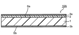
- FIG. 1 is a cross-sectional view schematically illustrating an example of an optical filter according to an embodiment.
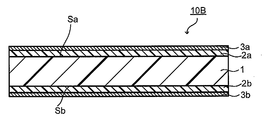
- FIG. 2 is a cross-sectional view schematically illustrating another example of the optical filter according to the embodiment.
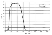
- FIG. 3 is a diagram illustrating a spectral transmittance curve of the optical filter of the example.
- NIR dye near-infrared absorbing dye
- UV dye ultraviolet absorbing dye
- the compound represented by the formula (I) is referred to as compound (I).
- the dye comprising the compound (I) is also referred to as dye (I), and the same applies to other dyes.
- a compound represented by the formula (A1) described below is referred to as a compound (A1)
- a dye including the compound is also referred to as a dye (A1).
- a group represented by the formula (1x) is also referred to as a group (1x), and the same applies to a group represented by another formula.
- the internal transmittance is a transmittance obtained by subtracting the influence of interfacial reflection from the actually measured transmittance, which is expressed by the formula of actually measured transmittance / (100 ⁇ reflectance).
- the transmittance of the resin substrate and the spectral distribution of the transmittance of the layer measured when the dye such as the absorbing layer is contained in the transparent resin are all referred to as “internal transmittance” even when described as “transmittance”. Rate ".
- the transmittance measured by dissolving the dye in a solvent such as dichloromethane, and the transmittance of an optical filter having a dielectric multilayer film are measured transmittances.
- the transmittance is, for example, 90% or more, which means that the transmittance does not fall below 90% in the entire wavelength region, that is, the minimum transmittance is 90% or more in the wavelength region.
- that the transmittance is, for example, 1% or less means that the transmittance does not exceed 1% in the entire wavelength region, that is, the maximum transmittance is 1% or less in the wavelength region.
- the average transmittance and the average internal transmittance in a specific wavelength range are the arithmetic average of the transmittance and the internal transmittance for each 1 nm in the wavelength range. In this specification, “to” indicating a numerical range includes upper and lower limits.
- An optical filter of one embodiment of the present invention (hereinafter, also referred to as “the present filter”) includes a resin substrate having the following configuration, and an absorbing layer having the following configuration disposed on at least one main surface of the resin substrate.
- a dielectric multilayer film disposed as an outermost layer on both main surfaces of the resin substrate, at least one of the dielectric multilayer films being a near-infrared reflective layer.
- the resin base material of the present filter is mainly composed of a first transparent resin having a thickness of 20 ⁇ m or more and 110 ⁇ m or less and a glass transition temperature of 170 ° C. or more.
- the first transparent resin has an average internal transmittance of 95% or more at a wavelength of 350 to 450 nm and a minimum internal transmittance of 97% at a wavelength of 400 to 450 nm in a spectral transmittance curve at a wavelength of 350 to 1100 nm when the thickness is 100 ⁇ m. % Or more, and the wavelength at which the internal transmittance becomes 90% in a region having a wavelength of 500 nm or less is 350 nm or less.
- the absorption layer in the present filter has a thickness of 0.25 ⁇ m or more and 12 ⁇ m or less, and contains an NIR dye (A) and a second transparent resin having a glass transition temperature of 170 ° C. or more.
- the relationship between the NIR dye (A) and the second transparent resin satisfies the following (ii-1) and (ii-2).
- the average internal transmittance T 435-500ave (A) TR of light in the wavelength range of 435-500 nm and the average internal transmittance T500-600ave (A) TR of light in the wavelength range of 500-600 nm are: Both are 94% or more.
- the NIR dye (A) preferably satisfies the following (i-1) and (i-2).
- (I-1) In a spectral transmittance curve at a wavelength of 400 to 800 nm measured by dissolving the NIR dye (A) in dichloromethane, the maximum absorption wavelength ⁇ max (A) DCM is in a wavelength region of 670 to 735 nm.
- (I-2) In a spectral transmittance curve at a wavelength of 350 to 1100 nm, which is measured by including the NIR dye (A) in dichloromethane so that the transmittance in a maximum absorption wavelength ⁇ max (A) DCM becomes 1%,
- the average transmittance at a wavelength of 435 to 500 nm (hereinafter, referred to as “T 435-500ave (A) DCM ”) is 94% or more, and the average transmittance at a wavelength of 500 to 600 nm (hereinafter, “T 500-600ave ” ).
- (A) DCM ”) is 94% or more.
- FIG. 1 and 2 are cross-sectional views schematically showing one example and another example of the optical filter according to one embodiment.
- the present filter may have the absorption layer on one main surface of the resin base material or on both main surfaces.
- the optical filter 10A shown in FIG. 1 is an example having the absorption layer 2 on one main surface Sa of the resin substrate 1, and the optical filter 10B shown in FIG. This is an example in which a first absorption layer 2a and a second absorption layer 2b are respectively provided on the main surface Sb.
- “having the absorption layer 2 on one main surface Sa (above or above) of the resin base material 1” is not limited to the case where the absorption layer 2 is provided in contact with the main surface Sa of the resin base material 1, The case where another functional layer is provided between the resin substrate 1 and the absorption layer 2 is also included. For other configurations, “having on the main surface (above or above)” has the same meaning.
- An optical filter 10A shown in FIG. 1 includes a resin base 1 having a first main surface Sa and a second main surface Sb opposed to each other, and an absorption filter disposed on the first main surface Sa of the resin base 1.
- Layer 2 a first dielectric multilayer film 3a disposed as an outermost layer on the absorption layer 2 on the first main surface Sa of the resin base material 1, and a second main surface Sb of the resin base material 1
- a second dielectric multilayer film 3b disposed as the outermost layer.
- the absorption layer 2 is a near-infrared absorption layer having the above-mentioned thickness containing the NIR dye (A) and the second transparent resin.
- the absorbing layer 2 may contain, in addition to the NIR dye (A), a dye that absorbs light in a wavelength region other than near infrared rays, for example, a UV dye.
- the other may or may not be a near-infrared reflective layer.
- the dielectric multilayer film other than the near-infrared reflective layer include an antireflection layer and a reflective layer that reflects a wavelength region other than near-infrared light.
- the near-infrared reflecting layer may reflect a wavelength region other than near-infrared light.
- the first dielectric multilayer film 3a and the second dielectric multilayer film 3b may be the same or different.
- each of the first dielectric multilayer film 3a and the second dielectric multilayer film 3b is a near-infrared reflective layer that reflects near-ultraviolet light and near-infrared light and has a property of transmitting visible light.
- the first dielectric multilayer film 3a reflects near-ultraviolet light and first near-infrared light
- the second dielectric multilayer film 3b reflects near-ultraviolet light and second near-infrared light. May be reflected.
- the optical filter 10B shown in FIG. 2 includes a resin base 1 having a first main surface Sa and a second main surface Sb opposed to each other, and a second filter disposed on the first main surface Sa of the resin base 1.
- the first dielectric multilayer film 3a disposed as the outermost layer and the second dielectric multilayer film disposed as the outermost layer on the second absorption layer 2b on the second main surface Sb of the resin substrate 1 3b.
- the resin substrate 1 has the above configuration.
- the first dielectric multilayer film 3a and the second dielectric multilayer film 3b can have the same configuration as the optical filter 10A.
- at least one of the first absorption layer 2a and the second absorption layer 2b is an absorption layer having the above configuration in the present filter.
- the absorption layer having the above configuration in the present filter contains a dye that absorbs light in a wavelength region other than near infrared rays, for example, a UV dye, in addition to the NIR dye (A), similarly to the absorption layer 2 of the optical filter 10A. Is also good.
- the first absorption layer 2a and the second absorption layer 2b may be the same or different.
- the first absorption layer 2a and the second absorption layer 2b are different from each other, for example, the first absorption layer 2a and the second absorption layer 2b are respectively provided with the near-infrared absorption layer and the transparent resin having the above configuration in the present filter. And an ultraviolet absorbing layer containing a UV dye.
- a dielectric multilayer film including a resin base material, an absorption layer, and a near-infrared reflection layer, which constitute the present filter will be described.
- the absorbing layer having the above thickness and containing the NIR dye (A) and the second transparent resin is simply referred to as “absorbing layer” unless otherwise specified.
- Absorption layers that do not satisfy these requirements are referred to as “other absorption layers”.
- the resin base material has, as a main component, a first transparent resin having a thickness of 20 ⁇ m or more and 110 ⁇ m or less and a glass transition temperature (hereinafter, also referred to as “Tg”) of 170 ° C. or more. Tg is determined by DSC measurement (Differential Scanning Calorimetry).
- Tg glass transition temperature
- the fact that the resin base material has the first transparent resin as a main component means that the ratio of the first transparent resin in the resin base material is 90% by mass or more. From the viewpoints of Tg and high transmittance of visible light, the resin base material preferably has a first transparent resin content of 95% by mass, particularly preferably the first transparent resin.
- the thickness of the resin substrate is 20 ⁇ m or more, the strength of the present filter is sufficient, and when the thickness is 110 ⁇ m or less, the present filter has high visible light transmittance.
- the thickness of the resin substrate is preferably at least 40 ⁇ m, more preferably at least 60 ⁇ m.
- the thickness of the resin substrate is preferably 100 ⁇ m or less, more preferably 90 ⁇ m or less.
- the first transparent resin has a Tg of 170 ° C. or higher, the resin base material is unlikely to be deformed by heat or stress, and the filter of the present invention is excellent in the adhesion of the dielectric multilayer film.
- Tg is preferably 200 ° C. or higher, more preferably 210 ° C. or higher.
- the Tg of the first transparent resin is preferably 400 ° C. or lower from the viewpoint of moldability and the like.
- the first transparent resin has an average internal transmittance at a wavelength of 350 to 450 nm (hereinafter, referred to as “ T350-450ave (TR) ”) of 95 in a spectral transmittance curve at a wavelength of 350 to 1100 nm when the thickness is 100 ⁇ m. % Or more, and the minimum internal transmittance at a wavelength of 400 to 450 nm (hereinafter referred to as “T 400-450 min (TR) ”) is 97% or more, and the internal transmittance is 90% at a wavelength of 500 nm or less.
- Wavelength hereinafter referred to as “ ⁇ uv90 ”
- T 350-450ave (TR) is 95% or more
- T 400-450 min (TR) is 97% or more
- ⁇ uv90 is 350 nm or less
- the present filter has high visible light transmittance.
- T 350-450ave is preferably at least 97%, more preferably at least 98%.
- T 400-450 min (TR) is preferably at least 97.5%, more preferably at least 98%.
- ⁇ uv90 is preferably 340 nm or less.
- the type of the first transparent resin is not particularly limited as long as the above requirements are satisfied.
- One or more types selected from a polyimide resin and a polycarbonate resin satisfying the above requirements are preferable.
- Tg of the first transparent resin differs depending on the resin.
- Tg of the polyimide resin is preferably from 200 to 400 ° C., more preferably from 200 to 350 ° C.
- Tg of the polycarbonate resin is preferably from 200 to 300 ° C, more preferably from 200 to 250 ° C.
- the first transparent resin contains at least one selected from a polyimide resin and a polycarbonate resin having a glass transition temperature of 200 ° C. or more, and the first transparent resin has a T 350-450 ave (TR) of 98% or more.
- T 400-450 min (TR) is 98% or more, and ⁇ uv90 is preferably 340 nm or less.
- the polyimide resin as the first transparent resin for example, among the known transparent polyimide compounds described in JP-A-2013-223759 or WO 2013/146460, the first transparent resin may be used.
- a transparent resin that satisfies the requirements of the resin may be used.
- a structure of a general transparent polyimide obtained by polycondensation (imide bond) of a tetracarboxylic acid or a dianhydride thereof and a diamine and more specifically, the following formula: And a polyimide resin (TR-1) represented by (TR-1).
- R 51 is a cyclic structure, an acyclic structure, or a tetravalent group having 4 to 10 carbon atoms having a cyclic structure and a non-cyclic structure.
- R 52 has at least one group selected from the group consisting of an aliphatic hydrocarbon group, an alicyclic hydrocarbon group, an aromatic hydrocarbon group, and an organosiloxane group, and has 2 to 39 carbon atoms.
- n1 represents a repeating unit. n1 is appropriately adjusted according to required physical properties.
- Desirable R 51 in formula (TR-1) include cyclohexane, cyclopentane, cyclobutane, bicyclopentane, bicyclooctane, and tetravalent groups formed by removing four hydrogen atoms from stereoisomers thereof. More specifically, a tetravalent group represented by the following structural formula may be mentioned.
- Neoprim registered trademark
- L-3G30 trade name, manufactured by Mitsubishi Gas Chemical Co., Ltd.
- This polyimide resin film contains silica And the like
- the first transparent resin may be made of a varnish of a polyimide resin.
- examples of the varnish that can be used include Neoprim (registered trademark) C-3G30 (trade name, manufactured by Mitsubishi Gas Chemical Co., Ltd.).
- the polycarbonate resin as the first transparent resin for example, among the known transparent polycarbonate compounds described in Japanese Patent Application Laid-Open No. 2001-296423, a transparent resin that satisfies the requirements for the first transparent resin is used. No.
- Transparent polycarbonate resin More specifically, a polycarbonate resin (TR-2) represented by the following formula (TR-2) is given.
- TR-2) shows a copolymer and / or blend of two units surrounded by [].
- R 61 to R 68 are each independently a hydrogen atom, a halogen atom or a monovalent hydrocarbon group having 1 to 6 carbon atoms.
- R 69 to R 76 are each independently a hydrogen atom, a halogen atom or a monovalent hydrocarbon group having 1 to 22 carbon atoms.
- R 60 is a divalent group represented by the following structural formula.
- R is each independently a hydrogen atom, a halogen atom or a monovalent hydrocarbon group having 1 to 22 carbon atoms; R 'is each independently a divalent hydrocarbon group having 1 to 20 carbon atoms; ⁇ 10 aryl groups.
- n2 and n3 are mol% of each unit in the copolymer and / or the blend. n2 is 30 to 90 mol%, and n3 is 70 to 10 mol%.
- polycarbonate resins usable as the first transparent resin include PURE-ACE (registered trademark) M5 (trade name, manufactured by Teijin Limited) and S5 (trade name, manufactured by Teijin Limited) and the like. .
- the resin base material contains the first transparent resin as a main component.
- the resin base material may contain optional components as needed within a range that does not impair the effects of the present invention, for example, within a range of 10% by mass or less.
- the optional component include an adhesion imparting agent, a leveling agent, an antistatic agent, a heat stabilizer, a light stabilizer, an antioxidant, a dispersant, a flame retardant, a lubricant, and a plasticizer.
- the resin substrate mainly composed of the first transparent resin preferably has a Tg of 170 ° C. or higher, similarly to the first transparent resin, and has a spectral transmittance at a wavelength of 350 to 1100 nm at a thickness of 100 ⁇ m.
- Is preferably 350 nm or less.
- the resin base material has an average internal transmittance at a wavelength of 350 to 450 nm and a minimum internal transmittance at a wavelength of 400 to 450 nm of 98% or more, and a wavelength of 340 nm or less at which the internal transmittance becomes 90% in a wavelength region of 500 nm or less. More preferably, there is. Further, more preferable aspects of Tg and the above optical characteristics can be made in the same manner as the first transparent resin.
- the resin substrate can be manufactured, for example, by the following method.
- the resin substrate can be produced by melt-extruding the first transparent resin or a mixture of the first transparent resin and an optional component to form a film. Further, the first transparent resin and, if necessary, an optional component are dissolved in a solvent to prepare a coating liquid, which is applied to a releasable base material for preparing a resin base material to a desired thickness and dried. Then, after curing if necessary, the resin substrate can be peeled off from the substrate to manufacture.
- the solvent used for the coating liquid may be any dispersion medium or solvent that can stably disperse the first transparent resin.
- the coating liquid may contain a surfactant for improving voids due to minute bubbles, dents due to adhesion of foreign substances, and repelling in a drying step. Further, for the application of the coating liquid, for example, a dip coating method, a cast coating method, a die coating method, a spin coating method or the like can be used.
- the absorption layer has a thickness of not less than 0.25 ⁇ m and not more than 12 ⁇ m, and includes an NIR dye (A) and a second transparent resin having a Tg of 170 ° C. or more, and the NIR dye (A) has a relationship with the second transparent resin. Satisfies (ii-1) and (ii-2).
- the NIR dye (A) preferably satisfies (i-1) and (i-2).
- the absorption layer is typically a layer in which the NIR dye (A) is uniformly dissolved or dispersed in the second transparent resin.
- the filter can sufficiently shield near-infrared light, and if it is 12 ⁇ m or less, the filter has high visible light transmittance.
- the thickness of the absorbing layer is preferably at least 0.4 ⁇ m, more preferably at least 0.6 ⁇ m.
- the thickness of the absorbing layer is preferably 5 ⁇ m or less, more preferably 2 ⁇ m or less.
- the optical filter 10B has two absorption layers as shown in FIG. 2
- the total thickness of the absorption layers is preferably 12 ⁇ m or less, more preferably 5 ⁇ m or less, and still more preferably 3 ⁇ m or less.
- the thickness of each absorption layer is, for example, preferably 1.5 ⁇ m or less, and more preferably 1.4 ⁇ m or less.
- the absorption layer may contain other NIR dyes in addition to the NIR dye (A) as long as the effects of the present invention are not impaired. Further, the absorbing layer may contain a dye other than the NIR dye, particularly a UV dye, as long as the effect of the present invention is not impaired.
- NIR dye (A) The relationship between the NIR dye (A) and the second transparent resin satisfies the above requirements (ii-1) and (ii-2).
- the NIR dye (A) preferably satisfies the above requirements (i-1) and (i-2).
- the NIR dye (A) has a ⁇ max (A) TR in the wavelength region of 680 to 745 nm in (ii-1).
- ⁇ max (A) TR is more preferably in the wavelength range of 690 to 730 nm.
- the NIR dye (A) has a T 435-500 ave (A) TR and a T 500-600 ave (A) TR of 94% or more in (ii-2).
- T435-500ave (A) TR is preferably at least 95%, more preferably at least 96%.
- T 500-600ave (A) TR is preferably at least 95%, more preferably at least 96%.
- the NIR dye (A) in (i-1) preferably has ⁇ max (A) DCM in a wavelength region of 670 to 735 nm. More preferably, the ⁇ max (A) DCM is in the wavelength range from 680 to 720 nm.
- the NIR dye (A) preferably has a T 435-500 ave (A) DCM of 94% or more and a T 500-600 ave (A) DCM of 94% or more in (i-2).
- T 435-500ave (A) DCM is more preferably at least 95%, even more preferably at least 96%.
- T 500-600ave (A) DCM is more preferably at least 95%, even more preferably at least 96%.
- NIR dye (A) which satisfies the requirements of (ii-1) and (ii-2), preferably satisfies the requirements of (i-1) and (i-2) in relation to the second transparent resin.
- the NIR dye (A) satisfies the requirements of (ii-1) and (ii-2) with respect to the second transparent resin, and preferably satisfies the requirements of (i-1) and (i-2).
- the molecular structure is not particularly limited as long as it is not limited. Specific examples include a squarylium dye.
- a squarylium dye represented by the following formula (I) or (II) is preferable.
- R 21 and R 22 , R 22 and R 25 , and R 21 and R 23 are linked together to form a 5- or 6-membered heterocycle A, heterocycle B, and heterocycle C together with a nitrogen atom. Is also good.
- R 21 and R 22 may be a divalent group -Q- to which these are bonded, wherein the hydrogen atom is an alkyl group having 1 to 6 carbon atoms, an aryl group having 6 to 10 carbon atoms or It represents an alkylene group or an alkyleneoxy group which may be substituted with an optionally substituted acyloxy group having 1 to 10 carbon atoms.
- R 22 and R 25 when the heterocyclic ring B is formed and R 21 and R 23 when the heterocyclic ring C is formed are each a divalent group —X 1 —Y 1 — and — bonded to each other.
- X 2 —Y 2 — (X 1 and X 2 are bonded to the nitrogen)
- X 1 and X 2 are each a group represented by the following formula (1x) or (2x)
- Y 1 and Y 2 are each It is a group represented by any one of the following formulas (1y) to (5y).
- Y 1 and Y 2 may each be a single bond, and in that case, may have an oxygen atom between carbon atoms. .
- Zs are each independently a hydrogen atom, a hydroxyl group, an alkyl group or an alkoxy group having 1 to 6 carbon atoms, or -NR 38 R 39 (R 38 and R 39 are each independently Represents a hydrogen atom or an alkyl group having 1 to 20 carbon atoms).
- R 31 to R 36 are each independently a hydrogen atom, an alkyl group having 1 to 6 carbon atoms or an aryl group having 6 to 10 carbon atoms, and R 37 is an alkyl group having 1 to 6 carbon atoms or an alkyl group having 6 to 10 carbon atoms. Indicates an aryl group.
- R 27 , R 28 , R 29 , R 31 to R 37 , R 21 to R 23 when not forming a heterocyclic ring, and R 25 are bonded to any of these to form a 5-membered ring Alternatively, a 6-membered ring may be formed.
- R 31 and R 36 , or R 31 and R 37 may be directly bonded.
- R 21 , R 22 , R 23 and R 25 each independently represent a hydrogen atom, a halogen atom, a hydroxyl group, an alkyl group or an alkoxy group having 1 to 20 carbon atoms, a carbon number Represents an acyloxy group having 1 to 10 carbon atoms, an aryl group having 6 to 11 carbon atoms, or an araryl group having 7 to 18 carbon atoms which may have a substituent and may have an oxygen atom between carbon atoms. .
- the hydrocarbon group is an alkyl group, an aryl group, or an araryl group.
- the alkyl group and the alkyl moiety in the alkoxy group, the aryl group or the araryl group may be linear, branched, cyclic, or a combination of these structures. The same applies to an alkyl group, an alkoxy group, an aryl group, and an araryl group in the following other formulas.
- examples of the substituent for R 29 include a halogen atom, a hydroxyl group, a carboxy group, a sulfo group, a cyano group, and an acyloxy group having 1 to 6 carbon atoms. Except for R 29 , examples of the substituent when “may have a substituent” include a halogen atom or an alkoxy group having 1 to 15 carbon atoms. Examples of the halogen atom include a fluorine atom, a chlorine atom, a bromine atom and an iodine atom, and a fluorine atom and a chlorine atom are preferred.
- Ring Z is each independently a 5- or 6-membered ring having 0 to 3 heteroatoms in the ring, and the hydrogen atom of ring Z may be substituted.
- substituents include a halogen atom and an optionally substituted alkyl group having 1 to 10 carbon atoms.
- R 1 and R 2 , R 2 and R 3 , and R 1 and a carbon atom or a hetero atom constituting ring Z are connected to each other to form a heterocycle A1, a heterocycle B1 and a heterocycle C1 together with a nitrogen atom.
- the hydrogen atom of the heterocycle A1, heterocycle B1 and heterocycle C1 may be substituted.
- the substituent include a halogen atom and an alkyl group having 1 to 15 carbon atoms which may have a substituent.
- R 1 and R 2 when not forming a hetero ring each independently include a hydrogen atom, a halogen atom, or an unsaturated bond between carbon atoms, a hetero atom, a saturated or unsaturated ring structure. And a hydrocarbon group which may have a substituent.
- R 4 and R 3 when not forming a heterocycle each independently include a hydrogen atom, a halogen atom, or an alkyl group which may have a substituent, may have a hetero atom between carbon atoms, or may have a substituent. Shows an alkoxy group.
- the hydrocarbon group has 1 to 15 carbon atoms.
- the alkyl group or the alkoxy group has 1 to 10 carbon atoms.
- examples of the substituent when “optionally has a substituent” include a halogen atom or an alkoxy group having 1 to 10 carbon atoms.
- examples of the halogen atom include a fluorine atom, a chlorine atom, a bromine atom and an iodine atom, and a fluorine atom and a chlorine atom are preferred.
- Compound (I) includes, for example, compounds represented by any of formulas (I-1) to (I-4).
- the compounds (I-1) to (I-4) are preferable from the viewpoint of increasing the visible light transmittance of the absorption layer. And compound (I-1) are particularly preferred.
- X 1 is preferably a group (2x), and Y 1 is preferably a single bond or a group (1y).
- R 31 to R 36 are preferably a hydrogen atom or an alkyl group having 1 to 3 carbon atoms, and more preferably a hydrogen atom or a methyl group.
- R 21 is independently represented by the formula (I) from the viewpoint of solubility, heat resistance, and steepness of change near a boundary between a visible region and a near infrared region in a spectral transmittance curve.
- a group represented by 4-1) or the formula (4-2) is more preferable.
- R 81 to R 85 each independently represent a hydrogen atom, a halogen atom, or an alkyl group having 1 to 4 carbon atoms.
- R 24 is preferably —NR 27 R 28 .
- a solvent hereinafter, also referred to as a “host solvent”
- R 23 and R 26 in compound (I-11) are each independently preferably a hydrogen atom, a halogen atom, or an alkyl or alkoxy group having 1 to 6 carbon atoms, and each is more preferably a hydrogen atom.
- an alkyl group having 1 to 20 carbon atoms which may have a substituent, an aryl group having 6 to 10 carbon atoms which may have a substituent, or An aryl group having 7 to 18 carbon atoms which may have a substituent and may have an oxygen atom between carbon atoms is preferable.
- the substituent include a halogen atom such as a fluorine atom, a hydroxyl group, a carboxy group, a sulfo group, a cyano group, an alkyl group having 1 to 6 carbon atoms, a fluoroalkyl group having 1 to 6 carbon atoms, and an alkoxy group having 1 to 6 carbon atoms.
- an acyloxy group having 1 to 6 carbon atoms is preferable.
- R 29 has a hydrogen atom, a halogen atom, a hydroxyl group, an alkyl or alkoxy group having 1 to 20 carbon atoms, an acyloxy group having 1 to 10 carbon atoms, an aryl group having 6 to 11 carbon atoms, or a substituent. And an aryl group having 7 to 18 carbon atoms which may have an oxygen atom between carbon atoms.
- R 29 is a linear, branched, or cyclic alkyl group having 1 to 17 carbon atoms, a fluoroalkyl group having 1 to 6 carbon atoms and / or a C 1 to 6 carbon atom which may be substituted with a fluorine atom.
- a phenyl group which may be substituted with an alkoxy group, and an alkyl which may have an oxygen atom between carbon atoms and has 7 to 18 carbon atoms and a terminal may be substituted with a fluorine atom having 1 to 6 carbon atoms
- a group selected from an araryl group having a phenyl group which may be substituted with a group and / or an alkoxy group having 1 to 6 carbon atoms is preferable.
- one or more hydrogen atoms may be independently substituted with a halogen atom, a hydroxyl group, a carboxy group, a sulfo group, or a cyano group, and an unsaturated bond between carbon atoms, an oxygen atom, a saturated or A group having at least one or more branches and having 5 to 25 carbon atoms, which may contain an unsaturated ring structure, is also preferably used.
- R 29 include groups represented by the following formulas (1a), (1b), (2a) to (2e), and (3a) to (3e).
- compound (I-11) includes the compounds shown in Table 1 below.
- Table 1 the group (11-1) is shown as (11-1).
- the designation of groups is the same in the other tables below.
- all the compounds shown in Table 1 have the same meaning on the left and right sides of the squarylium skeleton. The same applies to the squarylium dyes shown in the other tables below.
- R 24 is preferably —NH—SO 2 —R 30 from the viewpoint of increasing the transmittance of visible light, particularly the transmittance of light having a wavelength of 430 to 550 nm.
- the compound in which R 24 is —NH—SO 2 —R 30 is represented by the formula (I-12).
- R 23 and R 26 in compound (I-12) are each independently preferably a hydrogen atom, a halogen atom, or an alkyl or alkoxy group having 1 to 6 carbon atoms, and each is more preferably a hydrogen atom.
- R 30 is independently an alkyl group or an alkoxy group having 1 to 12 carbon atoms which may have a branch, or a carbon atom having an unsaturated ring structure, from the viewpoint of light resistance. 6 to 16 hydrocarbon groups are preferred. Examples of the unsaturated ring structure include benzene, toluene, xylene, furan, benzofuran and the like. R 30 is more preferably independently an alkyl or alkoxy group having 1 to 12 carbon atoms which may have a branch. In each group showing the R 30, a part or all halogen atoms of the hydrogen atom, it may be especially substituted by fluorine atoms. The replacement of the hydrogen atom by the fluorine atom is performed to such an extent that the adhesion between the absorbing layer containing the dye (I-12) and the resin substrate is not reduced.
- R 30 having an unsaturated ring structure include groups represented by the following formulas (P1) to (P8).
- the compound (I-12) includes the compounds shown in Table 2 below.
- Examples of the compound (II) include compounds represented by any of the formulas (II-1) to (II-3).
- R 1 and R 2 each independently represent a hydrogen atom, a halogen atom, or an alkyl having 1 to 15 carbon atoms which may have a substituent.
- R 3 to R 6 each independently represent a hydrogen atom, a halogen atom, or an alkyl group having 1 to 10 carbon atoms which may have a substituent.
- R 1 , R 4 , and R 9 to R 12 each independently represent a hydrogen atom, a halogen atom, or an optionally substituted alkyl having 1 to 15 carbon atoms.
- R 7 and R 8 each independently represent a hydrogen atom, a halogen atom, or an alkyl group having 1 to 5 carbon atoms which may have a substituent.
- R 1 and R 2 in the compound (II-1) and the compound (II-2) each independently represent an alkyl group having 1 to 15 carbon atoms from the viewpoints of solubility in a transparent resin, transparency of visible light, and the like.
- an alkyl group having 7 to 15 carbon atoms is more preferable, and at least one of R 1 and R 2 is more preferably an alkyl group having a branched chain having 7 to 15 carbon atoms, and both R 1 and R 2 have carbon atoms.
- Alkyl groups having from 8 to 15 branches are particularly preferred.
- R 3 is independently preferably a hydrogen atom, a halogen atom, or an alkyl group having 1 to 3 carbon atoms from the viewpoints of solubility in a transparent resin, transparency of visible light, and the like, and is preferably a hydrogen atom, a halogen atom, or a methyl group. More preferred.
- R 4 is preferably a hydrogen atom or a halogen atom, and particularly preferably a hydrogen atom, from the viewpoint of the steepness of the change near the boundary between the visible region and the near infrared region.
- R 5 in compound (II-1) and R 6 in compound (II-2) are each independently preferably a hydrogen atom, a halogen atom, or an alkyl group having 1 to 5 carbon atoms which may be substituted with a halogen atom.
- a hydrogen atom, a halogen atom and a methyl group are more preferred.
- the compounds (II-1) and (II-2) include the compounds shown in Tables 3 and 4 below, respectively.
- —C 8 H 17 , —C 4 H 9 , and —C 6 H 13 represent a linear octyl group, a butyl group, and a hexyl group, respectively.
- R 1 in compound (II-3) is independently preferably an alkyl group having 1 to 15 carbon atoms, and preferably an alkyl group having 1 to 10 carbon atoms, from the viewpoints of solubility in a transparent resin, transparency of visible light, and the like. Are more preferable, and an ethyl group and an isopropyl group are particularly preferable.
- R 4 is preferably a hydrogen atom or a halogen atom, and particularly preferably a hydrogen atom, from the viewpoints of visible light transmittance and ease of synthesis.
- R 7 and R 8 are independently preferably a hydrogen atom, a halogen atom, or an alkyl group having 1 to 5 carbon atoms which may be substituted with a halogen atom, and more preferably a hydrogen atom, a halogen atom or a methyl group.
- R 9 to R 12 are independently preferably a hydrogen atom, a halogen atom, or an alkyl group having 1 to 5 carbon atoms which may be substituted by a halogen atom.
- Examples of —CR 9 R 10 —CR 11 R 12 — include the above groups (11-1) to (11-3) or a divalent organic group represented by the following formula (11-5). —C (CH 3 ) (CH 2 —CH (CH 3 ) 2 ) —CH (CH 3 ) —... (11-5)
- compound (II-3) includes the compounds shown in Table 5 below.
- dye (I-11) and dye (I-12) are preferable from the viewpoints of solubility in the second transparent resin and the host solvent and visible transmittance. And the dye (I-12) shown in Table 2 are more preferable. Further, among these, dye (I-11-7), dye (I-11-20), dye (I-12-2), dye (I-12-9), dye (I-12-15) And dyes (I-12-25) are preferred.
- the NIR dye (A) may be composed of one kind of compound or two or more kinds of compounds. When two or more compounds are used, the individual compounds do not necessarily have to have the properties of the NIR dye (A), but may have the properties of the NIR dye (A) as a mixture.
- Compound (I) and compound (II) can be produced by known methods.
- compound (I) can be produced, for example, by the method described in US Pat. No. 5,543,086.
- Compound (I-12) can be produced, for example, by the methods described in US Patent Application Publication No. 2014/0061505 and WO 2014/088063.
- Compound (II) can be produced by the method described in WO 2017/135359.
- the content of the NIR dye (A) in the absorbing layer depends on the thickness of the absorbing layer, but from the viewpoint of NIR shielding property and solubility, 0.1 to 20 parts by mass relative to 100 parts by mass in the second transparent resin. And more preferably 1 to 20 parts by mass.
- the thickness of the absorbing layer is 5 ⁇ m or less
- the content of the NIR dye (A) in the absorbing layer is preferably 5 to 20 parts by mass, and more preferably 5 to 15 parts by mass based on 100 parts by mass of the second transparent resin. Parts are more preferred.
- the absorbing layer may contain other NIR dyes in addition to the NIR dye (A) as long as the effects of the present invention are not impaired.
- Other NIR dyes include NIR dyes having a maximum absorption wavelength in a wavelength range of more than 735 nm to 1200 nm in a spectral transmittance curve at a wavelength of 350 to 1100 nm measured by dissolving in dichloromethane.
- NIR dyes for example, having the maximum absorption wavelength, cyanine dye, phthalocyanine dye, naphthalocyanine dye, dithiol metal complex dye, diimonium dye, polymethine dye, phthalide dye, naphthoquinone dye, anthraquinone dye, indophenol dye, At least one dye selected from the group consisting of squarylium dyes is exemplified.
- NIR dye having a maximum absorption wavelength in a wavelength region of more than 735 nm and 1200 nm or less for example, a squarylium dye represented by the following formula (2) is preferable.
- the content of the other NIR dyes in the absorption layer is 0.1 to 18 parts by mass based on 100 parts by mass of the second transparent resin.
- the content of the entire dye in the absorbing layer is preferably 20 parts by mass or less based on 100 parts by mass of the second transparent resin.
- UV dye As the UV dye arbitrarily contained in the absorbing layer, a UV dye (U) satisfying the following requirement (iii-1) is preferable.
- the maximum absorption wavelength ⁇ max (U) DCM is in a wavelength range of 380 to 420 nm.
- the maximum absorption wavelength ⁇ max (U) DCM of the UV dye (U) is more preferably in the wavelength range of 380 to 415 nm, and further preferably in the wavelength range of 390 to 410 nm.
- UV dye (U) examples include an oxazole dye, a merocyanine dye, a cyanine dye, a naphthalimide dye, an oxadiazole dye, an oxazine dye, an oxazolidine dye, a naphthalic acid dye, a styryl dye, an anthracene dye, a cyclic carbonyl dye, and a triazole. Dyes and the like. Of these, oxazole dyes and merocyanine dyes are preferred, and merocyanine dyes are more preferred.
- One UV dye (U) may be used alone in the absorbing layer, or two or more UV dyes (U) may be used in combination.
- the UV dye (U) further satisfies the following requirement (iii-2).
- (Iii-2) In a spectral transmittance curve at a wavelength of 350 to 1100 nm, which is measured by including a UV dye (U) in dichloromethane so that the transmittance in a maximum absorption wavelength ⁇ max (u) DCM becomes 1%,
- the average transmittance at a wavelength of 435 to 500 nm hereinafter, referred to as “ T435-500ave (u) DCM ”) is 94% or more, and the average transmittance at a wavelength of 500 to 600 nm (hereinafter, “ T500-600ave ” ).
- (U) DCM ”) is 94% or more.
- T435-500ave (u) DCM is preferably at least 95%, more preferably at least 96%.
- T 500-600ave (u) DCM is preferably at least 95%, more preferably at least 96%.
- the UV dye (U) is particularly preferably a merocyanine dye represented by the formula (M).
- Y represents a substituted or unsubstituted methylene group or an oxygen atom.
- substituent of the substituted methylene group include a halogen atom and an alkyl group or an alkoxy group having 1 to 10 carbon atoms, preferably an alkyl group or an alkoxy group having 1 to 10 carbon atoms.
- Y is a substituted or unsubstituted methylene group, an unsubstituted methylene group or a methylene group in which one of hydrogen atoms is substituted by an alkyl group having 1 to 4 carbon atoms is preferable, and an unsubstituted methylene group is particularly preferable.
- Q 1 represents a substituted or unsubstituted monovalent hydrocarbon group having 1 to 12 carbon atoms.
- the substituent is preferably an alkoxy group, an acyl group, an acyloxy group, a cyano group, a dialkylamino group or a chlorine atom.
- the alkoxy group, acyl group, acyloxy group and dialkylamino group preferably have 1 to 6 carbon atoms.
- Q 1 having no substituent examples include an alkyl group having 1 to 12 carbon atoms, a part of which may be substituted by an aliphatic ring, an aromatic ring or an alkenyl group; A cycloalkyl group having 3 to 8 carbon atoms which may be partially substituted with an aromatic ring, an alkyl group or an alkenyl group, and a hydrogen atom partially substituted with an aliphatic ring, an alkyl group or an alkenyl group; An aryl group having 6 to 12 carbon atoms is preferable.
- the alkyl group may be linear or branched, and preferably has 1 to 6 carbon atoms.
- Q 1 is an alkyl group having 1 to 12 carbon atoms in which a part of hydrogen atoms is substituted with an aliphatic ring, an aromatic ring, or an alkenyl group
- An alkyl group having 1 to 4 carbon atoms and an alkyl group having 1 to 4 carbon atoms substituted with a phenyl group are more preferable, and an alkyl group having 1 or 2 carbon atoms substituted with a phenyl group is particularly preferable.
- the alkyl group substituted with an alkenyl group refers to an alkenyl group as a whole but having no unsaturated bond between the 1- and 2-positions, such as an allyl group and a 3-butenyl group.
- Desirable Q 1 is an alkyl group having 1 to 6 carbon atoms which may be partially substituted with a cycloalkyl group or a phenyl group.
- Particularly preferred Q 1 is an alkyl group having 1 to 6 carbon atoms, and specific examples include a methyl group, an ethyl group, an n-propyl group, an isopropyl group, an n-butyl group, an isobutyl group and a t-butyl group.
- Q 2 to Q 5 each independently represent a hydrogen atom, a halogen atom, or an alkyl or alkoxy group having 1 to 10 carbon atoms.
- the carbon number of the alkyl group and the alkoxy group is preferably 1 to 6, more preferably 1 to 4.
- At least one of Q 2 and Q 3 is preferably an alkyl group, and both are more preferably alkyl groups.
- Q 2 or Q 3 is not an alkyl group, a hydrogen atom is more preferable.
- Each of Q 2 and Q 3 is particularly preferably an alkyl group having 1 to 6 carbon atoms.
- At least one of Q 4 and Q 5 is preferably a hydrogen atom, and both are more preferably hydrogen atoms.
- Q 4 or Q 5 is not a hydrogen atom, an alkyl group having 1 to 6 carbon atoms is preferable.
- Z represents any of the divalent groups represented by formulas (Z1) to (Z5).
- Q 8 to Q 19 each independently represent a substituted or unsubstituted monovalent hydrocarbon group having 1 to 12 carbon atoms. These are examples of the substituent in the case of a substituted hydrocarbon group include the same substituents as substituents in Q 1, preferred embodiment is also the same. When Q 8 to Q 19 are a hydrocarbon group having no substituent, the same embodiments as those of Q 1 having no substituent can be mentioned.
- Q 8 and Q 9 may be different groups, but the same group is preferable.
- the alkyl group may be linear or branched, and preferably has 1 to 6 carbon atoms.
- Desirable Q 8 and Q 9 are each an alkyl group having 1 to 6 carbon atoms in which a part of hydrogen atoms may be substituted by a cycloalkyl group or a phenyl group.
- Particularly preferred Q 8 and Q 9 are each an alkyl group having 1 to 6 carbon atoms, specifically, for example, a methyl group, an ethyl group, an n-propyl group, an isopropyl group, an n-butyl group, an isobutyl group Group, t-butyl group and the like.
- each of Q 10 and Q 11 is more preferably an alkyl group having 1 to 6 carbon atoms, and particularly preferably the same alkyl group.
- each of Q 12 and Q 15 is preferably a hydrogen atom or an unsubstituted alkyl group having 1 to 6 carbon atoms.
- Q 13 and Q 14 which are two groups bonded to the same carbon atom, are preferably both hydrogen atoms or both are alkyl groups having 1 to 6 carbon atoms.
- the two groups Q 16 and Q 17 and Q 18 and Q 19 bonded to the same carbon atom are all hydrogen atoms, and all are preferably alkyl groups having 1 to 6 carbon atoms.
- the compound represented by the formula (M) includes a compound in which Y is an oxygen atom and Z is a group (Z1) or a group (Z2), and a compound in which Y is an unsubstituted methylene group and Z is a group ( Compounds which are Z1) or group (Z5) are preferred.
- dye (M) examples include, more specifically, compounds shown in Table 6 below.
- -C 3 H 7 represents an n-propyl group.
- the dye (M-1) is preferable from the viewpoints of the second transparent resin, the solubility in a host solvent, the visible transmittance, and particularly, (iii-2). ), Dye (M-2), dye (M-5), dye (M-6) and the like.
- Compound (M) can be produced by a known method.
- the UV dye (U) may be composed of one kind of compound or two or more kinds of compounds. When it is composed of two or more compounds, the individual compounds do not necessarily have to have the properties of the UV dye (U), but may have the properties of the UV dye (U) as a mixture.
- the content of the UV dye (U) in the absorbing layer depends on the thickness of the absorbing layer, but from the viewpoint of UV shielding properties and solubility, from 0.01 to 20 parts by mass per 100 parts by mass of the second transparent resin. Is preferably 0.05 to 20 parts by mass, more preferably 0.1 to 20 parts by mass.
- the absorbing layer may contain, in addition to the UV dye (U), other UV dyes as long as the effects of the present invention are not impaired.
- the second transparent resin is a resin having a Tg of 170 ° C. or higher.
- Tg is 170 ° C. or higher
- the absorbing layer is excellent in heat resistance for maintaining the optical characteristics of the NIR dye (A) at a high temperature.
- deformation due to heat or stress is less likely to occur, and the present filter is excellent in adhesion of the dielectric multilayer film.
- Tg is preferably 200 ° C. or higher, more preferably 250 ° C. or higher.
- the Tg of the second transparent resin is preferably 400 ° C. or lower from the viewpoint of moldability.
- the second transparent resin satisfies the above requirements (ii-1) and (ii-2) in relation to the NIR dye (A).
- Preferred ranges of the requirements (ii-1) and (ii-2) are as described for the NIR dye (A).
- the type of the second transparent resin is not particularly limited as long as it has a Tg of 170 ° C. or higher and satisfies the requirements (ii-1) and (ii-2) with respect to the NIR dye (A).
- One or more selected from polyamide imide resin, polyolefin resin, polycycloolefin resin, polyester resin and the like are used.
- the second transparent resin the same resins as those exemplified as the first transparent resin can be used. Since the thickness of the absorbing layer is smaller than the thickness of the resin substrate, a higher level of visible light transmittance is not always required as compared with the first transparent resin. However, the second transparent resin is required to have visible light transparency satisfying the requirements (ii-1) and (ii-2) in relation to the NIR dye (A).
- the second transparent resin is preferably a polyimide resin, and particularly preferably a polyimide resin (TR-1).
- polycarbonate resins usable as the second transparent resin include FPC-0220 (trade name, manufactured by Mitsubishi Gas Chemical Co., Ltd.) and PURE-ACE (registered trademark) M5 (trade name, manufactured by Teijin Limited) And S5 (manufactured by Teijin Limited, trade name) and the like.
- Neoprim registered trademark
- C-3650 trade name, manufactured by Mitsubishi Gas Chemical Co., Ltd.
- C-3G30 Mitsubishi Gas
- P500 manufactured by Mitsubishi Gas Chemical Co., trade name
- JL-20 manufactured by Shin Nippon Rika
- the absorbing layer is made of only the above-mentioned dyes such as the NIR dye (A), UV dye (U), other NIR dyes, other UV dyes, and the second transparent resin.
- the NIR dye (A) the NIR dye (A), UV dye (U), other NIR dyes, other UV dyes, and the second transparent resin.
- it is constituted.
- the content of each dye and the total content of the dyes are as described above.
- an adhesion-imparting agent a color tone correcting dye, a leveling agent, an antistatic agent, a heat stabilizer, a light stabilizer, an antioxidant, a dispersant, a flame retardant, It may have optional components such as a lubricant and a plasticizer.
- the absorbing layer is made of, for example, an NIR dye (A), a second transparent resin or a raw material component of the second transparent resin, and dyes and various components other than the NIR dye (A), if necessary, for example, UV.
- the dye (U) can be formed by dissolving or dispersing in a solvent to prepare a coating liquid, applying the coating liquid to a base material, drying the coating liquid, and curing it as needed.
- the base material may be a resin base material included in the present filter, or may be a releasable base material used only when an absorption layer is formed.
- the solvent may be a dispersion medium that can be stably dispersed or a solvent that can be dissolved.
- the above-mentioned NIR dye having a maximum absorption wavelength in the wavelength region of more than 735 nm to 1200 nm may be added as another NIR dye.
- the coating liquid may also contain a surfactant for improving voids due to minute bubbles, dents due to adhesion of foreign substances, and repelling in a drying step. Further, for the application of the coating liquid, for example, a dip coating method, a cast coating method, a die coating method, a spin coating method or the like can be used.
- the coating layer is formed by applying the above coating liquid on a substrate and then drying it.
- a curing treatment such as heat curing and light curing is further performed.
- the absorbing layer can also be manufactured into a film shape by extrusion molding, and this film may be laminated on another member, for example, a resin base material, and integrated by thermocompression bonding or the like.
- the absorption layer (X) is made of resin like the optical filter 10A of FIG.
- One layer may be provided on one main surface of the substrate 1, or two layers may be provided on both main surfaces of the resin substrate 1, one layer each, as in the optical filter 10 ⁇ / b> B in FIG. 2.
- each absorption layer (X) may have the same structure or may differ.
- first absorption layer 2a and the second absorption layer 2b shown in the optical filter 10B may be the absorption layer (X), and the other may be another absorption layer.
- the first absorption layer 2a is an absorption layer (X) containing a NIR dye (A) and a second transparent resin
- the second absorption layer 2b is a UV dye (U) and a second transparent resin.
- Other absorbing layers may be included.
- Each of the first absorption layer 2a and the second absorption layer 2b in the optical filter 10B contains an NIR dye (A) and a second transparent resin, and optionally contains an UV dye (U). (X), each having a thickness of preferably 5 ⁇ m or less.
- the second transparent resin in the first absorption layer 2a and the second absorption layer 2b is preferably a polyimide resin, and the thickness of each of the two absorption layers is particularly preferably 1.5 ⁇ m or less.
- the present filter has a wavelength of 350 to 1100 nm measured in a state where the dielectric multilayer film is removed from the resin substrate with the absorbing layer in which the absorbing layer is disposed on at least one main surface of the resin substrate.
- the spectral transmittance curve it is preferable to satisfy the following characteristics (v-1) to (v-4).
- the present filter has high transparency of visible light and high shielding of near-infrared light.
- the optical filter 10A shown in FIG. 1 has a configuration in which the absorption layer 2 is laminated on one main surface of the resin substrate 1, and the optical filter 10B shown in FIG.
- the spectral transmittance curves at a wavelength of 350 to 1100 nm measured in a configuration in which the first absorption layer 2a and the second absorption layer 2b are respectively laminated on both main surfaces are as shown in the following (v-1) to (v). It is preferable to satisfy the characteristic of -4). Note that these optical characteristics are optical characteristics at an incident angle of 0 degree.
- the optical filter has an average internal transmittance of 90.5% or more at a wavelength of 435 to 480 nm.
- the average internal transmittance is more preferably at least 91%, further preferably at least 91.5%.
- V-2 The average internal transmittance of the optical filter at a wavelength of 500 to 600 nm is 90.5% or more.
- the average internal transmittance is more preferably at least 92%, even more preferably at least 93%.
- the wavelength at which the internal transmittance is 20% at a wavelength of 600 to 740 nm of the optical filter is in a wavelength region of 650 to 685 nm.
- V-4 The average internal transmittance of the optical filter at a wavelength of 700 to 730 nm is 3% or less.
- the average internal transmittance is more preferably 2% or less, and further preferably 1% or less.
- the main surface of each of the filters is formed of a dielectric multilayer film.
- at least one of the dielectric multilayer films is designed as an NIR reflection layer.
- the resin base material and the absorbing layer have the above-described configuration, deformation due to heat and stress is less likely to occur, whereby the peeling of the dielectric multilayer film from the resin base material or the absorbing layer is sufficiently suppressed. Have been.
- the NIR reflective layer is a dielectric multilayer film designed to shield near infrared light.
- the NIR reflective layer has, for example, wavelength selectivity that transmits visible light and mainly reflects light in the near-infrared region other than the light-blocking region of the absorption layer.
- the reflection region of the NIR reflection layer may include a light shielding region in the near infrared region of the absorption layer.
- the NIR reflection layer is not limited to the NIR reflection characteristic, and may be appropriately designed to further block light in a wavelength range other than the near infrared range, for example, the near ultraviolet range.
- the absorption layer and the NIR reflection layer preferably have the following relationship. It is preferable that the absorption layer has a wavelength ⁇ ABIRSHT20-0 ° on the short wavelength side of a wavelength showing a transmittance of 20% in a near-infrared absorption region for light having an incident angle of 0 ° in a wavelength region of 650 to 720 nm. .
- the NIR reflection layer further satisfies (iv-2).
- the NIR reflective layer has an average transmittance of 10% or less for light in a wavelength region from ⁇ REIRSHT 20-0 ° to ⁇ REIRSHT 20-0 ° + 300 nm.
- the absorption layer contains the NIR dye (A)
- the dependency of the NIR reflection layer on the incident angle of the light incident at a high angle by the NIR reflection layer can be suppressed.
- the incident angle dependence of the NIR reflection layer at the boundary between the visible light region and the near infrared region can be suppressed.
- the absorption layer and the NIR reflection layer may have the following relationship. preferable.
- the absorption layer preferably has a longer wavelength ⁇ ABUVLO 20-0 ° at a wavelength of 395 to 420 nm on the longer wavelength side where the transmittance in the near ultraviolet absorption region for light having an incident angle of 0 ° shows 20%.
- the wavelength ⁇ REUVLO 20-0 ° on the long wavelength side which shows a transmittance of 20% in the near-ultraviolet region for light having an incident angle of 0 ° in the NIR reflective layer, is preferably in the wavelength region of 390 to 420 nm. .
- the NIR reflective layer is composed of a dielectric multilayer film in which low-refractive-index dielectric films (low-refractive-index films) and high-refractive-index dielectric films (high-refractive-index films) are alternately stacked.
- the high refractive index film preferably has a refractive index of 1.6 or more, more preferably 2.2 to 2.5.
- Examples of the material for the high refractive index film include Ta 2 O 5 , TiO 2 , and Nb 2 O 5 . Of these, TiO 2 is preferred from the viewpoints of film formability, reproducibility in refractive index, stability, and the like.
- the low refractive index film preferably has a refractive index of less than 1.6, more preferably 1.45 or more and less than 1.55.
- the material of the low refractive index film include SiO 2 , SiO x N y, and the like. SiO 2 is preferred from the viewpoints of reproducibility, stability, economy, and the like in film forming properties.
- the transmittance of the NIR reflective layer changes sharply in the boundary wavelength region between the transmission region and the light shielding region.
- the total number of laminated dielectric multilayer films constituting the NIR reflective layer is preferably 15 or more, more preferably 25 or more, and even more preferably 30 or more.
- the total number of laminations is preferably 100 layers or less, more preferably 75 layers or less, and still more preferably 60 layers or less.
- the thickness of the dielectric multilayer film is preferably 2 to 10 ⁇ m.
- the NIR reflective layer satisfies the requirements for miniaturization, and can suppress the incident angle dependency while maintaining high productivity.
- a vacuum film forming process such as a CVD method, a sputtering method, or a vacuum evaporation method, or a wet film forming process such as a spray method or a dipping method can be used.
- the NIR reflection layer may provide a predetermined optical characteristic with one layer (a group of dielectric multilayer films) or may provide a predetermined optical characteristic with two layers. If the optical filter 10A shown in FIG. 1 is described as an example, the first dielectric multilayer film 3a and the second dielectric multilayer film 3b of the optical filter 10A are configured such that one is an NIR reflective layer and the other is an NIR reflective layer. , A reflection layer having a reflection region other than the near infrared region, or an antireflection layer.
- the dielectric multilayer film 3a or the second dielectric multilayer film 3b is a reflection layer or an antireflection layer having a reflection region other than the near-infrared region
- the dielectric multilayer film may be formed of the NIR reflection layer.
- an alternate laminated structure of a low refractive index film and a high refractive index film is appropriately designed and manufactured so as to give desired reflection characteristics.
- the NIR reflective layers may have the same configuration or different configurations.
- the two layers are usually configured to have different reflection bands.
- NIR reflection layer When two NIR reflection layers are provided, for example, one is an NIR reflection layer that shields light in a short wavelength band in the near infrared region, and the other is a NIR reflection layer in both the long wavelength band and the near ultraviolet region of the near infrared region.
- An NIR reflective layer for shielding light may be used.
- the present filter may include, as other components, for example, a component (layer) that gives absorption by inorganic fine particles or the like that controls transmission and absorption of light in a specific wavelength range.
- a component (layer) that gives absorption by inorganic fine particles or the like that controls transmission and absorption of light in a specific wavelength range include ITO (Indium Tin Oxides), ATO (Antony-doped Tin Tin Oxides), cesium tungstate, and lanthanum boride.
- ITO fine particles and cesium tungstate fine particles have a high transmittance of visible light and have a light absorbing property over a wide range of infrared wavelength region exceeding 1200 nm, and thus can be used when such infrared light shielding property is required. .
- This filter has high transparency of visible light and high shielding property of near-infrared light, and is excellent in heat resistance of optical characteristics. Further, a preferred embodiment is an optical filter having a high adhesion of a dielectric multilayer film to a substrate or an absorption layer using a resin material.
- the filter preferably satisfies the following requirements (I-1) to (I-5) in optical characteristics.
- the optical filter has an average transmittance T 435-480ave0 of 86% or more in the wavelength range of 435 to 480 nm at an incident angle of 0 degree, and an average transmittance T of light in the wavelength range of 500 to 600 nm. 500-600ave0 is 89% or more.
- the optical filter has an average transmittance T 435-480ave30 of 85% or more in a wavelength range of 435 to 480 nm at an incident angle of 30 degrees, and an average transmittance T of light in a wavelength range of 500 to 600 nm. 500-600ave30 is 89% or more.
- the optical filter has an absolute value ⁇ T 380-425ave0-30 of 3% or less of a difference between an average transmittance of 380 to 425 nm at an incident angle of 0 degree and an average transmittance of 380 to 425 nm at an incident angle of 30 degrees. is there.
- the optical filter has an absolute value ⁇ T 615-725ave0-30 of 3% or less of a difference between an average transmittance of 615 to 725 nm at an incident angle of 0 degree and an average transmittance of 615 to 725 nm at an incident angle of 30 degrees. is there.
- the optical filter has a wavelength at which the transmittance becomes 20% in a wavelength region of 650 to 685 nm in the light transmittance at an incident angle of 0 degree.
- T435-480ave0 is more preferably 87% or more, and T500-600ave0 is more preferably 90% or more, even more preferably 92% or more.
- T 435-480ave30 is more preferably 87% or more, and T500-600ave30 is more preferably 90% or more, and still more preferably 91% or more.
- the present filter can be used when the light is vertically incident on both the boundary between the visible region and the near ultraviolet region and the boundary between the visible region and the near infrared region. It can be said that the change upon oblique incidence is small.
- ⁇ T 380-425ave0-30 is more preferably 2.5% or less
- ⁇ T 615-725ave0-30 is more preferably 2.5% or less.
- this filter can effectively shield near-infrared light having a wavelength of 700 nm or more by taking in a large amount of visible light.
- the wavelength region where the wavelength at which the transmittance becomes 20% exists is more preferably 650 to 680 nm.
- the present filter satisfies the following requirement (I-6) from the viewpoint of not generating crosstalk with laser light having a wavelength used for glow authentication or face authentication.
- the optical filter has a maximum transmittance of 1% or less from 800 nm to 1000 nm at an incident angle of 0 degree. The maximum transmittance is more preferably 0.5% or less, and further preferably 0.1%.
- the filter can provide an image pickup device having excellent color reproducibility and excellent heat resistance of the color reproducibility. Further, in the present filter according to a preferred embodiment, an imaging device having excellent durability can be provided by suppressing peeling of the dielectric multilayer film.
- An imaging device using the present filter includes a solid-state imaging device, an imaging lens, and the present filter.
- the present filter can be used, for example, disposed between an imaging lens and a solid-state imaging device, or directly attached to a solid-state imaging device, an imaging lens, or the like of an imaging device via an adhesive layer.
- Neoprim, PURE-ACE, Theonex, and ZeonorFilm are registered trademarks. In the following description, the registered trademark is omitted, and only the reference numeral is shown.
- M5-80 and S5-100 indicate an 80 ⁇ m thick film of PURE-ACE® M5 and a 100 ⁇ m thick film of S5.
- M5-80 has the same meaning.
- the following abbreviations were used for the types of resins.
- PI is a polyimide resin
- PC is a polycarbonate resin
- PET is a polyethylene terephthalate resin
- PEN is a polyethylene naphthalate resin
- COP is a polycycloolefin resin.
- absorption layer was prepared using the following dyes and transparent resin, and optical properties and physical properties were evaluated. The applicability of the NIR dye (A), UV dye (U) and second transparent resin was determined.
- Dye (Dye) Dye (I-11-7), dye (I-11-20), dye (I-12-15), and dye (I-12-25) were synthesized as the NIR dye (A) by a conventional method.
- Dye (2) was synthesized as another NIR dye by the method described in International Publication No. WO 2017/104283.
- Dye (M-6) was synthesized as a UV dye (U) by a conventional method.
- FDN023 and FDN026 (phthalocyanine dyes, both manufactured by Yamada Chemical Co., Ltd.) were prepared as dyes for comparative examples.
- Tg of polyimide resin contained: 320 ° C ⁇ OKP-850 (trade name, manufactured by Osaka Gas Chemical Co., Ltd.), polyethylene terephthalate resin, Tg: 150 ° C. -FPC-0220 (trade name, manufactured by Mitsubishi Gas Chemical Co., Ltd.), polycarbonate resin, Tg: 186 ° C
- Table 8 shows the results together with the thickness of the absorbing layer and the dye concentration. The dye concentrations in Table 8 are parts by mass with respect to 100 parts by mass of the transparent resin when the internal transmittance of light at the maximum absorption wavelength was adjusted to 1%.
- the heat resistance test was a test in which a glass plate with an absorbing layer produced in the same manner as in (2) above was heated at 160 ° C. for 3 hours. Before and after the heat resistance test, the internal transmittance of the absorbing layer was measured in the same manner as in (2) above. The heat resistance was evaluated by estimating the percentage (%) of the extinction coefficient before and after the heat resistance test at a wavelength of 680 nm as the residual ratio (%) of the dye by the following equation. Table 8 shows the results together with the thickness of the absorbing layer and the dye concentration (parts by mass with respect to 100 parts by mass of the transparent resin, in C-3G30, with respect to 100 parts by mass of the transparent resin in the varnish).
- Residual rate (%) extinction coefficient ( ⁇ ) after heat resistance test at 680 nm / initial extinction coefficient ( ⁇ ) at 680 nm ⁇ 100
- Adhesion A sample for the adhesion test was formed on the absorption layer of the glass plate with the absorption layer prepared in the same manner as in (2) above by using a dielectric multilayer film as an antireflection layer (SiO 2 from the absorption layer side). It was manufactured by forming a multilayer film having a thickness of 3.25 ⁇ m, in which TiO 2 was alternately laminated. A cellophane tape was stuck on the antireflection layer of the sample, and evaluated by a cross-cut method (JIS K5600). In 100 cross-cut squares, the case where the peeling was 5 or less was evaluated as “ ⁇ ”, and the case where the peeling was 6 or more was evaluated as “x”. Table 8 shows the results. The thickness of the absorbing layer and the dye concentration (parts by mass with respect to 100 parts by mass of the transparent resin) were the same as in the heat resistance test, and are described in Table 8 as common items.
- Table 9 shows the results of the dye (I-12-15) evaluated in the same manner as described above, and Table 10 shows the results of the dye (I-11-7).
- Table 11 shows the results of evaluating the optical properties of the dye (M-6) which is the UV dye (U) in the same manner as described above.
- Tables 12 and 13 show the spectral characteristics of FDN023 and FDN026 in dichloromethane and C-3G30, respectively.
- M5-80 which is a polycarbonate resin film and has physical properties shown in Table 7, was used.
- C-3G30 resin varnish
- 9.6 parts by mass of the dye (I-12-15) and 9.6 parts by mass of the dye (M-6) were used for 100 parts by mass of the transparent resin in the varnish.
- a coating liquid was prepared using cyclohexanone as a host solvent. The obtained coating liquid was applied to both main surfaces of M5-80 by a die coating method, and dried to form absorption layers having a thickness of 0.6 ⁇ m, respectively.
- the reflective layer having the transmittance relationship shown in Table 14 was formed.
- R 420-650 indicates the maximum reflectance [%] of light in the wavelength region of 420 to 650 nm for light at each incident angle in Table 14.
- ⁇ REIRSHHT20 is a wavelength on the short wavelength side where the transmittance at the near infrared region side is 20% for light at each incident angle in Table 14 in the reflective layer, and ⁇ RESUVLO20 is each It shows a wavelength on the long wavelength side showing a transmittance of 20% in the range of 350 to 500 nm with respect to light at an incident angle.
- a 3.0 ⁇ m-thick dielectric multilayer film in which a TiO 2 film and a SiO 2 film were alternately laminated by vapor deposition was formed as an anti-reflection layer.
- FIG. 3 shows a spectral transmittance curve of the obtained optical filter at a wavelength of 350 to 1100 nm at an incident angle of 0 ° and an incident angle of 30 °. The following optical characteristics were evaluated from the obtained spectral transmittance curve. Table 15 shows the results.
- (C) The absolute value of the difference between the average transmittance at 615 to 725 nm at an incident angle of 0 ° and the average transmittance at 615 to 725 nm at an incident angle of 30 ° (shown in the table as “ ⁇ T 615-725 ”).
- (D) A wavelength at which there is a wavelength at which the transmittance becomes 20% on the long wavelength side in the visible region in the transmittance of light at an incident angle of 0 ° (shown by “ ⁇ 20 ” in the table).
- An optical filter having the same configuration as the optical filter 10B shown in FIG. 2 was manufactured and evaluated as follows.
- As the resin base material M5-80 (thickness 80 ⁇ m), L-3G30 (thickness 50 ⁇ m), S5-100 (thickness 100 ⁇ m), L-3450 (thickness 50 ⁇ m), OKP-F5 (thickness 100 ⁇ m) whose physical properties are shown in Table 7 Or a film of Q65HA (thickness: 100 ⁇ m).
- C-3G30 (resin varnish) was used as the second transparent resin, and the dye (I-12-15), the dye (I-12-25), and the dye (I-12-25) were used with respect to 100 parts by mass of the transparent resin in the varnish.
- the obtained resin substrate with an absorbing layer was evaluated for the optical characteristics according to the above (v-1) to (v-4) in a spectral transmittance curve at a wavelength of 350 to 1100 nm.
- the optical characteristics are those at an incident angle of 0 degree.
- the optical filters of Examples 1 to 4, Example 8, and Example 9 which satisfy the requirements of the present invention have high transmittance of visible light and near infrared light.
- the optical filters of Examples 5 to 7, which are comparative examples have a T 435-480 ave having an incident angle of 0 degree, particularly showing blue visible light transmission due to the large absorption in the visible region of the resin base material. At 30 degrees.
- the optical filter of the present invention is a near-infrared cut filter using a resin material as a base material, and has high transparency of visible light and high shielding property of near-infrared light, and has excellent heat resistance of the optical characteristics.
- the present invention is useful for applications such as an imaging device such as a digital still camera, which has been improved in performance and miniaturization.
- 10A, 10B optical filter
- 1 resin substrate
- 2a, 2b absorption layer
- 3a, 3b dielectric multilayer film
Landscapes
- Physics & Mathematics (AREA)
- General Physics & Mathematics (AREA)
- Optics & Photonics (AREA)
- Chemical & Material Sciences (AREA)
- Organic Chemistry (AREA)
- Health & Medical Sciences (AREA)
- Toxicology (AREA)
- Chemical Kinetics & Catalysis (AREA)
- Optical Filters (AREA)
- Laminated Bodies (AREA)
- Solid State Image Pick-Up Elements (AREA)
Abstract
本発明は、厚み20~110μmの樹脂基材と厚み0.25~12μmの吸収層と誘電体多層膜である近赤外線反射層とを有し、樹脂基材は、Tg170℃以上の透明樹脂を含み、特定波長において特定の平均内部透過率および最小内部透過率を満たし、波長500nm以下において内部透過率が90%となる波長が350nm以下であり、吸収層は、透明樹脂中の最大吸収波長が680~745nmであり、特定波長における平均内部透過率が94%以上の近赤外線吸収色素(A)と、Tg170℃以上の透明樹脂を含む、光学フィルタに関する。
Description
本発明は、可視波長領域の光を透過し、近赤外波長領域の光を遮断する光学フィルタおよび該光学フィルタを備えた撮像装置に関する。
固体撮像素子を用いた撮像装置には、色調を良好に再現し鮮明な画像を得るため、可視域の光(以下「可視光」ともいう)を透過し近赤外域の光(以下「近赤外光」ともいう)を遮断する光学フィルタが用いられる。該光学フィルタとしては、ガラス基材上に、近赤外吸収色素と樹脂を含む吸収層と、近赤外光を遮断する誘電体多層膜からなる反射層とを設けた近赤外カットフィルタが知られている。
近年、撮像装置の小型化や軽量化に伴い、ガラス基材を用いない近赤外カットフィルタが求められるようになった。ガラス基材を用いない近赤外カットフィルタとして、例えば、特許文献1には、近赤外吸収剤を含むポリイミド樹脂フィルムと誘電体多層膜で構成される近赤外カットフィルタが記載されている。
さらに、特許文献2には特定のスクアリリウム色素と、フタロシアニン色素および/またはシアニン色素を含む樹脂フィルムと誘電体多層膜で構成される近赤外カットフィルタが記載されている。特許文献3には、近赤外吸収剤を含む透明樹脂フィルム、特にノルボルネン樹脂フィルムと誘電体多層膜で構成される近赤外カットフィルタが記載されている。特許文献4には、近赤外吸収剤を含む透明樹脂フィルムと誘電体多層膜で構成される近赤外カットフィルタが記載されている。
また、特許文献5には、樹脂基材と近赤外吸収色素と樹脂を含む吸収層と、近赤外光を遮断する誘電体多層膜からなる反射層とを設けた近赤外カットフィルタであって、基材と吸収層の樹脂を、フッ素化芳香族ポリマー、ポリ(アミド)イミド樹脂、ポリアミド樹脂、アラミド樹脂およびポリシクロオレフィン樹脂から選択して用いた近赤外カットフィルタが記載されている。
特許文献1のポリイミドフィルムからなる赤外線吸収フィルタでは、フィルム自体の吸収に起因して、青色波長帯域の透過率が低下してしまう。厚さ20μm以上のポリイミドフィルム中に色素を添加すると、ポリイミドワニス中に用いられているγ―ブチロラクトンまたはN-メチルピロリドンといった高沸点溶媒を揮発させるのに高温乾燥が必要になり、用いることのできる色素が、乾燥時の温度で熱劣化しない色素(例えばフタロシアニン系色素)に限定され、可視透過率に優れる光学フィルタを提供しにくい。
特許文献2ではフィルム基材としてシクロオレフィンポリマー、ポリカーボネート、ポリエーテルサルホン、アクリル樹脂等が例示されている。具体的に例示されている樹脂は透明性とガラス転移温度の観点で十分に両立しているとは言い難い。ガラス転移温度が低いと加熱プロセス時にフィルムの伸縮によるカールやフィルム上に成膜している多層膜のクラックを引き起こす可能性が高まる。
特許文献3、4,5も同様に可視透過率は優れるものの、ガラス転移温度と両立できているものは報告されていない。
従来の技術では高温プロセスによるフィルムの変形、プロセス時の色素の熱劣化が生じやすく、さらに高温プロセスに耐えうる構成でも可視透過率まで兼ね揃えた構成は報告されていない。
このように上記特許文献1~5の近赤外カットフィルタは、いずれも薄型化を達成しているものの、可視光の高い透過性および近赤外光の高い遮蔽性と、該光学特性の耐熱性を両立しているものはない。
本発明は、樹脂材料を基材として用いた近赤外カットフィルタにおいて、可視光の高い透過性および近赤外光の高い遮蔽性を有するとともに、該光学特性の耐熱性に優れる光学フィルタ、および該光学フィルタを用いた色再現性および耐熱性に優れる撮像装置の提供を目的とする。
本発明の一態様に係る光学フィルタは、
厚みが20μm以上110μm以下の樹脂基材と、
前記樹脂基材の少なくとも一方の主面上に配置される厚みが0.25μm以上12μm以下の吸収層と、
前記樹脂基材の両方の主面の上方に最外層として配置される誘電体多層膜と、を有する光学フィルタであって、
前記誘電体多層膜の少なくとも一方は近赤外線反射層であり、
前記樹脂基材は、ガラス転移温度が170℃以上である第1の透明樹脂を主成分とし、前記第1の透明樹脂は、厚み100μmのときの波長350~1100nmの分光透過率曲線において、波長350~450nmの平均内部透過率が95%以上であり、波長400~450nmの最小内部透過率が97%以上であり、波長500nm以下の領域で内部透過率が90%となる波長が350nm以下であり、
前記吸収層は、近赤外線吸収色素(A)と、ガラス転移温度が170℃以上である第2の透明樹脂を含み、前記近赤外線吸収色素(A)は、前記第2の透明樹脂との関係が下記(ii-1)および(ii-2)を満足する、光学フィルタ。
(ii-1)前記近赤外線吸収色素(A)を前記第2の透明樹脂に含有させて測定される、波長400~800nmの分光透過率曲線において、最大吸収波長λmax(A)TRが680~745nmの波長領域にある。
(ii-2)前記近赤外線吸収色素(A)を前記第2の透明樹脂に含有させて、前記最大吸収波長λmax(A)TRにおける内部透過率を1%に合わせたときの、波長350~1100nmの分光透過率曲線において、435~500nmの波長領域の光の平均内部透過率T435-500ave(A)TRおよび500~600nmの波長領域の光の平均内部透過率T500-600ave(A)TRがともに94%以上である。
厚みが20μm以上110μm以下の樹脂基材と、
前記樹脂基材の少なくとも一方の主面上に配置される厚みが0.25μm以上12μm以下の吸収層と、
前記樹脂基材の両方の主面の上方に最外層として配置される誘電体多層膜と、を有する光学フィルタであって、
前記誘電体多層膜の少なくとも一方は近赤外線反射層であり、
前記樹脂基材は、ガラス転移温度が170℃以上である第1の透明樹脂を主成分とし、前記第1の透明樹脂は、厚み100μmのときの波長350~1100nmの分光透過率曲線において、波長350~450nmの平均内部透過率が95%以上であり、波長400~450nmの最小内部透過率が97%以上であり、波長500nm以下の領域で内部透過率が90%となる波長が350nm以下であり、
前記吸収層は、近赤外線吸収色素(A)と、ガラス転移温度が170℃以上である第2の透明樹脂を含み、前記近赤外線吸収色素(A)は、前記第2の透明樹脂との関係が下記(ii-1)および(ii-2)を満足する、光学フィルタ。
(ii-1)前記近赤外線吸収色素(A)を前記第2の透明樹脂に含有させて測定される、波長400~800nmの分光透過率曲線において、最大吸収波長λmax(A)TRが680~745nmの波長領域にある。
(ii-2)前記近赤外線吸収色素(A)を前記第2の透明樹脂に含有させて、前記最大吸収波長λmax(A)TRにおける内部透過率を1%に合わせたときの、波長350~1100nmの分光透過率曲線において、435~500nmの波長領域の光の平均内部透過率T435-500ave(A)TRおよび500~600nmの波長領域の光の平均内部透過率T500-600ave(A)TRがともに94%以上である。
本発明はまた、本発明の光学フィルタを備えた撮像装置を提供する。
本発明によれば、樹脂材料を基材として用いた近赤外カットフィルタにおいて、可視光の高い透過性および近赤外光の高い遮蔽性を有するとともに、該光学特性の耐熱性に優れる光学フィルタ、特に、高温プロセスでの熱変形、さらに色素の熱劣化に対する耐性を備えた光学フィルタが得られる。さらに、本発明によれば、該光学フィルタを用いた色再現性に優れるとともに、該色再現性の耐熱性に優れる撮像装置を提供できる。
さらに、ガラス基材を用いずに樹脂材料を用いた近赤外カットフィルタにおいては、基材に誘電体多層膜の応力がかかりやすく、樹脂材料を用いた基材や吸収層から誘電体多層膜が剥離し易い点が問題になることがあった。本発明の光学フィルタの好ましい態様においては、上記効果に加えて、樹脂材料を用いた基材や吸収層への誘電体多層膜の高い密着性を有する。これにより撮像装置においても、上記効果に加えて、誘電体多層膜の剥離が抑制されることで耐久性に優れた撮像装置が得られる。
以下、本発明の実施の形態について説明する。
本明細書において、近赤外線吸収色素を「NIR色素」、紫外線吸収色素を「UV色素」と略記することもある。
本明細書において、式(I)で示される化合物を化合物(I)という。他の式で表される化合物も同様である。化合物(I)からなる色素を色素(I)ともいい、他の色素についても同様である。例えば、後述の式(A1)で示される化合物を化合物(A1)といい、該化合物からなる色素を色素(A1)ともいう。また、例えば、式(1x)で表される基を基(1x)とも記し、他の式で表される基も同様である。
本明細書において、近赤外線吸収色素を「NIR色素」、紫外線吸収色素を「UV色素」と略記することもある。
本明細書において、式(I)で示される化合物を化合物(I)という。他の式で表される化合物も同様である。化合物(I)からなる色素を色素(I)ともいい、他の色素についても同様である。例えば、後述の式(A1)で示される化合物を化合物(A1)といい、該化合物からなる色素を色素(A1)ともいう。また、例えば、式(1x)で表される基を基(1x)とも記し、他の式で表される基も同様である。
本明細書において、内部透過率とは、実測透過率/(100-反射率)の式で示される、実測透過率から界面反射の影響を引いて得られる透過率である。本明細書において、樹脂基材の透過率、吸収層等の色素が透明樹脂に含有されて測定される層の透過率の分光は、「透過率」と記載されている場合も全て「内部透過率」である。一方、色素をジクロロメタン等の溶媒に溶解して測定される透過率、誘電体多層膜を有する光学フィルタの透過率は、実測透過率である。
本明細書において、特定の波長域について、透過率が例えば90%以上とは、その全波長領域において透過率が90%を下回らない、すなわちその波長領域において最小透過率が90%以上であることをいう。同様に、特定の波長域について、透過率が例えば1%以下とは、その全波長領域において透過率が1%を超えない、すなわちその波長領域において最大透過率が1%以下であることをいう。内部透過率においても同様である。特定の波長域における平均透過率および平均内部透過率は、該波長域の1nm毎の透過率および内部透過率の相加平均である。
本明細書において、数値範囲を表す「~」では、上下限を含む。
本明細書において、数値範囲を表す「~」では、上下限を含む。
<光学フィルタ>
本発明の一実施形態の光学フィルタ(以下、「本フィルタ」ともいう)は、下記構成の樹脂基材と、該樹脂基材の少なくとも一方の主面上に配置される下記構成の吸収層と、該樹脂基材の両方の主面上に最外層として配置される誘電体多層膜と、を有し、該誘電体多層膜の少なくとも一方は近赤外線反射層である。
本発明の一実施形態の光学フィルタ(以下、「本フィルタ」ともいう)は、下記構成の樹脂基材と、該樹脂基材の少なくとも一方の主面上に配置される下記構成の吸収層と、該樹脂基材の両方の主面上に最外層として配置される誘電体多層膜と、を有し、該誘電体多層膜の少なくとも一方は近赤外線反射層である。
本フィルタにおける樹脂基材は、厚みが20μm以上110μm以下であり、ガラス転移温度が170℃以上である第1の透明樹脂を主成分とする。第1の透明樹脂は、厚み100μmのときの波長350~1100nmの分光透過率曲線において、波長350~450nmの平均内部透過率が95%以上であり、波長400~450nmの最小内部透過率が97%以上であり、波長500nm以下の領域で内部透過率が90%となる波長が350nm以下である。
本フィルタにおける吸収層は厚みが0.25μm以上12μm以下であり、NIR色素(A)と、ガラス転移温度が170℃以上である第2の透明樹脂を含む。本フィルタの吸収層においては、NIR色素(A)は、第2の透明樹脂との関係が下記(ii-1)および(ii-2)を満足する。
(ii-1)NIR色素(A)を前記第2の透明樹脂に含有させて測定される、波長400~800nmの分光透過率曲線において、最大吸収波長λmax(A)TRが680~745nmの波長領域にある。
(ii-2)NIR色素(A)を前記第2の透明樹脂に含有させて、前記最大吸収波長λmax(A)TRにおける内部透過率を1%に合わせたときの、波長350~1100nmの分光透過率曲線において、435~500nmの波長領域の光の平均内部透過率T435-500ave(A)TRおよび500~600nmの波長領域の光の平均内部透過率T500-600ave(A)TRがともに94%以上である。
(ii-2)NIR色素(A)を前記第2の透明樹脂に含有させて、前記最大吸収波長λmax(A)TRにおける内部透過率を1%に合わせたときの、波長350~1100nmの分光透過率曲線において、435~500nmの波長領域の光の平均内部透過率T435-500ave(A)TRおよび500~600nmの波長領域の光の平均内部透過率T500-600ave(A)TRがともに94%以上である。
NIR色素(A)は、下記(i-1)および(i-2)を満足することが好ましい。
(i-1)NIR色素(A)をジクロロメタンに溶解して測定される波長400~800nmの分光透過率曲線において、最大吸収波長λmax(A)DCMが670~735nmの波長領域にある。
(i-2)NIR色素(A)をジクロロメタンに最大吸収波長λmax(A)DCMにおける透過率が1%となるように含有させて測定される、波長350~1100nmの分光透過率曲線において、波長435~500nmの平均透過率(以下、「T435-500ave(A)DCM」で示す。)が94%以上であり、かつ、波長500~600nmの平均透過率(以下、「T500-600ave(A)DCM」で示す。)が94%以上である。
(i-1)NIR色素(A)をジクロロメタンに溶解して測定される波長400~800nmの分光透過率曲線において、最大吸収波長λmax(A)DCMが670~735nmの波長領域にある。
(i-2)NIR色素(A)をジクロロメタンに最大吸収波長λmax(A)DCMにおける透過率が1%となるように含有させて測定される、波長350~1100nmの分光透過率曲線において、波長435~500nmの平均透過率(以下、「T435-500ave(A)DCM」で示す。)が94%以上であり、かつ、波長500~600nmの平均透過率(以下、「T500-600ave(A)DCM」で示す。)が94%以上である。
図面を用いて本フィルタの構成例について説明する。図1および図2は、一実施形態の光学フィルタの一例および別の一例を概略的に示す断面図である。本フィルタは、吸収層を樹脂基材の一方の主面上に有してもよく、両主面上に有してもよい。図1に示す光学フィルタ10Aは、吸収層2を樹脂基材1の一方の主面Sa上に有する例であり、図2に示す光学フィルタ10Bは、樹脂基材1の両方の主面Saおよび主面Sb上にそれぞれ第1の吸収層2aおよび第2の吸収層2bを有する例である。なお、「吸収層2を樹脂基材1の一方の主面Sa(上または上方)に有する」とは、樹脂基材1の主面Saに接触して吸収層2が備わる場合に限らず、樹脂基材1と吸収層2との間に、別の機能層が備わる場合も含む。他の構成についても「主面(上または上方)に有する」は同様の意味である。
図1に示す光学フィルタ10Aは、互いに対向する第1の主面Saと第2の主面Sbを有する樹脂基材1と、樹脂基材1の第1の主面Sa上に配置される吸収層2と、樹脂基材1の第1の主面Sa上の吸収層2の上に最外層として配置される第1の誘電体多層膜3aおよび樹脂基材1の第2の主面Sb上に最外層として配置される第2の誘電体多層膜3bと、を有する。
光学フィルタ10Aにおいて、樹脂基材1は上記構成を有する。吸収層2は、NIR色素(A)と第2の透明樹脂を含有する上記厚みの近赤外線吸収層である。吸収層2は、NIR色素(A)以外に、近赤外線以外の波長領域の光を吸収する色素、例えばUV色素を含有してもよい。
光学フィルタ10Aにおいて、第1の誘電体多層膜3aおよび第2の誘電体多層膜3bは、いずれか一方が近赤外線反射層であれば、他方は近赤外線反射層であってもなくてもよい。近赤外線反射層以外の誘電体多層膜としては、反射防止層、近赤外線以外の波長領域を反射する反射層等が挙げられる。近赤外線反射層は、近赤外光以外の波長領域を反射してもよい。
第1の誘電体多層膜3aおよび第2の誘電体多層膜3bは同一でも異なってもよい。例えば、第1の誘電体多層膜3aおよび第2の誘電体多層膜3bは、いずれも、近紫外光および近赤外光を反射し、可視光を透過する特性を有する近赤外線反射層であって、第1の誘電体多層膜3aが、近紫外光と第1の近赤外域の光を反射し、第2の誘電体多層膜3bが、近紫外光と第2の近赤外域の光を反射する構成でもよい。
図2に示す光学フィルタ10Bは、互いに対向する第1の主面Saと第2の主面Sbを有する樹脂基材1と、樹脂基材1の第1の主面Sa上に配置される第1の吸収層2aおよび樹脂基材1の第2の主面Sb上に配置される第2の吸収層2bと、樹脂基材1の第1の主面Sa上の第1の吸収層2a上に最外層として配置される第1の誘電体多層膜3aおよび樹脂基材1の第2の主面Sb上の第2の吸収層2b上に最外層として配置される第2の誘電体多層膜3bと、を有する。
光学フィルタ10Bにおいて、樹脂基材1は上記構成を有する。第1の誘電体多層膜3aおよび第2の誘電体多層膜3bは、光学フィルタ10Aと同様の構成とできる。光学フィルタ10Bにおいて、第1の吸収層2aおよび第2の吸収層2bの少なくとも一方は、本フィルタにおける上記構成を備える吸収層である。本フィルタにおける上記構成を備える吸収層は、光学フィルタ10Aの吸収層2と同様に、NIR色素(A)以外に、近赤外線以外の波長領域の光を吸収する色素、例えばUV色素を含有してもよい。第1の吸収層2aおよび第2の吸収層2bは、同一でも異なってもよい。
第1の吸収層2aおよび第2の吸収層2bが異なる場合、例えば、第1の吸収層2aおよび第2の吸収層2bが、それぞれ、本フィルタにおける上記構成を備える近赤外線吸収層および透明樹脂とUV色素を含有する紫外線吸収層の組合せでもよい。
以下、本フィルタを構成する、樹脂基材、吸収層、および、近赤外線反射層を含む誘電体多層膜について説明する。以下の説明において、上記厚みを有し、NIR色素(A)および第2の透明樹脂を含有する吸収層を、特に断りのない限り、単に「吸収層」という。これらの要件を満たさない吸収層を「その他の吸収層」という。
[樹脂基材]
樹脂基材は、厚みが20μm以上110μm以下であり、ガラス転移温度(以下、「Tg」ともいう。)が170℃以上である第1の透明樹脂を主成分とする。Tgは、DSC測定(Differential Scanning Calorimetry)により求められる。樹脂基材が第1の透明樹脂を主成分とするとは、樹脂基材における、第1の透明樹脂の割合が90質量%以上であることをいう。樹脂基材は、Tgおよび可視光の高透過性の観点から第1の透明樹脂の割合が95質量%であることが好ましく、第1の透明樹脂からなることが特に好ましい。
樹脂基材は、厚みが20μm以上110μm以下であり、ガラス転移温度(以下、「Tg」ともいう。)が170℃以上である第1の透明樹脂を主成分とする。Tgは、DSC測定(Differential Scanning Calorimetry)により求められる。樹脂基材が第1の透明樹脂を主成分とするとは、樹脂基材における、第1の透明樹脂の割合が90質量%以上であることをいう。樹脂基材は、Tgおよび可視光の高透過性の観点から第1の透明樹脂の割合が95質量%であることが好ましく、第1の透明樹脂からなることが特に好ましい。
樹脂基材の厚みは、20μm以上であれば、本フィルタの強度が十分であり、110μm以下であれば本フィルタが高い可視光透過性を有する。樹脂基材の厚みは、40μm以上が好ましく、60μm以上がより好ましい。樹脂基材の厚みは、100μm以下が好ましく、90μm以下がより好ましい。
第1の透明樹脂のTgは170℃以上であれば、樹脂基材は、熱や応力による変形が生じにくく、本フィルタにおいて誘電体多層膜の密着性に優れる。Tgは、200℃以上が好ましく、210℃以上がより好ましい。Tgの上限は特にないが、成形加工性等の観点から、第1の透明樹脂のTgは400℃以下が好ましい。
第1の透明樹脂は、厚み100μmのときの波長350~1100nmの分光透過率曲線において、波長350~450nmの平均内部透過率(以下、「T350-450ave(TR)」で示す。)が95%以上であり、波長400~450nmの最小内部透過率(以下、「T400-450min(TR)」で示す。)が97%以上であり、波長500nm以下の領域で内部透過率が90%となる波長(以下、「λuv90」で示す。)が350nm以下である。T350-450ave(TR)が95%以上であり、T400-450min(TR)が97%以上であり、λuv90が350nm以下であれば、本フィルタが高い可視光透過率を有する。
第1の透明樹脂において、T350-450ave(TR)は97%以上が好ましく、98%以上がより好ましい。T400-450min(TR)は、97.5%以上が好ましく、98%以上がより好ましい。λuv90は、340nm以下が好ましい。
第1の透明樹脂は上記要件を満たせば、種類は特に制限されない。上記要件を満たすポリイミド樹脂およびポリカーボネート樹脂から選ばれる1種以上が好ましい。
第1の透明樹脂における好ましいTgは樹脂により異なる。ポリイミド樹脂においてTgは、200~400℃が好ましく、200~350℃が好ましい。ポリカーボネート樹脂においてTgは、200~300℃が好ましく、200~250℃が好ましい。
第1の透明樹脂は、ポリイミド樹脂およびガラス転移温度が200℃以上であるポリカーボネート樹脂から選ばれる少なくとも1種を含み、第1の透明樹脂は、T350-450ave(TR)が98%以上であり、T400-450min(TR)が98%以上であり、λuv90が340nm以下であるのが好ましい。
第1の透明樹脂としてのポリイミド樹脂としては、例えば、日本国特開2013-223759号公報、または国際公開第2013/146460号に記載された公知の透明性ポリイミド化合物のうち、上記第1の透明樹脂の要件を満足する透明樹脂が挙げられる。
具体的な構造としては、例えば、テトラカルボン酸またはその二無水物とジアミンを重縮合(イミド結合)して得られる一般的な透明性ポリイミドの構造が挙げられ、より具体的には、下記式(TR-1)で示されるポリイミド樹脂(TR-1)が挙げられる。
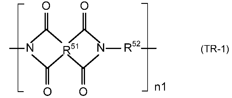
式(TR-1)中、R51は、環状構造、非環状構造、または環状構造と非環状構造を有する炭素数4~10の4価の基である。R52は、脂肪族炭化水素基、脂環族炭化水素基、芳香族炭化水素基、およびオルガノシロキサン基からなる群より選ばれる少なくとも1種の基を有する、炭素数2~39の2価の基であり、R52の主鎖には-O-、-SO2-、-CO-、-CH2-、-C(CH3)2-、-C2H4O-、および-S-からなる群から選ばれる少なくとも1種の基が介在していてもよい。n1は繰り返し単位であることを示す。n1は求められる物性に応じて適宜調整される。
式(TR-1)における好ましいR51としてはシクロヘキサン、シクロペンタン、シクロブタン、ビシクロペンタン、ビシクロオクタンおよびこれらの立体異性体から4個の水素原子を除いて形成される4価の基が挙げられる。より具体的には、下記構造式で表される4価の基が挙げられる。

第1の透明樹脂として使用可能な市販のポリイミド樹脂フィルムとして、ネオプリム(登録商標)L-3G30(三菱ガス化学(株)製、商品名)(このポリイミド樹脂フィルムには、シリカが含まれていてもよい)等が挙げられる。第1の透明樹脂はポリイミド樹脂のワニスから作製してもよく、使用可能なポリイミド樹脂ワニスとしてはネオプリム(登録商標)C-3G30(三菱ガス化学(株)製、商品名)があげられる。
第1の透明樹脂としてのポリカーボネート樹脂としては、例えば、日本国特開2001-296423号公報に記載された公知の透明性ポリカーボネート化合物のうち、上記第1の透明樹脂の要件を満足する透明樹脂が挙げられる。
上記第1の透明樹脂の要件を満足し得るポリカーボネート樹脂としては、例えば、ビスフェノール構造のジオール成分とカーボネート形成成分、例えば、ホスゲン類、ジフェニルカーボネート等のカーボネート類を用いて重合させて得られる一般的な透明性ポリカーボネート樹脂の構造が挙げられる。より具体的には、下記式(TR-2)で示されるポリカーボネート樹脂(TR-2)が挙げられる。式(TR-2)は、[]で囲まれる2つの単位の共重合体および/またはブレンド体を示す。
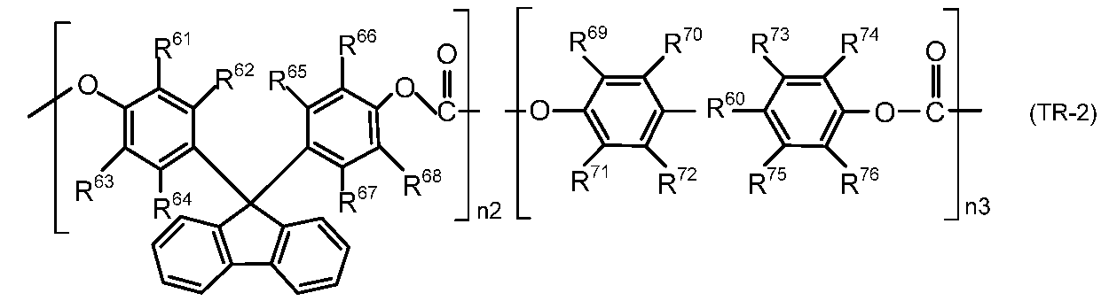
上記式(TR-2)において、R61~R68はそれぞれ独立に水素原子、ハロゲン原子または炭素数1~6の一価炭化水素基である。R69~R76はそれぞれ独立に水素原子、ハロゲン原子または炭素数1~22の一価炭化水素基である。R60は下記構造式で示される2価の基である。

Rはそれぞれ独立に水素原子、ハロゲン原子または炭素数1~22の一価炭化水素基であり、R’はそれぞれ独立に炭素数1~20の2価炭化水素基であり、Arは炭素数6~10のアリール基である。n2およびn3は共重合体および/またはブレンド体中の各単位のモル%である。n2は30~90モル%であり、n3は70~10モル%である。
第1の透明樹脂として使用可能な市販のポリカーボネート樹脂として、PURE-ACE(登録商標)M5(帝人(株)製、商品名)、同S5(帝人(株)製、商品名)等が挙げられる。
樹脂基材は、第1の透明樹脂を主成分とする。樹脂基材は、本発明の効果を損なわない範囲で、例えば、10質量%以下の範囲で、必要に応じて、任意成分を含有してもよい。任意成分としては、密着性付与剤、レベリング剤、帯電防止剤、熱安定剤、光安定剤、酸化防止剤、分散剤、難燃剤、滑剤、可塑剤等が挙げられる。
なお、第1の透明樹脂を主成分とする樹脂基材は、第1の透明樹脂と同様に、Tgが170℃以上であるのが好ましく、厚み100μmのときの波長350~1100nmの分光透過率曲線において、波長350~450nmの平均内部透過率が95%以上であり、波長400~450nmの最小内部透過率が97%以上であり、波長500nm以下の領域で内部透過率が90%となる波長が350nm以下であるのが好ましい。樹脂基材は、波長350~450nmの平均内部透過率および波長400~450nmの最小内部透過率が98%以上であり、波長500nm以下の領域で内部透過率が90%となる波長が340nm以下であるのがより好ましい。さらに、Tgおよび上記光学特性のより好ましい態様も第1の透明樹脂と同様にできる。
樹脂基材は、例えば、以下の方法で製造できる。樹脂基材は、第1の透明樹脂、または第1の透明樹脂と任意成分の混合物を溶融押出してフィルム状に成形して製造できる。また、第1の透明樹脂および必要に応じて任意成分を溶媒に溶解させ、塗工液を調製し、これを樹脂基材作製用の剥離性の基材に所望の厚さに塗工し乾燥させ、さらに、必要に応じて硬化させた後、樹脂基材を基材から剥離して、製造できる。
塗工液に用いる溶媒は、第1の透明樹脂を安定に分散できる分散媒または溶解できる溶媒であればよい。塗工液は、微小な泡によるボイド、異物等の付着による凹み、乾燥工程でのはじき等の改善のため界面活性剤を含んでもよい。さらに、塗工液の塗工には、例えば、浸漬コーティング法、キャストコーティング法、ダイコート法またはスピンコート法等を使用できる。
[吸収層]
吸収層は厚みが0.25μm以上12μm以下であり、NIR色素(A)と、Tgが170℃以上の第2の透明樹脂を含み、NIR色素(A)は、第2の透明樹脂との関係が(ii-1)および(ii-2)を満足する。NIR色素(A)は(i-1)および(i-2)を満足することが好ましい。吸収層は、典型的には、第2の透明樹脂中にNIR色素(A)が均一に溶解または分散した層である。
吸収層は厚みが0.25μm以上12μm以下であり、NIR色素(A)と、Tgが170℃以上の第2の透明樹脂を含み、NIR色素(A)は、第2の透明樹脂との関係が(ii-1)および(ii-2)を満足する。NIR色素(A)は(i-1)および(i-2)を満足することが好ましい。吸収層は、典型的には、第2の透明樹脂中にNIR色素(A)が均一に溶解または分散した層である。
吸収層の厚みは、0.25μm以上であれば、本フィルタにおける近赤外光の遮蔽性を十分とでき、12μm以下であれば本フィルタが高い可視光透過性を有する。吸収層の厚みは、0.4μm以上が好ましく、0.6μm以上がより好ましい。吸収層の厚みは、5μm以下が好ましく、2μm以下がより好ましい。なお、図2に示す光学フィルタ10Bのように吸収層を2層有する場合、吸収層の厚みは、合計で12μm以下が好ましく、5μm以下がより好ましく、3μm以下がさらに好ましい。この場合の各吸収層の厚みは、例えば、1.5μm以下が好ましく、1.4μm以下がより好ましい。
吸収層は、本発明の効果を損なわない範囲でNIR色素(A)以外にその他のNIR色素を含有してもよい。さらに、吸収層は、本発明の効果を損なわない範囲でNIR色素以外の色素、特にはUV色素を含有してもよい。
(NIR色素(A))
NIR色素(A)は、第2の透明樹脂との関係が上記(ii-1)および(ii-2)の要件を満足する。NIR色素(A)は、上記(i-1)および(i-2)の要件を満足することが好ましい。
NIR色素(A)は、第2の透明樹脂との関係が上記(ii-1)および(ii-2)の要件を満足する。NIR色素(A)は、上記(i-1)および(i-2)の要件を満足することが好ましい。
NIR色素(A)は、(ii-1)において、λmax(A)TRが680~745nmの波長領域にある。λmax(A)TRは690~730nmの波長領域にあるのがより好ましい。
NIR色素(A)は、(ii-2)において、T435-500ave(A)TRおよびT500-600ave(A)TRがともに94%以上である。T435-500ave(A)TRは、95%以上が好ましく、96%以上がより好ましい。T500-600ave(A)TRは、95%以上が好ましく、96%以上がより好ましい。
NIR色素(A)は、(i-1)において、λmax(A)DCMが670~735nmの波長領域にあるのが好ましい。λmax(A)DCMは680~720nmの波長領域にあるのがより好ましい。
NIR色素(A)は、(i-2)において、T435-500ave(A)DCMが94%以上であり、T500-600ave(A)DCMが94%以上であるのが好ましい。T435-500ave(A)DCMは、95%以上がより好ましく、96%以上がさらに好ましい。T500-600ave(A)DCMは、95%以上がより好ましく、96%以上がさらに好ましい。
第2の透明樹脂との関係において(ii-1)および(ii-2)の要件を満足し、好ましくは(i-1)および(i-2)の要件を満足する、NIR色素(A)を使用すれば、本フィルタにおいて、可視光の高い透過率と良好なNIR遮蔽特性の両方が達成できる。
NIR色素(A)は、第2の透明樹脂との関係が(ii-1)および(ii-2)の要件を満たし、好ましくは(i-1)および(i-2)の要件を満足する限り、分子構造は特に制限されない。具体的には、スクアリリウム色素が挙げられる。NIR色素(A)として、より具体的には、下記式(I)または式(II)で表されるスクアリリウム色素が好ましい。
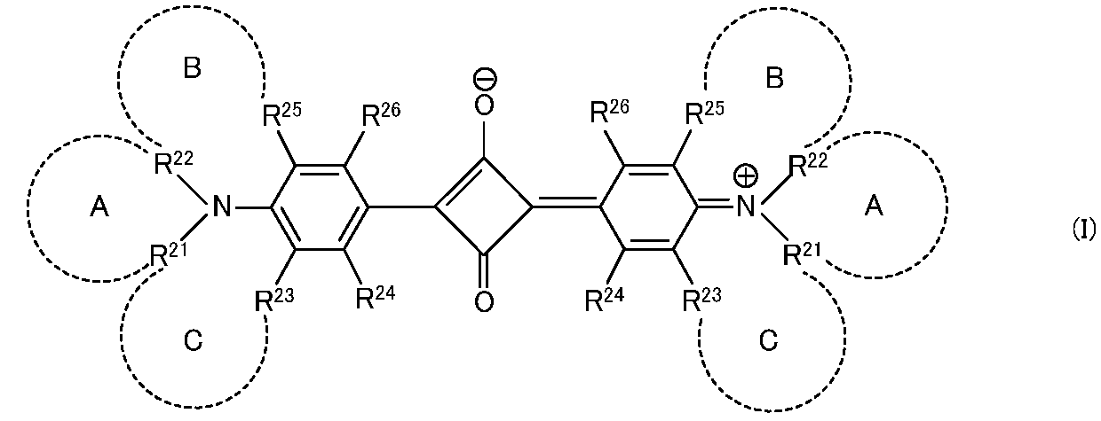
ただし、式(I)中の記号は以下のとおりである。
R24およびR26は、それぞれ独立して、水素原子、ハロゲン原子、水酸基、炭素数1~20のアルキル基もしくはアルコキシ基、炭素数1~10のアシルオキシ基、炭素数6~11のアリール基、置換基を有していてもよく炭素原子間に酸素原子を有していてもよい炭素数7~18のアルアリール基、-NR27R28(R27およびR28は、それぞれ独立して、水素原子、炭素数1~20のアルキル基、-C(=O)-R29(R29は、水素原子、ハロゲン原子、水酸基、置換基を有していてもよく、炭素原子間に不飽和結合、酸素原子、飽和もしくは不飽和の環構造を含んでよい炭素数1~25の炭化水素基)、-NHR30、または、-SO2-R30(R30は、それぞれ1つ以上の水素原子がハロゲン原子、水酸基、カルボキシ基、スルホ基、またはシアノ基で置換されていてもよく、炭素原子間に不飽和結合、酸素原子、飽和もしくは不飽和の環構造を含んでよい炭素数1~25の炭化水素基)を示す。)、または、下記式(S)で示される基(R41、R42は、独立して、水素原子、ハロゲン原子、または炭素数1~10のアルキル基もしくはアルコキシ基を示す。kは2または3である。)を示す。
R24およびR26は、それぞれ独立して、水素原子、ハロゲン原子、水酸基、炭素数1~20のアルキル基もしくはアルコキシ基、炭素数1~10のアシルオキシ基、炭素数6~11のアリール基、置換基を有していてもよく炭素原子間に酸素原子を有していてもよい炭素数7~18のアルアリール基、-NR27R28(R27およびR28は、それぞれ独立して、水素原子、炭素数1~20のアルキル基、-C(=O)-R29(R29は、水素原子、ハロゲン原子、水酸基、置換基を有していてもよく、炭素原子間に不飽和結合、酸素原子、飽和もしくは不飽和の環構造を含んでよい炭素数1~25の炭化水素基)、-NHR30、または、-SO2-R30(R30は、それぞれ1つ以上の水素原子がハロゲン原子、水酸基、カルボキシ基、スルホ基、またはシアノ基で置換されていてもよく、炭素原子間に不飽和結合、酸素原子、飽和もしくは不飽和の環構造を含んでよい炭素数1~25の炭化水素基)を示す。)、または、下記式(S)で示される基(R41、R42は、独立して、水素原子、ハロゲン原子、または炭素数1~10のアルキル基もしくはアルコキシ基を示す。kは2または3である。)を示す。
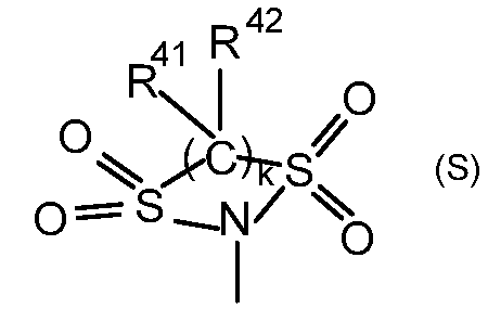
R21とR22、R22とR25、およびR21とR23は、互いに連結して窒素原子と共に員数が5または6のそれぞれ複素環A、複素環B、および複素環Cを形成してもよい。
複素環Aが形成される場合のR21とR22は、これらが結合した2価の基-Q-として、水素原子が炭素数1~6のアルキル基、炭素数6~10のアリール基または置換基を有していてもよい炭素数1~10のアシルオキシ基で置換されてもよいアルキレン基、またはアルキレンオキシ基を示す。
複素環Bが形成される場合のR22とR25、および複素環Cが形成される場合のR21とR23は、これらが結合したそれぞれ2価の基-X1-Y1-および-X2-Y2-(窒素に結合する側がX1およびX2)として、X1およびX2がそれぞれ下記式(1x)または(2x)で示される基であり、Y1およびY2がそれぞれ下記式(1y)~(5y)から選ばれるいずれかで示される基である。X1およびX2が、それぞれ下記式(2x)で示される基の場合、Y1およびY2はそれぞれ単結合であってもよく、その場合、炭素原子間に酸素原子を有してもよい。

式(1x)中、4個のZは、それぞれ独立して水素原子、水酸基、炭素数1~6のアルキル基もしくはアルコキシ基、または-NR38R39(R38およびR39は、それぞれ独立して、水素原子または炭素数1~20のアルキル基を示す)を示す。R31~R36はそれぞれ独立して水素原子、炭素数1~6のアルキル基または炭素数6~10のアリール基を、R37は炭素数1~6のアルキル基または炭素数6~10のアリール基を示す。
R27、R28、R29、R31~R37、複素環を形成していない場合のR21~R23、およびR25は、これらのうちの他のいずれかと互いに結合して5員環または6員環を形成してもよい。R31とR36、R31とR37は直接結合してもよい。
複素環を形成していない場合の、R21、R22、R23およびR25は、それぞれ独立して、水素原子、ハロゲン原子、水酸基、炭素数1~20のアルキル基もしくはアルコキシ基、炭素数1~10のアシルオキシ基、炭素数6~11のアリール基、または、置換基を有していてもよく炭素原子間に酸素原子を有していてもよい炭素数7~18のアルアリール基を示す。
なお、式(I)において、特に断りのない限り、炭化水素基はアルキル基、アリール基、またはアルアリール基である。特に断りのない限り、アルキル基および、アルコキシ基、アリール基またはアルアリール基におけるアルキル部分は、直鎖状、分岐鎖状、環状またはこれらの構造を組み合わせた構造でもよい。以下の他の式におけるアルキル基、アルコキシ基、アリール基、アルアリール基においても、同様である。式(I)において、R29における置換基としては、ハロゲン原子、水酸基、カルボキシ基、スルホ基、シアノ基、炭素数1~6のアシルオキシ基が挙げられる。R29を除いて「置換基を有してもよい」という場合の置換基としては、ハロゲン原子または炭素数1~15のアルコキシ基が例示できる。ハロゲン原子としては、フッ素原子、塩素原子、臭素原子、ヨウ素原子等が挙げられ、フッ素原子および塩素原子が好ましい。

ただし、式(II)中の記号は以下のとおりである。
環Zは、それぞれ独立して、ヘテロ原子を環中に0~3個有する5員環または6員環であり、環Zが有する水素原子は置換されていてもよい。水素原子が置換される場合、置換基としては、ハロゲン原子、または、置換基を有してもよい炭素数1~10のアルキル基が挙げられる。
環Zは、それぞれ独立して、ヘテロ原子を環中に0~3個有する5員環または6員環であり、環Zが有する水素原子は置換されていてもよい。水素原子が置換される場合、置換基としては、ハロゲン原子、または、置換基を有してもよい炭素数1~10のアルキル基が挙げられる。
R1とR2、R2とR3、およびR1と環Zを構成する炭素原子またはヘテロ原子は、互いに連結して窒素原子とともにそれぞれヘテロ環A1、ヘテロ環B1およびヘテロ環C1を形成していてもよく、その場合、ヘテロ環A1、ヘテロ環B1およびヘテロ環C1が有する水素原子は置換されていてもよい。水素原子が置換される場合、置換基としては、ハロゲン原子、または、置換基を有してもよい炭素数1~15のアルキル基が挙げられる。
ヘテロ環を形成していない場合のR1およびR2は、それぞれ独立して、水素原子、ハロゲン原子、または、炭素原子間に不飽和結合、ヘテロ原子、飽和もしくは不飽和の環構造を含んでよく、置換基を有してもよい炭化水素基を示す。R4およびヘテロ環を形成していない場合のR3は、それぞれ独立して、水素原子、ハロゲン原子、または炭素原子間にヘテロ原子を含んでもよく、置換基を有してもよいアルキル基もしくはアルコキシ基を示す。
ヘテロ環を形成していない場合のR1およびR2は、それぞれ独立して、水素原子、ハロゲン原子、または、炭素原子間に不飽和結合、ヘテロ原子、飽和もしくは不飽和の環構造を含んでよく、置換基を有してもよい炭化水素基を示す。R4およびヘテロ環を形成していない場合のR3は、それぞれ独立して、水素原子、ハロゲン原子、または炭素原子間にヘテロ原子を含んでもよく、置換基を有してもよいアルキル基もしくはアルコキシ基を示す。
式(II)において、炭化水素基の炭素数は1~15が挙げられる。アルキル基もしくはアルコキシ基の炭素数は1~10が挙げられる。式(II)において、「置換基を有してもよい」という場合の置換基としては、ハロゲン原子または炭素数1~10のアルコキシ基が例示できる。ハロゲン原子としては、フッ素原子、塩素原子、臭素原子、ヨウ素原子等が挙げられ、フッ素原子および塩素原子が好ましい。
化合物(I)としては、例えば、式(I-1)~(I-4)のいずれかで示される化合物が挙げられる。
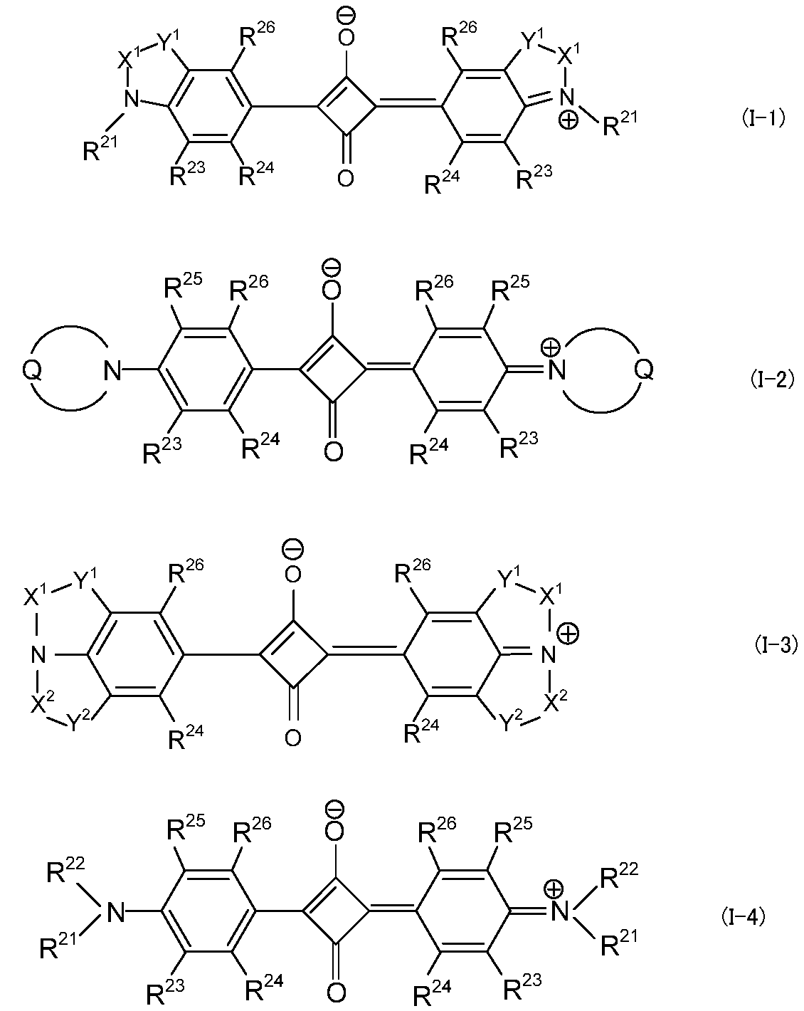
ただし、式(I-1)~式(I-4)中の記号は、式(I)における同記号の各規定と同じであり、好ましい態様も同様である。
化合物(I-1)~(I-4)のうちでも、NIR色素(A)としては、吸収層の可視光透過率を高くできる観点から化合物(I-1)~(I-3)が好ましく、化合物(I-1)が特に好ましい。
化合物(I-1)において、X1としては、基(2x)が好ましく、Y1としては、単結合または基(1y)が好ましい。この場合、R31~R36としては、水素原子または炭素数1~3のアルキル基が好ましく、水素原子またはメチル基がより好ましい。なお、-Y1-X1-として、具体的には、式(11-1)~(12-3)で示される2価の有機基が挙げられる。
-C(CH3)2-CH(CH3)- …(11-1)
-C(CH3)2-CH2- …(11-2)
-C(CH3)2-CH(C2H5)- …(11-3)
-C(CH3)2-C(CH3)(nC3H7)- …(11-4)
-C(CH3)2-CH2-CH2- …(12-1)
-C(CH3)2-CH2-CH(CH3)- …(12-2)
-C(CH3)2-CH(CH3)-CH2- …(12-3)
-C(CH3)2-CH2- …(11-2)
-C(CH3)2-CH(C2H5)- …(11-3)
-C(CH3)2-C(CH3)(nC3H7)- …(11-4)
-C(CH3)2-CH2-CH2- …(12-1)
-C(CH3)2-CH2-CH(CH3)- …(12-2)
-C(CH3)2-CH(CH3)-CH2- …(12-3)
また、化合物(I-1)において、R21は、溶解性、耐熱性、さらに分光透過率曲線における可視域と近赤外域の境界付近の変化の急峻性の観点から、独立して、式(4-1)または式(4-2)で示される基がより好ましい。

式(4-1)および式(4-2)中、R81~R85は、独立して、水素原子、ハロゲン原子、または炭素数1~4のアルキル基を示す。
化合物(I-1)において、R24は-NR27R28が好ましい。-NR27R28としては、第2の透明樹脂や樹脂基材上に吸収層を形成する際に用いる溶媒(以下、「ホスト溶媒」ともいう)への溶解性の観点から、-NH-C(=O)-R29が好ましい。化合物(I-1)において、R24が-NH-C(=O)-R29の化合物を式(I-11)に示す。

化合物(I-11)における、R23およびR26は、独立して、水素原子、ハロゲン原子、または炭素数1~6のアルキル基もしくはアルコキシ基が好ましく、いずれも水素原子がより好ましい。
化合物(I-11)において、R29としては、置換基を有していてもよい炭素数1~20のアルキル基、置換基を有していてもよい炭素数6~10のアリール基、または置換基を有していてもよく、炭素原子間に酸素原子を有していてもよい炭素数7~18のアルアリール基が好ましい。置換基としては、フッ素原子等のハロゲン原子、水酸基、カルボキシ基、スルホ基、シアノ基、炭素数1~6のアルキル基、炭素数1~6のフロロアルキル基、炭素数1~6のアルコキシ基、炭素数1~6のアシルオキシ基等が挙げられる。
R29としては、水素原子、ハロゲン原子、水酸基、炭素数1~20のアルキル基もしくはアルコキシ基、炭素数1~10のアシルオキシ基、炭素数6~11のアリール基、または、置換基を有していてもよく炭素原子間に酸素原子を有していてもよい炭素数7~18のアルアリール基が好ましい。
R29としては、フッ素原子で置換されてもよい直鎖状、分岐鎖状、環状の炭素数1~17のアルキル基、炭素数1~6のフロロアルキル基および/または炭素数1~6のアルコキシ基で置換されてもよいフェニル基、および炭素原子間に酸素原子を有していてもよい炭素数7~18の、末端に炭素数1~6のフッ素原子で置換されていてもよいアルキル基および/または、炭素数1~6のアルコキシ基で置換されてもよいフェニル基を有するアルアリール基から選ばれる基が好ましい。
R29としては、独立して1つ以上の水素原子がハロゲン原子、水酸基、カルボキシ基、スルホ基、またはシアノ基で置換されていてもよく、炭素原子間に不飽和結合、酸素原子、飽和もしくは不飽和の環構造を含んでよい、少なくとも1以上の分岐を有する炭素数5~25の炭化水素基である基も好ましく使用できる。このようなR29としては、例えば、下記式(1a)、(1b)、(2a)~(2e)、(3a)~(3e)で示される基が挙げられる。
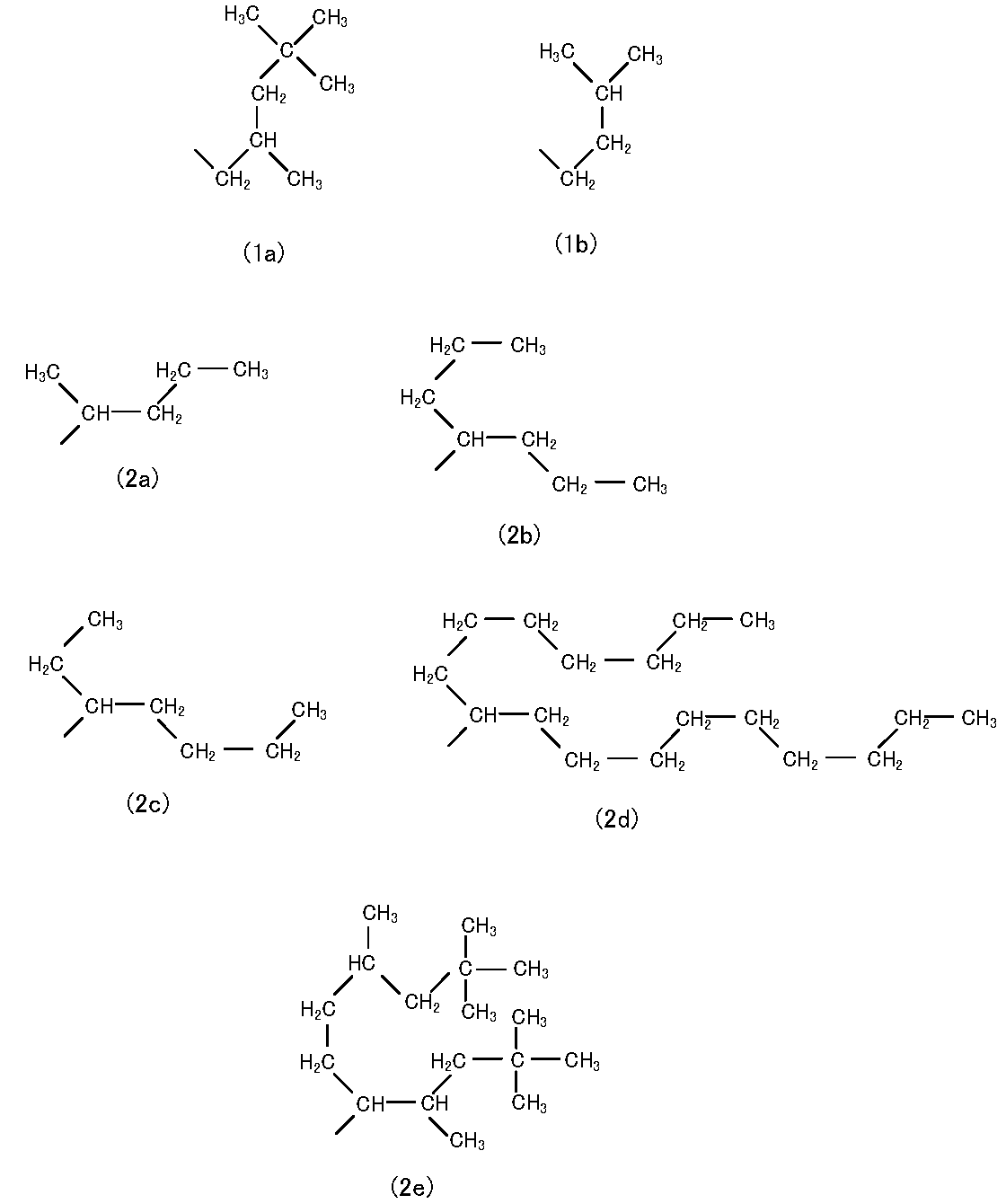

化合物(I-11)としては、より具体的に、以下の表1に示す化合物が挙げられる。なお、表1において、基(11-1)を(11-1)と示す。他の基についても同様である。以下の他の表においても基の表示は同様である。また、表1に示す化合物は、いずれもスクアリリウム骨格の左右において各記号の意味は同一である。以下の他の表に示すスクアリリウム色素においても同様である。

化合物(I-1)において、R24は、可視光の透過率、特に波長430~550nmの光の透過率を高める観点から、-NH-SO2-R30が好ましい。化合物(I-1)において、R24が-NH-SO2-R30の化合物を式(I-12)に示す。

化合物(I-12)における、R23およびR26は、独立して、水素原子、ハロゲン原子、または炭素数1~6のアルキル基もしくはアルコキシ基が好ましく、いずれも水素原子がより好ましい。
化合物(I-12)において、R30は耐光性の点から、独立して、分岐を有してもよい炭素数1~12のアルキル基もしくはアルコキシ基、または不飽和の環構造を有する炭素数6~16の炭化水素基が好ましい。不飽和の環構造としては、ベンゼン、トルエン、キシレン、フラン、ベンゾフラン等が挙げられる。R30は、独立して、分岐を有してもよい炭素数1~12のアルキル基もしくはアルコキシ基がより好ましい。なお、R30を示す各基において、水素原子の一部または全部がハロゲン原子、特にはフッ素原子に置換されていてもよい。なお、水素原子のフッ素原子へ置換は、色素(I-12)を含有する吸収層と樹脂基材との密着性が落ちない程度とする。
不飽和の環構造を有するR30として具体的には、下記式(P1)~(P8)で示される基が挙げられる。

化合物(I-12)としては、より具体的に、以下の表2に示す化合物が挙げられる。

化合物(II)としては、例えば、式(II-1)~(II-3)のいずれかで示される化合物が挙げられる。

ただし、式(II-1)、式(II-2)中、R1およびR2は、それぞれ独立に水素原子、ハロゲン原子、または、置換基を有してもよい炭素数1~15のアルキル基を示し、R3~R6はそれぞれ独立に水素原子、ハロゲン原子、または、置換基を有してもよい炭素数1~10のアルキル基を示す。
ただし、式(II-3)中、R1、R4、およびR9~R12は、それぞれ独立に水素原子、ハロゲン原子、または、置換基を有してもよい炭素数1~15のアルキル基を示し、R7およびR8はそれぞれ独立に水素原子、ハロゲン原子、または、置換基を有してもよい炭素数1~5のアルキル基を示す。
化合物(II-1)および化合物(II-2)におけるR1およびR2は、透明樹脂への溶解性、可視光透過性等の観点から、独立して、炭素数1~15のアルキル基が好ましく、炭素数7~15のアルキル基がより好ましく、R1とR2の少なくとも一方が、炭素数7~15の分岐鎖を有するアルキル基がさらに好ましく、R1とR2の両方が炭素数8~15の分岐鎖を有するアルキル基が特に好ましい。
R3は、透明樹脂への溶解性、可視光透過性等の観点から、独立して、水素原子、ハロゲン原子、炭素数1~3のアルキル基が好ましく、水素原子、ハロゲン原子、メチル基がより好ましい。R4は、可視域と近赤外域の境界付近の変化の急峻性の観点から、水素原子、ハロゲン原子が好ましく、水素原子がとくに好ましい。化合物(II-1)におけるR5および化合物(II-2)におけるR6は、独立して、水素原子、ハロゲン原子、ハロゲン原子で置換されていてもよい炭素数1~5のアルキル基が好ましく、水素原子、ハロゲン原子、メチル基がより好ましい。
化合物(II-1)および化合物(II-2)としては、より具体的に、それぞれ以下の表3および表4に示す化合物が挙げられる。表3および表4において、-C8H17、-C4H9、-C6H13は、直鎖のオクチル基、ブチル基、ヘキシル基をそれぞれ示す。


化合物(II-3)におけるR1は、透明樹脂への溶解性、可視光透過性等の観点から、独立して、炭素数1~15のアルキル基が好ましく、炭素数1~10のアルキル基がより好ましく、エチル基、イソプロピル基が特に好ましい。
R4は、可視光透過性、合成容易性の観点から、水素原子、ハロゲン原子が好ましく、水素原子が特に好ましい。R7およびR8は、独立して、水素原子、ハロゲン原子、ハロゲン原子で置換されていてもよい炭素数1~5のアルキル基が好ましく、水素原子、ハロゲン原子、メチル基がより好ましい。
R9~R12は、独立して、水素原子、ハロゲン原子、ハロゲン原子で置換されていてもよい炭素数1~5のアルキル基が好ましい。-CR9R10-CR11R12-として、上記基(11-1)~(11-3)または、以下の式(11-5)で示される2価の有機基が挙げられる。
-C(CH3)(CH2-CH(CH3)2)-CH(CH3)-…(11-5)
-C(CH3)(CH2-CH(CH3)2)-CH(CH3)-…(11-5)
化合物(II-3)としては、より具体的に、以下の表5に示す化合物が挙げられる。

NIR色素(A)としては、これらの中でも、第2の透明樹脂やホスト溶媒への溶解性、可視透過性の点から、色素(I-11)および色素(I-12)が好ましく、表1に示す色素(I-11)および表2に示す色素(I-12)がより好ましい。さらに、これらの中でも、色素(I-11-7)、色素(I-11-20)、色素(I-12-2)、色素(I-12-9)、色素(I-12-15)、色素(I-12-25)等が好ましい。
NIR色素(A)は、1種の化合物からなってもよく、2種以上の化合物からなってもよい。2種以上の化合物からなる場合は、個々の化合物がNIR色素(A)の性質を必ずしも有する必要はなく、混合物として、NIR色素(A)の性質を有すればよい。
化合物(I)および化合物(II)は、それぞれ公知の方法で、製造できる。化合物(I)について、化合物(I-11)は、例えば、米国特許第5,543,086号明細書に記載された方法で製造できる。化合物(I-12)は、例えば、米国特許出願公開第2014/0061505号明細書、国際公開第2014/088063号明細書に記載された方法で製造可能である。化合物(II)については、国際公開第2017/135359号明細書に記載された方法で製造可能である。
吸収層におけるNIR色素(A)の含有量は、吸収層の厚みによるが、NIR遮蔽性および溶解性の観点から、第2の透明樹脂に100質量部に対して、0.1~20質量部が好ましく、1~20質量部がより好ましい。吸収層の厚みが5μm以下の場合には、吸収層におけるNIR色素(A)の含有量は、第2の透明樹脂に100質量部に対して、5~20質量部が好ましく、5~15質量部がより好ましい。
吸収層はNIR色素(A)に加えて、本発明の効果を損なわない範囲でその他のNIR色素を含有してもよい。その他のNIR色素としては、ジクロロメタンに溶解して測定される波長350~1100nmの分光透過率曲線において、最大吸収波長が735nm超1200nm以下の波長領域にあるNIR色素が挙げられる。
その他のNIR色素としては、例えば、上記最大吸収波長を有する、シアニン色素、フタロシアニン色素、ナフタロシアニン色素、ジチオール金属錯体色素、ジイモニウム色素、ポリメチン色素、フタリド色素、ナフトキノン色素、アントラキノン色素、インドフェノール色素、スクアリリウム色素からなる群から選ばれる少なくとも1種の色素が挙げられる。
最大吸収波長が735nm超1200nm以下の波長領域にあるNIR色素としては、例えば、下記式(2)で示されるスクアリリウム色素が好ましい。
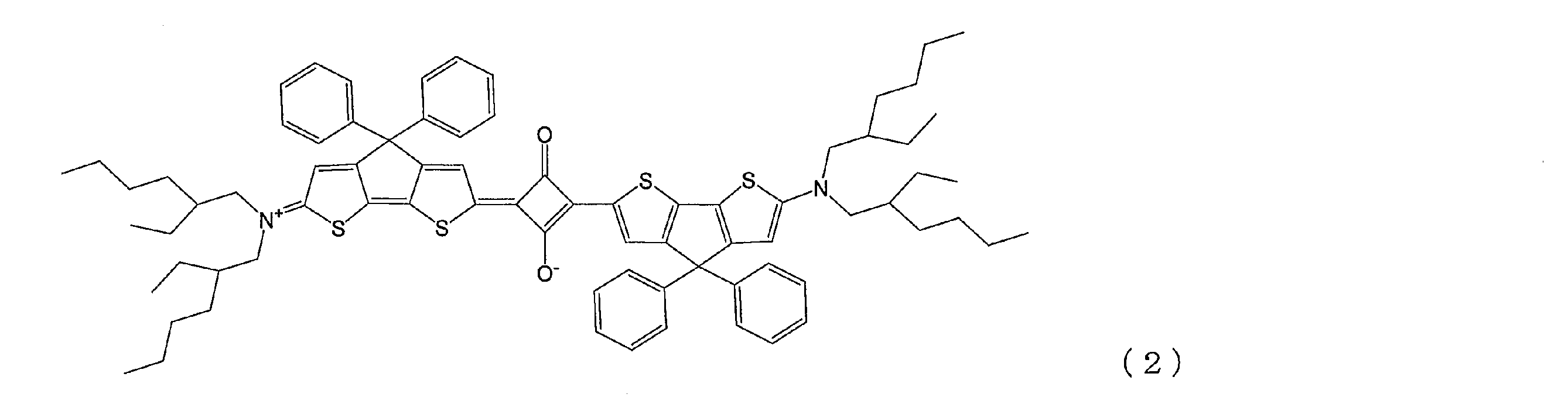
その他のNIR色素を用いる場合の吸収層におけるその他のNIR色素の含有量は、第2の透明樹脂に100質量部に対して、0.1~18質量部が挙げられる。ただし、吸収層における色素全体の含有量が、第2の透明樹脂に100質量部に対して、20質量部以下となることが好ましい。
(UV色素)
吸収層が任意に含有するUV色素としては、下記(iii-1)の要件を満足するUV色素(U)が好ましい。
吸収層が任意に含有するUV色素としては、下記(iii-1)の要件を満足するUV色素(U)が好ましい。
(iii-1)UV色素(U)をジクロロメタンに溶解して測定される波長350~1100nmの分光透過率曲線において、最大吸収波長λmax(U)DCMが380~420nmの波長領域にある。UV色素(U)の最大吸収波長λmax(U)DCMは、波長380~415nmにあるとより好ましく、波長390~410nmにあるとさらに好ましい。
UV色素(U)の具体例としては、オキサゾール色素、メロシアニン色素、シアニン色素、ナフタルイミド色素、オキサジアゾール色素、オキサジン色素、オキサゾリジン色素、ナフタル酸色素、スチリル色素、アントラセン色素、環状カルボニル色素、トリアゾール色素等が挙げられる。この中でも、オキサゾール色素、メロシアニン色素が好ましく、メロシアニン色素がより好ましい。UV色素(U)は、吸収層に1種を単独で用いてもよく、2種以上を併用してもよい。
UV色素(U)は、さらに、下記(iii-2)の要件を満足することが好ましい。
(iii-2)UV色素(U)をジクロロメタンに最大吸収波長λmax(u)DCMにおける透過率が1%となるように含有させて測定される、波長350~1100nmの分光透過率曲線において、波長435~500nmの平均透過率(以下、「T435-500ave(u)DCM」で示す。)が94%以上であり、かつ、波長500~600nmの平均透過率(以下、「T500-600ave(u)DCM」で示す。)が94%以上である。
(iii-2)UV色素(U)をジクロロメタンに最大吸収波長λmax(u)DCMにおける透過率が1%となるように含有させて測定される、波長350~1100nmの分光透過率曲線において、波長435~500nmの平均透過率(以下、「T435-500ave(u)DCM」で示す。)が94%以上であり、かつ、波長500~600nmの平均透過率(以下、「T500-600ave(u)DCM」で示す。)が94%以上である。
T435-500ave(u)DCMは、95%以上が好ましく、96%以上がより好ましい。T500-600ave(u)DCMは、95%以上が好ましく、96%以上がより好ましい。
NIR色素(A)とともに、(iii-1)に加えて(iii-2)を満足するUV色素(U)を使用すれば、本フィルタにおいて、可視光の高い透過率と良好なNIR遮蔽特性およびUV遮蔽特性を達成できる。
UV色素(U)としては、特に、式(M)で示されるメロシアニン色素が好ましい。
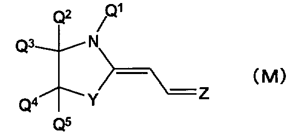
式(M)中、Yは、置換もしくは非置換のメチレン基または酸素原子を示す。置換されたメチレン基の置換基としては、ハロゲン原子、および炭素数1~10のアルキル基またはアルコキシ基が挙げられ、好ましくは炭素数1~10のアルキル基またはアルコキシ基である。Yが置換もしくは非置換のメチレン基の場合、非置換のメチレン基または水素原子の1つが炭素数1~4のアルキル基で置換されたメチレン基が好ましく、非置換のメチレン基が特に好ましい。
Q1は、置換または非置換の炭素数1~12の1価の炭化水素基を表す。Q1が、置換された炭化水素基であるの場合の置換基としては、アルコキシ基、アシル基、アシルオキシ基、シアノ基、ジアルキルアミノ基または塩素原子が好ましい。上記アルコキシ基、アシル基、アシルオキシ基およびジアルキルアミノ基の炭素数は1~6が好ましい。
上記の置換基を有しないQ1として具体的には、水素原子の一部が脂肪族環、芳香族環もしくはアルケニル基で置換されていてもよい炭素数1~12のアルキル基、水素原子の一部が芳香族環、アルキル基もしくはアルケニル基で置換されていてもよい炭素数3~8のシクロアルキル基、および水素原子の一部が脂肪族環、アルキル基もしくはアルケニル基で置換されていてもよい炭素数6~12のアリール基が好ましい。
Q1が非置換のアルキル基である場合、そのアルキル基は直鎖状であっても、分岐状であってもよく、その炭素数は1~6がより好ましい。
Q1が、水素原子の一部が脂肪族環、芳香族環もしくはアルケニル基で置換された炭素数1~12のアルキル基である場合、炭素数3~6のシクロアルキル基を有する炭素数1~4のアルキル基、フェニル基で置換された炭素数1~4のアルキル基がより好ましく、フェニル基で置換された炭素数1または2のアルキル基が特に好ましい。なお、アルケニル基で置換されたアルキル基とは、全体としてアルケニル基であるが1、2位間に不飽和結合を有しないものを意味し、例えばアリル基や3-ブテニル基等をいう。
好ましいQ1は、水素原子の一部がシクロアルキル基またはフェニル基で置換されていてもよい炭素数1~6のアルキル基である。特に好ましいQ1は炭素数1~6のアルキル基であり、具体的には、メチル基、エチル基、n-プロピル基、イソプロピル基、n-ブチル基、イソブチル基、t-ブチル基等が挙げられる。
Q2~Q5は、それぞれ独立に、水素原子、ハロゲン原子、または、炭素数1~10のアルキル基もしくはアルコキシ基を表す。アルキル基およびアルコキシ基の炭素数は1~6が好ましく、1~4がより好ましい。
Q2およびQ3は、少なくとも一方が、アルキル基が好ましく、いずれもアルキル基がより好ましい。Q2またはQ3がアルキル基でない場合は、水素原子がより好ましい。Q2およびQ3は、いずれも炭素数1~6のアルキル基が特に好ましい。
Q4およびQ5は、少なくとも一方が、水素原子が好ましく、いずれも水素原子がより好ましい。Q4またはQ5が水素原子でない場合は、炭素数1~6のアルキル基が好ましい。
Zは、式(Z1)~(Z5)で表される2価の基のいずれかを表す。
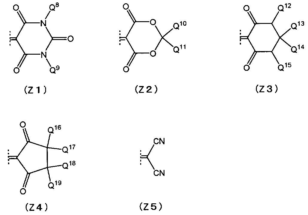
式(Z1)~(Z5)において、Q8~Q19は、それぞれ独立に置換または非置換の炭素数1~12の1価の炭化水素基を表す。これらが、置換された炭化水素基であるの場合の置換基としては、Q1における置換基と同様の置換基が挙げられ、好ましい態様も同様である。Q8~Q19が置換基を有しない炭化水素基である場合、置換基を有しないQ1と同様の態様が挙げられる。
式(Z1)において、Q8およびQ9は異なる基であってもよいが、同一の基が好ましい。Q8およびQ9が非置換のアルキル基である場合、そのアルキル基は直鎖状であっても、分岐状であってもよく、その炭素数は1~6がより好ましい。
好ましいQ8およびQ9は、いずれも、水素原子の一部がシクロアルキル基またはフェニル基で置換されていてもよい炭素数1~6のアルキル基である。特に好ましいQ8およびQ9は、いずれも、炭素数1~6のアルキル基であり、具体的には、例えば、メチル基、エチル基、n-プロピル基、イソプロピル基、n-ブチル基、イソブチル基、t-ブチル基等が挙げられる。
式(Z2)において、Q10とQ11は、いずれも、炭素数1~6のアルキル基がより好ましく、それらは同一のアルキル基が特に好ましい。
式(Z3)において、Q12およびQ15は、いずれも水素原子であるか、置換基を有しない炭素数1~6のアルキル基が好ましい。同じ炭素原子に結合した2つの基であるQ13とQ14は、いずれも水素原子であるか、いずれも炭素数1~6のアルキル基が好ましい。式(Z4)における、同じ炭素原子に結合した2つの基Q16とQ17およびQ18とQ19は、いずれも水素原子であるか、いずれも炭素数1~6のアルキル基が好ましい。
式(M)で表される化合物としては、Yが酸素原子であり、Zが基(Z1)または基(Z2)である化合物、および、Yが非置換のメチレン基であり、Zが基(Z1)または基(Z5)である化合物が好ましい。
色素(M)の具体例としては、より具体的に、以下の表6に示す化合物が挙げられる。なお、表6において-C3H7はn-プロピル基を示す。
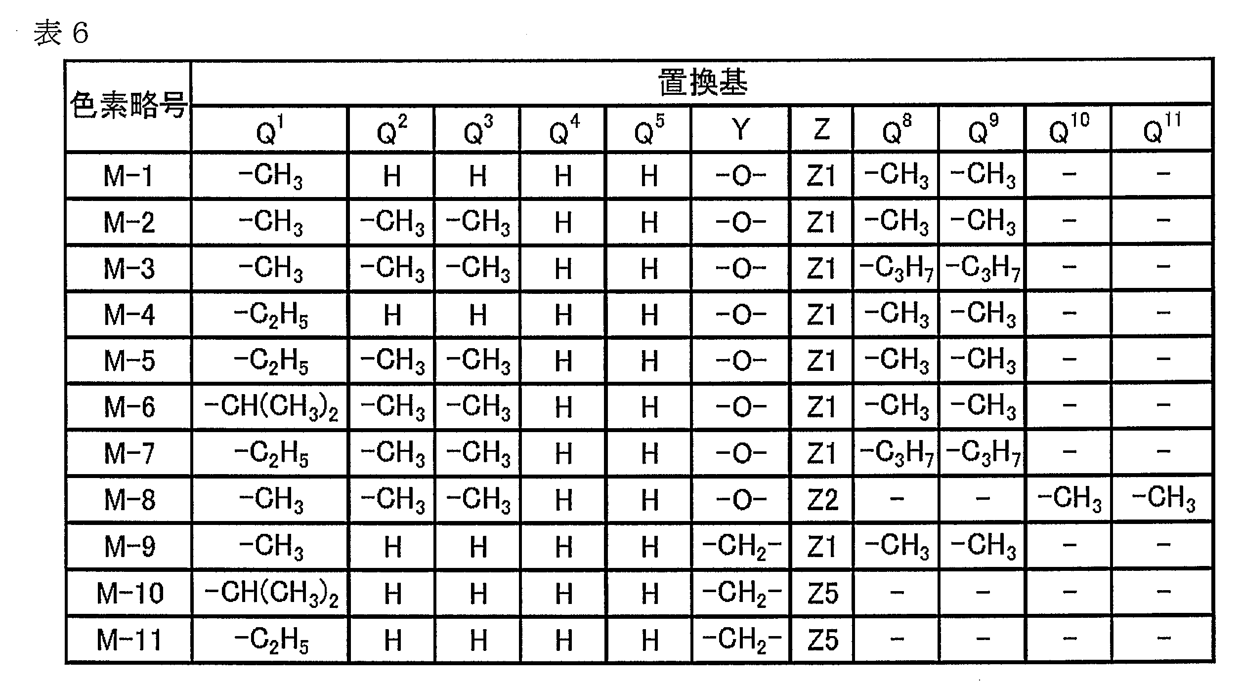
UV色素(U)としては、これらの中でも、第2の透明樹脂や、ホスト溶媒への溶解性、可視透過性、特には(iii-2)を満足できる等の点から、色素(M-1)、色素(M-2)、色素(M-5)、色素(M-6)等が好ましい。なお、化合物(M)は公知の方法で製造できる。
UV色素(U)は、1種の化合物からなってもよく、2種以上の化合物からなってもよい。2種以上の化合物からなる場合は、個々の化合物がUV色素(U)の性質を必ずしも有する必要はなく、混合物として、UV色素(U)の性質を有すればよい。
吸収層におけるUV色素(U)の含有量は、吸収層の厚みによるが、UV遮蔽性および溶解性の観点から、第2の透明樹脂に100質量部に対して、0.01~~20質量部が好ましく、0.05~20質量部がより好ましく、0.1~20質量部がさらに好ましい。なお、吸収層はUV色素(U)に加えて、本発明の効果を損なわない範囲でその他のUV色素を含有してもよい。
(第2の透明樹脂)
第2の透明樹脂は、Tgが170℃以上の樹脂である。第2の透明樹脂のTgは170℃以上であれば、吸収層は、高温使用においてNIR色素(A)の光学特性を維持する耐熱性に優れる。さらに、好ましい態様において、熱や応力による変形が生じにくく、本フィルタにおいて誘電体多層膜の密着性に優れる。Tgは、200℃以上が好ましく、250℃以上がより好ましい。Tgの上限は特にないが、成形加工性等の観点から、第2の透明樹脂のTgは400℃以下が好ましい。
第2の透明樹脂は、Tgが170℃以上の樹脂である。第2の透明樹脂のTgは170℃以上であれば、吸収層は、高温使用においてNIR色素(A)の光学特性を維持する耐熱性に優れる。さらに、好ましい態様において、熱や応力による変形が生じにくく、本フィルタにおいて誘電体多層膜の密着性に優れる。Tgは、200℃以上が好ましく、250℃以上がより好ましい。Tgの上限は特にないが、成形加工性等の観点から、第2の透明樹脂のTgは400℃以下が好ましい。
さらに、第2の透明樹脂は、NIR色素(A)との関係において、上記(ii-1)および(ii-2)の要件を満足する。(ii-1)および(ii-2)の要件における好ましい範囲は、NIR色素(A)において説明したとおりである。
第2の透明樹脂は、Tgが170℃以上であり、NIR色素(A)との関係において、上記(ii-1)および(ii-2)の要件を満足すれば、種類は特に制限されず、例えば、アクリル樹脂、エポキシ樹脂、エン・チオール樹脂、ポリカーボネート樹脂、ポリエーテル樹脂、ポリアリレート樹脂、ポリサルホン樹脂、ポリエーテルサルホン樹脂、ポリパラフェニレン樹脂、ポリアリーレンエーテルフォスフィンオキシド樹脂、ポリイミド樹脂、ポリアミドイミド樹脂、ポリオレフィン樹脂、ポリシクロオレフィン樹脂、およびポリエステル樹脂等から選ばれる1種以上が使用される。
第2の透明樹脂としては、第1の透明樹脂として例示したのと同様の樹脂が使用可能である。なお、吸収層の厚みが樹脂基材の厚みに比べて小さいことから、第1の透明樹脂と比べて可視光透過性において必ずしも高いレベルを要求されない。ただし、第2の透明樹脂は、NIR色素(A)との関係において(ii-1)および(ii-2)の要件を満足する可視光透明性が要求される。
さらに、誘電体多層膜との密着性の観点から、第2の透明樹脂としては、ポリイミド樹脂が好ましく、特には、ポリイミド樹脂(TR-1)が好ましい。
第2の透明樹脂として使用可能な市販のポリカーボネート樹脂として、FPC-0220(三菱ガス化学(株)社製、商品名)、PURE-ACE(登録商標)M5(帝人(株)製、商品名)、同S5(帝人(株)製、商品名)等が挙げられる。
第2の透明樹脂として使用可能な市販のポリイミド樹脂として、ワニスの形態で得られる、ネオプリム(登録商標)C-3650(三菱ガス化学(株)製、商品名)、同C-3G30(三菱ガス化学(株)製、商品名)、同C-3450(三菱ガス化学(株)製、商品名)、同P500(三菱ガス化学(株)製、商品名)、JL-20(新日本理化製、商品名)(これらのポリイミド樹脂のワニスには、シリカが含まれていてもよい)等が挙げられる。
吸収層は、可視光の高い透過性を維持する観点から、上記したNIR色素(A)、UV色素(U)、その他のNIR色素、その他のUV色素等の色素と第2の透明樹脂のみで構成されるのが好ましい。各色素の含有量および色素の合計の含有量は上記したとおりである。
ただし、吸収層は、本発明の効果を損なわない範囲で、密着性付与剤、色調補正色素、レベリング剤、帯電防止剤、熱安定剤、光安定剤、酸化防止剤、分散剤、難燃剤、滑剤、可塑剤等の任意成分を有してもよい。
吸収層は、例えば、NIR色素(A)と、第2の透明樹脂または第2の透明樹脂の原料成分と、必要に応じて配合されるNIR色素(A)以外の色素や各種成分、例えばUV色素(U)とを、溶媒に溶解または分散させて塗工液を調製し、これを基材に塗工し乾燥させ、さらに必要に応じて硬化させて形成できる。上記基材は、本フィルタに含まれる樹脂基材でもよいし、吸収層を形成する際にのみ使用する剥離性の基材でもよい。また、溶媒は、安定に分散できる分散媒または溶解できる溶媒であればよい。例えば、700nm帯域以上の波長で効果的に吸収を増やしたい場合、その他のNIR色素として上述した、最大吸収波長が735nm超1200nm以下の波長領域にあるNIR色素を添加してもよい。
また、塗工液は、微小な泡によるボイド、異物等の付着による凹み、乾燥工程でのはじき等の改善のため界面活性剤を含んでもよい。さらに、塗工液の塗工には、例えば、浸漬コーティング法、キャストコーティング法、ダイコート法またはスピンコート法等を使用できる。上記塗工液を基材上に塗工後、乾燥させることにより吸収層が形成される。また、塗工液が第2の透明樹脂の原料成分を含有する場合、さらに熱硬化、光硬化等の硬化処理を行う。
また、吸収層は、押出成形によりフィルム状に製造可能でもあり、このフィルムを他の部材、例えば、樹脂基材に積層し熱圧着等により一体化させてもよい。
上記所定の厚みを有し、NIR色素(A)および第2の透明樹脂を含有する吸収層を吸収層(X)とすると、吸収層(X)は、図1の光学フィルタ10Aのように樹脂基材1の一方の主面上に1層有してもよく、図2の光学フィルタ10Bのように樹脂基材1の両主面上に各1層ずつ合計2層有してもよい。吸収層(X)を2層有する場合、各吸収層(X)は同じ構成であっても異なってもよい。
光学フィルタ10Bに示す、第1の吸収層2aおよび第2の吸収層2bは、一方が吸収層(X)であって、他方がその他の吸収層であってもよい。例えば、第1の吸収層2aを、NIR色素(A)および第2の透明樹脂を含有する吸収層(X)とし、第2の吸収層2bをUV色素(U)および第2の透明樹脂を含有するその他の吸収層としてもよい。
光学フィルタ10Bにおける、第1の吸収層2aおよび第2の吸収層2bは、いずれも、NIR色素(A)および第2の透明樹脂を含有し、任意にUV色素(U)を含有する吸収層(X)で構成され、厚みがそれぞれ5μm以下であるのが好ましい。この場合、第1の吸収層2aおよび第2の吸収層2bにおける第2の透明樹脂は、ポリイミド樹脂が好ましく、2つの吸収層の厚みはいずれも1.5μm以下であるのが特に好ましい。
本フィルタは、吸収層が樹脂基材の少なくとも一方の主面上に配置された吸収層付き樹脂基材、すなわち本フィルタから誘電体多層膜を除いた状態、で測定される波長350~1100nmの分光透過率曲線において、以下の(v-1)~(v-4)の特性を満足することが好ましい。これにより、本フィルタは、可視光の高い透過性および近赤外光の高い遮蔽性を有する。
具体的には、図1に示す光学フィルタ10Aであれば、樹脂基材1の一方の主面に吸収層2が積層された構成、図2に示す光学フィルタ10Bであれば、樹脂基材1の両方の主面に第1の吸収層2aおよび第2の吸収層2bがそれぞれ積層された構成において測定される波長350~1100nmの分光透過率曲線が、以下の(v-1)~(v-4)の特性を満足することが好ましい。なお、これらの光学特性は入射角0度における光学特性である。
(v-1)光学フィルタの波長435~480nmの平均内部透過率が90.5%以上である。該平均内部透過率は、より好ましくは91%以上、さらに好ましくは91.5%以上である。
(v-2)光学フィルタの波長500~600nmの平均内部透過率が90.5%以上である。該平均内部透過率は、より好ましくは92%以上、さらに好ましくは93%以上である。
(v-3)光学フィルタの波長600~740nmで内部透過率が20%となる波長が650~685nmの波長領域にある。
(v-4)光学フィルタの波長700~730nmの平均内部透過率が3%以下である。該平均内部透過率は、より好ましくは2%以下、さらに好ましくは1%以下である。
(v-2)光学フィルタの波長500~600nmの平均内部透過率が90.5%以上である。該平均内部透過率は、より好ましくは92%以上、さらに好ましくは93%以上である。
(v-3)光学フィルタの波長600~740nmで内部透過率が20%となる波長が650~685nmの波長領域にある。
(v-4)光学フィルタの波長700~730nmの平均内部透過率が3%以下である。該平均内部透過率は、より好ましくは2%以下、さらに好ましくは1%以下である。
[誘電体多層膜]
図1の光学フィルタ10Aおよび図2の光学フィルタ10Bに示されるように、本フィルタは、両側の主面が誘電体多層膜で構成される。本フィルタにおいて、誘電体多層膜の少なくとも一方はNIR反射層として設計される。本フィルタの好ましい態様においては、樹脂基材および吸収層が上記構成を有することで熱や応力による変形が生じにくく、これにより樹脂基材または吸収層からの誘電体多層膜の剥離が十分に抑制されている。
図1の光学フィルタ10Aおよび図2の光学フィルタ10Bに示されるように、本フィルタは、両側の主面が誘電体多層膜で構成される。本フィルタにおいて、誘電体多層膜の少なくとも一方はNIR反射層として設計される。本フィルタの好ましい態様においては、樹脂基材および吸収層が上記構成を有することで熱や応力による変形が生じにくく、これにより樹脂基材または吸収層からの誘電体多層膜の剥離が十分に抑制されている。
NIR反射層は、近赤外域の光を遮蔽するように設計された誘電体多層膜である。NIR反射層としては、例えば、可視光を透過し、吸収層の遮光域以外の近赤外域の光を主に反射する波長選択性を有する。なお、NIR反射層の反射領域は、吸収層の近赤外域における遮光領域を含んでもよい。NIR反射層は、NIR反射特性に限らず、近赤外域以外の波長域の光、例えば、近紫外域をさらに遮断する仕様に適宜設計してよい。
本フィルタにおいて、吸収層とNIR反射層は以下の関係を有することが好ましい。吸収層は、入射角0度の光に対する近赤外域の吸収領域における透過率が20%を示す波長の短波長側の波長λABIRSHT20-0°が、650~720nmの波長領域に有ることが好ましい。そして、λABIRSHT20-0°は、NIR反射層において入射角0度の光に対して近赤外域の反射領域における透過率が20%を示す短波長側の波長λREIRSHT20-0°との関係が(iv-1)を満足することが好ましい。
(iv-1)λABIRSHT20-0°+30nm≦λREIRSHT20-0°≦790nm
(iv-1)λABIRSHT20-0°+30nm≦λREIRSHT20-0°≦790nm
NIR反射層は、さらに(iv-2)を満足することが好ましい。
(iv-2)NIR反射層の、λREIRSHT20-0°からλREIRSHT20-0°+300nmまでの波長領域の光における平均透過率が10%以下である。
(iv-2)NIR反射層の、λREIRSHT20-0°からλREIRSHT20-0°+300nmまでの波長領域の光における平均透過率が10%以下である。
本フィルタは、吸収層が、NIR色素(A)を含有することで、NIR反射層による高い角度で入射した光に対するNIR反射層の入射角依存性を抑制できる。特に、可視光域と近赤外域の境界におけるNIR反射層の入射角依存性を抑制できる。
本フィルタにおいて、吸収層がUV色素(U)をさらに含有し、NIR反射層が近紫外域をさらに遮断する仕様に設計されている場合、吸収層とNIR反射層は以下の関係を有することが好ましい。
吸収層は、入射角0度の光に対する近紫外域の吸収領域における透過率が20%を示す波長の長波長側の波長λABUVLO20-0°が、395~420nmの波長領域に有ることが好ましい。また、NIR反射層において入射角0度の光に対する近紫外域の反射領域における透過率が20%を示す長波長側の波長λREUVLO20-0°は、390~420nmの波長領域に有ることが好ましい。
NIR反射層は、低屈折率の誘電体膜(低屈折率膜)と高屈折率の誘電体膜(高屈折率膜)とを交互に積層した誘電体多層膜から構成される。高屈折率膜は、好ましくは、屈折率が1.6以上であり、より好ましくは2.2~2.5である。高屈折率膜の材料としては、例えばTa2O5、TiO2、Nb2O5が挙げられる。これらのうち、成膜性、屈折率等における再現性、安定性等の点から、TiO2が好ましい。
一方、低屈折率膜は、好ましくは、屈折率1.6未満であり、より好ましくは1.45以上1.55未満である。低屈折率膜の材料としては、例えばSiO2、SiOxNy等が挙げられる。成膜性における再現性、安定性、経済性等の点から、SiO2が好ましい。
さらに、NIR反射層は、透過域と遮光域の境界波長領域で透過率が急峻に変化することが好ましい。この目的のためには、NIR反射層を構成する誘電体多層膜の合計積層数は、15層以上が好ましく、25層以上がより好ましく、30層以上がさらに好ましい。ただし、合計積層数が多くなると、反り等が発生したり、膜厚が増加したりするため、合計積層数は100層以下が好ましく、75層以下がより好ましく、60層以下がより一層好ましい。また、誘電体多層膜の膜厚は、2~10μmが好ましい。
誘電体多層膜の合計積層数や膜厚が上記範囲内であれば、NIR反射層は小型化の要件を満たし、高い生産性を維持しながら入射角依存性を抑制できる。また、誘電体多層膜の形成には、例えば、CVD法、スパッタリング法、真空蒸着法等の真空成膜プロセスや、スプレー法、ディップ法等の湿式成膜プロセス等を使用できる。
NIR反射層は、1層(1群の誘電体多層膜)で所定の光学特性を与えたり、2層で所定の光学特性を与えたりしてもよい。図1に示す光学フィルタ10Aを例に説明すると、光学フィルタ10Aが有する第1の誘電体多層膜3aおよび第2の誘電体多層膜3bは、一方がNIR反射層の場合、他方はNIR反射層、近赤外域以外の反射域を有する反射層、または反射防止層である。
第1の誘電体多層膜3aまたは第2の誘電体多層膜3bが、近赤外域以外の反射域を有する反射層または反射防止層である場合も、該誘電体多層膜は、上記NIR反射層と同様に、低屈折率膜と高屈折率膜の交互の積層構造が所望の反射特性を与えるように適宜設計されて、作製される。
第1の誘電体多層膜3aおよび第2の誘電体多層膜3bの両方がNIR反射層の場合、各NIR反射層は同じ構成でも異なる構成でもよい。NIR反射層を2層有する場合、通常、2層は反射帯域が異なるように構成される。
2層のNIR反射層を設ける場合、例えば、一方を近赤外域のうち短波長帯の光を遮蔽するNIR反射層とし、他方を該近赤外域の長波長帯および近紫外域の両領域の光を遮蔽するNIR反射層としてもよい。
本フィルタは、他の構成要素として、例えば、特定の波長域の光の透過と吸収を制御する無機微粒子等による吸収を与える構成要素(層)などを備えてもよい。無機微粒子の具体例としては、ITO(Indium Tin Oxides)、ATO(Antimony-doped Tin Oxides)、タングステン酸セシウム、ホウ化ランタン等が挙げられる。ITO微粒子、タングステン酸セシウム微粒子は、可視光の透過率が高く、かつ1200nmを超える赤外波長領域の広範囲に光吸収性を有するため、かかる赤外光の遮蔽性を必要とする場合に使用できる。
本フィルタは、可視光の高い透過性および近赤外光の高い遮蔽性を有するとともに、光学特性の耐熱性に優れる光学フィルタである。さらに、好ましい態様においては、樹脂材料を用いた基材や吸収層への誘電体多層膜の高い密着性を有する光学フィルタである。
本フィルタは、光学特性においては、具体的には以下の(I-1)~(I-5)の要件を満足することが好ましい。
(I-1)光学フィルタは、入射角0度における435~480nmの波長領域の光の平均透過率T435-480ave0が86%以上であり、500~600nmの波長領域の光の平均透過率T500-600ave0が89%以上である。
(I-2)光学フィルタは、入射角30度における435~480nmの波長領域の光の平均透過率T435-480ave30が85%以上であり、500~600nmの波長領域の光の平均透過率T500-600ave30が89%以上である。
(I-2)光学フィルタは、入射角30度における435~480nmの波長領域の光の平均透過率T435-480ave30が85%以上であり、500~600nmの波長領域の光の平均透過率T500-600ave30が89%以上である。
(I-3)光学フィルタは、入射角0度における380~425nmの平均透過率と入射角30度における380~425nmの平均透過率の差の絶対値ΔT380-425ave0-30が3%以下である。
(I-4)光学フィルタは、入射角0度における615~725nmの平均透過率と入射角30度における615~725nmの平均透過率の差の絶対値ΔT615-725ave0-30が3%以下である。
(I-5)光学フィルタは、入射角0度における光の透過率において、波長領域650~685nmに透過率が20%となる波長が存在する。
(I-4)光学フィルタは、入射角0度における615~725nmの平均透過率と入射角30度における615~725nmの平均透過率の差の絶対値ΔT615-725ave0-30が3%以下である。
(I-5)光学フィルタは、入射角0度における光の透過率において、波長領域650~685nmに透過率が20%となる波長が存在する。
(I-1)および(I-2)を満足することで、本フィルタは入射角によらず高い可視光透過性を有すると言える。(I-1)においてT435-480ave0は87%以上がより好ましく、T500-600ave0は90%以上がより好ましく、92%以上がさらに好ましい。(I-2)において、T435-480ave30は87%以上がより好ましく、T500-600ave30は90%以上がより好ましく、91%以上がさらに好ましい。
(I-3)および(I-4)を満足することで、本フィルタは可視域および近紫外域の境界、および可視域および近赤外域の境界のいずれにおいても、光が垂直入射した際と斜入射した際の変化が小さいと言える。(I-3)において、ΔT380-425ave0-30は2.5%以下がより好ましく、(I-4)において、ΔT615-725ave0-30は2.5%以下がより好ましい。
(I-5)を満足することで、本フィルタは可視光を多く取り入れて波長700nm以上の近赤外光を効果的に遮光できると言える。入射角0度における光の透過率において、透過率が20%となる波長が存在する波長領域は650~680nmがより好ましい。
本フィルタは、これらに加えて、光彩認証や顔認証に用いられる波長のレーザー光とクロストークを生じさせない観点から、以下の(I-6)の要件を満足することが好ましい。
(I-6)光学フィルタは、入射角0度における800nm~1000nmの最大透過率は1%以下である。該最大透過率は、より好ましくは0.5%以下、さらに好ましくは0.1%である。
(I-6)光学フィルタは、入射角0度における800nm~1000nmの最大透過率は1%以下である。該最大透過率は、より好ましくは0.5%以下、さらに好ましくは0.1%である。
本フィルタは、例えば、デジタルスチルカメラ等の撮像装置に使用した場合に、色再現性に優れるとともに、該色再現性の耐熱性に優れる撮像装置を提供できる。また、好ましい態様の本フィルタにおいて、誘電体多層膜の剥離が抑制されることで耐久性に優れた撮像装置を提供できる。本フィルタを用いた撮像装置は、固体撮像素子と、撮像レンズと、本フィルタとを備える。本フィルタは、例えば、撮像レンズと固体撮像素子との間に配置されたり、撮像装置の固体撮像素子、撮像レンズ等に粘着剤層を介して直接貼着されたりして使用できる。
次に、本発明を実施例によりさらに具体的に説明する。以下の各光学特性の測定には、紫外可視分光光度計((株)日立ハイテクノロジーズ社製、U-4100形)を用いた。
[樹脂基材用の透明樹脂の評価]
表7に示す市販品の樹脂フィルムを用いて、入射角5度における波長350~1100nmの分光透過率曲線および分光反射率曲線を得た。得られた透過率および反射率を用いて、厚み100μmに換算した、波長350~450nmの平均内部透過率T350-450ave(TR)、および波長400~450nmの最小内部透過率T400-450min(TR)を求めた。さらに、波長500nm以下の領域で内部透過率が90%となる波長λuv90を求めた。
表7に示す市販品の樹脂フィルムを用いて、入射角5度における波長350~1100nmの分光透過率曲線および分光反射率曲線を得た。得られた透過率および反射率を用いて、厚み100μmに換算した、波長350~450nmの平均内部透過率T350-450ave(TR)、および波長400~450nmの最小内部透過率T400-450min(TR)を求めた。さらに、波長500nm以下の領域で内部透過率が90%となる波長λuv90を求めた。
結果を各樹脂フィルムの商品名、厚み、樹脂の種類、製造元、Tgとともに表7に示す。表7中、ネオプリム、PURE-ACE、テオネックス、ZeonorFilmは登録商標である。以下の記載においては、登録商標を省略して、符号のみを示す。「M5-80」、「S5-100」は、PURE-ACE(登録商標)M5の80μm厚フィルム、同S5の100μm厚フィルムを示す。以下において「M5-80」は同様の意味である。樹脂の種類は以下の略号を用いた。PIはポリイミド樹脂、PCはポリカーボネート樹脂、PETはポリエチレンテレフタレート樹脂、PENはポリエチレンナフタレート樹脂、COPはポリシクロオレフィン樹脂である。

表7から、ポリイミド樹脂のL-3G30、ポリカーボネート樹脂のM5-80、S5-100が、本フィルタの樹脂基材における第1の透明樹脂として適用可能であるとわかる。
[吸収層の作製、評価]
以下の色素および透明樹脂を用いて吸収層を作製し、光学特性および物性の評価を行い。NIR色素(A)、UV色素(U)および第2の透明樹脂としての適用の可否を判定した。
以下の色素および透明樹脂を用いて吸収層を作製し、光学特性および物性の評価を行い。NIR色素(A)、UV色素(U)および第2の透明樹脂としての適用の可否を判定した。
(色素)
NIR色素(A)として、色素(I-11-7)、色素(I-11-20)、色素(I-12-15)、色素(I-12-25)を常法により合成した。その他のNIR色素として色素(2)を国際公開第2017/104283号に記載される方法により合成した。UV色素(U)として色素(M-6)を常法により合成した。
NIR色素(A)として、色素(I-11-7)、色素(I-11-20)、色素(I-12-15)、色素(I-12-25)を常法により合成した。その他のNIR色素として色素(2)を国際公開第2017/104283号に記載される方法により合成した。UV色素(U)として色素(M-6)を常法により合成した。
また、比較例用の色素として、FDN023およびFDN026(いずれも山田化学社製、フタロシアニン色素)を準備した。
(透明樹脂)
吸収層作製用の樹脂として以下の市販品を準備した。以下の透明樹脂中、第2の透明樹脂におけるTgの要件を満足するのは、C-3G30のみである。
・ネオプリム(登録商標)C-3G30(三菱ガス化学(株)製、商品名、以下「C-3G30」で示す。)、ポリイミド樹脂を含有するワニス、含有するポリイミド樹脂のTg:320℃
・OKP-850(大阪ガスケミカル(株)製、商品名)、ポリエチレンテレフタレート樹脂、Tg:150℃
・FPC-0220(三菱ガス化学(株)製、商品名)、ポリカーボネート樹脂、Tg:186℃
吸収層作製用の樹脂として以下の市販品を準備した。以下の透明樹脂中、第2の透明樹脂におけるTgの要件を満足するのは、C-3G30のみである。
・ネオプリム(登録商標)C-3G30(三菱ガス化学(株)製、商品名、以下「C-3G30」で示す。)、ポリイミド樹脂を含有するワニス、含有するポリイミド樹脂のTg:320℃
・OKP-850(大阪ガスケミカル(株)製、商品名)、ポリエチレンテレフタレート樹脂、Tg:150℃
・FPC-0220(三菱ガス化学(株)製、商品名)、ポリカーボネート樹脂、Tg:186℃
(評価)
(1)ジクロロメタン中の光学特性
色素(I-11-20)をジクロロメタン(表中、「DCM」で示す。)に溶解し、波長350~1100nmの分光透過率曲線を測定した。波長400~800nm中の最大吸収波長(表中、「λmax」で示す。)および該最大吸収波長における透過率が1%となるように含有させて測定される、波長435~500nmの平均透過率(表中、「T435-500ave」で示す。)、および波長500~600nmの平均透過率(表中、「T500-600ave」で示す。)を求めた。結果を表8に示す。
(1)ジクロロメタン中の光学特性
色素(I-11-20)をジクロロメタン(表中、「DCM」で示す。)に溶解し、波長350~1100nmの分光透過率曲線を測定した。波長400~800nm中の最大吸収波長(表中、「λmax」で示す。)および該最大吸収波長における透過率が1%となるように含有させて測定される、波長435~500nmの平均透過率(表中、「T435-500ave」で示す。)、および波長500~600nmの平均透過率(表中、「T500-600ave」で示す。)を求めた。結果を表8に示す。
(2)透明樹脂中の光学特性
色素(I-11-20)を表8に示す透明樹脂とシクロヘキサノンに溶解し塗工液を得た。得られた塗工液をガラス板(D263;SCHOTT製)上に塗布し、乾燥して吸収層を得た。波長350~1100nmの吸収層付きガラス板の分光透過率曲線とガラス板の分光透過率曲線を測定し、これらを用いて吸収層の分光透過率曲線を得た。
色素(I-11-20)を表8に示す透明樹脂とシクロヘキサノンに溶解し塗工液を得た。得られた塗工液をガラス板(D263;SCHOTT製)上に塗布し、乾燥して吸収層を得た。波長350~1100nmの吸収層付きガラス板の分光透過率曲線とガラス板の分光透過率曲線を測定し、これらを用いて吸収層の分光透過率曲線を得た。
得られた分光透過率曲線から、波長400~800nm中の最大吸収波長、該最大吸収波長での光の内部透過率が1%である場合の、435~500nmの波長領域の光の平均内部透過率および500~600nmの波長領域の光の平均内部透過率を求めた。結果を、吸収層の膜厚、色素濃度とともに表8に示す。なお、表8中の色素濃度は、上記最大吸収波長での光の内部透過率が1%になるように調整した際の、透明樹脂100質量部に対する質量部である。
(3)耐熱性
耐熱性試験は、上記(2)と同様にして作製した吸収層付きガラス板を160℃で3時間加熱する試験とした。耐熱性試験の前後に上記(2)と同様にして吸収層の内部透過率を測定した。耐熱性の評価は、以下の式により、波長680nmにおける耐熱性試験前後の吸光係数の百分率(%)を色素の残存率(%)として見積もることで行った。表8に、吸収層の膜厚、色素濃度(透明樹脂100質量部に対する質量部、C-3G30においてはワニス中の透明樹脂100質量部に対する質量部)とともに結果を示す。
耐熱性試験は、上記(2)と同様にして作製した吸収層付きガラス板を160℃で3時間加熱する試験とした。耐熱性試験の前後に上記(2)と同様にして吸収層の内部透過率を測定した。耐熱性の評価は、以下の式により、波長680nmにおける耐熱性試験前後の吸光係数の百分率(%)を色素の残存率(%)として見積もることで行った。表8に、吸収層の膜厚、色素濃度(透明樹脂100質量部に対する質量部、C-3G30においてはワニス中の透明樹脂100質量部に対する質量部)とともに結果を示す。
残存率(%)=680nmにおける耐熱性試験後の吸光係数(ε)/680nmにおける初期の吸光係数(ε)×100
(4)密着性
密着性試験用のサンプルを、上記(2)と同様にして作製した吸収層付きガラス板の吸収層上に反射防止層としての誘電体多層膜(吸収層側からSiO2とTiO2を交互に積層した、厚み3.25μmの多層膜)を成膜することで作製した。該サンプルの反射防止層上にセロハンテープを貼付し、クロスカット法(JIS K5600)により評価を行った。クロスカット100マスのうち剥がれが5以下の場合を「○」、6以上の場合を「×」とした。表8に結果を示す。吸収層の膜厚、色素濃度(透明樹脂100質量部に対する質量部)は、耐熱性試験と同様であり、表8へは共通項として記載した。
密着性試験用のサンプルを、上記(2)と同様にして作製した吸収層付きガラス板の吸収層上に反射防止層としての誘電体多層膜(吸収層側からSiO2とTiO2を交互に積層した、厚み3.25μmの多層膜)を成膜することで作製した。該サンプルの反射防止層上にセロハンテープを貼付し、クロスカット法(JIS K5600)により評価を行った。クロスカット100マスのうち剥がれが5以下の場合を「○」、6以上の場合を「×」とした。表8に結果を示す。吸収層の膜厚、色素濃度(透明樹脂100質量部に対する質量部)は、耐熱性試験と同様であり、表8へは共通項として記載した。
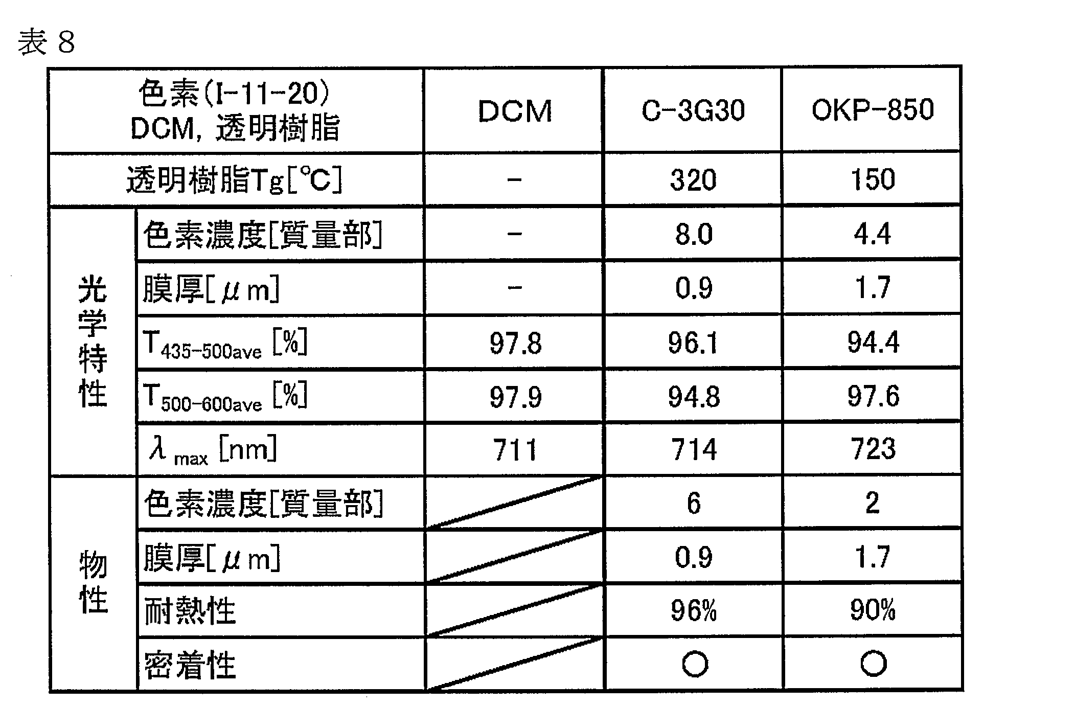
上記同様に評価した色素(I-12-15)の結果を表9に、色素(I-11-7)の結果を表10にそれぞれ示す。
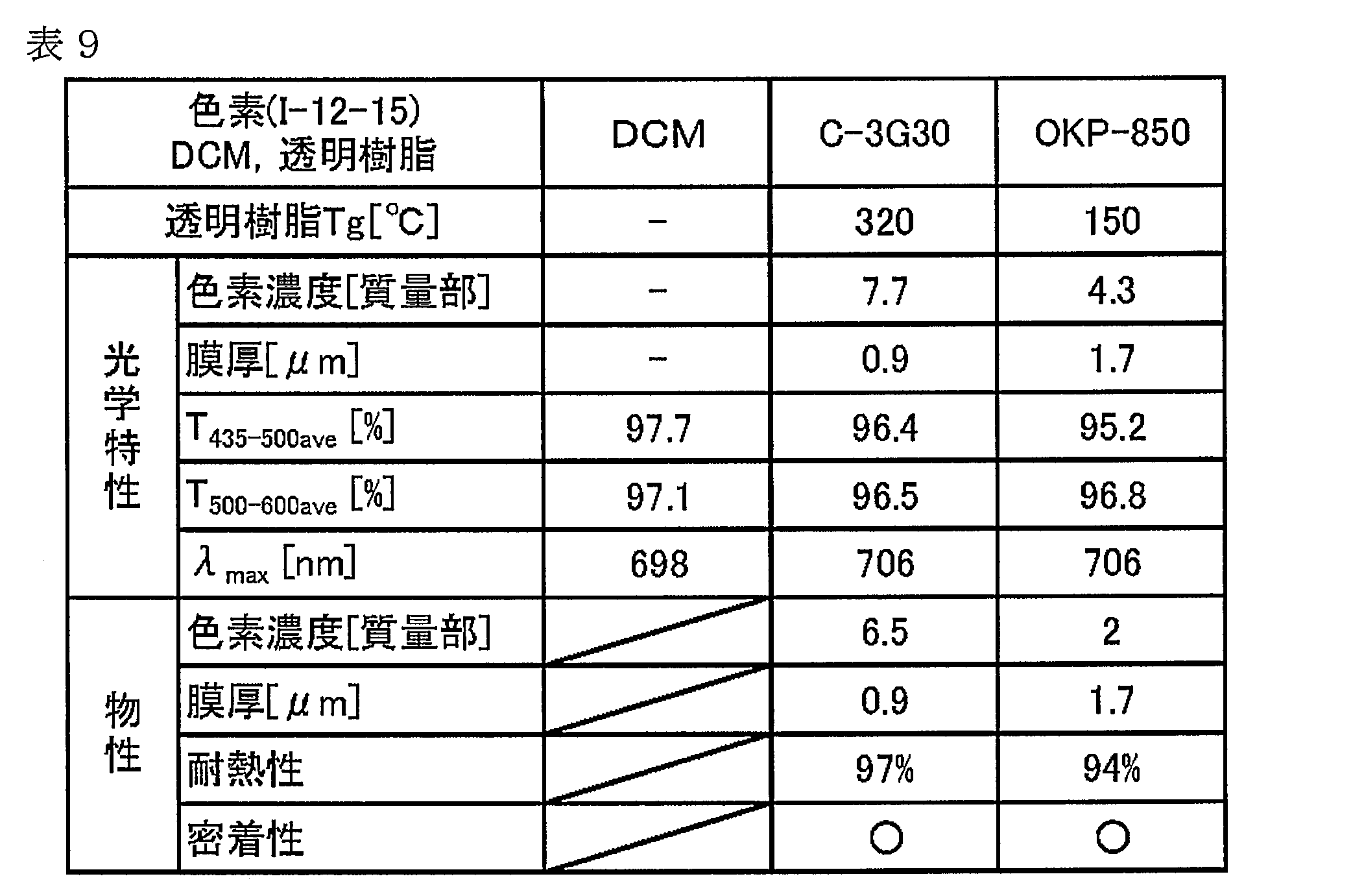
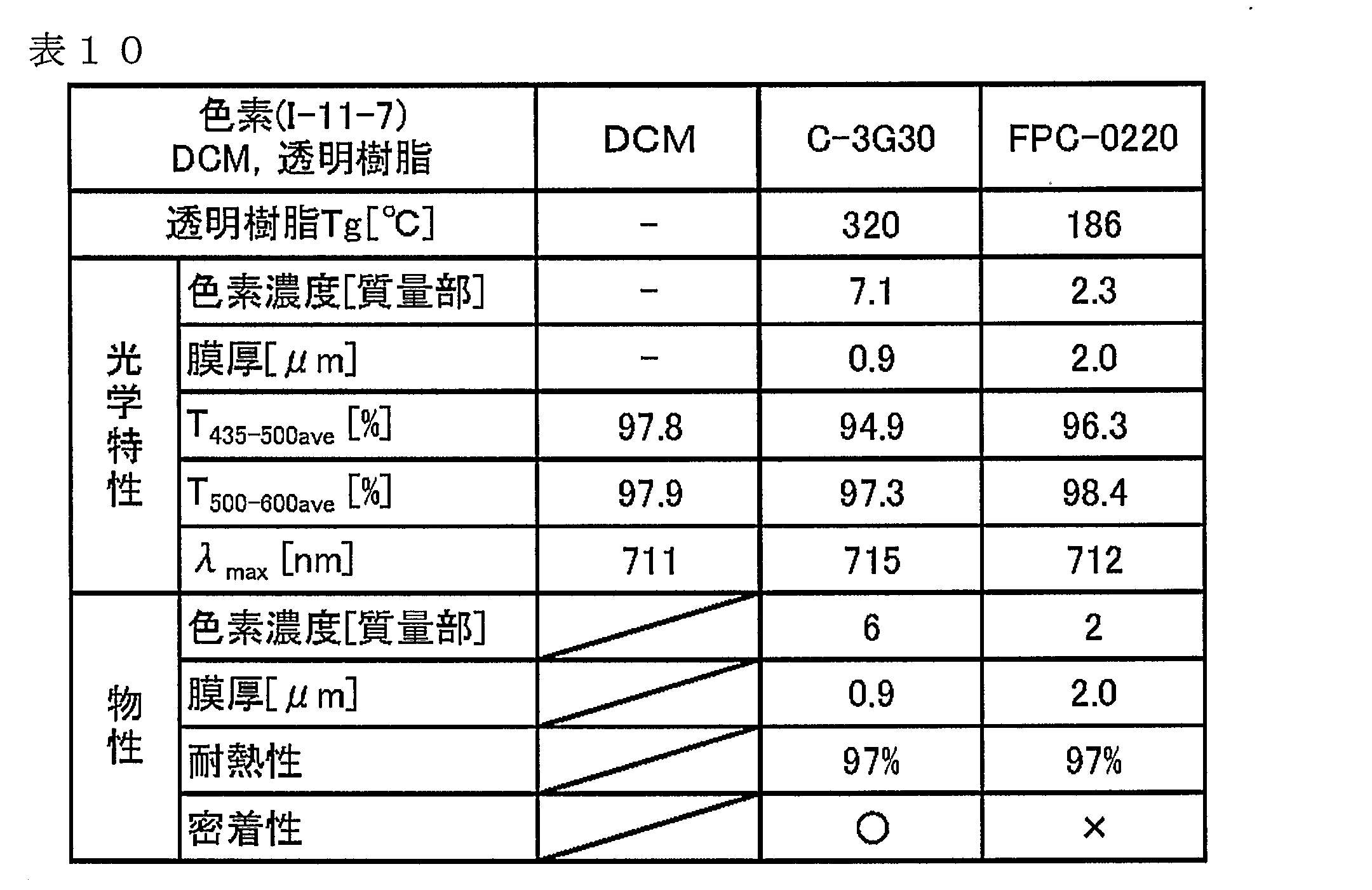
さらに、UV色素(U)である色素(M-6)について、光学特性を上記同様に評価した結果を表11に示す。また、FDN023およびFDN026については、ジクロロメタン中の分光特性とC-3G30中の分光特性をそれぞれ、表12および表13に示す。
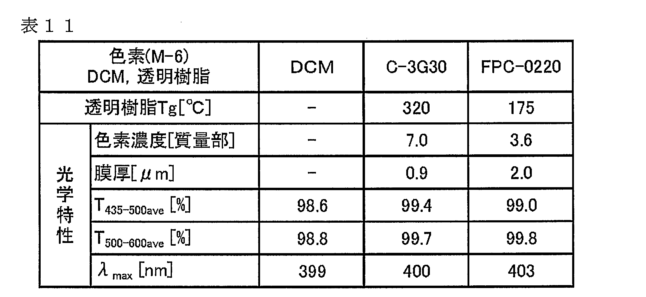


[光学フィルタの作製、評価]
(例1)
図2に示す光学フィルタ10Bと同様の構成の光学フィルタを以下のとおり製造し評価した。
(例1)
図2に示す光学フィルタ10Bと同様の構成の光学フィルタを以下のとおり製造し評価した。
樹脂基材として、ポリカーボネート樹脂フィルムである、表7に物性を示すM5-80を用いた。第2の透明樹脂として、C-3G30(樹脂ワニス)を用い、該ワニス中の透明樹脂100質量部に対して、色素(I-12-15)を9.6質量部、色素(M-6)を2.7質量部添加し、ホスト溶媒としてシクロヘキサノンを用いて塗工液を作製した。得られた塗工液をM5-80の両主面にそれぞれダイコート法で塗工し、乾燥して膜厚が0.6μmの吸収層をそれぞれ形成した。
樹脂基材上の一方の吸収層の上にNIR反射層として、蒸着によりTiO2膜とSiO2膜を交互に積層した、厚み6.7μmの誘電体多層膜からなり、入射角と各波長域における透過率の関係が表14に示される反射層を形成した。表14において、R420-650は、表14中の各入射角の光における、420~650nmの波長領域の光の最大反射率[%]を示す。λREIRSHT20は、反射層において表14中の各入射角の光に対して近赤外域側で透過率が20%を示す短波長側の波長を、λRESUVLO20は、反射層において表14中の各入射角の光に対して350~500nmの範囲で透過率が20%を示す長波長側の波長を示す。
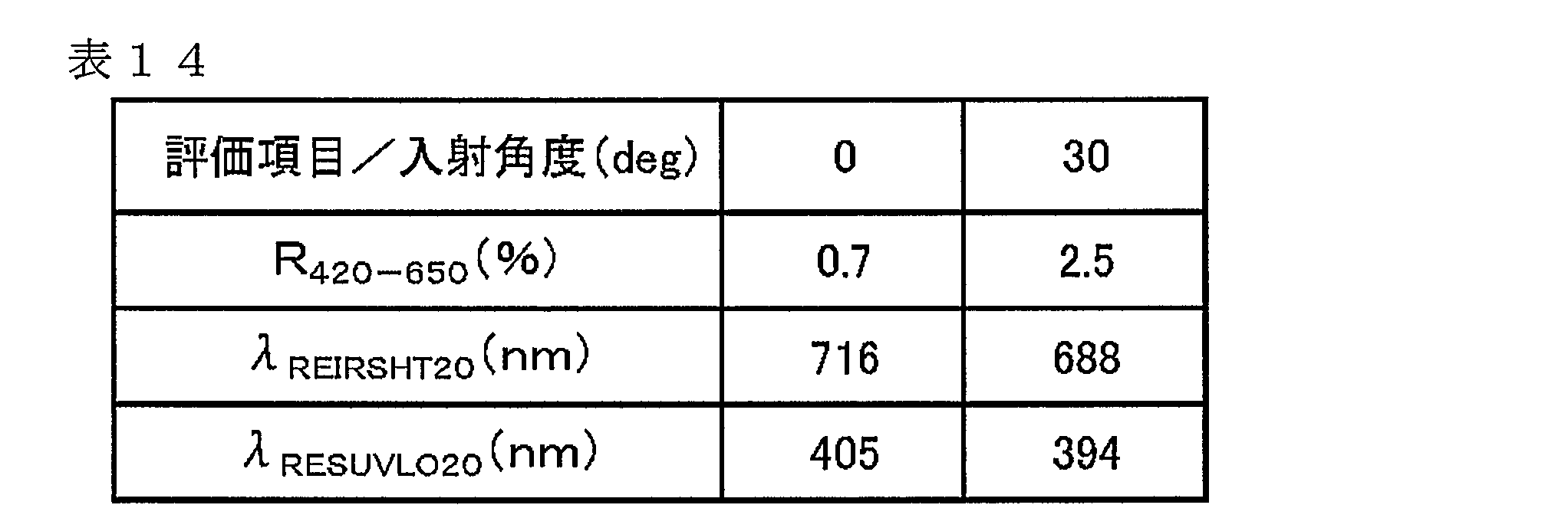
樹脂基材上の他方の吸収層の上に反射防止層として、蒸着によりTiO2膜とSiO2膜を交互に積層した、厚み3.0μmの誘電体多層膜を成膜した。
(評価)
(1)光学特性
図3に得られた光学フィルタの入射角0度および入射角30度における波長350~1100nmの分光透過率曲線を示す。得られた分光透過率曲線から、以下の光学特性を評価した。結果を表15に示す。
(1)光学特性
図3に得られた光学フィルタの入射角0度および入射角30度における波長350~1100nmの分光透過率曲線を示す。得られた分光透過率曲線から、以下の光学特性を評価した。結果を表15に示す。
(a)入射角0度と30度における435~480nmの波長領域の光の平均透過率(表中、「T435-480ave」で示す。)と、500~600nmの波長領域の光の平均透過率(表中、「T500-600ave」で示す。)。
(b)入射角0度における380~425nmの平均透過率と入射角30度における380~425nmの平均透過率の差の絶対値(表中、「ΔT380-425」で示す。)。
(c)入射角0度における615~725nmの平均透過率と入射角30度における615~725nmの平均透過率の差の絶対値(表中、「ΔT615-725」で示す。)。
(d)入射角0度における光の透過率において可視域の長波長側で透過率が20%となる波長が存在する波長(表中、「λ20」で示す。)。
(b)入射角0度における380~425nmの平均透過率と入射角30度における380~425nmの平均透過率の差の絶対値(表中、「ΔT380-425」で示す。)。
(c)入射角0度における615~725nmの平均透過率と入射角30度における615~725nmの平均透過率の差の絶対値(表中、「ΔT615-725」で示す。)。
(d)入射角0度における光の透過率において可視域の長波長側で透過率が20%となる波長が存在する波長(表中、「λ20」で示す。)。

(2)耐熱性
得られた光学フィルタを、160℃の雰囲気に30分放置する加熱試験を行った。結果は、加熱試験による割れを生じなかった。
(3)密着性
得られた光学フィルタを80℃の温水に30分浸するピール試験を実施した。結果は、ピール試験後にNIR反射層および反射防止層が光学フィルタから剥がれることはなかった。NIR反射層および反射防止層がNIR吸収層に強固に密着していることがわかる。
得られた光学フィルタを、160℃の雰囲気に30分放置する加熱試験を行った。結果は、加熱試験による割れを生じなかった。
(3)密着性
得られた光学フィルタを80℃の温水に30分浸するピール試験を実施した。結果は、ピール試験後にNIR反射層および反射防止層が光学フィルタから剥がれることはなかった。NIR反射層および反射防止層がNIR吸収層に強固に密着していることがわかる。
(例2~9)
図2に示す光学フィルタ10Bと同様の構成の光学フィルタを以下のとおり製造し評価した。樹脂基材として、表7に物性を示すM5-80(厚み80μm)、L-3G30(厚み50μm)、S5-100(厚み100μm)、L-3450(厚み50μm)、OKP-F5(厚み100μm)、またはQ65HA(厚み100μm)のフィルムを用いた。第2の透明樹脂として、C-3G30(樹脂ワニス)を用い、該ワニス中の透明樹脂100質量部に対して、色素(I-12-15)、色素(I-12-25)、色素(M-6)、色素(2)を表16および表17に示す配合量でそれぞれ添加し、ホスト溶媒としてシクロヘキサノンを用いて塗工液を作製した。得られた塗工液を各樹脂基材の両主面にそれぞれダイコート法で塗工し、乾燥して膜厚が0.55μmまたは0.9μmの吸収層をそれぞれ形成した。
図2に示す光学フィルタ10Bと同様の構成の光学フィルタを以下のとおり製造し評価した。樹脂基材として、表7に物性を示すM5-80(厚み80μm)、L-3G30(厚み50μm)、S5-100(厚み100μm)、L-3450(厚み50μm)、OKP-F5(厚み100μm)、またはQ65HA(厚み100μm)のフィルムを用いた。第2の透明樹脂として、C-3G30(樹脂ワニス)を用い、該ワニス中の透明樹脂100質量部に対して、色素(I-12-15)、色素(I-12-25)、色素(M-6)、色素(2)を表16および表17に示す配合量でそれぞれ添加し、ホスト溶媒としてシクロヘキサノンを用いて塗工液を作製した。得られた塗工液を各樹脂基材の両主面にそれぞれダイコート法で塗工し、乾燥して膜厚が0.55μmまたは0.9μmの吸収層をそれぞれ形成した。
得られた、吸収層付き樹脂基材について、波長350~1100nmの分光透過率曲線における、上記(v-1)~(v-4)に係る光学特性を評価した。なお、該光学特性は入射角0度における光学特性である。
すなわち、波長350~1100nmの分光透過率曲線における、波長435~480nmの平均内部透過率(「T435-480aveーx」と示す。)、波長500~600nmの平均内部透過率(「T500-600aveーx」と示す。)、波長600~740nmで内部透過率が20%となる波長(「λIR20」と示す。)、波長700~730nmの平均内部透過率(「T700-730aveーx」と示す。)を評価した。結果を表16に示す。なお、表16においては、以下のとおり作製される例2~例9の光学フィルタに対応して、吸収層付き樹脂基材を例2~例9で示した。

上記で得られた吸収層付き樹脂基材を用いて、例1と同様に樹脂基材上の一方の吸収層の上にNIR反射層を他方の吸収層の上に反射防止層を成膜し例2~例9の光学フィルタを作製した。得られた光学フィルタについて例1と同様の光学特性の評価を行った。結果を表17に示す。
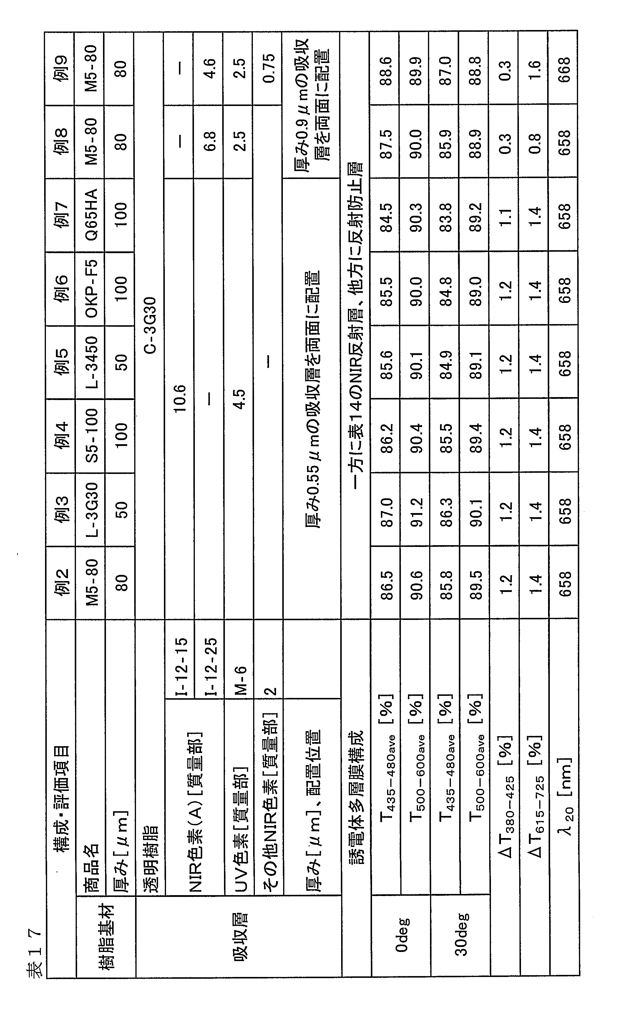
上記の試験結果から明らかなように、本発明の要件を満足する実施例の光学フィルタである例1~例4、例8、例9の光学フィルタは、可視光の高い透過性および近赤外光の高い遮蔽性を有するとともに、斜入射シフトが抑制され、さらに耐熱性、誘電体多層膜の密着性に優れる光学フィルタである。一方、比較例である例5~7の光学フィルタは、樹脂基材の可視域の吸収が大きいことに起因して、特に青色の可視光透過性を示す、T435-480aveが入射角0度および30度で低いことがわかる。
本発明を詳細にまた特定の実施態様を参照して説明したが、本発明の精神と範囲を逸脱することなく様々な変更や修正を加えることができることは当業者にとって明らかである。本出願は2018年9月12日出願の日本特許出願(特願2018-170906)に基づくものであり、その内容はここに参照として取り込まれる。
本発明の光学フィルタは、樹脂材料を基材として用いた近赤外カットフィルタにおいて、可視光の高い透過性および近赤外光の高い遮蔽性を有するとともに、該光学特性の耐熱性に優れるので、近年、高性能化、小型化が進むデジタルスチルカメラ等の撮像装置等の用途に有用である。
10A,10B…光学フィルタ、1…樹脂基材、2,2a,2b…吸収層、3a,3b…誘電体多層膜。
Claims (12)
- 厚みが20μm以上110μm以下の樹脂基材と、
前記樹脂基材の少なくとも一方の主面上に配置される厚みが0.25μm以上12μm以下の吸収層と、
前記樹脂基材の両方の主面の上方に最外層として配置される誘電体多層膜と、を有する光学フィルタであって、
前記誘電体多層膜の少なくとも一方は近赤外線反射層であり、
前記樹脂基材は、ガラス転移温度が170℃以上である第1の透明樹脂を主成分とし、前記第1の透明樹脂は、厚み100μmのときの波長350~1100nmの分光透過率曲線において、波長350~450nmの平均内部透過率が95%以上であり、波長400~450nmの最小内部透過率が97%以上であり、波長500nm以下の領域で内部透過率が90%となる波長が350nm以下であり、
前記吸収層は、近赤外線吸収色素(A)と、ガラス転移温度が170℃以上である第2の透明樹脂を含み、前記近赤外線吸収色素(A)は、前記第2の透明樹脂との関係が下記(ii-1)および(ii-2)を満足する、光学フィルタ。
(ii-1)前記近赤外線吸収色素(A)を前記第2の透明樹脂に含有させて測定される、波長400~800nmの分光透過率曲線において、最大吸収波長λmax(A)TRが680~745nmの波長領域にある。
(ii-2)前記近赤外線吸収色素(A)を前記第2の透明樹脂に含有させて、前記最大吸収波長λmax(A)TRにおける内部透過率を1%に合わせたときの、波長350~1100nmの分光透過率曲線において、435~500nmの波長領域の光の平均内部透過率T435-500ave(A)TRおよび500~600nmの波長領域の光の平均内部透過率T500-600ave(A)TRがともに94%以上である。 - 前記第1の透明樹脂は、ポリイミド樹脂およびガラス転移温度が200℃以上であるポリカーボネート樹脂から選ばれる少なくとも1種を含み、前記第1の透明樹脂は、厚み100μmのときの波長350~1100nmの分光透過率曲線において、波長350~450nmの平均内部透過率が98%以上であり、波長400~450nmの最小内部透過率が98%以上であり、波長500nm以下の領域で内部透過率が90%となる波長が340nm以下である、請求項1記載の光学フィルタ。
- 前記第2の透明樹脂は、ポリイミド樹脂を含む請求項1または2に記載の光学フィルタ。
- 前記吸収層は、厚みが5μm以下であり、前記第2の透明樹脂の100質量部に対して前記近赤外線吸収色素を5~20質量部含有する、請求項1~3のいずれか1項に記載の光学フィルタ。
- 前記近赤外線吸収色素(A)は、スクアリリウム色素を含む請求項1~4のいずれか1項に記載の光学フィルタ。
- 前記スクアリリウム色素は、下式(I)または(II)で示される化合物である、請求項5記載の光学フィルタ。
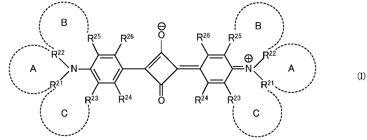
ただし、式(I)中の記号は以下のとおりである。
R24およびR26は、それぞれ独立して、水素原子、ハロゲン原子、水酸基、炭素数1~20のアルキル基もしくはアルコキシ基、炭素数1~10のアシルオキシ基、炭素数6~11のアリール基、置換基を有していてもよく炭素原子間に酸素原子を有していてもよい炭素数7~18のアルアリール基、-NR27R28(R27およびR28は、それぞれ独立して、水素原子、炭素数1~20のアルキル基、-C(=O)-R29(R29は、水素原子、ハロゲン原子、水酸基、置換基を有していてもよく、炭素原子間に不飽和結合、酸素原子、飽和もしくは不飽和の環構造を含んでよい炭素数1~25の炭化水素基)、-NHR30、または、-SO2-R30(R30は、それぞれ1つ以上の水素原子がハロゲン原子、水酸基、カルボキシ基、スルホ基、またはシアノ基で置換されていてもよく、炭素原子間に不飽和結合、酸素原子、飽和もしくは不飽和の環構造を含んでよい炭素数1~25の炭化水素基)を示す。)、または、下記式(S)で示される基(R41、R42は、独立して、水素原子、ハロゲン原子、または炭素数1~10のアルキル基もしくはアルコキシ基を示す。kは2または3である。)を示す。
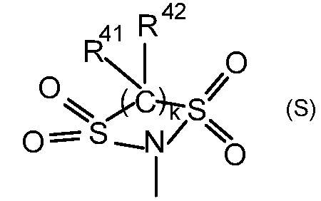
R21とR22、R22とR25、およびR21とR23は、互いに連結して窒素原子と共に員数が5または6のそれぞれ複素環A、複素環B、および複素環Cを形成してもよい。
複素環Aが形成される場合のR21とR22は、これらが結合した2価の基-Q-として、水素原子が炭素数1~6のアルキル基、炭素数6~10のアリール基または置換基を有していてもよい炭素数1~10のアシルオキシ基で置換されてもよいアルキレン基、またはアルキレンオキシ基を示す。
複素環Bが形成される場合のR22とR25、および複素環Cが形成される場合のR21とR23は、これらが結合したそれぞれ2価の基-X1-Y1-および-X2-Y2-(窒素に結合する側がX1およびX2)として、X1およびX2がそれぞれ下記式(1x)または(2x)で示される基であり、Y1およびY2がそれぞれ下記式(1y)~(5y)から選ばれるいずれかで示される基である。X1およびX2が、それぞれ下記式(2x)で示される基の場合、Y1およびY2はそれぞれ単結合であってもよく、その場合、炭素原子間に酸素原子を有してもよい。
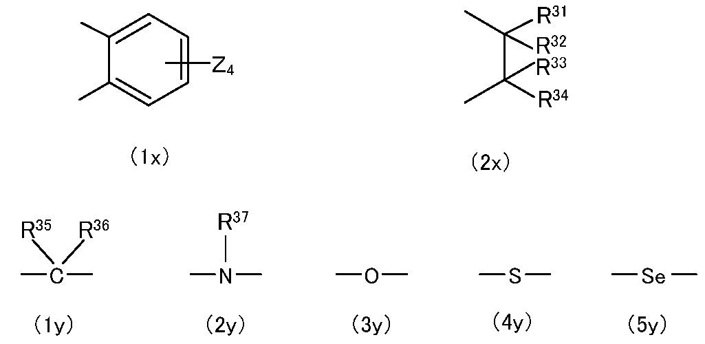
式(1x)中、4個のZは、それぞれ独立して水素原子、水酸基、炭素数1~6のアルキル基もしくはアルコキシ基、または-NR38R39(R38およびR39は、それぞれ独立して、水素原子または炭素数1~20のアルキル基を示す)を示す。R31~R36はそれぞれ独立して水素原子、炭素数1~6のアルキル基または炭素数6~10のアリール基を、R37は炭素数1~6のアルキル基または炭素数6~10のアリール基を示す。
R27、R28、R29、R31~R37、複素環を形成していない場合のR21~R23、およびR25は、これらのうちの他のいずれかと互いに結合して5員環または6員環を形成してもよい。R31とR36、R31とR37は直接結合してもよい。
複素環を形成していない場合の、R21、R22、R23およびR25は、それぞれ独立して、水素原子、ハロゲン原子、水酸基、炭素数1~20のアルキル基もしくはアルコキシ基、炭素数1~10のアシルオキシ基、炭素数6~11のアリール基、または、置換基を有していてもよく炭素原子間に酸素原子を有していてもよい炭素数7~18のアルアリール基を示す。
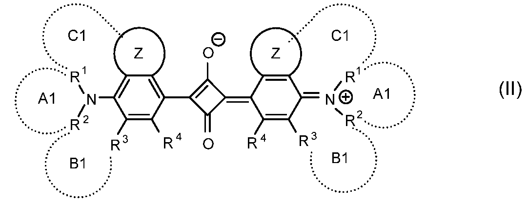
ただし、式(II)中の記号は以下のとおりである。
環Zは、それぞれ独立して、ヘテロ原子を環中に0~3個有する5員環または6員環であり、環Zが有する水素原子は置換されていてもよい。
R1とR2、R2とR3、およびR1と環Zを構成する炭素原子またはヘテロ原子は、互いに連結して窒素原子とともにそれぞれヘテロ環A1、ヘテロ環B1およびヘテロ環C1を形成していてもよく、その場合、ヘテロ環A1、ヘテロ環B1およびヘテロ環C1が有する水素原子は置換されていてもよい。ヘテロ環を形成していない場合のR1およびR2は、それぞれ独立して、水素原子、ハロゲン原子、または、炭素原子間に不飽和結合、ヘテロ原子、飽和もしくは不飽和の環構造を含んでよく、置換基を有してもよい炭化水素基を示す。R4およびヘテロ環を形成していない場合のR3は、それぞれ独立して、水素原子、ハロゲン原子、または炭素原子間にヘテロ原子を含んでもよく、置換基を有してもよいアルキル基もしくはアルコキシ基を示す。 - 前記第2の透明樹脂はポリイミド樹脂であり、前記吸収層を前記樹脂基材の両方の主面上に備え、前記吸収層の厚みはいずれも1.5μm以下である請求項1~6のいずれか1項に記載の光学フィルタ。
- 前記吸収層が前記樹脂基材の少なくとも一方の主面上に配置された吸収層付き樹脂基材は、波長350~1100nmの分光透過率曲線において、波長435~480nmの平均内部透過率が90.5%以上であり、波長500~600nmの平均内部透過率が90.5%以上であり、波長600~740nmで内部透過率が20%となる波長が650~685nmの波長領域にあり、波長700~730nmの平均内部透過率が3%以下である請求項1~7のいずれか1項に記載の光学フィルタ。
- 前記吸収層は、さらに、ジクロロメタンに溶解して測定される波長350~1100nmの分光透過率曲線において、最大吸収波長λmax(U)DCMが380~420nmの波長領域にある紫外線吸収色素(U)を含む請求項1~8のいずれか1項に記載の光学フィルタ。
- 前記紫外線吸収色素(U)は、メロシアニン色素を含む請求項9記載の光学フィルタ。
- 下記(I-1)~(I-5)の要件を満足する請求項1~10のいずれか1項に記載の光学フィルタ。
(I-1)入射角0度における435~480nmの波長領域の光の平均透過率が86%以上であり、500~600nmの波長領域の光の平均透過率が89%以上である。
(I-2)入射角30度における435~480nmの波長領域の光の平均透過率が85%以上であり、500~600nmの波長領域の光の平均透過率が89%以上である。
(I-3)入射角0度における380~425nmの平均透過率と入射角30度における380~425nmの平均透過率の差の絶対値が3%以下である。
(I-4)入射角0度における615~725nmの平均透過率と入射角30度における615~725nmの平均透過率の差の絶対値が3%以下である。
(I-5)入射角0度における光の透過率において、波長領域650~685nmに透過率が20%となる波長が存在する。 - 請求項1~11のいずれか1項に記載の光学フィルタを備える撮像装置。
Priority Applications (4)
| Application Number | Priority Date | Filing Date | Title |
|---|---|---|---|
| JP2020504737A JP7298072B2 (ja) | 2018-09-12 | 2019-09-11 | 光学フィルタおよび撮像装置 |
| CN201980059518.3A CN112689780A (zh) | 2018-09-12 | 2019-09-11 | 光学滤波器和摄像装置 |
| US17/193,151 US12181696B2 (en) | 2018-09-12 | 2021-03-05 | Optical filter and imaging device |
| JP2023094313A JP2023111981A (ja) | 2018-09-12 | 2023-06-07 | 光学フィルタおよび撮像装置 |
Applications Claiming Priority (2)
| Application Number | Priority Date | Filing Date | Title |
|---|---|---|---|
| JP2018-170906 | 2018-09-12 | ||
| JP2018170906 | 2018-09-12 |
Related Child Applications (1)
| Application Number | Title | Priority Date | Filing Date |
|---|---|---|---|
| US17/193,151 Continuation US12181696B2 (en) | 2018-09-12 | 2021-03-05 | Optical filter and imaging device |
Publications (1)
| Publication Number | Publication Date |
|---|---|
| WO2020054786A1 true WO2020054786A1 (ja) | 2020-03-19 |
Family
ID=69777864
Family Applications (1)
| Application Number | Title | Priority Date | Filing Date |
|---|---|---|---|
| PCT/JP2019/035779 Ceased WO2020054786A1 (ja) | 2018-09-12 | 2019-09-11 | 光学フィルタおよび撮像装置 |
Country Status (4)
| Country | Link |
|---|---|
| US (1) | US12181696B2 (ja) |
| JP (2) | JP7298072B2 (ja) |
| CN (1) | CN112689780A (ja) |
| WO (1) | WO2020054786A1 (ja) |
Cited By (4)
| Publication number | Priority date | Publication date | Assignee | Title |
|---|---|---|---|---|
| JP2022001928A (ja) * | 2020-06-22 | 2022-01-06 | Agc株式会社 | 光学フィルタ |
| JPWO2022065170A1 (ja) * | 2020-09-23 | 2022-03-31 | ||
| JP2023004105A (ja) * | 2021-06-25 | 2023-01-17 | Jsr株式会社 | 基材、光学フィルターおよび光学センサー装置 |
| CN116057428A (zh) * | 2020-07-27 | 2023-05-02 | Agc株式会社 | 滤光片 |
Families Citing this family (1)
| Publication number | Priority date | Publication date | Assignee | Title |
|---|---|---|---|---|
| JPWO2020203991A1 (ja) * | 2019-03-29 | 2020-10-08 |
Citations (5)
| Publication number | Priority date | Publication date | Assignee | Title |
|---|---|---|---|---|
| JP2002372603A (ja) * | 2001-06-15 | 2002-12-26 | Nikon Corp | 光通信用光学部品及びその製造方法 |
| WO2015056734A1 (ja) * | 2013-10-17 | 2015-04-23 | Jsr株式会社 | 光学フィルター、固体撮像装置およびカメラモジュール |
| WO2017094858A1 (ja) * | 2015-12-01 | 2017-06-08 | 旭硝子株式会社 | 光学フィルタおよび撮像装置 |
| WO2017135359A1 (ja) * | 2016-02-02 | 2017-08-10 | 旭硝子株式会社 | 近赤外線吸収色素、光学フィルタおよび撮像装置 |
| JP2018084647A (ja) * | 2016-11-22 | 2018-05-31 | 京セラ株式会社 | 赤外線カットフィルタおよび光学素子用パッケージ |
Family Cites Families (22)
| Publication number | Priority date | Publication date | Assignee | Title |
|---|---|---|---|---|
| DE2753230A1 (de) * | 1977-11-29 | 1979-06-07 | Bayer Ag | Verfahren zur herstellung aromatischer polyester |
| US5543086A (en) | 1987-08-12 | 1996-08-06 | Gentex Corporation | Squarylium dyestuffs and compostions containing same |
| JP3995387B2 (ja) | 2000-04-13 | 2007-10-24 | 帝人株式会社 | 偏光板保護用透明フィルム及びそれを用いてなる偏光板 |
| KR20070116228A (ko) * | 2005-03-29 | 2007-12-07 | 닛산 가가쿠 고교 가부시키 가이샤 | 폴리아믹산, 폴리이미드 및 그 제조 방법 |
| JP5489669B2 (ja) | 2008-11-28 | 2014-05-14 | Jsr株式会社 | 近赤外線カットフィルターおよび近赤外線カットフィルターを用いた装置 |
| JP5383755B2 (ja) | 2010-12-17 | 2014-01-08 | 株式会社日本触媒 | 光選択透過フィルター、樹脂シート及び固体撮像素子 |
| JP2013029708A (ja) | 2011-07-29 | 2013-02-07 | Fujifilm Corp | 近赤外線カットフィルターおよび近赤外線カットフィルターの製造方法 |
| JP2013067718A (ja) * | 2011-09-22 | 2013-04-18 | Mitsubishi Gas Chemical Co Inc | 光学積層フィルム |
| WO2013054864A1 (ja) | 2011-10-14 | 2013-04-18 | Jsr株式会社 | 光学フィルターならびに該光学フィルターを用いた固体撮像装置およびカメラモジュール |
| WO2013146460A1 (ja) | 2012-03-30 | 2013-10-03 | 新日本理化株式会社 | 高透明性ポリイミド樹脂 |
| KR101983742B1 (ko) * | 2012-06-25 | 2019-05-29 | 제이에스알 가부시끼가이샤 | 고체 촬상 소자용 광학 필터, 고체 촬상 장치 및 카메라 모듈 |
| US9090776B2 (en) | 2012-09-04 | 2015-07-28 | Exciton, Inc. | Squarylium dyes |
| WO2014088063A1 (ja) | 2012-12-06 | 2014-06-12 | 旭硝子株式会社 | 近赤外線カットフィルタ |
| JP6269657B2 (ja) * | 2013-04-10 | 2018-01-31 | 旭硝子株式会社 | 赤外線遮蔽フィルタ、固体撮像素子、および撮像・表示装置 |
| JP6380390B2 (ja) | 2013-05-29 | 2018-08-29 | Jsr株式会社 | 光学フィルターおよび前記フィルターを用いた装置 |
| JP5650810B2 (ja) | 2013-06-24 | 2015-01-07 | 株式会社ニデック | 眼軸長測定装置 |
| JP6103152B2 (ja) * | 2015-01-14 | 2017-03-29 | 旭硝子株式会社 | 近赤外線カットフィルタおよび固体撮像装置 |
| WO2016114363A1 (ja) * | 2015-01-14 | 2016-07-21 | 旭硝子株式会社 | 近赤外線カットフィルタおよび撮像装置 |
| CN109320992B (zh) * | 2015-02-18 | 2020-05-05 | Agc株式会社 | 方酸鎓系色素、树脂膜、光学滤波器和摄像装置 |
| WO2016181987A1 (ja) | 2015-05-12 | 2016-11-17 | 旭硝子株式会社 | 光学フィルタおよび撮像装置 |
| JP6605039B2 (ja) | 2015-12-17 | 2019-11-13 | 富士フイルム株式会社 | 近赤外線吸収性組成物、膜、赤外線カットフィルタ、固体撮像素子、赤外線吸収剤および化合物 |
| JP7036021B2 (ja) * | 2016-10-12 | 2022-03-15 | コニカミノルタ株式会社 | 透明ポリイミド樹脂、透明ポリイミド樹脂組成物、透明ポリイミド樹脂フィルム、赤外線吸収組成物、赤外線カットフィルター及び透明ポリイミド樹脂フィルムの製造方法 |
-
2019
- 2019-09-11 CN CN201980059518.3A patent/CN112689780A/zh active Pending
- 2019-09-11 JP JP2020504737A patent/JP7298072B2/ja active Active
- 2019-09-11 WO PCT/JP2019/035779 patent/WO2020054786A1/ja not_active Ceased
-
2021
- 2021-03-05 US US17/193,151 patent/US12181696B2/en active Active
-
2023
- 2023-06-07 JP JP2023094313A patent/JP2023111981A/ja active Pending
Patent Citations (5)
| Publication number | Priority date | Publication date | Assignee | Title |
|---|---|---|---|---|
| JP2002372603A (ja) * | 2001-06-15 | 2002-12-26 | Nikon Corp | 光通信用光学部品及びその製造方法 |
| WO2015056734A1 (ja) * | 2013-10-17 | 2015-04-23 | Jsr株式会社 | 光学フィルター、固体撮像装置およびカメラモジュール |
| WO2017094858A1 (ja) * | 2015-12-01 | 2017-06-08 | 旭硝子株式会社 | 光学フィルタおよび撮像装置 |
| WO2017135359A1 (ja) * | 2016-02-02 | 2017-08-10 | 旭硝子株式会社 | 近赤外線吸収色素、光学フィルタおよび撮像装置 |
| JP2018084647A (ja) * | 2016-11-22 | 2018-05-31 | 京セラ株式会社 | 赤外線カットフィルタおよび光学素子用パッケージ |
Cited By (10)
| Publication number | Priority date | Publication date | Assignee | Title |
|---|---|---|---|---|
| JP2022001928A (ja) * | 2020-06-22 | 2022-01-06 | Agc株式会社 | 光学フィルタ |
| JP7415815B2 (ja) | 2020-06-22 | 2024-01-17 | Agc株式会社 | 光学フィルタ |
| CN116057428A (zh) * | 2020-07-27 | 2023-05-02 | Agc株式会社 | 滤光片 |
| JP2024177587A (ja) * | 2020-07-27 | 2024-12-19 | Agc株式会社 | 光学フィルタ |
| JP7823708B2 (ja) | 2020-07-27 | 2026-03-04 | Agc株式会社 | 光学フィルタ |
| JPWO2022065170A1 (ja) * | 2020-09-23 | 2022-03-31 | ||
| WO2022065170A1 (ja) * | 2020-09-23 | 2022-03-31 | Agc株式会社 | 光学フィルタ |
| JP7775831B2 (ja) | 2020-09-23 | 2025-11-26 | Agc株式会社 | 光学フィルタ |
| JP2023004105A (ja) * | 2021-06-25 | 2023-01-17 | Jsr株式会社 | 基材、光学フィルターおよび光学センサー装置 |
| JP7630760B2 (ja) | 2021-06-25 | 2025-02-18 | Jsr株式会社 | 基材、光学フィルターおよび光学センサー装置 |
Also Published As
| Publication number | Publication date |
|---|---|
| CN112689780A (zh) | 2021-04-20 |
| JPWO2020054786A1 (ja) | 2021-08-30 |
| US12181696B2 (en) | 2024-12-31 |
| US20210191012A1 (en) | 2021-06-24 |
| JP2023111981A (ja) | 2023-08-10 |
| JP7298072B2 (ja) | 2023-06-27 |
Similar Documents
| Publication | Publication Date | Title |
|---|---|---|
| JP7298072B2 (ja) | 光学フィルタおよび撮像装置 | |
| JP6881660B2 (ja) | 光学フィルターおよび光学センサー装置 | |
| JP7342944B2 (ja) | 光学フィルタおよび撮像装置 | |
| JP6627864B2 (ja) | 光学フィルターおよび光学フィルターを用いた装置 | |
| JP7456525B2 (ja) | 光学フィルタおよび撮像装置 | |
| JP2021039369A (ja) | 光学フィルターおよび光学フィルターを用いた装置 | |
| JP7823708B2 (ja) | 光学フィルタ | |
| JP2022189736A (ja) | 組成物、光学部材および光学部材を備えた装置 | |
| WO2023002923A1 (ja) | 光学フィルタ | |
| JP7415815B2 (ja) | 光学フィルタ | |
| JP2026015465A (ja) | 光学フィルタ | |
| TW202242010A (zh) | 基材、光學濾波器、固體攝像裝置及照相機模組 | |
| JP2022165848A (ja) | 光学フィルターおよび光学センサー装置 |
Legal Events
| Date | Code | Title | Description |
|---|---|---|---|
| ENP | Entry into the national phase |
Ref document number: 2020504737 Country of ref document: JP Kind code of ref document: A |
|
| 121 | Ep: the epo has been informed by wipo that ep was designated in this application |
Ref document number: 19860368 Country of ref document: EP Kind code of ref document: A1 |
|
| NENP | Non-entry into the national phase |
Ref country code: DE |
|
| 122 | Ep: pct application non-entry in european phase |
Ref document number: 19860368 Country of ref document: EP Kind code of ref document: A1 |